

Page 1
MICROFILM
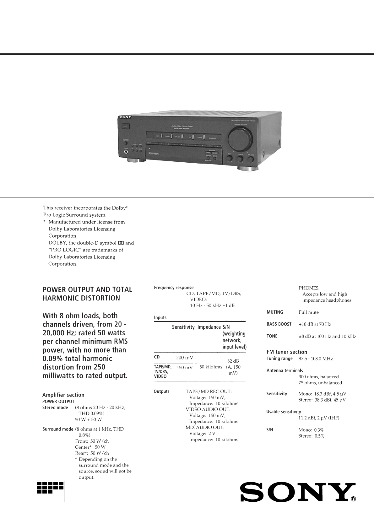
STR-V200
SERVICE MANUAL
US Model
SPECIFICATIONS
FM STEREO/FM-AM RECEIVER
— Continued on next page —
– 1 –
Page 2
SAFETY CHECK-OUT
0.15µF
To Exposed Metal
Parts on Set
1.5k
Ω
AC
voltmeter
(0.75V)
Earth Ground
After correcting the original service problem, perform the following safety checks before releasing the set to the customer:
Check the antenna terminals, metal trim, “metallized” knobs, screws,
and all other exposed metal parts for A C leakage. Check leakage as
described below.
LEAKAGE
The AC leakage from any exposed metal part to earth Ground and
from all exposed metal parts to any exposed metal part having a
return to chassis, must not exceed 0.5 mA (500 microampers). Leakage current can be measured by any one of three methods.
1. A commercial leakage tester, such as the Simpson 229 or RCA
WT-540A. Follow the manufacturers’ instructions to use these
instruments.
2. A battery-operated AC milliammeter. The Data Precision 245
digital multimeter is suitable for this job.
3. Measuring the voltage drop across a resistor by means of a V OM
or battery-operated AC voltmeter. The “limit” indication is 0.75
V, so analog meters must have an accurate low-voltage scale.
The Simpson 250 and Sanwa SH-63Trd are examples of a passive VOM that is suitable. Nearly all battery operated digital
multimeters that have a 2V AC range are suitable. (See Fig. A)
Fig. A. Using an AC voltmeter to check AC leakage.
Notes on chip component replacement
• Never reuse a disconnected chip component.
• Notice that the minus side of a tantalum capacitor may be
damaged by heat.
SAFETY-RELATED COMPONENT WARNING !!
COMPONENTS IDENTIFIED BY MARK ! OR DO TTED LINE
WITH MARK ! ON THE SCHEMATIC DIAGRAMS AND IN
THE PARTS LIST ARE CRITICAL TO SAFE OPERATION.
REPLACE THESE COMPONENTS WITH SONY PARTS
WHOSE PART NUMBERS APPEAR AS SHOWN IN THIS
MANUAL OR IN SUPPLEMENTS PUBLISHED BY SONY.
– 2 –
Page 3

TABLE OF CONTENTS
1. SERVICING NOTE ..........................................................3
2. GENERAL .......................................................................... 4
3. DIAGRAMS
3-1. Circuit Boards Location ........................................................ 6
3-2. Schematic Diagram – Main (1/3) Section –..........................7
3-3. Schematic Diagram – Main (2/3) Section –..........................9
3-4. Schematic Diagram – Main (3/3) Section –........................11
3-5. Schematic Diagram – Display Section – ............................ 13
3-6. Schematic Diagram – Panel Section – ................................15
3-7. Printed Wiring Board – Main Section – ..............................17
3-8. Printed Wiring Board – Power Section – ............................21
3-9. Printed Wiring Board – Display Section – ..........................25
3-10. Printed Wiring Board – 10 Key Section – ........................ 29
3-11. Printed Wiring Board – Panel Section –...........................31
3-12. IC Pin Functions ............................................................... 33
3-13. IC Block Diagrams ........................................................... 35
SECTION 1
SERVICING NOTE
4. EXPLODED VIEWS
4-1. Case Section........................................................................ 37
4-2. Chassis Section ................................................................... 38
5. ELECTRICAL PARTS LIST ........................................ 39
FACTORY SET
Mode which sets the preset settings of the unit to that at shipment.
Procedure:
While pressing the VIDEO button and TV/DBS button together, press the 1/u button to turn on the power.
“FACTORY” will be displayed and factory settings executed.
INITIALIZATION
Mode which erases all the preset settings of the unit.
Use this mode when returning the unit to the customer.
Procedure:
While pressing the VIDEO button, TV/DBS button, and TAPE/MD button together, press the 1/u button to turn on the power.
“INITIAL” will be displayed and initialization executed.
FLUORESCENT INDICATOR TUBE LIGHTING CHECK
Mode which lights up the whole fluorescent indicator tube or partially.
Procedure:
While pressing the TV/DBS button and TAPE/MD button together, press the 1/u button to turn on the power.
The fluorescent indicator tube will light up in about 0.5 seconds, and then start to light up partially. After partial lighting completes, the
BASS BOOST indicator will light up, “FINISH” will be displayed, indicating that fluorescent indicator tube lighting check has completed.
SWITCHING OF 9 kHz/10 kHz AM CHANNEL STEP
The AM channels of this unit can be switched between 9 kHz and 10 kHz.
Procedure:
Set FUNCTION to AM and turn off the power.
While pressing the TUNING + button, press the 1/u button to turn on the power.
“9 k STEP” or “10 k STEP” will be displayed, and the channel step will be switched.
– 3 –
Page 4
Front Panel Descriptions
SECTION 2
GENERAL
1
26
25
23
24
1 1/u button
2 VIDEO button
3 TV/DBS button
4 TAPE/MD button
5 CD button
6 TUNER button
7 BASS BOOST indicator
8 MASTER VOLUME knob
9 BALANCE knob
10 TREBLE knob
11 BASS knob
12 SURROUND ON/OFF button
13 SET UP button
14 EFFECT/DELAY TIME button
15 SURROUND MODE button
16 Numeral (1 to 0) button
17 Display window
18 DIRECT button
19 SHIFT button
20 MEMORY button
21 AM button
22 TUNING + button
23 FM button
24 TUNING – button
25 PHONES jack
26 SPEAKERS Ø ON/ø OFF button
20
3
465
17
16
782
12
1011131415
918192122
– 4 –
Page 5
This section is extracted from
instruction manual.
– 5 –
Page 6
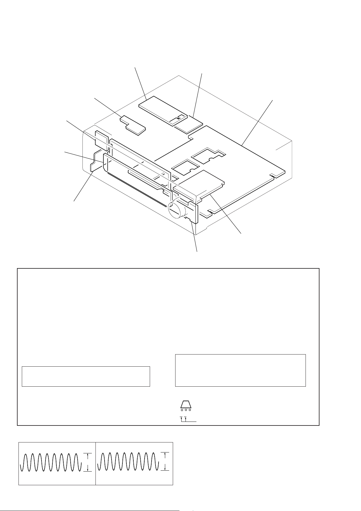
3-1. CIRCUIT BOARDS LOCATION
SECTION 3
DIAGRAMS
SECONDARY board
STANDBY board
PRIMARY board
POWER SW board
KEY board
SPEAKER SW board
MAIN board
VOL-TONE board
DISPLAY board
THIS NOTE IS COMMON FOR PRINTED WIRING
BOARDS AND SCHEMATIC DIAGRAMS.
(In addition to this, the necessary note is printed
in each block.)
For schematic diagrams.
Note:
•All capacitors are in µF unless otherwise noted. pF: µµF
50 WV or less are not indicated except for electrolytics
and tantalums.
•All resistors are in Ω and
specified.
¢
•
•2: nonflammable resistor.
•C: panel designation.
Note:The components identified by mark ! or dotted line
•U: B+ Line.
•V: B– Line.
•Voltages and waveforms are dc with respect to ground
: internal component.
with mark ! are critical for safety.
Replace only with part number specified.
under no-signal (detuned) conditions.
no mark: FM
1
/4 W or less unless otherwise
WAVEFORMS
1
2
•Voltages are taken with a VOM (Input impedance 10 MΩ).
Voltage variations may be noted due to normal production tolerances.
•Waveforms are taken with a oscilloscope.
Voltage variations may be noted due to normal production tolerances.
•Circled numbers refer to waveforms.
•Signal path.
F : FM
For printed wiring boards.
Note:
•X: parts extracted from the component side.
•b: Pattern of the conductor side.
Caution:
Pattern face side: Parts on the pattern face side seen from
(Conductor Side) the pattern face are indicated.
Parts face side: Parts on the parts face side seen from
(Component Side)the parts face are indicated.
•Indication of transistor
C
EB
These are omitted
8MHz
IC300 @¢
4.8Vp-p
5.4Vp-p
4.19MHz
IC201 #¢ X1
– 6 –
Page 7
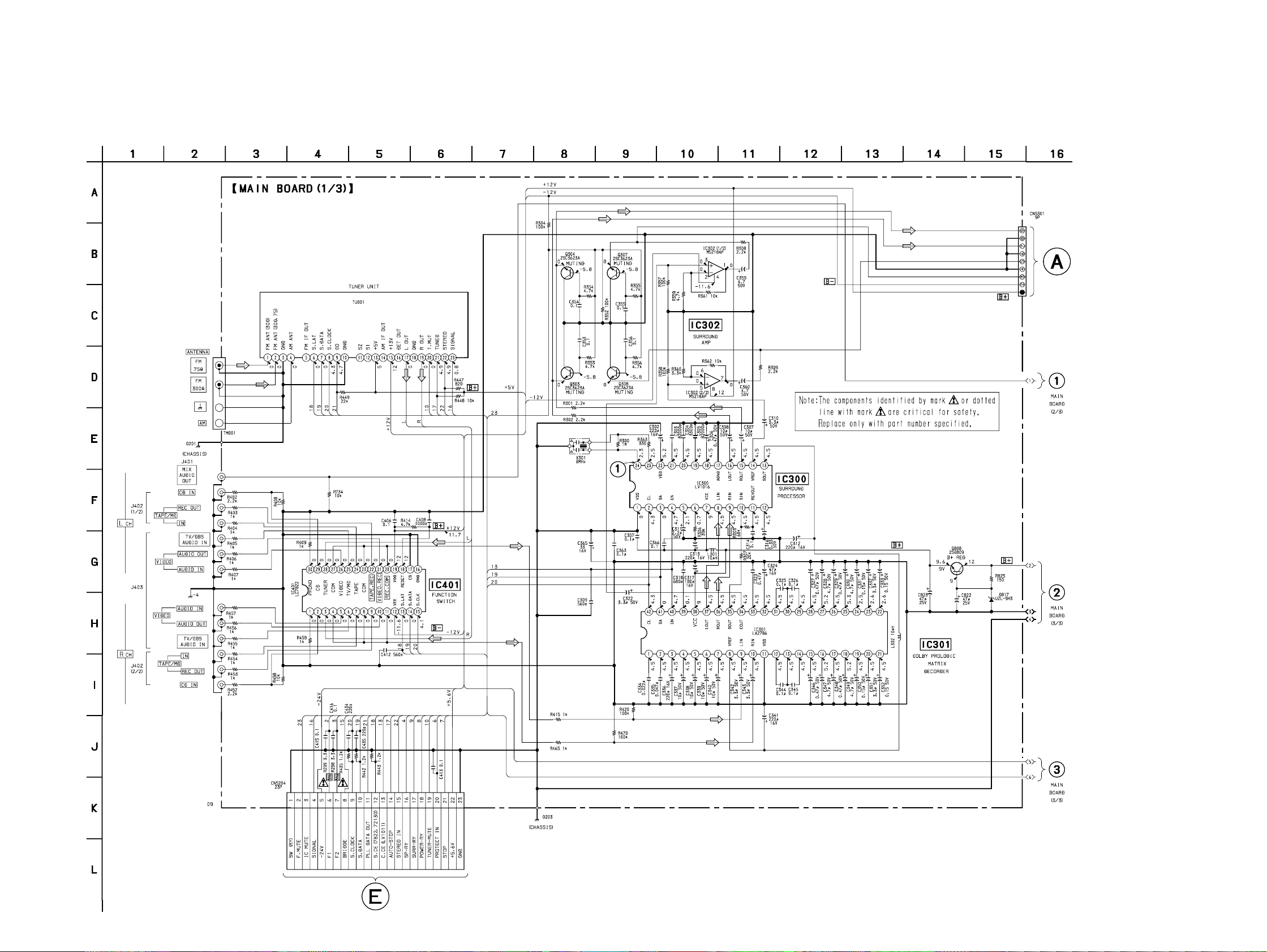
3-2. SCHEMATIC DIAGRAM – MAIN (1/3) SECTION –
• See page 6 for Waveforms.
• See page 17 for Printed Wiring Board.
• See page 33 for IC Pin Functions.
• See page 35 for IC Block Diagrams.
STR-V200
(Page 15)
(Page 9)
(Page 11)
– 7 –
(Page 11)
(Page 13)
– 8 –
Page 8
STR-V200
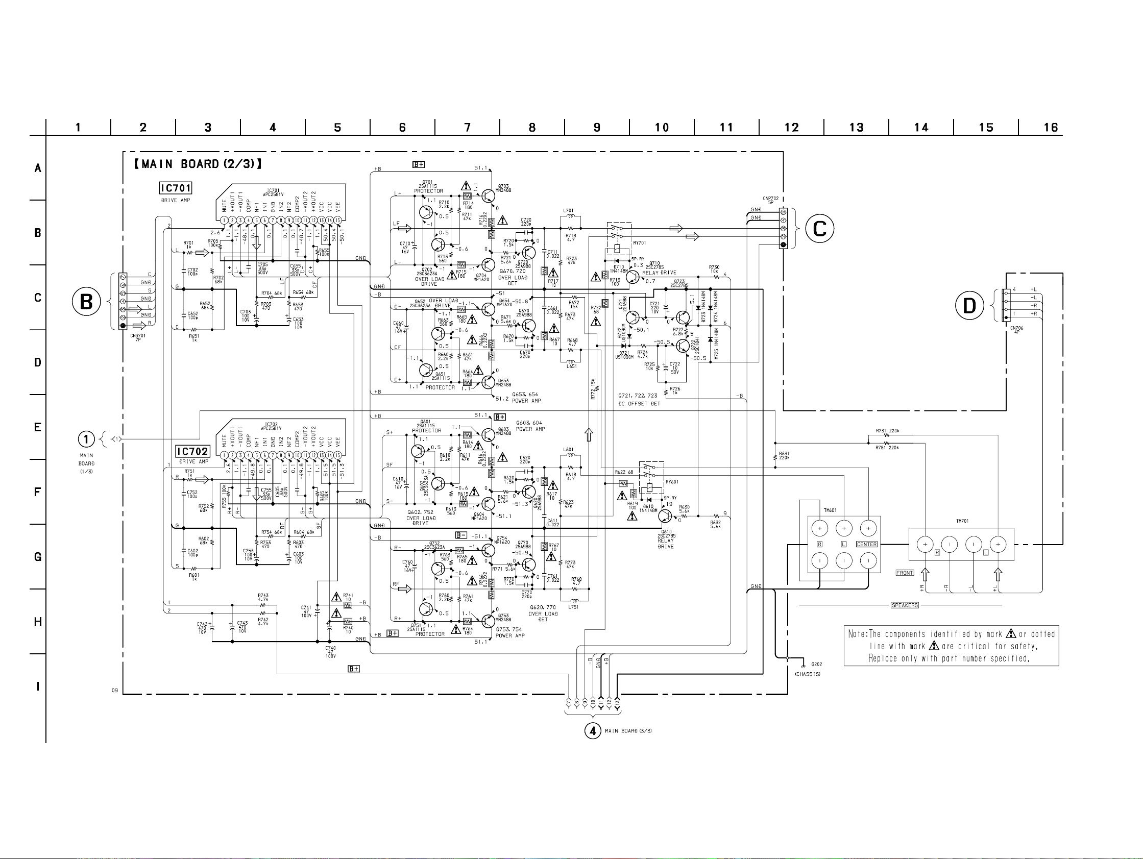
3-3. SCHEMATIC DIAGRAM – MAIN (2/3) SECTION –
• See page 17 for Printed Wiring Board.
• See page 35 for IC Block Diagrams.
(Page 16)
(Page 16)
(Page 8)
(Page 16)
(Page 11)
– 9 – – 10 –
Page 9
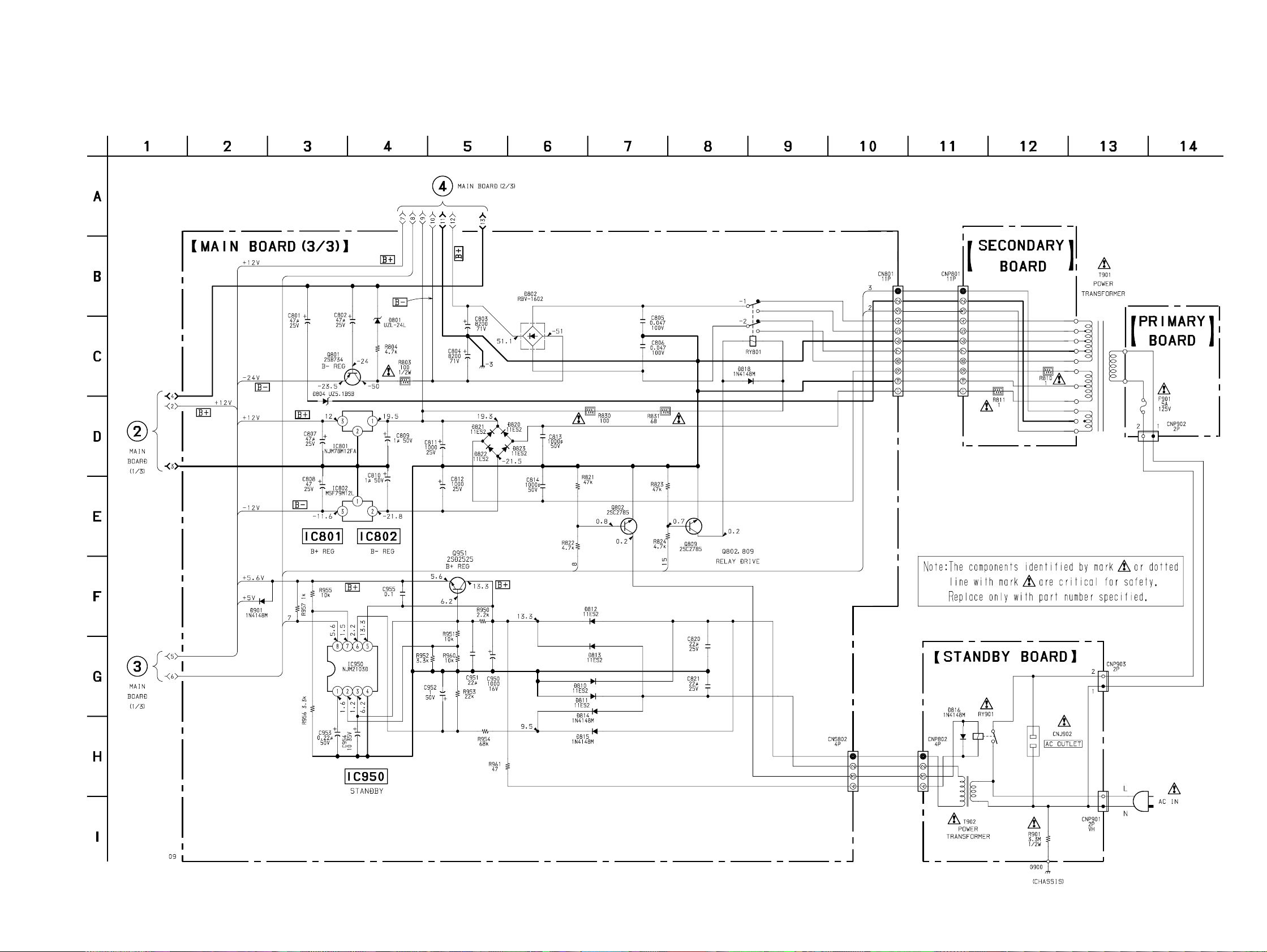
3-4. SCHEMATIC DIAGRAM – MAIN (3/3) SECTION –
• See page 17 for Printed Wiring Board.
• See page 35 for IC Block Diagrams.
STR-V200
(Page 10)
(Page 8)
(Page 8)
– 11 – – 12 –
Page 10
STR-V200
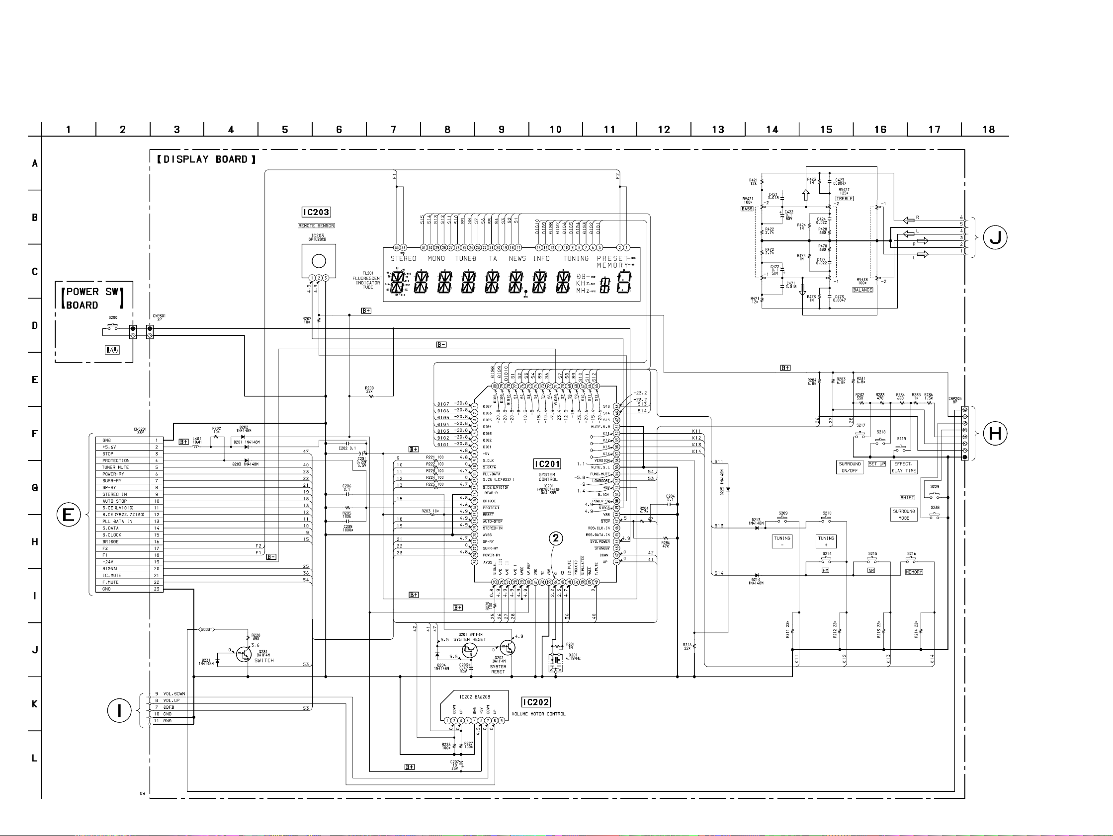
3-5. SCHEMATIC DIAGRAM – DISPLAY SECTION –
• See page 6 for Waveforms.
• See page 25 for Printed Wiring Board.
• See page 35 for IC Block Diagrams.
(Page 16)
(Page 7)
(Page 16)
(Page 15)
– 13 – – 14 –
Page 11

3-6. SCHEMATIC DIAGRAM – PANEL SECTION –
(Page 13)
(Page 8) (Page 9)
(Page 14)
(Page 14)
(Page 10)
(Page 10)
• See page 31 for Printed Wiring Board.
STR-V200
– 15 – – 16 –
Page 12

STR-V200
3-7. PRINTED WIRING BOARD – MAIN SECTION –
• See page 6 for Circuit Boards Location.
(Conductor Side)
Note: Conductor side equal an inversion of component side.
• Semiconductor
Location
Ref. No. Location
D610 B-4
D710 I-3
D721 I-9
D722 I-9
D723 I-7
D724 I-8
D725 I-8
D801 J-6
D802 E-1
D804 I-1
D810 B-1
D811 B-1
D812 B-1
D813 B-1
D814 A-1
D815 A-1
D817 D-9
D818 C-1
D820 C-2
D821 C-2
D822 B-2
D823 B-2
D901 E-9
IC300 G-8
IC301 E-8
IC302 I-8
IC401 B-8
IC701 H-6
IC702 D-6
IC801 C-8
IC802 D-8
IC950 B-3
Q303 F-10
Q304 F-9
Q307 H-9
Q308 I-9
Q601 D-6
Q602 C-5
Q603 D-5
Q604 C-5
Q610 B-3
Q620 C-6
Q651 G-6
Q652 G-5
Q653 H-5
Q654 F-5
Q670 G-6
Q701 I-6
Q702 I-5
Q703 H-5
Q704 H-5
Q710 J-3
Q720 H-6
Q721 I-8
Q722 J-8
Q723 I-8
Q751 E-6
Q752 E-5
Q753 F-5
Q754 E-5
Q770 D-6
Q801 J-7
Q802 B-1
Q808 C-9
Q809 C-1
Q951 B-3
– 17 –
– 18 –
Page 13

(Component Side)
STR-V200
– 19 – – 20 –
Page 14

STR-V200
3-8. PRINTED WIRING BOARD – POWER SECTION –
• See page 6 for Circuit Boards Location.
(Conductor Side)
Note: Conductor side equal an inversion
of component side.
– 21 –
– 22 –
Page 15

(Component Side)
STR-V200
– 23 – – 24 –
Page 16

STR-V200
3-9. PRINTED WIRING BOARD – DISPLAY SECTION –
• See page 6 for Circuit Boards Location.
(Conductor Side)
Note: Conductor side equal an inversion
of component side.
– 25 – – 26 –
Page 17

(Component Side)
STR-V200
– 27 – – 28 –
Page 18

STR-V200
3-10. PRINTED WIRING BOARD – KEY SECTION –
• See page 6 for Circuit Boards Location.
(Conductor Side)
Note: Conductor side equal an inversion
of component side.
(Component Side)
– 29 –
– 30 –
Page 19

STR-V200
3-11. PRINTED WIRING BOARD – PANEL SECTION –
• See page 6 for Circuit Boards Location.
(Conductor Side)
Note: Conductor side equal an inversion
of component side.
(Component Side)
– 31 – – 32 –
Page 20

3-12. IC PIN FUNCTIONS
• IC201 uPD78044FGF-064-3B9
Pin No.
1
2
3
4
5
6
7
8
9
10
11
12
13
14
15
16
17
18
19
20
21
22
23
24
25
26
27
28
29
30
31
32
33
34
35
36
37
38
39
40
Pin Name I/O Function
DIG7
DIG6
DIG5
DIG4
DIG3
DIG2
DIG1
+5V
S. CLK
S. DATA
PLL. DATA
S. CE (LC7288)
S. CE (LV1010)
REAR-R
BRIDGE
PROTECT
RESET
AUTO-STOP
STEREO-IN
AVSS
SP-RY
SURR-RY
POWER-RY
AVSS
SIGNAL
A/D3
A/D2
A/D1
AVDD
AV. REF
GND
NC
VSS
X1
X2
IC. MUTE
PROLOGIC
SIMULATED
HALL
T. MUTE
O
O
O
O
Fluorescent indicator tube drive
O
O
O
Power supply (+5V)
—
I
System clock
I
System data
PLL data input from TU001
I
O
Chip enable output
Chip enable output
O
I
Input for model select (Connected to ground)
I
Protector detect input
Protector detect input
I
I
System reset terminal
Auto stop detect input
I
I
Stereo detect input
—
Ground (Not used)
Speaker relay drive
O
O
Surround Relay
Power relay drive
O
—
Ground
A/D signal input terminal
I
A/D3 key input terminal
I
I
A/D2 key input terminal
A/D1 key input terminal
I
—
Power supply (+5V)
Reference voltage (+5V)
—
Ground
—
—
Not used (Open)
Ground
—
I
System clock (4.19MHz)
System clock (4.19MHz)
O
Mute drive output for µPD2581V (IC701)
O
O
Plologic LED (Not used)
CINEMA STUDIO LED (Not used)
O
O
HALL LED (Not used)
Tuner mute drive output
O
Pin No.
41
42
43
44
45
46
47
48
49
50
51
52
53
54
55
56
57
58
59
60
61
62
63
64
65
66
67
68
69
70
71
72
73
74
75
76
77
78
79
80
Pin Name I/O Function
O
VOLUME UP
VOLUME DOWN
STANDBY
SYS. POWER
RDS. DATA. IN
RDS. CLK. IN
STOP
VSS
SIRCS
POWER SW
5.1ch LED
+5V
BASS BOOST
FUNC. MUTE
SL MUTE
VERSION
K14
K13
K12
K11
SR MUTE
S15
S14
S13
S12
S11
S10
S9
S8
S7
VLOAD
S6
S5
S4
S3
S2
S1
DIG10
DIG9
DIG8
Volume up
O
Volume down
O
Standby LED drive (Not used)
I
System power ON/OFF
RDS data input (Not used)
I
I
RDS clock input (Not used)
I
Stop signal input from NJM2103D (IC950)
—
Ground
I
Sircs signal input
Power switch input terminal
I
—
5.1ch LED drive
—
Power supply (+5V)
I
Bass boost LED drive
O
Line mute drive
SL mute drive
O
I
Input for model select
I
Key in 4
I
Key in 3
I
Key in 2
Key in 1
I
O
SR mute drive
O
Not used
O
O
O
O
Fluorescent indicator tube drive
O
O
O
O
—
Connect to –24V
O
O
O
Fluorescent indicator tube drive
O
O
O
O
O
Fluorescent indicator tube drive
O
– 33 –
– 34 –
Page 21

6-13. IC BLOCK DIAGRAMS
• Main section
IC300 LV1016
1
D.GND
OSC
2 3
CLK
A
DEC
DATA
B
4
OSC
2324
VDD
IN-FILTER
(40kHz)
ENABLE
5 6
NR-DET
VDD
22
NR-IREF
20 19 18 17 16 15 14 13
21
ADM
ADM-CONT SRAM
A
B
A
7
VCC
8
L-IN
DC-CUT
B
A
–
L–R
+
L+R
(–6dB)
B
A
9 10 12
R-IN
A.GND
L-OUT
A
B
+
L+DELAY
OUT-FILTER
(7k/5k)
B-NR
B
S-IN
R-OUT
A
+
R+DELAY
DC-OUT
VREF
S-OUT
B
INV-PHASE
VOL/MUTE
S-TRIM
A
B
11
DELAY-OUT
DC-CUT
IC401 LC7822
1
IN
2
3
OUT
4
5
IN
6
7
OUT
8
9
IN
10
OUT
11
12
VEE
CE
13
DI
14
CL
15
CONTROL
IC701, 702 uPC2581
LEVEL SHIFT
LATCH
SHIFT RESISTOR
IC950 NJM2103D
30
IN
29
CR
VSC
OUTC
GND
1
2
+
–
3
4
VREF
Q
R S
+
–
28
OUT
27
26
25
IN
24
OUT
23
22
IN
IN
21
20
OUT
19
VDD
RESET
18
17
S
VSS
16
8
RESET
+
–
VSA
7
6
VSB/SESIN
V+
5
+
–
BIAS CIRCUIT
PROTECTOR
–VOUT1
COMP1
PRE
DRIVE
NF1
REG DRIVE
1
2 3 4 5 6 7 8 9 10 11 12 13 14 15
MUTE
+VOUT1
IN1
GND
PRE
DRIVE
IN2
NF2
COMP2
DRIVE
–VOUT2
+VOUT2
VCC1
VEE
VCC2
– 35 –
Page 22

IC301 LA2786
BPF1
BPF2
VREF
S-CH DC OUT
C-CH DC OUT
L-CH DC OUT
R-CH DC OUT
VREF
L-IN
R-IN
V
L-BPF1
L-BPF2
L-BPF3
1
NOISE
FILTER
2
3
V REF
4
5
6
7
8
9
10
SS
11
12
13
14
BALANCE
CONTROL
CONTROL
VR
P. S.P. S.
NOISE
CH
VR
VR
VCAVCA
VCAVCA
VCAVCA
VCAVCA
LPF
LPF
LPF
+
GENERATOR
DIVIDER
CMODE
NOISE
MUTE
+
OSC
CTRIM
CONTROL
CLK
42
41
DATA
ENABLE
40
OSC1
39
38
V
CC
L-OUT
37
R-OUT
36
S-OUT
35
34
C-OUT
CMODE-CAP.
33
C-TRIM DC CUT
32
R-BPF1
31
R-BPF2
30
R-BPF3
29
DC CUT
DC CUT
R RECT
L RECT
VLR-TH
VLR-1
VLR-2
15
16
17
18
19
20
21
RECT RECT RECT RECT
• Display section
IC202 BA6208
SWITCH
SWITCH
REG
1 2 3 4 5 6 7
NC
INPUT 1
INPUT 2
NC
GND
LOG
DIFF
MOTOR
DRIVE
MOTOR
DRIVE
Vcc
DUAL T
CONTROL
OUTPUT 2
8
OUTPUT1
LOG
DIFF
28
DC CUT
27
DC CUT
L-R RECT
26
25
L+R RECT
24
VCS-TH
VCS-1
23
VCS-2
22
9
NC
– 36 –
Page 23

SECTION 4
EXPLODED VIEWS
NOTE:
• Items marked “*” are not stocked since they are
seldom required for routine service. Some delay
should be anticipated when ordering these items.
• The mechanical parts with no reference number in
the exploded views are not supplied.
• Hardware (# mark) list and accessories and packing
materials are given in the last of this parts list.
4-1. CASE SECTION
11
10
15
FL201
The components identified by
mark ! or dotted line with mark
! are critical for safety.
Replace only with part number
specified.
17
17
18
3
3
13
14
17
12
16
3
15
3
7
8
9
Supplied
with RV404
2
1
Ref. No. Part No. Description Remark Ref. No. Part No. Description Remark
1 A-4411-215-A KNOB ASSY
2 4-210-373-01 KNOB (EQ)
3 4-951-620-01 SCREW (2.6X8), +BVTP
* 4 4-978-398-21 CUSHION
5 4-977-593-01 RING (DIA. 50), ORNAMENTAL
5
4
#2
6
* 11 1-670-378-11 POWER SW BOARD
* 12 A-4414-896-A VOL-TONE BOARD
13 1-782-074-11 WIRE (FLAT TYPE) (7 CORE)
14 1-782-075-11 WIRE (FLAT TYPE) (9 CORE)
* 15 4-921-941-01 CUSHION (FL)
6 A-4411-214-A PANEL ASSY, FRONT
7 4-996-698-41 EMBLEM, SONY
* 8 A-4414-899-A KEY BOARD
9 1-782-100-11 WIRE (FLAT TYPE) (23 CORE)
* 10 A-4414-898-A DISPLAY BOARD, COMPLETE
* 16 4-210-383-01 HOLDER (FL TUBE)
17 3-704-366-31 SCREW (CASE) (M3X6)
* 18 4-210-365-01 CASE
FL201 1-517-662-11 INDICATOR TUBE, FLUORESCENT
– 37 –
Page 24

4-2. CHASSIS SECTION
2
56
57
53
T901
not supplied
#2
not supplied
54
57
55
56
#2
#2
Q704
Q703
Q654
Q653
Q753
56
not
supplied
Q754
Q603
58
62
Q604
59
#2
#2
61
#2
#2
63
#2
#
not
supplied
#2
#2
60
not supplied
#2
#1
Ref. No. Part No. Description Remark Ref. No. Part No. Description Remark
51 X-4946-543-1 FOOT (SMALL) ASSY
* 52 1-670-374-11 SPEAKER SW BOARD
* 53 1-670-376-11 PRIMARY BOARD
* 54 1-670-375-11 SECONDARY BOARD
* 55 1-670-373-11 STANDBY BOARD
! 56 1-690-609-21 CORD, POWER
57 4-900-386-01 SCREW
58 4-210-380-01 RIVET, NYLON
59 3-905-609-01 SCREW (TRANSISTOR)
* 60 4-978-398-21 CUSHION
* 61 A-4414-900-A MAIN BOARD, COMPLETE
52
62 3-703-244-00 BUSHING (2104), CORD
* 63 4-210-367-01 PANEL, BACK
Q603 8-749-010-25 IC MN2488-OPY-M
Q604 8-749-010-26 IC MP1620-OPY-M
Q653 8-749-010-25 IC MN2488-OPY-M
Q654 8-749-010-26 IC MP1620-OPY-M
Q703 8-749-010-25 IC MN2488-OPY-M
Q704 8-749-010-26 IC MP1620-OPY-M
Q753 8-749-010-25 IC MN2488-OPY-M
Q754 8-749-010-26 IC MP1620-OPY-M
! T901 1-431-258-11 TRANSFORMER, POWER
51
The components identified by mark ! or dotted
line with mark ! are critical for safety.
Replace only with part number specified.
– 38 –
Page 25

SECTION 5
ELECTRICAL PARTS LIST
Note:
The components identified by
mark ! or dotted line with mark
! are critical for safety.
Replace only with part number
specified.
When indicating parts by reference
number, please include the board
name.
Ref. No. Part No. Description Remark Ref. No. Part No. Description Remark
* A-4414-899-A KEY BOARD, COMPLETE
********************
• Due to standardization, replacements in the parts list
may be different from the parts specified in the
diagrams or the components used on the set.
• -XX, -X mean standardized parts, so they may have
some difference from the original one.
• Items marked “*” are not stocked since they are
seldom required for routine service. Some delay
should be anticipated when ordering these items.
• RESIST ORS
All resistors are in ohms
METAL: Metal-film resistor
METAL OXIDE: Metal Oxide-film resistor
F : nonflammable
* A-4414-898-A DISPLAY BOARD, COMPLETE
• SEMICONDUCTORS
In each case, u: µ , for example:
uA...: µ A..., uPA...: µ PA..., uPB...: µ PB...,
uPC...: µ PC..., uPD...: µ PD...
• CAPACITORS
uF : µ F
• COILS
uH : µ H
***********************
KEY
DISPLAY
< CONNECTOR >
* CNS205 1-580-169-11 PIN, CONNECTOR (PC BOARD) 8P
< DIODE >
D238 8-719-070-78 DIODE SEL6810A-TP6 (BASS BOOST)
< RESISTOR >
R237 1-249-421-11 CARBON 2.2K 5% 1/4W F
R238 1-247-843-11 CARBON 3.3K 5% 1/4W
R239 1-249-411-11 CARBON 330 5% 1/4W
R240 1-249-413-11 CARBON 470 5% 1/4W F
R241 1-249-415-11 CARBON 680 5% 1/4W F
R242 1-249-417-11 CARBON 1K 5% 1/4W F
R243 1-249-419-11 CARBON 1.5K 5% 1/4W F
R244 1-249-426-11 CARBON 5.6K 5% 1/4W
R246 1-249-411-11 CARBON 330 5% 1/4W
R247 1-249-413-11 CARBON 470 5% 1/4W F
R248 1-249-415-11 CARBON 680 5% 1/4W F
R249 1-249-417-11 CARBON 1K 5% 1/4W F
R280 1-249-419-11 CARBON 1.5K 5% 1/4W F
R281 1-249-421-11 CARBON 2.2K 5% 1/4W F
R282 1-247-843-11 CARBON 3.3K 5% 1/4W
< SWITCH >
S221 1-554-937-11 SWITCH, KEY BOARD (CD)
S222 1-554-937-11 SWITCH, KEY BOARD (TUNER)
S223 1-554-937-11 SWITCH, KEY BOARD (VIDEO)
S224 1-554-937-11 SWITCH, KEY BOARD (6)
S225 1-554-937-11 SWITCH, KEY BOARD (7)
S226 1-554-937-11 SWITCH, KEY BOARD (8)
S227 1-554-937-11 SWITCH, KEY BOARD (9)
S228 1-554-937-11 SWITCH, KEY BOARD (0)
S231 1-554-937-11 SWITCH, KEY BOARD (TV/DBS)
S232 1-554-937-11 SWITCH, KEY BOARD (1)
S233 1-554-937-11 SWITCH, KEY BOARD (2)
S234 1-554-937-11 SWITCH, KEY BOARD (3)
S235 1-554-937-11 SWITCH, KEY BOARD (4)
S236 1-554-937-11 SWITCH, KEY BOARD (5)
S237 1-554-937-11 SWITCH, KEY BOARD (DIRECT)
S239 1-554-937-11 SWITCH, KEY BOARD (TAPE/MD)
**************************************************************
* 4-210-383-01 HOLDER (FL TUBE)
* 4-921-941-01 CUSHION (FL)
< CAPACITOR >
C201 1-104-905-11 CAPACITOR 0.22F 5.5V
C202 1-164-159-21 CERAMIC 0.1uF 50V
C203 1-124-465-00 ELECT 0.47uF 20% 50V
C204 1-164-159-21 CERAMIC 0.1uF 50V
C205 1-162-294-31 CERAMIC 0.001uF 10% 50V
C206 1-164-159-21 CERAMIC 0.1uF 50V
C207 1-126-096-11 ELECT 10uF 20% 35V
C421 1-137-440-11 FILM 0.018uF 5% 50V
C422 1-124-463-00 ELECT 0.1uF 20% 50V
C423 1-137-368-11 FILM 0.0047uF 5% 50V
C424 1-137-372-11 FILM 0.022uF 5% 50V
C471 1-137-440-11 FILM 0.018uF 5% 50V
C472 1-124-463-00 ELECT 0.1uF 20% 50V
C473 1-137-368-11 FILM 0.0047uF 5% 50V
C474 1-137-372-11 FILM 0.022uF 5% 50V
< CONNECTOR >
* CNP205 1-580-160-11 PIN, CONNECTOR (PC BOARD) 8P
CNP301 1-566-690-11 PLUG, CONNECTOR (2.5MM) 2P
CNS201 1-568-742-11 SOCKET, CONNECTOR 23P
< DIODE >
D201 8-719-911-19 DIODE 1SS119-25
D202 8-719-911-19 DIODE 1SS119-25
D203 8-719-911-19 DIODE 1SS119-25
D204 8-719-911-19 DIODE 1SS119-25
D213 8-719-911-19 DIODE 1SS119-25
D214 8-719-911-19 DIODE 1SS119-25
D225 8-719-911-19 DIODE 1SS119-25
D231 8-719-911-19 DIODE 1SS119-25
< FLUORESCENT INDICATOR >
FL201 1-517-141-11 INDICATOR TUBE, FLUORESCENT
< IC >
IC201 8-759-479-19 IC uPD78044FGF-064-3B9
IC202 8-759-962-08 IC BA6208
IC203 8-759-339-53 IC GP1U28XB
– 39 –
Page 26

DISPLAY MAIN
Ref. No. Part No. Description Remark Ref. No. Part No. Description Remark
< COIL >
L401 1-410-509-11 INDUCTOR 10uH
< TRANSISTOR >
Q201 8-729-900-63 TRANSISTOR DTA124ES
Q202 8-729-900-36 TRANSISTOR DTC124ES
Q231 8-729-900-36 TRANSISTOR DTC124ES
< RESISTOR >
R200 1-247-863-91 CARBON 22K 5% 1/4W
R201 1-247-903-00 CARBON 1M 5% 1/4W
R202 1-249-429-11 CARBON 10K 5% 1/4W
R203 1-249-429-11 CARBON 10K 5% 1/4W
R204 1-249-425-11 CARBON 4.7K 5% 1/4W F
R205 1-249-441-11 CARBON 100K 5% 1/4W
R207 1-249-429-11 CARBON 10K 5% 1/4W
R211 1-247-863-91 CARBON 22K 5% 1/4W
R212 1-247-863-91 CARBON 22K 5% 1/4W
R213 1-247-863-91 CARBON 22K 5% 1/4W
S210 1-554-937-11 SWITCH, KEY BOARD (TUNING +)
S214 1-554-937-11 SWITCH, KEY BOARD (FM)
S215 1-554-937-11 SWITCH, KEY BOARD (AM)
S216 1-554-937-11 SWITCH, KEY BOARD (MEMORY)
S217 1-554-937-11 SWITCH, KEY BOARD (SURROUND ON/OFF)
S218 1-554-937-11 SWITCH, KEY BOARD (SET UP)
S219 1-554-937-11 SWITCH, KEY BOARD (EFFECT, DELAY TIME)
S229 1-554-937-11 SWITCH, KEY BOARD (SHIFT)
S238 1-554-937-11 SWITCH, KEY BOARD (SURROUND MODE)
< VIBRATOR >
X201 1-577-101-11 VIBRATOR, CERAMIC (4.19MHz)
**************************************************************
* A-4414-900-A MAIN BOARD, COMPLETE
********************
3-905-609-01 SCREW (TRANSISTOR)
4-210-380-01 RIVET, NYLON
7-685-872-09 SCREW +BVTT 3X8 (S)
R214 1-247-863-91 CARBON 22K 5% 1/4W
R216 1-247-863-91 CARBON 22K 5% 1/4W
R221 1-247-807-31 CARBON 100 5% 1/4W
R222 1-247-807-31 CARBON 100 5% 1/4W
R223 1-247-807-31 CARBON 100 5% 1/4W
R224 1-247-807-31 CARBON 100 5% 1/4W
R225 1-247-807-31 CARBON 100 5% 1/4W
R226 1-249-441-11 CARBON 100K 5% 1/4W
R227 1-249-441-11 CARBON 100K 5% 1/4W
R228 1-249-412-11 CARBON 390 5% 1/4W F
R231 1-249-427-11 CARBON 6.8K 5% 1/4W F
R232 1-249-411-11 CARBON 330 5% 1/4W
R233 1-249-413-11 CARBON 470 5% 1/4W F
R234 1-249-415-11 CARBON 680 5% 1/4W F
R235 1-249-417-11 CARBON 1K 5% 1/4W F
R236 1-249-419-11 CARBON 1.5K 5% 1/4W F
R270 1-247-807-31 CARBON 100 5% 1/4W
R283 1-249-427-11 CARBON 6.8K 5% 1/4W F
R284 1-249-427-11 CARBON 6.8K 5% 1/4W F
R286 1-249-437-11 CARBON 47K 5% 1/4W
R420 1-249-415-11 CARBON 680 5% 1/4W F
R421 1-249-430-11 CARBON 12K 5% 1/4W
R422 1-249-422-11 CARBON 2.7K 5% 1/4W F
R423 1-247-903-00 CARBON 1M 5% 1/4W
R424 1-247-903-00 CARBON 1M 5% 1/4W
R470 1-249-415-11 CARBON 680 5% 1/4W F
R471 1-249-430-11 CARBON 12K 5% 1/4W
R472 1-249-422-11 CARBON 2.7K 5% 1/4W F
R473 1-247-903-00 CARBON 1M 5% 1/4W
R474 1-247-903-00 CARBON 1M 5% 1/4W
< VARIABLE RESISTOR >
< CAPACITOR >
C302 1-126-934-11 ELECT 220uF 20% 16V
C303 1-130-494-11 MYLAR 0.082uF 5% 50V
C304 1-137-367-11 FILM 0.0033uF 5% 50V
C305 1-130-494-11 MYLAR 0.082uF 5% 50V
C306 1-126-959-11 ELECT 0.47uF 20% 50V
C307 1-126-964-11 ELECT 10uF 20% 50V
C308 1-126-964-11 ELECT 10uF 20% 50V
C309 1-162-291-31 CERAMIC 560PF 10% 50V
C310 1-126-962-11 ELECT 3.3uF 20% 50V
C311 1-126-961-11 ELECT 2.2uF 20% 50V
C312 1-126-934-11 ELECT 220uF 20% 16V
C313 1-126-934-11 ELECT 220uF 20% 16V
C314 1-136-165-00 FILM 0.1uF 5% 50V
C316 1-124-252-00 ELECT 0.33uF 20% 50V
C317 1-126-933-11 ELECT 100uF 20% 16V
C318 1-136-357-11 FILM 680PF 5% 50V
C322 1-126-962-11 ELECT 3.3uF 20% 50V
C323 1-136-173-00 FILM 0.47uF 5% 50V
C324 1-126-967-11 ELECT 47uF 20% 16V
C325 1-136-165-00 FILM 0.1uF 5% 50V
C326 1-136-165-00 FILM 0.1uF 5% 50V
C327 1-126-959-11 ELECT 0.47uF 20% 50V
C328 1-126-963-11 ELECT 4.7uF 20% 50V
C329 1-126-959-11 ELECT 0.47uF 20% 50V
C330 1-126-963-11 ELECT 4.7uF 20% 50V
C331 1-124-250-11 ELECT 0.15uF 20% 50V
C332 1-126-962-11 ELECT 3.3uF 20% 50V
C333 1-124-250-11 ELECT 0.15uF 20% 50V
C334 1-137-372-11 FILM 0.022uF 5% 50V
C335 1-136-161-00 FILM 0.047uF 5% 50V
RV421 1-225-660-11 RES, VAR 100K/100K (BASS)
RV422 1-225-659-11 RES, VAR 125K/125K (TREBLE)
RV423 1-225-658-11 RES, VAR 100K/100K (BALANCE)
< SWITCH >
S209 1-554-937-11 SWITCH, KEY BOARD (TUNING –)
C336 1-126-934-11 ELECT 220uF 20% 16V
C337 1-126-964-11 ELECT 10uF 20% 50V
C338 1-126-964-11 ELECT 10uF 20% 50V
C339 1-126-964-11 ELECT 10uF 20% 50V
C340 1-126-964-11 ELECT 10uF 20% 50V
C341 1-126-934-11 ELECT 220uF 20% 16V
– 40 –
Page 27

MAIN
Ref. No. Part No. Description Remark Ref. No. Part No. Description Remark
C342 1-126-962-11 ELECT 3.3uF 20% 50V
C343 1-126-962-11 ELECT 3.3uF 20% 50V
C344 1-136-165-00 FILM 0.1uF 5% 50V
C345 1-136-165-00 FILM 0.1uF 5% 50V
C346 1-126-959-11 ELECT 0.47uF 20% 50V
C347 1-126-963-11 ELECT 4.7uF 20% 50V
C348 1-126-959-11 ELECT 0.47uF 20% 50V
C349 1-126-963-11 ELECT 4.7uF 20% 50V
C350 1-124-250-11 ELECT 0.15uF 20% 50V
C351 1-126-962-11 ELECT 3.3uF 20% 50V
C352 1-124-250-11 ELECT 0.15uF 20% 50V
C353 1-164-159-21 CERAMIC 0.1uF 50V
C354 1-164-159-21 CERAMIC 0.1uF 50V
C355 1-164-159-21 CERAMIC 0.1uF 50V
C356 1-164-159-21 CERAMIC 0.1uF 50V
C357 1-164-159-21 CERAMIC 0.1uF 50V
C359 1-126-963-11 ELECT 4.7uF 20% 50V
C360 1-126-963-11 ELECT 4.7uF 20% 50V
C363 1-164-159-21 CERAMIC 0.1uF 50V
C365 1-126-966-11 ELECT 33uF 20% 16V
C366 1-164-159-21 CERAMIC 0.1uF 50V
C406 1-164-159-21 CERAMIC 0.1uF 50V
C408 1-162-294-31 CERAMIC 0.001uF 10% 50V
C412 1-162-291-31 CERAMIC 560PF 10% 50V
C413 1-164-159-21 CERAMIC 0.1uF 50V
C415 1-164-159-21 CERAMIC 0.1uF 50V
C416 1-164-159-21 CERAMIC 0.1uF 50V
C434 1-162-286-21 CERAMIC 220PF 10% 50V
C435 1-162-286-21 CERAMIC 220PF 10% 50V
C602 1-162-282-31 CERAMIC 100PF 10% 50V
C603 1-104-665-11 ELECT 100uF 20% 10V
C605 1-102-233-00 CERAMIC 33PF 10% 500V
C610 1-126-967-11 ELECT 47uF 20% 16V
C611 1-137-372-11 FILM 0.022uF 5% 50V
C770 1-162-286-21 CERAMIC 220PF 10% 50V
C801 1-104-664-11 ELECT 47uF 20% 25V
C802 1-104-664-11 ELECT 47uF 20% 25V
C803 1-107-766-11 ELECT(BLOCK) 8200uF 20% 71V
C804 1-107-766-11 ELECT(BLOCK) 8200uF 20% 71V
C805 1-137-420-11 FILM 0.047uF 10% 100V
C806 1-137-420-11 FILM 0.047uF 10% 100V
C807 1-104-664-11 ELECT 47uF 20% 25V
C808 1-104-664-11 ELECT 47uF 20% 25V
C809 1-126-960-11 ELECT 1uF 20% 50V
C810 1-126-960-11 ELECT 1uF 20% 50V
C811 1-126-942-61 ELECT 1000uF 20% 25V
C812 1-126-942-61 ELECT 1000uF 20% 25V
C813 1-101-001-00 CERAMIC 0.001uF 50V
C814 1-101-001-00 CERAMIC 0.001uF 50V
C820 1-161-494-00 CERAMIC 0.022uF 25V
C821 1-161-494-00 CERAMIC 0.022uF 25V
C822 1-104-664-11 ELECT 47uF 20% 25V
C823 1-104-664-11 ELECT 47uF 20% 25V
C950 1-126-767-11 ELECT 1000uF 20% 16V
C951 1-164-097-11 CERAMIC 0.022uF 50V
C952 1-126-960-11 ELECT 1uF 20% 50V
C953 1-124-464-11 ELECT 0.22uF 20% 50V
C954 1-126-096-11 ELECT 10uF 20% 35V
C955 1-164-159-21 CERAMIC 0.1uF 50V
< CONNECTOR >
* CN706 1-764-321-11 PIN, CONNECTOR (PC BOARD) 4P
CNP702 1-764-474-11 PIN, CONNECTOR (PC BOARD) 5P
CNS204 1-568-742-11 SOCKET, CONNECTOR 23P
CNS301 1-568-442-11 SOCKET, CONNECTOR 9P
CNS701 1-568-439-11 SOCKET, CONNECTOR 7P
* CNS802 1-564-778-11 PLUG, CONNECTOR (2.5MM) 4P
C620 1-162-286-21 CERAMIC 220PF 10% 50V
C652 1-162-282-31 CERAMIC 100PF 10% 50V
C653 1-104-665-11 ELECT 100uF 20% 10V
C655 1-102-233-00 CERAMIC 33PF 10% 500V
C660 1-126-967-11 ELECT 47uF 20% 16V
C661 1-137-372-11 FILM 0.022uF 5% 50V
C670 1-162-286-21 CERAMIC 220PF 10% 50V
C702 1-162-282-31 CERAMIC 100PF 10% 50V
C703 1-104-665-11 ELECT 100uF 20% 10V
C705 1-102-233-00 CERAMIC 33PF 10% 500V
C710 1-126-967-11 ELECT 47uF 20% 16V
C711 1-137-372-11 FILM 0.022uF 5% 50V
C720 1-162-286-21 CERAMIC 220PF 10% 50V
C721 1-126-934-11 ELECT 220uF 20% 10V
C722 1-126-964-11 ELECT 10uF 20% 50V
C740 1-128-562-11 ELECT 47uF 20% 100V
C741 1-128-562-11 ELECT 47uF 20% 100V
C742 1-126-925-11 ELECT 470uF 20% 10V
C743 1-126-925-11 ELECT 470uF 20% 10V
C752 1-162-282-31 CERAMIC 100PF 10% 50V
C753 1-104-665-11 ELECT 100uF 20% 10V
C755 1-102-233-00 CERAMIC 33PF 10% 500V
C760 1-126-967-11 ELECT 47uF 20% 16V
C761 1-137-372-11 FILM 0.022uF 5% 50V
< DIODE >
D610 8-719-911-19 DIODE 1SS119-25
D710 8-719-911-19 DIODE 1SS119-25
D721 8-719-815-85 DIODE 1S1585
D722 8-719-815-85 DIODE 1S1585
D723 8-719-911-19 DIODE 1SS119-25
D724 8-719-911-19 DIODE 1SS119-25
D725 8-719-911-19 DIODE 1SS119-25
D801 8-719-936-37 DIODE HZS24-1LTD
D802 8-719-302-38 DIODE RBV-602-01
D804 8-719-923-38 DIODE MTZJ-T-77-5.6B
D810 8-719-200-82 DIODE 11ES2
D811 8-719-200-82 DIODE 11ES2
D812 8-719-200-82 DIODE 11ES2
D813 8-719-200-82 DIODE 11ES2
D814 8-719-911-19 DIODE 1SS119-25
D815 8-719-911-19 DIODE 1SS119-25
D817 8-719-001-30 DIODE UZL-9H3
D818 8-719-911-19 DIODE 1SS119-25
D820 8-719-200-82 DIODE 11ES2
D821 8-719-200-82 DIODE 11ES2
D822 8-719-200-82 DIODE 11ES2
D823 8-719-200-82 DIODE 11ES2
– 41 –
Page 28

MAIN
Ref. No. Part No. Description Remark Ref. No. Part No. Description Remark
D901 8-719-911-19 DIODE 1SS119-25
< EARTH >
* G201 1-537-738-21 TERMINAL, EARTH
* G202 1-537-738-21 TERMINAL, EARTH
* G203 1-537-738-21 TERMINAL, EARTH
< IC >
IC300 8-759-442-97 IC LV1016
IC301 8-759-442-96 IC LA2786
IC302 8-759-636-74 IC M5218AP-22
IC401 8-759-805-14 IC LC7822
IC701 8-759-326-52 IC uPC2581V
IC702 8-759-326-52 IC uPC2581V
IC801 8-759-231-58 IC TA7812S
IC802 8-759-604-45 IC M5F79M12L
IC950 8-759-333-83 IC NJM2103D
< JACK >
J401 1-774-843-11 JACK, PIN 1P (MIX AUDIO OUT)
J402 1-774-005-21 JACK, PIN 6P (TAPE/MD, CD)
J403 1-770-615-21 JACK, PIN 6P (VIDEO, TV/DBS)
< COIL >
L301 1-410-509-11 INDUCTOR 10uH
L302 1-410-509-11 INDUCTOR 10uH
L601 1-420-872-00 COIL, AIR-CORE
L651 1-420-872-00 COIL, AIR-CORE
L701 1-420-872-00 COIL, AIR-CORE
L751 1-420-872-00 COIL, AIR-CORE
Q752 8-729-141-30 TRANSISTOR 2SC3623A-LK
Q753 8-749-010-25 IC MN2488-OPY-M
Q754 8-749-010-26 IC MP1620-OPY-M
Q770 8-729-140-82 TRANSISTOR 2SA988-PAFAEA
Q801 8-729-140-97 TRANSISTOR 2SB734-34
Q802 8-729-119-78 TRANSISTOR 2SC2785-HFE
Q808 8-729-180-92 TRANSISTOR 2SD809-K
Q809 8-729-119-78 TRANSISTOR 2SC2785-HFE
Q951 8-729-026-68 TRANSISTOR 2SD2525(TP)
< RESISTOR >
! R298 1-249-387-11 CARBON 3.3 5% 1/4W F
! R299 1-249-387-11 CARBON 3.3 5% 1/4W F
R300 1-247-903-00 CARBON 1M 5% 1/4W
R301 1-249-421-11 CARBON 2.2K 5% 1/4W F
R302 1-249-421-11 CARBON 2.2K 5% 1/4W F
R303 1-249-439-11 CARBON 68K 5% 1/4W
R304 1-249-441-11 CARBON 100K 5% 1/4W
R306 1-249-436-11 CARBON 39K 5% 1/4W
R307 1-247-862-11 CARBON 20K 5% 1/4W
R308 1-249-421-11 CARBON 2.2K 5% 1/4W F
R309 1-249-421-11 CARBON 2.2K 5% 1/4W F
R352 1-249-441-11 CARBON 100K 5% 1/4W
R353 1-249-425-11 CARBON 4.7K 5% 1/4W F
R354 1-249-425-11 CARBON 4.7K 5% 1/4W F
R355 1-249-425-11 CARBON 4.7K 5% 1/4W F
R356 1-249-425-11 CARBON 4.7K 5% 1/4W F
R357 1-249-441-11 CARBON 100K 5% 1/4W
R358 1-249-441-11 CARBON 100K 5% 1/4W
R359 1-249-425-11 CARBON 4.7K 5% 1/4W F
R360 1-247-843-11 CARBON 3.3K 5% 1/4W
< TRANSISTOR >
Q303 8-729-141-30 TRANSISTOR 2SC3623A-LK
Q304 8-729-141-30 TRANSISTOR 2SC3623A-LK
Q307 8-729-141-30 TRANSISTOR 2SC3623A-LK
Q308 8-729-141-30 TRANSISTOR 2SC3623A-LK
Q601 8-729-119-76 TRANSISTOR 2SA1175-HFE
Q602 8-729-141-30 TRANSISTOR 2SC3623A-LK
Q603 8-749-010-25 IC MN2488-OPY-M
Q604 8-749-010-26 IC MP1620-OPY-M
Q610 8-729-119-78 TRANSISTOR 2SC2785-HFE
Q620 8-729-140-82 TRANSISTOR 2SA988-PAFAEA
Q651 8-729-119-76 TRANSISTOR 2SA1175-HFE
Q652 8-729-141-30 TRANSISTOR 2SC3623A-LK
Q653 8-749-010-25 IC MN2488-OPY-M
Q654 8-749-010-26 IC MP1620-OPY-M
Q670 8-729-140-82 TRANSISTOR 2SA988-PAFAEA
Q701 8-729-119-76 TRANSISTOR 2SA1175-HFE
Q702 8-729-141-30 TRANSISTOR 2SC3623A-LK
Q703 8-749-010-25 IC MN2488-OPY-M
Q704 8-749-010-26 IC MP1620-OPY-M
Q710 8-729-119-78 TRANSISTOR 2SC2785-HFE
Q720 8-729-140-82 TRANSISTOR 2SA988-PAFAEA
Q721 8-729-140-82 TRANSISTOR 2SA988-PAFAEA
Q722 8-729-140-84 TRANSISTOR 2SC1841-PAFAEA
Q723 8-729-119-78 TRANSISTOR 2SC2785-HFE
Q751 8-729-119-76 TRANSISTOR 2SA1175-HFE
R361 1-249-429-11 CARBON 10K 5% 1/4W
R362 1-249-429-11 CARBON 10K 5% 1/4W
R363 1-249-411-11 CARBON 330 5% 1/4W
R402 1-249-421-11 CARBON 2.2K 5% 1/4W F
R403 1-249-417-11 CARBON 1K 5% 1/4W F
R404 1-249-417-11 CARBON 1K 5% 1/4W F
R405 1-249-417-11 CARBON 1K 5% 1/4W F
R406 1-249-417-11 CARBON 1K 5% 1/4W F
R407 1-249-417-11 CARBON 1K 5% 1/4W F
R408 1-249-429-11 CARBON 10K 5% 1/4W
R409 1-249-417-11 CARBON 1K 5% 1/4W F
R414 1-249-425-11 CARBON 4.7K 5% 1/4W F
R415 1-249-417-11 CARBON 1K 5% 1/4W F
R420 1-249-441-11 CARBON 100K 5% 1/4W
R435 1-249-418-11 CARBON 1.2K 5% 1/4W F
R442 1-249-418-11 CARBON 1.2K 5% 1/4W F
R443 1-249-418-11 CARBON 1.2K 5% 1/4W F
R447 1-249-416-11 CARBON 820 5% 1/4W F
R448 1-249-429-11 CARBON 10K 5% 1/4W
R449 1-247-863-91 CARBON 22K 5% 1/4W
R452 1-249-421-11 CARBON 2.2K 5% 1/4W F
R453 1-249-417-11 CARBON 1K 5% 1/4W F
R454 1-249-417-11 CARBON 1K 5% 1/4W F
R455 1-249-417-11 CARBON 1K 5% 1/4W F
R456 1-249-417-11 CARBON 1K 5% 1/4W F
R457 1-249-417-11 CARBON 1K 5% 1/4W F
R458 1-249-429-11 CARBON 10K 5% 1/4W
– 42 –
The components identified by mark ! or dotted
line with mark ! are critical for safety.
Replace only with part number specified.
Page 29

MAIN
Ref. No. Part No. Description Remark Ref. No. Part No. Description Remark
R459 1-249-417-11 CARBON 1K 5% 1/4W F
R465 1-249-417-11 CARBON 1K 5% 1/4W F
R470 1-249-441-11 CARBON 100K 5% 1/4W
R601 1-249-417-11 CARBON 1K 5% 1/4W F
R602 1-249-439-11 CARBON 68K 5% 1/4W
R603 1-249-413-11 CARBON 470 5% 1/4W F
R604 1-249-439-11 CARBON 68K 5% 1/4W
R605 1-249-441-11 CARBON 100K 5% 1/4W
R610 1-249-421-11 CARBON 2.2K 5% 1/4W F
R611 1-249-437-11 CARBON 47K 5% 1/4W
R613 1-249-414-11 CARBON 560 5% 1/4W F
! R614 1-249-408-11 CARBON 180 5% 1/4W F
! R615 1-249-408-11 CARBON 180 5% 1/4W F
! R616 1-233-352-21 ENCAPSULATED COMPONENT
! R617 1-249-393-11 CARBON 10 5% 1/4W F
R618 1-249-389-11 CARBON 4.7 5% 1/4W F
! R619 1-249-405-11 CARBON 100 5% 1/4W F
R620 1-249-419-11 CARBON 1.5K 5% 1/4W F
R621 1-249-426-11 CARBON 5.6K 5% 1/4W
! R622 1-249-403-11 CARBON 68 5% 1/4W F
R623 1-249-437-11 CARBON 47K 5% 1/4W
R630 1-249-426-11 CARBON 5.6K 5% 1/4W
R631 1-247-887-00 CARBON 220K 5% 1/4W
R632 1-249-426-11 CARBON 5.6K 5% 1/4W
R651 1-249-417-11 CARBON 1K 5% 1/4W F
R652 1-249-439-11 CARBON 68K 5% 1/4W
R653 1-249-413-11 CARBON 470 5% 1/4W F
R654 1-249-439-11 CARBON 68K 5% 1/4W
R655 1-249-441-11 CARBON 100K 5% 1/4W
R660 1-249-421-11 CARBON 2.2K 5% 1/4W F
R661 1-249-437-11 CARBON 47K 5% 1/4W
R663 1-249-414-11 CARBON 560 5% 1/4W F
! R664 1-249-408-11 CARBON 180 5% 1/4W F
! R665 1-249-408-11 CARBON 180 5% 1/4W F
! R666 1-233-352-21 ENCAPSULATED COMPONENT
! R667 1-249-393-11 CARBON 10 5% 1/4W F
R668 1-249-389-11 CARBON 4.7 5% 1/4W F
R670 1-249-419-11 CARBON 1.5K 5% 1/4W F
R671 1-249-426-11 CARBON 5.6K 5% 1/4W
R672 1-249-431-11 CARBON 15K 5% 1/4W
R673 1-249-437-11 CARBON 47K 5% 1/4W
R701 1-249-417-11 CARBON 1K 5% 1/4W F
R702 1-249-439-11 CARBON 68K 5% 1/4W
R703 1-249-413-11 CARBON 470 5% 1/4W F
R704 1-249-439-11 CARBON 68K 5% 1/4W
R705 1-249-441-11 CARBON 100K 5% 1/4W
R710 1-249-421-11 CARBON 2.2K 5% 1/4W F
R711 1-249-437-11 CARBON 47K 5% 1/4W
R713 1-249-414-11 CARBON 560 5% 1/4W F
! R714 1-249-408-11 CARBON 180 5% 1/4W F
! R715 1-249-408-11 CARBON 180 5% 1/4W F
! R716 1-233-352-21 ENCAPSULATED COMPONENT
! R717 1-249-393-11 CARBON 10 5% 1/4W F
R718 1-249-389-11 CARBON 4.7 5% 1/4W F
! R719 1-249-405-11 CARBON 100 5% 1/4W F
R720 1-249-419-11 CARBON 1.5K 5% 1/4W F
R721 1-249-426-11 CARBON 5.6K 5% 1/4W
! R722 1-249-403-11 CARBON 68 5% 1/4W F
R723 1-249-437-11 CARBON 47K 5% 1/4W
R724 1-249-425-11 CARBON 4.7K 5% 1/4W F
R725 1-249-429-11 CARBON 10K 5% 1/4W
R726 1-249-417-11 CARBON 1K 5% 1/4W F
R727 1-249-427-11 CARBON 6.8K 5% 1/4W F
R730 1-249-429-11 CARBON 10K 5% 1/4W
R731 1-247-887-00 CARBON 220K 5% 1/4W
R734 1-249-429-11 CARBON 10K 5% 1/4W
! R740 1-249-393-11 CARBON 10 5% 1/4W F
! R741 1-249-393-11 CARBON 10 5% 1/4W F
R742 1-249-425-11 CARBON 4.7K 5% 1/4W F
R743 1-249-425-11 CARBON 4.7K 5% 1/4W F
R751 1-249-417-11 CARBON 1K 5% 1/4W F
R752 1-249-439-11 CARBON 68K 5% 1/4W
R753 1-249-413-11 CARBON 470 5% 1/4W F
R754 1-249-439-11 CARBON 68K 5% 1/4W
R755 1-249-441-11 CARBON 100K 5% 1/4W
R760 1-249-421-11 CARBON 2.2K 5% 1/4W F
R761 1-249-437-11 CARBON 47K 5% 1/4W
R763 1-249-414-11 CARBON 560 5% 1/4W F
! R764 1-249-408-11 CARBON 180 5% 1/4W F
! R765 1-249-408-11 CARBON 180 5% 1/4W F
! R766 1-233-352-21 ENCAPSULATED COMPONENT
! R767 1-249-393-11 CARBON 10 5% 1/4W F
R768 1-249-389-11 CARBON 4.7 5% 1/4W F
R770 1-249-419-11 CARBON 1.5K 5% 1/4W F
R771 1-249-426-11 CARBON 5.6K 5% 1/4W
R772 1-249-431-11 CARBON 15K 5% 1/4W
R773 1-249-437-11 CARBON 47K 5% 1/4W
R781 1-247-887-00 CARBON 220K 5% 1/4W
! R803 1-247-739-11 CARBON 100 5% 1/2W F
R804 1-249-425-11 CARBON 4.7K 5% 1/4W F
R821 1-249-437-11 CARBON 47K 5% 1/4W
R822 1-249-425-11 CARBON 4.7K 5% 1/4W F
R823 1-249-437-11 CARBON 47K 5% 1/4W
R824 1-249-425-11 CARBON 4.7K 5% 1/4W F
R825 1-249-407-11 CARBON 150 5% 1/4W F
! R830 1-249-405-11 CARBON 100 5% 1/4W F
! R831 1-249-403-11 CARBON 68 5% 1/4W F
R950 1-249-421-11 CARBON 2.2K 5% 1/4W F
R951 1-249-429-11 CARBON 10K 5% 1/4W
R952 1-247-843-11 CARBON 3.3K 5% 1/4W
R953 1-247-863-91 CARBON 22K 5% 1/4W
R954 1-249-439-11 CARBON 68K 5% 1/4W
R955 1-249-429-11 CARBON 10K 5% 1/4W
R956 1-247-843-11 CARBON 3.3K 5% 1/4W
R957 1-249-417-11 CARBON 1K 5% 1/4W F
R960 1-249-429-11 CARBON 10K 5% 1/4W
R961 1-249-401-11 CARBON 47 5% 1/4W F
< RELAY >
RY601 1-515-921-11 RELAY (12V)
RY701 1-515-921-11 RELAY (12V)
RY801 1-755-013-11 RELAY
< TERMINAL >
TM001 1-537-240-51 TERMINAL BOARD (CHECKER PIN)(ANTENNA)
TM601 1-537-923-11 TERMINAL BOARD (SPEAKER) (6P)
(SPEAKER REAR/CENTER)
– 43 –
The components identified by mark ! or dotted
line with mark ! are critical for safety.
Replace only with part number specified.
Page 30

MAIN
PRIMARYPOWER SW SECONDARY
SPEAKER SW VOL-TONE
Ref. No. Part No. Description Remark Ref. No. Part No. Description Remark
TM701 1-537-240-11 TERMINAL BOARD (CHECKER PIN)
TU001 1-233-593-11 ENCAPSULATED COMPONENT
X301 1-579-952-21 VIBRATOR, CERAMIC (8MHz)
**************************************************************
* 1-670-378-11 POWER SW BOARD
S200 1-554-937-11 SWITCH, KEY BOARD (1/u)
**************************************************************
* 1-670-376-11 PRIMARY BOARD
1-533-233-21 HOLDER, FUSE
! F901 1-576-109-11 FUSE (5A 125V)
STANDBY
< TUNER >
< VIBRATOR >
****************
< SWITCH >
**************
< FUSE >
< TRANSFORMER >
(SPEAKER FRONT)
* 1-670-373-11 STANDBY BOARD
**************
< CONNECTOR >
! CNJ902 1-540-057-11 OUTLET, AC (POLAR)(AC OUTLET)
CNP901 1-564-321-00 PIN, CONNECTOR 2P
< DIODE >
D816 8-719-911-19 DIODE 1SS119-25
< EARTH >
* G900 1-537-738-21 TERMINAL, EARTH
< RESISTOR >
! R901 1-202-725-00 SOLID 3.3M 10% 1/2W
< RELAY >
! RY901 1-515-720-11 RELAY
< TRANSFORMER >
! T902 1-450-361-11 TRANSFORMER, POWER
**************************************************************
* A-4414-896-A VOL-TONE BOARD
**************
! T901 1-431-285-31 TRANSFORMER POWER
**************************************************************
* 1-670-375-11 SECONDARY BOARD
*****************
< CONNECTOR >
CNP801 1-764-480-11 PIN, CONNECTOR (PC BOARD) 11P
< RESISTOR >
! R810 1-249-381-11 CARBON 1 5% 1/4W F
! R811 1-249-381-11 CARBON 1 5% 1/4W F
**************************************************************
* 1-670-374-11 SPEAKER SW BOARD
******************
< JACK >
J741 1-750-733-11 JACK (LARGE TYPE)(PHONES)
< RESISTOR >
R732 1-247-753-11 CARBON 1.2K 5% 1/2W
R733 1-247-753-11 CARBON 1.2K 5% 1/2W
R782 1-247-753-11 CARBON 1.2K 5% 1/2W
R783 1-247-753-11 CARBON 1.2K 5% 1/2W
< SWITCH >
S701 1-771-436-11 SWITCH, PUSH (SPEAKERS)
**************************************************************
< CAPACITOR >
C420 1-162-207-31 CERAMIC 22PF 5% 50V
C425 1-126-795-11 ELECT 10uF 20% 25V
C426 1-126-795-11 ELECT 10uF 20% 25V
C427 1-124-252-00 ELECT 0.33uF 20% 50V
C428 1-130-489-00 MYLAR 0.033uF 5% 50V
C429 1-102-973-00 CERAMIC 100PF 5% 50V
C430 1-126-301-11 ELECT 1uF 20% 50V
C431 1-126-301-11 ELECT 1uF 20% 50V
C432 1-126-795-11 ELECT 10uF 20% 25V
C433 1-126-795-11 ELECT 10uF 20% 25V
C470 1-162-207-31 CERAMIC 22PF 5% 50V
C475 1-126-795-11 ELECT 10uF 20% 25V
C476 1-126-795-11 ELECT 10uF 20% 25V
C477 1-124-252-00 ELECT 0.33uF 20% 50V
C478 1-130-489-00 MYLAR 0.033uF 5% 50V
C479 1-102-973-00 CERAMIC 100PF 5% 50V
C492 1-124-464-11 ELECT 0.22uF 20% 50V
C601 1-126-163-11 ELECT 4.7uF 20% 50V
C651 1-126-163-11 ELECT 4.7uF 20% 50V
C701 1-126-163-11 ELECT 4.7uF 20% 50V
C751 1-126-163-11 ELECT 4.7uF 20% 50V
< CONNECTOR >
CNS402 1-568-439-11 SOCKET, CONNECTOR 7P
CNS403 1-568-442-11 SOCKET, CONNECTOR 9P
< DIODE >
D421 8-719-911-19 DIODE 1SS119-25
– 44 –
The components identified by mark ! or dotted
line with mark ! are critical for safety.
Replace only with part number specified.
Page 31

V OL-TONE
Ref. No. Part No. Description Remark
< IC >
IC404 8-759-636-74 IC M5218AP-22
< TRANSISTOR >
Q401 8-729-202-67 TRANSISTOR 2SK246-GR3
Q402 8-729-141-30 TRANSISTOR 2SC3623A-LK
Q451 8-729-202-67 TRANSISTOR 2SK246-GR3
Q452 8-729-141-30 TRANSISTOR 2SC3623A-LK
< RESISTOR >
R425 1-249-429-11 CARBON 10K 5% 1/4W
R426 1-249-439-11 CARBON 68K 5% 1/4W
R427 1-249-417-11 CARBON 1K 5% 1/4W F
R430 1-249-437-11 CARBON 47K 5% 1/4W
R431 1-247-843-11 CARBON 3.3K 5% 1/4W
R432 1-247-883-00 CARBON 150K 5% 1/4W
R433 1-249-427-11 CARBON 6.8K 5% 1/4W F
R434 1-249-413-11 CARBON 470 5% 1/4W F
R438 1-249-441-11 CARBON 100K 5% 1/4W
R441 1-249-441-11 CARBON 100K 5% 1/4W
R444 1-247-903-00 CARBON 1M 5% 1/4W
R464 1-247-903-00 CARBON 1M 5% 1/4W
R469 1-247-903-00 CARBON 1M 5% 1/4W
R475 1-249-429-11 CARBON 10K 5% 1/4W
R476 1-249-439-11 CARBON 68K 5% 1/4W
Ref. No. Part No. Description Remark
ACCESSORIES & PACKING MATERIALS
*******************************
1-475-710-11 COMMANDER, STANDARD (RM-U302)
1-501-374-11 ANTENNA, LOOP
1-501-659-41 ANTENNA (FM)
1-501-721-11 ANTENNA (LOOP)
3-862-695-11 MANUAL, INSTRUCTION (ENGLISH)
4-981-643-01 COVER, BATTERY (For RM-U302)
**************************************************************
**************
HARDWARE LIST
**************
#1 7-682-547-04 SCREW +B 3X6
#2 7-685-646-79 SCREW +BVTP 3X8 TYPE2 N-S
R477 1-249-417-11 CARBON 1K 5% 1/4W F
R480 1-249-437-11 CARBON 47K 5% 1/4W
R481 1-247-843-11 CARBON 3.3K 5% 1/4W
R482 1-247-883-00 CARBON 150K 5% 1/4W
R483 1-249-427-11 CARBON 6.8K 5% 1/4W F
R484 1-249-413-11 CARBON 470 5% 1/4W F
R491 1-249-441-11 CARBON 100K 5% 1/4W
R492 1-247-903-00 CARBON 1M 5% 1/4W
R494 1-247-903-00 CARBON 1M 5% 1/4W
< VARIABLE RESISTOR >
RV404 1-225-229-11 RES, VAR, CARBON 100KX4 (MASTER VOLUME)
**************************************************************
MISCELLANEOUS
*************
9 1-782-100-11 WIRE (FLAT TYPE) (23 CORE)
13 1-782-074-11 WIRE (FLAT TYPE) (7 CORE)
14 1-782-075-11 WIRE (FLAT TYPE) (9 CORE)
! 56 1-690-609-21 CORD, POWER
FL201 1-517-662-11 INDICATOR TUBE, FLUORESCENT
Q603 8-749-010-25 IC MN2488-OPY-M
Q604 8-749-010-26 IC MP1620-OPY-M
Q653 8-749-010-25 IC MN2488-OPY-M
Q654 8-749-010-26 IC MP1620-OPY-M
Q703 8-749-010-25 IC MN2488-OPY-M
Q704 8-749-010-26 IC MP1620-OPY-M
Q753 8-749-010-25 IC MN2488-OPY-M
Q754 8-749-010-26 IC MP1620-OPY-M
! T901 1-431-258-11 TRANSFORMER, POWER
**************************************************************
– 45 –
The components identified by mark ! or dotted
line with mark ! are critical for safety.
Replace only with part number specified.
Page 32

STR-V200
9-922-845-11
Sony Corporation
Home A&V Products Company
– 46 –
Printed in Singapore © 1998. 4
98D097021-1
Published by General Engineering Dept.
(Shibaura)
 Loading...