

Sony STR-TA-KSL7, STR-SL7 Service Manual
STR-KSL7/SL7/TA-KSL7
US Model
STR-SL7
Canadian Model
E Model
STR-KSL7
AEP Model
UK Model
Chinese Model
TA-KSL7
SERVICE MANUAL
HOME THEATER SYSTEM
Sony Corporation
Home Audio Company
Published by Sony Engineering Corporation
9-873-368-01
2001J1600-1
© 2001.10
SPECIFICATIONS
Ver 1.0 2001. 10
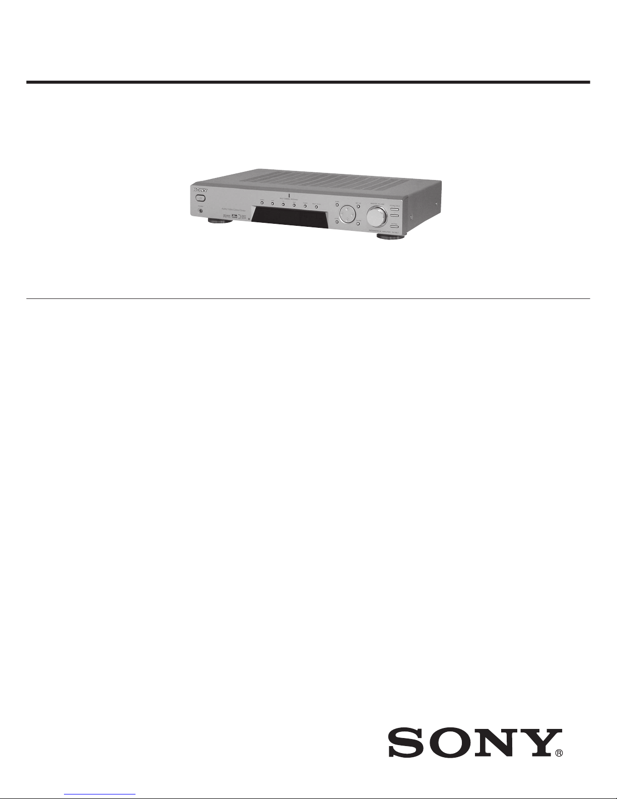
Photo : TA-KSL7
Dolby Laboratories Licensing Corporation.
“DOLBY” the double-D symbol ; “AC-3” and “PRO LOGIC”
are trademarks of Dolby Laboratories Licensing Corporation.
Amplifier section
POWER OUTPUT
Rated Power Output at Stereo mode
(8 ohms 1 kHz, THD 0.3 %)
80 W + 80 W
Reference Power Output
(THD 0.3 %) Front
1)
: 80 W/ch
Center
1)
: 80 W
Surround
1)
: 80 W/ch
1) Depending on the sound field settings and the
source, there may be no sound output.
Frequency response
MICRO SP.: 150 Hz – 20 kHz
0/–3 dB
150 Hz (6 dB/oct)
Low cut Filter ON
NORMAL SP.: 20 Hz – 20 kHz
+/–0.5 dB
Outputs
FRONT L/R, CENTER, SURROUND L/R,
SUB WOOFER Voltage: 2 V
Impedance: 1 kilohms
Video section
Inputs
S-video: Y: 1 Vp-p, 75 ohms
C: 0.286 Vp-p, 75 ohms
Outputs
S-video: Y: 1 Vp-p, 75 ohms
C: 0.286 Vp-p, 75 ohms
FM tuner section
Tuning range 87.5 – 108.0 MHz
Antenna terminals 75 ohms, unbalanced
Intermediate frequency
10.7 MHz
Sensitivity Mono: 18.3 dBf,
2.2 µV/75 ohms
Stereo: 38.3 dBf,
22.5 µV/75 ohms
Usable sensitivity 11.2 dBf, 1 µV/75 ohms
S/N Mono: 76 dB
Stereo: 70 dB
Harmonic distortion at 1 kHz
Mono: 0.3%
Stereo: 0.5%
Separation 45 dB at 1 kHz
Frequency response 30 Hz – 15 kHz
+0.5/–2 dB
Selectivity 60 dB at 400 kHz
Inputs (Analog) Sensitivity: 250 mV
Impedance: 50 kilohms
S/N
2)
: 80 dB
(A, 20 kHz LPF,
250 mV
3)
)
2) INPUT SHORT.
3) Weighted network, input level.
Inputs (Digital)
DVD (Coaxial) Sensitivity: –
Impedance: 75 ohms
S/N: 96 dB
(A, 20 kHz LPF)
TV, AUX (Optical) Sensitivity: –
Impedance: –
S/N: 96 dB
(A, 20 kHz LPF)
Inputs (Analog) Sensitivity: 250 mV
Impedance: 50 kilohms
S/N
2)
: 95 dB
(A, 250 mV
3)
)
2) INPUT SHORT.
3) Weighted network, input level.
Inputs (Digital)
DVD (Coaxial) Sensitivity: –
Impedance: 75 ohms
S/N: 95 dB
(A, 20 kHz LPF)
TV, AUX (Optical) Sensitivity: –
Impedance: –
S/N: 95 dB
(A, 20 kHz LPF)
TA-KSL7 : AEP, UK models
EXCEPT TA-KSL7 : AEP, UK models
EXCEPT TA-KSL7
— Continued on next page —
• STR-KSL7 is the receiver section in HT-SL7.
TA-KSL7 is the amplifier section in HT-SL7A.

2
STR-KSL7/SL7/TA-KSL7
After correcting the original service problem, perform the
following safety checks before releasing the set to the customer:
Check the antenna terminals, metal trim, “metallized” knobs, screws,
and all other exposed metal parts for A C leakag e. Check leakage as
described below.
LEAKAGE
The A C leakage from an y exposed metal part to earth ground and
from all exposed metal parts to any exposed metal part having a
return to chassis, must not exceed 0.5 mA (500 microamperes).
Leakage current can be measured by any one of three methods.
1. A commercial leakage tester, such as the Simpson 229 or RCA
WT -540A. Follo w the manufacturers’ instructions to use these
instruments.
2. A battery-operated AC milliammeter. The Data Precision 245
digital multimeter is suitable for this job.
3. Measuring the voltage drop across a resistor by means of a
VOM or battery-operated AC v oltmeter . The “limit” indication
is 0.75 V, so analog meters must ha ve an accurate lo w-v olta ge
scale. The Simpson 250 and Sanwa SH-63Trd are examples of
a passive VOM that is suitable. Nearly all battery operated
digital multimeters that have a 2V AC range are suitable. (See
Fig. A)
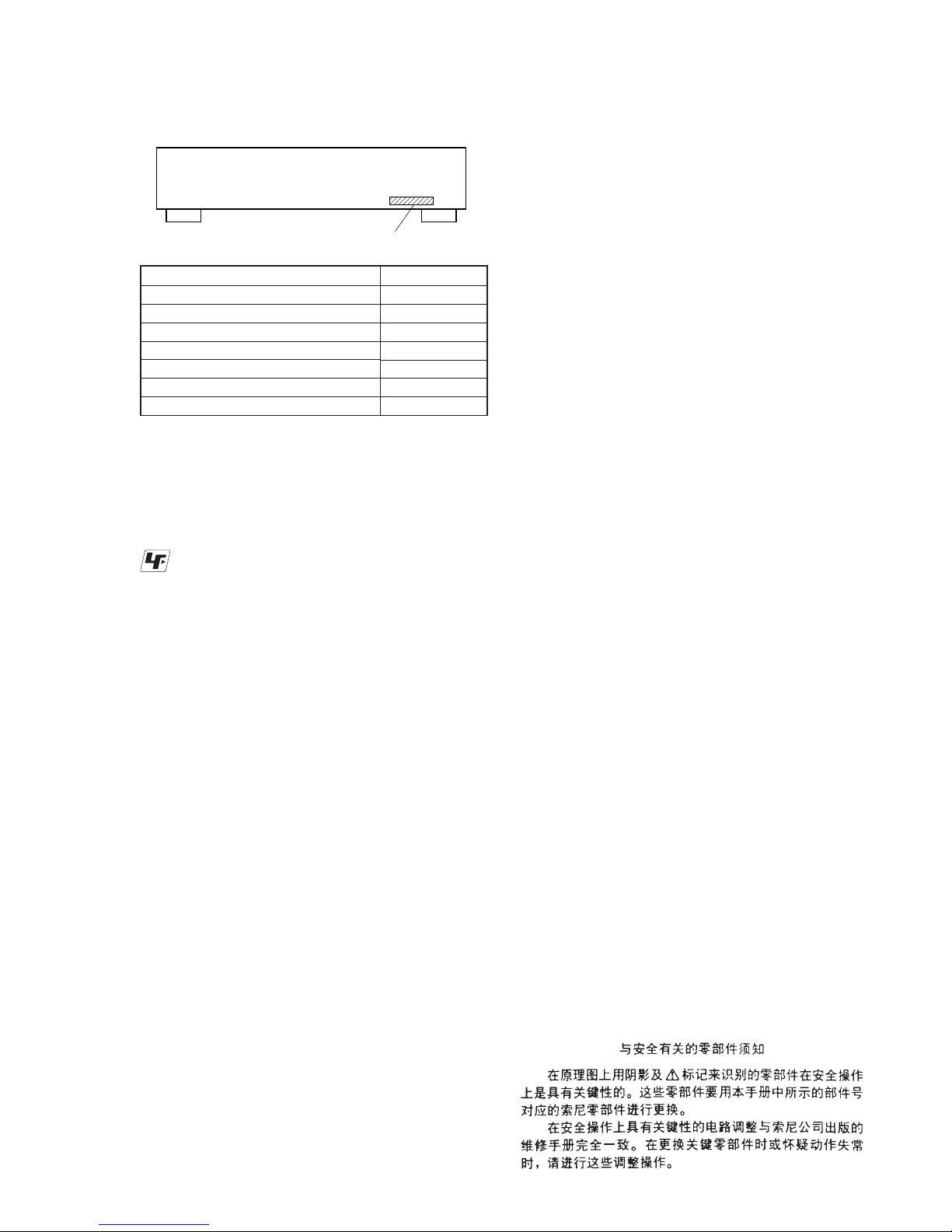
SAFETY CHECK-OUT
To Exposed Metal
Parts on Set
0.15 µF
1.5 kΩ
AC
Voltmeter
(0.75 V)
Earth Ground
Fig. A. Using an AC voltmeter to check AC leakage.
AM tuner section
Tuning range
With 10-kHz tuning scale:
530 – 1710 kHz
With 9-kHz tuning scale:
531 – 1710 kHz
With 10-kHz tuning scale:
530 – 1610 kHz
With 9-kHz tuning scale:
531 – 1602 kHz
530 – 1610 kHz
531 – 1602 kHz
Antenna Loop antenna
Intermediate frequency
450 kHz
Usable sensitivity 50 dB/m (at 1,000 kHz or
999 kHz)
S/N 54 dB (at 50 mV/m)
Harmonic distortion 0.5% (50 mV/m, 400 Hz)
Selectivity At 9 kHz: 35 dB
At 10 kHz: 40 dB
4) You can change the AM tuning scale to 9 kHz
10 kHz. After tuning in any AM station, turn off
the receiver. Hold down the + button and press the
button. All preset stations will be erased when
you change the tuning scale. To reset the scale to
10 kHz (or 9 kHz), repeat the procedure.
General
Power requirements
120 V AC, 60 Hz
110 – 120 V AC,
50/60 Hz
220 – 230 V AC,
50/60 Hz
230 V AC,
50/60 Hz
Power consumption 98 W
Power consumption (during standby mode)
1.7 W
1.9 W
Dimensions (w/h/d) 430 × 83 × 289 mm
including projecting parts
and controls
Mass (Approx.) 3.1 kg
US, Canadian models
E model
Mexican model
Malaysia, Singapore
models
STR-SL7 : US, STR-KSL7, Canadian, Mexican models
STR-SL7 : US, STR-KSL7, Canadian, Mexican models
TA-KSL7 : AEP, UK, Chinese models
STR-KSL7 : E model
STR-KSL7 : Malaysia, Singapore models
STR-KSL7 : Malaysia, Singapore models
STR-SL7 : US model
Supplied accessories
FM wire antenna (1)
AM loop antenna (1)
Remote commander RM-U305S (1)
R6 (size-AA) batteries (2)
Design and specifications are subject to change
without notice.
EXCEPT TA-KSL7
3
STR-KSL7/SL7/TA-KSL7
SAFETY-RELATED COMPONENT WARNING!!
COMPONENTS IDENTIFIED BY MARK 0 OR DOTTED LINE WITH
MARK 0 ON THE SCHEMATIC DIAGRAMS AND IN THE PARTS
LIST ARE CRITICAL TO SAFE OPERATION. REPLACE THESE
COMPONENTS WITH SONY PARTS WHOSE PART NUMBERS
APPEAR AS SHOWN IN THIS MANUAL OR IN SUPPLEMENTS
PUBLISHED BY SONY.
ATTENTION AU COMPOSANT AYANT RAPPORT
À LA SÉCURITÉ!
LES COMPOSANTS IDENTIFÉS PAR UNE MARQUE 0 SUR LES
DIAGRAMMES SCHÉMATIQUES ET LA LISTE DES PIÈCES SONT
CRITIQUES POUR LA SÉCURITÉ DE FONCTIONNEMENT. NE
REMPLACER CES COMPOSANTS QUE PAR DES PIÈSES SONY
DONT LES NUMÉROS SONT DONNÉS DANS CE MANUEL OU
DANS LES SUPPÉMENTS PUBLIÉS PAR SONY.
MODEL IDENTIFICATION
— BACK PANEL —
PARTS No.
4-235-042-1s
4-235-042-2s
4-235-042-3s
4-235-042-4s
4-235-042-5s
4-235-042-7s
4-235-042-9s
MODEL
STR-SL7 :US model
STR-KSL7 :Canadian model
STR-KSL7 :Malaysia, Singapore model
STR-KSL7 :E model
STR-KSL7 :Mexican model
TA-KSL7 :AEP, UK model
TA-KSL7 :Chinese model
1. GENERAL ·········································································· 4
2. TEST MODE ······································································5
3. DIAGRAMS ········································································ 7
3-1. Block Diagrams ····························································· 8
– Main Section – ··························································· 8
– Display/Power Section – ············································ 9
3-2. Printed Wiring Board – Digital Section – ·················· 10
3-3. Schematic Diagram – Digital Section (1/2) – ············ 11
3-4. Schematic Diagram – Digital Section (2/2) – ············ 12
3-5. Printed Wiring Board – Main Section (1/2) – ············ 13
3-6. Printed Wiring Board – Main Section (2/2) – ············ 14
3-7. Schematic Diagram – Main Section (1/3) – ··············· 15
3-8. Schematic Diagram – Main Section (2/3) – ··············· 16
3-9. Schematic Diagram – Main Section (3/3) – ··············· 17
3-10.Printed Wiring Board – Panel Section – ····················· 18
3-11.Schematic Diagram – Panel Section – ·······················19
3-12.Schematic Diagram – Video Section – ······················· 20
3-13.Printed Wiring Board – Video Section – ···················· 21
3-14.IC Block Diagrams ······················································ 22
3-15.IC Pin Function Descriptions ······································ 25
4. EXPLODED VIEWS ······················································29
4-1. Front Panel Section ····················································· 29
4-2. Chassis Section ···························································· 30
5. ELECTRICAL PARTS LIST ·······································31
Parts No.
TABLE OF CONTENTS
Unleaded solder
Boards requiring use of unleaded solder are printed with the leadfree mark (LF) indicating the solder contains no lead.
(Caution: Some printed circuit boards may not come printed with
the lead free mark due to their particular size.)
: LEAD FREE MARK
Unleaded solder has the following characteristics.
• Unleaded solder melts at a temperature about 40°C higher than
ordinary solder.
Ordinary soldering irons can be used but the iron tip has to be
applied to the solder joint for a slightly longer time.
Soldering irons using a temperature regulator should be set to
about 350°C.
Caution: The printed pattern (copper foil) may peel away if the
heated tip is applied for too long, so be careful!
• Strong viscosity
Unleaded solder is more viscous (sticky, less prone to flow) than
ordinary solder so use caution not to let solder bridges occur such
as on IC pins, etc.
• Usable with ordinary solder
It is best to use only unleaded solder but unleaded solder may
also be added to ordinary solder.
Notes on chip component replacement
• Never reuse a disconnected chip component.
• Notice that the minus side of a tantalum capacitor may be damaged
by heat.
4
STR-KSL7/SL7/TA-KSL7
SECTION 1
GENERAL
This section is extracted
from instruction manual.
AUX 6 (18)
Cursor buttons (U/u) qh (14,
22–24)
Display qk (21)
DVD 3 (18)
LEVEL qj (22)
MASTER VOLUME qa (17, 18)
MULTI CH IN 8 (18)
MULTI CHANNEL DECODING
indicator 5
MUTING qd (18)
PHONES jack ql (18)
SET UP q; (14, 24)
SOUND FIELD +/– qs (19, 23)
SURR 9 (23)
TEST TONE qf (17)
TUNER 7 (18)
TV 4 (18)
VIDEO 2 (18)
?/1 (power) 1 (13, 17, 18, 23)
+/– qg (14, 22–24)
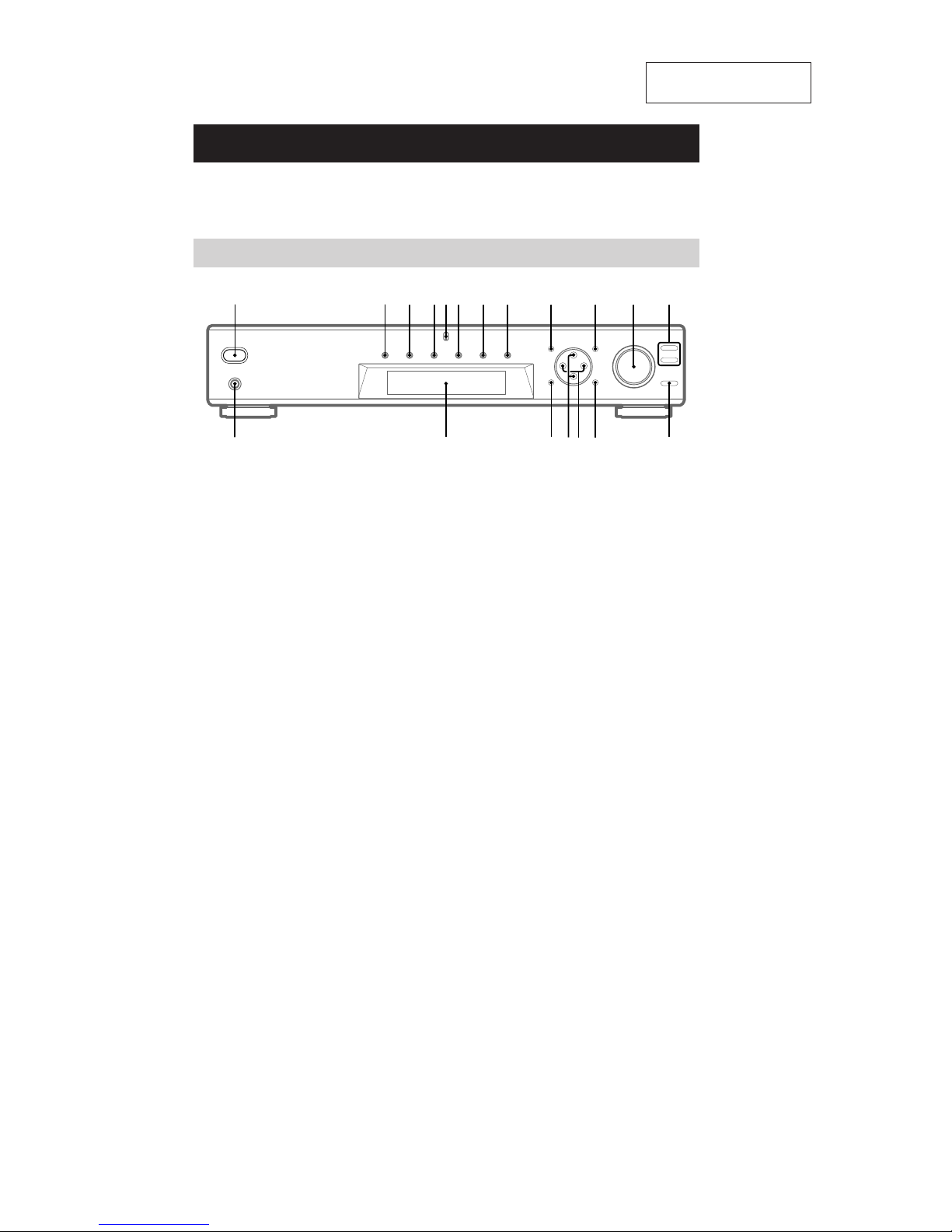
Main unit
1 2 3 456 7
8
9 q; qa qs
ql
qk
qjqfqgqh
qd
Parts Identification
The items are arranged in alphabetical order.
Refer to the pages indicated in parentheses ( ) for details.
5
STR-KSL7/SL7/TA-KSL7
SECTION 2
TEST MODE
FACTORY SET MODE
* All preset contents are reset to the default setting.
* Procedure:
While depressing the SET UP and the SOUND FIELD – buttons
simultaneously, press the power
?/1
button to turn on the main
power. The message FACTORY appears and switch off the set.
While depressing the SET UP and the SOUND FIELD – buttons
simultaneously, press the po wer
?/1
button again. The message
FA CTOR Y appears and the present contents are reset to the def ault
values.
AM CHANNEL STEP 9 kHz/10 kHz
SELECTION MODE
* Either the 9 kHz step or 10 kHz step can be selected for the AM
channel step.
* Procedure:
Set the FUNCTION to AM. Turn off the main power.
While depressing the i cursor button, press the power
?/1
button to turn on the main power . Either the message 9 k STEP or
10 k STEP appears. Select the desired step.
* For US/Canadian/E model only
MICRO/NORMAL SPEAKER SELECTION MODE
* Either the micro speaker mode or normal speaker mode can be
selected.
* Procedure
Press the
?/1
button while pressing the + cursor button to turn
on the power. Either the message MICRO SP. or NORM. SP.
appears. Select the derired mode.
SOUND FIELD CLEAR MODE
* The preset sound field is cleared when this mode is activated.
Use this mode before returning the product to clients upon
completion of repair.
* Procedure:
While depressing the SOUND FIELD + button, press the power
?/1
button to turn on the main power. The message
S. F. CLR appears and initialization is performed.
DEMONSTRATION MODE
* Demonstration is performed.
* Procedure :
While depressing the SET UP button, press the power
?/1
button. The message appears and demonstration is performed.
* To finish DEMONSTRATION MODE, press the power
?/1
button while the introduction message appears in the display.
FLUORESCENT INDICATOR TUBE TEST MODE
* All fluorescent segments are tested. When this test is activated,
all segments turn on at the same time, then each segment turns on
one after another.
* Procedure:
While depressing the SET UP and the SOUND FIELD + buttons
simultaneously, press the po wer
?/1
button to turn on the main
power.
1. All segments turn on.
DVD , TV , MULTI CH IN and SURR LED turn on.
2. Press the VIDEO button, confirm display
AUX , TUNER and LEVEL LED turn on.
3. Press the VIDEO button, confirm display
MUL TI CHANNEL DECODING(blue), VIDEO and SET UP
LED turn on.
4. Press the VIDEO button, All segments turn off.
5. Every pressing of the VIDEO button turns on each segment and
LED one after another in the same order.
(Not only the VIDEO button, b ut also the other b uttons such as
DVD , TV , AUX , TUNER can be used.)
KEY CHECK MODE
* Button check
* Procedure:
While depressing the MUTING and the ENTER buttons
simultaneously, press the po wer
?/1
button to turn on the main
power.
REST 17 appears.
Every pressing of any button other than ?/1 counts down the
buttons. The buttons which are already counted once are not
counted again. When all buttons are pressed REST 00 appears.
SW
LSLCR
SSR
SLEEP
SP.OFF
( ( ( L F E ) ) )
DIGITAL
OPT COAX MULTI CH IN
PRO LOGIC DTS MPEGSTEREO MONORDS MEMORY
MUTINGINFONEWSTAEQD.RANGE
D
D
dB
kHz
mft.
MHz
SW
LR
S
SLEEP
L F E
COAX
PRO LOGIC MPEGSTEREO RDS
MUTINGINFOTAD.RANGE
D
D
k
m
MHz
SL
C
SR
SP.OFF
( ( ( ) ) )
DIGITAL
OPT MULTI CH IN
DTS MONO MEMORY
NEWSEQ
dB
Hz
ft.

6
STR-KSL7/SL7/TA-KSL7
AUTOBETICAL MODE (TA-KSL7: AEP, UK)
* This mode is installed in the Europe models only . When this mode
is used, the receiver scans the broadcasts that can be received by
tuner, and sets up the broadcasts. Be sure to start scanning after
connecting the antenna.
Procedure:
Check that the antenna is connected. Press the ?/1 button while
pressing the ENTER button to turn on the power. The message
appears and scanning starts by tuner.
SOFTWARE VERSION DISPLAY MODE
* The software version is displayed.
* Procedure:
While depressing the SOUND FIELD – and the i cursor buttons
simultaneously, press the po wer
?/1
button to turn on the main
power . The model name, destination and the software version are
displayed.
77
STR-KSL7/SL7/TA-KSL7
SECTION 3
DIAGRAMS
For schematic diagrams.
Note:
• All capacitors are in µF unless otherwise noted. p : pF. 50
WV or less are not indicated except for electrolytics and
tantalums.
• All resistors are in Ω and
1
/
4
W or less unless otherwise
specified.
• % : indicates tolerance.
•f: internal component.
• C : panel designation.
• A : B+ Line.
• B : B– Line.
• Voltages and waveforms are dc with respect to ground
under no-signal (detuned) conditions.
No mark : FM
• Voltages are taken with a VOM (Input impedance 10 MΩ).
Voltage variations may be noted due to normal production tolerances.
• Waveforms are taken with a oscilloscope.
• Circled numbers refer to waveforms.
• Signal path.
F : ANALOG
J : DIGITAL
c : DVD
• Abbreviation
CND : Canadian model
MY : Malaysia model
SP : Singapore model
CH : Chinese model
MX : Mexican model
THIS NOTE IS COMMON FOR PRINTED WIRING BOARDS AND SCHEMATIC DIAGRAMS.
(In addition to this necessary note is printed in each block.)
Note:
The components identified by
mark 0 or dotted line with mark
0 are critical for safety.
Replace only with part number
specified.
Note:
Les composants identifiés par
une marque 0 sont critiques
pour la sécurité.
Ne les remplacer que par une
pièce portant le numéro spécifié.
C
B
These are omitted.
E
Q
B
These are omitted.
CE
For printed wiring boards.
Note:
• X : parts extracted from the component side.
•a: Through hole.
•f: internal component.
• : Pattern from the side which enables seeing.
Caution:
Pattern face side: Parts on the pattern face side seen from
(Side A) the pattern face are indicated.
Parts face side: Parts on the parts face side seen from
(Side B) the parts face are indicated.
• CIRCUIT BOARDS LOCATION
• WAVEFORMS
– DIGITAL BOARD – – MAIN BOARD – – DISPLAY BOARD –
1
IC506 5
2
IC701 9
3
IC101 id
6Vp-p
81ns
20ns/div 2V/div
6.3Vp-p
81ns
20ns/div 2V/div
5.8Vp-p
62ns
20ns/div 2V/div
5Vp-p
1.3
µ
s
400ns/div 2V/div
4
IC306 4
5
IC309 wf
7.8Vp-p
20.3ns
10ns/div 2V/div
25.4Vp-p
9.8
µ
s
4 µs/div 10V/div
6
Q153 collector
HEADPHONE board
POWER SW board
MAIN board
DIGITAL board
S VIDEO board
DISPLAY board
• MAIN board consists of multiple layers.
However, only the sides (layers) A and B are shown.
88
STR-KSL7/SL7/TA-KSL7
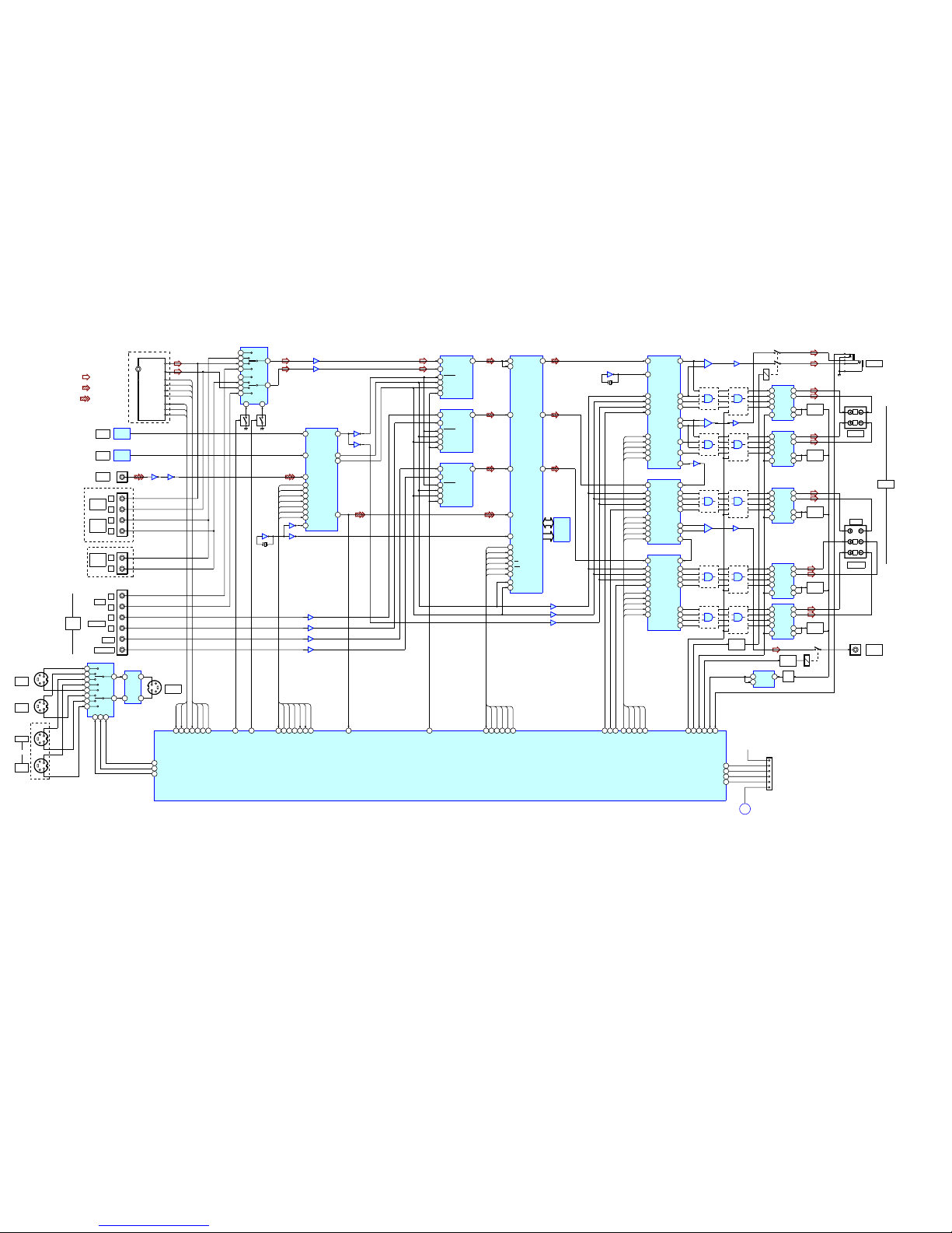
3-1. BLOCK DIAGRAMS
– MAIN SECTION –
• Signal Path
: ANALOG
: DIGITAL
: DVD
T DATA
T DO
T CLK
T CE
STEREO
TUNED
MUTING
DATA
DO
CLK
CE
STEREO
TUNED
MUTING
R OUT
L OUT
MULTI
CH
INPUT
J207
66
TUNED
SW2
76
SW1
75
VIDEO INH
74
65
T MUTE
67
STEREO
62
TUNER DO
60
TUNER DATA
61
TUNER CLK
59
TUNER CE
78
SW A79SW B
SYSTEM CONTROL
IC101(1/2)
IC502
DIGITAL AUDIO
I/F RECEIVER
IC504
DIN0
3
DIN1
4
DO
35
DI
36
CLK
38
CE
37
ERROR
34
XSTATE
17
XMODE
48
XIN
22
DIR DO
DIR DI
DIR CLK
DIR CE
ERROR
XSTATE
XMODE
13CK OUT
14
BCK
15
LRCK
16DATAO
17
IC506
X501
12.288MHz
AUDIO DSP
IC701
SDIA1
85
SO
67
SI
68
SCK
69
CS
66
CSB
65
IC
62
XI
8
DSP SO
47
SDOB0
46
SDOB1
45SDOB2
SDIB0
5
DSP SI
DSP CLK
DSP CS
DSP CSB
DSP IC
35
IC506
IC703
SRAM
IC309
SCDT
38
SCSHIFT
37
NSPMUTE
39
PGMUTE
40
INIT
41
24
OUTL1+
XFSOIN
28
21
OUTL1-
15
OUTL2+
18
OUTL2-
DATA
43
90 89 87 88 91 92 85 93
DIR DO
DIR DI
DIR CLK
DIR CE
ERROR
XSTATE
XMODE
DIR DATA
24
DSP SO
DIR DO
DIR DI
DIR CLK
DIR CE
ERROR
XSTATE
XMODE
22
DSP SI
21
DSP CLK
25
DSP CS
99
DSP CSB
100
DSP IC
10
S DATA
DSP SO
DSP SI
DSP CLK
DSP CS
DSP CSB
DSP IC
9
S SHIFT
13
NSP MUTE
14
PG MUTE
15
RST
19FLASH DATA OUT
20FLASH DATA IN
49MD0
51MD2
VDD
FLASH1
FLASH2
MD0
MD2
RESET
+5V
(STBY)
CNP104
A
FM
AM
TUNER UNIT
EXCEPT TA-KSL7
IC501
J301
3562
IC503 IC503
TUNER
IN
VIDEO
AUDIO
IN
VIDEO
AUDIO
IN
R
L
J205
R
L
TA-KSL7
MODEL
12
13
14
15
11
10
IC203
1
3
5
2
4
9
A
B
31
Q203
Q205
Q202
Q204
DIN2
5
62
IC506
35
IC505
17
IC505
A/D CONV.
IC606
L IN
1
15
D OUT
R IN
5
SYSCLK
16
BCK
14
LRCK
13
RSTB
6
57
IC603
A/D CONV.
IC604
L IN
1
15D OUT
R IN
5
SYSCLK
16
BCK
14
LRCK
13
RSTB
6
A/D CONV.
IC605
L IN
1
15
D OUT
R IN
5
SYSCLK
16
BCK
14
LRCK
13
RSTB
6
31
IC602
57
IC602
31
IC601
57
IC601
24
IC306
X306
49.152MHz
SDIAO
84
SDBCK0
83
SDWCK0
82
5
RST AD
17
3
5
62
IC322
SDIB2
7
SDIB1
6
BCK
44
LRCK
45
XFSI
64
SCLATCH
36
SCDT
SCSHIFT
NSPMUTE
PGMUTE
INIT
5
6
7
IC801
56
IC802
PULSE SHAPER
PULSE SHAPER
PULSE SHAPER
PULSE SHAPER
PULSE SHAPER
IC307
GATE
GATE
GATE
GATE
GATE
IC308
4
3
9
8
5
RY801
RY201
L
R
FRONT
SPEAKERS
PHONES
SURROUND
CENTER
TM802
TM801
SUB
WOOFER
J204
J101
15
11
16
12
PROTECT
Q401
POWER
DRIVER
POWER
DRIVER
POWER
DRIVER
POWER
DRIVER
POWER
DRIVER
IC301
10
OUTR1+
3
2
1
IC801
31
IC802
1
OUTR2+
7
OUTR1-
4
OUTR2-
IC310
IC311
4
3
9
8
5
15
11
16
12
PROTECT
Q402
IC302
24
IC324
77
XFSO OUT
IC315
SCDT
38
SCSHIFT
37
NSPMUTE
39
PGMUTE
40
INIT
41
28XFSO IN
21
OUTL1-
15
OUTL2+
18
OUTL2-
DATA
43
BCK
44
LRCK
45
XFSI
64
SCLATCH
36
SCDT
SCSHIFT
NSPMUTE
PGMUTE
INIT
IC312
IC313
4
3
9
8
5
15
11
16
12
PROTECT
Q403
IC303
10OUTR1+
5
6
7
IC314
31
IC314
1OUTR2+
24
OUTL1+
77
XFSO OUT
IC318
SCDT
38
SCSHIFT
37
NSPMUTE
39
PGMUTE
40
INIT
41
28
XFSO IN
21
OUTL1-
15
OUTL2+
18
OUTL2-
DATA
43
BCK
44
LRCK
45
XFSI
64
SCLATCH
36
SCDT
SCSHIFT
NSPMUTE
PG MUTE
INIT
IC316
IC317
4
3
9
8
5
15
11
16
12
PROTECT
Q404
IC304
24
OUTL1+
7
OUTR1-
1
OUTR2+
4
OUTR2-
IC319 IC320
4
3
9
8
5
15
11
16
12
PROTECT
Q405
IC305
10
OUTR1+
RELAY SW
Q201
BUFF
Q406
3D0
Q0
2
LE
11
LATCH
IC321
TUNED
MUTING
STEREO
T DO
T DATA
T CLK
T CE
8
AMP CE17AMP CE26AMP CE3
SC DT
SC SHIFT
NSP MUTE
PG MUTE
INIT
12EN70
HP RY
48
DIAG
69
SP RY
53
I LIMT
55
HP SW
RELAY SW
Q801
FLASH
PROGRAMING
VIDEO
IN
DVD
IN
TV IN
AUX
IN
J202
J203(1/2)
C
Y
VIDEO
AMP
IC202
5
1
8
4
J203(2/2)
MONITOR
OUT
12
13
14
15
11
10
IC201
1
3
5
2
4
9
A
B
C
Y
C
Y
C
Y
J201
6
EN
C
Y
J205
R
L
R
L
R
L
FRONT
SURROUND
SUB WOOFER
CENTER
EXCEPT
TA-KSL7
OPTICAL
RECEIVER
OPTICAL
RECEIVER
STREAM PROCESSOR
STREAM PROCESSOR
STREAM PROCESSOR
DVD
COAXIAL
AUX
OPTICAL
TV
OPTICAL
L
R
99
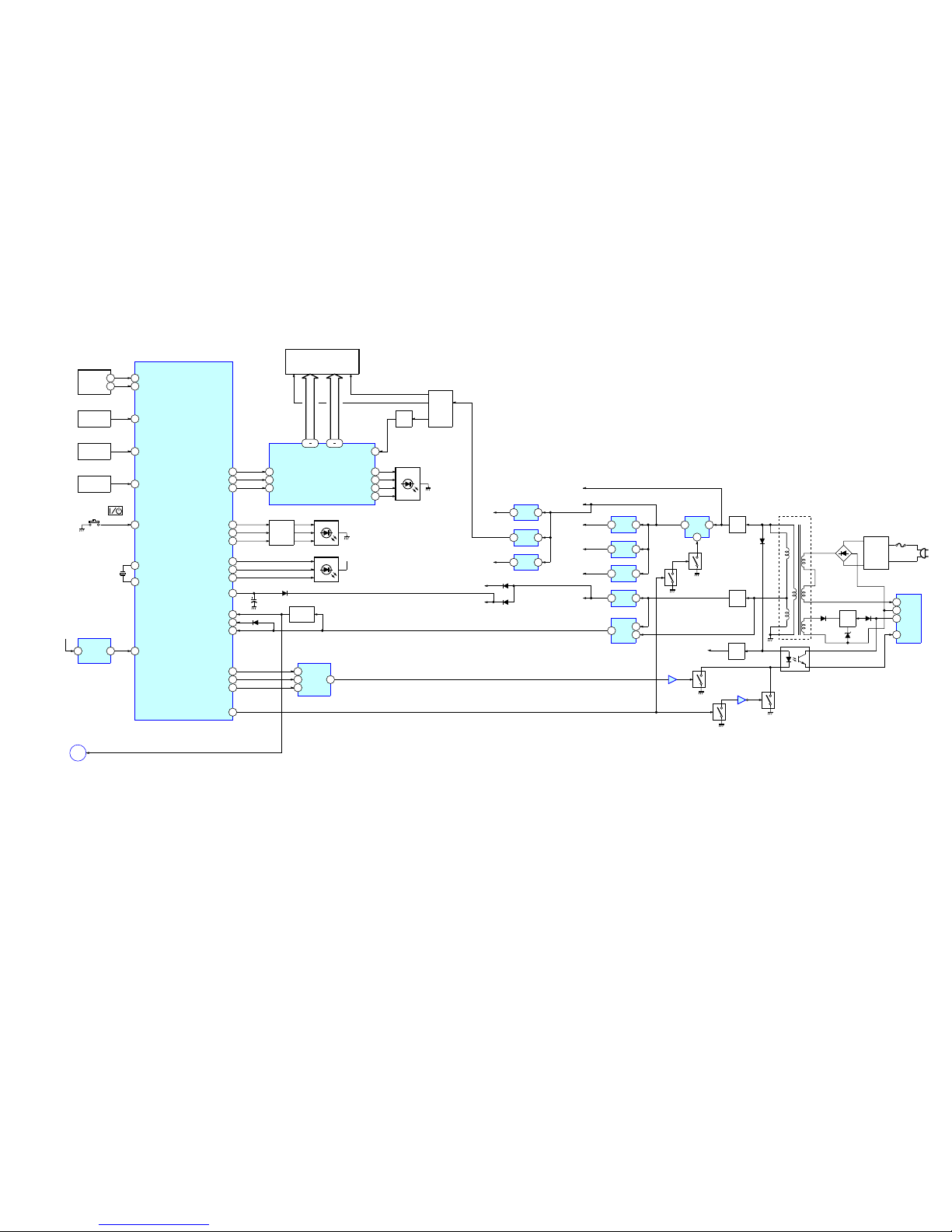
STR-KSL7/SL7/TA-KSL7
– DISPLAY/POWER SECTION –
RESET SW
Q101
RECT
D159-162
77
RESET
47STOP
REMOTE
CONTROL
RECEIVER
1
3
IC151
X101
16MHz
FLUORESCENT
INDICATOR TUBE
FL101
14 29
SEG1-16
42 31
GRID1-12
4
VIDEO LED
3
DVD LED
2
TV LED
1
AUX LED
FL/LED DRIVE
IC152
D151-154
FUNCTION
KEY
S107-112
S114,117
52HSTX
D104
D101
A
RESET
SYSTEM CONTROL
IC101(2/2)
T901
AC
IN
POWER TRANS
LF901,902
LINE
FILTER
D902
F901
REG
Q903
REG
Q904
D
3
S
2
VCC
4
FB/OCP
1
IC901
SWITCHING REG
PC901
RECT
D911
RECT
D909
Q901
Q902
+5.6V
REG
1
3
IC905
+12V
REG
1
2
IC903
5
Q906
Q908
RESET
8
5
6
IC910
+5V
REG
1
3
IC102
+9V
16
FL DATA
KEY INPUT1
38
RV101
VOL
ENCODER
1
3
VOL UP
43
VOL DOWN
44
FUNCTION
KEY
S113,115,116
KEY INPUT2
39
FUNCTION
KEY
S101-106
KEY INPUT3
40
POWER SW56
POWER
ON/OFF
S118
31
LED MCD
17
FL CLK
18
FL LATCH
DC/DC
CONV.
Q152,153
T101
CLK8
DIN
7
STB
9
30
VEE
LED
DRIVE
Q151,154,155
33
LED 5.1
32
TUNER
D121,155,156
3MENU
2TUNER
4SET UP
27C
D157,163,164
+5V
+5V
(STBY)
D906 D905
D903
IC907
Q915
24
D910
+9V
REG
1
3
IC909
+5V
+5V
REG
1
3
IC908
+3,3V
+3.3V
REG
1
3
IC906
+5.6V
+5V
+7V
+7V
REG
1
3
IC104
+12V
+40V
+5V
REG
1
3
IC706
+5V
D1403
D103
C103
0.22F
µCOM VDD
+5V(STBY)
Q905
21
IC902
TO IC902
1
A01
DATA
6
CLK
7
CE
8
96
DATA
97
CLK
98
CE
V CONT
IC103
28
POWER ON/OFF
XO
82
XI
83
SIRCS57
1010
STR-KSL7/SL7/TA-KSL7
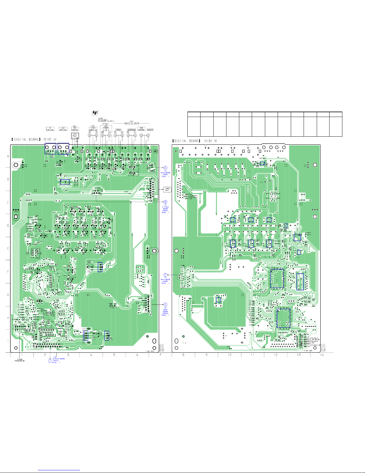
3-2. PRINTED WIRING BOARD – DIGITAL SECTION –
• : Uses unleaded solder. • See page 7 for Circuit Boards Location.
IC203
IC102
IC104
IC701
IC506
IC504
IC505
IC606IC605
IC604
IC603
IC602
IC601
IC503
IC703
IC101
IC103
IC706
IC502 IC501
18
13
14
21
13
C501
EXCEPT TA-KSL7
EXCEPT TA-KSL7
EXCEPT TA-KSL7
Ref. No. Location
• Semiconductor Location
Ref. No. Location Ref. No. Location
D101 H-3
D102 I-2
D103 H-3
D104 I-2
D1403 I-3
IC101 H-12
IC102 I-4
IC103 G-9
IC104 I-5
IC203 B-3
IC501 A-3
IC502 A-2
IC503 A-11
IC504 D-13
IC505 D-12
IC506 E-13
IC601 D-10
Ref. No. Location Ref. No. Location
IC602 D-11
IC603 D-12
IC604 E-10
IC605 E-11
IC606 E-12
IC701 F-12
IC703 F-13
IC706 F-4
Q101 I-2
Q202 C-12
Q203 C-12
Q204 C-12
Q205 C-12
Ref. No. Location
1111
STR-KSL7/SL7/TA-KSL7
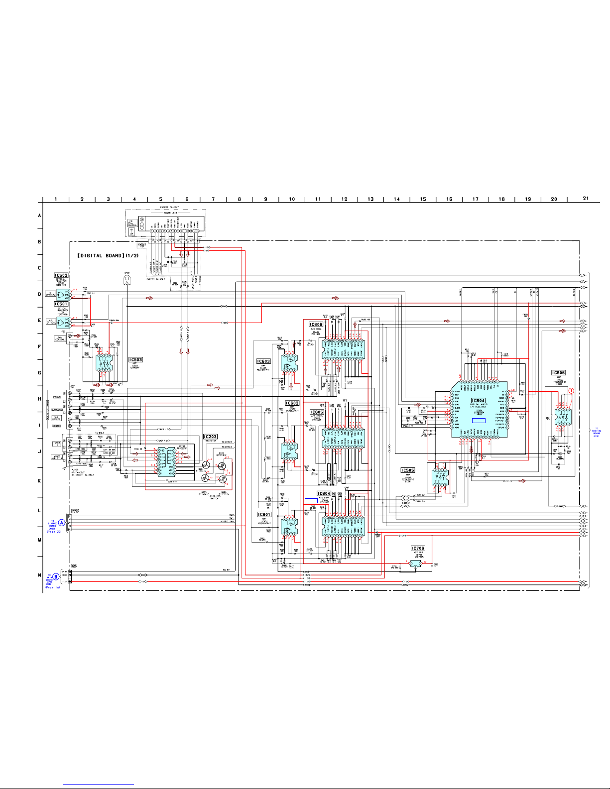
3-3. SCHEMATIC DIAGRAM – DIGITAL SECTION (1/2) –
• See page 7 for Wavefoms. • See page 22, 23 for IC Block Diagrams.
IC B/D
IC B/D
1212
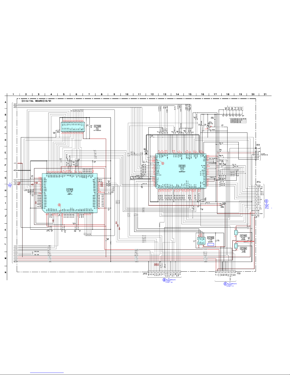
STR-KSL7/SL7/TA-KSL7
3-4. SCHEMATIC DIAGRAM – DIGITAL SECTION (2/2) –
• See page 7 for Wavefoms. • See page 22 for IC Block Diagrams. • See page 25, 27 for IC Pin Function Description.
IC B/D
19
1313
STR-KSL7/SL7/TA-KSL7
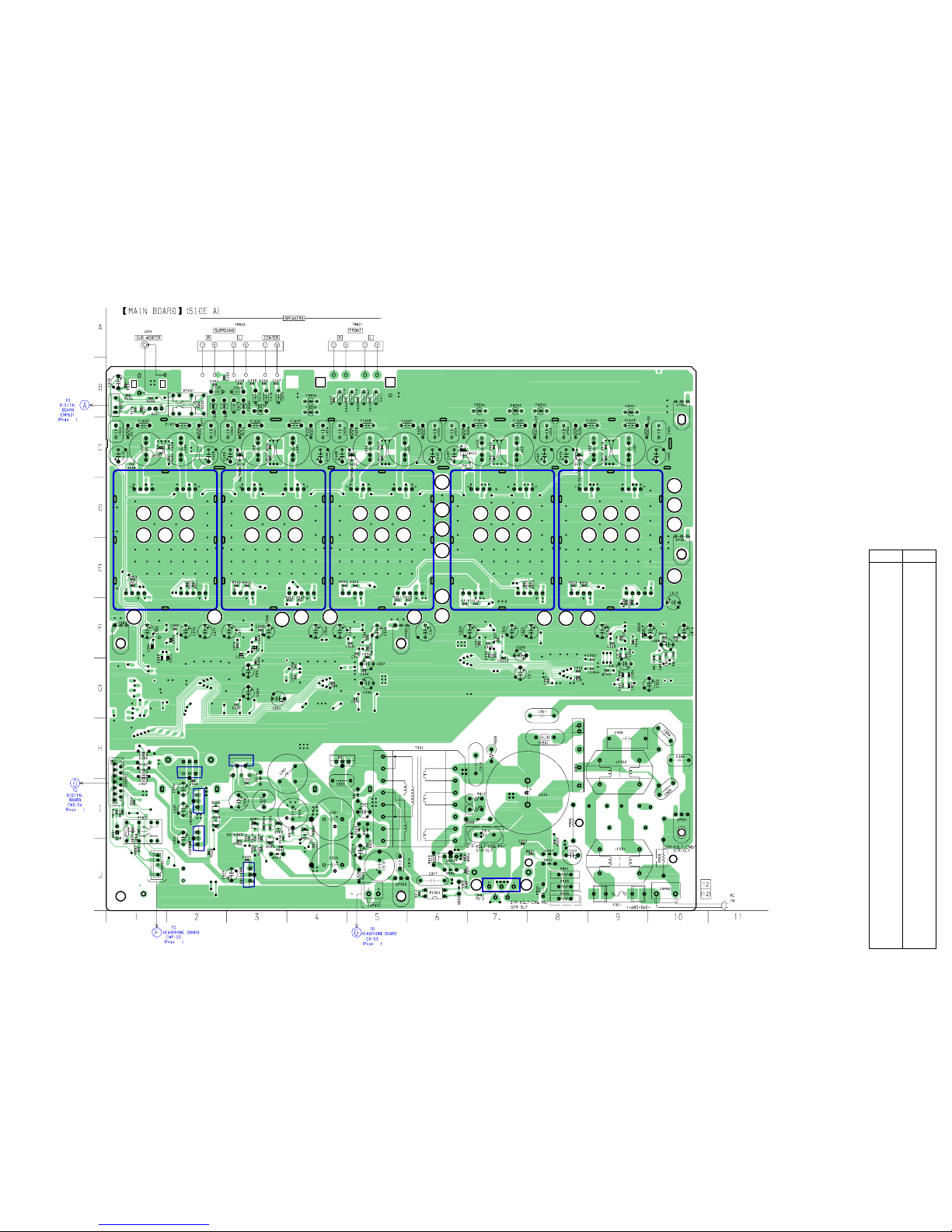
3-5. PRINTED WIRING BOARD – MAIN SECTION (1/2) –
• See page 7 for Circuit Boards Location.
IC305 IC304 IC303 IC302 IC301
IC901
IC905
IC906
IC909
IC908
IC903
18
10
18
10
Ref. No. Location
D203 B-2
D801 I-1
D901 J-8
D902 J-8
D903 J-6
D904 J-6
D905 J-6
D906 J-6
D907 J-8
D908 I-7
D909 I-5
D910 I-5
D911 H-4
D913 J-3
D914 I-3
D915 J-3
D916 I-4
D917 I-5
D918 I-3
IC301 D-9
IC302 D-7
IC303 D-5
IC304 D-3
IC305 D-2
IC901 J-7
IC903 H-3
IC905 J-3
IC906 J-2
IC908 H-2
IC909 I-2
Q201 B-1
Q401 C-8
Q402 C-6
Q403 C-5
Q404 C-3
Q405 C-1
Q801 I-1
Q901 I-3
Q902 I-3
Q903 J-6
Q904 I-4
Q905 J-3
Q906 I-2
Q908 I-2
• Semiconductor
Location
 Loading...