

Sony STR-S5L Service Manual
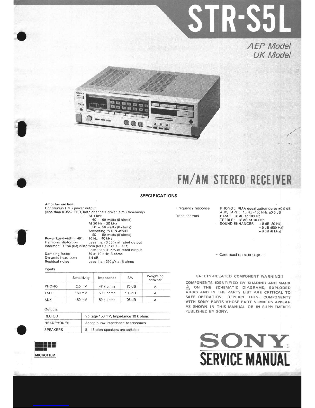
rM/AM
AEP
Model
UK
Model
STEREO
RTGE
I[|ER
SPECIFICATIONS
Amplitier
section
Continuous
RMS
power
output
(less
than 0.05%
THD,
both channels driven simultaneously)
At 1 kHz
60
+ 60 watts
(8
ohms)
At 20
Hz
,20
k{z
50 + 50 watts
(8
ohms)
According to
DIN
45500
50 + 50 watts
(8
ohms)
Power
bandwidth
(lHF)
10 Hz 40 kHz
Harmonic distortion Less than
0.0596 at
rated
output
Intermodulation
(lM)
distortion
(60
Hz:7 kHz = 4: 1)
Less than 0.05% at
rated
outout
Damping
factor
50 at 10 kHz, 8 ohms
Dynamic
headroom 1.4
dB
Residual
noise
Less than
250
fV
at I ohms
I nouts
lmpedance
47 k ohms
76 dB
Frequency response
Tone
controls
PHONO : RIAA
equalization
curve r0.5
dB
AUX,
TAPE :
.10
Hz
-100
kHz
+0.5
dB
BASS :
+8
dB at
.100
Hz
TREBLE
:
+8
dB at 10 kHz
SOUND ENHANCER :
+8 dB
(80
Hz)
+ 6 dB
(800
Hz)
+
I dB
(8
kHz)
Accepts low impedance headphones
-
Continued on next
page
-
SAFETY.BELATED
COMPONENT WARNING!
!
COMPONENTS IDENTIFIED
BY
SHADING AND
MARK
A
oN
THE
ScHEMATIc DIAGRAMS,
EXPLoDED
VIEWS AND IN
THE PARTS
LIST ARE
CRITICAL TO
SAFE OPERATION. REPLACË
THESE
COMPONENTS
WITH
SONY PARTS
WHOSE PART
NUMBERS
APPEAR
AS SHOWN IN
THIS
MANUAL
OR
IN
SUPPLEMENTS
PUBLISHED
BY SONY.
SOhTY
50 k ohms 105 dB
50 k ohms
105
dB
Outputs
REC OUT
HEADPHONES
2-5 mV
SPEAKERS
SERVICE
MANUAL
FM
tunor
seclion
Tuning range
Antenna
terminals
Intermediate
f requency
Sensitivily
Usable sensilivity
Signal-to-noise
ratio
Harmonic
distortion
Separation
Frequency
response
Selectivity
Capture
ratio
AM suppression retio
lmage response ratio
lF response
ratio
Spurious
response ratio
FIF intermodulation
Auto tuning level
87.5
-
108.0 MHz
300 ohms balanced, 75
ohms
unbalanced
10.7 MHz
at
46
dB
quieting
17.3 dBf, 4
fV
(mono)
38.3
dBt,
45
fV
(stereo)
10.3
dBf
,
1 .8
riv
(lH
F)
9.3
dBf , 1.6
gV
(S/N
26 dB)
75
dB
(mono),
70
dB
(stereo)
at 1 kHz
0.15%
(mono),
0.3%
(stereo)
45 dB at 1 kHz
40Hz-12.5kxz
1$5oe
30Hz-15kHz
19idB
55
dB
(300
kHz)
-
60 dB
(400
kHz)
r  da
54 dB
80
dB
100 dB
80
dB
60 dB
19.2 dBf
(at
(at
Selectivity
General
System
Power requirements
Power
consumption
AC outlets
Dimensions
Weight
I
Superheterodyne
FM/AM luner,
pure-complementary
sEPP
AEP model:
22O V ac,50/60
Hz
UK model:
24OV ac.50/60
Hz
AEP model:
120 watts
UK model: 32O
watts
2 switched
total 100 W
Approx.
430 x 130 x 330 mm
(w/h/d)
(17
x
5r/r x 13 inches)
Including
proiecting parts
and
controls
Approx.
9.3 kg
(20
lb I oz),
net
Approx.
11.5
kg
(25
lb 6 oz) in shipping
carton
AM tunor soction
MW
LW
unrng
range
522kHz- 1602
kHz 150 kHz
-350
kHz
Antenna
built-in antenna
provided
provided
external antenna
terminal
provided provided
Intermediate
frequency
450 kHz 450 kHz
Usable sensitivity
built-in antenna
50 dB/m
(1,000
kHz) 60 dB/m
(230
kHz)
external antenna
100rrV
(1,000
kHz)
''l00rrV
(230
kHz)
Signal-to-noise
ratio
(at
50 mv/m)
52 dB
52 dB
Harmonic
distortion
(at
50
mV/m, 400 Hz)
0.3%
03%
35 dB
(9
kHz)
35 dB
(9
kHz)
-2-
Generally, the insulation
resistance of
the
oxide
layer in MOS IC structures
is
very
high, and the oxide
layer
is very thin. Because
of
this,
it
is
possible
that
the static
voltages
usually
present
on clothes and
the
human body
will be
enough
to
generate
a
potential
difference across
the insulator,
high enough
to cause
a breakdown
of the insulating
layer.
The
following
precautions
should be taken while
handling these ICs.
(Particular
care should
be taken under conditions
of
low
humidity.)
Precautions
in Replacing
MOS
lCs
l.
Store
new ICs by
inserting them into a urethane-
polyester
cushion
(which
is
somewhat
conduc-
tive),
or wrapping
it in
aluminum
foil,
so that
all the
pins
are at the same
potential.
(The
ICs
should
be stored in that manner until
mounted
on the circuit board.)
Fig. A
partially
conductive
unrethane-polyester
cushion
Fig.
B
aluminum
foil
Handling Precautions for MOS
lCs
soldered
Fis.
D
Fis.
E
Fis. F
-3-
Equalize any
potential
difference between
the
clothes, the tools
in use, the work bench,
the
set being
worked on, and the
packaged
IC by
touching them all in succession
with the hands
or a conductive
wire or tool.
The
following
are
effective methods
for handl-
ing ICs
thai
remove
the
potential
difference
across
the oxide layer.
o
Use
a
paper
clip
modified by soldering
in a
wire braid
insert.
J.
4.
2.
Check
the soldering
iron for
possible power-line
leakage current.
Make sure that there is
no
leakage
path
by connecting
an ohmmeter to the
tip
of the soldering iron and the
plug
as shown
in Fig.
C.
If there is a leakage
path,
use some
other
soldering
iron.
VOM
(9x
1O.0OO range)
Make sure
that there
is
no solder on
the inside.
cltp
soldered
partially
conductive
urethane-polyester
cushion
or
aluminum
foil
Make
sure that
all the
pins
are in
contact
with the wire braid
hll
the
pins
will then be
at the same
potential.).
wire braid
wire braid

o
Take a short
length
of fine bare
wire
and
wind it
around
the IC so that
it
shorts
all
the
pins
of the
IC, while
it is still in the urethane-
polyester
cushion
or
aluminum foil.
This
ensures
that
all the
pins
are
at the same
potential.
fine
bare wire
(stripped
solid
hookup
wtre.
etc.
)
Precaution
while Checking C-MOS
lCs
The
C-MOS
ICs
(Complementary
MOS) are MOS
ICs
that have
their
output sections
made
up of
N-channel and
P-channel
push-pull
stages
to increase
their speed
of
operation. If
the output terminal of
these ICs comes into contact
with
B+
or
B-
voltage,
then the FET which is
ON
at that time
will
either
become shorted or open.
This
is
valid for
all the output sections that are
connected together by
the interconnections.
Even
the circuits that are
physically
separated
(and
not on
the
same board) can be destroyed simultaneously.
Example:
If this
line is
grounded,
or touches
B+ or B- bus.
.
. , the
output stage
of
this lC will be destroyed.
Fis.
I
I
partially
conductive
u rethane-polyester
cushion or aluminum
foil
Fis.
G
o
When
it is necessary to handle
the
IC
with
the
fingers, do not
touch
any
pin,
and hold
the IC at the
ends of
its
plastic-package
case
as shown
in Fie.
H.
Fis.
H
5. Method
of Mounting
Insert the IC
while holding it with the modified
clip, and solder
all the
pins
with the
clip
still
shorting the
pins. (Similarly,
solder
all the
pins
while
the bare shorting
wire is
still
wound
around them.).
Re'move the clip
or the
bare
shorting
wire
only
after
all the
pins
have been
soldered.
-4-
I
I
STR-S5
SECTION
1
OUTLINE
1-1.
CIRCUIT
DESCRIPTION
ISOUND
ENHANCERI
Figure
A
shows
an
amplifier
from
the
operation
amp.
Its
gain
is
determined
by
NF
resistors (Rl,
R2)
and
the
gain
of
the
operation
amp.
Therefore,
if
frequency
response
is
given
to Rl
and
R2,
the
amp
response
can be
freely
formed.
The
sound
enhancer
circuit
of
this
model
makes
3 kinds
of responses
by
inserting
a resonance
circuit
parallel
to
R2
by
a
switch.
Figure
B
shows
the
resonance
circuit
diagram.
The
section
within
the dotted
line
performs
the
same
task
as
a coil
and,
with
C609,
forms
the
series
reso_
nance
circuit.
Following
is the
explanation
of
the
section
of
the
circuit
within
the dotted
line.
In
Figure
C,
by
raising
the
voltage
at
(S,
charg_
ing
current
i2
flows
to
C2 and
i3
also
flow..
When
i3
flows,
the
potential
at@rises,
so the
potential
at
@
is also
pushed
up
by
this.
At this
time
the
current
i1
flowing
from
the
power
applied
to
@
is
very
small,
and
i2
is
supplied
almost
totally
as
a iesult
of
the
rise
in voltage
at@.
However,
the
charging
current
i2 decreases
as
time
elapses.
Consequently,
since
potentid
at
@
aho
drops,
i1 becomes
ia
and
increases
as
time
elapses.
By
lowering
the
potential
at
@,
the directions
of
current
and voltage
reverse
and
thus
operation
also
reverses.
Therefore,
by
applying
ac
to
point
@
in tH,
circuit,
the
phase
of i1
lags
the
voltage
by
90o.
This
is because
this
circuit
performs
the
same
job
as
a coil.
Q
is determined
by
the
hfe,
etc.,
of R2,
R3,
R4,
Ql.
This circuit
is
called
active
filter,
and
is often
used
in
graphic
equalizers.
Fis.
C
Fig.
A
L___
Fig.
B
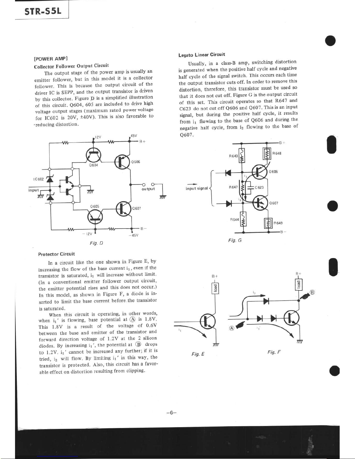
STR.55L
TPOWER
AMP]
Collector
Follower
Output
Circuit
The
output
stage
of
the
power
amp
is
usually
an
emitter
follower,
but
in
this
model
it is
a
collector
follower.
This
is
because
the
output
circuit
of the
driver
IC is
SEPP,
and
the
output
transistor
is
driven
by
this
collector.
Figure
D
is a
simplified
illustration
oi
tfri,
circuit.
Q604,
605
are
included
to
drive
high
voltage
output
stages
(maximum
rated
power voltage
for
IC602
is
20V,
t40V)'
This
is
also
favorable
to
'reducing
distortion.
Protector
circuit
Fig'
D
In a
circuit
like
the
one
shown
in
Figure
E, by
increasing
the
flow
of the
base
current
i1,
even
if the
transistor
is
saturated,
ir
will
increase
without
limit'
(In
a
conventional
emitter
follower
output
circuit,
the
emitter
potential rises
and
this
does
not
occur')
In
this
model,
as shown
in
Figure
F, a
diode
is in-
serted
to
limit
the
base
current
before'the
transistor
is saturated.
When
this
circuit
is
operating,
in
other
words'
when
if
is
flowing,
base
potential at
@
is l
'8V'
This
l.8V
is
a
result
of
the
voltage
of
0'6V
between
the
base
and
emitter
of
the
transistor
and
forward
direction
voltage
of I '2V
at
the
2
silicon
diodes.
By
increasing
ir',
the
potential at
(D
drops
to
1.2V.
i1
'
cannot
be
increased
any
further;
if it is
tried,
i2
will
flow'
By
limiting
if
in
this
way,
the
transistor
is
protected.
Also,
this
circuit
has
a
favor-
able
effect
on
distortion
resulting
from
clipping'
Legato
Linear
Circuit
Usually,
in
a class-B
amp,
switching
distortion
is
generated
when
the
positive half
cycle
and
negative
half
cycle
of
the
signal
switch.
This
occurs
each
time
the
output
transistor
cuts
off'
In
order
to remove
this
distortion,
therefore,
this
transistor
must
be
used
so
that
it
does
not
cut
off.
Figure
G is
the
output
circuit
of
this
set.
This
circuit
operates
so
that
R647
and
C623
do
not
cut
off
Q606
and
Q607'
This
is
an
input
signal,
but
during
the
positive half
cycle,
it
results
from
i1
f{owing
to
the
base
of
Q606
and
during
the
negative
half
cycle,
from
i2
flowing
to
the
base
of
Q607.
I
+t
ineut
sisnarl
Fis. G
Fig.
E
Fig.
F
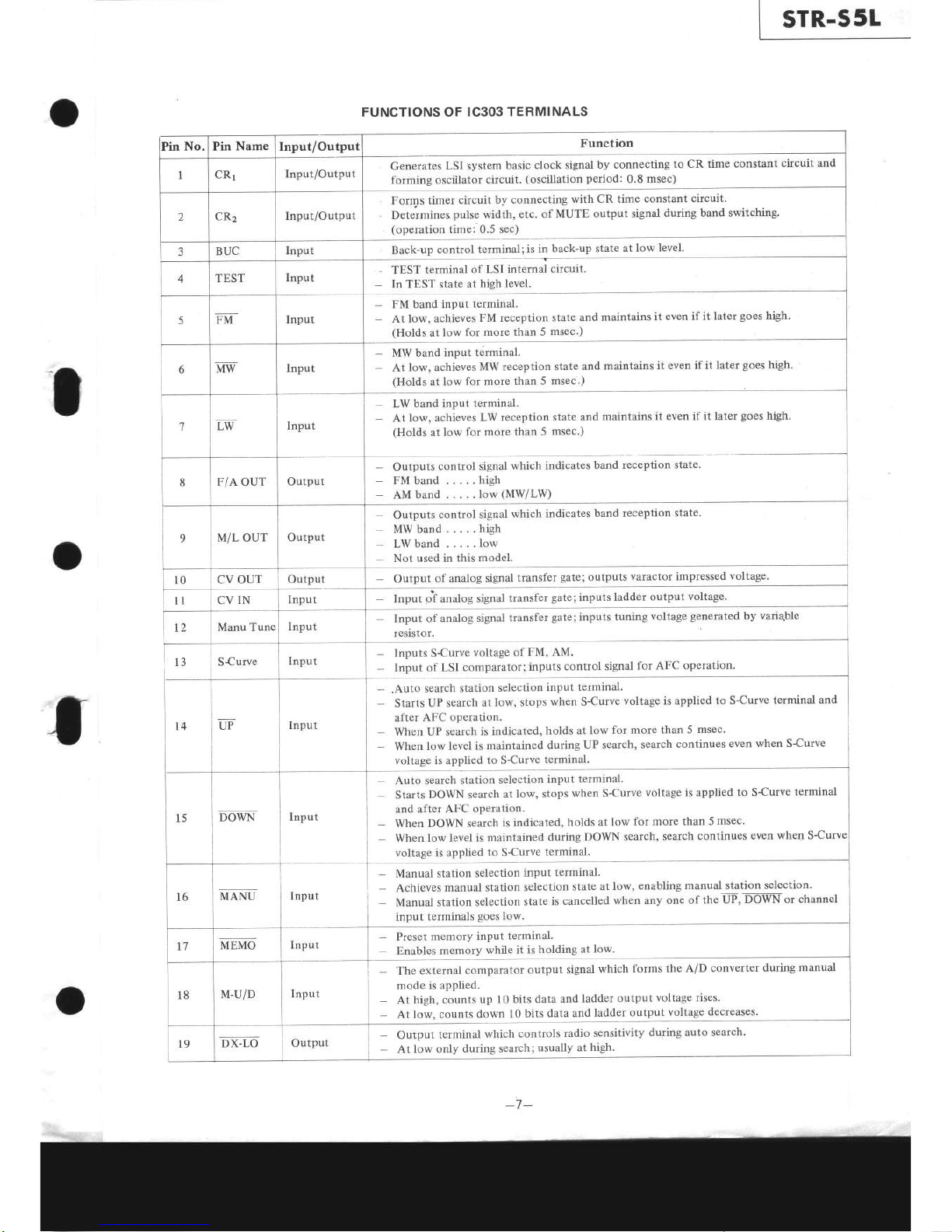
FUNCTIONS OF IC3O3
TERMINALS
I
S{urve
I
Input
DOWN
MANU
I
-
MEMO
Input
When UP search
is indicated,
holds at
low
for more than
5
msec.
when
low level
is maintained
during
uP
search,
search
continues
even when s{urve
voltage
is
applied
to S-Curve
terminâI.
Auto search
station
selection
input
terminal.
Starts
DOWN search
at
low, stops
when S-Curve
voltage is applied
to S{urve
terminal
and
after
AFC operation.
When
DOWN search
is
indicated,
holds at low
for more than 5
msec'
when low level
is maintained
during
DowN search,
search
continues
even
when
s-curve
I
-
Manual station
selection
state
is cancelled
when any
one of
the UF,DôWN
or
channel
input terminals
goes
low.
-
Preset memory
input
terminal.
-
Enables memory
while it
is
holding at
low.
-
The
external
comparator
output signal
which
forms the
A/D convertel
during
manual
mode
is applied.
-
At
high, counts
up 10
bits
data and
ladder output
voltage rises.
At low. counts
down
10
bits data
and
ladder
output
voltage
decreases.
Output
terminal
which
controls
radio
sensitivity
during auto search.
At
low only
during search;
usually
at
high.
;T*-
Pin No. Pin
Name
Input/Output
Function
I
CRr
Input/Output
Generates
LSI system
basic clock
signal
by connecting
to
CR time
constant
circuit and
forming oscillator
circuit.
(oscillation
period:
0.8
msec)
2
CRz
Input/Output
Forms
timer
circuit
by connecting
with
CR time
constant
circuit.
Determines
pulse
width,
etc. of
MUTE output signal
during band
switching.
(operation
time:
0.5
sec)
J
BUC
Input
Back-up
control
terminal; is
in
back-up state
at
low level
TEST
Input
TEST
terminal
of LSI
internal
circuit.
In
TEST state
at
high level.
f
FM
Input
FM band input
terminal.
At low, achieves
FM reception
state
and maintains
it even if
it later
goes
high.
(Holds
at low
for more than 5
msec.)
6
MW
Input
MW band
input terminal.
At
low, achieves
MW reception state
and
maintains
it even if it
later
goes
high
(Holds
at
low for more
than 5
msec.)
7
LW
Input
LW
band input
terminal.
At low,
achieves LW
reception
state and
maintains
it even if it
later
goes
high.
(Holds
at low
for more
than 5
msec.)
8
F/A
OUT
Outpu
Outputs
control signal
which indicates
band
reception state.
FM band . ....
high
AM band
low
(MW/LW)
lo
M/L OUT
Output
Outputs
control signal
which indicates
band reception
state.
MWband.....high
LW band .
.... low
Not used in this
model.
l0
CV OUT
Output
Output
of analog
signal
transfer
gate;
outputs
varactor impressed
voltage.
Input
qi
analog signal
transfer
gate;
inputs
ladder
output
voltage.
11
CV
IN
lnput
t2
Manu Tune
Input
Input of analog
signal
transfer
gate;
inputs
l:"19,'
Inputs S-Curve
voltage
of
F-M, AM.
tuning
voltage
generated
by
vari4ble
-
Input of LSI
comparator;
inputs
control signal
for AFC operation'
.Auto
search
station
selection
input terminal'
Starts
UP search
at
low, stops
when S-Curve
voltage is applied
to S-curve terminal
after
AFC
operation.
-7-
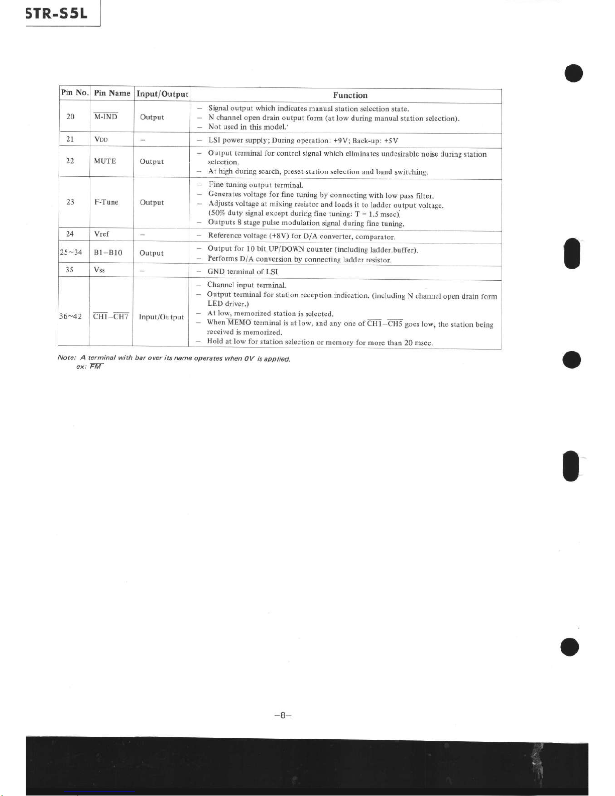
Pin
No.
Pin Name
Input/Output
Function
20 M-IND
Output
Signal output which
indicates
manual
station selection
state.
N
channel
open drain
output form
(at
low
during manual station
selection).
Not
used
in this model.'
2l
Vnl
-
LSI
power
supply; During operation:
+9V;
Back-up:
+5V
22
MUTE
Outpul
-
Output
terminal for control
signal which eliminates
undesirable
noise during
station
selection.
-
At high during
search,
preset
station selection
and band
switching.
ZJ F-Tune
Output
Fine
tuning
output
terminal.
Generates
voltage
for
fine
tuning
by connecting
with
low
pass
filter.
Adjusts
voltage
at mixing
resistor
and loads
it
to ladder
output
voltage
(50%
duty
signal except
during
fine
tuning:
T
=
1.5 msec).
Outputs
8 stage
pulse
modulation
signal
during fîne
tuning.
24 Vref
-
Reference
voltage
(+8V)
for
D/A
converter,
comparator.
25-34 Bl-Bl0
Output
Output for
l0 bit-
UP/DOWN
counter
(including
ladder.buffer).
Performs
D/A
conversion
bv connectins
ladder resistor.
3s
Vss
-
GND terminal
of LSI
36-42
CHl_CH7
Input/Output
Channel
input
terminal.
output
terminal for
station reception
indication.
(including
N channel
open
drain form
LED
driver.)
At low,
memorized
station
is
selected.
when
MEMô
terminal
is
at low.
and any one
of
cFI
t
-cH5
goes
low,
the station
being
received
is memorized.
Hold
at low for
station
selection
or memory for
more
than 20 msec.
Note: A
ex:
terminal with
bar over its name
operates when
OV is
apptied.
Fil,_
-8-
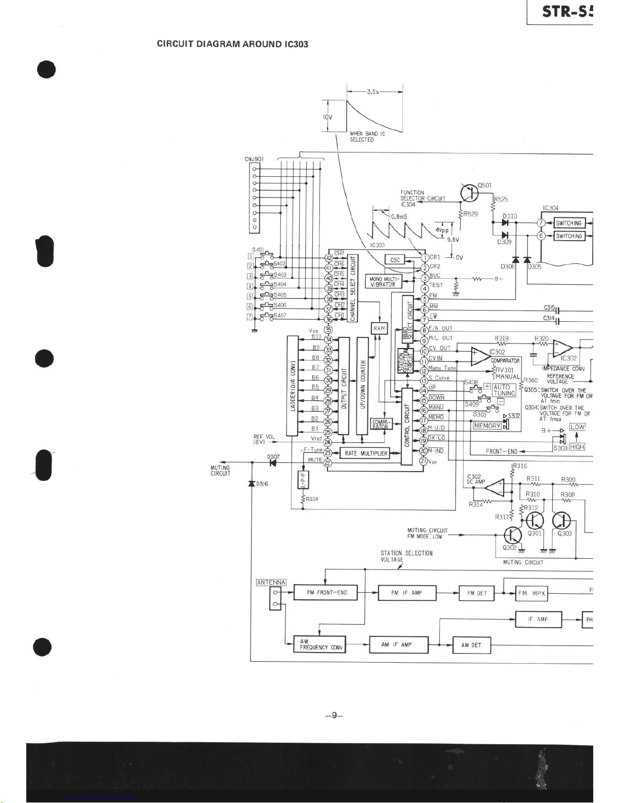
CIRCUIT
DIAGRAM
AROUND IC3O3
l_-l
|.--r'rs-+]
F\I
il>-l
STATION
VOLTAGT
FUNCTION
SETEC
rc304
0,8mS
---T---r
+vtp
I
9.5V
-l
ou
R319
R3
17
ioi
FrcHl
| 1
"',*t
I
|MPE0aNCE
CoNV
I
REFERINCE
I
JOU
VOLTAGE
+
,n__o
w
__rÈl I
O3O5:SWIÎCH
OVER THE
VOLTAGE
FOR
FM
OR
AT
fmin
Q3O4:SWITCH
OVER THE
VOLTAGE FOR
FM
OR
AT
fmor
rc302
OC AMP
MUTING
CIRCUIT
FI,| MODÊ:
LOW
SELEC TION
WHEN
BAND
IS
SELECTTO
z
J
-9-
STR.S5L
0306
8+
FOR MW
B+
FOR
LW
B+
FOR
FM
-10-
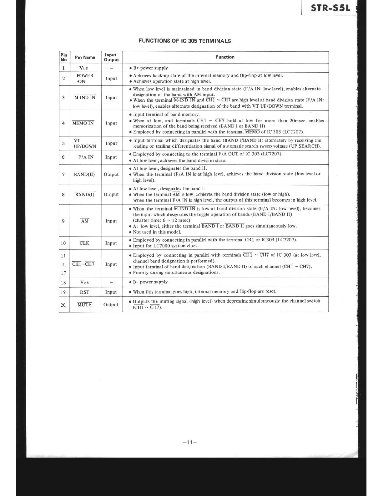
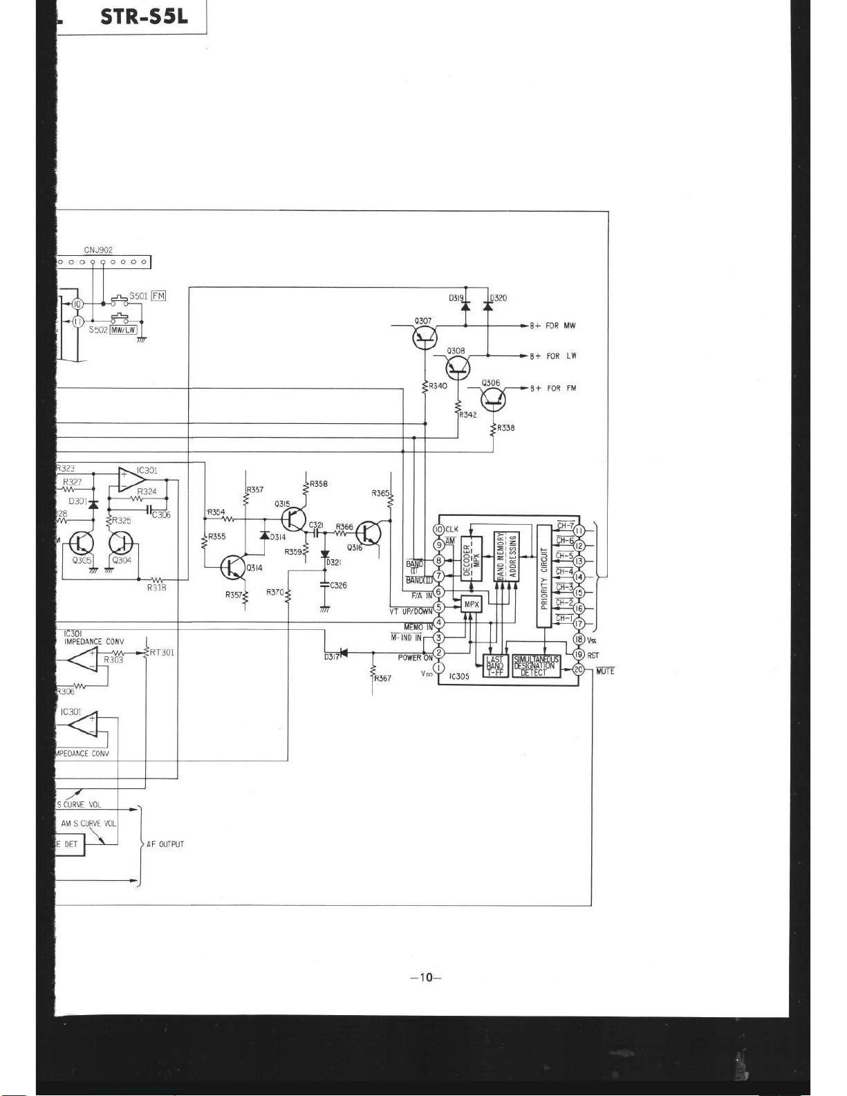
FUNCTIONS
OF IC
305 TERMINALS
Pin
No
Pin Name
Input
Outpul
Function
I Vno
.
B+
power
supply
2
PO\ryER
.oN
Input
o
Achieves back-up state of the internal
memory and flip-flop at low level.
o
Achieves operation
state at
high level.
3
I!-il.{D IN lnput
o
When low level is maintained
in band division state
(F/A
IN:
low level),
enables
alternate
designation of the band
with AM
input.
o
When the
terminal
M-IND IN
and
CHI - CH7 are high level at band division state
(F/A
IN:
low level),
enables
alternate designation
of
the band with VT
UPiDOWN
terminal.
4 MEMO IN
Input
.
Input terminal of band memory.
o
When at low,
and terminals eHl
-
CH7 trotd at low for more
than 2Omsec, enables
memorization of the band being received
(BAND
I or BAND II).
o
Employed by connecting in
parallel
with the terrninal
MEMO of IC
303
(LC'1207).
5
w
uP/DOWN
Input
.
Input terminal
which
designates the
band
(BAND
I/BAND II)
alternately by receiving
the
leading
or
trailing
differentiation signal of automatic search sweep
voltage
(UP
SEARCH).
6
F/A IN Input
r
Employed by connecting to the
terminal
F/A
OUT
of IC
303
(LC72O7).
.
At
low level, achieves
the band division state.
BAND-(ii)
Output
o
At low level,
designates
the band II.
r
When
the terminal
(F/A
IN
is at
high level, achieves
the band
division stâte
(low
level
or
high
level).
8
BAND(I)
Output
.
At low level, designates
the
band I-
.
When
the terminal
AM
is
low, achieves
the
band
division state
(low
or high).
When the terminal
F/A IN is high
level, the output of this terminal becomes in
high level.
9
AM
Input
r
When the terminal
Ni:IND-TN
is
low at band division state
(F/A
IN:
low level), becomes
the input
which
designates
the toggle operation
of
bands
(BAND
I/BAND II)
(chatter
time:
6 - 12
msec)
.
At
low level, either the terminalEÂNDI-orBA-ND-lf
goes
simultaneously low.
o
Not used in this model.
10
CLK
Input
o
Employed by connecting
in
paraÏel
with the
terminal CRI or IC303
(LC7207).
o
Input for LC7000 system clock.
11
l,
t'l
cHl-CH7
Input
o
Employed by connecting in
parallel
with terminals CHI - CH7
of IC
303
(at
low level,
channel band
designation is
performed)
.
Input terminal of
band designation
(BAND
I/BAND
II)
of each channel
(CH1
-
CH7).
o
Priority during simultaneous
designations.
18
Vss
o
B-
power
supply
t9
RST
Input
.
When
this terminal
goes
high, internal
memory and
flip-flop are
reset.
20
MUTE
Output
.
Outputs
the
muting signal
(high
level)
when depressing
simultaneously
the channel
switch
(cHl
-
cH7).
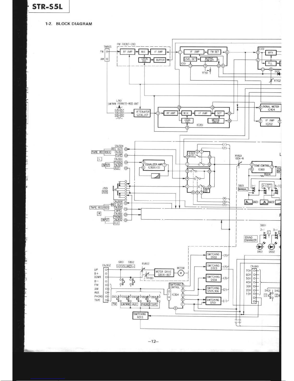
sTR-S5L
1.2. BLOCK DIAGRAM
FII,,I FRONT_END
r-----
----]
L90l
LW/MW
FERRITE
'.âr
o(il)o
-8irB"iie
tr
s80r
s802
Em-L!rv'-ËlE
UP
B+
DOWN
8-
FM
AM
AUX
"o{
@
SWITCHING
8504
SWTCHING
0505,506
SUTCHING
0313
-12-
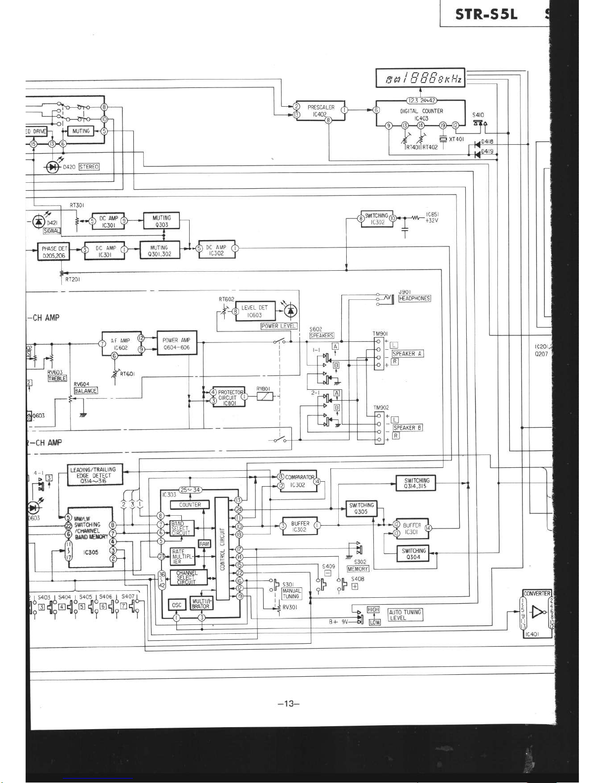
STR-S5L
rxltEEexH,
t
E
)
ts
z
SWITCHING
0305
rR-s5L
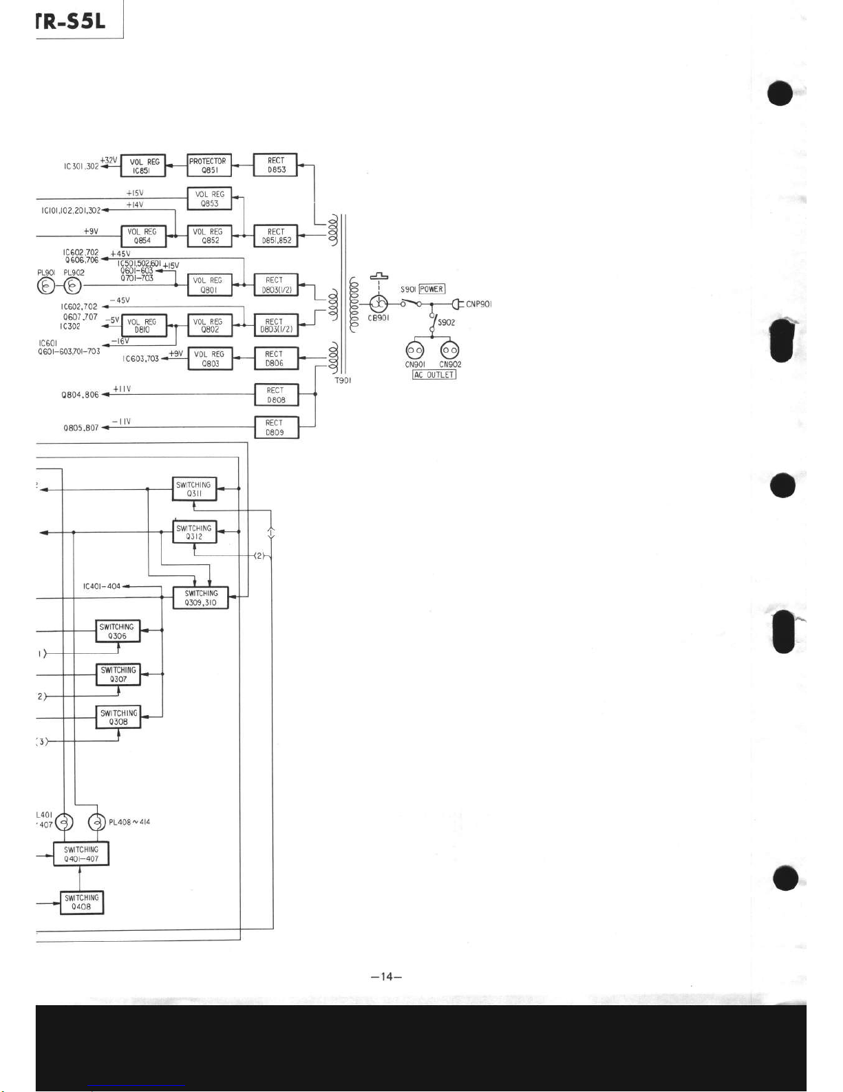
rc602,702
0607,707
I
c302
lc60r
Q60r-603,701-703
0804,806
0805,807
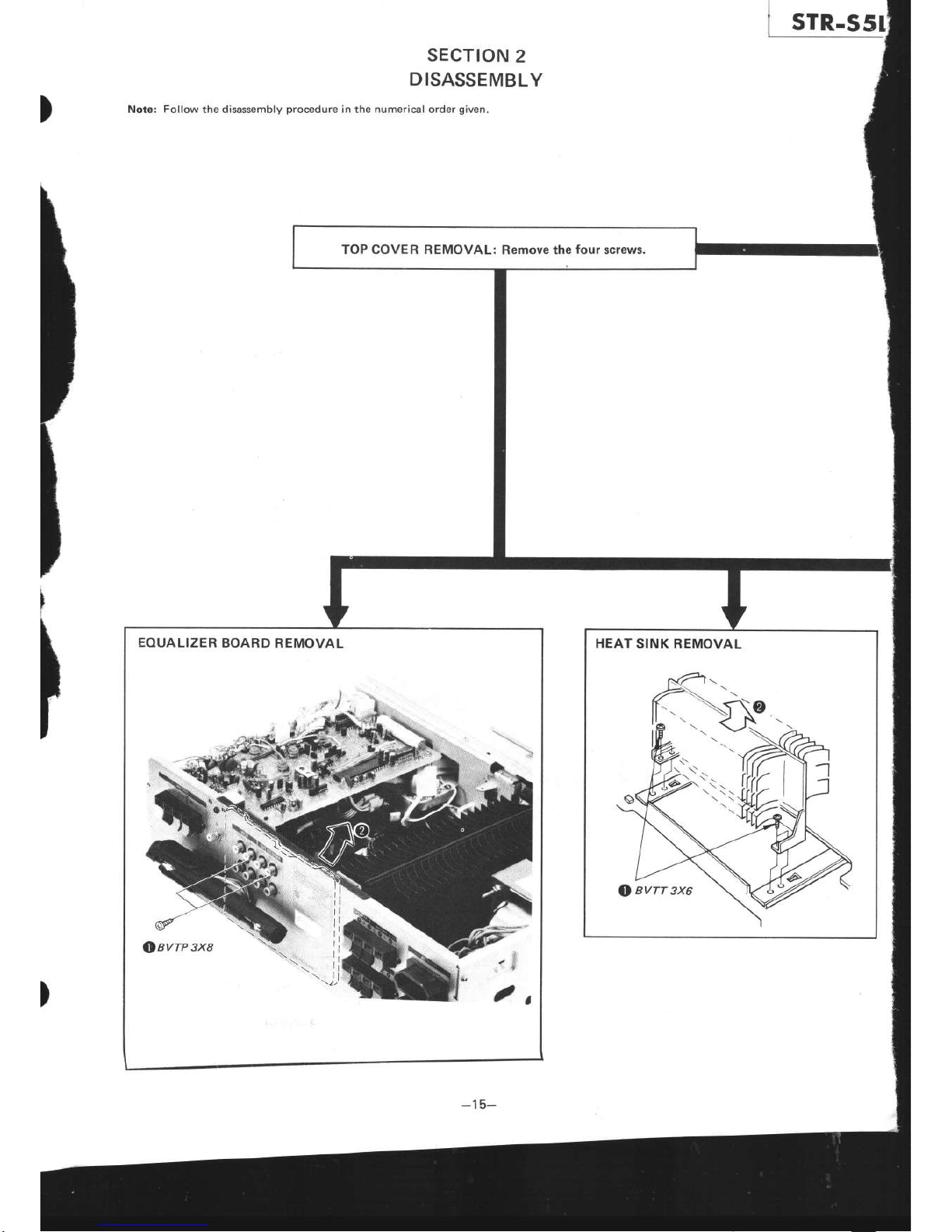
sTR-S5
TOP COVER REMOVAL:
Remove
the
four
screws.
EOUALIZER
BOARD REMOVAL
HEAT
SINK REMOVAL
)
SECTION
2
DISASSEMBLY
Note:
Follow
the
disassembly
procedure
in the numerical order
given.
I
I
)
-15-
 Loading...