

Page 1
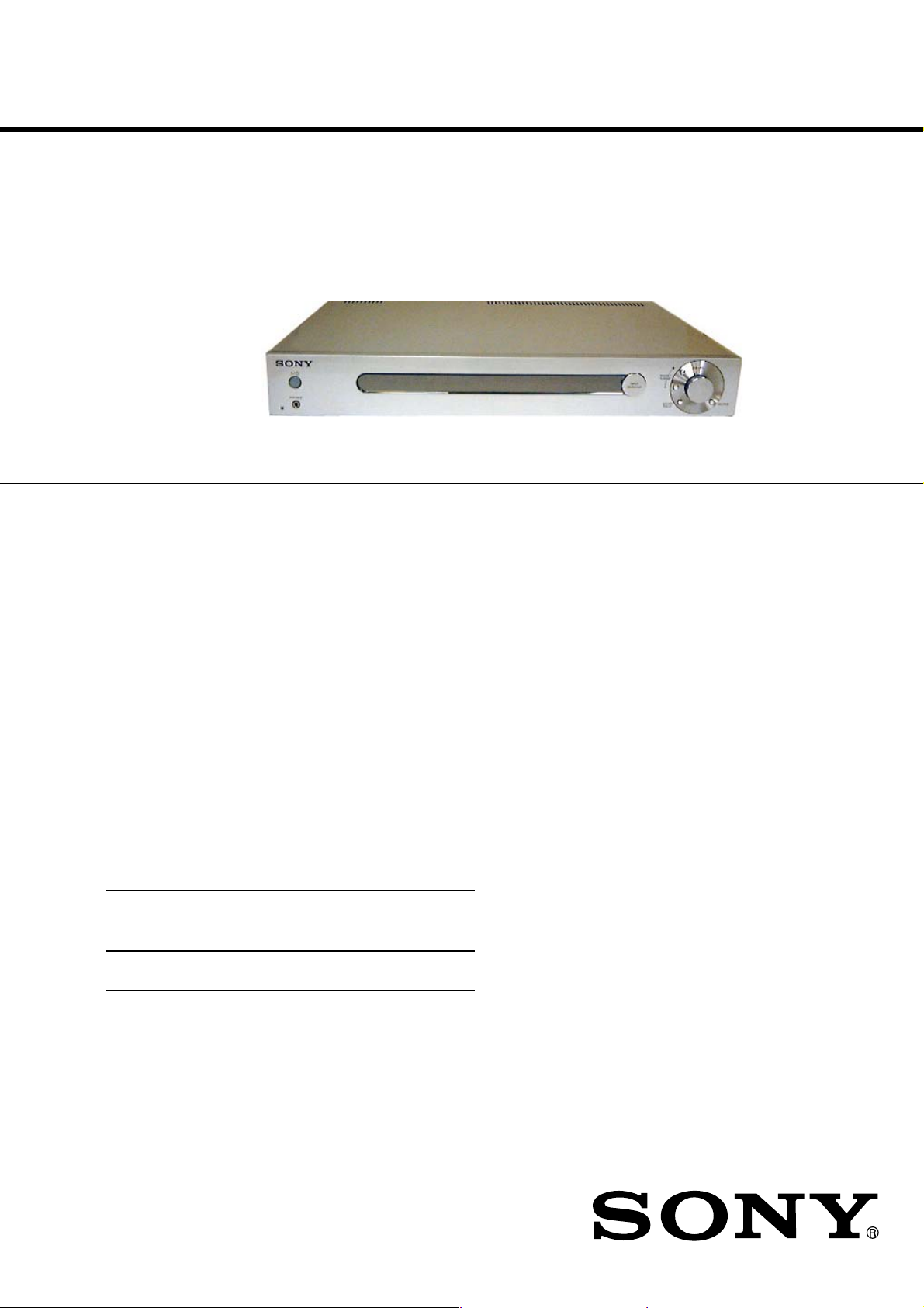
STR-LV700R
SERVICE MANUAL
Ver 1.2 2004. 06
Manufactured under license from Dolby Laboratories.
“Dolby”, “Pro Logic” and the double-D symbol are
trademarks of Dolby Laboratories.
“DTS” and “DTS Digital Surround” are trademarks of Digital
Theater Systems, Inc.
SPECIFICATIONS
Amplifier section
POWER OUTPUT
Rated power output in stereo mode
(8 Ω 1 kHz, DIN) 50 W + 50 W
Reference power output
(4 Ω 1 kHz, DIN) FRONT1): 75 W/ch
1)
Depending on the sound field settings and the source, there may be no
sound output.
Frequency response 20 Hz – 20 kHz
DVD, TV/SAT, HDD/MD Sensitivity: 500 mV
Inputs (analogue) Impedance: 50 kΩ
DVD, TV/SAT, HDD/MD S/N2): 84 dB
2)
Input short.
3)
Weighted network, input level.
Inputs (digital)
DVD (coaxial) Impedance: 75 Ω
DVD, TV/SAT, S/N: 90 dB
HDD/MD (optical) (A, 20 kHz LPF)
Sampling frequency
COAX, OPT 96 kHz
Outputs
LINE (subwoofer) Voltage: 2 V
CENTER1): 75 W
SURROUND1):75 W/ch
(A, 500 mV3))
S/N: 90 dB
(A, 20 kHz LPF)
Impedance: 1 kΩ
AEP Model
UK Model
FM tuner section
Tuning range 87.5 – 108.0 MHz
Antenna terminals 75 Ω, unbalanced
Intermediate frequency 10.7 MHz
Sensitivity
Mono: 18.3 dBf, 2.2 µV/75 Ω
Stereo: 38.3 dBf, 22.5 µV/75 Ω
Useable sensitivity 11.2 dBf, 1 µV/75 Ω
S/N
Mono: 76 dB
Stereo: 70 dB
Harmonic distortion at 1 kHz
Mono: 0.3%
Stereo: 0.5%
Separation 45 dB at 1 kHz
Frequency response 30 Hz – 15 kHz,
+0.5/–2 dB
Selectivity 60 dB at 400 kHz
AM tuner section
Tuning range 531 – 1,602 kHz
Antenna Loop antenna
Intermediate frequency 450 kHz
Usable sensitivity 50 dB/m (at 999 kHz)
S/N 54 dB (at 50 mV/m)
Harmonic distortion 0.5% (50 mV/m, 400 Hz)
Selectivity
At 9 kHz: 35 dB
– Continued on next page –
FM STEREO
9-961-435-03
2004F02-1
© 2004.06
FM-AM RECEIVER
Sony Corporation
Home Audio Company
Published by Sony Engineering Corporation
Page 2

STR-LV700R
Ver 1.1
Video section
Input
VIDEO: 1 Vp-p 75 Ω
Output
MONITOR: 1 Vp-p 75 Ω
Network Media section
Hardware decoder
MPEG2
Maximum 8 Mbps, 720 x 480 pixels, 30 fps
MPEG1
1.41 Mbps, 352 x 240 pixels, 30 fps
Playable file formats
Giga Pocket video
MPEG2, MPEG1
SonicStage music
ATRAC3, ATRAC3plus,WAV, MP3. WMA is
not supported.
Photo Server images
BMP, TIFF, GIF, JPEG,PNG
Interface
Network
100Base-TX
Compatible computers
VAIO computers bought after October 2003,
running Windows XP
Professional or Windows
XP Home Edition
General
Power requirements 230 V AC, 50/60 Hz
Power consumption 95 W
Dimensions 430 x 65 x 288 mm
including projections and controls
Mass (approx.) 3.2 kg
Package contents
AM loop antenna (1)
Allen screwdriver (1)
Connection adapter (1)
Cross-wired cable (1)
FM wire antenna (1)
Network cable (approx. 170 cm, 1)
Network cable ferrite core (1)
R6 (AA) batteries (2)
Remote control (RM-U70R)(1)
Speaker cable ferrite core (2)
Speaker plug (5)
Design and specifications are subject to change without notice.
TABLE OF CONTENTS
Specifications ............................................................................ 1
1. GENERAL...................................................................... 3
2. SERVICING NOTES................................................... 4
3. TEST MODE ................................................................. 7
4. DIAGRAMS
4-1. IC Pin Function Descriptions ................................ 13
4-2. Block Diagrams – Tuner/DSP Section –...............18
Block Diagrams – Display/Power Section –.........19
4-3. Printed Wiring Boards
– Digital Section (Side A)– ................................... 20
Printed Wiring Boards
– Digital Section (Side B)– ...................................21
4-4. Schematic Diagram – Digital Section (1/3)–........22
4-5. Schematic Diagram – Digital Section (2/3)–........23
4-6. Schematic Diagram – Digital Section (3/3)–........24
4-7. Schematic Diagram – Amp Section (1/2)– ........... 25
4-8. Schematic Diagram – Amp Section (2/2)– ........... 26
4-9. Printed Wiring Boards – Amp Section–................27
4-10. Schematic Diagram – Display Section– ............... 28
4-11. Printed Wiring Boards – Display Section– ...........29
4-12. Schematic Diagram – Power Section–..................30
4-13. Printed Wiring Boards– Power Section– .............. 31
4-14. IC Block Diagrams ................................................ 32
5. EXPLODED VIEWS
5-1. Front Panel Section ................................................. 33
5-2. Cabinet Section........................................................ 34
6. ELECTRICAL PARTS LIST ....................................35
Unleaded solder
Boards requiring use of unleaded solder are printed with the leadfree mark (LF) indicating the solder contains no lead.
(Caution: Some printed circuit boards may not come printed with
the lead free mark due to their particular size.)
SAFETY-RELATED COMPONENT WARNING!!
COMPONENTS IDENTIFIED BY MARK 0 OR DOTTED LINE
WITH MARK 0 ON THE SCHEMATIC DIAGRAMS AND IN THE
PARTS LIST ARE CRITICAL TO SAFE OPERATION. REPLACE
THESE COMPONENTS WITH SONY PAR TS WHOSE PART NUMBERS APPEAR AS SHOWN IN THIS MANUAL OR IN SUPPLEMENTS PUBLISHED BY SONY.
2
: LEAD FREE MARK
Unleaded solder has the following characteristics.
• Unleaded solder melts at a temperature about 40°C higher than
ordinary solder.
Ordinary soldering irons can be used but the iron tip has to be
applied to the solder joint for a slightly longer time.
Soldering irons using a temperature regulator should be set to
about 350°C.
Caution: The printed pattern (copper foil) may peel away if the
heated tip is applied for too long, so be careful!
• Strong viscosity
Unleaded solder is more viscous (sticky, less prone to flow)
than ordinary solder so use caution not to let solder bridges
occur such as on IC pins, etc.
• Usable with ordinary solder
It is best to use only unleaded solder but unleaded solder may
also be added to ordinary solder.
Notes on chip component replacement
• Never reuse a disconnected chip component.
• Notice that the minus side of a tantalum capacitor may be damaged by heat.
Page 3
Main unit
1 2 354
67
8
Alphabetical order
Display 2
INPUT SELECTOR 3
MUTING 6
PHONES jack 8
PRESET TUNING +/– 4
SOUND FIELD 7
VOLUME 5
SECTION 1
GENERAL
Symbols
?/1 (power) 1
STR-LV700R
This section is extracted
from instruction manual.
3
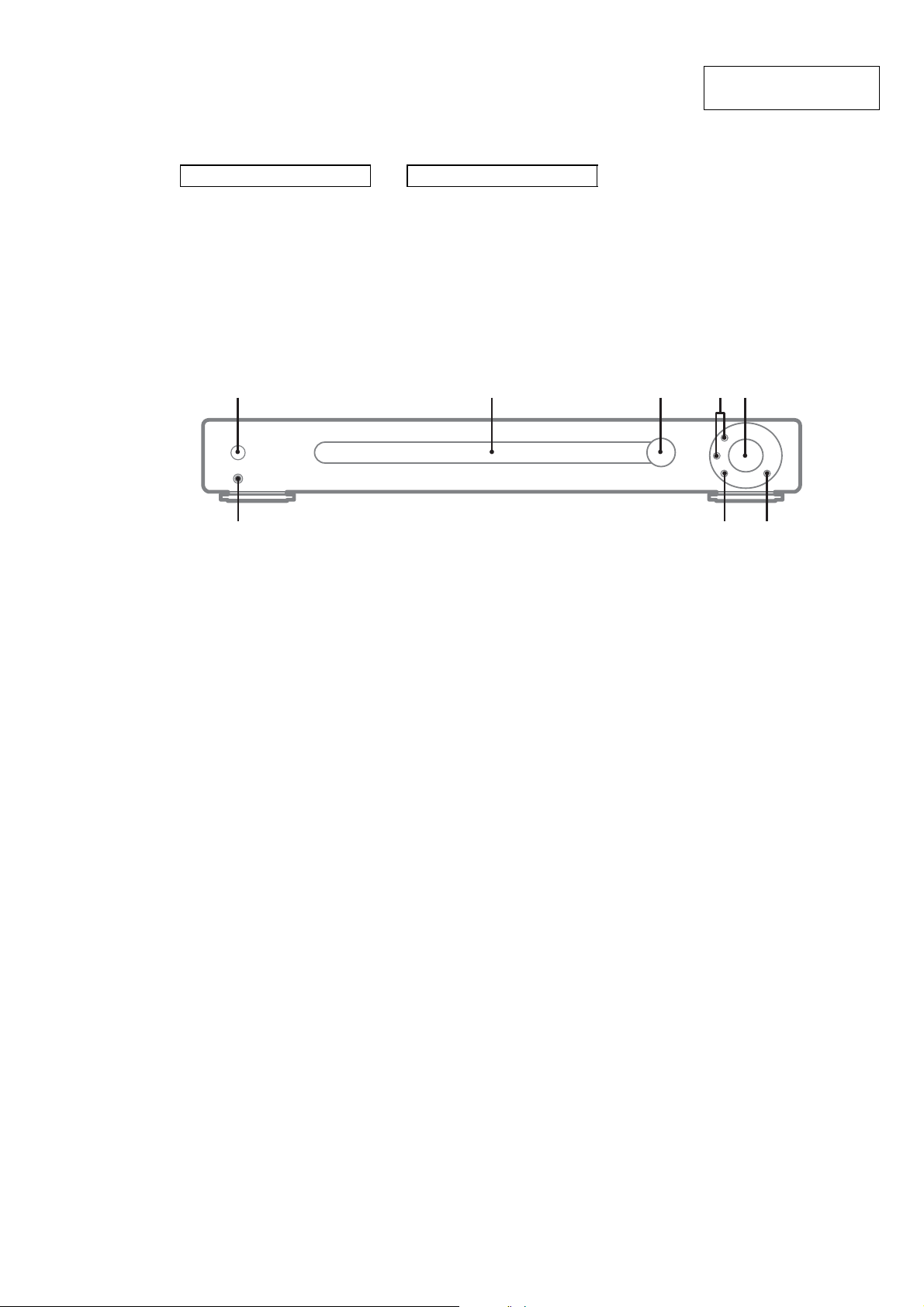
Page 4
STR-LV700R
t
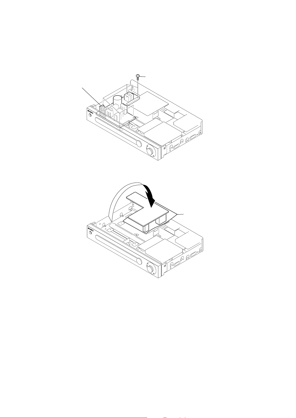
SERVICE POSITION
• POWER BOARD
POWER board
SECTION 2
SERVICING NOTES
1
remove five screws
(+BVTP 3x8)
2
isolation shee
4
Page 5
• VIDEO, DIG-IN, DIGITAL BOARD
9
DIG-IN board
7
VIDEO board
2
tuner unit
STR-LV700R
8
five screws
(+BVTP 3x8)
6
three screws
(+BVTP 3x8)
q;
three screws
(+BVTP 3x8)
1
three screws
(+BVTP 3x8)
5
VIF-20(EU) assy
qs
DIGITAL board
DIGITAL board
qa
four screws
(+BVTP 3x8)
3
two screws
(+BVTT 3x6)
DIG-IN board
VIF-20(EU) assy
qd
VIDEO board
4
two screws
(+BVTT 3x6)
isolation sheet
5
Page 6
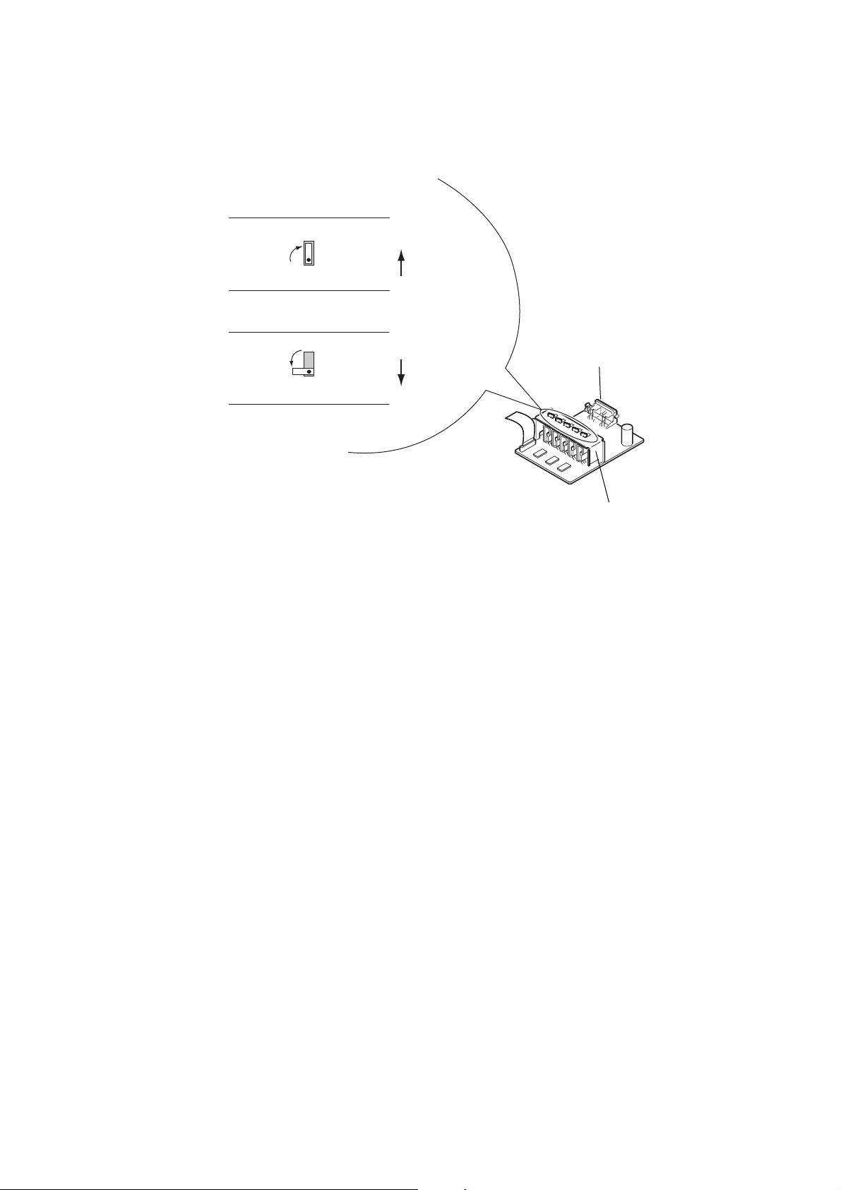
STR-LV700R
• AMP BOARD
• On Removal
1
Bend claws 90 degree
clokwise.
• On Attaching
2
Bend claws 90 degree
counterclokwise.
2
Slide up
the heat sink.
1
Slide down
the heat sink.
AMP board
heat sink.
6
Page 7

SECTION 3
TEST MODE
All test modes can be cancelled by turning the main power off.
[SOUND FIELD CLEAR MODE]
The preset sound field is cleared when this mode is selected.
(Use this mode before returning the product to the client after repairs have been completed.)
Procedure:
1. While depressing the SOUND FIELD button, press the =/1
button to turn the main power on.
2. The message “SF .CLR.” appears on the indicator and the sound
field mode is cleared.
[FACTORY SET MODE]
All preset modes are reset to the default settings.
Procedure:
1. While depressing the PRESET TUNING – button, press the
=/1 button to turn the main power on.
2. Press the ENTER (SELECT) button on the remote controller
3 times consecutively, then press the MAIN MENU button
followed by the A.F.D button.
3. The message “FACTORT” appears on the indicator tube and
all the modes are reset to the default settings.
[ALL CLEAR MODE]
All the preset values are cleared when this mode is selected.
STR-LV700R
[FLUORESCENT INDICATOR TUBE TEST MODE]
All fluorescent indicator segments are tested in this mode.
Procedure:
1. While depressing the PRESET TUNING – button, press the
=/1 button to turn the main power on.
2. Press the ENTER (SELECT) button on the remote controller
3 times consecutively, then press the MAIN MENU button
followed by the M button.
3. All the fluorescent indicator segments turn on.
4. Each time the VIDEO button is pressed, the segments are
turned on and off in the following order.
Half of the segments turn on t the remaining half turn on
t all segments turn off t all the segments turn on.
[DSP TEST MODE]
Procedure:
1. Press the =/1 button to turn the main power on.
2. Press the ENTER (SELECT) button on the remote controller
3 times consecutively, then press the MAIN MENU button
followed by the MUTING button.
3. “SWP.NORM” appears on the indicator and the DSP mode is
set.
• Select the item by pressing the cursor button M or m .
• Select the function by pressing the cursor button < or , .
Procedure:
1. While depressing the PRESET TUNING – button, press the
=/1 button to turn the main power on.
2. Press the ENTER (SELECT) button on the remote controller
3 times consecutively, then press the MAIN MENU button
followed by the , button.
3. The message “CLEARED” appears on the indicator tube and
all the preset values are cleared. After the backup operation is
completed, the main power turns off automatically.
[SOFTWARE VERSION DISPLAY MODE]
The software version is displayed.
Procedure:
1. While depressing the PRESET TUNING – button, press the
=/1 button to turn the main power on.
2. Press the ENTER (SELECT) button on the remote controller
3 times consecutively, then press the MAIN MENU button
followed by the < button.
3. The software version is displayed (for example, “LSR CE
0.04”) on the indicator tube.
[KEY CHECK MODE]
The buttons are checked in this mode.
Procedure:
1. While depressing the PRESET TUNING – button, press the
=/1 button to turn the main power on.
2. Press the ENTER (SELECT) button on the remote controller 3 times consecutively, then press the MAIN MENU button followed by the m button.
3. The message “REST 05” appears on the indicator tube.
4. To start the countdown, press any button (other than the =/1
button).
The buttons which have been already counted are not recounted.
5. After all the buttons to be counted been pressed the message
“REST 00” is displayed. This completes the key check operation.
7
Page 8
STR-LV700R
Items
SWAP
DSP Version
DSP communication
Bass Management
Main Speaker cut off Freq.
LFE cut off Freq.
Co-ef. Read Address
Co-ef. Read Data
Co-ef. Write Address
Co-ef. Write Data
SRAM
Total operation time
Longest Power ON time
Output time less than
–50dB volume
Output time less than
–40dB volume
Output time less than
–30dB volume
Output time less than
–20dB volume
Output time less than
–10dB volume
Output time less than
0dB volume
Protector count value
Fuse open count value
EEPROM CONDITION
EEPROM READ
EEPROM Super Reset
DSP HALT MODE
Function
NORM
ALL
C SW
SLSR
–
–
–
–
–
–
–
–
–
OFF
ON
–
–
–
–
–
–
–
–
–
–
–
–
–
–
Description
Normal channel output
Left input t Front Left, Surround Left, Center channel output
Right input t Front Right, Surround Right, Sub Woofer channel output
Left input t Center channel output
Right input t Sub Woofer channel output
Left input t Surround Left channel output
Right input t Surround Right channel output
“DSPV XXX” is displayed. Three large charactors are the dsp version that
is being used.
When this item is selected the message will be displayed “ OK ” if the
checking is correct. “ ERROR ” will be displayed in a case of an error.
Not used for service
Not used for service
Not used for service
Not used for service
Not used for service
Not used for service
Not used for service
“ RAMC. OFF ” will be displayed in a case of no checking.
By pressing Cursor button the checking starts.
“ RAMC. PASS ” will be displayed if the checking is good.
“ RAMC. NG ” will be displayed if an error occurs.
TTL-XXXX xx is displayed.
LNG-XXXX xx is displayed.
V50-XXXX xx is displayed.
V40-XXXX xx is displayed.
V30-XXXX xx is displayed.
V20-XXXX xx is displayed.
V10-XXXX xx is displayed.
V00-XXXX xx is displayed.
PROTXXXX xx is displayed.
FUSEXXXX xx is displayed.
E- XXXX is displayed.
S RST t Super Reset : first time use EEPROM or test pattern
corrupted
FAIL t EEPROM read / write with microcom has problem
V CHG t Software version change
D CHG t Destination / model change
CLEAR t Back up data initialize
NORM t Normal AC on
E- XXX-XX is displayed.
First four hex code is EEPROM address (controlled by +/– button).
Last two hex code is EEPROM data.
S.RST- XXX is displayed.
When YES is selected, press Cursor button to clear all EEPROM data
HALT NO or HALT YES is displayed.
Remark
Selection of setting
output channels
Checking communication
between DSP and microcom
Checking communication
between DSP and SRAM
Four large charactors are
hour. Two small charactors
are minutes.
0 to 255
8
Page 9
STR-LV700R
Ver 1.1
How To Upgrade the Firmware Version
The following is the method of upgrading the control software (firmware) preinstalled in the STR-L V700R to the latest version. Note that
this method should only be employed when the software version is upgraded.
Note: The firmware version installed in the STR-LV700R as of October 2003 is 1.0.3.
Before executing this procedure, check to make sure that the preinstalled software version will not be downgraded to older version.
The latest information on the software version can be found in the “STR-L V700R Support Information” at http://www.vaio-link.com /info/lv700R/
EN.
1. Preparation and setup of Vaio
1. Items required for writing the firmware
• Vaio for testing
VAIO computer models marketed from October 2003 running Windows XP Professional or Windows XP Home Edition.
Functions depend on the model of VAIO computer connected.
VAIO computer models marketed from October 2003
Models Models with Giga Pocket Models without Giga Pocket
Supported PCV-W series PCS-RS3 series without
functions PCV-RZ4 series Giga Pocket
PCV-RS3 series All Sony Notebooks with
VAIO Media
Music playback Yes
Photograph viewing Yes
Video playback Yes No
Television viewing and
recording
Yes No
Notes
• VAIO computer models marketed before October 2003 do not support the functions above.
• Depending on the configuration of your VAIO computer, there may be some operation restrictions. For details about these
restrictions and up-to-date information, visit the Sony home audio customer support Web site at http://www.vaio-link.com/info/
lv700R/EN/
• Test program disk (J-2501-266-A)
• STR-LV700R for writing firmware
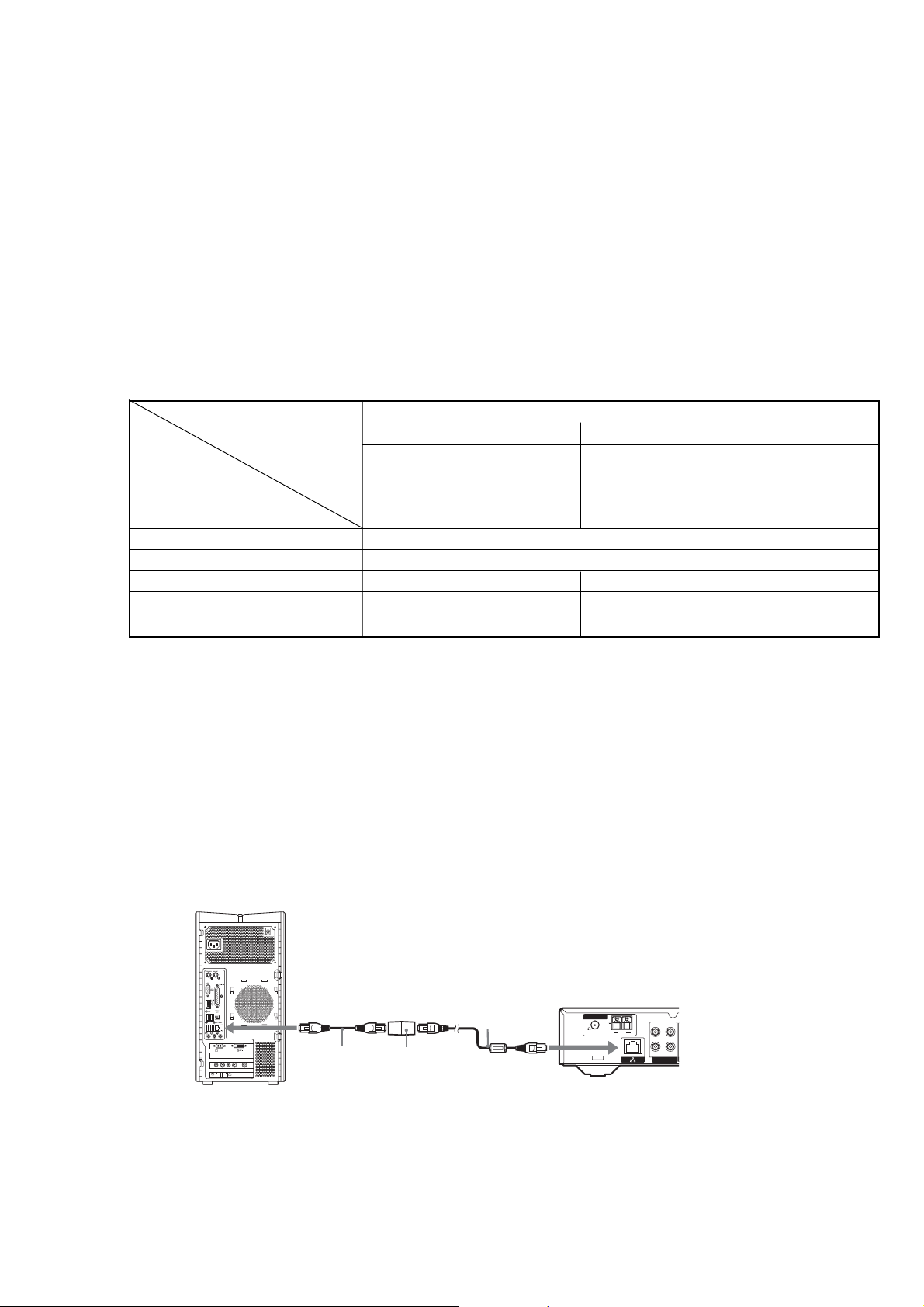
• Remote commander (accessory)
• The network cable, cross-conversion cable and the connection adaptor supplied as accessories (a 100BASE-TX cross cable can also be
substituted for these items).
• Television set with line input terminals (video and audio terminals)
2. Connect the STR-LV700R to the Vaio for testing using the network cable, adapter and cross-conversion cable (or use the 100BASE-
TX cross cable).
Attach the supplied ferrite core to the
supplied network cable before connecting
the cable to the receiver
MONITOR
USB
HEADPHONES
MIC
LINE IN
MONITOR
VHF/UHF
AUDIO
AUDIO
S VIDEO/VIDEO S VIDEO/VIDEO
–
–
–
–
VIDEO OUTPUT
VIDEO1 INPUT
LINEPHONE
VAIO computer
To Ethernet port
Crossover
cable
Connection
adapter
Network cable
with ferrite core
(supplied)
To Ethernet port
ANTENNA
U
75
FM
AM
STR-LV700R
L
R
OUT
IN
HDD/MD
Notes
• This connection method may vary depending on factors specific to your network.
• In this conection method the VAIO computer must have a fixed IP address for the LAN connection.
3. Setup the Vaio according to the procedure given on pages 30 to 33 of the Instruction Manual.
9
Page 10

STR-LV700R
Ver 1.2
2. Start up STR-LV700R with the Firmware Write Mode.
1. Start up the STR-LV700R and press the N.MEDIA button on
the remote controller to open the main menu on the television
screen.
2. Use the cursor buttons and ENTER (SELECT) buttons on
the remote controller, select “Settings” t “System Settings”
t “Firmware Update” t “OK.”
3. Writing firmware from the Vaio for testing
Upgrade the two types of firmware (ipls.bin and route66s.bin) to
the latest versions.
Note that this method should only be employed when the software
version is upgraded.
In cases when the firmware is downloaded from the home page,
also follow the procedure given below.
1. Check the version.
Start the STR-LV700R, then open the main menu and select
“Settings” t “System Settings” t “Device Information.”
Next, check that the firmware version.
2. Start up “EU-firm-1.XX” t “Updater.exe” from “Test JIG
Tool CD” (J-2501-266-A). (XXX indicates version)
3. Click the Update button to begin updateing firmware.
The message “Wait a few minutes until this screen turns off
and the Standby lamp lights” is displayed on the screen. With
this unit, when this step is completed, the network media function automatically restarts.
OPERATION CHECK METHOD
How to check the operation after repairing the main unit
or writing firmware
The following items are needed to perform the check:
•A device that is able of checking the environment during firm-
ware writing along with video and audio output terminals.
• The server application (Giga Pocket Server 5.0) needs to be in-
stalled in the Vaio for testing.
To perform the check, connect the Vaio with the preinstalled server
application to the STR-LV700R and check that the test video and
audio data are played and output correctly via the network.
1. Preparation
2. Preparation of the Vaio for Testing
Use the same Vaio used for writing firmware.
2-1. Insert the J-2501-266-A test program disk into the test Vaio.
2-2. Install the test color bar /1kHz signal from the test program
disk. Start the Giga Pocket Explorer . From the video capsule menu, select “Read” and then click “Browse…”. Select
“CD-ROM” t “75p1k1min” folder t “75p1k1min.mpg.”
Enter “COLOR-1KHZ” in the Video Capsule Name field and
then click the Run button.
Saved in “My Cabinet” of the Giga Pocket Explorer.
3. Setup the Vaio according to the procedure given on pages 30
to 33 of the Instruction manual .
4. Connect the outputs (video, audio, optical digital audio) from
the STR-LV700R to a television set and connect the device
with the optical digital input.
2. Testing method
1. Start up the STR-LV700R and press the N.MEDIA button on
the remote controller to open the main menu on the television
screen.
2. When the main menu is displayed on the television screen,
select “Video t Watch video clips” and press the ENTER
(SELECT) button.
3. When the servers list is displayed in the “Select Server Screen.”
From this list, select the name of the Vaio for testing and press
the ENTER (SELECT) button and select “Connect” in the
submenu. If the servers list does not appear even after a certain time interval has elapsed, press the OPTIONS button
on the remote controller to display the tool menu. In the tool
menu, select “Update to the latest information” and press the
ENTER (SELECT) button.
4. When the server is connected, the selection menu for all libraries is displayed. From this menu, select “My Cabinet” and
press the ENTER (SELECT) button.
5. When the video capsule selection menu is displayed, select
“COLOR-1KHZ.”
6. If color bars are displayed for video and 1kHz is output to
audio, the unit is functioning properly.
Also check the video output, audio output and optical digital
output items.
7. After the system has been completed, reset the STR-LV700R
to the factory preset values.
1. Items required for testing
• STR-LV700R to be tested.
• Test JIG Tool CD (J-2501-266-A)
• Remote commander (accessory)
• The network cable, cross-conversion cable and connection
cable supplied as accessories (a 100BASE-TX cross cable can
also be substitute for these items).
•AV cable
• Optical digital cable
•Television set with line input terminals (video and audio terminals)
• Device with optical digital input
10
Select “Setting” t “System Setting” t “Factory Default”
t “OK.”
Page 11
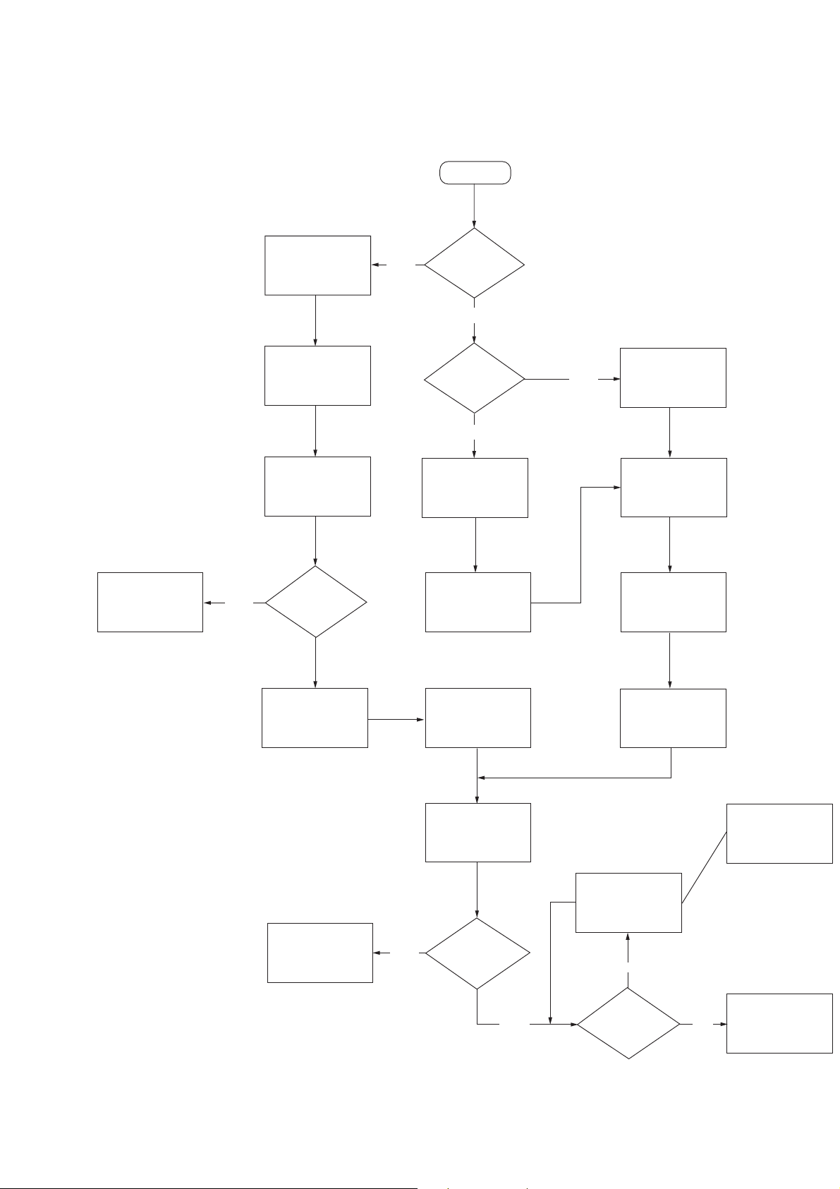
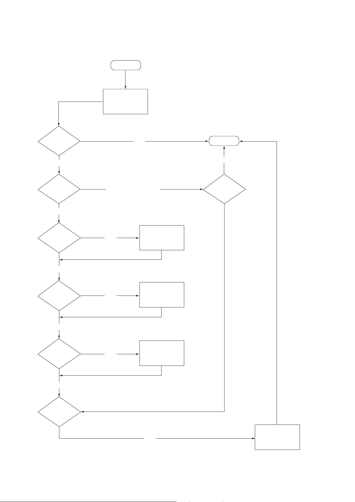
Setting up STR-LV700R
Start
Use router?
Confirm CAT 5
straight cable used
to connect both
VAIO and STR-LV700R
Is an IP address
retrieved correctly?
Use network
switch/hub
Confirm devices
are connected to
router using LAN
parts (not WAN)
Confirm crossover
cable is
used to connect
VAIO and STR-LV700R
Confirm fixed IP is
set for VAIO
(e.g.IP:169.254.xxx.xxx,
mask: 255.255.0.0)
Select “Obtain an IP
address automatically
(not using router)” in IP
address menu
Restart STR-LV700R
Confirm CAT 5
straight cable used
to connect both
VAIO and STR-LV700R
Confirm network
switch/hub is
powered on
Confirm “Obtain an IP
address automatically
(using router)” is select
in IP address Menu
Select any function
from Main Menu
on STR-LV700R
Push Option
button and select
Refresh
If no server appears on
the list after several
attempts, contact ITD
engineering for support
Try to connect to a
sever and confirm
whether other
function works
Obtain router make
and model info
from user
Confirm router is
turned on before
restart STR-LV700
Confirm router is
powered on and not
configured as a
network switch
Confirm VAIO is
set to use auto IP
Is an IP address
retrieved correctly?
Does any
server appear
on the list?
No
Yes
No
No
No
No
Yes
Yes Yes
Assuming user has configured VAIO
STR-LV700R
Ver 1.1
11
Page 12
STR-LV700R
Ver 1.1
Configuring V AIO
Start
Ask for VAIO
Model information
and confirm
firmware version
Is target
model?
Yes
Can connect to
any function?
No
Is personal
firewall
enabled?
No
Is access
allowed in VAIO
Media Console?
No
Except TV and Video
Yes
No
Stop
No
Is Giga
Pocket model?
Turn off personal
firewall
Enable accese
check box
12
Yes
Are all Servers
started?
Yes
Is Giga Pocket
Server started
and is
password set?
No
Start all servers
Yes
Restart your
computer
Page 13
4-1. IC Pin Function Descriptions
• IC115 CXD9617R (AUDIO DSP) (DIGITAL BOARD)
Pin No.
1
2
3
4
5
6
7
8
9
10
11
12
13
14
15
16
17
18
19
20
21
22
23 to 25
26
27
28
29
30
31
32
33
34
35
36
37
38
39
40
41
42
43
44
45
46
47
48
49
50
51
52
Pin Name
VSS
XRST
EXTIN
FS2
VDD1
FS1
PLOCK
VSS
MCLK1
VDD1
VSS
MCLK2
MS
SCKOUT
LRCKI1
VDDE
BCKI1
SDI1
LRCKO
BCKO
VSS
KFSIO
SDO1 to SDO3
SDO4
SPDIF
LRCKI2
BCKI2
SDI2
VSS
HACN
HDIN
HCLK
HDOUT
HCS
SDCLK
CLKEN
RAS
VDDI
VSS
CAS
DQM/OE0
CSO
WEO
VDDE
WMD1
VSS
WMD0
PAGE2
VSS
PAGE1
I/O
—
Ground terminal
I
Rest input from the system control
I
Not used (connected to ground)
I
Not used (connected to ground)
—
Power supply (+2.5V)
I
Not used (connected to ground)
O
Not used (open)
—
Ground terminal
I
Clock input (13.5MHz)
—
Power supply (+2.5V)
—
Ground terminal
O
Clock output (13.5MHz)
I
Not used (connected to ground)
O
Internal system clock output to CXD9743N
I
Sampling clock input from PCM1800E/2K
—
Power supply (+3.3V)
I
Bit clock input from PCM1800E/2K
I
Serial data input from PCM1800E/2K
O
Sampling clock output to CXD9743N
O
Bit clock output to CXD9743N
—
Ground
I
Audio clock (384fs/256fs) input from LC89056W
O
Serial data output to CXD9743N
O
Not used (open)
O
Not used (open)
I
Sampling clock input from LC89056W
I
Bit clock input from LC89056W
I
Serial data input from LC89056W
—
Ground
O
Acknowledge output to MB90F474HPF
I
Serial data input from MB90F474HPF
I
Clock input from MB90F474HPF
O
Serial data output to MB90F474HPF
I
Chip selection input from MB90F474HPF
O
Not used (open)
O
Not used (open)
O
Not used (open)
—
Power supply (+2.5V)
—
Ground
O
Not used (open)
O
Not used (open)
O
Chip selection output to the SRAM
O
Write enable output to the SRAM
—
Power supply (+3.3V)
I
Not used (connected to VDD)
—
Ground
I
Not used (connected to VDD)
O
Not used (open)
—
Ground
O
Not used (open)
STR-LV700R
SECTION 4
DIAGRAMS
Description
13
Page 14
STR-LV700R
Pin No.
53
54
55
56
57
58
59
60
61
62
63
64 to 66
67
68
69
70
71
72 to 75
76
77 to 80
81
82
83 to 85
86
87
88
89
90
91
92 to 97
98,99
100
101
102 to 105
106
107,108
109,110
111
112
113
114
115
116
117 to 119
120
Pin Name
PAGE0
BOOT
BTACT
BST
MOD1
MOD0
EXLOCK
VDDI
VSS
A17
A16
A15 to A13
GP10
GP9
GP8
VDDI
VSS
D15/GP7 to D12/GP4
VDDE
D11/GP3 to D8/GP0
VSS
A9
A12 to A10
TDO
TMS
XTRST
TCK
TDI
VSS
A8 to A3
D7,D6
VDDI
VSS
D5 to D2
VDDE
D1,D0
A2,A1
VSS
A0
PM
SD13
SD14
SYNC
VSS
VDDI
I/O
O
Not used (open)
I
Not used (connected to ground)
I
Not used (open)
I
Boot strap signal input from MB90F474HPF
I
Mode input (connected to VDD)
I
Mode input (connected to ground)
I
Lock signal input to LC89056W
—
Power supply (+2.5V)
—
Ground
O
Not used (open)
O
Not used (open)
O
Address bus output to the SRAM
I/O
Sampling clock I/O terminal
I/O
PCM/NON_PCM information signal I/O terminal
I/O
Bitstream information read enable signal I/O terminal
—
Power supply (+2.5V)
—
Ground
I/O
SRAM data bus
—
Power supply (+3.3V)
I/O
SRAM data bus
—
Ground
O
Address bus output to the SRAM
O
Address bus output to the SRAM
O
Not used (open)
I
Not used (open)
I
Not used (open)
I
Not used (open)
I
Not used (open)
—
Ground
O
Address bus output to the SRAM
I/O
SRAM data bus
—
Power supply (+2.5V)
—
Ground
I/O
SRAM data bus
—
Power supply (+3.3V)
I/O
SRAM data bus
O
Address bus output to the SRAM
—
Ground
O
Address bus output to the SRAM
I
PLL initialization input from MB90F474HPF
I
Not used (open)
I
Not used (open)
I
Synchronization / asynchronous selection input (pull up)
—
Ground
—
Power supply (+2.5V)
Description
14
Page 15

• IC118 MB90F474HPF-G-SOZ1398 (SYSTEM CONTROL) (DIGITAL BOARD)
Pin No.
1
2
3
4
5
6
7
8
9
10
11
12
13
14
15
16
17
18
19
20
21
22
23
24
25
26
27
28
29
30
31
32
33
34
35
36
37
38
39
40
41
42
43
44
45
46
47
48
49
50
Pin Name
DATA O
GP9
BST
HCS
HACN
XRST
PM
VCONT
PD
PWCONT2
VSS
PWCONT1
NOT IN USE
DATA
CLK
WOOFER RELAY
HEADPHONE RELAY
HDOUT
HDIN
HCLK
POWER KEY OUT
VIDEO-SW-A
VCC5
VIDEO SW C
HP DETECT
VIDEO-SW-B
FLASH2
FLASH1
TC74153H-C
RL1
RL2
RL3
SCL
SDA
AVCC
AVRH
AVSS
A/D0
A/D1
FM SIG OUT
KEY_INPUT (A/D3)
VSS
NC
MODEL
VERSION
NC
CRYSTAL SEL
STOP
MD0
MD1
I/O
I
Serial data input from LC89056W
I
PCM/NON_PCM information signal input from CXD9617R
O
Boot strap signal output to CXD9617R
O
Chip selection signal output to CXD9617R
I
Acknowledge signal input from CXD9617R
O
Reset signal output to CXD9617R
O
PLL initialization signal output to CXD9617R
O
Power voltage control signal output
O
PD signal output to PCM1800
O
Power voltage control signal output
—
Ground
O
Power control signal output
—
Not used (Pull down)
O
Serial control data output to the tuner
O
Serial control clock output to the tuner
O
Sub woofer relay control signal output
O
Headphone relay control signal output
I
Serial data input from CXD9617R
O
Serial data output to CXD9617R
O
Clock signal output to CXD9617R
O
Power key signal output to VIF-20 (EU) block
O
Video switch signal output to the NJM2279M
—
Power supply (+3.3V (STBY))
O
Video switch signal output to the NJM2279M
I
Detects headphone switch On/Off
O
Video switch signal output to NJM2279M
I
Flash programming input
—
Flash programming input
—
Network media/HDD select signal output
I
RL1 signal input from VIF-20 (EU) block
I
RL2 signal input from VIF-20 (EU) block
I
RL3 signal input from VIF-20 (EU) block
O
SCL signal output to the EEPROM
I/O
SDA signal from the EEPROM
—
Power supply (+3.3V(STBY))
I
A/D Vref input (connected to +3.3 (STBY))
—
Ground
I
Not used (pull up)
I
Not used (pull up)
O
FM antenna input level
I
Key signal input
—
Ground
—
Not used (pull down)
I
Model detection input
I
Version resisrtor input
I
Not used (pull down)
I
Clock select signal input (pull down)
I
AC off signal input
I
Flash programming MD0 input
I
Not used (connected to +3.3V(STBY))
Description
STR-LV700R
15
Page 16

STR-LV700R
Pin No.
51
52
53
54
55
56
57
58
59
60
61
62
63
64
65
66
67
68
69
70
71
72
73
74
75
76
77
78
79
80
81
82
83
84
85
86
87
88
89
90
91
92
93
94
95
96
97
98
99
100
Pin Name
MD2
RDS INT
RDS DATA
SIRCS
DIAG
POWER KEY
NOT IN USE
NOT IN USE
SCDT
SHIFT
DIN
CLK
FL_STB
NOT IN USE (FAN_ON)
NOT IN USE (FAN_CLK)
VOL(B)
VOL(A)
TC74153H B
TC74153H A
NJU4066
TC4052A
TC4052B
TUNED
STEREO
MUTE
DO
RSTX
SLATCH
X1A
X0A
VSS
XO
XI
VCC3
RST (INIT)
NSMUTE
NC
NC
LAT3 (SL/SR)
LAT2 (C/SW)
LAT1 (L/R)
EN
XMODE
CKSEL1
CLK
CE
DI
DO
ERROR
XSTATE
I/O
I
Flash programming MD2 input
I
RDS clock input from tuner
I
RDS data input from tuner
I
Data input from the remote control receiver
I
Protect signal input from CXD9750
I
Power swich detection signal input
I
Not used (pull down)
I
Not used (pull down)
O
Serial control data output to CXD9743N
O
Shift clock output to CXD9743N
O
Serial data output to µPD16315
O
Clock signal output to µPD16315
O
STB signal output to µPD16315
I
Not used (pull down)
I
Not used (pull down)
I
Volume signal input from the rotary encoder
I
Volume signal input from the rotary encoder
O
IC105 control (Digital input select switch)
O
IC105 control (Digital input select switch)
O
IC106 control (Analog input select switch)
O
IC108 control (Analog input select switch)
O
IC108 control (Analog input select switch)
I
Tuning a frequency detection signal input from the tuner
I
STEREO tuning signal input from the tuner
O
Muting control signal output to the tuner
I
Data input from the tuner
I
System reset signal input
O
Serial control latch signal output to the tuner
—
Not used (open)
—
Not used (connected to ground)
—
Ground
O
Clock output (16MHz)
I
Clock input (16MHz)
—
Power supply (+3.3V (STBY))
O
Initialize signal output to CXD9743N
O
Mute signal output to CXD9743N
I
Not used (pull down)
I
Not used (pull down)
O
Data latch signal output CXD9743N (SL/SR)
O
Data latch signal output CXD9743N (C/SW)
O
Data latch signal output CXD9743N (L/R)
O
Enable signal output CXD9750
O
Reset signal output to LC89056W
O
Clock select signal output to LC89056W
O
Clock signal output to LC89056W
O
Chip enable signal output to LC89056W
O
Write data output to LC89056W
I
Read data input from LC89056W
I
PLL lock error, data error flag input from LC89056W
I
Source clock selection monitor input from LC89056W
Description
16
Page 17

• Circuit Boards Location
d
4.0Vp-p
13.5MHz
2V AC/DIV, 50 nsec/DIV
3 IC115 qs MCLK2
3.0Vp-p
16 MHz
1V AC/DIV, 50nsec/DIV
4
IC118 id X1
REG board
POWER board
AMP board
VIDEO board
• Waveforms
– DIGITAL Board – – AMP Board –
1
IC111 wa XOUT
4.0 Vp-p
1
IC403 4
3.3Vp-p
– DISPLAY Board –
1
IC802 5 OSC
STR-LV700R
Ver 1.1
1.3Vp-p
H. P board
SUB POWER board
DIG-IN board
DIGITAL board
tuner unit
FILTER boar
VIF-20(EU) assy
DISPLAY board
THIS NOTE IS COMMON FOR PRINTED WIRING BOARDS AND SCHEMATIC DIAGRAMS.
(In addition to this necessary note is printed in each block.)
For schematic diagrams.
Note:
• All capacitors are in µF unless otherwise noted. p : pF. 50
WV or less are not indicated except for electrolytics and
tantalums.
• All resistors are in Ω and 1/
specified.
•%: indicates tolerance.
f
•
• 2 : nonflammable resistor.
• C : panel designation.
Note: The components identified by mark 0 or dotted line
: internal component.
with mark 0 are critical for safety.
Replace only with part number specified.
W or less unless otherwise
4
For printed wiring boards.
Note:
• X : parts extracted from the component side.
a
•
• : Pattern from the side which enables seeing.
Caution:
Parts face side: Parts on the parts face side seen from
(Side A) the parts face are indicated.
Pattern face side: Parts on the pattern face side seen from
(Side B) the pattern face are indicated.
: Through hole.
12.288 MHz
2V AC/DIV, 50nsec/DIV
2
IC111 w; XMCK
12.288 MHz
2V AC/DIV, 50nsec/DIV
4.0Vp-p
49.152 MHz
1V AC/DIV, 20nsec/DIV
2
IC405 6 FSOUT
49.152 MHz
1V AC/DIV, 20nsec/DIV
3.3Vp-p
µ
sec
2.4
0.5V AC/DIV, 1 µsec/DIV
2 Q801 C
µ
sec
8.5
10V AC/DIV, 5 µsec/DIV
20Vp-p
• A : B+ Line.
• B : B– Line.
•Voltages and waveforms are dc with respect to ground
under no-signal (detuned) conditions.
No mark : FM
•Voltages are taken with a VOM (Input impedance 10 MΩ).
Voltage variations may be noted due to normal production tolerances.
•Waveforms are taken with a oscilloscope.
• Circled numbers refer to waveforms.
• Signal path.
F : FM
c : VIDEO
1717
Page 18

STR-LV700R
4-2. BLOCK DIAGRAM – TUNER/DSP SECTION –
ANNTENA
DVD
TV/SAT
FM 75Ω
TV/SAT
IN
DVD
IN
VIDEO
IN
HDD/MD
IN
HDD/MD
OUT
DVD
COAX IN
DVD
OPT IN
TV/SAT
OPT IN
HDD/MD
OPT IN
HDD/MD
OPT OUT
VIDEO
IN
VIDEO
IN
VIDEO
IN
MONITOR
OUT
AM
J102
L
R
L
R
L
R
J103
L
R
L
R
J101
IC101
OPTICAL
RECEIVER
IC102
OPTICAL
RECEIVER
IC103
OPTICAL
RECEIVER
TRANSMITTER
J701
J702
IC104
OPTICAL
MUTE
STEREO
LCH
RCH
TUNED
CE
ST-DI/
8101176 1514134321
TUNED
MUTE
STEREO
MC-DO
CE
DI
R-CH
INPUT SELECT
12
14
15
R-CH
11
R-CH
R-CH
INPUT/OUTPUT SELECT
2
R-CH
8
R-CH
WAVE SHAPER
IC107
3
56 2
6
5
4
3
9
NETWORK MEDIA
7
5
VIDEO SELECT/DRIVER
IC701
12
1
3
VIDEO SELECT/
DRIVER
IC771
7
B
A
3
5
4
TUNER UNIT
ST-DO/
DO
MC-DI
SCLK
CLK
R-DATA
FM SIG OUT
RDS-DATA
RDS-INT
FSO
R-INT
TU901
BUFFER
IC108
X0 X
X1
X2
X3
INH
AB
10 9
13
6
Q105
IC112
3 11
52B
52A
Q106
IC106
1
13
12
9
6
5
Q104 Q103
VIDEO
SELECT
IC105
1C0 1Y
7 3
1C1
1C2
1C3
2Y
2C0
10
2C1
11
2C2
12
2C3
13
Q102
A
14
2
B
SWITCH
Q101
IC799
WAVE SHAPER
IC798
6
4
2
3
A
1
11
4132
1Q
2 13
1B
10
5
NC
D806,807
OR
R-CH
4066
153A
153B
LIN
RIN
5
16 6
SYSCLK
NC
NC
X101
12.288MHz
4066
NJU4066
70
153A
TC74153H_A
69
153B
TC74153H_B
68
TC74153H_C
29
A
22
VIDEO-SW-A
B
26
VIDEO-SW-B
C
24
VIDEO-SW-C
RL1
30
A
B
C
A/D CONVERTOR
IC113
A/D
SERIAL DATA
4
INPUT
5
20
XMCK
21
XOUT
22
XIN
IC114
+2.6V
1 3
REG.
DOUT
15
BCK
14
LRCK
13
FSYNC
12
INTERFACE
RSTB
PD
DIGITAL AUDIO
I/F RECEIVER
IC111
DATAO
DATA
DEMODULATOR
CIRCIT
TIMING
XSTATE
XMODE
CKSEL1
CLKCEDIDOERROR
47 3817 48 37 36 35 34
94 95
100
93 96 97 98 99 72 759 71 74 73 78 14 53 5276 15
CE
CLK
XMODE
XSTATE
CKSEL1
DIR TUNER DSP
GATE
IC797
1
2 6
DI
BCK
LRCK
CKOUT
AUDIO
DO
16
14
15
13
24
ERROR
21
PD
PD
RL332POWER KEY OUT
RL2
31
52B
52A
TC4052B
MUTE
MUTE
TC4052A
STEREO
+2.6V+5V
TUNEDCEDIDOCLK
DATA
TUNED
STEREO
SLATCH
7 - 10,13 - 16,29 - 32,
108,107,105 - 102,
99,98,80 - 77,75 - 72
D8/GP0 - D15/GP7
SDI1
18
17
BCK1
15
LRCK1
30
SDI-2
D102
BCK-2
29
28
LRCK-2
22
KFSIO
69
GP8
59
EXLOCK
R-DATA
R-INT
FSO
40
DO
CLK
RDS-INT
RDS-DATA
FM SIG OUT
SYSTEM CONTROL
IC118 (1/2)
VIF-20 (EU) ASSY
SDRAM
IC116
D0 - 15
35 - 38
112,110,109,97 - 92,
D0 - 7
AUDIO DSP
IC115
HDOUT
HCLK
34 3335 32 36 56 68
20 19
1 18 5 4 3 2 7
HCLK
DATAO
HDOUT
A0 - 15
5 - 1,44 - 42,
27-24,21 - 18
85 - 82,66 - 64
A0 - 15
HDIN
HACN
HCS
HCS
HDIN
HACN
CN1004
17 6
45 44
BST
GP9PMXRST
113
PM
BST
GP9
(100BASE-TX)
CS
WE
CS0
WE0
SCKOUT
LRCKO
MCLK1
MCLK2
SDO1
SD03
SDO2
BCKO
GP10
2
XRST
X401
49.152MHz
CLOCK OSC
IC403
2
4
IC401
+1.8V
1 3
+5V +1.8V
REG
PCM/PWM CONVERTOR
IC405
XFSOIN
36
FS-IN
21
DATA
18
BCK
17
LRCK
INIT
23
NSMUTE
LAT1
SHIFT
SCDT
16
15
14
13
12
11
22
23
6
INIT
NSPMUT
SCLATC
SCSHIF
SCDT
FSCKO
FSOI
FSOUT
HPOUTL1
HPOUTL2
HPOUTR1
HPOUTR2
OUTL1
OUTL2
OUTR1
OUTR2
33
31
29
27
2
4
41
39
HP - L (+)
HP - L (–)
HP - R (+)
HP - R (–)
FL (+)
FL (–)
FR (+)
FR (–)
PCM/PWM CONVERTOR
IC408
36 XFSOIN
FS-IN
21
25
INIT
NSMUTE
LAT2
SHIFT
SCDT
DATA
18
BCK
17
LRCK
16
15
INIT
NSPMUT
14
SCLATC
13
SCSHIF
12
SCDT
11
FSCKO
22
NC
FSOI
23
FSOUT
6
OUTL1
OUTL2
OUTR1
OUTR2
2
4
41
39
C (+)
C (–)
WO (+)
WO (–)
DISPLAY/POWER
A
SECTION
(Page 19)
PCM/PWM CONVERTOR
IC411
LAT1
LAT2
91 90
LAT1(L/R)
16 XFSOIN
21
18
17
16
15
14
13
12
11
NC
22
23
6
NC
LAT3
SHIFT
SHIFT
LAT2(C/SW)
LAT3(SL/SR)
FAN DRIVER
Q403,109
FS-IN
DATA
BCK
LRCK
INIT
NSPMUT
SCLATC
SCSHIF
SCDT
FSCKO
FSOI
FSOUT
SCDT
SCDT
OUTL1
OUTL2
OUTR1
OUTR2
2
4
41
39
FAN 101
(FAN)
SL (+)
SL (–)
SR (+)
SR (–)
SIRCS
•R-ch is omitted due to same as L-ch
•Signal Path
: FM
: VIDEO
14
24
20
19
67
9
X102
13.5MHz
12
INIT
NSMUTE
LAT3
SHIFT
SCDT
INIT
85 86 89 60 596
RST(INIT)
MSMUTE
MSMUTE
1818
Page 19

STR-LV700R
– DISPLAY/POWER SECTION–
HEADPHONE
AMP
IC402
A
TUNER/DSP
SECTION
(Page 18)
HP-L (+)
HP-L (–)
HP-R (+)
HP-R (–)
FL (+)
FL (–)
FR (+)
FR (–)
C (+)
C (–)
WO (+)
WO (–)
SL (+)
SL (–)
SR (+)
SR (–)
SIRCS
6
5
2
3
DIGITAL POWER AMP
IC404
INA
6
ENA
7
DIAGA
8
INB
16
ENB
17
DIAGB
18
DIGITAL POWER AMP
IC406
INA
6
ENA
7
DIAGA
8
INB
16
ENB
17
DIAGB
18
DIGITAL POWER AMP
IC407
INA
6
ENA
7
DIAGA
8
INB
16
ENB
17
DIAGB
18
WOOFER AMP
6
5
DIGITAL POWER AMP
IC410
INA
6
ENA
7
DIAGA
8
INB
16
ENB
17
DIAGB
18
DIGITAL POWER AMP
IC412
INA
6
ENA
7
DIAGA
8
INB
16
ENB
17
DIAGB
18
–
S806
7
1
OUTA
OUTB
OUTA
OUTB
OUTA
OUTB
OUTA
OUTB
OUTA
OUTB
VBB
VBB
VBB
7 3
VBB
VBB
PRESET
TUNING
9
19
9
19
9
19
IC409
9
19
9
19
+B
+B
+B
+B
+B
S805
REGULATOR
IC1001
7
8
9
Q901
DIN
CLK
STB
RSTX
FLASH1
FLASH2
L1001
L909
L906
FL DRIVER
IC802
77
28
27
MD0
49
51
MD2
2
4
IC906
3 1
REGULATOR
IC903
2
4
5
REGULATOR
IC907
2
4
5
LEVEL
DETECT
IC902
3
BUFFER
Q913,915
+7.2V REG.
Q902
SEG1
I
SEG16
GRID1
I
GRID2
VEE
+3.3V
REG.
2
14
29
42
31
30
1
D901
TUBE
FL801
+B
T901
POWER
TRANSFORMER
PC901
PC902
1
68
RECT
D109
D920
SWITCHING REGULATOR
+21V
REG.
Q905
IC901
RECT
D801,802
D804,805
3
D
2 1 4 5
D906
D803
D919
OCP/
SYNC
T801
D902
D907
D933
VCC
+6.5V
LF902
OLP
FB/
LF901
DC/DC
Q801,802
CONVERTOR
F1
L
N
AC IN
1
1
1
D912
Q901
+3.3V
(–30V)
50
65
15
I
4
I
FLUORESCENT
INDICATIOR
I
I
IC119
+3.3V (STBY)
RESET
2
1
FLASH1
FLASH2
2
RESET
5
6
MD0
7
MD2
•Signal Path
: AUDIO
1
+7.4V
HPSW
RELAY
DRIVE
Q401
RY401
D420
PROTECT
Q402,403
1
S804
MUTING
D421
D423
D424
D425
S803
SOUND
FIELD
S801
=/1
S802
INPUT
SELECTOR
Q413
56
POWER KEY
KEY_INPUT (A/D3)
41
55
DIAG
PROTECT
Q404,405
PROTECT
Q406,407
PROTECT
Q409,410
PROTECT
Q411,412
+
HP-RY
J402
+
-
+
-
+
-
+
-
+
-
J403
WOOFER
RY402
RELAY
DRIVE
Q408
SW-RY
RV801
VOLUME
UP
SW-RY
67
WOOFER RELAY
DOWN
VOL (A)66VOL (B)
SYSTEM CONTROL
IC118 (2/2)
HP SW
HP -RY
25
17
92
EN
16
HP DETECT
HEADPHONE RELAY
FRONT
FRONT
CENTER
SURR
SURR
SUB
IC801
L
R
L
R
g
VOUT
54
1
SIRCS
J401
PHONES
(
SPEAKERS
IMPEDANCE
USE 6–16 Ω
EEPROM
IC117
SDA
5
34
SDA
EEPROM
+3.3V
(STBY)
+10V
+3.3V
+5V
+6.5V
IC908
3 1
D916,D917
PWCONT2
+3.3V
REG.
Q908
(
VCONT
8
VCONT
+5V
5
4
1
2
10
9
PWCONT2
PWCONT1
12 48
10
PWCONT2
PWCONT1
Q903
BUFFER
IC904
3 1
6
3
8
BUFFER
IC803
STOP
STOP
PWCONT1
VCONT
STOP
DIN
CLK
STB
SCL
6
DIN
CLK
STB
63
62
61
33
DIN
SCL
CLK
FL_STB
FL DRV/
LED DRV
1919
Page 20

STR-LV700R
4-3. PRINTED WIRING BO ARD – DIGITAL SECTION (SIDE A) – • See page 17 for Circuit Boar ds Location.
1
2
(SIDE A)DIGITAL BOARD
A
B
C132
IC106
1
R132
C
D
E
(SIDE A)DIG-IN BOARD
R139
R138
R136
R135
R133
R137
7
9
R134
16
C134
R140
Q104
14
E
R131
8
Q105
8
R150
R149
IC108
1
R151
C142
3 4 5 6 7
IC111
37
48
13
D102
R798
R168
1
8
1
8
1
24
C167
C168
R170
R163
C130
R172
R169
C799
36
25
R185
IC798
IC799
R176
X101
16
9
16
9
C131
16
R184
R797
E
R258
R251
R248
R245
R243
R239
R235
C798
Q102
E
Q101
R146
R147
R144
R148
E
R159
R154
R155
R156
E
Q103
E
Q106
R160
1
4
5
R161
IC112
1
R157
R158
R153
FB106
C163
C166
C158
24
IC113
8
1
C162
C164
C169
13
R178
12
C170
12
C141
C139
R179
FB103
R164
R166
C797
R799
IC105
8
5
8
Q403
4
1
IC107
E
9
R145
C128
F
R130
R142
R143
C135
G
1-688-531-
11
(14)
H
: Uses unleaded solder.
8
R283
R281
R282
IC118
R213
R214
R319
R317
91
120
R285
R284
R220
R218
90
1
R276
R275
R306
R219
R273
R272
R274
51
30
R303
IC115
C302
C182
R254
R302
3
1
50
31
R299
R256
R242
R240
R233
R236
R232
R279
R286
R249
R304
61
30
C217
R262
C207
5
8
R238
C206
R247
C201
R305
60
31
R267
R265
R209
R221
R203
C796
1
7
R266
C209
R257
4
IC117
1
R796
14
IC797
8
1-688-434-
11
(14)
• Semiconductor
Location
Ref. No. Location
D102 C-4
IC105 F-5
IC106 C-2
IC107 F-5
IC108 C-2
IC111 B-4
IC112 D-3
IC113 D-3
IC114 F-6
IC115 E-7
IC116 E-6
IC117 C-7
IC118 C-6
IC119 B-6
IC797 F-7
IC798 D-5
IC799 E-5
Q101 E-5
Q102 E-5
Q103 C-3
Q104 C-3
Q105 C-3
Q106 C-3
Q403 G-5
81
100
R224
R321
44
R192
R188
23
80
1
R226
R225
R280
R271
R325
R323
R320
R318
R310
R268
R212
R227
R191
R196
R186
R187
R189
R190
R269
R270
R316
C215
R297
5
1
4
3
IC119
C216
R261
R253
R250
R246
R244
R241
R237
R210
R223
R326
R324
R322
1
IC116
22
IC114
2020
Page 21

STR-LV700R
PRINTED WIRING BOARDS – DIGITAL SECTION (SIDE B) – • Refer to page 17 for Circuit Boards Location.
3 4 5 6 7
C188
C227
AMP
BOARD
(Page 27)
C218
CN105
C210
FB102
2
1
FB101
R183
C176
R331
CN112
3
FAN101
C180
C133
C173
C160
R330
C161
C148
E
C157
Q109
1
C152
R165
C146
R171
C147
CN798
1
2
CN103
2
6
CN104
2
4
1-688-434-
C140
R152
FB105
R177
1
7
1
3
G
5
11
(14)
R298
R263
C191
R201
R295
R230
R222
R198
FB110
C221
R278
C204
R314
C192
C183
C190
R287
C224
R231
C223
R277
C199
C299
X102
R293
R313
R312
R294
R216
R315
R311
R309
R197
21
R289
R292
R215
C187
FB113
20
R228
C185
R208
R300
C305
R207
R288
R211
R193
R194
R195
X103
C211
R301
R327
R328
R308
C189
C184
FB108
R307
B
A
B
C
D
E
F
G
H
1
FLASH
PROGRAMING
F
DISPLAY
BOARD
(Page 29)
CN107
1
7
FB111
13
1
2
(SIDE B)DIGITAL BOARD
R296
C219
C222
FB112
R259
R255
R252
CN108
12
2
C197
CN109
1
6
C795
FB109
CN106
1
C300
E
C198
C196
C186
R200
C200
(Page 31)
C194
R206
POWER
BOARD
C220
R260
C205
C202
C304
C203
C193
C301
R205
R202
C228
R234
R204
11
C165
TP799
VIDEO
BOARD
(Page 29)
: Uses unleaded solder.
CN1003
R175
C151
R174
R173
C156
CN101
C126
C127
R141
VIDEO
BOARD
C129
C120
C121
C122
C123
C124
C125
C153
C159
VIF-20(EU)
ASSY
C154
R162
SUB POWER
BOARD
(Page 31)
H
I
C143
(Page 29)
R114
R115
R116
R118
R119
R124
R125
R126
R127
R128
R129
DIG-IN BOARD
CN102
7
1
R102
R103
R117
6
2
C116
C117
C149
C150
C118
C119
R106R107
R108R109
R111 R110
R112
R113
R123
8
CN1004
C115
C114
R122
C225
C113
R121
C112
R120
C102C103 R104R105
C104C105
C106C107
C109 C108
C111 C110
IC104
IC103
IC102
IC101
R101
C101
1-688-531-
(SIDE B)
3
1
3
1
3
1
3
1
OPT OUT
OPT IN
OPT IN
OPT-IN
11
(14)
9
R
HDD/MD
J101
COAX IN
L
TV/SAT
DVD
J103
OUT
HDD/MD
IN
J102
TV/SAT
DVD
VIDEO
• Semiconductor
Location
Ref. No. Location
IC101 G-8
IC102 F-8
IC103 F-8
IC104 E-8
10 11
FILTER BOARD
C6
C5
C4
JW11
JW10
JW9
JW8
L6
L5
L4
JW4
JW3
CN110
1-860-429-
JW2
JW1
C3
L3
L2
L1
C2
EP1
CN111
11
(12)
TUNER
UNIT
Q109 G-5
2121
Page 22

STR-LV700R
4-4. SCHEMATIC DIAGRAM – DIGITAL SECTION (1/3) –
CN111
15P
0.01
C3
0.1
C2
H
H
u
u
0
0
0
0
2
1
CN103
1
2
1 1
L
L
0
5
1
1
11
0
0
0
0
0
0
1
1
1
3
5
4
7
7
7
1
1
1
R
R
R
C149
100p
R102
7P
100k
R131
100k
EP1
CN110
15P
IC104
TOTX141L
OPTICAL
TRANSMITTER
IC103
TORX141L
OPTICAL
RECEIVER
IC102
TORX141L
OPTICAL
RECEIVER
IC101
TORX141L
OPTICAL
RECEIVER
J101
1P
1
1
0
1
.0
C
0
J103
100p
C102
100p
C103
100p
C104
100p
C105
R104
R105
R106
R107
C115
0.1
CN102
R116
R117
R118
R119
7P
C118
1k
1k
1k
1k
C119
C126
C127
25V
33
25V
33
25V
33
25V
33
R123
100
R122
100
C114
0.1
R121
100
C113
0.1
R120
100
C112
0.1
C117
C225
100k
100k
100k
100k
50V
22
47
25V
C116
0.1
R101
75
1k
4
1
1
R
V
5
2
33
1
5
1
C
R132
100k
TU901
(Page 24)
B
A
R184
0
T
T
B
S
A
R
D
8
6
1k
k
0
1
3
8
1
R
R185
1k
C180
0.1
C157
47
25V
C160
0.1
AUDIO
B7
(Page 23)
1
2
B
Q102
BUFFER
B
20
21
22
0.01
C4
0.01
C5
0.1
H
H
uH
0
0
1
3
L
H
u
u
u
0
0
0
0
0
0
1
1
1
5
4
6
L
L
L
13
14
C150
100p
R103
100k
1k
5
1
1
R
V
5
2
33
6
5
1
C
C6
R137
100k
(Page 24)
CN101
15P
6
7
8
9
1
1
1
1
IC105
TC74HC153AF(EL)
VIDEO SELECT
IC106
BU4066
INPUT/OUTPUT
SELECT
(EU)
R799
R798
R146
10k
R147
10k
R144
33
Q104
DTA114EKA-T146
BUFFER
C132
0.01
0
0
C129
10
50V
CN798
PH2P
C131
10
50V
C130
0.1
FB102
0UH
DTC114EKA-T146
Q101
DTC114EKA-T146
BUFFER
DTC114EKA-T146
R130
1k
Q103
BUFFER
R143
560k
FB101
0UH
C128
R142
22k
9
9
7
C799
C797
0.1
0.1
IC799
TC74HC157
NETWORK MEDIA
SWITCH
R145
100
IC107
TC7WU04F
C133
WAVE SHAPER
C135
0.1
47
25V
R159
10k
R154
6.8k
1p
V
.3
3
-3
1
IC798
TC74HC123
WAVE SHAPER
C140
R157
5.6k
0.01
R158
4.7k
R152
33k
R153
C139
C146
FB105
C141
0.01
0.1
0UH
C147
47
25V
R160
100
100
0.1
C153
8
9
7
R797
10k
C798
C148
0.1
4.7
50V
2
1
1
k
0
.0
1
0
5
2
6
1
15
R
0.1
C
IC111
LC89056W-E
DIGITAL AUDIO
I/F RECEIVER
H
k
0
0
1
0U
0
0
0
1
1
0
3
7
9
8
0
1
7
6
69
1
1
1
1
R
B
R
F
R
3
6
1
R
2
2
5
0
3
1
S
D
S
1
R
k
0
1
0
0
00
1
1
6
64
6
1
1
R
R
1
0
3
2
7
7
7
7
C163
470p
C158
0.1
C161
4
3
0.1
0
10
1
7
1
R
C166
470p
C168
18p
C169
0.001
R176
100
X101
12.288MHz
0.1
k
1
8
7
1
R
C173
5
C176
100p
R172
1M
C167
18p
6
74
75
7
R177
2.2k
IC112
M5218AFP-T
R155
C143
BUFFER
R156
10k
6.8k
10
50V
C142
0.1
R162
10k
R161
C154
4.7
50V
100
C159
10
50V
C162
C165
10
50V
C164
0.1
0.1
C170
0.01
FB106
0UH
R124
C120
1k
25V
J102
C106
C107
C108
C109
C110
C111
100p
R108
100k
100p
R109
100p
R110
100p
R111
100p
R112
100p
R113
R125
100k
R126
100k
R127
100k
R128
100k
R129
100k
33
C121
1k
25V
33
C122
1k
25V
33
C123
1k
25V
33
C124
25V
1k
33
C125
25V
1k
33
R134
R136
100k
100k
R135
100k
Q106
DTC114EKA-T146
BUFFER
k
0
0
1
3
3
1
R
R139
R138
22k
22k
IC108
BU4052
INPUT SELECT
Q105
DTC114EKA-T146
BUFFER
R148
100k
C134
0.01
R151
100k
R150
100k
R149
100k
R141
4.7k
23
24
R140
33
IC113
PCM1800
A/D
CONVERTER
ERROR
GND
5V
3.3V
10V
(Page 23)
(Page 24)
2222
Page 23

4-5. SCHEMATIC DIAGRAM – DIGITAL SECTION (2/3) – • See page 12 for IC Pin Function Description.
116
IC
G
16-15T
64
LV
61
IC
AM
R
D
(P
age 22)
S
115
14
1
8
11
101
100
108
117
116
113
112
188
C
0.1
111
110
109
106
107
105
104
103
102
IO
D
U
A
7
B
114
IC
2391-26
JM
N
EG
R
+2.6V
133
32
1
1
13
129
128
127
126
125
C189
0.1
124
123
122
183
C
130
121
120
119
113
FB
H
0U
0.1
185
C
0.1
186
C
100p
227
C
47
25V
101
327
R
100
130
133
132
131
129
128
127
126
125
124
123
122
121
120
119
197
R
10k
220
328
R
220
308
R
220
311
R
220
310
R
220
309
R
220
191
220
R
192
220
R
193
R
220
194
R
220
195
220
R
196
R
220
186
R
220
187
220
R
188
R
220
189
R
220
190
R
220
102
220
R312
103
220
R313
104
220
R314
105
220
R315
106
220
R316
109
220
R317
C
110
220
R318
STR-LV700R
5
B
L3
0
203
k
R
115
220
R325
114
220
R326
1
94
1
C
p
00
1
300
C
0.1
197
C
100p
C198
0.1
52
57
58
59
53
IC
D
115
9617R
112
220
R320
113
220
R321
3
19
C
0.1
116
220
R322
117
220
R323
118
220
R324
92
1
.1
0
111
220
R319
X
C
5
108
107
51
207
R
1k
307
R
4.7k
196
C
0.1
R
3
B
105
N
C
208
R
21P
4.7k
40
42
30
39
38
37
36
35
34
33
32
31
201
R
100
(Page 24)
(P
age 25)
184
187
C
182
C
0.1
112
N
101
N
FA
C
-N
H
3P
P
109
Q
-T146
A
114EK
TC
D
403
Q
B
2S
330
R
1k
302
C
1
403,109
Q
IV
R
D
N
FA
798
331
R
10k
C
0.1
330
10V
191
C
0.1
ER
301
C
0.1
108
FB
H
0U
55
5V
3.3V
GND
190
C
0.1
198
R
10k
102
X
z
H
13.5M
54
(Page 22)
0UH
FB109
74
75
(Page 24)
0UH
FB110
0
R202
76
70
206
R
100
205
100
R
204
100
R
71
72
73
100
R200
ERROR
41
43
44
10V
104
N
C
5P
age 28)
(P
2323
Page 24

STR-LV700R
4-6. SCHEMATIC DIAGRAM – DIGITAL SECTION (3/3) – • See page 14 for IC Pin Function Description.
B1
B2
B0
1-3 3.3V
CN1003
8P
CN1004
CN109
PH6P
DATA
RSTB
8P
799
798
8
6
1k
1k
10k
R233
R234
10k
R235
10k
R236
1k
R237
10k
R238
R239
3.3k
R240
B3
B5
RL3
1k
R210
1
2
3
4
5
6
7
8
1
2
3
4
5
6
7
8
C795
0.01
R796
100
C305
22
25V
C199
0.1
IC797
SN74HC00
GATE
R306
R228
10k
0
R230
100k
50
51
52
53
54
55
18
19
38
40
57
59
58
R221
41
R231
44
C299
42
43
R209
C201
0.1
IC117
BR24C16F-E2
EEPROM
1k
R223
100
R224
100
R225
1k
R226
1k
R227
1k
R212
1k
R211
1k
R213
1k
R214
1k
R215
1k
R216
100
R218
100
R219
100
R220
1k
1k
0.1
R222
1k
R302
R303
R304
R305
10k
0
0
0
0
10k
R232
(Page 28)
(Page 30)
(Page 22)
(Page 22)
(Page 23)
EU
C796
0.1
C202
0.1
5
1k
R241
4
1k
R243
R242
3
1k
R244
3.3k
1k
R245
0.1
C203
CN106
SAN11P
R263
C211
0.1
X103
16MHz
R271
1k
R280
1k
R268
1k
R269
100
R270
100
R281
1k
24
R282
1k
23
R283
1k
22
R284
1k
21
R285
1k
20
10k
R292
10k
R293
10k
R267
10k
R262
C209
R266
100
R265
33k
10k
C205
0.1
0.022
R279
C304
0.1
R272
1k
R273
1k
R274
1k
R254
100
R256
100
R277
10k
R278
10k
100
R296
100k
33
34
30
IC119
C
S-80929CNM
-G8ZT2G
R298
R286
C217
RESET
C215
0.01
C218
470
C219
47
0.1
0
R289
10k
R287
10k
10V
25V
C220
0.1
17
16
15
14
13
C223
47k
0.01
C224
0.01
C221
10k
C222
0
0
0.01
C228
47
25V
FB111
0UH
R299
1k
0.1
12
11
10
R297
10k
C216
FB112
R288
47k
R294
R275
10k
R276
10k
R295
10k
JR112
JR113
10k
0.1
C200
25V
47
CN108
13P
CN107
7P
10V
ERROR
3.3V
GND
5V
(Page 30)
(Page 22)
(Page 23)
(Page 28)
C210
10
50V
1
2
1k
R246
10k
R247
39
100
R248
10k
R249
JR114
0
C204
36
37
100
100
R251
R250
SYSTEM
CONTROL
IC118
B90F474HPF
M
-G-SOX1398
0.022
10k
R252
C206
35
100
R253
0.1
10k
R300
47k
R255
C207
0.1
10k
R301
2.2k
R257
32
1k
R258
R260
2.2k
31
1k
R261
47k
R259
2424
Page 25

4-7. SCHEMATIC DIAGRAM – AMP SECTION (1/2) –
B
HP-RY
HP-SW
STR-LV700R
(Page 26)
FSOI
C475
47
C481
25V
100
16V
C482
C485
0.01
0.01
9
6
7
C486
0.01
C483
470p
1
2
4
5
C484
0.01
XFSO
430
33
R
431
R
33
FB405
VDD L
D VDD
H
0U
VDDA
VDRVA
DIAGA
VBBB
ENA
407
IC
D9750
CX
L
ITA
IG
D
P
AM
ER
W
O
P
414
D
SFPL-62V
416
D
419
D
B43AT3
B
43AT3
L406
10uH
L407
10uH
470
C
1
473
C
1
C478
100
35V
R432
R
10k
10k
0.022
436
C469
C487
220p
R433
10k
R
10k
D417
LI116
P6SM
C472
C477
0.1
C474
418
D
6SM
LI116
P
0.022
D415
SFPL-62V
0.1
C471
0.1
C479
C480
R434
22k
C
100p
C476
0.1
470
16V
491
C488
470
1
16V
437
490
C
1
GND
C-
RL-
RL+
B+10V
RR+
RR-
DIAG
FB406
C+
0
J403
(Page 23)
C498
100
16V
442
R
C497
4.7k
100p
447
R
C499
4.7k
100
D
D
L-62V
16V
426
C504
0.022
432
524
C
0.022
C492
0.01
C493
9743N
/PW
VERTER
4
C522
0.01
0.01
M
C519
C523
0.01
0.01
C521
0.01
1
2
C511
47
25V
527
528
C
C
0.01
0.01
411
IC
9743N
D
CX
M
W
/P
PCM
TER
VER
N
O
C
483
R
1k
IC408
CXD
PCM
N
CO
C520
470p
5
6
9
403
CN
21P
8
467
100
R
468
100
R
469
100
R
470
100
R
7
471
100
R
6
472
100
R
9
473
1k
R
5
474
1k
R
4
475
100
R
1
476
100
R
2
477
100
R
479
100
R
3
481
100
R
539
C
0.01
7
482
R
10k
C525
C526
0.01
0.01
484
R
1k
C494
0.01
C495
0.01
FB407
0UH
R445
R
33
446
33
SFPL-62V
463
33
R
464
R
33
C518
100
16V
FP
S
478
R
33
480
R
33
C514
C536
R440
22k
454
R
1.5k
488
R
10k
C501
0.001
450
R
22k
0.1
C507
C516
C515
0.1
470
100
16V
35V
530
C
0.1
C537
100
35V
538
C
470
0.1
16V
C512
470
16V
C534
470
16V
IC409
5218AFP
M
P
AM
FER
OO
W
C502
451
33
R
25V
1k
C508
0.1
C510
0.022
427
D
SFPL-62V
C513
0.1
531
C
0.1
C533
0.022
433
D
L-62V
SFP
C535
0.1
D422
1SSS352
R
220k
2SA1162
PR
2SA1162
PR
460
R
220k
407
Q
TECT
O
457
R
220k
410
Q
TECT
O
412
Q
2SA1162
TECT
O
PR
449
C500
4.7
452
R
82k
C503
4.7
458
R
82k
C505
4.7
461
R
82k
413
Q
2712
2SC
R
FFER
BU
406
Q
1162
2SA
TECT
RO
P
453
R
220k
409
Q
2SA1162
T
OTEC
PR
459
R
220k
411
Q
2SA1162
TECT
O
R
P
462
R
220k
465
R
1k
C517
466
0.1
1M
423
Y402
R
456
R
R
22k
LI116
D
LI116
LI116
D
LI116
ELAY
R
IVE
R
D
IC410
9750
CXD
ITAL
DIG
P
AM
ER
POW
429
428
D
D
B43AT3
M
P6S
431
D
430
B43AT3
P6SM
IC412
9750
CXD
AM
ER
W
PO
435
434
D
D
B43AT3
6SM
P
437
D
436
43AT3
B
M
P6S
408
Q
2SC2712
448
4.7k
455
R
10k
L408
10uH
C506
1
509
L40910uH
C
1
P
L410
10uH
C529
1
532
C
L411
1
10uH
D
1SS355
424
D
1SS355
425
D
1SS355
2525
Page 26

STR-LV700R
4-8. SCHEMATIC DIAGRAM – AMP SECTION (2/2) –
CN402
SAN5P
(Page 30)
(Page 30)
CN401
SDN
9
2P
C421
C423
100
0.01
16V
C425
5p
C443
C446
0.01
C447
0.01
0.01
3
4
5
6
7
8
C445
0.01
C444
470p
1
2
C434
25V
IC403
C74VHC1GU04DF
M
CLOCK OSC
49.152M
47
X401
R426
C404
2200
35V
C420
0.001
R423
Hz
R424
1M
33
R425
680
C440
C401
R407
R401
100p
22k
22k
R410
R404
C405
R418
22k
R420
R406
10p
100k
R408
2.2k
C408
R409
0.1
2.2k
C414
R411
0.1
2.2k
R412
C438
470
16V
R415
100k
2.2k
0.1
C429
C439
0.1
C416
10p
22k
22k
22k
C406
100
16V
C413
100
16V
R414
FB403
0UH
10p
C426
L401 1uH
FB404
0UH
100
16V
33
22k
CXD9750
POW
R419
22k
IC404
DIGITAL
ER AM
C418
100p
P
D402
SFPL-62V
C437
100
35V
C424
0.022
R
C435
470
16V
402
C403
100k
10p
C417
R421
C436
10p
0.1
100k
C402
47
25V
IC402
5218AFP-T
M
HEADPHONE
AM
C419
47
25V
SFPL-62V
R403
220
P
R422
220
D403
C430
0.1
C433
0.022
R416
15k
D405
LI116
D406
LI116
D
1SSS352
Q401
2SC2712
ELAY
R
DRIVE
R413
10k
R486
47
RY401
401
R417
L402
10uH
L403
10uH
4.7k
C427
1
C431
1
1SS355
D420
R435
220k
Q403
2SA1162
PROTECT
C489
4.7
R438
C428
C432
82k
0.1
0.1
Q402
2SA1162
PROTECT
R439
220k
CN404
4P
J402
SP-J
(Page 28)
405
R
15k
C409
100
16V
R487
47
D404
P6SMB43AT3
D407
P6SMB43AT3
R427
C453
0.01
0.1
0.1
C442
C441
IC406
CXD9750
DIGITAL
P
ER AM
POW
D408
SFPL-62V
22
C452
C454
0.01
0.01
C451
0.01
C410
470
10V
B
FSOI
IC401
BA18BCOFP
IC405
CXD9743N
/PW
PCM
CONVERTER
M
33
R428
R429
33
C411
100
16V
XFSO
D VDD
VDD L
VDDA
ENA
DIAGA
VDRVA
VBBB
C450
0.022
C464
100
35V
C465
C458
C457
0.1
470
16V
C466
0.1
C462
C463
470
16V
0.1
C461
0.022
D409
SFPL-62V
0.1
D412
LI116
D411
LI116
D410
P6SMB43AT3
D413
P6SMB43AT3
B+10V
HP-RY
HP-SW
L404
10uH
L405
10uH
C+
GND
RL-
RL+
R441
220k
C-
RR-
RR+
DIAG
C455
C459
1
1
D421
1SS355
Q405
2SA1162
PROTECT
C467
0.1
0.1
C448
C449
C456
0.1
C460
0.1
C468
0.1
0.1
Q404
2SA1162
R443
82k
R444
220k
PROTECT
C496
4.7
SPEAKER
(IMPEDANCE
Ω)
USE 6-16
(Page 25)
2626
Page 27

STR-LV700R
4-9. PRINTED WIRING BOARD – AMP SECTION – • See page 17 for Circuit Boards Location.
1
2
A
(SIDE A)AMP BOARD
B
R462
R441
Q405
Q404
R443
E
E
C496
C505
R461
R451
R450
IC409
R442
R460
Q412
Q411
D431
E
E
D427
C
1
4
C501
R454
D
R434
C487
R433
C491
5
R447
C497
R440
R437
8
E
R432
R436
C539
R482
R470
R472
R473
D428
R477
R479
R481
C519
R463
C523
C522
C521
C520
D434
R464
1
21
R478
42
C527
C526
C525
IC411
22
C528
F
G
R444
Q407
Q406
D437
R480
R449
E
E
R452
D433
C500
3 4 5 6 7
R417
R430
C486
R453
C485
C484
C483
R457
R431
1
21
D416
R458
Q410
Q409
D419
C503
IC408
R459
E
E
R435
D415
42
C495
C494
C493
C492
22
R438
Q403
Q402
C489
E
E
R439
C447
C443
D407
D404
R425
R426
C446
C445
C444
R409
C408
R406
C405
C403
D413
D403
D410
1
21
R428
42
IC405
22
R427
R429
C454
C453
C452
C451
X401
D409
IC401
1
3
C423
1
3
R423
R402
C420
R411
C414
R415
C416
4
5
R421
C417
IC403
1
IC402
8
5
4
R424
C425
1-688-435-
11
(12)
C
H.P
BOARD
(Page 29)
A
POWER
BOARD
(Page 31)
: Uses unleaded solder.
AMP BOARD
4
CN404
1
C404
C409
C413
R408
R412
R418
R420
R404
R401
C401
C462
C418
R419
R414
C463
R410
R407
C465
C466
C411
C410
5
C421
FB403
1
C426
CN402
L401
(SIDE B)
C406
C461
C458
C464
C457
R416
R413
C459
D412
C419
R487
L405
19
Q401
1
D408
2
R422
C402
JC416
C455
L404
D411
20
IC406
C429
C436
C438
C450
RY401
D401
C433
C435
C437
C440
Q413
C431
D406
C430
POWER
BOARD
(Page 31)
D
2
R486
R466
L403
19
C439
1
D402
FB404
CN405
1
R403
R405
C517
C427
L402
D405
20
IC404
2
CN401
C432
C477
C471
C434
R465
C479
D420
C474
C476
C478
C424
R446
–
+
C428
C473
D418
8
L407
C472
R445
JC415
C480
C441
19
1
FRONT L
D424
C470
L406
D417
20
IC407
2
D414
C442
C481
JC414
C535
C530
FB405
C482
SPEAKER
IMPEDANCE
USE 6–16Ω
SURR L
C449
JC413
C532
D436
C533
C534
C536
C537
C469
J402
JC412
L411
C531
C475
9 10
C448
C538
CENTER
C460
JC411
D423
L410
D435
20
19
2
1
D432
C529
C456
JC410
C513
C515
IC412
C507
R467
C518
D421
C510
C512
C514
C524
SURR R
JC409
C509
L409
D430
C508
FB407
FRONT R
C467
C468
JC408
L408
D429
19
C516
1
R471
JC401
JC402
JC403
JC404
JC405
JC406
R456
D425
C506
20
IC410
2
R476
C511
J403
SUB WOOFER
JC407
R455
JC417
JC418
JC419
C490
JC420
C499
JC422
C504
D426
R468
R469
R474
R475
FB406
D422
Q408
C498
R488
C488
21
20
CN403
1
1-688-435-
C502
2
R448
R483
JC421
R484
RY402
DIGITAL
(Page 21)
11
(12)
• Semiconductor
Location
Ref. No. Location
B
BOARD
D401 C-7
D402 F-8
D403 E-4
D404 F-4
D405 D-8
D406 D-7
D407 D-4
D408 F-7
D409 E-5
D410 F-4
D411 D-7
D412 D-7
D413 D-4
D414 F-8
D415 E-3
D416 F-3
D417 D-8
D418 D-8
D419 D-3
D420 C-8
D421 C-9
D422 C-10
D423 C-9
D424 C-8
D425 C-9
D426 F-10
D427 E-2
D428 F-2
D429 D-10
D430 D-9
D431 D-2
D432 F-9
D433 E-3
D434 F-2
D435 D-9
D436 D-9
D437 D-2
IC401 F-5
IC402 D-5
IC403 G-5
IC404 E-8
IC405 G-4
IC406 E-7
IC407 E-8
IC408 G-3
IC409 D-1
IC410 E-10
IC411 G-2
IC412 E-9
Q401 C-7
Q402 C-3
Q403 C-3
Q404 C-2
Q405 C-2
Q406 C-2
Q407 C-2
Q408 C-10
Q409 C-3
Q410 C-3
Q411 C-2
Q412 C-2
Q413 C-7
2727
Page 28

STR-LV700R
4-10. SCHEMATIC DIAGRAM – DISPLAY SECTION –
J701
1P
J702
3P
VIDEO SELECT
NJM
IC701
2279M
CONVERTER
0.027
S805
FB401
0UH
FB402
0UH
CN406
BOARD IN
DC-DC
Q801
2SD1622
C806
Q802
2SD1622
R808
4.7k
PRESET
TUNING
C415
0.1
Q801,802
(Page 24)
R801
1.8k
C804
10
50V
S806
–
S801
I/
J401
PHONES
D801
D802
1SS355TE-17
1SS355TE-17
R805
1k
(Page 26)
1SS355TE-17
D804
D805
1SS355ZTE-17
S803
R806
2.2k
CN801
13P
CN803
2P
CN405
SAN4P
T801
S804
CN802
SAN 2P
R807
2.2k
C417
2200p
100V
C416
2200p
100V
L802
47
µH
+
D803
UDZS-TE-17-6.2B
FL801
28
27
24
23
25
24
25
28
29
27
1SS355TE-17
C703
1000
6.3V
C707
33p
R708
100k
R701
75
R702
75
C705
1
50V
R703
75
C706
1
50V
702
JW
701
JW
23
26
(EU)
C809
0.1
(Page 23)
C814
100p
C812
100p
C813
100p
D806
C704
FL DRIVER
CN701
5P
D807
1SS355TE-17
R774
C709
R706
4.7k
R705
4.7k
100
16V
C771
50V
R775
1
C708
0.01
1
50V
R771
470
C710
100
16V
75
0
JR703
C774
100
16V
VIDEO SELECT
C773
0.01
C772
50V
NJM
1
IC771
2243
C711
FFC
705
JW
JR704
CN771
R773
EH2P(L)
470
(Page 24)
33p
26
IC802
uPD16315
R813
82k
29
50V
10
C807
0.1
C808
C811
C816
50V
10
R809
100
10
C819
47p
10
C810
50V
0.1
L801
100uH
BUFFER
IC801
GP1UD28SXK
C801
C815
0.1
R814
100k
R815
47
50V
C817
0.1
RV801
VOLUM
C820
47p
C818
100p
E
C802
0.1
R816
33
IC803
TC74ACT08F(EL)
BUFFER
R802
10k
R803
C805
10
50V
470
R804
470
C803
0.01
S802
2828
Page 29

STR-LV700R
4-11. PRINTED WIRING BOARD – DISPLAY SECTION – • See page 17 for Circuit Boards Location.
3 4 5 6 7
DIGITAL
F
BOARD
(Page 21)
R801
L802
T801
13
CN801
12
Q802
E
JW813
R816
D804
D802
1
JW812
R804
D801
R803
C803
D805
R808
PRESET
TUNING
R807
R805
JW817
S802
INPUT
SELECTOR
JW801
C804
JW
1
2
JW816
815
Q801
E
C806
VIDEO BOARD
J701
VIDEO IN
J702
DVD IN
TV/SAT IN
MONITOR OUT
11
(12)
JW705
C710
CN701
2
4
R775
R771
IC771
C774
C705
IC701
JW701
1
5
1
4
C708
C771
1
7
R705
R774
C773
JR703
JR704
C707
8
5
R706
C709
C706
C703
14
R773
8
C704
R701
D806
D807
R702
JW702
R703
R708
C772
C711
CN771
1-689-074-
A
B
C
D
E
F
1
DISPLAY BOARD
CN804
RV801
VOLUME
S804
MUTING
2
S805
R806
+
JW819
JW818
820
JW
821
JW
S806
S803
SOUND
FIELD
DIGITAL
BOARD
(Page 21)
–
G
822
JW
4
JW811
C805
: Uses unleaded solder.
15
C818
C817
IC803
8
C816
14
1
C819
C820
7
808
JW
D803
JW
JW810
C802
809
L801
R802
JW
JW
JW
C811
8
FL801
34 33
C810
807
806
805
JW
804
C813
44
1
C812
R813
C814
11 12
9 10 11 12 13
IC802
803
JW
23
22
C809
C807
C808
JW802
823
JW
50
824
JW
825
JW
826
JW
827
JW
828
JW
829
JW
830
JW
65
CN850
68
IC801
3
R809
R814
R815
C815
C801
CN803
1
1-688-436-
1
2
11
(12)
H.P BOARD
CN802
S801
2
1
CN406
C415
FB401
CN405
C416
FB402
1-688-438-
J401
PHONES
1
4
C417
11
(12)
C
AMP
BOARD
(Page 27)
VIF-20(EU)
H
ASSY
G
(Page 21)
• Semiconductor
Location
Ref. No. Location
D801 B-6
D802 C-6
D803 B-6
D804 C-6
D805 C-6
D806 D-4
D807 D-4
IC701 D-3
IC771 F-3
IC801 B-12
IC802 B-9
IC803 B-7
Q801 B-5
Q802 B-5
2929
Page 30

STR-LV700R
REG
4-12. SCHEMATIC DIAGRAM – POWER SECTION –
AC IN
STR-F6267D
ITCHING
SW
REGULATOR
IC901
EP901
CN901
2P
F1
T2.5A
250V
C911
50V
R901
47
220
R930
3.3M
1/2W
C908
220p
C902
0.1
250V
C905
0.0047
50V
R903
0.15
1W
LF901
C909
0.001
250V
R912
1.5k
R904
0.22
D911
C921
6800
35V
FML-22S
C920
4700p
630V
SI-8090JF
REGULATOR
0.1
C940
D914
11EQS04-TB5
IC903
820
R921
L909
100uH
C935
1000
16V
R922
100
REGULATOR
C933
0.1
D918
11EQS04-TB
Q906
DTC114EKA-T146
ITCH
SW
+3.3V REG
IC907
SI-805JF
D910
11EQS10
IC908
BA033T
820
R933
L910 10uH
L908 10uH
L906
100uH
DTC114EKA-T146
L911 10uH
L912 10uH
R931
220
C934
1000
16V
BUFFER
Q908
C931
100
10V
C930
0.1
C932
100
10V
R926
10k
D916
D917
11ES2
11ES2
T901
POWER
TRANSFORMER
C917
0.001
250V
R917
2.7k
C924
2200
35V
L901
10uH
C918
0.1
CN902
D908
C916
470p
2kV
R934
33k
2W
R914
2.7k
R909
33k
2W
2P
R913
3.3
1/10W
(Page 26)
D903
PC901
PC902
RBV-406
D932
UDZSTE-1722B
TH901
C912
390
400V
+21V REG
UDZSTE-1720B
R919
10k
R920
5.6k
C913
3300
630V
Q905
2SD1616
R907
4.7k
1/10W
D931
IC902
SE-B2
LEVEL DETECT
SARS03
D906
11EQS10
C926
100p
50V
C903
LF902
250V
C910
C907
0.001
0.001
250V
250V
R938
150k
C901
4.7
50V
1W
R911
33k
2W
0.1
C906
0.001
250V
D933
11EQS10
D902
11EQS10
C938
0.001
25V
D919
10EDB40
10EDB40
R908
47k
2W
D920
D907
11EQS10
R905
3.9k
C915
0.001
IC TLP421
IC TLP421
L903 10uH
L907 10uH
L902 10uH
L904 10uH
R936
L905 10uH
1k
CN903
CN904
11P
5P
(Page 26)
(Page 24)
(Page 24)
(EU)
CN1002
PH3P
C1003
1000
16V
+7.5V REG
L1001
100uH
R1003
220
R1002
470
IC1001
SI-805JF
D1001
11EQS04-TB5
C1001
0.047
L1002
100uH
C1002
220
50V
L1003
100uH
CN1001
EH2P
CN799
2P
R915
2.7k
Q915
2SC2412
BUFFER
R918
1k
R925
1k
Q913
2SC2412
BUFFER
R932
2.7k
C928
0.001
IC904
BA10358F
BUFFER
R927
100k
C922
1
REG
Q902
R924
1k
R928
15k
C914
0.1
2SC2412K
+7.2V REG
D905
DTZ-TT11-6.8B
R906
10k
R910
82
2W
CN906
PH3P
CN907
SAN
0.1
IC906
BA033T
+3.3V REG.
C929
100
10V
3030
Page 31

4-13. PRINTED WIRING BOARD – POWER SECTION – • See page 17 for Circuit Boards Location. : Uses unleaded solder.
STR-LV700R
C913
D933
Q905
R907
D908
8
R912
C905
IC901
5
3
1
Y2
4
2
C916
D931
K
R909
POWER TRANSFORMER
C912
9 10 11 12 13
R903
R901
C908
T901
R905
D902
R938
C901
R904
R911
R908
D907
C915
C938
PC901
C917
IC902
PC902
R917
R925
R914
3
C926
C918
C920
1
D911
R920
R935
C921
5
8
C940
R922
R919
IC904
1
2
3
4
5
R921
CN902
AMP
BOARD
(Page 27)
4
R918
1
IC903
D914
CN799
L901
1
D
R928
R924
R927
C928
L909
3
CN906
C922
C935
IC907
R931
D910
C924
D917
2
1
2
D918
D916
1
3
1
2
3
4
R933
IC908
CN903
R910
C933
5
C930
C931
C932
1
5
L904
L902
L907
L906
C934
L903
1
L905
R936
11
CN904
1
E
DIGITAL
BOARD
(Page 21)
A
AMP
BOARD
(Page 27)
1
A
B
Q908
Q906
R926
E
E
2
(SIDE A) (SIDE B)POWER BOARD POWER BOARD
E
Q913
R932
E
R915
Q915
C
3 4 5 6 7
D905
E
C914
R906
Q902
D932
C911
CN905
R913
D906
E
A
R934
D
L912
L911
L910
L908
E
TH901
F
D920
C907
D903
C903
D919
SUB POWER BOARD
1
3
1
2
CN1001
CN1002
VIF-20(EU)
ASSY
(Page 21)
I
• Semiconductor
Location
Ref. No. Location
G
D902 A-9
D903 F-8
D905 A-3
D906 C-8
D907 A-9
D908 D-8
D910 C-11
D911 D-10
H
D914 B-11
D916 D-11
D917 D-11
D918 C-12
D919 F-9
D920 F-8
D931 C-8
D932 C-7
I
D933 B-8
D1001 H-10
Ref. No. Location
IC901 B-8
IC902 C-10
IC903 B-11
IC904 A-10
IC906 G-12
IC907 C-12
IC908 C-12
IC1001 H-11
PC901 A-10
PC902 B-10
Q902 B-3
Q905 C-8
Q906 B-1
Q908 B-1
Q913 A-2
Q915 B-2
1-688-433-
11
(14)
C909
C906
C910
CN901
EP901
R930
2
C902
1
AC IN
LF902
LF901
F1
FH902
FH901
1-688-433-
(14)
REG BOARD
C1002
1
2
IC1001
L1003
CN907
C927
C929
1-860-504-
1
3
11
(12)
1
3
11
(12)
IC906
C1003
R1002
R1003
3
5
4
L1001
1-860-430-
L1002
C1001
D1001
11
3131
Page 32

STR-LV700R
4-14. IC Block Diagram
– DIGITAL Board –
IC111 LC89056W-E
37
CE
38
CLK
39XSEL
MODE0
40
MODE
MODE1
DOSEL0
DOSEL1
CKSEL0
CKSEL1
XMODE
SELECT
41
42DGND
43DVDD
44
45
46
47
SYSTEM
48
RESET
MICROCOMPUTER
INTERFACE
– VIDEO Board –
IC701 NJM2279M-TE2
DI
DO
AUTO
BPSYNC
ERROR
36
35
3334
31
SAMPLING
FREQUENCY
LOCK
DETECT
DATA
DEMODULATOR
INPUT
CIRCUIT
DGND
30
DVDD
F2/P2/C2
VF/P3/C3
C BIT
DETECT
F0/P0/C0
F1/P1/C1
CLOCK
TIMING
252627282932
PLL
CSFLAG
PA/PB
DETECT
AUDIO
24
23
EMPHA
22
XIN
21
XOUT
20
XMCK
19 DVDD
18 DGND
17
XSTATE
16
DATAO
LRCK
15
BCK
14
CKOUT
13
SW213VIN112MUTE1
V-
14
1
2
3
SW1
VIN3
VIN2
IC771 NJM2243M (TE2)
11
4
MUTE2
AMP
AMP
VOUT110NC9V+
5
GND26GND1
VOUT2
8
7
– DISPLAY Board –
IC802 µPD16315GB-3BS
11KEY2
10KEY1
OSC
OSC
R
9STB
8CLK
7DIN
6DOUT
5DSC
4VIDEO LED
SERIAL
INTERFACE
1 2 3 4
DINO
DOUT
DISEL
13 VDD
14 SEG1
KEY DATA MEMORY
(2 x 16 bits)
TIMING GENERATOR
KEY SCAN
DISPLAY MEMORY
24 bits x 12 words
COMMAND DECODER
DINI
15 SEG2
5
DIN2
16 SEG3
6
D.GND
17 SEG4
12-bit
24-bit
DIMMING
CIRCUIT
8 9 10
7
R
VIN
DVDD
18 SEG5
19 SEG6
SHIFT REGISTER
OUTPUT LATCH
LPF
11
AVDD
20 SEG7
12
AGND
21 SEG8
DATA SELECTOR
22 SEG9
SEGMENT DRIVER
23 SEG10
24 SEG11
25 SEG12
26 SEG13
27 SEG14
28 SEG15
29 SEG16
30 VEE
GND
75Ω
DRIVER
VIN1
VOUT
CTL1
V
VIN2
VIN3
BIAS
CTL2
TUNER LED
3DVD LED
2TV/SAT LED
1
4-bit
LATCH
44 12VSS VSS
43VDD
GRID DIRVER
42GRID1
41GRID2
40GRID3
39GRID4
38GRID5
MULTIPLEXED
DRIVER
37GRID6
36GRID7
35GRID8
34GRID9
31 GRID12
32 GRID11
33
GRID10
3232
Page 33

NOTE:
• -XX, -X mean standardized parts, so they may
have some differences from the original one.
• Items marked “*” are not stocked since they
are seldom required for routine service. Some
delay should be anticipated when ordering these
items.
5-1. FRONT PANEL SECTION
SECTION 5
EXPLODED VIEWS
• The mechanical parts with no reference number
in the exploded views are not supplied.
• Accessories are given in the last of this parts
list.
10
9
STR-LV700R
The components identified by mark 0 or
dotted line with mark 0 are critical for safety .
Replace only with part number specified.
#2
chassis section
9
8
13
5
8
12
4
2
11
FL801
3
supplied
with RV801
1
#1
6
8
7
Ref. No. Part No. Description Remark Ref. No. Part No. Description Remark
1 X-4955-665-2 KNOB (VOL) ASSY
2 X-4956-075-2 PANEL ASSY, FRONT
3 3-354-981-11 SPRING (SUS), RING
* 4 4-921-941-11 CUSHION (FL)
5 4-246-462-01 HOLDER (FL-B9)
6 1-751-688-11 WIRE (FLAT TYPE) (13 CORE)
7 A-4733-964-A DISPLAY BOARD, COMPLETE
8 4-951-620-01 SCREW (2.6X8), +BVTP
9 3-070-883-21 SCREW, TAPPING
10 4-247-114-11 CASE
11 4-247-146-02 WINDOW (FL)
12 A-4733-956-A H.P BOARD, COMPLETE
* 13 3-378-433-01 CUSHION, SARANET
FL801 1-518-903-11 INDICATOR TUBE, FLUORESCENT
#1 7-685-646-79 SCREW +BVTP 3X8 TYPE2 IT-3
#2 7-685-871-01 SCREW +BVTT 3X6 (S)
33
Page 34

STR-LV700R
5-2. CABINET SECTION
52
69
51
#1
T901
64
65
F1
55
54
#1
FAN101
53
62
56
57
#1#1
#1
#1
not
supplied
#1
58
#1
TU901
#1
#1
#1
68
59
#1
66
#1
#1
63
Ref. No. Part No. Description Remark Ref. No. Part No. Description Remark
51 A-4750-191-A DIGITAL BOARD, COMPLETE
52 A-4750-193-A POWER BOARD, COMPLETE
53 1-769-878-11 WIRE (FLAT TYPE) (7 CORE)
54 1-769-841-11 WIRE (FLAT TYPE) (5 CORE)
55 1-773-141-11 WIRE (FLAT TYPE) (21 CORE)
56 A-4733-963-A AMP BOARD, COMPLETE
57 A-4747-003-A VIDEO BOARD, COMPLETE
58 4-966-267-04 BUSHING (FBS001), CORD
059 1-777-071-23 CORD, POWER
60 A-8068-399-A VIF-20 (EU) ASSY
61 4-977-358-01 CUSHION
62 A-4733-949-A DIG-IN BOARD, COMPLETE
61
not
supplied
#1
61
63 A-4747-009-A SUB POWER BOARD, COMPLETE
64 1-860-430-11 REG BOARD
65 3-970-608-01 SUMITITE (B3), +BV
66 1-469-089-11 FILTER, CLAMP (FERRITE CORE)
67 A-4749-753-A FILTER BOARD, COMPLETE
68 1-773-004-11 WIRE (FLAT TYPE) (15 CORE)
69 1-773-004-11 WIRE (FLAT TYPE) (15 CORE)
0 F1 1-533-469-12 FUSE, GLASS TUBE (DIA. 5) (T2.5AL/250V)
FAN101 1-763-561-12 FAN, D.C.
0 T901 1-437-866-11 TRANSFORMER, POWER
TU901 1-693-578-21 TUNER
#1 7-685-646-79 SCREW +BVTP 3X8 TYPE2 IT-3
#2 7-685-871-01 SCREW +BVTT 3X6 (S)
67
not
supplied
#2
The components identified by mark 0 or
dotted line with mark 0 are critical for safety .
Replace only with part number specified.
60
#2
not
supplied
34
Page 35

SECTION 6
ELECTRICAL PARTS LIST
STR-LV700R
AMP
NOTE:
• Due to standardization, replacements in the
parts list may be different from the parts
specified in the diagrams or the components
used on the set.
• -XX, -X mean standardized parts, so they
may have some difference from the original
one.
• Items marked “*” are not stocked since they
are seldom required for routine service.
Some delay should be anticipated when
ordering these items.
Ref. No. Part No. Description Remark Ref. No. Part No. Description Remark
A-4733-963-A AMP BOARD, COMPLETE
******************
< CAPACITOR >
C401 1-163-117-00 CERAMIC CHIP 100PF 5% 50V
C402 1-119-799-11 ELECT 47uF 20% 25V
C403 1-163-093-00 CERAMIC CHIP 10PF 5% 50V
C404 1-127-732-51 ELECT 2200uF 20% 35V
C405 1-163-093-00 CERAMIC CHIP 10PF 5% 50V
C406 1-127-718-91 ELECT 100uF 20% 16V
C408 1-165-319-11 CERAMIC CHIP 0.1uF 50V
C409 1-127-718-91 ELECT 100uF 20% 16V
C410 1-128-834-11 ELECT 470uF 20% 10V
C411 1-127-718-91 ELECT 100uF 20% 16V
• CAPACITORS:
uF: µF
• COILS
uH: µH
• RESISTORS
All resistors are in ohms.
METAL: metal-film resistor
METAL OXIDE: Metal Oxide-film resistor
F: nonflammable
C446 1-162-970-11 CERAMIC CHIP 0.01uF 10% 25V
C447 1-162-970-11 CERAMIC CHIP 0.01uF 10% 25V
C448 1-136-165-00 FILM 0.1uF 5% 50V
C449 1-136-165-00 FILM 0.1uF 5% 50V
C450 1-136-157-00 FILM 0.022uF 5% 50V
C451 1-162-970-11 CERAMIC CHIP 0.01uF 10% 25V
C452 1-162-970-11 CERAMIC CHIP 0.01uF 10% 25V
C453 1-162-970-11 CERAMIC CHIP 0.01uF 10% 25V
C454 1-162-970-11 CERAMIC CHIP 0.01uF 10% 25V
C455 1-131-704-11 FILM 1uF 5% 50V
C456 1-136-165-00 FILM 0.1uF 5% 50V
C457 1-136-165-00 FILM 0.1uF 5% 50V
C458 1-165-319-11 CERAMIC CHIP 0.1uF 50V
C459 1-131-704-11 FILM 1uF 5% 50V
• SEMICONDUCTORS
In each case, u: µ, for example:
uA...: µA... , uPA... , µPA... ,
uPB... , µPB... , uPC... , µPC... ,
uPD..., µPD...
When indicating parts by reference number,
please include the board name.
The components identified by mark 0 or
dotted line with mark 0 are critical for safety .
Replace only with part number specified.
C413 1-127-718-91 ELECT 100uF 20% 16V
C414 1-165-319-11 CERAMIC CHIP 0.1uF 50V
C416 1-163-093-00 CERAMIC CHIP 10PF 5% 50V
C417 1-163-093-00 CERAMIC CHIP 10PF 5% 50V
C418 1-163-117-00 CERAMIC CHIP 100PF 5% 50V
C419 1-119-799-11 ELECT 47uF 20% 25V
C420 1-162-964-11 CERAMIC CHIP 0.001uF 10% 50V
C421 1-127-718-91 ELECT 100uF 20% 16V
C423 1-162-970-11 CERAMIC CHIP 0.01uF 10% 25V
C424 1-136-157-00 FILM 0.022uF 5% 50V
C425 1-162-910-11 CERAMIC CHIP 5PF 0.25PF 50V
C426 1-163-093-00 CERAMIC CHIP 10PF 5% 50V
C427 1-131-704-11 FILM 1uF 5% 50V
C428 1-136-165-00 FILM 0.1uF 5% 50V
C429 1-136-165-00 FILM 0.1uF 5% 50V
C430 1-165-319-11 CERAMIC CHIP 0.1uF 50V
C431 1-131-704-11 FILM 1uF 5% 50V
C432 1-136-165-00 FILM 0.1uF 5% 50V
C433 1-136-157-00 FILM 0.022uF 5% 50V
C434 1-119-799-11 ELECT 47uF 20% 25V
C435 1-127-720-91 ELECT 470uF 20% 16V
C436 1-165-319-11 CERAMIC CHIP 0.1uF 50V
C437 1-128-851-91 ELECT 100uF 20% 35V
C438 1-127-720-91 ELECT 470uF 20% 16V
C439 1-165-319-11 CERAMIC CHIP 0.1uF 50V
C460 1-136-165-00 FILM 0.1uF 5% 50V
C461 1-136-157-00 FILM 0.022uF 5% 50V
C462 1-127-720-91 ELECT 470uF 20% 16V
C463 1-165-319-11 CERAMIC CHIP 0.1uF 50V
C464 1-128-851-91 ELECT 100uF 20% 35V
C465 1-127-720-91 ELECT 470uF 20% 16V
C466 1-165-319-11 CERAMIC CHIP 0.1uF 50V
C467 1-136-165-00 FILM 0.1uF 5% 50V
C468 1-136-165-00 FILM 0.1uF 5% 50V
C469 1-136-157-00 FILM 0.022uF 5% 50V
C470 1-131-704-11 FILM 1uF 5% 50V
C471 1-136-165-00 FILM 0.1uF 5% 50V
C472 1-165-319-11 CERAMIC CHIP 0.1uF 50V
C473 1-131-704-11 FILM 1uF 5% 50V
C474 1-136-157-00 FILM 0.022uF 5% 50V
C475 1-119-799-11 ELECT 47uF 20% 25V
C476 1-127-720-91 ELECT 470uF 20% 16V
C477 1-165-319-11 CERAMIC CHIP 0.1uF 50V
C478 1-128-851-91 ELECT 100uF 20% 35V
C479 1-127-720-91 ELECT 470uF 20% 16V
C480 1-165-319-11 CERAMIC CHIP 0.1uF 50V
C481 1-127-718-91 ELECT 100uF 20% 16V
C482 1-162-970-11 CERAMIC CHIP 0.01uF 10% 25V
C483 1-164-315-11 CERAMIC CHIP 470PF 5% 50V
C484 1-162-970-11 CERAMIC CHIP 0.01uF 10% 25V
C440 1-127-718-91 ELECT 100uF 20% 16V
C441 1-136-165-00 FILM 0.1uF 5% 50V
C442 1-136-165-00 FILM 0.1uF 5% 50V
C443 1-162-970-11 CERAMIC CHIP 0.01uF 10% 25V
C444 1-164-315-11 CERAMIC CHIP 470PF 5% 50V
C445 1-162-970-11 CERAMIC CHIP 0.01uF 10% 25V
C485 1-162-970-11 CERAMIC CHIP 0.01uF 10% 25V
C486 1-162-970-11 CERAMIC CHIP 0.01uF 10% 25V
C487 1-163-259-91 CERAMIC CHIP 220PF 5% 50V
C488 1-131-704-11 FILM 1uF 5% 50V
C489 1-117-720-11 CERAMIC CHIP 4.7uF 10V
C490 1-131-704-11 FILM 1uF 5% 50V
35
Page 36

STR-LV700R
AMP
Ref. No. Part No. Description Remark Ref. No. Part No. Description Remark
C491 1-163-117-00 CERAMIC CHIP 100PF 5% 50V
C492 1-162-970-11 CERAMIC CHIP 0.01uF 10% 25V
C493 1-162-970-11 CERAMIC CHIP 0.01uF 10% 25V
C494 1-162-970-11 CERAMIC CHIP 0.01uF 10% 25V
C495 1-162-970-11 CERAMIC CHIP 0.01uF 10% 25V
C496 1-117-720-11 CERAMIC CHIP 4.7uF 10V
C497 1-163-117-00 CERAMIC CHIP 100PF 5% 50V
C498 1-127-718-91 ELECT 100uF 20% 16V
C499 1-127-718-91 ELECT 100uF 20% 16V
C500 1-117-720-11 CERAMIC CHIP 4.7uF 10V
C501 1-163-275-11 CERAMIC CHIP 0.001uF 5% 50V
C502 1-128-844-11 ELECT 33uF 20% 25V
C503 1-117-720-11 CERAMIC CHIP 4.7uF 10V
C504 1-136-157-00 FILM 0.022uF 5% 50V
C505 1-117-720-11 CERAMIC CHIP 4.7uF 10V
C506 1-131-704-11 FILM 1uF 5% 50V
C507 1-136-165-00 FILM 0.1uF 5% 50V
C508 1-165-319-11 CERAMIC CHIP 0.1uF 50V
C509 1-131-704-11 FILM 1uF 5% 50V
C510 1-136-157-00 FILM 0.022uF 5% 50V
C511 1-119-799-11 ELECT 47uF 20% 25V
C512 1-127-720-91 ELECT 470uF 20% 16V
C513 1-165-319-11 CERAMIC CHIP 0.1uF 50V
C514 1-128-851-91 ELECT 100uF 20% 35V
C515 1-127-720-91 ELECT 470uF 20% 16V
C516 1-165-319-11 CERAMIC CHIP 0.1uF 50V
C517 1-165-319-11 CERAMIC CHIP 0.1uF 50V
C518 1-127-718-91 ELECT 100uF 20% 16V
C519 1-162-970-11 CERAMIC CHIP 0.01uF 10% 25V
C520 1-164-315-11 CERAMIC CHIP 470PF 5% 50V
C521 1-162-970-11 CERAMIC CHIP 0.01uF 10% 25V
C522 1-162-970-11 CERAMIC CHIP 0.01uF 10% 25V
C523 1-162-970-11 CERAMIC CHIP 0.01uF 10% 25V
C524 1-136-157-00 FILM 0.022uF 5% 50V
C525 1-162-970-11 CERAMIC CHIP 0.01uF 10% 25V
C526 1-162-970-11 CERAMIC CHIP 0.01uF 10% 25V
C527 1-162-970-11 CERAMIC CHIP 0.01uF 10% 25V
C528 1-162-970-11 CERAMIC CHIP 0.01uF 10% 25V
C529 1-131-704-11 FILM 1uF 5% 50V
C530 1-136-165-00 FILM 0.1uF 5% 50V
C531 1-165-319-11 CERAMIC CHIP 0.1uF 50V
C532 1-131-704-11 FILM 1uF 5% 50V
C533 1-136-157-00 FILM 0.022uF 5% 50V
C534 1-127-720-91 ELECT 470uF 20% 16V
C535 1-165-319-11 CERAMIC CHIP 0.1uF 50V
C536 1-128-851-91 ELECT 100uF 20% 35V
C537 1-127-720-91 ELECT 470uF 20% 16V
C538 1-165-319-11 CERAMIC CHIP 0.1uF 50V
C539 1-162-970-11 CERAMIC CHIP 0.01uF 10% 25V
< CONNECTOR >
CN403 1-568-838-11 CONNECTOR, FFC 21P
* CN404 1-564-720-11 PIN, CONNECTOR (SMALL TYPE) 4P
D404 6-500-709-01 DIODE P6SMB43AT3
D405 6-500-131-01 DIODE LI116
D406 6-500-131-01 DIODE LI116
D407 6-500-709-01 DIODE P6SMB43AT3
D408 6-500-248-01 DIODE SFPL-62V
D409 6-500-248-01 DIODE SFPL-62V
D410 6-500-709-01 DIODE P6SMB43AT3
D411 6-500-131-01 DIODE LI116
D412 6-500-131-01 DIODE LI116
D413 6-500-709-01 DIODE P6SMB43AT3
D414 6-500-248-01 DIODE SFPL-62V
D415 6-500-248-01 DIODE SFPL-62V
D416 6-500-709-01 DIODE P6SMB43AT3
D417 6-500-131-01 DIODE LI116
D418 6-500-131-01 DIODE LI116
D419 6-500-709-01 DIODE P6SMB43AT3
D420 8-719-988-61 DIODE 1SS355TE-17
D421 8-719-988-61 DIODE 1SS355TE-17
D422 8-719-016-74 DIODE 1SS352
D423 8-719-988-61 DIODE 1SS355TE-17
D424 8-719-988-61 DIODE 1SS355TE-17
D425 8-719-988-61 DIODE 1SS355TE-17
D426 6-500-248-01 DIODE SFPL-62V
D427 6-500-248-01 DIODE SFPL-62V
D428 6-500-709-01 DIODE P6SMB43AT3
D429 6-500-131-01 DIODE LI116
D430 6-500-131-01 DIODE LI116
D431 6-500-709-01 DIODE P6SMB43AT3
D432 6-500-248-01 DIODE SFPL-62V
D433 6-500-248-01 DIODE SFPL-62V
D434 6-500-709-01 DIODE P6SMB43AT3
D435 6-500-131-01 DIODE LI116
D436 6-500-131-01 DIODE LI116
D437 6-500-709-01 DIODE P6SMB43AT3
< FERRITE BEAD >
FB403 1-469-152-11 FERRITE 0uH
FB404 1-469-152-11 FERRITE 0uH
FB405 1-469-152-11 FERRITE 0uH
FB406 1-469-152-11 FERRITE 0uH
FB407 1-469-152-11 FERRITE 0uH
< IC >
IC401 8-759-832-05 IC BA18BC0FP-E2
IC402 8-759-636-55 IC M5218AFP-TE1
IC403 6-701-189-01 IC MC74VHC1GU04DFT1
IC404 6-703-288-01 IC CXD9750L
IC405 6-703-287-01 IC CXD9743N
IC406 6-703-288-01 IC CXD9750L
IC407 6-703-288-01 IC CXD9750L
IC408 6-703-287-01 IC CXD9743N
IC409 8-759-636-55 IC M5218AFP-TE1
IC410 6-703-288-01 IC CXD9750L
< DIODE >
D401 8-719-016-74 DIODE 1SS352
D402 6-500-248-01 DIODE SFPL-62V
D403 6-500-248-01 DIODE SFPL-62V
36
IC411 6-703-287-01 IC CXD9743N
IC412 6-703-288-01 IC CXD9750L
Page 37

STR-LV700R
AMP
Ref. No. Part No. Description Remark Ref. No. Part No. Description Remark
< JACK >
< RESISTOR >
J402 1-780-026-11 TERMINAL BOARD (SPEAKER) (SPEAKERS)
J403 1-793-446-11 JACK, PIN 1P (SUB WOOFER)
< CHIP JUMPER >
JC401 1-216-295-91 SHORT CHIP 0
JC402 1-216-295-91 SHORT CHIP 0
JC403 1-216-295-91 SHORT CHIP 0
JC404 1-216-295-91 SHORT CHIP 0
JC405 1-216-295-91 SHORT CHIP 0
JC406 1-216-295-91 SHORT CHIP 0
JC407 1-216-295-91 SHORT CHIP 0
JC408 1-216-295-91 SHORT CHIP 0
JC409 1-216-295-91 SHORT CHIP 0
JC410 1-216-295-91 SHORT CHIP 0
JC411 1-216-295-91 SHORT CHIP 0
JC412 1-216-295-91 SHORT CHIP 0
JC413 1-216-295-91 SHORT CHIP 0
JC414 1-216-295-91 SHORT CHIP 0
JC415 1-216-295-91 SHORT CHIP 0
JC416 1-216-295-91 SHORT CHIP 0
JC417 1-216-295-91 SHORT CHIP 0
JC418 1-216-295-91 SHORT CHIP 0
JC419 1-216-295-91 SHORT CHIP 0
JC420 1-216-295-91 SHORT CHIP 0
JC421 1-216-295-91 SHORT CHIP 0
JC422 1-216-295-91 SHORT CHIP 0
< COIL >
L401 1-410-369-11 INDUCTOR CHIP 1uH
L402 1-456-380-11 INDUCTOR 10uH
L403 1-456-380-11 INDUCTOR 10uH
L404 1-456-380-11 INDUCTOR 10uH
L405 1-456-380-11 INDUCTOR 10uH
L406 1-456-380-11 INDUCTOR 10uH
L407 1-456-380-11 INDUCTOR 10uH
L408 1-456-380-11 INDUCTOR 10uH
L409 1-456-380-11 INDUCTOR 10uH
L410 1-456-380-11 INDUCTOR 10uH
L411 1-456-380-11 INDUCTOR 10uH
R401 1-216-081-00 METAL CHIP 22K 5% 1/10W
R402 1-216-097-11 RES-CHIP 100K 5% 1/10W
R403 1-216-033-00 METAL CHIP 220 5% 1/10W
R404 1-216-081-00 METAL CHIP 22K 5% 1/10W
R405 1-216-077-91 RES-CHIP 15K 5% 1/10W
R406 1-216-097-11 RES-CHIP 100K 5% 1/10W
R407 1-216-081-00 METAL CHIP 22K 5% 1/10W
R408 1-216-057-00 METAL CHIP 2.2K 5% 1/10W
R409 1-216-057-00 METAL CHIP 2.2K 5% 1/10W
R410 1-216-081-00 METAL CHIP 22K 5% 1/10W
R411 1-216-057-00 METAL CHIP 2.2K 5% 1/10W
R412 1-216-057-00 METAL CHIP 2.2K 5% 1/10W
R413 1-216-073-91 RES-CHIP 10K 5% 1/10W
R414 1-216-081-00 METAL CHIP 22K 5% 1/10W
R415 1-216-097-11 RES-CHIP 100K 5% 1/10W
R416 1-216-077-91 RES-CHIP 15K 5% 1/10W
R417 1-216-065-91 RES-CHIP 4.7K 5% 1/10W
R418 1-216-081-00 METAL CHIP 22K 5% 1/10W
R419 1-216-081-00 METAL CHIP 22K 5% 1/10W
R420 1-216-081-00 METAL CHIP 22K 5% 1/10W
R421 1-216-097-11 RES-CHIP 100K 5% 1/10W
R422 1-216-033-00 METAL CHIP 220 5% 1/10W
R423 1-216-819-11 METAL CHIP 680 5% 1/10W
R424 1-216-857-11 METAL CHIP 1M 5% 1/10W
R425 1-216-803-11 METAL CHIP 33 5% 1/10W
R426 1-216-803-11 METAL CHIP 33 5% 1/10W
R427 1-216-801-11 METAL CHIP 22 5% 1/10W
R428 1-216-803-11 METAL CHIP 33 5% 1/10W
R429 1-216-803-11 METAL CHIP 33 5% 1/10W
R430 1-216-803-11 METAL CHIP 33 5% 1/10W
R431 1-216-803-11 METAL CHIP 33 5% 1/10W
R432 1-216-073-91 RES-CHIP 10K 5% 1/10W
R433 1-216-073-91 RES-CHIP 10K 5% 1/10W
R434 1-216-081-00 METAL CHIP 22K 5% 1/10W
R435 1-216-849-11 METAL CHIP 220K 5% 1/10W
R436 1-216-073-91 RES-CHIP 10K 5% 1/10W
R437 1-216-073-91 RES-CHIP 10K 5% 1/10W
R438 1-216-095-00 METAL CHIP 82K 5% 1/10W
R439 1-216-849-11 METAL CHIP 220K 5% 1/10W
R440 1-216-081-00 METAL CHIP 22K 5% 1/10W
< TRANSISTOR >
Q401 8-729-024-91 TRANSISTOR 2SC2712-GL-TE85L
Q402 8-729-216-22 TRANSISTOR 2SA1162-G
Q403 8-729-216-22 TRANSISTOR 2SA1162-G
Q404 8-729-216-22 TRANSISTOR 2SA1162-G
Q405 8-729-216-22 TRANSISTOR 2SA1162-G
Q406 8-729-216-22 TRANSISTOR 2SA1162-G
Q407 8-729-216-22 TRANSISTOR 2SA1162-G
Q408 8-729-024-91 TRANSISTOR 2SC2712-GL-TE85L
Q409 8-729-216-22 TRANSISTOR 2SA1162-G
Q410 8-729-216-22 TRANSISTOR 2SA1162-G
Q411 8-729-216-22 TRANSISTOR 2SA1162-G
Q412 8-729-216-22 TRANSISTOR 2SA1162-G
Q413 8-729-024-91 TRANSISTOR 2SC2712-GL-TE85L
R441 1-216-849-11 METAL CHIP 220K 5% 1/10W
R442 1-216-065-91 RES-CHIP 4.7K 5% 1/10W
R443 1-216-095-00 METAL CHIP 82K 5% 1/10W
R444 1-216-849-11 METAL CHIP 220K 5% 1/10W
R445 1-216-803-11 METAL CHIP 33 5% 1/10W
R446 1-216-803-11 METAL CHIP 33 5% 1/10W
R447 1-216-065-91 RES-CHIP 4.7K 5% 1/10W
R448 1-216-081-00 METAL CHIP 22K 5% 1/10W
R449 1-216-849-11 METAL CHIP 220K 5% 1/10W
R450 1-216-081-00 METAL CHIP 22K 5% 1/10W
R451 1-216-049-11 RES-CHIP 1K 5% 1/10W
R452 1-216-095-00 METAL CHIP 82K 5% 1/10W
R453 1-216-849-11 METAL CHIP 220K 5% 1/10W
R454 1-216-053-00 METAL CHIP 1.5K 5% 1/10W
R455 1-216-073-91 RES-CHIP 10K 5% 1/10W
R456 1-216-065-91 RES-CHIP 4.7K 5% 1/10W
37
Page 38

STR-LV700R
AMP DIGITALDIG-IN
Ref. No. Part No. Description Remark Ref. No. Part No. Description Remark
R457 1-216-849-11 METAL CHIP 220K 5% 1/10W
R458 1-216-095-00 METAL CHIP 82K 5% 1/10W
R459 1-216-849-11 METAL CHIP 220K 5% 1/10W
R460 1-216-849-11 METAL CHIP 220K 5% 1/10W
R461 1-216-095-00 METAL CHIP 82K 5% 1/10W
R462 1-216-849-11 METAL CHIP 220K 5% 1/10W
R463 1-216-803-11 METAL CHIP 33 5% 1/10W
R464 1-216-803-11 METAL CHIP 33 5% 1/10W
R465 1-216-821-11 METAL CHIP 1K 5% 1/10W
IC101 6-600-014-01 IC TORX141L (DVD OPT IN)
IC102 6-600-014-01 IC TORX141L (TV/SAT OPT IN)
IC103 6-600-014-01 IC TORX141L (HDD/MD OPT IN)
IC104 6-600-012-11 IC TOTX141L(RED) (HDD/MD OPT OUT)
J101 1-778-228-11 JACK, PIN 1P (COAX IN)
< IC >
< JACK >
R466 1-216-857-11 METAL CHIP 1M 5% 1/10W
R467 1-216-809-11 METAL CHIP 100 5% 1/10W
R468 1-216-809-11 METAL CHIP 100 5% 1/10W
R469 1-216-809-11 METAL CHIP 100 5% 1/10W
R470 1-216-809-11 METAL CHIP 100 5% 1/10W
R471 1-216-809-11 METAL CHIP 100 5% 1/10W
R472 1-216-809-11 METAL CHIP 100 5% 1/10W
R473 1-216-821-11 METAL CHIP 1K 5% 1/10W
R474 1-216-821-11 METAL CHIP 1K 5% 1/10W
R475 1-216-809-11 METAL CHIP 100 5% 1/10W
R476 1-216-809-11 METAL CHIP 100 5% 1/10W
R477 1-216-809-11 METAL CHIP 100 5% 1/10W
R478 1-216-803-11 METAL CHIP 33 5% 1/10W
R479 1-216-809-11 METAL CHIP 100 5% 1/10W
R480 1-216-803-11 METAL CHIP 33 5% 1/10W
R481 1-216-809-11 METAL CHIP 100 5% 1/10W
R482 1-216-833-11 METAL CHIP 10K 5% 1/10W
R483 1-216-821-11 METAL CHIP 1K 5% 1/10W
R484 1-216-821-11 METAL CHIP 1K 5% 1/10W
R486 1-216-017-91 RES-CHIP 47 5% 1/10W
R487 1-216-017-91 RES-CHIP 47 5% 1/10W
R488 1-216-073-91 RES-CHIP 10K 5% 1/10W
< RELAY >
RY401 1-515-614-11 RELAY
RY402 1-515-614-11 RELAY
< RESISTOR >
R101 1-216-022-00 METAL CHIP 75 5% 1/10W
R120 1-216-025-11 RES-CHIP 100 5% 1/10W
R121 1-216-025-11 RES-CHIP 100 5% 1/10W
R122 1-216-025-11 RES-CHIP 100 5% 1/10W
R123 1-216-025-11 RES-CHIP 100 5% 1/10W
******************************************************
A-4750-191-A DIGITAL BOARD, COMPLETE
**********************
< CAPACITOR >
C102 1-163-251-11 CERAMIC CHIP 100PF 5% 50V
C103 1-163-251-11 CERAMIC CHIP 100PF 5% 50V
C104 1-163-251-11 CERAMIC CHIP 100PF 5% 50V
C105 1-163-251-11 CERAMIC CHIP 100PF 5% 50V
C106 1-163-251-11 CERAMIC CHIP 100PF 5% 50V
C107 1-163-251-11 CERAMIC CHIP 100PF 5% 50V
C108 1-163-251-11 CERAMIC CHIP 100PF 5% 50V
C109 1-163-251-11 CERAMIC CHIP 100PF 5% 50V
C110 1-163-251-11 CERAMIC CHIP 100PF 5% 50V
C111 1-163-251-11 CERAMIC CHIP 100PF 5% 50V
C118 1-128-844-11 ELECT 33uF 20% 25V
C119 1-128-844-11 ELECT 33uF 20% 25V
C120 1-128-844-11 ELECT 33uF 20% 25V
C121 1-128-844-11 ELECT 33uF 20% 25V
C122 1-128-844-11 ELECT 33uF 20% 25V
< VIBRATOR >
X401 1-795-286-21 VIBRATOR, CRYSTAL (49.152MHz)
******************************************************
A-4733-949-A DIG-IN BOARD, COMPLETE
*******************
< CAPACITOR >
C101 1-163-021-91 CERAMIC CHIP 0.01uF 10% 50V
C112 1-165-319-11 CERAMIC CHIP 0.1uF 50V
C113 1-165-319-11 CERAMIC CHIP 0.1uF 50V
C114 1-165-319-11 CERAMIC CHIP 0.1uF 50V
C115 1-165-319-11 CERAMIC CHIP 0.1uF 50V
C116 1-165-319-11 CERAMIC CHIP 0.1uF 50V
C117 1-128-858-11 ELECT 22uF 20% 50V
C225 1-119-799-11 ELECT 47uF 20% 25V
< CONNECTOR >
CN102 1-568-826-11 CONNECTOR, FFC 7P
C123 1-128-844-11 ELECT 33uF 20% 25V
C124 1-128-844-11 ELECT 33uF 20% 25V
C125 1-128-844-11 ELECT 33uF 20% 25V
C126 1-128-844-11 ELECT 33uF 20% 25V
C127 1-128-844-11 ELECT 33uF 20% 25V
C128 1-163-217-11 CERAMIC CHIP 1PF 0.25PF 50V
C129 1-119-824-11 ELECT 10uF 20% 50V
C130 1-165-319-11 CERAMIC CHIP 0.1uF 50V
C131 1-119-824-11 ELECT 10uF 20% 50V
C132 1-163-021-91 CERAMIC CHIP 0.01uF 10% 50V
C133 1-119-799-11 ELECT 47uF 20% 25V
C134 1-163-021-91 CERAMIC CHIP 0.01uF 10% 50V
C135 1-165-319-11 CERAMIC CHIP 0.1uF 50V
C139 1-165-319-11 CERAMIC CHIP 0.1uF 50V
C140 1-163-021-91 CERAMIC CHIP 0.01uF 10% 50V
C141 1-163-021-91 CERAMIC CHIP 0.01uF 10% 50V
C142 1-165-319-11 CERAMIC CHIP 0.1uF 50V
C143 1-119-824-11 ELECT 10uF 20% 50V
C146 1-165-319-11 CERAMIC CHIP 0.1uF 50V
C147 1-119-799-11 ELECT 47uF 20% 25V
C148 1-165-319-11 CERAMIC CHIP 0.1uF 50V
38
Page 39

STR-LV700R
DIGITAL
Ref. No. Part No. Description Remark Ref. No. Part No. Description Remark
C149 1-163-251-11 CERAMIC CHIP 100PF 5% 50V
C150 1-163-251-11 CERAMIC CHIP 100PF 5% 50V
C151 1-128-844-11 ELECT 33uF 20% 25V
C152 1-163-021-91 CERAMIC CHIP 0.01uF 10% 50V
C153 1-119-823-11 ELECT 4.7uF 20% 50V
C154 1-119-823-11 ELECT 4.7uF 20% 50V
C156 1-128-844-11 ELECT 33uF 20% 25V
C157 1-119-799-11 ELECT 47uF 20% 25V
C158 1-165-319-11 CERAMIC CHIP 0.1uF 50V
C159 1-119-824-11 ELECT 10uF 20% 50V
C160 1-165-319-11 CERAMIC CHIP 0.1uF 50V
C161 1-165-319-11 CERAMIC CHIP 0.1uF 50V
C162 1-165-319-11 CERAMIC CHIP 0.1uF 50V
C163 1-163-133-00 CERAMIC CHIP 470PF 5% 50V
C164 1-165-319-11 CERAMIC CHIP 0.1uF 50V
C165 1-119-824-11 ELECT 10uF 20% 50V
C166 1-163-133-00 CERAMIC CHIP 470PF 5% 50V
C167 1-163-233-91 CERAMIC CHIP 18PF 5% 50V
C168 1-163-233-91 CERAMIC CHIP 18PF 5% 50V
C220 1-165-319-11 CERAMIC CHIP 0.1uF 50V
C221 1-163-021-91 CERAMIC CHIP 0.01uF 10% 50V
C222 1-165-319-11 CERAMIC CHIP 0.1uF 50V
C223 1-163-021-91 CERAMIC CHIP 0.01uF 10% 50V
C224 1-163-021-91 CERAMIC CHIP 0.01uF 10% 50V
C227 1-119-799-11 ELECT 47uF 20% 25V
C228 1-119-799-11 ELECT 47uF 20% 25V
C299 1-165-319-11 CERAMIC CHIP 0.1uF 50V
C300 1-165-319-11 CERAMIC CHIP 0.1uF 50V
C301 1-165-319-11 CERAMIC CHIP 0.1uF 50V
C302 1-109-982-11 CERAMIC CHIP 1uF 10% 10V
C304 1-165-319-11 CERAMIC CHIP 0.1uF 50V
C305 1-128-858-11 ELECT 22uF 20% 25V
C795 1-163-021-91 CERAMIC CHIP 0.01uF 10% 50V
C796 1-165-319-11 CERAMIC CHIP 0.1uF 50V
C797 1-165-319-11 CERAMIC CHIP 0.1uF 50V
C798 1-165-319-11 CERAMIC CHIP 0.1uF 50V
C799 1-165-319-11 CERAMIC CHIP 0.1uF 50V
C169 1-165-319-11 CERAMIC CHIP 0.1uF 50V
C170 1-163-021-91 CERAMIC CHIP 0.01uF 10% 50V
C173 1-163-141-00 CERAMIC CHIP 0.001uF 5% 50V
C176 1-163-251-11 CERAMIC CHIP 100PF 5% 50V
C180 1-165-319-11 CERAMIC CHIP 0.1uF 50V
C182 1-165-319-11 CERAMIC CHIP 0.1uF 50V
C183 1-165-319-11 CERAMIC CHIP 0.1uF 50V
C184 1-128-833-91 ELECT 330uF 20% 10V
C185 1-165-319-11 CERAMIC CHIP 0.1uF 50V
C186 1-163-251-11 CERAMIC CHIP 100PF 5% 50V
C187 1-165-319-11 CERAMIC CHIP 0.1uF 50V
C188 1-165-319-11 CERAMIC CHIP 0.1uF 50V
C189 1-165-319-11 CERAMIC CHIP 0.1uF 50V
C190 1-165-319-11 CERAMIC CHIP 0.1uF 50V
C191 1-165-319-11 CERAMIC CHIP 0.1uF 50V
C192 1-165-319-11 CERAMIC CHIP 0.1uF 50V
C193 1-165-319-11 CERAMIC CHIP 0.1uF 50V
C194 1-163-251-11 CERAMIC CHIP 100PF 5% 50V
C196 1-165-319-11 CERAMIC CHIP 0.1uF 50V
C197 1-163-251-11 CERAMIC CHIP 100PF 5% 50V
C198 1-165-319-11 CERAMIC CHIP 0.1uF 50V
C199 1-165-319-11 CERAMIC CHIP 0.1uF 50V
C200 1-119-799-11 ELECT 47uF 20% 25V
C201 1-165-319-11 CERAMIC CHIP 0.1uF 50V
C202 1-165-319-11 CERAMIC CHIP 0.1uF 50V
C203 1-165-319-11 CERAMIC CHIP 0.1uF 50V
C204 1-163-037-11 CERAMIC CHIP 0.022uF 10% 25V
C205 1-163-037-11 CERAMIC CHIP 0.022uF 10% 25V
C206 1-165-319-11 CERAMIC CHIP 0.1uF 50V
C207 1-165-319-11 CERAMIC CHIP 0.1uF 50V
C209 1-165-319-11 CERAMIC CHIP 0.1uF 50V
C210 1-119-824-11 ELECT 10uF 20% 50V
C211 1-165-319-11 CERAMIC CHIP 0.1uF 50V
C215 1-163-021-91 CERAMIC CHIP 0.01uF 10% 50V
C216 1-165-319-11 CERAMIC CHIP 0.1uF 50V
C217 1-165-319-11 CERAMIC CHIP 0.1uF 50V
C218 1-128-834-11 ELECT 470uF 20% 10V
C219 1-119-799-11 ELECT 47uF 20% 25V
< CONNECTOR >
CN101 1-784-776-11 CONNECTOR, FFC 15P
CN103 1-568-826-11 CONNECTOR, FFC 7P
CN104 1-784-766-11 CONNECTOR, FFC 5P
CN105 1-568-838-11 CONNECTOR, FFC 21P
CN107 1-784-923-11 PIN, CONNECTOR 7P
CN108 1-784-774-11 CONNECTOR, FFC 13P
* CN109 1-564-708-11 PIN, CONNECTOR (SMALL TYPE) 6P
CN112 1-779-978-11 PIN, CONNECTOR 3P
* CN798 1-564-704-11 PIN, CONNECTOR (SMALL TYPE) 2P
CN1003 1-817-196-11 JACK, MODULAR
CN1004 1-817-196-11 JACK, MODULAR ( )
< DIODE >
D102 8-719-016-74 DIODE 1SS352
< FERRITE BEAD >
FB101 1-469-152-11 FERRITE 0uH
FB102 1-469-152-11 FERRITE 0uH
FB103 1-469-152-11 FERRITE 0uH
FB105 1-414-813-11 FERRITE 0uH
FB106 1-469-152-11 FERRITE 0uH
FB108 1-414-813-11 FERRITE 0uH
FB109 1-469-140-21 FERRITE 0uH
FB110 1-469-152-11 FERRITE 0uH
FB111 1-414-813-11 FERRITE 0uH
FB112 1-216-864-11 METAL CHIP 0 5% 1/10W
FB113 1-469-450-21 FERRITE 0uH
< IC >
IC105 8-759-926-17 IC TC74HC153AF(EL)
IC106 8-759-008-67 IC BU4066BCF-E2
IC107 8-759-242-70 IC TC7WU04F(TE12R)
IC108 8-759-525-25 IC BU4052BCF-E2
IC111 8-759-825-15 IC LC89056W-E
IC112 8-759-636-55 IC M5218AFP-TE1
IC113 8-759-560-56 IC PCM1800E/2K
39
Page 40

STR-LV700R
DIGITAL
Ref. No. Part No. Description Remark Ref. No. Part No. Description Remark
IC114 8-759-835-63 IC NJM2391DL1-26(TE1)
IC115 8-759-698-76 IC CXD9617R
IC116 6-704-037-01 IC IC61LV6416-15TG
IC117 8-759-641-86 IC BR24C16F-E2
IC118 6-803-919-01 IC MB90F474HPF-G-SOZ1398
IC119 6-702-913-01 IC S-80929CNMC-G8ZT2G
IC797 8-759-424-13 IC SN74HC00ANS-E05
IC798 8-759-239-55 IC TC74HC123AF(EL)
IC799 8-759-232-65 IC TC74HC157AF(EL)
< JACK >
J102 1-784-920-11 JACK, PIN 6P (TV/SAT, DVD, VIDEO)
J103 1-784-429-11 JACK, PIN 4P (HDD/MD)
R137 1-216-097-11 RES-CHIP 100K 5% 1/10W
R138 1-216-081-00 METAL CHIP 22K 5% 1/10W
R139 1-216-081-00 METAL CHIP 22K 5% 1/10W
R140 1-216-013-00 METAL CHIP 33 5% 1/10W
R141 1-216-065-91 RES-CHIP 4.7K 5% 1/10W
R142 1-216-081-00 METAL CHIP 22K 5% 1/10W
R143 1-216-115-00 METAL CHIP 560K 5% 1/10W
R144 1-216-013-00 METAL CHIP 33 5% 1/10W
R145 1-216-025-11 RES-CHIP 100 5% 1/10W
R146 1-216-073-91 RES-CHIP 10K 5% 1/10W
R147 1-216-073-91 RES-CHIP 10K 5% 1/10W
R148 1-216-097-11 RES-CHIP 100K 5% 1/10W
R149 1-216-097-11 RES-CHIP 100K 5% 1/10W
R150 1-216-097-11 RES-CHIP 100K 5% 1/10W
< TRANSISTOR >
Q101 8-729-027-43 TRANSISTOR DTC114EKA-T146
Q102 8-729-027-43 TRANSISTOR DTC114EKA-T146
Q103 8-729-027-43 TRANSISTOR DTC114EKA-T146
Q104 8-729-027-23 TRANSISTOR DTA114EKA-T146
Q105 8-729-027-43 TRANSISTOR DTC114EKA-T146
Q106 8-729-027-43 TRANSISTOR DTC114EKA-T146
Q109 8-729-027-43 TRANSISTOR DTC114EKA-T146
Q403 8-729-101-07 TRANSISTOR 2SB798-DL
< RESISTOR >
R102 1-216-097-11 RES-CHIP 100K 5% 1/10W
R103 1-216-097-11 RES-CHIP 100K 5% 1/10W
R104 1-216-097-11 RES-CHIP 100K 5% 1/10W
R105 1-216-097-11 RES-CHIP 100K 5% 1/10W
R106 1-216-097-11 RES-CHIP 100K 5% 1/10W
R107 1-216-097-11 RES-CHIP 100K 5% 1/10W
R108 1-216-097-11 RES-CHIP 100K 5% 1/10W
R109 1-216-097-11 RES-CHIP 100K 5% 1/10W
R110 1-216-097-11 RES-CHIP 100K 5% 1/10W
R111 1-216-097-11 RES-CHIP 100K 5% 1/10W
R112 1-216-097-11 RES-CHIP 100K 5% 1/10W
R113 1-216-097-11 RES-CHIP 100K 5% 1/10W
R114 1-216-049-11 RES-CHIP 1K 5% 1/10W
R115 1-216-049-11 RES-CHIP 1K 5% 1/10W
R116 1-216-049-11 RES-CHIP 1K 5% 1/10W
R117 1-216-049-11 RES-CHIP 1K 5% 1/10W
R118 1-216-049-11 RES-CHIP 1K 5% 1/10W
R119 1-216-049-11 RES-CHIP 1K 5% 1/10W
R124 1-216-049-11 RES-CHIP 1K 5% 1/10W
R125 1-216-049-11 RES-CHIP 1K 5% 1/10W
R126 1-216-049-11 RES-CHIP 1K 5% 1/10W
R127 1-216-049-11 RES-CHIP 1K 5% 1/10W
R128 1-216-049-11 RES-CHIP 1K 5% 1/10W
R129 1-216-049-11 RES-CHIP 1K 5% 1/10W
R130 1-216-049-11 RES-CHIP 1K 5% 1/10W
R131 1-216-097-11 RES-CHIP 100K 5% 1/10W
R132 1-216-097-11 RES-CHIP 100K 5% 1/10W
R133 1-216-097-11 RES-CHIP 100K 5% 1/10W
R134 1-216-097-11 RES-CHIP 100K 5% 1/10W
R135 1-216-097-11 RES-CHIP 100K 5% 1/10W
R136 1-216-097-11 RES-CHIP 100K 5% 1/10W
R151 1-216-097-11 RES-CHIP 100K 5% 1/10W
R152 1-216-085-91 RES-CHIP 33K 5% 1/10W
R153 1-216-025-11 RES-CHIP 100 5% 1/10W
R154 1-216-069-00 METAL CHIP 6.8K 5% 1/10W
R155 1-216-073-91 RES-CHIP 10K 5% 1/10W
R156 1-216-069-00 METAL CHIP 6.8K 5% 1/10W
R157 1-216-067-00 METAL CHIP 5.6K 5% 1/10W
R158 1-216-065-91 RES-CHIP 4.7K 5% 1/10W
R159 1-216-073-91 RES-CHIP 10K 5% 1/10W
R160 1-216-025-11 RES-CHIP 100 5% 1/10W
R161 1-216-025-11 RES-CHIP 100 5% 1/10W
R162 1-216-073-91 RES-CHIP 10K 5% 1/10W
R163 1-216-073-91 RES-CHIP 10K 5% 1/10W
R164 1-216-025-11 RES-CHIP 100 5% 1/10W
R165 1-216-073-91 RES-CHIP 10K 5% 1/10W
R166 1-216-025-11 RES-CHIP 100 5% 1/10W
R168 1-216-025-11 RES-CHIP 100 5% 1/10W
R169 1-216-025-11 RES-CHIP 100 5% 1/10W
R170 1-216-049-11 RES-CHIP 1K 5% 1/10W
R171 1-216-025-11 RES-CHIP 100 5% 1/10W
R172 1-216-121-11 RES-CHIP 1M 5% 1/10W
R173 1-216-025-11 RES-CHIP 100 5% 1/10W
R174 1-216-025-11 RES-CHIP 100 5% 1/10W
R175 1-216-025-11 RES-CHIP 100 5% 1/10W
R176 1-216-025-11 RES-CHIP 100 5% 1/10W
R177 1-216-057-00 METAL CHIP 2.2K 5% 1/10W
R178 1-216-049-11 RES-CHIP 1K 5% 1/10W
R179 1-216-295-91 SHORT CHIP 0
R183 1-216-073-91 RES-CHIP 10K 5% 1/10W
R184 1-216-049-11 RES-CHIP 1K 5% 1/10W
R185 1-216-049-11 RES-CHIP 1K 5% 1/10W
R186 1-216-033-00 METAL CHIP 220 5% 1/10W
R187 1-216-033-00 METAL CHIP 220 5% 1/10W
R188 1-216-033-00 METAL CHIP 220 5% 1/10W
R189 1-216-033-00 METAL CHIP 220 5% 1/10W
R190 1-216-033-00 METAL CHIP 220 5% 1/10W
R191 1-216-033-00 METAL CHIP 220 5% 1/10W
R192 1-216-033-00 METAL CHIP 220 5% 1/10W
R193 1-216-033-00 METAL CHIP 220 5% 1/10W
R194 1-216-033-00 METAL CHIP 220 5% 1/10W
R195 1-216-033-00 METAL CHIP 220 5% 1/10W
R196 1-216-033-00 METAL CHIP 220 5% 1/10W
R197 1-216-073-91 RES-CHIP 10K 5% 1/10W
40
Page 41

STR-LV700R
DIGITAL
Ref. No. Part No. Description Remark Ref. No. Part No. Description Remark
R198 1-216-073-91 RES-CHIP 10K 5% 1/10W
R200 1-216-025-11 RES-CHIP 100 5% 1/10W
R201 1-216-025-11 RES-CHIP 100 5% 1/10W
R202 1-216-864-11 METAL CHIP 0 5% 1/10W
R203 1-216-049-11 RES-CHIP 1K 5% 1/10W
R204 1-216-025-11 RES-CHIP 100 5% 1/10W
R205 1-216-025-11 RES-CHIP 100 5% 1/10W
R206 1-216-025-11 RES-CHIP 100 5% 1/10W
R207 1-216-049-11 RES-CHIP 1K 5% 1/10W
R208 1-216-065-91 RES-CHIP 4.7K 5% 1/10W
R209 1-216-049-11 RES-CHIP 1K 5% 1/10W
R210 1-216-049-11 RES-CHIP 1K 5% 1/10W
R211 1-216-049-11 RES-CHIP 1K 5% 1/10W
R212 1-216-049-11 RES-CHIP 1K 5% 1/10W
R213 1-216-049-11 RES-CHIP 1K 5% 1/10W
R214 1-216-049-11 RES-CHIP 1K 5% 1/10W
R215 1-216-049-11 RES-CHIP 1K 5% 1/10W
R216 1-216-049-11 RES-CHIP 1K 5% 1/10W
R218 1-216-025-11 RES-CHIP 100 5% 1/10W
R219 1-216-025-11 RES-CHIP 100 5% 1/10W
R220 1-216-025-11 RES-CHIP 100 5% 1/10W
R221 1-216-049-11 RES-CHIP 1K 5% 1/10W
R222 1-216-073-91 RES-CHIP 10K 5% 1/10W
R223 1-216-049-11 RES-CHIP 1K 5% 1/10W
R224 1-216-025-11 RES-CHIP 100 5% 1/10W
R225 1-216-025-11 RES-CHIP 100 5% 1/10W
R226 1-216-049-11 RES-CHIP 1K 5% 1/10W
R227 1-216-049-11 RES-CHIP 1K 5% 1/10W
R228 1-216-073-91 RES-CHIP 10K 5% 1/10W
R230 1-216-097-11 RES-CHIP 100K 5% 1/10W
R231 1-216-049-11 RES-CHIP 1K 5% 1/10W
R232 1-216-073-91 RES-CHIP 10K 5% 1/10W
R233 1-216-073-91 RES-CHIP 10K 5% 1/10W
R234 1-216-073-91 RES-CHIP 10K 5% 1/10W
R235 1-216-049-11 RES-CHIP 1K 5% 1/10W
R236 1-216-073-91 RES-CHIP 10K 5% 1/10W
R237 1-216-049-11 RES-CHIP 1K 5% 1/10W
R238 1-216-073-91 RES-CHIP 10K 5% 1/10W
R239 1-216-049-11 RES-CHIP 1K 5% 1/10W
R240 1-216-061-91 RES-CHIP 3.3K 5% 1/10W
R241 1-216-049-11 RES-CHIP 1K 5% 1/10W
R242 1-216-061-91 RES-CHIP 3.3K 5% 1/10W
R243 1-216-049-11 RES-CHIP 1K 5% 1/10W
R244 1-216-049-11 RES-CHIP 1K 5% 1/10W
R245 1-216-049-11 RES-CHIP 1K 5% 1/10W
R246 1-216-049-11 RES-CHIP 1K 5% 1/10W
R247 1-216-073-91 RES-CHIP 10K 5% 1/10W
R248 1-216-025-11 RES-CHIP 100 5% 1/10W
R249 1-216-073-91 RES-CHIP 10K 5% 1/10W
R250 1-216-025-11 RES-CHIP 100 5% 1/10W
R251 1-216-025-11 RES-CHIP 100 5% 1/10W
R252 1-216-073-91 RES-CHIP 10K 5% 1/10W
R253 1-216-025-11 RES-CHIP 100 5% 1/10W
R254 1-216-025-11 RES-CHIP 100 5% 1/10W
R255 1-216-089-91 RES-CHIP 47K 5% 1/10W
R256 1-216-025-11 RES-CHIP 100 5% 1/10W
R257 1-216-057-00 METAL CHIP 2.2K 5% 1/10W
R258 1-216-049-11 RES-CHIP 1K 5% 1/10W
R259 1-216-089-91 RES-CHIP 47K 5% 1/10W
R260 1-216-057-00 METAL CHIP 2.2K 5% 1/10W
R261 1-216-049-11 RES-CHIP 1K 5% 1/10W
R262 1-216-073-91 RES-CHIP 10K 5% 1/10W
R263 1-216-073-91 RES-CHIP 10K 5% 1/10W
R265 1-216-085-91 RES-CHIP 33K 5% 1/10W
R266 1-216-025-11 RES-CHIP 100 5% 1/10W
R267 1-216-073-91 RES-CHIP 10K 5% 1/10W
R268 1-216-049-11 RES-CHIP 1K 5% 1/10W
R269 1-216-025-11 RES-CHIP 100 5% 1/10W
R270 1-216-025-11 RES-CHIP 100 5% 1/10W
R271 1-216-049-11 RES-CHIP 1K 5% 1/10W
R272 1-216-049-11 RES-CHIP 1K 5% 1/10W
R273 1-216-049-11 RES-CHIP 1K 5% 1/10W
R274 1-216-049-11 RES-CHIP 1K 5% 1/10W
R275 1-216-073-91 RES-CHIP 10K 5% 1/10W
R276 1-216-073-91 RES-CHIP 10K 5% 1/10W
R277 1-216-073-91 RES-CHIP 10K 5% 1/10W
R278 1-216-073-91 RES-CHIP 10K 5% 1/10W
R279 1-216-025-11 RES-CHIP 100 5% 1/10W
R280 1-216-049-11 RES-CHIP 1K 5% 1/10W
R281 1-216-049-11 RES-CHIP 1K 5% 1/10W
R282 1-216-049-11 RES-CHIP 1K 5% 1/10W
R283 1-216-049-11 RES-CHIP 1K 5% 1/10W
R284 1-216-049-11 RES-CHIP 1K 5% 1/10W
R285 1-216-049-11 RES-CHIP 1K 5% 1/10W
R286 1-216-073-91 RES-CHIP 10K 5% 1/10W
R287 1-216-073-91 RES-CHIP 10K 5% 1/10W
R288 1-216-089-91 RES-CHIP 47K 5% 1/10W
R289 1-216-089-91 RES-CHIP 47K 5% 1/10W
R292 1-216-073-91 RES-CHIP 10K 5% 1/10W
R293 1-216-073-91 RES-CHIP 10K 5% 1/10W
R294 1-216-073-91 RES-CHIP 10K 5% 1/10W
R295 1-216-073-91 RES-CHIP 10K 5% 1/10W
R296 1-216-097-11 RES-CHIP 100K 5% 1/10W
R297 1-216-073-91 RES-CHIP 10K 5% 1/10W
R298 1-216-073-91 RES-CHIP 10K 5% 1/10W
R299 1-216-049-11 RES-CHIP 1K 5% 1/10W
R300 1-216-073-91 RES-CHIP 10K 5% 1/10W
R301 1-216-073-91 RES-CHIP 10K 5% 1/10W
R302 1-216-864-11 METAL CHIP 0 5% 1/10W
R303 1-216-864-11 METAL CHIP 0 5% 1/10W
R304 1-216-864-11 METAL CHIP 0 5% 1/10W
R305 1-216-864-11 METAL CHIP 0 5% 1/10W
R306 1-216-864-11 METAL CHIP 0 5% 1/10W
R307 1-216-065-91 RES-CHIP 4.7K 5% 1/10W
R308 1-216-033-00 METAL CHIP 220 5% 1/10W
R309 1-216-033-00 METAL CHIP 220 5% 1/10W
R310 1-216-033-00 METAL CHIP 220 5% 1/10W
R311 1-216-033-00 METAL CHIP 220 5% 1/10W
R312 1-216-033-00 METAL CHIP 220 5% 1/10W
R313 1-216-033-00 METAL CHIP 220 5% 1/10W
R314 1-216-033-00 METAL CHIP 220 5% 1/10W
R315 1-216-033-00 METAL CHIP 220 5% 1/10W
R316 1-216-033-00 METAL CHIP 220 5% 1/10W
R317 1-216-033-00 METAL CHIP 220 5% 1/10W
41
Page 42

STR-LV700R
DIGITAL
Ref. No. Part No. Description Remark Ref. No. Part No. Description Remark
R318 1-216-033-00 METAL CHIP 220 5% 1/10W
R319 1-216-033-00 METAL CHIP 220 5% 1/10W
R320 1-216-033-00 METAL CHIP 220 5% 1/10W
R321 1-216-033-00 METAL CHIP 220 5% 1/10W
R322 1-216-033-00 METAL CHIP 220 5% 1/10W
R323 1-216-033-00 METAL CHIP 220 5% 1/10W
R324 1-216-033-00 METAL CHIP 220 5% 1/10W
R325 1-216-033-00 METAL CHIP 220 5% 1/10W
R326 1-216-033-00 METAL CHIP 220 5% 1/10W
R327 1-216-033-00 METAL CHIP 220 5% 1/10W
R328 1-216-033-00 METAL CHIP 220 5% 1/10W
R330 1-216-049-11 RES-CHIP 1K 5% 1/10W
R331 1-216-073-91 RES-CHIP 10K 5% 1/10W
R796 1-216-025-11 RES-CHIP 100 5% 1/10W
R797 1-216-073-91 RES-CHIP 10K 5% 1/10W
R798 1-216-864-11 METAL CHIP 0 5% 1/10W
R799 1-216-864-11 METAL CHIP 0 5% 1/10W
X101 1-795-126-21 VIBRATOR, CRYSTAL (12.288MHz)
X102 1-795-297-21 VIBRATOR, CERAMIC (13.5MHz)
X103 1-781-356-21 VIBRATOR, CERAMIC (16MHz)
DISPLAY FILTER
D802 8-719-988-61 DIODE 1SS355TE-17
D803 8-719-069-56 DIODE UDZSTE-176.2B
D804 8-719-988-61 DIODE 1SS355TE-17
D805 8-719-988-61 DIODE 1SS355TE-17
< FLUORESCENT INDICATOR TUBE >
FL801 1-518-903-11 INDICATOR TUBE, FLUORESCENT
< IC >
IC801 8-749-019-10 IC GP1UD28SXK
IC802 8-759-643-83 IC uPD16315GB-3BS
IC803 8-759-157-94 IC TC74ACT08F(EL)
< COIL >
L801 1-412-963-11 INDUCTOR 100uH
L802 1-410-478-11 INDUCTOR 47uH
< TRANSISTOR >
< VIBRATOR >
Q801 8-729-822-05 TRANSISTOR 2SD1622ST-TD-E
Q802 8-729-822-05 TRANSISTOR 2SD1622ST-TD-E
< RESISTOR >
******************************************************
A-4733-964-A DISPLAY BOARD, COMPLETE
*********************
4-246-462-01 HOLDER (FL-B9)
R801 1-216-055-00 METAL CHIP 1.8K 5% 1/10W
R802 1-216-073-91 RES-CHIP 10K 5% 1/10W
R803 1-216-041-00 METAL CHIP 470 5% 1/10W
R804 1-216-041-00 METAL CHIP 470 5% 1/10W
R805 1-216-049-11 RES-CHIP 1K 5% 1/10W
* 4-921-941-11 CUSHION (FL)
R806 1-216-057-00 METAL CHIP 2.2K 5% 1/10W
< CAPACITOR >
C801 1-119-943-91 ELECT 47uF 20% 50V
C802 1-165-319-11 CERAMIC CHIP 0.1uF 50V
C803 1-163-021-91 CERAMIC CHIP 0.01uF 10% 50V
C804 1-126-795-11 ELECT 10uF 20% 50V
C805 1-126-795-11 ELECT 10uF 20% 50V
C806 1-131-685-31 FILM 0.027uF 5% 50V
C807 1-126-795-11 ELECT 10uF 20% 50V
C808 1-165-319-11 CERAMIC CHIP 0.1uF 50V
C809 1-165-319-11 CERAMIC CHIP 0.1uF 50V
C810 1-165-319-11 CERAMIC CHIP 0.1uF 50V
C811 1-126-795-11 ELECT 10uF 20% 50V
C812 1-163-117-00 CERAMIC CHIP 100PF 5% 50V
C813 1-163-117-00 CERAMIC CHIP 100PF 5% 50V
C814 1-163-117-00 CERAMIC CHIP 100PF 5% 50V
C815 1-165-319-11 CERAMIC CHIP 0.1uF 50V
C816 1-126-795-11 ELECT 10uF 20% 50V
C817 1-165-319-11 CERAMIC CHIP 0.1uF 50V
C818 1-163-117-00 CERAMIC CHIP 100PF 5% 50V
C819 1-163-109-00 CERAMIC CHIP 47PF 5% 50V
C820 1-163-109-00 CERAMIC CHIP 47PF 5% 50V
R807 1-216-057-00 METAL CHIP 2.2K 5% 1/10W
R808 1-216-065-91 RES-CHIP 4.7K 5% 1/10W
R809 1-216-025-11 RES-CHIP 100 5% 1/10W
R813 1-216-095-00 METAL CHIP 82K 5% 1/10W
R814 1-216-097-11 RES-CHIP 100K 5% 1/10W
R815 1-216-001-00 METAL CHIP 10 5% 1/10W
0 R816 1-249-399-11 CARBON 33 5% 1/4W F
< ROTARY ENCODER >
RV801 1-418-773-21 ENCODER, ROTARY (VOLUME)
< SWITCH >
S802 1-762-196-21 SWITCH, TACT (INPUT SELECT)
S803 1-771-349-21 SWITCH, KEYBOARD (SOUND FIELD)
S804 1-771-349-21 SWITCH, KEYBOARD (MUTING)
S805 1-771-349-21 SWITCH, KEYBOARD (RESET TUNING +)
S806 1-771-349-21 SWITCH, KEYBOARD (RESET TUNING -)
< TRANSFORMER >
T801 1-439-998-11 TRANSFORMER, DC-DC CONVERTER
******************************************************
< CONNECTOR >
CN801 1-784-774-11 CONNECTOR, FFC 13P
CN803 1-564-718-11 PIN, CONNECTOR (SMALL TYPE) 2P
< DIODE >
D801 8-719-988-61 DIODE 1SS355TE-17
42
A-4749-753-A FILTER BOARD, COMPLETE
**********************
< CAPACITOR >
C2 1-164-159-11 CERAMIC 0.1uF 50V
C3 1-127-876-11 CERAMIC 0.01uF 10% 50V
C4 1-127-876-11 CERAMIC 0.01uF 10% 50V
The components identified by mark 0 or
dotted line with mark 0 are critical for safety .
Replace only with part number specified.
Page 43

STR-LV700R
FILTER
Ref. No. Part No. Description Remark Ref. No. Part No. Description Remark
C5 1-127-876-11 CERAMIC 0.01uF 10% 50V
C6 1-164-159-11 CERAMIC 0.1uF 50V
< CONNECTOR >
CN1 1-784-776-11 CONNECTOR, FFC 15P
CN2 1-784-776-11 CONNECTOR, FFC 15P
< EARTH TERMINAL >
* EP1 1-537-738-21 TERMINAL, EARTH
< COIL >
L1 1-410-521-11 INDUCTOR 100uH
L2 1-410-521-11 INDUCTOR 100uH
L3 1-410-521-11 INDUCTOR 100uH
L4 1-410-521-11 INDUCTOR 100uH
L5 1-410-521-11 INDUCTOR 100uH
L6 1-410-521-11 INDUCTOR 100uH
C914 1-164-156-11 CERAMIC CHIP 0.1uF 25V
C915 1-115-416-11 CERAMIC CHIP 0.001uF 5% 25V
0C916 1-104-332-11 CERAMIC 470PF 10% 2KV
0C917 1-117-699-11 CERAMIC 0.001uF 250V
C918 1-165-319-11 CERAMIC CHIP 0.1uF 50V
0C920 1-117-454-11 FILM 4700PF 5% 630V
C921 1-100-357-11 ELECT 6800uF 20% 35V
C922 1-126-960-11 ELECT 1uF 20% 50V
C924 1-126-953-11 ELECT 2200uF 20% 35V
C926 1-162-927-11 CERAMIC CHIP 100PF 5% 50V
C928 1-115-416-11 CERAMIC CHIP 0.001uF 5% 25V
C930 1-164-156-11 CERAMIC CHIP 0.1uF 25V
C931 1-104-665-11 ELECT 100uF 20% 10V
C932 1-104-665-11 ELECT 100uF 20% 10V
C933 1-165-319-11 CERAMIC CHIP 0.1uF 50V
C934 1-124-579-51 ELECT 1000uF 20% 16V
C935 1-124-579-51 ELECT 1000uF 20% 16V
C938 1-115-416-11 CERAMIC CHIP 0.001uF 5% 25V
H.P POWER
******************************************************
C940 1-165-319-11 CERAMIC CHIP 0.1uF 50V
A-4733-956-A H.P BOARD, COMPLETE
*****************
< CONNECTOR >
< CAPACITOR >
C415 1-165-319-11 CERAMIC CHIP 0.1uF 50V
C416 1-164-161-11 CERAMIC CHIP 0.0022uF 10% 100V
C417 1-164-161-11 CERAMIC CHIP 0.0022uF 10% 100V
< FERRITE BEAD >
FB401 1-469-152-11 FERRITE 0uH
FB402 1-469-152-11 FERRITE 0uH
< JACK >
J401 1-764-106-21 JACK (PHONES)
< SWITCH >
S801 1-762-196-21 SWITCH, TACT (|/1)
******************************************************
A-4750-193-A POWER BOARD, COMPLETE
*********************
7-685-646-79 SCREW +BVTP 3X8 TYPE2 IT-3
7-685-647-79 SCREW +BVTP 3X10 TYPE2 IT-3
< CAPACITOR >
C901 1-126-963-11 ELECT 4.7uF 20% 50V
0 C902 1-104-705-11 MYLAR 0.1uF 20% 250V
0 C903 1-104-705-11 MYLAR 0.1uF 20% 250V
C905 1-162-968-11 CERAMIC CHIP 0.0047uF 10% 50V
0 C906 1-117-699-11 CERAMIC 0.001uF 250V
CN799 1-564-505-11 PLUG, CONNECTOR 2P
CN901 1-564-321-00 PIN, CONNECTOR(3.96MM PITCH)2P
CN902 1-564-320-00 PIN, CONNECTOR(3.96MM PITCH)2P
CN903 1-784-922-11 PIN, CONNECTOR 5P
CN904 1-784-926-11 PIN, CONNECTOR 11P
* CN905 1-564-104-00 PIN, CONNECTOR(3.96MM PITCH)3P
CN906 1-779-978-11 PIN, CONNECTOR 3P
< DIODE >
D902 8-719-085-37 DIODE 11EQS10-TB5
0D903 8-719-084-58 DIODE RBV-406
D905 8-719-978-33 DIODE DTZ-TT11-6.8B
D906 8-719-085-37 DIODE 11EQS10-TB5
D907 8-719-085-37 DIODE 11EQS10-TB5
0D908 6-500-241-01 DIODE SARS03
D910 8-719-085-37 DIODE 11EQS10-TB5
D911 8-719-313-14 DIODE FML-22S
D914 8-719-085-36 DIODE 11EQS04-TB5
D916 8-719-083-89 DIODE 11ES2N-TB5
D917 8-719-083-89 DIODE 11ES2N-TB5
D918 8-719-085-36 DIODE 11EQS04-TB5
0D919 6-500-522-21 DIODE 10EDB40-TB3
0D920 6-500-522-21 DIODE 10EDB40-TB3
D931 8-719-083-67 DIODE UDZSTE-1720B
D932 8-719-083-85 DIODE UDZS-TE17-22B
D933 8-719-085-37 DIODE 11EQS10-TB5
< EARTH TERMINAL >
0 C907 1-117-699-11 CERAMIC 0.001uF 250V
C908 1-164-816-11 CERAMIC CHIP 220PF 2% 50V
0 C909 1-117-699-11 CERAMIC 0.001uF 250V
0 C910 1-117-699-11 CERAMIC 0.001uF 250V
C911 1-126-967-11 ELECT 47uF 20% 50V
0 C912 1-165-626-11 ELECT 390uF 20% 400V
0 C913 1-117-452-11 FILM 3300PF 5% 630V
* EP901 1-537-738-21 TERMINAL, EARTH
< FUSE HOLDER >
FH901 1-533-399-31 FUSE HOLDER
FH902 1-533-399-31 FUSE HOLDER
The components identified by mark 0 or
dotted line with mark 0 are critical for safety .
Replace only with part number specified.
43
Page 44

STR-LV700R
POWER REG
Ref. No. Part No. Description Remark Ref. No. Part No. Description Remark
0IC901 6-703-098-01 IC STR-F6267D
IC902 6-700-388-01 IC SE-B2
IC903 6-703-241-01 IC SI-8090JF
IC904 8-759-510-71 IC BA10358F-E2
IC907 6-700-812-01 IC SI-8050JF
IC908 8-759-445-59 IC BA033T
L901 1-424-860-11 INDUCTOR 10uH
L902 1-414-398-11 INDUCTOR 10uH
L903 1-414-398-11 INDUCTOR 10uH
L904 1-414-398-11 INDUCTOR 10uH
L905 1-414-398-11 INDUCTOR 10uH
L906 1-419-253-11 INDUCTOR 100uH
L907 1-414-398-11 INDUCTOR 10uH
L908 1-414-398-11 INDUCTOR 10uH
L909 1-419-253-11 INDUCTOR 100uH
L910 1-414-398-11 INDUCTOR 10uH
L911 1-414-398-11 INDUCTOR 10uH
L912 1-414-398-11 INDUCTOR 10uH
SUB POWER
< IC >
< COIL >
R920 1-216-669-11 METAL CHIP 5.6K 0.5% 1/10W
R921 1-216-820-11 METAL CHIP 820 5% 1/10W
R922 1-216-809-11 METAL CHIP 100 5% 1/10W
R924 1-216-821-11 METAL CHIP 1K 5% 1/10W
R925 1-216-821-11 METAL CHIP 1K 5% 1/10W
R926 1-216-833-11 METAL CHIP 10K 5% 1/10W
R927 1-216-845-11 METAL CHIP 100K 5% 1/10W
R928 1-216-835-11 METAL CHIP 15K 5% 1/10W
0 R930 1-219-237-11 SOLID 3.3M 20% 1/2W
R931 1-216-813-11 METAL CHIP 220 5% 1/10W
R932 1-216-826-11 METAL CHIP 2.7K 5% 1/10W
R933 1-216-820-11 METAL CHIP 820 5% 1/10W
R934 1-215-901-61 METAL OXIDE 33K 5% 2W
R936 1-216-821-11 METAL CHIP 1K 5% 1/10W
R938 1-216-847-11 METAL CHIP 150K 5% 1/10W
< TRANSFORMER >
0 T901 1-437-866-11 TRANSFORMER, POWER
< THERMISTOR >
0 TH901 1-803-916-11 THERMISTOR, NTC
******************************************************
< LINE FILTER >
0LF901 1-424-930-11 COIL, LINE FILTER
0LF902 1-424-930-11 COIL, LINE FILTER
< PHOTO COUPLER >
PC901 8-749-019-04 IC TLP421
0PC902 8-749-019-04 IC TLP421
< TRANSISTOR >
Q902 8-729-901-81 TRANSISTOR 2SC2412K-T-146-R
Q905 8-729-142-51 TRANSISTOR 2SD1616A-TP-LK
Q906 8-729-027-43 TRANSISTOR DTC114EKA-T146
Q908 8-729-027-43 TRANSISTOR DTC114EKA-T146
Q913 8-729-901-81 TRANSISTOR 2SC2412K-T-146-R
Q915 8-729-901-81 TRANSISTOR 2SC2412K-T-146-R
< RESISTOR >
R901 1-216-033-00 METAL CHIP 220 5% 1/10W
R903 1-245-392-51 METAL OXIDE 0.15 5% 1W
R904 1-216-341-11 METAL OXIDE 0.22 5% 1W
R905 1-216-063-91 RES-CHIP 3.9K 5% 1/10W
R906 1-216-833-11 METAL CHIP 10K 5% 1/10W
C927 1-136-165-00 FILM 0.1uF 5% 50V
C929 1-104-665-11 ELECT 100uF 20% 10V
IC906 8-759-445-59 IC BA033T
******************************************************
C1001 1-101-006-00 CERAMIC 0.047uF 50V
C1002 1-126-969-11 ELECT 220uF 20% 50V
C1003 1-126-767-11 ELECT 1000uF 20% 16V
CN1001 1-564-505-11 PLUG, CONNECTOR 2P
* CN1002 1-564-705-11 PIN, CONNECTOR (SMALL TYPE) 3P
1-860-430-11 REG BOARD
*********
< CAPACITOR >
< IC >
A-4747-009-A SUB POWER BOARD, COMPLETE
************************
< CAPACITOR >
< CONNECTOR >
R907 1-216-065-91 RES-CHIP 4.7K 5% 1/10W
0R908 1-215-902-61 METAL OXIDE 47K 5% 2W
0R909 1-215-901-61 METAL OXIDE 33K 5% 2W
R910 1-216-450-00 METAL OXIDE 82 5% 2W
0R911 1-215-901-61 METAL OXIDE 33K 5% 2W
R912 1-216-053-00 METAL CHIP 1.5K 5% 1/10W
0R913 1-249-387-11 CARBON 3.3 5% 1/4W F
R914 1-216-826-11 METAL CHIP 2.7K 5% 1/10W
R915 1-216-826-11 METAL CHIP 2.7K 5% 1/10W
R917 1-216-059-00 METAL CHIP 2.7K 5% 1/10W
R918 1-216-821-11 METAL CHIP 1K 5% 1/10W
R919 1-216-675-91 METAL CHIP 10K 0.5% 1/10W
44
DIODE >
D1001 8-719-085-36 DIODE 11EQS04-TB5
< IC >
IC1001 6-700-812-01 IC SI-8050JF
< COIL >
L1001 1-419-253-11 INDUCTOR 100uH
L1002 1-419-253-11 INDUCTOR 100uH
L1003 1-419-253-11 INDUCTOR 100uH
The components identified by mark 0 or
dotted line with mark 0 are critical for safety .
Replace only with part number specified.
Page 45

STR-LV700R
SUB POWER
Ref. No. Part No. Description Remark Ref. No. Part No. Description Remark
< RESISTOR >
R1002 1-249-544-31 CARBON 470 5% 1/4W
R1003 1-249-536-31 CARBON 220 5% 1/4W
******************************************************
A-4747-003-A VIDEO BOARD, COMPLETE
*******************
< CAPACITOR >
C703 1-126-916-11 ELECT 1000uF 20% 6.3V
C704 1-126-960-11 ELECT 1uF 20% 50V
C705 1-126-960-11 ELECT 1uF 20% 50V
C706 1-126-960-11 ELECT 1uF 20% 50V
C707 1-163-105-00 CERAMIC CHIP 33PF 5% 50V
C708 1-163-021-91 CERAMIC CHIP 0.01uF 10% 50V
C709 1-126-933-11 ELECT 100uF 20% 16V
C710 1-126-933-11 ELECT 100uF 20% 16V
C711 1-163-105-00 CERAMIC CHIP 33PF 5% 50V
C771 1-126-960-11 ELECT 1uF 20% 50V
C772 1-126-960-11 ELECT 1uF 20% 50V
C773 1-163-021-91 CERAMIC CHIP 0.01uF 10% 50V
C774 1-126-933-11 ELECT 100uF 20% 16V
R771 1-216-041-00 METAL CHIP 470 5% 1/10W
R773 1-216-041-00 METAL CHIP 470 5% 1/10W
R774 1-216-022-00 METAL CHIP 75 5% 1/10W
R775 1-216-295-91 SHORT CHIP 0
******************************************************
MISCELLANEOUS
*************
0 1-770-019-11 ADAPTOR, CONVERSION PLUG 3P (UK)
6 1-751-688-11 WIRE (FLAT TYPE) (13 CORE)
53 1-769-878-11 WIRE (FLAT TYPE) (7 CORE)
54 1-769-841-11 WIRE (FLAT TYPE) (5 CORE)
55 1-773-141-11 WIRE (FLAT TYPE) (21 CORE)
059 1-777-071-23 CORD, POWER
60 A-8068-399-A VIF-20 (EU) ASSY
66 1-469-089-11 FILTER, CLAMP (FERRITE CORE)
68 1-773-004-11 WIRE (FLAT TYPE) (15 CORE)
69 1-773-004-11 WIRE (FLAT TYPE) (15 CORE)
0F1 1-533-469-12 FUSE, GLASS TUBE (DIA. 5) (T2.5AL/250V)
FAN101 1-763-561-12 FAN, D.C.
FL801 1-518-903-11 INDICATOR TUBE, FLUORESCENT
0T901 1-437-866-11 TRANSFORMER, POWER
TU901 1-693-578-21 TUNER
VIDEO
******************************************************
< CONNECTOR >
CN701 1-784-766-11 CONNECTOR, FFC 5P
ACCESSORIES
***********
* CN771 1-564-517-11 PLUG, CONNECTOR 2P
1-477-531-11 ADAPTOR, LAN (COUPLER)
< DIODE >
D806 8-719-988-61 DIODE 1SS355TE-17
D807 8-719-988-61 DIODE 1SS355TE-17
1-478-504-11 COMMANDER, STANDARD (RM-U70R)
1-500-082-11 CLAMP, SLEEVE FERRITE
1-501-807-12 ANTENNA (FM)
1-754-149-11 LOOP ANT (AM)
< IC >
IC701 8-759-474-37 IC NJM2279M-TE2
IC771 8-759-266-06 IC NJM2243M(TE2)
< JACK >
J701 1-785-867-11 JACK, PIN 1P (VIDEO IN)
J702 1-785-866-11 JACK, PIN 3P
(DVD IN, TV/SAT IN, MONITOR OUT)
< JUMPER RESISTOR >
JR703 1-216-296-11 SHORT CHIP 0
JR704 1-216-296-11 SHORT CHIP 0
< WIRE JUMPER >
JW701 1-216-296-11 SHORT CHIP 0
JW702 1-216-296-11 SHORT CHIP 0
JW705 1-216-296-11 SHORT CHIP 0
< RESISTOR >
R701 1-216-022-00 METAL CHIP 75 5% 1/10W
R702 1-216-022-00 METAL CHIP 75 5% 1/10W
R703 1-216-022-00 METAL CHIP 75 5% 1/10W
R705 1-216-065-91 RES-CHIP 4.7K 5% 1/10W
R706 1-216-065-91 RES-CHIP 4.7K 5% 1/10W
1-817-598-11 CONNECTOR (SPEAKER)
1-827-477-11 CORD, CONNECTION (LAN CABLE/CROSS)
(140mm)
1-827-478-11 CORD, CONNECTION (LAN CABLE)
3-084-601-01 LID, BATTERY CASE (for RM-U70R)
4-249-847-11 MANUAL, INSTRUCTION (ENGLISH)(AEP, UK)
4-249-847-21 MANUAL, INSTRUCTION (FRENCH) (AEP)
4-249-847-31 MANUAL, INSTRUCTION (GERMAN) (AEP)
4-249-847-41 MANUAL, INSTRUCTION (DUTCH) (AEP)
The components identified by mark 0 or
dotted line with mark 0 are critical for safety .
Replace only with part number specified.
R708 1-216-097-11 RES-CHIP 100K 5% 1/10W
45
Page 46

STR-VL700R
REVISION HISTORY
Clicking the version allows you to jump to the revised page.
Also, clicking the version at the upper right on the revised page allows you to jump to the next revised
page.
Ver. Date Description of Revision
1.0 2003.11 New
1.1 2004.01 Correction of Test Mode.
Addition of Trouble shooting. (SPM-03140)
1.2 2004.06 Correction of Operation Check Method (Page 10). (SPM-04054)
 Loading...