

Page 1
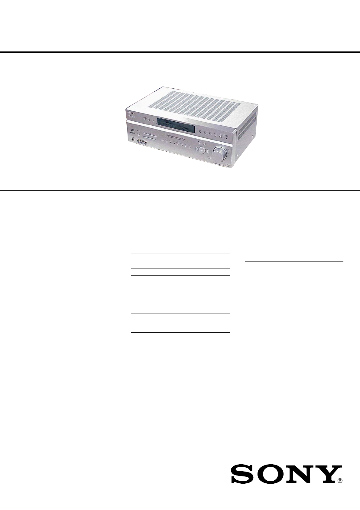
STR-K1000P
Amplifier section
Power Output
1)
Models of area code SP, MX, E51
(6 ohms 1 kHz, THD 0.7%)
FRONT
2)
: 80 W/ch
CENTER
2)
: 80 W
SURR
2)
: 80 W/ch
SURR BACK
2)
: 80 W
(6 ohms 1 kHz, THD 10%)
FRONT
2)
: 130 W/ch
CENTER
2)
: 130 W
SURR
2)
: 130 W/ch
SURR BACK
2)
: 130 W
Models of area code AUS
(6 ohms 120 Hz – 20 kHz, THD 0.09%)
FRONT
2)
: 70 W/ch
CENTER
2)
: 70 W
SURR
2)
: 70 W/ch
SURR BACK
2)
: 70 W
(6 ohms 1 kHz, THD 0.7%)
FRONT
2)
: 80 W/ch
CENTER
2)
: 80 W
SURR
2)
: 80 W/ch
SURR BACK
2)
: 80 W
(6 ohms 1 kHz, THD 10%)
FRONT
2)
: 130 W/ch
CENTER
2)
: 130 W
SURR
2)
: 130 W/ch
SURR BACK
2)
: 130 W
1) Measured under the following conditions:
2) Depending on the sound field settings and the
source, there may be no sound output.
Inputs (Analog)
Area code Power requirements
SP 230 V AC, 50 Hz
AUS, E51 240 V AC, 50 Hz
MX 127 V AC, 60 Hz
MULTI CH IN,
SA-CD/CD, MD/TAPE,
DVD, VIDEO 1, 2, 3
Sensitivity: 800 mV
Impedance: 50 k ohms
Inputs (Digital)
Outputs (Analog)
Reproduction frequency range:
28 – 20,000 Hz
Tone
DVD (Coaxial) Sensitivity: –
Impedance: 75 ohms
VIDEO 2, SA-CD/CD
(Optical)
Sensitivity: –
Impedance: –
MD/TAPE (OUT),
VIDEO 1 (AUDIO OUT)
Voltage: 800 mV
Impedance: 10 k ohms
SUB WOOFER Voltage: 2 V
Impedance: 1 k ohm
Gain levels ±6 dB, 1 dB step
FM tuner section
Tuning range 87.5 - 108.0 MHz
Antenna FM wire antenna
Antenna terminals 75 ohms, unbalanced
Intermediate frequency 10.7 MHz
AM tuner sectio n
Tuning range
Models of area code SP, AUS
With 9-kHz tuning scale: 531 – 1,602 kHz
Models of area code E51
With 10-kHz tuning scale: 530 – 1,610 kHz
3)
With 9-kHz tuning scale: 531 – 1,602 kHz
3)
Models of area code MX
With 10-kHz tuning scale: 530 – 1,610 kHz
Antenna Loop antenna
Intermediate frequency 450 kHz
3) You can change the AM tuning scale to 9 kHz or 10
kHz. After tuning in any AM station, turn off the
receiver. While holding down PRESET TUNING +
or TUNING +, press ?/1. All preset stations will be
erased when you change the tuning scale. To reset
the scale to 10 kHz (or 9 kHz), repeat the procedure.
SERVICE MANUAL
Ver. 1.0 2005.04
• STR-K1000P is the tuner and the amplifier
section in HT-DDW1000.
Manufactured under license from Dolby Laboratories.
“Dolby”, “Pro Logic” and the double-D symbol are trademarks of
Dolby Laboratories.
“DTS” and “DTS Digital Surround” are registered trademarks of
Digital Theater Systems, Inc.
SPECIFICATIONS
E Model
Australian Model
9-879-636-01
2005D1678-1
© 2005.04
Sony Corporation
Audio Group
Published by Sony Engineering Corporation
FM STEREO FM-AM RECEIVER
– Continued on next page –
Page 2

STR-K1000P
Video section
Inputs/Outputs
Video: 1 Vp-p, 75 ohms
COMPONENT VIDEO: Y: 1 Vp-p, 75 ohms
General
Power requirements
Area code Power requirements
SP 220–230 V AC, 50/60 Hz
AUS 240 V AC, 50 Hz
MX 127 V AC, 60 Hz
E51 120/220/240 V AC,
Power consumption 200 W
Power consumption (during standby mode)
Dimensions (w/h/d) (Approx.)
Mass (Approx.) 8.0 kg (17 lb 11 oz)
• Abbrevia tion
AUS : Australian model
E51 : Chilean and Peruvian models
MX : Mexican model
SP : Singapore model
P
B/CB
/B-Y: 0.7 Vp-p,
75 ohms
P
R/CR
/R-Y: 0.7 Vp-p,
75 ohms
80 MHz HD Pass Through
50/60 Hz
0.2 W
430 1 58 310 mm
(16 7/8 × 6 2/8 × 12 2/8
inches) including
projecting parts and
controls
Notes on chip component replacement
• Never reuse a disconnected chip component.
• Notice that the minus side of a tantalum capacitor may be
damaged by heat.
UNLEADED SOLDER
Boards requiring use of unleaded solder are printed with the leadfree mark (LF) indicating the solder contains no lead.
(Caution: Some printed circuit boards may not come printed with
the lead free mark due to their particular size)
: LEAD FREE MARK
Unleaded solder has the following characteristics.
• Unleaded solder melts at a temperature about 40 °C higher
than ordinary solder.
Ordinary soldering irons can be used but the iron tip has to be
applied to the solder joint for a slightly longer time.
Soldering irons using a temperature regulator should be set to
about 350 °C.
Caution: The printed pattern (copper foil) may peel away if
the heated tip is applied for too long, so be careful!
• Strong viscosity
Unleaded solder is more viscou-s (sticky, less prone to flow)
than ordinary solder so use caution not to let solder bridges
occur such as on IC pins, etc.
• Usable with ordinary solder
It is best to use only unleaded solder but unleaded solder may
also be added to ordinary solder.
Design and specifications are subject to change
without notice
SAFETY-RELATED COMPONENT WARNING!!
COMPONENTS IDENTIFIED BY MARK 0 OR DOTTED LINE
WITH MARK 0 ON THE SCHEMATIC DIAGRAMS AND IN
THE PARTS LIST ARE CRITICAL TO SAFE OPERATION.
REPLACE THESE COMPONENTS WITH SONY PARTS WHOSE
PART NUMBERS APPEAR AS SHOWN IN THIS MANUAL OR
IN SUPPLEMENTS PUBLISHED BY SONY.
2
Page 3
STR-K1000P
TABLE OF CONTENTS
1. GENERAL ................................................................... 4
2. TEST MODE ............................................................... 10
3. DIAGRAMS
3-1. Block Diagram – MAIN Section –.................................. 12
3-2. Block Diagram – DISPLAY/POWER Section – ............. 13
3-3. Printed Wiring Board – DIGITAL Board (Side A) –...... 14
3-4. Printed Wiring Board – DIGITAL Board (Side B) –...... 15
3-5. Schematic Diagram – DIGITAL Board (1/4) – .............. 16
3-6. Schematic Diagram – DIGITAL Board (2/4) – .............. 17
3-7. Schematic Diagram – DIGITAL Board (3/4) – .............. 18
3-8. Schematic Diagram – DIGITAL Board (4/4) – .............. 19
3-9. Printed Wiring Board – MAIN Board – ......................... 20
3-10. Schematic Diagram – MAIN Board (1/3) – ................... 21
3-11. Schematic Diagram – MAIN Board (2/3) – ................... 22
3-12. Schematic Diagram – MAIN Board (3/3) – ................... 23
3-13. Printed Wiring Board – STANDBY Section – ............... 24
3-14. Printed Wiring Board – DISPLAY Section – ................. 25
3-15. Schematic Diagram – DISPLAY Section –.................... 26
3-16. Printed Wiring Board
– SPEAKER/HEADPHONE Section –........................... 27
3-17. Schematic Diagram
– SPEAKER/HEADPHONE Section –........................... 28
3-18. Printed Wiring Board – VIDEO IN/OUT Section –....... 29
3-19. Schematic Diagram – VIDEO IN/OUT Section –.......... 30
MODEL IDENTIFICATION
– BACK PANEL –
Parts No.
Model Part No.
E51 model 2-546-121-2[]
SP model 2-546-121-3[]
AUS model 2-546-121-4[]
MX model 2-546-121-5[]
•Abbreviation
AUS: Australian model
E51 : Chilean and Peruvian models
MX : Mexican model
SP : Singapore model
4. EXPLODED VIEWS
4-1. Front Cabinet Section ...................................................... 39
4-2. Chassis Section................................................................ 40
5. ELECTRICAL PARTS LIST .................................. 41
3
Page 4
STR-K1000P
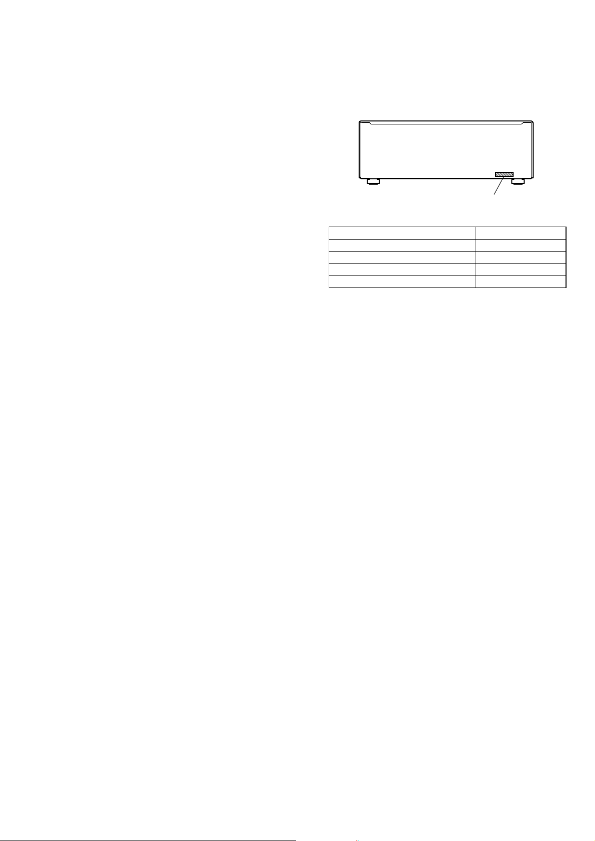
8
Main unit
SECTION 1
GENERAL
This section is extracted
from instruction manual.
ALPHABETICAL ORDER
A - H
A.F.D. (button/indicator) qa (28,
30)
AM wa (21, 22, 23, 38)
DIMMER 4 (24)
DISPLAY 3 (24, 51)
Display 7 (25)
DVD wg (21)
ENTER qg (17, 38, 51)
FM ws (21, 22, 23, 38)
FM MODE es (22)
I - O
Input buttons w; (21, 33, 37, 38,
51)
INPUT MODE qj (33)
IR (receptor) 5 (41, 51)
MAIN MENU 8 (18, 34, 35, 38)
MASTER VOLUME –/+ qh (17,
20, 21, 50)
MD/TAPE wf (21)
MEMORY ef (23)
MOVIE (button/indicator) qs
(29, 30, 50)
MULTI CHANNEL DECODING
(indicator) 6 (22)
MULTI CH IN 9 (22)
MUSIC (button/indicator) qd (30,
50)
P - Z
PHONES (jack) ed (21, 50)
PRESET TUNING –/+ wl (23,
53)
SA-CD/CD wd (21)
SPEAKERS (OFF/A/B/A+B) 2
(15, 39, 50)
SURR BACK DECODING qf
(31)
TUNING –/+ e; (22, 53)
VIDEO 1 wk (21)
VIDEO 2 wj (21)
VIDEO 3 wh (21)
VIDEO 3 IN/PORTABLE AV IN
(jacks) ea (12)
NUMBERS AND SYMBOLS
2CH (button/indicato r) q; (27,
30, 35)
?/1 (power) 1 (17, 35, 53)
</> ql (18, 34, 35, 38)
+/– qk (18, 34, 36, 38)
1
2
6534
7
wawswdwfwgwhwjwk
wle;edesef ea
9q;qaqs qfqd qg
ql
qk
w;
qj
qh
4
Page 5
STR-K1000P
v
V
bB
Before you use your
remote
Inserting batteries into the
remote
Insert R6 ( size-AA) batteries with the + and –
properly oriented in the battery compartment.
When usin g the remote , point it at the remote
sensor on the receiver.
Tip
Under normal conditions, the batteries should last for
about 6 months. Whe n the remote no longer operates
the receiver, replace all batteries with new ones.
Notes
•Do not leave the remote in an extremely hot or humid
place.
•Do not use a new battery wit h an old one.
•Do not expose the remote sensor to direct sunlight or
lighting apparatuses. Doing so may cause a
malfunction.
•If you don’t use the remote for an extended period of
time, remove the batteries to avoid possible damage
from battery leakage and corrosion.
Remote button
description
1
2
3
4
5
6
7
8
9
*
q;
qa
ENTER
*
qs
*
qd
TV ?/1 AV ?/1
RM SET UP
SYSTEM STANDBY
VIDEO1 VIDEO2 VIDEO3 DVD
AV1 AV2
MD/TAPE
SA-CD/CD
2CH
A.F.D.
123
456
AUDIO
ANGLE
789
SUBTITLE ENTER
>
.
0/10 >10/11 12
SHIFT
D.TUNING DISC ALT
Mm
ANT
CLEAR
H
TOP MENU/
GUIDE
V
v
DISPLAY
TV VOL TV CH
RETURN/EXIT
P
TUNER
MOVIE
DUAL
MONO
JUMP/
TIME
-
SEARCH MODE
X
AV MENU
bB
O
TV/
VIDEO
?/1
SLEEP
AUX
MULTI CH
MUSIC
SB
DECODING
PRESET/
CH/D.SKIP
x
MUTING
MASTER
VOL
MAIN
MENU
TEST
TONEWIDE
ef
ed
es
ea
e;
wl
wk
wj
wh
wg
wf
wd
ws
wa
w;
ql
qk
qj
qh
qg
qf
*
*The H, TV VOL +, TV CH + and MASTER
VOL + buttons have a tactile dot. Use the tactile dot
as a reference when operating the receiver and other
audio/video components.
5
Page 6

STR-K1000P
The tables below show the settings of each
button.
Remote
Button
A.F.D. 7 Receiver Selects the decoding
ALT wd Remote When ALT button
ANGLE
7
ANT 9 VCR/
AUDIO
7
AUX e; Receiver To liste n to an audio
AV MENU qaVCR/
AV13 and
AV2 4
AV ?/1edTV/VCR/
Operations Function
mode for audio sound.
lights up, it changes the
remote key function to
activate those buttons
with orange printing.
DVD player/
Blu-ray disc
recorder
Satellite tuner
TV/VCR/
DVD player/
Satellite tuner/
Blu-ray disc
recorder/
Hard disc
recorder/PSX
Satellite tuner/
DVD player/
Blu-ray disc
recorder/
Hard disc
recorder/PSX
Remote Selects the command
CD player/
VCD player/
LD player/
DVD player/
MD deck/
DAT deck/
Blu-ray disc
recorder/
Hard disc
recorder/PSX/
Satellite tuner
Selects viewin g ang le
or changes the angles.
Selects output signal
from the antenna
terminal: TV signal or
VCR program.
Changes the sound to
Multiplex, Bilingual or
Multi channel TV
Sound.
equipment.
Displays menu.
mode of the remote.
Turns the audio and
video components on or
off.
Remote
Button
CLEAR 9 CD player/
DISC ws CD player/
DISPLAY qaTV/VCR/
D.TUNING 9Receiver Enters direct tuning
DUAL
MONO 7
DVD es Receiver To watch DVD.
ENTER wf TV/VCR/
ENTER qa Receiver/
JUMP/TIME 7Satellite tuner/
MAIN
MENU qh
Operations Function
Clears a mistake when
DVD player/
Blu-ray disc
recorder/PSX/
Satellite tuner
VCD player
VCD player/
LD player/
DVD player/
Receiver/
CD player/
MD deck/
Blu-ray disc
recorder/
Hard disc
recorder/PSX/
Satellite tuner
Receiver Selects the language
Satellite tuner/
LD player/MD
deck/DAT
deck/Tape
deck/
Blu-ray disc
recorder/
Hard disc
recorder/PSX
VCR/
Satellite tuner/
DVD player
TV/Blu-ray
disc recorder
CD player/
MD deck/
VCD player/
DVD player
Receiver Selects the menu of
you press the
incorrect numeric
buttons or returns to
continuos playback
etc.
Selects a disc dir ectly
(multi-disc changer
only).
Selects information
displayed on the TV
screen.
mode.
you want during
digital broadcast.
After selecting a
channel, disc or track
using the numeric
buttons, press to enter
the value.
Enters the selection.
Toggles between the
previous and the
current channels.
Shows the time or
displays the playing
time of disc, etc.
the receiver.
6
Page 7

STR-K1000P
Remote
Button
MASTER
VOL +/–
qk
MD/TAPE 5Receiver To listen to Minidisc
MOVIE 7 Receiver Selects the pre-
MULTI CH wkReceiver Selects MULT I CH
MUSIC wj Receiver Selects the pre-
MUTING ql Receiver Mutes the sound from
PRESET/
CH/
D.SKIP +/– wgTV/VCR/
RETURN/
EXIT qa
RM SET UP 2Remote To set up the remote.
SA-CD/CD 6Receiver To listen to Super
SB
DECODING
wh
SEARCH
MODE ws
SHIFT 9 Receiver Selects a memory
Operations Function
Receiver Adjusts the master
volume of the
receiver.
or audio tape.
programmed sound
fields for movie.
IN source.
programmed sound
fields for music.
the receiver.
Receiver Selects pr es et
stations.
Selects preset
Satellite tun er/
Blu-ray disc
recorder/
Hard disc
recorder
CD player/
VCD player/
DVD player/
MD deck/
LD player
VCD player/
LD player/
DVD player
Satellite tuner Exits the menu.
Receiver Selects the surround
DVD player Selects searching
channels.
Skips discs (multi-
disc changer only).
Returns to the
previous menu.
Audio CD or compact
disc.
back decoding modes.
mode. Press to select
the unit for search
(track, index, etc.)
page for presetting
radio stations or
tuning to preset
stations.
Remote
Button
SLEEP ef Receiver Activates the sl eep
SUBTITLE 8DVD player Changes the subtitles.
SYSTEM
STANDBY
(Press AV
?/1 ed and
?/1 ef at
the same
time)
TEST
TONE qg
TOP MENU/ DVD player Displays DVD title.
GUIDE qa Satellite tuner/
TUNER wl Receiver To listen to radio
TV CH +/– qdTV Selects preset TV
TV/VIDEO qjTV Selects input signal:
TV VOL
+/– qs
TV ?/1 1 TV Turns the TV on or
VIDEO1 3 Receiver To watch VCR.
VIDEO2 4 Receiver To watch VCR.
VIDEO3 ea Receiver To watch VCR.
WIDE qf TV Selects the wide
Operations Function
function and the
duration which the
receiver turns off
automatically.
Receiver/
TV/VCR/
Satellite tuner/
CD player/
VCD player/
LD player/
DVD player/
MD deck/
DAT deck
Receiver Ou tputs test tone.
Blu-ray disc
recorder/
Hard disc
recorder/PSX
TV Adjusts the volume of
Turns off the receiv er
and other Sony audio/
video components.
Displays guide menu.
programs.
channels.
TV input or video
input.
the TV.
off.
(VTR mode 3)
(VTR mode 1)
(VTR mode 2)
picture mode.
7
Page 8

STR-K1000P
Remote
Button
1-9 7 and
0/10 8
2CH 7 Receiver Selects 2CH
>10/11 8 CD player/
-/-- ws TV/
?/1 ef Receiver Turns the receiver on
./>8VCR/
Operations Function
Receiver Use with SHIFT to
preset radio station or
tuning to preset
stations and with
D.TUNING for direct
tuning.
CD player/
VCD player/
LD player/
DVD player/
MD deck/
DAT deck/
Tape deck
TV/VCR/
Satellite tuner/
Blu-ray disc
recorder/
Hard disc
recorder/PSX
VCD player/
LD player/
MD deck/
Tape deck/
TV/VCR/
Blu-ray disc
recorder/
Hard disc
recorder/PSX/
Satellite tuner
Blu-ray disc
recorder/
Hard disc
recorder/PSX/
Satellite tuner
CD player/
VCD player/
LD player/
DVD player/
MD deck/
DAT deck/
Tape deck/
Blu-ray disc
recorder/
Hard disc
recorder/PSX
Selects track
numbers.
0/10 selects track 10.
Selects channel
numbers.
STEREO mode.
Selects track numbers
over 10.
Selects the channel
entry mode, ei ther one
or two digit.
or off.
Skips tracks.
Remote
Button
m/M
9
N q; VCR/
X w; VCR/
x wa VCR/
Operations Function
CD player /
VCD player/
DVD player/
LD player/
MD deck/
Blu-ray disc
recorder/
Hard disc
recorder/PSX
VCR/
DAT deck/
Tape deck
CD player /
VCD player/
LD player/
DVD player/
MD deck/
DAT deck/
Tape deck/
Blu-ray disc
recorder/
Hard disc
recorder/PSX
CD player /
VCD player/
LD player/
DVD player/
MD deck/
DAT deck/
Tape deck/
Blu-ray disc
recorder/
Hard disc
recorder/PSX
CD player /
VCD player/
LD player/
DVD player/
MD deck/
DAT deck/
Tape deck/
Blu-ray disc
recorder/
Hard disc
recorder/PSX
Searches tracks i n t he
forward or backward
direction.
Fastforwards or
rewinds.
Starts playback.
Pauses playback or
recording. (Also starts
recording with
components in
recording stan dby. )
Stops playback.
8
Page 9

STR-K1000P
Remote
Button
O qa VCD player/
V/v qa Receiver Selects a menu item.
B/b qa Receiver Adjusts or changes
V/v/B/b qa VCR/
Notes
•The AUX and 12 buttons on the remote are not
available for receiver operation.
•Some func tions explained in this sec tion may not
work depending on the model.
•The above explanation is intended to serve as an
example only. Therefore, depending on the
component the above operation may not be possible
or may operate differently than described.
•When you press input buttons (VIDEO1, VIDEO2,
VIDEO3 or DVD), the input mode of the TV might
not switch to the corresponding input mode that you
want. In this case, press TV/VIDEO button to switch
the input mode of the TV.
•To activate the buttons with orange printin g, pre ss
ALT first before pressing the buttons.
Operations Function
Returns to the
LD player/
DVD player/
Blu-ray disc
recorder/
Hard disc
recorder/PSX/
Satellite tun er
DVD player/
Blu-ray disc
recorder/
Hard disc
recorder/PSX/
Satellite tun er
previous menu or
exits the menu.
the setting.
Selects a menu item.
Selecting the command
mode of the remote
Set the remote command mode using the
RM SET UP button and the remote command
mode buttons.
Selecting the command mode
You can switch the command mod e (AV1 and
AV2) of the remote. If the c ommand mode of the
receiver and the remot e is different, you can no t
use the remote to operate the receiver. To
change the command mode of the recei ver, see
page 51.
Press AV1 (or AV2) while holding down
RM SET UP.
The indicator flashes once (twice for AV2) ,
then the command mode switch es.
To check the command mode of
the remote
Press RM SET UP. You can check the remot e by
the indicator.
Mode Indicator flashes
AV1 once
AV2 twice
To reset the remote to factory
settings
Press ?/1, AV ?/1 and MASTER VOL – at
the same time.
The indicator flashes 3 times, then goes off.
9
Page 10
STR-K1000P
SECTION 2
TEST MODE
FACTORY PRESET MODE
• All preset contents are reset to the default setting.
• Procedure:
While depressing the FM MODE and the DISPLA Y buttons
simultaneously, press the power ?/1 button to turn on the
main power.
The message “FACTORY” appears and the present contents
are reset to the default values.
AM CHANNEL STEP 9 kHz/10 kHz
SELECTION MODE
• Either the 9 kHz step or 10 kHz step can be selected for the
AM channel step.
• Procedure:
Set the FUNCTION to AM. Turn off the main power.
While depressing the TUNING+ button or the PRESET
TUNING+ button, press the power ?/1 button to turn on
the main power. Either the message “9 k STEP” or “10 k
STEP” appears. Select the desired step.
This mode is only for Australian and E models.
FLUORESCENT INDICATOR TUBE TEST MODE
• All fluorescent segments are tested. When this test is activ ated,
all segments turn on at the same time, then each segment turns
on one after another.
• Procedure:
While depressing the TUNING– and the SPEAKERS (OFF/
A/B/A+B) buttons simultaneously, press the power ?/1
button to turn on the main power.
1. All segments turn on.
kHz
mft.
MHz
kHz
mft.
MHz
kHz
mft.
MHz
MEMORY
DIRECT
dB
MEMORY
DIRECT
dB
MEMORY
DIRECT
SP A
D
D
LFE
SW
CR
L
SL S SR
SBL SB SBR
D
SP B SLEEP OPT COAX MULTI CH IN 96/24
D
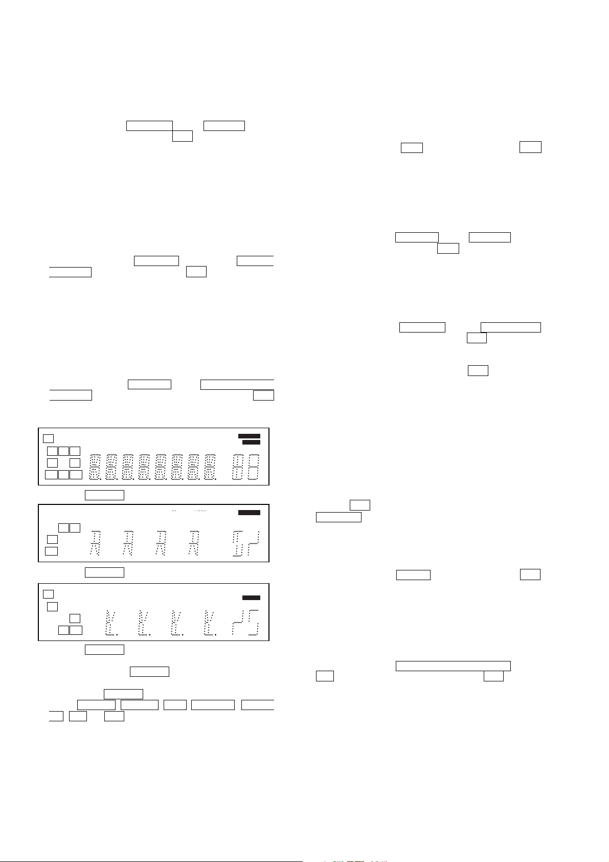
DIGITALEX PRO LOGIC II x DTS-ES NEO:6 MPEG-2 AAC RDS
D.RANGE EQ STEREO MONO
2. Press the VIDEO 1 button, confirm display.
SP A
D
D
LFE
LSWR
S
SB
D
SP B SLEEP OPT COAX MULTI CH IN 96/24
D
DIGITALEX PRO LOGIC II x DTS-ES NEO:6 MPEG-2 AAC RDS
D.RANGE EQ STEREO MONO
3. Press the VIDEO 1 button, confirm display
SP A
D
D
D
DIGITALEX PRO LOGIC II x DTS-ES NEO:6 MPEG-2 AAC RDS
D.RANGE EQ STEREO MONO
C
SL SR
SBL SBR
D
SP B SLEEP OPT COAX MULTI CH IN 96/24
4. Press the VIDEO 1 button, All segments turn off.
5. Every pressing of the VIDEO 1 button turns on each
segment one after another in the same order.
(Not only the VIDEO 1 button, but also the other buttons
such as VIDEO 2 , VIDEO 3 , D VD , MD/TAPE , SA-CD/
CD , FM and AM can be used.)
SOUND FIELD CLEAR MODE
•The preset sound field is cleared when this mode is activated.
Use this mode before returning the product to clients upon
completion of repair.
• Procedure:
While depressing the 2CH button, press the power ?/1
button to turn on the main power.
The message “SF. CLR.” appears and initialization is
performed.
SOFTWARE VERSION DISPLAY MODE
•The software version is displayed.
• Procedure:
While depressing the TUNING– and the DISPLAY buttons
simultaneously, press the power ?/1 button to turn on the
main power. The model name, destination and the software
version are displayed.
KEY CHECK MODE
• Button check
• Procedure:
While depressing the TUNING– and the MAIN MENU
buttons simultaneously , press the power ?/1 button to turn
on the main power.
“REST 30” appears.
Every pressing of any button other than ?/1 counts down
the buttons. The buttons which are already counted once are
not counted again. When all buttons are pressed “REST 00”
appears.
AUTO BETICAL MODE
•This mode is installed in the Europe models only. When this
mode is used, the receiver scans the broadcasts that can be
received by the tuner, and sets up the broadcasts. Be sure to
start scanning after connecting the antenna.
• Procedure:
1. Check that the antenna is connected.
2. Press the ?/1 button to turn on the power while pressing the
MEMORY button.
CHANGE COMMON MODE
•This mode is command mode changed to AV 1 or AV2.
• Procedure:
While depressing the ENTER button, press the power ?/1
button to turn on the main power.
Either the message “C.MODE.AV 1” or “C.MODE.AV 2”
appears.
SHIPMENT MODE
• All preset contents are reset to the default setting.
• Procedure:
While depressing the SPEAKERS (OFF/A/B/A+B) and the
FM buttons simultaneously, press the power ?/1 button to
turn on the main power.
“CLEARED” appears and switch off the set.
10
Page 11
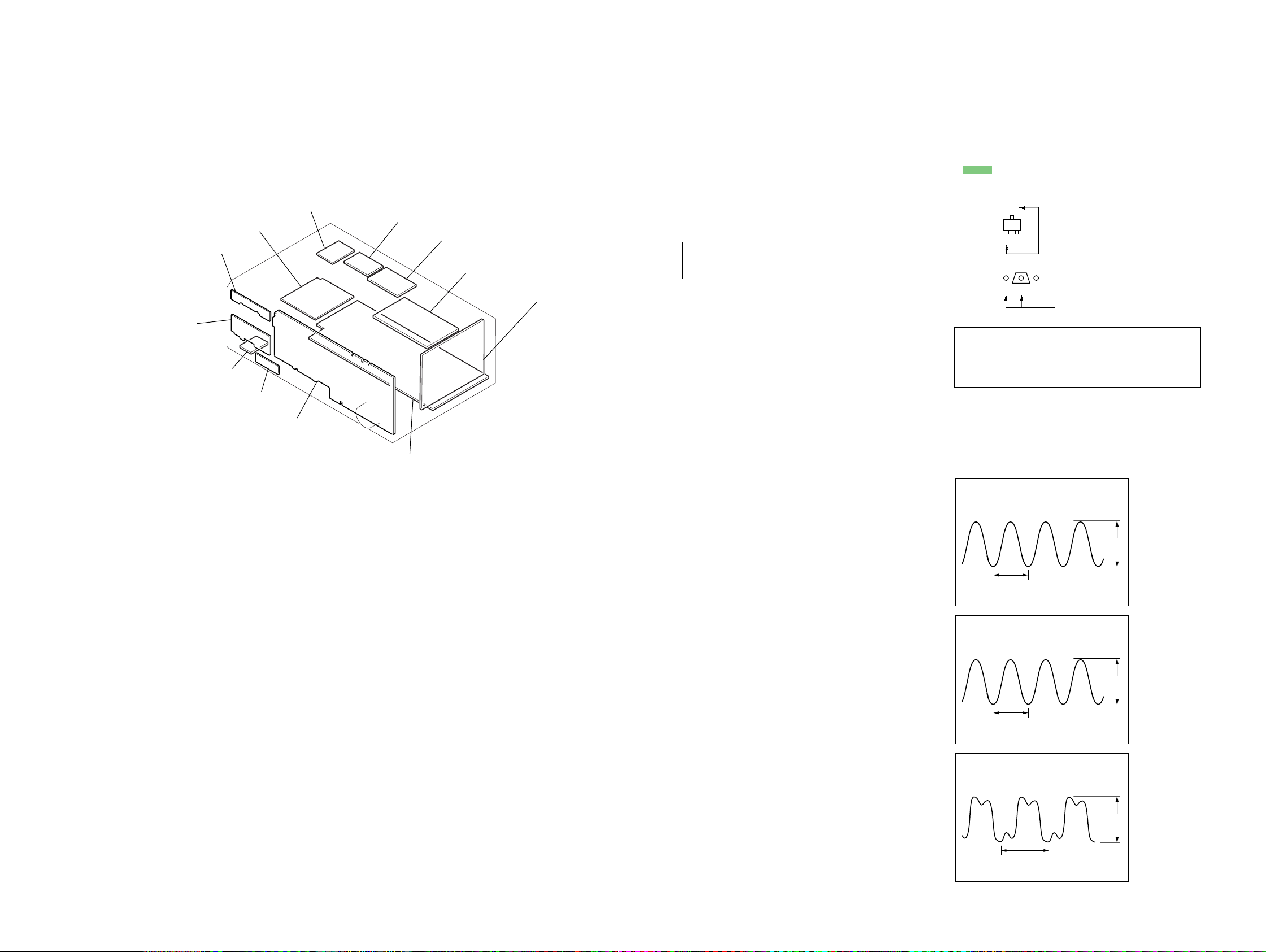
SECTION 3
DIAGRAMS
STR-K1000P
• Circuit Boards Location
POWER board
TUNING board
HEADPHONE board
AC SELECT board
(E51 model only)
STANDBY board
VIDEO3 board
DISPLAY board
SPEAKER B (P) board
SPEAKER C/SB board
VIDEO board
MAIN board
DIGITAL board
THIS NOTE IS COMMON FOR PRINTED WIRING BOARDS AND SCHEMATIC DIAGRAMS.
(In addition to this, the necessary note is printed in each block.)
For Schematic Diagrams.
Note:
• All capacitors are in µF unless otherwise noted. (p: pF)
50 WV or less are not indicated except f or electrolytics and
tantalums.
• All resistors are in Ω and 1/
specified.
• % : indicates tolerance.
• f : internal component.
• 2 : nonflammable resistor.
• 5 : fusible resistor.
• C : panel designation.
Note: The components identified by mark 0 or dotted
line with mark 0 are critical for safety.
Replace only with part number specified.
• A : B+ Line.
• B : B+ Line.
•Voltages and wavef orms are dc with respect to ground under no-signal (detuned) conditions.
No mark : FM
•Voltages are taken with a VOM (Input impedance 10 MΩ).
Voltage variations may be noted due to normal production
tolerances.
•Waveforms are taken with a oscilloscope.
• Circled numbers refer to waveforms.
• Signal path.
F : FM
J : ANALOG
c : DIGITAL
I : VIDEO
•Abbreviation
AUS: Australian model
E51 : Chilean and Peruvian models
MX : Mexican model
SP : Singapore models
4
W or less unless otherwise
For Printed Wiring Boards.
Note:
• X : parts extracted from the component side.
• a: Through hole.
• f : internal component.
• : Pattern from the side which enables seeing.
• Indication of transistor.
C
Q
B
E
B
Caution:
Pattern face side: Parts on the pattern face side seen from
(Side A) the pattern face are indicated.
Parts face side: Parts on the parts face side seen from
(Side B) the parts face are indicated.
These are omitted.
CE
These are omitted.
•Waveforms
– DIGITAL Board –
1
IC1501 9 (MCLK1)
72 ns
1 V/DIV, 40 ns/DIV
2
IC1101 id (X1)
41.6
µ
1 V/DIV, 20 ns/DIV
3
IC1301 ws (XIN)
81 ns
1 V/DIV, 40 ns/DIV
3.4 Vp-p
4.2 Vp-p
s
4.4 Vp-p
STR-K1000P
1111
Page 12
STR-K1000P
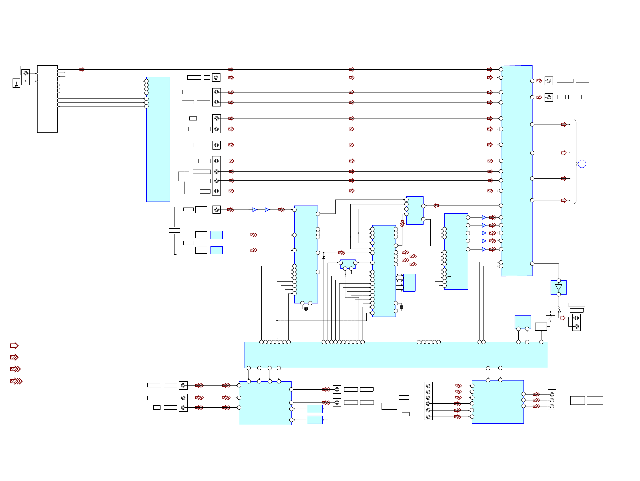
3-1. BLOCK DIAGRAM – MAIN SECTION –
TN1
FM
75 Ω
COAXIAL
AM
TUNER PACK
FM
AM
R CH
ST-DO
ST-DI
STEREO
TUNED
MUTING
L CH
CLK
CE
• R-CH is omitted due to same as L-CH.
• Signal Path
: FM
: ANALOG
: DIGITAL
: VIDEO
R-CH
TUNER +10V10V
IC1101(1/3)
SYSTEM CONTROL.
73
DO
17
TUNER-DATA
16
T.SERIAL CLK
74
SLATCH
76
STEREO
75
TUNED
78
MUTE
VIDEO 1
DIGITAL
J201
(1/2)
VIDEO IN
J200
(1/2)
VIDEO INVIDEO 2
VIDEO INDVD
MULTI
VIDEO 1
VIDEO 2
CH
IN
COAXIAL
OPTICAL
SA-CD/CD
DVD
MD/TAPE
J402
J404 (1/2)
AUDIO IN
AUDIO IN
J403 (1/2)
AUDIO INVIDEO 3
CENTER
SUB WOOFER
SURROUND
FRONT
DVD
IN
VIDEO 2
IN
SA-CD/
CD IN
J298
J401
IC401
ANALOG SOUND
PROCESSOR
38
INIR
IN
IN
IC1401
J1301
IC1351
OPTICAL
IN
IC1354
OPTICAL
IN
IC1301
DIGITAL AUDIO
93
XMODE
VCC
VEE
CKSEL1
1
15
16
14
5
3
4
35
36
38
37
34
17
48
47
I/F RECEIVER
DIN2
DIN0
DINI
DO
DI
CLK
CE
ERROR
XSTATE
XMODE
CKSEL1
XIN XOUT
22 21
X1301
12.288MHz
XMCK
CK OUT
LRCK
DATAO
AUDIO
+5V REG
-5V REG
BCK
IC807
IC804
20
IC1501
AUDIO DSP
22
13
14
15
16
D1101
24
92
DATA0
2
GP9
BST SEL
+ V
- V
18
HD OUT
IC1503
SELECTOR
6
SB
AY
1 5
20
19
HCLK
HD IN
VIDEO OUT
VIDEO OUT
2
4
5
7PM3
6
BST
HCS
XRST
HACN
J201
(2/2)
MONITOR
J200
(2/2)
VIDEO 1
SCK OUT
KFSI0
29
BCKO
BCKI2
28
LRCKI2
17
BCKII
15
LRCKII
SDO1
60
SDI2
SDO2
SDO3
19
LRCK0
SDO4
69
GP8
68
GP9
35
HD OUT
33
HD IN
34
HCLK
36
HCS
32
HACN
PM
113
56
MCLK1
BST
2
XRST
MCLK2
59
EXLOCK
COMPONENT
VIDEO
IC1303
IC1303
35
62
98 97 95 96 99 100 94 1
DI
CE
DO
CLK
ERROR
XSTATE
SW4
89
6
13
V1
SW4
5
V2
3
DVD
86
14
SW1 SW1
IC203
VIDEO AMP
SW3
88
87
4
10
SW3
SW2 SW2
M.OUT
V.OUT
14
20
19LRCKO
18SDI1
23
24
25
26
9
13.9MHz
12
IC1101(2/3)
SYSTEM CONTROL
VIDEO 2
DVD
16
13
14
15
IC1502
SRAM
X1502
SYSCLK
LRCK
BCK
DOUT
P
P
P
P
AD CONVERTER
LIN
1
RST
6
10
9
12MC13MC14
RST(800)
RST(680)
J301
(1/2)
Y
B/CB
/B-Y
R/CR
/R-Y
Y
B/CB
/B-Y
R/CR
/R-Y
IC1452
AUDIO CODEC
VOUT5
VOUT1
38
MCLKI
40
VOUT3
BCK
41
LRCK
VOUT4
VOUT7
47
DATA3
45
DATA1
46
DATA2
DATA4
31
37
RST
36
ML
35
MC
34
MDI
33
MDO
15
MDI
MDO
IC1403
31
10
IC1405
57
14
IC1404
31
12
IC1404
57
11
IC1406
57
16
27
28
VOL DATA LATCH
3
CH1 IN2
9
CH2 IN2
14
CH3 IN2
5
CH1 IN3
11
CH2 IN3
12
CH3 IN3
VOL_CLK
COMPO SW1
71
2
SW1
IC304
VIDEO AMP
34
INGL
24
INBL
26
INCL
30
INEL
32
INFL
28
INDL
12
INDL
17
INDL
13
INDL
10
INDL
41
AOUTL
49
INCL
52
INCSL
51
INCC
56
INCSW
54
INCSB
60
DATA
59
CLK
COMPO SW2
65
4
SW2
BOUTAL
ROUTBL
OUTSBL
OUT SW
IC1131
EEPROM
SDA SCL
5 6
29 30
SDA
CH1 OUT
20
CH2 OUT
CH3 OUT
OUT L
OUT SL
OUTC
22
18
44
46
88
85
86
83
81
Q560
RELAY
DRIVE
70
SCL
SW RY
RY560
J404
(2/2)
AUDIO OUT
J402
(2/2)
OUT
5
7
J301
(2/2)
Y
P
B/CB
P
R/CR
WOOFER AMP
/B-Y
/R-Y
VIDEO 1
MD/TAPE
L
SL
SL
C
SBL
IC402
J309
SUB WOOFER
AUDIO OUT
MONITOR
OUT
A
DISPLAY
/POWER
SECTION
CONPONENT
VIDEO
STR-K1000P
1212
Page 13
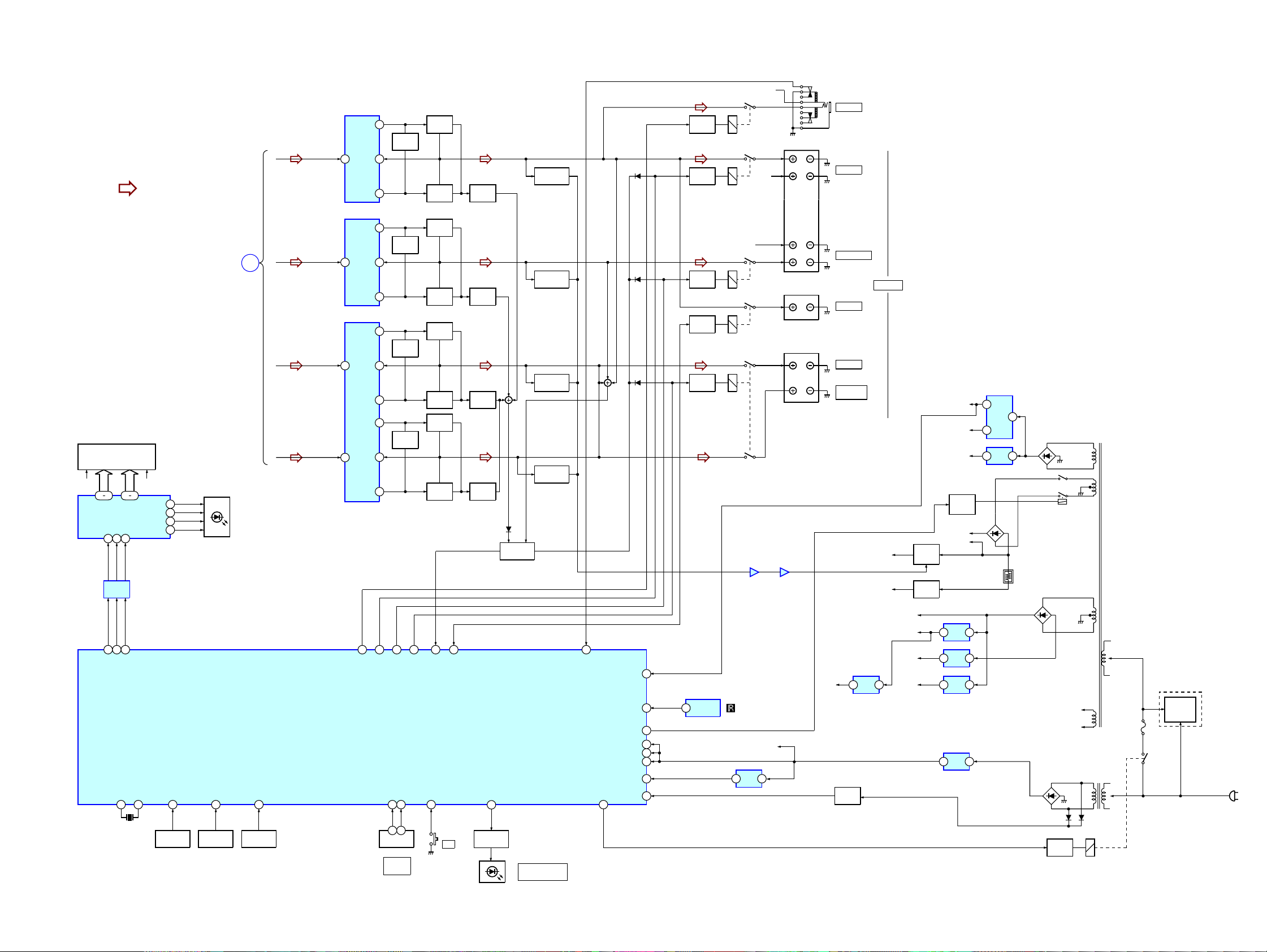
3-2. BLOCK DIAGRAM – DISPLAY/POWER SECTION –
STR-K1000P
• R-CH is omitted due to same as L-CH.
• Signal Path
FL101
FLUORESCENT
INDICATOR TUBE
F1 F2
14 29
42 31
SEG1-16
GRID1-12
DIN8CLK9STB
7
IC101
BUFFER
59
60
57
FL_LAT
FL_CLK
FL_DATA
X1
X0
82 83
X1101
24MHz
: FM
IC100
FL DRIVE
SW1
SW2
SW3
SW4
FUNCTION
S140-143,
S148-153
R-CH
IC701
POWER AMP
+V OUT2
12
Q701,702
LIMITER
L
MAIN
SECTION
A/D0
D101-104
A/D1
39
FUNCTION
KEY
S100-108,
S110
1
2
3
4
38
KEY
A
A/D2
40
FUNCTION
KEY
S120-125,
S128-130
SLSL
C
SBL
8
NF2
IN2
-V OUT2
IC601
POWER AMP
+V OUT2
NF2
IN2
8
-V OUT2
POWER AMP
IC501
+V OUT2
8
NF2
IN2
+V OUT1
NF1
6
IN1
62
HP RY
SYSTEM CONTROL
IC1101(3/3)
9
11
12
9
11
12
9
11-V OUT2
2
5
3-V OUT1
66
FRONT RY
Q651,652
LIMITER
Q501,502
LIMITER
Q571,572
LIMITER
69
REAR RY
VOL_ENC(B)46VOL_ENC(A)
45
3 1
ENCODER
RV102
MASTER
VOLUME
68
C/SB RY
Q703
BOOSTER
Q704
BOOSTER
Q653
BOOSTER
Q654
BOOSTER
Q503
BOOSTER
Q504
BOOSTER
Q533
BOOSTER
Q534
BOOSTER
61
PROTECTOR
POWER KEY
56
S131
?/1
67
SP_B_RY
Q705,706
CURRENT
DETECT
Q655,656
CURRENT
DETECT
Q505,506
CURRENT
DETECT
Q535,536
CURRENT
DETECT
LED DRIVE
47
Q110
D721
Q722,723,725
BLUE LED
PROTECT
SWITCH
D105
MUMLTI CHANNEL
AF POWER
PROTECT
AF POWER
PROTECT
AF POWER
PROTECT
AF POWER
PROTECT
DECODING
Q740
Q640
Q540
Q580
55
HP DETECT
FUSE DETECT
BRIGEABLE RY
POWER RY
58
D731
D733
D734
SIRCS
AVCC
VCC3
VCC5
RSTX
STOP
63
54
72
35
84
23
77
48
1
Q790
RELAY
DRIVE
Q710
RELAY
DRIVE
Q610
RELAY
DRIVE
Q810
RELAY
DRIVE
Q550
RELAY
DRIVE
IC102
REMOTE
CONTROL
RECEIVER
RY791
RY701
RY601
RY610
RY501
R-CH
IC691
21
+3.3V(STBY)
IC1111
RESET
1 2
R-CH
TM601
L
R
SR
SL
TM610
TM501
C
SB
IC691
57
AUDIO
+5V
J791
PHONES
FRONT A
SURROUND
FRONT B
CENTER
SURROUND
BACK
3 1
Q921
AC DET
POWER AMP
IC1001
+5V
REG
SPEAKERS
-B
FL101
-20V
RELAY
+B
AUDIO
+7V
AUDIO
-7V
TUNER
+10V
Q691,692
-B
SWITCH
Q801
-20V REG
+3.3V
+2.5V
+5V
Q809
RELAY
DRIVE
IC801
+7V
1 3
REG
IC802
-7V
3 2
REG
IC1902
+10V
3 1
REG
IC1904
+3.3V
3 1
REG
IC1901
+3.3V
2
REG
4
+2.5V
5
REG
IC1031
+5V
3 1
REG
D802
+B
-B
D920-923
D805-808
D910-913
D914
Q901
RELAY
DRIVE
RY801
F1
F2
D915
RY901
T901
T902
F901
E51
S901
VOLTAGE
SELECTOR
AC
IN
STR-K1000P
1313
Page 14
STR-K1000P
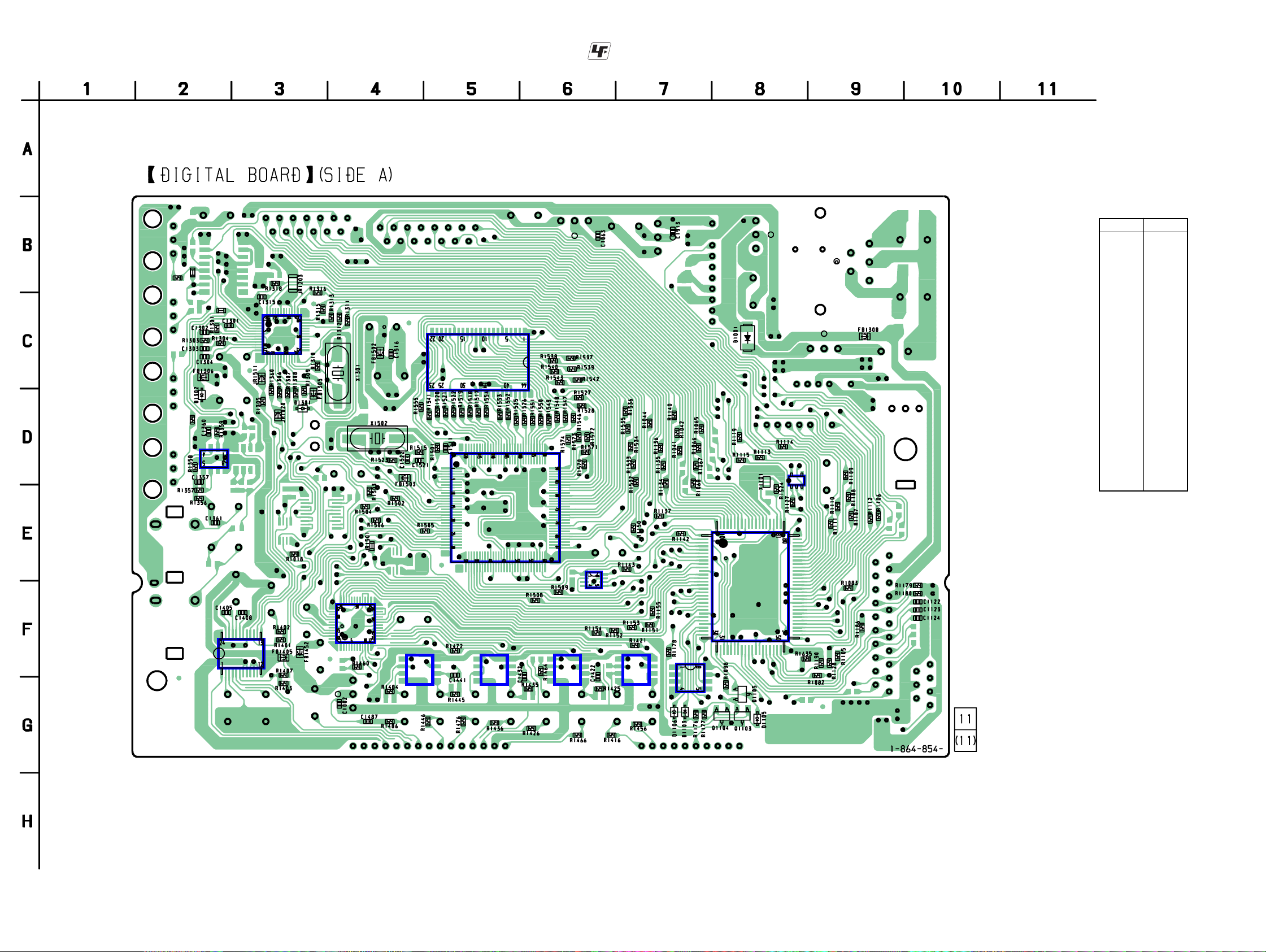
3-3. PRINTED WIRING BOARD – DIGITAL BOARD (SIDE A) –
JR1303
R1351
JR1302
IC1301
R1354
IC1303
• See page 11 for Circuit Boards Location.
IC1502
:Uses unleaded solder.
IC1111
• Semiconductor
Location
Ref. No.
D1001 C-8
D1103 G-7
D1105 G-8
D1106 G-7
D1301 D-3
D1302 D-2
IC1101 F-8
IC1111 D-9
IC1131 G-7
IC1301 C-3
IC1303 D-2
IC1401 F-2
IC1403 F-4
IC1404 F-5
IC1405 F-6
IC1406 G-7
IC1452 F-4
IC1501 E-5
IC1502 C-5
IC1503 F-6
Q1103 G-8
Q1104 G-8
Q1105 G-8
Location
IC1401
IC1452
IC1403
5
8
IC1501
IC1101
IC1503
4
1
IC1404 IC1405
5
8
4
1
5
8
4
1
IC1406
5
8
4
IC1131
1
STR-K1000P
1414
Page 15
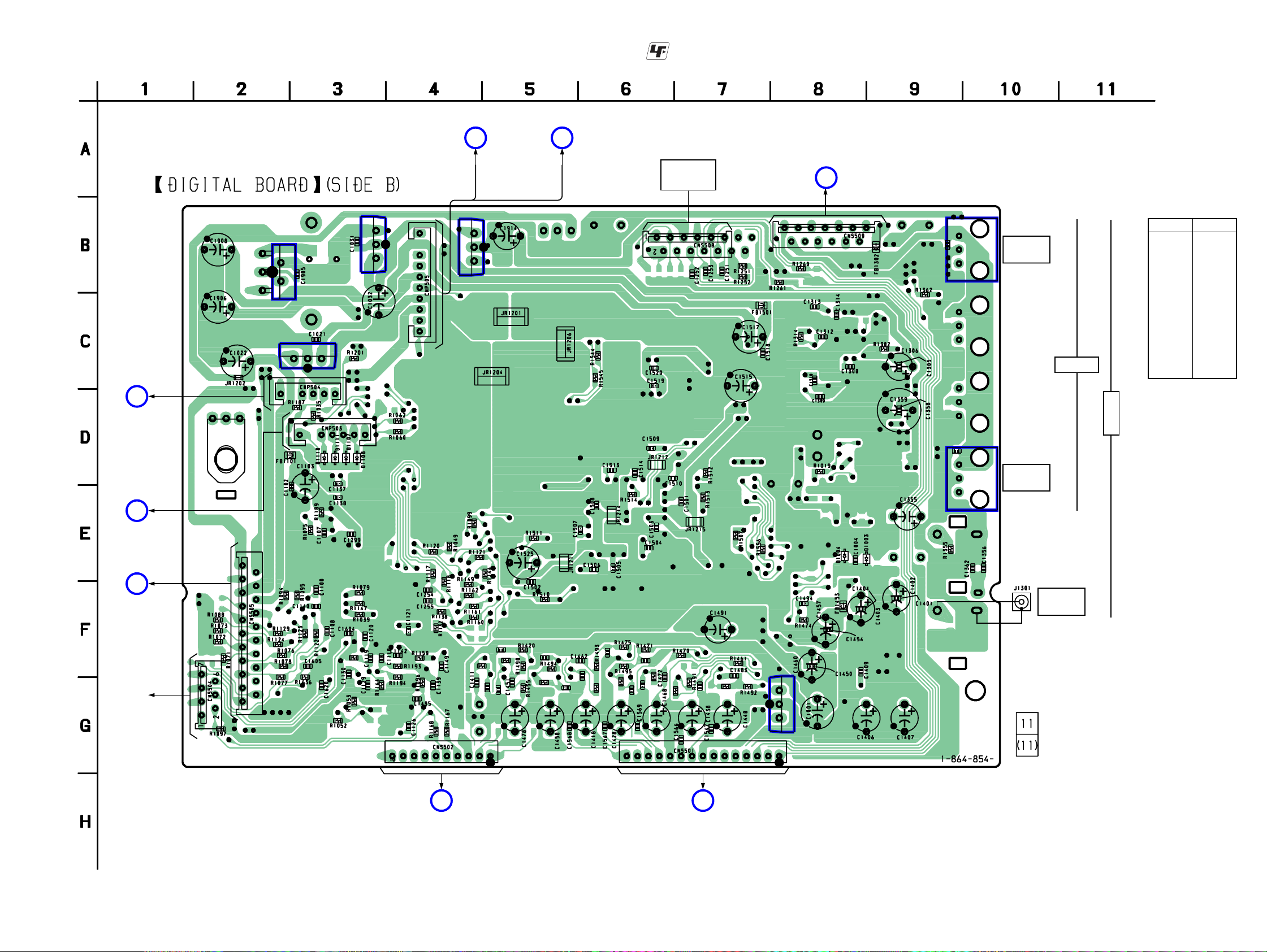
STR-K1000P
3-4. PRINTED WIRING BOARD – DIGITAL BOARD (SIDE B) –
IC1901
IC1031
IC1031
IC1904
• See page 11 for Circuit Boards Location.
STANDBY BOARD
CNP903
(Page 24)
N
Pin No.1 to Pin No.5
MAIN BOARD
CNP912
(Page 20)
K
Pin No.6 to Pin No.9
IC1902
:Uses unleaded solder.
TN1
TUNER UNIT
VIDEO BOARD
CNS250
D
(Page 29)
• Semiconductor
IC1351
1
C1351
VIDEO 2
IN
OPTICAL
Location
Ref. No.
D1003 E-9
D1004 E-8
D1107 D-3
D1108 D-3
D1110 D-3
D1111 D-3
IC1001 F-8
IC1031 B-3
IC1351 B-10
IC1354 D-10
IC1901 B-2
IC1902 B-4
IC1904 C-2
Location
L
MAIN BOARD
CNP911
(Page 20)
M
MAIN BOARD
CNP911
(Page 20)
A
DISPLAY BOARD
CNS100
(Page 25)
FOR
FLASH
PROGRAMMING
DIGITAL
IC1354
C1354
SA-CD /
CD IN
21
20
DVD IN
COAXIAL
R1414
C1413
C1540
R1454
C1453
R1163
2
1
C1544
R1424
C1423
C1463
R1463
C1543
R1434
C1433
C1545
C1473
R1473
R1444
IC1001
R1483
C1442
STR-K1000P
J
MAIN BOARD
CNP500
(Page 20)
MAIN BOARD
I
1515
CNP501
(Page 20)
Page 16
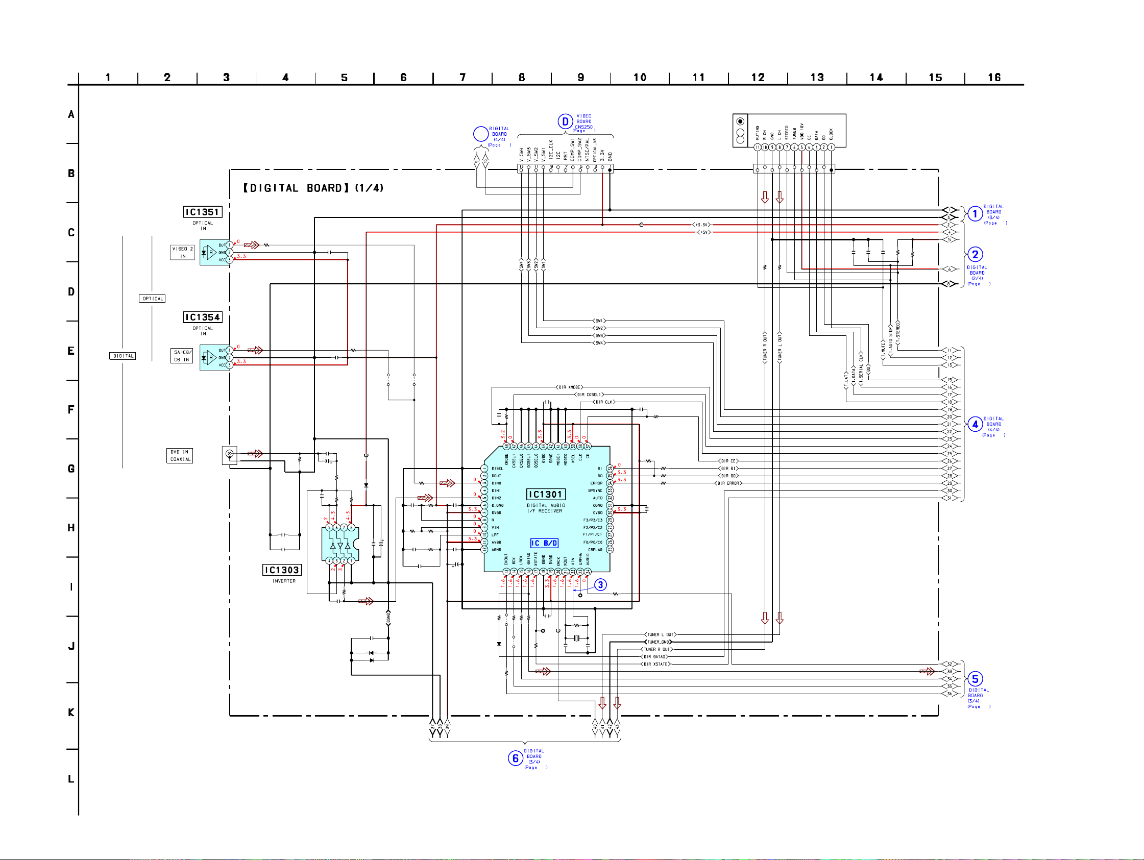
STR-K1000P
3-5. SCHEMATIC DIAGRAM – DIGITAL BOARD (1/4) –
IC1351
TORX141L
IC1354
TORX141L
R1351
100
• See page 11 for Waveform. • See page 31 for IC Block Diagram.
3
19
0.1
C1351
R1354
100
0.1
C1354
TN1
TUNER UNIT
30
CNS508
11P
CN509
13P
FB1302
0
1k
R1261
1k
R1260
C1252 C1253 C1251
0.1 0.1 0.1
R1252 R1251
39k 39k
18
17
J1301
JR1303JR1302
0
0
C1314
100
R1307
IC1301
LC89056W-E
C1308
0.1
TP1004
100
R1309
0.1
TP1003
0
R1310
1M
FB1305
X1301
12.288MHz
18p
C1310
18p
C1309
0.1
10k
C1315
R1308
R1318
22
0UH
100
100
R1306
R1360
JR1511
0
JR1020
R1305
680
1P
R1355
75
C1356
0.01
C1361
C1355
C1357
1p
IC1303
TC7WU04F(TE12R)
0.1
22
25V
C1360
47p
R1356
1k
R1359
100
FB1306
R1358R1357
560k22k
C1004
0.022
D1003
1SS367-T3SONY
D1004
1SS367-T3SONY
0
D1302
1SS355TE-17
0.1
C1358
6.3V
1000
C1359
C1302
0.01
R1303
R1362
100
C1301
0.1
R1301
5.6k
33k
R1302
4.7k
R1304
C1303 C1305C1362
100
0.1 0.10.1
C1304
0.01
C1306
47
16V
D1301
1SS355TE-17
R1311
C1313
100p
R1316
100
19
R1314
10k
100
R1315
100
R1313
100
R1312
C1312
0.1
100
STR-K1000P
18
18
1616
Page 17
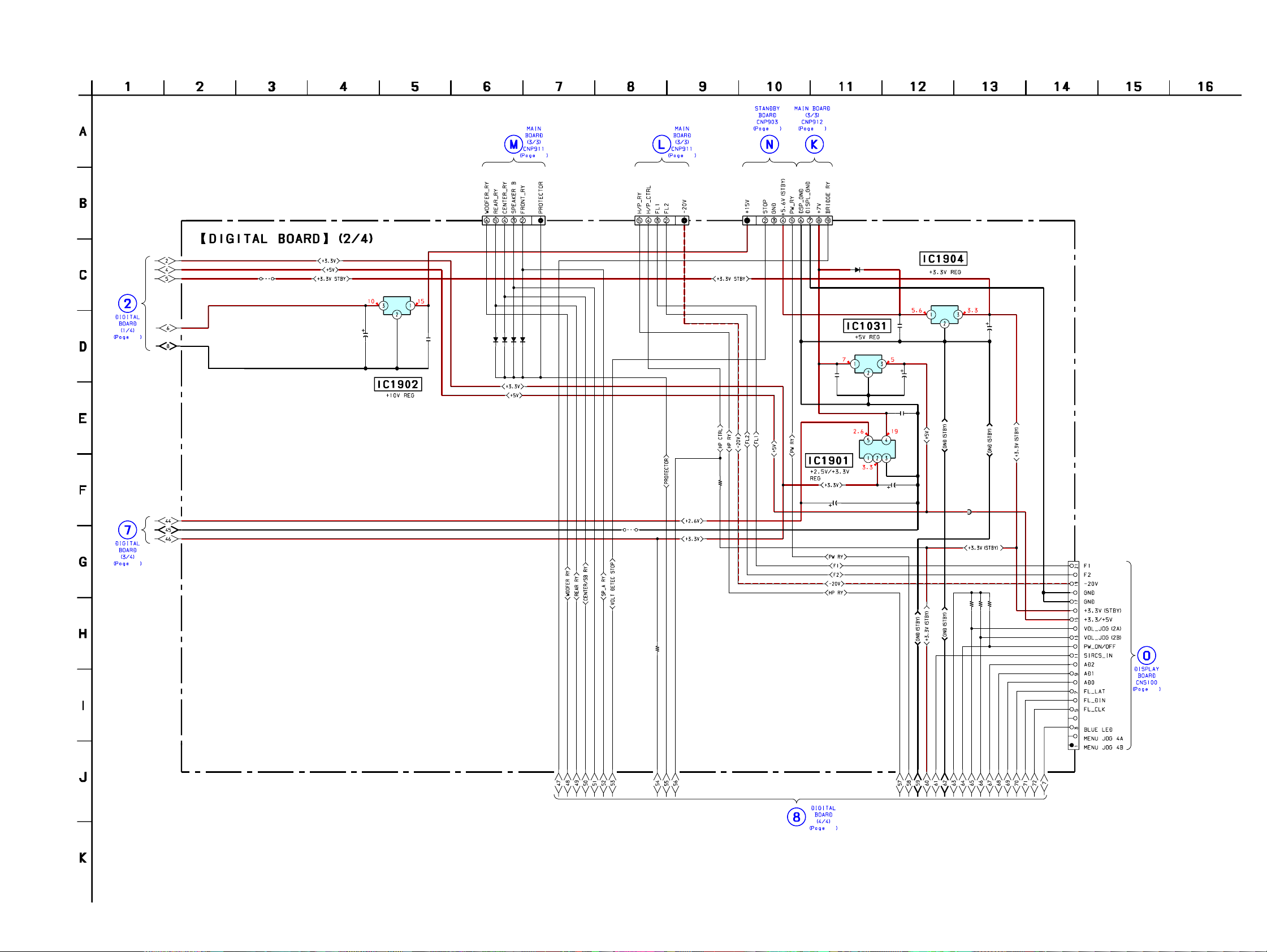
3-6. SCHEMATIC DIAGRAM – DIGITAL BOARD (2/4) –
STR-K1000P
23
23
CNP503
6P
JR1202
0
16
C1914
16V
IC1902
TA7809LS
47
C1913
0.1
25V
1SS355TE-17
1SS355TE-17
D1108
D1107
1SS355TE-17
1SS355TE-17
D1110
D1111
23
CNP504
5P
23
C1031
0.1
SI-3004KWF
CNP505
9P
1SR154-400TE-25
IC1901
D1001
IC1031
BA50BC0T
C1905
0.1
C1021
0.1
C1032
IC1904
BA33BC0T
C1022
470
10V
470
10V
R1187
10k
C1908
470 10V
JR1201
0
18
22k
1201
R
C1906
470 10V
FB1308
0UH
10k
R1179
10k
R1180
10k
R1088
CNS505
21P
26
STR-K1000P
19
1717
Page 18

STR-K1000P
3-7. SCHEMATIC DIAGRAM – DIGITAL BOARD (3/4) –
16
C1450
0
FB1452
0.1
C1460
10
50V
R1474
10k
C1494
0.1
0
FB1453
C1454
0.1
10 50V
C1457
• See page 11 for Waveform. • See page 32, 33 for IC Block Diagrams.
16
0
IC1452
PCM1609KPTR
R1019
0
R1018
C1491
10 50V
FB1502
0
C1515
470
C1516
0.1
10V
C1517
C1518
0.1
470
10V
FB1501
0
220
220
R1520
R1521
C1509
0.1
100
R1501
C1510
0.1
16
17
C1520
0.1
IC1502
IS61LV6416-10TLT
0.1
C1519
220
R1522
220
220
220
220
220
220
220
220
220
220
220
R1519
R1518
R1553
R1554
220
C1514
R1517
0.1
10k
R1514
220
R1526
R1525
R1547
R1548
R1549
R1550
R1551
220
R1546
R1552
0.1
C1513
220
220
220
R1528
R1527
R1545
220
220
220
220
220
R1544
R1543
220
220
220
R1540
R1538
R1539
R1537
R1541
R1542
220
220
220
220
220
220
R1555
R1536
R1535
R1534
R1533
R1532
R1402 IC1401
2.2k PCM1800E/2K
R1401
1k
C1404
0.1
C1403
10 50V
C1408
470p
C1405
470p
C1402
47 16V
C1401
0.1
FB1405
0
1k
C1511
0.1
R1512
C1521
X1502
13.9MHz
C1522
27p
27p
R1523
R1515
220
1M
100
R1502
R1503
100
R1504
100
R1505
220
100
R1506
0
0
0.1
0.1
6.8K
0.1
0.1
8.2k
R1472
R1471
R1461
R1475
R1460
6.8k
R1403
10k
0.1
R1407
100
C1409
C1406
4.7 50V
C1407
4.7
50V
R1492
R1420
R1421
R1470
JR1501
10K
10K
10K
10K
C1544
C1545
C1543
C1540
6.8k
6.8k
6.8k
6.8k
6.8k
R1491
R1494
R1493
R1495
R1490
100
R1507
0
C1501
0.1
TP1018
C1503
R1513
TP1005
10k
IC1501
CXD9718BQ
C1506
0.1
0.1
C1505
TP1012
TP1015
FB1503
C1504
0.1
0UH
100
100
R1556
100
TP1008
TP1010
TP1009
TP1011
R1509
R1508
0.1
C1525
470 10 V
R1574
10k
R1573
10k
R1572
10k
R1571
10k
R1570
10k
C1508
0.1
C1507
0.1
R1511
100
25V
0.1
C1502
R1510
100
R1149
100
IC1503
TC7WH157FU (TE12R)
19
STR-K1000P
CNS501
15P
21
1818
Page 19

STR-K1000P
3-8. SCHEMATIC DIAGRAM – DIGITAL BOARD (4/4) –
16
• See page 11 for Waveform. • See page 31 for IC Block Diagram. • See page 36 for IC Pin Function Description.
16 17
IC1111
S-80929CNMC
-G8ZT2G
C1137
1k
100
R1119
R1113
100
2.2k
2.2k
2.2k
R1115
R1114
R1111
R1061
R1062
100
100
10k
R1147
X1101
24MHz
100
100
100
100
100
100
100
100
100
100
R1044
R1135
R1136
R1140
R1134
100
R1150
100
R1041
R1067
R1042
R1068
R1066
R1065
R1049
R1142
100
R1151
R1152
R1153
R1154
R1161
100
R1160
100
R1121
100
R1155
R1524
0
C1299
0.1
R1120
10k
100
100
100
100
100
1k
R1137
100
R1099
10k
R1162
100
R1144
100
R1143
100
R1110
0.01
C1107
0.1
R1127
100
R1189
2.2k
2.2k
2.2k
R1108
R1109
R1107
R1128
10k
C1108
0.1
100
R1190
10k
IC1101
MB90488
BPF-G-144E1
C1121
0.1
R1112
100
R1039
10k
C1140
0.1
C1138
0.1
100
R1094
10k
R1124
10k
C1100
0.1
R1083
R1095
100
100
R1122
R1123
10k
10k
220p
220p
R1138
R1132
C1255
C1254
10k
R1076
100
R1129
100
16V
0.1
47
C1102
C1103
C1120
0.01
R1194
C1142
0.1
1k
R1118
C1122
0.1
10k
220p
220p
R1096
C1149
C1495
0
FB1101
100
R1106
R1035
2.2k
0.1
2.2k
R1636
C1605
C1604
C1118
1k
R1117
2.2k
0.1
C1620
R1635
0.1
R1105
10k
R1186
10k
C1119
R1164
22K
R1193
0.1
R1163
47k
3.3k
3.3k
3.3k
R1072
R1073
R1071
10k
10k
R1053
R1052
0.01
0.01
C1129
C1130
R1082
100
100
100
R1078
R1077
EXCEPT SP
0.1
R1097
100k
R1159
3.3k
0.1
0.1
C1124
C1123
C1139
0.1
IC1131
BR24L16F-WE2
CNS504
7P
STR-K1000P
D1103
R1178
1SS355TE-17
10k
18
R1177
10k
R1176
10k
C1478
2SC2712-YG-TE85L
C1488
10 50V
10 50V
C1557
0.0022
CNS502
Q1104
R1456
1K
R1416
1k
10P
0.0022
C1487
R1486
0.0022
0.0022
0.0022
1k
R1446
1k
C1566
C1569
C1448
10
C1483 C1441 C1472 C1432 C1422 C1462
50V
680p 680p 0.1 680p 680p 680p
R1484 R1445 R1435 R1464R1425
C1468
00 0 00
10
50V
R1476
10 50V
C1438
1k
R1436
C1428
1k
R1466
C1458
C1418
R1426
1k
10 50V
10 50V
10 50V
1k
C1411 C1451
680p 680p
R1455
0
IC1001
TA7805S
C1001
470
10V
C1002
0.1
C1547
C1568
0.0022
C1567
0.0022
R1168
RT1N141C-TP-1
R1167
R1098
10k
Q1105
2SC2712-YG-TE85L
D1105
1SS355TE-17
D1106
1SS355TE-17
Q1103
100
100
C1126
220p
R1483
6.8k
C1481
330p
NJM4565M(TE2)
R1444
6.8k
IC1403
R1473
8.2k
IC1404
NJM4565M(TE2)
C1442
C1473
330p
0.1
R1434
R1463
6.8k
6.8k
C1433
C1463
330p
330p
R1454
6.8k
6.8k
R1424
C1453C1423
330p
330p
IC1406IC1405
NJM4565M(TE2)NJM4565M(TE2)
6.8k
R1414
C1413
330p
21
1919
Page 20

STR-K1000P
3-9. PRINTED WIRING BOARD – MAIN BOARD –
SA-CD/CD
IN
LR
B
VIDEO3 BOARD
CN201
(Page 29)
SP, AUS
IC401
I
DIGITAL BOARD
CNS501
(Page 15)
• See page 11 for Circuit Boards Location.
MD/TAPE DVD
OUT
IC402
SP, AUS
IN
LR
VIDEO 2 VIDEO 1
AUDIO IN
LR
SP, AUS
AUDIO INRLAUDIO OUT
RL
IC701
:Uses unleaded solder.
VIDEO BOARD
CNP203
C
(Page 29)
FRONT SURROUND
RLLR
SP, AUS
IC801
IC802
RL
SP, AUS
IC601
RL
SP, AUS
SUB
WOOFER
SP, AUS
CENTER
RL
IC691
SUB
WOOFER
AUDIO OUT
G
SP, AUS
SPEAKER B(P)
BOARD
CN610
(Page 27)
FRONT A
R
SURROUND
SP, AUS
IMPEDANCE USE 6-16Ω
R
SP, AUS
SPEAKERS
FRONT A
L
SURROUND
SP, AUS
L
POWER TRANSFORMER
Q
(Page 24)
DIGITAL BOARD
CNP505
K
(Page 15)
STANDBY BOARD
CNP801
P
(Page 24)
SPEAKER C/SB BOARD
CNP502
E
(Page 27)
J
DIGITAL BOARD
CNS502
(Page 15)
IC501
WP02 WP03
F
SPEAKER C/SB BOARD
CNP503
(Page 27)
• Semiconductor Location
Ref. No.
Location
D505 E-4
D540 E-3
D560 B-6
D580 E-1
D585 D-2
D605 E-9
D610 C-6
D640 E-7
D665 E-7
D680 D-8
D690 C-7
D691 C-6
D705 E-5
D710 C-7
D721 D-8
D722 D-8
Ref. No.
D732 D-8
D740 D-4
D750 D-7
D765 E-8
D791 D-10
D801 D-9
D802 C-9
D804 D-9
D805 C-10
D806 C-10
D807 C-10
D808 C-10
D818 B-9
D896 C-5
IC401 C-3
Location
Pin No.6 to Pin No.11 Pin No.1 to Pin No.5
M
DIGITAL BOARD
CNP503
(Page 15)
Ref. No.
IC402 D-3
IC501 D-3
IC601 D-5
IC691 C-6
IC701 D-4
IC801 C-5
IC802 C-5
Q501 E-3
Q502 E-4
Q503 E-4
Q504 E-4
Q505 E-4
Q506 E-4
Q533 E-2
Q534 E-3
Location
L
DIGITAL BOARD
CNP504
(Page 15)
Ref. No.
Location
Q535 E-2
Q536 E-3
Q540 E-3
Q560 C-6
Q571 E-2
Q572 E-3
Q580 E-1
Q601 E-9
Q602 E-9
Q603 E-8
Q604 E-9
Q605 E-9
Q606 E-9
Q610 C-7
Q640 E-6
Q651 E-6
POWER TRANSFORMER
Ref. No.
Location
Q652 E-6
Q653 E-6
Q654 E-6
Q655 E-6
Q656 E-7
Q680 D-8
Q691 D-7
Q701 E-4
Q702 E-5
Q703 E-5
Q704 E-5
Q705 E-5
Q706 E-5
Q710 C-7
Q722 D-8
Q723 D-8
H
R
(Page 24)
HEADPHONE BOARD
CN791
(Page 27)
Ref. No.
Q725 D-8
Q740 E-5
Q750 D-7
Q751 E-7
Q752 E-7
Q753 E-7
Q754 E-8
Q755 E-8
Q756 E-8
Q790 D-9
Q793 D-8
Q795 D-8
Q801 D-9
Q809 C-10
Location
STR-K1000P
2020
Page 21

3-10. SCHEMATIC DIAGRAM – MAIN BOARD (1/3) –
STR-K1000P
WP100
18
10k
R475
10k
R476
CNP500
10P
0.1
C488
0.1
C464
JW401
JW
CNP501
15P
50V
50V
10
10
C762
C702
J402
4P
CC52
R452
*1
1k
R402
CC02
*1
1k
R459
CC59
*1
CC09
*1
CC54
*1
CC04
*1
CC55
*1
CC05
J403
J404
*1
4P
CC07
*1
*1
CC06
*1
CC56
*1
CC08
*1
CC58
*1
6P
R408
R406
R458
R404
1k
R409
R454
1k
R455
R405
R407
R457CC57
R456
1k
C459
1k1k4.7 50V
C409
4.7 50V
1k
1k
1k
1k
1k
1k
1k
C408
4.7 50V
C458
4.7 50V
C403
0.1
C444
2200p
100p
C469
1k
R428
100p
C468
1k
R429
19
C490
C495
10
50V
C485
10
10
50V
50V
IC401
BD3451KS
10 50V
C481
10 50V
C492
10 50V
C493
10 50V
C484
C496
C486
C494
C491
C482
C483
R340
R360C489
R330
R320
R350
R310
R300
JW
JWJW
JW
JW
JW
JW
JW
22
JW
JW
JW
JW
JW
JW
STR-K1000P
MULTI
CH
IN
CENTER
SUB WOOFER
SURROUND
FRONT
CNP503
3P
30
R436
CC36
1k
*2
R435
CC35
1k
*2
CC34
R434
*2
1k
CC33
1k
R433
*2
C445 2200P
CC32
R432
1k
*2
CC31
R431
*2
1k
J404
6P
*2 CC31-CC36
220P:SP,AUS
NO MOUNT:E51,MX
23
2121
Page 22

STR-K1000P
3-11. SCHEMATIC DIAGRAM – MAIN BOARD (2/3) –
IC701
R744
15k
C744
C701
2.2
4.7
R701
100V
1k
50V
68k
C707
100p
C757
100p
C751 R751
4.7
1k
50V
IC601
R743
15k
C651
4.7
R651
50V 1k
C657
100p
C607
100p
R601
C601
1k
4.7
50V
22
IC501
R741
15k
C561 R561
4.7
50V
C501
4.7
50V
R501
1k
D691
ISS133T-72
E2
-TP
R
691
Q
1815G
C
R691
220
2S
R692
220
C743
2.2
100V
C741
2.2
100V
C567
100p
C507
100p
702
R
68k
R752
68k
R652
68k
R602
1k
D690
HZS30-1LTA
R698
10k
R699
470k
C755
33p
500V
R753
2.2k
C753
100
10V 100
C605
33p
500V
R603
2.2k
C603
100
10V
C565
33p
500V
68k
R562
68k
R502
Q692
DTA124ESA-TP
IC691
NJM4565D
R694
10k
C756
100p
C606
100p
C554 C504
R554
• See page 33 for IC Block Diagrams.
47 25V
R732
1
Q571
2SA1115TP-EF
47 25V
C570
2SC3623ATP-LK
C710
47 25V
C760
2SA1115TP-EF
2SA1115-TP-EF
47 25V
C510
Q572
C706
100p
C754
3p
R754
68k
C656
100p
C604
3p
R604
68k
C506
100p
C566
100p
5p 5p
68k
R553 R503
2.2k 2.2k
C553 C503
100
10V
10k47k
R695R696
C691
R690
220k
0.1
C705
33p
500V
C704
3p
R704
R703
68k
2.2k
C703
10V
C655
33p
500V
C654
3p
R654
68k
R653
2.2k
C653
100
10V
C505
33p
500V
C732C733
10
10
100V
100V
68k
R505
100
10V
10k
693
R
R733
1
102
101
P
P
W
W
Q701
2SA1115TP-EF
Q702
2SC3623ATP-LK
2SC3623ATP-LK
47 25V
C660
2SA1115TP-EF
2SA1115TP-EF
47 25V
C610
2SC3623ATP-LK
Q751
Q501
Q502
2SC3623ATP-LK
R792
680 1W
R794
680 1W
R791
2.2k
CC15
*2
RR13
*3
RR14
*3
CC17
*2
1SS133T-72
Q790
2SC1740S-QRT
RY791
D791
R793
82
TM601
CN792
4P
28
CC11
*2
RR11
*3
RR12
*3
CC13
*2
CN807
4P
28
CNP806
4P
28
4.7
C742
0.01
C642
0.01
R677
R623
C752
0.01
R757
C541
0.01
R747
15k
15k
47k
L601
R618
4.7
C681
0.01
R657
15k
15k
R557
15k
1SS133T-72
L701
R718
4.7
1SS133T-72
L651
2SC1815GR-TPE2
D680
1SS133T-72
C680
10
50V
D750
1SS133T-72
C750
10
50V
R773
47k
D540
1SS133T-72
C540
10
50V
D580
1SS133T-72
Q740
2SC1815GR-TPE2
D740
C740
10
50V
D640
C640
10
50V
2SC1815GR-TPE2
Q680
2SC1815GR-TPE2
2SC1815GR-TPE2
C580
10
50V
2SC1815GR-TPE2
RY701
D710
1SS133T-72
.7k
4
R734
745
R
R746
47k
R675
4.7k
R676
47k
Q640
R655
4.7k
R656
47k
L751
R768
4.7
4.7k
R755
R756
47k
Q750
R555
4.7k
R556
47k
Q540
R585
4.7k
R586
47k
Q580
82
E-TP
S
-R
S
795
Q
038
1
SA
2
-TP
E
S
-R
S
725
Q
038
1
A
S
2
1SS133T-72
Q710
2SC1740S-QRT
R731
2.2k
C791
220
10V
C721
220
10V
R780
10k
D722
1SS133T-72
D721
C722
R737
10
39k
50V
R736
1k
R634
82
D610
1SS133T-72
2SC1841TP-PAFAEA
RY601
Q793
2SC1740S-QRT
1SS133T-72
D732
Q723
2SC1740S-QRT
R735
6.8k
Q722
Q610
2SC1740S-QRT
R631
2.2k
Q705
Q706
Q655
C670
220p
R620
4.7k
Q506
C720
220p
R722
1.5k
R725
68k
R638
68k
R672
1.5k
R622
1.5k
R772
1.5k
Q756
2SA1038S-RSE-TP
R520
4.7k
R522
1.5k
Q535
R537
2SA1038S-RSE-TP
C531
0.022
5
60
Q
R624
15k
Q505
10
R534
15k
2SA1038S-RSE-TP
R724
15k
C711
0.022
R717
10
R667
10
C661
0.022
R674
15k
Q656
2SA1038S-RSE-TP
E-TP
S
-R
8S
03
1
2SA
R617
10
R625
68k
R775
68k
C761
0.022
R767
10
R517
10
C511
0.022
R524
15k
D585
1SS133T-72
R523
T-72
05
7
D
C611
0.022
47k
R580
22k
3
S13
1S
1SS133T-72
D605
1SS133T-72
R778
15k
R573
47k
1SS133T-72
R588
15k
R535
68k
R740
22k
R748
15k
R723
47k
R640
22k
R648
15k
D665
R680
22k
R681
15k
R750
22k
R758
15k
D765
1SS133T-72
R540
22k
R546
15k
D505
C581
0.01
R587
15k
R673
47k
R668
R525
68k
C717
47p
82k
R714
2.2k
33
Q703
MN2488
R711
R710
R716
R713
560
C716
R715
47p
Q651
Q601
Q752
R510
2.2k
R660
2.2k
Q602
2SC3623ATP-LK
R574
33
R571R570
82k2.2k
R576
560
R575
33
33
C669
R665
47p
33
R663
560
R666
82k
Q653
MN2488
R661
R664
C666
33
47p
C621
R614
47p
33
2.2k
82k
Q603
MN2488
R610
R611
R613
R616
560
Q604
R615
MP1620
33
C620
47p
C767
R765
47p
33
R763
560
Q754
MP1620
R766
R761R760
82k2.2k
R764
33
C766
47p
C517
47p
R514
33
R511
82k
R516
R513
560
R515
C516
47p
33
C577
47p
Q533
MN2488
R526
Q534
MP1620
C576
47p
Q652
Q704
MP1620
Q654
MP1620
2SA1038S-RSE-TP
R769
4.7k
Q753
MN2488
Q503
MN2488
Q504
MP1620
C539
220p
R531
6.2k
Q536
2SA1038S-RSE-TP
R719
4.7k
R721
6.2k
2SA1038S-RSE-TP
2SA1038S-RSE-TP
R671
6.2k
k
4.7
669
R
p
220
619
C
R621
6.2k
Q606
2SA1038S-RSE-TP
Q755
R771
6.2k
C770
220p
2SA1038S-RSE-TP
C519
220p
R521
6.2k
2SA1038S-RSE-TP
R530
4.7k
R572
1.5k
STR-K1000P
23
2222
Page 23

3-12. SCHEMATIC DIAGRAM – MAIN BOARD (3/3) –
STR-K1000P
21
Q801
2SB734-T-34
R806
22k
C801
5
B
2
A
5
-T
0
0
8
4
D
B
D
E
0
1
5
B
2
A
T
6
-
0
0
8
4
D
B
D
E
0
1
47
35V 47
C831
0.1
C830
0.1
-20V REG
R804
10k
C802
35V
R910
0.15
1
0
8
D
J309
2P
30
CN505
CNP911
C400
0.1
R469
3P
11P
R468
R470
100k
47k
1k
RY560
1SS133T-72
D560
R802
220
Q560
2SC1740S-QRT
IC402
R533
47k
R532
10k
C808
47
25V
NJM4565D
R480
47k
IC801
TA7807S
C807
47
25V
D896
AK04V1
IC802
TA79007S
C471
4.7
50V
R474
C499
10k
220p
C472
4.7
50V
R473
R499
10k
47k
C811
0.1
C810
0.1
K
-T
4
P
0
B
8
D
.8
6
Z
H
C822
47
35V
10EDB40-TA2B5
V
6
1
0
0
3
3
2
3
8
C
10EDB40-TA2B5
D808
D807
22
R803
4.7
D802
A
T
L
C809
-1
0.1
0
2
S
Z
H
RBV-602LF-A
C805
0.22
100V
C803
6800
71V
C804
6800
71V
C806
0.22
100V
JW789
RY801
JW786
R824
2.2K
JW
Q809
2SC1740S-QRT
R831R830
82
D818
1SS133T-72
JW787
JW750
CNP908
5P
WP02
WP03
28
CN808
2P
T1
T901
17
CNP802
17
CNP912
4P
CN915
6P
5P
17
CNP801
5P
C915
2200
25V
Q921
2SC1740S-QRT
CNP903
17
5P
D920 D923
10EDB40-TA2B5 10EDB40-TA2B5
10EDB40-TA2B510EDB40-TA2B5
C916
1000
25V
R923
10k
C913
0.1
D922D921
C914
0.1
R922
C924
22k
1
50V
R810
0.22 1/2W
R811
0.22
1/2W
R903
2.2k
CNP804
3P
Q901
2SC1740S-QRT
D901
R902
47k
C950
3300
R921
47k
ISS133T-72
R904
1
D910
10EDB40-TA2B5
16V
D911
10EDB40-TA2B5
D912
10EDB40-TA2B5
D913
10EDB40-TA2B5
D914
1SS133T-72
D915
1SS133T-72
C921
0.1
RY901
TORANSFORMER
C920
0.1
C922
0.1
T902
POWER
FH951
FH901
F901
*1
5
6
3
0
0
0
9
9
9
W
W
J
J
W
J
G901
CNP902
2P
CNP906
4P 4P
CNP901
2P
CNP907
JW795
CNP910
3P
S901
STR-K1000P
2323
Page 24

STR-K1000P
3-13. PRINTED WIRING BOARD – STANDBY SECTION –
• See page 11 for Circuit Boards Location.
:Uses unleaded solder.
Q
MAIN BOARD
CNP908
(Page 20)
R
MAIN BOARD
CNP802
(Page 20)
E51
EXCEPT E51
T901
POWER
TRANSFORMER
• Semiconductor
Location
Ref. No.
D901 H-5
D910 F-7
D911 G-7
D912 G-7
D913 G-7
D914 G-7
D915 G-7
D920 I-5
D921 I-5
D922 I-6
D923 I-6
Q901 H-6
Q921 H-7
Location
US, CND
EXCEPT E51, MX
MX
AC
IN
E51
VOLTAGE
SELECTOR
120V
N
F901
DIGITAL BOARD
CNP505
(Page 15)
15
230V
240V
STR-K1000P
P
MAIN BOARD
CN915
(Page 20)
2424
Page 25

STR-K1000P
3-14. PRINTED WIRING BOARD – DISPLAY SECTION –
SURR BACK
DECODING
MUSIC MOVIE A.F.D. 2CH SLEEP
• See page 11 for Circuit Boards Location.
MAIN MENU
ENTER
:Uses unleaded solder.
IC101
IC100
Q110
MUTI CHANNEL
DECODING
IC102
5
1
• Semiconductor
Location
Ref. No.
D101 B-4
D102 B-2
D103 B-3
D104 B-3
D105 B-7
IC100 A-7
IC101 B-6
IC102 A-9
Q110 C-7
Location
A
DIGITAL BOARD
CNS505
(Page 15)
MASTER
VOLUME
PRESET
TUNING
TUNING
INPUT MODE
MEMORY
FM MODE
AM FM DVD
?/1
SA-CD /
CD
MD/TAPE VIDEO 3 VIDEO 2 VIDEO 1
SPEAKERS
(OFF/A/B/A+B)
DISPLAY
DIMMER
STR-K1000P
2525
Page 26

STR-K1000P
3-15. SCHEMATIC DIAGRAM – DISPLAY SECTION –
CNP102
3P
1
3
1
S
0
3
1
S
R130 R129
4.7k 2. 2 k
9
12
S
28
1
S
• See page 36 for IC Block Diagrams.
IC102
NJL24H400A
CN101
R155
100
5P
C105
10 50V
C114
0.1
R154
10
R121
R128
1.5k
125
S
680
23
124
1
S
S
R124
R125
R122R123
220
330470
22
1
S
0
21
12
1
S
S
C108
0.1
50V
R198
1
FL101
VOCUUMFLUORESENT DISPLAYS
R175
10
R160
220
1
1
1
T3
C
D
04
5
1
D
-32
LR
S
1
31
31
T
T
T3
T3
T3
C
C
C
C
C
2
01
01
D
D
D
1
1
5
5
5
25D
25D
10
103
D
D
D
2
D
-3
-3
-32
-3
-32
LR
LR
LR
LR
LR
S
S
S
S
S
R171
82k
R172
100
R173
100
R174
100
C101
0.1
50V
20p
2
2
3
1
C
IC PT6315
p
p
p
p
p
p
p
0p
0
0p
0
22
22
22
22
220
4
3
6
3
35
37
1
13
1
13
1
C
C
C
C
C
IC100
p
0
20
20
20
2
22
2
220
2
9
42
40
41
38
1
1
1
1
13
C
C
C
C
C
C109
0.1 50V
p
20
2
R199
3
4
1
C
1
R161
75
0.1
10k
C104
R162
R111
2.2k
D105
SEL5E20C-STP15
MULTI CHANNEL DECODING
Q110
2SC1740S-QRT
LED DRIVE
0V
V
V
V
50
50
R153
10k
2
3
5
5
1
1
S
S
R151R152
R150
2.2k4.7k
1.5k
0
1
5
1
15
S
S
R149
CNP104
1k
9
14
S
2P
48
1
S
3
42
1
14
S
S
R142
R143R144R148
330470680
220
0
1
4
14
1
S
S
C151
10
50V
RV102
ENCODER, ROTARY
p
0
22
12
C1
C150
0.1
50V
MC74ACT08N
50
0p
0p
22
22
C100
1
1
1
C
IC101
0.1
110
C
C115
10
50V
C152
220p
C157
L102
JW
CNS100
C154
220p
21P
C153
220p
L101
JW
C155
0.1
50V
5
0.1
144
C
L103
JW
C156
0.1
50V0.1
R101
R102 R103
220
330 470
0
10
S
2
1
0
0
1
1
S
S
R104
R105
680
3
0
104
1
S
S
R106 R107 R108 R109
1k1k1.5k 2.2k 4.7k 10k
5
106
10
S
107
S
S
R110
33k
8
0
109
110
S
S1
S
STR-K1000P
17
2626
Page 27

STR-K1000P
3-16. PRINTED WIRING BOARD – SPEAKER/HEADPHONE SECTION –
SURROUND
CENTER
BACK
SP, AUS
• See page 11 for Circuit Boards Location.
:Uses unleaded solder.
MAIN BOARD
CN792
(Page 20)
H
PHONES
MAIN BOARD
CN807
(Page 20)
CNP502
7
1
• Semiconductor
Location
MAIN BOARD
CNP806
E
(Page 20)
G
1
MAIN BOARD
CN808, WP02, WP03
F
(Page 20)
Ref. No.
D510 F-4
D810 I-6
Q550 E-5
Q810 I-6
Location
STR-K1000P
SP, AUS
FRONT B
2727
Page 28

STR-K1000P
3-17. SCHEMATIC DIAGRAM – SPEAKER/HEADPHONE SECTION –
CNP503
4P
JW700
JW
L751
23
CNP502
7P
R534
RY501
82
D510
1SS133T-72
Q550
2SC1740S-QRT
R531
2.2k
R751
4.7
R578
4.7
L571
CC16RR16
*1*2
TM501
4P
RR17 CC17
*2 * 1
C790
0.1
CNP791
4P
TP701
J791
22
22
CC31 RR31
*3 *4
TM610
4P
CC30
*3 *4
RR30
Q810
2SC1740S-QRT
D810
1SS133T
RY610
-72
CNP610
22
VH 4P
R810
82
R811
2.2k
CNP611
PH 3P
STR-K1000P
2828
Page 29

STR-K1000P
3-18. PRINTED WIRING BOARD – VIDEO IN/OUT SECTION –
DVD VIDEO 2 VIDEO 1
VIDEO IN VIDEO IN
VIDEO OUT VIDEO IN VIDEO OUT
• See page 11 for Circuit Boards Location.
DVD IN
MONITOR
:Uses unleaded solder.
COMPONENT
VIDEO
VIDEO 2 IN
MONITOR
OUT
J301
P
P
Y
B/CB
R/CR
/B-Y
/R-Y
15
B
MAIN BOARD
CNP503
(Page 20)
D
DIGITAL BOARD
CNS509
(Page 15)
IC807
IC804
IC203
1
31
C
MAIN BOARD
CN505
(Page 20)
C338
R309
C317
C312
R307
C310
C330
C311 C313
R308
IC304
C311
R304
R306
C309
R305
C308
R303
R310
R311
R302
R301
R312
VIDEO
L
R
VIDEO 3
INPUT
AUDIO
• Semiconductor
Location
Ref. No.
D203 D-3
D204 D-3
Location
STR-K1000P
IC203 D-4
IC304 E-7
IC804 E-3
IC807 F-2
2929
Page 30

STR-K1000P
3-19. SCHEMATIC DIAGRAM – VIDEO IN/OUT SECTION –
J298
C298
R299C299
R298
W290
CN201
C293C294
B
MAIN BOARD
(1/3)
CNP503
(Page 21)
• See page 35 for IC Block Diagram.
J201
J200
CNP202
C316
C208
R220
C200
R201
C201
R200
IC B/D
IC203
VIDEO AMP
C214
C210
C209
R219
C220
C221
IC807
IC804
C223
C224
CNP203
CNS250
C
MAIN BOARD
(3/3)
CN505
(Page 23)
J301
C315
R303
R302
R301
R307
R308
C314
R312
R305 R306R304
R309
R311
R310
R221
R218
C206
C207
IC304
VIDEO AMP
C313
C308
C309
C310
C311
C312
R313
D203
1SS133T-72
D204
1SS133T-72
C213
C215
C338
C330
C331
C317
DIGITAL BOARD
D
(1/4)
CN509
(Page 16)
STR-K1000P
3030
Page 31

• IC Block Diagrams
– DIGITAL Board –
IC1131 BR24L16F-WE2
STR-K1000P
VCC
8
WP
7
SCL
6
SDA
5
HIGHT VOLTAGE
GENERATOR
IC1301 LC89056W-E
11 bit
ADDRESS
DECODER
16 K bit EEPROM ARRAY
11 bit
CONTROL CIRCUIT
SLAVE WORD
ADDRESS REGISTER
STOPSTART
POWER SUPPLY
VOLTAGE DETECTION
ACK
8 bit
DATA
REGISTER
A0
1
A1
2
A2
3
GND
4
CLK
MODE0
MODE1
DOSEL0
DOSEL1
CKSEL0
CKSEL1
XMODE
DI
DO
LOCK
BPSYNC
ERROR
36
35
3334
31
37
CE
38
MICROCOMPUTER
INTERFACE
39XSEL
40
MODE
SELECT
41
42DGND
43DVDD
44
45
46
47
SYSTEM
48
RESET
1 2 3 4
DISEL
SPDIF
FREQUENCY
DEMODULATOR
DINO
SAMPLING
LOCK
DETECT
DATA
INPUT
CIRCUIT
DINI
DGND
5
30
DIN2
DVDD
F2/P2/C2
VF/P3/C3
C BIT
DETECT
6
7
D.GND
F0/P0/C0
F1/P1/C1
CLOCK
TIMING
8 9 10
R
DVDD
252627282932
PLL
CSFLAG
PA/PB
DETECT
VIN
LPF
11
12
AVDD
AGND
AUDIO
24
23
EMPHA
22
XIN
21
XOUT
20
XMCK
19 DVDD
18 DGND
17
XSTATE
16
DATAO
LRCK
15
BCK
14
CKOUT
13
31
Page 32

STR-K1000P
IC1401 PCM1800E/2K
AGND
VCC
C PR
24 23 22 21 20
C NR
C PR
C NR
19 17
VDD
18
DGND
SYSCLK
16 15 14 13
DOUT
BCK
LRCK
SINGLE-END
DEFERENTIAL
CONVERTER
1 2
REFERENCE
3
LIN
V REF 1
REFCOM
IC1452 PCM1609KPTR
4
V REF 2
DIGITAL ∑
MODULATOR
DIGITAL ∑
MODULATOR
SINGLE-END
DEFERENTIAL
CONVERTER
1/64
DECIMATION
FILTER
&
LOW-CUT
FILTER
CLOCK/
TIMING CONTROL RESET/
POWER CONTROL
5 6 87 9
RIN
RSTB
SERIAL I/O
INTERFACE
&
MODE/FORMAT
CONTROL
FMT0
FMT1
BYPASS
1110 12
MODE1
MODE0
FSYNC
SCKI
SCKO
LRCK
TEST
DGND
DATA1
DATA2
DATA3
ZEROA
RST
BCK
VDD
ZERO8
DATA4
MLMCMDI
MDO
36 35 34 33
ZERO DETECT
ZERO2/GPO2
ZERO3/GPO3
FUNCTION
CONTROL
INTERFACE
4X/8X
OVER SAMPLING
DIGITAL
FILTER
WITH
FUNCTION
CONTROLLER
ZERO4/GPO4
ZERO5/GPO5
37
SYSTEM
38
CLOCK
39
MANAGER
40
41
42
SERIAL
43
44
45
46
47
48
INPUT
INTERFACE
1 2 3 4 5 6 7 8 9 10 11 12
ZERO1/GPO1
31 30
32
ZERO6/GPO6
ZERO7
ENHANCED
MULTI-
LEVEL
DELTASIGMA
MOJULE
NC
NC
NC
VCC1
29 28 27 26 25
DAC LPF
DAC LPF
DAC LPF
DAC LPF
DAC LPF
DAC LPF
DAC LPF
DAC LPF
AGND1
VCC2
VOUT6
AGND2
VOUT5
VOUT4
VOUT3
24
VCC3
23
AGND3
22
VCC4
21
AGND4
20
VOUT8
19
AGND6
18
VCC5
17
AGND5
16
VOUT7
15
VCOM
14
VOUT1
13
VOUT2
32
Page 33

IC1502 IS61LV6416-10TLT
A4
1
2
A3
A2
3
A1
4
A0
5
CHIP ENABLE
CS
6
BUFFER
I/O 0
7
I/O 1
8
I/O 2
9
I/O 3
10
VDD
11
VSS
12
I/O 4
13
I/O 5
14
I/O 6
15
I/O 7
16
WRITE ENABLE
WE
17
BUFFER
A15
18
A14
19
A13
20
A12
21
NC
22
LOW
BYTE
I/O
BUFFER
ROW/COLUMN
DECODER
64K x 16
MEMORY
ARRAY
SENSE AMP
&
WRITE
PRIVER
HIGH
BYTE
I/O
BUFFER
OUTPUT ENABLE
BUFFER
BYTE ENABLE
BUFFER
STR-K1000P
A5
44
A6
43
A7
42
OE
41
BHE
40
BLE
39
I/O 15
38
I/O 14
37
I/O 13
36
I/O 12
35
VSS
34
33
VDD
32
I/O 11
31
I/O 10
30
I/O 9
29
I/O 8
28
NC
27
A8
26
A9
25
A10
24
A11
23
NC
– MAIN Board –
IC501, IC601, IC701 uPC2581V-S
BIAS CIRCUIT
PROTECTOR
REG
1
MUTE
DRIVE
2
3 456 7 8 9 10 11 12 13 14 15
NF1
COMP1
+VOUT1
–VOUT1
PRE
DRIVE
IN1
GND
PRE
DRIVE
IN2
NF2
DRIVE
COMP2
–VOUT2
VCC1
+VOUT2
VCC2
VEE
33
Page 34

STR-K1000P
– DISPLAY Board –
IC100 PT6315
LED1
1
LED2
2
VSS
VDD
GRID2
GRID1
Grid driver
Command decoder
GRID3
394041424344
GRID4
SEG23/GRID6
SEG24/GRID5
SEG21/GRID8
SEG22/GRID7
Multiplexed driver
SEG20/GRID9
3435363738
SEG19/GRID10
33
32
SEG18/GRID11
LED3
LED4
OSC
DOUT
DIN
CLK
STB
KEY1
KEY2
3
4
5
6
7
8
9
10
11
4-bit latch
OSC
Serial
interface
12 13 14 15 16 17 18 19 20 21 22
VSS
VDD
Display memory
24 bits x 12 words
Timing generator
key scan
Key data memory
(2 x 16 bits)
12-bit shift register
24-bit output latch
SEG1/KS1
SEG2/KS2
SEG3/KS3
SEG4/KS4
Data selector
SEG5/KS5
segment driver
SEG6/KS6
SEG7/KS7
SEG8/KS8
SEG9/KS9
SEG17/GRID12
31
30
VEE
SEG16/KS16
29
SEG15/KS15
28
27
SEG14/KS14
SEG13/KS13
26
SEG12/KS12
25
SEG11/KS11
24
SEG10/KS10
23
34
IC101 MC74ACT08N
1A
1
1B
2
3
1Y
4
2A
2B
5
6
2Y
GND
7
VCC
14
4B
13
4A
12
11
4Y
10
3B
3A
9
3Y
8
Page 35

– VIDEO Board –
IC203 NJM2595D
STR-K1000P
SW2
GND
SW1
VI.OUT
VCC
NC
9
V3
10
11
12
13
V1
14
15
16
75Ω
Driver
75Ω
Driver
6dB
Amp
6dB
Amp
6dB
Amp
75Ω
Driver
8
7
6
5
4
3
2
1
VEE
NC
SW4
V2
SW3
DVD
SW5
M.OUT
35
Page 36

STR-K1000P
• IC Pin Function Description
DIGITAL BOARD IC1101 MB90488BPF-G-144E1 (SYSTEM CONTROL)
Pin No. Pin Name I/O Description
1DATAO I Audio data signal input from DIR
2GP9 I GP9 signal input from DSP
3 BST O BST signal output to DSP
4 HCS O HCS signal output to DSP
5HACNIHACN signal input from DSP
6 XRST O Reset signal output to DSP
7PMOPM signal output to DSP
8 GP12 O GP12 signal output to DSP
9 PCM1800RST O IC reset signal output to ADC
10 PCM1608RST O IC reset signal output to DAC
11 VSS — Ground terminal
12 PCM1608ML O Latch signal output to DAC
13 PCM1608MC O Clock signal output to DAC
14 PCM1608MDI O IC data output to DAC
15 PCM1608MDO I IC data input to DAC
16 T_CLK O Tuner clock signal output terminal
17 T_DI O Tuner data signal output terminal
18 HDOUT I HDOUT signal input from DSP
19 HDIN O HDIN signal output to DSP
20 HCLK O Clock signal output to DSP
21 DLY_B PASS — Connected to ground terminal
22 DIR/AD — Connected to ground terminal
23 VCC5 — Power supply
24 SYS_MUTE O Muting and error signal output
25 ANA/DIG O Analog signal or digital signal output terminal
26 UPCON_RST — Not used
27 FLASH2/VOL_CL O Volume IC clock signal output terminal
28 FLASH1/VOL_DA O Volume IC data and latch signal output terminal
29 SDA I EEPROM data signal input terminal
30 SCL O EEPROM clock signal output terminal
31 ENC_A — Short to ground terminal
32 ENC_B — Short to ground terminal
33 UPCON — Not used
34 UPCON_CLK — Not used
35 AVCC — Analog power supply
36 AVRH I Analog reference voltage input
37 AVSS — Analog ground terminal
38 A/D0 I Function key push signal input
39 A/D1 I Function key push signal input
40 A/D2 I Function key push signal input
41 VERSION I Version setting input terminal (DESTINATION)
42 VSS — Ground terminal
43 RDS SIG I RDS signal detect input (connected to ground terminal)
44 MODEL I Version setting input (MODEL)
45 VOL ENCODER (A) I Volume signal input from rotary encoder
46 VOL ENCODER (B) I Volume signal input from rotary encoder
47 BLUE LED O Blue LED signal control output
36
Page 37

Pin No. Pin Name I/O Description
48 STOP I AC off detect signal input
49 MD0 I Operation mode setting input
50 MD1 I Operation mode setting input
51 MD2 I Operation mode setting input
52 RDS CLOCK I RDS clock signal input (Short to ground terminal)
53 RDS DATA I RDS data signal input (Short to ground terminal)
54 SIRCS I Data signal input from the remote control sensor
55 HP DETECT I Headphone signal input
56 POWER KEY I Power switch key detect signal input
57 FL_LAT O FL driver latch signal output terminal
58 POWER RY O Power relay control signal output
59 FL_DATA O FL driver signal output terminal
60 FL_CLK O FL driver clock signal output terminal
61 PROTECTOR I Protector status detect signal input
62 HP_RY O Headphone relay control signal output
63 FUSE DETECT I Fuse detect signal input
64 NTSC_PAL_SW — Short to ground terminal
65 COMPO_SW2 O Component video switch 2 signal output
66 FRONT_RY O Front speaker relay control signal output
67 SP_B RY O Front speaker B relay control signal output
68 C/SW RY O Center speaker or Subwoofer control signal output
69 REAR RY O Rear speaker relay control signal output
70 SW_RY — Short to ground terminal
71 COMPO_SW1 O Component video switch 1 signal output
72 BRIGEABLE_RY O Bridgeable relay control
73 DO I Frequency data signal input from the tuner
74 SLATCH O Latch signal output to the tuner
75 TUNED I Tuning a frequency signal input from the tuner
76 STEREO I Stereo tuning signal input from the tuner
77 RSTX I System reset
78 MUTE O Muting signal output to the tuner
79 X1A — Not used
80 X0A — Ground terminal
81 VSS — Ground terminal
82 X0 — Connection for a crystal resonator
83 X1 — Connection for a crystal resonator
84 VCC3 — Power supply
85 GROUPING_SW — Not used
86 SW1 O Video select control signal output
87 SW2 O Video select control signal output
88 SW3 O Video select control signal output
89 SW4 O Video select control signal output
90 SELECT2 — Not used
91 SELECT1 — Not used
92 BST_SEL O BST signal output terminal
93 XMODE O Reset signal output to DIR
94 CKSEL 1 O CKSEL control signal to DIR
95 CLK O Clock signal output to DIR
96 CE O Chip enable signal output to DIR
STR-K1000P
37
Page 38

STR-K1000P
Pin No. Pin Name I/O Description
97 DI O Data signal output to DIR
98 DO I Data signal input from DIR
99 ERROR I PLL error muting signal input from DIR
100 XSTATE I XSTATE data signal input from DIR
38
Page 39

NOTE:
• -XX and -X mean standardized parts, so they
may have some difference from the original
one.
• The mechanical parts with no reference
number in the exploded views are not supplied.
• Items marked “*” are not stocked since they
are seldom required for routine service.
Some delay should be anticipated when
ordering these items.
4-1. FRONT CABINET SECTION
SECTION 4
EXPLODED VIEWS
•Abbreviation
AUS: Australian model
E51 : Chilean and Peruvian models
MX : Mexican model
SP : Singapore model
STR-K1000P
The components identified by mark 0 or
dotted line with mark 0 are critical for safety .
Replace only with part number specified.
7
#1
6
not
supplied
3
2
#1
not
supplied
4
#1
4
not
supplied
#1
not
supplied
2
4
not
supplied
not
supplied
not
supplied
4
5
4
chassis section
6
1
supplied
with RV102
#1
Ref. No. Part No. Description Remark
1 4-232-113-31 KNOB (VOL)
2 4-977-358-11 CUSHION
3 X-2025-220-2 FRONT PANEL ASSY
4 3-087-053-01 +BVTP2.6 (3CR)
5 A-1084-338-A DISPLAY BOARD, COMPLETE
Ref. No. Part No. Description Remark
6 3-363-099-11 SCREW (CASE 3 TP2)
7 4-232-418-61 CASE
#1 7-685-646-79 SCREW +BVTP 3X8 TYPE2 IT-3
39
Page 40

STR-K1000P
4-2. CHASSIS SECTION
T901
55
66
not
supplied
54
66
not
supplied
not
supplied
not
supplied
#1
F901
64
Q754
Q604
Q603
not
supplied
66
Q753
Q653
Q503
60
Q654
Q704
66
Q703
Q534
#1
Q504
#1
57
Q533
not
supplied
58
not
supplied
62
65
59
63
#1
#1
#1
#1
#1
TN1
#1
#1
not
supplied
#1
#1
#1
66
56
#1
51
5253
#1
Ref. No. Part No. Description Remark Ref. No. Part No. Description Remark
51 4-232-237-01 FOOT (DIA. 30)
52 4-977-358-01 CUSHION
53 X-4953-448-1 FOOT ASSY
54 A-1084-405-A STANDBY BOARD, COMPLETE (SP, AUS)
54 A-1084-975-A STANDY PC BOARD BOARD, COMPLETE (E51)
54 A-1084-987-A STANDBY BOARD, COMPLETE (MX)
55 4-249-675-01 +BV SUMITITE S 4X6 ROUND
56 4-233-263-01 SUB MOLD (DE9)
57 3-905-609-01 SCREW (TRANSISTOR)
* 58 3-703-244-00 BUSHING (2104), CORD
0 59 1-777-071-23 CORD, POWER (E51, SP)
0 59 1-827-295-22 CORD, POWER (AUS)
0 59 1-829-627-11 POWER-SUPPLY CORD (MX)
60 A-1088-011-A MAIN BOARD, COMPLETE (E51, MX)
60 A-1088-139-A MAIN BOARD, COMPLETE (SP, AUS)
61 1-828-963-11 WIRE (FLAT TYPE) (11 CORE)
62 1-828-972-11 WIRE (FLAT TYPE) (13 CORE)
63 A-1087-780-A DIGITAL BOARD, COMPLETE (E51)
63 A-1088-140-A DIGITAL BOARD, COMPLETE (SP)
63 A-1088-145-A DIGITAL BOARD, COMPLETE (AUS)
63 A-1088-151-A DIGITAL BOARD, COMPLETE (MX)
64 3-701-748-00 CLAMP
65 A-1084-344-A VIDEO BOARD, COMPLETE
#1
66 3-077-331-21 +BV3 (3-CR)
0 F901 1-532-388-33 FUSE T2AL/250V (SP, AUS)
0 F901 1-532-464-33 FUSE 2.5A/250V (E51)
0 F901 1-532-504-33 FUSE T4AL/250V (MX)
Q503 6-702-390-01 IC MN2488-OPY-MK
Q504 6-702-390-01 IC MN2488-OPY-MK
Q533 6-702-391-01 IC MP1620-OPY-MK
Q534 6-702-391-01 IC MP1620-OPY-MK
Q603 6-702-390-01 IC MN2488-OPY-MK
Q604 6-702-390-01 IC MN2488-OPY-MK
Q653 6-702-391-01 IC MP1620-OPY-MK
Q654 6-702-391-01 IC MP1620-OPY-MK
Q703 6-702-390-01 IC MN2488-OPY-MK
Q704 6-702-390-01 IC MN2488-OPY-MK
Q753 6-702-391-01 IC MP1620-OPY-MK
Q754 6-702-391-01 IC MP1620-OPY-MK
0 T901 1-443-523-11 POWER TRANSFORMER (MX)
0 T901 1-443-525-11 POWER TRANSFORMER (SP, AUS)
0 T901 1-443-526-11 POWER TRANSFORMER (E51)
TN1 1-693-675-11 TUNER (E51, MX)
TN1 1-693-678-11 TUNER (SP, AUS)
#1 7-685-646-79 SCREW +BVTP 3X8 TYPE2 IT-3
#1
52
51
#1
61
53
not
supplied
40
Page 41

STR-K1000P
SECTION 5
ELECTRICAL PARTS LIST
NOTE:
• Due to standardization, replacements in the
parts list may be different from the parts
specified in the diagrams or the components
used on the set.
• -XX and -X mean standardized parts, so they
may have some difference from the original
one.
• RESISTORS
All resistors are in ohms.
METAL: Metal-film resistor.
METAL OXIDE: Metal oxide-film resistor.
F: nonflammable
• COILS
uH: µH
• CAPACITORS
uF: µF
Ref. No. Part No. Description Remark Ref. No. Part No. Description Remark
AC SELECT BOARD (E51)
********************
< CONNECTOR >
* CNP910 1-564-687-11 PIN, CONNECTOR (3.96mm PITCH) 3P (E51)
< SWITCH >
0 S901 1-571-437-21 SWITCH, POWER VOLTAGE CHANGE
************************************************************
A-1087-780-A DIGITAL BOARD, COMPLETE (E51)
A-1088-140-A DIGITAL BOARD, COMPLETE (SP)
A-1088-145-A DIGITAL BOARD, COMPLETE (AUS)
A-1088-151-A DIGITAL BOARD, COMPLETE (MX)
***********************
7-685-646-79 SCREW +BVTP 3X8 TYPE2 IT-3
< CAPACITOR >
C1001 1-126-925-91 ELECT 470uF 20% 10V
C1002 1-100-566-91 CERAMIC CHIP 0.1uF 10% 25V
C1004 1-164-227-11 CERAMIC CHIP 0.022uF 10% 16V
C1021 1-100-566-91 CERAMIC CHIP 0.1uF 10% 25V
C1022 1-126-925-91 ELECT 470uF 20% 10V
C1031 1-100-566-91 CERAMIC CHIP 0.1uF 10% 25V
C1032 1-126-925-91 ELECT 470uF 20% 10V
C1100 1-100-566-91 CERAMIC CHIP 0.1uF 10% 25V
C1102 1-100-566-91 CERAMIC CHIP 0.1uF 10% 25V
C1103 1-126-947-11 ELECT 47uF 20% 16V
C1107 1-100-566-91 CERAMIC CHIP 0.1uF 10% 25V
C1108 1-100-566-91 CERAMIC CHIP 0.1uF 10% 25V
C1118 1-100-566-91 CERAMIC CHIP 0.1uF 10% 25V
C1119 1-100-566-91 CERAMIC CHIP 0.1uF 10% 25V
C1120 1-162-974-11 CERAMIC CHIP 0.01uF 50V
C1121 1-100-566-91 CERAMIC CHIP 0.1uF 10% 25V
C1122 1-100-566-91 CERAMIC CHIP 0.1uF 10% 25V
C1123 1-100-566-91 CERAMIC CHIP 0.1uF 10% 25V
C1124 1-100-566-91 CERAMIC CHIP 0.1uF 10% 25V
C1126 1-162-960-11 CERAMIC CHIP 220PF 10% 50V
C1129 1-162-974-11 CERAMIC CHIP 0.01uF 50V
C1130 1-162-974-11 CERAMIC CHIP 0.01uF 50V
C1137 1-162-970-11 CERAMIC CHIP 0.01uF 10% 25V
C1138 1-100-566-91 CERAMIC CHIP 0.1uF 10% 25V
C1139 1-100-566-91 CERAMIC CHIP 0.1uF 10% 25V
• Items marked “*” are not stocked since they
are seldom required for routine service.
Some delay should be anticipated when
ordering these items.
• SEMICONDUCTORS
In each case, u: µ, for example:
uA. . : µA. . uPA. . : µPA. .
uPB. . : µPB. . uPC. . : µPC. .
uPD. . : µPD. .
•Abbreviation
AUS: Australian model
E51 : Chilean and Peruvian models
MX : Mexican model
SP : Singapore model
C1140 1-100-566-91 CERAMIC CHIP 0.1uF 10% 25V
C1142 1-100-566-91 CERAMIC CHIP 0.1uF 10% 25V
C1149 1-162-960-11 CERAMIC CHIP 220PF 10% 50V
C1251 1-100-566-91 CERAMIC CHIP 0.1uF 10% 25V
C1252 1-100-566-91 CERAMIC CHIP 0.1uF 10% 25V
C1253 1-100-566-91 CERAMIC CHIP 0.1uF 10% 25V
C1254 1-162-960-11 CERAMIC CHIP 220PF 10% 50V
C1255 1-162-960-11 CERAMIC CHIP 220PF 10% 50V
(VOLTAGE SELECTOR) (E51)
C1299 1-100-566-91 CERAMIC CHIP 0.1uF 10% 25V
C1301 1-100-566-91 CERAMIC CHIP 0.1uF 10% 25V
C1302 1-162-974-11 CERAMIC CHIP 0.01uF 50V
C1303 1-100-566-91 CERAMIC CHIP 0.1uF 10% 25V
C1304 1-162-974-11 CERAMIC CHIP 0.01uF 50V
C1305 1-100-566-91 CERAMIC CHIP 0.1uF 10% 25V
C1306 1-126-947-11 ELECT 47uF 20% 16V
C1308 1-100-566-91 CERAMIC CHIP 0.1uF 10% 25V
C1309 1-162-918-11 CERAMIC CHIP 18PF 5% 50V
C1310 1-162-918-11 CERAMIC CHIP 18PF 5% 50V
C1312 1-100-566-91 CERAMIC CHIP 0.1uF 10% 25V
C1313 1-162-927-11 CERAMIC CHIP 100PF 5% 50V
C1314 1-100-566-91 CERAMIC CHIP 0.1uF 10% 25V
C1315 1-100-566-91 CERAMIC CHIP 0.1uF 10% 25V
C1351 1-100-566-91 CERAMIC CHIP 0.1uF 10% 25V
C1354 1-100-566-91 CERAMIC CHIP 0.1uF 10% 25V
C1355 1-104-662-91 ELECT 22uF 20% 25V
C1356 1-162-974-11 CERAMIC CHIP 0.01uF 50V
C1357 1-162-905-11 CERAMIC CHIP 1PF 0.25PF 50V
C1358 1-100-566-91 CERAMIC CHIP 0.1uF 10% 25V
C1359 1-126-916-11 ELECT 1000uF 20% 6.3V
C1360 1-162-923-11 CERAMIC CHIP 47PF 5% 50V
C1361 1-100-566-91 CERAMIC CHIP 0.1uF 10% 25V
C1362 1-100-566-91 CERAMIC CHIP 0.1uF 10% 25V
C1401 1-100-566-91 CERAMIC CHIP 0.1uF 10% 25V
C1402 1-126-947-11 ELECT 47uF 20% 16V
C1403 1-126-964-11 ELECT 10uF 20% 50V
C1404 1-100-566-91 CERAMIC CHIP 0.1uF 10% 25V
C1405 1-162-962-11 CERAMIC CHIP 470PF 10% 50V
C1406 1-126-963-11 ELECT 4.7uF 20% 50V
C1407 1-126-963-11 ELECT 4.7uF 20% 50V
C1408 1-162-962-11 CERAMIC CHIP 470PF 10% 50V
C1409 1-100-566-91 CERAMIC CHIP 0.1uF 10% 25V
C1411 1-162-963-11 CERAMIC CHIP 680PF 10% 50V
C1413 1-162-961-11 CERAMIC CHIP 330PF 10% 50V
C1418 1-126-964-11 ELECT 10uF 20% 50V
When indicating parts by reference number,
please include the board name.
The components identified by mark 0 or
dotted line with mark 0 are critical for safety .
Replace only with part number specified.
AC SELECT DIGITAL
41
Page 42

STR-K1000P
DIGITAL
Ref. No. Part No. Description Remark Ref. No. Part No. Description Remark
C1422 1-162-963-11 CERAMIC CHIP 680PF 10% 50V
C1423 1-162-961-11 CERAMIC CHIP 330PF 10% 50V
C1428 1-126-964-11 ELECT 10uF 20% 50V
C1432 1-162-963-11 CERAMIC CHIP 680PF 10% 50V
C1433 1-162-961-11 CERAMIC CHIP 330PF 10% 50V
C1438 1-126-964-11 ELECT 10uF 20% 50V
C1441 1-162-963-11 CERAMIC CHIP 680PF 10% 50V
C1442 1-162-961-11 CERAMIC CHIP 330PF 10% 50V
C1448 1-126-964-11 ELECT 10uF 20% 50V
C1450 1-100-566-91 CERAMIC CHIP 0.1uF 10% 25V
C1451 1-162-963-11 CERAMIC CHIP 680PF 10% 50V
C1453 1-162-961-11 CERAMIC CHIP 330PF 10% 50V
C1454 1-100-566-91 CERAMIC CHIP 0.1uF 10% 25V
C1457 1-126-964-11 ELECT 10uF 20% 50V
C1458 1-126-964-11 ELECT 10uF 20% 50V
C1460 1-126-964-11 ELECT 10uF 20% 50V
C1462 1-162-963-11 CERAMIC CHIP 680PF 10% 50V
C1463 1-162-961-11 CERAMIC CHIP 330PF 10% 50V
C1468 1-126-964-11 ELECT 10uF 20% 50V
C1472 1-100-566-91 CERAMIC CHIP 0.1uF 10% 25V
C1473 1-100-566-91 CERAMIC CHIP 0.1uF 10% 25V
C1478 1-126-964-11 ELECT 10uF 20% 50V
C1488 1-126-964-11 ELECT 10uF 20% 50V
C1481 1-162-961-11 CERAMIC CHIP 330PF 10% 50V
C1483 1-162-963-11 CERAMIC CHIP 680PF 10% 50V
C1487 1-162-966-11 CERAMIC CHIP 0.0022uF 10% 50V
C1566 1-162-966-11 CERAMIC CHIP 0.0022uF 10% 50V
C1567 1-162-966-11 CERAMIC CHIP 0.0022uF 10% 50V
C1568 1-162-966-11 CERAMIC CHIP 0.0022uF 10% 50V
C1569 1-162-966-11 CERAMIC CHIP 0.0022uF 10% 50V
C1604 1-100-566-91 CERAMIC CHIP 0.1uF 10% 25V
C1605 1-100-566-91 CERAMIC CHIP 0.1uF 10% 25V
C1620 1-100-566-91 CERAMIC CHIP 0.1uF 10% 25V
C1905 1-100-566-91 CERAMIC CHIP 0.1uF 10% 25V
C1906 1-126-925-91 ELECT 470uF 20% 10V
C1908 1-126-925-91 ELECT 470uF 20% 10V
C1913 1-100-566-91 CERAMIC CHIP 0.1uF 10% 25V
C1914 1-126-947-11 ELECT 47uF 20% 16V
< CONNECTOR >
CNP503 1-779-977-11 PIN, CONNECTOR 6P
CNP504 1-784-922-11 PIN, CONNECTOR 5P
CNP505 1-779-799-11 PIN, CONNECTOR 9P
< CONNECTOR >
CNS501 1-573-829-11 CONNECTOR, BOARD TO BOARD 15P
CNS502 1-766-719-41 CONNECTOR, BOARD TO BOARD 10P
CNS505 1-568-838-11 CONNECTOR, FFC 21P
CNS508 1-568-830-11 CONNECTOR, FFC 11P
< CONNECTOR >
CN509 1-784-774-11 CONNECTOR, FFC 13P
C1491 1-126-964-11 ELECT 10uF 20% 50V
C1494 1-100-566-91 CERAMIC CHIP 0.1uF 10% 25V
C1495 1-162-960-11 CERAMIC CHIP 220PF 10% 50V
C1501 1-100-566-91 CERAMIC CHIP 0.1uF 10% 25V
C1502 1-100-566-91 CERAMIC CHIP 0.1uF 10% 25V
C1503 1-100-566-91 CERAMIC CHIP 0.1uF 10% 25V
C1504 1-100-566-91 CERAMIC CHIP 0.1uF 10% 25V
C1505 1-100-566-91 CERAMIC CHIP 0.1uF 10% 25V
C1506 1-100-566-91 CERAMIC CHIP 0.1uF 10% 25V
C1507 1-100-566-91 CERAMIC CHIP 0.1uF 10% 25V
C1508 1-100-566-91 CERAMIC CHIP 0.1uF 10% 25V
C1509 1-100-566-91 CERAMIC CHIP 0.1uF 10% 25V
C1510 1-100-566-91 CERAMIC CHIP 0.1uF 10% 25V
C1511 1-100-566-91 CERAMIC CHIP 0.1uF 10% 25V
C1513 1-100-566-91 CERAMIC CHIP 0.1uF 10% 25V
C1514 1-100-566-91 CERAMIC CHIP 0.1uF 10% 25V
C1515 1-126-925-91 ELECT 470uF 20% 10V
C1516 1-100-566-91 CERAMIC CHIP 0.1uF 10% 25V
C1517 1-126-925-91 ELECT 470uF 20% 10V
C1518 1-100-566-91 CERAMIC CHIP 0.1uF 10% 25V
C1519 1-100-566-91 CERAMIC CHIP 0.1uF 10% 25V
C1520 1-100-566-91 CERAMIC CHIP 0.1uF 10% 25V
C1521 1-162-920-11 CERAMIC CHIP 27PF 5% 50V
C1522 1-162-920-11 CERAMIC CHIP 27PF 5% 50V
C1525 1-126-925-91 ELECT 470uF 20% 10V
C1540 1-216-833-11 METAL CHIP 10K 5% 1/10W
C1543 1-216-833-11 METAL CHIP 10K 5% 1/10W
C1544 1-216-833-11 METAL CHIP 10K 5% 1/10W
C1545 1-216-833-11 METAL CHIP 10K 5% 1/10W
C1547 1-162-966-11 CERAMIC CHIP 0.0022uF 10% 50V
C1557 1-162-966-11 CERAMIC CHIP 0.0022uF 10% 50V
< DIODE >
D1001 8-719-053-18 DIODE 1SR154-400TE-25
D1003 8-719-049-09 DIODE 1SS367-T3SONY
D1004 8-719-049-09 DIODE 1SS367-T3SONY
D1103 8-719-988-61 DIODE 1SS355TE-17
D1105 8-719-988-61 DIODE 1SS355TE-17
D1106 8-719-988-61 DIODE 1SS355TE-17
D1107 8-719-988-61 DIODE 1SS355TE-17
D1108 8-719-988-61 DIODE 1SS355TE-17
D1110 8-719-988-61 DIODE 1SS355TE-17
D1111 8-719-988-61 DIODE 1SS355TE-17
D1301 8-719-988-61 DIODE 1SS355TE-17
D1302 8-719-988-61 DIODE 1SS355TE-17
< FERRITE BEAD >
FB1101 1-400-862-11 BEAD, FERRITE
FB1302 1-400-862-11 BEAD, FERRITE
FB1305 1-400-862-11 BEAD, FERRITE
FB1306 1-400-862-11 BEAD, FERRITE
FB1308 1-400-862-11 BEAD, FERRITE
FB1405 1-400-862-11 BEAD, FERRITE
FB1452 1-400-862-11 BEAD, FERRITE
FB1453 1-400-862-11 BEAD, FERRITE
FB1501 1-400-862-11 BEAD, FERRITE
FB1502 1-400-862-11 BEAD, FERRITE
FB1503 1-400-862-11 BEAD, FERRITE
< IC >
IC1001 8-759-231-53 IC TA7805S
IC1031 6-705-464-01 IC BA50BC0T
42
Page 43

STR-K1000P
DIGITAL
Ref. No. Part No. Description Remark Ref. No. Part No. Description Remark
IC1101 6-805-439-01 IC MB90488BPF-G-144E1
IC1111 6-702-913-01 IC S-80929CNMC-G8ZT2G
IC1131 6-704-004-01 IC BR24L16F-WE2
IC1301 8-759-825-15 IC LC89056W-E
IC1303 8-759-242-70 IC TC7WU04F (TE12R)
IC1351 6-600-014-01 IC TORX141L (VIDEO 2 IN)
IC1354 6-600-014-01 IC TORX141L (SA-CD/CD IN)
IC1401 8-759-560-56 IC PCM1800E/2K
IC1403 8-759-710-97 IC NJM4565M (TE2)
IC1404 8-759-710-97 IC NJM4565M (TE2)
IC1405 8-759-710-97 IC NJM4565M (TE2)
IC1406 8-759-710-97 IC NJM4565M (TE2)
IC1452 6-703-787-01 IC PCM1609KPTR
IC1501 6-705-900-01 IC CXD9718BQ
IC1502 6-704-037-01 IC IS61LV6416-10TLT
IC1503 8-759-546-74 IC TC7WH157FU (TE12R)
IC1901 6-701-887-02 IC SI-3004KWF
IC1902 6-703-550-01 IC TA7809LS
IC1904 6-705-463-01 IC BA33BC0T
< JACK >
R1076 1-216-809-11 METAL CHIP 100 5% 1/10W
R1077 1-216-809-11 METAL CHIP 100 5% 1/10W
R1078 1-216-809-11 METAL CHIP 100 5% 1/10W
R1082 1-216-809-11 METAL CHIP 100 5% 1/10W
R1083 1-216-833-11 METAL CHIP 10K 5% 1/10W
R1088 1-216-833-11 METAL CHIP 10K 5% 1/10W
R1094 1-216-833-11 METAL CHIP 10K 5% 1/10W
R1095 1-216-833-11 METAL CHIP 10K 5% 1/10W
R1096 1-216-833-11 METAL CHIP 10K 5% 1/10W
R1097 1-216-845-11 METAL CHIP 100K 5% 1/10W
R1098 1-216-833-11 METAL CHIP 10K 5% 1/10W
R1099 1-216-833-11 METAL CHIP 10K 5% 1/10W
R1105 1-216-833-11 METAL CHIP 10K 5% 1/10W
R1106 1-216-809-11 METAL CHIP 100 5% 1/10W
R1107 1-216-825-11 METAL CHIP 2.2K 5% 1/10W
R1108 1-216-825-11 METAL CHIP 2.2K 5% 1/10W
R1109 1-216-825-11 METAL CHIP 2.2K 5% 1/10W
R1110 1-216-825-11 METAL CHIP 2.2K 5% 1/10W
R1111 1-216-825-11 METAL CHIP 2.2K 5% 1/10W
R1112 1-216-809-11 METAL CHIP 100 5% 1/10W
R1113 1-216-809-11 METAL CHIP 100 5% 1/10W
J1301 1-794-972-11 JACK, PIN 1P (DVD IN COAXIAL)
< SHORT >
JR1020 1-216-864-11 SHORT CHIP 0
JR1201 1-211-950-11 SHORT CHIP 0
JR1202 1-216-864-11 SHORT CHIP 0
JR1302 1-216-864-11 SHORT CHIP 0
JR1303 1-216-864-11 SHORT CHIP 0
JR1501 1-216-864-11 SHORT CHIP 0
JR1511 1-400-862-11 BEAD, FERRITE
< TRANSISTOR >
Q1103 8-729-027-43 TRANSISTOR RT1N141C-TP-1
Q1104 8-729-230-49 TRANSISTOR 2SC2712-YG-TE85L
Q1105 8-729-230-49 TRANSISTOR 2SC2712-YG-TE85L
< RESISTOR >
R1018 1-216-864-11 SHORT CHIP 0
R1019 1-216-864-11 SHORT CHIP 0
R1035 1-216-825-11 METAL CHIP 2.2K 5% 1/10W
R1039 1-216-833-11 METAL CHIP 10K 5% 1/10W
R1041 1-216-809-11 METAL CHIP 100 5% 1/10W
R1042 1-216-809-11 METAL CHIP 100 5% 1/10W
R1044 1-216-809-11 METAL CHIP 100 5% 1/10W
R1049 1-216-833-11 METAL CHIP 10K 5% 1/10W
R1052 1-216-833-11 METAL CHIP 10K 5% 1/10W
R1053 1-216-833-11 METAL CHIP 10K 5% 1/10W
R1061 1-216-809-11 METAL CHIP 100 5% 1/10W
R1062 1-216-809-11 METAL CHIP 100 5% 1/10W
R1065 1-216-809-11 METAL CHIP 100 5% 1/10W
R1066 1-216-809-11 METAL CHIP 100 5% 1/10W
R1067 1-216-809-11 METAL CHIP 100 5% 1/10W
R1068 1-216-809-11 METAL CHIP 100 5% 1/10W
R1071 1-216-827-11 METAL CHIP 3.3K 5% 1/10W
R1072 1-216-827-11 METAL CHIP 3.3K 5% 1/10W
R1073 1-216-827-11 METAL CHIP 3.3K 5% 1/10W
R1114 1-216-825-11 METAL CHIP 2.2K 5% 1/10W
R1115 1-216-809-11 METAL CHIP 100 5% 1/10W
R1117 1-216-821-11 METAL CHIP 1K 5% 1/10W
R1118 1-216-821-11 METAL CHIP 1K 5% 1/10W
R1119 1-216-821-11 METAL CHIP 1K 5% 1/10W
R1120 1-216-821-11 METAL CHIP 1K 5% 1/10W
R1121 1-216-809-11 METAL CHIP 100 5% 1/10W
R1122 1-216-809-11 METAL CHIP 100 5% 1/10W
R1123 1-216-809-11 METAL CHIP 100 5% 1/10W
R1124 1-216-809-11 METAL CHIP 100 5% 1/10W
R1127 1-216-809-11 METAL CHIP 100 5% 1/10W
R1128 1-216-809-11 METAL CHIP 100 5% 1/10W
R1129 1-216-809-11 METAL CHIP 100 5% 1/10W
R1132 1-216-833-11 METAL CHIP 10K 5% 1/10W
R1134 1-216-809-11 METAL CHIP 100 5% 1/10W
R1135 1-216-809-11 METAL CHIP 100 5% 1/10W
R1136 1-216-809-11 METAL CHIP 100 5% 1/10W
R1137 1-216-809-11 METAL CHIP 100 5% 1/10W
R1138 1-216-833-11 METAL CHIP 10K 5% 1/10W
R1140 1-216-809-11 METAL CHIP 100 5% 1/10W
R1142 1-216-809-11 METAL CHIP 100 5% 1/10W
R1143 1-216-809-11 METAL CHIP 100 5% 1/10W
R1144 1-216-809-11 METAL CHIP 100 5% 1/10W
R1147 1-216-833-11 METAL CHIP 10K 5% 1/10W
R1149 1-216-809-11 METAL CHIP 100 5% 1/10W
R1150 1-216-809-11 METAL CHIP 100 5% 1/10W
R1151 1-216-809-11 METAL CHIP 100 5% 1/10W
R1152 1-216-809-11 METAL CHIP 100 5% 1/10W
R1153 1-216-809-11 METAL CHIP 100 5% 1/10W
R1154 1-216-809-11 METAL CHIP 100 5% 1/10W
R1155 1-216-809-11 METAL CHIP 100 5% 1/10W
R1159 1-216-827-11 METAL CHIP 3.3K 5% 1/10W
R1160 1-216-809-11 METAL CHIP 100 5% 1/10W
R1161 1-216-809-11 METAL CHIP 100 5% 1/10W
R1162 1-216-809-11 METAL CHIP 100 5% 1/10W
R1163 1-216-841-11 METAL CHIP 47K 5% 1/10W
43
Page 44

STR-K1000P
DIGITAL
Ref. No. Part No. Description Remark Ref. No. Part No. Description Remark
R1164 1-216-837-11 METAL CHIP 22K 5% 1/10W
R1167 1-216-809-11 METAL CHIP 100 5% 1/10W
R1168 1-216-809-11 METAL CHIP 100 5% 1/10W
R1176 1-216-833-11 METAL CHIP 10K 5% 1/10W
R1177 1-216-833-11 METAL CHIP 10K 5% 1/10W
R1178 1-216-833-11 METAL CHIP 10K 5% 1/10W
R1179 1-216-833-11 METAL CHIP 10K 5% 1/10W
R1180 1-216-833-11 METAL CHIP 10K 5% 1/10W
R1186 1-216-833-11 METAL CHIP 10K 5% 1/10W
R1187 1-216-833-11 METAL CHIP 10K 5% 1/10W
R1189 1-216-833-11 METAL CHIP 10K 5% 1/10W
R1190 1-216-833-11 METAL CHIP 10K 5% 1/10W
R1193 1-216-833-11 METAL CHIP 10K 5% 1/10W
(E51)
R1193 1-216-837-11 METAL CHIP 22K 5% 1/10W
(AUS)
R1420 1-100-566-91 CERAMIC CHIP 0.1uF 10% 25V
R1421 1-218-867-11 METAL CHIP 6.8K 5% 1/10W
R1424 1-218-867-11 METAL CHIP 6.8K 5% 1/10W
R1425 1-216-864-11 SHORT CHIP 0
R1426 1-216-821-11 METAL CHIP 1K 5% 1/10W
R1434 1-218-867-11 METAL CHIP 6.8K 5% 1/10W
R1435 1-216-864-11 SHORT CHIP 0
R1436 1-216-821-11 METAL CHIP 1K 5% 1/10W
R1444 1-218-867-11 METAL CHIP 6.8K 5% 1/10W
R1445 1-216-864-11 SHORT CHIP 0
R1446 1-216-821-11 METAL CHIP 1K 5% 1/10W
R1454 1-218-867-11 METAL CHIP 6.8K 5% 1/10W
R1455 1-216-864-11 SHORT CHIP 0
R1456 1-216-821-11 METAL CHIP 1K 5% 1/10W
R1460 1-216-864-11 SHORT CHIP 0
R1193 1-216-841-11 METAL CHIP 47K 5% 1/10W
(MX, SP)
R1194 1-216-829-11 METAL CHIP 4.7K 5% 1/10W
R1194 1-216-841-11 METAL CHIP 47K 5% 1/10W
(EXCEPT SP)
R1201 1-216-837-11 METAL CHIP 22K 5% 1/10W
R1251 1-216-840-11 METAL CHIP 39K 5% 1/10W
R1252 1-216-840-11 METAL CHIP 39K 5% 1/10W
R1260 1-216-821-11 METAL CHIP 1K 5% 1/10W
R1261 1-216-821-11 METAL CHIP 1K 5% 1/10W
R1301 1-216-830-11 METAL CHIP 5.6K 5% 1/10W
R1302 1-216-829-11 METAL CHIP 4.7K 5% 1/10W
R1303 1-216-839-11 METAL CHIP 33K 5% 1/10W
R1304 1-216-809-11 METAL CHIP 100 5% 1/10W
R1305 1-216-819-11 METAL CHIP 680 5% 1/10W
R1306 1-216-801-11 METAL CHIP 22 5% 1/10W
R1307 1-216-809-11 METAL CHIP 100 5% 1/10W
R1308 1-216-809-11 METAL CHIP 100 5% 1/10W
R1309 1-216-809-11 METAL CHIP 100 5% 1/10W
R1310 1-216-857-11 METAL CHIP 1M 5% 1/10W
R1311 1-216-809-11 METAL CHIP 100 5% 1/10W
R1312 1-216-809-11 METAL CHIP 100 5% 1/10W
R1313 1-216-809-11 METAL CHIP 100 5% 1/10W
R1314 1-216-833-11 METAL CHIP 10K 5% 1/10W
R1315 1-216-809-11 METAL CHIP 100 5% 1/10W
R1316 1-216-809-11 METAL CHIP 100 5% 1/10W
R1318 1-216-833-11 METAL CHIP 10K 5% 1/10W
R1351 1-216-809-11 METAL CHIP 100 5% 1/10W
R1354 1-216-809-11 METAL CHIP 100 5% 1/10W
R1355 1-218-285-11 METAL CHIP 75 5% 1/10W
R1356 1-216-821-11 METAL CHIP 1K 5% 1/10W
R1357 1-216-837-11 METAL CHIP 22K 5% 1/10W
R1358 1-216-854-11 METAL CHIP 560K 5% 1/10W
R1359 1-216-809-11 METAL CHIP 100 5% 1/10W
R1360 1-216-809-11 METAL CHIP 100 5% 1/10W
R1362 1-216-809-11 METAL CHIP 100 5% 1/10W
R1401 1-216-821-11 METAL CHIP 1K 5% 1/10W
R1402 1-216-825-11 METAL CHIP 2.2K 5% 1/10W
R1403 1-216-833-11 METAL CHIP 10K 5% 1/10W
R1407 1-216-809-11 METAL CHIP 100 5% 1/10W
R1414 1-218-867-11 METAL CHIP 6.8K 5% 1/10W
R1416 1-216-821-11 METAL CHIP 1K 5% 1/10W
(SP)
R1461 1-216-864-11 SHORT CHIP 0
R1463 1-218-867-11 METAL CHIP 6.8K 5% 1/10W
R1464 1-216-864-11 SHORT CHIP 0
R1466 1-216-821-11 METAL CHIP 1K 5% 1/10W
R1470 1-216-832-11 METAL CHIP 8.2K 5% 1/10W
R1471 1-100-566-91 CERAMIC CHIP 0.1uF 10% 25V
R1472 1-100-566-91 CERAMIC CHIP 0.1uF 10% 25V
R1473 1-216-832-11 METAL CHIP 8.2K 5% 1/10W
R1474 1-216-833-11 METAL CHIP 10K 5% 1/10W
R1475 1-100-566-91 CERAMIC CHIP 0.1uF 10% 25V
R1476 1-216-821-11 METAL CHIP 1K 5% 1/10W
R1483 1-218-867-11 METAL CHIP 6.8K 5% 1/10W
R1484 1-216-864-11 SHORT CHIP 0
R1486 1-216-821-11 METAL CHIP 1K 5% 1/10W
R1490 1-218-867-11 METAL CHIP 6.8K 5% 1/10W
R1491 1-218-867-11 METAL CHIP 6.8K 5% 1/10W
R1492 1-218-867-11 METAL CHIP 6.8K 5% 1/10W
R1493 1-218-867-11 METAL CHIP 6.8K 5% 1/10W
R1494 1-218-867-11 METAL CHIP 6.8K 5% 1/10W
R1495 1-218-867-11 METAL CHIP 6.8K 5% 1/10W
R1501 1-216-809-11 METAL CHIP 100 5% 1/10W
R1502 1-216-809-11 METAL CHIP 100 5% 1/10W
R1503 1-216-813-11 METAL CHIP 220 5% 1/10W
R1504 1-216-809-11 METAL CHIP 100 5% 1/10W
R1505 1-216-809-11 METAL CHIP 100 5% 1/10W
R1506 1-216-809-11 METAL CHIP 100 5% 1/10W
R1507 1-216-809-11 METAL CHIP 100 5% 1/10W
R1508 1-216-809-11 METAL CHIP 100 5% 1/10W
R1509 1-216-809-11 METAL CHIP 100 5% 1/10W
R1510 1-216-809-11 METAL CHIP 100 5% 1/10W
R1511 1-216-809-11 METAL CHIP 100 5% 1/10W
R1512 1-216-821-11 METAL CHIP 1K 5% 1/10W
R1513 1-216-833-11 METAL CHIP 10K 5% 1/10W
R1514 1-216-833-11 METAL CHIP 10K 5% 1/10W
R1515 1-216-857-11 METAL CHIP 1M 5% 1/10W
R1517 1-216-813-11 METAL CHIP 220 5% 1/10W
R1518 1-216-813-11 METAL CHIP 220 5% 1/10W
R1519 1-216-813-11 METAL CHIP 220 5% 1/10W
R1520 1-216-813-11 METAL CHIP 220 5% 1/10W
R1521 1-216-813-11 METAL CHIP 220 5% 1/10W
R1522 1-216-813-11 METAL CHIP 220 5% 1/10W
R1523 1-216-813-11 METAL CHIP 220 5% 1/10W
44
Page 45

STR-K1000P
DIGITAL DISPLAY
Ref. No. Part No. Description Remark Ref. No. Part No. Description Remark
R1524 1-216-864-11 SHORT CHIP 0
R1525 1-216-813-11 METAL CHIP 220 5% 1/10W
R1526 1-216-813-11 METAL CHIP 220 5% 1/10W
R1527 1-216-813-11 METAL CHIP 220 5% 1/10W
R1528 1-216-813-11 METAL CHIP 220 5% 1/10W
R1532 1-216-813-11 METAL CHIP 220 5% 1/10W
R1533 1-216-813-11 METAL CHIP 220 5% 1/10W
R1534 1-216-813-11 METAL CHIP 220 5% 1/10W
R1535 1-216-813-11 METAL CHIP 220 5% 1/10W
R1536 1-216-813-11 METAL CHIP 220 5% 1/10W
R1537 1-216-813-11 METAL CHIP 220 5% 1/10W
R1538 1-216-813-11 METAL CHIP 220 5% 1/10W
R1539 1-216-813-11 METAL CHIP 220 5% 1/10W
R1540 1-216-813-11 METAL CHIP 220 5% 1/10W
R1541 1-216-813-11 METAL CHIP 220 5% 1/10W
R1542 1-216-813-11 METAL CHIP 220 5% 1/10W
R1543 1-216-813-11 METAL CHIP 220 5% 1/10W
R1544 1-216-813-11 METAL CHIP 220 5% 1/10W
R1545 1-216-813-11 METAL CHIP 220 5% 1/10W
R1546 1-216-813-11 METAL CHIP 220 5% 1/10W
R1547 1-216-813-11 METAL CHIP 220 5% 1/10W
R1548 1-216-813-11 METAL CHIP 220 5% 1/10W
R1549 1-216-813-11 METAL CHIP 220 5% 1/10W
R1550 1-216-813-11 METAL CHIP 220 5% 1/10W
R1551 1-216-813-11 METAL CHIP 220 5% 1/10W
R1552 1-216-813-11 METAL CHIP 220 5% 1/10W
R1553 1-216-813-11 METAL CHIP 220 5% 1/10W
R1554 1-216-813-11 METAL CHIP 220 5% 1/10W
R1555 1-216-813-11 METAL CHIP 220 5% 1/10W
R1556 1-216-809-11 METAL CHIP 100 5% 1/10W
R1570 1-216-833-11 METAL CHIP 10K 5% 1/10W
R1571 1-216-833-11 METAL CHIP 10K 5% 1/10W
R1572 1-216-833-11 METAL CHIP 10K 5% 1/10W
C115 1-126-795-11 ELECT 10uF 20% 50V
C132 1-162-286-31 CERAMIC 220PF 10% 50V
C133 1-162-286-31 CERAMIC 220PF 10% 50V
C134 1-162-286-31 CERAMIC 220PF 10% 50V
C135 1-162-286-31 CERAMIC 220PF 10% 50V
C136 1-162-286-31 CERAMIC 220PF 10% 50V
C137 1-162-286-31 CERAMIC 220PF 10% 50V
C138 1-162-286-31 CERAMIC 220PF 10% 50V
C139 1-162-286-31 CERAMIC 220PF 10% 50V
C140 1-162-286-31 CERAMIC 220PF 10% 50V
C141 1-162-286-31 CERAMIC 220PF 10% 50V
C142 1-162-286-31 CERAMIC 220PF 10% 50V
C143 1-162-286-31 CERAMIC 220PF 10% 50V
C144 1-127-888-11 CERAMIC 0.1uF 10% 50V
C150 1-127-888-11 CERAMIC 0.1uF 10% 50V
C151 1-126-795-11 ELECT 10uF 20% 50V
C152 1-162-286-31 CERAMIC 220PF 10% 50V
C153 1-162-286-31 CERAMIC 220PF 10% 50V
C154 1-162-286-31 CERAMIC 220PF 10% 50V
C155 1-127-888-11 CERAMIC 0.1uF 10% 50V
C156 1-127-888-11 CERAMIC 0.1uF 10% 50V
C157 1-127-888-11 CERAMIC 0.1uF 10% 50V
< CONNECTOR >
CNS100 1-568-838-11 CONNECTOR, FFC 21P
< DIODE >
D101 8-719-061-96 DIODE SLR-325DCT31 (2CH)
D102 8-719-061-96 DIODE SLR-325DCT31 (MUSIC)
D103 8-719-061-96 DIODE SLR-325DCT31 (MOVIE)
D104 8-719-061-96 DIODE SLR-325DCT31 (A.F.D.)
D105 6-500-647-01 DIODE SEL5E20C-STP15
(MULTI CHANNEL DECODING)
R1573 1-216-833-11 METAL CHIP 10K 5% 1/10W
R1574 1-216-833-11 METAL CHIP 10K 5% 1/10W
R1635 1-216-825-11 METAL CHIP 2.2K 5% 1/10W
R1636 1-216-825-11 METAL CHIP 2.2K 5% 1/10W
< VIBRATOR >
X1101 1-813-448-21 PIEZOELECTRIC OSCILLATOR 24MHz
X1301 1-795-126-21 VIBRATOR, CRYSTAL 12.288MHz
X1502 1-813-276-21 QUARTZ CRYSTAL 13.9MHz
************************************************************
A-1084-338-A DISPLAY BOARD, COMPLETE
************************
< CAPACITOR >
C100 1-127-888-11 CERAMIC 0.1uF 10% 50V
C101 1-127-888-11 CERAMIC 0.1uF 10% 50V
C104 1-113-342-11 CERAMIC 0.1uF 50V
C105 1-126-795-11 ELECT 10uF 20% 50V
C108 1-127-888-11 CERAMIC 0.1uF 10% 50V
C109 1-127-888-11 CERAMIC 0.1uF 10% 50V
C110 1-162-286-31 CERAMIC 220PF 10% 50V
C111 1-162-286-31 CERAMIC 220PF 10% 50V
C112 1-162-286-31 CERAMIC 220PF 10% 50V
C114 1-127-888-11 CERAMIC 0.1uF 10% 50V
< FLUORESCENT INDICATOR >
FL101 1-518-966-11 VOCUUM FLUORESENT DISPLAYS
< IC >
IC100 8-759-643-83 IC PT6315
IC101 8-759-036-90 IC MC74ACT08N
IC102 6-600-349-31 IC NJL24H400A ( )
< TRANSISTOR >
Q110 8-729-119-78 TRANSISTOR 2SC1740S-QRT
< RESISTOR >
R101 1-249-409-11 CARBON 220 5% 1/4W
R102 1-249-411-11 CARBON 330 5% 1/4W
R103 1-249-413-11 CARBON 470 5% 1/4W
R104 1-249-415-11 CARBON 680 5% 1/4W
R105 1-247-831-91 CARBON 1K 5% 1/4W
R106 1-249-419-11 CARBON 1.5K 5% 1/4W
R107 1-249-421-11 CARBON 2.2K 5% 1/4W
R108 1-247-847-91 CARBON 4.7K 5% 1/4W
R109 1-249-429-11 CARBON 10K 5% 1/4W
R110 1-249-435-11 CARBON 33K 5% 1/4W
R111 1-249-421-11 CARBON 2.2K 5% 1/4W
45
Page 46

STR-K1000P
DISPLAY HEADPHONE MAIN
Ref. No. Part No. Description Remark Ref. No. Part No. Description Remark
R121 1-249-409-11 CARBON 220 5% 1/4W
R122 1-249-411-11 CARBON 330 5% 1/4W
R123 1-249-413-11 CARBON 470 5% 1/4W
R124 1-249-415-11 CARBON 680 5% 1/4W
R125 1-247-831-91 CARBON 1K 5% 1/4W
R128 1-249-419-11 CARBON 1.5K 5% 1/4W
R142 1-249-409-11 CARBON 220 5% 1/4W
R143 1-249-411-11 CARBON 330 5% 1/4W
R144 1-249-413-11 CARBON 470 5% 1/4W
R148 1-249-415-11 CARBON 680 5% 1/4W
0 R154 1-249-393-11 CARBON 10 5% 1/4W
R155 1-247-807-31 CARBON 100 5% 1/4W
R160 1-249-409-11 CARBON 220 5% 1/4W
R161 1-247-804-11 CARBON 75 5% 1/4W
CNP791 1-691-766-11 PLUG (MICRO CONNECTOR) 4P
J791 1-815-314-21 JACK (PHONES)
************************************************************
A-1088-011-A MAIN BOARD, COMPLETE (E51, MX)
A-1088-139-A MAIN BOARD, COMPLETE (SP, AUS)
7-685-646-79 SCREW +BVTP 3X8 TYPE2 IT-3
< CONNECTOR >
< JACK >
*********************
< CAPACITOR >
R162 1-249-429-11 CARBON 10K 5% 1/4W
R171 1-249-440-11 CARBON 82K 5% 1/4W
R172 1-247-807-31 CARBON 100 5% 1/4W
R173 1-247-807-31 CARBON 100 5% 1/4W
R174 1-247-807-31 CARBON 100 5% 1/4W
0 R175 1-249-393-11 CARBON 10 5% 1/4W
0 R198 1-249-381-11 CARBON 1 5% 1/4W
0 R199 1-249-381-11 CARBON 1 5% 1/4W
< VARIABLE RESISTOR >
RV102 1-418-725-41 ENCODER, ROTARY (12 TYPE)
(MASTER VOLUME)
< SWITCH >
S100 1-771-410-21 SWITCH, TACTILE (>)
S101 1-771-410-21 SWITCH, TACTILE (INPUT MODE)
S102 1-771-410-21 SWITCH, TACTILE (DVD)
S103 1-771-410-21 SWITCH, TACTILE (MD/TAPE)
S104 1-771-410-21 SWITCH, TACTILE (SA-CD/CD)
S105 1-771-410-21 SWITCH, TACTILE (FM)
S106 1-771-410-21 SWITCH, TACTILE (MAIN MENU)
S107 1-771-410-21 SWITCH, TACTILE (ENTER)
S108 1-771-410-21 SWITCH, TACTILE (<)
S109 1-771-410-21 SWITCH, TACTILE (+)
S110 1-771-410-21 SWITCH, TACTILE (AM)
S120 1-771-410-21 SWITCH, TACTILE (SURR BACK DECODING)
S121 1-771-410-21 SWITCH, TACTILE (MUSIC)
S122 1-771-410-21 SWITCH, TACTILE (MOVIE)
S123 1-771-410-21 SWITCH, TACTILE (A.F.D.)
S124 1-771-410-21 SWITCH, TACTILE (2CH)
S125 1-771-410-21 SWITCH, TACTILE (SLEEP)
S140 1-771-410-21 SWITCH, TACTILE (–)
S141 1-771-410-21 SWITCH, TACTILE (VIDEO 3)
S142 1-771-410-21 SWITCH, TACTILE (VIDEO 2)
S143 1-771-410-21 SWITCH, TACTILE (VIDEO 1)
************************************************************
HEADPHONE BOARD
****************
< CAPACITOR >
C790 1-127-888-11 CERAMIC 0.1uF 10% 50V
C400 1-127-888-11 CERAMIC 0.1uF 10% 50V
C403 1-127-888-11 CERAMIC 0.1uF 10% 50V
C408 1-126-963-11 ELECT 4.7uF 20% 50V
C409 1-126-963-11 ELECT 4.7uF 20% 50V
C444 1-127-868-11 CERAMIC 2200PF 10% 50V
C445 1-128-825-11 CERAMIC 2200PF 5% 50V
C458 1-126-963-11 ELECT 4.7uF 20% 50V
C459 1-126-963-11 ELECT 4.7uF 20% 50V
C464 1-127-888-11 CERAMIC 0.1uF 10% 50V
C468 1-162-282-31 CERAMIC 100PF 10% 50V
C469 1-162-282-31 CERAMIC 100PF 10% 50V
C471 1-126-963-11 ELECT 4.7uF 20% 50V
C472 1-126-963-11 ELECT 4.7uF 20% 50V
C481 1-126-964-11 ELECT 10uF 20% 50V
C484 1-126-964-11 ELECT 10uF 20% 50V
C485 1-126-964-11 ELECT 10uF 20% 50V
C488 1-127-888-11 CERAMIC 0.1uF 10% 50V
C490 1-126-964-11 ELECT 10uF 20% 50V
C492 1-126-964-11 ELECT 10uF 20% 50V
C493 1-126-964-11 ELECT 10uF 20% 50V
C495 1-126-964-11 ELECT 10uF 20% 50V
C499 1-162-286-31 CERAMIC 220PF 10% 50V
C501 1-126-963-11 ELECT 4.7uF 20% 50V
C503 1-104-658-91 ELECT 100uF 20% 10V
C504 1-107-585-11 CERAMIC 5PF 0.25PF 500V
C505 1-102-233-00 CERAMIC 33PF 10% 500V
C506 1-162-282-31 CERAMIC 100PF 10% 50V
C507 1-162-282-31 CERAMIC 100PF 10% 50V
C510 1-126-947-11 ELECT 47uF 20% 25V
C511 1-136-157-00 FILM 0.022uF 5% 50V
C516 1-162-815-11 CERAMIC 47PF 5% 500V
C517 1-162-815-11 CERAMIC 47PF 5% 500V
C519 1-162-286-31 CERAMIC 220PF 10% 50V
C531 1-136-157-00 FILM 0.022uF 5% 50V
C539 1-162-286-31 CERAMIC 220PF 10% 50V
C540 1-126-964-11 ELECT 10uF 20% 50V
C541 1-127-876-11 CERAMIC 0.01uF 10% 50V
C553 1-104-658-91 ELECT 100uF 20% 10V
C554 1-107-585-11 CERAMIC 5PF 0.25PF 500V
C561 1-126-963-11 ELECT 4.7uF 20% 50V
C565 1-102-233-00 CERAMIC 33PF 10% 500V
C566 1-162-282-31 CERAMIC 100PF 10% 50V
C567 1-162-282-31 CERAMIC 100PF 10% 50V
C570 1-126-947-11 ELECT 47uF 20% 25V
46
Page 47

STR-K1000P
MAIN
Ref. No. Part No. Description Remark Ref. No. Part No. Description Remark
C576 1-162-815-11 CERAMIC 47PF 5% 500V
C577 1-162-815-11 CERAMIC 47PF 5% 500V
C580 1-126-964-11 ELECT 10uF 20% 50V
C581 1-127-876-11 CERAMIC 0.01uF 10% 50V
C601 1-126-963-11 ELECT 4.7uF 20% 50V
C603 1-104-658-91 ELECT 100uF 20% 10V
C604 1-107-583-11 CERAMIC 3PF 0.25PF 500V
C605 1-102-233-00 CERAMIC 33PF 10% 500V
C606 1-162-282-31 CERAMIC 100PF 10% 50V
C607 1-162-282-31 CERAMIC 100PF 10% 50V
C610 1-126-947-11 ELECT 47uF 20% 25V
C611 1-136-157-00 FILM 0.022uF 5% 50V
C619 1-162-286-31 CERAMIC 220PF 10% 50V
C620 1-162-815-11 CERAMIC 47PF 5% 500V
C621 1-162-815-11 CERAMIC 47PF 5% 500V
C640 1-126-964-11 ELECT 10uF 20% 50V
C642 1-127-876-11 CERAMIC 0.01uF 10% 50V
C651 1-126-963-11 ELECT 4.7uF 20% 50V
C653 1-104-658-91 ELECT 100uF 20% 10V
C654 1-107-583-11 CERAMIC 3PF 0.25PF 500V
C655 1-102-233-00 CERAMIC 33PF 10% 500V
C656 1-162-282-31 CERAMIC 100PF 10% 50V
C657 1-162-282-31 CERAMIC 100PF 10% 50V
C660 1-126-947-11 ELECT 47uF 20% 25V
C661 1-136-157-00 FILM 0.022uF 5% 50V
C666 1-162-815-11 CERAMIC 47PF 5% 500V
C669 1-162-815-11 CERAMIC 47PF 5% 500V
C670 1-162-286-31 CERAMIC 220PF 10% 50V
C680 1-126-964-11 ELECT 10uF 20% 50V
C681 1-127-876-11 CERAMIC 0.01uF 10% 50V
C691 1-127-888-11 CERAMIC 0.1uF 10% 50V
C701 1-126-963-11 ELECT 4.7uF 20% 50V
C702 1-126-964-11 ELECT 10uF 20% 50V
C703 1-104-658-91 ELECT 100uF 20% 10V
C704 1-107-583-11 CERAMIC 3PF 0.25PF 500V
C705 1-102-233-00 CERAMIC 33PF 10% 500V
C755 1-102-233-00 CERAMIC 33PF 10% 500V
C756 1-162-282-31 CERAMIC 100PF 10% 50V
C757 1-162-282-31 CERAMIC 100PF 10% 50V
C760 1-126-947-11 ELECT 47uF 20% 25V
C761 1-136-157-00 FILM 0.022uF 5% 50V
C762 1-126-964-11 ELECT 10uF 20% 50V
C766 1-162-815-11 CERAMIC 47PF 5% 500V
C767 1-162-815-11 CERAMIC 47PF 5% 500V
C770 1-162-286-31 CERAMIC 220PF 10% 50V
C791 1-126-923-91 ELECT 220uF 20% 10V
C801 1-126-947-11 ELECT 47uF 20% 35V
C802 1-126-947-11 ELECT 47uF 20% 35V
C803 1-165-946-11 ELECT 6800uF 20% 71V
C804 1-165-946-11 ELECT 6800uF 20% 71V
C805 1-135-851-21 MYLAR 0.22uF 100V
C806 1-135-851-21 MYLAR 0.22uF 100V
C807 1-126-947-11 ELECT 47uF 20% 25V
C808 1-126-947-11 ELECT 47uF 20% 25V
C809 1-127-888-11 CERAMIC 0.1uF 10% 50V
C810 1-127-888-11 CERAMIC 0.1uF 10% 50V
C811 1-127-888-11 CERAMIC 0.1uF 10% 50V
C822 1-126-947-11 ELECT 47uF 20% 35V
C830 1-127-888-11 CERAMIC 0.1uF 10% 50V
C831 1-127-888-11 CERAMIC 0.1uF 10% 50V
C832 1-126-936-11 ELECT 3300uF 20% 16V
< CAPACITOR >
CC02 1-162-282-31 CERAMIC 100PF 10% 50V
(SP, AUS)
CC04 1-162-282-31 CERAMIC 100PF 10% 50V
(SP, AUS)
CC05 1-162-282-31 CERAMIC 100PF 10% 50V
(SP, AUS)
CC06 1-162-282-31 CERAMIC 100PF 10% 50V
(SP, AUS)
CC07 1-162-282-31 CERAMIC 100PF 10% 50V
(SP, AUS)
C706 1-162-282-31 CERAMIC 100PF 10% 50V
C707 1-162-282-31 CERAMIC 100PF 10% 50V
C710 1-126-947-11 ELECT 47uF 20% 25V
C711 1-136-157-00 FILM 0.022uF 5% 50V
C716 1-162-815-11 CERAMIC 47PF 5% 500V
C717 1-162-815-11 CERAMIC 47PF 5% 500V
C720 1-162-286-31 CERAMIC 220PF 10% 50V
C721 1-126-923-91 ELECT 220uF 20% 10V
C722 1-126-964-11 ELECT 10uF 20% 50V
C732 1-128-582-11 ELECT 10uF 20% 100V
C733 1-128-582-11 ELECT 10uF 20% 100V
C740 1-126-964-11 ELECT 10uF 20% 50V
C741 1-128-579-11 ELECT 2.2uF 20% 100V
C742 1-127-876-11 CERAMIC 0.01uF 10% 50V
C743 1-128-579-11 ELECT 2.2uF 20% 100V
C744 1-128-579-11 ELECT 2.2uF 20% 100V
C750 1-126-964-11 ELECT 10uF 20% 50V
C751 1-126-963-11 ELECT 4.7uF 20% 50V
C752 1-127-876-11 CERAMIC 0.01uF 10% 50V
C753 1-104-658-91 ELECT 100uF 20% 10V
C754 1-107-583-11 CERAMIC 3PF 0.25PF 500V
CC08 1-162-282-31 CERAMIC 100PF 10% 50V
(SP, AUS)
CC09 1-162-282-31 CERAMIC 100PF 10% 50V
(SP, AUS)
CC11 1-127-876-11 CERAMIC 0.01uF 10% 50V
(SP, AUS)
CC13 1-127-876-11 CERAMIC 0.01uF 10% 50V
(SP, AUS)
CC15 1-127-876-11 CERAMIC 0.01uF 10% 50V
(SP, AUS)
CC17 1-127-876-11 CERAMIC 0.01uF 10% 50V
(SP, AUS)
CC31 1-162-286-31 CERAMIC 220PF 10% 50V
(SP, AUS)
CC32 1-162-286-31 CERAMIC 220PF 10% 50V
(SP, AUS)
CC33 1-162-286-31 CERAMIC 220PF 10% 50V
(SP, AUS)
CC34 1-162-286-31 CERAMIC 220PF 10% 50V
(SP, AUS)
CC35 1-162-286-31 CERAMIC 220PF 10% 50V
(SP, AUS)
47
Page 48

STR-K1000P
MAIN
Ref. No. Part No. Description Remark Ref. No. Part No. Description Remark
CC36 1-162-286-31 CERAMIC 220PF 10% 50V
(SP, AUS)
CC52 1-162-282-31 CERAMIC 100PF 10% 50V
(SP, AUS)
CC54 1-162-282-31 CERAMIC 100PF 10% 50V
(SP, AUS)
CC55 1-162-282-31 CERAMIC 100PF 10% 50V
(SP, AUS)
CC56 1-162-282-31 CERAMIC 100PF 10% 50V
(SP, AUS)
CC57 1-162-282-31 CERAMIC 100PF 10% 50V
(SP, AUS)
CC58 1-162-282-31 CERAMIC 100PF 10% 50V
(SP, AUS)
CC59 1-162-282-31 CERAMIC 100PF 10% 50V
(SP, AUS)
< CONNECTOR >
IC401 6-707-362-01 IC BD3451KS
IC402 8-759-167-88 IC NJM4565D
IC501 6-700-943-01 IC uPC2581V-S
IC601 6-700-943-01 IC uPC2581V-S
IC691 8-759-167-88 IC NJM4565D
IC701 6-700-943-01 IC uPC2581V-S
IC801 8-759-071-48 IC TA7807S
IC802 8-759-071-47 IC TA79007S
J309 1-793-777-12 JACK, PIN 2P (SUB WOOFER)
J401 1-793-775-12 JACK, PIN 6P (MULTI CH IN)
J402 1-770-614-11 JACK, PIN 4P (SA-CD/CD / MD/TAPE)
J403 1-770-614-11 JACK, PIN 4P (MD/TAPE / DVD)
J404 1-774-411-11 JACK, PIN 6P (VIDEO 2 / VIDEO 1)
< IC >
< JACK >
CNP500 1-766-715-21 CONNECTOR, BOARD TO BOARD 10P
CNP501 1-573-847-11 CONNECTOR, BOARD TO BOARD 15P
CNP503 1-779-978-11 PIN, CONNECTOR 3P
CNP802 1-691-767-11 PLUG (MICRO CONNECTOR) 5P
CNP806 1-784-921-11 PIN, CONNECTOR 4P
* CNP908 1-564-242-00 PIN, CONNECTOR (3.96mm PITCH) 5P
CNP911 1-784-926-11 PIN, CONNECTOR 11P
CNP912 1-691-766-11 PLUG (MICRO CONNECTOR) 4P
< DIODE >
D505 8-719-991-33 DIODE 1SS133T-72
D540 8-719-991-33 DIODE 1SS133T-72
D560 8-719-991-33 DIODE 1SS133T-72
D580 8-719-991-33 DIODE 1SS133T-72
D585 8-719-991-33 DIODE 1SS133T-72
D605 8-719-991-33 DIODE 1SS133T-72
D610 8-719-991-33 DIODE 1SS133T-72
D640 8-719-991-33 DIODE 1SS133T-72
D665 8-719-991-33 DIODE 1SS133T-72
D680 8-719-991-33 DIODE 1SS133T-72
D690 8-719-934-21 DIODE HZS30-1LTA
D691 8-719-991-33 DIODE 1SS133T-72
D705 8-719-991-33 DIODE 1SS133T-72
D710 8-719-991-33 DIODE 1SS133T-72
D721 8-719-991-33 DIODE 1SS133T-72
D722 8-719-991-33 DIODE 1SS133T-72
D732 8-719-991-33 DIODE 1SS133T-72
D740 8-719-991-33 DIODE 1SS133T-72
D750 8-719-991-33 DIODE 1SS133T-72
D765 8-719-991-33 DIODE 1SS133T-72
D791 8-719-991-33 DIODE 1SS133T-72
D801 8-719-933-95 DIODE HZS20-1LTA
D802 8-719-072-05 DIODE RBV-602LF-A
D804 8-719-068-28 DIODE HZ6.8BP-TK
D805 6-500-522-11 DIODE 10EDB40-TA2B5
D806 6-500-522-11 DIODE 10EDB40-TA2B5
D807 6-500-522-11 DIODE 10EDB40-TA2B5
D808 6-500-522-11 DIODE 10EDB40-TA2B5
D818 8-719-991-33 DIODE 1SS133T-72
D896 8-719-043-76 DIODE AK04V1
< COIL >
L601 1-420-872-52 COIL, AIR-CORE
L651 1-420-872-52 COIL, AIR-CORE
L701 1-420-872-52 COIL, AIR-CORE
L751 1-420-872-52 COIL, AIR-CORE
< TRANSISTOR >
Q501 8-729-119-76 TRANSISTOR 2SA1115TP-EF
Q502 8-729-141-30 TRANSISTOR 2SC3623ATP-LK
Q505 8-729-042-09 TRANSISTOR 2SA1038S-RSE-TP
Q506 8-729-042-09 TRANSISTOR 2SA1038S-RSE-TP
Q535 8-729-042-09 TRANSISTOR 2SA1038S-RSE-TP
Q536 8-729-042-09 TRANSISTOR 2SA1038S-RSE-TP
Q540 8-729-281-53 TRANSISTOR 2SC1815GR-TPE2
Q560 8-729-119-78 TRANSISTOR 2SC1740S-QRT
Q571 8-729-119-76 TRANSISTOR 2SA1115TP-EF
Q572 8-729-141-30 TRANSISTOR 2SC3623ATP-LK
Q580 8-729-281-53 TRANSISTOR 2SC1815GR-TPE2
Q601 8-729-119-76 TRANSISTOR 2SA1115TP-EF
Q602 8-729-141-30 TRANSISTOR 2SC3623ATP-LK
Q605 8-729-042-09 TRANSISTOR 2SA1038S-RSE-TP
Q606 8-729-042-09 TRANSISTOR 2SA1038S-RSE-TP
Q610 8-729-119-78 TRANSISTOR 2SC1740S-QRT
Q640 8-729-281-53 TRANSISTOR 2SC1815GR-TPE2
Q651 8-729-119-76 TRANSISTOR 2SA1115TP-EF
Q652 8-729-141-30 TRANSISTOR 2SC3623ATP-LK
Q655 8-729-042-09 TRANSISTOR 2SA1038S-RSE-TP
Q656 8-729-042-09 TRANSISTOR 2SA1038S-RSE-TP
Q680 8-729-281-53 TRANSISTOR 2SC1815GR-TPE2
Q691 8-729-281-53 TRANSISTOR 2SC1815GR-TPE2
Q692 8-729-029-40 TRANSISTOR DTA124ESA-TP
Q701 8-729-119-76 TRANSISTOR 2SA1115TP-EF
Q702 8-729-141-30 TRANSISTOR 2SC3623ATP-LK
Q705 8-729-042-09 TRANSISTOR 2SA1038S-RSE-TP
Q706 8-729-042-09 TRANSISTOR 2SA1038S-RSE-TP
Q710 8-729-119-78 TRANSISTOR 2SC1740S-QRT
Q722 8-729-140-84 TRANSISTOR 2SC1841TP-PAFAEA
Q723 8-729-119-78 TRANSISTOR 2SC1740S-QRT
Q725 8-729-042-09 TRANSISTOR 2SA1038S-RSE-TP
Q740 8-729-281-53 TRANSISTOR 2SC1815GR-TPE2
Q750 8-729-281-53 TRANSISTOR 2SC1815GR-TPE2
48
Page 49

STR-K1000P
MAIN
Ref. No. Part No. Description Remark Ref. No. Part No. Description Remark
Q751 8-729-119-76 TRANSISTOR 2SA1115TP-EF
Q752 8-729-141-30 TRANSISTOR 2SC3623ATP-LK
Q755 8-729-042-09 TRANSISTOR 2SA1038S-RSE-TP
Q756 8-729-042-09 TRANSISTOR 2SA1038S-RSE-TP
Q790 8-729-119-78 TRANSISTOR 2SC1740S-QRT
Q793 8-729-119-78 TRANSISTOR 2SC1740S-QRT
Q795 8-729-042-09 TRANSISTOR 2SA1038S-RSE-TP
Q801 8-729-140-97 TRANSISTOR 2SB734-T-34
Q809 8-729-119-78 TRANSISTOR 2SC1740S-QRT
< RESISTOR >
R402 1-247-831-91 CARBON 1K 5% 1/4W
R404 1-247-831-91 CARBON 1K 5% 1/4W
R405 1-247-831-91 CARBON 1K 5% 1/4W
R406 1-247-831-91 CARBON 1K 5% 1/4W
R407 1-247-831-91 CARBON 1K 5% 1/4W
R408 1-247-831-91 CARBON 1K 5% 1/4W
R409 1-247-831-91 CARBON 1K 5% 1/4W
R428 1-247-831-91 CARBON 1K 5% 1/4W
R429 1-247-831-91 CARBON 1K 5% 1/4W
R431 1-247-831-91 CARBON 1K 5% 1/4W
R432 1-247-831-91 CARBON 1K 5% 1/4W
R433 1-247-831-91 CARBON 1K 5% 1/4W
R434 1-247-831-91 CARBON 1K 5% 1/4W
R435 1-247-831-91 CARBON 1K 5% 1/4W
R436 1-247-831-91 CARBON 1K 5% 1/4W
R452 1-247-831-91 CARBON 1K 5% 1/4W
R454 1-247-831-91 CARBON 1K 5% 1/4W
R455 1-247-831-91 CARBON 1K 5% 1/4W
R456 1-247-831-91 CARBON 1K 5% 1/4W
R457 1-247-831-91 CARBON 1K 5% 1/4W
R458 1-247-831-91 CARBON 1K 5% 1/4W
R459 1-247-831-91 CARBON 1K 5% 1/4W
R468 1-247-879-91 CARBON 100K 5% 1/4W
R469 1-247-831-91 CARBON 1K 5% 1/4W
R470 1-247-871-91 CARBON 47K 5% 1/4W
R473 1-249-429-11 CARBON 10K 5% 1/4W
R474 1-249-429-11 CARBON 10K 5% 1/4W
R475 1-249-429-11 CARBON 10K 5% 1/4W
R476 1-249-429-11 CARBON 10K 5% 1/4W
R480 1-247-871-91 CARBON 47K 5% 1/4W
R499 1-247-871-91 CARBON 47K 5% 1/4W
R501 1-247-831-91 CARBON 1K 5% 1/4W
R502 1-249-439-11 CARBON 68K 5% 1/4W
R503 1-249-421-11 CARBON 2.2K 5% 1/4W
R505 1-249-439-11 CARBON 68K 5% 1/4W
R510 1-249-421-11 CARBON 2.2K 5% 1/4W
R511 1-249-440-11 CARBON 82K 5% 1/4W
R513 1-249-414-11 CARBON 560 5% 1/4W
0 R514 1-249-399-11 CARBON 33 5% 1/4W
0 R515 1-249-399-11 CARBON 33 5% 1/4W
0 R516 1-234-182-11 ENCAPSULATED COMPONENT
0 R517 1-249-393-11 CARBON 10 5% 1/4W
R520 1-247-847-91 CARBON 4.7K 5% 1/4W
0 R521 1-240-855-81 CARBON 6.2K 5% 1/4W
R522 1-249-419-11 CARBON 1.5K 5% 1/4W
R523 1-247-871-91 CARBON 47K 5% 1/4W
R524 1-249-431-11 CARBON 15K 5% 1/4W
R525 1-249-439-11 CARBON 68K 5% 1/4W
0R526 1-234-182-11 ENCAPSULATED COMPONENT
R530 1-247-847-91 CARBON 4.7K 5% 1/4W
0R531 1-240-855-81 CARBON 6.2K 5% 1/4W
R532 1-249-429-11 CARBON 10K 5% 1/4W
R533 1-247-871-91 CARBON 47K 5% 1/4W
R534 1-249-431-11 CARBON 15K 5% 1/4W
R535 1-249-439-11 CARBON 68K 5% 1/4W
0R537 1-249-393-11 CARBON 10 5% 1/4W
R540 1-247-863-91 CARBON 22K 5% 1/4W
R546 1-249-431-11 CARBON 15K 5% 1/4W
R553 1-249-421-11 CARBON 2.2K 5% 1/4W
R554 1-249-439-11 CARBON 68K 5% 1/4W
R555 1-247-847-91 CARBON 4.7K 5% 1/4W
R556 1-247-871-91 CARBON 47K 5% 1/4W
R557 1-249-431-11 CARBON 15K 5% 1/4W
R561 1-247-831-91 CARBON 1K 5% 1/4W
R562 1-249-439-11 CARBON 68K 5% 1/4W
R570 1-249-421-11 CARBON 2.2K 5% 1/4W
R571 1-249-440-11 CARBON 82K 5% 1/4W
R572 1-249-419-11 CARBON 1.5K 5% 1/4W
R573 1-247-871-91 CARBON 47K 5% 1/4W
0R574 1-249-399-11 CARBON 33 5% 1/4W
0R575 1-249-399-11 CARBON 33 5% 1/4W
R576 1-249-414-11 CARBON 560 5% 1/4W
R580 1-247-863-91 CARBON 22K 5% 1/4W
R585 1-247-847-91 CARBON 4.7K 5% 1/4W
R586 1-247-871-91 CARBON 47K 5% 1/4W
R587 1-249-431-11 CARBON 15K 5% 1/4W
R588 1-249-431-11 CARBON 15K 5% 1/4W
R601 1-247-831-91 CARBON 1K 5% 1/4W
R602 1-249-439-11 CARBON 68K 5% 1/4W
R603 1-249-421-11 CARBON 2.2K 5% 1/4W
R604 1-249-439-11 CARBON 68K 5% 1/4W
R610 1-249-421-11 CARBON 2.2K 5% 1/4W
R611 1-249-440-11 CARBON 82K 5% 1/4W
R613 1-249-414-11 CARBON 560 5% 1/4W
0R614 1-249-399-11 CARBON 33 5% 1/4W
0R615 1-249-399-11 CARBON 33 5% 1/4W
0R616 1-234-182-11 ENCAPSULATED COMPONENT
0R617 1-249-393-11 CARBON 10 5% 1/4W
0R618 1-249-389-11 CARBON 4.7 5% 1/4W
R620 1-247-847-91 CARBON 4.7K 5% 1/4W
0R621 1-240-855-81 CARBON 6.2K 5% 1/4W
R622 1-249-419-11 CARBON 1.5K 5% 1/4W
R623 1-247-871-91 CARBON 47K 5% 1/4W
R624 1-249-431-11 CARBON 15K 5% 1/4W
R625 1-249-439-11 CARBON 68K 5% 1/4W
R631 1-249-421-11 CARBON 2.2K 5% 1/4W
0R634 1-249-404-00 CARBON 82 5% 1/4W
R638 1-249-439-11 CARBON 68K 5% 1/4W
R640 1-247-863-91 CARBON 22K 5% 1/4W
R648 1-249-431-11 CARBON 15K 5% 1/4W
R651 1-247-831-91 CARBON 1K 5% 1/4W
R652 1-249-439-11 CARBON 68K 5% 1/4W
R653 1-249-421-11 CARBON 2.2K 5% 1/4W
R654 1-249-439-11 CARBON 68K 5% 1/4W
49
Page 50

STR-K1000P
MAIN
Ref. No. Part No. Description Remark Ref. No. Part No. Description Remark
R655 1-247-847-91 CARBON 4.7K 5% 1/4W
R656 1-247-871-91 CARBON 47K 5% 1/4W
R657 1-249-431-11 CARBON 15K 5% 1/4W
R660 1-249-421-11 CARBON 2.2K 5% 1/4W
R661 1-249-440-11 CARBON 82K 5% 1/4W
R663 1-249-414-11 CARBON 560 5% 1/4W
0 R664 1-249-399-11 CARBON 33 5% 1/4W
0 R665 1-249-399-11 CARBON 33 5% 1/4W
0 R666 1-234-182-11 ENCAPSULATED COMPONENT
0 R667 1-249-393-11 CARBON 10 5% 1/4W
0 R668 1-249-389-11 CARBON 4.7 5% 1/4W
R669 1-247-847-91 CARBON 4.7K 5% 1/4W
0 R671 1-240-855-81 CARBON 6.2K 5% 1/4W
R672 1-249-419-11 CARBON 1.5K 5% 1/4W
R673 1-247-871-91 CARBON 47K 5% 1/4W
R674 1-249-431-11 CARBON 15K 5% 1/4W
R675 1-247-847-91 CARBON 4.7K 5% 1/4W
R676 1-247-871-91 CARBON 47K 5% 1/4W
R677 1-249-431-11 CARBON 15K 5% 1/4W
R680 1-247-863-91 CARBON 22K 5% 1/4W
R681 1-249-431-11 CARBON 15K 5% 1/4W
R690 1-247-887-00 CARBON 220K 5% 1/4W
R691 1-215-888-00 METAL OXIDE 220 5% 2W
R692 1-215-888-00 METAL OXIDE 220 5% 2W
R693 1-249-429-11 CARBON 10K 5% 1/4W
R694 1-249-429-11 CARBON 10K 5% 1/4W
R695 1-249-429-11 CARBON 10K 5% 1/4W
R696 1-247-871-91 CARBON 47K 5% 1/4W
R698 1-249-429-11 CARBON 10K 5% 1/4W
R699 1-247-895-00 CARBON 470K 5% 1/4W
R701 1-247-831-91 CARBON 1K 5% 1/4W
R702 1-249-439-11 CARBON 68K 5% 1/4W
R703 1-249-421-11 CARBON 2.2K 5% 1/4W
R704 1-249-439-11 CARBON 68K 5% 1/4W
R710 1-249-421-11 CARBON 2.2K 5% 1/4W
R711 1-249-440-11 CARBON 82K 5% 1/4W
R713 1-249-414-11 CARBON 560 5% 1/4W
0 R714 1-249-399-11 CARBON 33 5% 1/4W
0 R715 1-249-399-11 CARBON 33 5% 1/4W
0 R716 1-234-182-11 ENCAPSULATED COMPONENT
0 R717 1-249-393-11 CARBON 10 5% 1/4W
R743 1-249-431-11 CARBON 15K 5% 1/4W
R744 1-249-431-11 CARBON 15K 5% 1/4W
R745 1-247-847-91 CARBON 4.7K 5% 1/4W
R746 1-247-871-91 CARBON 47K 5% 1/4W
R747 1-249-431-11 CARBON 15K 5% 1/4W
R748 1-249-431-11 CARBON 15K 5% 1/4W
R750 1-247-863-91 CARBON 22K 5% 1/4W
R751 1-247-831-91 CARBON 1K 5% 1/4W
R752 1-249-439-11 CARBON 68K 5% 1/4W
R753 1-249-421-11 CARBON 2.2K 5% 1/4W
R754 1-249-439-11 CARBON 68K 5% 1/4W
R755 1-247-847-91 CARBON 4.7K 5% 1/4W
R756 1-247-871-91 CARBON 47K 5% 1/4W
R757 1-249-431-11 CARBON 15K 5% 1/4W
R758 1-249-431-11 CARBON 15K 5% 1/4W
R760 1-249-421-11 CARBON 2.2K 5% 1/4W
R761 1-249-440-11 CARBON 82K 5% 1/4W
R763 1-249-414-11 CARBON 560 5% 1/4W
0 R764 1-249-399-11 CARBON 33 5% 1/4W
0 R765 1-249-399-11 CARBON 33 5% 1/4W
0 R766 1-234-182-11 ENCAPSULATED COMPONENT
0 R767 1-249-393-11 CARBON 10 5% 1/4W
0 R768 1-249-389-11 CARBON 4.7 5% 1/4W
R769 1-247-847-91 CARBON 4.7K 5% 1/4W
0 R771 1-240-855-81 CARBON 6.2K 5% 1/4W
R772 1-249-419-11 CARBON 1.5K 5% 1/4W
R773 1-247-871-91 CARBON 47K 5% 1/4W
R775 1-249-439-11 CARBON 68K 5% 1/4W
R778 1-249-431-11 CARBON 15K 5% 1/4W
R780 1-249-429-11 CARBON 10K 5% 1/4W
R791 1-249-421-11 CARBON 2.2K 5% 1/4W
R792 1-215-868-00 METAL OXIDE 680 5% 1W
0 R793 1-249-404-00 CARBON 82 5% 1/4W
R794 1-215-868-00 METAL OXIDE 680 5% 1W
0 R802 1-249-409-11 CARBON 220 5% 1/4W
0 R803 1-249-389-11 CARBON 4.7 5% 1/4W
R804 1-249-429-11 CARBON 10K 5% 1/4W
R806 1-247-863-91 CARBON 22K 5% 1/4W
R824 1-249-421-11 CARBON 2.2K 5% 1/4W
0 R831 1-249-404-00 CARBON 82 5% 1/4W
0 R910 1-240-877-11 FUSIBLE 0.15 5% 1/2W
0 R718 1-249-389-11 CARBON 4.7 5% 1/4W
R719 1-247-847-91 CARBON 4.7K 5% 1/4W
0 R721 1-240-855-81 CARBON 6.2K 5% 1/4W
R722 1-249-419-11 CARBON 1.5K 5% 1/4W
R723 1-247-871-91 CARBON 47K 5% 1/4W
R724 1-249-431-11 CARBON 15K 5% 1/4W
R725 1-249-439-11 CARBON 68K 5% 1/4W
R731 1-249-421-11 CARBON 2.2K 5% 1/4W
0 R732 1-249-381-11 CARBON 1 5% 1/4W
0 R733 1-249-381-11 CARBON 1 5% 1/4W
0 R734 1-249-404-00 CARBON 82 5% 1/4W
R735 1-249-427-11 CARBON 6.8K 5% 1/4W
R736 1-247-831-91 CARBON 1K 5% 1/4W
R737 1-249-436-11 CARBON 39K 5% 1/4W
R740 1-247-863-91 CARBON 22K 5% 1/4W
R741 1-249-431-11 CARBON 15K 5% 1/4W
50
< RESISTOR >
0 RR11 1-249-393-11 CARBON 10 5% 1/4W
(SP, AUS)
0 RR12 1-249-393-11 CARBON 10 5% 1/4W
(SP, AUS)
0 RR13 1-249-393-11 CARBON 10 5% 1/4W
(SP, AUS)
0 RR14 1-249-393-11 CARBON 10 5% 1/4W
(SP, AUS)
< RELAY >
RY560 1-755-267-11 RELAY
RY601 1-755-170-11 RELAY (12V)
RY701 1-755-170-11 RELAY (12V)
RY791 1-755-170-11 RELAY (12V)
RY801 1-755-013-11 RELAY
Page 51

STR-K1000P
MAIN POWER SPEAKER B (P) SPEAKER C/SB STANDBY
Ref. No. Part No. Description Remark Ref. No. Part No. Description Remark
< TERMINAL >
TM601 1-780-216-11 TERMINAL BOARD (SP) (8P)
(SPEAKERS IMPEDANCE USE 6-16Ω)
************************************************************
POWER BOARD
*************
< CONNECTOR >
* CNP102 1-564-518-11 PLUG, CONNECTOR 3P
< RESISTOR >
R129 1-249-421-11 CARBON 2.2K 5% 1/4W
R130 1-247-847-91 CARBON 4.7K 5% 1/4W
CC16 1-127-876-11 CERAMIC 0.01uF 10% 50V
CC17 1-127-876-11 CERAMIC 0.01uF 10% 50V
* CNP503 1-564-241-11 PIN, CONNECTOR (3.96mm PITCH) 4P
D510 8-719-991-33 DIODE 1SS133T-72
SPEAKER C/SB BOARD
******************
< CAPACITOR >
(SP, AUS)
(SP, AUS)
< CONNECTOR >
< DIODE >
< SWITCH >
S128 1-771-410-21 SWITCH, TACTILE (SPEAKERS (OFF/A/B/A+B))
S129 1-771-410-21 SWITCH, TACTILE (DISPLAY)
S130 1-771-410-21 SWITCH, TACTILE (DIMMER)
S131 1-771-410-21 SWITCH, TACTILE (?/1)
************************************************************
SPEAKER B (P) BOARD
*******************
< CAPACITOR >
CC30 1-127-876-11 CERAMIC 0.01uF 10% 50V
(SP, AUS)
CC31 1-127-876-11 CERAMIC 0.01uF 10% 50V
(SP, AUS)
< CONNECTOR >
CNP610 1-785-102-11 PIN, CONNECTOR (3.96mm PITCH) 4P
CNP611 1-779-978-11 PIN, CONNECTOR 3P
< DIODE >
D810 8-719-991-33 DIODE 1SS133T-72
< TRANSISTOR >
Q810 8-729-119-78 TRANSISTOR 2SC1740S-QRT
< RESISTOR >
< COIL >
L571 1-420-872-52 COIL, AIR-CORE
L751 1-420-872-52 COIL, AIR-CORE
< TRANSISTOR >
Q550 8-729-119-78 TRANSISTOR 2SC1740S-QRT
< RESISTOR >
R531 1-249-421-11 CARBON 2.2K 5% 1/4W
R534 1-249-404-00 CARBON 82 5% 1/4W
R578 1-249-389-11 CARBON 4.7 5% 1/4W
R751 1-249-389-11 CARBON 4.7 5% 1/4W
< RESISTOR >
0RR16 1-249-393-11 CARBON 10 5% 1/4W
(SP, AUS)
0RR17 1-249-393-11 CARBON 10 5% 1/4W
(SP, AUS)
< RELAY >
RY501 1-755-170-11 RELAY (12V)
< TERMINAL >
TM501 1-780-215-11 TERMINAL BOARD (SP) (4P)
(SURROUND BACK/CENTER)
************************************************************
R810 1-249-404-00 CARBON 82 5% 1/4W
R811 1-249-421-11 CARBON 2.2K 5% 1/4W
< RESISTOR >
0 RR30 1-249-393-11 CARBON 10 5% 1/4W
(SP, AUS)
0 RR31 1-249-393-11 CARBON 10 5% 1/4W
(SP, AUS)
< RELAY >
RY610 1-755-170-11 RELAY (12V)
< TERMINAL >
* TM610 1-537-240-21 TERMINAL BOARD (CHECKER PIN) (FRONT B)
************************************************************
A-1084-405-A STANDBY BOARD, COMPLETE (SP, AUS)
A-1084-975-A STANDY PC BOARD BOARD, COMPLETE (E51)
A-1084-987-A STANDBY BOARD, COMPLETE (MX)
************************
< CAPACITOR >
C913 1-127-888-11 CERAMIC 0.1uF 10% 50V
C914 1-127-888-11 CERAMIC 0.1uF 10% 50V
C915 1-126-943-11 ELECT 2200uF 20% 25V
C916 1-126-942-61 ELECT 1000uF 20% 25V
C920 1-127-888-11 CERAMIC 0.1uF 10% 50V
C921 1-127-888-11 CERAMIC 0.1uF 10% 50V
C922 1-127-888-11 CERAMIC 0.1uF 10% 50V
C924 1-126-960-11 ELECT 1uF 20% 50V
C950 1-126-936-11 ELECT 3300uF 20% 16V
51
Page 52

STR-K1000P
STANDBY TUNING VIDEO
Ref. No. Part No. Description Remark Ref. No. Part No. Description Remark
< CONNECTOR >
< RESISTOR >
CNP801 1-784-922-11 PIN, CONNECTOR 5P
CNP804 1-564-506-11 PLUG, CONNECTOR 3P
CNP901 1-564-321-00 PIN, CONNECTOR (3.96mm PITCH) 2P
CNP902 1-794-577-21 PIN, CONNECTOR (POWER)
CNP903 1-784-922-11 PIN, CONNECTOR 5P
CNP906 1-568-106-11 PIN, CONNECTOR (3.96mm PITCH) 4P (E51)
< DIODE >
D901 8-719-991-33 DIODE 1SS133T-72
D910 6-500-522-11 DIODE 10EDB40-TA2B5
D911 6-500-522-11 DIODE 10EDB40-TA2B5
D912 6-500-522-11 DIODE 10EDB40-TA2B5
D913 6-500-522-11 DIODE 10EDB40-TA2B5
D914 8-719-991-33 DIODE 1SS133T-72
D915 8-719-991-33 DIODE 1SS133T-72
D920 6-500-522-11 DIODE 10EDB40-TA2B5
D921 6-500-522-11 DIODE 10EDB40-TA2B5
D922 6-500-522-11 DIODE 10EDB40-TA2B5
D923 6-500-522-11 DIODE 10EDB40-TA2B5
< FUSE HOLDER >
FH901 1-533-217-41 HOLDER, FUSE
FH951 1-533-217-41 HOLDER, FUSE
< GROUND TERMINAL >
G901 1-537-738-21 TERMINAL, GROUND
< TRANSISTOR >
Q901 8-729-119-78 TRANSISTOR 2SC1740S-QRT
Q921 8-729-119-78 TRANSISTOR 2SC1740S-QRT
< RESISTOR >
R149 1-247-831-91 CARBON 1K 5% 1/4W
R150 1-249-419-11 CARBON 1.5K 5% 1/4W
R151 1-249-421-11 CARBON 2.2K 5% 1/4W
R152 1-247-847-91 CARBON 4.7K 5% 1/4W
R153 1-249-429-11 CARBON 10K 5% 1/4W
< SWITCH >
S148 1-771-410-21 SWITCH, TACTILE (–(TUNING))
S149 1-771-410-21 SWITCH, TACTILE (FM MODE)
S150 1-771-410-21 SWITCH, TACTILE (MEMORY)
S151 1-771-410-21 SWITCH, TACTILE (–(PRESET TUNING))
S152 1-771-410-21 SWITCH, TACTILE (+(PRESET TUNING))
S153 1-771-410-21 SWITCH, TACTILE (+(TUNING))
************************************************************
A-1084-344-A VIDEO BOARD, COMPLETE
*********************
< CAPACITOR >
C200 1-128-805-11 CERAMIC 47PF 5% 50V
C201 1-128-805-11 CERAMIC 47PF 5% 50V
C206 1-126-964-11 ELECT 10uF 20% 50V
C207 1-126-964-11 ELECT 10uF 20% 50V
C208 1-126-964-11 ELECT 10uF 20% 50V
C209 1-126-964-11 ELECT 10uF 20% 50V
C210 1-126-964-11 ELECT 10uF 20% 50V
C213 1-126-923-91 ELECT 220uF 20% 10V
C214 1-127-888-11 CERAMIC 0.1uF 10% 50V
C215 1-127-888-11 CERAMIC 0.1uF 10% 50V
C220 1-126-947-11 ELECT 47uF 20% 25V
C221 1-126-923-91 ELECT 220uF 20% 10V
C223 1-127-888-11 CERAMIC 0.1uF 10% 50V
C224 1-127-888-11 CERAMIC 0.1uF 10% 50V
C308 1-126-964-11 ELECT 10uF 20% 50V
0 R810 1-243-634-91 FUSIBLE 0.22 5% 1/2W
0 R811 1-243-634-91 FUSIBLE 0.22 5% 1/2W
R902 1-247-871-91 CARBON 47K 5% 1/4W
R903 1-249-421-11 CARBON 2.2K 5% 1/4W
R904 1-249-381-11 CARBON 1 5% 1/4W
R921 1-247-871-91 CARBON 47K 5% 1/4W
R922 1-247-863-91 CARBON 22K 5% 1/4W
R923 1-249-429-11 CARBON 10K 5% 1/4W
< RELAY >
0 RY901 1-755-541-11 RELAY
< TRANSFORMER >
0 T902 1-443-517-11 POWER TRANSFORMER (SP, AUS)
0 T902 1-443-518-11 POWER TRANSFORMER (MX)
0 T902 1-443-520-11 POWER TRANSFORMER (E51)
************************************************************
TUNNING BOARD
**************
< CONNECTOR >
* CNP104 1-564-517-11 PLUG, CONNECTOR 2P
C309 1-126-964-11 ELECT 10uF 20% 50V
C310 1-126-964-11 ELECT 10uF 20% 50V
C311 1-126-964-11 ELECT 10uF 20% 50V
C312 1-126-964-11 ELECT 10uF 20% 50V
C313 1-126-964-11 ELECT 10uF 20% 50V
C314 1-127-868-11 CERAMIC 2200PF 10% 50V
C315 1-127-868-11 CERAMIC 2200PF 10% 50V
C316 1-127-868-11 CERAMIC 2200PF 10% 50V
C317 1-126-947-11 ELECT 47uF 20% 25V
C330 1-127-888-11 CERAMIC 0.1uF 10% 50V
C331 1-127-888-11 CERAMIC 0.1uF 10% 50V
C338 1-126-947-11 ELECT 47uF 20% 25V
< CONNECTOR >
* CNP202 1-564-705-11 PIN, CONNECTOR (SMALL TYPE) 3P
CNP203 1-691-765-11 PLUG (MICRO CONNECTOR) 3P
< CONNECTOR >
CNS250 1-568-443-11 SOCKET, CONNECTOR 13P
< DIODE >
D203 8-719-991-33 DIODE 1SS133T-72
52
Page 53

STR-K1000P
VIDEO VIDEO3
Ref. No. Part No. Description Remark Ref. No. Part No. Description Remark
D204 8-719-991-33 DIODE 1SS133T-72
< IC >
IC203 6-701-890-01 IC NJM2595D
IC304 6-707-363-01 IC NJM2586L
IC804 8-759-245-79 IC TA79005S
IC807 8-759-231-53 IC TA7805S
059 1-777-071-23 CORD, POWER (E51, SP)
059 1-827-295-22 CORD, POWER (AUS)
059 1-829-627-11 POWER-SUPPLY CORD (MX)
61 1-828-963-11 WIRE (FLAT TYPE) (11 CORE)
62 1-828-972-11 WIRE (FLAT TYPE) (13 CORE)
MISCELLANEOUS
**************
< JACK >
J200 1-794-978-11 JACK, PIN 3P (VIDEO 1 / VIDEO 2 / DVD)
J201 1-815-043-11 JACK, PIN 2P (VIDEO 1 / MONITOR)
J301 1-816-592-11 JACK, PIN 9P (COMPONENT VIDEO)
< RESISTOR >
R200 1-247-804-11 CARBON 75 5% 1/4W
R201 1-247-804-11 CARBON 75 5% 1/4W
R218 1-247-804-11 CARBON 75 5% 1/4W
R219 1-247-804-11 CARBON 75 5% 1/4W
R220 1-247-804-11 CARBON 75 5% 1/4W
R221 1-247-804-11 CARBON 75 5% 1/4W
R301 1-247-804-11 CARBON 75 5% 1/4W
R302 1-247-804-11 CARBON 75 5% 1/4W
R303 1-247-804-11 CARBON 75 5% 1/4W
R304 1-247-804-11 CARBON 75 5% 1/4W
R305 1-247-804-11 CARBON 75 5% 1/4W
R306 1-247-804-11 CARBON 75 5% 1/4W
R307 1-247-804-11 CARBON 75 5% 1/4W
R308 1-247-804-11 CARBON 75 5% 1/4W
R309 1-247-804-11 CARBON 75 5% 1/4W
R310 1-247-831-91 CARBON 1K 5% 1/4W
R311 1-247-831-91 CARBON 1K 5% 1/4W
R312 1-247-831-91 CARBON 1K 5% 1/4W
R313 1-247-863-91 CARBON 22K 5% 1/4W
************************************************************
0F901 1-532-388-33 FUSE T2AL/250V (SP, AUS)
0F901 1-532-464-33 FUSE 2.5A/250V (E51)
0F901 1-532-504-33 FUSE T4AL/250V (MX)
Q503 6-702-390-01 IC MN2488-OPY-MK
Q504 6-702-390-01 IC MN2488-OPY-MK
Q533 6-702-391-01 IC MP1620-OPY-MK
Q534 6-702-391-01 IC MP1620-OPY-MK
Q603 6-702-390-01 IC MN2488-OPY-MK
Q604 6-702-390-01 IC MN2488-OPY-MK
Q653 6-702-391-01 IC MP1620-OPY-MK
Q654 6-702-391-01 IC MP1620-OPY-MK
Q703 6-702-390-01 IC MN2488-OPY-MK
Q704 6-702-390-01 IC MN2488-OPY-MK
Q753 6-702-391-01 IC MP1620-OPY-MK
Q754 6-702-391-01 IC MP1620-OPY-MK
0T901 1-443-523-11 POWER TRANSFORMER (MX)
0T901 1-443-525-11 POWER TRANSFORMER (SP, AUS)
0T901 1-443-526-11 POWER TRANSFORMER (E51)
TN1 1-693-675-11 TUNER (E51, MX)
TN1 1-693-678-11 TUNER (SP, AUS)
VIDEO3 BOARD
*************
< CAPACITOR >
C293 1-127-888-11 CERAMIC 0.1uF 10% 50V
C294 1-127-888-11 CERAMIC 0.1uF 10% 50V
C298 1-162-286-31 CERAMIC 220PF 10% 50V
C299 1-162-286-31 CERAMIC 220PF 10% 50V
< CONNECTOR >
CN201 1-784-922-11 PIN, CONNECTOR 5P
< JACK >
J298 1-819-187-11 PIN JACK 3P (VIDEO 3 INPUT)
< RESISTOR >
R298 1-247-831-91 CARBON 1K 5% 1/4W
R299 1-247-831-91 CARBON 1K 5% 1/4W
< FLAT CABLE >
* W290 1-690-880-31 LEAD (WITH CONNECTOR)
************************************************************
53
Page 54

STR-K1000P
REVISION HISTORY
Clicking the version allows you to jump to the revised page.
Also, clicking the version at the upper right on the revised page allows you to jump to the next revised
page.
Ver. Date Description of Revision
1.0 2005.04 New
 Loading...