

Sony SSMS-215, SAVE-215, SAWMS-215 Service manual

SA-VE215/WMS215/
SS-MS215
SERVICE MANUAL
• This set is the Speaker section in HT-K170/
K215.
• The SA-VE215 system consists of one unit
of SA-WMS215 and five units of SS-MS215.
SS-MS215 Front, center and rear speakers
Speaker system Full range, magnetically
shielded
Speaker units 5 cm cone type
Enclosure type Bass reflex
Rated impedance 8 ohms
Power handling 60 watts
capacity
(Maximum input
power)
Sensitivity level 84 dB (1W, 1m)
Frequency range 150 Hz - 20,000 Hz
Dimensions (w/h/d) Approx. 76 × 100 × 86 mm
including front grille
Mass Approx. 425 g
Photo: SA-WMS215
SPECIFICATIONS
AEP Model
UK Model
E Model
Australian Model
Chinese Model
Photo: SS-MS215
SA-WMS215 Subwoofer
System Active subwoofer,
Speaker system magnetically shielded
Speaker unit Woofer : 16 cm cone type
Enclosure type Acoustically Loaded Bass Reflex
Continuous RMS 50 W
power output
(8 ohms, 20 - 250 Hz)
Reproduction 32 Hz - 250 Hz
frequency range
High frequency 250 Hz
cut-off frequency
Input
LINE IN (input pin jack)
General
Power requirements 220 - 230 V AC, 50/60 Hz
Power consumptions 45 W
Dimensions (w/h/d) Approx. 240 × 285 × 355 mm
Mass Approx. 8 kg
Design and specifications are subject to change without
notice
including front panel
SPEAKER SYSTEM
SAFETY-RELATED COMPONENT WARNING!!
COMPONENTS IDENTIFIED BY MARK 0 OR DOTTED LINE WITH
MARK 0 ON THE SCHEMATIC DIAGRAMS AND IN THE PARTS
LIST ARE CRITICAL TO SAFE OPERATION. REPLACE THESE
COMPONENTS WITH SONY PARTS WHOSE PART NUMBERS
APPEAR AS SHOWN IN THIS MANUAL OR IN SUPPLEMENTS
PUBLISHED BY SONY.
Flexible Circuit Board Repairing
• Keep the temperature of soldering iron around 270˚C
during repairing.
• Do not touch the soldering iron on the same conductor of the
circuit board (within 3 times).
• Be careful not to apply force on the conductor when soldering
or unsoldering.
2
Notes on chip component replacement
• Never reuse a disconnected chip component.
• Notice that the minus side of a tantalum capacitor may be
damaged by heat.
SECTION 1
d
DIAGRAMS
1-1. NOTE FOR PRINTED WIRING BOARDS AND SCHEMATIC DIAGRAMS
Note on Printed Wiring Board:
• X : parts extracted from the component side.
• b : Pattern from the side which enables seeing.
• Indication of transistor.
Q
B
CE
These are omitted.
Note on Schematic Diagram:
• All capacitors are in µF unless otherwise noted. pF: µµF
50 WV or less are not indicated except for electrolytics
and tantalums.
• All resistors are in Ω and 1/
specified.
• 2 : nonflammable resistor.
• C : panel designation.
Note :
The components identified by
mark 0 or dotted line with mark
0 are critical for safety.
Replace only with part number
specified.
• U : B+ Line.
• V : B– Line.
• Voltages are dc with respect to ground under no-signal
conditions.
• V oltages are taken with a V OM (input impedance 10 MΩ).
Voltage var iations may be noted due to normal production tolerances.
• Signal path.
F : AUDIO
4
W or less unless otherwise
• IC Block Diagram
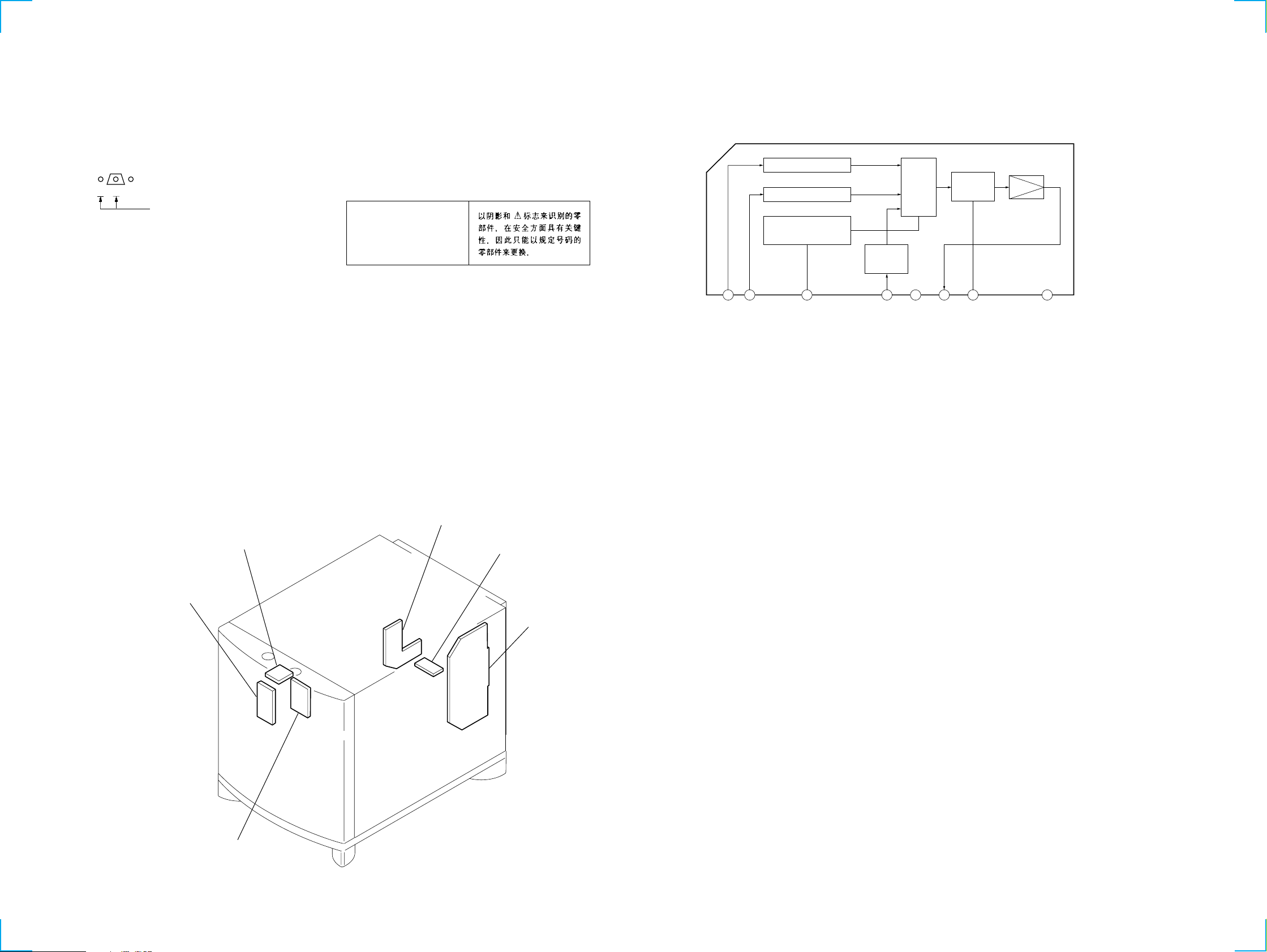
IC302 uPC1237HA
OVER LOAD DET
CC ON
OFFSET DET
LATCH/
AUTORESET
AC OFF
DET
1 2 3 4 5 6 7 8
F/F
V
MUTE
CC
V
• Circuit Boards Location
SA-WMS215
POWER SWITCH board
LED board
POWER SUPPLY board
POWER IC board
MAIN boar
CONTROL board
33
 Loading...