

Page 1
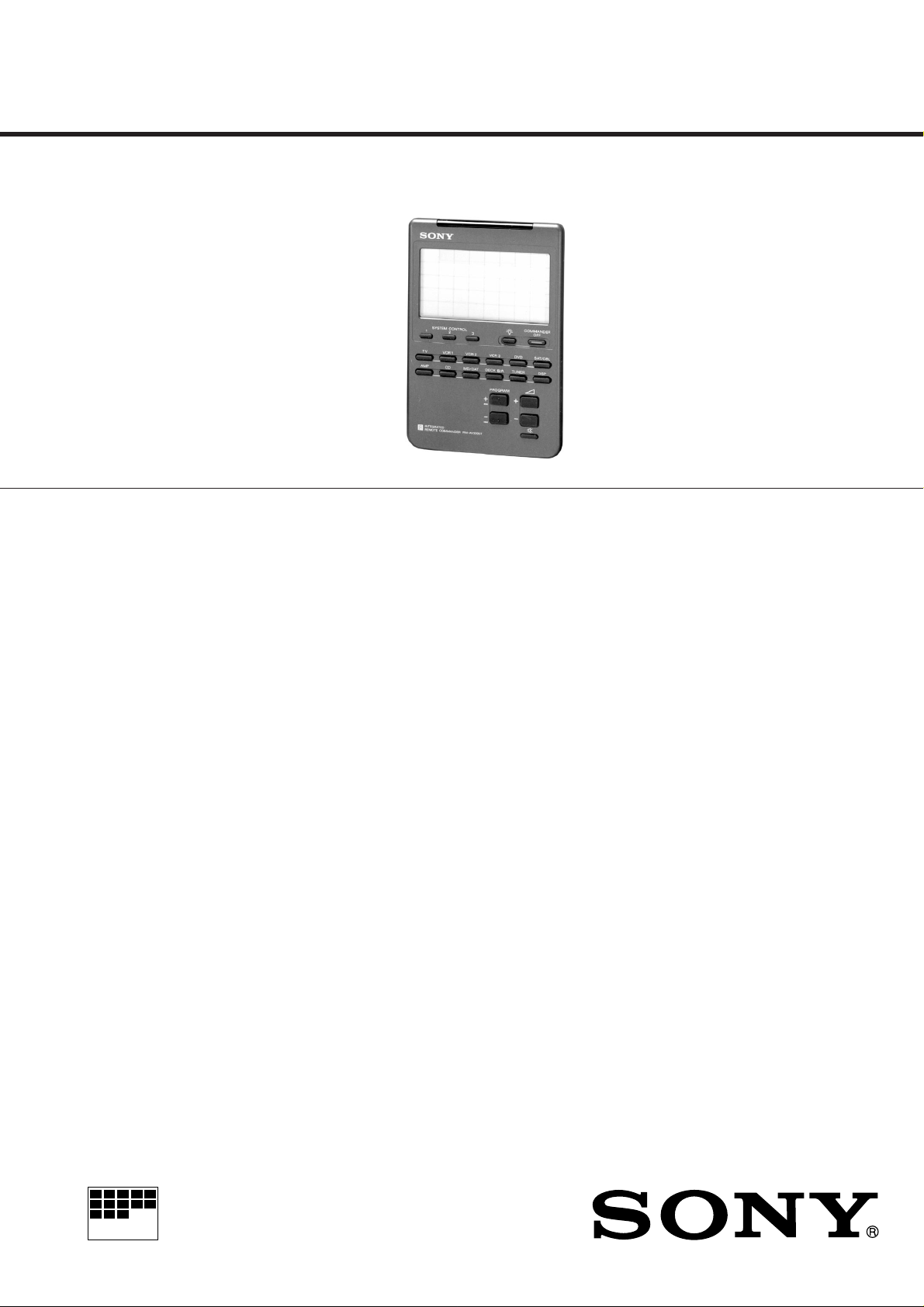
RM-AV2000T
MICROFILM
SERVICE MANUAL
SPECIFICATIONS
AEP Model
UK Model
E Model
Operating distance Approx. 10 meters (32.8 ft.) (varies
Power requirements Remote control : Four R6 (size AA)
batteries
Battery life Apporox. 6 months (varies depending on
Dimensions Approx. 120 × 175 × 45 mm
(43/4 × 7 × 113/16 in.) (w × h × d)
Mass 290g (10.22 oz.) (not including batteries)
Design and specifications are subject to change without notice.
depending on components of different
manufacturers)
Backlight : Two R6 (size AA) batteries
frequency of use)
INTEGRATED REMOTE COMMANDER
Page 2

TABLE OF CONTENTS
1. GENERAL ······································································3
2. DISASSEMBLY
2-1. Removal of case (lower)··················································· 15
2-2. Removal of T.T.P, LCD, rubber switch, main bard ·········· 15
3. TEST MODE ································································ 16
4. DIAGRAMS
4-1. Printed Wiring Board –Main Section– ····························· 19
4-2. Schematic Diagram –Main Section – ······························· 21
4-3. IC Pin Functions ······························································· 23
5. EXPLODED VIEWS ··················································26
6. ELECTRICAL PARTS LIST ··································· 27
SAFETY-RELATED COMPONENT WARNING!!
COMPONENTS IDENTIFIED BY MARK ! OR DO TTED LINE WITH
MARK ! ON THE SCHEMATIC DIAGRAMS AND IN THE PARTS
LIST ARE CRITICAL TO SAFE OPERATION. REPLACE THESE
COMPONENTS WITH SONY PARTS WHOSE PART NUMBERS
APPEAR AS SHOWN IN THIS MANUAL OR IN SUPPLEMENTS
PUBLISHED BY SONY.
— 2 —
Page 3
SECTION 1
GENERAL
This section is extracted
from instruction manual.
— 3 —
Page 4

— 4 —
Page 5
— 5 —
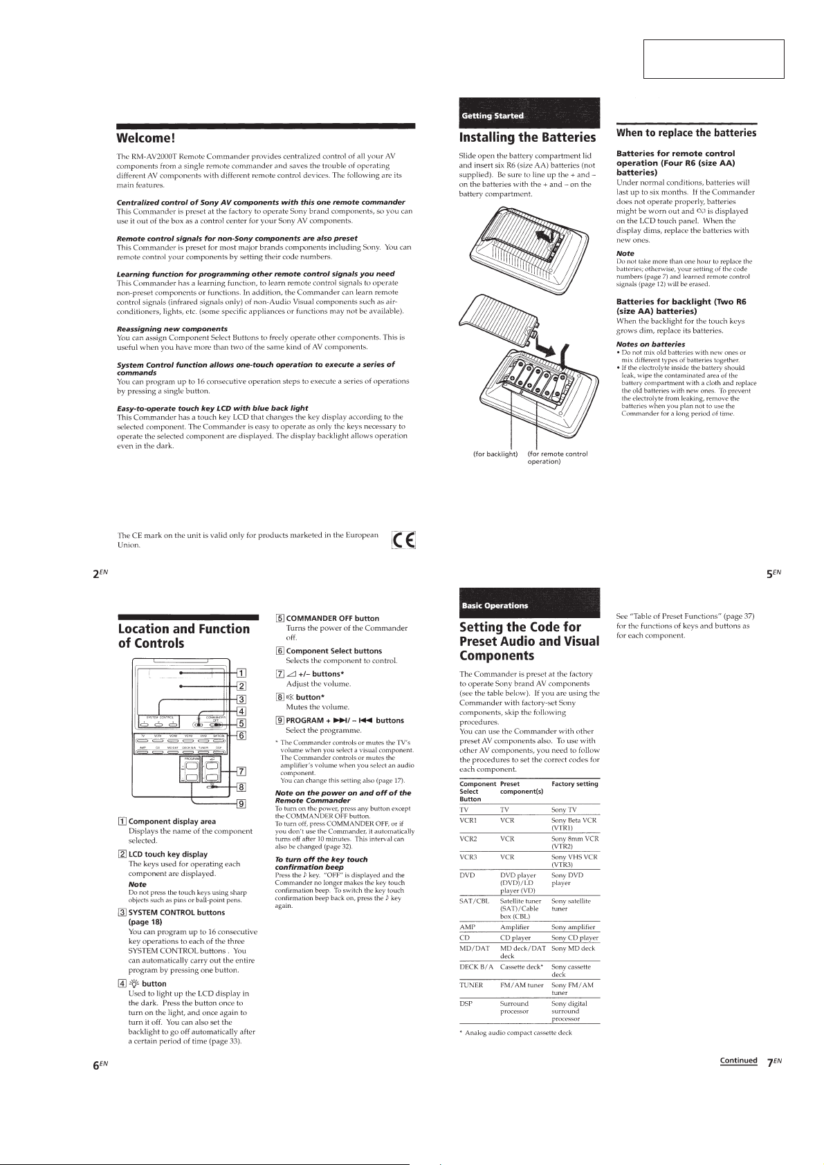
Page 6
— 6 —
Page 7
— 7 —
Page 8
— 8 —
Page 9

— 9 —
Page 10

— 10 —
Page 11

— 11 —
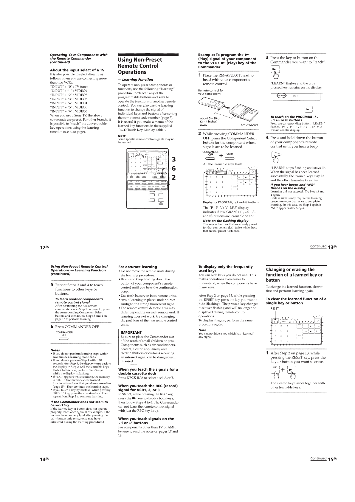
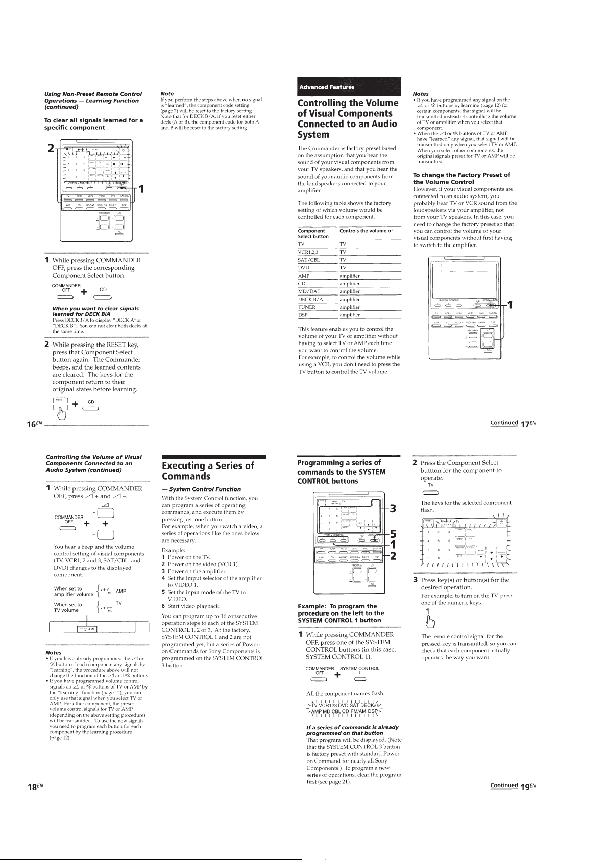
Page 12

— 12 —
Page 13

— 13 —
Page 14

— 14 —
Page 15

SECTION 2
)
e
DISASSEMBLY
Note: Follow the disassembly procedure in the numerical order given.
2-1. REMOVAL OF CASE (LOWER)
4
1
Battery lid
Case (upper)
Precision screwdriver
2
+K2 ×8
Case (lower)
Case (upper)
×
6
Claw
3
Insert a precision screwdriver tip in between the Case (upper
and the Case (lower). When the Cases are opened a little,
2
+K2 ×8
insert nail of your thumb into the clearance. Open the Covers
while sliding the Covers upwards.
2-2. REMOVAL OF T.T.P, LCD, RUBBER SWITCH, MAIN BOARD
2
Case (upper)
3
Remove soldering of th
T.T.P. and remove it.
4
LCD
5
Rubber switch
6
MAIN board
— 15 —
1
+P2 ×5
Case (lower)
Page 16

TEST Mode (Operation Check)
SECTION 3
TEST MODE
Preform the following operation checks using the TEST Mode before
starting the repair works.
1. All Keys Operation Check
Connection Method :
Regulated power supply
(+6V constant voltage output)
set
+6V pin
(See Fig. 3-1.)
1) While pressing the PROGRAM + key and the Á + key,
ture ON the main power of the regulated power supply (DC
+6V). (Refer to Fig. 1-1.)
2) Remove all hands from pressing the all keys described in abov e
step 1). The all indications of the LCD must be turned OFF.
(Refer to Fig. 1-2.)
3) When any key of the Operation panel-key block (except
the COMMANDER OFF key), or any key of the LCD touchkey block is pressed, the signal (carrier 40kHz) as shown in
Fig. 1-3 must be transmitted in accordance the pressed key , when
operation of the machine is normal.
4) Press all keys of the Operation panel-key block (except the
COMMANDER OFF key, and of the LCD touch-key block
sequentially. When all keys are pressed, confirm that the long
buzzar sound and all LCD displays are turned off.
NOTE : Be careful that all data in S-RAM is cleared
when the above TEST mode is performed.
+
–
LCD touch-key block
Operation
panel-key block
PROGRAM
+ +
While pressing both keys
at the same time;
COMMANDER OFF
Á
Fig. 1-1
PROGRAM +
Á
+
Turn ON the
main power (DC 6V)
• This TEST Mode can be terminated in its middle before testing
all keys by pressing the COMMANDER OFF key . However
the conduction check of the remairing keys cannot be checked.
(S-RAM is not cleared.)
• P-ROM (IC8) is diagnosed to be free from defects when the
steps from 1) to 4) are performed correctly.
Fig. 1-2
2.4mscc 2.4mscc 2.4mscc
600 µ sec 600 µ sec
— 16 —
Fig. 1-3
Page 17

2. S-RAM (Learning Function) Operation Check
y
Connection Method :
3. Oscillation frequency Check
Connection Method :
MAIN board
Regulated power supply
(+6V constant voltage output)
set
+6V pin
+
–
1) While pressing the Á – key and the PROGRAM – key,
ture ON the main power of the regulated power supply (DC
+6V). (Refer to Fig. 2-1.)
2) When LEARN only of the LCD display appears, remove
hands from pressing the above mentioned keys. (Refer to Fig.
2-2.)
3) The display appears when the S-RAM is not defective. (The
diaplay NG appears when the S-RAM is defective.) (Refer to
Fig. 2-2.)
4) The display status as described in step 3) continues until any
key is pressed.
• S-RAM (IC3) is diagnosed to be free from defects when the
above steps from 1) to 4) are performed correctly.
PROGRAM –
PROGRAM
– –
While pressing both keys at the same time;
Á
Turn ON the
regulated power suppl
Á
MAIN BOARD (CONDUCTOR SIDE)
–
TP GND
TP VDD
2140
41
20
Regulated
power supply
(DV +6V constant
voltage)
+
−
IC1
60
61
TP3
24
25
1
80
1
80
IC1 ^¡ pin
IC1 ^º pin
SW1
SW2
TP3
+
−
frequency cunter
IC2
40
41
65
64
(NG) (OK)
Fig. 2-1
Fig. 3-1
LEARN
1) After turning the switches SW1 and SW2 both ON, turn on the
main power of a frequency counter and that of the regulated
power supply (DC +6V constant voltage).
2) Take r eading of frequenc y counter indication value. This v alue
is named fA.
3) Turn off the regulated power supply, then turn OFF the switch
SW1. After that, turn back ON the regulated power supply.
4) Take reading of frequency counter value in the same way as
step 2). This value is named fB.
5) Using the frequency values that are measured in steps 2) and
After a while
4), calculate the crystal oscillator frequency f1 and the crystal
oscillator frequency f2 using the following equations. Confirm
that the respective specification values are satisfied.
LEARNLEARN NG
U
Specification values:
f1 (4 Mz) = fB x 8
f2 (32.768 kHz) = fA x 4
Fig. 2-2
— 17 — — 18 —
Page 18

RM-AV2000T
SECTION 4
DIAGRAMS
4-1. PRINTED WIRING BOARD – MAIN SECTION –
12
345678910111213
A
B
C
D
E
F
G
• Semiconductor
Location
• Semiconductor Location
Ref. No. Location
D1 B-10
D2 B-9
D3 B-8
D4 B-7
D5 E-10
D6 A-9
D10 E-10
D11 E-10
IC1 B-9
IC2 D-8
IC3 E-9
IC4 B-10
IC5 E-10
Ref. No. Location
Ref. No. Location
IC6 B-8
IC7 C-9
IC8 E-8
Q1 B-9
Q2 B-7
Q4 E-10
Q9 D-9
Q10 D-10
Q11 E-10
Q12 D-9
Q13 D-9
Q14 F-9
Q15 F-9
— 19 — — 20 —
Note:
• X : parts extracted from the component side.
®
•
• b : Pattern from the side which enables seeing.
(The other layers' patterns are not indicated.)
Caution:
Pattern face side: Parts on the pattern face side seen from
(Conductor Side) the pattern face are indicated.
Parts face side: Parts on the parts face side seen from
(Component Side) the parts face are indicated.
• b : Switch pattern
: Through hole.
Page 19

4-2. SCHEMATIC DIAGRAM – MAIN SECTION – • See Page 23, 25 IC Pin Function.
RM-AV2000T
A
B
C
D
E
12
MAIN BOARD
D.SKIP
12 3
45 6
78 9
-/--
0
1-
CLEAR
ENTER
LCD1
u
CD
PGM
CONTINUE
REPEAT
SHUFFLE
2.4
2.5
2.5
8078797677747572737071
S8
S9
S11
2.5
2.4
2.5
2.5
2.5
2.5
2.5
2.5
2.5
2.5
2.4
2.5
2.4
2.5
2.4
2.4
2.4
2.5
2.4
2.5
S10
S12
1
S13
2
S14
3
S15
4
S16
5
S17
6
S18
7
S19
8
S20
9
S21
10
S22
11
S23
12
S24
13
S25
14
S26
15
S27
16
S28
17
S29
18
S30
19
S31
20
COM1
COM0
COM2
2123222524272629283130
2.5
2.5
C15
0.01
C16
0.01
C17
0.01
R41
100K
2.5
COM3
2.5
34567891011121314
2.5
S7
BIAS
5.0
R39
100k
R40
100k
S6
VLC0
5.0
2.402.402.5
S2
S3
S4
S5
IC1
SYSTEM CONTROL
IC1
uPD753017AGCE11
VLC2
VLC1
P41
P40
3.3
1.6
JP3
5.0
5.002.402.4
696768656663646162
S0
S1
P42
P71
P72
P73
RESET
P43
P50
VSS
P52
P51
323433363538374039
00000
TTP52
TTP51
TTP50
TTP43
5.0
P70
1
P53
0
P63
P00/INT4
TTP53
P62
P01
B+
5.0
TPBZ
3.0
RES
IP46
4.9
TPEL0
4.905.0
CLR
ICLK
OP67
uPD65012GF251
IP47
KINT
5.0
4.9
R50
4.7K
5.0
5.0
5.0
OP65
OP66
IC2
GATE ALLEY
IC2
IP50
IP52
IP51
5.0
5.0
R51
10k
VDD
GND
5.0
R57
BZ1
Q9
MSD601
BUZZER DRIVE
5.0
5.000
X1
P61
P60
X2
X1
VPP
XT2
XT1
VDD
P33
P32
P31
P30
P23
P22
P21
P20
P13
P12
P11
P10
P03
P02
4.9
5.0
TPOSC1
5.0
3.0
2.4
5.0
2.6
1.7
5.0
4.9
4.9
4.9
4.9
0
5.0
5.0
0
5.0
4.9
5.0
0
4.9
TPLCD
R21 330k
TPBATT
TPRES
R20
100K
C10
0.047
4.0MHz
C13 33p
IRDN
IWIN
IENN
4.9
R84
0
60
59
58
57
56
55
54
53
52
51
50
49
48
47
46
45
44
43
0
41
32.768kHz
C14 33p
ADB
R22 27
ADA
AD9
AD8
TP3
IC6
IC6
RN5VL45CTR
5.0
1 2
3
IC7
RN5VL40ATR
1 2
3
R19
100K
C12
0.01
X2
BATT
DOWN
5.0
C11
470
10V
IC7
5.0
RESET
5.0
P73
1
5.0
P72
2
5.0
P71
3
5.0
P70
4
5.0
P63
5
5.0
P62
6
5.0
P61
7
5.0
P60
8
0
P20
9
5.0
P21
10
5.0
P22
11
0
12
4.9
13
4.9
14
4.9
15
4.9
16
4.9
17
4.9
B+
18
4.9
19
4.9
20
4.9
21
4.9
22
4.9
23
4.9
1k
5.0
0
R56
4.7K
0
5.0
8078797677747572737071
INT
IALK
ID7
ID6
ID5
ID4
ID3
ID2
ID1
ID0
IENN
IWIN
IRDN
GND
IP30
IP31
IP32
IP33
IP34
IP35
IP36
IP37
IP40
IP41
IP42
IP43
IP45
IP44
2524272629283130323433363538374039
4.9
4.9
MSB709
TPEL1
5.0
GND
VDD
5.0
Q10
0
R52
470
Q10,11
EL SWITCH
(BRIGHT)
69
OP63
OP64
IP54
IP53
5.0
MSD602
68
OP62
IP55
5.0
Q11
2.7
5.00000
67
OP61
IP56
5.0
5.0
66
OP60
REC
R53
4.7k
MSB709
65
RMO
RDO
5.0
5.0
Q12
OUTP
ADA
ADB
AD9
AD8
AD7
AD6
AD5
AD4
AD3
AD2
GND
AD1
AD0
OD7
OD6
OD5
OD4
OD3
OD2
OD1
OD0
OCE
WTO
0
5.0
D11
MA738
MA738
0
0
R55
470
R54
10k
MSD602
64
4.9
63
4.9
62
4.9
61
4.9
60
5.0
59
5.0
58
1.1
57
1.1
56
4.1
55
4.1
54
53
1.2
52
0
51
2.0
50
3.8
49
2.7
48
2.0
47
3.8
46
0.2
45
3.8
44
3.0
43
5.0
42
5.0
41
TPREC
Q12,13
EL SWITCH
(DARK)
D10
2.7
Q13
TPVDD3
DC1.5X2
10V
R61
R60
82
1.5k
3.1
TPELOSC
2.8
3.1
Q14
MSD1328
SWITCHING
C20
OSC
470
0
1
5.0
2
ADC
5.0
AD7
3
5.0
AD6
4
1.1
AD5
5
1.1
AD4
6
4.1
AD3
7
4.1
AD2
8
1.2
AD1
9
0
AD0
10
3.0
OP0
11
3.8
OP1
12
0.2
OP2
13
GND
14
C23
10
16V
C22
0.1
IC3
SRAM
IC3
W24257S
L1
1
2
3
4
5
6
12
11
8
7
TPEGND
VCC
WE
ADD
AD8
AD9
ADB
OE
ADA
CE1
OP7
OP6
OP5
OP4
OP3
TPELOUT
TPSEL
C3
TPGC
0.01
4.8
28
5.0
27
0
26
4.9
25
4.9
24
4.9
23
0
22
4.9
21
0
20
2.0
19
3.8
18
2.7
17
2.0
16
3.8
15
C4(GC)
0.047F
64K-256K
JP1 JP2
R10
10K
0
0
Q4
MSD601
INVERTER
D5
1SS294
0
R8
15K
R9
47K
EL
F
G
H
J
TPVDD
DC 1.5X4
TPGND
IC5
RH5RE50AA
2 3
1
5.06.0
TPVDD2
IC5
REGULATOR
0.01
C2
C6
3300p
C5
220p
PRE AMP
uPD4069UBG
4.5
1
4.5
2
4.5
3
4.5
4
4.5
5
4.5
6
5.0 4.9
7
C7 0.047
R12
10k
R13
10k
R14
2.2M
R11
6.8k
R15
39k
IC4
B+
5
MSD601
SELECT
SWITCH
Q15
CHIP
R70 10K
R72
47K
0
R71
15K
D6
TPS705
IC4
5.0
14
5.0
13
12
5.0
11
4.7
10
9
4.7
B+
R18
120k
B+
0.01
5.0
1
5.0
2
ADC
AD7
AD6
AD5
AD4
AD3
AD2
AD1
AD0
OP0
OP1
OP2
GND
IC8
ROM
IC8
LH5359PA
5.0
3
5.0
4
1.1
5
1.1
6
4.1
7
4.1
C9
8
1.2
9
0
10
3.0
11
3.8
12
0.2
13
14
VCC
ADE
ADD
AD8
AD9
ADB
ADA
CE1
OP7
OP6
OP5
OP4
OP3
5.0
28
0
27
0
26
4.9
25
4.9
24
4.9
23
0
22
OE
4.9
21
5.0
20
2.0
19
3.8
18
2.7
17
2.0
16
3.8
15
8
R16 560
R17 27k
C8
TPCONT
0.047
• Voltages and waveforms are dc with respect to ground
under no-signal (detuned) conditions.
• Voltages and waveforms are dc with respect to ground in
playback mode.
• Voltages are taken with a VOM (Input impedance 10 MΩ).
Voltage variations may be noted due to normal production tolerances.
• Waveforms are taken with a oscilloscope.
• Circled numbers refer to wave forms.
TTP
R3
470
00
Q1,2
LED DRIVE
R1
8.2
TPR1
D1
D2
Q1
MSD1328
C1
100
10V
R2
S2-10
u
R31
S2-2
B+
R32
R33
R34
R35
R36
R37
R38
100K*8
RESET
S2-1
S2-9
DISPLAY
S2-8
INPUT
S2-7
RED
S2-6
3
S2-5
2
S2-4
1
S2-3
S2-18
S2-17
ANGLE
S2-16
TV
S2-15
GREEN
S2-14
6
S2-13
5
S2-12
4
S2-11
EXECUTE
S2-26
PGM
S2-25
MENU
S2-24
TELE TEXT
S2-23
YELLOW
S2-22
9
S2-21
8
S2-20
7
S2-19
S2-34
CONTINUE
S2-33
S2-32
RETURN
S2-31
T.TONE
S2-30
ENTER
S2-29
0
S2-28
-/--
S2-27
IP40
IP41
IP42
IP43
IP44
IP45
IP46
IP47
COMMANDER OFF
R23
R24
R25
SYSTEM
CONTROL3
R26
S1-3
SYSTEM
CONTROL2
R27
S1-2
SYSTEM
CONTROL1
R28
R29
B+
R30
100K*8
S1-5
S1-4
SAT/CBL
S1-11
S1-10
S1-9
S1-8
S1-7
S1-6S1-1
DVD
VCR3
VCR2
VCR1
TV
DSP
S1-17
DECK B/A
S1-15
MD/DAT
S1-14
CD
S1-13
TUNER
S1-16
AMP
S1-12
S1-22
Á Á¤
PROGRAM PROGRAM
S1-18
S1-21S1-19
S1-20
IP30
TPP30
IP31
TPP31
IP32
TPP32
IP33
TPP33
IP34
TPP34
IP35
TPP35
IP36
TPP36
IP37
TPP37
B+
TPRMO
R4
470
Q2
MSD1328
8.2
TPR2
D3
D4
4.0 4.0
D1-D4
UR64LD1
I
16
• Waveform
1 IC1 %∞
32.768kHz
2.8Vp-p
Note:
• All capacitors are in µF unless otherwise noted. pF: µµF
50 WV or less are not indicated except for electrolytics
and tantalums.
• All resistors are in Ω and 1/4 W or less unless otherwise
specified.
• C : panel designation.
• U : B+ Line.
• Power voltage is dc 6V and fed with regulated dc power
supply from battery terminal.
— 21 — — 22 —
Page 20

4-3. IC PIN FUNCTION
• IC1 (µPD753017)
µPD753017 is the 4-bit single-chip microprocessor for the LCD panel display with the built-in controller and driver.
Pin No.
1 to 12
13 to 20
21 to 24
25
26 to 28
29 to 32
33
34 to 37
38
39
40
41
42
43
44
45
46
47
48
49
50
51
52
53
Pin Name
S12 to S23
BP0 to BP7/
S24 to S31
COM0 to COM3
BIAS
VLC0 to VLC2
P40 to P43
Vss
P50 to P53
P00/INT4
P01/SCK
P02/SO/SB0
P03/S1/SB1
P10/INT0
P11/INT1
P12/INT2
P13/TIO
P20/PTO0
P21/PTO1
P22/PCL
P23/BUZ
P30/LCD CL
P31/SYNC
P32
P33
I/O
O
Segment signal output terminals.
O
1-bit output port (BIT-PORT). Used also as the segment signal output terminal.
O
Common signal output terminal.
O
Output terminal for cutting off the externally connected dividing resistor.
–
Power supply terminal for LCD drive. Dividing resistor are built-in. (mask option)
N-ch open-drain 4-bit input/output port. (PORT 4).
I/O
Pull-up resistor can be built-in in units of bit. (mask option).
10V withstand voltage in the open-drain connection.
–
GND terminal.
N-ch open-drain 4-bit input/output port. (PORT 5).
I/O
Pull-up resistor can be built-in in units of bit. (mask option).
10V withstand voltage in the open-drain connection.
Edge detection vector interrupt input terminal.
I
(Both of the rise-up and fall-down edge detections are usable.)
I/O
Serial clock input/output terminal.
Serial data output terminal.
I/O
Serial bus input/output terminal.
Serial data input terminal.
I/O
Serial bus input/output terminal.
Equipped with noise-rejection function.
I
Clock-synchronous type.
I
Asynchronous
Edge detection teatble input terminal.
I
(Rise-up edge detection). Asynchronous.
External event pulse input
I
terminal to the timer/event counter.
I/O
Timer/event counter output terminal.
I/O
Timer/event counter output terminal.
I/O
Clock output terminal.
Fixed frequency output terminal.
I/O
(For buzzer or for trimming the system clock.
I/O
Clock output terminal for driving the external expansion driver.
I/O
Clock output terminal for synchronizing the external expansion driver.
I/O
I/O
Pin Function
Edge detection vector interrupt
input terminal.(Detection edge
selectable.)
4-bit input port (PORT 0).
The pull-up resistor built-in can be
specified in units of 3 bits by
software for PO1 to PO3.
4-bit input port (PORT 1).
The pull-up resistor built-in can
be specified in units of 4 bits by
software.
4-bit input port (PORT 2).
The pull-up resistor built-in can be
specified in units of 4 bits by
software.
Programmable 4-bit input/output
port. (PORT 3).
Input and output can be set in units
of bit.
The pull-up resistor built-in can be
specified in units of 4 bits by
software.
Pin No.
54
55
56
57
58
59
60
61
62
63
64
65
66
67
68
69 to 80
Pin Name
VDD
XT1
XT2
VPP
X1
X2
P60/KR0
P61/KR1
P62/KR2
P63/KR3
P70/KR4
P71/KR5
P72/KR6
P73/KR7
RESET
S0 to S11
I/O
–
Positive power supply terminal.
Terminal to which sub-system clock oscillating crystal is connected.
I
When external clock is used, input the ext. clock to XT1 and leave XT2 open.
–
XT1 can be used as the 1-bit input (TEST) terminal.
–
Internally connected to VDD.
I
Terminal to which main system clock oscillating crystal/ceramic is connected.
–
When external clock is used, input the ext. clock to X1, and connect the inverted phase signal to XT2.
I/O
I/O
Parallel fall-down edge detection
I/O
testable input terminal.
I/O
I/O
I/O
Parallel fall-down edge detection
testable input terminal.
I/O
I/O
System reset input terminal.
I
Segment signal output terminals.
O
Pin Function
Programmable 4-bit input/output port. (PORT 8).
Input and output can be specified in units of bit.
The pull-up resistor built-in can be specified in units of
4 bits by software.
4-bit input/output port. (PORT 7).
The pull-up resistor built-in can be specified in units of
4 bits by software.
— 23 — — 24 —
Page 21

• IC2 (µPD65012)
Pin No.
1 to 8
9 to11
12
13 to 20
21 to 28
29
30 to 32
33
34
35 to 38
39
40 to 42
43 to 50
51 to 52
53
54 to 59
60 to 63
64
65
66
67
68
69
70
71
72
73
74
75
76
77
78
79
80
Pin Name
ID7 to ID0
IENN/IWIN
IRDN.
GND
IP30 to IP37
IP40 to IP47
KINT
IP50 to IP52
GND
VDD
KINT
IP53 to IP56
REC
RDO.WTO
OCE
OD0 to OD7
AD0 to AD1
GND
AD2 to AD7
AD8 to AD11
OUTP
RMO
OP60
OP61
OP62
OP63
OP64
GND
VDD
OP65
OP66
OP67
CLR
ICLK
RES
INT
IALE
I/O
I/O
Data transfer between µPD65012 and microprocessor.
I
Control input from microprocessor.
—
GND terminal.
I
Key scan input.
I
Key scan input.
I
Not used.
—
GND terminal.
—
Positive power supply terminal.
I
Not used.
I
Remote control signal received input.
O
External memory control output.
I/O
Data transfer between µPD65012 and external memory.
O
Terminals to which external memory is connected. Lower address (ADO to AD1)
—
GND terminal.
O
Terminals to which external memory is connected. Lower address (AD2 to AD7)
O
Terminals to which external memory is connected. Upper address (AD8 to AD11)
O
Not used.
O
Remote control signal output.
O
Remote control signal receiver block ON/OFF output.
O
SRAM IC3 (W24257S) ADD and IC8 (LH5359PA) ADD.
O
SRAM IC3 (W24257S) ADE and IC8 (LH5359PA) ADE.
O
Selector SRAM IC3 (W242575S) or ROM IC8 (LH5359PA)
O
EL control output. (Dark)
—
GND terminal.
—
Positive power supply terminal.
O
Terminals to which external memory is connected. Upper address. (AD12)
O
EL control output. (Bright).
O
Buzzer
I
GA reset input.
I
GA clock input.
I
Not used.
O
Microprocessor interrupt output.
I
Address latch enable input.
Pin Function
— 25 —
Page 22

SECTION 5
EXPLODED VIEWS
NOTE:
• -XX, -X mean standardized parts, so they may
have some differences from the original one.
• Items marked “*” are not stocked since they
are seldom required for routine service. Some
delay should be anticipated when ordering these
items.
2
• The mechanical parts with no reference number
in the exploded views are not supplied.
12
19
The components identified by mark ! or
dotted line with mark ! are critical for safety .
Replace only with part number specified.
11
10
22
9
21
EL1
6
8
20
17
18
7
16
15
14
1
1
23
5
3
4
13
Ref. No. Part No. Description Remarks Ref. No. Part No. Description Remarks
1 7-685-205-19 SCREW +KTP2 × 8 TYPE2 NON-SLIT
* 2 9-880-055-01 HOLDER
3 9-880-050-01 LID, BATTERY CASE
4 7-685-103-19 SCREW +P2 × 5 TYPE2 NON-SLIT
5 9-995-523-01 FOOT, RUBBER
13 9-995-521-01 COMMON TERMINAL
* 14 9-995-529-01 TERMINAL (+)
15 9-995-522-01 COMMON TERMINAL
* 16 9-995-530-01 TERMINAL (–)
* 17 9-995-528-01 TERMINAL (+)
6 9-880-048-01 RUBBER SWITCH
7 9-880-049-01 CASE (LOWER)
* 8 9-880-057-01 SPACER
* 9 9-995-525-01 LCD BRACKET
* 10 9-880-051-01 SEAL
11 9-995-518-01 SMOKE PLATE
12 9-880-458-01 CASE (UPPER)
* 18 9-995-531-01 TERMINAL (–)
* 19 9-880-053-01 ZEBRA CONNECTOR
* 20 9-880-235-01 MAIN BOARD, COMPLETE
21 9-880-459-01 LCD
22 9-880-056-01 TTP
23 9-880-460-01 LABEL, CE
EL1 9-880-153-01 ELECTRO LUMINESCENT
— 26 —
Page 23

SECTION 6
ELECTRICAL PARTS LIST
MAIN
NOTE:
The components identified by mark ! or
dotted line with mark ! are critical for safety .
Replace only with part number specified.
Ref. No. Part No. Description Remarks Ref. No. Part No. Description Remarks
* 9-880-235-01 MAIN BOARD,COMPLETE
********************
< BUZZER >
BZ1 9-880-012-01 BUZZER
< CAPACITOR >
C1 1-104-658-91 ELECT 100uF 20% 10V
C2 1-104-329-11 CERAMIC CHIP 0.01uF 10% 50V
C3 1-104-329-11 CERAMIC CHIP 0.01uF 10% 50V
C4 9-880-016-01 GOLD CAP 0.047F
C5 1-163-001-11 CERAMIC CHIP 220PF 10% 50V
C6 1-163-015-91 CERAMIC CHIP 3300PF 10% 100V
C7 1-104-760-11 CERAMIC CHIP 0.047uF 10% 50V
C8 1-104-760-11 CERAMIC CHIP 0.047uF 10% 50V
C9 1-104-329-11 CERAMIC CHIP 0.01uF 10% 50V
C10 1-104-760-11 CERAMIC CHIP 0.047uF 10% 50V
C11 1-126-925-11 ELECT 470uF 20% 10V
C12 1-104-329-11 CERAMIC CHIP 0.01uF 10% 50V
C13 1-162-642-91 CERAMIC CHIP 33PF 5% 50V
C14 1-162-642-91 CERAMIC CHIP 33PF 5% 50V
C15 1-104-329-11 CERAMIC CHIP 0.01uF 10% 50V
C16 1-104-329-11 CERAMIC CHIP 0.01uF 10% 50V
C17 1-104-329-11 CERAMIC CHIP 0.01uF 10% 50V
C20 1-126-925-11 ELECT 470uF 20% 10V
C22 1-115-339-11 CERAMIC CHIP 0.1uF 10% 50V
C23 1-126-964-11 ELECT 10uF 20% 50V
< CONNECTOR >
* CN1 9-880-019-01 CONNECTOR 14P
* CN2 9-880-018-01 CONNECTOR 4P
• Due to standardization, replacements in the
parts list may be different from the parts
specified in the diagrams or the components
used on the set.
• -XX, -X mean standardized parts, so they may
have some difference from the original one.
• Items marked “*” are not stocked since they
are seldom required for routine service. Some
delay should be anticipated when ordering these
items.
• CAPA CITORS:
uF: µF
IC6 9-880-042-01 IC RN5VL45CTR
IC7 9-880-041-01 IC RN5VL40ATR
IC8 9-880-456-01 IC LH5359PA
* L1 9-880-011-01 TRANSFORMER EL TRANSFORMER
Q1 9-880-040-01 TRANSISTOR MSD1328RT1
Q2 9-880-040-01 TRANSISTOR MSD1328RT1
Q4 8-729-010-25 TRANSISTOR MSD601-RT1
Q9 8-729-010-25 TRANSISTOR MSD601-RT1
Q10 8-729-010-05 TRANSISTOR MSB709-RT1
Q11 8-729-010-35 TRANSISTOR MSD602-RT1
Q12 8-729-010-05 TRANSISTOR MSB709-RT1
Q13 8-729-010-35 TRANSISTOR MSD602-RT1
Q14 9-880-040-01 TRANSISTOR MSD1328RT1
Q15 8-729-010-25 TRANSISTOR MSD601-RT1
R1 1-247-302-11 CARBON 8.2 5% 1/4W
R2 1-247-302-11 CARBON 8.2 5% 1/4W
R3 1-216-041-00 RES,CHIP 470 5% 1/10W
R4 1-216-041-00 RES,CHIP 470 5% 1/10W
R8 1-216-077-00 RES,CHIP 15K 5% 1/10W
R9 1-216-089-91 RES,CHIP 47K 5% 1/10W
R10 1-216-073-00 RES,CHIP 10K 5% 1/10W
R11 1-216-069-00 RES,CHIP 6.8K 5% 1/10W
R12 1-216-073-00 RES,CHIP 10K 5% 1/10W
R13 1-216-073-00 RES,CHIP 10K 5% 1/10W
• RESISTORS
All resistors are in ohms.
METAL: metal-film resistor
METAL OXIDE: Metal Oxide-film resistor
F: nonflammable
• COILS
uH: µH
• SEMICONDUCTORS
In each case, u: µ, for example:
uA...: µA... , uPA... , µPA... ,
uPB... , µPB... , uPC... , µPC... ,
uPD..., µPD...
< COIL >
< TRANSISTOR >
< RESISTOR >
< DIODE >
D1 9-880-014-01 DIODE UR64LD1
D2 9-880-014-01 DIODE UR64LD1
D3 9-880-014-01 DIODE UR64LD1
D4 9-880-014-01 DIODE UR64LD1
D5 8-719-938-72 DIODE SB01-05CP
D6 9-880-013-01 DIODE TPS705WMATU2
D10 8-719-421-51 DIODE MA738-TX
D11 8-719-421-51 DIODE MA738-TX
< IC >
IC1 9-880-457-01 IC uPD753017E11
IC2 9-995-541-01 IC uPD65012F251
IC3 9-880-455-01 IC W24257S70LL
IC4 8-759-009-10 IC MC14069UBF
IC5 8-759-512-51 IC RH5RE50AA
R14 1-216-129-00 RES,CHIP 2.2M 5% 1/10W
R15 1-216-087-91 METAL,CHIP 39K 0.5% 1/10W
R16 1-216-043-91 RES,CHIP 560 5% 1/10W
R17 1-216-083-00 RES,CHIP 27K 5% 1/10W
R18 1-216-099-00 RES,CHIP 120K 5% 1/10W
R19 1-216-097-91 RES,CHIP 100K 5% 1/10W
R20 1-216-097-91 RES,CHIP 100K 5% 1/10W
R21 1-216-109-00 RES,CHIP 330K 5% 1/10W
R22 1-216-011-00 RES,CHIP 27 5% 1/10W
R23 1-216-097-91 RES,CHIP 100K 5% 1/10W
R24 1-216-097-91 RES,CHIP 100K 5% 1/10W
R25 1-216-097-91 RES,CHIP 100K 5% 1/10W
R26 1-216-097-91 RES,CHIP 100K 5% 1/10W
R27 1-216-097-91 RES,CHIP 100K 5% 1/10W
R28 1-216-097-91 RES,CHIP 100K 5% 1/10W
— 27 —
Page 24

RM-AV2000T
MAIN
Ref. No. Part No. Description Remarks Ref. No. Part No. Description Remarks
R29 1-216-097-91 RES,CHIP 100K 5% 1/10W
R30 1-216-097-91 RES,CHIP 100K 5% 1/10W
R31 1-216-097-91 RES,CHIP 100K 5% 1/10W
R32 1-216-097-91 RES,CHIP 100K 5% 1/10W
R33 1-216-097-91 RES,CHIP 100K 5% 1/10W
R34 1-216-097-91 RES,CHIP 100K 5% 1/10W
R35 1-216-097-91 RES,CHIP 100K 5% 1/10W
R36 1-216-097-91 RES,CHIP 100K 5% 1/10W
R37 1-216-097-91 RES,CHIP 100K 5% 1/10W
R38 1-216-097-91 RES,CHIP 100K 5% 1/10W
R39 1-216-097-91 RES,CHIP 100K 5% 1/10W
R40 1-216-097-91 RES,CHIP 100K 5% 1/10W
R41 1-216-097-91 RES,CHIP 100K 5% 1/10W
R50 1-216-065-00 RES,CHIP 4.7K 5% 1/10W
R51 1-216-073-00 RES,CHIP 10K 5% 1/10W
R52 1-216-041-00 RES,CHIP 470 5% 1/10W
R53 1-216-065-00 RES,CHIP 4.7K 5% 1/10W
R54 1-216-073-00 RES,CHIP 10K 5% 1/10W
R55 1-216-041-00 RES,CHIP 470 5% 1/10W
R56 1-216-065-00 RES,CHIP 4.7K 5% 1/10W
R57 1-216-049-91 RES,CHIP 1K 5% 1/10W
R60 1-216-053-00 RES,CHIP 1.5K 5% 1/10W
R61 1-216-022-91 RES,CHIP 82 5% 1/10W
R70 1-213-073-91 RES,CHIP 10K 5% 1/10W
R71 1-216-077-00 RES,CHIP 15K 5% 1/10W
6 9-880-048-01 RUBBER SWITCH
13 9-995-521-01 COMMON TERMINAL
* 14 9-995-529-01 TERMINAL (+)
15 9-995-522-01 COMMON TERMINAL
* 16 9-995-530-01 TERMINAL (–)
* 17 9-995-528-01 TERMINAL (+)
* 18 9-995-531-01 TERMINAL (–)
* 19 9-880-053-01 ZEBRA CONNECTOR
21 9-880-459-01 LCD
22 9-880-056-01 TTP
EL1 9-880-153-01 ELECTRO LUMINESCENT
************************************************************
3-862-795-11 INSTRUCTION (CORD LIST)
MISCELLANEOUS
**************
ACCESSORIES & PACKING MATERIALS
********************************
3-862-793-11 MANUAL,INSTRUCTION (English,Dutch)
3-862-793-21 MANUAL,INSTRUCTION (German,Spanish)
3-862-793-31 MANUAL,INSTRUCTION (French,Italian)
3-862-793-41 MANUAL,INSTRUCTION (Swedish,Finnish)
R72 1-216-089-91 RES,CHIP 47K 5% 1/10W
R84 1-216-295-91 CONDUCTOR,CHIP 0
< VIBRATOR >
X1 9-880-017-01 VIBRATOR,CERAMIC (4.00MHz)
X2 9-880-015-01 VIBRATOR,CRYSTAL (32.768kHz)
***********************************************************
9-923-336-11
Sony Corporation
Personal A&V Products Company
— 28 —
Printed in Japan © 1998.2
98B1666-1
Published by Quality Engineering Dept.
(Shibaura)
 Loading...