

Sony PVM-2530, RM-739 Service Manual
!
)
r
>
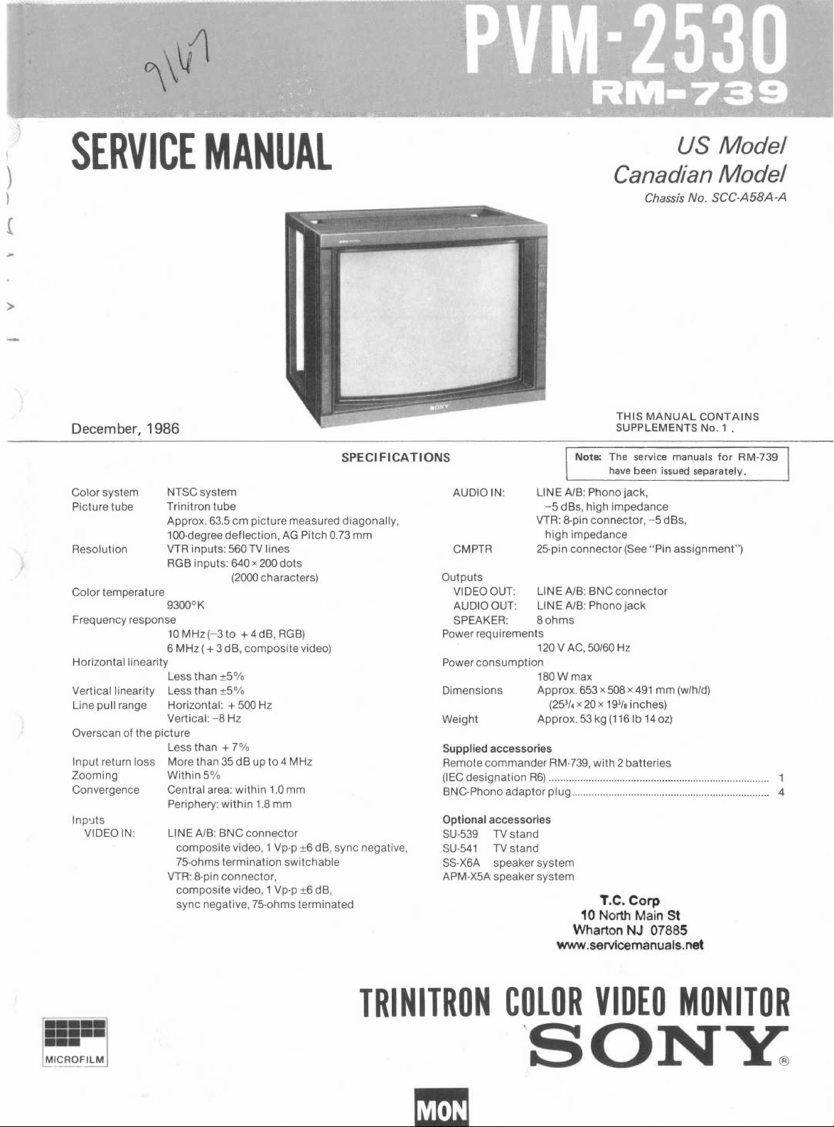
SERVICE MANUAL
December, 1986
US Model
Canadian Model
Chassis No. SCC-A58A-A
THIS MANUAL CONTAINS
SUPPLEMENTS No. 1 .
Color system
Picture tube
Resolution
Color temperature
Frequency response
Horizontal linearity
Vertical linearity
Line pull range
Overscan of the picture
Input return loss More than 35 dB up to 4 MHz
Zooming Within 5%
Convergence Central area: within 1.0 mm
lnp•JtS
VIDEO IN: LINE A/B: BNC connector
NTSC system
Trinitron tube
Approx. 63.5 cm picture measured diagonally,
100-degree deflection, AG Pitch 0.73 mm
VTR inpl!.lts: 560 TV lines
RGB inputs: 640 x 200 dots
(2000 characters)
9300°K
10 MHz (-3 to + 4 dB, RGB)
6 MHz ( + 3 dB, composite video)
Less than ±5%
Less than ±5%
Horizontal: + 500 Hz
Vertical: -8 Hz
Less than + 7%
Periphery: within 1.8 mm
composite video, 1 Vp-p ±6 dB, sync negative ,
75-ohms termination switchable
VTR: 8-pin connector,
composite video, 1 Vp-p ±6 dB,
sync negative, 75-ohms terminated
SPECIFICATIONS
Note; The service manuals for RM-739
have been issued separately.
AUDIO IN: LINE A/B: Phono jack,
CMPTR 25-pin connector (See "Pin assignment")
Outputs
VIDEO OUT: LINE A/B: BNC connector
AUDIO OUT: LINE A/B: Phono jack
SPEAKER: 8 ohms
Power requirements
Power consumption
Dimensions Approx. 653 x 508 x 491 mm (w/h/d)
Weight Approx. 53 kg (116 lb 14 oz)
Supplied accessories
Remote commander RM-739, with 2 batteries
(IEC designation R6) ............................................................................. .
BNC-Phono adaptor plug ...................................................................... 4
Optional accessories
SU-539 TV stand
SU-541 TV stand
SS-X6A speaker system
APM-X5A speaker system
-5 dBs, high impedance
VTR: 8-pin connector, -5 dBs,
high impedance
120 V AC, 50/60 Hz
180W max
(25¾ x 20 x 19
3
/a inches)
T.C. Corp
10 North Main St
Wharton NJ 07885
WWW .servicemanuals. net
TRINITRON COLOR VIDEO MONITOR
'SONY.
PVM-2530
RM-739
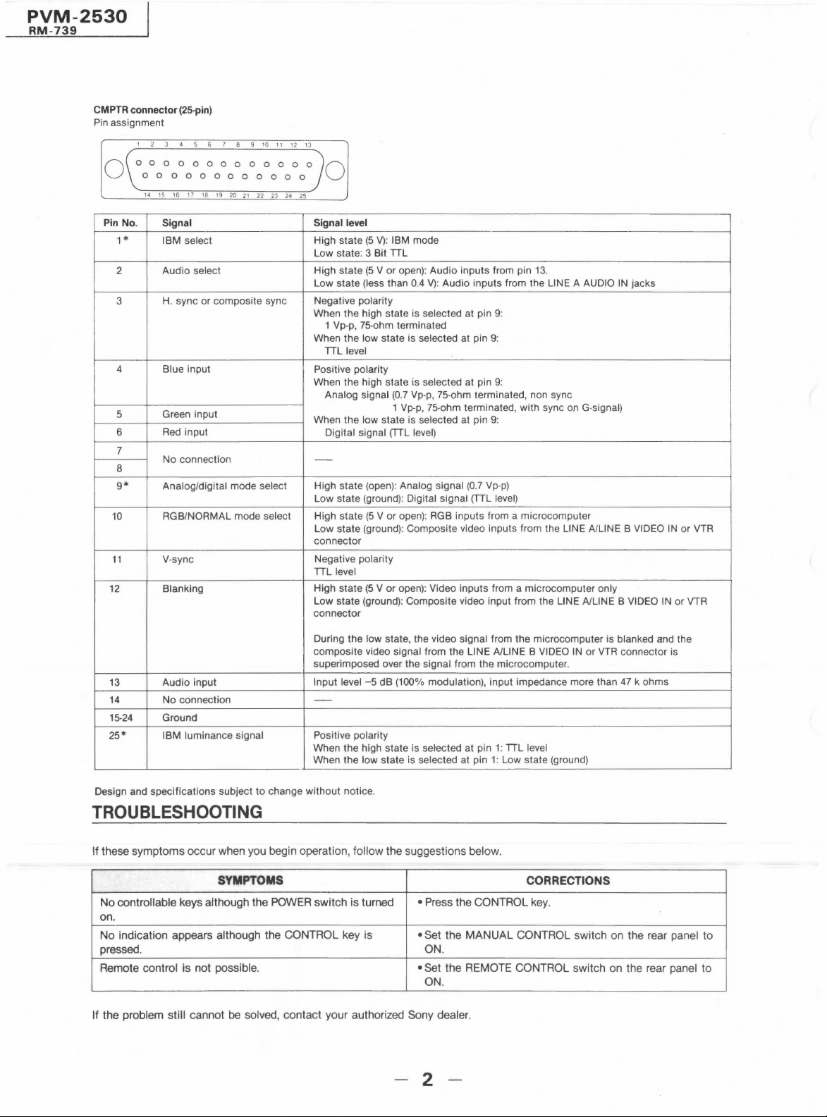
CM PTR connector (25-pin)
Pin assignment
0
1 2 3 4 5 6 7 8 9 10 11 12 13
0 0 0 0 0 0 0 0 0 0 0 O 0
0 0 0 0 0 0 0 0 0 0 0 O
14 15 16 17 18 19 20 2 1 22 23 24 25
0
Pin No.
1*
2
3
4 Blue input
5 Green input
6
7
8
9*
10
11 V-sync
12 Blanking
Signal
IBM select
Audio select
H. sync or composite sync
Red input
No connection
Analog/digital mode select
RGB/NORMAL mode select
Signal level
High state (5 V): IBM mode
Low state: 3 Bit TTL
High state (5 V or open): Audio inputs from pin 13.
Low state (less than 0.4 V): Audio inputs from the LINE A AUDIO IN jacks
Negative polarity
When the high state is selected at pin 9:
1 Vp-p, 75-ohm terminated
When the low state is selected at pin 9:
TTL level
Positive polarity
When the high state is selected at pin 9:
Analog signal (0.7 Vp-p, 75-ohm terminated, non sync
1 Vp-p, 75-ohm terminated, with sync on G-signal)
When the low state is selected at pin 9:
Digital signal (TTL level)
-
High state (open): Analog signal (0.7 Vp-p)
Low state (ground): Digital signal (TTL level)
High state (5 V or open): RGB inputs from a microcomputer
Low state (ground): Composite video inputs from the LINE A/LINE B VIDEO IN or VTR
connector
Negative polarity
TTL level
High state (5 V or open): Video inputs from a microcomputer only
Low state (ground): Composite video input from the LINE A/LINE B VIDEO IN or VTR
connector
During the low state, the video signal from the microcomputer is blanked and the
composite video signal from the LINE A/LINE B VIDEO IN or VTR connector is
superimposed over the signal from the microcomputer .
13 Audio input
14
15-24 Ground
25*
Design and specifications subject to change without notice.
No connection
IBM luminance signal
Input level -5 dB (100% modulation), input impedance more than 47 k ohms
-
Positive polarity
When the high state is selected at pin 1: TTL level
When the low state is selected at pin 1: Low state (ground)
TROUBLESHOOTING
If these symptoms occur when you begin operation, follow the suggestions below.
SYMPTOMS
No controllable keys although the POWER switch is turned
on.
No indication appears although the CONTROL key is
pressed.
Remote control is not possible. • Set the REMOTE CONTROL switch on the rear panel to
If the problem still cannot be solved, contact your authorized Sony dealer.
• Press the CONTROL key.
• Set the MANUAL CONTROL switch on the rear panel to
ON.
ON.
CORRECTIONS
2
SAFETY CHECK-OUT
(US model only)
After correcting the original service problem, LEAKAGE TEST
perform the following safety checks before releasing
the set to the customer:
Check the area of your repair for unsoldered or
l.
poorly-soldered connections. Check the entire
board surface for solder splashes and bridges.
Check the interboard wiring to ensure that no
2.
wires art "pinched" or contact high-wattage
resistors.
3. Check that all control knobs, shields, covers,
ground straps, and mounting hardware have
been replaced. Be absolutely certain that you
have replaced all the insulators.
4. Look for unauthorized replacement parts, particularly transistors, that were installed during a
previous repair. Point them out to the customer
and recommend their replacement.
5. Look for parts which, though functioning, show
obvious signs of deterioration. Point them out
to the customer and recommend their replacement.
6. Check the line cord for cracks and abrasion.
Recommend the replacement of any such line
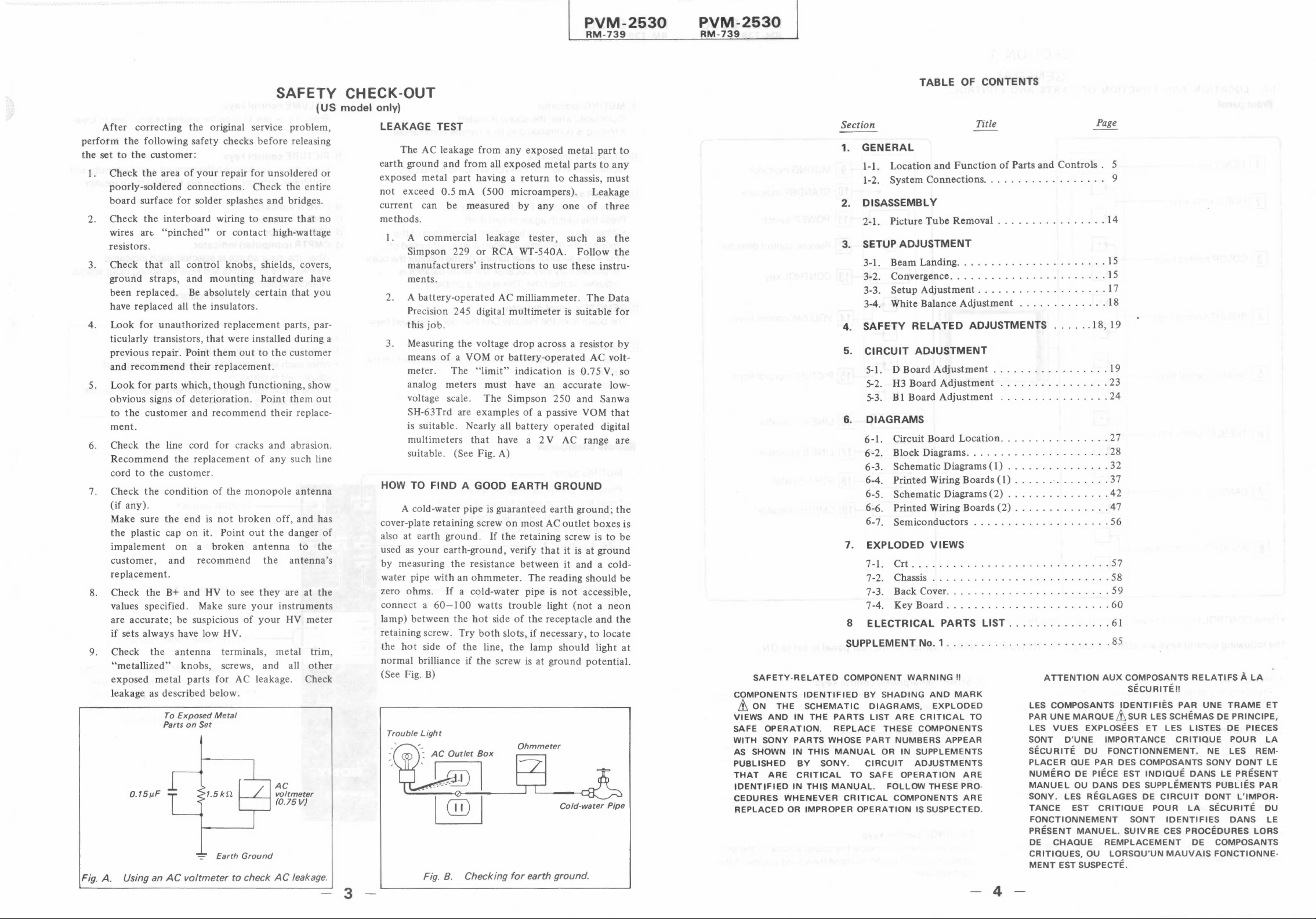
The AC leakage from any exposed metal part to
earth ground and from all exposed metal parts to any
exposed metal part having a return to chassis, must
not exceed 0.5 mA (500 microampers). Leakage
current can be measured by any one of three
methods.
I . A commercial leakage tester, such as the
Simpson 229 or RCA WT-540A. Follow the
manufacturers' instructions to use these instruments.
2. A battery-operated AC milliammeter. The Data
Precision 245 digital multimeter is suitable for
this job.
3. Measuring the voltage drop across a resistor by
means of a VOM or battery-operated AC voltmeter. The "limit" indication is 0.75 V, so
analog meters must have an accurate lowvoltage scale. The Simpson 250 and Sanwa
SH-63Trd are examples of a passive VOM that
is suitable. Nearly all battery operated digital
multimeters that have a 2 V AC range are
suitable. (See Fig. A)
cord to the customer.
7. Check the condition of the monopole antenna
(if any).
Make sure the end is not broken off, and has
the plastic cap on it. Point out the danger of
impalement on a broken antenna to the
customer, and recommend the antenna's
replacement.
8. Check the B+ and HV to see they are at the
values specified. Make sure your instruments
are accurate; be suspicious of your HV meter
if sets always have low HV.
9. Check the antenna terminals, metal trim,
"metallized" knobs, screws, and all other
exposed metal parts for AC leakage. Check
HOW TO FIND A GOOD EARTH GROUND
A cold-water pipe is guaranteed earth ground; the
cover-plate retaining screw on most AC outlet boxes is
also at earth ground. If the retaining screw is to be
used as your earth-ground, verify that it is at ground
by measuring the resistance between it and a coldwater pipe with an ohmmeter. The reading should be
zero ohms. If a cold-water pipe is not accessible,
connect a 60-100 watts trouble light (not a neon
lamp) between the hot side of the receptacle and the
retaining screw. Try both slots, if necessary, to locate
the hot side of the line, the lamp should light at
normal brilliance if the screw is at ground potential.
(See Fig. B)
leakag~ as described below.
To Exposed Metal
0.15µF
Parts on Set
1.5 kD.
AC
voltmeter
(0.15V)
Trouble Light
-=- Earth Ground
Fig. A. Using an AC voltmeter to check AC leakage.
3
-: AC Outlet Box
Fig. 8. Checking for earth ground.
Ohmmeter
Cold-water Pipe
PVM-2530
RM-739
PVM-2530
RM-739
SAFETY-RELATED COMPONENT WARNING!! ATTENTION AUX COMPOSANTS RELATIFS A LA
COMPONENTS IDENTIFIED BY SHADING AND MARK
& ON THE SCHEMATIC DIAGRAMS, EXPLODED
VIEWS AND IN THE PARTS LIST ARE CRITICAL TO
SAFE OPERATION. REPLACE THESE COMPONENTS
WITH SONY PARTS WHOSE PART NUMBERS APPEAR
AS SHOWN IN THIS MANUAL OR IN SUPPLEMENTS
PUBLISHED BY SONY. CIRCUIT ADJUSTMENTS
THAT ARE CRITICAL TO SAFE OPERATION ARE
IDENTIFIED IN THIS MANUAL. FOLLOW THESE PROCEDURES WHENEVER CRITICAL COMPONENTS ARE
REPLACED OR IMPROPER OPERATION IS SUSPECTED.
TABLE OF CONTENTS
Section
Title
1. GENERAL
1-1. Location and Function of Parts and Controls . 5
1-2. System Connections. . . . . . . . . . . . . . . . . . 9
2. DISASSEMBLY
2-1. Picture Tu be Removal . . . . . . . . . . . . . . . . 14
3. SETUP ADJUSTMENT
3-1. Beam Landing ...................... 15
3-2. Convergence ....................... 15
3-3. Setup Adjustment ................... 1 7
3-4. White Balance Adjustment ............. 18
4. SAFETY RELATED ADJUSTMENTS ...... 18, 19
5. CIRCUIT ADJUSTMENT
5-1. D Board Adjustment ................. 19
5-2. H3 Board Adjustment ................ 23
5-3. B 1 Board Adjustment ................ 24
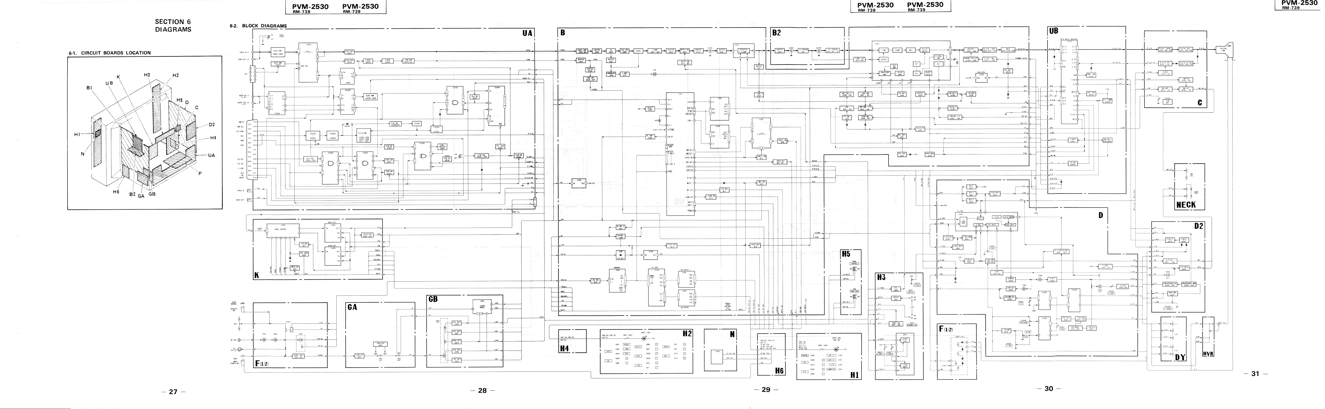
6. DIAGRAMS
6-1. Circuit Board Location ................ 27
6-2. Block Diagrams ..................... 28
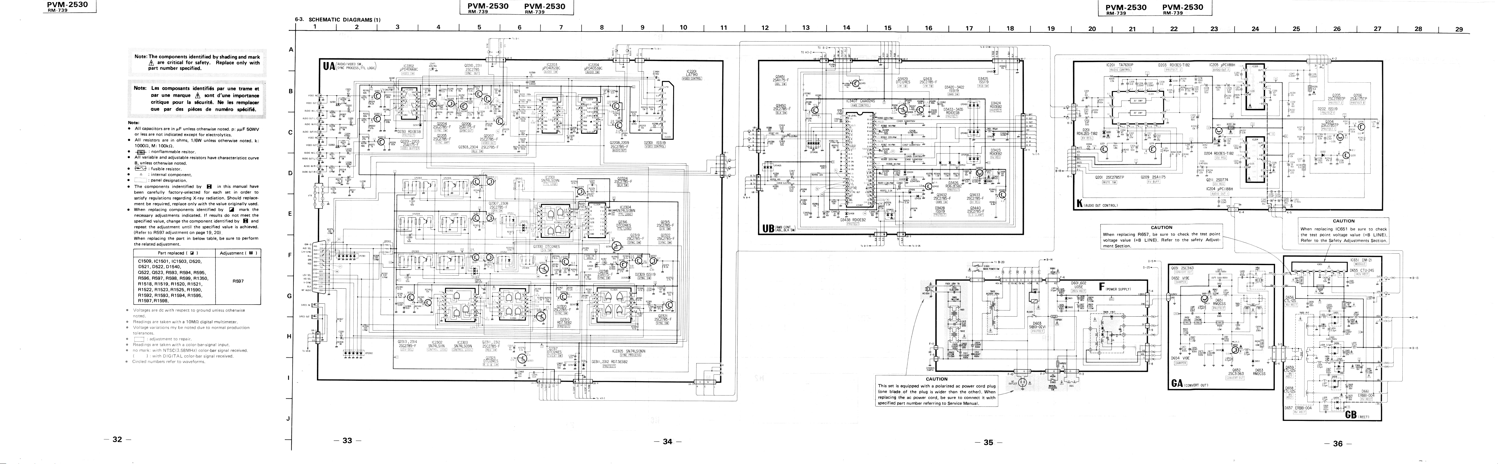
6-3. Schematic Diagrams (1) ............... 32
6-4. Printed Wiring Boards (1) .............. 37
6-5. Schematic Diagrams (2) ............... 42
6-6. Printed Wiring Boards (2) .............. 47
6-7. Semiconductors .................... 56
7. EXPLODED VIEWS
7-1. Crt ............................. 57
7-2. Chassis .......................... 58
7-3. Back Cover ........................ 59
7-4. Key Board ........................ 60
8 ELECTRICAL PARTS LIST . .............. 61
SUPPLEMENT No. 1 ........................ 85
LES COMPOSANTS IDENTIFIES PAR UNE TRAME ET
PAR UNE MARQUE &suR LES SCHEMAS DE PRINCIPE,
LES VUES EXPLOSEES ET LES LISTES DE PIECES
SONT D'UNE IMPORTANCE CRITIQUE POUR LA
SECURITE DU FONCTIONNEMENT. NE LES REMPLACER QUE PAR DES COMPOSANTS SONY DONT LE
NUMERO DE PIECE EST INDIQUE DANS LE PRESENT
MANUEL OU DANS DES SUPPLEMENTS PUBLIES PAR
SONY. LES REGLAGES DE CIRCUIT DONT L'IMPORTANCE EST CRITIQUE POUR LA SECURITE DU
FONCTIONNEMENT SONT IDENTIFIES DANS LE
PRESENT MANUEL. SUIVRE CES PROCEDURES LORS
DE CHAQUE REMPLACEMENT DE COMPOSANTS
CRITIQUES, OU LORSQU'UN MAUVAIS FONCTIONNEMENT EST SUSPECTE.
4
SECURITEI!
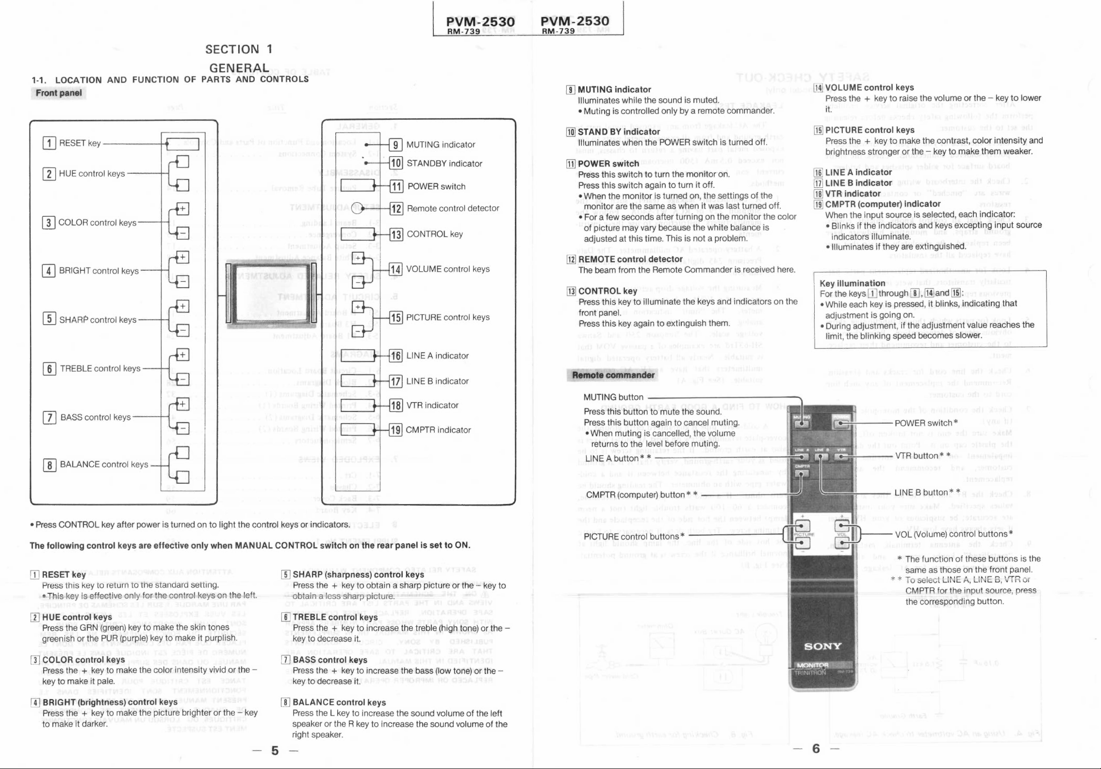
SECTION 1
GENERAL
1-1. LOCATION AND FUNCTION OF PARTS AND CONTROLS
Front panel
PVM-2530
RM-739
PVM-2530
RM-739
!I] MUTING indicator
Illuminates while the sound is muted.
• Muting is controlled only by a remote commander.
lM] VOLUME control keys
Press the + key to raise the volume or the - key to lower
it.
ITJ RESET key ------4 ...
....._ _ ___,
[I] HUE control keys--- ......
[I] COLOR control keys---
[I] BRIGHT control keys ---+---1
[[] SHARP control keys ---+-c
[[] TREBLE control keys
[]] BASS control keys ---
[[] BALANCE control keys
MUTING indicator
STANDBY indicator
POWER switch
Remote control detector
CONTROL key
LINE A indicator
LINE B indicator
VTR indicator
CMPTR indicator
[1ID STAND BY indicator
Illuminates when the POWER switch is turned off.
[I] POWER switch
Press this switch to turn the monitor on.
Press this switch again to turn it off
• When the monitor is turned on, the settings of tihe
monitor are the same as when it was last turned off.
•Fora few seconds after turning on the monitor the color
of picture may vary because the white balance is
adjusted at this time. This is not a problem.
[11] REMOTE control detector
The beam from the Remote Commander is received here.
[ill CONTROL key
Press this key to illuminate the keys and indicators on the
front panel.
Press this key again to extinguish them.
Remote commander
MUTING button ------ ------ -- -..
Press this button to mute the sound.
Press this button again to cancel muting.
• When muting is cancelled, the volume
returns to the level before muting.
LINE A button* * ____________ ...,,.._;
[fil PICTURE control keys
Press the + key to make the contrast, color intensity and
brightness stronger or the - key to make them weaker.
ml LINE A indicator
[j] LINE B indicator
[ID VTR indicator
rn] CMPTR (computer) indicator
When the input source is selected, each indicator:
• Blinks if the indicators and keys excepting input source
indicators illuminate.
• Illuminates if they are extinguished.
Key illumination
For the keys[]] through[[],~ and~:
• While each key is pressed, it blinks, indicating that
adjustment is going on.
• During adjustment, if the adjustment value reaches the
limit, the blinking speed becomes slower.
VTR button * *
• Press CONTROL key after power is turned on to light the control keys or indicators.
The following control keys are effective only when MANUAL CONTROL switch on the rear panel is set to ON.
OJ RESET key
ress this Key to return to me stanaara setting.
• This key is effective only for the control keys on the left.
[I] HUE control keys
Press the GRN (green) key to make the skin tones
greenish or the PUR (purple) key to make it purplish.
[I] COLOR control keys
Press the + key to make the color intensity vivid or the key to make it pale.
[I] BRIGHT (brightness) control keys
Press the + key to make the picture brighter or the - key
to make it darker.
[[] SHARP (sharpness) control keys
Press the + key to obtain a sharp picture or the - key to
obtain a less sharp picture.
[I] TREBLE control keys
Press the + key to increase the treble (high tone) or the key to decrease it.
[I] BASS control keys
Press the + key to ,increase the bass (low tone) or the -
key to decrease it.
[[] BALANCE control keys
Press the L key to increase the sound volume of the lleft
speaker or the R key to increase the sound volume of the
right speaker.
- 5
CMPTR (computer) button* * -- ---------..
PICTURE control buttons* ---------t
LINE B button**
* The function of these buttons is the
same as those on the front panel.
CMPTR for the input source, press
the corresponding button .
- 6
PVM-2530
RM - 739
PVM-2530
RM-739
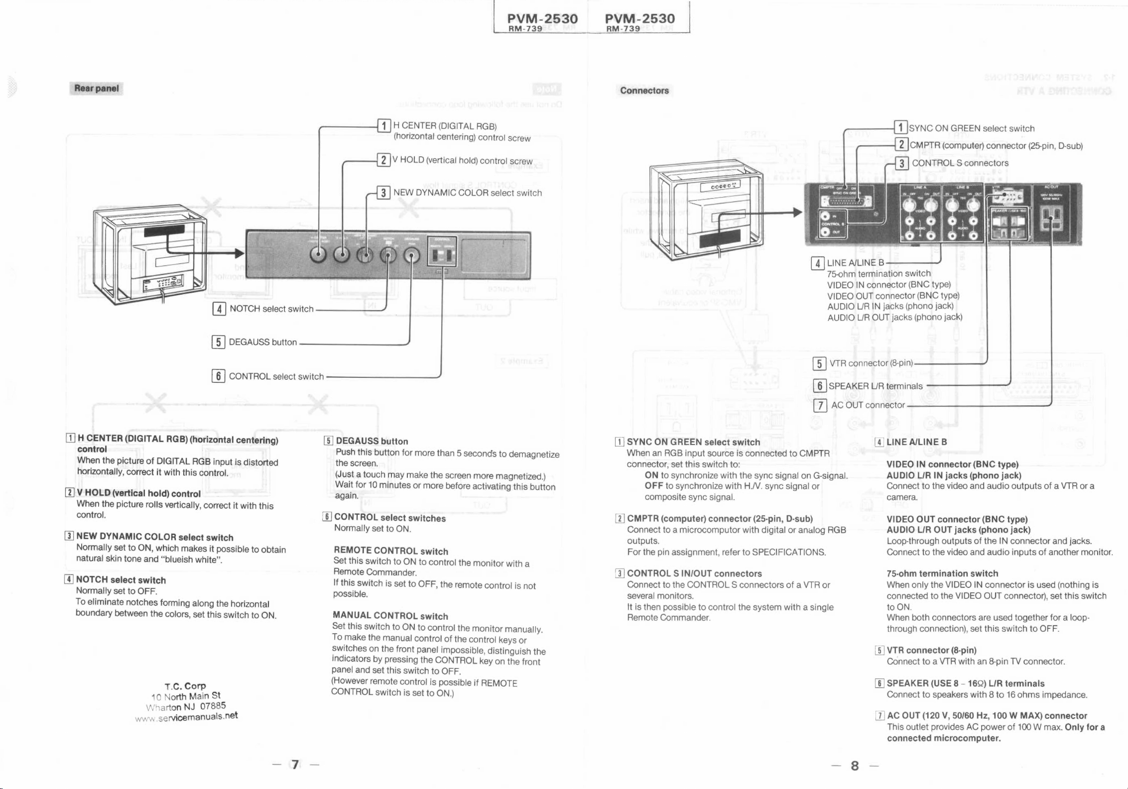
Rear panel
~----1 1 H CENTER (DIGITAL RGB)
(horizontal centering) control screw
-----ii 2 V HOLD (vertical hold) control screw
IT] NOTCH select switch ----~ -
(I] DEGAUSS button_ .......,_.._. _____ _
(]] CONTROL select switch------ ----
Connectors
SYNC ON GREEN select switch
CMPTR (computer) connector (25-pin, D-sub)
CONTROLS connectors
[I) LINE A/LINE B-- --
75-ohm termination switch
VIDEO IN connector (BNC type)
VIDEO OUT connector (BNC type)
AUDIO UR IN jacks (phono jack)
AUDIO UR OUT jacks (phono jack)
(]] VTR connector (8-pin)-------
[I) SPEAKER UR terminals -- -----
[TI H CENTER (DIGITAL RGB) (horizontal centering)
control
When the picture of DIGIT AL RGB input is distorted
horizontally, correct it with this control.
[I] V HOLD (vertical hold) control
When the picture rolls vertically, correct it with this
control.
[I] NEW DYNAMIC COLOR select switch
Normally set to ON, which makes it possible to obtain
natural skin tone and "blueish white".
[I] NOTCH select switch
Normally set to OFF.
To eliminate notches forming along the horizontal
boundary between the colors, set this switch to ON.
T.C. Corp
1 o North Main St
Wharton NJ 07885
wv.v. .servicemanuals.net
W DEGAUSS button
Push this button for more than 5 seconds to demagnetize
the screen.
(Just a touch may make the screen more magnetized.)
Wait for 10 minutes or more before activating this button
again.
[[] CONTROL select switches
Normally set to ON.
REMOTE CONTROL switch
Set this switch to ON to control the monitor with a
Remote Commander.
If this switch is set to OFF, the remote control is not
possible.
MANUAL CONTROL switch
Set this switch to ON to control the monitor manually.
To make the manual control of the control keys or
switches on the front panel impossible , distinguish the
indicators by pressing the CONTROL key on the front
panel and set this switch to OFF.
(However remote control is possible if REMOTE
CONTROL switch is set to ON.)
[]] AC OUT connector- ------ -- - ---
[I] SYNC ON GREEN select switch
When an RGB input source is connected to CMPTR
connector, set this switch to:
ON to synchronize with the sync signal on G-signal.
OFF to synchronize with H.N . sync signal or
composite sync signal.
[I] CMPTR (computer) connector (25-pin, D-sub)
Connect to a microcomputor with digital or analog RGB
outputs.
For the pin assignment , refer to SPECIFICATIONS.
[I] CONTROLS IN/OUT connectors
Connect to the CONTROLS connectors of a VTR or
several monitors.
It is then possible to control the system with a single
Remote Commander.
[I] LINE A/LINE B
VIDEO l'N connector (BNC type)
AU DIO L/R IN jacks (phono jack)
Connect to the video and audio outputs of a VTR or a
camera.
VIDEO OUT connector (BNC type)
AUDIO L/R OUT jacks (phono jack)
Loop-through outputs of the IN connector and jacks.
Connect to the video and audio inputs of another monitor.
75-ohm termination switch
When only the VIDEO IN connector is used (nothing is
connected to the VIDEO OUT connector), set this switch
to ON.
When both connectors are used together for a loopthrough connection), set this switch to OFF.
W VTR connector (8-pin)
Connect to a VTR with an 8-pin TV connector.
[[] SPEAKER (USE 8 - 16Q) L/R terminals
Connect to speakers with 8 to 16 ohms impedance.
DJ AC OUT (120 V, 50/60 Hz, 100 W MAX) connector
This outlet provides AC power of 100 W max. Only for a
connected microcomputer.
- 7
- 8
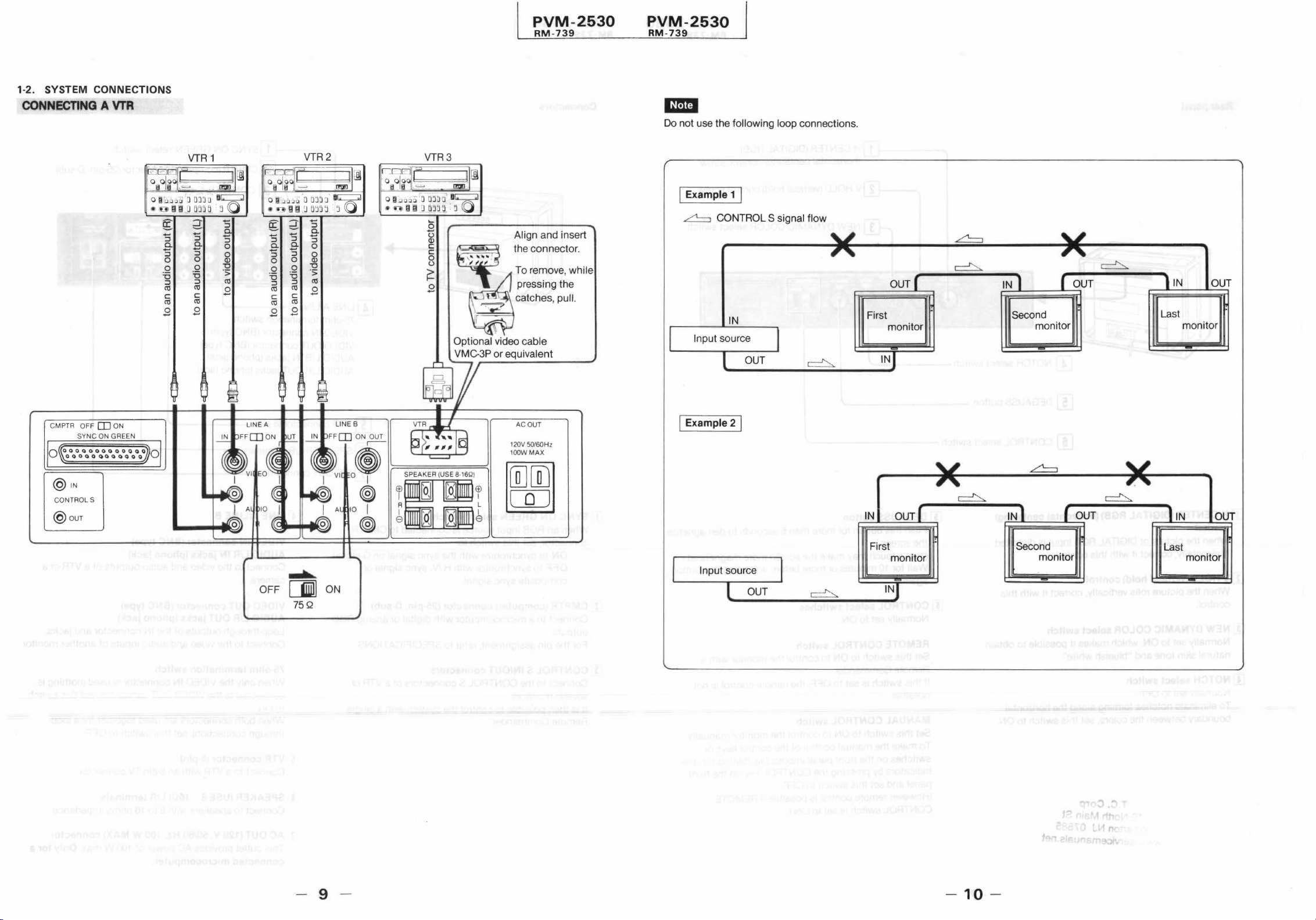
1-2. SYSTEM CONNECTIONS
CONNECTING A VTR
PVM-2530
RM-739
PVM-2530
RM-739
Do not use the following loop connections.
pa-rn
t_i! !'I L~ -- - - __cm;J_
CMPTR OFF DJ ON
SYNC ON GREEN
0 00000000000~0000000000000 0
@1N
CONTROLS
@ouT
VTR 1
= J
1
O~ - - --
o ~61>.oli 'a n:i~ a· a~
u~ n ~o a_~na_ 5 0
g
:5
Cl.
:5
0
0
u
::::,
(,;l
C
(,;l
.8
2
:5
Cl.
:5
0 (1)
0
u
::::,
(,;l
C
(,;l
.8
:5
Cl.
:5
0
0
-0
·5=
(,;l
.8
~
a:
:5
Cl.
:5
0
0
u
::::,
(,;l
C
(,;l
.8
2
:5
Cl.
:5
0
0
u
(,;l
C
(,;l
.8
::::,
VTR2
:5
Cl.
:5
0
0
(1)
-0
·5=
(,;l
.8
IN
LINE B
FF[D ON OUT
,--
~
o I
~
A
10
I
(®)
VTR3
0
u
(1)
C
C
0
(.)
~
.8
SPEAKER (USE 8-16Q )
(f)
I
R
I
e
Align and insert
the connector.
, .. " --
~
I I
To remove, while
pressing the
catches, pull.
.
-
Optional video cable
_VMC-3P or equivalent
AC OUT
120V 50/60Hz
100W MAX
(f)
I
L
UlJ
~
I
e
I Example 1 I
~--=:J CONTROL S signal flow
IN
Input source
I Example 21
OUT
First
monitor
IN
IN. OUT
IN OUT
Second
monitor
IN
OUT
IN OUT
......
OFF []Im] ON
75Q
Input source
OUT
c::.~
First
monitor ,
Second
monitor
Last
monitor
- 9
- 10 -
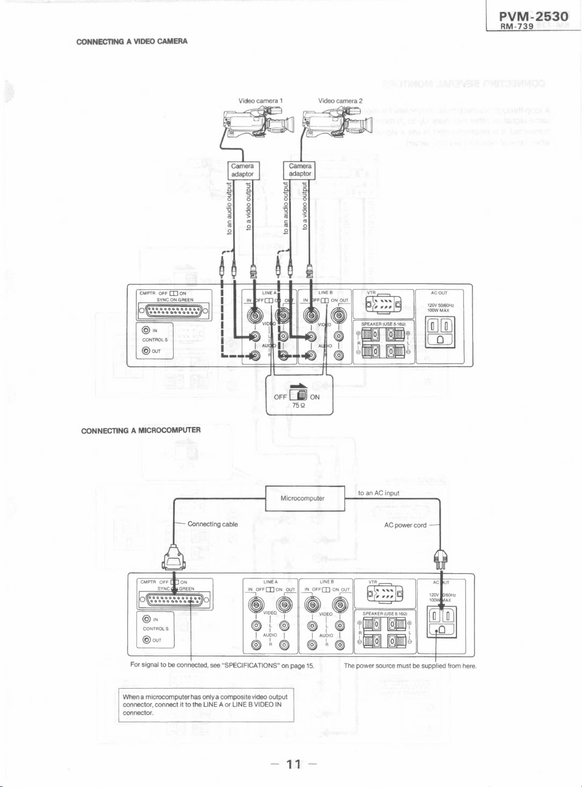
CONNECTING A VIDEO CAMERA
Video camera 1 Video camera 2
Camera
adaptor
'S
0..
'S 'S
0
Q.
'6
::,
<1:1 ">
C
<1:1
.8
'S
0..
0
2
"O
<1:1
.8
'S
0..
'S
'S
0
0
0
2
ii
"O
::,
">
<1:1
<1:1
C
<1:1
.8
.8
PVM-2530
RM-739
CMPTR OFF [I) ON
@1N
CONTROLS
@our
CONNECTING A MICROCOMPUTER
Connecting cable
IN
......
OFF []I ON
75Q
Microcomputer
LINE B
FF[I] ON OUT
,---
e
o I
~
A 10 I
~
AC OUT
120V 50/60Hz
~
-
SPEAKER (USE 8-16Q)
I ' ' I
R L
I
~
e , O e
·u·
@J I
to an AC input
AC power cord
lOOWMAX
~
0
LINEA
~OFF[I)ON~
eVIDEOe
@1N
CONTROLS
@our
For signal to be connected, see "SPECIFICATIONS" on page 15.
When a microcomputer has only a composite video output
connector, connect it to the LINE A or LINE B VIDEO IN
connector.
I I I
®~@
I AUDIO I
@) ~@
- 11
LINE B
IN OFF [I] ON OUT
--, ,---
~
~IDEOe
I I I
@~~
I AUDIO I
@~~
SPEAKER (USE 8-16Q)
I ' ' I
A L
I
~
8 , 0 8
·n·
The power source must be supplied from here.
-
@J I
PVM-2530
RM-739
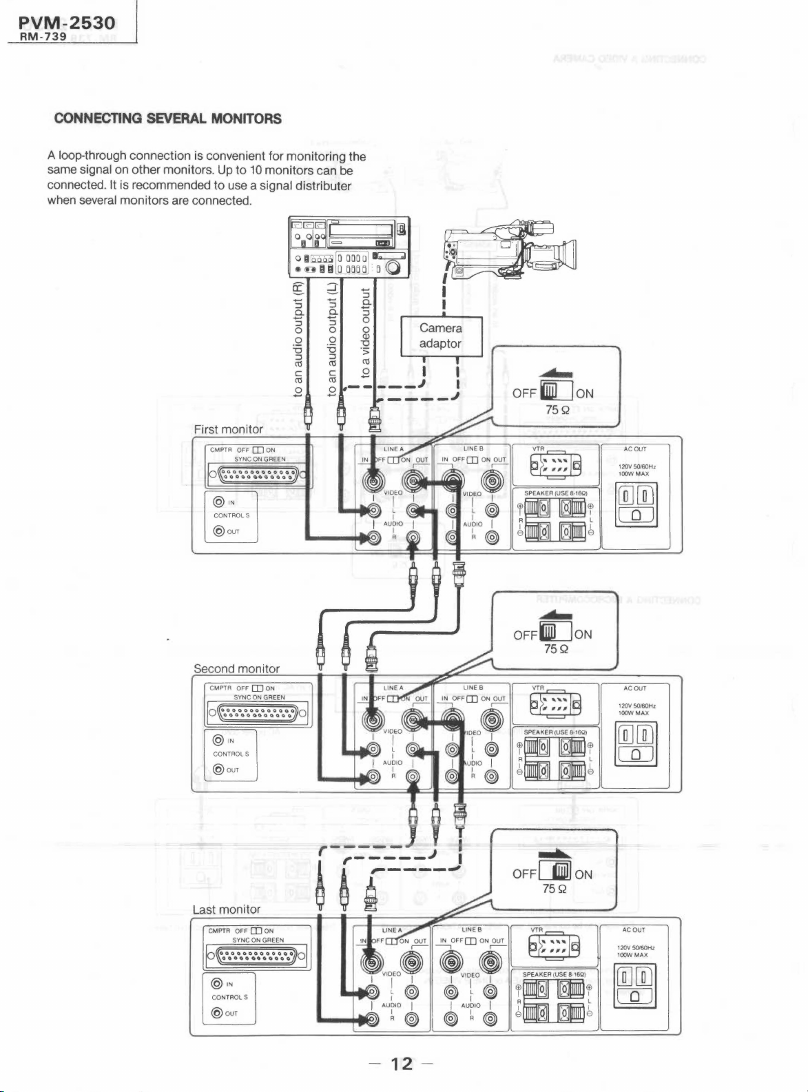
CONNECTING SEVERAL MONITORS
A loop-through connection is convenient for monitoring the
same signal on other monitors. Up to 10 monitors can be
connected. It is recommended to use a signal distributer
when several monitors are connected.
rf_
:5
Q.
:5
0
.Q
"O
:::,
CTl
First monitor
CMPTR OFF [I) ON
SYNC ON GREEN
O OOOOOOOOOOOQQ
OOOOOQiOOOOOO
@1N
CONTROLS
@our
2
:5
Q.
:5
0 0
.Q
"O
:::,
CTl
C
CTl
,--
.8
:5
Q.
:5
0
Q)
"O
·;;:
CTl
.8
___ J I
Camera
adaptor
----.I
IN OFF(I] ON OUT
--, ,----
,mrn~
I
~~
AUDIO I
~
~
......
OFFL]ON
75Q
AC OUT
[I]
~
120V 50160Hz
100WMAX
I
,
§9
SPEAKER (USE 8-16Q)
I ' , I
·1@11,·
r @J @J
e , O e
Second monitor
CMPTR OFF [I) ON
SYNC ON GREEN
@ 1N
CONTROLS
@ ouT
Last monitor
CMPTR OFF [I) ON
SYNC ON GREEN
@1N
CONTROLS
@ouT
ON OUT
f
~
AUDIO I
"1'°'
~~
......
OFFlil[JON
75Q
--"'--, Off (D o, /"'- §9
mo~ I :==S=PE=AK=E=R =(U=~=a=. ,6=Q)=='.,/
f
~
U~IO
LINE B VTR
IN OFF [I] ON OUT
--, ,----
~IDEO e l::==SP=E=AK=E=R =(US=E=a.=,6=Q)===;
@> f ® rl@i :~1~
1 AUDIO I r
~~~
rl@i :, ~
~
! @] @J
..........
OFFDlIDJ ON
~
~
~
e
~&
75Q
~
~
~
e
AC OUT
120V 50/60Hz
HJ0WMAX
AC OUT
120V 50/60Hz
100WMAX
m :
l@ 1
- 12 -
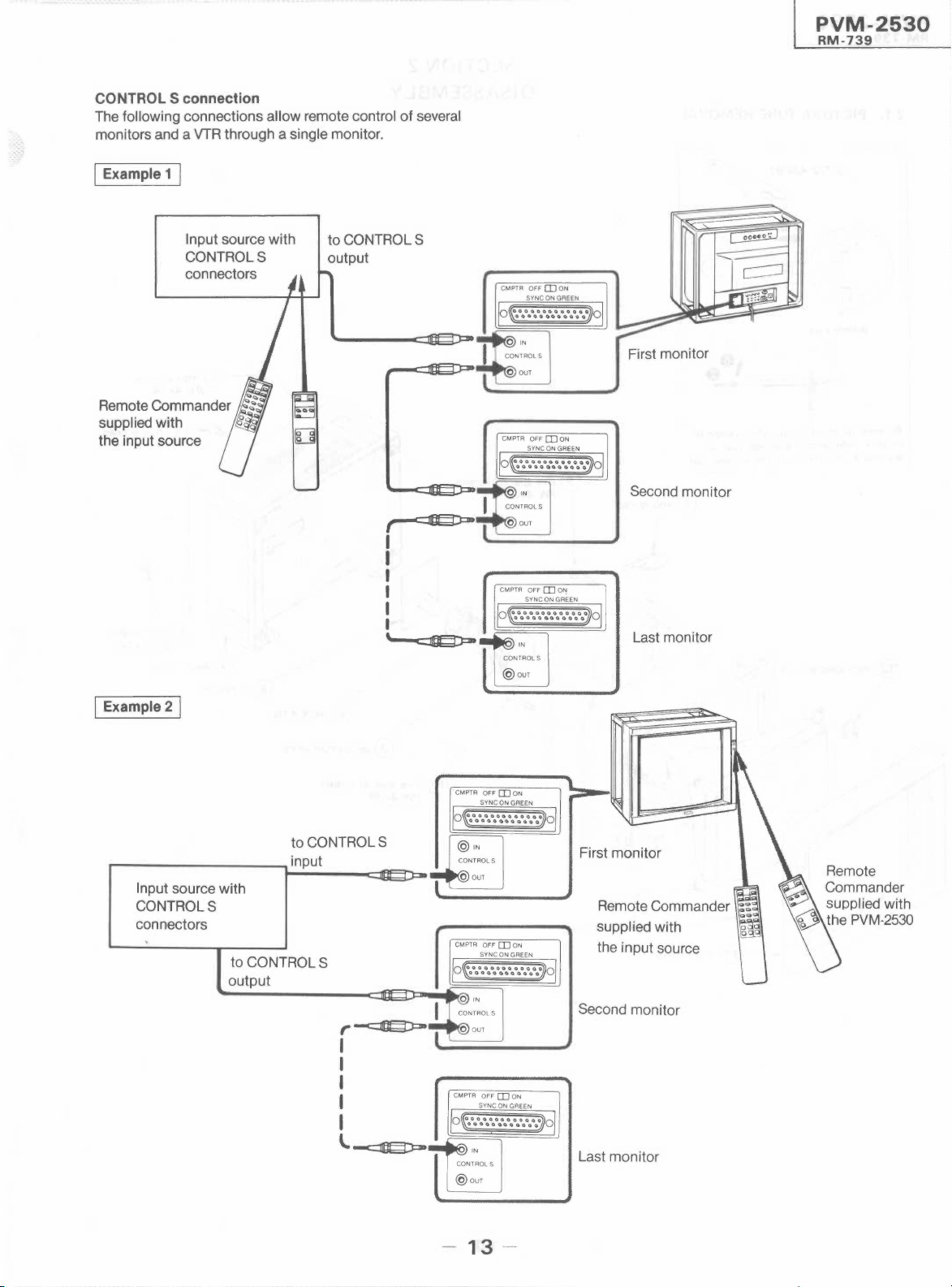
CONTROL S connection
The following connections allow remote control of several
monitors and a VTR through a single monitor.
Example 1
PVM-2530
RM-739
Input source with
CONTROLS
connectors
Remote Commander
supplied with
the input source
I Example 21
to CONTROLS
output
I
I
I
I
I
I
I
'
c...JlbbP=-
CMPTR OFF DJ ON
/o~ .... :::.:.:.:.:~::.: ·:J)oJ
First monitor
Second monitor
Last monitor
to CONTROLS
...... --- -- ---- --. input
Input source with
CONTROLS
connectors
to CONTROLS
output
t----==Jlfl;;D=-
r~
I
I
I
I
I
l ......:::Jiblbd
CMPTR OFF DJ ON
SYNC ON GREEN
CONTROLS
@our
- 13 --
First monitor
Remote Commander
supplied with
the input source
Second monitor
Last monitor
PVM-2530
RM-739
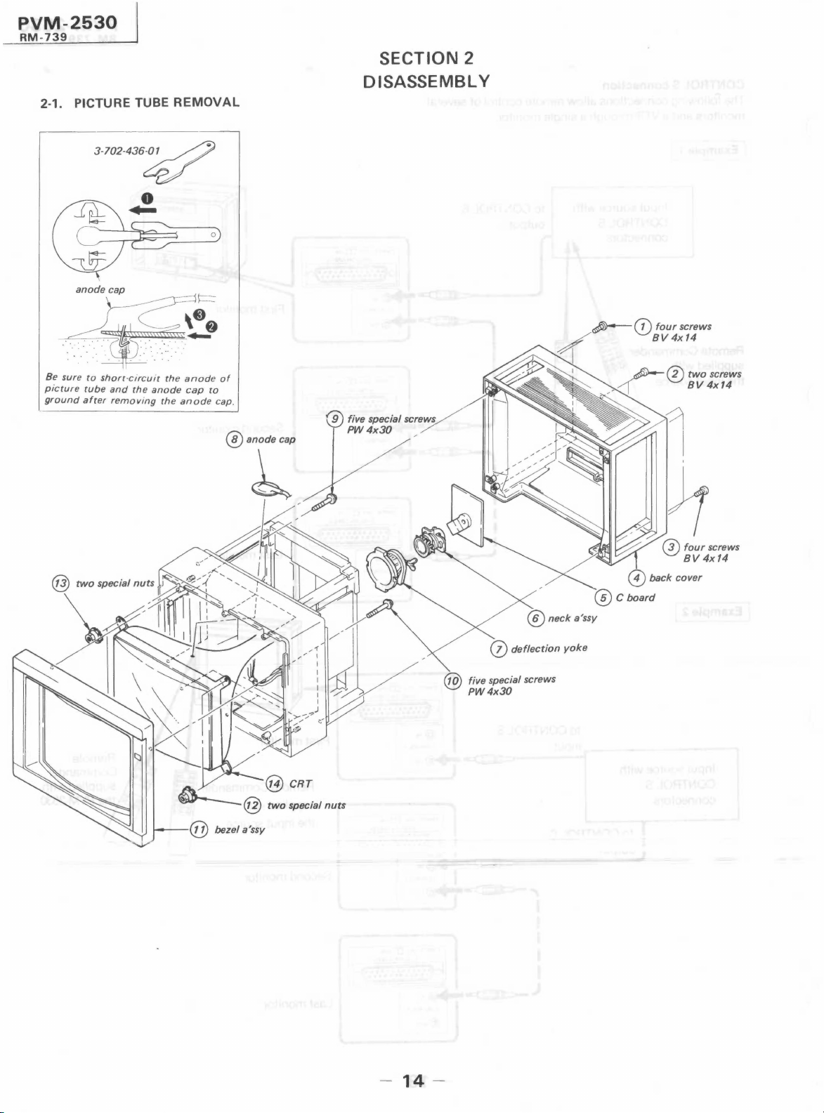
2-1. PICTURE TUBE REMOVAL
3-702·436~
Be sure to shorc-circuic the anode of
picture tube and the anode cap to
ground after removing the anode cap.
SECTION 2
DISASSEMBLY
five special screws
PW4x30
;--(}) four screws
/ BV4x14
I
~
_,(1 BV 4x14
® two screws
n
@necka'ssy
@cboard
1
@ four screws
BV 4x14
0 back cover
- 14 -
SECTION 3
SETUP ADJUSTMENTS
PVM-2530
RM-739
The following adjustments should be made when a complete
realignment is required or a new picture tube is installed.
These adjustments should be performed with rated power
supply voltage unless otherwise noted.
13-1. BEAM LANDING!
Preparation:
• Feed in the white pattern.
• Before starting, degauss the entire screen.
1. Loosen deflection yoke screw.
2. Position neck ass'y as shown in Fig. 3-1.
3. Adjust purity control as shown in Fig. 3-2.
4. Slide deflection yoke as far forward as it will
go.
5. Turn the raster signal of the pattern generator to
red.
6. Adjust purity control to center vertical red band
as shown in Fig. 3-3.
7. Slide deflection yoke back for a uniform red
screen.
8. Check green and blue rasters for uniformity by
performing the same way as steps 5 ,6 and 7.
9. Tighten the deflection yoke screw.
10. Check if mislandihg appears at corners a - d as
shown in Fig. 3-4. If mislanding is observed,
correct it as shown in Fig. 3-4.
11. Confirm that beam landing is correct when the
receiver is faced in all directions.
Perform the adjustments in order as follows:
1. Beam Landing
2. Convergence
3. SCREEN and White Balance
Note: Test Equipment Required.
1. Color-bar/Pattern Genertator
2. Degausser
I
I
I
Fig. 3-2.
i[p(qG~q
J '
G1 G3
Fig. 3-1.
Purity control corrects
this area.
BLUE
Disk magnets
or rotatable
disk magnets
correct these
areas (a-d).
GREEN
Fig. 3-3.
purity control
®
- 15 -
Deflection yoke positioning
corrects these areas.
Fig. 3-4.

PVM-2530
RM-739
jcoNVERGENcEI
Preparation:
• PICTURE ---i_ f ll . l k .
• BRIGHTNESSJ u y counterc oc w1Se
• CORNER BOW (RV2504)
• fl.TILT (RV2502)
• Y.BOW (RV2503)
• H.AMP (RV2501)
• Y.CROSS (RV2505)
• Input a dots signal.
1. Match the horizontal convergence at the center
of the screen with H.STAT VR.
2. Match the vertical convergence at the center of
the screen with V.STAT Mg.
D2 board
mechanical center
4. When the V.STAT magnet is moved in the direction of arrow a and b , Red, Green and
Blue dots move as shown below.
0 0 @
®I'\@ _:t!__ _:tL_
Rt t Rt t
0
I
T
@
@
/
/
/
I
R G B
V.STAT
magnet
RV706
SUBBRT
RV705
R. CUTOFF
--RV703
8. CUTOFF
screen
3. If the red, green and blue dots do not coincide
on the center of screen with H.ST AT VR, perform horizontal convergence adjustment using
H.STAT V~ and V.STAT magnet as shown
below.
(In this case, H.STAT VR and V.STAT magnet
effect each other.)
0
®
B'\_
@
G
'o
B
If blue dot does not coincide with red and green
dot, perform following steps.
Move BMC magnet (a) to correct insufficient H.
static convergence.
In either case, repeat Beam Landing Adjustment.
BMC magnet
G
!~~
. ,~
~
r
- 16 -
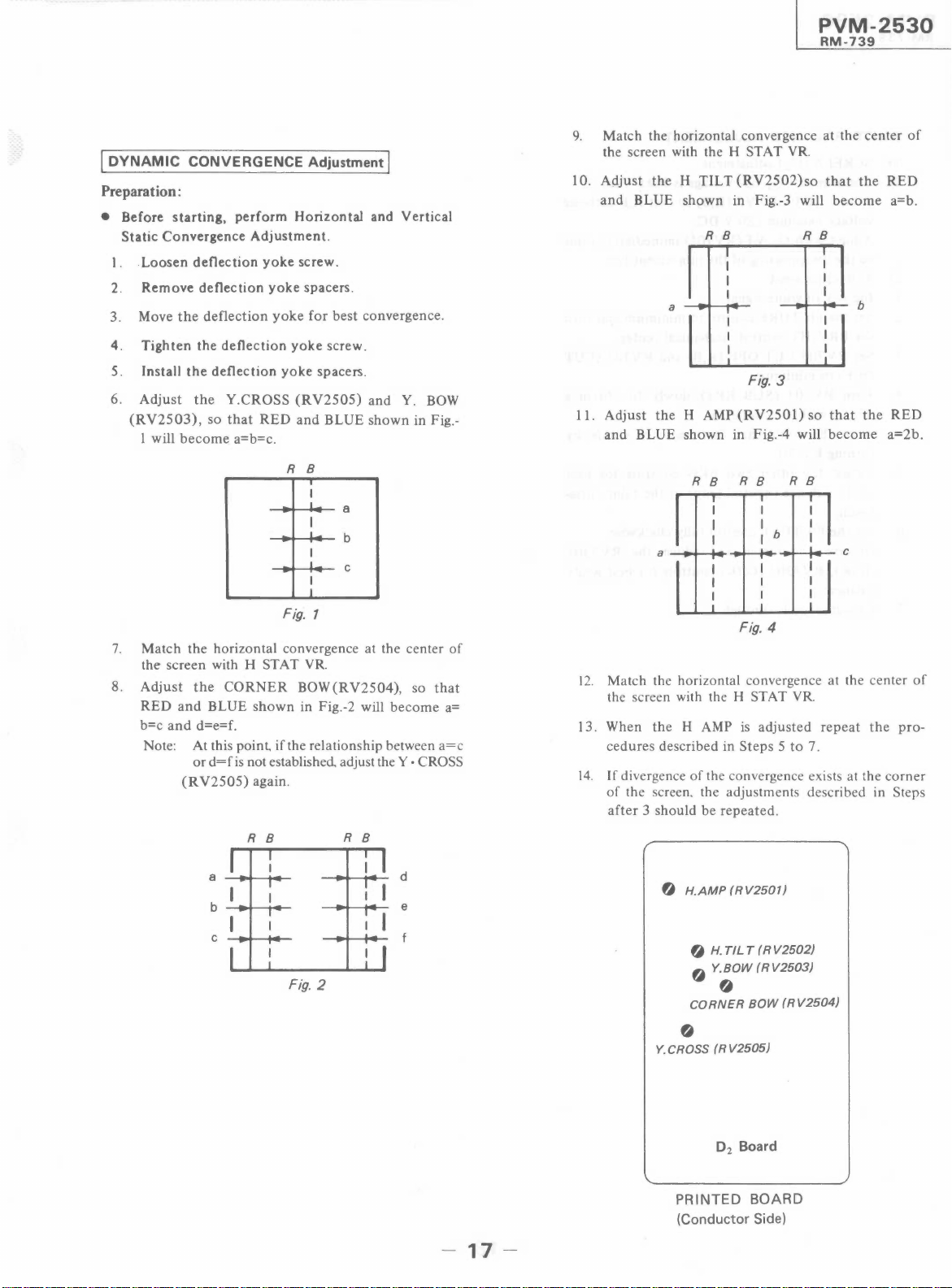
I DYNAMIC CONVERGENCE Adjustment I
Preparation:
• Before starting, perform Horizontal and Vertical
Static Convergence Adjustment.
l. Loosen deflection yoke screw.
2. Remove deflection yoke spacers.
3. Move the deflection yoke for best convergence.
4. Tighten the deflection yoke screw.
5. Install the deflection yoke spacers.
6. Adjust the Y.CROSS (RV2505) and Y. BOW
(RV2503), so that RED and BLUE shown in Fig.-
I will become a=b=c.
R 8
I
I
I
-
-
-
Fig. 1
7. Match the horizontal convergence at the center of
the screen with H ST AT YR
8. Adjust the CORNER BOW(RV2504), so that
RED and BLUE shown in Fig.-2 will become a=
b=c and d=e=f.
Note: At this point, if the relationship between a=c
or d=f is not established adjust the Y • CROSS
(RV2505) again.
R 8
a
I
I -
b
.
I
I
C
-
I
I
R B
PVM-2530
RM-739
9. Match the horizontal convergence at the center of
the screen with the H ST AT YR
10. Adjust the H TILT (RV2502)so that the RED
and BLUE shown in Fig.-3 will become a=b.
R 8 R 8
I
I
I
I
-
-
p
a
I -
I
I
I
I
Fig. 3
11. Adjust the H AMP (RV2501) so that the RED
and BLUE shown in Fig.-4 will become a=2b.
RB RB RB
b
Fig. 4
12. Match the horizontal convergence at the center of
the screen with the H ST AT YR
13. When the H AMP is adjusted repeat the pro-
cedures described in Steps 5 to 7.
14. If divergence of the convergence exists at the corner
of the screen. the adjustments described in Steps
after 3 should be repeated.
/
I
I
I
I
-
, -
-
b
I
I
I
I
Fig. 2
d
e
- 17 -
0 H.AMP (RV2501)
0 H. TILT (RV2502)
O Y. BOW ( R V2503)
0
CORNER BOW (RV2504)
0
Y.CROSS (RV2505)
D
Board
2
PRINTED BOARD
(Conductor Side)
_/

PVM-2530
RM-739
WHITE BALANCE ADJUSTMENT
1) SCREEN (G
1. Confirm that G
2. Adjust CUT OFF VR (R,B) so that R,B cathode
voltage becomes 180 V DC.
Adjust with G2 VT ( R V701) immediately prior
to the disappearing of the luminscent line.
2) W /B adjustment
1. Input a all white signal.
2. Set the PICTURE control to minimum and turn
the BRIGHT control mechanical center.
3. Set RV705 CUT OFF (R,B) and RV703 (CUT
OFF) to minimum.
4. Turn RV701 (SUB BRT) slowly to obtain a
faintly visible cross-hatch.
Note the color that first becomes visible by
turning R V701.
5. Adjust the other two BKG controls for best
white balance (neutral gray) of the faint corss-
hatch.
6. Set the rICTURE control fully clockwise .
Observe the screen and adjust the RV3301
(B ,IK), RV3302 (G,IK) controls for best white
balance.
7. Repeat steps 1, through 7.
) adjustment
2
line voltage is 30±5 Vdc.
1
- 18 -
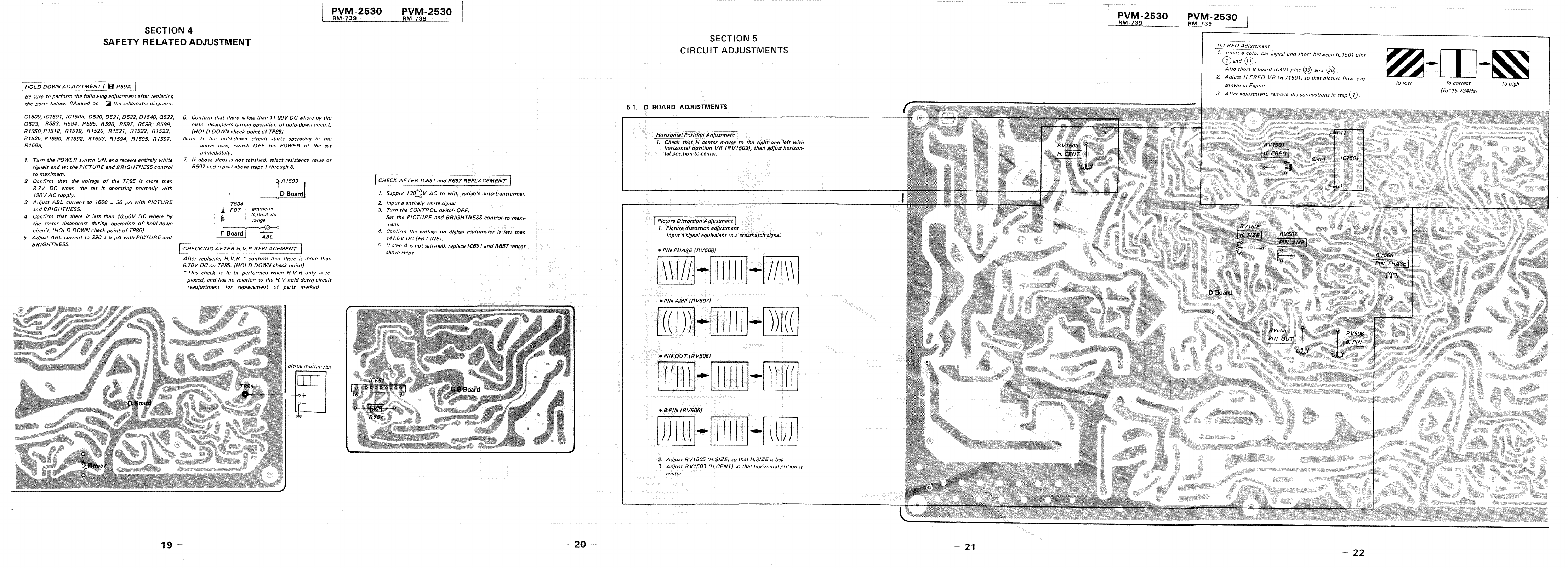
SECTION 4
SAFETY RELATED ADJUSTMENT
[H~LD DOWN ADJUSTMENT( 8 R591!l
Be sure to perform the fol/ow;ng adjustment after replacing
the parts below. (Mark.ed on C. the schematic diagramt
C1509, IC1501, IC1503, D520, D521, 0522, D1540, 0522,
0523, R593, R594, R595, R596, R597, R598, R599,
R1350,R1518, R/519, R/520, R/521, R1522, R1523,
R1525, R1590, R1592, R1593, R/594, R1595, R/597,
R/598,
1. Tum the POWER switch ON, and receive entirely white
signals and set the PICTURE and BRIGHTNESS control
to max imam.
2 Confirm that the voltage of the TP85 is more than
8. JV DC when the set is operr:1ting normally with
120V AC supply.
3. Adjust ABL current to 1600 ± 30 µA with PICTURE
and BRIGHTNESS.
4. Confirm that there is -less than 10.50V DC where by
the raster disappears during operation of hold-down
circuit. (HOLD DOWN check point of TP85)
5. Adjust ABL current to 290 ± 5 µA with PICTURE and
BRIGHTNESS.
6. Confirm that there is less than 11.00VDCwherebythe
raster disappears during operation of hold-down circuit.
(HOLD DOWN check point of TP85)
Note: If the hold·down circuit starts opera6ng in the
above case, switch OFF the POWER of the set
immediately.
7. If above steps is not satisfied, select resistance value of
R597 and repeat above steps 1 through 6.
R/593
-
ABL
D Board
'
'
:T604
: t :FBT
' '
' '
' '
L.~
~~J
F Board
ammeter
3.0mA de
range
I CHECKING AFTER H. VR REPLACEMENT
After replacing H. V. R * confirm that there is more than
8.70V DC on TP85. {HOLD DOWN check point)
* This check is to be performed when H. V. R only is re-
placed, and has no relation to the H. V hold-dawn circuit
readjustment for replacement of parts marked
PVM-2530
RM-739
PVM-2530
RM-739
CHECK AFTER /C65f and R657 REPLACEMENT
1. S1Jpp/v 13D~V AC to with variable auto-transformer.
2. Input a entirely white signal.
3. Turn the CONTROL switch OFF.
Set the PICTURE and BRIGHTNESS control to maxi-
mam.
4, Confirm the voltage an digital multimeter is less than
14L5V DC (+BLINE).
5. ff step 4 is not satisfied, replace IC651 and R657 repeat
above steps.
CIRCUIT ADJUSTMENTS
D BOARD ADJUSTMENTS
5-1.
! HorizOntaJ Position Adjust~_e_'!.~]
1. Check that H center moves to the right and left with
horizontal position VR (R V1503J~ then adjust horizontal position ta center.
] Picture Distortion Adjustment [
1. Picture distortion adjustment
Input a signal equivalent to a crosshatch signal.
• PIN PHASE (RV508}
~-..[[]]J]-[l@]
SECTION 5
···L- ~P=v'--'M=<--2_s_J_o _ _,_,P.,,_v_,_M,,_,,-'.._2_s_J_o__j
. RM-739 RM-739
f -H. FR ~9 XdJu;t;,;;n_{J
1. Input a color bar signal and short between IC1501 pins
(i)and@.
Also short B board IC401 pins@ and IJ§l.
2 Adjust H.FREQ VR (RV1501) so that picture flow isas
shown in Figure.
3. After adjustment, rernove the connections In step (0.
~-[[]-~
fo low
fo correct
(fo-15.734Hz)
fa high
ditital multimeter
{:: i 'I
• PIN AMP /RV507)
• PIN OUT (RV505)
[TIJ]J ... [ill]]-[illill
• /!.PIN (RV506)
2.. Adjust RV1505 (H.SJZE) so that H.SIZE is bes.
3. Adjust RV1503 (H.CENT) so that horizontal psitfon is
center.
- 19
20
- 21
- 22 -
PVM-2530
RM-739
PVM-2530
RM-739
PVM-2530
RM-739
PVM-2530
RM-739
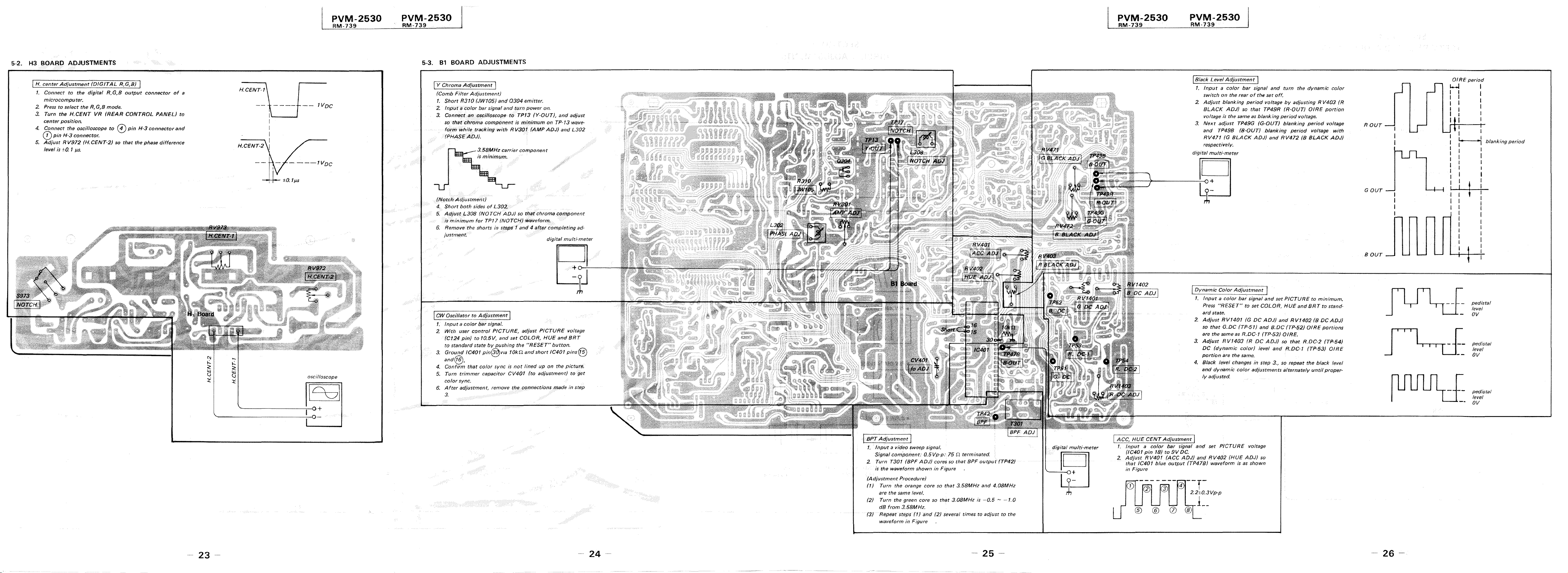
5-2. H3 BOARD ADJUSTMENTS
! H. center Adjustment (DIGITAL R,G,B)
1. Connect to the digitaf R,G,B output connector of a
microcomputer.
2 Press to select the R,G,B mode.
3_ Turn the H.CENT VR /REAR CONTROL PANEL} to
center position.
4. Connect the oscilloscope to © pin H-3 connector and
(j) pin H-3 connector.
5. Adjust R V972 (H.CENT-2) so that the phase difference
level is ±0. 1 µs.
H_CENT-2
----tvoc
±0. 1 µ.s
IVDc
5-3. Bl BOARD ADJUSTMENTS
! Y Chroma Adjustment I
(Comb Filter Adjustment)
1. Short R310 (JW105J and 0304 emitter.
2. Input a color bar signal and turn power on.
3. Connect ,E!n oscilloscope to TP13 (Y-OUTJ, and adjust
so that chroma compOnent is minimum on TP-13 wave-
fofm while tracking with RV301 (AMPAOJ) and L302
/PHASE ADJ).
-~~3.58MHz carrier component
/Notch Adjustmen-'i:)
4. Short both sides of L302..
5. Adjust L308 (NOTCH ADJ) so that chroma component
is minimum for TP17 (NOTCH) waveform,
6. Remove the shorts in stfJps' 1 and 4 a(ter completing ad-
justment
is minimum.
digital multi·meter
I Black Level Adjustment I
1. Input a color bar signal and turn the dynamic color
switch on the rear of the set off.
2 Adjust blanking period voltage by adjusting R V403 (R
BLACK ADJ) so that TP49R (R~OUTJ O!RE portion
voltage is the same as blanking period voltage.
3. Next adjust TP49G (G-OUT) blanking period voltage
and TP49B (B-OUT) blanking period voltage with
RV471 (G BLACK ADJ) and RV472 /B BLACK ADJ)
respectively.
digital multi-meter
ROUT
GOUT
BOUT
GIRE period
1-.J I
I
I
I
I
I
I
I
I
I, I
•1 blanking period
1
I
I
I
I
I
! I
~-------~--o+
oscilloscope
l°c7I
I CW Oscillator to Adjustment j
1. Input a color bar signal.
2 With user control PICTURE, adjust PICTURE voltage
(Ct 24 pin/ to 10.5V, and set COLOR, HUE and BRT
to standard state by pushing the "RESET"' button.
3, Ground JC401 pin@v1a 10ki1 and short IC401 pins@
and@. _ . .
4. Confirm that color sync Is not !med up on the p1cturf!,
5. Turn trimmer capacitor CV401 (to adjustment) to !}et
color sync.
6. After adjustment, remove the connections made in step
3.
1. Input a video sweep s1'.gnal.
Signal comPonent: 0.5Vp-p: 15 .11 terminated.
2. Turn T301 (SPF ADJ) cores so that BPF output (TP42J
is the waveform shown in Figure
(Adjustment Procedure)
(1) Turn the orange core so that 3.58MHz and 4.08MHz
are the same level.
(2) Turn the green core so that 3.08MHz is -0.5 - -1.0
dB from 3.58MHz.
(3) Repeat steps (1) tmd (2) several times to adjust to the
waveform in Figure
di'gitai multi"meter
ijJ
[ovf]a"mic Color Adjustment 1
1. Input a color ba( signal and set PICTURE to minimum.
Press "RESET" to set COLOR, HUE and BRT to stand-
ard state.
2. Adjust RV/401 /G DC ADJ) and RV/402 (B DC ADJ)
so that G.DC (TP-51) and B.DC (TP-52) DIRE portions
are the same as R.DC·1 (TP-53) 0/RE.
3, Adjust RV1403 (R DC ADJ) so that R.DC-2 (TP·54)
DC (dynamic color} level and R.DC-1 (TP-53} OIRE
portion are the same.
4, Black level changes in step 3., so repeat the black level
and dynamic color adjustments alternately until proper-
ly adjus(ed.
I ACC, HUE CENT Adjustment I
1. Input a color bar ,;ignal and set PICTURE voltage
/IC401 pin 18) to 9V DC_
2. Adjust RV401 (ACC ADJ) and RV402 {HUE ADJ) so
that IC401 blue output (TP41B) waveform is as shown
in Figure
--r-
0
®
®
®
_4 i
0 @
2.210.3Vp-p
I
1 __
pedistal
level
ov
ped!sta/
level
ov
pedistal
level
OV
23
24 -
- 25 -
- 26 -
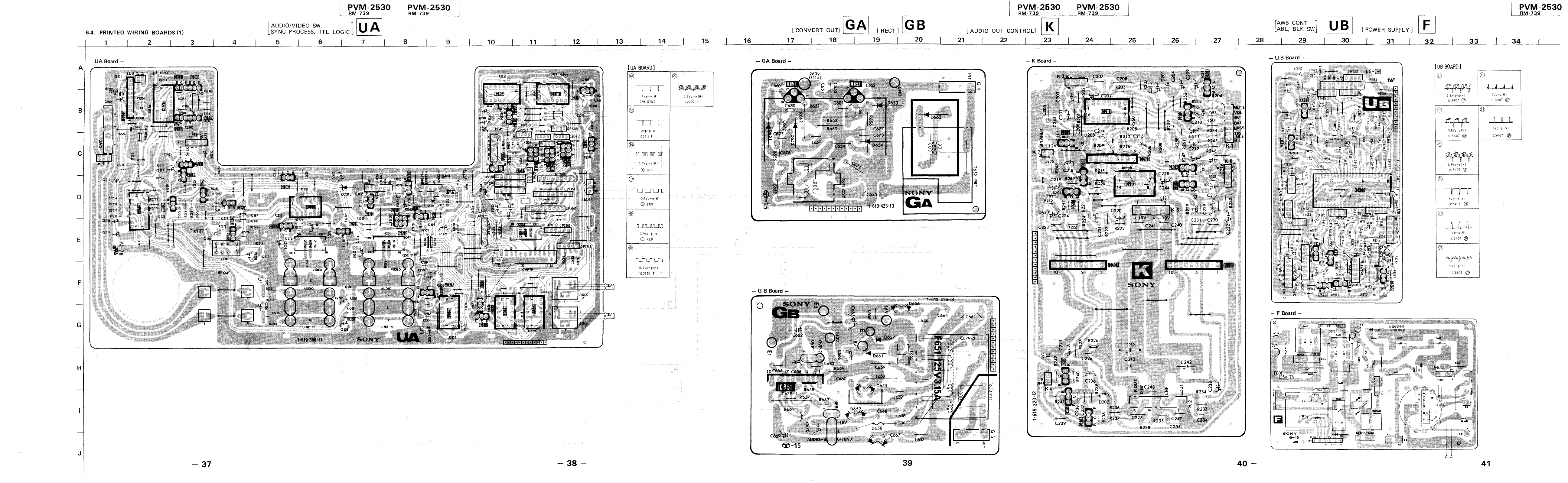
6-4. PRINTED WIRING BOARDS (11
1
2 3
4
f AUDIO/VIDEO SW.
LsvNc PRocEss. nL
5 6
0
/
"M-2530
~9
LOGIC] I U-AI
7
PVM.-2530
RM-739
8 9
10
11
12
13
14
15
16
I CONVERT OUT]
17 18
[ RECT]
19
20
I P\IM-2530
~39 _
[ AUDIO OUT CONTROL]
21 22 23
PVM-2530
RM-739
24
25
26 27
28
rAWB CONT ]
LABL, BLK SW
29
IUBI
[ POWER SUPPLY I
30
31
32
33
PVM-2530
RM- 739
34
-UABoard -
A
B
C
D
E
[UA BOARD]
@) @
-r-,ll°
! \l~-p I HI 0.8Vp-o(H1
cm SY~C Q2207 E
®
-or-L-:-
2Vp -pH I
02211 t·
@
lliTJCilI
G-.il'p-, 1~1
(1:, Bel
®
we_'-''-
0.7vo-rlHI
@ GR~
!@
"-~ _ flJL .... ::u l: i.
0.7\•p-p'H•
(_6) RED
@
UL --C'L
o r,,,p --P :e ,
Q 2'130 li
§~:§h.,~,;§
- GA Board-
- K Board -
- U B Board -
i
3.8Vp -nH 1
1::0-101@
--'
1w1-~, Vt
IC,4C7 ~-ijl
CD
1
3.8Vo-p:~
1naJ7 ~-'t·
Cl' p
~
:~'
CC4c;; @
__}L-J'LJL
4V>-p!Hl
'
n:-·
;JC'
,.;;a;,
4;'.·-;
j4•){ @
'-----
0\/~-,iH'
1t34J7 @
F
H
J
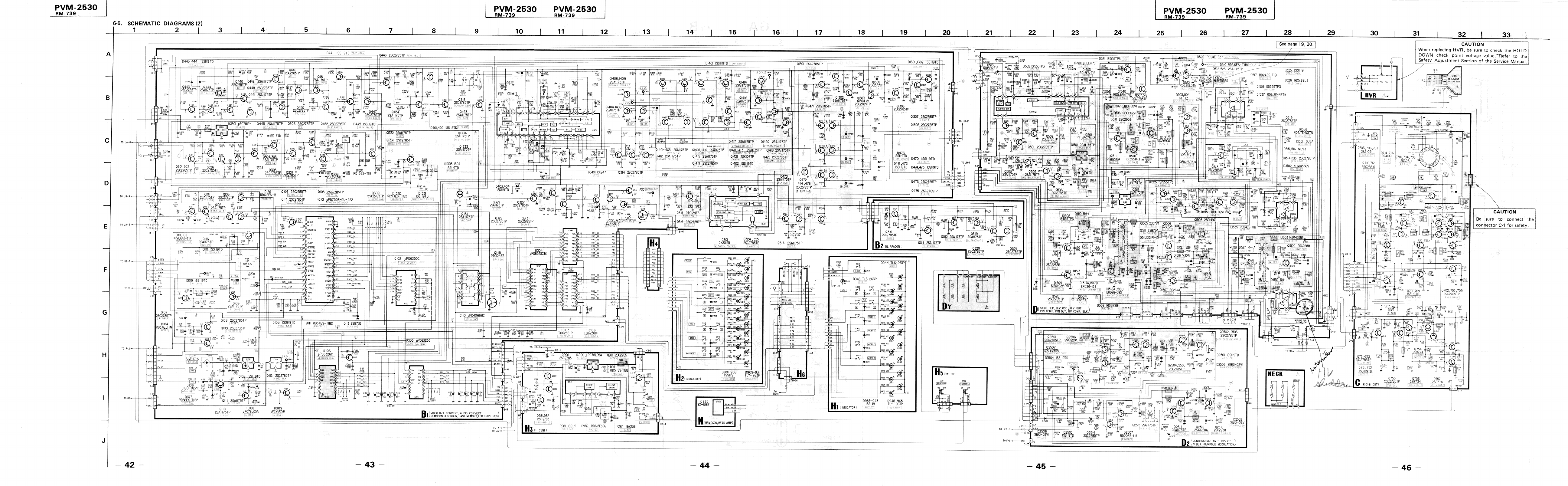
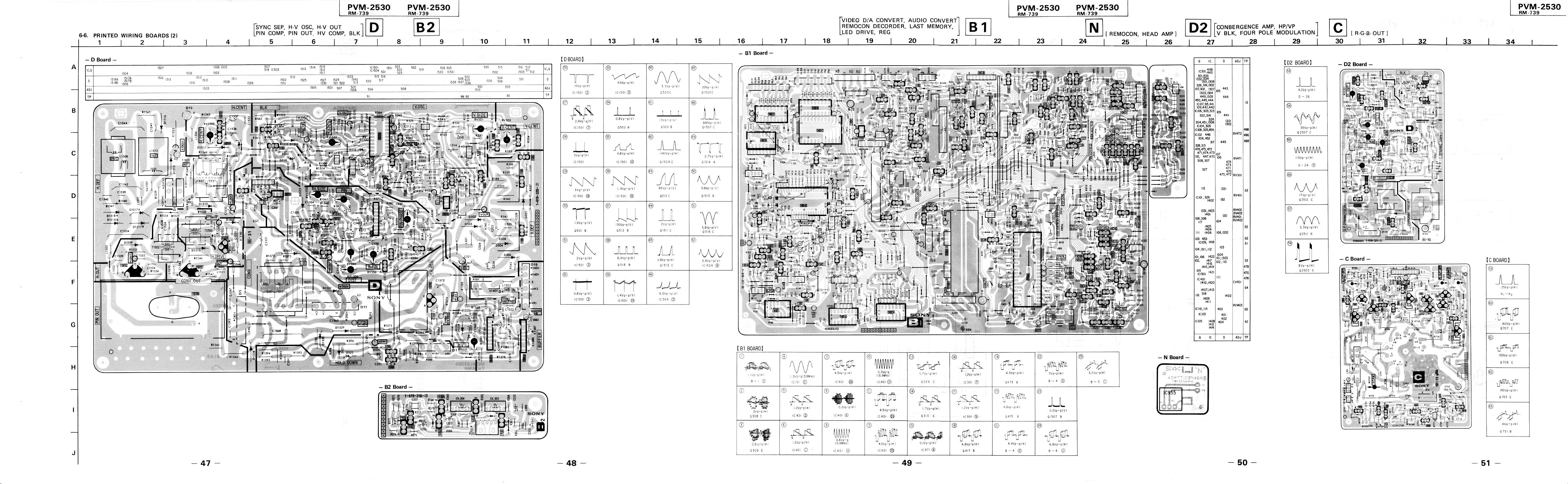
37 -
- 38 -
=
-GBBoard-
0
- 39 -
-- 40 -
- F Board -
1 ii .:~'~;,i £ '.:1~'~·-, .,,it"·
l,:1 1,,"+
~
- :'< < Ht- t/2; Y ;}:.·s~~
11
ii ~,,~11:1;7,,
Cil ~---=,·· r ,, : .• · [~1
w
so~~~
.,,~ ~-'. [!f·-1:J
.,,. f·I • ,
- 41
PVM-2530 I
PVM-2530
RM-739
PVM-2530
_______ AM-_7 39
PVM-2530 PVM-
RM- 739 ____ J!_M_-_
'---u.=-~~--
7ec3"'9
253
~----
0
RM)SISINDICATOR] L@ [8l] IHCENTJ
1 2 3
A
B
C
D
~~I
HS]~
7
8
9
10
11 12
"~~5 >
Cl'il,,i' ~,. ...
41 t;J
13
14
15
16 17
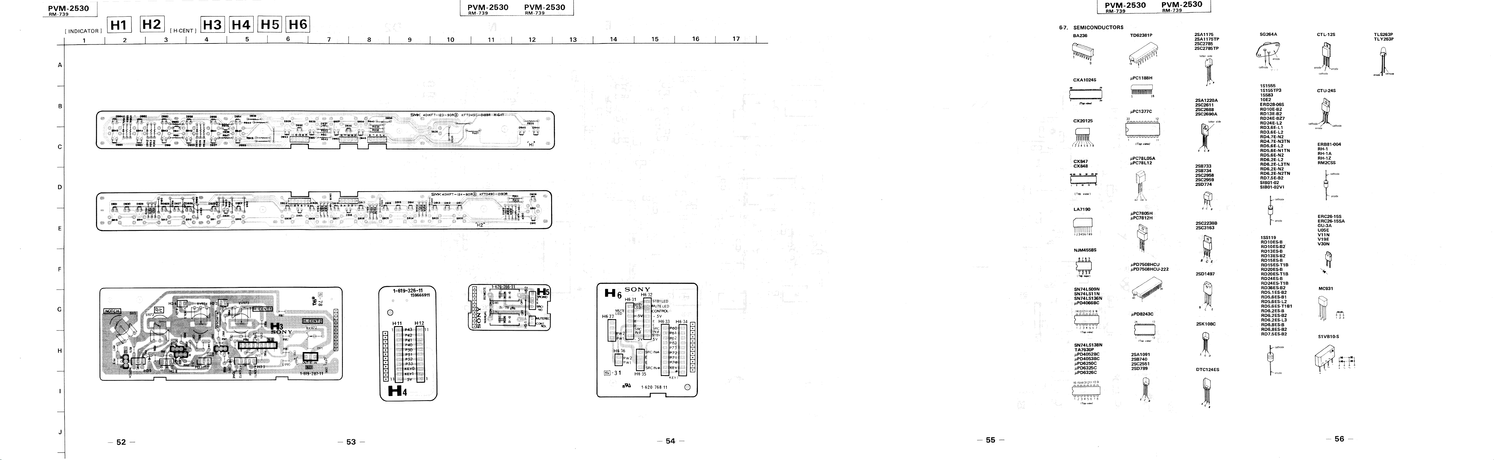
6-7. SEMICONDUCTORS
BA236
CXA1024S
•
•
CX20125
CXB47
CX848
r--~
' ' "
~
I
µPC118BH
1n~111111111m
µPC1377C
t::J
"
µPC78L05A
µPC78L12
2SA1175
2SA1175TP
2SC2785
2SC2785TP
etw ,.~•
i
i C •
2SA1220A
2SC2611
2SC2688
2SC2690A
28B733
2SB734
2SC2958
2SC2959
2$0774
SG264A
1S1555
1S155TP3
1SS83
10E2
ERD28-06S
RD10E·B2
RD13E-B2
RD24E-BZ7
RD24E-L2
RD3.6E-L 1
RD3.6E-L2
R04.7E-N2
RD4.7E-N3TN
R05,6E-L2
RD5.6E-N1TN
RD5.6E·N2
RD6.2E-L2
RD6.2E-L3TN
RD6.2E-N2
RD6.2E-N2TN
RD7.5E-B2
SIB01-02
Sl801-02VI
CTL-12S
CTU-24S
ERB81-004
RH-1
RH-1A
RH-12
RMZCSS
TLS263P
TLY263P
E
F
G
H
1-619-326-11
159666911
0
H·11 H·12
l ,;,_i, ·-f143· ,: 11
1 ,;p4z-
,-_•., "
1
-~·::
:t~~:l:;,t;:·.~~
'•k,d-.L.,_ •. c_ ,Clif<f•'t"7'<f·1i-, YL
•
'Pin
:p40
'PSO"",
')f-° KEl{f-:.
11 ·;f -,5v ,- t~. I
16 · ·1
~
Hs
VTElEO
ONTRQI.
®1:M 1-620 768-11
Htd4
e6o
pt, l
P62
P&A
p7f - , .
n
P:71
P-74:l
K'EY-.-,.
.,. ,,. .
1
KE'>'
0
LA7190
NJM4558S
a
, l J 4
( flll' TI<• I
SN74LS09N
SN74LS11N
SN74LS136N
µP04066BC
SN74LS138N
TA7630P
µPD4052BC
µPD4D53BC
µPD6250C
µPD6325C
,uPD6326C
10:a,~1}12" 10\l
c:::J
\ i l 4 ~, I. ' R
/To,,,,.,.!
µPC7805H
µPC7812H
i
',,
µPO7508HCU
µP07508HCU-222
µ.PD8243C
d
"
2SA1091
258740
2SC2551
2SD789
2SC2238B
2SC3163
~
'''
8 CE
2S01497
~
. -
C c
2SK108C
t
S C r,
DTC124ES
,i
•
1S$119
R010ES-B
RD10ES-Bi
RD13ES-B
RD13ES-B2
RD15ES-B
RD15ES-T1B
RD20ES-B
RD20ES-T1B
RD24ES-B
RD24ES-T1B
RD36ES-B2
RD5.1ES-82
R05.6ES-B1
R05.6ES-L2
RD5.6ES-T181
RD6.2ES-B
RD6.2ES-B2
RD6.2ES-L3
RD6.8ES-B
RD6.8ES-B2
RD7.5ES-B2
ERC26-15S
ERC26-15SA
GU-3A
U05E
V11N
V19E
V30N
MC931
S1VB10..S
J
- 52 -
- 53 -
54 -
-- 55 -
-- 56
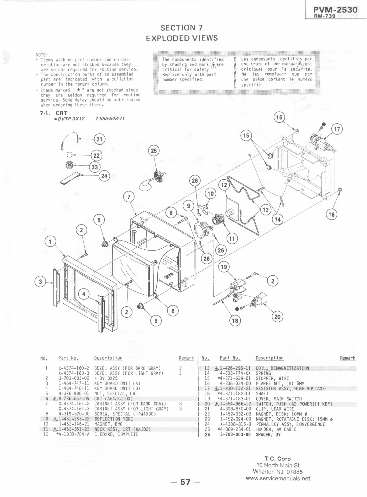
SECTION 7
EXPLODED VIEWS
PVM-2530
RM-739
NOTE:
Items with no part number and no description are not stocked because they
are seldom required for routine service.
The construction parts of an assembled
part are indicated with a collation
number in the remark column.
Items marked
they are seldom required for routine
service. Some delay should be anticipated
when ordering these items.
7-1. CRT
11 * 11
•BVTP 3X12
are not stocked since
7-685-648-71
Les composants
une trame et une
critiques pour la
Ne les remplacer que par
une piece portant le numero
spec i fie.
Part No.
No.
X-4374-160-2
X-4374-160-3
2
3-703-083-00
3 l-464-747-11
4
l-464-748-11
5
4-376-980-01
6
fr,.8-736-65 2-05
7
X-4374-161-2
X-4374-161-3
8
4-319-520-00
9
fr..l-451-255-22
10
1-452-146-21
11
&. l-452-351-22
12
*A-1330-784-A
Description
BEZEi_ ASSY ( FOR DARK GRAY)
BEZEi_ ASSY ( FOR I_IGHT GRAY)
+ BV 3X25
KEY BOARD UNIT (A)
KEY BOARD UNIT (B)
NUT, SPECIAi_, CRT
CRT (A64JKJ10X)
CABINET ASSY (FOR DARK GRAY)
CABINET ASSY (FOR LIGHT GRAY)
SCREW, S PECIAI_ ( +PW4X30)
OEFI_ECTI ON YOKE
MAGNET, BMC
NECK ASSY, CRT (NA302)
C BOARD, COMPI_ETE
6
Remark I No.
--i-
2
2
8
8
- 57
20
Part No.
13
&, 1-426-296-11 COIL, DEMAGNETIZATION
I
14
I
I
I
I
I
I
I
I
I
I
I
I
I
4-303-774-XX SPRING
15
*4-371-629-01 STOPPER, WIRE
16
4-306-034-00
17
&..1-230-712-21
18
*4-371-182-01 SHAFT
19
*4-371-183-01 COVER, MAIN SW ITCH
20
it, 1-554-966-12 SWITCH, PUSH (AC PGJER)( 1 KEY)
21
4-308-870-00
22
1-452-032-00 MAGNET, DISK; lOMM
23
1-452-094-00 MAGNET, ROTATABLE DISK; 15MM
24
X-4308-815-0
25
*4-369-234-01
3-703-003-00
26
-
Description
FLANGE NUT, (B) 5MM
RESISTOR ASSY, HIGH-VOi_ TAGE·
CUP, I_EAD WIRE
PERMALLOY ASSY, CONVERGENCE
HQI_DER. HV CAB1_E
~
SPACER, DY
T.C . Corp
10 North Main St
Wharton NJ 07885
www.servicemanuals.net
Remark
~
PVM-2530
RM-739
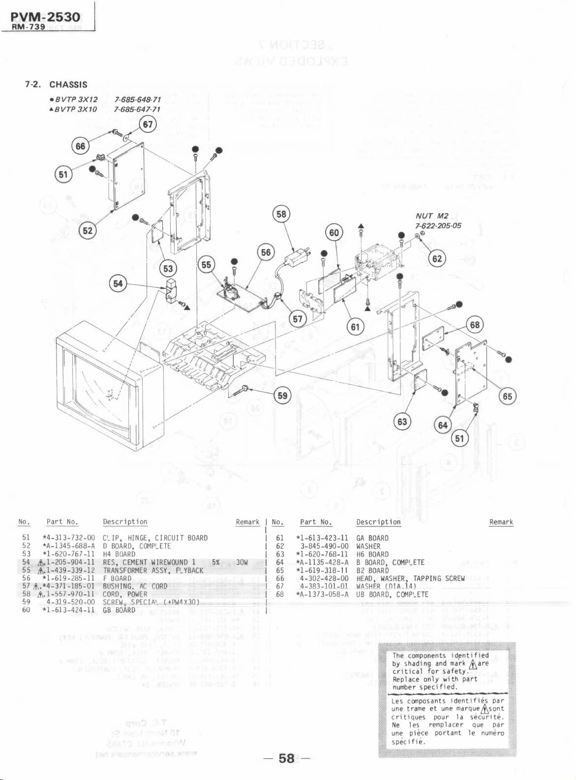
7-2. CHASSIS
•BVTP 3X12
7-685-648- 71
No. Part No. Description
51
*4-313-732-00
52
*A-1345-688-A
53
*l-620-767 -11
54
&.1-205-904-11 RES, CEMENT WIREWOUND 1 5%
55
&.1-439-339-12 TRANSFORMER ASSY, FI_YBACK
56
*l-619-285-11
57 it,...*4-371-185-01
58
h,.1-557-970-11
59
4-319-520-00 SCREW, SPECIAi_ (+PW4X30)
60
*l-613-424-11
c1_ IP,
HINGE, CIRCUIT BOARD
D BOARD, COMPI_ ETE
H4 BOARD
F BOARD
BUSH ING. AC CORD
CORD, POWER
GB BOARD
Remark
30W
I~
I
I
I
I
I
I
I
I
I
Part No. Description Remark
61
*l-613-423-11 GA BOARD
62 3-845-490-00
63 *l-620-768-11 H6 BOARD
64 *A-1135-428-A B BOARD, COMPLETE
65 *l-619-318-11
66 4-302-428-00
67
4-383-101-01
68 *A-1373-058-A UB BOARD, COMP1_ETE
WASHER
B2 BOARD
HEAD, WASHER, TAPPING SCREW
WASHFR (nTA ,14)
I
I
- 58 -
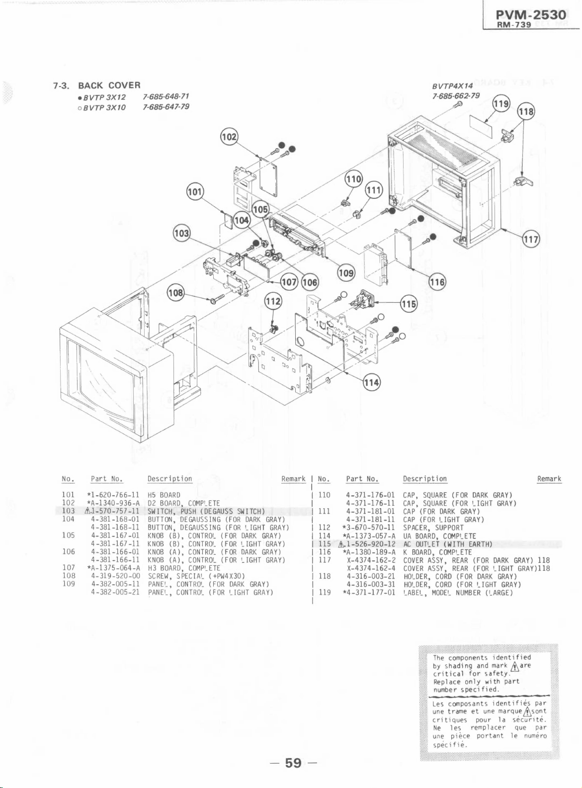
7-3. BACK COVER
•BVTP 3X12
oBVTP 3X10
7-685-648-71
7-685-647-79
PVM-2530
RM-739
Part No.
No.
101
*l-620-766-11
102
*A-1340-936-A
103
&.1-570-757 -11
104
4-381-168-01
4-381-168-11
105
4-381-167-01
4-381-167 -ll
106
4-381-166-01
4-381-166-11
107
*A-1375-064-A
108 4-319-520-00
109
4-382-005-11
4-382-005- 21
Description
H5 BOARD
D2 BOARD, COMPI_ ETE
SWITCH, PUSH (DEGAUSS SWITCH)
BUTTON, DEGAUSSING (FOR DARK GRAY)
BUTTON, DEGAUSSING (FOR UGHT GRAY)
KNOB (B), CONTROi_ (FOR DARK GRAY)
KNOB (B), CONTROL (FOR LIGHT GRAY)
KNOB (A), CONTROL (FOR DARK GRAY)
KNOB (A), CONTROL (FOR LIGHT GRAY)
H3 BOARD, COMPt_ETE
SCREW, SPECIAi_ (+PW4X30)
1
PANE
_ , CONTR01_ (FOR DARK GRAY)
PANEL, CONTROL (FOR LIGHT GRAY)
Remark I No.
--i-
- 59 -
110
I
I
111
I
I
112
I
114
I
115
I
116
I
117
I
I
118
I
I
119
I
I
Part No.
4-371-176-01
4-371-176-11
4-371-181-01
4-371-181-11
*3-670-570-11
*A-1373-057-A
&.1-526-920-12
*A-1380-189-A
X-4374-162-2
X-4374-162-4
4-316-003-21
4-316-003-31
*4-371-177-01
Description Remark
CAP, SQUARE
CAP, SQUARE (FOR UGHT GRAY)
CAP (FOR DARK GRAY)
CAP (FOR LIGHT GRAY)
SPACER, SUPPORT
UA BOARD, COMP!_ETE
AC OUTLET (WITH EARTH)
K BOARD, COMPI_ETE
COVER ASSY, REAR (FOR DARK GRAY) 118
COVER ASSY, REAR (FOR LIGHT GRAY)ll8
HOLDER, CORD (FOR DARK GRAY)
HOLDER, CORD (FOR LIGHT GRAY)
LABEi_, MODEL NUMBER (LARGE)
(FOR DARK GRAY)
Les composants identi
une trame et une
critiques pour la
Ne les remplacer que par
une piece portant le numero
speci fie.
PVM -2530
RM-739
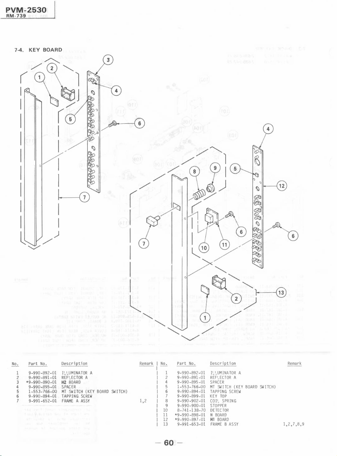
7-4. KEY BOARD
0
-@
Part No.
No.
1
9-990-892-01
2 9-990-891-01
3 *9-990-890-01
4
9-990-895-01
5
1-553-766-00
6
9-990-894-01
7
9-991-652-01
Description
1
I '-
_ UM I NA TOR A
REFt_ECTOR A
H2 BOARD
SPACER
MT SW ITCH ( KEY BOARD SW ITCH) 6
TAPPING SCREW
FRAME A ASSY
Remark
No.
1,2 8
10 8-741-138-70
11
12
13
- 60 -
Part No. Description Remark
1
9-990-892-01
2
9-990-891-01
4
9-990-895 -01
5
1-553-766-00
9-990-894-01 TAPPING SCREW
7
9-990-899-01
9-990-902-01
9 9-990-900-01 STOPPER
*9-990-898-01
*9-990-897-01
9-991-653-01
l'_ 1_UM INA TOR A
REFt_ECTOR A
SPACER
MT SWITCH (KEY BOARD SWITCH)
KEY TOP
1
CO 1
_ S PR I N G
DETECTOR
N BOARD
Hl BOARD
FRAME B ASSY
1,2,7 ,8,9
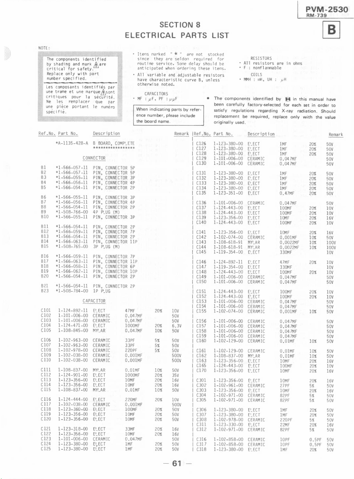
SECTION 8
ELECTRICAL PARTS LIST
PVM-2530
RM-739
Ref.No. Part No. Description
*A-1135-428-A
B BOARD, COMP1.ETE
*****************
CONNECTOR
Bl
*l-566-057-11
B2
*l-566-057-11
B3
*l-566-055-11
B4
*l-566-056-11
B5
*l-566-054-11 PIN, CONNECTOR 2P
B6
* 1-566-055-11
B7
*l-566-056-11
B8
*l-566-054-11
B9
*l-508-766-00
BlO
*l-566-055-11
Bll
*l-566-054-11
B12
*l-566-059-11
Bl3
*l-566-054-11
Bl4
* l-566-063-11
Bl5
*l-508-765-00
Bl6
*l-566-059-11
B17
*l-566-063-11
Bl8
*l-566-058-11
Bl9
* 1-566-062-11
B20
*l-566-054-11
B21
*l-566-054-11
B23
*l-508-784-00
PIN, CONNECTOR 5P
PIN, CONNECTOR 5P
PIN, CONNECTOR 3P
PIN, CONNECTOR 4P
PIN, CONNECTOR 3P
PIN, CONNECTOR 4P
PIN, CONNECTOR 2P
4P f>1_UG (M)
PIN, CONNECTOR 3P
PIN,
CONNECTOR 2P
PIN, CONNECTOR 7P
PIN, CONNECTOR 2P
PIN, CONNECTOR llP
3P P'_UG (M)
PIN, CONNECTOR 7P
PIN, CONNECTOR llP
PIN, CONNECTOR 6P
PIN, CONNECTOR lOP
PIN, CONNECTOR 2P
PIN, CONNECTOR 2P
lP P'_UG
CAPACITOR
C 101
1-124-892-11
Cl02
1-101-006-00
Cl03
1-101-006-00
C104
1-124-4 71-00
C105
1-108-845-00
Cl06
1-102-963-00
Cl07
1-102-963-00
Cl08
1-102-978-00
Cl09
1-102-038-00 CERAMIC
C 110
1-102-038-00
Clll
1-108-837-00
C 112
1-124-901-00
C 113
1-123-356-00
C 114
1-123-356-00
C115
1-108-837-00
Cll6
1-124-444-00
C 117
1-102-038-00
Cll8
1-123-360-00
C 119
1-123-356-00
C 120
1-123-356-00
C 121
1-123-318-00
Cl22
l-123-356-00
Cl23
1-101-006-00 CERAMIC 0.047MF
Cl24
1-123-380-00 Et,.ECT lMF
C 125
1-123-380-00
E1_ECT
CERAMIC 0 .04 7MF
CERAMIC 0. 04 7MF
EECT
MYI_AR
CERAMIC 33PF
CERAMIC
CERAMIC 220PF
CERAMIC O.OOlMF
MY1.AR O.OlMF
E1_ECT
EI_ECT
E1.ECT lOMF
MY'.AR O.OlMF 10%
E1.ECT 220MF
CERAMIC
EECT lOOMF
El_ECT
E'.ECT
E'_ECT
E'.ECT
E!_ECT
lter:is marked " * " are not stocked
since they are seldom required for
routine service. Sor:ie delay should be
anticipated when ordering these items.
All variable and adjustable resistors
have characteristic curve 8, unless
otherwise noted.
CAPACITORS
MF : )J F , PF : µ µ F
When indicating parts by reference number, please include
the board name.
Remark
!Ref.No. Part No.
i-I
I
I
I
I
47MF
20%
lOV
50V
lOOOMF
0.047MF
50V Cl56
20%
6.3V Cl57
10% 50V
5% 50V
33PF
O.OOlMF
5% 50V
5%
50V
500V
500V Cl63
10%
lOOOMF
lOMF
50V
20% 35V
20% 16V
20% 16V
50V
O.OOlMF
lOMF
lOMF
33MF
lOMF
20% lOV
500V
20%
50V
20% 50V
20%
50V
20% 16V
20% 16V
50V
20% 50V
IMF
20%
50V
RESISTORS
All resistors are in ohms
F : nonfl ammab 1 e
COILS
MMH : 1nH, UH : fJH
• The components identified by B in this manual have
been carefully factory-selected for each set in order to
satisfy regulations regarding X-ray radiation. Should
replacement be required, replace only with the value
originally used.
Des er i pt ion
Cl26 1-12'3-380-00
Cl27
1-123-380-00
Cl28
1-123-380-00
Cl29
1-101-006-00
Cl30
1-101-006-00
Cl31
1-123-380-00
Cl32
1-123-380-00
Cl33
1-123-380-00
Cl34
1-123-380-00
Cl35
1-123-351-00
Cl36
1-101-006-00
Cl37
1-124-443-00
Cl38
1-124-443-00
Cl39
1-123-356-00
Cl40
1-124-443-00
Cl41
1-123-356-00
Cl42
1-102-074-00
Cl43
1-108-618-91
Cl44
1-108-618-91
Cl45
1-119-354-00
Cl46
1-124-892-11
Cl47
1-119-354-00
Cl48
1-124-443-00
Cl49
1-101-006-00
Cl50
1-101-006-00
Cl 51
1-124-443-00
Cl52
1-124-443-00
Cl53
1-101-006-00
Cl54
1-101-006-00
C155
1-102-074-00
1-101-006-00
1-101-006-00
Cl58
1-101-006-00
Cl59
1-101-006-00
Cl60
1-102-129-00
Cl61
1-102-129-00
Cl62
1-108-837-00
1-123-356-00
Cl65
1-124-443-00
Cl 70
1-123-356-00
C301
1-123-356-00
C302
1-102-961-00
C303
1-123-356-00
C304
1-102-971-00
C305
1-102-971-00
C306
1-123-380-00
C307
1-123-380-00
C308
1-102-978-00
C311
1-123-330-00
C312
1-102-971-00
C316
1-102-858-00 CERAMIC
C317
1-102-858-00
C318
1-123-380-00
E1.ECT
E1.ECT
E1.ECT
CERAMIC
CERAMIC
1
E
. ECT
E'_ ECT
E1_ECT
E1.ECT lMF
E1.ECT
CERAMIC
El_ECT
E1_ECT
E1_ECT
E1.ECT
E1_ECT
CERAMIC
MYI_AR
MY1_AR
E1_ECT
E1_ECT
El_ECT
E1_ECT
CERAMIC
CERAMIC
E1_ECT
lMF
lMF
lMF
0.047MF
0.047MF
lMF
lMF
lMF
0.47MF
0.047MF
lOOMF
lOOMF
lOMF
lOOMF
lOMF
0.00lMF
0.0022MF
0.0022MF
330MF
47MF
330MF
lOOMF
0.047MF
0.047MF
lOOMF
E'.ECT lOOMF
CERAMIC
CERAMIC
CERAMIC
CERAMIC
CERAMIC
CERAMIC
CERAMIC 0.047MF
CERAMIC
0.047MF
0.047MF
O.OOlMF
0.047MF
0.047MF
0.04 7MF
O.OlMF
CERAMIC O.OlMF
MY'.AR O.OlMF
1
E
_ ECT
E1_ECT
E1_ECT
E1_ECT
CERAMIC 27PF
E1_ECT
CERAMIC 82PF
CERAMIC 82PF
E'. ECT lMF
1
E
_ EC T
CERAMIC 220PF
1
E
_ ECT
CERAMIC
lOMF
lOOMF
lOMF
lOMF
lOMF
lMF
22MF
82PF
lOPF
CERAMIC lOPF
E'_ECT
lMF
20% 50V
20% 50V
20%
20%
20%
20%
20%
20% 50V
20%
20% lOV
20% 16V
20% lOV
20% 16V
10% 50V
10%
10% lOOV
20% lOV
20% lOV
20% lOV
20% lOV
10%
10% 50V
10% 50V
10% 50V
20%
20% lOV
20% 16V
20%
5% 50V
20%
5%
5% 50V
20% 50V
20% 50V
5% 50V
20% 16V
5% 50V
0.5PF
0.5PF
20% 50V
Remark
50V
50V
50V
50V
50V
50V
50V
50V
lOV
lOOV
lOV
lOV
50V
50V
50V
50V
50V
50V
50V
50V
50V
16V
16V
16V
50V
50V
50V
61
PVM-2530
RM -73 9
Ref. No. Part No. Description
C320 1-123-356-00
C 321
C324
C325 1-102-973-00
C326
C 327
C 329 1-102-971-00
C330 1-102-973-00
C 331 1-123-356-00
C332 1-101-006-00
C333 1-123-356-00 E'_ECT
C335 1-102-887-00
C401
C402 1-124-555-00
C403
C404
C405
C406
C407
C409
C410
C411 1-123-351-00
C412
C413
C414
C416
C418
C419
C420 1-124-896-00
C421
C440
C441
C442
C443 1-123-381-00 E'_ECT
C444
C445 1-124-478-11
C446 1-123-351-00 E!_ECT
C447
C 1301 1-123-330-00 E1_ECT
Cl302 1-124-896-00 E1_ECT
Cl303
Cl304
Cl305 1-106-196-00 MYI_AR
C 1306 1-102-971-00
C 1307
C 1308
C 1309 1-102-129-00
C 1310
Cl3ll 1-123-356-00
Cl333
C 1336
Cl338 1-124-478-11
Cl339 1-123-321-00,
1-102-888-00
1-101-006-00
1-12 3-380 -00
1-102-820-00
1-123-330-00
1-102-125-00
1-123-447-00 E'_ECT
l-102-129-00
1-123-447-00 E!_ECT
1-123-356-00 E1_ECT
1-102-865-00
1-102-074-00
1-123-351-00 E'_ECT
1-123-330-00
1-124-645-11
1-123-381-00 E!_ECT
1-123-318-00
1-123-607-00 E!_ECT
1-123-332-00
1-123-356-00
1-124-655-11
1-123-332-00
1-102-129-00
1-102-973-00
1-123-380-00
1-101-006-00
1-124-645-11
1-101-006-00
1-123-332-00
1-108-617-91 MY1_AR
1-108-618-91 MY1_AR
E1_ECT
CERAMIC 150PF
CERAMIC 0.047MF
CERAMIC lOOPF
EI_ECT
CERAMIC
CERAMIC 82PF
CERAMIC lOOPF
E1_ECT
CERAMIC 0.04 7MF
CERAMIC 47PF
EI_ECT
EI_ECT
CERAMIC
CERAMIC O.OlMF 10%
CERAMIC SPF 0.5PF
CERAMIC 0.00lMF 10%
EI_ECT
E!_ECT
E!_ECT
E!_ECT
E!_ECT
E!_ECT
EI_ECT
E!_ECT
E!_ECT
CERAMIC O.OlMF 10%
EI_ECT
CERAMIC
E!_ECT
CERAMIC 0.047MF
CERAMIC 82PF 5%
EI_ECT
CERAMIC
CERAMIC
E!_ECT
EI_ECT
El_ ECT
Et_ECT
lOMF
IMF
330PF
lOMF
lOMF
22MF 20%
lOOOMF
0 .004 7MF 10%
0. 22MF
0.22MF 20%
lOMF
0.47MF 20%
0.47MF
22MF
lOMF
2.2MF
33MF 20%
O.lMF
33MF 20%
47MF 20%
lOMF 20%
0.47MF 20%
47MF 20%
2.2MF 20%
lOOMF 20%
0.47MF 20%
lOOPF
22MF
33MF 20%
lMF
O.OlMF 10%
lOMF 20%
0.047MF
O.OlMF 10%
47MF
lOMF
0 .0018MF 10%
0.0022MF 10%
lOOMF
220MF
20%
5%
5%
20%
5%
5%
5%
20%
20%
5%
20%
20%
20%
20%
20%
20%
20%
20%
5%
20%
20%
20%
20%
20%
20% ·
Remark !Ref.No. Part No.
16V
50V
50V
50V
50V
50V
50V
50V
16V
50V
16V
50V
16V
16V
50V
50V
50V
50V
16V
50V
50V
50V
50V
16V
16V
50V
16V
50V
16V
16V
16V
50V
16V
50V
50V
25V
50V
50V
16V
16V
50V
50V
lOOV
50V
16V
50V
50V
16V
16V
lOOV
lOOV
25V
16V
Cl340 1-123-380-00 E1_ECT
Cl341 1-123-380-00 E1_ECT
Cl342
1-108-630-91 MY1_AR
C1343
1-136-165-00
Cl344
1-102-973-00
Cl401
1-102-074-00
Cl402
1-123-332-00
Cl403
1-102-129-00
Cl404
1-123-318-00 E1_ECT
CV401
1-141-147-XX
DlOl
8-719-109-95
Dl02
8-719-109-95
Dl03
8-719-911-19
Dl04
8-719-101-39
0105
8-719-511-20
0106
8-719-920-02
0107
8-719-110-83
0108 fr.,.8-719-921-20
0109
8-719-911-19
0110
8-719-911-19
0111 8-719-109-85
Dl18
8-719-109-91
0120
8-719-110-34
Dl26 8-719-109-91
0129
8-719-109-91
0131
8-719-109-91
0132
8-719-109-91
D401
8-719-911-19
D402
8-719-911-19
D403 8-719-911-19
D404 8-719-911-19
D441 8-719-911-19
0443
8-719-911-19
0444
8-719-911-19
0445 8-719-911-19
0470
8-719-911-19
0471 8-719-911-19
0472
8-719-911-19
0473 8-719-911-19
0474
8-719-~l l-l 9
0475 8-719-911-19
01301 8-719-911-19
01302 8-719-911-19
01303 8-719-911-19
01304 8-719-911-19
01331 8-719-911-19
01332
8-719-109-85
01401 8-719-911-19
01402
8-719-911-19
Description
F II_M
CERAMIC lOOPF
CERAMIC 0.00lMF
E'_ECT
CERAMIC
TRIMMER
CAP, TRIMMER
DIODE
DI ODE
RD6.8ES-B
DIODE RD6.8ES-B
DIODE 1S5119
DI ODE RD3.6E-1_2
S1VB20
DIODE
DI ODE ERB12-02
DI ODE RD36ES-B2
DIODE lSS..t 19TD
DI ODE 1S5119
DI ODE 1S5119
DIODE
RD5.1ES-B2
DI ODE
RD6.2ES-B
DIODE RD13ES-B
DIODE
RD6.2ES-B
DIODE RD6.2ES-B
DI ODE RD6.2ES-B
DIODE RD6.2ES-B
DI ODE 1SS119
15S119
DI ODE
DIODE 1SS119
DIODE 1SS119
1SS119
DI ODE
1SS119
DIODE
DI ODE 15S119
DI ODE 1SS119
DIODE 1SS119
DIODE 1SS119
DI ODE 15S119
1SS119
DI ODE
DIODE 1SS119
DIODE 1S5119
DIODE 1SS119
DI ODE 15S119
DIODE 1SS119
DIODE 1SS119
1SS119
DIODE
DIODE
RD5.1ES-B2
1SS119
DIODE
DIODE 15S119
lMF
lMF
0. 022MF
O.lMF
47MF
O.OlMF
33MF
Remark
20%
50V
20%
50V
10%
lOOV
5%
50V
5%
50V
10%
50V
20%
16V
10%
50V
20% 16V
- 62 -
The components identified
by .s~ading and mark &are
cr1t1cal for safety.
Repl ace only with part
number specifie d.
PVM-2530
RM-739
00
Ref. No. Part
D'-301
1
0
_ 302
IClOl
IC102
IC103 &.8-759-102-28
IC104
IC105
IC106
IC107
IC 108 &8-759-108-05
IC109
ICllO
IC301
IC401
IC1301&8-759-171-12
J201
'-101
1_102
1_103
I_ 104
1_105
!_106
1_301
1_ 302
1_303
1_ 304
1
_ 305
1
_306
I_ 307
1_ 308
1_401
1_402
1_404
I_ 1330
,_ 13 31
0101
Ql02
Ql03
Ql04
Ql05
No. Description
1-415- 280-00
1-415-510-11
8-759-105-89
8-759-102-12
8-759-182-43
8-759-104-05
8-759-207-07
8-759-207-07
8-759-171-05
8~759-140-66
8-759-913-11
8-758-480-00
*l-564-529-11
1-407-708-00
1-407-708-00
1-408-424-00
1-408-424-00
1-408-424-00
1-408-4 24-00
1-408-412-00
1-407-571-00
1.:408-412-00
1-408-411-00
1-408-411-00
1-408-417-00
1-408-412-00
1-409-193-00
1-408-398-00
1-408-398-00
1-408-398-00
1-408-236-00
1-407 -364-00
8-729-117-54
8-729-117-54
8-729-178-54
8-729-178-54
8-729-178-54
0106 8-729-117-54
0107
8-729-178-54
Ql08
8-729-178-54
DE1_A Y 1_ I NE
1
DEI_AY
_ INE (1 H)
1
DE1_AY
_ INE, Y
IC
IC UPD7508HCU-222
UPD6250C
IC
UPD6326C
IC
UPD8243C(M)
IC
UPD6325C
IC
TD62381 P
IC
TD62381P
IC
UPC781_05A
IC
UPC 7805H
IC
UPD4066BC
IC
CX20125
IC
IC CX848
IC MPC7812H
CONNECTOR
CONNECTOR,
BOARD TO BOARD 5P
COI'_
MICRO
INOUCTOR 18UUH
MICRO INDUCTOR 180UH
MICRO INDUCTOR l80UH
MICRO INDUCTOR 180UH
MICRO INDUCTOR 180UH
MICRO INDUCTOR 180UH
MICRO INDUCTOR 18UH
COIL, VARIAB~E 22UH
MICRO INDUCTOR 18UH
MICRO INDUCTOR 15UH
MICRO
INDUCTOR l 5UH
MICRO INDUCTOR 47UH
MICRO INDUCTOR 18UH
COIi_ 3.58MHz TRAP
MICRO INDUCTOR l.2UH
MICRO INDUCTOR 1.2UH
MICRO INDUCTOR l.2UH
MICRO INDUCTOR 2.7MMH
1
CO 1
_, SPOOK CHOKE 3. 3UH
TRANS IS TOR
TRANSISTOR 2SA1175
TRANSISTOR 2SA1175
TRANSISTOR 2SC2785
TRANSISTOR 2SC2785
TRANSISTOR 2SC2785
TRANSISTOR 2SA1175
TRANSISTOR 2SC2785
TRANSISTOR 2SC2785
Remark
I Ref.No. Part No.
Description
Ql09
8-729-178-54
QllO ,t.8-729-101-54
Qlll
8-729-117-54
Qll2
8-729-178-54
Q113 8-729-373-92
Q115
8-729-900-36
Qll6
8-729-117-54
0117
8-729-178-54
0301
8-729-178-54
Q302
8-729-178-54
0303
8-729-178-54
0304
8-729-117-54
Q305
8-729-117-54
Q306
8-729-178-54
0307
8-729-178-54
Q308
8-729-178-54
Q309
8-729-178-54
Q313
8-729-178-54
Q314
8-729-178-54
Q315
8-729-900-36
Q316
8-729-178-54
Q317
8-729-117-54
Q318
8-729-178-54
0322 8-729-600-12
Q323
8-729-600-12
Q324
8-729-178-54
0325 8-729-178-54
Q326
8-729-178-54
Q327
8-729-178-54
0328 8-729-178-54
Q329
8-729-117-54
0440 &.8-729-101-36 TRANSISTOR 2SC2785TP-H
Q441
8-729-117-54
Q442
8-729-178-54
Q443
8-729-178-54
Q444
8-729-117-54
Q445
8-729-117-54
0446
8-729-178-54
0447
8-729-178-54
0448
8-729-178-54
0449
8-729-117-54
0450
8-729-178-54
Q451
8-729-117 -54
Q452
8-729-178-54
Q453
8-729-P 7-54 TRANSISTOR 2SA1175
Q454
8-729-117-54
0470
8-729-117-54
Q471
8-729-178-54
0472
8-729-178-54
0473
8-729-178-54
0474
8-729-178-54
Q475
8-729-178-54
Q476
8-729-178-54
TRANSISTOR 2SC2785
TRANSISTOR 2SA1175TP-F
TRANSISTOR 2SA1175
TRANSISTOR 2SC2785
TRANSISTOR 2SB739
TRANSISTOR DTC124ES
TRANSISTOR 2SA1175
TRANSISTOR 2SC2785
TRANSISTOR 2SC2785
TRANSISTOR 2SC2785
TRANSISTOR 2SC2785
TRANSISTOR 2SA1175
TRANSISTOR 2SA1175
TRANSISTOR 2SC2785
TRANSISTOR 2SC2785
TRANSISTOR 2SC2785
TRANSISTOR 2SC2785
TRANSISTOR 2SC2785
TRANSISTOR 2SC2785
TRANSISTOR DTC124ES
TRANSISTOR 2SC2785
TRANSISTOR 2SA1175
TRANSISTOR 2SC2785
TRANSISTOR 2SK108
TRANSISTOR 2SK108
TRANSISTOR 2SC2785
TRANSISTOR 2SC2785
TRANSISTOR 2SC2785
TRANSISTOR 2SC2785
TRANSISTOR 2SC2785
TRANSISTOR 2SA1175
TRANSISTOR 2SA1175
TRANSISTOR 2SC2785
TRANSISTOR 2SC2785
TRANSISTOR 2SA1175
TRANSISTOR 2SA1175
TRANSISTOR 2SC2785
TRANSISTOR 2SC2785
TRANSISTOR 2SC2785
TRANSISTOR 2SA1175
TRANSISTOR 2SC2785
TRANSISTOR 2SA1175
TRANSISTOR 2SC2785
TRANSISTOR 2SA1175
TRANSISTOR 2SA1175
TRANSISTOR 2SC2785
TRANSISTOR 2SC2785
TRANSISTOR 2SC2785
TRANSISTOR 2SC2785
TRANSISTOR 2SC2785
TRANSISTOR 2SC2785
Remark
- 63 -
Les composants identifies par
une trame et une marque&sont
critiques pour la securite.
Ne l es remp l acer q ue par
une piece portant le numero
specifie.
PVM -2530
RM-739
00
Ref.No. Part No.
Ql301
8-729-178-54
Ql302
8-729-117-54 TRANSISTOR 2SA1175
Ql303
8-729-178-54
Ql304
8-729-178-54
Ql305
8-729-178-54
Ql306
8-729-178-54
Ql307
8-729-178-54
Ql308
8-729-178-54
Ql311
8-729-117-54 TRANSISTOR 2SA1175
01331
8-729-178-54 TRANSISTOR 2SC2785
01332
8- 729-117 -54
01333 8-729-117-54
01334
8-729-117-54 TRANSISTOR 2SA1175
01401
8-729-117-54 TRANSISTOR 2SA1175
01402
8-729-117-54 TRANSISTOR 2SA1175
01403 8-729-117-54
01404
8-729-117-54 TRANSISTOR 2SA1175
01405
8-729-117-54 TRANSISTOR 2SA1175
01406
8-729-117-54 TRANSISTOR 2SA1175
01407
8-729-117-54
01408
8-729-117 -54
01409
8-729-117-54 TRANSISTOR 2SA1175
01410
8-729-117 -54 TRANSISTOR 2SA1175
01411
8-729-117-54
01412
8-729-117-54 TRANSISTOR 2SA1175
Ql413
8-729-117-54 TRANSISTOR 2SA1175
01414
8-729-117-54
01415
8-729-117-54 TRANSISTOR 2SA1175
01416
8-729-117-54 TRANSISTOR 2SA1175
Ql417
8-729-117-54 TRANSISTOR 2SA1175
01418
8-729-117-54 TRANSISTOR 2SA1175
01419
8-729-178-54
01420
8-729-117-54
01421
8-729-600-12 TRANSISTOR 2SK108
01422
8-729-178-54 TRANSISTOR 2SC2785
RlOl
1-247-787-00 CARBON 15
Rl02
1-247-787-00
Rl03
1-249-441-11 CARBON
Rl04
1-249-441-11
Rl05
1-247-805-00
Rl06
1-247-823-00
1-249- 421-11
Rl07
Rl08
1-249-43 3-11 CARBON 22K
Rl09
1-249-433-11 CARBON
R110
1-249-465-11 CARBON
R111
1-249-437-11 CARBON
Rl12'
1-24 7-851-00
Rl13
1-249-421-11 CARBON 2 .2K 5% l/6W F Rl68
R114
1-249-421-11 CARBON
R115
1-249-425-11
Rl16
1-249-414-11
#
Description
TRANSISTOR 2SC2785
TRANSISTOR 2SC2785
TRANSISTOR 2SC2785
TRANSISTOR 2SC2785
TRANSISTOR 2SC2785
TRANSISTOR 2SC2785
TRANSISTOR 2SC2785
TRANSISTOR 2SA1175
TRANSISTOR 2SA1175
TRANSISTOR 2SA1175
TRANSISTOR 2SA1175
TRANSISTOR 2SA1175
TRANSISTOR 2SA1175
TRANS I srn·R 2SA 1175
TRANSISTOR 2SC2785
TRANSISTOR 2SA1175
RES IS TOR
CARBON 15
CARBON
CARBON
CARBON
CARBON 2.2K
CARBON
CARBON 4.7K 5% l/6W
•CARBON
5%
5%
lOOK
5% l/6W
lOOK
5% l/6W
82
5%
470
5%
5%
5%
22K
5% l/6W
47K
5%
47K
5%
6.8K
5%
2. 2K
5% l/6W F
560 5%
Remark
!Ref.No. Part No.
R117
R118
Rl19
Rl20
Rl21
Rl22
Rl23
Rl24
Rl25
Rl26
Rl28
Rl29 1-249-421-11
Rl30
Rl31
Rl32
Rl33
Rl34
Rl35 1-249-421-11
Rl36
Rl37 1-249-421-11
Rl38
Rl40 1-249-421-11
R141
Rl42 1-249-421-11
Rl43 1-249-421-11
Rl44
Rl45
Rl46 1-249-421-11
Rl47
R148
R149
Rl50
Rl51
Rl52
R153
Rl 54
l/6W
l/6W
l/6W
l/6W Rl61
l/6W
l/6W
1/4W Rl64
l/6W
l/6W
l/6W
R155
Rl56
Rl57
Rl58
Rl59
R160
Rl62
Rl63
Rl65
Rl66
Rl67
Rl 71 1-247-791-00
n1 7"J
I"\.&. IL
Rl73
Description
1-249-429-11
1-249-429-11
1-249-441-11
l-249-382-11
1-247-739-11
1-249-389-11
1-247-845-00
l -249-469-11
1-249-433-11
1-247-726-11
l-249-405-11 CARBON 100
1-247-706-11
1-249-417-11
1-249-417-11
1-249-421-11
1-249-421-11
1-249-421-11
1-249-421-11
1-249-421-11 CARBON 2.2K
l-247-710-11 CARBON 560
1-249-421-11
1-249-421-11 CARBON 2.2K 5% l/6W
l-249-414-11
1-247-883-00
1-249-422-11 CARBON
l-247-845-00 CARBON
1-249-421-11
1-249-421-11
1-249-421-11
1-249-421-11
1-247-717-11 CARBON 2. 2K 5% l/4W
1-247-791-00
1-247-791-00
1-247-791-00
l-247-791-00 CARBON 22 5%
1-247-791-00 CARBON
1-247-791-00 CARBON
1-247-791-00 CARBON
1-247-791-00 CARBON
1-247-791-00 CARBON
1-247-791-00 CARBON
l-247-791-00 CARBON
1-247-791-00
l-247 - 791-00 CARBON
1-247-791-00
CARBON lOK
CARBON
CARBON
CARBON
CARBON
CARBON
CARBON
CARBON 100K
CARBON 22K
CARBON
CARBON 2.2K 5%
CARBON 330 5%
CARBON lK
CARBON
CARBON
CARBON 2.2K
CARBON 2.2K 5% l/6W
CARBON 2.2K
CARBON 2.2K
CARBON 2.2K 5% l/6W
CARBON 2. 2K 5% l/6W
CARBON 2.2K
CARBON 2.2K
CARBON 2.2K
CARBON 2.2K
CARBON
CARBON
CARBON 2.2K 5% l/6W
CARBON 2. 2K 5%
CARBON 2. 2K 5% l/6W
CARBON 2. 2K 5% l/6W
CARBON 22 5% 1/6W
CARBON
CARBON
CARBON
CARBON
CARBON
5% 1/6W
lOK
5%
100K 5%
1.2
100
4.7 5%
3. 9K 5%
33K
lK
2.2K 5%
560
150K
2.7K
3.9K 5%
22 5% 1/6W
22 5% l/6W
22
22 5%
22 5% l/6W
22 5% 1/6W
22
22
22 5% l/6W
22 5%
22 5% l/6W
22 5% 1/6!.J
22 5%
1/6W
l/6W
5% l/6W F
5%
l/2W F
1/6W F
l/6W
5% l/4W
5%
l/6W
5% l/4W
5% l/6W
l/6W
l/4W
5% l/6W
5% 1/6W
l/6W
5% l/6W
1/6W
5%
1/6W
5%
5% l/6W
l/6W
5%
5% l/6W
5% l/4W
1/6W
5%
5% l/6W
5% l/6W
1/6W
5%
5% 1/6W
1/6W
1/6W
1/6W
l/6W
5%
l/6W
1/6W
5%
1/6W
5%
l/6W
l/6W
Remark
- 64 -
 Loading...