

Page 1
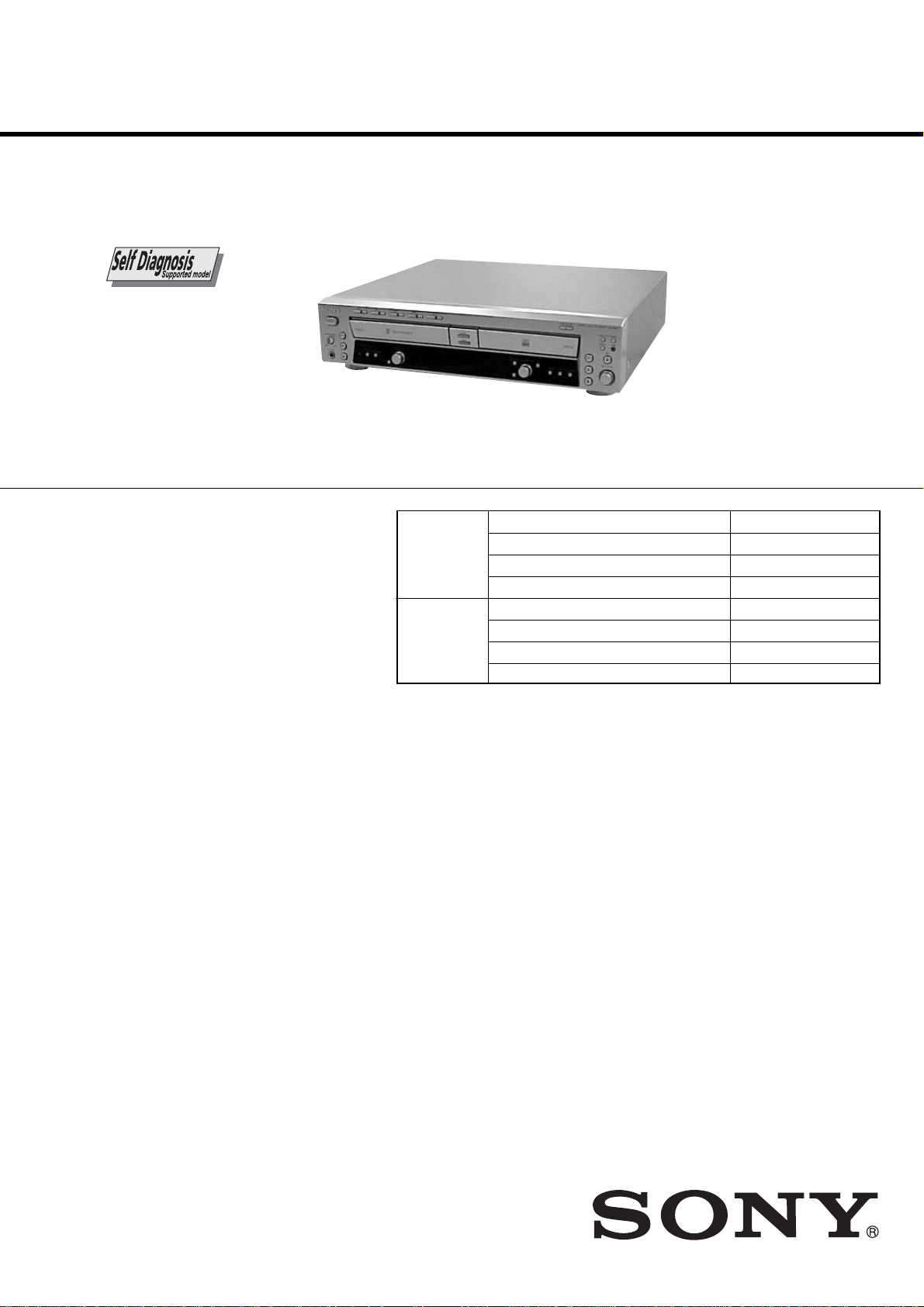
RCD-W50C
SERVICE MANUAL
Ver 1.1 2003. 12
Model Name Using Similar Mechanism NEW
CD Section
CD-R/CD-RW
Section
CD Mechanism Type CDM53L-30B61B
Base Unit Type BU-30BBD61B
Optical Pick-up Type A-MAX.3
Model Name Using Similar Mechanism NEW
CD Mechanism Type CDM65-RBD1
Base Unit Type RBD1
Optical Pick-up Type KRM-220CAA
US Model
Canadian Model
E Model
DECK A (the CD player section)
System Compact disc digital audio
Laser Semiconductor laser (λ =
Frequency response 20 Hz – 20,000 Hz (±0.5
DECK B (the CD-R and CD-RW
recording section)
System Compact disc digital audio
Laser Semiconductor laser (λ =
Playable discs CD, CD-R, CD-RW
Recordable discs CD-R, CD-RW (for music
Frequency response 20 Hz - 20,000 Hz (±0.5
system
780 nm)
Emission duration:
continuous
dB)
system
780 nm)
Emission duration:
continuous
use)
dB)
SPECIFICATIONS
Inputs
ANALOG IN
(Phono jacks) Impedance: 47 kilohms
DIGITAL OPTICAL IN
(Square optical connector jack)
Outputs
ANALOG OUT
(Phono jacks) Impedance: 47 kilohms
DIGITAL OPTICAL OUT
(Square optical connector jack)
PHONES
(Phono jack) Load impedance: 32 ohms
Rated input: 500 mVrms
Minimum input
250 mVrms
Optical wavelength:
660 nm
Rated output: 2 Vrms
Load impedance: over
10 kilohms
Wavelength: 660 nm
Output level: –18 dBm
Output level: 12mW
COMPACT DISC RECORDER
General
Power requirements
North American model: 120 V AC, 60 Hz
Other models: 110-120/220-240V AC,
Power consumption 25 W
Dimensions (approx.) (w/h/d) incl. projecting parts
and control 430 × 108 × 399 mm
Mass (approx.) 6.8 kg
Supplied accessories
Design and specifications are subject to change
without notice.
50/60 Hz
3
/8 × 15 3/4 inch)
( 17 × 4
(15 lbs)
• Audio connecting cords
Phono jack × 2 (red/white) ↔
Phono jack × 2 (red/white) (2)
• Remote commander (remote) (1)
• Size AA (R6) batteries (2)
9-874-151-02
2003L16-1
© 2003.12
Sony Corporation
Home Audio Company
Published by Sony Engineering Corporation
Page 2
RCD-W50C
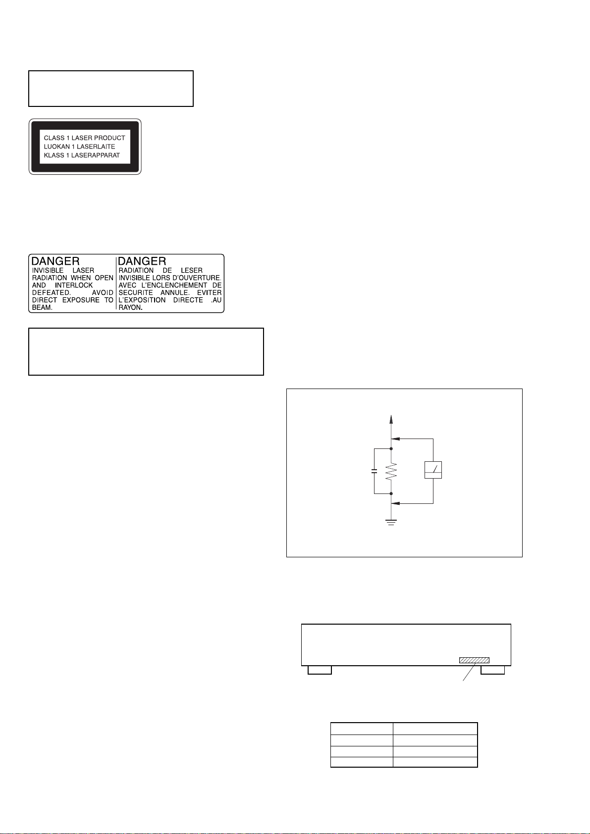
Laser component in this product is capable
of emitting radiation exceeding the limit for
Class 1.
This appliance is classified as a CLASS 1 LASER product. The
CLASS 1 LASER PRODUCT MARKING is located on the rear
exterior.
The following caution label is located inside the apparatus.
CAUTION
Use of controls or adjustments or performance of procedures
other than those specified herein may result in hazardous radiation
exposure.
Notes on chip component replacement
• Never reuse a disconnected chip component.
• Notice that the minus side of a tantalum capacitor may be
damaged by heat.
SAFETY CHECK-OUT
After correcting the original service problem, perform the
following safety checks before releasing the set to the customer:
Check the antenna terminals, metal trim, “metallized” knobs, screws,
and all other exposed metal parts for A C leakage. Check leakage as
described below.
LEAKAGE
The A C leakage from any e xposed metal part to earth ground and
from all exposed metal parts to any exposed metal part having a
return to chassis, must not exceed 0.5 mA (500 microamperes).
Leakage current can be measured by any one of three methods.
1. A commercial leakage tester, such as the Simpson 229 or RCA
WT -540A. Follo w the manufacturers’ instructions to use these
instruments.
2. A battery-operated AC milliammeter. The Data Precision 245
digital multimeter is suitable for this job.
3. Measuring the voltage drop across a resistor by means of a
VOM or battery-operated A C voltmeter . The “limit” indication
is 0.75 V, so analog meters must have an accurate low-volta ge
scale. The Simpson 250 and Sanwa SH-63Trd are e xamples of
a passive VOM that is suitable. Nearly all battery operated
digital multimeters that have a 2V AC range are suitable. (See
Fig. A)
To Exposed Metal
Parts on Set
Flexible Circuit Board Repairing
• Keep the temperature of soldering iron around 270˚C
during repairing.
• Do not touch the soldering iron on the same conductor of the
circuit board (within 3 times).
• Be careful not to apply force on the conductor when soldering
or unsoldering.
SAFETY-RELATED COMPONENT WARNING!!
COMPONENTS IDENTIFIED BY MARK 0 OR DOTTED LINE WITH
MARK 0 ON THE SCHEMATIC DIAGRAMS AND IN THE PARTS
LIST ARE CRITICAL TO SAFE OPERATION. REPLACE THESE
COMPONENTS WITH SONY PARTS WHOSE PART NUMBERS
APPEAR AS SHOWN IN THIS MANUAL OR IN SUPPLEMENTS
PUBLISHED BY SONY.
ATTENTION AU COMPOSANT AYANT RAPPORT
À LA SÉCURITÉ!
LES COMPOSANTS IDENTIFÉS P AR UNE MARQUE 0 SUR LES
DIAGRAMMES SCHÉMA TIQUES ET LA LISTE DES PIÈCES SONT
CRITIQUES POUR LA SÉCURITÉ DE FONCTIONNEMENT. NE
REMPLACER CES COMPOSANTS QUE PAR DES PIÈSES SONY
DONT LES NUMÉROS SONT DONNÉS DANS CE MANUEL OU
DANS LES SUPPÉMENTS PUBLIÉS PAR SONY.
0.15 µF
Fig. A. Using an A C v oltmeter to check A C leakage.
MODEL IDENTIFICATION
— BACK PANEL —
PARTS No. MODEL
4-238-401-0π
4-238-401-1π
4-238-401-3π
1.5 kΩ
Earth Ground
US
Canadian
E
AC
Voltmeter
(0.75 V)
Parts No.
2
Page 3

TABLE OF CONTENTS
RCD-W50C
Unleaded solder
Boards requiring use of unleaded solder are printed with the leadfree mark (LF) indicating the solder contains no lead.
(Caution: Some printed circuit boards may not come printed with
the lead free mark due to their particular size.)
: LEAD FREE MARK
Unleaded solder has the following characteristics.
• Unleaded solder melts at a temperature about 40°C higher than
ordinary solder.
Ordinary soldering irons can be used but the iron tip has to be
applied to the solder joint for a slightly longer time.
Soldering irons using a temperature regulator should be set to
about 350°C.
Caution: The printed pattern (copper foil) may peel away if the
heated tip is applied for too long, so be careful!
• Strong viscosity
Unleaded solder is more viscous (sticky, less prone to flow) than
ordinary solder so use caution not to let solder bridges occur such
as on IC pins, etc.
• Usable with ordinary solder
It is best to use only unleaded solder but unleaded solder may
also be added to ordinary solder.
1. SERVICING NOTE·····················································4
2. GENERAL ···································································5
3. DISASSEMBLY··························································6
3-1. Case (409538) ······························································· 7
3-2. Loading Panel (CDR) ··················································· 7
3-3. Front Panel Section······················································· 8
3-4. CD-SW Board, LED Board, DISPLAY Board ············· 8
3-5. CD Mechanism Deck (CDM65-RBD1) ······················· 9
3-6. Tray··············································································· 9
3-7. CDR Board ································································· 10
3-8. Holder (MG) Sub Assembly, Dust Cover ··················· 10
3-9. Optical Pick-Up (KRM-220CAA)······························ 11
3-10. Motor Assembly (Loading) (M201) ··························· 11
3-11. Cam (CH)···································································· 12
3-12. MAIN Board ······························································· 12
3-13. CD Mechanism Deck (CDM53L-30B61B) ················ 13
3-14. Fitting Base (Magnet) Assembly ································ 13
3-15. CLAMP MOTOR Board,
Motor (Clamp) Assembly (M701)······························ 14
3-16. Fitting Base (Guide) Assembly, Bracket (Chassis) ····· 14
3-17. Tray (Sub) ··································································· 15
3-18. Chassis (Mold B) ························································ 15
3-19. LOAD MOTOR Board,
Motor (Loading) Assembly (M702) ···························16
3-20. Stocker Section ··························································· 16
3-21. Slider (Selection), Tension Spring (Shutter),
Slider (Shutter)···························································· 17
3-22. Gear (Gear A), Gear (Gear B), Gear (U/D Slider)······ 17
Precaution During Gear (Gear U/D Slider),
Gear (Gear B), Gear (Gear A) Installation·················· 18
3-23. Gear (Chucking) ························································· 18
3-24. BD Board ···································································· 19
3-25. Optical Block Section ················································· 19
4. TEST MODE ···································································· 21
5. ELECTRICAL ADJUSTMENTS ······························· 24
CD SECTION ····························································· 24
CD-R/RW SECTION·················································· 25
6. DIAGRAMS······································································ 55
6-1. Block Diagrams – CD-R Section – ··························· 56
6-2. Printed Wiring Board – BD Section – ························ 59
6-3. Schematic Diagram – BD Section – ··························· 60
6-4. Printed Wiring Board
6-5. Schematic Diagram
6-6. Printed Wiring Board – CD-R Section (Side A) – ······ 63
6-7. Printed Wiring Board – CD-R Section (Side B) – ······ 64
6-8. Schematic Diagram – CD-R Section (1/4) – ·············· 65
6-9. Schematic Diagram – CD-R Section (2/4) – ·············· 66
6-10. Schematic Diagram – CD-R Section (3/4) – ·············· 67
6-11. Schematic Diagram – CD-R Section (4/4) – ·············· 68
6-12. Printed Wiring Board – MAIN Section (Side A) – ····· 69
6-13. Printed Wiring Board – MAIN Section (Side B) –····· 70
6-14. Schematic Diagram – MAIN Section (1/2) – ············· 71
6-15. Schematic Diagram – MAIN Section (2/2) – ············· 72
6-16. Printed Wiring Board – LED Section – ······················ 73
6-17. Schematic Diagram – LED Section – ························· 74
6-18. Printed Wiring Board – DISPLAY Section – ············· 75
6-19. Schematic Diagram – DISPLAY Section – ················ 76
6-20. IC Block Diagrams ····················································· 77
6-21. IC Pin Functions Description······································80
– CD Section – ······························· 57
– POWER/DISPLAY Section –······ 58
– SENSER/MOTOR/SW Section – ·····61
– SENSER/MOTOR/SW Section – ·····62
7. EXPLODED VIEWS ······················································ 54
7-1. Case Section··································································90
7-2. Front Panel Section ······················································· 91
7-3. Chassis Section ····························································· 92
7-4. Overall Section (CDM53L-30B61B)···························· 93
7-5.
Chassis (Mold) Assembly Section (CDM53L-30B61B) ··
7-6. Chassis Section (CDM53L-30B61B) ··························· 95
7-7. Optical Block Section ··················································· 96
7-8. CDM65-RBD1 ······························································ 97
94
8. ELECTRICAL PARTS LIST······································· 98
3
Page 4

RCD-W50C
SECTION 1
SERVICING NOTE
Self-diagnosis Function
When the self-diagnosis function is activated to
prevent the player from malfunctioning, three
character service numbers in a combination
with a message appears in the display. In this
case, check the following table.
Message
C12/
Cannot Copy
C13/
Rec Error
C14/
TOC Error
C41/
Cannot Copy
C71/
Din Unlock
Explanation
You are trying to record a disc that
cannot be played back in DECK-A
or with an external device, such as
CD-ROM or VIDEO CD.
• Remove the disc, and then insert a
music CD for playback.
Recording has not been completed
successfully because of vibration.
• Relocate the unit in a place free of
vibration and restart the recording
again.
The disc you try to record is
excessively dirty (such as oilstained or finger marked) or
scratched. Or the disc is not
normal.
• Replace the disc with another one
and restart the recording again.
The unit did not read the TOC
information.
• Insert other discs.
The sound source you are trying to
record is a copy of a commercial
music software. Or you are trying
to record on a CD-R/CD-RW
digitally.
• Because of the restriction of the
Serial Copy Management System,
you cannot record a copy of a
commercial music software.
Neither can you record a CD-R/
CD-RW digitally.
If this message is displayed
momentarily, this is not an error. It
is caused by the digital signal
during recording.
During recording of a digital sound
source, the connecting cable has
been disconnected or the player of
the sound source has turned off.
• Connect the cable or turn on the
digital player.
NOTES ON HANDLING THE OPTICAL PICK-UP BLOCK
OR BASE UNIT
The laser diode in the optical pick-up block may suffer electrostatic
break-down because of the potential difference generated by the
charged electrostatic load, etc. on clothing and the human body.
During repair, pay attention to electrostatic break-down and also
use the procedure in the printed matter which is included in the
repain parts.
The flexible board is easily damaged and should be handled with
care.
NOTES ON LASER DIODE EMISSION CHECK
The laser beam on this model is concentrated so as to be focused on
the disc reflective surface by the objective lens in the optical pickup block. Therefore, when checking the laser diode emission,
observe from more than 30 cm away from the objective lens.
The emission check enables continuous checking of the S curve.
LASER DIODE AND FOCUS SEARCH OPERATION
CHECK
Carry out the “S curve check” in “CD section adjustment” and check
that the S curve waveform is output three times.
4
Page 5
SECTION 2
GENERAL
RCD-W50C
2 5 978 q;
e;
wl
wgwh ws
1 POWER button
2 H button
3 DISC 1 to DISC 5 A button and indicators
4 CD SYNCHRO NORMAL button
3
41
qh PLAY MODE button
qj TIME button
qk DISPLAY button
ql YES button
6
qa
qs
qd
qgqhqjqkqlw;wd wawfwjwk
qf
5 CD SYNCHRO HIGH button
6 OPEN/CLOSE A button
7 H button
8 INPUT button
9 FINALIZE button
q; ERASE button
qa SBM button and indicator
qs REC z button
qd X button
qf REC LEVEL knob
qg x button
w; l AMS L knob
wa CLEAR button
ws MENU/NO button
wd l AMS L knob
wf CLEAR button
wg PLAY MODE button
wh TIME button
wj x button
wk PHONES jack
wl X button
e; PHONE LEVEL knob
5
Page 6
RCD-W50C
Note : Disassemble the unit in the order as shown below.
SECTION 3
DISASSEMBLY
SET
CASE (409538)
LOADING PANEL (CDR)
TRAY
CDR BOARD
HOLDER (MG) SUB ASSEMBLY, DUST COVER
MAIN BOARD
CD MECHANISM DECK (CDM53L-30B61B)
FITTING BASE (MAGNET) ASSEMBLY
MOTOR ASSEMBLY (LOADING) (M201)
FRONT PANEL SECTION
CD MECHANISM DECK (CDM65-RBD1)
CD-SW board, LED board, DISPLAY board
OPTICAL PICK-UP (KRM-220CAA)
CLAMP MOTOR BOARD, MOTOR (CLAMP) ASSEMBLY
CAM (CH)
FITTING BASE (GUIDE) ASSEMBLY,
BRACKET (CHASSIS)
BD BOARD
OPTICAL BLOCK SECTION
TRAY (SUB)
CHASSIS (MOLD B)
SLIDER (SELECTION), TENSION SPRING (SHUTTER),
SLIDER (SHUTTER)
GEAR (GEAR A), GEAR (GEAR B), GEAR(U/D SLIDER)
GEAR (CHUCKING)
LOAD MOTOR BOARD,
MOTOR (LOADING) ASSEMBLY
STOCKER SECTION
6
Page 7
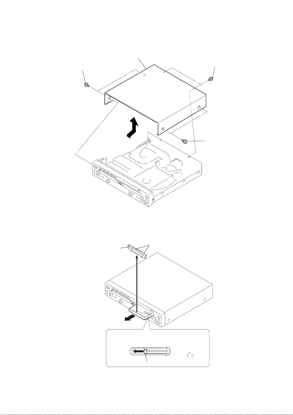
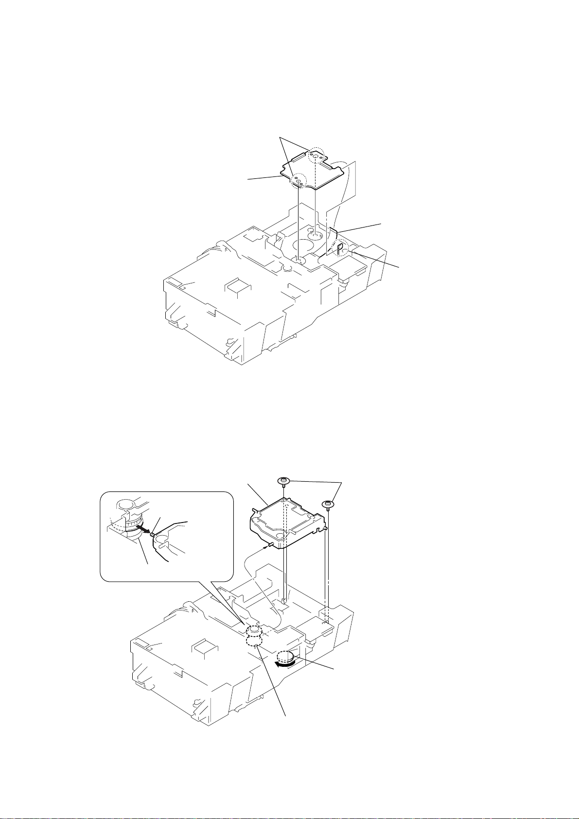
Note : Follow the disassembly procedure in the numerical order given.
3-1. Case (409538)
4
case (409538)
2
two
screws
(case 3 TP2 3
× 8
)
3
two
screws
(case 3 TP2 3
1
two
screws
(case 3 TP2 3
RCD-W50C
× 8
)
× 8
)
3-2. Loading Panel (CDR)
4
loading panel
two hooks
(CDR)
3
2
CD mechanism deck (CDM65-RBD1)
1
Slide the lever (cam (CH)) to the direction of arrow.
Front panel side
lever (cam (CH))
7
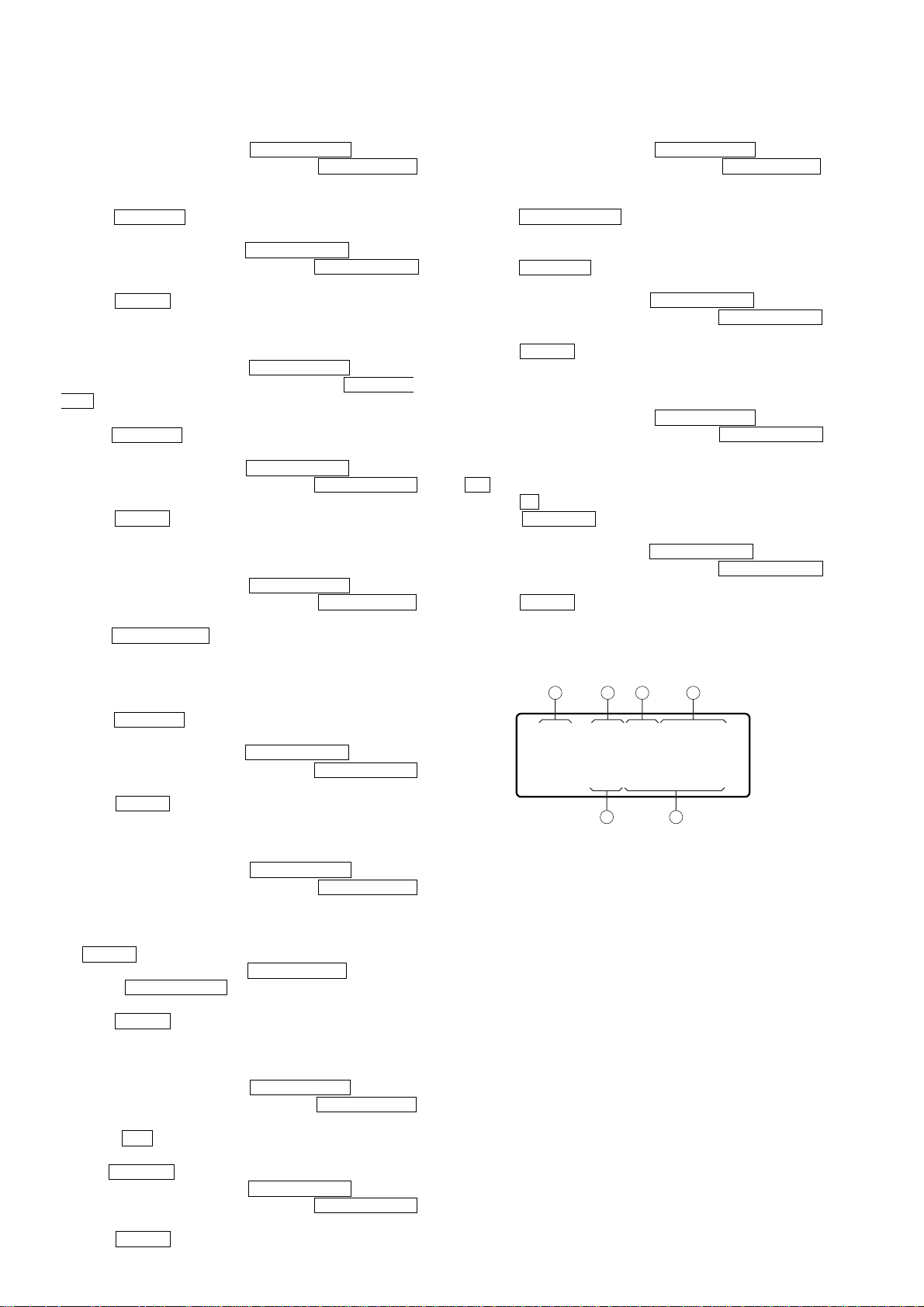
Page 8
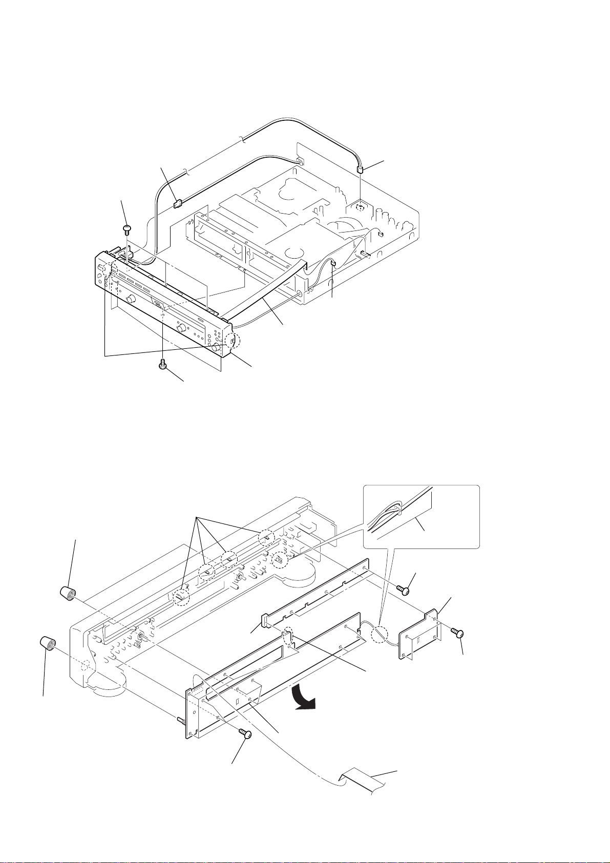
RCD-W50C
3-3. Front Panel Section
4
connector (2core)(CN920)
5
three
screws
(+BVTP 3
×
8)
1
connector (2core)(CN900)
2
connector (3core)(CN690)
7
t
wo claws
6
four screws
(+BVTP 3
×
8)
3-4. CD-SW Board, LED Board, DISPLAY Board
7
four
claws
2
two knobs (AMS)
3
flexible flat cable
(21core) (CN671)
8
front panel section
HARNESS PROCESSING
CD-SW board
5
three
screws
(+BVTP 2.6
×
4
CD-SW board
8)
1
8
knob (AMS)
9
LED board
6
twelve
(+BVTP 2.6
screws
qa
DISPLAY board
×
8)
8
Remove the soldering.
q;
flexible flat cable
(21core) (CN700)
3
four
screws
(+BVTP 2.6
×
8)
Page 9
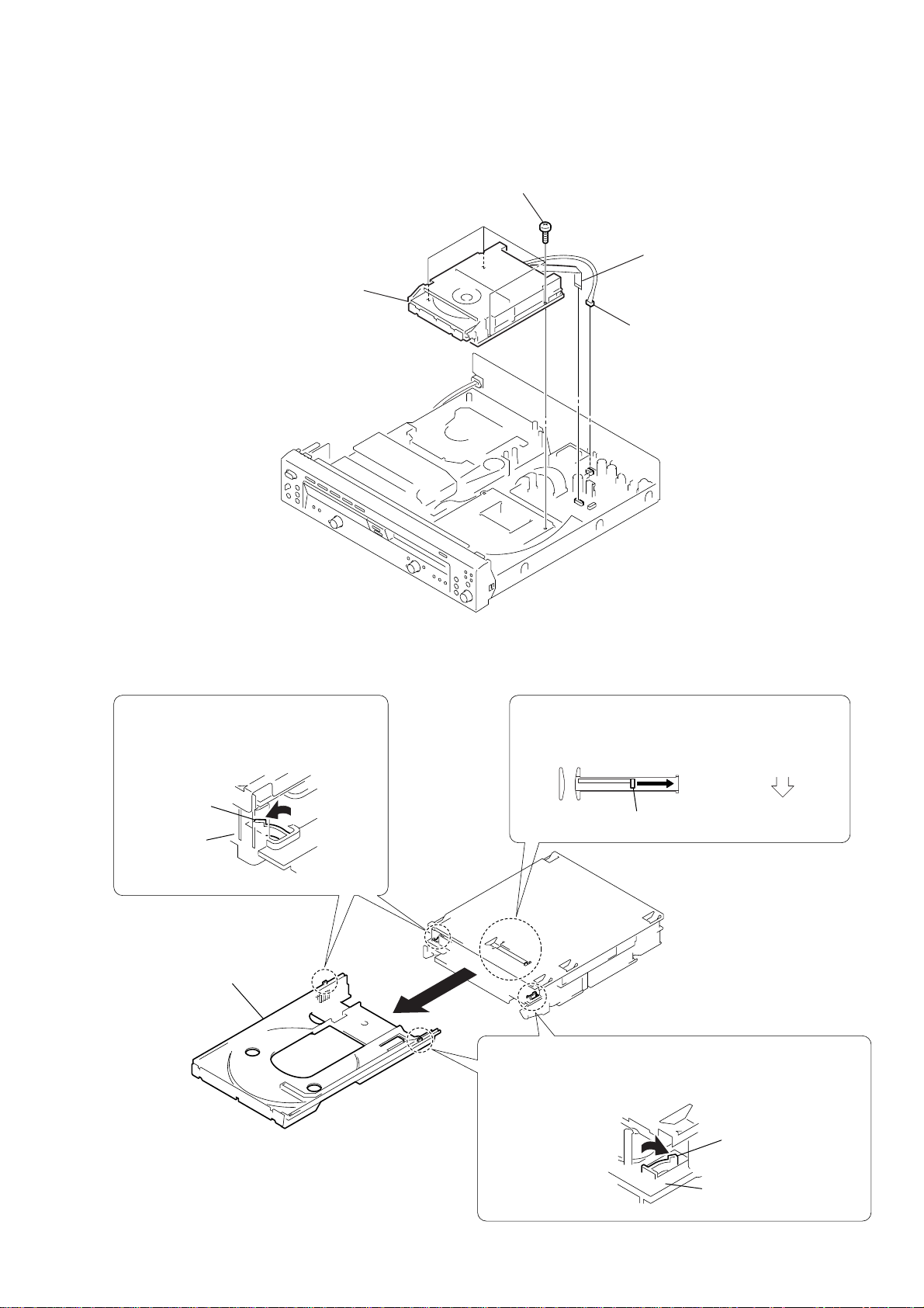
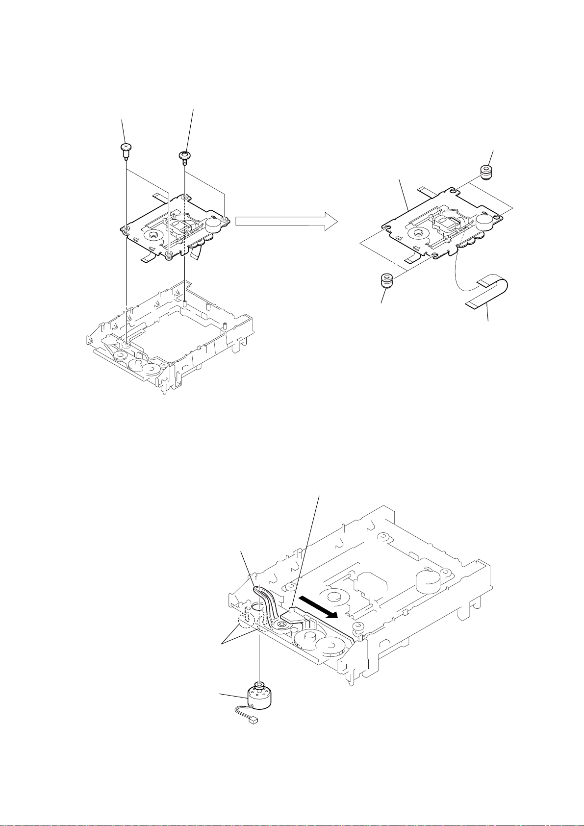
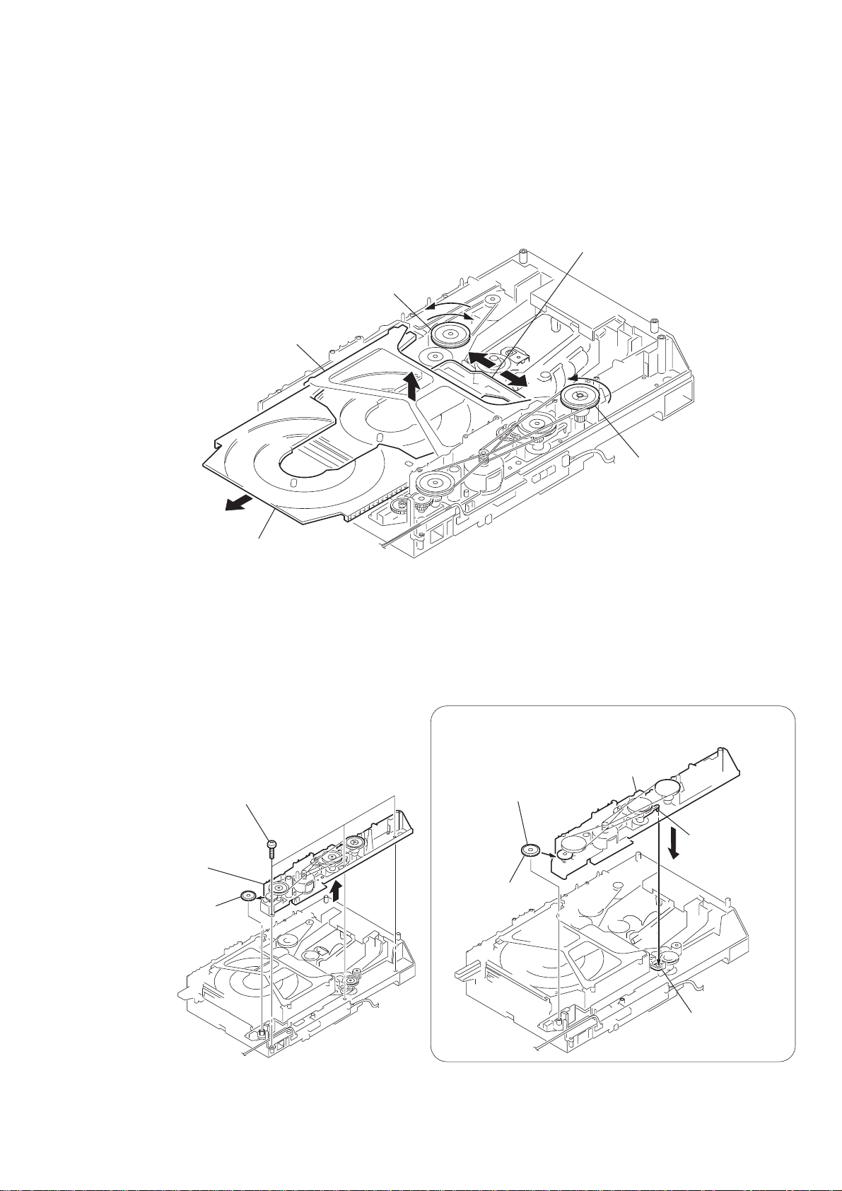
3-5. CD Mechanism Deck (CDM65-RBD1)
1
Slide the lever (cam (CH)) to the direction of arrow.
4
t
ray
2
Pull the tray while pressing the claw of
the chassis in the direction of the arrow.
3
Pull the tray while pressing the claw of the chassis and the claw
of the tray in the direction of the arrow.
front panel side
lever (cam (CH))
claw
claw
chassis
chassis
3
4
CD mechanism deck
(CDM65-RBD1)
four
screws (+BVTP 3
×
RCD-W50C
8)
2
flexible flat cable
(11core) (CN630)
1
connector
(CN631)
3-6. T ray
9
Page 10
RCD-W50C
r
3-7. CDR Board
2
bottom plate
9
CDR board
5
(11core) (CN103)
flexible flat cable
1
four
screws
(+BVTP 2.6
3
flexible flat cable
(32core) (CN101)
×
8)
6
c
law
8
c
onnector
(2 core) (CN104)
3-8. Holder (MG) Sub Assembly, Dust Cover
3
holder (MG)
sub assembly
1
two claws
4
flexible flat cable
(11core) (CN102)
7
c
law
4
three s
(+BVTP 2.6
crews
5
dust cove
×
8)
10
2
two claws
Page 11
3-9. Optical Pick-Up (KRM-220CAA)
)
2
1
two step screws
two screws
((2X9) (G with), +p tappin)
6
optical pick-up
(KRM-220CAA)
RCD-W50C
3
two insulators (main)
3-10. Motor Assembly (Loading) (M201)
2
Remove the belt (loading) from the
pulley of the motor assembly.
4
two insulators (main)
5
flexible flat cable
(32core) (from optical device
1
Slide the cam (CH) to the direction of arrow.
3
t
wo claws
4
m
otor assembly
(loading) (M201)
11
Page 12
RCD-W50C
)
3-11. Cam (CH)
5
holder (BU) sub assembly
1
1
1
2
Slide the cam (CH) to the
q;
direction of arrow
pressing the claw.
A
A
while
6
(+PTPWH 2.6
qs
cam (CH)
screw
7
×
8)
g
ear (C)
3-12. MAIN Board
1
4
qd
two
screws
(+BVTT 3
1
3
qs
(+BVTT 3
×
6)
cam (CH)
four
screws
× 6
claw
qa
)
qg
power transformer
8
claw
9
g
ear (B)
8
connector
(4core) (CN631)
6
connector
(2core) (CN900)
1
flexible flat cable
(21core) (CN671)
2
connector
(3core) (CN690)
7
flexible flat cable
(23core) (CN660)
5
flexible flat cable
(17core) (CN640)
4
connector
(5core) (CN641)
qf
Remove the soldering.
qh
MAIN board
9
screw
(+BVTP 3
3
flexible flat cable
(11core) (CN630)
×
8)
q;
bracket
qa
three
(+BVTP 3
(TR)
screws
×
8
12
Page 13
3-13. CD Mechanism Deck (CDM53L-30B61B)
2
four
screws (+BVTP 3
5
CD mechanism deck
(CDM53L-30B61B)
4
flexible flat cable
(17core) (CN701)
×
RCD-W50C
8)
1
connector
(CN641)
3
flexible flat cable
(23core) (CN101)
3-14. Fitting Base (Magnet) Assembly
3
fitting base (magnet)
assembly
2
four screws
(+BTTP M2.6 )
1
connector
(CN710)
13
Page 14
RCD-W50C
)
3-15. CLAMP MOTOR Board, Motor (Clamp) Assembly (M701)
1
belt (mode)
5
motor (clamp)
assembly (M701)
4
CLAMP MOTOR
board
2
two screws
(+BTTP M2.6)
3-16. Fitting Base (Guide) Assembly, Bracket (Chassis)
2
four screws
3
fitting base
(guide) assembly
1
two connectors
(CN709, 715)
(+BVTP 2.6
×
8)
4
two screws
(+BVTP 2.6
3
Remove the two solderings.
×
8)
6
bracket
(chassis)
5
three screws
(+BVTP 2.6
×
8
14
Page 15
3-17. T ray (Sub)
)
1
three screws
(+BTTP M2.6 )
2
Insert the gear (eject)
under the gear (LD
deceleration).
1
Insert the portion A of
chassis (mold B)
into the portion B of
slider (selection).
gear (eject)
portion A
portion B of
slider (selection)
3
g
ear (eject)
2
c
hassis (mold B)
chassis (mold B)
PRECAUTION DURING CHASSIS (MOLD B) INSTALLATION
1
Rotating the pulley (LD), shift the slider (selection) in the arrow A direction.
2
Rotating the pulley (mode) in the arrow direction, adjust the tray (sub) to be removed.
3
Rotating the pulley (LD), shift the slider (selection) in the arrow B direction.
4
Rotating the pulley (mode) in the arrow direction, remove the tray (sub) to be removed.
slider (selection)
pulley (LD)
RCD-W50C
stocker section
tray (sub)
3-18. Chassis (Mold B)
A
B
pulley (mode
15
Page 16
RCD-W50C
3-19. LOAD MOTOR Board, Motor (Loading) Assembly (M702)
1
belt (communication)
2
3
belt (loading1)
belt (loading1)
7
motor (loading)
assembly (M702)
6
LOAD MOTOR
board
3-20. Stocker Section
2
two step screws
4
two screws
(+BTTP M2.6)
4
stocker section
5
Remove the two solderings.
PRECAUTION DURING STOCKER
SECTION INSTALLATION
Hook the portion A of tray (SUB)
to the slider (selection).
portion A
of tray (SUB)
sticking of
slider (selection)
16
1
gear (gear A)
3
two step screws
Page 17
3-21. Slider (Selection), Tension Spring (Shutter), Slider (Shutter)
)
1
two floating screws
(+PTPWHM 2.6 x 6)
2
4
slider (selection),
tension spring (shutter),
slider (shutter)
washer
3
compression
spring (gear)
RCD-W50C
PRECAUTION DURING SLIDER
(SELECTION) INSTALLATION (2)
Insert the slider (selection)
into the portion A.
portion A
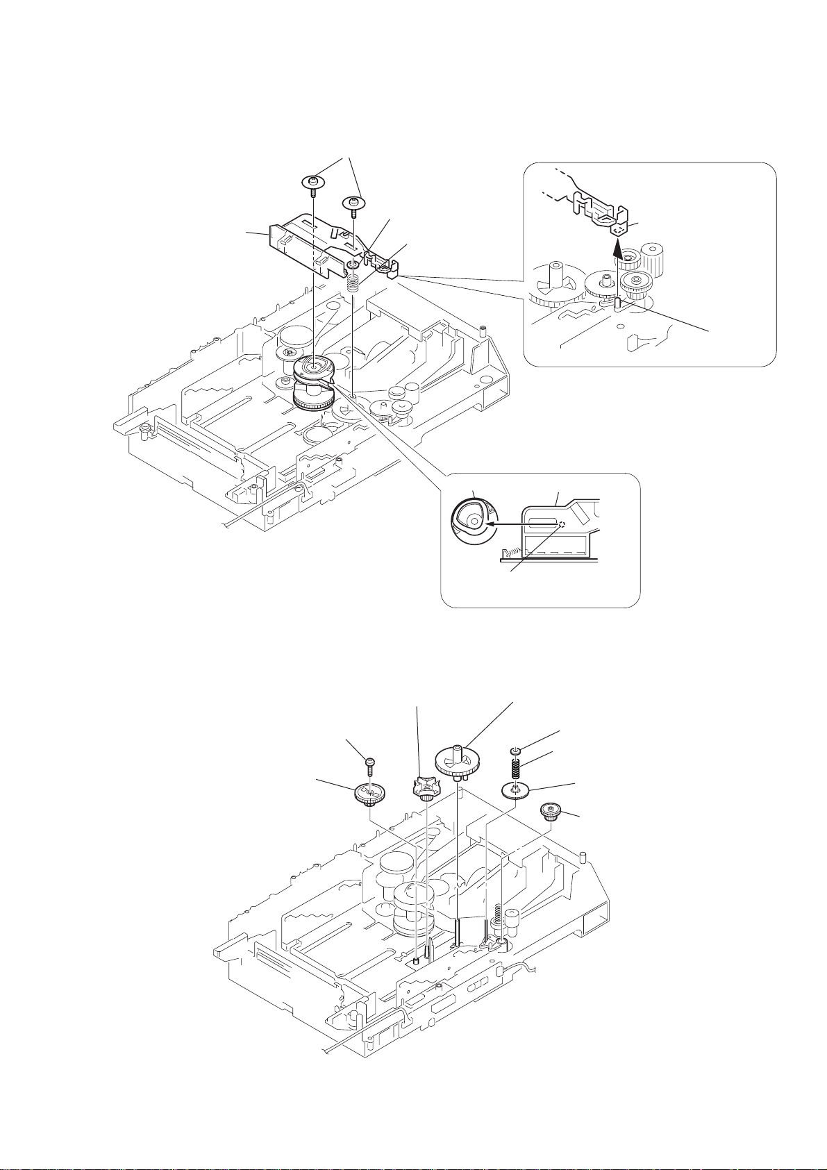
3-22. Gear (Gear A), Gear (Gear B), Gear (U/D Slider)
6
gear (gear B)
7
screw
(+BTTP M2.6)
8
gear (U/D slider)
PRECAUTION DURING SLIDER
(SELECTION) INSTALLATION (1)
gear (chuking)
Insert a convex portion into
the groove of gear (chucking).
slider (selection)
5
gear (gear A)
3
2
washer
compression spring
4
gear (selection
1
gear (relay)
17
Page 18
RCD-W50C
Precaution During Gear (Gear U/D Slider), Gear (Gear B), Gear (Gear A) Installation
3
gear (gear B)
portion A
Adjust the gear (gear B) with the
portion A as shown.
slider (U/D)
1
Slide the slider (U/D)
fully in the arrow
direction.
4
2
gear (U/D slider)
slider (U/D) gear
gear (gear A)
gear
(gear B)
linearly
Adjust the gear so that it meshes with
the bottom tooth of slider (U/D) gear,
as shown.
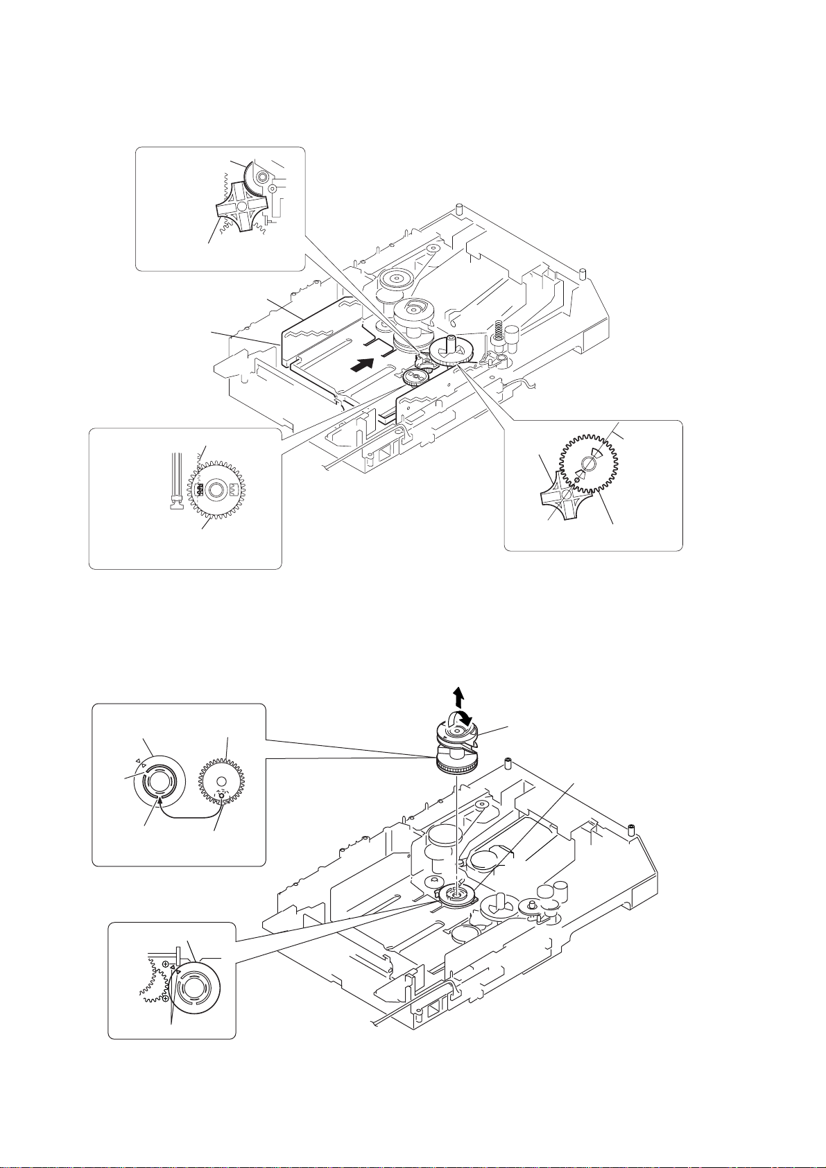
3-23. Gear (Chucking)
PRECAUTION DURING
GEAR (CHUCKING) (2)
rotary encoder
(S707)
NG
OK
Align with the slot of
rotary encoder.
PRECAUTION DURING
GEAR (CHUCKING) (1)
rotary encoder (S707)
gear
(chucking)
2
1
Adjust so as to be aligned with
gear B linearly, as shown.
3
gear (chucking)
rotary encoder (S707)
18
Align marking.
Page 19
3-24. BD Board
2
Remove soldering from the four points.
4
BD board
1
flexible flat cable
(16core) (CN102)
3
hook
RCD-W50C
3-25. Optical Block Section
4
3
shaft (BU holder)
gear (chucking)
optical block section
2
1
two floating screws
(+PTPWHM 2.6)
Rotate the pulley (LD) in the direction of 2 to move
the shaft (BU holder) upper.
gear (chucking)
19
Page 20

RCD-W50C
MEMO
20
Page 21

SECTION 4
TEST MODE
RCD-W50C
Setting the Test Mode
Procedure:
1. Press the POWER button to POWER on.
2. Pr ess the l AMS L (DECK A), [SBM] and l AMS
L (DECK B) buttons in order without releasing the button.
3. Turn the l AMS L (DECK B) knob to select the men u.
4. Pr ess the l AMS L (DECK B) knob to execute the test
mode.
Releasing the Test Mode
Procedure 1:
1. Turn the l AMS L (DECK B) knob to select the Ship
Mode.
2. Pr ess the l AMS L (DECK B) knob to execute the Ship
Mode.
3. Press the POWER button to POWER off.
Procedure 2:
1. Pr ess the l AMS L (DECK A), [SBM] and l AMS
L (DECK B) buttons in order without releasing the button.
2. Press the POWER button to POWER off.
Contents of test mode
No. Display Function
1 SYS Version System version display
2 CDR Version CDR version display
3BU Test Deck A BU test mode
4 SERVICE Deck A Service mode
5 Ship Mode CD Shipment mode
6 FL ALL ON Fluorescent indicator tube test
7 FL ALL OFF Fluorescent indicator tube test
8 FL ITIMATSU Fluorescent indicator tube test
9 LED CHECK LED check
10 KEY CHECK Keyboard check
11 RM CHECK Remote commander check
12 CDR History CDR error history display
13 Play Speed Deck A x4 speed
System Version Display
Procedure:
1. Enter the test mode, then turn the l AMS L (DECK B)
knob to display “SYS Version”, and press the l AMS L
(DECK B) knob.
2. The system version is displayed.
3. To exit from this mode, turn the l AMS L (DECK B)
knob to display “Ship Mode”, and press the l AMS L
(DECK B) knob to execute the Ship Mode.
4. Press the POWER button to POWER off.
CDR Version Display
Procedure:
1. Enter the test mode, then turn the l AMS L (DECK B)
knob to display “CDR Version”, and press the l AMS L
(DECK B) knob.
2. The CDR version is displayed.
3. To exit from this mode, turn the l AMS L (DECK B)
knob to display “Ship Mode”, and press the l AMS L
(DECK B) knob to execute the Ship Mode.
4. Press the POWER button to POWER off.
BU Test Mode (Deck A)
Procedure:
1. Enter the test mode, then turn the l AMS L (DECK B)
knob to display “BU Test”, and press the l AMS L
(DECK B) knob.
2. “bdt S CURVE” is displayed. This test mode is used in the Electrical Adjustment section.
3. T urn the l AMS L (DECK B) knob. “bdt RAM READ”,
“bdt RAM WRITE”, “bdt COMOUT”, “bdt FB TUNE” and “bdt
ERR RATE” are displayed.
4. To exit from this mode, press the MENU/NO button and turn
the l AMS L (DECK B) knob to display “bdt ERR
RATE”.
5. Press the l AMS L (DECK A), [SBM] and l AMS
L (DECK B) buttons in order without releasing the button.
6. Press the POWER button to POWER off.
Service Mode (Deck A)
Procedure:
1. Enter the test mode, then turn the l AMS L (DECK B)
knob to display “SERVICE”, and press the l AMS L
(DECK B) knob.
2. “SERVICE MODE” is displayed.
3. Press the ERASE button, the “SLED OUT” is displayed and
the sled moves to the outermost position.
4. Press the FINALIZE button, the “SLED IN” is displayed and
the sled moves to the innermost position.
5. Press the l AMS L (DECK B) knob, then “SERVICE
MODE” is displayed again.
6. To exit from this mode, press the l AMS L (DECK A),
[SBM] and l AMS L (DECK B) buttons in order with-
out releasing the button.
7. Press the POWER button to POWER off.
Note: Always move the pick-up to the most inside position when
exiting from this mode.
Ship Mode
Procedure:
1. Enter the test mode, then turn the l AMS L (DECK B)
knob to display “Ship Mode”, and press the l AMS L
(DECK B) knob.
2. “Push POWER!” is displayed.
3. Press the POWER button to POWER off.
FL ALL ON Mode
Procedure:
1. Enter the test mode, then turn the l AMS L (DECK B)
knob to display “FL ALL ON”, and press the l AMS L
(DECK B) knob.
2. All segments of fluorescent indicator tube and all LEDs turn on.
3. Press the MENU/NO button, then “FL ALL ON” is displayed
again.
4. To exit from this mode, turn the l AMS L (DECK B)
knob to display “Ship Mode”, and press the l AMS L
(DECK B) knob to execute the Ship Mode.
5. Press the POWER button to POWER off.
21
Page 22
RCD-W50C
FL ALL OFF Mode
Procedure:
1. Enter the test mode, then turn the l AMS L (DECK B)
knob to display “FL ALL OFF”, and press the l AMS L
(DECK B) knob.
2. All segments of fluorescent indicator tube and all LEDs turn off.
3. Press the MENU/NO button, then “FL ALL OFF” is displayed
again.
4. To exit from this mode, turn the l AMS L (DECK B)
knob to display “Ship Mode”, and press the l AMS L
(DECK B) knob to execute the Ship Mode.
5. Press the POWER button to POWER off.
FL ITIMATSU Mode
Procedure:
1. Enter the test mode, then turn the l AMS L (DECK B)
knob to display “FL ITIMATSU”, and press the l AMS
L (DECK B) knob.
2. Checkered patterns of segments are displayed.
3. Press the MENU/NO button, then “FL ITIMATSU” is displayed
again.
4. To exit from this mode, turn the l AMS L (DECK B)
knob to display “Ship Mode”, and press the l AMS L
(DECK B) knob to execute the Ship Mode.
5. Press the POWER button to POWER off.
LED Check Mode
Procedure:
1. Enter the test mode, then turn the l AMS L (DECK B)
knob to display “LED CHECK”, and press the l AMS L
(DECK B) knob.
2. Turn the l AMS L (DECK A) or (DECK B) knob clock-
wise. The green LED (DISC 1) turns on, then the orange LED
(DISC 1) turns on. The each orange LED turns on after the green
LED from DISC 1 to DISC 5. The LED (SBM) turns on at last.
Counterclockwise rotation gives a performance in re verse order .
3. Press the MENU/NO button, then “LED CHECK” is displayed
again.
4. To exit from this mode, turn the l AMS L (DECK B)
knob to display “Ship Mode”, and press the l AMS L
(DECK B) knob to execute the Ship Mode.
5. Press the POWER button to POWER off.
KEY Check Mode
Procedure:
1. Enter the test mode, then turn the l AMS L (DECK B)
knob to display “KEY CHECK”, and press the l AMS L
(DECK B) knob.
2. “Got l keys” is displayed.
3. Press the buttons, and when all the buttons are pressed (without
the POWER button), “Got 36 keys” will be displayed.
4. To exit from this mode, press the l AMS L (DECK A),
[SBM] and l AMS L (DECK B) buttons in order with-
out releasing the button.
5. Press the POWER button to POWER off.
Remote Commander Check
Procedure:
1. Enter the test mode, then turn the l AMS L (DECK B)
knob to display “RM CHECK”, and press the l AMS L
(DECK B) knob.
2. Press the H key on the remote commander, then “Got
PlayCom” is displayed.
Press the MENU/NO button, then “RM CHECK” is displayed again.
3.
4. To exit from this mode, turn the l AMS L (DECK B)
knob to display “Ship Mode”, and press the l AMS L
(DECK B) knob to execute the Ship Mode.
5. Press the POWER button to POWER off.
CDR History Display
Procedure:
1. Enter the test mode, then turn the l AMS L (DECK B)
knob to display “CDR History”, and press the l AMS L
(DECK B) knob.
2. “00 ######## ########” is displayed as the first error hitory.
3. Turn the l AMS L (DECK B) knob to select the error
history. The number of error histories is ten in all.
(Refer to “Contents of CDR error history”.)
4. Press the MENU/NO button, then “CDR History” is displayed
again.
5. To exit from this mode, turn the l AMS L (DECK B)
knob to display “Ship Mode”, and press the l AMS L
(DECK B) knob to execute the Ship Mode.
6. Press the POWER button to POWER off.
Play Speed Selection Mode (Deck A)
Procedure:
1. Enter the test mode, then turn the l AMS L (DECK B)
knob to display “Play Speed”, and press the l AMS L
(DECK B) knob.
2. “x4 Play” is displayed. If a CD is in the deck A, pressing the
H button executes the 4 times speed playback.
3. Press the x button to stop the playback.
4. Press the MENU/NO button, then “Play Speed” is displayed
again.
5. To exit from this mode, turn the l AMS L (DECK B)
knob to display “Ship Mode”, and press the l AMS L
(DECK B) knob to execute the Ship Mode.
6. Press the POWER button to POWER off.
Contents of CDR error history
display(example)
1 2
3 4
00 05070D80
000E2E0D
5 6
(hexadecimal)
1 Order of the error history
00 to 09: ten error histories in all
2 Error contents
01: unable to focus on
02: Q code/ATIP discontinuous (several frames preceding)
03: Q code/ATIP unreadable
04: search taking more than sixteen seconds
05: focus failure
06: sled over run
07: not passing by start time to write
08: audio buffer over
09: sync failure
OA: Spindle lock taking more than 8 secouds
example : 05 is focus failure
22
Page 23

RCD-W50C
3 Operation mode
bit 7: Speed
0: normal speed
1: x4 speed
bit 6 to bit 0: Number of inner condition
01: POWER off condition/during shift to POWER on
02: POWER off and shipment setting/during shift to POWER
off and shipment setting
03: stop condition/during stop
04: during start up of servo
05: during TOC reading and others
06: during CD TEXT reading
07: during standby(waiting for command from the CD sys-
tem)/during search
08: during playback
09: during manual search(playback)
0A:during pause
0B:during manual search(pause)
0C:during OPC
0D:recording standby/during recording pause
(enable to shift to recording)
0E: during recording
0F: unable to record (waiting for shift to being recordable)
10: PMA updating
11: during operation of unfinalize
12: during operation of finalize
13: PMA erasing
14: emergency
15: recording preparation
16: recording end
5 Write POWER (integer of mW x 10, availab le during write
processing)
examples: 00 means unavailable
(when 3 operation mode is not recording)
: A3 means 163(decimal), i.e. 16.3 mW
6 ATIME (min)/(sec)/(frame)
example: 0E, 2E, 0D means 14 : 46 : 13
Abbreviations:
ATIP : Absolute Time In Pre-groove
OPC : Optimum POWER Control
PMA : Program Memory Area
examples :
bit
HEX
77654 321
0000 0111
07
00
1001 0001
91
11 1
4 Start time of read in(compression method)
bit 15 to bit 13 : (min)
0: 97 min
1: 96 min
2: 95 min
7: others
bit 12 to bit 7: (sec)
bit 6 to bit 0: (frame)
examples :
HEX
bit
0 Operation mode
normal speed, during
standby(waiting for
command from the CD
system)/during search
during operation of
0000 1101 1000 0000
0D,80
97(min) 27(sec)
x4 speed,
unfinalize
7
654 321
0(frame)
015 14 13 12 11 10 9 8 Start time of read in
97 : 27 : 00
11,16
0001 0001 0001 0110
34(sec)97(min) 22(frame)
97 : 34 : 22
23
Page 24
RCD-W50C
)
e
p
e
+
–
BD board
TP (TE)
TP (DVC)
oscilloscope
(DC range)
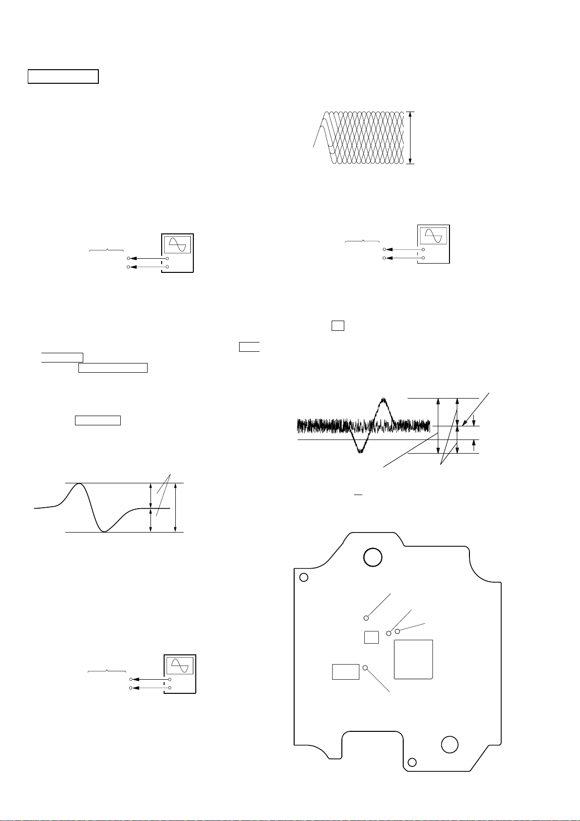
SECTION 5
ELECTRICAL ADJUSTMENTS
CD SECTION (DECK A)
Note :
1. CD Block is basically designed to operate without adjustment.
Therefore, check each item in order given.
2. Use YEDS-18 disc (3-702-101-01) unless otherwise indicated.
3. Use an oscilloscope with more than 10MΩ impedance.
4. Clean the object lens by an applicator with neutral detergent
when the signal level is low than specified value with the
following checks.
S Curve Check
Connection :
oscilloscop
(DC range)
BD board
TP (FE)
TP (DVC)
Procedure :
1. Connect an oscilloscope to test point TP (FE) and TP (DVC) on
the BD board.
2. Turn the power on.
3. Load the disc (YEDS-18).
4. Enter the test mode, select the BU Test asd press the l
AMS L (DECK B) knob to display “bdt S CURVE”.
5. Press the l AMS L (DECK B) knob. “LD AL” is
displayed and playback starts automatically.
6. Check the oscilloscope waveform (S-curve) is symmetrical
between A and B. And confirm peak to peak level within 3.6 ±
0.5 Vp-p.
7. Press the MENU/NO button to stop playback.
8. Exit from the test mode.
(Refer to the TEST MODE Section)
+
–
Note: A clear RF signal waveform means that the shape “◊” can be
clearly distinguished at the center of the waveform.
VOLT/DIV : 200mV
TIME/DIV : 500ns
level : 1.1 ± 0.3Vp-p
E-F Balance (1 Track jump) Check
Connection :
Procedure:
1. Connect an oscilloscope to TP (TE) and TP (DVC).
2. Turn the power on.
3. Load the disc (YEDS-18) and playback the number five track.
4. Press the X (DECK A) button.
(Becomes the 1 track jump mode.)
5. Confirm the level B and A (DC voltage) on the oscilloscope
waveform.
Center of
waveform
B
0V
A (DC voltage
symmetry
A
within 3.6
B
VOLT/DIV : 1V
TIME/DIV : 2ms
±
0.5 Vp-
Note: Try to measure several times to make sure than the ratio of A
: B or B : A is more than 10 : 7.
RF Level Check
Connection :
oscilloscop
(AC range)
BD board
TP (RFAC)
TP (DVC)
+
–
Procedure :
1. Connect an oscilloscope to TP (RFAC) and TP (DVC).
2. Turn the power on.
3. Load the disc (YEDS-18) and playback the number five track.
4. Confirm that oscilloscope waveform is clear and check RF signal
level is correct or not.
24
level=1.1 ±0.6Vp-p
Specification level: x 100=less than ±22%
A
B
Symmetry
[BD BOARD] — SIDE A —
TP (DVC)
TP (TE)
TP (FE)
IC104
IC101
IC103
TP (RFAC)
Page 25
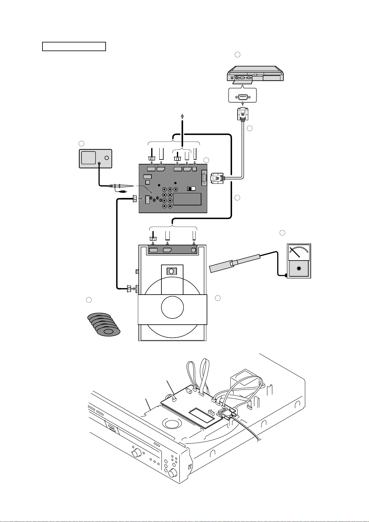
CD-R/RW SECTION
*The following is the method of locating the faulty point and
electrical adjustment.
1. Connection and Setting of Programs
PC
3
(w/ SerialI/F)
RCD-W50C
1-1. Connection
5
Oscilloscope
(A)
MPXOUT
To
RCD-W50C
(B) (C) (D)
0-756-358-11
CDM65-RBD1 SERVICE
RESET
Jig
CONTROL FIRM
(B) (C) (D)
COM1
8
RS-232C
Jig
2
9
Cables for Jig connecting
Cable
6
Laser Power
Meter
7
Test Disc
CDM65-RBD1
jig
1
CDM65-RBD1
4 Fig. Position of Jig (Set the jig after removing the cover of CDM65-RBD1)
25
Page 26
RCD-W50C
1-2. Equipments to prepare
1 Test Object Both RBD1 and CDM65-RBD1 shall be tested.
RBD1 : Flash Memory Writing of of
Circuit Test by Self-diagnostics
CDM65-RBD1 : Electrical Adjustment
Performance Test
2 Jig (With 9 Cables, Parts No.J-2501-223-A)
3 PC Windows95/98/2000/Me with COMport (RS-232C)
4 Programs TeraTerm Pro + Service macro
5 Oscilloscope More than 150MHz
6 Laser Power Meter LEADER LPM-8001 (Parts No.J-2501-046-A)
7 Test Disc
PATD-012 : (Parts No.4-225-203-1) Adjustment for Playback (CD,CD-R)
TCD-W091W : (Parts No.J-2501-226-A) Adjustment for Playback (CD-RW)
CRM74 (Blank CD-R) : Adjustment and Check for Recording (CD-R)
CWM74 (Blank CD-RW) : Check for Recording (CD-RW)
TCD-W032W : (Parts No.J-2501-227-A) Defocus tolerance (CD-RW)
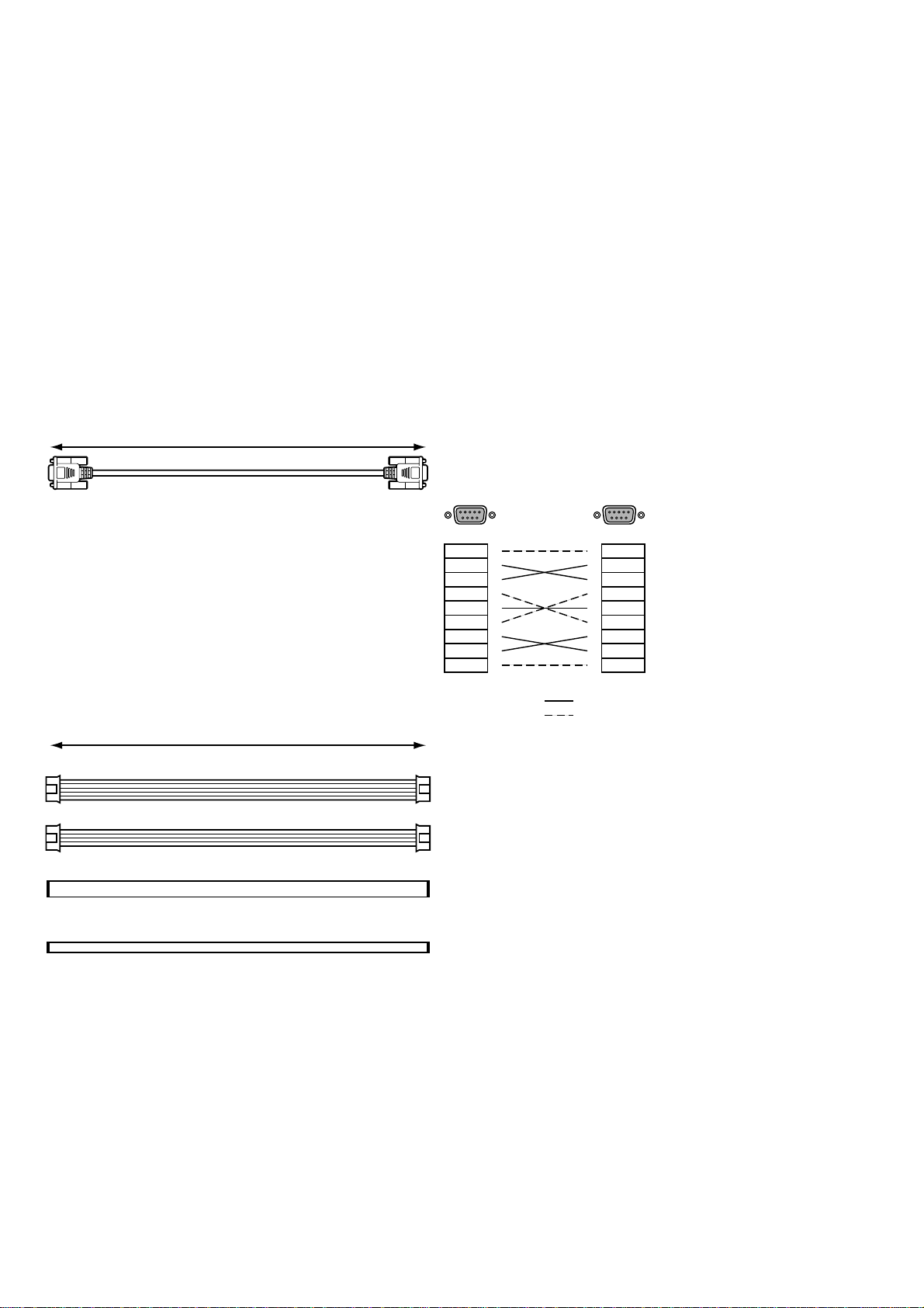
8 RS-232C Cable
L=2000mm
(E)
D-sub 9pin Female cross cable
54321
9876
1
2
3
4
5
6
7
8
9
54321
9876
1
2
3
4
5
6
7
8
9
9 Cables for Jig connecting
:mandatory
: not use
L=300mm
(A)
PH 5p
(B)
PH 4p
(C)
FFC 11p 1.0mm pitch (J-2501-200-A)
(D)
FFC 5p 1.0mm pitch (J-2501-212-A)
26
Page 27
1-3. Setting of Programs (Tera Term Pro and Service macro)
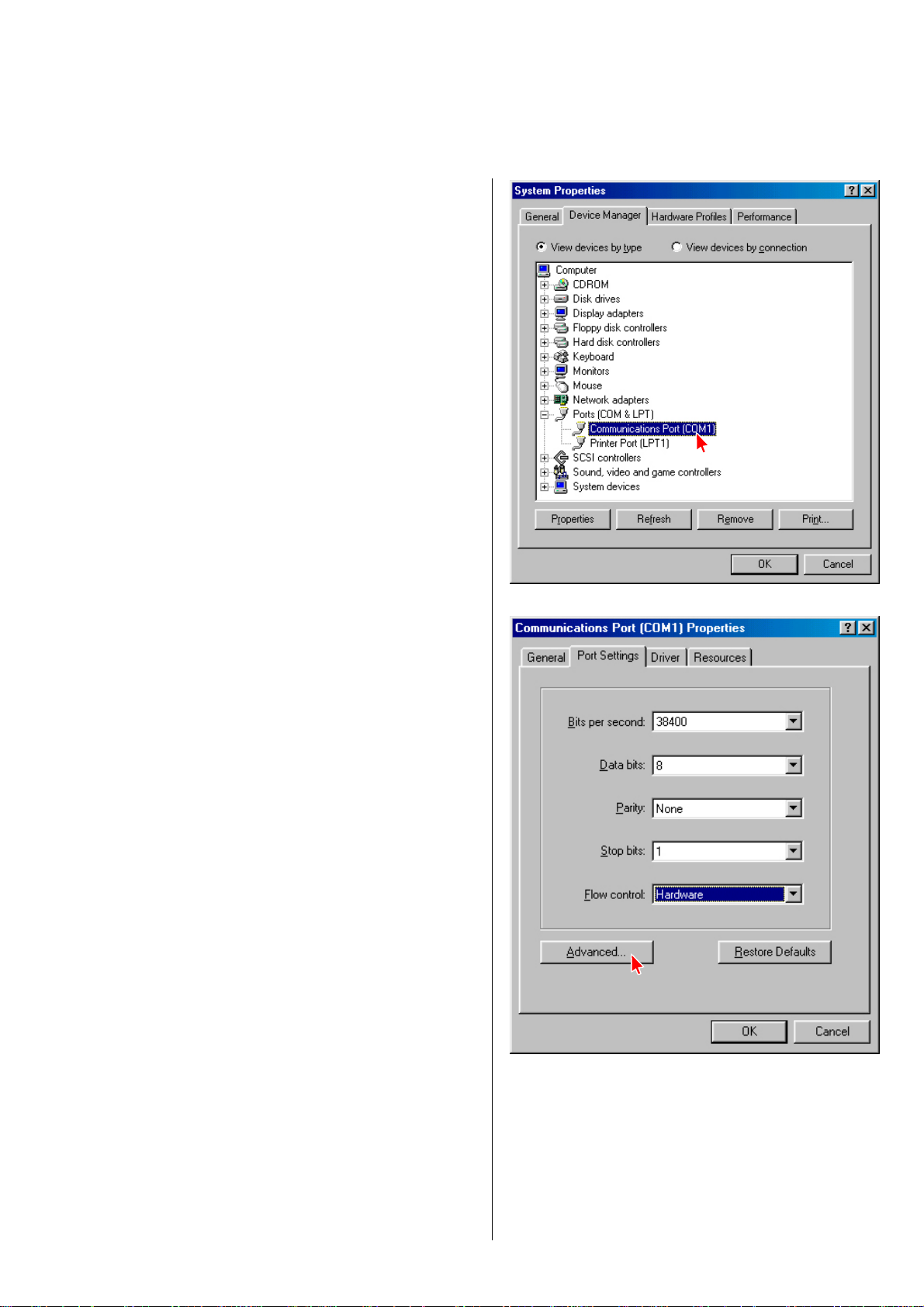
* Confirmation of System (Windows 98 is used in this explanation) Preparation for Terminal software
1) Set up the serial port from OS.
a) Select Start → Settings → Control Panel and select System →
Device manager → Communication Port (COMn)
(see Fig. 1-1)
* Specify the COM port that connected with JIG of CDM65.
RCD-W50C
b) Double click COMn (as you connect to the Jig-CDM65)
Set the parameters as below.
Bits per second : 38400
Data bits : 8
Parity : non
Stop bits : 1
Flow control : hardware
(see Fig.1-2)
4 Fig. 1-1
4 Fig. 1-2
27
Page 28
RCD-W50C
Ver 1.1 2003.12
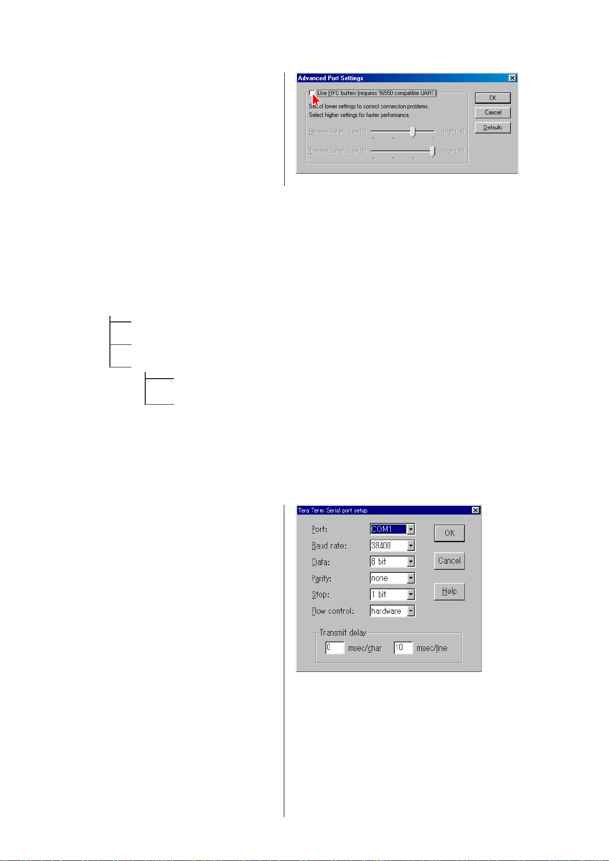
c) Press “Advanced...” button (see Fig.1-2)
Remove the check “Use FIFO buffers ...”
(see Fig.1-3)
4 Fig. 1-3
2) Unzip the file “ttermp23.zip” by PC.
(The file “ttermp23.zip” is distributed together with the service manual.)
3) After unzip the files, you can find setup.exe.
Double click the setup.exe.
Please install as the installer is.
Do not change the directory that files are installed. (use default)
4) Unzip the file “files-0208.zip” by PC.
Copy all “ttl” file and “FUNC” folder which are contained in “files-0208” and paste them in the “Ttermpro” file as below.
(The file “files-0208.zip” is distributed together with the service manual.)
Ttermpro
01ldp_S.ttl
...
10vwdcC_S.ttl
FUNC
AMS.ttl
...
VERCHK.ttl
4 Fig. 1-4
Note : Do not change the directory path.
5) Start-up the TeraTermPro
Double click the ttermpro.exe.
6) Set up the TeraTermPro (IMPORTANT!!)
a) Select Setup → Serial Port... and set the parameters as below.
Port : (As you connect to the Jig-CDM65)
Baud rate : 38400
Data : 8 bit
Parity : none
Stop : 1 bit
Flow control : hardware
Transmit delay : 0 msec/char 10 msec/line
After settings, press “OK” button. (see Fig.1-5)
28
4 Fig. 1-5
Page 29
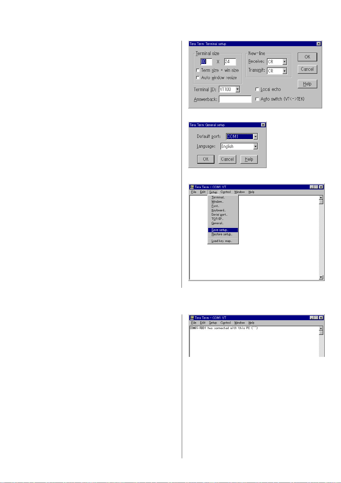
b) Terminal setup
Set the parameters as below.
New-line receive : CR
transmit : CR
After settings, press “OK” button. (see Fig.1-6)
c) General setup
Select the language and press “OK” button. (see Fig.1-7)
RCD-W50C
4 Fig. 1-6
4 Fig. 1-7
d) Saving the setup
Select Setup → Save setup... and save as teraterm.ini in the
Ttermpro directory. (see Fig.1-8)
7) Connect the JIG and CDM65.
8) Confirm the S510 on JIG is ‘CONTROL’.
9) Power on the CDM65 and press SW101(RESET) on JIG.
“CDM65-RBD1 has connected with this PC (^^)” is displayed.
(see Fig.1-9)
If above message is not displayed, you may hav e some mistakes.
Please confirm previous setting procedures again.
4 Fig. 1-8
4 Fig. 1-9
29
Page 30
RCD-W50C
2.
Repair Works That Require Electrical Adjustment
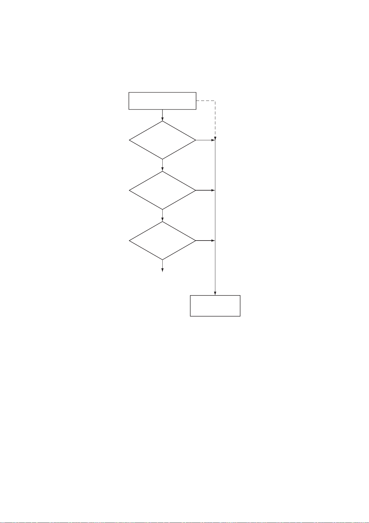
In the case of repair works as shown below, electrical adjustment is required.
Locating the faulty point
KRM-220CAA
is replaced.
No
RBD1
is replaced.
No
The parts shown
in the List (1)
is replaced.
No
Electrical adjustment
is not required.
Yes
Yes
Yes
Electrical adjustment
30
List (1) : IC101, IC103, IC171, IC201, IC502
Page 31

3. Locating the Faulty Point
3-1. Laser Power Check
1) Select the menu as follows. Control → Macro, and select
LDPtestL_S.ttl.
Press “Open”. (Fig. 3-1, 3-2)
RCD-W50C
4 Fig. 3-1
4 Fig. 3-2
2) Press the “RESET” button (SW101) of the jig as prompted by the display.
3) Place probe of a laser power meter in the specified position
following the display as shown in Fig. 3-3. (See Fig. 3-3-a)
4 Fig. 3-3
sensor probe
CDM65-RBD1
jig
optical pick-up
4 Fig. 3-3-a
Note : Do not add stress to an optical pick-up.
31
Page 32

RCD-W50C
4) When the display shown in Fig. 3-4 appears, set the Range of a
laser power meter to “1 mW” and press “OK”.
5) Check that the laser power meter reading satisfies the following
requirement. When the laser power satisfies the required
specification, press “OK”. (Fig. 3-5)
LEADER LPM-8001 : 0.76 to 0.86 mW
4 Fig. 3-4
6) When the display shown in Fig. 3-6 appears, set the Range of a
laser power meter to “10 mW” and press “OK”.
7) Check that the laser power meter reading satisfies the following
requirement. When the laser power satisfies the required
specification, press “OK”. (Fig. 3-7)
LEADER LPM-8001 : 4.5 to 4.7 mW
4 Fig. 3-5
4 Fig. 3-6
4 Fig. 3-7
8) Check that the laser power meter reading satisfies the following
requirement. When the laser power satisfies the required
specification, press “OK”. (Fig. 3-8)
LEADER LPM-8001 : 9.2 to 9.6 mW
32
4 Fig. 3-8
Page 33

9) Check that the message “Power Check End” appears on display .
(Fig. 3-9)
If the measurement result is outside the specification value,
either perform section 4. CDM65-RBD1 Electrical Adjustment
(see page 39), or locate the cause of the error by performing
the Laser Deterioration Judgment.
3-2. Laser Deterioration Judgment
1) Select the menu as follows. Control → Macro, and select
10vwdcC_S.ttl.
Press “Open”. (Fig. 3-10, 3-11)
RCD-W50C
4 Fig. 3-9
4 Fig. 3-10
4 Fig. 3-11
2) Press the “RESET” button (SW101) of the jig as prompted by the display.
3) When the message [OK] appears as shown in Fig. 3-12, press
the “OK” button.
When the laser unit KRM-220CAA (Op) is normal without
deterioration of laser, the message [OK] appears. If the laser
unit is deteriorated, the message [NG] appears. Then, replace
the laser unit KRM-220CAA (Op).
4 Fig. 3-12
33
Page 34

RCD-W50C
4) Check that the message “CDRW VWDC-CHECK completed!”
appears. (Fig. 3-13)
NG Judgment Result Indication
When the present VWDC value of the laser unit KRM-220CAA
(Op) does not satisfy the required specification, the message
“VWDC (Line End - Now) [NG]” appears.
Measure: Check the peripheral of CN101.
Replace KRM-220CAA.
4 Fig. 3-13
3-3. Use of Self Diagnosis Function-1 (In the case when result data of the past electrical adjustment, is not needed.)
Perform the self diagnosis as described below in the case when electrical adjustment is not performed yet, or when result data of the
electrical adjustment in the past, is not needed and ready to be erased.)
1) Connect the CDM65-RBD1 (abbreviated as CDM65 hereafter) that is going to be repaired, the jig and a PC following the Connection
Diagram as shown in section 1-1.
2) Turn on the power of the RCD-W50C in which the CDM65 is installed.
3) Start up the TeraTermPro that is installed in PC. Set the switch S510 on the jig to “CONTROL”.
4) Press the “RESET” button (SW101) of the jig. (Fig. 3-14)
4 Fig. 3-14
5) Type portchk [Enter] from keyboard of PC. (Fig. 3-15)
Note 5-1 : When the KRM-220CAA is connected, the spindle
motor rotates at a high speed. If the message “H8/
3064 Port Check END!” appears, press the “RESET”
button and stop the spindle.
Note 5-2 : When the CDM65 (loading mechanism) is installed,
ignore the message “PA (#93-100): NG”.
Confirm that “OK” is displayed in all items except for the cases
as described above.
If “NG” is displayed in any item, it is assumed that the pin
number of IC501 as shown in Fig. 3-15 is defective or its
peripheral has abnormality. Perform the repair wor k again and
repeat the self diagnosis. Repeat the repair work and self
diagnosis until OK is displayed.
34
4 Fig. 3-15
Page 35

6) Type diagno [Enter] from keyboard of PC.
Note 6-1 : When the KRM-220CAA is connected, the spindle
motor rotates at a high speed. If the message
“Diagnosis END!” appears, press the “RESET”
button and stop the spindle.
Note 6-2: When the KRM-220CAA is connected (i.e. when
the FFC for optical laser unit is connected to CN101
is connected), ignore the message “ AK8567 (w/o OP)
check: NG”.
Confirm that “OK” is displayed in all items except for the cases
as described above.
If “NG” is displayed in any item, it is assumed that the point
indicated by the item in Fig. 3-16 is defective or its peripheral
has abnormality . Perform the repair work a gain and repeat the
self diagnosis. Repeat the repair work and self diagnosis until
“OK” is displayed.
7) Perform the operation check.
3-4. Use of Self Diagnosis Function-2
(In the case when result data of the past electrical adjustment, should be left saved.)
4 Fig. 3-16
RCD-W50C
Perform the self diagnosis as described below in the case when the faulty point could not be identified e ven after completion of the repair
work that is defined as “The repair work in which electrical adjustment is not required” in section “2. Repair Works That Require
Electrical Adjustment”.
1) Select the menu as follows. Control → Macro, and select
E2bkupF.ttl.
Press “Open”. (Fig. 3-17, 3-18)
4 Fig. 3-17
4 Fig. 3-18
35
Page 36

RCD-W50C
2) Type the filename in which result of electrical adjustment is
going to be saved. Press “OK”. (Fig. 3-19)
3) Confirm that the message “completed!” appears.
The EEPROM data is backed up. (Fig. 3-20)
4 Fig. 3-19
4 Fig. 3-20
4) Perform step 1) through step 6) of section “3-3. Use of Self Diagnosis Function-1”.
5) Select the menu as follows. Control → Macro, and select E2recvF.ttl.
Press “Open”.
6) Press the “RESET” button (SW101) of the jig as prompted by
the display. (Fig. 3-21)
4 Fig. 3-21
7) Type the filename in which result of electrical adjustment is
saved. Press “OK”. (Fig. 3-22)
36
4 Fig. 3-22
Page 37

8) Confirm that the message “completed!” appears.
The EEPROM data is recovered. (Fig. 3-23)
4 Fig. 3-23
9) Perform the operation check.
3-5. Acquisition of Error History and Acquisition of Elapsed Operating Hours
RCD-W50C
Check if error has occurred or not by performing the following steps. If error has occurred, it is interpreted and saved in the specific
directory. Check contents of the error by viewing the specific directory as described below.
1) Select the menu as follows. Control → Macro, and select
ErrHistGetAll_S.ttl.
Press “Open”. (Fig. 3-24, 3-25)
4 Fig. 3-24
4 Fig. 3-25
37
Page 38

RCD-W50C
2) Press the “RESET” button (SW101) of the jig as prompted by the display.
3) When there is no error, the display as shown in Fig. 3-26
appears.
4 Fig. 3-26
4) When error has occurred, the display as shown in Fig. 3-27
appears showing error history. Contents of the errors are
displayed as shown in Fig. 3-28 after interpretation of the error
log. Check the contents of the error by looking at the file
“EEPROM_Errorlog.txt” in the TeraTermPro directory
5) The elapsed operating hours is shown at the top of
“EEPROM_Errorlog.txt” regardless of presence/absence of the
error history. Check the elapsed operating hours from the
display as shown in Fig. 3-28.
4 Fig. 3-27
SN = xxxx
Op elapsed time: 12:0:56
Spindle elapsed time: 17:9:44
**** Error Log data(0) ****
Error Pointer= 38
Error Code= 05,04,E0,00,00,01,0D,0D
Focus is dropped
1x speed
Servo wakeup
Lead In Start Time= 7:0:0
Laser Power= 0
ATIME= 1:13:13
**** Error Log data(-1) ****
Error Pointer= 30
Error Code= 05,04,E0,00,00,00,14,43
Focus is dropped
1x speed
Servo wakeup
Lead In Start Time= 7:0:0
Laser Power= 0
ATIME= 0:20:67
38
4 Fig. 3-28 : Error log example
Page 39

4. CDM65-RBD1 Electrical Adjustment
4-1. Laser Power Adjustment
1) Start up the TeraTermPro and set the switch S510 on the jig to “CONTROL”.
2) Select the menu as follows. Control → Macro, and select
01ldp_S.ttl.
Press “Open”. (Fig. 4-1)
4 Fig. 4-1
RCD-W50C
3) Press the “RESET” button (SW101) of the jig as prompted by the display.
4) Press the “RESET” button (SW101) of the jig again as prompted by the display.
5) When the display as shown in Fig. 4-2 appears, type the serial
number (see Fig. 4-3) that is printed on the label attached to
the RBD1. (This dialog appears only when the EEPROM IC502
is replaced.)
4 Fig. 4-2
4 Fig. 4-3
When the display as shown in Fig. 4-4 appears, press “No”.
When the display as shown in Fig. 4-5 appears after that, press
“Yes”.
4 Fig. 4-4
4 Fig. 4-5
39
Page 40

RCD-W50C
6) When the display as shown in Fig. 4-6 appears, place the probe
of the laser power meter on top of the optical laser unit, and
press “OK”. (See Fig. 3-3-a, page 31)
7) When the display as shown in Fig. 4-7 appears, set the Range
of a laser power meter to “1 mW” and press “OK”.
8) Adjust the laser output power as follows.
The laser output power (i.e., laser power meter reading) should
satisfy the specification shown below.
LEADER LPM-8001 : 0.81 +/- 0.05 mW (0.76 to 0.86 mW)
*To increase the laser output power
Press [Yes] of the “Up?” dialog box.
*To decrease the laser output power
Press [No] of the “Up?” dialog box and then press [Y es] of the
“Down?” dialog box.
4 Fig. 4-6
4 Fig. 4-7
Repeat until the laser output power satisfies the specification.
(Fig. 4-8, 4-9)
*When the setting value is determined
Press [No] of the “Up?” dialog box
and then press [No] of the “Down?” dialog box
and press [Yes] of the “Save?” dialog box. (Fig. 4-10)
9) When the display shown in Fig. 4-11 appears, set the Range of
a laser power meter to “10 mW” and press “OK”.
4 Fig. 4-8
4 Fig. 4-9
4 Fig. 4-10
4 Fig. 4-11
40
Page 41

10) Adjust the laser output power as follows.
The laser output power (i.e., laser power meter reading) should
satisfy the specification shown below.
LEADER LPM-8001 : 4.6 +/- 0.1 mW (4.5 to 4.7 mW)
*To increase the laser output power
Press [Yes] of the “Up?” dialog box.
*To decrease the laser output power
Press [No] of the “Up?” dialog box
and then press [Yes] of the “Down?” dialog box.
Repeat until the laser output power satisfies the specification.
(Fig. 4-12, 4-13)
RCD-W50C
4 Fig. 4-12
*When the setting value is determined
Press [No] of the “Up?” dialog box
and then press [No] of the “Down?” dialog box
and press [Yes] of the “Save?” dialog box. (Fig. 4-14)
11) Adjust the laser output power as follows.
The laser output power (i.e., laser power meter reading) should
satisfy the specification shown below.
LEADER LPM-8001 : 9.4 +/- 0.2 mW (9.2 to 9.6 mW)
*To increase the laser output power
Press [Yes] of the “Up?” dialog box.
*To decrease the laser output power
Press [No] of the “Up?” dialog box
and then press [Yes] of the “Down?” dialog box.
Repeat until the laser output power satisfies the specification.
(Fig. 4-15, 4-16)
4 Fig. 4-13
4 Fig. 4-14
4 Fig. 4-15
*When the setting value is determined
Press [No] of the “Up?” dialog box
and then press [No] of the “Down?” dialog box
and press [Yes] of the “Save?” dialog box. (Fig. 4-17)
4 Fig. 4-16
4 Fig. 4-17
41
Page 42

RCD-W50C
12) When the display shown in Fig. 4-18 appears, remov e probe of
the laser power meter and press OK.
13) Check that the message “Laser Power CAL completed!”
appears. (Fig. 4-19)
NG Judgment Result Indication
4 Fig. 4-18
4 Fig. 4-19
4-1-1. Sled Speed NG!
Contents : This message appears when the movement performance of sled is outside the specification.
Measure : Check if there is any abnormality in the sled drive circuit (IC171 peripheral) and the sled drive mechanism.
4-1-2. Power CAL NG!
Contents : This message appears when the laser emission intensity is outside the specification.
Measure : Check peripheral of CN101.
Replace KRM-220CAA.
4-2. CD/CD-R Playback Adjustment
1) Select the menu as follows. Control → Macro, and select 02cdr_S.ttl.
Press “Open”.
2) Place the test CD disc PATD-012 on the tray as prompted by
the display and press “OK”. (Fig. 4-20)
4 Fig. 4-20
3) Press the “RESET” button (SW101) of the jig as prompted by the display.
4) As prompted by the message shown in Fig. 4-21, check that
the waveform as sho wn in Fig. 4-22 appears on an oscilloscope.
42
4 Fig. 4-21
Page 43

Note :The clear RF signal waveform means that the shape “ ” can be clearly distinguished at the center of the waveform.
RF signal waveform
VOLT/DIV : suitable value
TIME/DIV : 500ns
4 Fig. 4-22
5) As prompted by the message shown in Fig. 4-24, check that
the waveform as sho wn in Fig. 4-23 appears on an oscilloscope.
RF signal waveform
VOLT/DIV : suitable value
TIME/DIV : 500ns
RCD-W50C
4 Fig. 4-23
6) As prompted by the message shown in Fig. 4-26, check that
the waveform as sho wn in Fig. 4-25 appears on an oscilloscope.
RF signal waveform
VOLT/DIV : suitable value
TIME/DIV : 500ns
4 Fig. 4-25
7) Check that the message “CDR PB-CAL completed!” appears.
NG Judgment Result Indication
4-2-1. Playback Measurement NG!
4 Fig. 4-24
4 Fig. 4-26
Contents : This message appears when the BLER (Block Error Rate) during playback is outside the specification.
Measure : Check if there is any abnormality in RBD1.
Replace KRM-220CAA.
43
Page 44

RCD-W50C
4-3. CD-RW Playback Adjustment
1) Select the menu as follows. Control → Macro, and select 03cdr_S.ttl.
Press “Open”.
2) Place the test CD TCD-W091W on the tray as prompted by
the display and press “OK”. (Fig. 4-27)
4 Fig. 4-27
3) Press the “RESET” button (SW101) of the jig as prompted by the display.
4) As prompted by the message shown in Fig. 4-29, check that
the waveform as sho wn in Fig. 4-28 appears on an oscilloscope.
RF signal waveform
VOLT/DIV : suitable value
TIME/DIV : 500ns
4 Fig. 4-28
5) As prompted by the message shown in Fig. 4-31, check that
the waveform as sho wn in Fig. 4-30 appears on an oscilloscope.
RF signal waveform
VOLT/DIV : suitable value
TIME/DIV : 500ns
4 Fig. 4-30
6) As prompted by the message shown in Fig. 4-33, check that
the waveform as sho wn in Fig. 4-32 appears on an oscilloscope.
RF signal waveform
VOLT/DIV : suitable value
TIME/DIV : 500ns
4 Fig. 4-29
4 Fig. 4-31
44
4 Fig. 4-32
4 Fig. 4-33
Page 45

7) Check that the message “CDRW PB-CAL completed!” appears.
(Fig. 4-34)
RCD-W50C
NG Judgment Result Indication
4-3-1. Playback Measurement NG!
Contents: This message appears when the BLER (Block Error Rate) during playback is outside the specification.
Measure : Check if there is any abnormality in RBD1.
Replace KRM-220CAA.
4-4. CD-R Recording Adjustment and Self Record/Playback Check
1) Select the menu as follows. Control → Macro, and select 04cdr_S.ttl.
Press “Open”.
2) Place the test CD disc PATD-012 on the Deck A. Place the
recording CD-R disc (see Note: 4-4-1) on the tray (Deck B) as
prompted by the display and press “OK”. (Fig. 4-35)
Note : 4-4-1
The disc to be used in this step.
* Use the CD-R disc CRM74 for audio, that is manufactured by
Sony.
* The disc that is used by this step cannot be used for the general
purposes and for the purpose of operation check of the RCD
series equipment. The disc that is used for the general purposes
or for the purpose of operation check of the RCD series
equipment, cannot be used in this step.
* If the recording is interrupted by any reasons during the
recording operation (i.e., the WRITE POWER ON LED of the
jig is lighting), the disc cannot be used any more in the
subsequent step. Use the un-used brand new disc and repeat
this step from the very beginning again.
4 Fig. 4-34
4 Fig. 4-35
3) When the disc that is used in step 2) is the disc that has been
used in the electrical adjustment in the past........ Press “Yes”.
When the disc that is used in step 2) is a completely blank disc.
...... Press “No”. (Fig. 4-36)
Note: The recording CD-R disc can be used only for the
electrical adjustment. The recording CD-R disc must be
controlled so that it must not be used for any other
applications.
4 Fig. 4-36
45
Page 46

RCD-W50C
4) Press the H button of Deck A. After playback starts, press
“OK”. (Fig. 4-37)
5) When the message as shown in Fig. 4-38 appears some seconds
later, select 4x of the test mode (refer to page 22, Play Speed
Selection Mode (Deck A)) PLAYBACK SPEED. Then press
the H button of Deck A. After playback starts, press “OK”.
6) As prompted by the message shown in Fig. 4-40, check that
the waveform as sho wn in Fig. 4-39 appears on an oscilloscope.
RF signal waveform
VOLT/DIV : suitable value
TIME/DIV : 500ns
4 Fig. 4-37
4 Fig. 4-38
4 Fig. 4-39
7) As prompted by the message shown in Fig. 4-42, check that
the waveform as sho wn in Fig. 4-41 appears on an oscilloscope.
RF signal waveform
VOLT/DIV : suitable value
TIME/DIV : 500ns
4 Fig. 4-41
8) Check that the message “CDR REC-CHECK completed!” appears.
NG Judgment Result Indication
4-4-1. CD-R Playback Measurement NG!
4 Fig. 4-40
4 Fig. 4-42
Contents : This message appears when the BLER (Block Error Rate) *Beta/m11 of the track that is recorded and played back, is outside
the specification.
Measure : Check if there is any abnormality in RBD1.
Replace KRM-220CAA.
46
Page 47

4-5. CD-RW Recording Adjustment and Self Record/Playback Check
1) Select the menu as follows. Control → Macro, and select 05cdrw_S.ttl.
Press “Open”.
2) Place the test CD disc PATD-012 on the Deck A. Place the
recording CD-RW disc (see Note: 4-5-1) on the tray (Deck
B) as prompted by the display and press “OK”. (Fig. 4-43)
RCD-W50C
Note : 4-5-1
The disc to be used in this step.
* Use the CD-RW disc CWM74 for audio, that is manufactured
by Sony.
* The disc that is used by this step cannot be used for the general
purposes and for the purpose of operation check of the RCD
series equipment as it is. The disc that is used for the general
purposes or for the purpose of operation check of the RCD
series equipment, cannot be used in this step.
When you want to use the CD-R W disc for other applications,
erase the CD-RW disc.
* If the recording is interrupted by any reasons during the
recording operation (i.e., the WRITE POWER ON LED of the
jig is lighting), the disc cannot be used any more in the
subsequent step. In such a case, erase the CD-RW disc and
repeat this step from the very beginning again.
3) When the disc that is used in step 2) is the disc that has been
used in the electrical adjustment in the past........ Press “Yes”.
When the disc that is used in step 2) is a completely blank disc.
......... Press “No”. (Fig. 4-44)
Note : The recording CD-RW disc can be used only for the
electrical adjustment. The recording CD-R W disc must
be controlled so that it must not be used for any other
applications.
4 Fig. 4-43
4 Fig. 4-44
4) Press the H button of Deck A. After playback starts, press
“OK”. (Fig. 4-45)
5) When the message as shown in Fig. 4-46 appears some seconds
later, select 4x of the test mode (refer to page 22, Play Speed
Selection Mode (Deck A)) PLAYBACK SPEED. Then press
the H button of Deck A. After playback starts, press “OK”.
4 Fig. 4-45
4 Fig. 4-46
47
Page 48

RCD-W50C
6) As prompted by the message shown in Fig. 4-48, check that
the waveform as sho wn in Fig. 4-47 appears on an oscilloscope.
RF signal waveform
VOLT/DIV : suitable value
TIME/DIV : 500ns
4 Fig. 4-47
4 Fig. 4-48
7) As prompted by the message shown on display, check that the waveform as shown in Fig. 4-49 appears on an oscilloscope.
RF signal waveform
VOLT/DIV : suitable value
TIME/DIV : 500ns
4 Fig. 4-49
8) Check that the message “CDRW REC-CHECK completed!”
appears. (Fig. 4-50)
NG Judgment Result Indication
4 Fig. 4-50
4-5-1. CD-RW Playback Measurement NG!
Contents : This message appears when the BLER (Block Error Rate) *Beta/m11 of the track that is recorded and played back, is outside
the specification.
Measure : Check if there is any abnormality in RBD1.
Replace KRM-220CAA.
48
Page 49

4-6. VWDC Check
1) Select the menu as follows. Control → Macro, and select 06vwdc_S.ttl.
Press “Open”.
2) As prompted by the message shown in Fig. 4-51, remove the
disc from the tray and press “OK”.
4 Fig. 4-51
3) Because this step saves the result of electrical adjustment in a
file, there can be a case that the dialog as shown in Fig. 4-52
appears.
When you want to overwrite.....................Press “Yes”.
When you want to create a new file..........Press “No”.
4 Fig. 4-52
4) Check that the message “CDRW VWDC-CHECK completed!”
appears. (Fig. 4-53)
RCD-W50C
NG Judgment Result Indication
4 Fig. 4-53
4-6-1. EEPROM Write NG!
Contents : This message appears when writing data into EEPROM fails.
Measure : When the steps of 01ldp_S.ttl through 05cdrw_S.ttl have no problem and the error occurs only in this step, it is assumed that
an error has occurred momentarily in the interface between PC and CDM65. Therefore, repeat execution of 06vwdc_S.ttl
again.
4-6-2. VWDC judge [Line Top - End] [NG]
Contents : This message appears when the VWDC value is outside the specification.
Measure : It is assumed that the optical laser unit has deteriorated. If this error occurs after the KRM-220CAA is replaced, the adjustment
error in the step of 01ldp_S.ttl is assumed. Therefore, repeat execution of steps of 01ldp_S.ttl through 05cdrw_S.ttl again. In
the cases other than above, check if the laser power adjustment is correctly performed or not, using LDPtestL_S.ttl.
49
Page 50

RCD-W50C
4-7. NG Message List
Message Cause
Tray OPEN NG! The tray has not opened within the specified time.
Tray Close NG! The tray has not closed within the specified time.
SLEDIN NG! The sled has not moved toward inner circumference within the specified time.
SLEDOUT NG! The sled has not moved toward outer circumference within the specified time.
RIDR NG! The RID information could not be read out within the specified time.
SNread (1) NG! The SN (1) information could not be read out within the specified time.
SNread (2) NG! The SN (2) information could not be read out within the specified time.
SNread (3) NG! The SN (3) information could not be read out within the specified time.
FBIASADJ NG! The Focus Bias Adjustment has not completed within the specified time.
FEOSADJ NG! The FE Offset Adjustment has not completed within the specified time.
FESAMPADJ NG! The FE Amplitude Adjustment has not completed within the specified time.
RFACCHK NG! The RFAC amplitude is abnormal or the adjustment has not completed within the specified time.
RPINWADJ1 NG! The Read Power (during Write1) Adjustment has not completed within the specified time.
RPINWADJ2 NG! The Read Power (during Write2) Adjustment has not completed within the specified time.
SERVOSET NG! The Servo Setting has not completed within the specified time.
TSa NG! The ATIME Search has not completed within the specified time.
PLAYSW NG! The Play operation has not started within the specified time.
STOP NG! The Stop operation has not completed within the specified time.
AMS NG! The AMS operation has not completed within the specified time.
ATIPPLAY NG! The ATIP Play operation has not started within the specified time.
END TNO get NG! The record-end track information could not be obtained within the specified time.
LEADOUT info.get NG! The record-end time information could not be obtained within the specified time.
Invalid EndTrackNo./LeadoutTime ! The illegal record-end track and its time information were obtained.
Use the Blank disc The disc exceeding the allowable limit is used.
DIR unlock! The equipment could not be synchronized with the signal connected to DIN2.
RWP NG! The CD-R Write Power setting has not completed within the specified time.
RWWP NG! The CD-RW Write Power setting has not completed within the specified time.
REC NG! The record operation could not be started within the specified time.
50
Page 51

5. Operation Check
5-1. Erasing the Error History
1) Select the menu as follows. Control → Macro, and select
ErrHistClear.ttl.
Press “Open”. (Fig. 5-1, 5-2)
RCD-W50C
4 Fig. 5-1
4 Fig. 5-2
2) Press the “RESET” button (SW101) of the jig as prompted by the display.
3) Check that the message “completed!” appears. (Fig. 5-3)
4 Fig. 5-3
51
Page 52

RCD-W50C
5-2. Playback Check using TCD-W032W
1) Install the CDM65 in the equipment and install the TCD-W032W in Deck B.
2) Rotate the l AMS L (Deck B) knob to select the track 16. Start playback by pressing the same knob or by pressing the H
(Deck B) button.
3) Perform playback for 10 seconds or more and confirm that there is no abnormality such as sound skipping and others.
52
Page 53

RCD-W50C
Supplementary Information
Method to Erase the CD-RW Disc
*Erase it in the following procedure, to reuse the CD-RW disc to electrical adjustment, or to use a disc other than blank.
* Be sure to erase it in the following procedure, to use the disc used for electrical adjustment for other uses.
1) Select the menu as follows. Control → Macro, and select
RWeraseA.ttl.
Press “Open”. (Fig. A-1, A-2)
2) Press the “RESET” button (SW101) of the jig as prompted by
the display. (Fig. A-3)
4 Fig. A-1
4 Fig. A-2
4 Fig. A-3
53
Page 54

RCD-W50C
3) Check that the time display as shown by the arrow mark in Fig.
A-4 is updated after a while.
4 Fig. A-4
4) When update of time display is stopped and rotation of spindle is stopped, press the STOP button (SW501) of the Jig, and then press the
EJECT button (SW508) of the jig to remove the disc.
54
Page 55

SECTION 6
d
DIAGRAMS
RCD-W50C
THIS NOTE IS COMMON FOR PRINTED WIRING
BOARDS AND SCHEMATIC DIAGRAMS.
(In addition to this necessary note is printed in
each block.)
For schematic diagrams.
Note:
• All capacitors are in µF unless otherwise noted. p : pF. 50 WV or
less are not indicated except for electrolytics and tantalums.
• All resistors are in Ω and 1/
f
•
• C : panel designation.
• A : B+ Line.
• B : B– Line.
• H : adjustment for repair.
•Voltages and waveforms are dc with respect to ground under no-
•Voltages are taken with a VOM (Input impedance 10 MΩ).
•Waveforms are taken with a oscilloscope.
• Circled numbers refer to waveforms.
• Signal path.
: internal component.
Note:
The components identified by
mark 0 or dotted line with mark
0 are critical for safety.
Replace only with part number
specified.
signal (detuned) conditions.
No mark : STOP
Voltage variations may be noted due to normal production tolerances.
Voltage variations may be noted due to normal production tolerances.
J : CD PLAY
E : CD-R PLAY (ANALOG OUT)
a : CD-R REC (ANALOG IN)
k : CD-R REC (CD)
For printed wiring boards.
Note:
• X : parts extracted from the component side.
• Y : parts extracted from the conductor side.
a
•
• : Pattern from the side which enables seeing.
(The other layers' patterns are not indicated.)
: Through hole.
• Indication of transistor
W or less unless otherwise specified.
4
Note:
Les composants identifiés par
une marque 0 sont critiques
pour la sécurité.
Ne les remplacer que par une
pièce portant le numéro spécifié.
• Waveform
1
IC103 qg (RFAC)
200mV/DIV, 400ns/DIV
2
IC101 us (XTAO)
1V/DIV, 10ns/DIV
3
IC101 i; (EQRF)
200mV/DIV, 400ns/DIV
4
IC201 <zn, (XTAL)
2V/DIV, 20ns/DIV
5
IC501 yj (XTAL)
1V/DIV, 40ns/DIV
6
IC1 ek (X2)
1.2Vp-p
4.4Vp-p29.5ns
1.0Vp-p
5.8Vp-p29.5ns
1.3Vp-p50ns
• Circuit Board Location
HP board
POWER-SW board
SENSOR board
LOAD MOTOR board
SENSOR 2 board
LED board
CLAMP MOTOR board
INIT/COUNT SW board
BD board
MAIN boar
CDR board
OUT SW board
IN SW board
VOL-SEL board
C
Q
B
E
CEB
Caution:
Pattern face side: Parts on the pattern face side seen from
(Conductor B) the pattern face are indicated.
Parts face side: Parts on the par ts face side seen from
(Component A) the parts face are indicated.
These are omitted.
These are omitted.
1V/DIV, 20ns/DIV
CONNECTOR
CD SW board
3.9Vp-p50ns
DISPLAY board
board
5555
Page 56

RCD-W50C
6-1. Block Diagrams – CD-R Section –
OPTICAL
PICK-UP BLOCK
(KRM-220CAA)
CN121
FE
TE
FOR SERVICE
(TO JIG)
MPXOUT
WLDON
A
ENC
OUT
THERM
OUT
LD-VCC
PD-VCC
PD-VC
FPD-VC
FPDO
A
B
C
D
E
F
G
H
VWDC1
VRDC
ENBL
OSCEN
WE1
WE2
FCS+
FCS-
TRK+
TRK-
VWDC2
DIN1
DIN2
DOUT
SDATAI(HOST)
XREQ
SDATAO(HOST)
XRDY
RESET
+2.5V-2
+2.5V-1
FCS+
FCS-
TRK+
TRK-
+5V A
RLDON
OSCEN
WE1
WE2
M201
LOADING
MOTOR
SLED
MOTOR
IC103
IC103
FCS+
FCS-
TRK+
TRK-
M
M
RF AMP
IC101
RRFVC(1V)
86
HAVC
99
AGND2
34
FPDO
18
AIN
91
BIN
92
CIN
93
DIN
94
EIN
95
FIN
96
GIN
97
HIN
98
VWDC
27
VWDCN
29
VWDCN2
28
VRDC
20
VRDCN
21
VRDCN2
22
AUX3
84
COIL/MOTOR DRIVE
IC171
OUT1+
2
OUT1-
1
OUT4+
26
OUT4-
27
OUT2+
12
OUT2-
13
OUT3+
18
OUT3-
17
MPXOUT
RSBETA
VRDSW
VWDSW
AGCON
RCCMPI
BCENT
PHBETA
BHBETA
XTAND
RECD2
GAINUP
SPRFTR
WFPDSH
RFPDSH
SPBLVL
SPDSH
MPDSP
MCLK1
4
FWD
REV
MUTE
LDIN
VREF
IN1-1
IN4-1
IN3
EQRF
XLAT
ATFG
DFCT
CD DEC/ENC
IC201
EFM IN
80
85
66SDATA
65SCLK
67
68XRST
64
63
62
38
73
2
3
4
41
43
TZC
42
37
58WLDON
59RLDON
FOK
52
FE
10
9TE
39
46
61
57
56
60
55
54
48
MIRR
47MIRR
RC
45RC
16
15
7
+8V
19
+2.5V-1
23
3
25
20
MPXOUT
IC502
3
2
IC102
1
4
2
WLDON
FE
TE
42
2
IC301
11 10
IC301
12
Q170
EEPROM
IC204
34MHz
IC103
IC104
IC103
98
13 12
4
+5V-D
1
2
1
2
7
3
4
1
IC301
IC301
IC302
IC504
IC506
IC505
IC505
S170
LOAD IN
S171
LOAD OUT
X501
20MHz
+5V-D
1
2
4
4
+5V-D
1
2
6
5
MPX
83
SDATAI(PROM)
14
CS
59
SDATAO
12
SCLKO
16
XLAT
60
XRSTRFP
6
RSBETA
18
VRDSW
25
VWDSW
26
AGCON
23
BCENT
79
PHBETA
80
BHBETA
81
XTAND
89
RECD
88
TZC
94
XRW/R
24
SDATAI(HOST)
15
XREQI
7
SDATAO(HOST)
13
XRDYO
8
XREST
63
VWDC2
85
SLFG
93
TMP
84
INSW
97
OUTSW
98
XTAL
67
EXTAL
66
FWD
100
REV
99
XMMUTE
96
µ COM
IC501 (1/2)
µ COM
IC501 (2/2)
XCSCDR
XHWR
XRSTCDR
XINTCDR
ATIP SYNC
SUB_SYNC
MIRR/XRC
SPFG
XIN/EXT
MD2
FWE
D15
XRD
KEY
27
D8
34
36
A0
43
A7
2
70
71
9
87
61
17
RLDON
OSCEN
WE1
WE2
IC150
2
21
95
78
91
75
10
GATE
Q501
94
90
59
66
70
77
79
78
80
81
58
140
127
30
39
135
133
111
112
113
143
131
44
43
42
40
41
137
48
49
46
122
159
160
194
132
124
123
125
SLCO0
D0
D7
SUA0
SUA7
ZCS
ZRD
ZWR
ZRESET
ZINT
ATIPSYNC
SUBSYNC
MON1/EFMG
WRITE
LDON
TES
RREC
FE
TE
WOBBLE
DEF
H11TO/FSEQ
WAPC
RAPC/C2F
SSP2
SSP1
PCK2
WDAT
NWDAT
ATEST3
DA2
DIN1
DIN2
DITOUT
HFL(MIRR)
FDO
TDO
SLDO
IO0
IO15
RA0
RA8
ZOE
ZWE
ZRAS
ZCAS
XTAL
XTALCK
SPDO
10
15
.
18
21
.
24
29
204
207
.
2
6
203
202
200
201
168
X201
33.8688MHz
167
3.3V-D
3.3V-A
+2.5V-1
126
FG
136
18
A0
21
.
A9
24
28
XOE
29
XWE
15
XRAS
16
XUCAS
30
XLCAS
31
IC110
+3.3V
MOTOR DRIVE
VCREF
2
VC
1
FG
8
S/S
6
DRAM
IC202
REG
IC172
IO0
IO15
UIN1
UIN2
VIN1
VIN2
WIN1
WIN2
U OUT
V OUT
W OUT
2
5
.
7
10
.
35
38
.
40
43
5V-D
HALL
DEVICE
+5V-D
VH
10
15
16
13
14
11
12
20
21
22
VH+
VH-
U+
U-
V+
V-
W+
W-
SPINDLE
MOTOR
CN112
KEY
PCIFE
XFIRM
FOR SERVICE
• Signal Path
: CD PLAY
: CD-R PLAY(ANALOG OUT)
: CD-R REC(ANALOG IN)
: CD-R REC(CD)
5656
Page 57

– CD Section –
OPTICAL PICK-UP
BLOCK
(A-MAX.3)
VC
PD1
PD2
I5-10
I1-6
LD
GND
PD
VR
F-
FOCUS
COIL
F+
COIL
(SPINDLE)
(SLED)
T-
T+
M
M
TRACKING
+5V
Q101
LD
DRIVE
RF AMP
IC103
27
VC
6
A
7
B
8
C
9
D
10
E
RFDCO
11
F
1
LD
2
PD
MOTOR/COIL DRIVE
IC102
47
VO1+
52
VO1-
55
VO2+
56
VO2-
5
VO4+
VO4-
10
VO3+
1
VO3-
2
+3.3V
RFC
RFAC
RFDCI
SW
IN1+
IN1-
IN2+
IN2-
IN3+
IN3-
IC201
+3.3V
REG
RCD-W50C
IC104
SELECTOR
12
14
15
11
3
AB
26
15
28
16FE
18TE
17FEI
29
12
35
34
32
31
27
26
24IN4R
23IN4
19SW
8STBY
10 9
+5V
13
1
5
2
4
1-4
+5V
CTRL1(1-2)
DIGITAL SERVO
DIGITAL SIGNAL PROC.
D/A CONV.
IC101
DOUT
50
RFAC
43
RFDC
CLOK
39
FE
41
TE
40
SE
SQCK
SCLK
SCOR
SQSO
SENS
33
FFDR
34
31
32
29
30
25
FRDR
TFDR
TRDR
SFDR
SRDR
MDP
ELEVATOR
UP/DOWN
M701
M702
LOADING
MOTOR
SSTP
XTAI
XTAO
XRST
XTSL
64
4DATA
6
5XLAT
77
8
15
76
7
26
71
72
2
69
M
M
Q703
DISC IN
SENSOR
LIMIT SW
IC701
2
MOTOR
DRIVE
7
IC702
7
MOTOR
DRIVE
2
X201
Q701
IC105
24
CD & SYSTEM CONTROL
IC1 (1/2)
98
DATA
99
CLK
27
XLT
• Signal Path
17
SQCLK
90
SCOR
15
SUBQ
18
SENSE
32
BDRST
24
CTRL1
23
X4
PWM1
12
PWM2
19
PWM3
20
LDON
14
6
3
3
6
57
56
55
54
CLP_NEG
CLP_POS
LOD_NEG
LOD_POS
CD-R IN
CD-R OUT
XRDY
XREQ
DA-DATA-IN
DA-DATA-OUT
DA-CLK
DA-LATCH
DA-RESET
DZF
INT0
INT1
A_MUTE
SCMS
DI SDA
SK
WP
6
7
28
33
3
4
5
8
25
67
94
95
29
31
EEPROM
63
64
5
6
SCL
765
WP
IC100
A/D,D/A CONV
44
RX2
9
CDTO
8
CDTI
10
CCLK
11
CS
5
PDOWN
30
DZF
6
INT0
7
INT1
16
TX3
4
RX4
IC500
TX2
L-IN
L-OUT
R-IN
R-OUT
13TX1
2RX3
42RX1
14
38
32
37
33
D181
Q310
RELAY
DRIVE
IC610
OPTICAL
DIGITAL
IN
IC620
OPTICAL
DIGITAL
OUT
MUTE SW
Q380
OUT
IN
DIGITAL
OPTICAL
RY310
DIN2
DIN1
DOUT
SDATAO(HOST)
SDATAI(HOST)
XRDY
XREQ
RESET
A
IC310
IC310
IC370
MUTE
Q181
IC370
MUTE
Q281
MUTE
Q191
MUTE
Q291
: CD PLAY
: CD-R PLAY(ANALOG OUT)
: CD-R REC(ANALOG IN)
: CD-R REC(CD)
IC390
IC390
RV790
PHONE LEVEL
J310
L
R
L
R
OUT
J790
PHONES
IN
ANALOG
B
D SENS
86
5757
Page 58

RCD-W50C
– POWER/DISPLAY Section –
S701
S702
S703
S704S704
S705
S706
S708
S700-709
CD FUNCTION
KEY
S724-729
FUNCTION
KEY
S718,719
FUNCTION
KEY
S700-704
FUNCTION
KEY
g
ROTARY/
ENCODER
+5V
S707
REC LEVEL
4
4
3
RV780
S720-722
FUNCTION
KEY
S723
ENCODER
S710-716
FUNCTION
KEY
S717
ENCODER
IC781
REMOTE
CONTROL
RECEIVER
CD & SYSTEM CONTROL
IC1 (2/2)
ENCODER1
43
ENCODER2
44
ENCODER3
45
MIDOUT SW
50(MID OUT)
DOOR_SW
49(LID)
MIDIN SW
51(MID IN)
IN_SW
53(IN)
INIT_SW
47(INIT)
COUNT_SW
48(COUNT)
OUT _SW
52(OUT)
+5V
81
VOL
80
KEY-3
79
KEY-2
1
3
1
3
1
CD-JOG-068
CD-JOG-169
78
KEY-1
R-JOG-070
R-JOG-171
77
KEY-0
SIRCS
13
FL-LD-DT
FL-LD-CLK
FLCS
FL-LED-RST
LED-STB
RESET
AC CUT
1
2
72
66
73
34
11
39
X1
X2
X38
20MHz
38
70
DA
69
CP
68
CS
67
RESET
10
DATA
11
SCK
13
CLR
12
STB
FL DRIVER
IC760
LED DRIVER
IC750
SEG01
SEG35
COM2
COM23
VFL2
P5
P6
P7
P8
P9
P10
P11
P12
FL750
3
37
40
61
Q761,762
39COM1
62COM24
P1
72
76
14P1
15P2
1
2
3
4
6
7
8
9
GRID
DRIVER
Q775
-36V
D775
D751-755
DISC1-5
LED
SBM
B
FLUORESCENT
DISPLAY TUBE
AC AC
RESET
IC480
21
TO
CD-R
CD+8V
CD+7V
M+8V
D+5V
D+5V
A+5V
CD+5V
IC476
POWER
DOWN
IC460
-36V
REG
IC430
+8V
REG
IC440
+7V
REG
IC450
+8V
REG
IC410
+5V
REG
IC420
+5V
REG
13-36V
13
13
13
13
13
D473
D461
D431-434
D451-454
D411
D412
D421
D422
D401-404
+B
-B
D471
D472
TR900
AC
AC
E
EXCEPT E
S911
VOLTAGE
SELECTOR
LF900
FILTER
LINE
S921
POWER SW
AC IN
5858
Page 59

RCD-W50C
6-2. Printed Wiring Board – BD Section –
• : Uses unleaded solder.
1
3
IC201
• See page 55 for Circuit Boards Location.
(A-MAX.3)
IC103
MAIN
(Page 69)
C
IC102
IC101
TP
(FE)
TP
(TE)
TP
(RFAC)
IC105
IC104
TP
(DVC)
• Semiconductor
Location
Ref. No. Location
IC101 B-2
IC102 C-1
IC103 B-3
IC104 C-2
IC105 B-7
IC201 A-2
Q101 A-3
5959
Page 60

RCD-W50C
6-3. Schematic Diagram – BD Section –
TP39
CN101
23P
TP33
R234
100
RN201
RN202
FB101
0UH
• See page 55 for Waveform. • See page 77 for IC Block Diagrams.
TP49
(RFAC)
TP28
C210
820p
C213
820p
C214
0.0022
L230
R230
0
C230 C221 C225
33 0.1 0.1
C223
2.2
C209
220p
R209
100
R208
100k
IC105
MC74VHC1G0
TP41
R212
100
R226
100
4DFT1
C218
0.1
C227
0.1
TP48
TP35
IC201
BA033FP-E2
C231
100
10V
C229
0.1
C201
220
4V
TP37
33.8688MHz
C203
10p
C204
10p
TP47
TP46
X201
R217
4.7k
R216
220
TP40
R213
0
TP12
C202
0.1
C205
0.1
C212
470p
C207
0.01
1k
R218
R204
0.47
10k
C211
0.47
820k
R206
R207
270k
0
R214
TP38
TP32
TP34
C215
1.5k
100k
R205
R203
IC101
CXD3068Q
TP3
TP2
TP1
TP29
R215
0
TP36
TP42
0.01
C216
10k
R202
TP3
IC104
TC74HC4052 AFT(EL)
0.1
33k
C224
R201
TP6
TP5
TP31
IC103
C107 R120
33p 120k
R116
33k
RV101
R102
R105
15k
C101
470p
C102
0.1
TP
TP18
(TE)
TP8
TP7
(FE)
TP20
TP11
TP10
TP9
1k
C104
0.0033
R103
100k
TP21
R104
15k
C103
470p
TP
TP
(DVC)
C234
C219
0.1
C222
0.1
R219
1k
0.022
C235
0.01
C236
C115
47
6.3V
R109
120k
1/10W
R112
39k
1
L171
R152
22k
R151
10k
C151
0.0047
47k
C117
R115
0.1
33k
120k
R114
160k
R111
R113
2.4k
R118
0
R227
33k
220k
R228
R229
680
C165
16V
TP100
C152
0.001
CXA2581N-T 4
F
16V
0.1
C153
10
R179
22k
C112
C120
47
47
4V
4V
C109
0.1
TP24
TP23
0.1
C110
C108
0.1
0.1
C232
C169
1k
R177
100p
C167
C171
0.01
0
R178
C111
47
4V
0.1
C179
0.1
R126
33k
R125
33k
C168
0.1
C178
0.1
C163
100
16V
R165 R166
00
R122
100k
C182
100
10V
C166
0.1
0.1
C164
C119
C114
0.001
R124
C113
10
100
4V
R123
10
0
R167
0
R168
TP26
1
C118
TP25
1
TP54
X
TP51
TP53
Q101
TP22
0
R169
2SB710A-RT
TP50
TP52
TP13
TP14
TP15
TP16
IC102
AN41050
R170
0
CN102
16P
(SLED)
(SPINDLE)
6060
Page 61

RCD-W50C
6-4. Printed Wiring Board – SENSER/MOTOR/SW Section –
• See page 55 for Circuit Boards Location.
C
MAIN
CN640
(Page 69)
DISC IN
DETECT SENSOR
IC 702
IC 701
B
MAIN
CN641
(Page 70)
6161
Page 62

RCD-W50C
6-5. Schematic Diagram – SENSER/MOTOR/SW Section –
• See page 55 for Waveform. • See page 77 for IC Block Diagrams.
S
IC B/D
4.9
-T-72
3.9
4.9
4.9
4.9
L
IC B/D
C
TO
MAIN BOARD(1/2)
CN640
(Page 71)
T-72-
B
TO
MAIN BOARD(1/2)
CN641
(Page 71)
6262
Page 63

RCD-W50C
6-6. Printed Wiring Board – CD-R Section (Side A) –
• See page 55 for Circuit Boards Location.
NOT USED
(TO JIG)
(LASER POWER METER)
IC 150
IC 102
IC 104
• Semiconductor
Location
70
69
Ref. No. Location
IC102 B-5
IC104 A-6
IC150 B-4
IC202 D-6
IC502 D-5
IC 502
IC 202
6363
Page 64

RCD-W50C
6-7. Printed Wiring Board – CD-R Section (Side B) –
IC 110
IC 302
IC 301
• See page 55 for Circuit Boards Location.
21
IC 204
IC 201
IC 103
IC 101
• Semiconductor
Location
Ref. No. Location
D101 C-6
D102 C-6
IC101 C-5
IC103 A-5
IC110 B-1
IC171 E-6
IC172 E-7
IC201 C-3
IC204 A-3
IC301 C-1
IC302 B-1
IC501 E-4
IC504 E-2
IC505 F-2
IC506 E-2
IC 505
IC 504
IC 506
IC 501
IC 171
Q170 F-7
Q501 E-3
IC 172
6464
Page 65

RCD-W50C
6-8. Schematic Diagram – CD-R Section (1/4) –
TP281
TP265
TP245
TP287
D101
1SS355
TP263
OPVCC
TP110
TP111
1SS355
D102
TP261
CMOD
CFREQ
TP112
FPD-VC
FCS+
TRK+
TRK-
FCS-
CN101
32P
• See page 55 for Waveform. • See page 82 for IC Pin Function.
NOT USED
CN115
2P
R157
10
C116
16V B
C160
C102 C101
TP106
OP-ENBL
TP107
TP108
TP109
TP283
VWDC1
TP262
TP185
OPGND
TP267
TP271
TP274
TP273
TP266
TP256
TP255
TP272
TP117
1000p
25V
50V
25V
B
B
B
WE1
WE2
OSCEN
R116
VWDC2
VRDC
0
R123
OP-E
OP-C
OP-D
OP-G
OP-H
OP-A
OP-B
OP-F
FGND
1k E
R114
1k E
C111
C200
16V
6.3V
B
C202
6.3V
R113
2.2k
E
C110
16V B
C104
100p
50V
C103
CH
100p 50V CH
C105
100p 50V CH
C142
1000p 50V B
R127
33k
E
R128
22k E
TP246
TP102
RRFTOP
TP101
RRFBTM
C119
TP149
TP187
TP188
16V B
AGND
RFAC
TP105
AUX1
TP104
PM-DC
TP123
AUX3
R124
2.2k
RRF
WRF
C106
0.1 16V B
C107
0.1 16V B
(TO JIG)
CN121
FE
TE
TP184
TP186
C126
C123 C125
2200p
4700p
50V
10V
50V
B
B
B
C122
680p
50V
B
100
R121
RSBETA
TP148
VRDSW
TP147
VWDSW
TP146
SPRFTR
TP145
SPBLVL
TP144
RLDON
TP143
XLAT
SDATA
SCLK
TP252
TP250
TP124
100
R120
RF AMP
IC101
C118
16V
B
100
CH
CH
100
100
R101
50V
50V
R102
R103
220p
C108
0.1
16V
B
220p
C115
C114
SBAD
E
F
TP199
10k
MPP
TP193
C135
330p
50V
CH
6.3V
TP237
TZCLVL
R104
CH
C138
50V
100p
0
C109
R105
FPDO
4.7k
R106
TP190
C137
16V
B
C136
6.3V
WLDON
TP142
CH
50V
100p
C112
WFPDSH
TP141
RREF
TP192
TP139
R107
C128
C129
0.01
25V
10V
RFPDSH
1M
B
B
TP138
WREF
TP191
MPDSH
TP103
TP189
5V-RF
FOK
C140
6.3V
TP269
C139
16V
B
TP137
34MHZ
TP285
MIRR
TP270
DFCT
TP119
RC
TP127
R126
RECD1
0
TP198
RECD1
TP258
TZC
TP116
XTAND
TP115
R125
0
R133
10
TP238
ATFGAK8567
TP125
AGCON
TP126
GAINUP
C143
R110
100
R109
100
R108
100
TP120
ATFM
C117
10V
B
WDAO
C141
16V
B
TP235
C113
C121
100p
50V
6.3V
CH
6.3V B
10k
R139
C146
10V B
C145
10V B
C144
10V B
C124
4700p
R122
50V
1M
B
(3225)
L103
100
100
R153
R154
R151
TC7S02FU
C150
25V
F
R152
0
5P
MPXO
AGND
WLDON
TP201
TP197
TP200
100
100
R156
R155
0
IC150
IC SN74HC00APWR
IC102
C151
25V
F
C120
TP196
6.3V B (2012)
VREF
L101
(3225)
(3225)
L102
6565
Page 66

RCD-W50C
6-9. Schematic Diagram – CD-R Section (2/4) –
R522
100k
RB514
100k
(3216)
RB511
100k
(3216)
C506
TP502
1000p
XRESET
50V
B
TP537
XP.DOWN
C520
RB508
0.1
100k
25V
(3216)
F
R550
0
C501
R549
0
16V
1000p
R534
R547
0
R546
0
0
R519
R543
10k
C514
50V
B
20MHz
R509
10k
R540
R505
X501
47k
TP503
XRD
TP504
XHWR
TP505
TP507
1000p
MD0
MD2
C502
50V
B
10k
4.7k
• See page 55 for Waveform. • See page 88 for IC Pin Function.
RB519
100k
(3216)
INSW
TP523
OUTSW
TP524
REV
TP525
FWD
TP526
RB521
100k
(3216)
C518
25V
0
R506
R507
0
RB504
100k
(3216)
RB505
100k
(3216)
RB520
100k
(3216)
RB518
100k
(3216)
IC501
HD64F3064BFBL25
10k
R542
TP506
MD1
C519
25V
F
C521
25V
F
R529
2.2k
BCENT
TP508
PHBETA
TP509
BHBETA
TP510
VREF
TP511
MPXO
TP512
TMP
TP513
VWDC2
TP514
100k
R524
RB506
(3216)
100k
XINTCDR
TP515
0
R508
RECD
TP516
(3216)
(3216)
RB517
RB522
100k
100k
F
25V
C517
MUTE
TZC
SPFG
XM
SLFG
SPFG
XIN/EXT
TP517
TP518
0
C509
R523
B
50V
1000p
TP522
TP521
TP519
TP520
0
0
0
0
R527
R526
R528
R530
IC504
TC7SET08FU
IC506
TC7SET08FU
RB516
(3216)
F
CN112 CN111 CN110
R556
10k
R555
10k
RB515
100k
R511
100k
R537
R536
RB509
100k
R533
TP534
SDATAI
RB510
100k
(3216)
0
C512
1000p
50V
B
C511
1000p
50V
B
TP532 TP533
XRDYO SDATAO
C513
25V
F
C508
25V
F
0
0
0
R517
0
R516
0
0
R544
0
R538
RB513
TP501
100k
FWE
(3216)
0
0
0
0
R548
R545
0
0
IC505
TC7W08FK
TP531
XREQI
R513
R518
100k
(3216)
0
R532
RB512
0
R539
(3216)
R535
R515
(3216)
5P 4P 11P
KEY
IFVCC
XFIRM
PCIFE
TP202
TP538
TP536
TP535
F
25V
C510
R520
10k
Q501
DTC114EKA
TP226
TP225
21P600SG
FB102
(2012)
21P600SG
FB101
(2012)
BLM
BLM
C270
16V
C263 C268
25VF25V
ND
8V
MG
TP289
TP224
(3225)
L503
IC110
L4931ABD33
TP228
TP227
DIN2
DIN1
TP350
TP349
TP352
DOUT
21P600SG
FB103
(2012)
BLM
C271
6.3V
F
DGND
5V-D
TP229
TP230
R350
1k
C269
6.3V
C262
25V
F
10k
R353
5V-A
AGND
TP231
R369
2.2
R301
100k
IC301
SN74LVU04APWR
L303
(3225)
R370
2.2
C303
25V F
2.2
R356
IC302
TC7SH08FU
L204
(3225)
C304
R302
C302
0.1
100k
0.1
16V
16V
B
B
R351
1k
R354
10k
C301
25V
F
IC502
BR93LC46RF-WE2
(SOP)
C272
25V
L501
C526
25V F
R504
TP527
0
DO
TP528
R503
R502
DI
TP529
100
SK
TP530
CS
100
(3225)
F
TP233
3.3V-D
3.3V-A
TP232
C275
16V F
C273
6.3V
6666
Page 67

RCD-W50C
6-10. Schematic Diagram – CD-R Section (3/4) –
CN102
• See page 78 for IC Block Diagrams.
11P
CN104
2P
TP248
TP249
S170
S171
LMO+
LMO-
TP122
ENCO
TP268
TP251
TP253
TP257
TP259
TP118
TP121
SLED+
SLED-
THERMO
ENC5V
TC7SET04FU
IC104
C191
1000p
IC103(1/4)
IC103(2/4)
NJM2902V
R189
R190
NJM2902V
R141
10k
R137R136
6.8k E10k E
4.7k
4.7k
TP356
2.5V-2
C130
R140
25V
IC103(4/4)
NJM2902V
F
C134
R187
10k
R188
0
10k
C158
6.3V
C157
TP355
6.3V
25V
2.5V-1
F
TP204
TDO
TP205
SLDO
TP207
FWD
R176
0
TP236
R177
0
REV
R131
0
C132
25V
F
R111
IC103(3/4)
NJM2902V
TP264
SLFG
C156
0.1
25V
F
TP244
LOAD_IN
TP247
LOAD_OUT
C192
1000p
50V
B
50V
B
R186
10k
Q170
DTC114EKA
33k
E
R112
22k
E
R142
10k
2
9
0
1
R
TP206
FDO
TP239
MGND
10k E
IC171
BA5937AFP
R134
F
C131
25V
R135
4.7k E
C194C193
16V25V
C133
25V
F
F
CN103
R193
0.39
11P
C188
C189
C190
25V B
25V B
25V B
TP301
TP302
TP303
TP304
TP305
TP306
TP307
TP308
TP309
TP310
TP311
W
V
U
UIN1
UIN2
VIN1
VIN2
WIN1
WIN2
VH-
VH+
R173
220
E
C184
16V
0
10
10
1
1
70
1
17
172
R
R
R
C181
1
16V
C183C182
B
1
16V
B
C185
1/2W
C179
25V
F
C180
16V
R194
TP240
MGND
TP241
0
DGND
1
16V
B
25V
F
IC172
LB11698H
TP242
XMMMUTE
C178
16V
TP312
TP313
SPFG
4700p 50V B
B
RS
R196
0
TP316
SPDO
C187
16V
B
R198C186
0
6767
Page 68

RCD-W50C
6-11. Schematic Diagram – CD-R Section (4/4) –
C204
R200
16V
4.7k
B
C207
C208
16V
16V
B
C212
C213
6.3V
100
TP321
R241
C218
25V
F
C219
25V F
C221
25V F
6.8k E
R242
R243
R244
C223
16V
B
R253
0
C228
6800p
25V
B
680p 50V B
C232
C234
R258
10k
R246
10k
C235
16V
B
• See page 55 for Waveform. • See page 84 for IC Pin Function.
R201
ENCERR
TP129
0
C226
MON2
16V
B
470
TP131
R202
MON4
TP130
IC201
LC89587-UK1
LOCK
SHOCK
TP221
TP220
100
R231
TP171
0
R232
TP223
R305
0
TP243
6.8k E
10V B
0
0
0
0
0
0
0
0
R211
R209
R205
R204
R218
R224
R223
TP218
ATEST1
C216
25V
C201
25V
F
220
R207
R216
15k E
B
ZINT
TP277
TP278
TP279
TP284
TP288
TP290
TP291
TP292
25V F
TP293
TP294
TP295
TP296
TP300
TP314
TP315
TP317
TP318
ZRD
TP319
ZCS
TP320
ZWR
ZRESET
0
R251
22k
E
R262
10k E
R263
10k E
R265
270 E
C236
25V
F
WDAT
NWDAT
F
5.6k
TP215
TP216
470
TP217
R213
C259
1000p
50V
B
R271
E
R203
R225
10k
10k
ATEST3
H11TO
WAPC
LDH
TP213
TP212
TP214
TEI
RREC
FEI
TP323
TP365
TP322
0
0
R229
R226
FEO
TEO
2.5V
TP324
TP325
TP179
0
RAPC
SSP1
SSP2
WRITE
R228
R215
TP211
TP210
TP209
TP299
TP128
TP169
TP170
C237
25V
F
C260
0.001
F
50V
B
25V
R264
10
C244
6.3V
C247
16V
B
C238
C233
25V
F
EFMO
470
TP165
R269
C248
25V
F
PCK2
TP222
R270
1k E
FMCK
FMDT
F
ATIPSYNC
25V
TP286
TP280
TP358
C239
10k
10k
R303
R304
C257
25V
F
TP297
0
0
R325
R324
TP172
E
E
33k
680
F
R267
R276
C245
6.3V
25V
B
R281
R277
1k E
5.6k
E
C240
C250
25V
B
C251
B
16V
C246
25V B
C289
25V
0
0
0
0
F
R322
R321
R320
R323
R268
5.1k
E
C241
75
25V
F
R278
C249
16V
B
(3225)
L207
C258
25V
6.3V
F
R206
0
R208
0
R210
0
R217
0
R219
22
R220
22
R221
22
R222
22
100k
RB201
R300
10k
R307
0
TP359
ADSTBY
10
R227
C214
25V F
TP336
AUXDATA
R274
10k
10k
R212
C217
25V F
2.2
R239
C220
25V F
R290
10k
2.2
R240
C222
25V F
R245
R248
R250
R254
C242
25V
F
4.7k
C224
220 E
C225
10k
R230
470
1M
33.8688MHz
TP331
TP330
16V B
16V B
C227
7p
50V
CH
C230
7p
50V
CH
X201
R260
10k
DIN2
DIN1
(3225)
L202C210
L203
(3225)
L205
(3225)
R294
0
C206
C205
6.3V
L208
(3225)
TP333
LOUT
AGND
TP335
C203
25V
25V
F
F
IC202
MSM54V16258BSL
-40TSK
C209
25V
F
(3225)
L301
TP334
ROUT
CN114
3P PH
TC7SU04FU
R291
R292
R283
IC204
150
C254
100
25V
F
10k
6868
Page 69

RCD-W50C
6-12. Printed Wiring Board – MAIN Section (Side A) –
75
IC 100
• : Uses unleaded solder.
IC 1
• See page 55 for Circuit Boards Location.
63
59 61
IC 480
IC 476
• Semiconductor
Location
Ref. No. Location
D181 B-3
D310 E-2
D311 E-1
D316 E-1
D426 C-2
D462 C-5
D471 C-5
D472 C-6
D473 B-6
IC 310
IC 500
IC1 B-2
IC100 B-1
IC310 F-1
IC370 F-2
IC390 F-3
IC476 C-6
IC480 B-7
IC500 D-1
Q181 F-2
Q191 E-3
Q281 F-2
Q291 E-3
Q380 B-3
IC 370
IC 390
6969
Page 70

RCD-W50C
6-13. Printed Wiring Board – MAIN Section (Side B) –
75
• : Uses unleaded solder.
IC 460
• See page 55 for Circuit Boards Location.
61
IC 420
• Semiconductor
Location
Ref. No. Location
D401 D-4
D402 D-4
D403 D-4
D404 D-4
D411 E-4
D412 E-4
D421 D-4
D422 D-4
D431 F-4
D432 E-4
D433 E-4
D434 E-4
D451 F-3
D452 F-3
D453 F-3
D454 F-3
D461 D-4
IC410 F-3
IC420 D-5
IC430 F-4
IC440 F-5
IC450 F-2
IC460 C-4
IC610 F-6
IC620 F-5
75
Q310 E-7
IC 440
75
IC 450
IC 410 IC 430
63
IC 620
IC 610
7070
Page 71

RCD-W50C
6-14. Schematic Diagram – MAIN Section (1/2) –
RB77
3.3k
C76
0.1
• See page 55 for Waveform. • See page 79 for IC Block Diagrams. • See page 80 for IC Pin Function.
CN671
21P
C100
0.1
R107
IC100
BR24C02FV-W
RB68
10k
10k
10k
0.1
R73
R72
C74
100k
R66
RB54 RB51
10k 10k
10k
R64
R63
10k
10k
C58
0.1
CN630
11P
0
L636
C670
0.1
0
R636
C630
0
CN641
CN640
5P
17P
RB47
10k
RB43
R87
0
R88
0
R90
10k
R94
10k
R95
10k
10k
10k
R3
CN1
8P
100k
C9
0.1
R6
R12
C11
0.001
UPD70F3033AYGF
0.01
C12
IC1
-3BA
10k
10k
4700p
4.7k
R18
R15
C19
2.2k
220k
R20
R19
100k
R21
R25
C20
0.47
D181
1SS181
10k
C41
0.1
X38
20MHz
C37
1
50V
C34
0.1
R500
0
D426
0
R550
R544
0
R507
R508
R509
R510
R511
0
R504
C505
0
0.1
R506
100
100
100
100
100
100
C539
100
16V
L539
0
R516
0
0
R513
C541
0.1
R540
12k
CXD9692R
IC500
C518
0.1
C517
100
R514
16V
0
C535
100
C534
16V
0.1
C531
0.1
R526
10k
D311
1SS184
D316
1SS181
C530
100
16V
UN5111
Q380
7171
Page 72

RCD-W50C
6-15. Schematic Diagram – MAIN Section (2/2) –
C460
100
63V
D461
11ES2-TB5
CN910
3P
CN900
2P
LF900
LINE FILTER
C900 C901
2200p 2200p
TR900
JW900
D402
11ES2-TB5
11ES2-TB5
D404
11ES2-TB5
M5293L
D433
11ES2-TB5
D434
11ES2-TB5
D453
11ES2-TB5
D454
11ES2-TB5
D411
11ES2-TB5
D412
11ES2-TB5
D403
IC460
11ES2-TB5
D421
11ES2-TB5
D422
11ES2-TB5
D471
1SS355
D472
1SS355
D401
11ES2-TB5
11ES2-TB5
11ES2-TB5
11ES2-TB5
C410
10000
16V
C401
1000
16V
C403
1000
16V
D431
D432
D451
D452
R471
C465
47
R461
47k
50V
R462
C463
0.1
C431
4700
25V
100
100k
R463 R464
220 220
D462
MA8047
IC430
AN7808
C432 C433 C442
0.1 0.1 0.1
IC450
C451
AN7808
4700
25V
C452
0.1
IC410
AN7805
C411
C413
0.1
0.1
R474
R472
C471
25V
22k
D473
470
1SS355
R473
33
470
C454
10V
C453
0.1
C414
1000
10V
R475
56k
C472
22
C476
25V
0.1
IC476(3/3)
TC7WU04F
CN631
4P(PH)
C434
1000
10V
C420
10000
16V
R476
330k
IC476(1/3)
TC7WU04F
CN660
23P
8
R310
2.2k
Q310
2SD2144S-TP-UVW
NJM4558V
IC310(2/2)
NJM4558V
R278C277
330470p
R311
47k
C113
22
25V
C213
22 25V
Q181
2SD1938
R177
100k
R277
100k
Q281
2SD1938
R611
470
C611
0.1
IC310(1/2)
C312
C311
100
0.1
8
IC440
AN7807
C443
C444
1000
0.1
10V1000
C424
1000
10V
TC7WU04F
IC420
AN7805
C423
0.1
R480
47k
C480
0.1
IC480
S-80942
C481
0.01
C421
0.1
R477
1k
IC476(2/3)
16V
C316
100
16V
R380
100k
R381
R113
220k
C112 C212
22 25V 22 25V
R112
22k
R111
33k
C111 C211 C177
470p 470p 470p
150k
R213
220k
R212
22k
R211
33k
C317
0.1
R181
10k
R281
10k
R178
330
D310
1SS355
RY310
R176
680
C176
C361
22
100
25V
16V
C362
0.1
C276
22
25V
R276
680
C600
4.7
50V
C621
0.1
R272
C366
100
16V
C367
0.1
L600
R115
47
L667
R215
C118
47
22 25V
C218
22 25V
R172
10k
10k
IC370(1/2)
NJM4558V
IC370(2/2)
NJM4558V
R171
C170
22
25V
10k
R170
100k
C391
R271
10k
R270
100k
C270
22
25V
0.1
L390
0
C396
0.1
L665R665
00
IC390(2/2)
IC390(1/2)
NJM4565V
NJM4565V
0
Q191
UN2116
R191
47
R192
47
R193
L391
0
0
R293
0
R291
47
R292
Q291
47
UN2116
CN690
3P
IC610
J310
4P
GP1FA512RZB
IC620
GP1FA512TZC
7272
Page 73

RCD-W50C
6-16. Printed Wiring Board – LED Section –
• : Uses unleaded solder.
• See page 55 for Circuit Boards Location.
IC 750
• Semiconductor
Location
Ref. No. Location
D751 C-2
D752 C-3
D753 C-4
D754 C-5
D755 C-6
IC750 A-7
75
7373
Page 74

RCD-W50C
6-17. Schematic Diagram – LED Section –
R701 R702 R703 R704 R705 R706 R707 R708 R709
220 330 470 680 1k 1.5k 2.2k 4.7k 10k
S700 S701 S702 S703 S704 S705 S706 S707 S708 S709
• See page 78 for IC Block Diagrams.
100
R763
100
R762
100
R761
100
R760
C762
470p
L787
L785
CN780
8P
0
0
R771
220
D751
SML78423C-
TP15
R781
220
R772
220
D752
SML78423C-
TP15
R782
220
R773
220
IC750
NJU3713G
D753
SML78423C-
TP15
C750
0.1
C782
100
10V
R783
220 220
R774
220
D754
SML78423C-
TP15
R784
R775
220
D755
SML78423C-
TP15
R785
220
C790
0.1
EP790
7474
Page 75

RCD-W50C
6-18. Printed Wiring Board – DISPLAY Section –
70
: Uses unleaded solder.
•
• See page 55 for Circuit Boards Location.
70
70
69
73
IC 760
IC 781
• Semiconductor Location
Ref. No. Location
D775 F-1
IC760 G-9
IC781 G-13
Ref. No. Location
Q761 G-6
Q762 G-6
Q775 G-3
7575
Page 76

RCD-W50C
6-19. Schematic Diagram – DISPLAY Section –
CN911
3P
S911
R725R726R727R728R729
1k1.5k2.2k4.7k10k
S725S726S729 S728 S727 S720S721S722S724
C720
0.1
50V
EP720
• See page 79 for IC Block Diagrams.
CN921
CN720
2P(WIRE)
CN920
2P
C921
CN725
2P(WIRE)
S921
2200p
CN700
21P
8P
CN710
C791
R791
470p
10
J790
L799
JW
CN790
WIRE(3P)
S723
ENCORDER
R721
R722
R724
680
R723
470
220
330
RV790
1k/1k
R796
10
L1790
C796
470p
IC781
NJL63H400A
R704
470
680
C763
0.1
C760
10
50V
C764
C765
10
IC760
MSM9201-04GS
C751
10
50V
0.1
50V
C769
0.001
C768
0.001
3.3k
R766
0.1
C767
C766
C770
0.001
47p
R763
100k
2SC2603TP
C761 C762
0.001 0.001
R761
100
100
R770
100
R769
100
R768
100
R767
Q762
2SC2603TP
R762
100
Q761
R764
100k
R719
10k
S719 S718
R718
4.7k
S717
ENCORDER
C753
10
50V
Q775
UN4211
R716
1.5k
S716 S715
D775
SEL5821A-TP15
R715R717
1k2.2k
R713
R714
470
680
S713
S714
220
330
S700S701S702S703S704
R775
220
R711
R712
220
330
S710S711S712
RV780
10k
C780
0.1
EP780
R701
R702
R703
EP750
FL750
R742
47
C743
R741
0.1
100
C750
0.1
C742
100
10V
7676
Page 77

6-20. IC Block Diagrams
RCD-W50C
IC101 CXD3068Q (BD Board)
FSTO
CM4
RFAC
ASYI
ASYO
ASYE
BIAS
XPCK
FILO
PCO
CLTV
MDP
LOCK
PWMI
SENS
DATA
XLAT
CLOK
SCOR
SBSO
EXCK
SCSY
SQSO
SQCK
FCK
VCTL
VPCO
V16M
XTSL
XTAO
XTAI
CLOCK
GENERATOR
ASYMMETRY
CORRECTOR
FILI
DIGITAL
PLL
DIGITAL
CLV
CPU
INTERFACE
EMPH
GFS
XUGF
EFM
DEMODURATOR
SERVO
AUTO
INTERFACE
W
SUB CODE
PROCESSOR
CORRECTOR
SERVO
INTERFACE
MIRR
DFCT
FOK
ERROR
32K
RAM
C2PO
WDCK
D/A
INTERFACE
SERVO BLOCK
PCMD
LRCK
DIGITAL
OUT
BCLK
MUTE
TES1
TEST
XRST
MD2
DOUT
SOUT
SOCK
XOLT
SCLK
COUT
SSTP
ATSK
MIRR
DFCT
FOK
RFDC
IGEN
SERVO DSP
CE
TE
SE
FE
VC
OPAMP
ANALOG SW
A/D
CONVERTER
ADIO
FOCUS
SERVO
TRACKING
SERVO
SLED
SERVO
PWM GENERATOR
FOCUS PWM
GENERATOR
TRACKING PWM
GENERATOR
SLED PWM
GENERATOR
FFDR
FRDR
TFDR
TRDR
SFDR
SRDR
IC701 M54641L (CLAMP MOTOR Board)
IC702 M54641L (LOAD MOTOR Board)
VCC VCC
IN1
IN2
1
REG
INPUT
3
AMP.
POWER
AMP.
CONTROL
INPUT
6
AMP.
POWER
AMP.
8
VREF
5
OUT2
2
OUT1
7
GND
4
77
Page 78

RCD-W50C
IC171 BA5937AFP-E2 (CDR Board)
OUT1-
OUT1+
IN1-1
IN1-2
MUTE
GND
VCC2
OUT2+
OUT2-
SGND
1
D
x2
2
D
x2
3
10k
T.S . D
LEVEL SHIFT
D
D
4
+
LEVEL SHIFT
MUTE
ch1,4
10k
NC
5
NC
6
7
10k
+
10k
+
SGND
28
OUT4-
27
x2
OUT4+
26
x2
IN4-1
25
IN4-2
24
VREFIN
23
VCC1
22
VCC(ch1,4)
+
8
NC
9
VCC(ch2)
10
NC
11
D
12
x2
D
13
x2
14
x1/4
LEVEL SHIFT
VOLTAGE
CTRL
15k
10k
LOGIC
FWD
REV
D
D
x2
x2
21
VCC(ch3)
20
19
18
17
16
15
VCC3
IN3
LDIN
OUT3+
OUT3-
FWD
REV
UIN1
UIN2
VCC1
VCC2
UOUT
VOUT
WOUT
VLMC
VREF
IC172 LB11698H-TE-L (CDR Board)
15
16
17
18
RF
19
20
21
22
23
NC
NC
24
25
NC
26
NC
27
28
CURRENT
LIMITER
CONTROL
REFERENCE VOLTAGE
THERMAL SHUTDOWN
SHORT BRAKE
REVERSE BRAKE
SWITCH FUNCTION
LIMITER
CURRENT
MATRIX
HALL
POWER
SUPPLY
WAVEFORM DISTRIBUTER
FORWARD
/REVERSE
ROTATION
DIRECTION
DETECTOR
1 HALL FG/
3 HALL FG
14
13
12
11
10
9
8
7
6
5
4
3
2
1
VIN2
VIN1
WIN2
WIN1
VH
RS
FG
BREAK
S/S
SIGGND
FGSEL
FC
VCREF
VC
IC750 NJU3713G (TE2) (LED Board)
1
P5
2
P6
3
P7
4
P8
5
VSS
P10
P11
P12
6
P9
7
8
9
LATCH
SHIFT
REGISTER
CIRCUIT
CONTROL
VDD
18
P4
17
P3
16
15
P2
P1
14
CLR
13
STB
12
CLK
11
10
DATA
78
Page 79

RX2
44
IC500 CXD9692R (MAIN Board)
PVSS
RX1
TST1
43 42 41
R
40
PVDD
39 38 37
L-IN
R-IN
RCD-W50C
AVSS
AVDD
VREF
36
35 34
TST2
RX3
RX4
PDOWN
INT0
INT1
CDTI
CDTO
CCLK
1
2
12
TST3
IPGA
13 14 15
TX2
TX1
X-ENABLE
NC
3
4
5
6
7
8
9
CONTROL
REGISTER
10
11
CS
DATT
HPF
SBM
DIR
16
S_LRCK
S_BICK
S_DATAI
S_DATAO
TX3
A_LRCK
A_BICK
A_DATA
A_MCLK
INTERFACE
R_LRCK
R_BICK
R_DATA
R_MCLK
MCKI
17 18 19
DVSS
DVDD
AUDIO
X'TAL
OSC
D_LRCK
D_BICK
D_DATA
D_MCLK
T_LRCK
T_BICK
T_DATA
T_MCLK
DIVIDER
20 21 22
TXO
TVDD
DATT
SMUTE
DIT
MCLK
SELECTOR
TXI
DACADC
DMCK
R-OUT
33
L-OUT
32
VCOM
31
DZF
30
M/S
29
LRCK
28
BCK
27
SDTI
26
SDTO
25
MCKO2
24
MCKO1
23
COM03
|
COM22
IC760 MSM9201-04GS-K (DISPLAY Board)
COM2
COM1
39 3840
DUTY
CONTROL
DIGIT
CONTROL
41
|
GRID DRIVER
60
TIMING
GENERATOR2
CONTROL CIRCUIT
TIMING
GENERATOR1
OSCILLATOR
VDISP1
COMMAND
DECODER
8-bit SHIFT
REGISTER
DCRAM
24w x 8b
DCRAM
ADDRESS
COUNTER
READ
ADDRESS
COUNTER
PORT
DRIVER
CGROM
240w x 35b
CGRAM
16w x 35b
ADDRESS
SELECTION
WRITE
ADDRESS
COUNTER
SEG35|SEG19
37 – 21
SEGMENT
DRIVER
ADRAM
24w x 8b
AD
DRIVER
20
SEG18
|
|
3
SEG01
AD4
2
AD3
1
61
COM23
62
63
COM24
VFL1
72 – 75
67
66
65
64
GND
OSCI
OSCO
CS
RESET
71
70DA69CP68
P1|P4
VDD
VFL2
78
77NC76
VDISP2
80
79
AD1
AD2
79
Page 80

RCD-W50C
6-21. IC Pin Function Description
• IC1 µPD70F3033AYGF-3BA CD & SYSTEM CONTROL (MAIN Board)
Pin No.
1
2
3
4
5
6
7
8
9
10
11
12
13
14
15
16
17
18
19
20
21
22
23
24
25
26
27
28
29
30
31
32
33
34
35
36
37
38
39
40
41
42
43 to 45
46
47
48
49
50
51
Pin Name
FL-LD-DT
FL-LD-CLK
DA-DATA-IN
DA-DATA-OUT
DA-CLK
CD-R IN
CD-R OUT
DA-LATCH
EVDD
EVSS
AC CUT
PWM1
SIRCS
LDON
SUBQ
NC
SQCLK
SENSE
PWM2
PWM3
VPP
NC
X4
CTRL1
DA-RESET
NC
XLT
XRDY
A_MUTE
NC
SCMS
BDRST
XREQ
RESET
XT1
XT2
REGC
X2
X1
VSS
VDD
CLKOUT
ENCODER1 to
ENCODER3
D-OUT ON/OFF
INIT_SW
COUNT_SW
DOOR_SW
MIDOUT_SW
MIDIN_SW
I/O
O
Data output to the FL and LED drivers
O
Clock output to the FL and LED drivers
I
Data input from the AD/DA converter (IC500)
O
Data output to the AD/DA converter (IC500)
O
Clock output to the AD/DA converter (IC500)
I
Data input from the µCOM (IC501)
O
Data output to the µCOM (IC501)
O
Data latch signal output to the AD/DA converter (IC500)
—
Power supply (+5V)
—
Ground terminal
I
AC CUT signal input “L” : AC CUT
O
PWM signal output to FE
I
SIRCS signal input from the remote control receiver
O
Laser ON signal output
I
Sub-code Q serial data input
—
Not used (open)
O
Sub-code Q output serial clock output
I
SENSE signal input from the IC101
O
PWM signal output toTE
O
PWM signal output to RFDC
—
Flash programming power supply
—
Not used (open)
O
Disc rotation speed selection signal output
O
Disc rotation speed selection signal output
O
Reset signal output to the AD/DA converter (IC500)
—
Not used (open)
O
Serial data latch signal output to the IC101
I
Data ready signal input from the µCOM (IC501)
O
Muting control signal output “L” : ON
—
Not used (open)
O
Analog line selection signal output “H” : SCMS ON at SYNC mode
O
BD reset signal output “L” : reset
O
Data request signal output to the µCOM (IC501)
I
Reset signal input
I
Sub-clock input
O
Sub-clock output
—
Electrolytic capacitor terminal for the regulator
O
Ceramic resonator terminal
I
Ceramic resonator terminal
—
Ground terminal
—
Power supply (+5V)
O
Clock output (open)
I
Disc tray address detection signal input from the rotary encoder
O
Not used (open)
I
INIT detection switch signal input
I
COUNT detection switch signal input
I
DOOR detection switch signal input
I
MIDOUT detection switch signal input
I
MIDIN detection switch signal input
Description
80
Page 81

RCD-W50C
Pin No.
52
53
54
55
56
57
58
59
60 to 62
63
64
65
66
67
68
69
70
71
72
73
74
75
76
77 to 80
81
82 to 85
86
87
88
89
90
91 to 93
94, 95
96, 97
98
99
100
Pin Name
OUT_SW
IN_SW
LOD_POS
LOD_NEG
CLP_POS
CLP_NEG
BVDD
BVSS
NC
DI
SK
WP
FL-LED-RST
DZF
CD-JOG-0
CD-JOG-1
R-JOG-0
R-JOG-1
FLCS
LED-STB
AVDD
AVSS
AVREF
KEY-0 to KEY-3
VOL
AD-5 to AD-8
DSENS
MODEL
DESTINATION
NC
SCOR
NC
INT0, INT1
NC
DA T A
CLK
ADJ
I/O
I
Tray open/close detection switch signal input
I
Tray open/close detection switch signal input
O
Loading motor control signal output
O
Loading motor control signal output
O
Elevator up/down motor control signal output
O
Elevator up/down motor control signal output
—
Power supply (+5V)
—
Ground terminal
—
Not used (open)
I/O
EEPROM I2C data input/output
O
EEPROM I2C clock output
O
EEPROM write protect signal output
O
Reset signal output to the FL and LED drivers
I
Zero data detect signal input from the AD/DA converter (IC500)
I
CD jog signal input
I
CD jog signal input
I
CD-R jog signal input
I
CD-R jog signal input
O
Chip select signal output to the FL driver
O
Strobe signal output to the LED driver
—
Power supply for analog circuit (+5V)
—
Ground terminal for analog circuit
—
Analog reference voltage input terminal
I
Key data input
I
Analog recording level signal input from the RV780
—
Not used (ground)
I
Disc in detection sensor signal input
I
Model setting terminal
I
Destination setting terminal
—
Not used (open)
I
Sub-code sync (S0+S1) detection signal input from the IC101
—
Not used (open)
I
Interrupt signal input from the AD/DA converter (IC500)
—
Not used (open)
O
Data output to the IC101
O
Clock output to the IC101
I
ADJ mode selection input terminal Not used (open)
Description
81
Page 82

RCD-W50C
• IC101 AK8567 S/H & MATRIX, MPX (CDR Board)
Pin No.
1
2
3
4
5
6
7
8
9
10
11
12
13
14
15
16
17
18
19
20
21
22
23
24
25
26
27
28
29
30
31
32
33
34
35
36
37
38
39
40
41
42
43
44
45
46
47
48
49
50
Pin Name
AVDD3
BCENT
PHBETA
BHBETA
PHBTC
BHBTC
MPP
TEIN
TE
FE
SBAD
TZCLVL
VREF
AGND1
BIAS
VSS
FVREF
FPDO
RREF
VRDC
VRDCN
VRDCN2
WREF
WDAO
AVDD2
AVSS2
VWDC
VWDCN2
VWDCN
ATFM
AGC1C
AGC2C
AGC3C
AGND2
VSS
SGAINDN
GAINUP
AGCON
ATFG
XTOR
XTAND
TZC
RECD2
RECD1
RC
DFCT
MIRR
MCLK1
MCLK2
DVSS
I/O
—
Power supply (analog)
O
Center signal output
O
β signal top level signal output
O
β signal bottom level signal output
O
Extrenal capacitor teminal for PHBETA droop rate setting
O
Extrenal capacitor teminal for BHBETA droop rate setting
O
Main push-pull signal output Not used (open)
I
Tracking signal processing input
O
Tracking error signal output
O
Focus error signal output
O
SBAD signal output Not used (open)
I
Tracking zero cross comparate level input
I/O
Decoupling teminal for internal reference voltage / internal reference voltage input terminal
O
Decoupling teminal for internal reference voltage
O
Bias resistor connection terminal BIAS = 4.7kΩ
—
Ground terminal (analog)
I
APC reference voltage input terminal
I
Laser monitor voltage input
I/O
Power setting voltage input for read APC / internal DAC setting voltage output
O
Read laser driver control signal output
I
Read laser driver control amplifier (-) teminal
I
Read laser driver time constant setting terminal
I/O
Power setting voltage input for write APC / internal DAC setting voltage output
O
Power setting internal DAC voltage output for write APC Not used (open)
—
Power supply (analog)
—
Ground terminal (analog)
O
Write laser driver control signal output
I
Write laser driver time constant setting terminal
I
Write laser driver control amplifier (-) teminal
O
Wobble signal output
O
External capacitor terminal for AGC response speed setting
O
External capacitor terminal for AGC response speed setting
O
External capacitor terminal for AGC response speed setting
O
Decoupling teminal for internal reference voltage
—
Ground terminal (analog)
I
Gain selection signal input
I
CD-RW selection control signal input
I
Wobble AGC enable signal input “H” : AGC ON, “L” : AGC reset
O
ATIP FG signal output (Wobble signal after formation of 2 values)
O
Tracking amplitude detection signal output
O
Tracking failure detection signal output
O
Tracking zero cross detection signal output
O
Recorded block detection signal output 2 “H” : recorded block, “L” : unrecorded block
O
Recorded block detection signal output 1 “H” : recorded block, “L” : unrecorded block
O
RC signal output
O
DFCT signal output
O
MIRR signal output
I
Main clock input 1 (sine wave input) 34.5744MHz
I
Main clock input 2 (sine wave input) fixed at “L”
—
Ground terminal (digital)
Description
82
Page 83

RCD-W50C
Pin No.
51
52
53
54
55
56
57
58
59
60
61
62
63
64
65
66
67
68
69
70
71
72
73
74
75
76
77
78
79
80
81
82
83
84
85
86
87
88
89
90
91
92
93
94
95
96
97
98
99
100
Pin Name
DVDD
FOK
RZC
MPDSH
SPDSH
RFPDSH
WFPDSH
WLDON
RLDON
SPBLVL
SPRFTR
VWDSW
VRDSW
RSBETA
SCLK
SDATA
XLAT
XRST
VSS
OSTCC
AGCC
PHD2C
RCCMPI
PBHO
AVDD1
AVSS1
RRFTOP
RRFBTM
N.C.
EQRF
N.C.
AUX1
AUX2
AUX3
MPXOUT
RRFVC(1V)
RECDIN
RRF
WRF
VSS
AIN
BIN
CIN
DIN
EIN
FIN
GIN
HIN
HAVC
AVSS3
I/O
—
Power supply (digital)
O
FOK signal output
O
RF zero cross detection signal output Not used (open)
I
Sampling pulse input for main beam signal “H” : sample, “L” : hold
I
Sampling pulse input for side beam signal “H” : sample, “L” : hold
I
Sampling pulse input for read APC “H” : sample, “L” : hold
I
Sampling pulse input for write APC “H” : sample, “L” : hold
I
Write LD control signal input “H” : set write APC value to zero, “L” :LD ON
I
Read LD control signal input “H” : set read APC value to zero, “L” :LD ON
I
BLEVEL sampling pulse input “H” : sample, “L” : hold
I
WRFTR sampling pulse input “H” : sample, “L” : hold
I
Write laser driver time constant setting switch control signal input “H” : ON, “L” : OFF
I
Read laser driver time constant setting switch control signal input “H” : ON, “L” : OFF
I
β measuring circuit reset signal input “H” : reset the outputs of PHBETA and BHBETA
I
Clock input for register setting
I
Serial data input for register setting
I
Latch siganl input for register setting
I
Register reset terminal “L” : reset
—
Ground terminal (analog)
O
Capacitor connection terminal for setting fc of the equalizer output offset canceller
O
External capacitor connection terminal for setting the RFAGC response speed
O
External capacitor connection terminal for setting the P/H2 droop rate
I
RC detection comparator input
O
Bottom/top level output of RRF signal
—
Power supply (analog)
—
Ground terminal (analog)
O
Peak level output of RRF signal Not used (open)
O
Bottom level output of RRF signal Not used (open)
—
Not used (ground)
O
Equalizer filter output
—
Not used (ground)
I
Auxiliary input terminal (1) for monitoring signal Not used
I
Auxiliary input terminal (2) for monitoring signal from the CN115 Not used
I
Auxiliary input terminal (3) for monitoring VWDC2 signal from the optical pick-up
O
Multiplexer signal output for the signal monitoring
I
Level shift voltage input terminal for RRF signal
I
RF signal input for the recorded block detection
O
Read RF signal output
O
Write RF signal output (open)
—
Ground terminal (analog)
I
Main beam signal (A) input
I
Main beam signal (B) input
I
Main beam signal (C) input
I
Main beam signal (D) input
I
Side beam signal (E) input
I
Side beam signal (F) input
I
Side beam signal (G) input
I
Side beam signal (H) input
I
Main/side beam signal center voltage input
—
Ground terminal (analog)
Description
83
Page 84

RCD-W50C
• IC201 LC89587-UK1-E CD DEC/ENC (CDR Board)
Pin No.
1
2 to 6
7
8
9
10 to 15
16
17
18 to 21
22
23
24 to 29
30
31
32
33
34
35
36
37
38
39
40
41
42
43
44
45
46
47
48
49
50
51
52
53
54
55
56
57
58
59 to 66
67
68
69
70 to 77
78
79
80
81
Pin Name
DVSS
RA4 to RA8
RA9
DVDD
DVSS
IO0 to IO5
DVDD
DVSS
IO6 to IO9
DVDD
DVSS
IO10 to IO15
MON1
MON2
MON3
MON4
DVDD
DVSS
TEST0
TEST1
TEST2
WRITE
SSP2
SSP1
RAPC/C2F
WAPC
H11TO/FSQ
LDH/WRQ
ATEST3
ATEST1
WDAT
NWDAT
DVDD
DVSS
AVDD
AVSS
R1
VCNT1
DCNT1
PD1
ZINT
D0 to D7
SRSTNBY
AVDD
AVSS
SUA0 to SUA7
ZRD
ZCS
ZWR
ZRESET
I/O
—
Ground terminal (digital)
O
Address signal output to the buffer RAM for audio data delay
O
Address signal output to the buffer RAM for audio data delay Not used (open)
—
Power supply +3.3V (DRAM I/F)
—
Ground terminal (digital)
I/O
Data input/output to the buffer RAM for audio data delay
—
Power supply +3.3V (digital)
—
Ground terminal (digital)
I/O
Data input/outputto the buffer RAM for audio data delay
—
Power supply +3.3V (DRAM I/F)
—
Ground terminal (digital)
I/O
Data input/output to the buffer RAM for audio data delay
O
Monitor output EFMG signal
O
Monitor output ATIPCRC/PCK/DATA signal (open)
O
Monitor output CDETR/CK2 signal
O
Monitor output EMP/LRCK signal (open)
—
Power supply +5V (digital)
—
Ground terminal (digital)
I/O
ENCERR signal output (pull-up)
I/O
TESTOUT signal output (pull-up)
I/O
TESTIN signal input (ground)
I
Write strategy signal control terminal
O
Servo sampling pulse output
O
Servo sampling pulse output
O
Laser sampling pulse output
O
Laser sampling pulse output
O
Running OPC sampling pulse output
O
LD control signal output for recording Not used (open)
O
Analog block test signal output (WE2)
O
Analog block test signal output Not used (open)
O
LD control signal output for recording
O
LD control signal output for recording
—
Power supply +5V (digital)
—
Ground terminal (digital)
—
Power supply 3.3V (analog) for the write strategy
—
Ground terminal (analog)
I
Analog terminal for the write strategy (fixed at “H”)
I
Analog terminal for the write strategy
I
Analog terminal for the write strategy Not used (open)
O
Analog terminal for the write strategy
O
Interrupt request signal output to the µcom (IC501)
I/O
Data input/output with the µcom (IC501)
I
Back up control terminal for CD-TEXT SRAM
—
Power supply +3.3V (analog) for CD-TEXT SRAM
—
Ground terminal (analog)
I
Command register selection address signal input
I
Data read out signal input from the µcom (IC501)
I
Chip select signal input from the µcom (IC501)
I
Data write signal input from the µcom (IC501)
I
Reset signal input
Description
84
Page 85

RCD-W50C
Pin No.
82
83
84
85
86
87
88, 89
90 to 93
94
95
96
97
98
99
100
101
102
103
104
105
106 to 108
109
110
111
112
113
114
115
116
117
118, 119
120
121
122
123
124
125
126
127
128
129
130
131
132
133
134
135
136
137
138
Pin Name
DVDD
DVSS
DVDD
DVSS
AVDD
AVSS
SLCIST1, SLCIST2
SLCO0 to SLCO3
EFMIN
EFMIN2
DSLB
JITIN
JITC
RPO
OPP
PCKISTF
PCKISTP
PD0
AVDD
AVSS
PDS1 to PDS3
FR
AD0
RREC
FE
TE
VREF
AD1
AVDD
AVSS
DA0, DA1
DVDD
DVSS
DA2
TDO
FDO
SLDO
SPDO
SUBSYNC
ZRFDET
SHOCK
LOCK
DEF
HFL(MIRR)
TES
EFMO
LDON
FG
PCK2
DVDD
I/O
—
Power supply +5V (digital)
—
Ground terminal (digital)
—
Power supply +3.3V (digital)
—
Ground terminal (digital)
—
Power supply +3.3V (analog) for slice level setting
—
Ground terminal (analog)
I
EFM slice level setting signal input
O
EFM slice level output
I
EFM signal input
I
EFM signal input Not used (open)
O
PWM signal output for SLC Not used (open)
I
Jitter judgement input
O
Jitter output
O
P/N balance adjustment terminal
I
P/N balance adjustment terminal
I
Charge pump terminal for the frequency comparison
I
Charge pump terminal for the phase comparison
O
Filter for the charge pump
—
Power supply +3.3V (analog) for the charge pump
—
Ground terminal (analog)
O
Charge pump selection terminal Not used (open)
I
VCO frequency setting input teminal
I
AD input
I
FOK signal input for optical judgement
I
Focus error signal input
I
Tracking error signal input
I
Servo system reference voltage input
I
AD input
—
Power supply +5V (analog) for the servo block AD/DA
—
Ground terminal (analog)
O
DA output Not used (open)
—
Power supply +3.3V (digital)
—
Ground terminal (digital)
O
DA output
O
Tracking signal output
O
Focus signal output
O
Sled signal output
O
Spindle signal output
O
Sub-code sync signal output
I
Judgement signal input for the existence of RF signal (fixed at “H”)
O
Shock detection signal output Not used (open)
O
PLL lock status signal output Not used (open)
I
Defect detection signal input
I
MIRR detection signal input
I
Tracking zero cross signal input
O
EFM signal output after formation of 2 values (open)
O
Laser control signal output for play back
I
Rotation monitor signal input from the spindle motor driver
O
Bit clock output for EFM playback
—
Power supply +5V (digital)
Description
85
Page 86

RCD-W50C
Pin No.
139
140
141
142
143
144
145
146
147
148
149
150
151
152
153
154
155
156
157
158
159
160
161, 162
163
164
165
166
167
168
169
170
171
172
173
174
175
176
177
178
179
180
181
182
183
184
185
186
187
188
189
Pin Name
DVSS
ATIPSYNC
BIDATA
BICLK
WOBBLE
JITERR
JITPCO
JITLPFI
JITLPFO
JITVCOIN
AVSS
AVDD
DIRRS
DIRVCO
DIRLPF
AVDD
AVSS
DVDD
DVSS
DIRERR
DIN1
DIN2
DIN3, DIN4
DACCKOUT
ENCCKOUT
CDCKOUT
AUXMCKIN
XTALCK
XTAL
PDO0
VCNT0
R0
AVDD
AVSS
TEST4
ROUT
AVDD
AVSS
LOUT
DACDATA
DACLRCK
DACBCK
DVDD
DVSS
ADCDATA
ADCBCK
ADCLRCK
AUXDATA
AUXBCK
AUXLRCK
I/O
—
Ground terminal (digital)
O
ATIP sync signal output
I/O
ATIP demodulator input/output (fixed at “L”)
I/O
ATIP demodulator input/output (fixed at “L”)
I
ATIP demodulator input/output
O
Clock jitter suppressor error signal output Not used (open)
O
PLL phase frequency comparator output
I
PLL low-pass filter input terminal
O
PLL low-pass filter output terminal
I
PLL, VCO clock input terminal
—
Ground terminal (analog)
—
Power supply +3.3V (analog) for the clock jitter suppressor
I
VCO gain control signal input
I
VCO free running oscillation frequency control signal input
O
Loop filter setting terminal
—
Power supply +3.3V (analog) for the DIR
—
Ground terminal (analog)
—
Power supply +5V (digital)
—
Ground terminal (digital)
O
PLL lock data error output
I
Digital data input from the IC500
I
Digital data input from the IC101
I
Digital data input Not used (open)
O
DAC clock output Not used (open)
O
RF processor clock output Not used (open)
O
CD decoder clock output Not used (open)
I
External clock input (fixed at “L”)
I
Crystal oscillation circuit input
O
Crystal oscillation circuit output
O
Charge pump output
I
VCO control voltage input
I
VCO bias resistor terminal
—
Power supply +3.3V (analog) for the clock
—
Ground terminal (analog)
I/O
ADCCKOUT clock output
O
DAC output Not used (open)
—
Power supply +5V (analog) for the internal DAC
—
Ground terminal (analog)
O
DAC output Not used (open)
O
DAC serial data output Not used (open)
O
DAC LRCK output Not used (open)
O
DAC BCK output Not used (open)
—
Power supply +3.3V (digital)
—
Ground terminal (digital)
I
ADC serial data input Not used (fixed at “L”)
O
ADC BCK output Not used (open)
O
ADC LRCK output Not used (open)
I
External serial data input Not used (open)
I
External BCK input Not used (fixed at “L”)
I
External LRCK input Not used (fixed at “L”)
Description
86
Page 87

RCD-W50C
Pin No.
190
191
192
193
194
195
196
197
198
199
200
201
202
203
204 to 207
208
Pin Name
DVDD
DVSS
ADCSTBY
AUXTX
DITOUT
TEST3
SBDATA
CLCK
SFSY
SBSY
ZRAS
ZCAS
ZWE
ZOE
RA0 to RA3
DVDD
I/O
—
Power supply +5V (digital)
—
Ground terminal (digital)
O
ADC standby signal output
I
DIT data input Not used (fixed at “L”)
O
DIT data output
I/O
Used as EXTDACEMP input (fixed at “L”)
I/O
Sub-code I/F serial data input/output (fixed at “L”)
I/O
Sub-code I/F data shift clock input/output (fixed at “L”)
I/O
Sub-code I/F frame sync signal input/output (fixed at “L”)
I/O
Sub-code I/F block sync signal input/output (fixed at “L”)
O
Row address strobe signal output to the buffer RAM for audio data delay
O
Column address strobe signal output to the buffer RAM for audio data delay
O
Write enable signal output to the buffer RAM for audio data delay
O
Read enable signal output to the buffer RAM for audio data delay
O
Address signal output to the buffer RAM for audio data delay
—
Power supply +3.3V (DRAM I/F)
Description
87
Page 88

RCD-W50C
• IC501 HD64F3064BFBL25 µCOM (CDR Board)
Pin No.
1
2
3 to 5
6
7
8
9
10
11
12
13
14
15
16
17
18
19, 20
21
22
23
24
25
26
27 to 34
35
36 to 43
44
45 to 56
57
58
59
60
61
62
63
64
65
66
67
68
69
70
71
72
73
74
75
76
77
78
Pin Name
VCL
XCSCDR
NU
XRSTRFP
XREQI
XRDYO
XRSTCDR
FWE
VSS
SDATAO
SDATAO(HOST)
SDATAI(PROM)
SDATAI(HOST)
SCLKO
SUB_SYNC
RSBETA
NU
MIRR/XRC
VSS
AGCON
XRW/R
VRDSW
VWDSW
D8 to D15
VCC
A0 to A7
VSS
A8 to A19
VSS
NU
CS
XLAT
ATIPSYNC
XSTBY
XREST
XP.DOWN
VSS
EXTAL
XTAL
VCC
XAS
XRD
XHWR
XLWR
MD0(H)
MD1(L)
MD2
AVCC
AVREF
KEY
I/O
—
Capacitor connection terminal for the internal power supply
O
Chip select signal output to the IC201
—
Not used (fixed at “H”)
O
Register reset signal output to the IC101
I
Data request signal from the IC1
O
Data ready signal to the IC1
O
Reset signal to the IC201
I
Flash memory write enable signal input
—
Ground terminal
O
Serial data output to the IC101 and IC502
O
Serial data output to the IC1
I
Serial data input from the IC502
I
Serial data input from the IC1
O
Clock output to the IC101 and IC502
I
Sub-code sync signal input from the IC201
O
β measurement circuit reset signal output
—
Not used (fixed at “H”)
O
MIRR or RC selection signal output
—
Ground terminal
O
AGC enable signal output to the IC101
O
CD-RW selection signal output to the IC101
O
Read laser driver time constant selection switch control signal output to the IC101
O
Write laser driver time constant selection switch control signal output to the IC101
I/O
Data bus with the IC201
—
Power supply (+5V)
O
Command register selection address signal output to the IC201
—
Ground terminal
O
Not used (fixed at “H”)
—
Ground terminal
—
Not used terminal
O
Chip select signal output to the IC502
O
Data latch signal output to the IC101
I
ATIP SYNC signal input from the IC201
I
Not used (fixed at “H”)
I
System reset signal input
I
Not used
—
Ground terminal
I
Ceramic resonator connection terminal
I
Ceramic resonator connection terminal
—
Power supply (+5V)
O
Not used
O
Data read signal output to the IC201
O
Data write signal output to the IC201
O
Not used
I
Mode selector (fixed at “H”)
I
Mode selector (fixed at “L”)
I
Mode selector (normally fixed at “H”)
—
Power supply (+5V) for the A/D converter
—
Reference voltage for the A/D converter
I
Key scan signal input
Description
88
Page 89

RCD-W50C
Pin No.
79
80
81
82
83
84
85
86
87
88
89
90
91
92
93
94
95
96
97
98
99
100
Pin Name
BCENT
PHBETA
BHBETA
VREF
MPX
TMP
VWDC2
AVSS
XINTCDR
RECD
XTAND
SPFG
XIN/EXT
VSS
SLFG
TZC
SPFG
XMMUTE
INSW
OUTSW
REV
FWD
I/O
I
Center signal input from the IC101
I
β signal top level signal input from the IC101
I
β signal bottom level signal input from the IC101
I
Reference voltage input terminal
I
Monitor multiplexer signal input from the IC101
I
THERMOUT signal input
O
VWDC2 signal output to the optical pick-up
—
Ground terminal for the A/D converter
I
Interrupt request signal input from the IC201
I
Recorded block detection signal input from the IC101
I
Tracking failure detection signal input from the IC101
I
Not used
I
RS-232C “H” detection signal input
—
Ground terminal
I
ENCOUT signal input
I
Tracking zero cross detection signal input from the IC101
I
FG signal input from the motor driver (IC172)
O
Muting signal output to the IC171 and IC172
I
LOAD IN switch (S170) signal input
I
LOAD OUT switch (S171) signal input
O
Loading motor control signal output to the IC171
O
Loading motor control signal output to the IC171
Description
89
Page 90

RCD-W50C
NOTE:
• -XX, -X mean standardized parts, so they may
have some differences from the original one.
• Items marked “*” are not stocked since they
are seldom required for routine service. Some
delay should be anticipated when ordering these
items.
7-1. Case Section
3
SECTION 7
EXPLODED VIEWS
• The mechanical parts with no reference number
in the exploded views are not supplied.
• Accessories are given in the last of this parts
list.
•Abbreviation
CND : Canadian model
The components identified by mark 0 or
dotted line with mark 0 are critical for safety.
Replace only with part number specified.
Les composants identifiés par une marque
0 sont critiques pour la sécurité.
Ne les remplacer que par une pièce portant
le numéro spécifié.
3
5
4
2
3
#1
Chassis section
Front panel section
1
#1
Ref. No. Part No. Description Remarks Ref. No. Part No. Description Remarks
1 4-238-393-01 PANEL (CDR), LOADING
2 3-703-571-11 BUSHING (S) (4516), CORD (E)
* 2 3-703-244-00 BUSHING (2104), CORD (US,CND)
3 4-210-291-01 SCREW (CASE 3 TP2)
4 4-231-686-11 CASE (409538)
0 5 1-783-525-21 CORD, POWER (TRACKING) (E)
0 5 1-783-531-31 CORD, POWER (US,CND)
#1 7-685-646-79 SCREW +BVTP 3X8 TYPE2 TT(B)
90
Page 91

7-2. Front Panel Section
RCD-W50C
55
56
66
not
supplied
64
57
58
53
not
supplied
59
61
not
supplied
58
58
60
58
62
65
58
63
54
52
64
Ref. No. Part No. Description Remarks Ref. No. Part No. Description Remarks
51
51 X-4954-476-1 PANEL ASSY, FRONT (US,CND)
51 X-4954-477-1 PANEL ASSY, FRONT (E)
52 4-977-358-11 CUSHION
53 4-241-393-01 SPRING, TORSION
54 4-238-396-11 KNOB (AMS)
55 4-238-396-01 KNOB (AMS)
56 4-231-973-01 BUTTON (POWER)
57 1-683-869-11 POWER-SW BOARD
58 4-951-620-01 SCREW (2.6X8), +BVTP
59 3-931-378-51 KNOB (F10)
60 1-683-868-11 HP BOARD
61 1-683-867-11 CD-SW BOARD
62 1-683-872-11 LED BOARD
63 A-4727-910-A DISPLAY BOARD, COMPLETE (US,CND)
63 A-4727-916-A DISPLAY BOARD, COMPLETE (E)
64 3-354-981-11 SPRING (SUS), RING
65 1-823-923-11 WIRE (FLAT TYPE)(21 CORE)
66 4-238-392-01 LID (5 CD)
91
Page 92

RCD-W50C
7-3. Chassis Section
#1
Overall section
(CDM53L-30B61B)
107
not
supplied
103
102
T900
105
#2
#2
#2
109
not
supplied
103
111
108
#1
106
#1
#1
110
#1
CDM65-RBD1
101
102
101
Ref. No. Part No. Description Remarks Ref. No. Part No. Description Remarks
101 X-4953-448-1 FOOT ASSY
102 4-977-358-11 CUSHION
103 4-232-237-01 FOOT (DIA. 30)
105 A-4727-907-A MAIN BOARD, COMPLETE (US,CND)
105 A-4727-914-A MAIN BOARD, COMPLETE (E)
106 3-703-249-01 SCREW, S TIGHT, +PTTWH 3X6
107 1-823-925-11 WIRE (FLAT TYPE)(17 CORE)
108 4-238-401-01 PANEL, BACK (US)
108 4-238-401-11 PANEL, BACK (CND)
108 4-238-401-31 PANEL, BACK (E)
109 1-823-924-11 WIRE (FLAT TYPE)(23 CORE)
110 1-823-922-11 WIRE (FLAT TYPE)(11 CORE)
111 A-4727-920-A VOL-SEL BOARD
0 T900 1-437-623-11 TRANSFORMER, POWER (US,CND)
0 T900 1-437-624-11 TRANSFORMER, POWER (E)
#1 7-685-646-79 SCREW +BVTP 3X8 TYPE2 TT(B)
#2 7-685-871-01 SCREW +BVTT 3X6 (S)
The components identified by
mark 0 or dotted line with mark
0 are critical for safety.
Replace only with part number
specified.
Les composants identifiés par
une marque 0 sont critiques
pour la sécurité.
Ne les remplacer que par une
pièce portant le numéro spécifié.
92
Page 93

7-4. Overall Section (CDM53L-30B61B)
RCD-W50C
402
409
402
410
411
412
408
402
402
not supplied
404
A
402
Chassis (mold)
assembly section
(CDM53L-30B61B)
402
A
415
414
402
419
not supplied
423
416
417
418
413
402
422
402
Chassis section
(CDM53L-30B61B)
424
407
406
405
403
402
402
401
402
Ref. No. Part No. Description Remarks Ref. No. Part No. Description Remarks
401 3-341-549-01 SCREW(2.6X12)(DIA.7.5),+PTP WH
402 4-218-253-11 SCREW (M2.6), +BTTP
403 1-675-724-11 INIT/COUNT SW BOARD
404 4-211-215-01 GEAR (EJECT)
405 1-675-726-11 SENSOR BOARD
406 4-212-676-01 SPRING (LID), TORSION
407 4-221-532-11 LID (DISC)
408 4-933-134-01 SCREW (M2.6), +PTPWH
409 A-4672-909-C BASE (GUIDE) ASSY, FITTING
410 1-675-725-11 OUT SW BOARD
412 4-964-461-02 HOLDER (SENSOR)
413 A-4746-928-A BASE (MAGNET) ASSY, FITTING
414 4-228-414-01 BRACKET (YOKE)
415 4-227-513-01 PULLEY (4SB)
416 4-222-783-01 LEVER (LIFTER)
417 4-221-530-01 LEVER (DETECTION C)
418 4-985-672-01 SCREW (+PTPWH M2.6), FLOATING
419 4-221-528-01 LEVER (DETECTION A)
422 1-675-723-11 IN SW BOARD
423 X-4952-916-1 PULLEY (FK) ASSY, CHUCKING
411 1-675-727-11 SENSOR 2 BOARD
424 1-675-722-11 CONNECTOR BOARD
93
Page 94

RCD-W50C
7-5. Chassis (Mold) Assembly Section (CDM53L-30B61B)
452
455
456
451
453
458
451
457
not
supplied
M702
451
454
459
455
456
461
460
451
Ref. No. Part No. Description Remarks Ref. No. Part No. Description Remarks
451 4-218-253-11 SCREW (M2.6), +BTTP
452 4-211-235-01 BELT (COMMUNICATION)
453 4-241-745-01 BELT (LOADING 1)
454 4-211-231-01 PULLEY (MODE)
455 4-211-214-01 PULLEY (LD)
456 4-211-232-01 GEAR (LD DECELERATION)
457 4-211-228-01 LEVER (GOOSENECK)
458 4-214-130-01 GEAR (TRAY)
459 4-221-505-11 CHASSIS (MOLD B)
460 1-675-728-11 LOAD MOTOR BOARD
461 X-4950-342-1 MOTOR (LOADING) ASSY
M702 1-763-790-11 MOTOR, DC (LOADING)
94
Page 95

7-6. Chassis Section (CDM53L-30B61B)
530
527
532
529
531
532
510
RCD-W50C
511
512
536
535
534
501
C
503
A
538
536
BU-30BBD61B
504
536
535
534
501
D
537
532
502
536
535
511
532
505
502
not
supplied
506
C
not
supplied
M701
526
528
D
501
507
508
501
A
501
511
533
not
supplied
514
S707
516
509
525
B
B
514
515
517
513
518
519
520
521
522
523
501
524
Ref. No. Part No. Description Remarks Ref. No. Part No. Description Remarks
501 4-218-253-11 SCREW (M2.6), +BTTP
502 4-211-244-01 SCREW, STEP
503 4-211-223-01 SLIDER (U/D)
504 4-933-134-01 SCREW (M2.6), +PTPWH
505 4-211-215-01 GEAR (EJECT)
506 4-211-232-01 GEAR (MODE DECELERATION)
507 4-211-214-01 PULLEY (LD)
508 4-211-237-01 BELT (MODE)
509 4-212-677-01 SLIDER (SHUTTER)
510 4-212-678-01 SPRING (SHUTTER), TENSION
511 4-985-672-01 SCREW (+PTPWH M2.6), FLOATING
512 4-211-233-01 SLIDER (SELECTION)
513 4-211-230-01 GEAR (CHUCKING)
514 4-211-245-01 SPRING, COMPRESSION
515 4-211-221-01 GEAR (LD MOVABLE)
516 4-211-217-01 GEAR (SELECTION)
517 4-211-242-11 SHAFT (SELECTION GEAR)
518 4-211-240-01 GEAR (LD DECELERATION B)
519 4-211-216-01 GEAR (RELAY)
520 4-211-241-01 LEVER (SELECTION)
521 4-216-879-01 SPRING (GEAR), COMPRESSION
522 3-701-446-21 WASHER
523 4-211-218-01 GEAR (GEAR A)
524 4-211-220-01 GEAR (U/D SLIDER)
525 4-211-219-01 GEAR (GEAR B)
526 1-675-729-11 CLAMP MOTOR BOARD
527 4-211-212-51 TRAY (SUB)
528 4-221-504-01 BASE (STOCKER), FITTING
529 4-211-211-01 STOCKER (R)
530 4-211-210-01 STOCKER (L)
531 4-211-234-01 BRACKET (STOCKER T)
532 4-218-253-21 SCREW (M2.6), +BTTP
533 X-4950-341-1 MOTOR (CLAMP) ASSY
534 4-231-151-01 STOPPER (BU)
535 4-227-045-11 SPRING (INSULATOR), COIL
536 4-240-820-01 INSULATOR (B)(BU-30B)
537 4-227-899-01 SCREW (DIA.12), FROATING
538 X-4954-297-2 HOLDER (BU30) ASSY
M701 1-763-790-11 MOTOR, DC (ELEVATOR)
S707 1-418-045-01 ENCODER, ROTARY
95
Page 96

RCD-W50C
7-7. Optical Block Section
553
Ref. No. Part No. Description Remarks
551 A-4727-463-A BD BOARD, COMPLETE
552 1-782-817-11 WIRE (FLAT TYPE)(16 CORE)
552
551
Ref. No. Part No. Description Remarks
553 A-4735-885-A BU-30B ASSY
96
Page 97

7-8. CDM65-RBD1
RCD-W50C
605
602
606
622
603
C
608
609
610
611
623
not
supplied
not
supplied
613
604
M201
614
623
612
615
616
C
607
621
618
617
D
619
620
A
B
B
not
supplied
A
601
not supplied
D
607
Ref. No. Part No. Description Remarks Ref. No. Part No. Description Remarks
601 1-823-651-11 CABLE, FLEXIBLE FLAT (32 CORE)
602 4-237-168-01 SCREW, STEP
0 603 8-583-104-01 OPTICAL PICK-UP (KRM-220CAA)
604 4-237-167-01 SCREW (2X9) (G WITH),+P TAPPIN
605 4-237-181-01 TRAY
606 4-237-174-01 PULLEY (MAG)
607 4-951-620-01 SCREW (2.6X8), +BVTP
608 4-240-988-02 PULLEY (UPPER), PRESS
* 609 1-452-958-11 MAGNET (CHUCKING)
* 610 4-974-710-11 YOKE, PULLEY
615 4-237-177-01 GEAR (A)
616 4-237-178-02 GEAR (B)
617 4-237-179-02 GEAR (C)
618 4-237-180-01 CAM (CH)
619 4-237-182-01 CHASSIS
620 A-4727-459-A CDR BOARD, COMPLETE
621 3-341-549-01 SCREW(2.6X8)(DIA.7.5),+ PTP WH
622 4-240-987-01 SHEET (DR)
623 4-232-682-01 CUSHION (66)
M201 A-4735-557-A MOTOR ASSY (LOADING)
611 4-237-172-01 HOLDER (MG)
612 4-974-711-01 SCREW (2X5)(P TYIGHT),(+)PTTWH
613 4-999-537-01 BELT (LOADING)
614 4-237-176-02 PULLEY (CG)
The components identified by
mark 0 or dotted line with mark
0 are critical for safety.
Replace only with part number
specified.
Les composants identifiés par
une marque 0 sont critiques
pour la sécurité.
Ne les remplacer que par une
pièce portant le numéro spécifié.
97
Page 98

RCD-W50C
SECTION 8
BD
NOTE:
• Due to standardization, replacements in the
parts list may be different from the parts
specified in the diagrams or the components
used on the set.
• -XX, -X mean standardized parts, so they
may have some difference from the original
one.
• Items marked “*” are not stocked since they
are seldom required for routine service.
Some delay should be anticipated when
ordering these items.
• CAPACITORS:
uF: µF
Ref. No. Part No. Description Remarks Ref. No. Part No. Description Remarks
A-4727-463-A BD BOARD, COMPLETE
*******************
< CAPACITOR >
C101 1-164-315-11 CERAMIC CHIP 470PF 5.00% 50V
C102 1-107-826-11 CERAMIC CHIP 0.1uF 10.00% 16V
C103 1-164-315-11 CERAMIC CHIP 470PF 5.00% 50V
C104 1-162-967-11 CERAMIC CHIP 0.0033uF 10% 50V
C107 1-162-921-11 CERAMIC CHIP 33PF 5% 50V
C108 1-164-360-11 CERAMIC CHIP 0.1uF 16V
C109 1-164-360-11 CERAMIC CHIP 0.1uF 16V
C110 1-107-826-11 CERAMIC CHIP 0.1uF 10.00% 16V
C111 1-126-607-11 ELECT CHIP 47uF 20% 4V
C112 1-126-607-11 ELECT CHIP 47uF 20% 4V
C113 1-126-209-11 ELECT CHIP 100uF 20.00% 4V
C114 1-162-964-11 CERAMIC CHIP 0.001uF 10% 50V
C115 1-126-205-11 ELECT CHIP 47uF 20% 6.3V
C117 1-164-360-11 CERAMIC CHIP 0.1uF 16V
C118 1-115-156-11 CERAMIC CHIP 1uF 10V
C119 1-115-156-11 CERAMIC CHIP 1uF 10V
C120 1-126-607-11 ELECT CHIP 47uF 20% 4V
C151 1-162-968-11 CERAMIC CHIP 0.0047uF 10% 50V
C152 1-115-416-11 CERAMIC CHIP 0.001uF 5.00% 25V
C153 1-164-360-11 CERAMIC CHIP 0.1uF 16V
ELECTRICAL PARTS LIST
• RESISTORS
All resistors are in ohms.
METAL: metal-film resistor
METAL OXIDE: Metal Oxide-film resistor
F: nonflammable
• COILS
uH: µH
• SEMICONDUCTORS
In each case, u: µ, for example:
uA...: µA... , uPA... , µPA... ,
uPB... , µPB... , uPC... , µPC... ,
uPD..., µPD...
C212 1-164-315-11 CERAMIC CHIP 470PF 5.00% 50V
C213 1-115-414-11 CERAMIC CHIP 820PF 5.00% 25V
C214 1-162-966-11 CERAMIC CHIP 0.0022uF 10% 50V
C215 1-117-863-11 CERAMIC CHIP 0.47uF 10.00% 6.3V
C216 1-162-970-11 CERAMIC CHIP 0.01uF 10% 25V
C218 1-164-360-11 CERAMIC CHIP 0.1uF 16V
C219 1-164-360-11 CERAMIC CHIP 0.1uF 16V
C221 1-164-360-11 CERAMIC CHIP 0.1uF 16V
C222 1-164-360-11 CERAMIC CHIP 0.1uF 16V
C223 1-125-838-11 CERAMIC CHIP 2.2uF 10% 6.3V
C224 1-164-360-11 CERAMIC CHIP 0.1uF 16V
C225 1-164-360-11 CERAMIC CHIP 0.1uF 16V
C227 1-164-360-11 CERAMIC CHIP 0.1uF 16V
C229 1-164-360-11 CERAMIC CHIP 0.1uF 16V
C230 1-113-682-11 TANTAL. CHIP 33uF 20.00% 10V
C231 1-128-995-21 ELECT CHIP 100uF 20% 10V
C232 1-164-360-11 CERAMIC CHIP 0.1uF 16V
C234 1-164-227-11 CERAMIC CHIP 0.022uF 10% 25V
C235 1-162-970-11 CERAMIC CHIP 0.01uF 10% 25V
C236 1-109-982-11 CERAMIC CHIP 1uF 10.00% 10V
CN101 1-784-834-21 CONNECTOR,FFC (LIF (NON-ZIF)) 23P
CN102 1-794-424-11 CONNECTOR, FCC/FPC 16P
•Abbreviation
CND : Canadian model
When indicating parts by reference number,
please include the board name.
The components identified by mark 0 or
dotted line with mark 0 are critical for safety.
Replace only with part number specified.
Les composants identifiés par une marque
0 sont critiques pour la sécurité.
Ne les remplacer que par une pièce portant
le numéro spécifié.
< CONNECTOR >
C163 1-117-681-11 ELECT CHIP 100uF 20.00% 16V
C164 1-164-360-11 CERAMIC CHIP 0.1uF 16V
C165 1-124-779-00 ELECT CHIP 10uF 20% 16V
C166 1-164-360-11 CERAMIC CHIP 0.1uF 16V
C167 1-162-927-11 CERAMIC CHIP 100PF 5% 50V
C168 1-164-360-11 CERAMIC CHIP 0.1uF 16V
C169 1-164-360-11 CERAMIC CHIP 0.1uF 16V
C171 1-162-970-11 CERAMIC CHIP 0.01uF 10% 25V
C178 1-164-360-11 CERAMIC CHIP 0.1uF 16V
C179 1-164-360-11 CERAMIC CHIP 0.1uF 16V
C182 1-128-995-21 ELECT CHIP 100uF 20% 10V
C201 1-126-246-11 ELECT CHIP 220uF 20% 4V
C202 1-164-360-11 CERAMIC CHIP 0.1uF 16V
C203 1-162-915-11 CERAMIC CHIP 10PF 0.5PF 50V
C204 1-162-915-11 CERAMIC CHIP 10PF 0.5PF 50V
C205 1-164-360-11 CERAMIC CHIP 0.1uF 16V
C207 1-162-970-11 CERAMIC CHIP 0.01uF 10% 25V
C209 1-164-230-11 CERAMIC CHIP 220PF 5.00% 50V
C210 1-115-414-11 CERAMIC CHIP 820PF 5.00% 25V
C211 1-117-863-11 CERAMIC CHIP 0.47uF 10.00% 6.3V
98
< FERRITE BEAD >
FB101 1-500-445-21 FERRITE 0UH
< IC >
IC101 8-752-408-73 IC CXD3068Q
IC102 8-759-713-71 IC AN41050
IC103 8-752-089-74 IC CXA2581N-T4
IC104 8-759-833-99 IC TC74HC4052AFT (EL)
IC105 8-759-834-29 IC MC74VHC1G04DFT1
IC201 8-759-460-72 IC BA033FP-E2
< COIL >
L171 1-412-967-31 INDUCTOR 0.1uH
L230 1-469-981-21 FERRITE 0uH
< TRANSISTOR >
Q101 8-729-049-31 TRANSISTOR 2SB710A-RTX
Page 99

RCD-W50C
BD CDR
Ref. No. Part No. Description Remarks Ref. No. Part No. Description Remarks
< RESISTOR >
< VARIABLE RESISTOR >
R102 1-216-835-11 METAL CHIP 15K 5% 1/16W
R103 1-216-845-11 METAL CHIP 100K 5% 1/16W
R104 1-216-835-11 METAL CHIP 15K 5% 1/16W
R105 1-216-821-11 METAL CHIP 1K 5% 1/16W
R109 1-216-846-11 METAL CHIP 120K 5% 1/16W
R111 1-216-846-11 METAL CHIP 120K 5% 1/16W
R112 1-216-840-11 METAL CHIP 39K 5% 1/16W
R113 1-218-701-11 RES-CHIP 2.4K 5% 1/10W
R114 1-218-745-11 RES-CHIP 160K 5% 1/10W
R115 1-216-839-11 METAL CHIP 33K 5% 1/16W
R116 1-216-839-11 METAL CHIP 33K 5% 1/16W
R118 1-216-864-11 METAL CHIP 0 5% 1/16W
R120 1-216-846-11 METAL CHIP 120K 5% 1/16W
R122 1-216-845-11 METAL CHIP 100K 5% 1/16W
R123 1-216-797-11 METAL CHIP 10 5% 1/16W
R124 1-216-797-11 METAL CHIP 10 5% 1/16W
R125 1-216-839-11 METAL CHIP 33K 5% 1/16W
R126 1-216-839-11 METAL CHIP 33K 5% 1/16W
R151 1-216-833-11 METAL CHIP 10K 5% 1/16W
R152 1-216-837-11 METAL CHIP 22K 5% 1/16W
R165 1-216-864-11 METAL CHIP 0 5% 1/16W
R166 1-216-864-11 METAL CHIP 0 5% 1/16W
R167 1-216-864-11 METAL CHIP 0 5% 1/16W
R168 1-216-864-11 METAL CHIP 0 5% 1/16W
R169 1-216-864-11 METAL CHIP 0 5% 1/16W
RV101 1-223-997-21 RES, CARBON ADJ VAR 47K
< VIBRATOR >
X201 1-767-518-11 VIBRATOR, CRYSTAL 33.8688 MHz
************************************************************
A-4727-459-A CDR BOARD, COMPLETE
********************
< CAPACITOR >
C101 1-162-964-11 CERAMIC CHIP 0.001uF 10% 50V
C102 1-162-970-11 CERAMIC CHIP 0.01uF 10% 25V
C103 1-162-927-11 CERAMIC CHIP 100PF 5% 50V
C104 1-162-927-11 CERAMIC CHIP 100PF 5% 50V
C105 1-162-927-11 CERAMIC CHIP 100PF 5% 50V
C106 1-107-826-11 CERAMIC CHIP 0.1uF 10.00% 16V
C107 1-107-826-11 CERAMIC CHIP 0.1uF 10.00% 16V
C108 1-107-826-11 CERAMIC CHIP 0.1uF 10.00% 16V
C109 1-162-927-11 CERAMIC CHIP 100PF 5% 50V
C110 1-107-826-11 CERAMIC CHIP 0.1uF 10.00% 16V
C111 1-107-826-11 CERAMIC CHIP 0.1uF 10.00% 16V
C112 1-162-927-11 CERAMIC CHIP 100PF 5% 50V
C113 1-162-927-11 CERAMIC CHIP 100PF 5% 50V
C114 1-164-230-11 CERAMIC CHIP 220PF 5.00% 50V
C115 1-164-230-11 CERAMIC CHIP 220PF 5.00% 50V
R170 1-216-864-11 METAL CHIP 0 5% 1/16W
R177 1-216-821-11 METAL CHIP 1K 5% 1/16W
R178 1-216-864-11 METAL CHIP 0 5% 1/16W
R179 1-216-837-11 METAL CHIP 22K 5% 1/16W
R201 1-216-839-11 METAL CHIP 33K 5% 1/16W
R202 1-216-833-11 METAL CHIP 10K 5% 1/16W
R203 1-216-845-11 METAL CHIP 100K 5% 1/16W
R204 1-216-833-11 METAL CHIP 10K 5% 1/16W
R205 1-216-823-11 METAL CHIP 1.5K 5% 1/16W
R206 1-216-850-11 METAL CHIP 270K 5% 1/16W
R207 1-218-917-11 RES-CHIP 820K 5% 1/10W
R208 1-216-845-11 METAL CHIP 100K 5% 1/16W
R209 1-216-809-11 METAL CHIP 100 5% 1/16W
R212 1-216-809-11 METAL CHIP 100 5% 1/16W
R213 1-216-864-11 METAL CHIP 0 5% 1/16W
R214 1-216-864-11 METAL CHIP 0 5% 1/16W
R215 1-216-864-11 METAL CHIP 0 5% 1/16W
R216 1-216-813-11 METAL CHIP 220 5% 1/16W
R217 1-216-829-11 METAL CHIP 4.7K 5% 1/16W
R218 1-216-821-11 METAL CHIP 1K 5% 1/16W
R219 1-216-821-11 METAL CHIP 1K 5% 1/16W
R226 1-216-809-11 METAL CHIP 100 5% 1/16W
R227 1-216-839-11 METAL CHIP 33K 5% 1/16W
R228 1-216-849-11 METAL CHIP 220K 5% 1/16W
R229 1-216-819-11 METAL CHIP 680 5% 1/16W
C116 1-107-826-11 CERAMIC CHIP 0.1uF 10.00% 16V
C117 1-125-891-11 CERAMIC CHIP 0.47uF 10.00% 10V
C118 1-107-826-11 CERAMIC CHIP 0.1uF 10.00% 16V
C119 1-107-826-11 CERAMIC CHIP 0.1uF 10.00% 16V
C120 1-127-760-11 CERAMIC CHIP 4.7uF 10% 6.3V
C121 1-126-392-11 ELECT CHIP 100uF 20.00% 6.3V
C122 1-162-963-11 CERAMIC CHIP 680PF 10% 50V
C123 1-162-968-11 CERAMIC CHIP 0.0047uF 10% 50V
C124 1-162-968-11 CERAMIC CHIP 0.0047uF 10% 50V
C125 1-128-934-91 CERAMIC CHIP 0.33uF 20% 10V
C126 1-162-966-11 CERAMIC CHIP 0.0022uF 10% 50V
C128 1-125-891-11 CERAMIC CHIP 0.47uF 10.00% 10V
C129 1-162-970-11 CERAMIC CHIP 0.01uF 10% 25V
C130 1-164-156-11 CERAMIC CHIP 0.1uF 25V
C131 1-164-156-11 CERAMIC CHIP 0.1uF 25V
C132 1-164-156-11 CERAMIC CHIP 0.1uF 25V
C133 1-164-156-11 CERAMIC CHIP 0.1uF 25V
C134 1-164-156-11 CERAMIC CHIP 0.1uF 25V
C135 1-162-959-11 CERAMIC CHIP 330PF 5% 50V
C136 1-126-391-11 ELECT CHIP 47uF 20.00% 6.3V
C137 1-107-826-11 CERAMIC CHIP 0.1uF 10.00% 16V
C138 1-125-837-91 CERAMIC CHIP 1uF 10% 6.3V
C139 1-107-826-11 CERAMIC CHIP 0.1uF 10.00% 16V
C140 1-126-390-11 ELECT CHIP 22uF 20.00% 6.3V
C141 1-107-826-11 CERAMIC CHIP 0.1uF 10.00% 16V
R230 1-216-864-11 METAL CHIP 0 5% 1/16W
R234 1-216-809-11 METAL CHIP 100 5% 1/16W
< NETWORK RESISTOR >
RN201 1-233-576-11 RES, CHIP NETWORK 100
RN202 1-233-576-11 RES, CHIP NETWORK 100
C142 1-162-964-11 CERAMIC CHIP 0.001uF 10% 50V
C143 1-125-837-91 CERAMIC CHIP 1uF 10% 6.3V
C144 1-128-934-91 CERAMIC CHIP 0.33uF 20% 10V
C145 1-128-934-91 CERAMIC CHIP 0.33uF 20% 10V
C146 1-128-934-91 CERAMIC CHIP 0.33uF 20% 10V
C150 1-164-156-11 CERAMIC CHIP 0.1uF 25V
99
Page 100

RCD-W50C
CDR
Ref. No. Part No. Description Remarks Ref. No. Part No. Description Remarks
C151 1-164-156-11 CERAMIC CHIP 0.1uF 25V
C156 1-164-156-11 CERAMIC CHIP 0.1uF 25V
C157 1-126-390-11 ELECT CHIP 22uF 20.00% 6.3V
C158 1-126-390-11 ELECT CHIP 22uF 20.00% 6.3V
C160 1-162-970-11 CERAMIC CHIP 0.01uF 10% 25V
C178 1-162-968-11 CERAMIC CHIP 0.0047uF 10% 50V
C179 1-164-156-11 CERAMIC CHIP 0.1uF 25V
C180 1-126-395-11 ELECT 22uF 20% 16V
C181 1-127-573-11 CERAMIC CHIP 1uF 10% 16V
C182 1-127-573-11 CERAMIC CHIP 1uF 10% 16V
C183 1-127-573-11 CERAMIC CHIP 1uF 10% 16V
C184 1-126-395-11 ELECT 22uF 20% 16V
C185 1-164-156-11 CERAMIC CHIP 0.1uF 25V
C186 1-107-826-11 CERAMIC CHIP 0.1uF 10.00% 16V
C187 1-107-826-11 CERAMIC CHIP 0.1uF 10.00% 16V
C188 1-162-970-11 CERAMIC CHIP 0.01uF 10% 25V
C189 1-162-970-11 CERAMIC CHIP 0.01uF 10% 25V
C190 1-162-970-11 CERAMIC CHIP 0.01uF 10% 25V
C191 1-162-964-11 CERAMIC CHIP 0.001uF 10% 50V
C192 1-162-964-11 CERAMIC CHIP 0.001uF 10% 50V
C193 1-164-156-11 CERAMIC CHIP 0.1uF 25V
C194 1-126-395-11 ELECT 22uF 20% 16V
C200 1-126-390-11 ELECT CHIP 22uF 20.00% 6.3V
C201 1-164-156-11 CERAMIC CHIP 0.1uF 25V
C202 1-126-392-11 ELECT CHIP 100uF 20.00% 6.3V
C203 1-164-156-11 CERAMIC CHIP 0.1uF 25V
C204 1-107-826-11 CERAMIC CHIP 0.1uF 10.00% 16V
C205 1-126-391-11 ELECT CHIP 47uF 20.00% 6.3V
C206 1-164-156-11 CERAMIC CHIP 0.1uF 25V
C207 1-107-826-11 CERAMIC CHIP 0.1uF 10.00% 16V
C208 1-107-826-11 CERAMIC CHIP 0.1uF 10.00% 16V
C209 1-164-156-11 CERAMIC CHIP 0.1uF 25V
C210 1-126-392-11 ELECT CHIP 100uF 20.00% 6.3V
C212 1-126-390-11 ELECT CHIP 22uF 20.00% 6.3V
C213 1-164-156-11 CERAMIC CHIP 0.1uF 25V
C214 1-164-156-11 CERAMIC CHIP 0.1uF 25V
C216 1-164-156-11 CERAMIC CHIP 0.1uF 25V
C217 1-164-156-11 CERAMIC CHIP 0.1uF 25V
C218 1-164-156-11 CERAMIC CHIP 0.1uF 25V
C219 1-164-156-11 CERAMIC CHIP 0.1uF 25V
C220 1-164-156-11 CERAMIC CHIP 0.1uF 25V
C221 1-164-156-11 CERAMIC CHIP 0.1uF 25V
C222 1-164-156-11 CERAMIC CHIP 0.1uF 25V
C223 1-164-677-11 CERAMIC CHIP 0.033uF 10.00% 16V
C224 1-107-826-11 CERAMIC CHIP 0.1uF 10.00% 16V
C225 1-107-826-11 CERAMIC CHIP 0.1uF 10.00% 16V
C226 1-107-826-11 CERAMIC CHIP 0.1uF 10.00% 16V
C227 1-162-912-11 CERAMIC CHIP 7PF 0.5PF 50V
C228 1-162-969-11 CERAMIC CHIP 0.0068uF 10% 25V
C230 1-162-912-11 CERAMIC CHIP 7PF 0.5PF 50V
C232 1-162-963-11 CERAMIC CHIP 680PF 10% 50V
C233 1-164-156-11 CERAMIC CHIP 0.1uF 25V
C234 1-165-908-91 CERAMIC CHIP 1uF 10% 25V
C235 1-165-176-11 CERAMIC CHIP 0.047uF 10.00% 16V
C236 1-164-156-11 CERAMIC CHIP 0.1uF 25V
C237 1-164-156-11 CERAMIC CHIP 0.1uF 25V
C238 1-164-156-11 CERAMIC CHIP 0.1uF 25V
C239 1-164-156-11 CERAMIC CHIP 0.1uF 25V
C240 1-164-156-11 CERAMIC CHIP 0.1uF 25V
C241 1-164-156-11 CERAMIC CHIP 0.1uF 25V
C242 1-164-156-11 CERAMIC CHIP 0.1uF 25V
C244 1-126-390-11 ELECT CHIP 22uF 20.00% 6.3V
C245 1-125-837-91 CERAMIC CHIP 1uF 10% 6.3V
C246 1-107-826-11 CERAMIC CHIP 0.1uF 10.00% 16V
C247 1-107-826-11 CERAMIC CHIP 0.1uF 10.00% 16V
C248 1-164-156-11 CERAMIC CHIP 0.1uF 25V
C249 1-107-826-11 CERAMIC CHIP 0.1uF 10.00% 16V
C250 1-162-970-11 CERAMIC CHIP 0.01uF 10% 25V
C251 1-162-970-11 CERAMIC CHIP 0.01uF 10% 25V
C254 1-164-156-11 CERAMIC CHIP 0.1uF 25V
C257 1-164-156-11 CERAMIC CHIP 0.1uF 25V
C258 1-164-156-11 CERAMIC CHIP 0.1uF 25V
C259 1-162-964-11 CERAMIC CHIP 0.001uF 10% 50V
C260 1-162-964-11 CERAMIC CHIP 0.001uF 10% 50V
C262 1-164-156-11 CERAMIC CHIP 0.1uF 25V
C263 1-164-156-11 CERAMIC CHIP 0.1uF 25V
C268 1-164-156-11 CERAMIC CHIP 0.1uF 25V
C269 1-126-392-11 ELECT CHIP 100uF 20.00% 6.3V
C270 1-126-396-11 ELECT CHIP 47uF 20.00% 16V
C271 1-126-392-11 ELECT CHIP 100uF 20.00% 6.3V
C272 1-164-156-11 CERAMIC CHIP 0.1uF 25V
C273 1-126-391-11 ELECT CHIP 47uF 20.00% 6.3V
C275 1-164-156-11 CERAMIC CHIP 0.1uF 25V
C289 1-164-156-11 CERAMIC CHIP 0.1uF 25V
C301 1-164-156-11 CERAMIC CHIP 0.1uF 25V
C302 1-107-826-11 CERAMIC CHIP 0.1uF 10.00% 16V
C303 1-164-156-11 CERAMIC CHIP 0.1uF 25V
C304 1-107-826-11 CERAMIC CHIP 0.1uF 10.00% 16V
C501 1-126-396-11 ELECT CHIP 47uF 20.00% 16V
C502 1-162-964-11 CERAMIC CHIP 0.001uF 10% 50V
C506 1-162-964-11 CERAMIC CHIP 0.001uF 10% 50V
C508 1-164-156-11 CERAMIC CHIP 0.1uF 25V
C509 1-162-964-11 CERAMIC CHIP 0.001uF 10% 50V
C510 1-164-156-11 CERAMIC CHIP 0.1uF 25V
C511 1-162-964-11 CERAMIC CHIP 0.001uF 10% 50V
C512 1-162-964-11 CERAMIC CHIP 0.001uF 10% 50V
C513 1-164-156-11 CERAMIC CHIP 0.1uF 25V
C514 1-162-964-11 CERAMIC CHIP 0.001uF 10% 50V
C517 1-164-156-11 CERAMIC CHIP 0.1uF 25V
C518 1-164-156-11 CERAMIC CHIP 0.1uF 25V
C519 1-164-156-11 CERAMIC CHIP 0.1uF 25V
C520 1-164-156-11 CERAMIC CHIP 0.1uF 25V
C521 1-164-156-11 CERAMIC CHIP 0.1uF 25V
C526 1-164-156-11 CERAMIC CHIP 0.1uF 25V
< CONNECTOR >
CN101 1-784-894-11 CONNECTOR, FFC/FPC 32P
CN102 1-816-220-21 CONNECTOR, FFC/FPC 11P
CN103 1-816-220-21 CONNECTOR, FFC/FPC 11P
CN104 1-770-160-21 PIN, CONNECTOR (PC BOARD) 2P
CN110 1-784-370-21 CONNECTOR, FFC/FPC 11P
* CN111 1-764-250-11 PIN, CONNECTOR (PC BOARD) 4P
CN112 1-784-365-21 CONNECTOR, FFC/FPC 5P
CN115 1-770-160-21 PIN, CONNECTOR (PC BOARD) 2P
CN121 1-774-731-21 PIN, CONNECTOR (PC BOARD) 5P
100
 Loading...