

Page 1

PROFESSIONAL DISC CAMCORDER
PDW-700
HD/SD SDI INPUT BOARD
CBK-HD01
ANALOG COMPOSITE INPUT BOARD
CBK-SC02
MAINTENANCE MANUAL
Volume 1 1st Edition (Revised 2)
Serial No. 10001 and Higher
Page 2

! WARNING
This manual is intended for qualified service personnel only.
To reduce the risk of electric shock, fire or injury, do not perform any servicing other than that
contained in the operating instructions unless you are qualified to do so. Refer all servicing to
qualified service personnel.
! WARNUNG
Die Anleitung ist nur für qualifiziertes Fachpersonal bestimmt.
Alle Wartungsarbeiten dürfen nur von qualifiziertem Fachpersonal ausgeführt werden. Um die
Gefahr eines elektrischen Schlages, Feuergefahr und Verletzungen zu vermeiden, sind bei
Wartungsarbeiten strikt die Angaben in der Anleitung zu befolgen. Andere als die angegeben
Wartungsarbeiten dürfen nur von Personen ausgeführt werden, die eine spezielle Befähigung
dazu besitzen.
! AVERTISSEMENT
Ce manual est destiné uniquement aux personnes compétentes en charge de l’entretien. Afin
de réduire les risques de décharge électrique, d’incendie ou de blessure n’effectuer que les
réparations indiquées dans le mode d’emploi à moins d’être qualifié pour en effectuer d’autres.
Pour toute réparation faire appel à une personne compétente uniquement.
PDW-700/V1 (E)
Page 3
CAUTION
Danger of explosion if battery is incorrectly replaced.
Replace only with the same or equivalent type
recommended by the manufacturer.
Dispose of used batteries according to the
manufacturer’s instructions.
ADVARSEL!
Lithiumbatteri-Eksplosionsfare ved fejlagtig
håndtering.
Udskiftning må kun ske med batteri
af samme fabrikat og type.
Levér det brugte batteri tilbage til leverandøren.
ADVARSEL
Lithiumbatteri - Eksplosjonsfare.
Ved utskifting benyttes kun batteri som
anbefalt av apparatfabrikanten.
Brukt batteri returneres
apparatleverandøren.
Vorsicht!
Explosionsgefahr bei unsachgemäßem Austausch
der Batterie.
Ersatz nur durch denselben oder einen vom
Hersteller empfohlenen ähnlichen Typ. Entsorgung
gebrauchter Batterien nach Angaben des
Herstellers.
ATTENTION
Il y a danger d’explosion s’il y a remplacement
incorrect de la batterie.
Remplacer uniquement avec une batterie du même
type ou d’un type équivalent recommandé par le
constructeur.
Mettre au rebut les batteries usagées conformément
aux instructions du fabricant.
VARNING
Explosionsfara vid felaktigt batteribyte.
Använd samma batterityp eller en likvärdig typ
som rekommenderas av apparattillverkaren.
Kassera använt batteri enligt gällande
föreskrifter.
VAROITUS
Paristo voi räjähtää jos se on virheellisesti
asennettu.
Vaihda paristo ainoastaan laitevalmistajan
suosittelemaan tyyppiin.
Hävitä käytetty paristo valmistajan ohjeiden
mukaisesti.
PDW-700/V1 (E)
1 (P)
Page 4
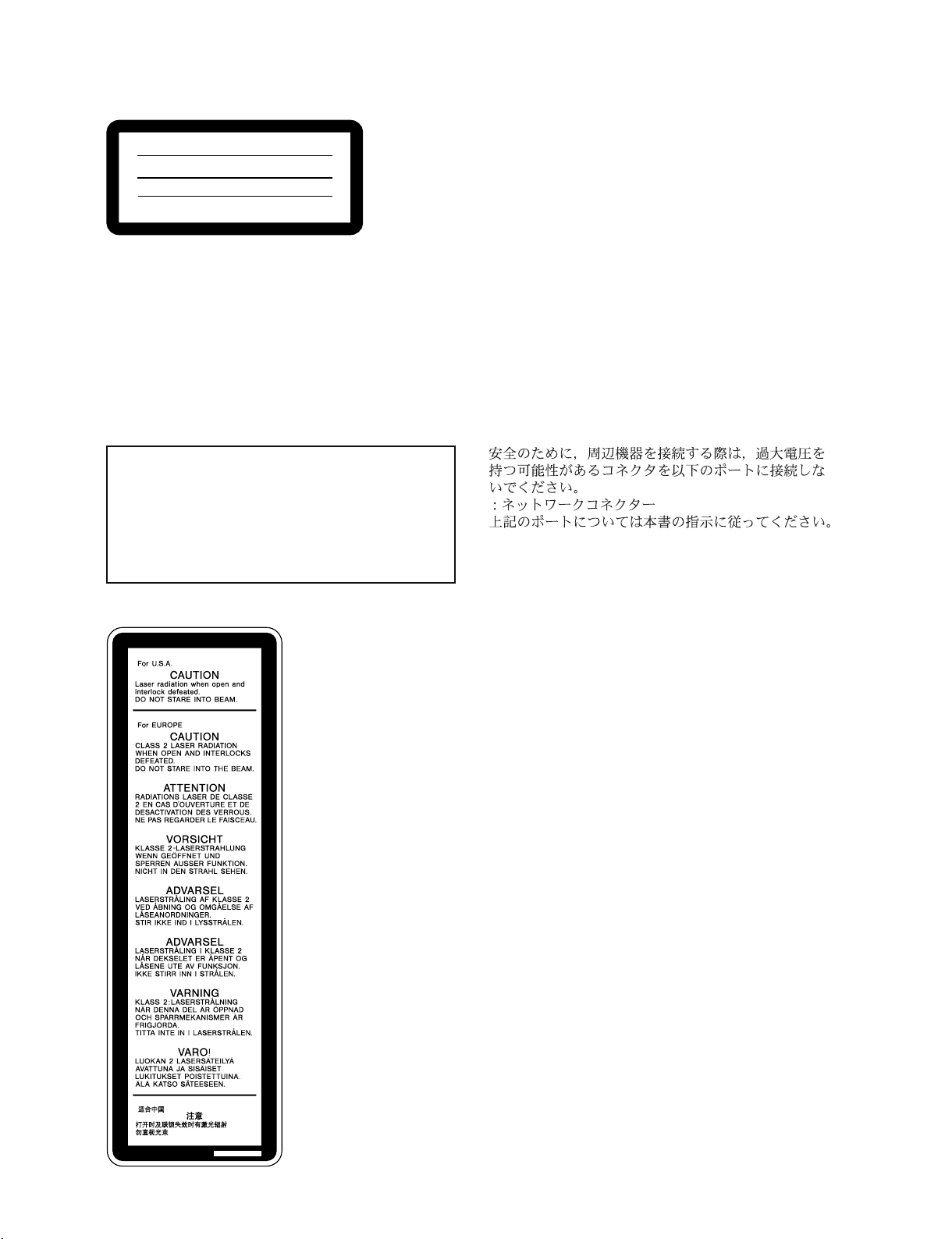
CLASS 1 LASER PRODUCT
LASER KLASSE 1 PRODUKT
LUOKAN 1 LASERLAITE
KLASS 1 LASER APPARAT
This Professional Disc Camcorder is classified
as a CLASS 1 LASER PRODUCT.
Laser Diode Properties
Wavelength: 400 to 410 nm
Emission duration: Continuous
Laser output power: 135 mW (max. of pulse peak),
65 mW (max. of CW)
Standard: IEC60825-1 (2001)
GEFAHR
Bei geöffnetem Laufwerk und beschädigter oder
deaktivierter Verriegelung tritt ein unsichtbarer
Laserstrahl aus. Direkter Kontakt mit dem
Laserstrahl ist unbedingt zu vermeiden.
This label is located
insidethe outside panel
of the unit.
CAUTION
The use of optical instruments with this product will
increase eye hazard.
Use of controls or adjustments or performance of
procedures other than those specified herein may result
in hazardous radiation exposure.
X-RAY RADIATION WARNING
Be sure that parts replacement in the high voltage block
and adjustments made to the high voltage circuits are
carried out precisely in accordance with the procedures
given in this manual.
For safety, do not connect the connector for peripheral
device wiring that might have excessive voltage to the
following port(s).
: Network connector
Follow the instructions for the above port(s).
2 (P)
PDW-700/V1 (E)
Page 5

Table of Contents
Manual Structure
Purpose of this manual ................................................................. 5
Related manuals ........................................................................... 5
1. Service Overview
1-1. Locations of Main Parts .................................................. 1-1
1-1-1. Locations of the Printed Wiring Boards ................ 1-1
1-1-2. Locations of Main Mechanical Parts ..................... 1-3
1-2. Circuit Description.......................................................... 1-4
1-2-1. Camera System ...................................................... 1-4
1-2-2. CCD Block ............................................................ 1-5
1-2-3. Video Signal System ............................................. 1-5
1-2-4. System Control ......................................................1-6
1-2-5. Digital Audio System .......................................... 1-12
1-2-6. Audio System ...................................................... 1-12
1-2-7. Audio DSP Operation Processing ....................... 1-14
1-2-8. Optical Drive System .......................................... 1-16
1-2-9. Power Supply Systems ........................................ 1-17
1-2-10. LCD System ........................................................ 1-18
1-2-11. Others .................................................................. 1-18
1-3. Matching Connectors .................................................... 1-20
1-4. Signal Inputs and Outputs ............................................. 1-20
1-5. On-Board Switch and LED Function ........................... 1-24
1-6. How to Take Out a Cartridge Manually ....................... 1-34
1-6-1. Taking Out a Cartridge at Power-off ................... 1-34
1-6-2. When You Cannot Take Out a Cartridge Even
If Pressing the EJECT Button at Power-on .........1-34
1-7. Removing/Installing ..................................................... 1-35
1-7-1. Removing Outside Panel .....................................1-35
1-7-2. Reinstalling Outside Panel .................................. 1-35
1-7-3. Inside Panel ......................................................... 1-35
1-7-4. Handle Assembly ................................................1-36
1-7-5. Front Panel .......................................................... 1-37
1-7-6. SW Guard Assembly ...........................................1-38
1-7-7. Shoulder Pad, Connector Cover .......................... 1-38
1-7-8. Connector Panel Assembly .................................1-39
1-7-9. Rear Panel Assembly .......................................... 1-40
1-7-10. Battery Connector ............................................... 1-40
1-8. Removing/Installing LCD Block .................................. 1-41
1-8-1. LCD Block .......................................................... 1-41
1-8-2. LCD Hinge .......................................................... 1-43
1-8-3. LCD Backlight and LCD Panel ........................... 1-44
1-9. Replacing the Flat Cables, Flexible Card
Wires/Boards ................................................................1-45
1-10. Service Tools/Measuring Equipment List .................... 1-46
1-10-1. Service Tools .......................................................1-46
1-10-2. Measuring Equipment ......................................... 1-47
1-11. Firmware/Software ....................................................... 1-48
1-11-1. EEPROM/FRAM List .........................................1-48
1-11-2. Firmware Update Using the USB Memory ......... 1-49
1-11-3. Software Option Registration Method
by Using USB Memory .......................................1-51
1-12. Other Overview ............................................................ 1-52
1-12-1. Notes on Handling Optical Block Assembly ...... 1-52
1-12-2. Standard Torque for Screws ................................1-53
1-12-3. Stop Washer ........................................................ 1-53
1-12-4. Description of CCD Block Number ....................1-54
1-12-5. Memory Backup Battery ..................................... 1-54
1-12-6. IC Link Replacement ..........................................1-54
1-12-7. Circuit Protection Element ..................................1-54
1-12-8. Precautions for Use of Condensation Sensor ...... 1-55
1-12-9. Precautions for the Battery Connector ................ 1-55
1-12-10. Notes on Repair Parts ..........................................1-55
1-12-11. Unleaded Solder .................................................. 1-55
2. XDCAM Web Site
2-1. XDCAM Web Site Overview ......................................... 2-1
2-2. Status Menu .................................................................... 2-3
2-2-1. Device Information ............................................... 2-3
2-2-2. Hours Meter ........................................................... 2-4
2-2-3. Software Version ................................................... 2-5
2-3. Disc Menu....................................................................... 2-7
2-3-1. Disc Properties ...................................................... 2-7
2-3-2. Thumbnails ............................................................2-7
2-4. Maintenance Menu ......................................................... 2-8
2-4-1. Software Update ....................................................2-8
2-4-2. Account ............................................................... 2-13
2-4-3. Network ...............................................................2-14
2-4-4. License Registration ............................................2-15
PDW-700/V1 (E)
1
Page 6

3. Error Messages
3-1. Error Messages Overview............................................... 3-1
3-2. Error Code List ............................................................... 3-2
3-2-1. Main Code and Sub Code ...................................... 3-2
3-2-2. Error 0X ................................................................. 3-3
3-2-3. Error 20 .................................................................3-4
3-2-4. Error 3X ................................................................. 3-5
3-2-5. Error 5X ................................................................. 3-5
3-2-6. Error 6X ................................................................. 3-5
3-2-7. Error 91 .................................................................3-6
3-2-8. Error 92 .................................................................3-7
3-2-9. Error 95 .................................................................3-7
4. Setup Menu
4-10-19. SKEW .................................................................. 4-97
4-10-20. SERVO_2 ............................................................ 4-97
4-10-21. ACCELERATION OFFSET ...............................4-98
4-10-22. ERROR LOGGER .............................................. 4-99
4-10-23. VERSION .......................................................... 4-100
4-10-24. SERIAL NO ...................................................... 4-100
4-10-25. CLEAR MEDIA LOG ......................................4-100
4-10-26. UPLOAD TO EEPROM ................................... 4-100
4-11. AUDIO A/D Error Correction .................................... 4-101
4-12. AUDIO D/A Error Correction .................................... 4-102
4-13. AUDIO LEVEL Volume Compensation ....................4-102
4-14. Adjusting Battery End Detection Voltage .................. 4-103
4-15. SERVICE SUPPORT Menu .......................................4-104
4-16. Setup Menu List .......................................................... 4-105
4-1. Setup Menus ................................................................... 4-1
4-1-1. Basic Operations of Setup Menus ......................... 4-1
4-1-2. How to Display the SERVICE Menu .................... 4-1
4-2. TOP Menu ...................................................................... 4-2
4-3. USER Menu .................................................................... 4-3
4-4. OPERATION Menu ....................................................... 4-4
4-5. PAINT Menu ................................................................ 4-27
4-6. MAINTENANCE Menu ............................................... 4-38
4-7. FILE Menu.................................................................... 4-56
4-8. DIAGNOSIS Menu ...................................................... 4-65
4-9. SERVICE Menu ........................................................... 4-69
4-10. Drive Maintenance ........................................................ 4-85
4-10-1. Basic Operation on Drive Maintenance
Menus .................................................................. 4-85
4-10-2. TEMPERATURE SENSOR ............................... 4-85
4-10-3. DEW SENSOR ................................................... 4-86
4-10-4. FAN MOTOR ..................................................... 4-86
4-10-5. ACCELERATION SENSOR ..............................4-87
4-10-6. LOADER ............................................................. 4-88
4-10-7. SLIDER-AUTO TEST ........................................4-91
4-10-8. IN-LIM TEST ..................................................... 4-91
4-10-9. OUT-LIM TEST ................................................. 4-92
4-10-10. SPINDLE MOTOR-AUTO TEST ...................... 4-92
4-10-11. FOCUS ACTUATOR ......................................... 4-93
4-10-12. TRACKING ACTUATOR ................................. 4-94
4-10-13. SA ACTUATOR ................................................. 4-94
4-10-14. LASER ................................................................ 4-95
4-10-15. ND FILTER ......................................................... 4-95
4-10-16. SKEW .................................................................. 4-96
4-10-17. LENS CLEANING ............................................. 4-97
4-10-18. SERVO_1 ............................................................4-97
5. File System
5-1. Structure of File System ................................................. 5-1
5-2. Data Structure .................................................................5-2
5-3. Operating the Files and the Data Flow ........................... 5-3
5-3-1. USER FILE ........................................................... 5-3
5-3-2. ALL FILE .............................................................. 5-5
5-3-3. REFERENCE FILE ............................................... 5-7
5-3-4. Other FILE (SCENE FILE and LENS FILE) ....... 5-9
5-3-5. SERVICE FILE ...................................................5-10
5-3-6. Other RESET ....................................................... 5-11
5-4. Special Items to Save .................................................... 5-12
5-4-1. White Gain .......................................................... 5-12
5-4-2. Master Gain .........................................................5-13
5-4-3. Shutter .................................................................5-13
6. Periodic Maintenance and Inspection
6-1. Periodic Check/Replacement Parts List.......................... 6-1
6-2. Cleaning .......................................................................... 6-2
6-2-1. General Information for the Use of Cleaning
Cloth ......................................................................6-2
6-2-2. Cleaning Loader Assembly ................................... 6-2
6-2-3. Cleaning Spindle Motor ........................................ 6-3
6-2-4. Cleaning Pickup Lens ............................................ 6-3
6-3. Cares after Using under Special Environment................ 6-4
6-4. Digital Hours Meter ........................................................6-5
6-4-1. Display Method and Reset Methods ..................... 6-5
6-5. Recommended Replacement Parts ................................. 6-6
6-6. Precautions for the Battery Connector ............................ 6-8
6-7. Precaution on Hanging Bracket of Handle .....................6-8
2
PDW-700/V1 (E)
Page 7

7. Replacement of Main Parts
7-1. Optical Drive Assembly ................................................. 7-1
7-1-1. Removing/Reinstalling Loader Assembly ............7-1
7-1-2. Removing/Reinstalling Drive Sub Assembly .......7-5
7-1-3. Replacing Cleaner Assembly ................................ 7-7
7-1-4. Replacing Loading Motor Assembly .................... 7-8
7-1-5. Replacing Optical Block Assembly ......................7-9
7-1-6. Replacing No.2/No.3 Gear Assemblies ............... 7-12
7-1-7. Replacing Seek Motor Assembly ........................7-14
7-1-8. Replacing Spindle Motor .................................... 7-15
7-1-9. Removing/Reinstalling Lock Release
Assembly .............................................................7-16
7-1-10. Removing/Reinstalling LD Motor ...................... 7-17
7-2. Removing/Reinstalling Mounted Circuit Board of the
Optical Drive ................................................................ 7-18
7-2-1. SE-709 Board ..................................................... 7-18
7-2-2. SE-857 Board ..................................................... 7-19
7-2-3. SE-858 Board ..................................................... 7-21
7-3. Replacing Fan Motor (Drive) ....................................... 7-23
7-4. Replacing Fan Motor (Rear) .........................................7-24
7-5. Removing/Reinstalling CCD Unit ................................ 7-25
7-5-1. Removing CCD Unit ...........................................7-25
7-5-2. Reinstalling CCD Unit ........................................ 7-26
7-6. Service Action After Replacing the CCD Unit............. 7-27
7-7. Removing/Installing Boards .........................................7-28
7-7-1. CN-2947 Board and TG-260 Board .................... 7-28
7-7-2. AT-177 Board and DCP-44 Board ......................7-28
7-7-3. DVP-45 Board and SY-355 Board ......................7-29
7-7-4. ENC-118 Board, HP-148 Board and
SW-1391 Board ...................................................7-29
7-7-5. FP-157 Board ...................................................... 7-30
7-7-6. CN-2946 Board and CN-3026 Board ..................7-31
7-7-7. KY-623 Board ..................................................... 7-32
7-7-8. CN-3025 Board and SW-1425 Board ................. 7-32
7-7-9. CN-3001 Board ................................................... 7-33
7-7-10. IO-235 Board ....................................................... 7-33
7-7-11. CI-37 Board .........................................................7-33
7-7-12. PS-731 Board ...................................................... 7-34
7-7-13. AXM-38 Board, CN-2948 Board,
SW-1352 Board and RM-216 Board ................... 7-34
7-7-14. MS-86 Board ....................................................... 7-34
7-7-15. CNB-25 Board and PS-708 Board ...................... 7-35
7-7-16. CN-3005 Board and SW-1426 Board ................. 7-35
7-7-17. DR-606 Board ..................................................... 7-36
7-7-18. RE-246 Board ...................................................... 7-37
7-7-19. RX-101 Board ..................................................... 7-37
7-7-20. MB-1111 Board ................................................... 7-38
7-8. Service Action After Replacing or Repairing
the Board ....................................................................... 7-39
7-8-1. Optical Block Assembly ...................................... 7-39
7-8-2. AT-177 Board .....................................................7-39
7-8-3. CN-3005 Board ................................................... 7-39
7-8-4. DCP-44 Board .....................................................7-39
7-8-5. SY-355 Board ...................................................... 7-40
7-8-6. FP-157 Board ...................................................... 7-40
7-8-7. DR-606 Board ..................................................... 7-40
7-8-8. SE-857 Board ...................................................... 7-40
8. Optical Drive Alignment
8-1. Optical Drive Alignment Overview................................ 8-1
8-1-1. Precautions ............................................................ 8-1
8-1-2. Fixtures .................................................................. 8-1
8-1-3. Preparations Before Adjustment ........................... 8-1
8-2. Procedures After Replacing the Optical Block
Assembly and the Board .................................................8-1
8-2-1. Adjustment After Replacing the Optical
Block Assembly .................................................... 8-1
8-2-2. Adjustment After Replacing the DR-606
Board ..................................................................... 8-1
8-2-3. Adjustment After Replacing the SE-857 Board ....8-1
8-3. Servo1 Automatic Adjustment ....................................... 8-2
8-4. Skew Adjustment ............................................................ 8-3
8-4-1. Tangential Skew Adjustment ................................ 8-3
8-4-2. Radial Skew Adjustment .......................................8-5
8-5. Servo2 Automatic Adjustment ....................................... 8-6
8-6. Clearing Media Log ........................................................ 8-6
8-7. After Adjustment ............................................................ 8-6
PDW-700/V1 (E)
3
Page 8

9. Electrical Alignment
9-1. Preparation ...................................................................... 9-1
9-1-1. Fixtures and Equipment ........................................9-1
9-1-2. Connection ............................................................9-1
9-1-3. Switch Setting before Adjustment ......................... 9-2
9-1-4. Notes on Adjustment .............................................9-2
9-1-5. Gray-Scale Chart and its Maintenance ..................9-3
9-2. Adjustment ...................................................................... 9-4
9-2-1. Confirming VCO CONT Frequency .....................9-4
9-2-2. Modulator Balance Adjustment ............................9-4
9-2-3. VA Gain Adjustment ............................................. 9-5
9-2-4. Black Shading Adjustment ....................................9-6
9-2-5. White Shading Adjustment ................................... 9-7
9-2-6. Black Set Adjustment ............................................9-8
9-2-7. Flare Adjustment ...................................................9-9
9-2-8. Auto Iris Adjustment ...........................................9-10
9-2-9. RPN Adjustment ................................................. 9-11
9-2-10. S/H DC Adjustment ............................................ 9-12
9-2-11. RPN Correction Procedure ..................................9-13
4
PDW-700/V1 (E)
Page 9

Purpose of this manual
Related manuals
Manual Structure
There are volume 1 and volume 2 in the Maintenance manual of PDW-700.
The maintenance manuals (volume 1, 2) are intended for use by trained system and
service engineers, and provides the information of maintenance and detailed service.
The following manuals are available in this model.
If this manual is required, please contact your local Sony Sales Office/Service
Center.
..
. Operation Manual (Supplied with the unit)
..
This manual is necessary for application and operation (and installation) of this
unit.
..
. Maintenance Manual
..
Volume 1: Describes about maintenance information, parts replacement, and
guideline for adjustment.
Part number: 9-968-417-03
Volume 2: Describes about block diagrams, schematic diagrams, board layouts
and detailed parts list required for parts-level service.
Part number: 9-968-435-03
..
. “Semiconductor Pin Assignments” CD-ROM
..
This “Semiconductor Pin Assignments” CD-ROM allows you to search for
semiconductors used in Broadcast and Professional equipment.
This manual contains a complete list of semiconductors and their ID Nos., and
thus should be used together with the CD-ROM.
Part number: 9-968-546-06
PDW-700/V1 (E)
5
Page 10

Page 11
Section 1
Service Overview
1-1. Locations of Main Parts
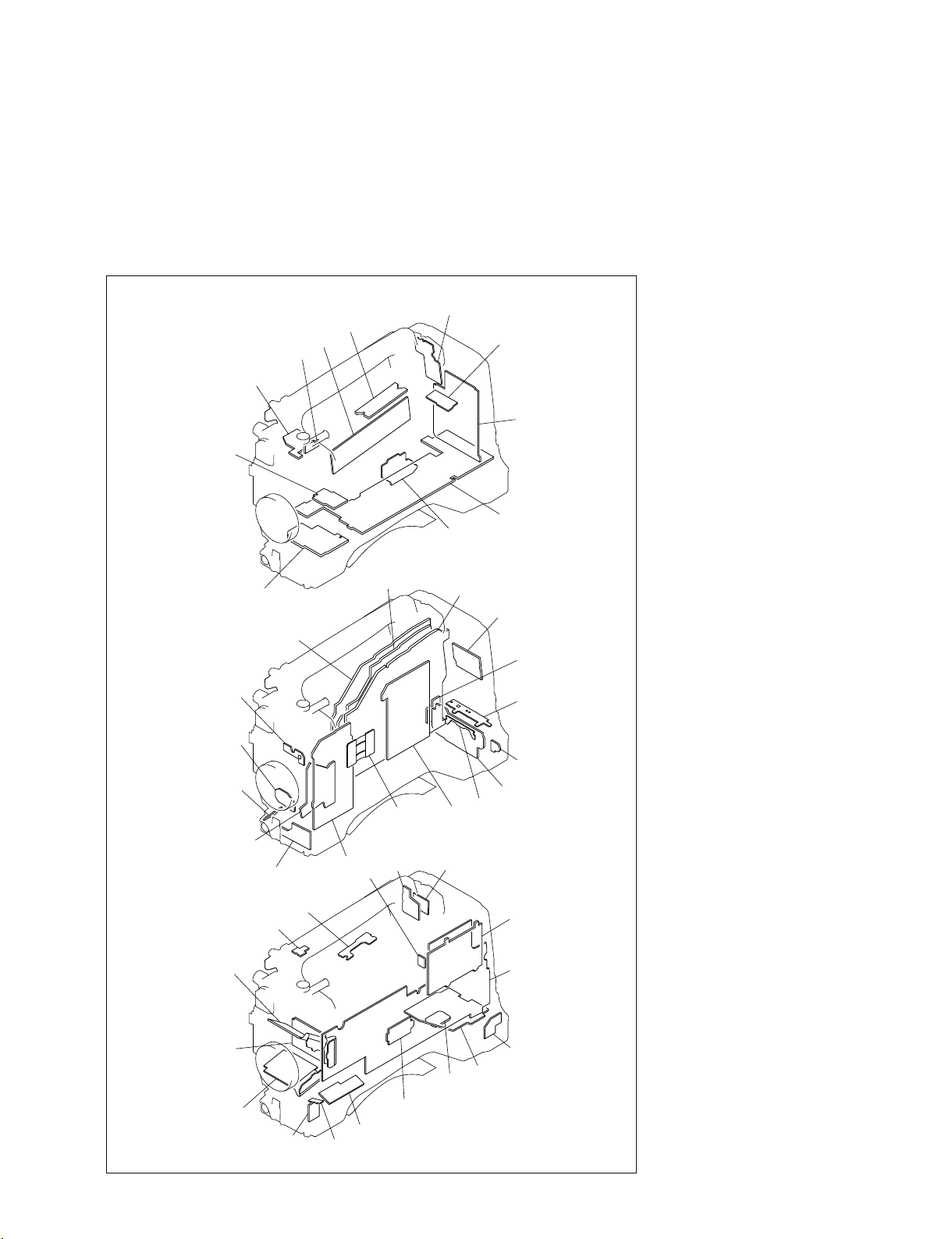
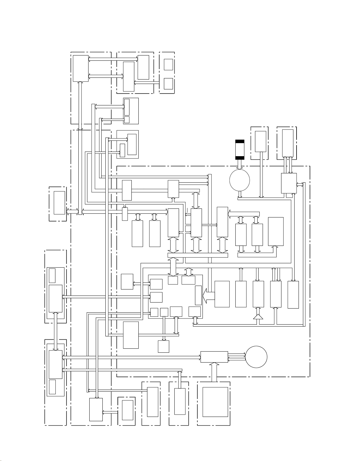
1-1-1. Locations of the Printed Wiring Boards
Main unit
@\
#/
@.
#'
7
9
@,
!;
8
@'
$=
#,
@/
!'
$[
$/
!\
!,
$\
@[
$-
![
$]
5
@]
#[
#;
1 AT-177
2 AXM-38
3 CI-37
4 CN-2946
5 CN-2947
$- SW-1391
$= SW-1425
$[ SW-1426
$] SY-355
$\ TG-260
6 CN-2948
#]
7 CN-3001
8 CN-3005
9 CN-3025
0 CN-3026
!- CNB-25
@=
@;
!= DCP-44
![ DET-45
!] DET-47
!=
3
!\ DR-606
!; DR-617
!' DVP-45
!, ENC-118
6
!. FP-157
@/ HP-148
#.
@- HP-149
@= IO-235
@[ KY-623
1
!]
#\
2
@] LED-444
@\ MA-162
@; MB-1111
@' MS-86
!/4
@, PA-342/342A
@. PA-343/343A
#/ PA-344
#-
#- PD-118
#= PS-708
!.
#[ PS-731
#] RE-246
#\ RM-216
#; RX-101
#' SE-924
#, SW-1249
#. SW-1352
#=
@-
!-
$/ SW-1385
PDW-700/V1 (E)
1-1
Page 12
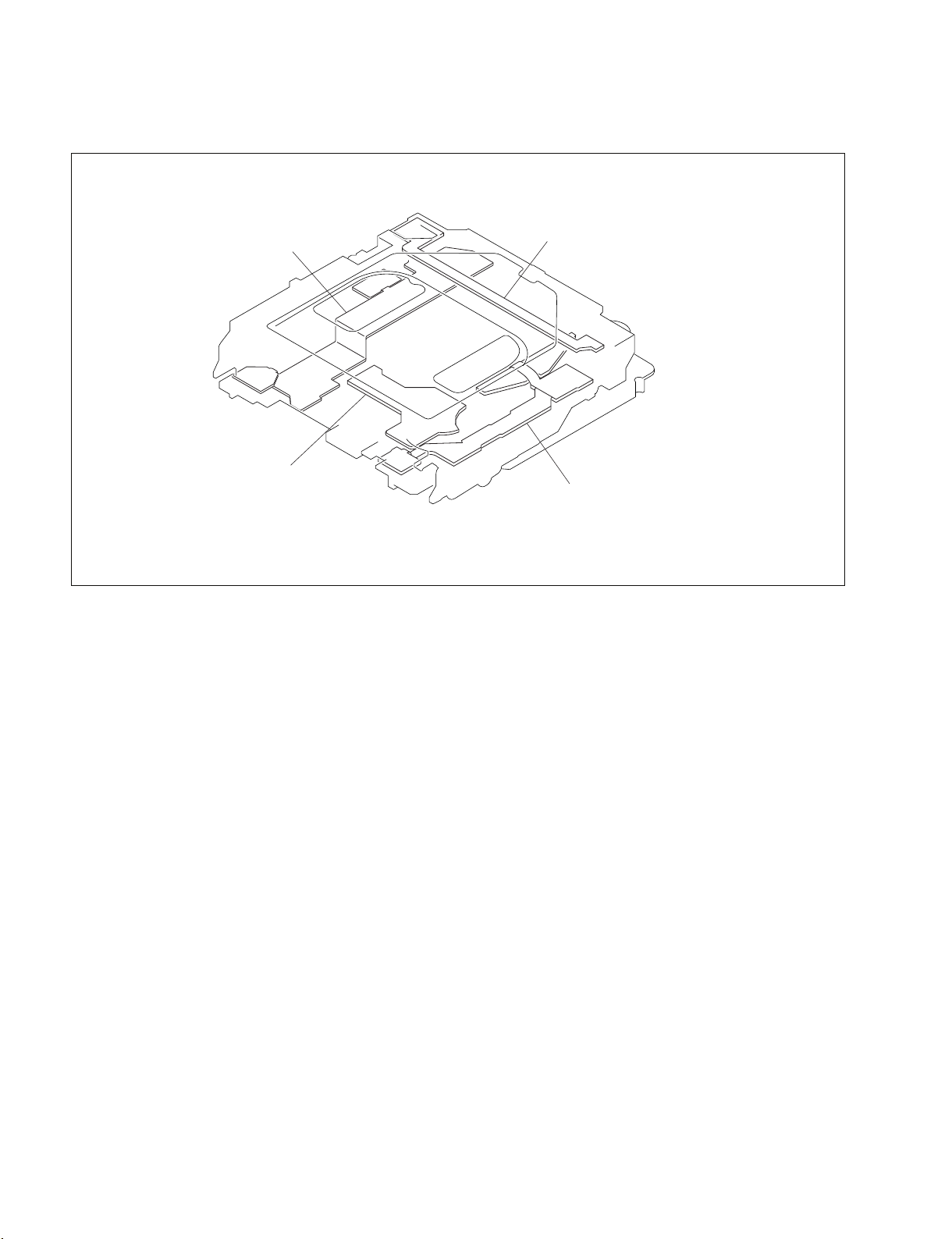
Optical drive
1 SE-709
2 SE-857
3 SE-858
4 SW-1125G
1
2
4
3
1-2
PDW-700/V1 (E)
Page 13
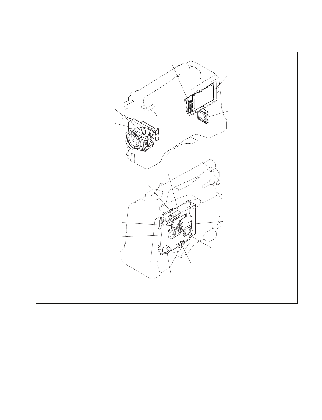
1-1-2. Locations of Main Mechanical Parts
3
4
2
1

1-2. Circuit Description
1-2-1. Camera System
AT-177 board
The AT-177 board is the microprocessor board that
controls the camera block.
DCP-44 board
The DCP-44 board consists of the block for A/D conversion
of the analog RGB signal from the PA-342/PA-342A/PA343/PA-343A/PA-344 board via the feedback clamp circuit,
the cam-era DSP block that performs the signal processing,
the dri-ver block that sends the analog signal that is D/A convert-ed to the outputs, and the I/F block to the AT-177 board.
1. Microprocessor peripherals
The CPU (IC209) uses SH2A (R5S7206), and the clock provides 32 MHz from an external source that is six multiplication in the CPU so that the clock runs on 192 MHz. The memory is composed of 64 MBit flash memory (IC302, IC303), 16
MBit SRAM (IC3056), and 1 MBit FRAM (IC308).
2. A/D input of the CPU
The A/D port equipped to the CPU is connected to the
following signal lines and monitored: CC position, ND
position, temperature, IRIS position of a camera lens,
ZOOM position, and mic volume level.
3. Internal communication
The serial communication includes intercommunication
with the BleConSh IC on the DCP-44 board, the writing
controls to the character generator IC, and
intercommunication with the disc.
The parallel communication is equipped with the 8-bit data
line, the total 11-bit address line (A0-A7, A14-A16),
control line clock, XRD, XWR, OE, DIR, CS, and
(QWERTY, ZXCV, TG).
In addition, the intercommunication is performed with
EEPROM on the DCP-44 board, the DAC and I/O port IC
for the video signal, and the I/O port IC on the FP-157
board with the I2C line that is installed directly to the CPU.
4. Memory stick circuit
The memory stick controller IC (IC610) is driven at 16
MHz, and the two-way communication and the clock
signal are directly connected from the connector (CN602)
to the memory stick connector of the MS-86 board via the
coaxial harness. This is compatible with the Memory Stick
PRO/DUO.
5. External communication
The 2 channel serial communication driver CXD9093R
(IC411) is equipped and performs external communication
with the remote control unit RM-B150/B750.
6. ROM jig connector (CN601)
The connector CN101 that can be connected to the jig for
writing the boot program (MS-86 board) is included.
1-4
After passing through the pre-filter (FL300 to FL302), the
analog RGB signal input from the PA-342/PA-342A/PA343/PA-343A/PA-344 board is converted to 74 MHz rate
14-bit digital RGB sign-al by the A/D converter (IC107 to
IC109), then input into the camera processor IC (IC600).
The camera signal processor IC (IC600) detects the
average value and the peak value of the camera video
signals that are required for the AUTO operations of the
camera such as AUTO black balance, AUTO white
balance, and AUTO iris control. The detected average
value and peak value are sent to the AT-microprocessor on
the AT-177 board. In addition to the above operations, the
25/30 PsF conversion function and the 1080 to 720
conversion function are realized by using the DDR
SDRAM (IC700 to 704).
After passing through white balance, white shading, and
flare correction, the camera main video signal performs the
Digital GAIN UP, then performs the Digital Noise
Reduction. Then, the matrix signal and the detail signal are
added to perform pedestal control, gamma correction, knee
correction, and white clip processing. After passing
through the selector circuit with which either the camera
main video signal or the color bar signal can be selected,
the selected signal is output from IC (IC600) to IC800.
The digital VBS signal and the digital Y signal for VF
supplied from the camera signal processor IC (IC800) are
converted into the analog VBS signal and analog VF signal
by the D/A converter* (IC1513, IC1524, IC1525). After
passing through the circuit with which either the camera
analog VBS signal or the VF Y can be selected, the
selected signal is output to the TEST OUT connector.
After passing through the circuit with which either the
GENLOCK IN connector input or the video signal can be
selected, the selected signal is output to the VF connector.
In addition, the sync separation circuit and the PLL circuit
to synchronize with the external input video of the GENLOCK IN connector are included.
The detected average value of the video signal detected in
the camera signal processor IC (IC600) and peak value are
loaded to the AT-microprocessor on the AT-177 board
through the 8-bit data bus.
PDW-700/V1 (E)
Page 15

At the same time, various control signals are controlled by
the AT-177 board via I/O Expander (IC3, IC4, IC67).
All volumes are controlled electronically, and the level
adjustment is adjusted from the menu.
are generated by IC8 and are sent to the DR-617 board.
These pulses are generated from the 74 MHz clock in
synchronization with the HD VD signal input from the
DCP-44 board. In addition, the TG-260 board has an
interface circuit with the optical filter.
The main functions of IC800 are the down-conversion HD
to SD, the conversion 720 to 1080 for VF output, and the
VF DETAIL generation processing digital ECN
processing.
The camera main signal of the SD system is output to IC1000.
After performing the multiplex and parallel-serial
conversion on the character signal, audio signal, and the
ancillary signal in IC1000, the HD signal and SD signal
output from IC800 pass through IC (IC1112, IC1113) and
are output to SDI1 and SDI2 connectors as the HD-SDI
and SD-SDI signals. After another system performs scaling
in IC1000 through the SDRAM (IC1309), the HD signal
output from IC800 passes through the D/A converter
(IC1518) and the video signal is sent to the LCD display.
The HD signal output from IC600 is sent to the recording
system (DVP-45 board) through multiple character signals
in IC1000. After the signal from the RX-105 board on the
SDI input option and the SDI signal from the 50-pin I/F are
selected internally in IC1000, the signals are separated into
the video signal, audio signal, and the ancillary signal, then
sent to the recording system (DVP-45 board).
* :The main functions of IC800 are the down-conversion HD to SD, the
conversion 720 to 1080 for VF output, and the VF DETAIL generation
processing digital ECN processing. The camera main output of the SD
system is output to IC1000.
1-2-2. CCD Block
PA-342/PA-342A/PA-343/PA-343A/PA-344 board
The CCD drive pulses that are supplied from the TG-260
board are amplified so that these pulses can drive the CCD
imagers directly (IC2: H Driver). On the other hand, the
CCD output signals are amplified approximately two times
and input to IC10. The video signal is drawn by the co-related dual sampling inside IC10 and GAIN UP of 0 to 12
dB is performed by the internal GAIN AMP. In addition,
the differences in the CCD sensitivity are adjusted by
adjusting GAIN. In addition to the above operations, the
temperature that is detected by the temperature sensor
(IC4) is converted to the voltage data and is sent to the AT177 board via the DCP-44 board.
TG-260 board
The pulses that drive the CCD imagers and the pulses that
are used for sample-and-hold of the CCD output signals
DR-617 board
The CCD drive pulses input from the TG-260 board and
the sample-and-hold pulse are latched and output to the
PA-342/PA-342A/PA-343/PA-343A/PA-344 boards. In
addition, the DR-617 board has the V driver of CCD.
The CCD V sub voltage and CCD sensitivity adjustment
data are recorded in the EEPROM (IC20).
1-2-3. Video Signal System
DVP-45 board
1. Baseband/Video signal processing system
<Recording system>
The component parallel digital video signal supplied from
the video circuit of the DCP-44 board is input to LVIS
(IC400) of the DVP-45 board.
Signal pre-processing such as the filtering and scaling is
performed in this system.
<Playback system>
The playback digital video data is loaded from LVIS
(IC400) and sent to the DCP-44 board via the MB board as
the component parallel digital video signal.
The component parallel digital video signal sent to the
DCP-44 board is distributed to each path of HD/SD-SDI,
VF, COLOR-LCD, and down-conversion and encoding to
the composite video signal are performed according to the
setting.
2. Video compression signal processing system
<Recording system>
The recording digital video signal that has undergone
signal processing on the DVP-45 board is sent to MPEG2VIDEO Codec (TORINO: IC1000, 1200, 1400) and
compressed to the MPEG-2 VIDEO format.
The compressed digital video data is sent to PIER G4
(IC1900) and written to PIER_SDRAM (IC1901 to IC1904).
The recording digital video signal is encoded to MPEG4VIDEO format in LVIS (IC400) at the same time and
generated as the Proxy video data.
The generated Proxy video data is sent to PIER G4
(IC1900) and written to PIER_SDRAM (IC1901 to IC1904).
PDW-700/V1 (E)
1-5
Page 16

The recording digital data via i.LINK/network is sent to
PIER G4 (IC1900) via the PCI bus and written to
PIER_SDRAM (IC1901 to IC1904).
While recording on a disc, the data in PIER_SDRAM
(IC1901 to IC1904) is sent to the DR-606 board via the
ATA interface.
<Playback system>
The playback video data and the Proxy video data are sent
to PIER G4 (IC1900) via the ATA interface and written to
PIER_SDRAM (IC1901 to IC1904).
The playback digital video data in PIER_SDRAM (IC1901
to IC1904) is sent to the MPEG2-VIDEO Codec (TORINO: IC1200, IC1400). Decode processing is performed
and then the data is sent to LVIS (IC400).
The playback Proxy video data in PIER_SDRAM (IC1901
to IC1904) is sent from PIER G4 (IC1900) to LVIS
(IC400) and decode processing is performed.
The Proxy video data is used as the video signal during the
search.
The playback video data in PIER_SDRAM (IC1901 to
IC1904) is provided to i.LINK/network via the PCI bus as
the MXF file data.
3. Sync signal system
Whether the status is on record or on playback, 74/27 MHz
clock, HD-F, HD-V, HD-H, HD-PB-F, SD-F, SD-V, and
SD-H that are always input from the DCP-44 board are the
reference signal.
Based on these reference clocks, the video sync timings
and system timings are generated.
1-2-4. System Control
SY-355 board
1. Disc record/playback system control
The following functions are realized using the RISC
microprocessor (hereinafter refer to as CPU: IC 200) as the
CPU for the system control on the SY-355 board.
<PCI bus interface>
CPU is connected to PIER G4 (IC1900/DVP-45 board)/
FAM controller on the DVP-45 board and PCI-PCI Bridge
(IC900) via the PCI bus interface to receive and send data
with one another and perform control.
The PCI bus interface communicates with the following
devices by relaying through PIER G4 (IC1900/DVP-45
board).
. CAVA (IC200/DVP-45 board)
. MPEG2-VIDEO CODEC (IC1000, 1200, 1400/DVP-45
board)
. AUDIO REC/PB DSP (IC800, 801/DVP-45 board)/
AUDIO Low Resolution DSP (IC900/DVP-45 board)
. LVIS (IC400/DVP-45 board)
. Optical Drive (DR-606 board)
. AT microprocessor (AT-177 board)
. FP microprocessor (FP-157 board)
. Character generator (IC503/DCP-44 board)
. LTC generator/reader (PIER G4 (IC1900) built-in)
The PCI bus interface is connected to the Linux system on
the SY-355 board via the PCI-PCI Bridge (IC900/SY-355
board) and receives and sends data to the controllers.
<Memory controller>
. SDRAM (SY-355 board: IC201 to 204) control (32 bit x
64M word)
. Flash memory (IC505, IC506/SY-355 board) control (32
bit x 16 M word)
<Serial interface>
. EEPROM control saving the setting data
<External control bus (CPU LOCAL bus)>
. IN port/OUT port control
RESET signal output on each device, loading the switch
setting, and similar signals
.
CAVA/PIER G4/FAM/BRIDGE each FPGA
configuration
. FRAM (IC507/SY-355 board) control
2. Application device control system (Linux)
This is the system that uses RISC microprocessor
(hereinafter refer to as CPU: IC1300) on the SY-355 board
to control the device for the application. Linux is used as
the OS.
CPU and peripheral circuit configuration is almost same as
that of the system control.
<PCI bus interface>
The CPU exchanges data with the USB controller
(IC1500) via the PCI bus interface. In addition, the CPU
exchanges the data with the CPU of the system control via
the PCI-PCI Bridge (IC500/SY-355 board) on the same
bus.
<PCI BRIDGE (IC900)>
The functions of PCI BRIDGE are data relay of the PCI
bus and the I/F function to the OSD display controller on
the LVIS (IC400/DVP-45 board).
1-6
PDW-700/V1 (E)
Page 17

<USB HOST Controller (IC1500)>
USB HOST Controller exchanged data with the USB
devices such as the flash memory using the interface
compatible with the USB 2.0.
<Ether interface>
Ether interface controls the Ether PHY (IC1/CN-2946
board) and connects to the network via it.
FP-157 board
12. FP_CPU backup circuit
13. Backup lithium battery voltage measurement circuit
14. Independent operation of FP_CPU
15. REAR input control
16. REAR XLR automatic insertion detection circuit
control (DET-47 board and sensor holder)
17. Color LCD monitor drive control and switching/
rotation detection circuit
18. Nonvolatile memory control
19. Monochrome LCD display circuit with back light
The FP-157 board has the FP_CPU (IC921) as the submicroprocessor and the hardware consists of the synchronous and asynchronous serial communication, I2C communication bus, and the 8-bit bus. The main function is
controlling the audio system.
Main functions
. Synchronous serial communication
The functions of synchronous serial communication are
the color LCD monitor setting, monochrome LCD
display, audio D/A setting, analog wireless communication, and the ITORON communication.
. Asynchronous serial communication
Digital wireless communication.
. I2C bus
The rear connector, detection such as PLAY/STOP key,
Info_BATTERY communication, Real Time Clock
communication, Serial EEPROM (Memory) communication, and I/O control communication make up the 3channel I2C bus.
. 8-bit bus
The 8-bit bus controls the serial communication bus
(SDA,SCL) of the 3-channel I2C bus controller (Parallel
bus to I2C_bus Controller).
. CPU I/O
The CPU I/O loads the A/D and controls the I/O port
terminal.
Main blocks
1. Audio mode control
2. AUDIO level indication
3. STOP/PLAY keys control
4. CTL/TC/UBIT control
5. Real Time Clock control
6. WARNING_LED control and alarm tone control
7. Wireless receiver (optional equipment) control
8. Software download function
9. Power supply voltage measuring circuit
10. Info-Battery communication circuit
11. POWER OFF soft control circuit
Description of each block
1. Audio mode control
Audio control is performed by receiving the audio mode
information and the menu setup information from the
ITORON (CPU) on the SY-355 board.
The switch information of the three positions is connected
to the AD terminal of the CPU and processed as the AD
signal of the three-valued data.
The audio is switched in the I2C bus PCA-9555 (I/O port:
IC923, 924).
2. AUDIO level indication
The digital signal applied on the DSP is converted to 16
bits and set in the register in DSP.
ITRON (CPU) reads and displays it on the color LCD
monitor. The peak hold time is approx. 1400 ms.
3. STOP/PLAY keys control
Each switch on the KY-623 board is connected to PCA9555 for I2C bus to read the ON/OFF information of the
switch and turn on the LED. The switch information is
transferred to ITORON (CPU).
At POWER-ON, the LED of EJECT, F REV, PLAY, F
FWD are turned on, initialized, and turned off.
4. CTL/TC/UBIT control
The switch information of the three positions is connected
to the AD terminal of the CPU and processed as the AD
signal of the three-valued data.
The ON/OFF information of the switches are transferred to
the ITRON (CPU) and displayed on the color LCD
monitor.
5. Real Time Clock control
The Real Time Clock IC (IC908:RX-8025NB) uses
nonadjustable clock for the I2C bus. The accuracy is ± 15
seconds per month. When the power is turned on, the
FP_CPU reads data and send it to ITRON (CPU)
The ITRON (CPU) sends the time data to the Camera CPU
PDW-700/V1 (E)
1-7
Page 18
of the AT-177 board. The viewfinder uses the time data for
displaying the time. The data for year, month, day, and
time of the clock can be changed using the menu.
The settings for year, month, day, and time are sent to the
FP_CPU and the year, month, day, and time are written to
the Real Time Clock IC.
6. WARNING_LED control and alarm tone control
The WARNING information is supplied from the ITRON
(CPU) that is used to turn on and off the WARNING LED
on the FP-157 board.
The 1 KHz square wave generated from the PWM generator circuit inside the FP_CPU alarm tone is used as the
alarm tone.
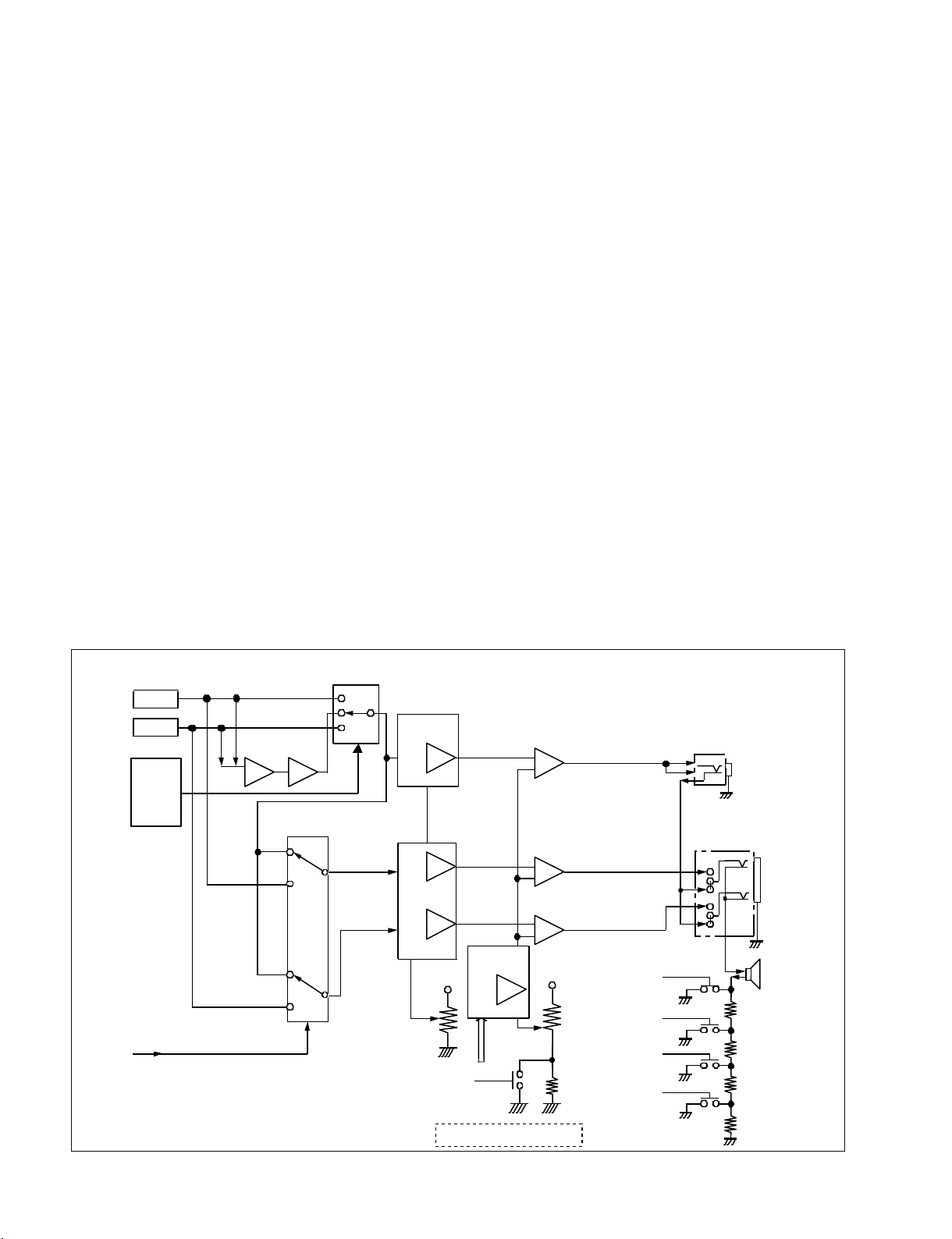
7. Wireless Receiver Control (Optional function)
This communication circuit can control both analog and
digital wireless receivers.
Analog wireless receivers use the conventional method of
synchronous serial communication (200 Bps).
(Interval time: 80 ms)
Digital wireless receivers use 38 KBps asynchronous serial
communication to handle large amounts of communication
data.
CH1&2
or
CH3&4
CH-1/3
CH-2/4
IC750
FP-CPU
(CH-1/3,
MIX,
CH-2/4)
FP-CPU(Head Phone Out:Streo/Mono)
MIX INV
Mono
CH-1/3
Streo
Mono
CH-2/4
Streo
CH-1/3
MIX
CH-2/4
IC704
TC74HC4052
IC705
TC74HC4052
SW
MONITOR-VR
FP_CPU (MIN ALARM VOL)
IC706
NJM-2172
VCA
+InA
OutA
_InA
Cont
OutB
+InB
_InB
VCA
OutA
+InA
_InA
Cont
RV700
ALARM SIGNAL(FP_CPU)
Audio Monitor Block
With a built-in wireless receiver, when FP_CPU is in the
POWER-ON state, the receiver type is determined and
information such as the transmission RF sensitivity is loaded. This data is transmitted to Camera CPU via ITRON
(CPU) and can be viewed on the viewfinder.
8. Software download function
FP_CPU has internal flash memory so the software can be
overwritten. Load the software in the memory stick into
the camera microcomputer and transmit the data through
ITRON (CPU) in the SY-335 board to the FP_CPU where
it is written.
9. Power voltage measurement circuit (batteries other
than the info battery)
Power voltage measurement circuit (IC839) outputs two
types of DC voltage from DA output of the FP_CPU and
switches voltage in the IC839 6-pin to switch between a
measurement range of +9 V to +14 V and +12 V to +17 V.
The voltage measurement is sent to ITRON (CPU) as the
voltage value. ITRON calculates the remaining battery
charge, creates voltage display data, and returns the data to
FP_CPU. FP_CPU displays the voltage display data on the
monochrome LCD. The voltage display data can be checked at the same time in the status menu for the color LCD.
IC708
NJM386
Final AMP
+
_
IC707
NJM-2172
IC706
+3 Vdc
+InA
_InA
Q707
When ALARM-VOL Position 0 %,
Alarm Level is about _38 dBu.
VCA
OutB
Cont
ALARM-VR
IC709
NJM386
Final AMP
+
_
IC710
NJM386
Final AMP
+
_
+3 Vdc
RV701
R761
FP_CPU
(SP ATT LEVEL:0dB)
FP_CPU
(SP ATT LEVEL:_3dB)
FP_CPU
(SP ATT LEVEL:_6dB)
FP_CPU
(SP ATT LEVEL:_9dB)
Front_EARPHONE
CN701
CN702
L
R
Q712
Q715
Q711
Q716
Q713
Q717
Q718
L
R
REAR_EARPHONE
with SW
SW
SW
CN703
MONITOR
SW-1
SP
SW-2
SW-3
SW-4
1-8
PDW-700/V1 (E)
Page 19
10. Info battery communication circuit.
This equipment supports batteries with SM Bus
specifications. The serial communication bus (SDA, SCL)
for IC916 (Parallel bus to I2C_bus Controller) connected
to the FP_CPU bus passes through IC927 and IC928
(switching switch) and connects to the serial terminal of
the info battery. The Serial Clock Rate is 88 KHz.
The battery type, remaining time, and other information is
loaded onto FP_CPU and transmitted to ITRON (CPU).
ITRON (CPU) calculates the remaining battery charge and
creates remaining charge display data, and transmits the
data to Camera CPU and FP_CPU. FP_CPU displays the
remaining charge display data on the monochrome LCD.
The remaining charge display data can be checked at the
same time in the status menu for the color LCD.
11. Power off software control circuit
FP_CPU detects the POWER-SW OFF information. When
power can be turned on, the "Power OFF" command is sent
from ITRON (CPU) and FP_CPU controls the power OFF
circuit on the CNB-25 board.
12. FP_CPU backup circuit
Even when power is turned off for FP_CPU, the data is
saved for the internal RAM and Real Time Clock (RX8025NB) through backup on a coin battery. By saving the
system data, FP_CPU can be started up quickly when the
power is turned on.
BATTERY
F
E
Battery
ID Register
+
Battery-in
DC-in
Front
Microphone
Volume
INFO_ BATT
_SDA
INFO_BATT
_SCL
+3 V
FET-SW
(CNB-25 board)
+5 V
SW
Battery
ID Data
IC927
IC928
I2C_BUS
A
B
A
B
UNREG+12 V
+3 V
IC916
PCA9564
SDA
SCL
IC914
IC838
IC839
IC7
8 bit
CPU_BUS
D7
:
D0
Voltage
measurement
Voltage
measurement
Voltage
measurement
Voltage
measurement
13. Backup lithium battery voltage measurement circuit
FP_CPU performs voltage measurement on the backup
lithium battery. When recharging is detected, the reducedvoltage information is send to ITRON (CPU).
(Measurement interval time: 60 s)
Current is prevented from running through FET-SW
(Q836) in order to prevent power from being lost during
measurement. Furthermore, reverse current above +3 V is
prevented with FET-SW (Q829), thus extending the life of
the lithium battery. The battery life is guaranteed for about
5 years.
14. FP_CPU independent operations
When the POWER-SW is set to power off, power is
supplied from the UNSW +12 V power circuit to display
the counter and other information on the monochrome
LCD. Power is supplied to each power regulator with
IC830 (hyposaturation regulator 8 V) and independent
operations can be performed. The operations can be turned
on or off from the menu.
15. REAR input control
The serial communication bus (SDA, SCL) for IC917
(Parallel bus to I2C_bus Controller) connected to the
FP_CPU bus sends control for the AXM-38 board through
the motherboard with IC202 (PCA-9555: I2C_I/O_PORT)
on the CNB-25 board and acquires the following
information: REAR_XLR automatic insertion detection
Port
D15
:
D8
HD64F2378
Port
AN11
AN14
AN13
AN10
IC921
CPU
Vcc
AN15
Port
AN8
AN9
AN0
AN1
AN2
AN3
AN4
AN5
AN6
AN7
Q836
IC844
FET-SW
(1 time/60 sec)
CLOCK 16 MHz
Voltage measurement
Voltage measurement
FRONT,REA,WRR-SW1,2,3,4
CTL,TC,U_BIT-SW
FREE,SET,REC_RUN-SW
PRESET,REGENE,CLOCK-SW
Monitor-SW
(3 digitize level)
+3 V
IC908
Real Time
Clock
RX-8025NB
+3 V
+3 V
CH-1
RV1
CH-2
RV2
+3 V
(IC805)
Q829
FET-SW
Lithium
Coin
Battery
+3 V
PDW-700/V1 (E)
SW-1425
to iTRON_CPU
Voltage Measurement Block Overview
1-9
Page 20
circuit control, microphone amplifier gain control, operational amplifier power control, and digital/analog input
switching switch information.
16. REAR XLR automatic insertion detection circuit
control (DET-47 board and sensor holder)
Combine the DET-47 board on the sensor holder and
connect with the harness to the AXM-38 board.
The infrared light emitter uses one LED that connects to
the CH1 and CH2 receivers positioned in the middle of the
sensor holder on the left and right sides. When “Detection
ON” is set from the menu and the XLR connector is
inserted into the 3P-XLR connector, the infrared light is
blocked, the output from the receivers changes from L to
H, and insertion is detected. At this time, CH1 and CH2
operate automatically and the XLR input on the REAR
area is selected. (CH3 and CH4 are not switched
automatically. ) Detection interval time is 200 ms.
17. Color LCD monitor drive control and opening/rotation
detection circuit
The CN108 connector is connected to the power supply
and the RGB signal for video, the passes through CN802 to
connect directly into the LCD driver.
FP_CPU and LCD driver are connected with synchronous
serial communication. During POWER_ON, parameters
such as brightness and contrast can be set. This information is saved in the LCD (PD-118 board) nonvolatile
memory and the FP-157 board IC913 (nonvolatile memory).
Rotation is detected by the rotation sensor switch in DET45 after passing through CN802.
Opening and closing is detected from the hole terminal
(H801) on the FP-157 board and the field intensity from
the permanent magnet (neodymium: Ne-FeB).
18. Nonvolatile memory control
IC907 on the FP-157 board is nonvolatile memory that
supports the I2C bus.
This memory stores system information such as the A/D
and D/A error compensation values and color LCD
settings. During POWER-ON, this information is sent to
ITRON (CPU) and the color LCD device.
19. Monochrome LCD display circuit with backlight
FP_CPU and IC806 (UPD7225GB) are connected by a 500
KHz serial communication port. IC806 is an LCD
controller/driver that is programmable with software.
ND800 displays the BATTERY value, DISC capacity,
time, and counter value on the monochrome LCD at three
hour intervals.
H_AMP12CH_ON
B1
Buffer
ATT
Buffer
ATT
Buffer
ATT
Buffer
ATT
H_AMP34CH_ON
ch1
ch2
AMP
AMP
ch3
ch4
AMP
B2
L_A/D_PD12CH_ON
DVP-45 board
PD
AK5383
AK5383
PD
L_A/D_PD34CH_ON
AK4382
FP-157 board
FIL
TER
AMP
MIX/CH1/CH2
MA-162 board
FrontMIC-1
FrontMIC-2
AMP
ch1
ch2
AMP
Monitor-OUT
STEREO
FP_H_AUOUT_ON FP_H_AUIN_ON
B3 B4
CNB-25 board
AXM-34 board
(-3,0,4 dB standard ATT)
MONO
RX-101 board
ch1
ch2
REAR-1
REAR-2
1-10
Audio Power Save Block
PDW-700/V1 (E)
Page 21
CPU
HD64F2378
8bit
I2C BUS (330KHz)
CONTROL-1
IC917(PAC9564)
8bit
I2C BUS (330KHz)
CONTROL-3
IC918(PAC9564)
PCA-9555-1
I/O OUT +5V
PCA-9555-2
I/O OUT +5V
I2C-BUS(+5V)
AUDIO-Control
SignalSelect
HeadRoomSelect
EEPROM
CAT24WC02
RealTimeClock
RX8025B
I2C-BUS(+3V)
BusSw
BUS
TxD4
RxD4
SCK4
Port
AD
AD
SIDE_VOL
Audio_IN_SW
RV1,2
SWITCS
Control
D/A Convertor
AK-4382A
B/W LCD
UPD-7225GB
TxD3
RxD3
SCK3
TxD2
RxD2
SCK2
TxD1
RxD1
SCK1
LCD
Position
DET-45
Info_Battery
PCA-9555-4
I/O IN&OUT
+3V
I2C-BUS(+3V)
Audio in Select Sw
Amp Gain Control
AXM-38
CNB-25
WRR-855
RX
101
BusSw
I2C-BUS(+3V)
COLOR-LCD
(CXD-3662R)
PD-118
CN-802
Terminal
(BOOT)
I2C-BUS
I2C-BUS(+5V)
CPU
iTRON
CPU
Camera
FP-157
DVP-45
DCP-44
MB -1111
SW-1425
FRONT_MIC_VOL
SW-1391
MENU
STBY/SAVE
OFF/ON-PAGE
LOW/M/HIGH
PREST A/B
DDC-BRA
PCA-9555-5
I/O OUT +3V
I2C-BUS(+3V)
Rotary SW
ENC-82
LED:ON/OFF
Auido_Mute
8bit
SDA,SCL
ID
I2C-BUS(+5V)
DA
Alarm
Tone
MOS-FET level
conversion 0/3V
Interface
KY-623
PCA-9555-3
I/O OUT +3V
INT
CCC-SW
TK60011CS8
(hall element)
SorN
Pole
Magnet
LCD
Open/Close
MIC
5P terminal
CN-3001
SW-1352
SW-1
SW-2
MIC-AMP
GAIN Control
MA-162
AT-177
SY-355
DET-47
XLR-DETCT
BusSw
SCK3,TxD3,
RxD3
8bit
PORT
I2C BUS (88KHz)
CONTROL-2
IC916(PAC9564)
I2C-BUS(+5V)
FET_SW
N_Channel
AntonSW
Audio System Control
PDW-700/V1 (E)
1-11
Page 22

1-2-5. Digital Audio System
DVP-45 board
1. Audio signal processing system
<Recording system>
The analog audio signal input from the AUDIO IN
connector is converted into a serial digital audio signal
(two channels) with the AUDIO A/D converter on the FP157 board. The digital audio signal enters CAVA (IC200)
of the DVP-45 board through the MB-1111 board.
The serial digital audio signal (four channels) input from
the AES/EBU INPUT connector undergoes level
conversion in the AXM-38 board and is input into CAVA
(IC200) of the DVP-45 board. After the signal is decoded
in CAVA (IC200), it is synchronized and converted to the
same sampling rated as the recorded video signal with the
sampling rate converter (IC700, IC703).
Digital audio signals (eight channels) that include input
HD-SDI signal (when the option is attached) are decoded
with the DCP-44 board. Then, the signals are converted
into serial digital audio signals and entered into CAVA
(IC200) of the DVP-45 board via the MB-1111 board.
CAVA (IC200) selects the above entered digital audio
signal and sends it as the recorded audio data to AUDIO
REC DSP (IC800).
The recording digital audio data is sent to AUDIO Low
Resolution DSP (IC900) through CAVA (IC200), Proxy
audio data is generated in compressed A-Low format, and
the data is sent to PIER G4 (IC1900).
The above recording digital audio data and recording
compressed Proxy audio data are written PIER_SDRAM
(IC1901 to IC1904).
The recording digital data from the i.LINK/network is sent
to PIER G4 (IC1900) via the PCI bus and written to the
PIER_SDRAM (IC1901 to IC1904).
While recording to a disc, the data in PIER_SDRAM
(IC1901 to IC1904) is sent to the DR-606 board via the
ATA interface.
<Playback system>
The audio data and the Proxy audio data are sent to PIER
G4 (IC1900) via the ATA interface and written to the
PIER_SDRAM (IC1901 to IC1904).
The playback digital audio data in PIER_SDRAM (IC1901
to IC1904) is sent from PIER G4 (IC1900) to AUDIO PB
DSP (IC801), After performing signal processing such as
limiter, playback level control, and mute processing, the
signal is input to CAVA (IC200).
The audio data and Proxy audio data in PIER_SDRAM
(IC1901 to IC1904) is provided to i.LINK/network via the
PCI bus as the MXF file data.
<Playback system>
The playback digital audio signal that underwent playback
signal processing in AUDIO PB DSP (IC801) is entered
into CAVA (IC200), then separated and converted into the
serial digital audio signals for analog output systems and
digital output systems.
The analog output system serial digital audio signal is sent
to the AUDIO D/A converter in the FP-157 board via the
MB-1111 board. After it is converted into an analog audio
signal, the signal is output to the AUDIO OUT connector,
headphone, and monitor speaker.
The digital output system serial digital audio signal is sent
to the DCP-44 board via the MB-1111 board. The signal is
combined with the video signal in the DCP-44 board and
output as the HD/SD-SDI audio signal.
2. Digital signal processing system
<Recording system>
The recording audio data from CAVA (IC200) undergoes
signal processing such as recording level control, muting
process, and MIX/SWAP in AUDIO REC DSP (IC800),
and then it is sent to PIER G4 (IC1900) as recording digital
audio data.
3. Sync signal system
The reference signal is always the 24.576 MHz clock
entered from the DCP-44 board, whether recording or
playing back.
This reference clock is divided and timing signal for 256
FS, 64 FS and FS audio processing is generated.
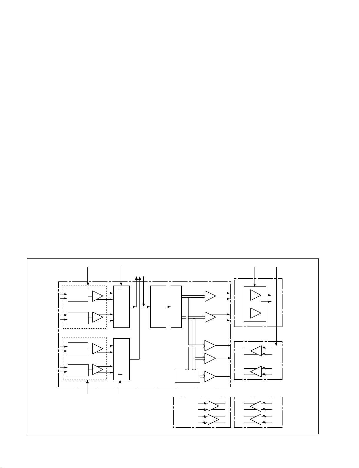
1-2-6. Audio System
Block structure
Front microphone amp : MA-162 board
Input signal selector : FP-157 board
A/D circuit (CH1&2) : FP-157 board
A/D circuit (CH3&4) : FP-157 board
D/A circuit : FP-157 board
Final amp : CNB-25 board
Monitor amp : FP-157 board
Rear input : AXM-38 board
DPS operation processing : DVP-45 board
1-12
PDW-700/V1 (E)
Page 23
1. Front microphone amp
The front microphone amp on the MA-162 board comes
with a gain switch. (30 dB/20 dB/10 dB)
Gain switching can be performed from the menu.
(_60 dBu/_50 dBu/_40 dBu)
2. Input signal selector
The audio signal can be selected with the analog switch
(IC1 to IC4) based on the side panel switch information.
3. A/D circuit
A/D uses 24-bit AK-5383. The sampling frequency is 48
KHz.
The first has an ATT circuit for head room level adjustment.
performed with the operational amp with electronic
volume (NJM2172).
7. Rear input
The rear input is composed of the following: a switch for
Line In, AES/EBU, and MIC-IN; +48 V ON/OFF-SW;
automatic detection circuit (DET-47 board) for the 3-pin
input XLR connector; and the microphone amp (10 dB/20
dB/30 dB).
Gain switching can be performed from the menu.
(_60 dBu/_50 dBu/_40 dBu)
Line In input level setting can be switched to +4 dBu,
0 dBu, or _3 dBu with the slide switch on the AXM-38
board. (Open the inside panel.)
4. D/A circuit
D/A uses 24-bit AK-4382A. The sampling frequency is 48
KHz.
The latter has a differential LPF circuit and an output level
amp circuit.
5. Final amp
The final amp is located on the CNB-25 board and is
connected to the AXM-38 board with the connector-toconnector. The CH1 and CH2 output signals are output
from the 5-pin XLR connector.
The output level can be selected as _3 dBu, 0 dBu, or +4
dBu from the menu.
6. Monitor amp
Composed of the monaural amp for the front earphone and
stereo amp for the rear earphone, the volume control is
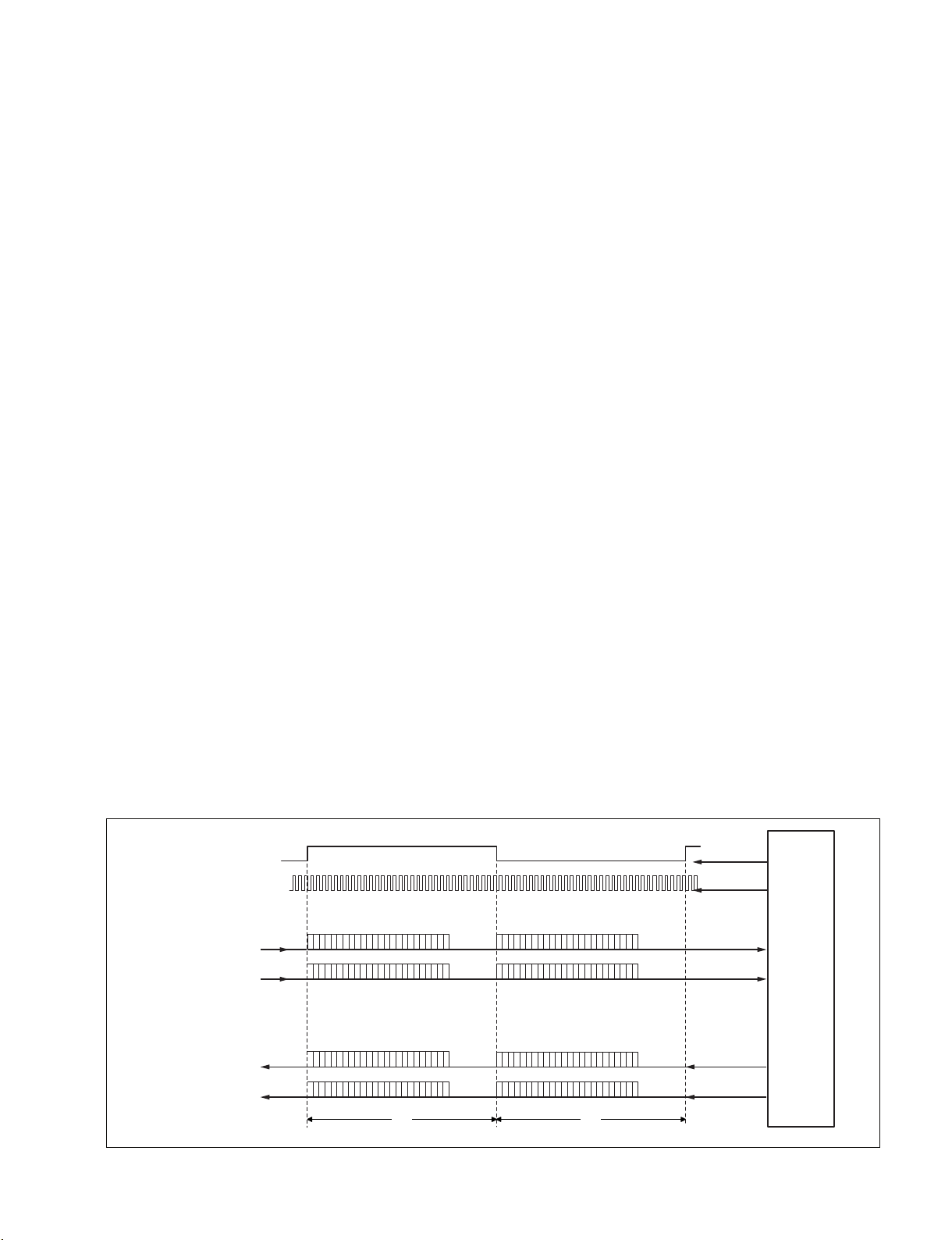
Fs
64Fs
Operation description
After the power to the device is turned on, each port in the
FP-157 board CPU is initialized, the necessary resistor data
is set, and MUTE is cancelled. (After approximately 3
seconds, the digital EE sound can be monitored.)
The front mic signal passes through the MA-162 board and
MB-1111 board before entering the input signal selector
(analog switch: IC1 to IC4) of the FP157 board.
The rear input signal passes through the AXM-38 board,
CNB-25 board, and MB-1111 board before entering the
input signal selector (analog switch: IC1 to IC4) of the FP157 board.
The information from the FRONT/REAR/WIRELSS
switch position can be obtained by loading the three
Fs
64Fs
A/D OUT CH3&4 (24bit)
A/D OUT CH1&2 (24bit)
(Left Justified,24bit Data)
D/A IN CH3&4 (24bit)
D/A IN CH1&2 (24bit)
(Left Justified,24bit Data)
PDW-700/V1 (E)
23
MSB
23 0
MSB
23 0
MSB
23 0
MSB
32bit
A/D & D/A Signal Format Diagram
0
23 0
MSB
CH3
23 0
MSB
CH1
23 0
MSB
CH3
23 0
MSB
CH1
32bit
CH4
CH2
CH4
CH2
AN34
AN12
DA34
DA12
DVP-45
1-13
Page 24
signals from the switch connected to each A/D terminal in
the FP_CPU (S1 to S4).
FP_CPU sends the switch position information to
ITORN_CPU of the SY-355 board, and then selects the
audio signal by receiving the audio mode information from
the ITORN_CPU.
The selected CH1 and CH2 system signals enter the
differential amp (IC5: balance-to-unbalance converter) and
pass through the head room level switching circuit and
balance-to-unbalance conversion amp for A/D. Then, the
signals are applied to the A/D converter IC (IC102: 24-bit).
The serial digital audio signal (2 channels) converted to
digital is entered to VAX (IC200) of the DVP-45 board via
the MB-1111 board
VAX (IC400) selects the entered digital audio signal and
sends it as the recorded audio data to AUDIO REC DSP
(IC800).
DSP for audio performs high-speed processing for
operations such as gain processing during manual
operations, AUTO processing, LIMITER processing, 67
Hz notch filter while using the front mic, LPF (15 KHz)
ON/OFF, internal SG, and audio level detection.
combined front and side volumes and sends the results to
DSP.
The D/A serial signal for playback passes through the
DVP-45 board and MB-1111 board and enters the digital
switch (IC461) of the FP-157 board. In the monitor CHSW, CH1&2 or CH3&4 is selected and applied to the 24bit D/A converter (IC453).
The D/A converter output passes through the differential
LPF, ATT balance-to-unbalance conversion amp (IC514),
and MB-1111 board. It is applied to the final amp (IC200,
IC201) of the CNB-25 board and output from the 5-pin
XLR connector (AXM-38 board).
The audio signal for the monitor passes from IC520/620
output through the monaural, mix, and stereo switching
switch (IC703, IC704). Then, the signal is applied to the
operation amp (NJM2172) with electronic volume.
The rear earphone can be switched between stereo and
mono from the menu.
The monitor speaker output level can be lowered from the
volume. Select one of the following for the ATT value: 0,
_3 dB, _6 dB, or _9 dB.
On the other hand, the front volume and side volume are
connected to the A/D terminal in the CPU and the volume
voltage is converted into digital with the internal 10-bit A/
D. After being converted into a multiplication value for
DSP, the signal is sent to ITORN_CPU.
ITORN_CPU performs operation processing on the
InPut
24dBu
20dBu
10dBu
+4dBu
+0dBu
_3dBu
_10dBu
_20dBu
_30dBu
_40dBu
_50dBu
_60dBu
_17dB
WireLess
_40dBu
_50dBu
_60dBu
_20dB
Max Input : _20dBu
Digital_WRR;
Reference OUT : _40dBFS
(DSP setting the same MIC
as specifications)
12dB:ATT 0dB
_24dB
Max Input : _10dBu
16dB:ATT 4dB
18dB:ATT 6dB
20dB:ATT 8dB
_20dBu
_30dBu
MIC
Max Input : 0dBu
HeadRoom
Tp-1
_21dBu
_31dBu
I2S-Format
_40dBFS
AK5383
40dB
30dB
Tp-101
_29dBu
_39dBu
HeadRoom : Get 30dBu
AK-5383 input : _23dBu
(X, Y terminal : _29dBu)
HeadRoom : Get 40dBu
AK-5383 input : _33dBu
(X, Y terminal : _39dBu)
LINE-IN;
MIC-IN;
24bit
A/D
_30dBFS
_40dBFS
DSP
(TMS320DA150GGU120)
_20dBFS
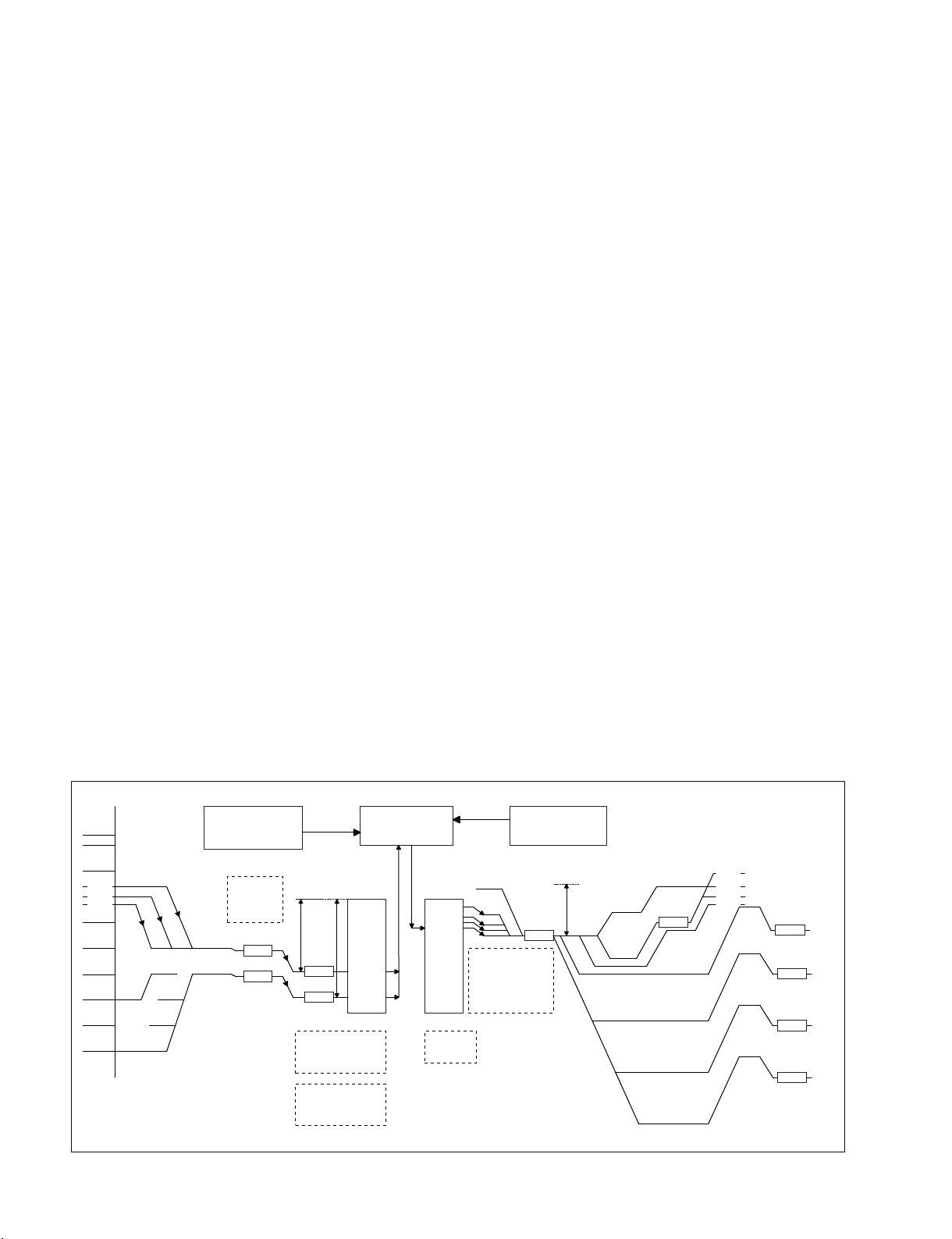
1-2-7. Audio DSP Operation Processing
Main functions
1. AUTO-AMP: Two to four types of characteristics can
be selected depending on each headroom.
_4dBu
_8dBu
_10dBu
_12dBu
AK4382A
24bit
D/A
AK-4382A
Max Output;
±
2.75Vp-p
_20dBFS
ALARM-TONE
CPU_OUT:2.7dBu
_3dB
HeadRoom
_12dB:ATT 8dB
_16dB:ATT 4dB
_18dB:ATT 2dB
_20dB:ATT 0dB
(Controled ATT of DAC)
AES/EBU;
Reference OUT : _20dBFS
+5dBu
_17.5dB
Tp-500
_15dBu
20dB
_33dB
_15dB
+9dB
_9dB
_12dB
VR_Max:_30dBu
VR_Max:_48dBu
ALARM_VR(Min):Faint_On
Tp-501
_10dBu
+14dB
ALARM_VR(Min):Faint_Off
+9dBu
+4dBu
+0dBu
_3dBu
+26dB
+26dB
+26dB
+26dB
_4dBu
_22dBu
XLR-OUT
(IN : +24dBu, Limiter-ON)
(IN : +4dBu, AGC-ON)
_13dBu
HeadPhone
(8Z loded)
_31dBu
ALARM (Max)
_62dBu
ALARM (Min)
Faint : On
_90dBu
ALARM (Min)
Faint : Off
1-14
Audio Level Chart
PDW-700/V1 (E)
Page 25
AGC/LIM SPECIFICATION
0
_
10
_
20
_
40
_
30
_
50
_
60
_
70
0 +10 +20
_
10
_
20
_
30
_
40
_
50
_
60
_
70
_6dBFS
_9dBFS
_15dBF S
_12dBF S
_17dBF S
INPUT [dBFS]
OUTOPUT [dBFS]
_8.1
dBFS
_11.4
dBFS
_14.6
dBFS
_17.9
dBFS
_20.0
dBFS
Output level at 0dBFS input.
Subthreshold level
_5.4dBFS max
_8.4dBFS max
_11.4dBFS max
_14.4dBFS max
_16.4dBFS max
_4.8dBFS max
_7.8dBFS max
_10.8dBFS max
_13.8dBFS max
_15.8dBFS max
0dBFS
Features of the AGC/LIM OFF.
: Features in common of the MIC/LINE input.
Max input level
of the LINE input.
Max input level
of the MIC input.
2. LIMITER characteristics: Two to four types of
characteristics can be selected depending on each
headroom.
3. OUT_PUT_LIMITER characteristics: Performs
LIMITER processing on the PB and EE_OUT. ON/
OFF.
4. Turns on and off the HPF (67 Hz) and LPF (15 KHz;
_24 dB). (Runs automatically during front
microphone selection)
5. Performs gain control when CH1 and CH2 are on
MANUAL status. (VR-MAX: +12 dB)
6. CH3 and CH4 turn on and off the AUTO operation.
7. Internal SG: Four types of 1 KHz/_12, _16, _18,
_20 dBFS.
8. Recording error correction: +0 to _2 dB (started from
the terminal)
9. Playback error correction: +0 to _2 dB (started from
the terminal)
10. INPUT delay amount: Performs delay processing to
match the VIDEO and AUDIO phases of each CH.
Description of each part
1. DIGITAL AUTO_AMP Processing
Selects the AUTO level from the menu.
AU AUTO SPEC : _6 dB/_9 dB/_12 dB/_15 dB/_17 dB
_6 dB : Linear operation until approx. _9 dBFS. Approx.
_6 dBFS at Max.
_9 dB : Linear operation until approx. _12 dBFS.
Approx. _9 dBFS at Max.
_12 dB : Linear operation until approx. _15 dBFS.
Approx. _12 dBFS at Max.
_15 dB : Linear operation until approx. _18 dBFS.
Approx. _15 dBFS at Max.
_17 dB : Linear operation until approx. _20 dBFS.
Approx. _17 dBFS at Max.
2. DIGITAL In Put LIMITER characteristics (only
during MANUAL)
Selects the LIMITER level from the menu.
AU AUTO SPEC : _6 dB/_9 dB /_12 dB/_15 dB/_17 dB
_6 dB : Linear operation until approx. _9 dBFS. Approx.
_9 dB : Linear operation until approx. _12 dBFS.
_12 dB : Linear operation until approx. _15 dBFS.
_15 dB : Linear operation until approx. _18 dBFS.
_17 dB : Linear operation until approx. _20 dBFS.
PDW-700/V1 (E)
_6 dBFS at Max.
Approx. _9 dBFS at Max.
Approx. _12 dBFS at Max.
Approx. _15 dBFS at Max.
Approx. _17 dBFS at Max.
3. DIGITAL Out Put LIMITER characteristics
Turn the LIMITER ON/OFF from the menu.
ON : Linear operation until approx. _12 dBFS, approx.
_11 dBFS (at Max.)
OFF : Turn off LIMITER at 0 dBFS.
4. Gain control during MANUAL
The A/D converted VR value is converted into a DSP
multiplication value at FP_CPU and synchronized with the
VIDEO1 frame, then handed over to the CPU to set in the
register of the DSP. The maximum variable for volume is
+12 dB. (_∞ to +12 dB)
5. Recording error correction
For error correction on the A/D converter for audio, the
multiplication value is corrected in the range +0 to _2 dB.
Starts from the terminal with the standard signal level
applied. (fully automatic)
6. Playback error correction
For error correction on the D/A converter for audio, the
multiplication value is corrected in the range +0 to _2 dB.
The correction is performed after the playback error
correction is completed. Starts from the terminal. (semiautomatic)
The internal SG is used as the standard signal, and the
inside panel for each LEVEL_VR is turned and fine-tuned.
1-15
Page 26

1-2-8. Optical Drive System
Recording System
Recording data sent from the DVP-45 board through the
ATA bus (Ultra ATA33) is sent to the Blu-ray Disc
Controller (BDC) IC300 on the DR-606 board.
The BDC performs signal processing to conform to
recording format, such as ATA interface, ECC coding and
17PP (Parity Preserve/Prohibit RMTR) modulation.
The recording data is converted to multi-pulse in the BDC,
and the multi-pulse data is sent through the flexible card
wire to the optical block to be written into the disc.
Playback System
• Data Playback System
The RF signal played back from the disc is sent from the
optical block to the Front End Processor (FEP) IC200 on
the DR-606 board where equalizing and asymmetry
correction are performed after the RF signal passes
through the AGC. After A/D conversion by the read
clock played back in the PLL, the signal is sent to the
BDC IC300.
In the BDC, the signal passes through the adaptive
digital filter, and Viterbi demodulation, 17PP demodulation, and ECC decoding are applied to the signal. Then
the signal is sent through the ATA bus to the DVP-45
board as played back data.
The tilt actuator is controlled for its angle against the
disc to be optimum based on the tilt adjustment result for
the jitter of the playback signal to be minimum and the
output of the angular velocity sensor.
The SA actuator position is controlled for the spherical
aberration to be optimum at the start-up adjustment when
the disc is inserted. The SA actuator for the double layer
disc is controlled to the optimum position every time to
jump the layer.
• Seek Motor
The seek motor controls the position of the optical block
so that the track to be recorded or played back is kept
within the object lens driving range.
• ND Filter
The transmission factor of the ND filter is selectable to
reduce the laser noise that occurs when the read power
light is emitted for the single layer disc.
• Spindle Motor
The FG generated by the spindle motor is amplified and
shaped on the SE-857 board, and is then input into the
SV DSP IC400 on the DR-606 board.
The SV DSP compares the FG frequency with the target
frequency, and then controls the spindle motor via the
driver IC500.
• Address restoration system
The address data restored from the disc is sent from the
optical block to the FEP (IC200) on the DR-606 board.
The analog address data passes through the AGC and
BPF and is converted to digital data in the FEP. The
digital data is then sent to the BDC (IC300) for address
decoding.
The PLL in the FEP generates a wobble clock (WCK).
Servo System
• Tri-Axis Actuator and SA Actuator
The object lens of the optical block is controlled for
focus direction, track direction, and tilt angle by the tri
axis actuator.
The light reflected from the disc is converted to the
electrical signal by the optical block. The electrical
signal is input to the FEP IC200, and the focus error
signal and the track error signal are detected. The SV
DSP IC400 outputs the control data based on the errors
to the driver IC501 and controls the focus actuator and
the track actuator through the driver.
System Control
The SY CPU IC600 on the DR-606 board performs system
control. It controls ATA interface, Data Manager, RFrelated ICs, servo ICs, and loader. It also carries out
interlocking control, maintenance and error log
management of each device including the optical block.
Firmware programs of the SY CPU and DSP as well as
sources of each PLD are stored in the flash memory IC602,
and the CPU loads them to each device when the power is
turned on.
The BDC IC300 and SV DSP IC400 are controlled by the
parallel CPU bus, while RF-related ICs are controlled by
the serial port through SYS PE IC700.
Adjustment values and hours meter data are stored in the
EEPROM IC4 on the SE-857 board.
1-16
PDW-700/V1 (E)
Page 27

1-2-9. Power Supply Systems
the input power is set to below 18 V.
CNB-25 board
The board checks the input voltage +12 V, and controls
distribution of the input power to each circuit board.
• Power ON/OFF Control
The ON/OFF control is performed in IC1 and IC5. The
IC1 input signals include L PWR SW ON signal, H
POWERW HOLD signal, EXTDC detection signal,
battery detection, excess voltage detection, and low
voltage detection. During normal operation, when L
PWR SW ON signal is turned to “L”, Q4, 5, 6, and 7 or
Q11, 12, 15, and 16 are turned on, and the battery or
EXT DC IN +12 V is supplied to respective circuit. The
H POWERW HOLD signal is sent from the FP-157
board after the main power of this unit is turned on.
Therefore, the power is kept on even if the L PWR SW
ON (L) signal is set to OFF (H). In order to turn off the
main power of this unit, the L PWR SW must be turned
off (H) and the H POWERW HOLD signal must be
opened and set to “L”. When the FP-157 board detects
that the POWER switch is turned OFF, it sets the
POWERW HOLD signal to “L” to turn off the power
after a disc operation is completed if the equipment is in
the midst of operating a disc.
• Battery/EXT DC selector
The EXT DC voltage is detected and either battery or
EXT DC is selected with priority given to the EXT DC.
The IC5 performs the control and Q4, Q5, Q6, and Q7
are turned on when a battery is selected and Q11, Q12,
Q15, and Q16 are turned on when the EXT DC is
selected.
In this IC5, a step-up circuit (Vcc +8.5 V) that drives the
N-CH MOS FET gate is employed.
• Excess current detection
The output circuit of the UNREG +12 V has excess
current detection resistors R70, R71 and R72. A voltage
drop at the resistors is detected by the IC5.
When the voltage drop at the resistors exceeds 200 mV,
the +12 V output is turned off.(SHUT DOWN)
Another SHUT DOWN signal is the H SHUT DOWN
signal that is supplied from the RE-246 board. If any one
of the DC-DC converter outputs is shorted, the output 12
V enters the SHUT DOWN state except UN SW +12 V.
(SHUT DOWN)
Since this function is a latch operation, the main power
of the unit needs to be turned off once and back on after
the cause of the excess current is removed.
• Protection against input power connection of reverse
polarity
If the input power is connected in reverse polarity, FET
(Q2) is turned off so that the GND lines of the control
system circuits are disconnected. Thus the control
circuits are protected and supply of +12 V power to the
respective circuits is stopped.
• FAN voltage control
The Q13 and Q14 are controlled by the FAN CONT
signal from the AT-177 board and the PWM wave is
converted to the DC voltage according to the DUTY.
The voltage controls the FAN and reduces the temperature increase.
• Audio Circuit
This is the output circuit for the AUDIO OUT (rear
connector). The signal is output by selecting the CH1/2
or CH3/4 in the MONITOR.
• Protection from Excess Input Voltage
VOLTAGE DETECT (IC18) monitors the input +12 V.
If the voltage exceeds approximately +18 V, the output
of the IC18-1 is set to “H”. This is input to IC1 to start
the protection from the excess voltage and turn on the
+12 V output. (SHUT DOWN)
Since this function is a latch operation, the main power
of the unit needs to be turned off once and back on after
PDW-700/V1 (E)
• ± 4.8 regulator circuit
This is the voltage regulator for AUDIO using on the
AXM-38 board.
1-17
Page 28

1-2-10. LCD System
PD-118 board
The PD-118 board consists of the color LCD panel drive
circuit and the power supply circuit for LCD backlight.
IC1 is the color LCD panel drive IC that contains of the
built-in video signal RGB driver, the timing generator, and
the VCO.
IC1 also contains the serial interface circuit and electronic
potentiometers that are used to establish the various setups
in accordance with the commands from the microprocessor
(IC921) of the FP-157 board.
The RGB video signals that are input to IC1 pin-37
through pin-39 receive contrast adjustment and brightness
adjustment. Then, they pass through the output signal
polarity inversion circuit and are output from IC1 pin-20
through pin-22.
The factory adjustment data is stored in the IC3 EEPROM.
The respective timing signals for driving the LCD panel
are generated from the sync signals that are input to IC1
pin-41 and pin-42.
The operations such as turning off the backlight and
inverting the video signal left to right or up to down are
performed in accordance with the control signals supplied
from the microprocessor (IC921) of the FP-157 board.
LOW so that the camera microprocessor checks capacity
and types of the memory stick inserted.
VCC is supplied to a memory stick only when a memory
stick is inserted or only when accessing a file on a memory
stick. When VCC is supplied, the INS_LED and
ACTIVE_LED (D1) is turned ON.
Access to the memory stick data is processed in the
following order: VCC IN → SCLK ON → BS Pulse →
DATA IN/OUT → SCLK OFF → . . → SCLK ON →
BS ON → DATA IN/OUT → SCLK OFF → . . → VCC
OFF.
1-2-11. Others
CN-3005 board
The VF power supply, light power supply, light switch
signal, and the EEPROM circuit that stores the rely and
system information of the handle switch signal are
included.
Handle switch relay
Input and output the handle switch signal (CN2).
Light switch relay
Relays the light switch signal (CN3).
EEPROM
The system information is written to the EEPROM (IC2)
by the I2C communication to control.
MS-86 board
The MS-86 board is the connector board for the memory
stick connection.
When a memory stick is inserted, the INS signal is set to
1-18
PDW-700/V1 (E)
Page 29
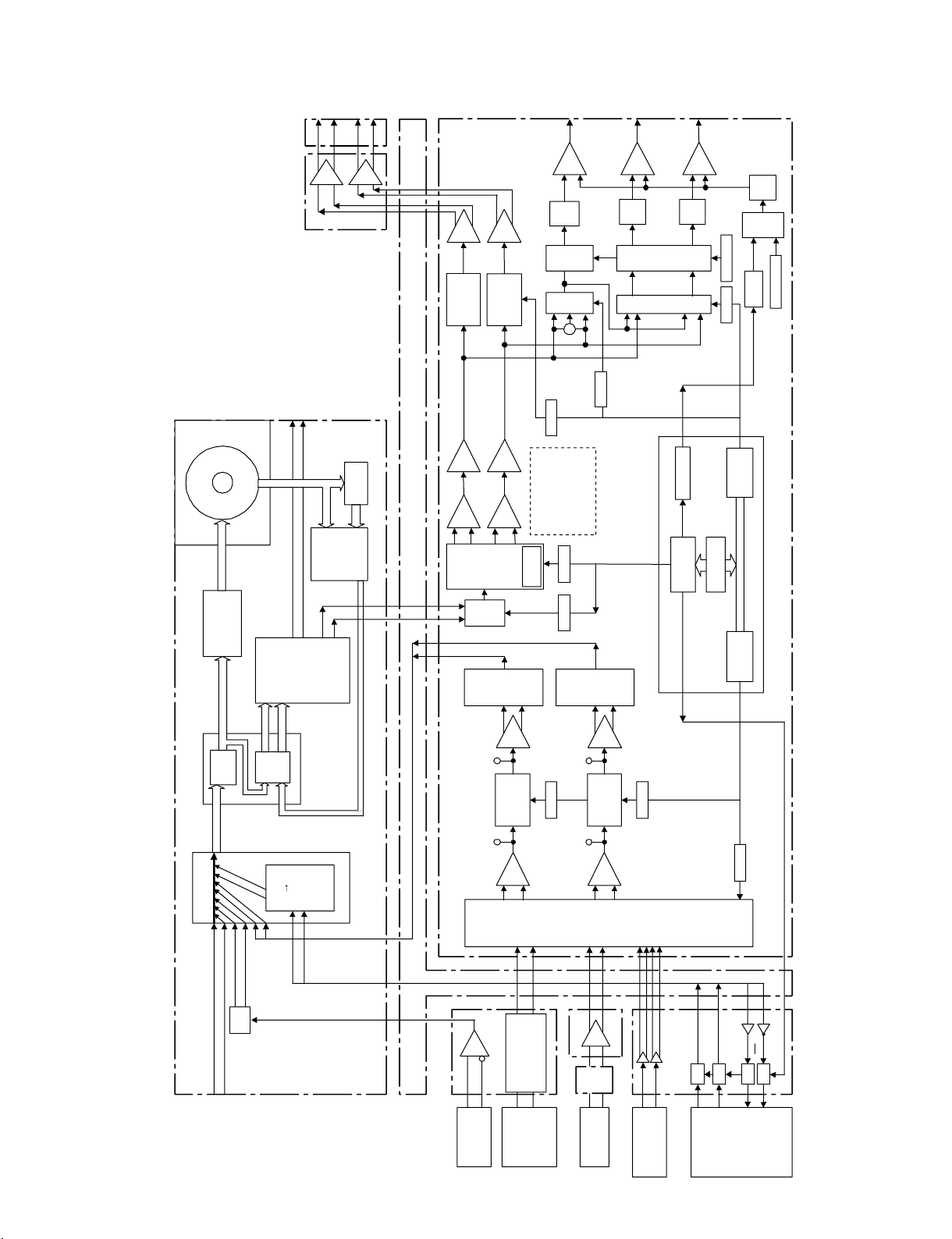
HeadRoom
SW
0dB
X
Y
_1dB
Tp1
Tp2
Tp101
Tp201
AK-5383
24bit A/D
HeadRoom
SW
0dB
X
Y
_1dB
Tp3
Tp4
Tp301
Tp401
AK-5383
24bit A/D
Differential Amplifier
(Balanced/Unbalanced)
X
Y
AK-4382A
24bit D/A
SW
X
Y
X
Y
X
Y
X
Y
X
Y
ATT _17,_20,_24dB
AMP10dB,20dB,30dB
LINE IN : 4dBu
+0dBu
_3dBu
MIC IN : _40dBu
_50dBu
_60dBu
AES/EBU
MIC IN : _40dBu
_50dBu
_60dBu
XLR
5P
AMP
10dB/20dB/30dB
RS-422
Receiver
_3dB
LPF
I2S_Format
RX-101
Analog-Wireless
2ch Adapter
_40dBu 25Z
Digital-Wireless
Adapter
_40dBFS
AUDIO_FORMAT:
I2S
OR
OR
XLR REAR
XLR Front
0dB
ATT
0dB
_9dB
_12dB
CH2 : _15dBu
+4dB
0dB
_3dB
CA D12
CA D34
SRC
AES/EBU D12
AES/EBU D34
Digital WRR D12
Digital WRR D34
AU D12
AU D34
VAX
DE_MUX
ANA OUT D12
ANA OUT D34
Low Reso
4ch
REC
PB
DSP(120MHz)
TM320DA150GG120
DE_MUX
PB
Rec 4ch
32BIT x 4ch
EE
32BIT x 4ch
Digital OUT D12
Digital OUT D34
PB 4ch
PB 4ch
DE_MUX
I2C BUS
PCA9555 PCA9555
MB -1111
MB -1111
SW
NJM
368M
4dB
AXM-38
CNB-25
XLR 5P
OUT
AXM-38
FS
64FS
Digital WRR D12
Digital WRR D34
MA-162
+
SW
NJM
368M
NJM
368M
CH1
CH2
CH1
CH2
FRONT
HeadPhone
& MONITOR_SP
REAR
Stereo
HeadPhone
NJM
2172
VCA
_95dB
VR-Control
Audio System Control
FP CPU
HD64F2378
14dB
FP-157
PCA9564
AUDIO
SELECT
Control
Control
Control
Control
Control
Control
NJM
2172
VCA
_95dB
VR-Control
ALARM-TONE
HaedRoom
ATT
Ch2
Ch1
CN-3001
Control
Control
24bit_I2S
Left
Justified
24bit
Data Cnv.
SW
SW
NJM
2172
VCA
_95dB
ATT
15dB
ATT
15dB
SW
SW
ATT
15dB
ATT
17.5dB
ATT
33dB
_15dBu
HeadRoom
_12dB:ATT 8dB
_16dB:ATT 4dB
_18dB:ATT 2dB
_20dB:ATT 0dB
(Controled ATT of DAC)
_3dB
LPF
X
Y
0dB
CH1 : _15dBu
ATT
0dB
_9dB
_12dB
4dB
14dB
DVP-45
Audio Block Overview
PDW-700/V1 (E)
1-19
Page 30
1-3. Matching Connectors
DC IN : XLR, 4-pin (Male)
Use the following connectors at the ends of the cables
when connecting the cables during installation and maintenance, or alternately use the following cables.
Panel indication Matching connectors/cables
GENLOCK IN
TC IN 1-569-370-12
TC OUT Plug, BNC
TEST OUT
SDI IN
SDI OUT 1
SDI OUT 2
AUDIO IN CH1/CH2 1-508-084-00 XLR 3-pin, male
AUDIO OUT Audio cable
(XLR 5 pin-XLR 3-pin, 2 m)
CCXA-53 made by Sony or equivalent
DC IN 1-508-362-00 XLR 4-pin, female
DC OUT 12 V 1-566-425-11 round type 4-pin, male
EARPHONE Mini jack (commercially available
on market)
LIGHT Power tap (OE)
Made by ANTONBAUER Inc.,
33710 or equivalent
MIC IN 1-508-370-11 XLR 5-pin, male
NETWORK 100 BASE-TX
REMOTE 1-766-848-11 round type 8-pin, male
VF Connector, 20-pin, male
Hirose HR 12-14PA-20PC or equivalent
i.LINK DV cable (6-pin-4-pin) : CCFD-3L
DV cable (6-pin-6-pin) : CCF-3L
WIRELESS WRR-855A, DWR-S01D (by Sony) only
RECEIVER IN connectable
n
Do not connect with a connector/
cable other than above.
1-4. Signal Inputs and Outputs
1
__
_ EXT VIEW
__
No. Signal I/O Specifications
1 GND _ GND for BATT OUT (+)
2 _ No connection
3 _ No connection
4 BATT OUT (+)IN +11 to 17 V dc
4
23
__
_
__
AUDIO IN CH-1, CH-2 : XLR, 3-pin (Female)
2
__
_ EXT VIEW
__
1
3
__
_
__
(0 dBu = 0.775 V rms)
MIC/LINE INPUT
No. Signal I/O Specifications
1 MIC/LINE (G) __60 dBu/+4 dBu, selectable
2 MIC/LINE (X) IN
3 MIC/LINE (Y) IN
High impedance, Balanced
AES/EBU INPUT
No. Signal I/O Specifications
1 AES/EBU (G) _ 1 Vp-p, 110 Z, Balanced
2 AES/EBU (X) IN
3 AES/EBU (Y) IN
Inputs
GENLOCK IN : BNC type 1.0 V p-p, 75 Z unbalanced
TC IN : BNC type 0.5 V to 18 V p-p, 10 kZ
SDI IN (Option) : BNC type
Outputs
TEST OUT : BNC type 1.0 V p-p, 75 Z unbalanced
SDI OUT : BNC type SDI 0.8 V p-p, 75 Z,
270 Mbps, 1.5 Gbps
TC OUT : BNC type 1.0 V p-p, 75 Z
EARPHONE : 8 Z or more, _∞ to _18 dBu variable
1-20
PDW-700/V1 (E)
Page 31

DC OUT 12 V : DIN, 4-pin (Female)
14
32
LENS : 12-pin (Female)
7
8
6
9
0
5
1
2
3
!-!=
4
__
_ EXT VIEW
__
__
_
__
No. Signal I/O Specifications
1 UNREG GND _ GND for POWER
2 _ No connection
3 _ No connection
4 UNREG +12 V OUT +11 to 17 V dc
AUDIO OUT : XLR, 5-pin (Male)
1
2
__
_ EXT VIEW
__
5
4
3
__
_
__
(0 dBu = 0.775 V rms)
No. Signal I/O Specifications
1 ANALOG GND _
2 AUDIO CH-1 (X) OUT 0 dBm (600 Z terminated)
3 AUDIO CH-1 (Y) OUT
4 AUDIO CH-2 (X) OUT
5 AUDIO CH-2 (Y) OUT
__
_ EXT VIEW
__
__
_
__
No. Signal I/O Specifications
1 RET (SW) IN ON : 0 V, OFF : OPEN
2 VTR TRIG IN ON : 0 V, OFF : OPEN
3 LENS GND _
4 AUTO +5 V OUT AUTO : +5 V,
MANU : 0 V or OPEN
5 IRIS CONT OUT +3.4 V (F16) to +6.2 V (F2.8)
6 UNREG +12 V OUT +11 V to 17 V
7 IRIS PSTN IN +3.4 V (F16) to +6.2 V (F2.8)
8 REMOTE/LOCAL OUT AUTO IRIS : 0 V
MANUAL IRIS : +5 V
9 EXTENDER IN EX 2 ON : 0 V
EX 0.8 ON : +1.8 V
OFF : +4.8 V
10 ZOOM PSTN IN WIDE : 2 V, TELE : 7 V
11 LENS RX
12 LENS TX
LIGHT : 2-pin (Female)
12
BATT IN : 5-pin (Male)
12345
__
_ EXT VIEW
__
No. Signal I/O Specifications
1 BATT (_)IN
2 BATT ID IN
3 BATT REM IN
4 LIGHT CONT OUT
5 BATT (+)IN+11 to 17 V dc
PDW-700/V1 (E)
__
_
__
__
_ EXT VIEW
__
__
_
__
No. Signal Specifications
1 LIGHT +12 V OUT 50 W MAX
2 GND
1-21
Page 32

WIRELESS RECEIVER IN : D-sub, 15-pin (Female)
VF : 20-pin (Female)
8
15
__
_ EXT VIEW
__
1
9
__
_
__
No. Signal I/O Specifications
1 GND _ GND for AUDIO IN
2 Audio CH1 IN IN WIRELESS RECEIVER
AUDIO CH1 IN
3 Audio CH2 IN IN WIRELESS RECEIVER
AUDIO CH2 IN
4 DC +7 V OUT OUT
5 GND _
6 SCLK OUT 64 FS
7 WRR855 DET I/O
8 GND _
9 WRR CLK IN WRR SERIAL CLOCK
10 CS OUT WRR SELECT
11 WRR DI OUT WRR SERIAL IN
12 WRR DO IN WRR SERIAL OUT
13 LRCK OUT FS
14 DATA 1/2 IN AUDIO DATA 1/2 IN
15 DATA 3/4 IN AUDIO DATA 3/4 IN
i.LINK : 6-pin
2 4 6
1 3 5
__
_ EXT VIEW
__
__
_
__
__
_ EXT VIEW
__
__
_
__
No. Signal I/O Specifications
1 SDA VF I/O TTL level
2 _ No connection
3 _ No connection
4 SCL OUT TTL level
5 _ No connection
6 _ No connection
7 _ No connection
8 G TALLY OUT ON : 5 V, OFF : GND
9 _ No connection
10 _ No connection
11 _ No connection
12 VF VIDEO OUT 1.0 V p-p, Zo = 75 Z
13 VF VIDEO GND _ GND for VIDEO
14 VF VIDEO (Pb) OUT ± 0.35 V p-p, Zo = 75 Z
15 VF VIDEO (Pr) OUT ± 0.35 V p-p, Zo = 75 Z
16 _ No connection
17 R TALLY (UP) OUT ON : 5 V, OFF : GND
18 _ No connection
19 UNREG GND _ GND for UNREG
20 UNREG OUT +11 V to 17 V
No. Signal I/O Specifications
1 VP IN BUS POWER
2VG _ GND
3 NTPB I/O STROBE B (_)
4 TPB I/O STROBE B (+)
5 NTPA I/O DATA A (_)
6 TPA I/O DATA A (+)
1-22
PDW-700/V1 (E)
Page 33

REMOTE : 8-pin (Female)
MAINTENANCE
1
27
8
36
45
__
_ EXT VIEW
__
No. Signal I/O Specifications
1 TX RCP DATA (X) OUT SERIAL DATA OUT
2 TX RCP DATA (Y) OUT SERIAL DATA OUT
3 RX RCP DATA (X) IN SERIAL DATA IN
4 RX RCP DATA (Y) IN SERIAL DATA IN
5 VIDEO (G) _ GND for VIDEO
6 UNREG +12 V OUT +11 V to 17 V
7 UNREG (GND) _ GND for UNREG
8 VIDEO (X) OUT 1.0 V p-p, Zo = 75 Z
CHASSIS GND _ CHASSIS GND
__
_
__
MIC IN : XLR, 5-pin (Female)
5
4
__
_ EXT VIEW
__
1
2
3
__
_
__
(0 dBu = 0.775 V rms)
No. Signal Specification
1 MIC IN (G) _50 dBu High
2 MIC1 IN (X)
3 MIC1 IN (Y)
4 MIC2 IN (X)
5 MIC2 IN (Y)
impedance balance
1
4
No. Signal
1 USB_VBUS
2 USB_D_
3 USB_D+
4 GND
__
_ EXT VIEW
__
__
_
__
(NETWORK)
8
__
_ EXT VIEW
__
No. Signal I/O Specifications
1 TX (+) I/O Transmitted data (+)
2 TX (_) I/O Transmitted data (_)
3 RX (+) I/O Received data (+)
4 __No connection
5 __No connection
6 RX (_) I/O Received data (_)
7 __No connection
8 __No connection
1
__
_
__
PDW-700/V1 (E)
1-23
Page 34

1-5. On-Board Switch and LED Function
AT-177 board
S400
S401 S402
TOP menu
ON : To display the TOP menu
OFF : Not to display the TOP menu
ON : Service mode
(The SERVICE menu is displayed)
OFF : Normal mode
in “4-1-2. How to Display the SERVICE Menu”
ON : Disable
OFF : Enable
ON : Initializes the FRAM/AT-177 board
OFF : Normal mode
ABC
12345
Ref.No. Bit Name Function Factory setting
S400 __ Turns ON/OFF the function to display the ON
S501 1 _ Factory-use OFF
2 _ Factory-use OFF
3 _ Factory-use OFF
4 _ Factory-use OFF
S402 1 _ Service mode setting OFF
2 _ Disables displaying SERVICE menu by “Method 2” OFF
3 _ Factory-use OFF
4 _ Factory-use OFF
5 _ Factory-use OFF
6 _ Factory-use OFF
7 _ Factory-use OFF
8 _ FRAM initialization OFF
1-24
PDW-700/V1 (E)
Page 35

AXM-38 board
B
A
1
S101 S201
S203
2
Ref.No. Name Function Factory setting
S101 AUDIO IN (CH1) LINE/AES/EBU/MIC/(CH1) select switch
S201 AUDIO IN (CH2) LINE/AES/EBU/MIC/(CH2) select switch
*
*
_
_
S203 INPUT REFERENCE Sets the input reference level +4 dB
+4 dB : Sets the input reference level to +4 dB
0 dB : Sets the input reference level to 0 dB
_3 dB : Sets the input reference level to _3 dB
* : Refer to the “Operation Manual”.
DET-45 board
S1
Ref.No. Name Function Factory setting
S1 SW Color LCD turn switch _
DR-606 board
S600
Ref.No. Name Function Factory setting
S600 System reset Factory-use _
PDW-700/V1 (E)
1-25
Page 36

DVP-45 board
A
1
B
C
D
E
D1700
2
D2001
D2002
D2000
3
4
5
S900
D900
6
• Each LED is used for adjustment and check in the manufacturing process.
• S900, S1900, and S1901 are used for adjustment and check in the manufacturing process.
They are all set to off when shipped from the factory.
S1900
D2003
D901
D2004
D2005
D902
F
D2006
S1901
D2007
G
1-26
PDW-700/V1 (E)
Page 37

CN-2946 board
AB
D1
S1
1
2
Ref.No. Name Function Factory setting
D1 TALLY (Back tally) indicator Lights during recording when the TALLY switch is turned on*_
S1 TALLY switch Turns ON/OFF the TALLY indicator
* : Refer to the “Operation Manual”.
*
ON
CNB-25 board
A
1
2
D7
D6
D8
Ref.No. Name Function Factory setting
D6 Overvoltage protection Lights when the overvoltage protection starts to operate when the _
indicator input voltage of EXT DC or BATT reaches approx. 19.5 V or more.
D7 Low voltage protection Lights when the operation of the low voltage protection circuit of _
indicator CNB-25 board is repeated several times due to some error.
D8 Shut Down signal from Lights when the Shut Down signal is sent from the RE-246 board _
RE-246 due to a load error of the RE-246 board.
* : When the unit is shut down under the condition above this level, the overvoltage protection for the entire unit may start. In this case, the indicator does
not light.
B
This shuts down the unit
This shuts down the unit
This shuts down the unit
*
*
*
PDW-700/V1 (E)
1-27
Page 38

FP-157 board
S830
D845
S911
1
2
S10
S1
_
_
_
_
_
_
OFF
_
OFF
_
_
_
D842
D846
S20
S2
3
S3
S4
4
H
S701
S835
S703
S700
S702
S501
AB
S460
CD
S834
S840
S832
D843
S842
D844
S833
EF
S841
S843
S845
S837
S844
S846
S836
S831
S838
S839
G
Ref.No. Bit Name Function Factory setting
D842 _ WARNING Warning light. Lights when FP-CPU is abnormal
D843 _ THUMBNAIL Displays thumbnails
D844 _ SUB CLIP Lights during the clip playback
D845 _ TEST Lights during the FP-CPU initialization
*
*
*
D846 _ ACCESS Lights when the disc drive is being accessed
*
*
S1 _ CH1 FRONT/REAR/WRR FRONT
S2 _ CH2
S3 _ CH3
S4 _ CH4
S10 _ AUTO1 (ON:H/OFF:L) Selects the adjustment method of the audio level for audio _
channel 1
S20 _ AUTO2 (ON:H/OFF:L) Selects the adjustment method of the audio level for audio _
channel 2
S460 _ MONITOR Audio monitor select switch
*
*
*
(CH1/2, CH3/4)
S501 1 NC _ OFF
2NC _ OFF
3NC _ OFF
4 _ Turns on when 5P XLR of the AUDIO output of OFF
the AXM-38 board is changed to 3P
S700 _ ASSIGN2 Turns ON/OFF the assigned function
S701 _ CCC_SW Changes the color temperature
S702 _ ASSIGN1 Allocates the switch functions
S703 _ MONITOR Audio monitor select switch
*
*
*
*
*
(CH-L/MIX/CH-R)
S830 _ CPU_RESET Resets the CPU _
S831 _ BRIGHT* Brightness adjustment
S832 _ THUMBNAIL/ Thumbnail
*
*
ESSENCE MARK
1-28
PDW-700/V1 (E)
Page 39

Ref.No. Bit Name Function Factory setting
S833 _ SUB CLIP Plays the clip list
S834 _ HOLD/CHAPTER Displays the display hold/chapter function
S835 _ RESET Resets the time counter display
S836 _ SHIFT Shift
*
S837 _ DISPLAY Switches the counter display
*
*
*
_
_
_
_
*
(CTL/TC/U_BIT) COUNTER : Displays the counter for the elapsed
record/playback time
TC : Displays time-code
U_BIT : Displays user-bit
S838 _ F_RUN/SET/R_RUN F_RUN : Continuous time-code steps
*
SET : Sets the time-code and user-bit
R_RUN : Time-code steps while recording
S839 _ RESET/REGEN/CLOCK Reset/regenerate/expand button
S840 _ DISP SEL/EXPAND Switches the display contents
S841 _ UP UP
S842 _ LEFT LEFT
S843 _ SET/S.SEL SET
S844 _ RIGHT RIGHT
S845 _ DOWN DOWN
S846 _ CLIP MENU MENU
*
*
*
*
*
*
*
*
_
_
_
_
_
_
_
S891 1 _ Factory-use OFF
2 _ Factory-use OFF
3 _ Factory-use OFF
4 _ Factory-use OFF
* : Refer to the “Operation Manual”.
PDW-700/V1 (E)
1-29
Page 40

KY-623 board
D4
S7
S4
D3
S6
S3
D2
S1
S2
D1
S5
Ref.No. Name Function Factory setting
D1 FF Lights during fast-forward playback
D2 PLAY Lights during playback of the disc
D3 REW Lights during fast-rewind playback
D4 EJECT Blinks during disc ejection
S1 STOP Stops playback
S2 FF Fast forward
S3 PLAY Disc playback
S4 REW Fast rewind
*
*
*
*
S5 NEXT Moves to the next clip
S6 PREV Moves to the previous clip
S7 EJECT Ejects the disc
* : Refer to the “Operation Manual”.
*
*
*
*
*
*
*
_
_
_
_
_
_
_
_
_
_
_
MB-1111 board
C
B
S1
A
1
Ref.No. Bit Name Function Factory setting
S1 0 Normal boot Starts iTRON-CPU mandatorily in normal mode OFF
1 Recovery boot Starts iTRON-CPU mandatorily in recovery mode OFF
23456
1-30
PDW-700/V1 (E)
Page 41

MS-86 board
A
1
2
B
D1
Ref.No. Name Function Factory setting
D1 MEMORY STICK Lights when being accessed
* : Refer to the “Operation Manual”.
*
_
SW-1125G board
S1
Ref.No. Name Function Factory setting
S1 IN SENSE Cartridge presence OFF
S2 STBY OFF Cartridge chucking state OFF
S2
SW-1352 board
S1
Ref.No. Name Function Factory setting
S1 CH1 (ON/OFF) Turns ON/OFF the +48 V
S2 CH2 (ON/OFF) Turns ON/OFF the +48 V
* : Refer to the “Operation Manual”.
S2
*
*
OFF
OFF
PDW-700/V1 (E)
1-31
Page 42

SW-1391 board
S2S4S3
S1
S5S6
Ref.No. Name Function Factory setting
S1 VDR (SAVE/STBY) Switches the VDR operation state (SAVE/STBY)
S2 GAIN (L/M/H) Switches gain (L/M/H)
*
*
SAVE
L=0 dB, M=6 dB, H=12 dB
S3 WHITE BAL Switches the white balance memory PRST=3200K
(B-A-PRESET/ATW) PRST : Adjusts the color temperature to the preset value
A/B : Calls the saved white balance value
ATW : Switches the ATW operations
S4 OUTPUT Switches the output signal
(DCC : ON_OFF/BARS_CAM) Turns on/off the dynamic contrast control
BARS : Outputs the color bar signal
CAM : Turns on/off the DCC function
S5 MENU (ON/OFF) Turns on/off the MENU switch
S6 MENU (ON/OFF) Turns on/off the MENU switch
* : Refer to the “Operation Manual”.
*
*
*
*
*
*
_
OFF
OFF
SW-1425 board
S2
S3
S1
Ref.No. Name Function Factory setting
S1 REC START The button used to start/stop recording
*
_
S2 AUTO_W/B_BAL The switch used to automatically adjust white _
balance/black balance.
Turns on/off the electronic shutter
S3 SHUTTER Turns on/off the electronic shutter
* : Refer to the “Operation Manual”.
*
*
_
1-32
PDW-700/V1 (E)
Page 43

SW-1426 board
S1
Ref.No. Name Function Factory setting
S1 AUTO/MANUAL AUTO : Lights EXT LIGHT along with the REC operation
MANUAL : Turns ON/OFF EXT LIGHT manually
*
* : Refer to the “Operation Manual”.
*
_
SY-355 board
1
S200
S1301
S301
S1201
D
C
E
S1200
F
2
A
B
3
S300
4
5
D501
D500
D300
D301
D302
D303
D601
D600
D602
D603
6
• Each LED is used for adjustment and check in the manufacturing process.
• S200, S300, S1200, S1201, and S1301 are used for adjustment and check in the manufacturing process.
They are all set to off when shipped from the factory
D1304
D1305
G
D1302
D1303
D1301
D1300
PDW-700/V1 (E)
1-33
Page 44

1-6. How to Take Out a Cartridge
A
Manually
1-6-1. Taking Out a Cartridge at Power-off
1. Open the cover in the direction of the arrow A.
2. Push the lock lever in the direction of the arrow B with
a screwdriver. The cartridge lid assembly is opened in
the direction of the arrow C.
3. Rotate the gear counterclockwise with a crosshead
screwdriver to eject the cartridge.
If a cartridge cannot be taken out, turn the gear
clockwise until it will go and then turn it counterclockwise again.
m
. Turn the gear slowly and gently. Be careful not to
force the gear past their stopping points.
. Be sure not to touch or forcibly take out the cartridge
until it is completely ejected.
. Even when the cartridge cannot be ejected with this
procedure, do not rotate the gear with an excessive
force. This error may be caused by a problem in the
loader assembly.
In this case, refer to Section 1-6-2.
A
C
Cartridge lid
assembly
Cover
Flat-blade screwdriver
Lock
lever
B
Cross head (+)
screwdriver
Gear
1-6-2. When You Cannot Take Out a
Cartridge Even If Pressing the EJECT
Button at Power-on
1. Remove the outside panel. (Refer to Section 1-7-1.)
2. Remove the four screws and remove the laser caution
sheet.
3. Push the release pin in the direction arrow A, and pull
out the cartridge from the unit in the direction of the
arrow B.
n
Be careful not to touch the disc surface in the cartridge.
B2.6 x 5
B
Release pin
A
Laser caution
sheet
1-34
PDW-700/V1 (E)
Page 45

1-7. Removing/Installing
1-7-1. Removing Outside Panel
1. Open the cover in the direction of the arrow A.
2. Push the lock lever in the direction of the arrow B with
a screwdriver. The cartridge lid assembly is opened in
the direction of the arrow C.
3. Open the BNC cover in the direction of the arrow D.
4. Fully loosen the five screws (with drop-safe) of the
outside panel, and remove the outside panel in the
direction of the arrow E.
n
Close the cover securely after use.
1-7-2. Reinstalling Outside Panel
Cartridge lid
assembly
Screws
(with drop-safe)
Flat-blade screwdriver
Lock lever
Cover
A
B
1. Reinstall the outside panel to the unit with its cartridge
lid assembly opened, by tightening the five screws.
n
Do not tighten the screws with the cartridge inside. Be
sure to take out the cartridge before installing the
outside panel. (Refer to Section 1-6.)
2. Close the cartridge lid assembly.
3. Close the BNC cover.
1-7-3. Inside Panel
1. Fully loosen the four screws (with drop-safe) of the
inside panel, and open the inside panel.
2. Disconnect the flexible card wires from the four
connectors (CN105, CN106, CN107, CN801) on the
FP-157 board.
3. Remove the five screws of the FP cover, and remove
the inside panel.
D
BNC cover
C
E
Screws
(with drop-safe)
PSW2
x
5
PSW2
x
5
PDW-700/V1 (E)
PSW2
x
5
Screws
(with drop-safe)
CN107
CN106
CN105
FP-157 board
Inside panel
FP cover
CN801
Screws
(with drop-safe)
1-35
Page 46

1-7-4. Handle Assembly
1. Remove the inside panel. (Refer to Section 1-7-3.)
2. Remove the screw (B2.6 x 5) , and remove the
connector retainer.
3. Disconnect the CN-2947 board from the connector
(CN2) on the DCP-44 board.
4. Remove the two screws (B2.6 x 5) .
5. Disconnect the coaxial cables from the five coaxial
connectors (CN10, CN11, CN12, CN13, CN14) on the
DCP-44 board.
6. Disconnect the harness from the connector (CN3) on
the DCP-44 board.
7. Disconnect the harness from the connector (CN602)
on the AT-177 board.
8. Disconnect the DCP-44 board (The AT-177 board is
included.) from the connector on the MB-1111 board.
9. Disconnect the flexible card wire from the connector
(CN1300) on the SY-355 board.
10. Disconnect the harness form the connector (CN1500)
on the SY-355 board.
Flexible card wire
CN1300
SY-355 board
Harness
CN101
(MB-1111 board)
CN-2947 board
Harness
CN1500
CN2
CN3
B2.6 x 5
Yellow : CN10
Green : CN11
Blue : CN12
White : CN13
Red : CN14
Coaxial cable
DCP-44 board
CN13
CN10
B2.6 x 5
CN11
CN12
CN14
AT-177 board
Connector retainer
CN602
B2.6 x 5
11. Open the connector cover.
12. Remove the three screws (B2 x 5) , and remove the
tally cover.
13. Remove the two screws (B3 x 8) , and remove the
CN-2946/CN-3026 boards block assembly.
n
Be careful not to lose drop protection on the CN-2946
board, since it is not fixed.
Tally cover
Protection
CN-2946
board
CN-2946/CN-3026
board block assembly
rubber
B2 x 5
B2 x 5
Connector cover
B3 x 8
1-36
PDW-700/V1 (E)
Page 47

14. Remove the six screws (B3 x 8) .
15. Disconnect the harness from the connector (CN2) on
the CN-3005 board while slightly lifting up the handle
assembly, and remove the handle assembly.
1-7-5. Front Panel
1 Remove the outside panel. (Refer to Section 1-7-1.)
2. Remove the inside panel. (Refer to Section 1-7-3.)
3. Remove the screw, and remove the connector retainer.
4. Disconnect the CN-2947 board from the connector
(CN3) on the TG-260 board.
n
The CN-2947 board is fragile and can be easily
broken. Handle it with care.
5. Disconnect the harnesses from the three connectors
(CN2, CN4, CN6) of the TG-260 board.
6. Remove the four screws (B2.6 x 5) , and remove the
TG-260 board.
7. Remove the two screws, and remove the stay (OUT).
8. Remove the tape, and peel the GND sheet (OUT) from
the main frame.
n
The GND sheet can be broken during removal. Handle
it with care.
9. Remove the four screws (B3 x 8) .
10. Take off the front panel, disconnect the harness from
the two connectors (CN2, CN3) on the MS-86 board,
and remove the front panel.
Harness
CN2
(CN-3005 board)
Tapes
Stay (OUT)
B2.6 x 5
GND sheet (OUT)
Front panel
Harness
B3 x 8
B3 x 8
B3 x 8
B2.6 x 5
CN3
MS-86 board
CN2
B3 x 8
Harnesses
TG-260 board
B3 x 8
Handle assembly
Connector retainer
B2.6 x 5
CN-2947 board
CN6
B2.6 x 5
CN4
CN3
CN2
B2.6 x 5
PDW-700/V1 (E)
1-37
Page 48

1-7-6. SW Guard Assembly
1. Remove the outside panel. (Refer to Section 1-7-1.)
2. Remove the two screws to remove the SW guard
assembly.
n
If the loader has already been moved to the up position, the SW guard assembly may be difficult to
remove in some cases. Move down the loader by
rotating the gear in clockwise direction with crosshead
screwdriver.
Cover
Cross head (+)
screwdriver
Gear
Installation
Install the removed parts by reversing steps 1 to 2 of
removal.
1-7-7. Shoulder Pad, Connector Cover
1. Loosen the two pad screws, and remove the shoulder
pad.
2. Remove the four screws, and remove the connector
cover.
Note on installation:
After the shoulder pad is reinstalled, check the slide
operation. Check that it slides smoothly with the screws
fastened.
SW guard
assembly
PSW2 x 5
B3
x
A
B3
x
8
8
Connector cover
x
8
B3
LW3
Pad screws
1-38
Shoulder pad
PDW-700/V1 (E)
Page 49

1-7-8. Connector Panel Assembly
1. Remove the outside panel. (Refer to Section 1-7-1.)
2. Remove the inside panel. (Refer to Section 1-7-3.)
3. Remove the connector cover. (Refer to Section 1-7-7.)
4. Disconnect the coaxial cables from the two coaxial
connectors (CN11, CN12) on the DCP-44 board, and
detach the cables from the three hooks and the notch
on the MB-1111 board.
CN12
CN11
DCP-44 board
Coaxial cables
5. Remove the special screw (M2), and remove the drop
protection (XLR).
6. Disconnect the harnesses from the four connectors
(CN2, CN3, CN4, CN5) on the CNB-25 board.
7. Disconnect the flexible card wire from the connector
(CN7) on the CNB-25 board.
8. Remove the three screws (B2.6 x 5) , and disconnect
the CNB-25 board from the connector (CN1) on the
MB-1111 board.
9. Disconnect the harness from the connector (CN116)
on the MB-1111 board.
10. Disconnect the harness from the connector (CN1) on
the CN-2948 board.
11. Remove the two screws (B3 x 8) , and remove the
connector panel assembly.
Hooks
Special screw
(M2)
Harnesses
B3 x 8
Notch
(MB-1111 board)
CN2
CN1
( CN-2948 board )
Connector panel
Harness
CN3
CN4
CN7
B2.6
x
Drop protection
(XLR)
Flexible card
wire
Harness
CNB-25
board
x
B2.6
5
Harness
CN5
5
CNB-25
board
PDW-700/V1 (E)
Harness
CN116
(MB-1111 board )
CN1
(MB-1111 board )
1-39
Page 50

1-7-9. Rear Panel Assembly
1. Remove the outside panel. (Refer to Section 1-7-1.)
2. Remove the inside panel. (Refer to Section 1-7-3.)
3. Remove the connector cover. (Refer to Section 1-7-7.)
4. Remove the connector panel assembly. (Refer to
Section 1-7-8.)
5. Disconnect the coaxial cables from the two coaxial
connectors (CN10, CN13) on the DCP-44 board, and
detach the cables from the three hooks and the notch
on the MB-1111 board.
CN13
CN10
DCP-44 board
Coaxial cables
6. Disconnect the flexible card wire from the connector
(CN3) on the CI-37 board.
7. Remove the six screws (B3 x 8) , and remove the rear
panel assembly.
1-7-10. Battery Connector
1. Remove the outside panel. (Refer to Section 1-7-1.)
2. Remove the inside panel. (Refer to Section 1-7-3.)
3. Remove the connector cover. (Refer to Section 1-7-7.)
4. Remove the connector panel assembly. (Refer to
Section 1-7-8.)
5. Remove the rear panel assembly. (Refer to Section 17-9.)
6. Remove the four precision screws (B2.6 x 5), and
remove the battery harness assembly.
n
Be careful that the harness should not be caught or
damaged by any other part.
Hooks
Flexible card wire
Notch
(MB-1111 board)
Rear panel assembly
B3 x 8
CN3 (CI-37 board)
B3 x 8
Battery harness assembly
Precision screws
(P2.6 x 5, TYPE1)
1-40
PDW-700/V1 (E)
Page 51

1-8. Removing/Installing LCD Block
1-8-1. LCD Block
1. Remove the inside panel. (Refer to Section 1-7-3.)
2. Remove the two knobs (A).
3. Open the SW door (R) , and remove the two knobs (B) .
4. Remove the LCD harness holder.
5. Disconnect the harness from the six connectors
(CN700, CN701, CN702, CN703, CN802, CN850) on
the FP-157 board.
6. Remove the nine screws (PSW2 x 5) , and remove the
FP-157 board.
n
After removing the FP-157 board, be careful not to
drop the unfixed parts.
7. Remove the unfixed parts.
Harnesses
CN850
Knobs (A)
CN700
Harness
CN701
CN702
Harnesses
PSW2 x 5
Knobs (B)
SW door (R)
FP-157 board
CN802
CN703
PDW-700/V1 (E)
FP-157 board
Unfixed parts
PSW
2 x 5
LCD
harness holder
Inside panel
1-41
Page 52

8. Remove the four screws (PSW2 x 5) , remove the
LCD harness cover.
9. Remove the LCD harness through the hole of the
harness cover.
10. Remove the hinge blind plate and helical torsion
spring.
11. Remove the four screws (P2.6 x 6) , remove the inside
pad (L).
LCD harness
PSW2 x 5
LCD harness cover
P2.6 x 6
LCD harness cover
PSW2 x 5
Helical torsion
spring
Hinge blind plate
12. Remove the three screws (PSW2 x 5) , remove the
LCD block.
Inside pad (L)
LCD block
PSW2 x 5
PSW2 x 5
1-42
PDW-700/V1 (E)
Page 53

1-8-2. LCD Hinge
c
d
e
Back hinge cover
Front hinge cover
Hinge
Harness
DET-45
board
CN1
CN1
PD-118 board
LCD cover
LCD hinge
Harness
a
a
b
a
1. Remove the inside panel. (Refer to Section 1-7-3.)
2. Remove the LCD block. (Refer to Section 1-8-1.)
3. Remove the four screws of a (M2 x 4) , and remove
the LCD cover.
4. Remove the two screws of b (M2 x 4) .
5. Disconnect the harness from the connector (CN1) on
the PD-118 board, and remove the LCD hinge.
6. Remove the screw of c (M1.7 x 2.5) of the back
hinge cover, and remove the back hinge cover.
7. Turn the hinge and remove the two screws of d
(M1.7 x 2.5) , then remove the front hinge cover.
8. Disconnect the harness from the connector (CN1) on
the DET-45 board.
9. Remove the screw of a (M1.7 x 2.5) , and remove
the DET-45 board.
PDW-700/V1 (E)
1-43
Page 54

1-8-3. LCD Backlight and LCD Panel
1. Remove the LCD block. (Refer to Section 1-8-1.)
2. Remove the four screws a (M2 x 3) , and remove the
LCD cover.
3. Remove the two screws b (M2 x 3) .
4. Disconnect the harness from the connector (CN1) on
the PD-118 board, and remove the LCD hinge.
5. Disconnect the flexible card wire of the LCD panel
from the connector on the PD-118 board.
6. Release the six claws on the LCD bezel to remove the
LCD frame.
7. Remove the LCD panel from the LCD bezel.
a
b
LCD hinge
PD-118 board
LCD frame
LCD panel
LCD bezel
Harness
a
a
CN1
CN2
Claws
8. Disconnect the flexible card wire of the LCD backlight
from the connector (CN3) on the PD-118 board.
9. Remove the two screws c (M2 x 3) .
10. Release the hooks on the PD-118 board from the LCD
backlight to remove the PD-118 board.
11. Remove the three screws d (M1.7 x 2.5) .
12. Release the claws on the LCD backlight from the LCD
frame to remove the LCD backlight.
Hooks
PD-118 board
Claws
CN3
c
LCD backlight
d
Claws
LCD frame
LCD frame
LCD backlight
1-44
PDW-700/V1 (E)
Page 55

1-9. Replacing the Flat Cables, Flexible
A
A
A
A
A
A
A
A
A
A
A
A
Contact surface
Contact
surface
Contact
surface
Isolation surface
Isolation surface
Isolation surface
Isolation surface
Isolation surface
Card Wires/Boards
n
The flat cables, flexible card wires and boards are used to
connect between the following boards. Life of flexible card
wire will be significantly shortened if it is folded. Be very
careful not to fold the flat cables, flexible card wires and
boards.
The six types of different shape connectors are used in this
unit.
Because the direction of the flat cables, flexible card wires
and boards are different depending on the shape of the
connector, be careful when connecting the flat cables,
flexible card wires and boards.
Disconnecting
1. Turn off the power.
2. Slide or lift up the portion A in the direction of the
arrow to unlock and pull out the flexible card wire.
Connecting
m
. Do not insert the flexible card wire sideways.
. Confirm that there is no stain or dust on the contact
surface of the flexible card wire.
1. Slide or lift up the portion A in the direction of the
arrow and securely insert the flexible card wire into
the deep end of the connector.
2. Return the portion A to its original position and lock
the connector.
n
When connecting the flexible card wire, check the connector shape, and great care should be taken for the direction
of the contact surface or isolation surface (blue).
PDW-700/V1 (E)
1-45
Page 56

1-10. Service Tools/Measuring Equipment List
1-10-1. Service Tools
The tools and fixtures used in this unit are as follows.
Part No. Name Usage/Note
1 J-6026-110-A Multiburst chart Camera adjustment
2 Commercially Grayscale chart Reflective type (4 : 3, 16 : 9), Camera adjustment
available on market
J-6026-130-B Transparent type (4 : 3), Camera adjustment
J-6394-080-A Transparent type (16 : 9), Camera adjustment
3 J-6029-140-B Pattern box PTB-500 Camera adjustment
4 J-6323-530-A Stop washer fastening tool Stop washer installation
5 J-6570-130-A Alignment disc (PFD23A-RS) Servo adjustment and Skew adjustment
6 J-6325-110-A Bit for torque driver (M1.4) For tightening screw
J-6325-380-A Bit for torque driver (M2) For tightening screw
J-6323-430-A Bit for torque driver (M3) For tightening screw
7 J-6325-400-A Torque driver (3 kg.cm)(0.3N.m) For tightening screw
J-6252-510-A Torque driver (6 kg.cm)(0.6N.m) For tightening screw
J-6252-520-A Torque driver (10 kg.cm)(1.0N.m) For tightening screw
8 3-184-527-01 Cleaning cloth For cleaning
9 3-703-358-08 Parallel pin (2 x 20) For gear replacement, two pins required
!/ 7-432-114-11 Locking compound For preventing screw from being loosened
!- 7-600-000-48 Sony bond (SC608LVZ-180ML) For bonding
!= 9-919-573-01 Cleaning liquid For cleaning

12345
67890
!- != 
1-11. Firmware/Software
1-11-1. EEPROM/FRAM List
Board Ref. No. Type Saving data Action to be taken
name when replacing
AT-177 IC308 FRAM All setting values of the menu, ABB/AWB adjustment data Replacement not required
CN-3005 IC2 EEPROM Model name, Serial No., Model code, MAC address Required
DCP-44 IC8 EEPROM Backup data of the CN-3005 board, DCP board adjustment Replacement not required
value in the production factory
SY-355 IC300 EEPROM *1 Not required
IC507 FRAM *2 Not required
FP-157 IC913 EEPROM Audio A/D adjustment DSP multiplication value, Audio D/A Required
adjustment DSP multiplication value, Power voltage Refer to “7-8-6. FP-157 Board”.
calibration value, SIDE VOLUME adjustment value
SE-857 IC4 EEPROM Adjustment data, digital hours meter data Required
DR-617 IC20 EEPROM Backup data for the CN-2947 board, PA board adjustment Replacement not required
value in the production factory, CCD block specific data
PD-118 IC3 EEPROM PD-118 board adjustment value in the production factory Required
*1 : Hours Meter, Operation Hours (Back Up)
Serial No. Model ID (same as the data saved in EEPROM on the CN-3005 board)
Network setting (same as the data saved in FRAM on the AT-177 board)
*2 : Hours Meter, Operation Hours, System Information (same as the data saved in FRAM on the AT-177 board)
GUI relevant data, NRT Metadata relevant data, Error Log, Salvage information
Refer to “7-8-3. CN-3005 Board”.
Refer to “8-2-3. Adjustment After
Replacing the SE-857 Board”.
1-48
PDW-700/V1 (E)
Page 59

1-11-2. Firmware Update Using the USB
Memory
When the firmware update is performed, all types of
firmware are updated.
There are two methods of upgrading the firmware. One is
the method by using the USB memory and the other is the
method by accessing the XDCAM website. This section
describes the method by using the USB memory.
For the method of accessing the XDCAM website, refer to
“2-4-1. Software Update”.
For the method of upgrading by using the USB memory,
the USB memory*
the latest version is saved is required.
For the firmware package file, please contact your local
Sony Sales Office/Service Center.
m
• *1: A general USB memory used for PCs can be used.
But when the USB memory is connected to the USB
connector, if the screen shows “Unknown USB”, or the
message screen shows “NO USB MEMORY” during the
update, the connected USB memory may have a problem
or it may be misrecognized as an unsupported device. In
such a case, connect another USB memory and try again.
• It takes about 20 minutes to complete the update.
• When the USB memory*1 is removed during the update,
the USB memory*1 may be damaged. Make sure not to
remove the USB memory*1 during the update.
• Do not turn off the power during the update.
• When a disc is inserted, eject it.
• Set the VDR SW in the inside panel to “STBY”.
• If the update fails while the LABY update is in progress,
picture and character may not be displayed in some
cases. In such case, repeat update by following the
procedure described below.
1. If a memory stick is inserted, remove it and insert a
USB memory*1 that contains the package file (extension: pkg) in its root directory.
2. While pressing the REC START button and the
MENU knob at the same time, turn ON the power.
3. Wait approximately 30 seconds after power-on. Then,
the tally changes from the flashing at 4 Hz to the flashing
at 1 Hz. (Flashing indicates that update is in progress.)
It takes approximately 20 minutes until the update is
complete.
4. The tally changes from flashing to lighting.
(It indicates that update is complete.)
5. Turn OFF the power and reboot the Camcorder. It
boots up with new version.
1
in which the firmware package file of
1. Copy the firmware package file (extension: pkg) to the
1
USB memory*
of the root and plug it into the USB
connector of the unit.
2. Move the arrow to the DIAGNOSIS category page
named “ROM VERSION 1”, and press and hold the
MENU knob.
“SEARCHING PACKAGE FILE” blinks about 10
seconds.
D03 ROM VERSION 1 TOP
SEARCHING PACKAGE FILE
PACKAGE: 1.00
SY1 : 1.00
SY2K : 1.00
SY2U : 1.00
DRV : 1.00
AT : 1.00
FP : 1.00
3. When the firmware package file exists in the root, the
following display appears.
D03 ROM VERSION 1 TOP
PACKAGE: 1.00 1.10
SY1 : 1.00
SY2K : 1.00
SY2U : 1.00
DRV : 1.00
AT : 1.00
FP : 1.00
4. Press the MENU knob while the arrow is pointing at
“PACKAGE”.
5. The YES/NO confirmation menu appears.
PACKAGE UPDATE
VERSION UP OK? YES NO
CURRENT NEW
VERSION VERSION
1.00 1.10
UPDATING : --- Total time : --:--
6. When YES is selected, the firmware update starts.
During the firmware update, the tally blinks at 1 Hz.
“UPDATING” indicates the firmware being updated,
and “Total time” indicates the elapsed time.
PACKAGE UPDATE
CURRENT NEW
VERSION VERSION
1.00 1.10
UPDATING : SY1
Total time : 00:00
PDW-700/V1 (E)
1-49
Page 60

7. When the update is completed normally, the following
message that prompts you to turn on/off the power
appears. Tally changes from blinking to light on.
PACKAGE UPDATE
Valid after power off.
CURRENT NEW
VERSION VERSION
1.00 1.10
COMPLETED.
Total time : 20:00
8. When the power is turned off and the unit is restarted,
the firmware version is updated.
n
If the firmware could not be updated to new version or
if an error is displayed upon completion of version
update, it indicates that the firmware version update
has failed. Repeat the version update by following step
2 through step 8 again.
1-50
PDW-700/V1 (E)
Page 61

1-11-3. Software Option Registration Method
by Using USB Memory
This unit contains the software option that can be activated
by registering the software key (Install key).
There are two methods of registering the Install key. One is
the method by using the USB memory*
the method by accessing the XDCAM website. This
section describes the method by using the USB memory.
For the method by accessing the XDCAM website, refer to
“2-3-4. License Registration”.
n
*1: A general-purpose USB memory used in most comput-
ers can be used. However, there can be cases where the
message “Unknown USB” or the message “NO USB
MEMORY” appears when a USB memory is inserted in
the USB slot. These troubles may be caused by any
problem in the USB memory, or it may be caused if the
USB memory is recognized as an unsupported device.
Replace the USB memory with another equivalent USB
memory, and try again.
First of all, the process requires USB memory in which the
text file “pdw-instkey.lst” is saved for registration.
1. Input the model name, serial number and Install key in
this order by using the text editor of a PC to create the
text file “pdw-instkey.lst”.
Example of entries in the text file pdw-instkey.lst
PDW-700,10000,0123456789abcdef
PDW-700,10001,1234567890bcdefa
PDW-700,10002,2345678901cdefab
n
Each item (model name, serial number and Install key)
should be delimited by comma “ , ”.
Each character string should be terminated by the “line
break” code.
2. Save the created file in the root directory of the USB
memory.
Register the Install key by the procedure below.
1. Connect the USB memory to the USB slot of the
Camcorder.
2. Set the VDR switch on the inside panel to “STBY”.
1
and the other is
3. After waiting for approx. 30 seconds, open the OPTION page of the DIAGNOSIS menu. While the
arrow pointer is pointing to the “D07 OPTION”, press
and hold the MENU knob. Then, the message
“SEARCHING INSTALL KEY” is displayed for
approx. 10 seconds, and the search for the soft key is
started in the USB memory device.
D07 OPTION TOP
SEARCHING INSTALL KEY
- HD/SD-SDI INPUT
- COMPOSITE INPUT
- SD REC & PB
- 24P REC & PB
n
If the name of the required software option is not
displayed on the OPTION page, the firmware of the
unit may not support the option or the DVP board or
the DCP board may not support the option. In such a
case, check the Package Version on the ROM VERSION 1 page of the DIAGNOSIS menu or on the
BOARD INFO page of the SERVICE menu.
CBKZ-MD01: Package Version 1.21 or higher
CBKZ-FC02: Package Version 1.50 or higher
4. When the software key is found normally, the message
“INSTALL ( ) OK ? YES → NO” appears. Select
YES to start installation.
D07 OPTION TOP
INSTALL ( )OK? YES NO
- HD/SD-SDI INPUT
- COMPOSITE INPUT
- SD REC & PB
24P REC & PB
5. When the Install key is installed normally, the message
“Valid after power off.” is displayed. Turn OFF the
power according to the message.
6. After the equipment reboots, select the OPTION page
of the DIAGNOSIS menu and confirm that the symbol
at the top of registered option name is changed from a
dash “
_
” to a circle “
O
” symbol.
PDW-700/V1 (E)
1-51
Page 62

1-12. Other Overview
1-12-1. Notes on Handling Optical Block
Assembly
To prevent the damage due to the electrostatic charge, be
sure to put the following grounding while handling the
optical block assembly (KES-330A).
Grounding for the human body
Be sure to put on an antistatic band for grounding (with
impedance lower than 10
n
Because static electricity charged on clothes is not drained
away, be careful not to touch your clothes to the optical
block assembly.
Grounding for the work table
Be sure to place the optical block assembly on an antistatic
mat (with impedance lower than 10
copper sheet for grounding.
8
Z) whose other end is grounded.
9
Z recommended) or a
Antistatic band
Precautions
. The optical block assembly is a precise unit. Be careful
not to subject it to shocks by dropping or rough handling.
. Do not touch the objective lens.
. Hold the slide base (die casting part) when handling the
optical block assembly.
Do not touch the circuit on the print board with your
hand or a substance directly; otherwise, the circuit may
be damaged.
. The performance of the actuator may be affected if a
magnetic material is located nearby, since the actuator
has a strong magnetic field.
Keep magnetic substance away from the actuator. if the
magnetic force makes a metallic material such as a
screwdriver, reflection block and so on hit the actuator,
the objective lens will be damaged.
. Do not allow foreign materials to enter through gap in
the cover of the actuator.
Keep away a
screwdriver
Objective lens
Optical block assembly
Actuator
Antistatic mat
Hold the shaded portions. ( )
1-52
PDW-700/V1 (E)
Page 63

1-12-2. Standard Torque for Screws
1-12-3. Stop Washer
When tightening a screw, be sure to use the specified
torque driver and tightening torque.
When a tightening torque is specified in each removal,
reinstallation, replacement, or adjustment procedure in this
manual, be sure to use it. When no tightening torque is
specified, use the following standard tightening torques.
Fixtures
. Bit for torque driver (for M1.4 / M1.7)
. Bit for torque driver (for M2)
. Bit for torque driver (for M3)
. Torque driver (for 3 kg)
. Torque driver (for 6 kg)
. Torque driver (for 10 kg)
M1.7 (+) screw : 19 x 10_2 ± 0.01 N.m (1.9 ± 0.1 kgf.cm)
M2 (+) screw : 20 x 10_2 ± 0.01 N.m (2.0 ± 0.1 kgf.cm)
M2.6 (+) screw : 53 x 10_2 ± 0.01 N.m (5.3 ± 0.1 kgf.cm)
M3 (+) screw : 80 x 10_2 ± 0.01 N.m (8.0 ± 0.1 kgf.cm)
Never re-use the pre-used stop washers.
When attaching the part, be sure to use the new stop
washer.
. Stop washer (Sony part number : 3-559-408-11)
How to remove stop washer
1. Remove the stop washer using a pair of small nippers
or tweezers.
m
. Be careful not to drop the stop washer in the unit.
. Be careful not to bring the tool into contact with the
other parts, especially the drum.
How to install stop washer
When attaching, it is recommended to use the following
tool.(Refer to “1-10-1. Service Tools”. for details)
Stop washer fastening tool
Stop washer fastening tool
1. Put the stop washer to the top thin part of the stop
washer fastening tool.
2. Stand the thin top of the tool on the top of the shaft in
an upright position.
3. Press thick part of the tool downward and attach the
stop washer to the shaft.
Stop washer fastening tool
Stop washer
Stop washer
PDW-700/V1 (E)
1-53
Page 64

1-12-4. Description of CCD Block Number
1-12-6. IC Link Replacement
All of the CCD units have their unique ID numbers.
This number is called the CCD block number indicating
the type of the CCD block and serial number.
The label indicating the CCD block number is attached
inside of each CCD unit.
Example) ABC xxxxx
Serial number of the CCD unit
Type of the CCD block
Applicable Model Serial No. Type of the CCD
Block
PDW-700 10001 and Higher MYA
1-12-5. Memory Backup Battery
w
The lithium battery is critical part to safe operation.
Replace the component with Sony part whose part number
appears in the manual published by Sony. If the component
is replaced by any part other than the specified ones, this
may cause a fire or electric shock.
c
When replacing the lithium battery, ensure that the battery
is installed with “+” and “_” poles connected to the
correct terminals.
An improper connection may cause an explosion or
leakage of fluid result in physical damage in the surrounding materials.
The FP-157 board is equipped with the data backup battery.
When replacing it, be sure to use the specified part.
Replacement part : BT1 (on the FP-157 board)
Part name : CR-2032 (lithium battery)
Part No. : ! 1-528-174-31
Recommended replacement period : Every five years
The memory IC stores the data such as date and time. If the
backup memory battery is dead or replaced, these data are
all cleared.
For re-setting the data, refer to “Setting the Date / Time of
the Internal Clock” in Section 2 of the Operating Instructions.
w
The IC link are critical parts to safe operation.
Replace the components with Sony parts whose part
number appear in the manual published by Sony. If the
components are replaced by any parts other than the
specified ones, this may cause a fire or electric shock.
c
If a IC link is replaced while the main power is kept on,
this may cause electric shock.
Before replacing IC link, not only turn off the POWER
switch but also remove the power cable that is connected
to the DC IN connector.
The RE-246 board and SW-1385 board are equipped with
IC link.
Any an excessive current flow due to abnormality inside the
equipment, the IC link blow. If a IC link blows, turn off the
main power of the equipment once and inspect inside of the
equipment and remove the cause of excessive current. After
that, replace the IC link.
Board Ref. No. Description Part No.
RE-246 PS100 IC link 4 A !1-576-677-21
SW-1385 PS1 IC link 4 A !1-576-677-21
1-12-7. Circuit Protection Element
The AT-177 and CNB-25 boards of this unit are equipped
with the positive characteristics thermistor (power
thermistor) as the circuit protection element. The positive
characteristics thermistor limits the electric current flowing
through the circuit as the internal resistance increases when
an excessive current flows or when the ambient temperature increases. If the positive characteristics thermistor
works, turn off the main power of the unit and inspect the
internal circuit of this unit. After the cause of the trouble is
removed, turn on the main power back again. The unit
works normally. It takes about one minute to cool down
the positive characteristics thermistor after the main power
is turned off.
Board Ref. No. Address Part Number Hold Current
AT-177 THP600 B5 (A side) ! 1-803-353-21 0.14 A/20dC
CNB-25 THP1 B1 (B side) ! 1-802-063-21 1.10 A/20dC
THP2 A1 (A side) ! 1-802-063-21 1.10 A/20dC
1-54
PDW-700/V1 (E)
Page 65

1-12-8. Precautions for Use of Condensation
Sensor
Due to the foreign substances adhering to the condensation
sensor chip (see figure below), the sensor fails to measure
the correct value of residence to humidity. This prevents
the unit from functioning properly. If any foreign substance gets adhered to the chip, replace the condensation
sensor with a new one.
m
. Do not touch the chip with bare hands.
. Do not clean the chip with alcohol or other similar
agents.
Solders
1 pin
1-12-10. Notes on Repair Parts
1. Safety Related Components Warning
w
Components marked ! are critical to safe operation.
Therefore, specified parts should be used in the case of
replacement.
2. Standardization of Parts
Some repair parts supplied by Sony differ from those
used for the unit. These are because of parts commonality and improvement.
Parts list has the present standardized repair parts.
3. Stock of Parts
Parts marked with “o” at SP (Supply Code) column of
the spare parts list may not be stocked. Therefore, the
delivery date will be delayed.
Bracket
Condensation
sensor chip
Leads
Connector
1-12-9. Precautions for the Battery Connector
The battery connector in this unit is consumable parts.
Replace every about 5 years.
If the terminal of connector is deformed or bends due to
vibrations or shock, or if the surface of the terminal
corrodes due to long-term outside use or other similar use,
the unit may malfunction.
Replace the battery connector immediately if the terminal
is deformed or bends, or if the surface color changes.
(Refer to Section 1-7-10.)
4. Harness
Harnesses with no part number are not registered as
spare parts.
1-12-11. Unleaded Solder
Boards requiring use of unleaded solder are printed with a
lead free mark (LF) indicating the solder contains no lead.
(Caution: Some printed circuit boards may not come
printed with the lead free mark due to their particular size.)
: LEAD FREE MARK
m
. Be sure to use the unleaded solder for the printed circuit
board printed with the lead free mark.
. The unleaded solder melts at a temperature about 40 dC
higher than the ordinary solder, therefore, it is recommended to use the soldering iron having a temperature
regulator.
. The ordinary soldering iron can be used but the iron tip
has to be applied to the solder joint for a slightly longer
time. The printed pattern (copper foil) may peel away if
the heated tip is applied for too long, so be careful.
PDW-700/V1 (E)
1-55
Page 66

Page 67

Section 2
XDCAM Web Site
2-1. XDCAM Web Site Overview
Operations such as confirming the settings of the camcorder and upgrading the firmware can be performed via the network
connector.
The XDCAM website consists of the following menus.
Status menu
. Device Information
. Hours Meter
. Software Version
Disc menu
. Disc Properties
. Thumbnails
Maintenance menu
. Network
. Account
. Software Update
. License Registration
Connecting to XDCAM Website
Tools/Equipment Required
. Personal computer (referred to as PC hereafter)
. Network cable (crossover or straight-through)
Setting the Camcorder
. Change the ETHERNET/USB of power save item in OPERATION menu to ENABL (refer to Operation manual)
. Set the network item in MAINTENANCE menu (refer to Operation manual)
Procedure
1. Connect the camcorder to the host PC using one of the following ways. (Refer to Connection Diagram.)
. Directly connect the camcorder to the host PC.
. Connect the camcorder to the host PC through a network device (such as a hub).
2. Start the web browser of the host PC. Enter “http://192.168.1.10” in the Address bar. (The underlined part is the IP
address of the unit.)
n
Use Internet Explorer for the web browser of the host PC.
Other web browsers may not function correctly.
3. Enter “admin” for User name and “pdw-700” for Password, and then click “OK”.
n
User name and User password can be changed on the Account page.
4. The XDCAM top page appears. Click a menu you want to browse on the left frame.
PDW-700/V1 (E)
2-1
Page 68

Connection Diagram
Direct connection of a camcorder (single) to the host PC
1 : Network Cable
(Network) connector
1
To Network connector
Connection of the camcorder to the host PC through the other Network device
1 : Network Cable
(Network) connector
1
(Network) connector
1
(Network) connector
1
Network,
Hub, etc
To Network
connector
1
2-2
PDW-700/V1 (E)
Page 69

2-2. Status Menu
2-2-1. Device Information
The settings of the camcorder can be checked in the Device Information page of the Status menu.
Item Setting Function
Product Information Model Name Display only Displays the model name
Serial No. Display only Displays the serial No.
System Information System Line Display only Displays the signal standard
System Frequency Display only Displays the signal standard
Video Format Display only Displays the video recording format
Audio Format Display only Displays the audio recording format
Other Information Option Display only Displays the installed option
PDW-700/V1 (E)
2-3
Page 70

2-2-2. Hours Meter
The hours meter of the camcorder can be displayed on the Hours Meter page of the Status menu.
n
The function is the same as that of the HOURS METER of the DIAGNOSIS menu on the camcorder.
For “How to reset the hours meter”, contact your local Sony Sales Office/Service Center.
Item Setting Function
Operation Hours Display only Displays the total operation hours
*1
Laser-0
Operation Hours (r) Display only Displays the total operation hours (Unit: hour, Resettable)
Seek Hours-0 (r) Display only Displays the total running hours of seek on optical block assembly
Spindle Hours (r) Display only Displays the total running hours of spindle motor
Loading Count (r) Display only Displays the total loading counts of disc (Resettable)
*1 : Not resettable for this unit.
*2 : Increment of the counter depends on recording/playback ratio and operating temperature.
Display only Displays the output count of laser on optical block assembly
(Unit: hour, Resettable)
(Unit: hour, Resettable)
*2
2-4
PDW-700/V1 (E)
Page 71

2-2-3. Software Version
The version of the software can be checked in the Software Version page of the Status menu.
n
The function is the same as that of the ROM VERSION menu of the DIAGNOSIS menu on the
camcorder.
PDW-700/V1 (E)
2-5
Page 72

Item Setting Function
Product Information Model Name Display only Displays the model name
Serial No. Display only Displays the serial No.
Software Version PACKAGE Display only Displays the firmware package version
SY1 Display only Displays the IC200 version stored in the ROM (IC505, IC506) on the
SY-355 board
SY2K Display only Displays the IC1300 version stored in the ROM (IC1405, IC1406) on the
SY-355 board
SY2U Display only Displays the IC1300 version stored in the ROM (IC1405, IC1406) on the
SY-355 board
DRV Display only Displays the IC600 version stored in the ROM (IC602) on the DR-606
board
PIER Display only Displays the DVP-45 board’s IC1900 version stored in the ROM (IC505,
IC506) on the SY-355 board
BRDG Display only Displays the SY-355 board’s IC900 version stored in the ROM (IC505,
IC506) on the SY-355 board
CAVA Display only Displays the DVP-45 board’s IC200 version stored in the ROM (IC505,
IC506) on the SY-355 board
LVIS Display only Displays the DVP-45 board’s IC400 version stored in the ROM (IC505,
IC506) on the SY-355 board
DSP0 Display only Displays the DVP-45 board’s IC800 version stored in the ROM (IC505,
IC506) on the SY-355 board
DSP2 Display only Displays the DVP-45 board’s IC801 version stored in the ROM (IC505,
IC506) on the SY-355 board
PRXA Display only Displays the DVP-45 board’s IC900 version stored in the ROM (IC505,
IC506) on the SY-355 board
*1
*1
*1
*1
*1
*1
*1
*1
*1
*1
*1
TSYS Display only Displays the DVP-45 board’s IC1000, IC1200, IC1400 version stored in the
ROM (IC505, IC506) on the SY-355 board
TMBP Display only Displays the DVP-45 board’s IC1000, IC1200, IC1400 version stored in the
ROM (IC505, IC506) on the SY-355 board
AT Display only Displays the IC209 version stored in the ROM (IC302, IC303) on the
AT-177 board
*1
FP Display only Displays the ROM version of the IC921 on the FP-157 board
LABY Display only Displays the ROM version of the IC1000 on the DCP-44 board
FAM Display only Displays the SY-355 board’s IC600 version stored in the ROM (IC505,
IC506) on the SY-355 board
*1 *2
FTBL Display only Displays the ROM version of the IC505, IC506 on the SY-355 board
*1 : Using the firmware package file, the version can be upgraded.
*2 : Displayed only when OPERATION MENU - POWER SAVE - i.LINK(FAM) is set to ENABL.
*1
*1
*1
*1
*1
*1
2-6
PDW-700/V1 (E)
Page 73

2-3. Disc Menu
2-3-1. Disc Properties
The information on the disc inserted in the camcorder can be checked on the Disc Properties page of the
Disc menu.
For details, refer to Operation manual.
2-3-2. Thumbnails
The thumbnails and properties of the clips on the disc inserted in the camcorder can be checked on the
Thumbnails page of the Disc menu.
For details, refer to Operation manual.
PDW-700/V1 (E)
2-7
Page 74

2-4. Maintenance Menu
2-4-1. Software Update
In the Software Update page of the Maintenance menu, the batched update using the firmware package
file can be performed.
In this section, the update method using the Web browser (Internet Explorer) is explained.
n
The figures shown in this page are the sample of display. Due to the specification change, the actual
screen display may differ from the sample figures.
Tools/Equipment Required
. Personal computer (referred to as PC hereafter)
. Firmware package file
. Network cable (crossover or straight-through)
For obtaining the firmware package, contact your local Sony Sales Office/Service Center.
Preparation
1. Eject the disc.
2. Remove the i.LINK cable, the headphones and the audio cable.
3. Set the VDR switch in inside panel to STBY.
4. Connect the camcorder in either method mentioned below. (Refer to Connection Diagram.)
. Connect the camcorder and the host PC via other network device (such as a hub).
. Connect the camcorder and the PC directly (using network crossover cable).
5. Copy the obtained firmware package to an arbitrary directory on the host PC.
6. Start up the Internet Explorer of host PC.
n
Use the Internet Explorer for updating.
If other browser is used, the update may not be properly done.
7. Select “Tool” - “Internet Options”.
8. Click “Delete Files” on the “General” page to delete the Temporary Internet files.
2-8
PDW-700/V1 (E)
Page 75

9. The confirmation message appears. Click “OK”.
10. Click “LAN Settings” on the “Connections” page.
11. Confirm that the checkbox of “Use a proxy server for your LAN” is not checked.
If checked, uncheck the checkbox.
12. Click “OK”.
13. Click “OK” on the Internet Options window.
PDW-700/V1 (E)
2-9
Page 76

Update Procedure
1. Start up the Internet Explorer, and enter “http://192.168.1.10” in the Address bar. (Where the underlined part is the IP address of the camcorder.)
2. Enter “admin” for User name and “pdw-700” for Password. Then click “OK”.
The XDCAM top page appears.
3. Click “Software Update” on the Maintenance menu in the left frame.
4. Click “Browse” and select the firmware package file copied in step 5 of “Preparation”.
5. Click “To Step-2”.
2-10
PDW-700/V1 (E)
Page 77

6. The current version firmware and new version firmware appears.
When the firmware update is click “To Step-3”.
7. The update starts, and it changes the following display.
8. When the status turns to “Finished”, check that each firmware program is properly updated or not.
(OK or NG)
n
If no change is observed on the download menu for 20 minutes or any firmware program is marked
“NG”, the update is failed. In this case, return to step 2 in “Preparation”. If the update is failed again,
contact your local Sony Sales Office/Service Center.
PDW-700/V1 (E)
2-11
Page 78

9. When “OK” appears for all of the firmware programs, click “To Step-4”.
10. Click “Completed”.
11. Turn off the POWER switch and turn on again, then the update is completed.
2-12
PDW-700/V1 (E)
Page 79

2-4-2. Account
The user password for the XDCAM website can be changed on the Account page of the Maintenance
menu.
Item Setting Function
User Registration User Name 31-byte alphanumeric User name
and hyphen
Password 31-byte alphanumeric New password
and hyphen
Verify Password 31-byte alphanumeric New password (Re-enter the new password for
and hyphen
Status Display only Success: Displayed when the user password is
* : Uppercase and lowercase characters are distinguished.
*
*
*
verification)
changed
Error: Displayed when an unusable character
is used in the password, or the verify
password is conflict
Procedure
1. Enter the new password in the Password box and Verify Password box.
(Pressing “Reset” clears the Input window.)
2. Press “Execute” to change the password.
PDW-700/V1 (E)
2-13
Page 80

2-4-3. Network
The network-related settings can be changed on the Network page of the Maintenance menu.
n
The function is the same as that of the NETWORK page of the MAINTENANCE menu on the camcorder.
Item Setting Default Function
Hostname Character string Serial No. of PDW-700 Sets a host name
Domain Character string _ Sets a domain name
IP Address xxx.xxx.xxx.xxx 192.168.1.10 Sets an IP address (See below)
Subnet Mask xxx.xxx.xxx.xxx 255.255.255.0 Sets a subnet mask (See below)
Default Gateway xxx.xxx.xxx.xxx 0.0.0.0 Sets a default gateway (See below)
DNS1 xxx.xxx.xxx.xxx _ Sets a DNS server 1
DNS2 xxx.xxx.xxx.xxx _ Sets a DNS server 2
DHCP Enable/Disable Disable Sets whether to automatically acquire an IP address on
MAC Address Display only _ Displays a MAC address
Link Speed AUTO/10Mbps/100Mbps Auto Sets a communication speed
Duplex AUTO/Full Duplex/ Auto Sets a communication mode
Half Duplex Auto
UPnP Enable/Disable Disable Sets whether to use a UPnP
the DHCP server
Enable: Enables automatic acquisition. If the server does not
respond in 30 seconds, the IP address is set by Auto IP
Disable: Disables automatic acquisition
Full Duplex: Full-duplex communication
Half Duplex: Half-duplex communication
Enable: Use
Disable: Not use
Procedure
1. Enter the IP address (or the subnet mask or the default gateway).
(Pressing “Reset” clears the Input window.)
2. Press “Execute” to change the setting.
2-14
PDW-700/V1 (E)
Page 81

2-4-4. License Registration
License registration of software option using the Install key can be made from the
License Registration page of the Maintenance menu.
Procedure
1. Enter the Install key character string in the Install-key field or alternately click the “Browse” button
in the Install-key list file field to select the Install key list file.
2. Click “Send”.
3. The software option that is enabled by sending the Install key is displayed. To register the software
option being displayed, click the “Execute” button.
PDW-700/V1 (E)
2-15
Page 82

4. The page that tells completion of registration appears.
5. Turn the POWER switch OFF once and back ON. Functions of the registered software option are
enabled.
6. Confirm that the software option can be operated from the Device Information page of the Status
menu.
2-16
PDW-700/V1 (E)
Page 83

Section 3
Error Messages
3-1. Error Messages Overview
This PDW-700 has a self diagnosis function to check internal errors. When the PDW-700 detects an error,
its error code and description are displayed on the following display units.
. Viewfinder display (error code only)
. Color LCD display
When an error occurs, its error code information is recorded in the error logger (maintenance logger) of
the main unit and also in the error logger (drive logger) of the drive unit.
For details of the error logger, refer to “4-15. SERVICE SUPPORT Menu” for the error logger of the
main unit, and to “4-10-22. ERROR LOGGER” for the error logger of the drive unit.
Refer to respective error tables for display contents on the viewfinder display and for recording/nonrecording in the error loggers.
HD422 50
DISP SEL: When CHAR is selected.
DISP SEL: When STATUS is selected.
HD422 50
TCG
PDW-700/V1 (E)
3-1
Page 84

3-2. Error Code List
3-2-1. Main Code and Sub Code
Main Code
An error code is provided in combination of 2-digit main code and 3-digit sub code.
XX-XXX
Main code Sub code : For details of sub codes, refer to respective error tables.
Main code Main error description
0X Optical drive control errors, device errors
. 02: Optical devices (LD, LCD)
. 03: Optical drive two-axis (FCS, TRK)
. 04: Optical drive seeking
. 06: Optical drive SA actuator
. 08: Optical drive spindle
20 Loader assembly errors
3X Optical drive sensor system errors
5X Read data errors
6X Startup errors
91 Interface errors between CPU and peripheral devices
92 Synchronization system errors
95 Video/audio signal processing device errors
If multiple errors occur simultaneously
The highest-priority error is displayed.
When a higher-priority error is cleared, the following-priority error code is displayed.
Protection Mode
When this unit detects an error, it enters a protection mode to prevent the cartridge disc, optical drive, and
other components from damage or failure.
The protection mode depends on error status. When a cartridge is inserted, press the EJECT button and
remove the cartridge.
The cartridge may not be ejected even after the EJECT command has been received depending on error
status. In this case, turn the unit power OFF and ON.
3-2
PDW-700/V1 (E)
Page 85

3-2-2. Error 0X
When errors related to optical drive control or to devices are detected, the following error codes are
displayed.
Main Sub Time data
Maintenance
Drive Description
code code display logger logger
02 020 ← OOOptical block assembly is recording at maximum laser output.
Perform the pickup lens cleaning. (Refer to Section 4-10-17.)
F2E ← OOLaser of optical block assembly is determined to be deteriorated in the laser
deterioration assessment for optical block assembly.
F37 ← OONo movement is detected in the ND filter initial operation check of optical
block assembly.
X25 ← OOThe laser output of the optical block assembly is abnormal.
X26 ← OOThe laser output coefficient of the optical block assembly cannot be adjusted.
X27 ← OOThe laser current of the optical block assembly is abnormal (zero or
excessive).
X28 ← OOThe optical block assembly laser output is stopped due to the judgment that
no cartridge is inserted.
X37 ← OOThe ND filter setting of the optical block assembly cannot be changed.
03 060 ← XOTracking servo of optical block assembly is frequently down.
X54 ← OONo signal can be detected from the disc required for the focus servo of the
optical block assembly.
X57 ← OONo control current is detected in the focus servo of the optical block
assembly.
X58 ← OOExcessive control current is detected in the focus servo of the optical block
assembly.
X67 ← OONo control current is detected in the tracking servo of the optical block
assembly.
X68 ← OOExcessive control current is detected in the tracking servo of the optical block
assembly.
04 X7C ← OOOptical block assembly cannot move to disc’s innermost circumference.
X7D ← OOOptical block assembly cannot move to disc’s outermost circumference.
06 049 ← OOSA actuator of optical block assembly cannot move to the target position.
E41 ← OOThe SA actuator reference position cannot be detected during the startup
adjustment of the optical block assembly.
F41 ← OOThe SA actuator reference position cannot be detected during the power-on
initialization of the optical block assembly.
08 091 ← OOSpindle motor does not rotate after the predetermined time has passed (or no
FG signal is detected).
095 ← OOSpindle motor cannot be stopped (or abnormal FG signal is detected).
292 ← OOSpindle motor rotation is detected during vertical move of loading.
992 ← OOSpindle motor rotation is detected during vertical move of unloading.
* : The vertical move of loading/unloading is also carried out by STBY ON/OFF.
*
*
PDW-700/V1 (E)
3-3
Page 86

Sub Code
n
Any number of the following is applicable for “X” in the sub codes below, showing an operation status
where the error is detected.
Example) Error 0X (X27)
X27→827: Laser current of optical block assembly is abnormal (zero or excessive) “during
horizontal move of unloading”.
Example) Error 5X (X0B)
X0B→80B: Address cannot be read from the disc in optical block assembly “during horizontal
move of unloading”.
0: Operation cannot be identified or no need to be identified.
1: During loading
2: During vertical move of loading
3: Disc is not rotating
4: Seeking
5: Reading
6: Writing
7: Standby state
8: During horizontal move of unloading
9: During vertical move of unloading
A: During disc removal
B: During lens cleaning or device checking
C, D: (Not used)
E: During startup adjustment of optical block assembly
F: During power-on initialization of optical block assembly SA actuator
3-2-3. Error 20
When errors related to loader assembly are detected, the following error codes are displayed.
Main Sub Time data
code code display logger logger
20 018 ← OOAn abnormal current of the loading motor is detected.
111 ← OOHorizontal move of loading did not end within the predetermined time.
117 ← OODisplacement of cartridge is detected in the loader during horizontal move of
118 ← OOAn abnormal current of the loading motor is detected during horizontal move
211 ← OOVertical move of loading did not end within the predetermined time.
213 ← OOCartridge cannot be detected after loading.
217 ← OODisplacement of cartridge is detected in the loader during vertical move of loading.
218 ← OOAn abnormal current of the loading motor is detected during vertical move of
811 ← OOEjection operation did not end within the predetermined time.
818 ← OOAn abnormal current of the loading motor is detected during the ejection
911 ← OOUnchucking operation did not end within the predetermined time.
918 ← OOAn abnormal current of the loading motor is detected during the unchucking
3-4
Maintenance
Drive Description
loading.
of loading.
loading.
operation.
operation.
PDW-700/V1 (E)
Page 87

3-2-4. Error 3X
When errors related to the optical drive sensor system are detected, the following error codes are displayed.
Main Sub Time data
code code display logger logger
34 500 ← OOLoader position sensor (SE-709 board) is detects abnormal code.
509 ← OOSensor hole (SE-857,858 board) is detects abnormal code.
35 500 ACC Sensor! XOAbnormality of acceleration sensor is detected.
37 500 High TEMP! XOThe temperature sensor of the optical block assembly is abnormal.
3C 500 HUMID! XODew condensation is detected.
Maintenance
Drive Description
3-2-5. Error 5X
When read data errors are detected, the following error codes are displayed.
Main Sub Time data
code code display logger logger
50 010 (Not displayed) XOBCA area data cannot be read.
011 (Not displayed) XOBCA area data is abnormal.
51 020 DI read err XOPIC area data cannot be read.
021 DI read err XOPIC area data is abnormal.
52 X0B Read err XOAddress cannot be read from disc in optical block assembly.
Maintenance
Drive Description
3-2-6. Error 6X
When errors related to startup operation are detected, the following error codes are displayed.
Main Sub Time data
code code display logger logger
60 E00 (Not displayed) XOOptical block assembly cannot seek to target position during startup.
6F E00 DRV ADJ err XOOptical block assembly startup adjustment cannot be completed.
Maintenance
Drive Description
PDW-700/V1 (E)
3-5
Page 88

3-2-7. Error 91
When interface errors between CPU and peripheral devices are detected, the following error codes are
displayed.
n
System control CPU: IC200 on the SY-355 board
Main Sub Time data
code code display logger logger
91 125 ← OXSystem control CPU (FP: IC921/FP-157 board) detects interruption in
130 ← OXSystem control CPU detects flash memory (IC505, IC506/SY-355 board)
13B ← OXSystem control CPU detects an error in hours meter area (EEPROM:
13C ← OXSystem control CPU detects an error in adjustment data area (EEPROM:
13D ← OXSystem control CPU detects an error in hours meter area (FROM: IC507/
155 ← OXSystem control CPU detects interruption in communication with optical
165 ← OXSystem control CPU detects interruption in communication with camera
185 ← OXSystem control CPU detects interruption in communication with IC for
1C1 ← OXSystem control CPU detects software option’s installation key error.
215 ← XXKey control CPU (FP: IC721/FP-157 board) detects interruption in
239 ← OXKey control CPU (FP: IC921/FP-157 board) detects EEPROM (IC913/FP-
23E ← OXKey control CPU (FP: IC921/FP-157 board) detects color LCD EEPROM
275 ← OXKey control CPU (FP: IC921/FP-157 board) detects I2C I/O (IC202/CNB-
285 ← OXKey control CPU (FP: IC921/FP-157 board) detects interruption in
2B5 ← OXKey control CPU (FP: IC921/FP-157 board) detects Real time Clock
430 ← OXSystem control CPU2 (IC1300/SY-355 board) detects flash memory
551 ← OOOptical drive’s system control CPU (DRV: IC600/DR-606 board) detects
595 ← OOOptical drive’s system control CPU (DRV: IC600/DR-606 board) detects
596 ← OOOptical drive’s system control CPU (DRV: IC600/DR-606 board) detects
Maintenance
Drive Description
communication with key control CPU (System control CPU detects).
error.
IC200/SY-355 board).
IC300/SY-355 board).
SY-355 board).
drive (DR-606 board).
control CPU (IC209/AT-177 board) (System control CPU detects).
driving color LCD (IC1/PD-118 board) (System control CPU detects).
communication with system control CPU (Key control CPU detects).
157 board) error.
(IC3/PD-118 board) error.
25 board) error.
communication with color LCD EEPROM (IC1/PD-118 board) error (Key
control detects).
(IC908/FP-157 board) error.
(IC1405,IC1406/SY-355 board) error.
firmware error.
Perform the firmware update. (Refer to Section 1-11-2.)
interruption in communication with SV DSP (IC400/DR-606 board).
no reply from SV DSP (DRV: IC400/DR-606 board) during communication
with SV DSP.
3-6
PDW-700/V1 (E)
Page 89

3-2-8. Error 92
When synchronization system errors are detected, the following error codes are displayed.
n
System control CPU: IC200 on the SY-355 board
Main Sub Time data
code code display logger logger
92 101 ← OXSystem control CPU detects REF error.
102 ← OXSystem control CPU detects frame error in input system.
Maintenance
Drive Description
3-2-9. Error 95
When interface errors between device ICs are detected, the following error codes are displayed.
n
System control CPU: IC200 on the SY-355 board
Optical drive’s system control CPU (DRV): IC600 on the DR-606 board
Main Sub Time data
code code display logger logger
95 101 ← OXCommunication error between system control CPU and PCI bridge
102 ← OXCommunication error between system control CPU and FAM (IC600/SY-
103 ← OXCommunication error between system control CPU and composite
104 ← OXCommunication error between system control CPU and MPEG IMX
107 ← OXCommunication error between system control CPU and MPEG HD codec
during (TORINO: IC1000,IC1200,IC1400/DVP-45 board) is detected during
recording recording.
109 ← OXCommunication error between system control CPU and MPEG HD codec
during (TORINO: IC1000,IC1200,IC1400/DVP-45 board) is detected during
playback playback.
108 ← OXMPEG HD codec (TORINO: IC1000, IC1200, IC1400 / DVP-45 board) has
during become abnormal during recording.
recording
10A ← OXMPEG HD codec (TORINO: IC1000, IC1200, IC1400 / DVP-45 board) has
during become abnormal during playback.
playback
10C ← OXSystem control CPU detects an error in LVIS (IC400 / DVP-45 board).
10F ← OXSystem control CPU detects PROXY VIDEO block in LVIS (IC400 /
during DVP-45 board) error during recording.
recording
110 ← OXSystem control CPU detects PROXY VIDEO block in LVIS (IC400 /
during DVP-45 board) error during playback.
playback
111 ← OXCommunication error between system control CPU and PB DSP (IC801/
PB DSP DVP-45 board) is detected.
113 ← OXCommunication error between system control CPU and REC DSP (IC800/
REC DSP DVP-45 board) is detected.
116 ← OXCommunication error between system control CPU and PROXY AUDIO
PDW-700/V1 (E)
Maintenance
Drive Description
(IC900/SY-355 board) is detected.
355 board) is detected.
decoder (IC100/IV-59 board) is detected.
encoder (IC1600/DVP-45 board) is detected.
DSP (IC900/DVP-45 board) is detected.
(Continue)
3-7
Page 90

(Continued)
Main Sub Time data
code code display logger logger
95 503 ← OOOptical drive’s BDC (IC300/DR-606 board) error is detected during initial
507 ← XOAdjustment data cannot be read from EEPROM in optical block assembly.
508 ← OOHours meter data cannot be read from EEPROM in optical block assem-
509 ← OOAdjustment data cannot be read from optical drive’s EEPROM (IC4/
50A ← OOHours meter data cannot be read from optical drive’s EEPROM (IC4/
50C ← OOOptical drive’s SYS PE (IC700/DR-606 board) configuration error is
50F ← OOCannot access SDRAM (IC301/DR-606 board) for Optical driver’s BDC
513 ← OOOptical drive’s BDC (IC300/DR-606 board) cannot set the SDRAM mode.
51C ← OOOptical drive’s BDC (IC300/DR-606 board) cannot reset free-run by SYS PE
52C ← OOAuto setting by SYS PE (IC700/DR-606 board) is disabled with power
Maintenance
Drive Description
check.
bly.
SE-857 board).
SE-857 board).
detected.
(IC300/DR-606 board).
(IC700/DR-606 board).
control of optical drive’s BDC (IC300/DR-606 board).
3-8
PDW-700/V1 (E)
Page 91

Section 4
Setup Menu
4-1. Setup Menus
The PDW-700 has setup menus for making various
settings and adjustments. The setup menus of this unit
include the USER menu, USER MENU CUSTOMIZE
menu, ALL menu, OPERATION menu, PAINT menu,
MAINTENANCE menu, FILE menu, DIAGNOSIS menu
and SERVICE menu.
The setup menus are displayed on the viewfinder of this
unit.
4-1-1. Basic Operations of Setup Menus
Switch description
STATUS
ON/
SEL
OFF
MENU
CANCEL/PRST
OFF
ESCAPEON
STATUS ON/
SEL/OFF switch
MENU ON/OFF
switch
MENU CANCEL/
PRST/ESCAPE
switch
MENU knob
When rotated : Moves to the other pages or items, or
changes the setup value.
When pressed : Enters the page set mode or the setup
value modification mode.
Operating procedure
1. Set the MENU ON/OFF switch to ON.
2. To move to another page, rotate the MENU knob.
(Press the MENU knob to set it.)
3. To move to another item, rotate the MENU knob.
n
Pressing the MENU knob enters the setup value
modification mode.
4. To modify a setup value, rotate the MENU knob.
5. Set the MENU ON/OFF switch to OFF to exit the
setup menu.
4-1-2. How to Display the SERVICE Menu
Method 1
Set the switch S402-1/AT-177 board to the ON position.
MENU knob
MENU ON/OFF switch
Use this switch to display the setup menu. When the lid is
closed, the switch is set to the OFF position.
ON : Displays the setup menu.
OFF : Exits the setup menu.
MENU CANCEL/PRST/ESCAPE switch
Use this switch to cancel the setup of the items that are
selected by the setup menu, or return to the initial setup
when the MENU ON/OFF switch is in the ON position.
CANCEL/PRST : Cancels the executed setup or returns to
the initial (PRST) setup.
ESCAPE : Returns to the menu hierarchy one level
higher.
STATUS ON/SEL/OFF switch
Use this switch to show or to clear the setup displays in
order to confirm various settings and statuses when the
MENU ON/OFF switch is in the OFF position.
ON/SEL : Shows the various settings and status check
displays for about 10 seconds. Each press of this
switch turns over the display page.
OFF : Clears the display that is selected by ON/SEL.
PDW-700/V1 (E)
SERVICE
O
1
N
2
3
4
5
6
7
8
S402
AT-177 board
Method 2
. Select the DIAGNOSIS menu D00 CONTENTS
page.
. While pressing the MENU knob and the ASSIGN1
switch simultaneously, set the MENU ON/OFF switch
from OFF to ON. (However, if the switch S402-2/AT177 board is set to ON, or if the switch S400/AT-177
board is OFF, this method is disabled).
4-1
Page 92

4-2. TOP Menu
While pressing the MENU knob, set the MENU ON/OFF switch to ON. Then the TOP menu appears.
However, the TOP menu is not displayed when the switch S400 (TOP MENU selection)/AT-177 board is
in the OFF position.
TOP MENU Display
S <TOP MENU>
USER
USER MENU CUSTOMIZE
ALL
OPERATION
PAINT
MAINTENANCE
FILE
DIAGNOSIS
SERVICE
Menu Function
USER Use the USER menu to set the functions that are used for daily routine operations
such as MONITOR OUT setting
(This menu appears when the MENU ON/OFF switch is set to ON normally)
USER MENU CUSTOMIZE Use this menu to add or delete the pages that are required for the USER menu to suit
operators’ needs depending on applications
(For more details, refer to “Editing the USER Menu” of Operation Manual)
ALL The ALL menu contains all pages of each category of the “USER 1” to “USER 19”
pages edited by “USER MENU CUSTOMIZE”, “ASSIGN ITEM SEL” page, OPERATION, PAINT, MAINTENANCE, FILE and DIAGNOSIS. It means that you can move to
any page from the ALL menu without returning to the TOP menu
OPERATION Usually, the camera operator is expected to use the OPERATION menu to set or
change the preference setups to suit the shooting conditions of each object
PAINT Use this menu to implement fine adjustment of pictures by monitoring the camera
MAINTENANCE This is the camera maintenance menu. Use this menu to set the PAINT items of lower
FILE
DIAGNOSIS Use this menu to check the optical drive status or to diagnose the circuit boards that
SERVICE Use this menu for service and maintenance
output waveform on a waveform monitor etc
operating frequency or to alter the system configuration
This is the file operation menu. Use this menu to save data in the REFERENCE file etc
are suspected to have an error
(This menu is enabled when the switch S402-1/AT-177 board is set to ON)
4-2
PDW-700/V1 (E)
Page 93

4-3. USER Menu
The USER menu enables the user to use the selected menu items that are frequently used in daily operation. The USER menu contains the following menu items as the default when the unit was shipped from
the factory.
Add or delete the menu items as desired with the use of the USER MENU CUSTOMIZE menu.
Name of page Name of category
OUTPUT 1 OPERATION
OUTPUT 2 OPERATION
SUPERIMPOSE OPERATION
LCD OPERATION
REC FUNCTION OPERATION
ASSIGNABLE SW OPERATION
VF DISP1 OPERATION
VF DISP2 OPERATION
‘!’ LED OPERATION
MARKER 1 OPERATION
GAIN SW OPERATION
VF SETTING OPERATION
AUTO IRIS OPERATION
SHOT ID OPERATION
SHOT DISP OPERATION
SET STATUS OPERATION
LENS FILE OPERATION
USER FILE FILE
PDW-700/V1 (E)
4-3
Page 94

4-4. OPERATION Menu
n
When the range of setting is surrounded by parenthesis ( ) in the setting column, the setup value is the
relative value. The range of setting in parenthesis ( ) can be different from what shown in the manual
depending on the setting in the layer lower than this menu.
OUTPUT 1 Display (Setting the Output Signal)
O01 OUTPUT1 TOP
SDI OUT1 SELECT : OFF
SDI OUT2 SELECT : OFF
SDI OUT2 SUPER : OFF
TEST OUT SELECT : VBS
TEST OUT SUPER : OFF
Item Setting Function
SDI OUT 1 SELECT OFF/HDSDI/SDSDI Selects the output signal from the SDI OUT 1 connector
SDI OUT 2 SELECT OFF/HDSDI/SDSDI Selects the output signal from the SDI OUT 2 connector
SDI OUT 2 SUPER OFF/ON Turns ON/OFF the superimposed information output
TEST OUT SELECT VBS/Y/R/G/B/LCD Selects the video signal of the TEST OUT connector
TEST OUT SUPER OFF/ON Turns ON/OFF the superimposed information output
OFF : No output signal
HDSDI : HD SDI signal
SDSDI : SD SDI signal
OFF : No output signal
HDSDI : HD SDI signal
SDSDI : SD SDI signal
from the SDI OUT 2 connector
(When R/G/B is selected, turning the power ON/OFF
changes the setting to Y)
from the TEST OUT connector
m
• When R/G/B is selected, turning the power of the unit off and on changes the setting to Y.
• When TEST OUT SELECT is set to Y/R/G/B, the character information is displayed regardless of the
setting. The character information can be hidden by switching this item from ON to OFF while the
character information is displayed. (The view finder is also hidden.)
• When TEST OUT SELECT is set to LCD, the character information is displayed or hidden according
to the display mode selected with the DISPSEL/EXPAND button.
4-4
PDW-700/V1 (E)
Page 95

OUTPUT 2 Display (Setting the Output signal)
O02 OUTPUT2 TOP
LIVE & PLAY : OFF
DOWN CON MODE : CROP
WIDE ID : THROU
Item Setting Function
LIVE & PLAY OFF/ON Enables to view camera video in the viewfinder during playback from the
DOWN CON MODE
WIDE ID THROU/AUTO The setting whether or not to add the wide screen information recorded on
* : When the SYSTEM LINE is 1080, and the SYSTEM FREQUENCY is 23.9P, the menu does not appear and the mode is fixed to SQEZE.
*
CROP/LETTR/SQEZE Selects the aspect ratio for down-conversion
disc
OFF : Do not display camera video in the viewfinder during disc playback
ON : Output camera video to the viewfinder, even during disc playback
SQEZE : Squeeze
Converting the 16:9 HD video signal to the SD signal while
maintaining the aspect ratio (16 : 9)
LETTR : LETTER BOX
Converting the 16 : 9 HD video signal to the 4 : 3 SD video signal
while maintaining the original aspect ratio of 16 : 9 (Black bars
are displayed on the top and bottom of the screen)
LETTR can be selected only when the LETTER BOX is set to
ENABLE on the SELECT FUNCTION page
CROP : Edge crop
Converting the HD video signal to the SD signal by extracting the
4 : 3 image portion from the HD video signal (4 : 3)
the disc to the output signal
THROU : Outputs the video signal played back from the disc without
adding the wide screen information
AUTO :Outputs the video signal by adding the wide screen information
when the wide information is detected from the disc during
playback
SUPERIMPOSE Display (Setting the information output)
O03 SUPERIMPOSE TOP
<SDI OUT 2 & TEST(VBS)>
SUPER(VFDISP) : ON
SUPER(MENU) : ON
SUPER(TC) : OFF
<TEST OUT(VBS)>
SUPER(MARKER) : OFF
Item Setting Function
SUPER(VFDISP) OFF/ON Turns ON/OFF the output of text (superimposed) information from
SUPER(MENU) OFF/ON
SUPER(TC) OFF/ON
SUPER(MARKER) OFF/ON Turns ON/OFF the marker display output from the TEST OUT connector
PDW-700/V1 (E)
the SDI OUT 2 connector
4-5
Page 96

LCD Display (Setting the LCD monitor)
O04 LCD TOP
LCD COLOR : 0
LCD MARKER&ZEBRA: ON
Item Setting Function
LCD COLOR (_99 to 99) Adjusts the LCD color
LCD MARKER & ZEBRA OFF/ON Turns ON/OFF the marker and zebra display in the
LCD monitor
REC FUNCTION Display (Setting the Picture cache function)
O05 REC FUNCTION TOP
CACHE/INTVAL REC: OFF
DISC EXCHG CACHE: OFF
CLIP CONT REC : OFF
Item Setting Function
CACHE/INTVAL REC OFF/CACHE/A.INT/M.INT Sets the CACHE REC function
DISC EXCHG CACHE OFF/ON Turns ON/OFF the function that even if you run out of
CLIP CONT REC OFF/ON Turns ON/OFF the clip continuous rec function
OFF : Not used
CACHE : CACHE REC
A.INT : Auto interval REC
M.INT : Manual interval REC
free disc capacity while recording, you can continue
recording
n
The unit’s internal memory is not unlimited, so the
video and audio may be interrupted if it takes too long
to exchange the disc.
4-6
PDW-700/V1 (E)
Page 97

When CACHE is selected in CACHE/INTVAL REC
O05 REC FUNCTION TOP
CACHE/INTVAL REC: CACHE
CACHE REC TIME : 0-2S
DISC EXCHG CACHE: OFF
Item Setting Function
CACHE REC TIME 0-2S/2-4S/4-6S/6-8S/8-10S/ Sets the recording time of CACHE REC
18-20S/28-30S (SEC : second)
When A.INT is selected in CACHE/INTVAL REC
O05 REC FUNCTION TOP
CACHE/INTVAL REC: A.INT
TAKE TOTAL TIME : 5MIN
REC TIME : 5SEC
PRE-LIGHTING : OFF
DISC EXCHG CACHE: OFF
Item Setting Function
TAKE TOTAL TIME See the right column Sets the total recording time of Auto Interval REC
REC TIME See the right column Sets the actual recording time of Auto Interval REC (SEC : second)
PRE-LIGHTING OFF/2SEC/5SEC/ Sets the automatic lighting-on when Auto Interval REC is operating
10SEC The lighting time (in second) before the start of recording is
(MIN : minute, H : hour)
Setting value : 5MIN/10MIN/15MIN/20MIN/30MIN/40MIN/50MIN/1H/
2H/3H/4H/5H/7H/10H/15H/20H/30H/40H/50H/70H/100H
Setting value : 5, 10, 15, 20, 30, 40, 50SEC, 1 to 85MIN
specified
When M.INT is selected in CACHE/INTVAL REC
O05 REC FUNCTION TOP
CACHE/INTVAL REC: M.INT
NUMBER OF FRAME : 1
TRIGGER INTERVAL: 1SEC
PRE-LIGHTING : OFF
DISC EXCHG CACHE: OFF
Item Setting Function
NUMBER OF FRAME 1/3/6
TRIGGER INTERVAL See the right column Sets the interval time
PRE-LIGHTING
*1 : When SYSTEM LINE is set to 720 and REC FORMAT is set to HD422/HD420, setting value is 2/6/12, and default setting value is 2.
*2 : This does not appear when TRIGGER INTERVAL is set to M.
PDW-700/V1 (E)
*2
*1
OFF/2SE/5SEC/ Sets the automatic lighting-on when Manual Interval REC is
10SEC operating
Sets the number of frames to be recorded by one REC
operation of Manual Interval REC
When “M” is selected, by pressing the REC SW, a specified
number of frames will be recorded
When a time value is set, being triggered by REC SW,
recording of a specified number of frames will be made after
every elapse of that time
Setting value : M/1SEC to 10SEC/15SEC/20SEC/30SEC/
40SEC/50SEC/1MIN to 10MIN/15MIN/20MIN/
30MIN/40MIN/50MIN/1H to 6H/12H/24H
The lighting time (in second) before the start of recording is
specified
4-7
Page 98

ASSIGNABLE SW Display (Setting the ASSIGN SW)
O06 ASSIGNABLE SW TOP
ASSIGN SW <1> : OFF
ASSIGN SW <2> : OFF
ASSIGN SW <3> : OFF
ASSIGN SW <4> : OFF
ASSIGN SW <RET> : RET
COLOR TEMP
ZOOM SPEED : 20
RETURN VIDEO : OFF
Item Setting Function
ASSIGN SW 1/3/4/RET OFF Assigns no function
COLOR TEMP SW
*1 : Even when the MARKER item is set to OFF on the MARKER page of the USER menu, the ASSIGN 1/3/4 switch allows you to display or not to display all
markers.
*2 : Cannot be assigned to the RET button of the lens.
*3 : Even if the RETURN VIDEO item is set to OFF on the GENLOCK page of the MAINTENANCE menu, you can use this switch to display the image of the
return video signal on the viewfinder.
*4 : Only the Assign 3 SEL and Assign 4 SEL screens appear.
4-8
SW : T5600
FRONT MIC MONO/STEREO Assigns the function to switch stereo and monaural when the stereo
microphone is connected
PICTURE CACHE ON/OFF Assigns the function to execute picture cache recording
SUPER (VFDISP&MENU) Assigns the function to switch whether or not to combine the character
information of the view finder and that of menu with the video signal that is
output from the SDI OUT 2 connector or the TEST OUT connector when
SDI OUT 2 SUPER or TEST OUT SUPER is set to ON in the OUTPUT 1
page of the OPERATION menu
MARKER Assigns the ON/OFF function to display all markers
RE-TAKE
*2
Assigns the function to delete the last recorded clip
*1
ATW Assigns the ON/OFF function of auto-tracing white balance
RETURN VIDEO Assigns the function that displays in the viewfinder the HD-Y (1080i) signal
input to the GENLOCK IN connector
*3
LENS RET Assigns the same function as that of the RET switch on the lens to the switch
REC SWITCH Assigns the REC START (recording start) function to the switch
TURBO SWITCH Assigns the turbo gain function to the switch
ZEBRA Assigns the zebra pattern display function to the switch
FREEZE MIX Assigns the function that mixes a still picture (monochrome) and camera
video (color) (effective for framing shots)
COLOR TEMP SW 3200K Assigns the function to switch the White-balance to 3200K
COLOR TEMP SW 4300K Assigns the function to switch the White-balance to 4300K
COLOR TEMP SW 5600K Assigns the function to switch the White-balance to 5600K
COLOR TEMP SW 6300K Assigns the function to switch the White-balance to 6300K
ELECTRICAL CC Assigns the function that switches between electrical CC filters (3200K/
4300K/5600K/6300K) whenever pushing the switch
The color temperatures of the electrical filter can be changed by the setting
ELECTRICAL CC <A> to <D> of the WHITE FILTER page (The positions to
which the dash marks ----- are set are skipped)
Alternately, color temperatures can be switched in accordance with the
settings A/B/C/D from RM/MSU/RCP when a remote control unit is connected
CC5600K Applies an electrical 5600K filter
ZOOM TELE/WIDE
*4
When using a serial lens, assign the ZOOM TELE setting to ASSIGN 3, and
the WIDE setting to ASSIGN 4
ZOOM WIDE/TELE
*4
When using a serial lens, assign the ZOOM WIDE setting to ASSIGN 3, and
the TELE setting to ASSIGN 4
SHOT MARK1 Assigns the function to record a SHOT MARK 1 essence mark
SHOT MARK2 Assigns the function to record a SHOT MARK 2 essence mark
CLIP FLAG OK Assign the functions that set or clear OK/NG/KEEP flags during
CLIP FLAG NG
recording or playback
CLIP FLAG KEEP
PDW-700/V1 (E)
Page 99

Item Setting Function
ASSIGN SW 1/3/4/RET FOCUS MAG Assigns the function that magnifies the central part of the viewfinder
COLOR TEMP SW picture, for easier focus adjustment
(This function does not affect recorded video or other signal output)
DIGITAL EXTENDER
*4
Assigns the function that electronically magnifies the central part of the
picture (All video output is magnified, including recorded video)
CLIP CONT REC Clip continuous rec function ON/OFF
UA01 to UA10
*1
Assigns the items assigned in the ASSIGN SEL menu
ASSIGN SW 2 OFF Assigns no function
FRONT MIC MONO/STEREO Assigns the function to switch stereo and monaural when the stereo
microphone is connected
PICTURE CACHE ON/OFF Assigns the function to execute picture cache recording
SUPER (VFDISP&MENU) Assigns the function of a switch to select mixing or no mixing of superimposed
viewfinder and menu text data into the video signals output from the SDI OUT
2 or TEST OUT connector, when SDI OUT 2 SUPER or TEST OUT SUPER
on the OUTPUT 1 page of the OPERATION menu are set to ON
MARKER Assigns the ON/OFF function to display all markers
REC VIDEO SOURCE Switches the recording target video between the video shot by the camera
and the video input from an external device (VBS or SD-SDI/HD-SDI)
ZEBRA
Assigns the zebra pattern display function to the switch
*2
*3
FREEZE MIX Assigns the function that mixes a still picture (monochrome) and camera
video (color) (effective for framing shots)
DIGITAL EXTENDER
*4
Assigns the function that electronically magnifies the central part of the
picture (All video output is magnified, including recorded video)
CLIP CONT REC Clip continuous rec function ON/OFF
UA01 to UA10
*1
Assigns the items assigned in the ASSIGN SEL menu
ZOOM SPEED 0 to 99 ZOOM SPEED function ON/OFF
RETURN VIDEO OFF/ON RETURN VIDEO function ON/OFF
*1 : This does not appear if nothing is assigned in the Assign menu.
*2 : Even when the MARKER item is set to OFF on the MARKER page of the USER menu, the ASSIGN 1/3/4 switch allows you to display or not to display all
markers.
*3 : The optional CBK-SC02 Analog Composite Input Board is required for VBS signal input. The optional CBK-HD01 HD/SD SDI Input Board is required for
SD-SDI/HD-SDI signal input.
*4 : Video momentarily becomes black and audio is momentarily muted when the DIGITAL EXTENDER is switched ON/OFF.
POWER SAVE Display (Setting the POWER SAVE function)
O07 POWER SAVE TOP
ETHERNET/USB : DSABL
i.LINK(FAM) : DSABL
REC AUDIO OUT : EE
TEST OUT SAVE : ON
Item Setting Function
ETHERNET/USB DSABL/ENABL Enables or disables the network connector and USB connector
i.LINK(FAM)
REC AUDIO OUT EE/SAVE Puts the AUDIO OUT connector in EE or SAVE mode
TEST OUT SAVE OFF/ON Switches the TEST OUT connector power saving function on and off
* : The unit must be restarted to enable changes to this setting.
PDW-700/V1 (E)
*
DSABL/ENABL Enables or disables the i.LINK connector (FAM function)
ON : No signals are output if a cable is not connected
OFF : Signals are always output, regardless of whether a cable is
connected
4-9
Page 100

VF DISP 1 Display (Setting the Viewfinder screen displays)
O08 VF DISP1 TOP
VF DISP : ON
VF DISP MODE : 3
DISP EXTENDER : ON
DISP FILTER : ON
DISP WHITE : ON
DISP GAIN : ON
DISP SHUTTER : ON
DISP AUDIO : ON
DISP DISC : ON
DISP IRIS : ON
Item Setting Function
VF DISP OFF/ON Turns ON/OFF the Viewfinder display
VF DISP MODE 1/2/3 Sets the display mode
DISP EXTENDER OFF/ON Displays the extender
DISP FILTER OFF/ON ND filter type
DISP WHITE OFF/ON Displays the white balance memory
DISP GAIN OFF/ON Displays the gain setup value
DISP SHUTTER OFF/ON Displays the shutter speed and ECS mode indicator
DISP AUDIO OFF/ON Displays the audio level
DISP DISC OFF/ON Displays the remaining amount of disc
DISP IRIS OFF/ON Displays the lens iris value
*1 : The viewfinder display can be also turned on or off by using the DISPLAY of the DISPLAY/ASPECT switch on the viewfinder.
*2 : Regarding the messages that indicate the contents of setup change and the messages that indicate progress/result of adjustments,
only a part of the display items can be selected or no display at all can also be selected by setting the display mode.
*2
*1
Correspondence between the conditions of the unit when the message is displayed and the display modes are shown as follows.
O : Message is displayed.
X : Message is not displayed.
The conditions that necessitate Message Display mode
showing of the message setting
123
When FILTER selection is changed FILTER : n (n = 1, 2, 3, 4) XXO
When GAIN setting is changed GAIN : n (n = _3 dB, 0 dB, 3 dB, 6 dB, 9 dB, XXO
12 dB, 18 dB, 24 dB, 30 dB, 36 dB, 42 dB)
When the WHITE BAL switch setting WHITE : n (n = A CH, B CH, PRESET) XXO
is changed or ATW (Auto Tracking White-balance)
: RUN
When the OUTPUT/DCC switch is DCC : ON (or OFF) XOO
set to DCC ON or DCC OFF
When the shutter speed/shutter : SS : 1/100 (or 1/125, 1/250, 1/500, XOO
mode setting is changed
When BLACK balance/WHITE balance example : WHITE : OK XOO
adjustment is in progress
*3 : It is also displayed for about 3 seconds when the SHUTTER switch is set to ON.
*3
1/1000, 1/2000, ECS, EVS)
4-10
PDW-700/V1 (E)
 Loading...