

Sony PCM-D50 Service Manual
PCM-D50
SERVICE MANUAL
Ver. 1.0 2007.10
SPECIFICATIONS
Recording media
Built-in flash memory 4 GB, “Memory Stick” (not supplied), Linear PCM
Stereo recordin g
Capacity
Part of the memory capacity is allocated to data management.
Actual usable capacity: Approx. 3.83 GB (4,116,611,072 bytes)
Maximum recordable time (Approximate)
The total maximum recordable time (approximate) of all the folders is as follows.
Built-in flash memory (4 GB)
Sampling frequency/
quantifying bit number
22.05 kHz 16 bit 12 hrs 55 min.
44.10 kHz 16 bit 6 hrs 25 min.
44.10 kHz 24 bit 4 hrs 15 min.
48.00 kHz 16 bit 5 hrs 55 min.
48.00 kHz 24 bit 3 hrs 55 min.
96.00 kHz 16 bit 2 hrs 55 min.
96.00 kHz 24 bit 1 hr 55 min.
“Memory Stick PRO-HG Duo”
Sampling frequency/
quantifying bit number
22.05 kHz 16 bit 3 hrs 5 min. 6 hrs 25 min. 12 hrs 50 min.
44.10 kHz 16 bit 1 hr 30 min. 3 hrs 10 min. 6 hrs 25 min.
44.10 kHz 24 bit 1 hr 0 min. 2 hrs 5 min. 4 hrs 15 min.
48.00 kHz 16 bit 1 hr 25 min. 2 hrs 55 min. 5 hrs 55 min.
48.00 kHz 24 bit 55 min. 1 hr 55 min. 3 hrs 55 min.
96.00 kHz 16 bit 40 min. 1 hr 25 min. 2 hrs 55 min.
96.00 kHz 24 bit 25 min. 55 min. 1 hr 55 min.
* The maximum recordable time varies depending on recording conditions.
Maximum
recordable time *
Maximum recordable time *
1 GB 2 GB 4 GB
US Model
Canadian Model
- Continued on next page -
9-887-869-01
2007J04-1
2007.10
©
LINEAR PCM RECORDER
Sony Corporation
Personal Audio Division
Published by Sony Techno Create Corporation

PCM-D50
Linear PCM
Quantization: 16-bit linear, 24-bit
linear
Frequency range (Input from the LINE
IN (OPT) jack when recording/
playing back) (0 to –2 dB):
Fs 22.05 kHz: 20 to 10,000 Hz
Fs 44.10 kHz: 20 to 20,000 Hz
Fs 48.00 kHz: 20 to 22,000 Hz
Fs 96.00 kHz: 20 to 40,000 Hz
MP3 compatible bit rates, sampling
frequencies
MPEG Ver. 1 Layer 3:
32, 44.1, 48 kHz
32 to 320 kbps, VBR
MPEG Ver. 2 Layer 3:
16, 22.05, 24 kHz
32 to 160 kbps, VBR
Signal-to-noise ratio (S/N) (Input from the
LINE IN (OPT) jack when recording/playing
back)
93 dB or above (1 kHz IHF-A)
(for 24 bit)
Total harmonic distortion (Input from the
LINE IN (OPT) jack)
22.05 kHz 16 bit, 44.10 kHz 16/24 bit:
0.01% or below (1 kHz, 22 kHz LPF)
48.00 kHz 16/24 bit, 96.00 kHz
16/24 bit: 0.01% or below
(1 kHz, 22 kHz LPF)
Wow and flutter
Below measurable limit (less than
±0.001% W.PEAK)
General
Power requirements
DC IN 6V
Four LR6 (size AA) alkaline batteries
(supplied)
Four nickel metal hydride
rechargeable batteries NH-AA (not
supplied)
Power consumption
0.75 W
Dimensions
Approx. 72.0 × 154.5 × 32.7 mm
7
(2
/8×61/8×15/16 inches) (w/h/d)
(not including projecting parts and
controls)
Mass 365 g (12.88 oz) (including batteries)
Supplied accessories
• USB cable
• AC power adapter (6V)
• Four LR6 (size AA) alkaline batteries
• CD-ROM (“Sound Forge Audio Studio LE”)
• Operating Instructions
Design and specifications are subject to change
without notice.
Input/output
N
(microphone) jack (stereo mini jack)
Input impedance: 22kΩ
Rated input level: 2.5mV
Minimum input level: 0.7mV
(headphone) jack (stereo mini jack)
J
Rated output level: 400mV
Maximum output level:
25mW + 25mW or more
Load impedance: 16Ω
LINE IN (OPT) jack
Input impedance: 40kΩ
Rated input level: 2.0V
Minimum input level: 450mV
Input level: –24.5 to –14.5 dBm
(for optical digital input)
Absorption wavelength:
630 to 690 nm
(for optical digital input)
LINE OUT (OPT) jack
Output impedance:
1 kΩ for European model/
220Ω for other models
Rated output level: 1.7V
Load impedance: 22kΩ
Output level: –21 to –15 dBm
(for optical digital output)
Emission wavelength: 630 to 690 nm
(for optical digital output)
DC IN 6V jack
USB connector (Hi-speed USB, Mass
Storage Class)
Memory Stick slot
2

PCM-D50
Flexible Circuit Board Repairing
• Keep the temperature of soldering iron around 270 °C during
repairing.
• Do not touch the soldering iron on the same conductor of the
circuit board (within 3 times).
• Be careful not to apply force on the conductor when soldering
or unsoldering.
Notes on chip component replacement
• Never reuse a disconnected chip component.
• Notice that the minus side of a tantalum capacitor may be damaged by heat.
CAUTION
Danger of explosion if battery is incorrectly replaced.
Replace only with the same or equivalent type.
UNLEADED SOLDER
Boards requiring use of unleaded solder are printed with the leadfree mark (LF) indicating the solder contains no lead.
(Caution: Some printed circuit boards may not come printed with
the lead free mark due to their particular size)
: LEAD FREE MARK
Unleaded solder has the following characteristics.
• Unleaded solder melts at a temperature about 40 °C higher
than ordinary solder.
Ordinary soldering irons can be used but the iron tip has to be
applied to the solder joint for a slightly longer time.
Soldering irons using a temperature regulator should be set to
about 350 °C.
Caution: The printed pattern (copper foil) may peel away if the
heated tip is applied for too long, so be careful!
• Strong viscosity
Unleaded solder is more viscous (sticky, less prone to fl ow)
than ordinary solder so use caution not to let solder bridges
occur such as on IC pins, etc.
• Usable with ordinary solder
It is best to use only unleaded solder but unleaded solder may
also be added to ordinary solder.
SAFETY-RELATED COMPONET WARNING!
COMPONENTS IDENTIFIED BY MARK 0 OR DOTTED LINE
WITH MARK 0 ON THE SCHEMATIC DIAGRAMS AND IN
THE PARTS LIST ARE CRITICAL TO SAFE OPERATION.
REPLACE THESE COMPONENTS WITH SONY PARTS
WHOSE PART NUMBERS APPEAR AS SHOWN IN THIS
MANUAL OR IN SUPPLEMENTS PUBLISHED BY SONY.
ATTENTION AU COMPOSANT AYANT RAPPORT
À LA SÉCURITÉ!
LES COMPOSANTS IDENTIFIÉS PAR UNE MARQUE 0 SUR
LES DIAGRAMMES SCHÉMATIQUES ET LA LISTE DES
PIÈCES SONT CRITIQUES POUR LA SÉCURITÉ DE FONCTIONNEMENT. NE REMPLACER CES COM- POSANTS QUE
PAR DES PIÈCES SONY DONT LES NUMÉROS SONT DONNÉS DANS CE MANUEL OU DANS LES SUPPLÉMENTS
PUBLIÉS PAR SONY.
3

PCM-D50
TABLE OF CONTENTS
1. GENERAL .................................................................. 5
2. DISASSEMBLY
2-1. Panel (Front) Assy .......................................................... 11
2-2. Ornamental Belt (Upper) Assy ....................................... 11
2-3. Backlight Board .............................................................. 12
2-4. Power Board ................................................................... 12
2-5. REC VOL Assy, HP VOL Assy ...................................... 13
2-6. DA Board ........................................................................ 13
2-7. AD Board, MIC001, MIC002 ......................................... 14
2-8. System Board .................................................................. 14
3. TEST MODE ............................................................ 15
4. DIAGRAMS
4-1. Block Diagram - AD Section - ....................................... 20
4-2. Block Diagram - DA Section - ....................................... 21
4-3. Block Diagram - Power Section - .................................. 22
4-4. Printed Wiring Board - AD Section (1/2) - .................... 23
4-5. Printed Wiring Board - AD Section (2/2) - .................... 24
4-6. Schematic Diagram - AD Section (1/3) - ....................... 25
4-7. Schematic Diagram - AD Section (2/3) - ....................... 26
4-8. Schematic Diagram - AD Section (3/3) - ....................... 27
4-9. Printed Wiring Board - DA Section (1/2) - .................... 28
4-10. Printed Wiring Board - DA Section (2/2) - .................... 29
4-11. Printed Wiring Boards
- Backlight/HP Volume/REC VOL Flexible Section - .... 30
4-12. Schematic Diagram - DA Section - ................................ 31
4-13. Printed Wiring Board - System Section (1/2) - .............. 32
4-14. Printed Wiring Board - System Section (2/2) - .............. 33
4-15. Schematic Diagram - System Section (1/5) - ................. 34
4-16. Schematic Diagram - System Section (2/5) - ................. 35
4-17. Schematic Diagram - System Section (3/5) - ................. 36
4-18. Schematic Diagram - System Section (4/5) - ................. 37
4-19. Schematic Diagram - System Section (5/5) - ................. 38
4-20. Printed Wiring Board - Power Section (1/2) - ............... 39
4-21. Printed Wiring Board - Power Section (2/2) - ............... 40
4-22. Schematic Diagram - Power Section (1/4) - .................. 41
4-23. Schematic Diagram - Power Section (2/4) - .................. 42
4-24. Schematic Diagram - Power Section (3/4) - .................. 43
4-25. Schematic Diagram - Power Section (4/4) - .................. 44
5. EXPLODED VIEWS
5-1. Front Panel Section ......................................................... 64
5-2. LCD Section ................................................................... 65
5-3. VOL Section ................................................................... 66
5-4. MIC Section .................................................................... 67
5-5. Rear Panel Section .......................................................... 68
6. ELECTRICAL PARTS LIST .............................. 69
4
SECTION 1
GENERAL
Identifying parts and controls
Front Right side
PCM-D50
This section is extracted
from instruction manual.
12
5

PCM-D50
Built-in microphones (page 21)
Peak level lamps (L/R) (page 24)
Displays left and right peak levels of an
audio signal input with -12dB (green) and
OVER (red) lamps.
Display (page 15)
Volume dial (page 26)
Adjusts the playback volume by turning the
dial to set the desired level (0 to 10) to the
“•” position.
A-B (repeat A-B) button (page 34)
FF (fast-forward) /W (up) button
(pages 19, 32)
(folder)/MENU button (pages 20, 23,
31, 40)
When pressed briefly, switches folders.
When pressed and held, displays the menu.
LIGHT button
Turns the backlight of the display on or off.
FR (fast-rewind) / 7 (down) button
(pages 19, 32)
REC LEVEL (recording level) dial (page 24)
Adjusts the recording volume by turning the
dial to set the desired level (0 to 10) to the
“•” position.
RB
DISPLAY button (page 15)
Switches time information on the display.
RT
PAUSE button/indicator (pages 24, 25,
9
32)
RE
ACCESS indicator (pages 18, 45)
Flashes when the recorder is accessing
memory (except during recording).
RG
REC (recording) button/indicator
[
(page 24)
RH
DIVIDE button (page 35)
RI
PLAY/ENTER button/indicator
/
(pages 31)
RK
STOP button (pages 25, 32)
Y
N
RL
(microphone) jack (page 27)
RM
LINE IN (OPT) (line input (optical)) jack
(pages 28 - 30)
X
Memory Stick slot (page 45)
XB
POWER switch (page 18)
Turns the power “ON” or “OFF.”
XT
Battery compartment lid (page 17)
XE
Slot for a wrist strap
(A strap is not supplied.)
Overview
Continued on the next page
13
6
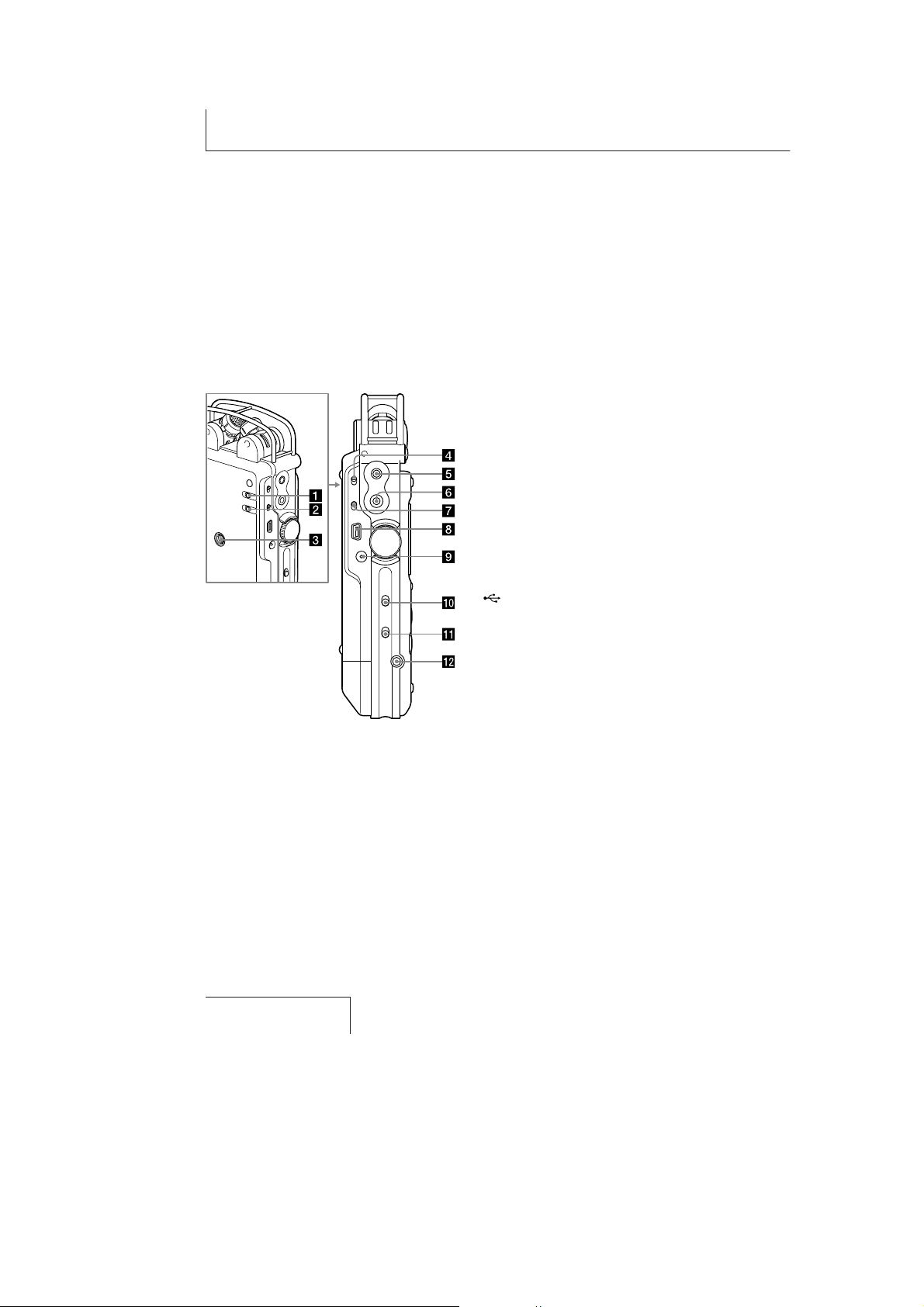
Identifying parts and controls (continued)
PCM-D50
Left side
LIMITER switch (pages 22, 43)
LOW CUT FILTER switch (pages 22, 43)
Hole for attaching the tripod (not supplied)
INPUT switch (pages 23, 28, 29, 30)
When set to “ N” (microphone), records an
audio signal input from the built-in
microphones or an external microphone that
is connected to the
When set to “LINE,” records an audio signal
output from external equipment that is
connected to the LINE IN (OPT) jack.
LINE OUT (OPT) (line output (optical)) jack
(page 34)
(headphone) jack (pages 26, 31)
J
MIC ATT (microphone attenuator) switch
(page 22)
USB connector (page 36)
DC IN 6V jack (page 19)
HOLD switch
When set to “ON,” the buttons on the
recorder are locked to prevent accidental
operation. It is recommended that you set
this switch to “ON” during recording and
playback. To unlock the controls, set it to
“OFF.”
RB
DPC (Digital Pitch Control) switch (pages
33, 42)
RT
REMOTE jack (page 30)
N
jack.
14
7
PCM-D50
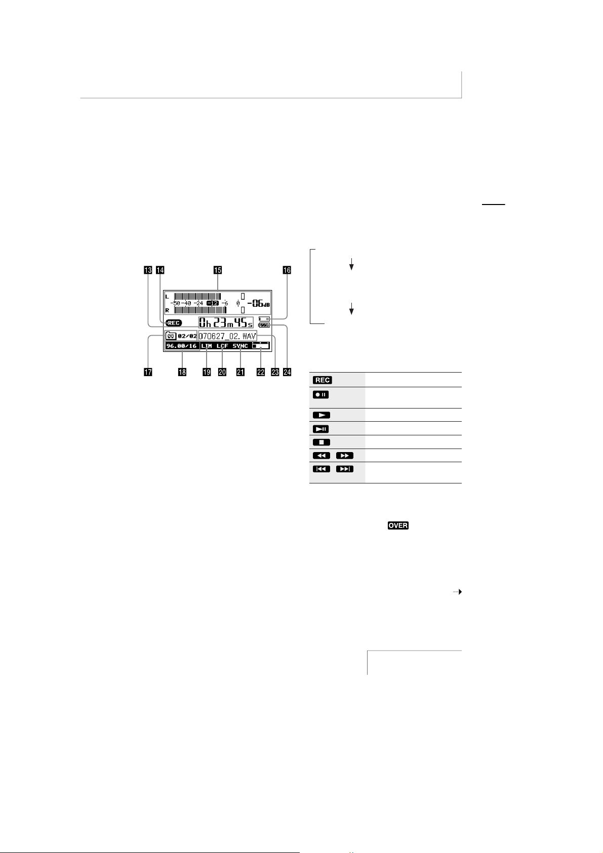
Display
RE
Time information
Each time theDISPLAY button is pressed,
the time information changes as follows
(Flashes when the recorder is paused):
/
Elapsed recording/playback time
Remaining recordable time of the
current memory (During playback:
Remaining time of the current track)
Recorded date
(During recording: Recording start date)
RG
Recording/playing status
Displays as follows according to the current
operation:
Recording
(Flashing)
(Flashing)
/
/
RH
Level meter/peak values (page 24)
Displays the level meter and the maximum
value of the peak level. When the level
exceeds the set value,
While an MP3 file is being played, displays
the artist name and title information.
Recording pause, standby for
recording
Playback
Playback pause
Stop
Fast reverse/forward
Go to previous/succeeding
tracks
appears.
Overview
Continued on the next page
15
8

Identifying parts and controls (continued)
RI
Memory Stick indicator
Displayed when the current memory is a
“Memory Stick.”
RK
Folder number, track numbers
Folders are classified into
recording and playback) and
playback only) (page 38). Track numbers are
displayed as “current track number/total
number of tracks.”
RL
Recording mode
Displays the recording mode currently
specified in the menu in the stop mode.
During playback or recording, displays the
recordin g mode of the c ur ren t t ra ck .
RM
Limiter setting
Displayed when the LIMITER switch is set to
“ON.”
X
LCF setting
Displayed when the LOW CUT FILTER switch
is set to “ON.”
XB
SYNC REC setting
Displayed when the “SYNC REC” is set to
“ON.”
XT
Remaining memory amount
Displays the remaining amount of current
memory (page 25).
XE
File information
Displays the file name of the track.
XG
Remaining battery power (page 18)
(a folder for
(a folder for
PCM-D50
16
9
PCM-D50
DISASSEMBLY
• This set can be disassembled in the order shown below.
SET
2-1. PANEL (FRONT) ASSY
(Page 11)
2-2. ORNAMENTAL BELT (UPPER) ASSY
(Page 11)
SECTION 2
2-3. BACKLIGHT BOARD
(Page 12)
2-5. REC VOL ASSY,
HP VOL ASSY
(Page 13)
2-6. DA BOARD
(Page 13)
2-7. AD BOARD,
MIC001, MIC002
(Page 14)
2-8. SYSTEM BOARD
(Page 14)
2-4. POWER BOARD
(Page 12)
10
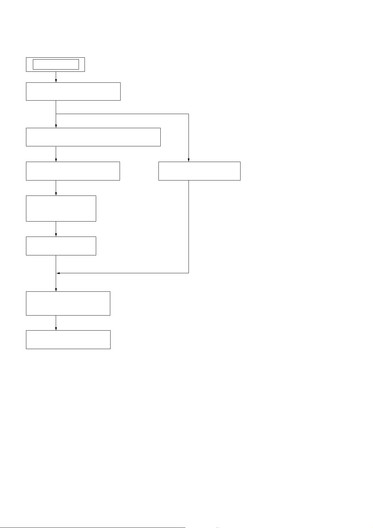
Note: Follow the disassembly procedure in the numerical order shown below.
2-1. PANEL (FRONT) ASSY
two screws
(M 1.7)
two cushions (panel)
panel (front) assy
PCM-D50
two cushions (panel)
2-2. ORNAMENTAL BELT (UPPER) ASSY
screw
(M 1.4)
ornamental belt (upper) assy
two screws
(M 1.4)
two screws
(M 1.7)
guard (MC)
screw
(M 1.4)
two cover (guard microphone)
two screws
P2 lock ace (M 1.7)
11
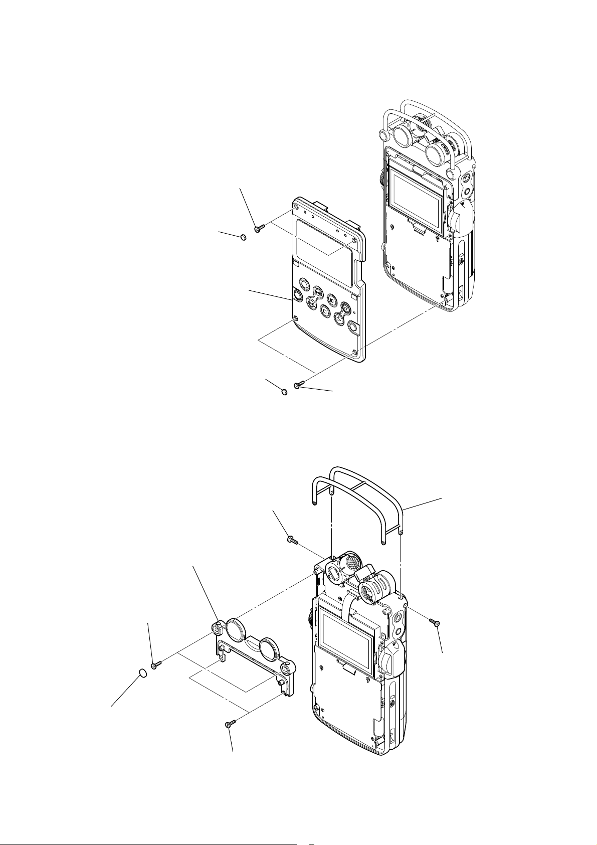
PCM-D50
2-3. BACKLIGHT BOARD
LCD assy
two screws
P2 lock ace (M 1.7)
two claws
BACKLIGHT board
LCD unit (13 core)
(CN4201)
Remove the two solders.
redwhite
LCD assy
two screws
P2 lock ace (M 1.7)
2-4. POWER BOARD
Remove the four solders.
two screws
two screws
P2 lock ace (M 1.7)
black
red
gray
white
POWER board
flexible flat cable (30core)
(CN2002)
Remove the
flexible flat cable.
12
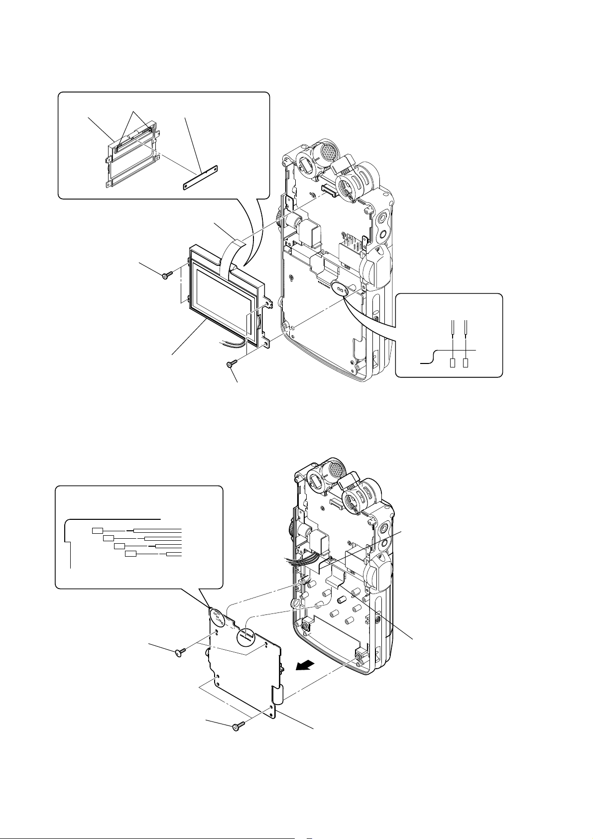
2-5. REC VOL ASSY, HP VOL ASSY
knob (VOL)
HP VOL assy
REC VOL assy
PCM-D50
Remove the six solders.
white
red
orange
yellow
gray
black
two screws
precision pan (M 1.4) (EG)
screw
2-6. DA BOARD
DA board
CN3001
two screws
(special head (M 2))
guard (VOL)
chassis (PWB)
two screws
screw
P2 lock ace (M 1.7)
13
PCM-D50
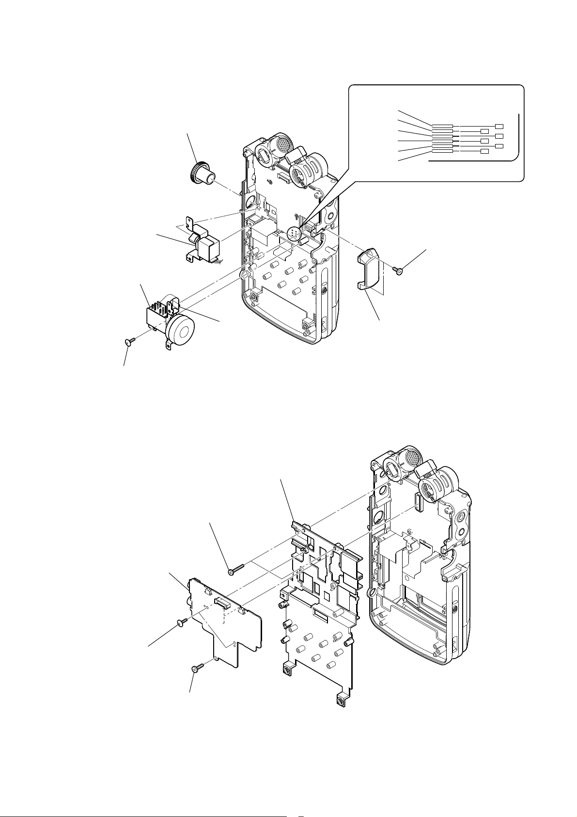
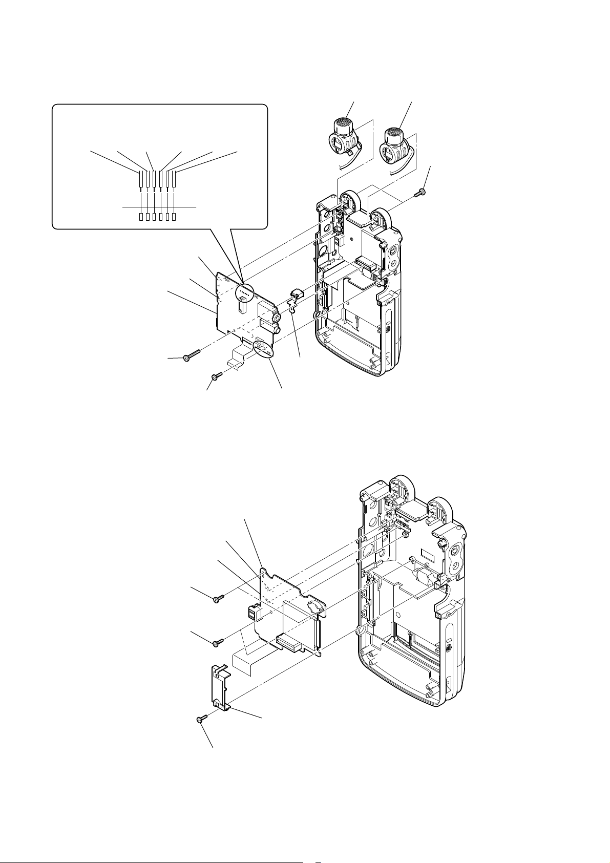
2-7. AD BOARD, MIC001, MIC002
Remove the six solders.
MIC001 MIC002
red redyellow yellowblack
S3002
S3003
AD board
MIC002 MIC001
black
two screws
P2 lock ace (M 1.7)
screw
(M2 grip)
2-8. SYSTEM BOARD
two screws
P2 lock ace (M 1.7)
two screws
P2 lock ace (M 1.7)
screw
(M 1.7)
S1601
S1602
ground plate
Remove the two solders.
SYSTEM board
14
guide (connector)
screw
P2 lock ace (M 1.7)
SECTION 3
TEST MODE
PCM-D50
This set provides the Test Mode that can be used for the following
check modes.
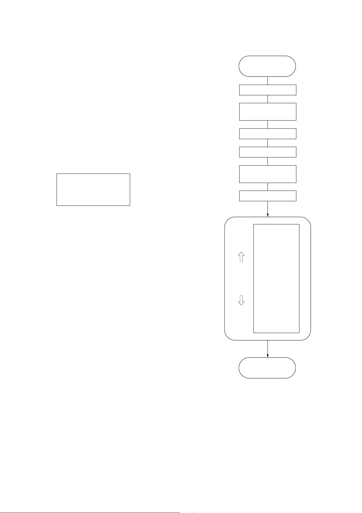
1. Setting and Exiting the TEST MODE
• Types of TEST MODE and setting the TEST MODE
1 Setting the SERVICE MODE:
(1) Turn on power to the set. Turn the LIMITER switch
on while pressing [A-B] button and [DIVIDE] button
at the same time.
• Exiting the SERVICE/TEST MODE
The TEST MODE is cancelled by turning off power (remov-
ing the battery).
(See Section 5. Flow Chart of the TEST MODE.)
2. Initial State of the TEST MODE and Exiting Method
• Initial state upon entry into the TEST MODE: “OK” is sent
to the PC through RS-232C.
Example of LCD display
Version
KeyChk+Fmt
DSP Loop
Lcd Contrast
Cluster Num
3. OK or NG Judgment
OK or NG judgment in each mode is returned by a LCD dis-
play and a status via UART.
4. How the Power of Each Section is Handled in the
TEST MODE
When TEST or SERVICE MODE is entered, the system will
keep the power state in a state equivalent to the Idle state. This
is for system to check the power device of each section for its
operation. However during execution of the Sleep command,
the system will take control based on the Sleep state since the
standby current need be measured.
5. Flow Chart of the TEST MODE
START
After power-on,
idle or sleep state
LIMITER SW OFF
Press [A-B]+[DIVIDE]
at the same time
LIMITER SW ON
Release [A-B]+[DIVIDE]
SERVICE MODE
established Menu Display
Release [A-B]+[DIVIDE]
:
Version
KeyChk+Fmt
DSP Loop
Lcd Contrast
Cluster Num
RTC Int
Battery
DCIN
VBUS
Sleep
App LogOut
Log Output
Log Clear
Menu Init
Key Check
Version
:
END
Exit from TEST MODE
6. Transitions in Each Mode
Power OFF
(Remove the battery)
15

PCM-D50
SERVICE MODE
The SERVICE MODE is entered and the details of the Service
Menu are as follows:
1 Version
Function: To check the version of the relevant module.
PCM-D50 : JP Boot : 11
ARM 1. 0. 00
DSP 1. 0. 00
Sep 18 2007 08 : 41 : 38
PCM-D50: Destination (JP, US, CN, CE)
Boot: Boot loader F/W version
ARM: F/W version for CPU (ARM section)
DSP: F/W version for CPU (DSP section)
Date: Date and time of build
2 Key Check
Function: To allow you to check inputs by pressing the cor-
responding keys.
Input checks as well as INT check. (KEY confi rmation checks
and KEY_WAKE interrupt check)
Target keys to be inputted:
STOP, PAUSE, FR, MENU/FOLDER, A-B,
LIGHT, DISPLAY, FF, DIVIDE,
PLAY, REC,
MIC/LINEIN, LIMITER, LCF, DPC, HOLD,
POWERSW, and MICLR
<KEY CHECK>
KEY : - REMAIN : 18
Display the key confirmed.
Count down the number of
the remaining keys.
When an input has been determined, the backlight is illuminated for 0.5s.
When all the inputs have been confi rmed at least once, OK is
displayed on the LCD and the LED (GREEN) is lit.
3 Key Chk+Format
Function: T
o allow you to check key inputs by pressing the cor-
responding keys.
Input checks as well as INT check. (KEY confi rmation checks
and KEY_WAKE interrupt check)
Target keys to be inputted:
STOP, PAUSE, FR, MENU/FOLDER, A-B,
LIGHT, DISPLAY, FF, DIVIDE,
PLAY, REC,
MIC/LINEIN, LIMITER, LCF, DPC, HOLD
POWERSW, and MICLR
<KEY CHECK>
KEY : - REMAIN : 18
Display the key confirmed.
Count down the number of
the remaining keys.
When an input has been determined, the backlight is illuminated for 0.5s.
When all the inputs have been confi rmed at least once, NAND
is formatted (all the issues are deleted) and the MENU settings
are defaulted. (However, LCD Contrast is held.)
When the formatting has been normally completed, the system
is restarted (rebooted).
Loop
4 DSP
Function: To perform a DSP LOOP BACK.
<DSP Loop>PLAY
Input->Output
HPMUTE : OFF LINEMUTE : OFF
LIMITER : OFF
LCF : OFF
[PLAY]: Starts Loop Back
[STOP]: Stops Loop Back
[MIC/LINEIN]: As per the set control.
[LIMITER]: As per the set control.
[LCF]: As per the set control.
[DPC]: Switches HP Mute
(OFF: Mute OFF; ON: Mute ON)
[HOLD]: Switches LINE Mute
(OFF: Mute OFF; ON: Mute ON)
Input: INTMIC, EXTMIC, LINEIN
Output: HPOUT, LINEO,
5 Lcd Contrast
Function: To adjust the contrast of the LCD.
<Lcd Contrast>
Value : 07
[FF] + [FR] -
Display the current UI value.
The default (initial value) is taken as Value=XX (XXh).
This represents 2-byte transmit data after 81h (V5 Output Voltage Set) of serial communication data to the LCD module. (UI
value: This is a value displayed in the TEST MODE.)
Initial value
UI value 00 01 02 ... 10 ... 19 20
LCD[h] 20 21 22 ... 27 ... 24 35
(Each value is provisional.)
6 Cluster Num
Function: For design. Read the cluster number from memory.
7 RTC Interrupt
Function: To perform a RTC self test.
<RTC Int>
01s
RTC Int OK
The count is displayed at every second.
8 Battery
Function: To display the current value of Battery A/D and
whether it can be detected by the 5T735 detection
register.
<Battery>
A/D : 68h
DETECT : OK
[STOP/MENU] : RET
16
PCM-D50
2
R
9 DCIN
Function: To display the current value of DCIN A/D and
whether it can be detected by the 5T735 detection
register.
<DCIN>
A/D : 84h
DETECT : OK
[STOP/MENU] : RET
0 VBUS
Function: VBUS detection check.
VBUS is checked by both the 5T735 register and the M66592
register and OK is displayed when it could be detected.
<VBUS>
DETECT (5T735) : OK
DETECT (M66592) : OK
[STOP/MENU] : RET
qa Sleep
Function: Sleep test
It is tested that the Sleep Mode can be entered.
qs App LogOut
Function: For design. Output of the application’s operation
log
qd Log Output
Function: For design. Log output.
qf Log Clear
Function: For design. Log clear.
LCD Contrast Adjustment
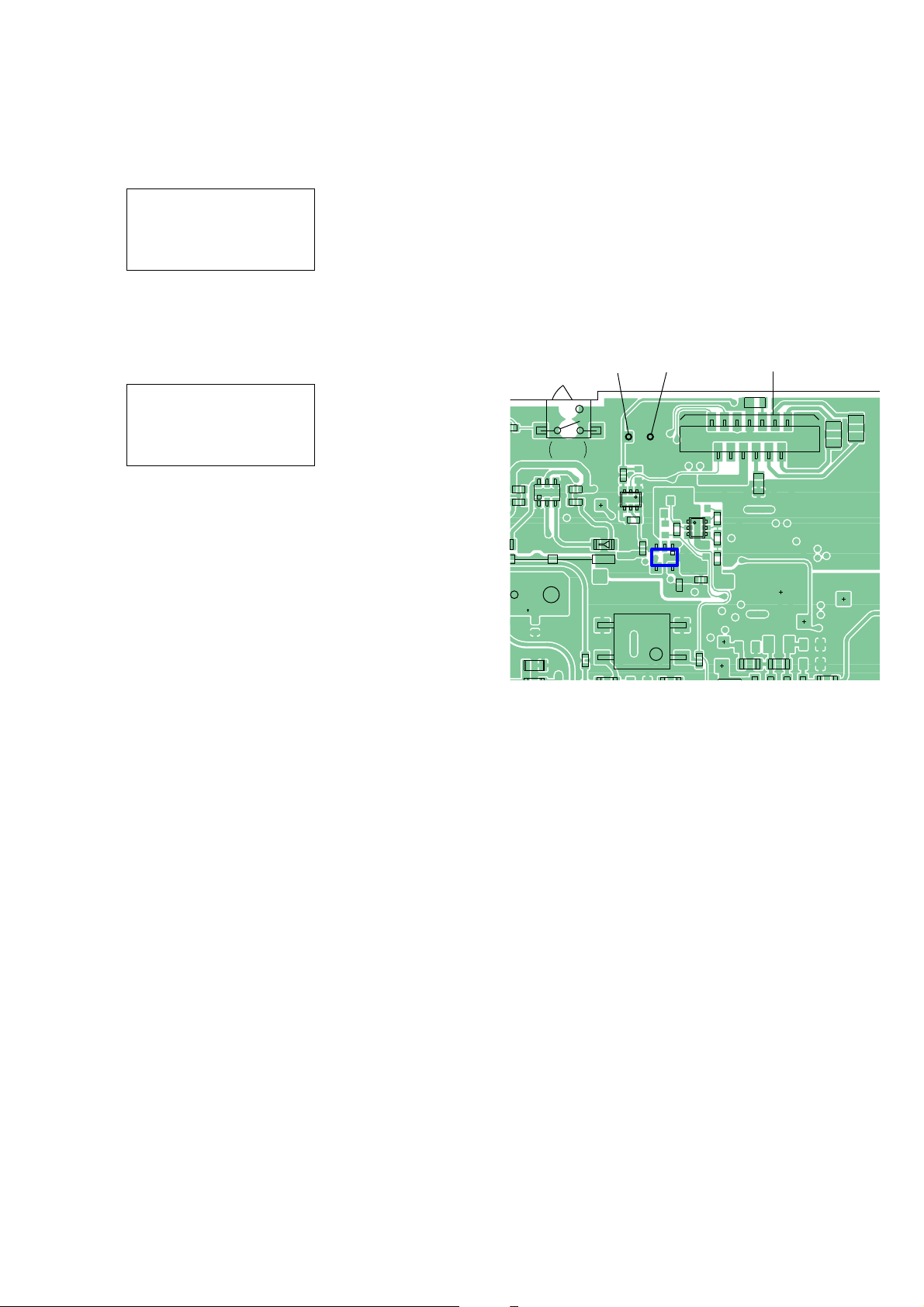
When the system board or LCD1 has been replaced, the LCD contrast should be adjusted.
1. Enter the TEST MODE and select Lcd Contrast.
2. Connect a digital voltmeter between the test points VLCD and
DGND of the DA board.
3. Use [FF] key and [FR] key to adjust the contrast until the reading on the voltmeter is 14.45±0.05V.
4. When the voltage falls within the specifi ed range, press
[PLAY] key and make sure that the display is returned to the
Menu List.
5. Exit the TEST MODE.
– DA BOARD (Side A) –
VLCD DGND
24
64
1
JL4252
402
Q4221
S4202
MIC (L-CH)
DIRECTION
3
L
R4222
R4223
R4008
JL4005
OVER
D4253
R4207
VLCD
3
Q4222
R4226
3
4
DGND
1
64
3
R4225
45
IC4007
PH4001
R4037
34
1
2
1
1
Q4032
C4065
R4024
1
6
R4092
JL4001
JL4206
R4031
R4089
R4036
C4202
CN4201
R4048
C4203
R4052
13
122
JL4201
C4250
JL4202
C4251
qg Menu Init
Function: To return the Menu settings to the factory settings.
17

PCM-D50
SECTION 4
DIAGRAMS
THIS NOTE IS COMMON FOR PRINTED WIRING BOARDS AND SCHEMATIC DIAGRAMS.
(In addition to this, the necessary note is printed in each block.)
For Printed Wiring Boards.
Note:
• X : Parts extracted from the component side.
• : Pattern from the side which enables seeing.
(The other layers' patterns are not indicated.)
Caution:
Pattern face side:
(SIDE B)
Parts face side:
(SIDE A)
• Lead layouts
Parts on the pattern face side seen from
the pattern face are indicated.
Parts on the parts face side seen from
the parts face are indicated.
CSP (Chip Size Package) Lead layout of conventional IC
surface
For Schematic Diagrams.
Note:
• All capacitors are in μF unless otherwise noted. (p: pF)
50 WV or less are not indicated except for electrolytics
and tantalums.
• All resistors are in Ω and
specifi ed.
• f : internal component.
• C : panel designation.
Note:
The components identifi ed by mark 0 or dotted
line with mark 0 are critical for safety.
Replace only with part
number specifi ed.
• A : B+ Line.
• B : B– Line.
• Power voltage is dc 6.0V and fed with regulated dc power
supply from battery terminal.
• Voltages and waveforms are dc with respect to ground
under no-signal (detuned) conditions.
no mark
[ ] : REC
• V oltages are taken with a VOM (Input impedance 10 MΩ).
Voltage variations may be noted due to normal production
• Waveforms are taken with a oscilloscope.
Voltage variations may be noted due to normal production
• Circled numbers refer to waveforms.
• Signal path.
c : REC (DIGITAL)
L : REC (ANALOG)
J : PB (DIGITAL)
F : PB (ANALOG)
• The voltage and waveform of CSP (chip size package)
: PB
: Impossible to measure
*
tolerances.
tolerances.
cannot be measured, because its lead layout is different
from that of conventional IC.
1
/4 W or less unless otherwise
Note:
Les composants identifi és
par une marque 0 sont
critiques pour la sécurité.
Ne les remplacer que par
une piéce portant le numéro spécifi é.
18
PCM-D50
PCM-D50
1919
• CIRCUITS BOARDS LOCATION
BACKLIGHT board
DA board
AD board
SYSTEM board
POWER board
• Waveforms
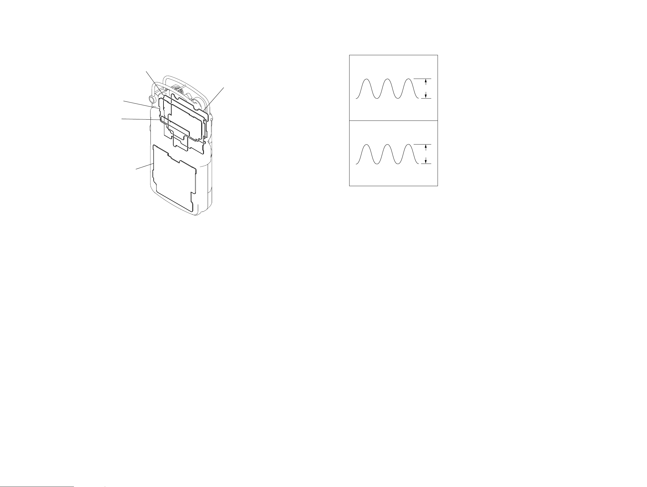
– SYSTEM Board –
IC1001 "$ (OSCOUT)
(X1401)
32.768 kHz
0.5 V/DIV, 20 μsec/DIV
IC1001 7 (CKI)
(X1101)
12 MHz
0.5 V/DIV, 50 nsec/DIV
1.3 Vp-p
2 Vp-p
PCM-D50
PCM-D50
2020
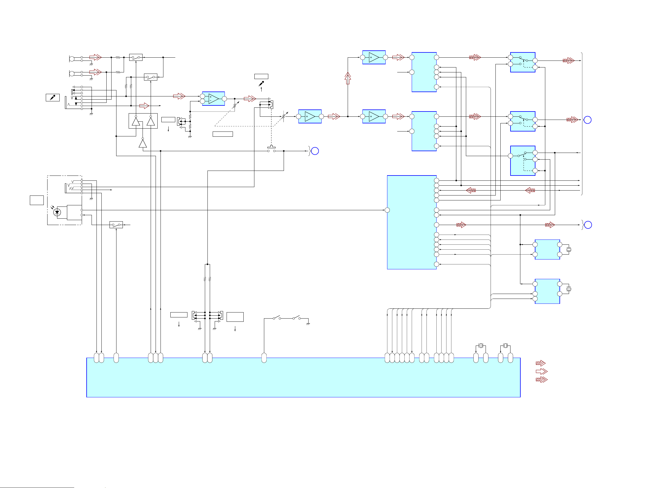
4-1. BLOCK DIAGRAM – AD Section –
3
2
1
5 7 5 7 2 6
5 7
R-CH
+D2.85VCC
DVCC_CONT
S3002 (2/2)
S3002 (1/2)
AINL
LINE AMP
IC3004
LINE AMP
IC3003
A/D CONVERTER
IC3006
DIGITAL AUDIO
I/F TRANSCEIVER
IC3404
LINE AMP
IC3002
MIC AMP
IC3001
Q3001
MIC001
(L-CH)
MIC002
(R-CH)
Q3002
Q3009
Q3008
Q3005
MIC BIAS
1
AINR
AD2_XRST
AD1_XRST
PCM0_ADDT
PCM0_BCK
PCM_MCLK
PCM0_LRCK
OPT_OUT
RX0
SDTO
12
BCK
10
LRCK
11
MCLK
R-CH
13
PDN
26
BICK
24
LRCK
28
DAUX
25
SDTO
19
UOUT
23
MCLK01
30
42
FOUT
1
CONT
4
XT1
16
TX1
36
INT0
35
OCKS0/CSN/CAD0
34
OCKS1/CCLK/SCL
33
CM1/CDTI/SDA
32
CM0/CDTO/CAD1
31
PDN
VOUT
VCC
GPI06
LINEIN_DET
OPTIN_DET
OPTIN_CONT
EXTMICBIAS_CONT
KEY_MICXLINE
EXTMIC_XDET
AB4
GPI05
AC4
CAM_CLK
AB12
CAM_YUV4
AE10
GPIO14
W2
CAM_YUV7
AB10
NAND_DA14
H12
SPI1_SI
AB8
SPI1_SO
W8
SPI1_SK
V10
SPI1_CSZ0
W10
D_TRSTZ
V19
NAND_DA12
J10
NAND_DA11
H10
NAND_DA10
H9
CAM_SCLK
AB14
CAM_STR
AB13
CAM_HS
AD12
OSCIN
AB26
OSCOUT
AC26
GPIO9
AA3
GPIO10
AA2
D_TMS
V17
S1601
LIMITER
ON
OFF
S1602
S4202
MIC (L-CH)
DIRECTION
S4201
MIC (R-CH)
DIRECTION
KEY_XLRMIC
SYSTEM CONTROL/DSP
IC1001 (1/3)
LOW CUT
FILTER
OFF
ON
S3003
MIC ATT
J3002
LINE IN
(OPT)
RV003
REC LEVEL
20
0
S3002
LINE
INPUT
2 6 3
4
6
1
AINL
A/D CONVERTER
IC3005
DATA SELECT
IC3406
DATA SELECT
IC3407
CLOCK SELECT
IC3405
CLOCK GENERATOR
IC3401
1
AINR
SDTO
12
BCK
10
LRCK
11
MCLK
R-CH
R-CH
13
PDN
3
4
6
1
3
4
6
1
DIF_INT
DIF_XCS
SPT1_CLK
SPT1_MOSI
DIF_XRST
SPT1_MISO
X11M_CONT
PCM1_ADDT
A
DA
SECTION
B
DA
SECTION
X3401
11.2896MHz
53XT
XXT
FOUT
6
CONT
1
IN1
7
CLOCK GENERATOR
IC3403
X3402
24.576MHz
32XT–
XT
X24M_CONT
DIV24M_CONT
DIF_XRST
SPT1_MISO
SPT1_MOSI
SPT1_CLK
DIF_XCS
DIF_INT
AD2_XRST
AD1_XRST
SDTO1_XAD1
DIV24M_CONT
X24M_CONT
X11M_CONT
X1401
32.768KHz
CKI
U26
CKO
T26
X1101
12MHz
E
POWER
SECTION
J3001
• R-ch is omitted due to same as L-ch.
PCM0_DADT
SDTO1_XAD1
• SIGNAL PATH
: REC (ANALOG)
: PB (DIGITAL)
: REC (DIGITAL)
(Page 22)
(Page 21)
(Page 21)
PCM-D50
PCM-D50
2121
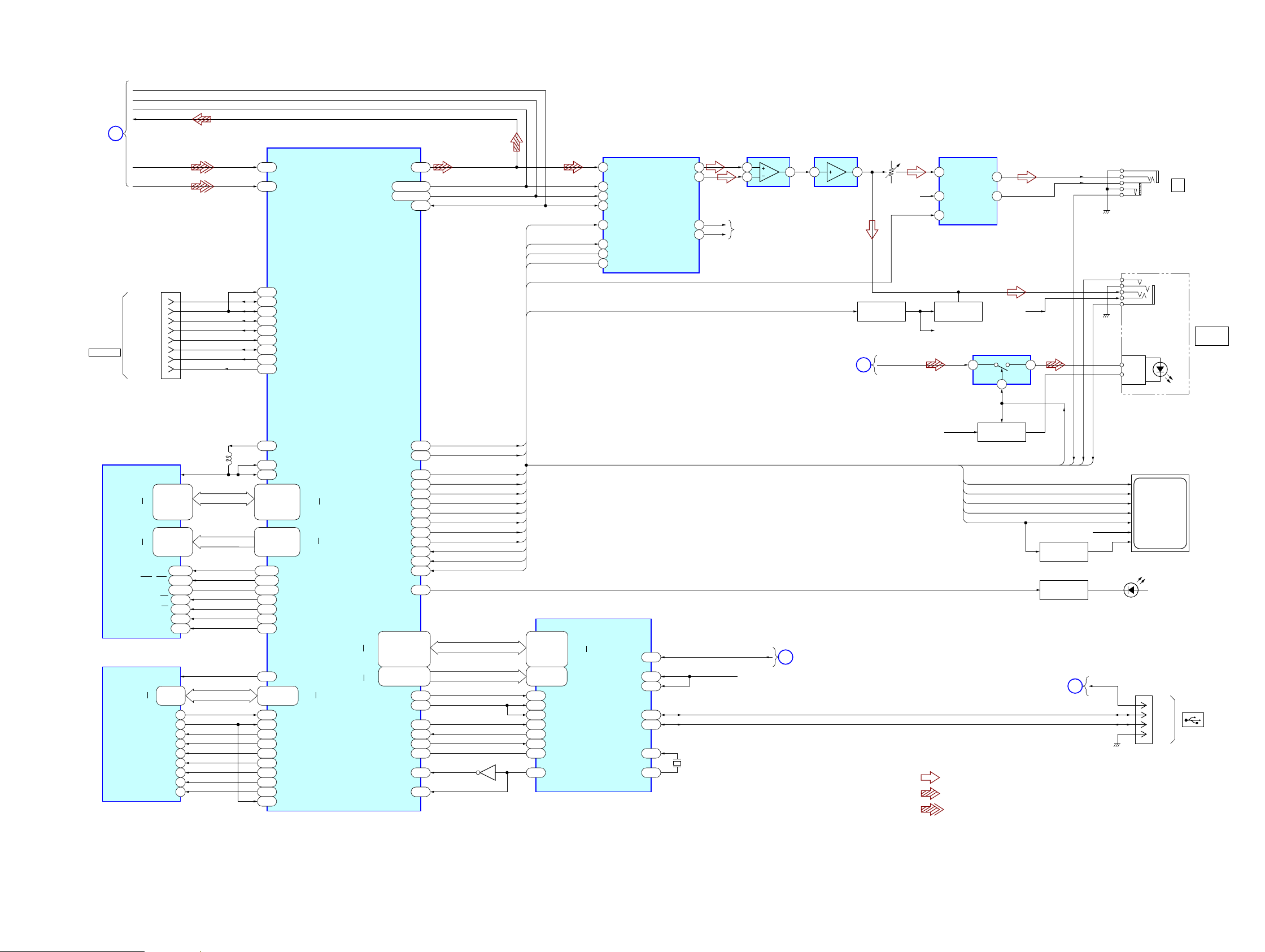
4-2. BLOCK DIAGRAM – DA Section –
H13
AB18
19
XWP
NAND_XWP
NAND_XWR
NAND_ALE
NAND_CLE
NAND_XCS1
NAND_XCS0
USB_XINT
USB_INT
USB_XRST
AB0_XDACK
AB0_XDEQ
AB0_XWR
AB0_XRD
USB_XCS
NAND_XRD
NAND_RXB0
NAND_RXB1
VDD_GP3
NAND ROM
IC1301
MS_INSZ
J5
SDR_DATA30
AB3
GPIO7
E2
XOUT
E1
XIN
B1
DM
C1
DP
G1
VIF
D7
VIF
C2
VBUS
H16
AB0_WRZ
AC23
PWM0
AD2
GPIO3
AC5
GPIO4
Y2
GPIO13
AC12
CAM_VS
U19
D_TCK
AC6
SPI0_CSZ0
W22
D_TDI
AD7
SPI0_CSZ2
AC7
SPI0_SK
AC8
SPI0_SO
H11
NAND_DA13
J9
NAND_DA9
E7
NAND_DA8
W19
EXTPCMCLK
AB22,AB20
PM0_SEN, PM1_SEN
AC21,AB21
PM0_CLK, PM1_CLK
AC22
PM0_SO
J19
AB0_RDZ
H5
SDR_DATA31
F23
AB0_A24/DAK
E24
AB0_A25/DRQ
H17
AB0_CSZ0
NAND_DA15
A4
NAND_WEZ
D3
NAND_ALE
C6
INT_N
A2
RST_N
D4
DACK0_N
DREQ0_N
A5
CS_N
B5
WR1_N
C5
WR0_N
A6
RD_N
A1–5,A6/ALE
USB I/F
IC1503
D/A CONVERTER
IC4005
SYSTEM CONTROL/DSP
IC1001 (2/3)
VDD_IOA
PSW_VCC.BUS
SPI0_MOST
+D2.85VCC
OPT_OUT
INL+
R-CH
R-CH
OPTOUT_DET
OPTOUT_CONT
LINEOUT_XDET
HP_DET
SPI0_CLK
BLCD_A0
BLCD_CS
BLCD_XRST
VDD_GP2
VLCD
VDD
VBUS
VBUS
1
3
2
5
D+
D–
GND
E9
NAND_CLE
C2
NAND_CSZ1
M9
NAND_CSZ0
E3
NAND_REZ
D2
NAND_RBZ0
H8
NAND_RBZ1
AF23
VGP3
18
XWE
17
ALE
16
CLE
10
XCE2(NC)
9
XCE1
8
XRE
7
R/B1
VCC
6
R/B2(NC.GND)
29–32,
41–44
B4,C4,D4,E4,
L9,E6,K9,E8
I/O0
I/O7
NAND_DA0
NAND_DA7
H18,H19,D18,
E18,C20,D20
AB0_A1
AB0_A6
NAND_D00–07
AB0_A1–6
AB0_D00–15
OPTOUT_DET
LINEOUT_XDET
HP_DET
OPTOUT_CONT
BLCD_XRST
BLCD_CS
BLCD_A0
DA_XCS
SPI0_CLK
SPI0_MOST
DA_XRST
LINEOUT_MUTE
CPU_EXTPMCLK
PCM0_LRCK
PCM0_BCK
PCM0_DADT
HP_XMUTE
DA_XCS
HP_XMUTE
LINEOUT_MUTE
SPI0_CLK
SPI0_MOST
DA_XRST
BLCD_LIGHT
T1
CKE
SDR_CKE0
SDR_CLK
SDR_CS0
SDR_XWR
SDR_DQM0, DQM1
SDR_XRAS, XCAS
SDR_BA0, BA1
VDD_SDR
L1402
VDD_GP4
9
8
7
6
5
4
3
2
SDRAM
IC1201
CN1603
MEMORY
STICK
PRO DUO
SDR_TKE0
AA5
SDR_CLK
T3
SDR_CSZ0
R5
F3
F2
G9
F9
SDR_WEZ
P5,R4E8,F1
F8,F7
G7,G8
SDR_DQM0,DQM1
T5,U8
SDR_RASZ,CASZ
AB5,T4
SDR_BA0,BA1
AE3
DD2VFBK
AF4
DD2VFBK2
AE22
VGP4
AC18
MS_SCK0
AB15
MS_DATA3
W3
GPIO15
AB16
MS_DATA2
AB17
MS_DATA0
AC16
MS_DATA1
AC17
MS_BS
AD24
STM_DATA
SMUTE/CSN
ACKS/CCLK
DIF0/CDTI
R-CH
PDN
MCLK
LRCK
BICK
SDTI AOUTL+
PCM1_ADDT
AD20
PM1_SI
AD22
PM0_SI
AF7–9
DD2LX1–3
CLK
CS
WE
LDQM, DQM1
RAS, CAS
BA0, BA1
VCC
VCC
CLK
DATA3
INS
DATA2
DATA0
VCC/DATA1
BS
H7,H8,J8,J7,
J3,J2,H3,H2,
H1,G3,H9,G2
AA4,Y5,Y4,W5,
W4,V5,V4,V8,
U5,U4,U3,U2
A0
A11
SDR_A0
SDR_A11
SDR_A0–11
A8,B9,B8,C9,
C8,D9,D6,E9,
E1,D2,D1,C2,
C1,B2,B1,A2
R1,R8,P4,P3,
P2,P1,P8,N8,
N5,N4,N3,N2,
N1,M8,M5,M4
DQ0
DQ15
SDR_DATA0
SDR_DATA15
D24,C25,D25,F24,
E25,F25,H25,H24,
H22,H23,J22,J23,
J24,G25,G24,G23
H2,F4,G3,H3,
E4,G4
H4,F5,E5,H5,
G5,H6,G6,H7,
G7,H8,G8,F6,
F7,F8,E6,E7
AB0_D0
AB0_D15
D0,
D1/AD1
D6/AD6,
D7–15
SDR_D0–15
PCM0_ADDT
PCM0_DADT
PCM0_BCK
PCM0_LRCK
PCM_MCLK
X1501
24MHz
Q1501
D
POWER
SECTION
C
POWER
SECTION
B
AD
SECTION
CN1501
D2601–2603
(LCD BACKLIGHT)
LCD UNIT
OPT OUT SWITCH
IC4007
HEADPHONE AMP
IC4008
LINE AMP
IC4002
RV5501
(HP VOLUME)
LOW PASS FILTER
IC4004
(USB)
LED DRIVE
Q2201
+B SWITCH
Q4030
MUTE
PH4001
MUTE DRIVE
Q4032
DISCHARGE
Q4222
LCD1
LIQUID
CRYSTAL
DISPLAY
4
21
J4002
J4001
LINE OUT
(OPT)
VIN
VCC
3 12
AOUTL–
11
5
6
7 5
AOUTR+
10
AOUTR–
9
2
4
1
5
8
7
6
A
AD
SECTION
7 15
INR+
7
OUTR
R-CH
10
OUTL
12
SHDN
16
J
• R-ch is omitted due to same as L-ch.
C4
• SIGNAL PATH
: PB (DIGITAL)
: PB (ANALOG)
: REC (DIGITAL)
(Page 20)
(Page 20)
(Page 22)
(Page 22)
PCM-D50
PCM-D50
2222
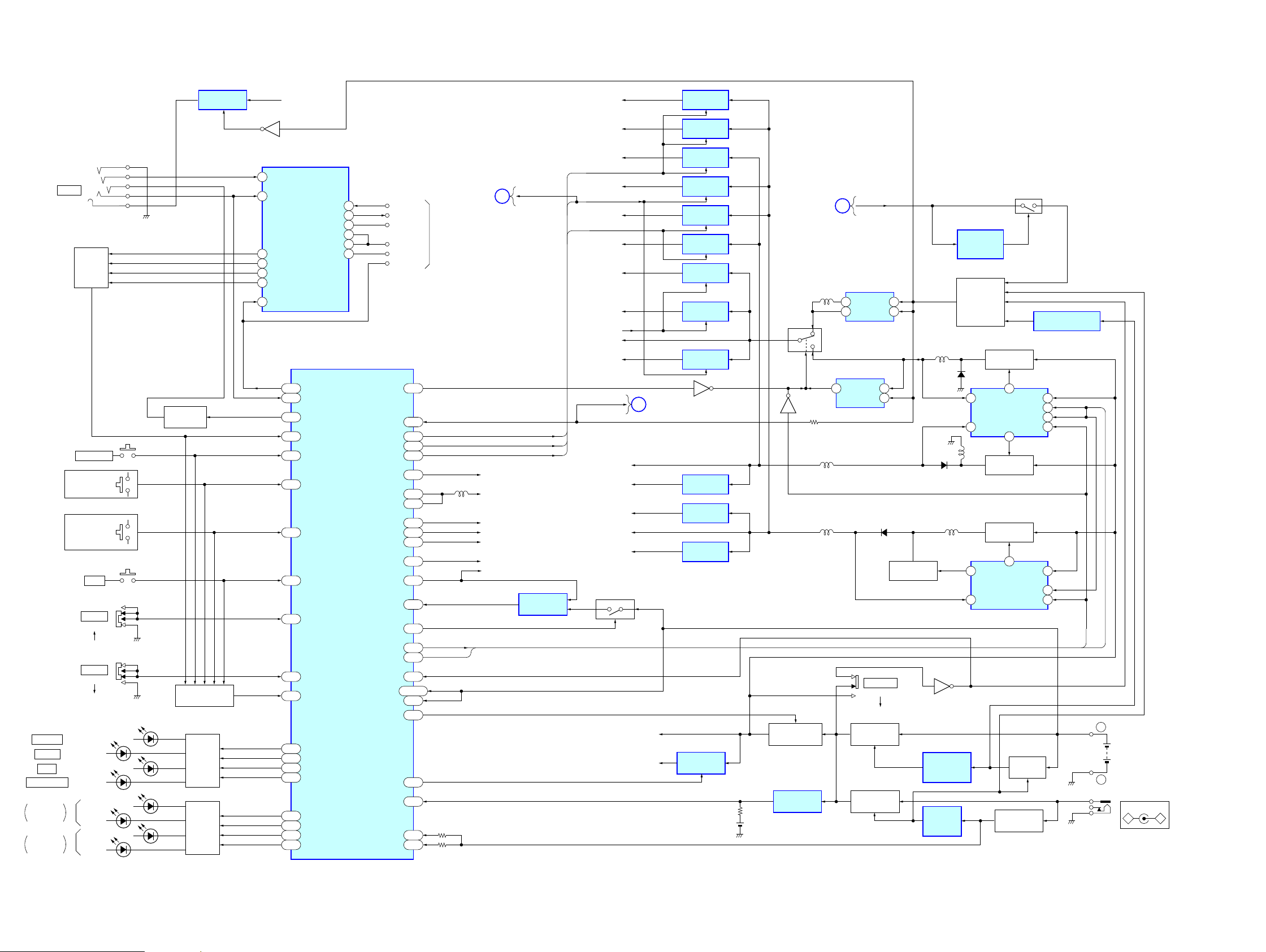
4-3. BLOCK DIAGRAM – POWER Section –
K5
B17
H4
K4
J4
LED
DRIVE
Q4220,
4221
D4250
D4251
D4252
D4253
PEAK LEVEL
(R-CH)
PEAK LEVEL
(L-CH)
PKLED_R_GRE
SDR_DATA26
SDR_DATA27
VCCADP
B6
ADIN4
AD17
BKBAT
AE11
CAM_YUV0
V18
D_TDO
AD19
IIC_SDA
AA26
VANA
C6
ADIN3
AF22
VGP2
AF20
VGP1
AC10
CAM_YUV6
Y3
GPIO12
E10
B17,D17
BATSEL
VCCVBAT1
SDR_DATA28
SDR_DATA29
SDR_DATA22
SDR_DATA24
SDR_DATA23
SDR_DATA25
GPIO0
GPIO8
GPIO1
GPIO2
PKLED_R_RED
PKLED_L_GRE
PKLED_L_RED
L2
L5
L1
H3
AD5
AB2
LED
DRIVE
Q2202,
2203
D2203
D2201
D2204
D2202
LED_GREEN
RTC_BKBAT
UNREG
POWER_ON
HP_CONT
DDC_PWM
VDD_ANA
BATT_AD
VDD_GP2
+5.3V UPDDC
-5.3V UPDDC
+5V
(IC4005)
Q1401,1402
+5V
VDD_GP1
ADA_PWM
POWERSW_OFF_DET
+3.5V
(IC4008)
LED_RED
LED_YELLOW
LED_ORANGE
KEY_XDPC
KEY_HOLD
KEY_REC
KEY_AD0
KEY_AD1
KEY_AD2
KEY_AD3
LED_ANSWER
ACCESS
PAUSE
REC
PLAY/ENTER
KEY WAKE DETECT
Q2206, 2207
AD4
AD3
ADIN5
C7
S2213
OFF
ON
DPC
S2211
OFF
ON
HOLD
S2201
REC
ADIN7
C8
SDR_DATA21
SIRCS_KEY_STOP
SIRCS_KEY_REC
SIRCS_KEY_PAUSE
SIRCS_KEY_DIVIDE
L3
ADIN8
B8
GPIO11
AA1
PWM1
nRESET
P00/TI000
P01/TI010/TO00
ANI0/P20
ANI1/P21
AD23
S2207
PLAY/ENTER
KEY NETWORK
S2202, 2206,
S2209, 2210,
S2212
NETWORK
SWITCH
Q2204,
Q2205
ADIN6
B7
KEY NETWORK
S2203–2205,
S2208
LED DRIVER
Q2301
4
3
2
1
P30/INTP2/OCD1A
RESET_OUT
FLMD0
CLK
DATA
(OCD)
RX
TX
P14/RXD6
18
22
P13/TXD6
23
P32/INTP3/OCD1B
16
P31/INTP2/OCD1A
17
P122/X2/EXCLK/OCD03
8
FLMD0
7
P120/INTP0/EXLVI
DDCOUT33
5
6
+2.9V REG.
IC2303
SIRCS CONTROL
IC2301
SYSTEM CONTROL/DSP
IC1001 (3/3)
DC-DC CONVERTER
IC2101
UNREG
ADA_PWM
ADA_PWM
DDC_PWM
DC-DC CONVERTER
IC2102
LEVEL DETECT
IC2105
+3.3V REG.
IC2103
DELAY SWITCH
Q2006
DELAY
Q2005, 2009
DC IN
DETECT
IC2003
BATTERY LEVEL
DETECT
IC2004
B+ SWITCH
Q2016, 2011
B+ SWITCH
Q2017, 2019
SWITCHING
Q2104
SWITCHING
Q2103
SWITCHING
Q2102
VBUS SWITCH
Q2008,
Q2001, 2023
SWITCHING
Q2105, 2106
B+ SWITCH
Q2030, 2020 (1/2)
+3.3V REG.
IC2001
+3.5V REG.
IC4204
+5V REG.
IC4203
+5V REG.
IC4202
-5V REG.
IC4201
+2.8V REG.
IC3209
VBUS LEVEL
DETECT
IC2002
BATT LEVEL DETECT
IC2005
LEVEL BUFFER
IC1401
DC IN 6V
J3301
DRY BATTERY
SIZE “A”
(IEC DESIGNATION LR6)
4PCS. 6V
BH1401
Li-ion
BATTERY
–
+
+
–
S2002
L2102L2104
L2105
VCC_VBUS
D2106
Q2020 (2/2)
VCC_ADP
Q2026
(2/2)
Q2026 (1/2)
Q2113,
Q2114
L2103
POWER
OFF
ON
AE4
DD2VFBSW
VDD_IOA
B9
ADVCC
VDD_ADC
U25
VPLL
AF15
DD1LX2
AF14
DD1LX1
VLO
W26
AC11
CAM_YUV2
AB11
CAM_YUV3
AD10
CAM_YUV5
A17
VCCVBUS
AC19
IIC_SCL
MIC BIAS
+MIC VCC
-MIC VCC
AD_VCC
AD+5VCC
AD-5VCC
VDD_IOP
DDCOUT33
+D2.85VCC
PSW_VCCBUS
+3.1V
(IC1503)
+1.5V
(IC1503)
MICVCC_CONT
AD5_CONT
DVCC_CONT
DVCC_CONT
VDD_PLL
VDD_L1
L1401
Q2302
VDD_L0
VBUS_SELF_PWR
PSW_VCCVBUS
MICVCC_CONT
AD5_CONT
DVCC_CONT
-5V
FB
6
CE
4
PWM
3
EXT2
8
VCC
EXT1
2
1
FB2
8
PWM2
7
EN2
6
PWM1
4
FB1
3
VOUT VIN
1 3
VSEN
4
LX VIN
5
VOUT
4
1
CE
3
VDD
EXT1
EXT2
D2102
VBUS
Q2028
L2101
L2103
D2105
2
1
10
+1.5V REG.
IC1502
-5V REG.
IC3205
+5V REG.
IC3206
+5V REG.
IC3207
-5V REG.
IC3201
+5V REG.
IC3202
+5V REG.
IC3203
+3.1V REG.
IC1501
D
DA
SECTION
E
AD
SECTION
C
DA
SECTION
J2301
SIRCS
(Page 20)
(Page 21)
(Page 21)
PCM-D50
PCM-D50
2323
1234567891011 121314
A
B
C
D
E
F
G
H
I
J
+
+
+
+
+
+
+
+
115
216
1
1
1
13
64
5
10
6
12
1324
25
36
37 48
3
5
4
1
1
4
8
5
3
64
13
64
MIC
(L-CH)
MIC001 MIC002
1
2
39
40
RED
RED
BLK
BLK
YEL
YEL
MIC
(R-CH)
AD BOARD (SIDE A)
–
+
DC IN 6V
J3301
J3002 (1/2)
LINE IN
(OPT)
11
(11)
1-875-142-
–
+
DRY BATTERY
SIZE "A"
(IEC DESIGNATION LR6)
4PCS, 6V
REC VOL
FLEXIBLE BOARD
E
POWER BOARD
C
DA BOARD
CN4202
B
IC3206
IC3404
IC3401
IC3403
IC3405
IC3406
R3418
R3419
R3225
R3422
R3423
R3424
R3231
R3425
R3232
R3428
R3436
R3437
R3438
R3439
R3440
R3441
R3446
R3448
LF001
JL3301
JL3302
CN3304
C3302
X3401
X3402
FB3402
R3303
R3320
R3321
L3401
L3402
R3136
R3139
R3140
R3145
R3147
R3152
R3153
JL3009
JL3201
JL3202
JL3203
JL3010
JL3011
JL3206
JL3012
JL3013
JL3208
JL3014
JL3019
JL3401
JL3402
JL3403
JL3210
JL3405
JL3212
JL3213
JL3407
JL3214
JL3020
JL3215
JL3216
JL3023
JL3217
JL3218
JL3024
JL3029
CN3001
JL3220
JL3030
JL3031
C3002
C3003
Q3001
C3007
Q3008
Q3009
C3202
C3401
C3405
C3406
C3407
C3408
C3217
C3028
C3410
R3001
C3029
C3411
C3412
C3413
C3414
C3416
C3417
C3030
C3418
R3009
C3031
C3419
VDR001
C3226
C3036
D3206
C3037
C3420
R3402
R3403
R3404
R3408
R3216
R341
1
R3412
R3220
R3414
R3415
C3056
C3057
R3417
JL3025
JL3026
JL3032
JL3003JL3006 JL3017 JL3001JL3008 JL3016
JL3005
JL3021
JL3004
JL3209
JL3022
R3426
R3442
R3444
R3450
R3451
JL331
1 JL3314 JL3316 JL3318
JL3310 JL3313 JL3315 JL3317
4-4. PRINTED WIRING BOARD – AD Section (1/2) –
Ref. No. Location
• Semiconductor
Location
D3206 G-6
IC3206 G-6
IC3401 H-11
IC3403 G-11
IC3404 G-9
IC3405 E-10
IC3406 E-10
Q3001 B-9
Q3008 A-9
Q3009 B-9
• : Uses unleaded solder.
• See page 19 for Circuit Boards Location.
(Page 29)
(Page 39)
(Page 30)
PCM-D50
PCM-D50
2424
4-5. PRINTED WIRING BOARD – AD Section (2/2) –
• : Uses unleaded solder.
• See page 19 for Circuit Boards Location.
1
A
B
C
D
E
F
G
H
I
J
234567891011 121314
AD BOARD (SIDE B)
J3001
J3002 (2/2)
LINE IN
(OPT)
S3002
INPUT
LINE
S3003
MIC ATT
0
20
1
2
49
50
11
(11)
1-875-142-
1
1
1
1
1
8
16
9
1
14
85
1
3
6
4
8
16
9
3
5
4
3
54
4
8
5
4
85
1
1
3
5
4
1
3
6
4
4
85
14
85
IC3001
IC3002
IC3003
IC3005
IC3006
IC3205
IC3201
IC3202
IC3203
IC3004
IC3209
IC3407
IC3207
R3224
C3058
C3059
R3226
R3229
R3036
C3060
R3038
R3039
R3230
R3040
R3041
R3043
R3044
R3045
R3047
R3048
R3051
R3052
R3055
R3056
R3057
R3058
R3059
R3060
R3066
R3069
R3071
R3072
R3073
R3074
R3075
R3090
R3091
R3092
R3093
R3094
R3095
R3096
R3097
R3098
R3099
JL3320
JL3322
JL3323
JL3324
CN3301
R3100
R3101
R3102
R3103
R3104
R3105
R3107
R3109
R3304
R3305
R3308
R3309
L3001
L3002
L3003
R3132
R3133
R3135
R3141
R3143
R3144
R3146
R3149
R3150
C3001
C3005
Q3002
Q3005
C3009
C3201
C3204
C3010
C3205
C3011
C3206
C3012
C3013
C3014
C3019
C3211
C3212
C3020
C3021
C3216
C3022
C3023
C3024
C3219
C3025
C3026
C3027
D3005
D3006
R3002
R3003
D3007
D3008
D3009
R3005
R3006
R3007
R3008
D3201
C3225
C3032
D3202
C3227
D3203
C3033
D3010
C3034
R3201
C3035
C3229
D3205
D3011
R3202
D3012
R3203
R3204
R3010
C3038
C3039
R3206
R3012
R3207
R3013
R3014
C3230
R3209
R3015
C3232
C3233
R3210
C3044
C3045
C3046
C3047
R3214
R3215
R3022
R3217
R3023
R3024
R3025
C3050
R3029
C3051
C3052
C3053
C3054
R3221
C3055
R3223
R3064
R3108
C3213
R3211
R3037
R3042
R3004
SYSTEM BOARD
CN1602
A
Ref. No. Location
• Semiconductor
Location
D3005 E-9
D3006 D-10
D3007 F-9
D3008 G-9
D3009 E-9
D3010 E-9
D3011 G-9
D3012 F-9
D3201 C-9
D3202 C-10
D3203 A-10
D3205 H-6
IC3001 C-6
IC3002 G-4
IC3003 E-5
IC3004 F-7
IC3005 E-10
IC3006 G-10
IC3201 C-10
IC3202 C-11
IC3203 B-11
IC3205 G-6
IC3207 E-8
IC3209 G-12
IC3407 H-10
Q3002 B-8
Q3005 D-4
(Page 32)
 Loading...