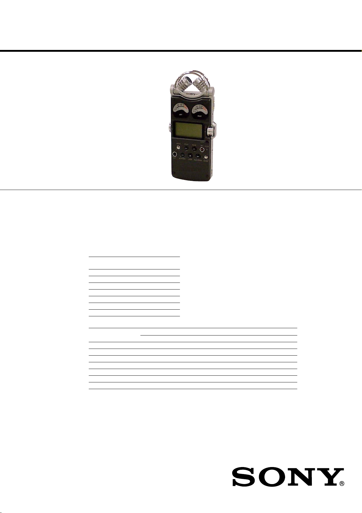
Sony PCM-D1 Service Manual
微电子时空 基准带 好音乐的休闲时光
fzmcu.taobao.com
SERVICE MANUAL
Ver. 1.0 2005.12
Recording media
PCM-D1
US Model
SPECIFICATIONS
Built-in flash memory 4 GB, “Memory Stick PRO (High Speed)”
(not supplied), Stereo recording
Maximum recordable time (Approximate)
The total maximum recordable time (approximate) of all the folders is as follows.
Built-in flash memory (4 GB)
Sampling frequency/ Maximum
quantifying bit number recordable time *
22.05 kHz 16 bit 13 hrs 10 min.
44.10 kHz 16 bit 6 hrs 35 min.
44.10 kHz 24 bit 4 hrs 20 min.
48.00 kHz 16 bit 6 hrs
48.00 kHz 24 bit 4 hrs
96.00 kHz 16 bit 3 hrs
96.00 kHz 24 bit 2 hrs
“Memory Stick PRO (High Speed)”
Sampling frequency/
quantifying bit number
22.05 kHz 16 bit 45 min. 1 hr 30 min. 3 hrs 5 min. 6 hrs 25 min. 12 hrs 45 min.
44.10 kHz 16 bit 20 min. 45 min. 1 hr 30 min. 3 hrs 10 min. 6 hrs 20 min.
44.10 kHz 24 bit 15 min. 30 min. 1 hr 2 hrs 5 min. 4 hrs 15 min.
48.00 kHz 16 bit 20 min. 40 min. 1 hr 25 min. 2 hrs 55 min. 5 hrs 50 min.
48.00 kHz 24 bit 10 min. 25 min. 55 min. 1 hr 55 min. 3 hrs 50 min.
96.00 kHz 16 bit 10 min. 20 min. 40 min. 1 hr 25 min. 2 hrs 55 min.
96.00 kHz 24 bit 5 min. 10 min. 25 min. 55 min. 1 hr 55 min.
* The maximum recordable time is varied depending on recording condition.
256 MB 512 MB 1 GB 2 GB 4 GB
Maximum recordable time *
– Continued on next page –
9-879-961-01
2005L04-1
© 2005.12
LINEAR PCM RECORDER
Sony Corporation
Connect Company
Published by Sony Engineering Corporation

PCM-D1
Quantization
16-bit linear, 24-bit linear
Frequency range (Input from the LINE IN jack
when recording/playing back) (0 to –2 dB)
Fs 22.05 kHz: 20 to 10,000 Hz
Fs 44.10 kHz: 20 to 20,000 Hz
Fs 48.00 kHz: 20 to 22,000 Hz
Fs 96.00 kHz: 20 to 44,000 Hz
Signal-to-noise ratio (S/N)
96 dB or above (1 kHz IHF-A)
(for 24 bit)
Total harmonic distortion (Input from the
LINE IN jack)
22.05 kHz 16 bit, 44.10 kHz 16/24 bit:
0.008% or below (1 kHz, 22 kHz LPF)
48.00 kHz 16/24 bit, 96.00 kHz
16/24 bit: 0.008% or below (1 kHz,
22 kHz LPF)
Wow and flutter
Below measurable limit (less than
± 0.001% W.PEAK)
Input/output
MIC jack (stereo mini jack)
Input impedance: 22kΩ
Rated input level: 2.5mV
Minimum input level: 0.7mV
i (headphone) jack (stereo mini jack)
Rated output level: 400mV
Maximum output level: 30mW +
30mW or more
Load impedance: 16Ω
LINE IN jack
Input impedance: 47kΩ
Rated input level: 2.0V
Minimum input level: 570mV
LINE OUT/optical DIGITAL OUT jack
Output impedance: 220Ω
Rated output level: 1.8V
Load impedance: 22kΩ
Output level: –21 to –15dBm
(for optical digital output)
Emission wavelength: 630 to 690 nm
(for optical digital output)
DC IN 6V jack
USB connector (Hi-speed USB, Mass
Storage Class)
Memory Stick slot
General
Power requirements
DC IN 6V (AC 120V, 60 Hz)
Four size AA (LR06) nickel metal
hydride rechargeable batteries NH-AA
(supplied)
Four size AA (LR06) alkaline batteries
(not supplied)
Power consumption
2.1W
Dimensions
Approx. 72.0 × 193.0 × 32.7 mm
(2
7/8 × 63/4 × 15/16) (w/h/d) (not
including projecting parts and
controls)
Mass 525 g (18.52 oz) (including batteries)
Supplied accessories
•Windscreen
•AC power adaptor (6V)
• USB cable
• Carrying case
For carrying the recorder and the tripod
(not supplied).
• Wrist strap
• Charging set
(Battery charger BCG-34HRE, four size AA
(LR06) nickel metal hydride rechargeable
batteries NH-AA)
• Size AA (LR06) battery case
•CD-ROM
(“DigiOnSound5”*, “DigiOnAudio2
(trial version)”*, “Driver for Windows
2000”)
* For instructions, refer to the help function
of each application.
• Operating Instructions (this book)
Optional accessories
“Memory Stick PRO (High Speed)”
MSX-1GN (1 GB), MSX-2GN (2 GB),
MSX-4GN (4 GB)
“Memory Stick PRO Duo (High Speed)”
MSX-M1GN (1 GB),
MSX-M2GN (2 GB)
Stereo headphones
MDR-V900, MDR-V700DJ
Audio connecting cable
RK-G129
Optical digital cable
POC-N120B (optical mini plug y
optical mini plug)
POC-N120AB (optical mini plug y
rectangular-shaped optical plug)
External microphone
ECM-MS957
Design and specifications are subject to change
without notice.
2

PCM-D1
Flexible Circuit Board Repairing
• Keep the temperature of the soldering iron around 270˚C during
repairing.
• Do not touch the soldering iron on the same conductor of the
circuit board (within 3 times).
• Be careful not to apply force on the conductor when soldering or
unsoldering.
Notes on Chip Component Replacement
• Never reuse a disconnected chip component.
• Notice that the minus side of a tantalum capacitor may be damaged
by heat.
UNLEADED SOLDER
•
Boards requiring use of unleaded solder are printed with the leadfree mark (LF) indicating the solder contains no lead.
(Caution: Some printed circuit boards may not come printed with
the lead free mark due to their particular size.)
: LEAD FREE MARK
Unleaded solder has the following characteristics.
• Unleaded solder melts at a temperature about 40°C higher than
ordinary solder.
Ordinary soldering irons can be used but the iron tip has to be
applied to the solder joint for a slightly longer time.
Soldering irons using a temperature regulator should be set to
about 350°C.
Caution: The printed pattern (copper foil) may peel away if the
heated tip is applied for too long, so be careful!
• Strong viscosity
Unleaded solder is more viscous (sticky, less prone to flow)
than ordinary solder so use caution not to let solder bridges
occur such as on IC pins, etc.
• Usable with ordinary solder
It is best to use only unleaded solder but unleaded solder may
also be added to ordinary solder.
SAFETY-RELATED COMPONENT WARNING!!
COMPONENTS IDENTIFIED BY MARK 0 OR DOTTED LINE
WITH MARK 0 ON THE SCHEMATIC DIAGRAMS AND IN
THE PARTS LIST ARE CRITICAL TO SAFE OPERATION.
REPLACE THESE COMPONENTS WITH SONY PARTS WHOSE
PART NUMBERS APPEAR AS SHOWN IN THIS MANUAL OR
IN SUPPLEMENTS PUBLISHED BY SONY.
3

PCM-D1
TABLE OF CONTENTS
1. GENERAL ................................................................... 5
2. DISASSEMBLY
2-1. Panel (Front) Block Assy ................................................ 10
2-2. Power Board .................................................................... 10
2-3. Meter (VU) ...................................................................... 11
2-4. VOL Block Assy.............................................................. 11
2-5. Audio (D/A) Board .......................................................... 12
2-6. Audio (A/D) Board .......................................................... 12
2-7. LCD Block Assy .............................................................. 13
2-8. Main Board ...................................................................... 13
2-9. Case (MIC-F) .................................................................. 14
2-10. MIC Block Assy .............................................................. 14
2-11. Microphone Unit (R) ....................................................... 15
2-12. Microphone Unit (L) ....................................................... 15
3. TEST MODE ............................................................... 16
4. ELECTRICAL ADJUSTMENTS .......................... 18
5. DIAGRAMS
5-1. Block Diagram – Audio A/D Section – ........................... 21
5-2. Block Diagram – Audio D/A Section – ........................... 22
5-3. Block Diagram – Power Section – .................................. 23
5-4. Printed Wiring Board – Audio A/D Section – ................. 24
5-5. Schematic Diagram – Audio A/D Section (1/2) – ........... 26
5-6. Schematic Diagram – Audio A/D Section (2/2) – ........... 27
5-7. Printed Wiring Board – Audio D/A Section – ................. 28
5-8. Printed Wiring Boards
– REC/HP VOL Flexible Section (VOL Block Assy) – .. 30
5-9. Schematic Diagram – Audio D/A Section –.................... 31
5-10. Printed Wiring Board – Main Section – .......................... 32
5-11. Schematic Diagram – Main Section (1/6) – .................... 34
5-12. Schematic Diagram – Main Section (2/6) – .................... 35
5-13. Schematic Diagram – Main Section (3/6) – .................... 36
5-14. Schematic Diagram – Main Section (4/6) – .................... 37
5-15. Schematic Diagram – Main Section (5/6) – .................... 38
5-16. Schematic Diagram – Main Section (6/6) – .................... 39
5-17. Printed Wiring Board – Power Section – ........................ 40
5-18. Schematic Diagram – Power Section – ........................... 42
6. EXPLODED VIEWS
6-1. Front Panel Section ......................................................... 47
6-2. LCD Section .................................................................... 48
6-3. VOL Section .................................................................... 49
6-4. Audio (A/D) Board, Audio (D/A) Board Section............ 50
6-5. Main Board Section ......................................................... 51
6-6. MIC Section .................................................................... 52
6-7. Rear Panel Section ........................................................... 53
7. ELECTRICAL PARTS LIST .................................. 54
4
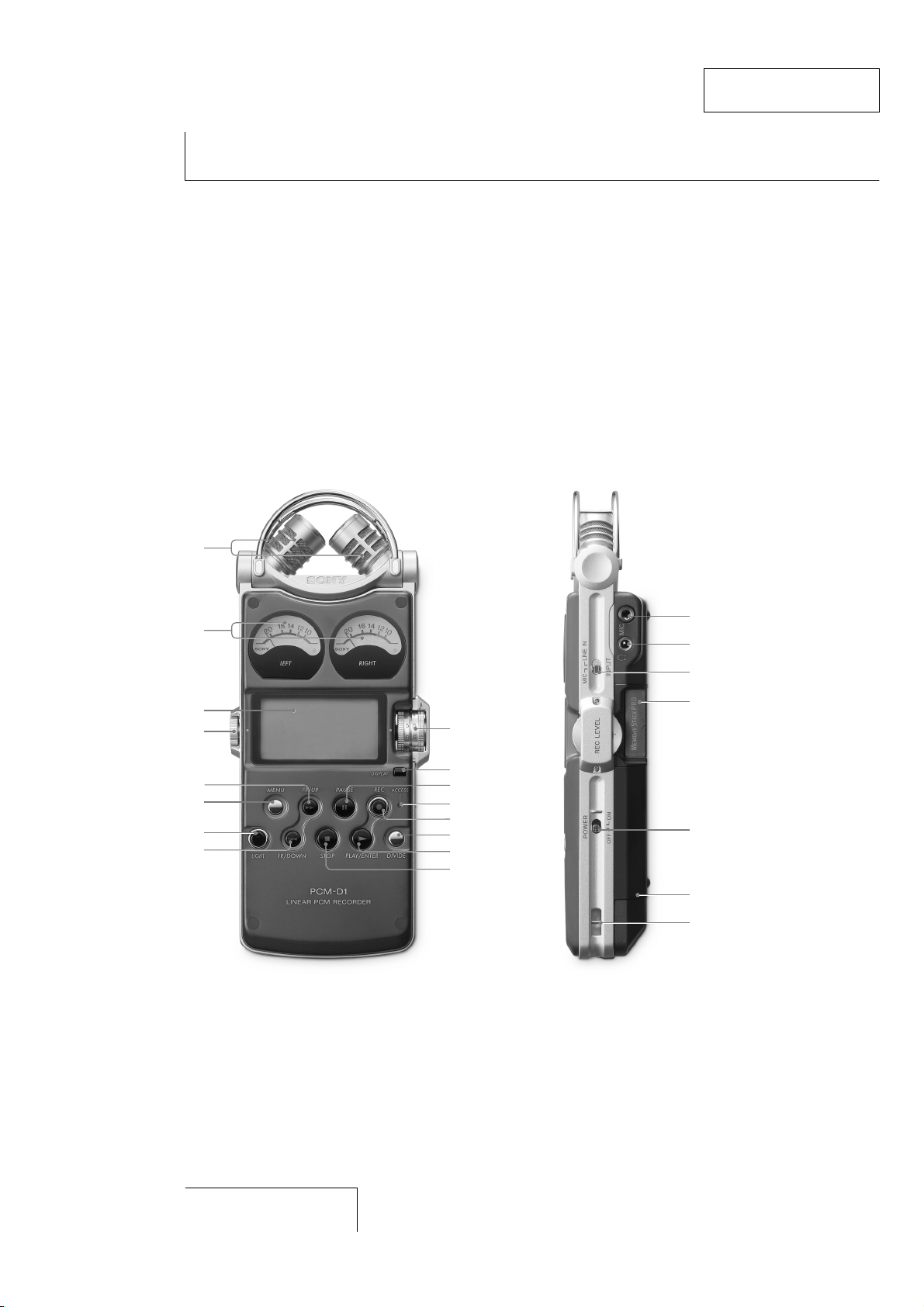
Overview (continued)
Identifying parts and controls
SECTION 1
GENERAL
PCM-D1
This section is extracted
from instruction manual.
Front
1
2
3
4
5
6
7
8
9
0
qa
qs
qd
qf
qg
qh
Right side
qj
qk
ql
w;
wa
ws
14
wd
5

PCM-D1
1
Built-in microphones (page 22)
2
Analog level meters (page 25)
Displays left and right volume levels of an
audio signal input from microphones in
analog values.
3
Display (page 16)
4
VOLUME dial
Adjusts the playback volume when turned in
+/– directions.
5
> FF (fast-forward) /UP button
(pages 21, 29)
6
MENU button (page 34)
7
LIGHT button
Turns on or off the backlight of the display
and the analog level meters.
8
. FR (fast-rewind) /DOWN button
(pages 21, 29)
9
REC LEVEL L/R (recording level left/right)
dials (page 24)
0
DISPLAY button (page 17)
Switches time information in the display.
qa
X PAUSE button/indicator (pages 25, 29)
qs
ACCESS indicator (pages 20, 38)
Flashes when accessing memory (except
during recording).
qd
z REC (recording) button/indicator
(page 24)
qf
DIVIDE button (page 30)
qg
N PLAY/ENTER button/indicator
(pages 21, 28)
qh
x STOP button (pages 25, 29)
qj
MIC (microphone) jack (page 27)
qk
i (headphone) jack (pages 26, 28)
ql
MIC (microphone) /LINE IN switch
(page 24)
When set to “MIC,” records an audio signal
input from the built-in microphones or an
external microphone that is connected to the
MIC jack. When set to “LINE IN,” records an
audio signal output from external equipment
that is connected to the LINE IN jack.
w;
Memory Stick slot (page 38)
wa
POWER switch
Turns on or off the power.
ws
Battery compartment lid (page 19)
wd
Slit for a wrist strap (page 18)
Continued on the next page
Overview
15
6
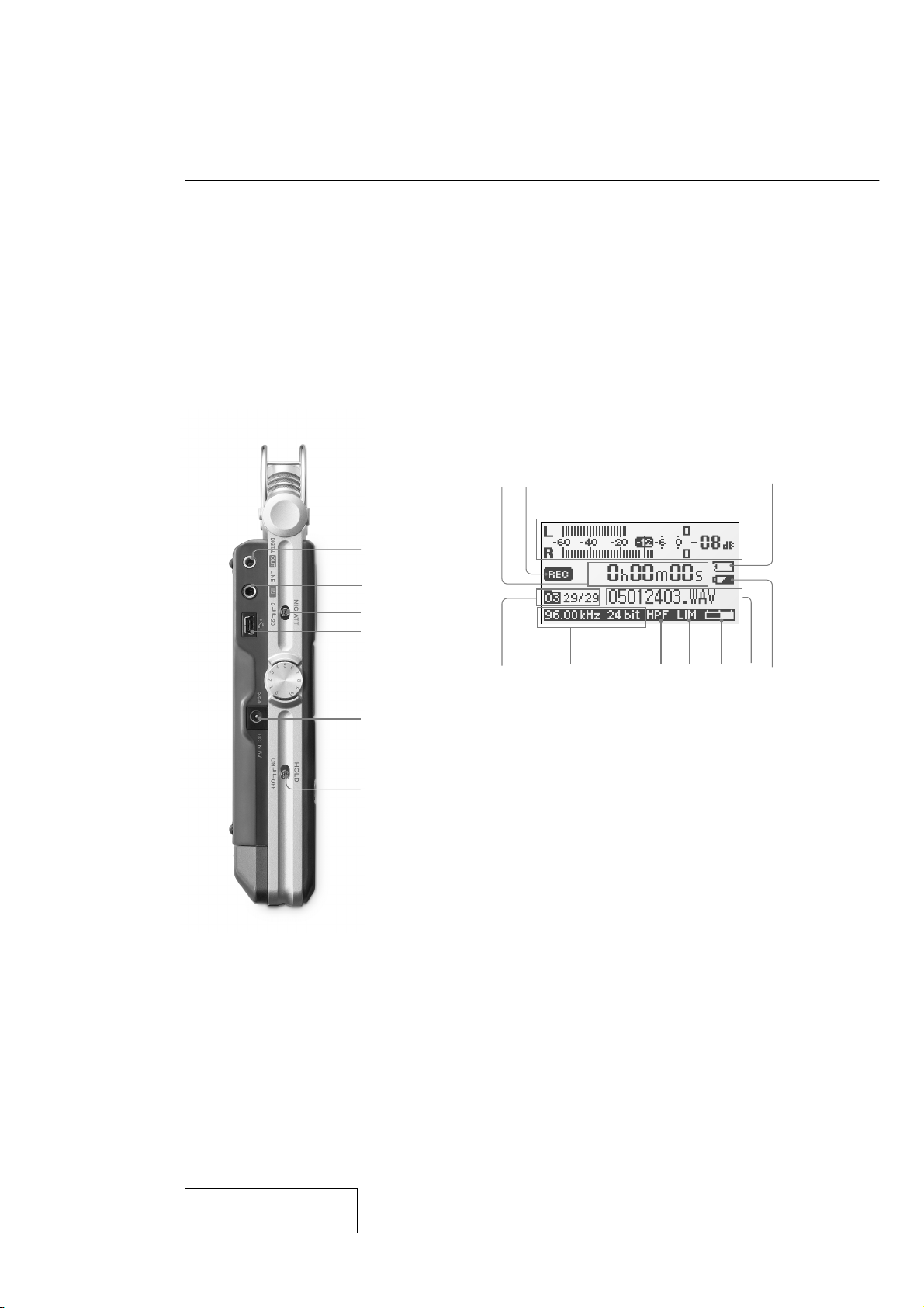
Overview (continued)
PCM-D1
Left side
1
2
3
4
5
6
Display
7
8
qa
qs
9
qd
qf
qg
0
qjqh
16
7
PCM-D1
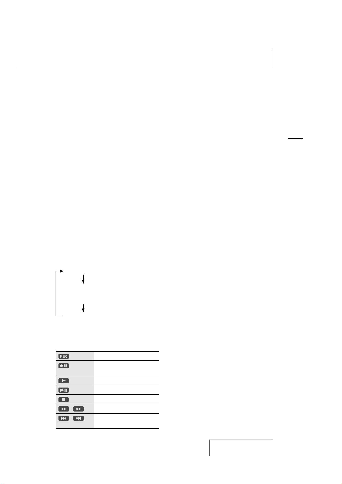
1
LINE OUT/optical DIGITAL OUT jack
(page 29)
2
LINE IN jack (page 27)
3
MIC ATT (microphone attenuator) switch
(page 23)
4
USB connector (page 30)
5
DC IN 6V jack (page 20)
6
HOLD switch
When set to “ON,” the buttons on the
recorder are locked to prevent accidental
operation. It is recommended to set to “ON”
during recording and playback. To unlock
the controls, set to “OFF.”
7
Time information
Each time the DISPLAY button is pressed,
the time information changes as follows
(Flashes when the recorder is paused):
Elapsed recording/playback time
Remaining recordable time of the current
memory (During playback: Remaining
time of the current track)
9
Peak meter (page 25)
0
Memory Stick indicator
Displayed when the current memory is a
“Memory Stick PRO (High Speed).”
qa
Folder number, track numbers
Track numbers are displayed as “current
track number/total numbers of tracks.”
qs
Sampling frequency and quantifying bit
number of currently recording/playing
track (page 35)
qd
HPF (High Pass Filter) setting
Displayed when “200Hz HPF” is set to “ON”
(page 36).
qf
Limiter setting
Displayed when “LIMITER” is set to “ON”
(page 35).
qg
Remaining memory volume
Displayed the remainig volume of current
memory (page 26).
qh
File name of currently recording/playing
track
qj
Remaining battery power (page 20)
Overview
Recorded date
(During recording: Recording start date)
8
Recording/playing status
Displays as follows according to the current
operation:
Recording
(Flashing)
(Flashing)
/
/
Recording pause,
standby for recording
Playback
Playback pause
Stop
Fast reverse/forward
Go to previous/succeeding
tracks
17
8
SECTION 2
DISASSEMBLY
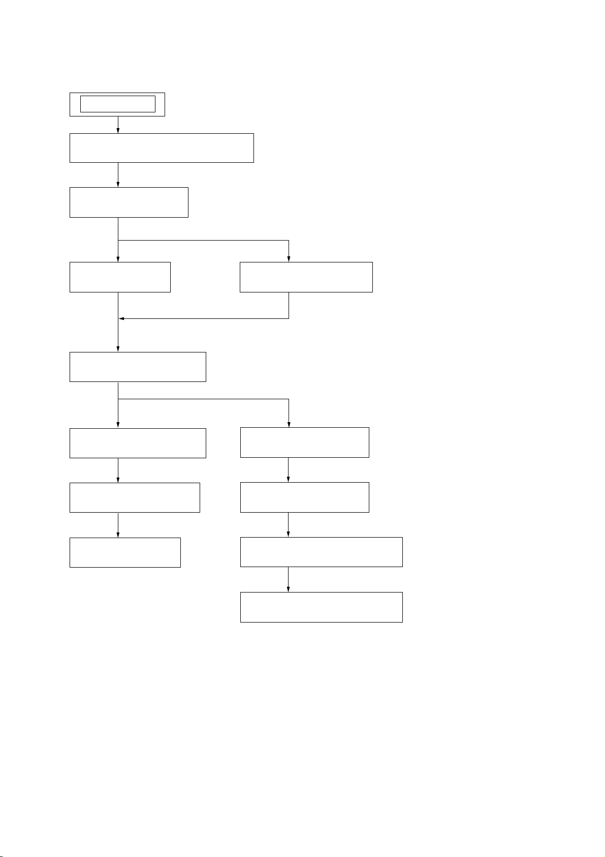
Note: This set can be disassemble according to the following sequence.
SET
2-1. PANEL (FRONT) BLOCK ASSY
(Page 10)
2-2. POWER BOARD
(Page 10)
PCM-D1
2-3. METER (VU)
(Page 11)
2-5. AUDIO (D/A) BOARD
(Page 12)
2-6. AUDIO (A/D) BOARD
(Page 12)
2-7. LCD BLOCK ASSY
(Page 13)
2-8. MAIN BOARD
(Page 13)
2-4. VOL BLOCK ASSY
(Page 11)
2-9. CASE (MIC-F)
(Page 14)
2-10. MIC BLOCK ASSY
(Page 14)
2-11. MICROPHONE UNIT (R)
(Page 15)
2-12. MICROPHONE UNIT (L)
(Page 15)
9
PCM-D1
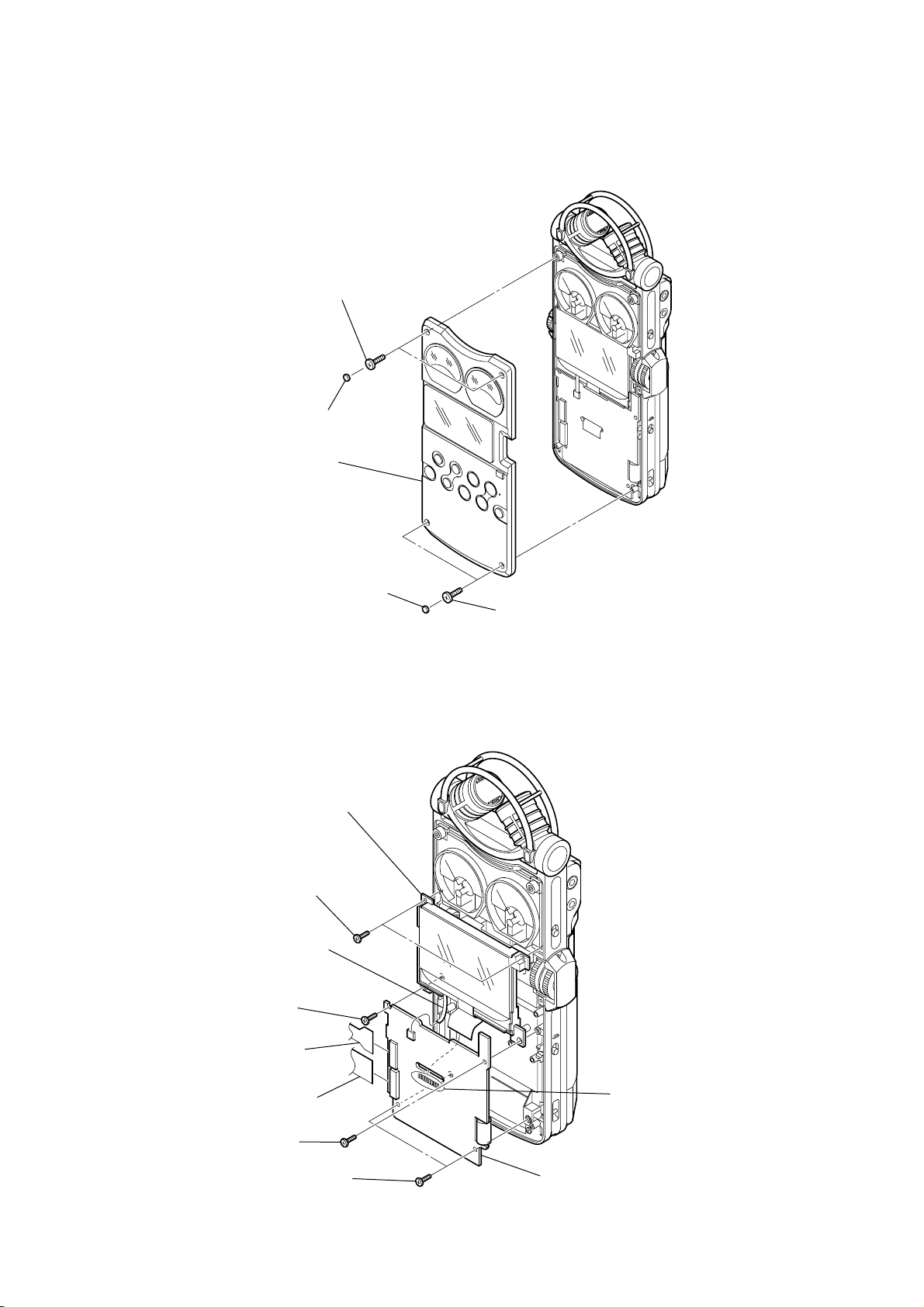
Note: Follow the disassembly procedure in the numerical order given.
2-1. PANEL (FRONT) BLOCK ASSY
3
two
screws
(M1.7)
1
two cushions (panel)
5
panel (front) block assy
2-2. POWER BOARD
1
LCD back light unit (5 core)
(CN1503)
2
two cushions (panel)
0
9
two
screws
(P2 (M1.7))
7
screw
(P2 (M1.7))
LCD block assy
4
two
screws
(M1.7)
10
3
SIG FLEXIBLE board (24 core)
(CN1502)
2
POWER FLEXIBLE board (20 core)
(CN1501)
6
screw
(P2 (M1.7))
5
(P2 (M1.7))
two
screws
8
POWER board
4
Remove the ten solders.
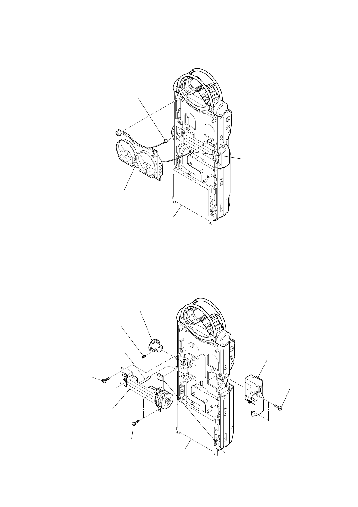
2-3. METER (VU)
y
1
CN2511
2
CN2521
PCM-D1
2-4. VOL BLOCK ASSY
3
set-SCT
(flat point HEX. 2.6
5
HP VOL FLEXIBLE board (8 core)
(CN2307)
3
meter (VU)
×
3)
4
knob (VOL)
LCD block assy
2
ornament (MS) block ass
8
two
screws
(P2 (M1.7))
9
VOL block assy
7
two
screws
(P2 (M1.7))
LCD block assy
1
two
(M1.4)
6
REC VOL FLEXIBLE board (16 core)
(CN2301)
screws
11
PCM-D1
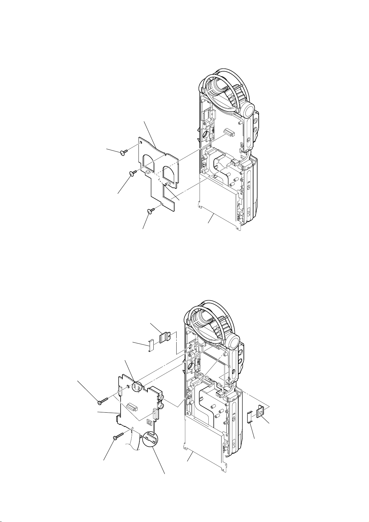
2-5. AUDIO (D/A) BOARD
2
screw
4
AUDIO (D/A) board
2-6. AUDIO (A/D) BOARD
5
Remove the six solderings.
7
two screws
(M2 grip)
1
special head screw
(M1.7)
2
1
guide (knob)
3
screw
knob (MIC ATT)
CN2201
LCD block assy
12
9
AUDIO (A/D) board
8
screw
(M2 grip)
LCD block assy
6
Remove the two solders.
4
3
guide (knob)
knob (line)
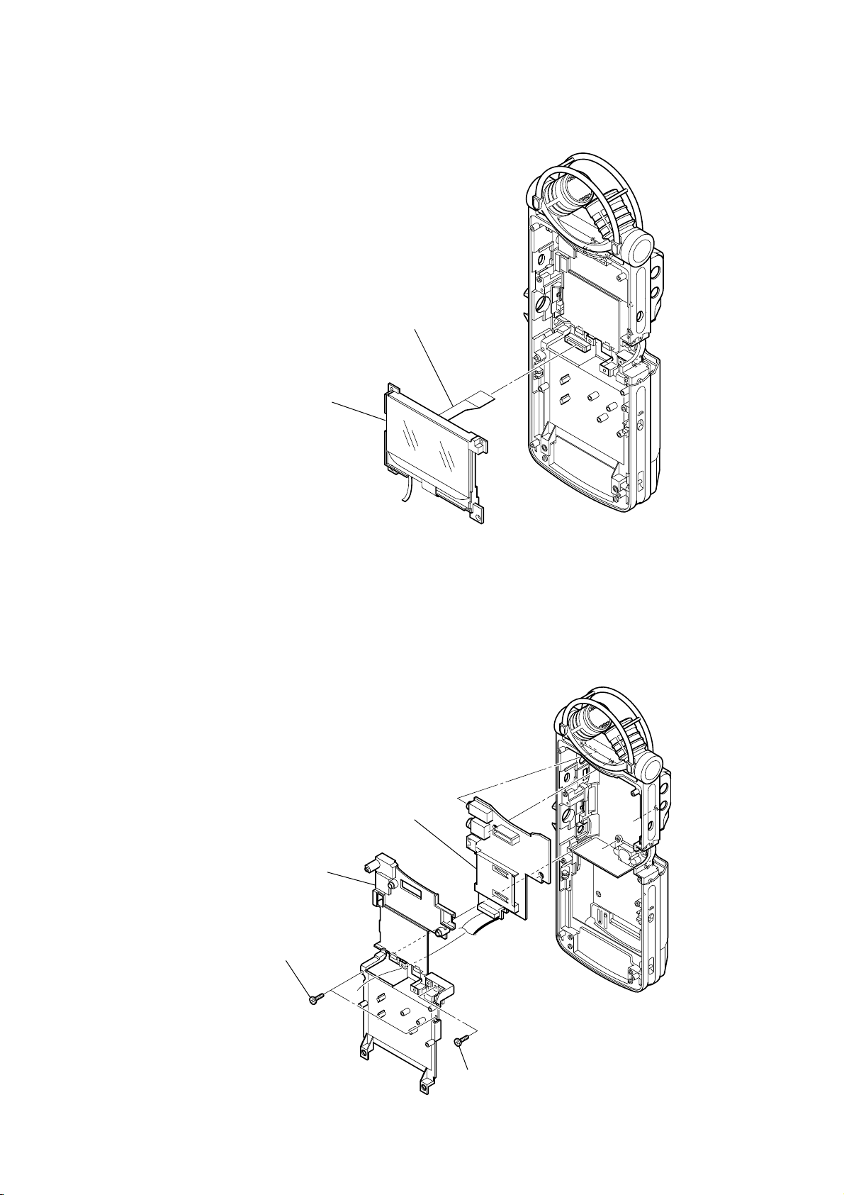
2-7. LCD BLOCK ASSY
2
LCD block assy
1
LCD unit (20 core)
(CN4151)
PCM-D1
2-8. MAIN BOARD
3
chassis
1
two
screws
(P2 (M1.7))
4
MAIN board
2
screw
(P2 (M1.7))
13
PCM-D1
s
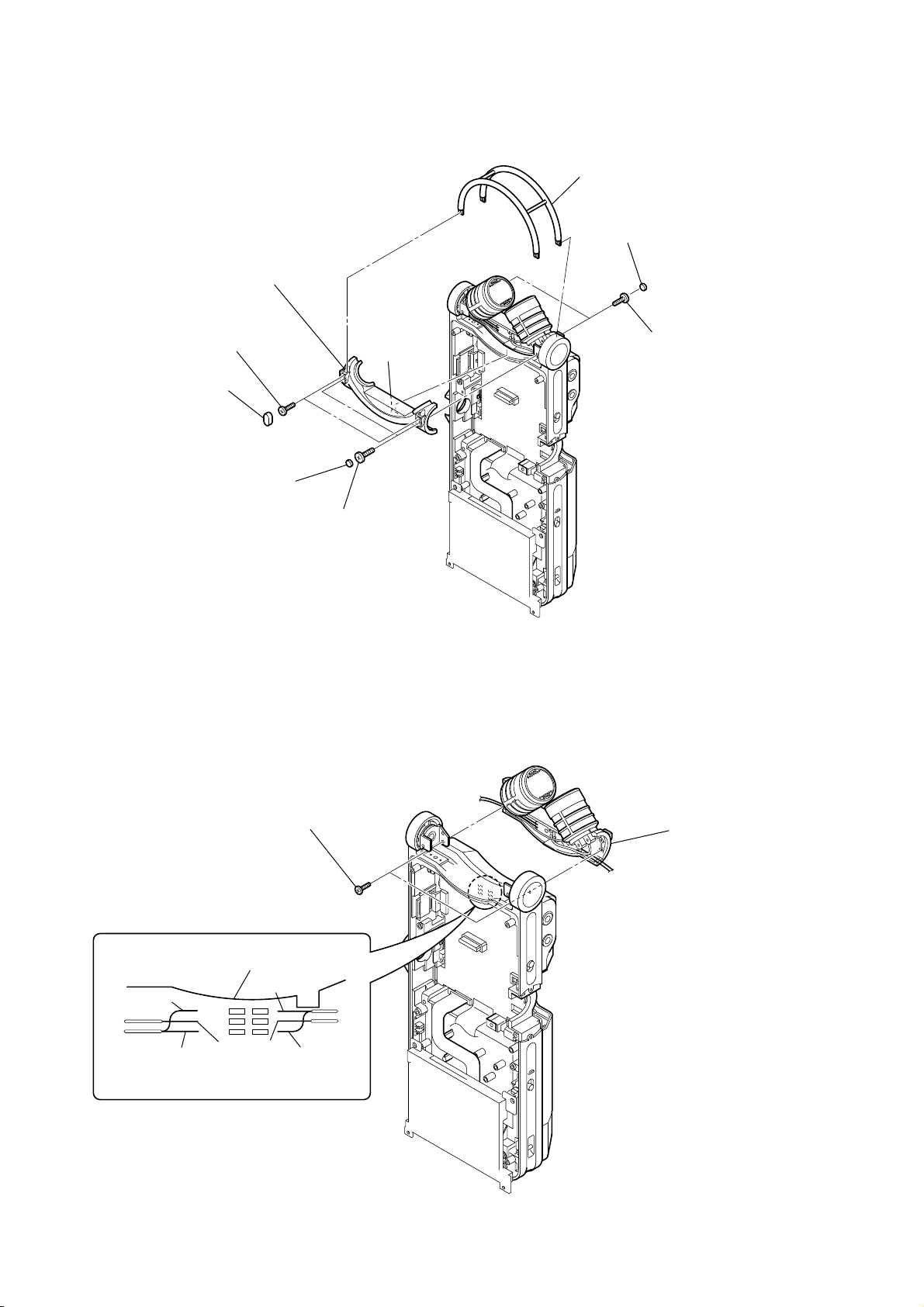
2-9. CASE (MIC-F)
1
two
(MIC-F)
8
2
two
(M1.4)
cushions
6
(MIC-F)
case (MIC-F)
screws
two
spacers
claw
7
two
screws
(M1.7)
5
guard (MIC)
3
(MIC-R)
two
cushions
4
(M1.4)
two
screw
2-10. MIC BLOCK ASSY
2
two
screws
(0 plate +P2 main EG grip M1.7)
1
Remove the six solders.
blue
orange
MAIN board
silver
blue
silver
orange
3
MIC block assy
14
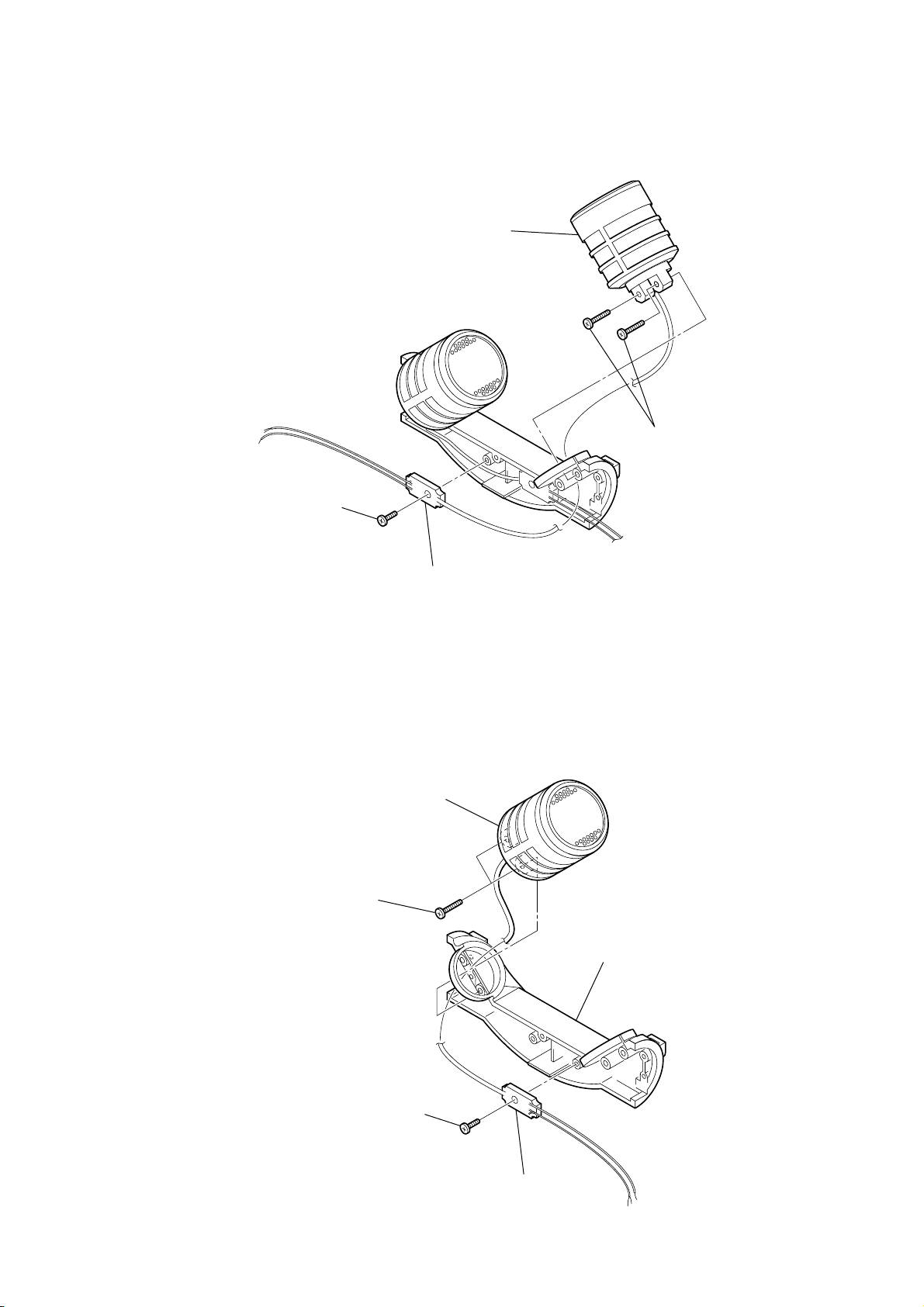
2-11. MICROPHONE UNIT (R)
1
screw
(M1.4)
2
AMP board
5
case (MIC-R)
3
two
screws
(M1.4)
4
microphone unit (R)
4
microphone unit (R)
3
two
screws
(M1.4)
PCM-D1
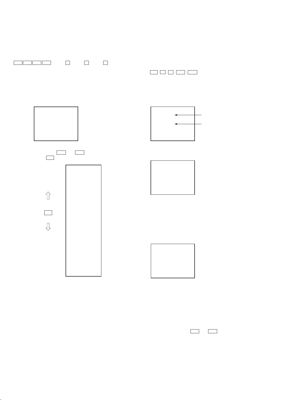
2-12. MICROPHONE UNIT (L)
1
screw
(M1.4)
2
AMP board
15
PCM-D1
SECTION 3
TEST MODE
This set provides the Test Mode that can be used for the following
check modes.
Setting the Test Mode
With the power on, press the following buttons:
> > . . [LIGHT] x [LIGHT] x [MENU] x
Canceling the Test Mode
Turn the [POWER] switch “OFF”, or remove the battery.
Test Mode Menu
When the Test Mode is entered, the following menu appears on the
LCD:
Version
F/W Update
Keychk+Fmat
Lcd Contrast
Lcd Check
Language
Loop Back
Select an item using the > and . keys, and determine its
selection using the u key.
:
Key Check
Version
F/W Update
.
Determine
using u key
>
KeyChk+Fmat
Lcd Contrast
Lcd Check
Language
Loop Back
RTC Int
System
Battery
DC-IN
VBUS
Sleep
Log Output
Log Clear
Initialize
Nand init
Nand Format
Dsp, Adjust
Reboot
:
:
1. Key Check
A specific key is inputted by pressing it for input check and INT
check.
(It is verified that input of a key is confirmed and that KEY_XWAKE
interrupt occurs)
Key to be inputted:
[REC]/ N / X / x / > / . /[MENU] / [LIGHT]/ [DIVIDE ] /
[DISPLAY]/ [HOLD] ON/OFF
Total of 11 locations
When a key is inputted and its input is confirmed, the backlight
turns on for 0.5 sec.
LCD display
<KEY CHECK>
KEY:- -
REMAIN:11
Once all key checks are completed,
OK appears on the LCD and
the LCD (ACCESS) is turned on.
<KEY CHECK>
KEY:- -
OK
Displays an input
confirmed key.
All eleven (11) keys
are counted.
2. Key Chk + Fmat Test
•When all inputs have been confirmed in Item 1, Key Check, the
system performs NAND formatting (deletion of all conditions)
and takes defaults for settings in the menu (language setting and
LCD contrast are held).
<KeyChk+Fmat>
Exec Comp
NAND formatting
(deletion of all conditions)
and default menu settings
are completed.
16
3. DSP Adjust
•This mode executes DSP LOOP BACK.
4. Lcd Contrast
• This mode adjusts the LCD contrast.
The initial value is 40.
• Adjust the contrast using the > and . keys.

PCM-D1
5. Lcd Check
•This mode verifies that all LCD indicators are on and off, and it
checks the PATTERN, vertical scroll and horizontal scroll displays.
[PLAY]: All On > : Vertical scroll
[REC]: All Off
[DIVIDE]: PATTERN
. : Horizontal scroll
x : Exit
6. Language
• Not used.
7. Loop Back
•This mode executes DSP LOOP BACK.
• MENU is turned on and off.
[PLAY]: Execute (only at a stop).
[DIVIDE]: MUTE ON/OFF.
[MENU]: Exit from Submenu.
(After an execution is stopped during execution.)
x : During execution: Termination of execution.
At a stop: Exit from submenu.
8. RTC Int
•This mode checks for RTC operation.
9. System
•This mode checks the NOR, NAND, UNIQUE and MS.
10. Battery
•This mode checks the current value of A/D.
11. DC-IN
•This mode checks the current value of DC-IN A/D.
• NG is displayed for non-connection.
12. Initialize
•This mode initializes the set values (to the values established at
the factory).
13. Nand init
• Band Block and NAND formatting of the NAND FLASH.
14. Nand Format
•NAND formatting.
15. F/W update
• Update of the F/W.
15-1. F/W UpGrade method
If the F/W need be updated for reasons such as modification of
bugs after mass production, the F/W should be updated as follows:
1. Copy the following files just under the drive of the memory stick
Duo.
(The files below will be distributed when bugs are modified.)
• ldrasm.mot (upgrade driver)
• CHIPEXEC.MOT (F/W for the set)
• update.pls (upgrade MS identification file)
2. Insert the MS described in step 1 into the set and turn on power.
(Use a new battery or the AC adapter.)
3. When the ACCESS screen remains as it is and the OPE-LED
(red) lights up, the update is completed.
Remove the battery and remove the MS Duo. The F/W update is
complete.
Enter the Test Mode and check the version.
4. Once the F/W is updated, the update.pls file is automatically
deleted.
If you are repeating to upgrade the F/W, the update.pls file should
be copied again.
Supplement:
If you are upgrading a large number of sets for mass production,
the testmode.ind file should be added which enables repeated
upgrade.
• ldrasm.mot (upgrade driver)
• CHIPEXEC.MOT (F/W for the set)
• update.pls (upgrade MS identification file)
• testmode.ind (special file for the factory)
Caution:
If the power is down during upgrade or the memory stick is removed,
this upgrade fails.
(This will cause malfunctions, failure of power-on, and errors during
operation.)
If these conditions are caused, the set must be disassembled and
upgraded. Contact the design department.
The following files can be created by creating an arbitrary text file
and changing its name.
• update.pls (upgrade MS identification file)
• testmode.ind (special file for the factory)
17
PCM-D1
SECTION 4
ELECTRICAL ADJUSTMENT
Level Meter Adjustment
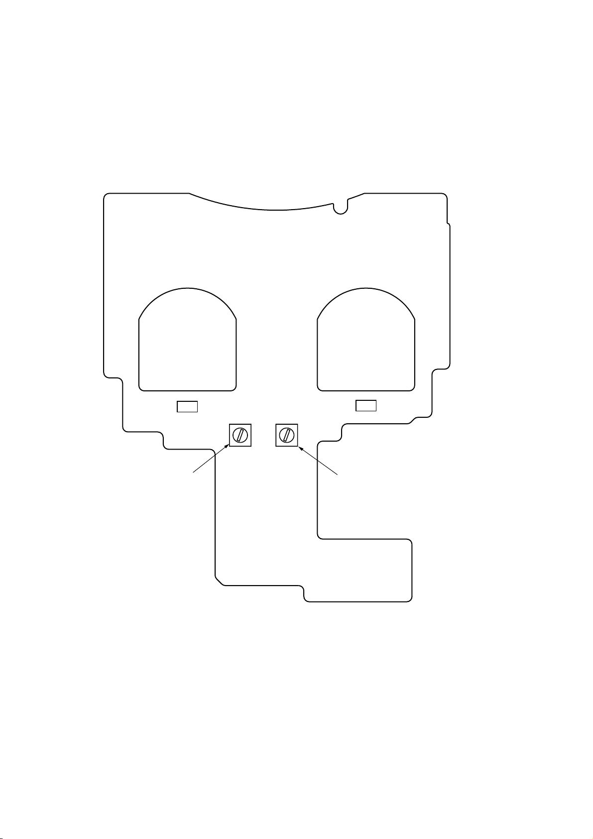
1. Reproduce the WAVE file (DIGITAL DATA) (1kHz, –12dBs)
standard signal.
2. Adjust RV2102 so that the pointer of the L-CH level meter
indicates the center of “12”.
3. Adjust RV2202 so that the pointer of the R-CH level meter
indicates the center of “12”.
Adjusting Location:
– AUDIO D/A BOARD (Component Side) –
CN2511
RV2102
(L-CH)
CN2521
RV2202
(R-CH)
18
SECTION 5
DIAGRAMS
PCM-D1
Note on Schematic Diagrams:
• All capacitors are in µF unless otherwise noted. (p: pF)
50 WV or less are not indicated except for electrolytics
and tantalums.
• All resistors are in Ω and 1/
specified.
• f : internal tolerance.
• C : panel designation.
• A : B+ Line.
•Power voltage is dc 6.0V and fed with regulated dc power
supply from battery terminal.
•Voltages and waveforms are dc with respect to ground
under no-signal (detuned) conditions.
no mark : PB
[]: REC
•Voltages are taken with a VOM (Input impedance 10 MΩ).
Voltage variations may be noted due to normal production
tolerances.
•Waveforms are taken with a oscilloscope.
Voltage variations may be noted due to normal production
tolerances.
• Circled numbers refer to waveforms.
• Signal path.
c : REC (DIGITAL)
L : REC (ANALOG)
J : PB (DIGITAL)
F : PB (ANALOG)
*
• The voltage and waveform of CSP (chip size package)
cannot be measured, because its lead layout is different
from that of conventional IC.
: Impossible to measure
∗
Replacement of IC6001, 8101 and 8201 used in this
set requires a special tool.
4
W or less unless otherwise
Note on Printed Wiring Boards:
• X : parts extracted from the component side.
• : Pattern from the side which enables seeing.
(The other layers' patterns are not indicated.)
Caution:
Pattern face side: Parts on the pattern face side seen from the
(Side B) pattern face are indicated.
Parts face side: Parts on the parts face side seen from the
(Side A) parts face are indicated.
Replacement of IC6001, 8101 and 8201 used in this set
*
requires a special tool.
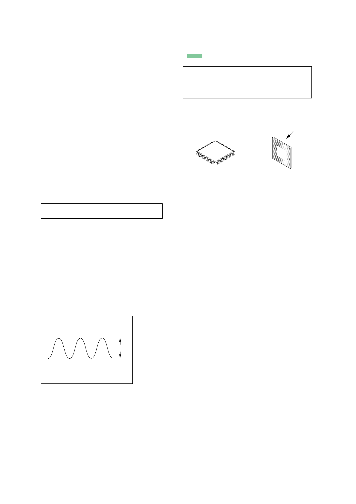
• Lead layouts
Lead layout of
conventional IC
CSP (chip size package)
surface
• Waveform
— MAIN Board —
IC7001 ws (X0)
1
11.095MHz
1V/DIV, 50nsec/DIV
3Vp-p
19
PCM-D1
d
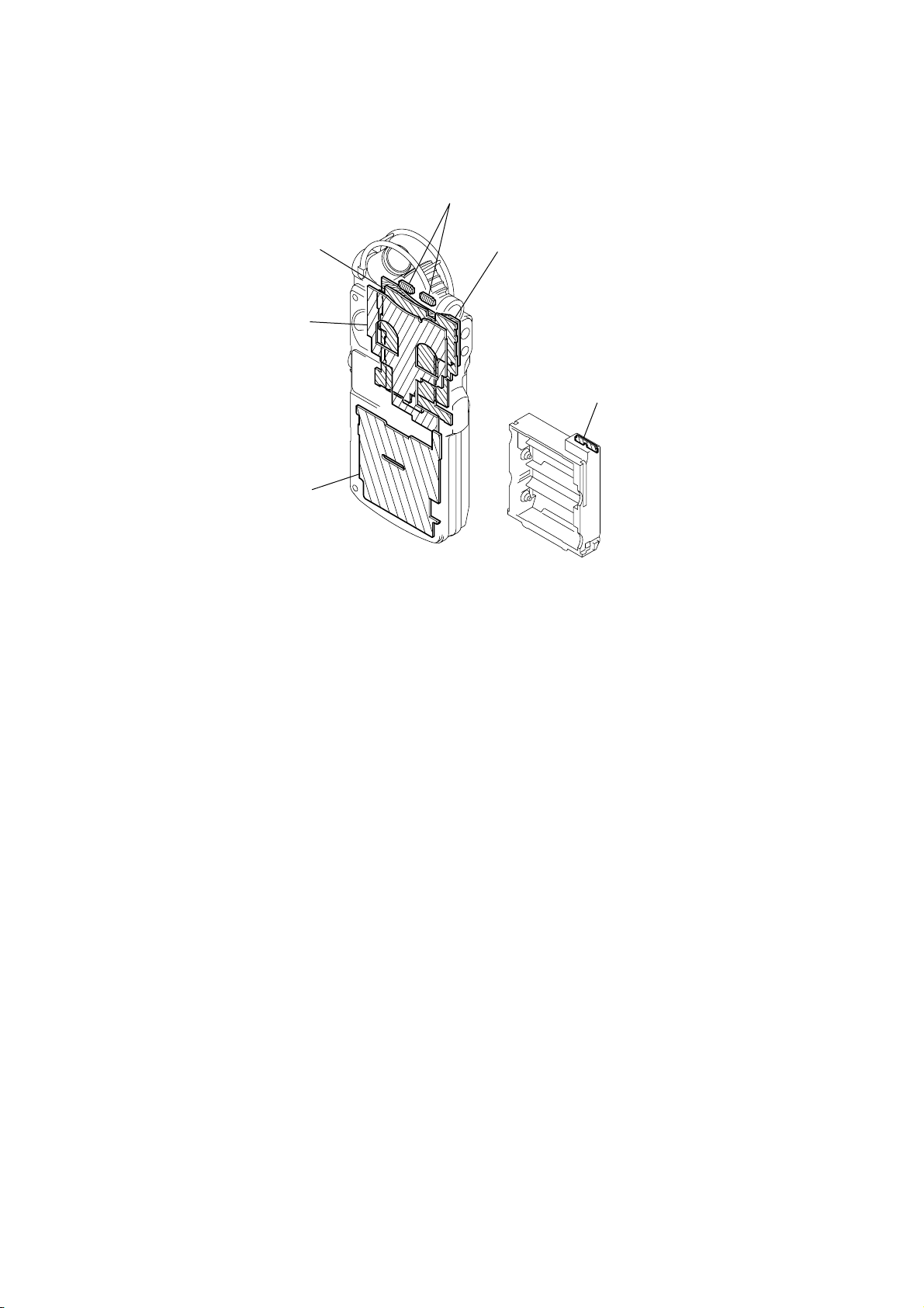
• CIRCUIT BOARDS LOCATION
AMP board
AUDIO A/D board
AUDIO D/A board
POWER board
MAIN board
BATTERY boar
20
 Loading...