

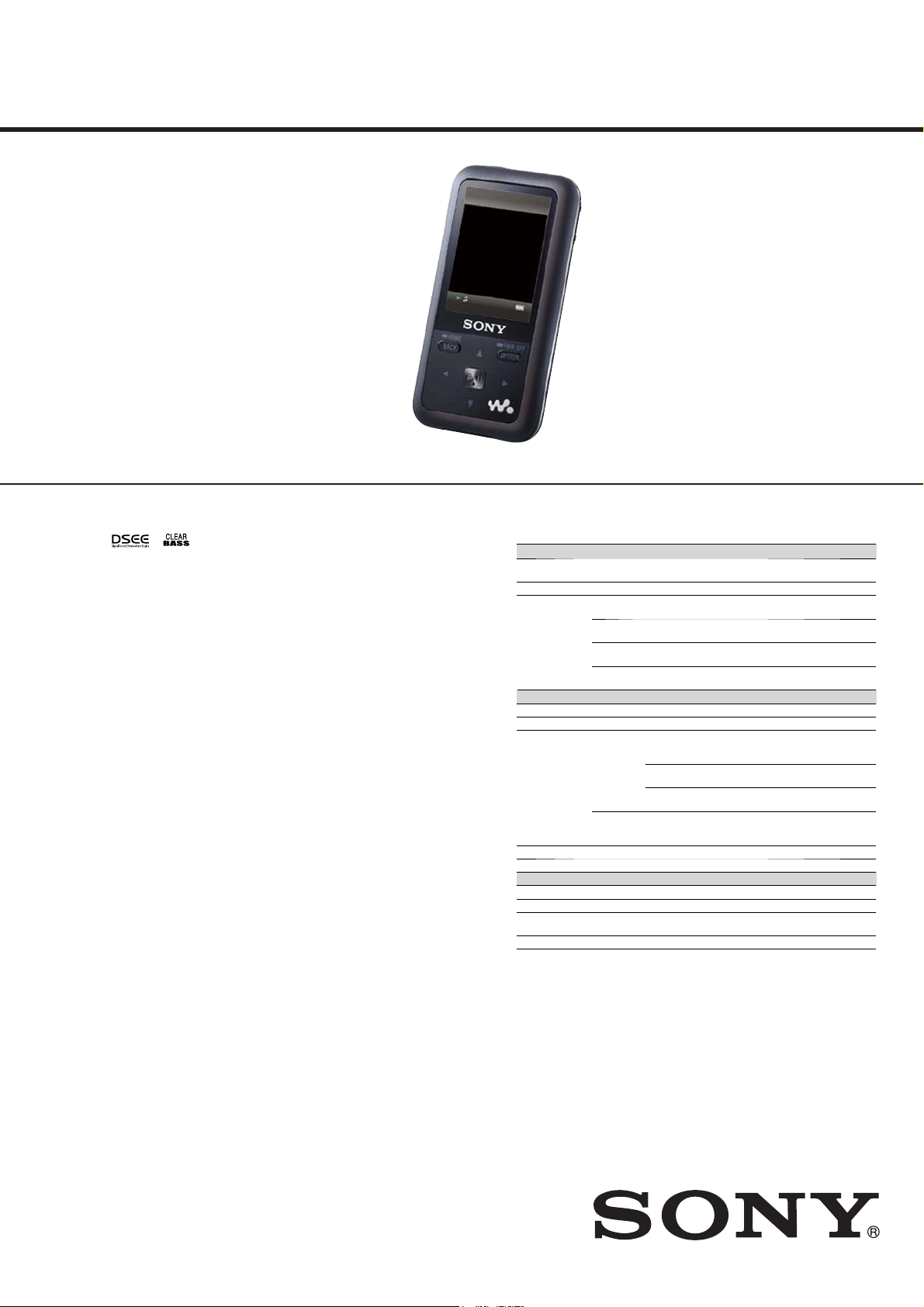
NWZ-S515/S516/S615F/
S616F/S618F
SERVICE MANUAL
Ver. 1.5 2008.09
ATRAC is trademark of Sony Corporation.
“WALKMAN” and “WALKMAN” logo are registered trademarks of Sony
Corporation.
and are trademarks of Sony Corporation.
Microsoft, Windows, Windows Vista and Windows Media are trademarks or
registered trademarks of Microsoft Corporation in the United States and/or
other countries.
Adobe, Adobe Reader and Adobe Flash Player are trademarks or registered
trademarks of Adobe Systems Incorporated in the United States and/or other
countries.
MPEG Layer-3 audio coding technology and patents licensed from
Fraunhofer IIS and Thomson.
IBM and PC/AT are registered trademarks of International Business
Machines Corporation.
Macintosh is a trademark of Apple Inc.
Pentium is a trademark or a registered trademark of Intel Corporation.
This software is based in part on the work of the Independent JPEG Group.
THIS PRODUCT IS LICENSED UNDER THE MPEG-4 VISUAL PATENT
PORTFOLIO LICENSE FOR THE PERSONAL AND NON-COMMERCIAL
USE OF A CONSUMER FOR
(i) ENCODING VIDEO IN COMPLIANCE WITH THE MPEG-4 VISUAL
STANDARD (“MPEG-4 VIDEO”) AND/OR
(ii) DECODING MPEG-4 VIDEO THAT WAS ENCODED BY A
CONSUMER ENGAGED IN A PERSONAL AND NON-COMMERCIAL
ACTIVITY AND/OR WAS OBTAINED FROM A VIDEO PROVIDER
LICENSED BY MPEG LA TO PROVIDE MPEG-4 VIDEO.
NO LICENSE IS GRANTED OR SHALL BE IMPLIED FOR ANY OTHER
USE. ADDITIONAL INFORMATION INCLUDING THAT REL ATING TO
PROMOTIONAL, INTERNAL AND COMMERCIAL USES AND
LICENSING MAY BE OBTAINED FROM MPEG LA, LLC. SEE
HTTP://WWW.MPEGLA.COM
THIS PRODUCT IS LICENSED UNDER THE AVC PATENT PORTFOLIO
LICENSE FOR THE PERSONAL AND NON-COMMERCIAL USE OF A
CONSUMER TO
(i) ENCODE VIDEO IN COMPLIANCE WITH THE AVC STANDARD
(“AVC VIDEO”) AND/OR
(ii) DECODE AVC VIDEO THAT WAS ENCODED BY A CONSUMER
ENGAGED IN A PERSONAL AND
NON-COMMERCIAL ACTIVITY AND/OR WAS OBTAINED FROM A
VIDEO PROVIDER LICENSED TO PROVIDE AVC VIDEO. NO LICENSE
IS GRANTED OR SHALL BE IMPLIED FOR ANY OTHER USE.
ADDITIONAL INFORMATION MAY BE OBTAINED FROM MPEG LA,
L.L.C. SEE HTTP://MPEGLA.COM
US and foreign patents licensed from Dolby Laboratories.
All other trademarks and registered trademarks are trademarks or registered
trademarks of their respective holders. In this manual,
specified.
This product is protected by certain intellectual property rights of Microsoft
Corporation. Use or distribution of such technology outside of this product is
prohibited without a license from Microsoft or an authorized Microsoft
subsidiary.
Content providers are using the digital rights management technology for
Windows Media contained in this device (“WM-DRM”) to protect the integrity
of their content (“Secure Content”) so that their intellectual property, including
copyright, in such content is not misappropriated.
This device uses WM-DRM software to play Secure Content (“WM-DRM
Software”). If the security of the WM-DRM Software in this device has been
compromised, owners of Secure Content (“Secure Content Owners”) may
request that Microsoft revoke the WM-DRM Software’s right to acquire new
licenses to copy, display and/or play Secure Content. Revocation does not alter
the WM-DRM Software’s ability to play unprotected content. A list of revoked
WM-DRM Software is sent to your device whenever you download a license
for Secure Content from the Internet or from a PC. Microsoft may, in
conjunction with such license, also download revocation lists onto your device
on behalf of Secure Content Owners.
Program ©2007 Sony Corporation
Documentation ©2007 Sony Corporation
TM
and ® marks are not
US Model
Canadian Model
E Model
Australian Model
Chinese Model
Tourist Model
NWZ-S615F/S616F/S618F
AEP Model
NWZ-S515/S516/S615F/
S616F/S618F
UK Model
NWZ-S515/S516/S616F/S618F
SPECIFICATIONS
Supported le format
Music
File format MP3(MPEG1 Layer3) file format, ASF file format, MP4 file format, Wave-Riff file
File extension MP3 (.mp3), WMA (.wma), AAC-LC*
Codec MP3 Bit rate: 32 to 320 kbps (Supports variable bit rate (VBR))
Video (NWZ-S615F/S616F/S618F only)
File format MP4 file format, “Memory Stick” video format
File extension .mp4, .m4v
Codec Video AVC
File size Max. 2 GB
The number of files Max. 1,000
4
Photo*
File format Compatible with DCF 2.0/Exif 2.21file format
File extension .jpg
Codec Profile: Baseline Profile
The number of files Max. 10,000
*1Copyright protected AAC-LC files cannot be played back.
2
Sampling frequency may not correspond to all encoders.
*
3
Non-standard bit rates or non-guaranteed bit rates are included depending on the
*
sampling frequency.
4
Some photo files cannot be played back, depending on their file formats.
*
format
WMA Bit rate: 32 to 192 kbps (Supports variable bit rate (VBR))
AAC-LC*
Linear PCM Bit rate: 1,411 kbps
Audio AAC-LC Channel number: Max. 2 channels
Number of pixels: Max. 4,000 × 4,000 pixels (16,000,000 pixels)
Sampling frequency*
Sampling frequency*
1
Bit rate: 16 to 320 kbps (Supports variable bit rate (VBR))*
Sampling frequency*2: 8, 11.025, 12, 16, 22.05, 24, 32, 44.1, 48 kHz
Sampling frequency*
(H.264/AVC)
MPEG-4 Profile: Simple Profile
Frame rate: Max. 30 fps
Resolution: Max. QVGA (320 × 240)
1
(.mp4, .m4a, .3gp), Linear PCM (.wav)
2
: 32, 44.1, 48 kHz
2
: 44.1 kHz
2
: 44.1 kHz
Profile: Baseline Profile
Level: Max. 1.3
Bit rate: Max. 768 kbps
Bit rate: Max. 2,500 kbps
Sampling frequency*
Bit rate: Max. 288 kbps per 1 channel
2
: 24, 32, 44.1, 48 kHz
3
– Continued on next page –
DIGITAL MEDIA PLAYER
9-887-816-06
2008I05-1
2008.09
©
Sony Corporation
Audio&Video Business Group
Published by Sony Techno Create Corporation
NWZ-S515/S516/S615F/S616F/S618F
Maximum recordable number of songs and time (Approx.)
The approximate times are based on the case in which you transfer or record only 4
minutes songs (not including videos (NWZ-S615F/S616F/S618F only) and photos) in the
MP3 format. Other playable audio file format song numbers and times may differ from
MP3 format.
Bit rate Songs Time Songs Time
48 kbps 1,150 76 hr. 40 min. 2,450 163 hr. 20 min.
64 kbps 885 59 hr. 00 min. 1,850 123 hr. 20 min.
128 kbps 440 29 hr. 20 min. 925 61 hr. 40 min.
256 kbps 220 14 hr. 40 min. 460 30 hr. 40 min.
320 kbps 175 11 hr. 40 min. 370 24 hr. 40 min.
Bit rate Songs Time
48 kbps 5,050 336 hr. 40 min.
64 kbps 3,750 250 hr. 00 min.
128 kbps 1,850 123 hr. 20 min.
256 kbps 945 63 hr. 00 min.
320 kbps 840 56 hr. 00 min.
NWZ-S515/S615F NWZ-S516/S616F
NWZ-S618F
Maximum recordable time of videos (Approx.) (NWZ-S615F/S616F/S618F only)
The approximate recordable times are estimated in the case where only videos are
transferred. The time may differ, depending on the conditions under which the player is
used.
Bit rate Time Time Time
Video Format: 384 kbps
Audio Format: 128 kbps
Video Format: 768 kbps
Audio Format: 128 kbps
NWZ-S615F NWZ-S616F NWZ-S618F
7 hr. 10 min. 15 hr. 00 min. 30 hr. 40 min.
4 hr. 00 min. 8 hr. 30 min. 17 hr. 30 min.
Maximum recordable number of photos that can be transferred (Approx.)
Max. 10,000
Recordable number of photos may be less depending on file sizes.
Capacity (User available capacity)*
NWZ-S515: 2 GB (Approx. 1.71 GB = 1,840,840,704 bytes)
NWZ-S516: 4 GB (Approx. 3.57 GB = 3,840,704,512 bytes)
NWZ-S615F: 2 GB (Approx. 1.71 GB = 1,840,775,168 bytes)
NWZ-S616F: 4 GB (Approx. 3.57 GB = 3,840,638,976 bytes)
NWZ-S618F: 8 GB (Approx. 7.30 GB = 7,840,956,416 bytes)
1
Available storage capacity of the player may vary.
*
A portion of the memory is used for data management functions.
1
Output (headphones)
Frequency response
20 to 20,000 Hz (when playing data file, single signal measurement)
FM tuner (NWZ-S615F/S616F/S618F only)
FM Frequency range
87.5 to 108.0 MHz
IF (FM) (NWZ-S615F/S616F/S618F only)
375 kHz
Antenna (NWZ-S615F/S616F/S618F only)
Headphone cord antenna
Interface
Headphone: Stereo mini-jack
WM-PORT (multiple connecting terminal): 22 pins
Hi-Speed USB (USB 2.0 compliant)
Operating temperature
5 °C to 35 °C (41 °F to 95 °F)
Power source
Built-in rechargeable lithium-ion battery
USB power (from a computer via the supplied USB cable)
Charging time
USB-based charging
Approx. 3 hours (full charge), Approx.1.5 hours (approx. 80 %)
Battery life (continuous playback)
By setting as follows, a longer battery life can be expected.
e time below is approximated when “New Song Pop Up”, “Clear Stereo”, “DSEE
(Sound Enhance)”, “Dynamic Normalizer”, “Equalizer” and “VPT (Surround)” are
deactivated, and “Screensaver” is set to “Blank.”
Furthermore, for videos (NWZ-S615F/S616F/S618F only), the time approximated when
the brightness of the screen is set to “3.”
e time below may dier depending on ambient temperature or the status of use.
Music
Playback at MP3 128 kbps Approximately 33 hours Approximately 33 hours
Playback at WMA 128 kbps Approximately 33 hours Approximately 33 hours
Playback at AAC-LC 128 kbps Approximately 32 hours Approximately 32 hours
Playback at Linear PCM 1411 kbps Approximately 35 hours Approximately 35 hours
Video
(NWZ-S615F/S616F/S618F only)
Playback at MPEG-4 384 kbps
Playback at MPEG-4 768 kbps pproximately 8.5 hours
Playback at AVC 384 kbps pproximately 7.5 hours
Playback at AVC 768 kbps pproximately 7.5 hours
At receiving FM broadcasting
(NWZ-S615F/S616F/S618F only)
NWZ-S515/S516 NWZ-S615F/S616F/S618F
pproximately 9.5 hours
pproximately 24 hours
Display
1.82-inch, TFT color display with white LED-backlight, QVGA (240 × 320 pixels), 262,144
colors
Dimensions (w/h/d, projecting parts not included)
42.0 × 79.5 × 11.5 mm (1 11/16 × 3 1/4 × 15/32 inches)
Dimension (w/h/d)
42.0 × 79.5 × 11.5 mm (1 11/16 × 3 1/4 × 15/32 inches)
Mass
Approx. 50 g (Approx. 1.8 oz)
Supplied Accessories
Headphones (1)
USB cable*1 (1)
Attachment (1)
Use when connecting the player to the optional cradle, etc.
*2 *3
CD-ROM
(1)
– MP3 Conversion Tool
– Windows Media Player 11
– Operation Guide (PDF f le)
Quick Start Guide (1)
*1
Do not use any USB cable other than the supplied USB cable or the specif ed
optional dedicated cables.
*2
Do not attempt to play this CD-ROM in an audio CD player.
*3
Depending on the country/region in which you have purchased the player, the sup-
plied software may be different.
Design and specications are subject to change without notice.
2

NWZ-S515/S516/S615F/S616F/S618F
SECTION 1
SERVICING NOTES
TABLE OF CONTENTS
1. SERVICING NOTES ............................................. 3
2. GENERAL .................................................................. 5
3. DISASSEMBLY
3-1. Disassembly Flow .......................................................... 6
3-2. Case (Upper) Sub Assy ................................................... 6
3-3. LCD Sub Assy (LCD801) ............................................... 7
3-4. MAIN Board ................................................................... 7
3-5. Lithium Ion Battery ........................................................ 8
4. TEST MODE ............................................................ 9
5. DIAGRAMS
5-1. Block Diagram ................................................................ 16
5-2. Printed Wiring Board - MAIN Board (Side A) - ............ 18
5-3. Printed Wiring Board - MAIN Board (Side B) - ............ 19
5-4. Schematic Diagram - MAIN Board (1/10) - ................... 20
5-5. Schematic Diagram - MAIN Board (2/10) - ................... 21
5-6. Schematic Diagram - MAIN Board (3/10) - ................... 22
5-7. Schematic Diagram - MAIN Board (4/10) - ................... 23
5-8. Schematic Diagram - MAIN Board (5/10) - ................... 24
5-9. Schematic Diagram - MAIN Board (6/10) - ................... 25
5-10. Schematic Diagram - MAIN Board (7/10) - ................... 26
5-11. Schematic Diagram - MAIN Board (8/10) - ................... 27
5-12. Schematic Diagram - MAIN Board (9/10) - ................... 28
5-13. Schematic Diagram - MAIN Board (10/10) - ................. 29
6. EXPLODED VIEWS
6-1. Case (Upper) Section ...................................................... 42
6-2. LCD, MAIN Board Section ............................................ 43
6-3. Case (Lower) Section ...................................................... 44
7. ELECTRICAL PARTS LIST .............................. 45
UNLEADED SOLDER
Boards requiring use of unleaded solder are printed with the leadfree mark (LF) indicating the solder contains no lead.
(Caution: Some printed circuit boards may not come printed with
the lead free mark due to their particular size)
: LEAD FREE MARK
Unleaded solder has the following characteristics.
• Unleaded solder melts at a temperature about 40 °C higher
than ordinary solder.
Ordinary soldering irons can be used but the iron tip has to be
applied to the solder joint for a slightly longer time.
Soldering irons using a temperature regulator should be set to
about 350 °C.
Caution: The printed pattern (copper foil) may peel away if the
heated tip is applied for too long, so be careful!
• Strong viscosity
Unleaded solder is more viscous (sticky, less prone to f ow)
than ordinary solder so use caution not to let solder bridges
occur such as on IC pins, etc.
• Usable with ordinary solder
It is best to use only unleaded solder but unleaded solder may
also be added to ordinary solder.
NOTE THE IC301, IC302, IC303, IC404, IC405, IC501,
IC503, IC505, IC506, IC507, IC508, IC509, IC601, IC602,
IC701, IC751, IC752, IC802, IC803, IC901 AND IC903
ON THE MAIN BOARD REPLACING
When IC301, IC302, IC303, IC404, IC405, IC501, IC503, IC505,
IC506, IC507, IC508, IC509, IC601, IC602, IC701, IC751, IC752,
IC802, IC803, IC901 and IC903 on the MAIN board is damaged,
exchange the new MAIN board for the MAIN board which IC
damaged.
NOTE THE CN881 ON THE MAIN BOARD REPLACING
When CN881 on the MAIN board is damaged, exchange the new
MAIN board for the MAIN board which connector damaged.
Notes on chip component replacement
• Never reuse a disconnected chip component.
• Notice that the minus side of a tantalum capacitor may be damaged by heat.
Flexible Circuit Board Repairing
• Keep the temperature of soldering iron around 270 °C during
repairing.
• Do not touch the soldering iron on the same conductor of the
circuit board (within 3 times).
• Be careful not to apply force on the conductor when soldering
or unsoldering.
CAUTION
Danger of explosion if battery is incorrectly replaced.
Replace only with the same or equivalent type.
NOTE THE C104 AND C204 ON THE MAIN BOARD
REPLACING
When C104 and C204 on the MAIN board is damaged, exchange
the new MAIN board for the MAIN board which capacitor damaged.
System Requirements
Computer
IBM PC/AT or compatible computer preinstalled with the following Windows operating
systems*:
Windows XP Home Edition (Service Pack 2 or later) / Windows XP Professional
(Service Pack 2 or later) / Windows XP Media Center Edition (Service Pack 2 or later) /
Windows XP Media Center Edition 2004 (Service Pack 2 or later) / Windows XP Media
Center Edition 2005 (Service Pack 2 or later) / Windows Vista Home Basic / Windows
Vista Home Premium / Windows Vista Business / Windows Vista Ultimate
Not supported by 64 bit version OS.
Not supported by OSs other than above.
* Excluding OS Versions not supported by Microsoft.
CPU: Pentium III 1.0 GHz or higher
RAM: 128 MB or more (For Windows Vista, 512 MB or more)
Hard Disk drive: 380 MB or more of available space
Display:
Screen Resolution: 800 × 600 pixels (or higher) (recommended 1,024 × 768 or higher)
Colors: 8 bit or higher (recommended 16 bit)
CD-ROM drive (supporting Digital Music CD playback capabilities using WDM)
To create original CDs, a CD-R/RW drive is required.
Sound board
USB port (Hi-Speed USB is recommended)
Internet Explorer 6.0 or later, Windows Media Player 10 or 11 (Windows Media Player
11 recommended. Some computers that already have Windows Media Player 10
installed may encounter le limitation (AAC, video* les, etc.) that can be transferred by
dragging and dropping.).
* NWZ-S615F/S616F/S618F only
Adobe Flash Player 8 or higher needs to be installed.
Broadband Internet connection is required to use Electronic Music Distribution (EMD)
or to visit the web site.
We do not guarantee operation for all computers even if they meet the above System
Requirements.
Not supported by the following environments:
Personally const ructed c omputers or operat ing systems
An environment that is an upgrade of the original manufacturer-installed operating
system
Multi-boot environment
Multi-monitor environment
Macintosh
3
NWZ-S515/S516/S615F/S616F/S618F
Ver. 1.4
NOTE THE MAIN BOARD REPLACING
When the MAIN board is replaced, format it according to the following.
Formatting Memory
You can format the built-in flash memory of the player.
If the memory is formatted, all data and settings will be erased. Be sure to
verify the data stored in memory prior to formatting and export any important
data to the hard disk of your computer.
Note
This function is only available in the pause mode.
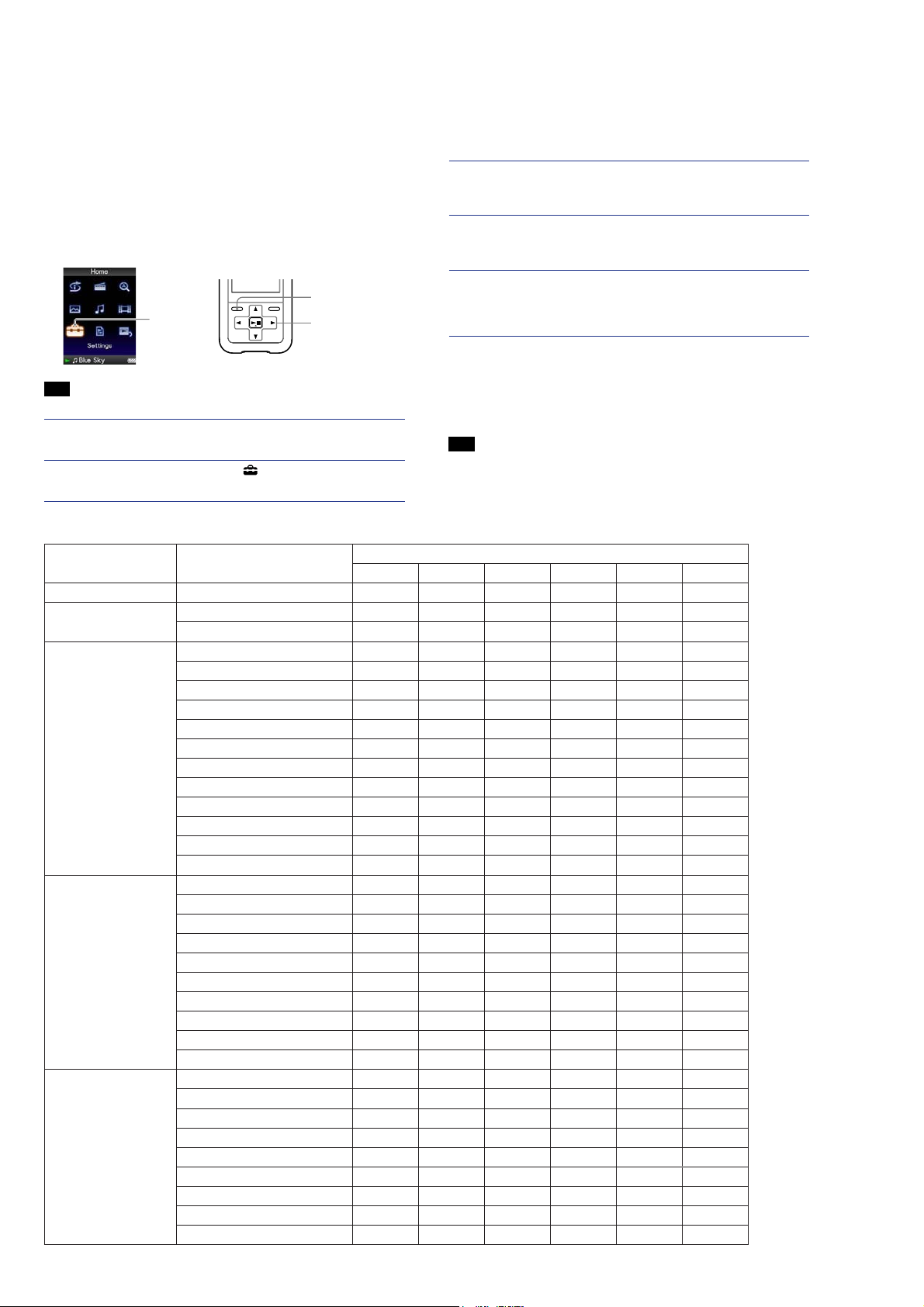
Press and hold the BACK/HOME button in the pause mode until the
Home menu appears.
Press the /// button to select (Settings), and then press
the button to conrm.
Settings
(Format)
BACK/HOME
button
5-way button
Press the /// button to select “Common Settings,” and then
press the button to conrm.
The list of “Common Settings” options appears.
Press the /// button to select “Format,” and then press the
button to conrm.
“All data including songs will be deleted. Proceed?” appears.
Press the / button to select “Yes,” and then press the button
to conrm.
“All data will be deleted. Proceed?” appears.
Press the / button to select “Yes,” and then press the button
to conrm.
While the memory is being formatted, an animated display appears.
When initialization finishes, “Memory formatted.” appears.
To cancel the operation
Select “No” in step or and press the button to confirm. You can also
cancel the operation by pressing the BACK/HOME button in step
To return to the previous menu
Press the BACK/HOME button.
Note
Do not format the built-in flash memory using Windows Explorer, or the software you
used to transfer the data.
or .
COLOR VARIATION
Model Destination
NWZ-S515 AEP, UK
NWZ-S516 AEP
UK
NWZ-S615F US
US (Circuit City model)
US (Target model)
US (Valentine’s Day model)
US (Mother’s Day model)
Canadian
AEP
French
East European
E, Australian, Tourist
Mexican
Chinese
NWZ-S616F US
US (Circuit City model)
Canadian
AEP
UK
French
East European
E, Australian, Tourist
Mexican
Chinese
NWZ-S618F US
Canadian
AEP
UK
French
East European
E, Australian, Tourist
Mexican
Chinese
Color
Black White Pink Blue Silver Red
zzzz
zzzz
z
zzzz
zz
z
zz
z
zzz
zzz
zzz
zzz
zzz
zz z
zzzz
zzzz
z
zzzz
zzz
zzz
zzz
zzz
zzzz z
zzz
zz z z
z
zz
zzz
zzz
zz
zzz
zz
z
z
4
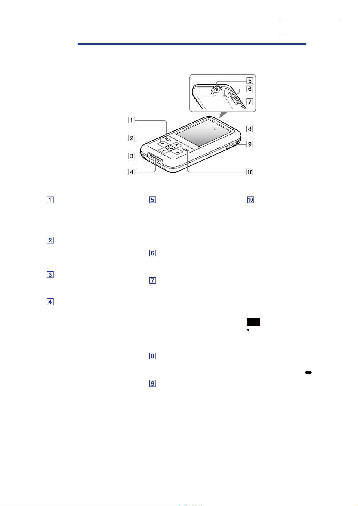
Parts and Controls
NWZ-S515/S516/S615F/S616F/S618F
SECTION 2
GENERAL
This section is extracted
from instruction manual.
Front
BACK/HOME button*
Press to go up one list screen level, or
to return to the previous menu.
Press and hold the BACK/HOME
button to display the Home menu.
5-way button*
Starts playback and enables
navigation of the player’s on-screen
menus.
RESET button
Resets the player when you press the
RESET button with a small pin, etc..
WM-PORT jack
Use this jack to connect the supplied
USB cable, or optional peripheral
devices, such as supported
accessories for the WM-PORT.
1
2
Rear
Headphone jack
For connecting the headphones.
Insert the jack pin until it clicks into
place. If the headphones are
connected improperly, the sound
from the headphones may not sound
right.
Strap hole
is is used to attach a strap (sold
separately).
HOLD switch
You can protect the player against
accidental operation by using the
HOLD switch when carrying it. By
sliding the HOLD switch in the
direction of the arrow, all operation
buttons are disabled. If you slide the
HOLD switch to the opposite
position, the HOLD function is
released.
Display
e display may vary, depending on
functions.
VOL +*2/– button
Adjusts the volume.
OPTION/PWR OFF button*
1
Displays the option menu.
If you press and hold the OPTION/
PWR OFF button, the screen turns
off and the player enters the standby
mode. If you press any button while
the player is in the standby mode,
the “Now Playing” screen, etc.,
appears and the player is ready for
operation. Furthermore, if you leave
the player in the standby mode for
about a day, the player turns
completely off automatically. If you
press any button when the player is
turned off, the start up screen
appears rst, then the “Now Playing”
screen appears.
Note
e player consumes battery power very
slightly even when it is in the standby
mode. erefore, the player might
turn completely off in a short time,
depending on the power remaining in
the battery.
1
Functions of marked with on the
*
player are activated if you press and hold
the corresponding buttons.
2
ere are tactile dots. Use them to help
*
with button operations.
5
NWZ-S515/S516/S615F/S616F/S618F
SECTION 3
DISASSEMBLY
• This set can be disassembled in the order shown below.
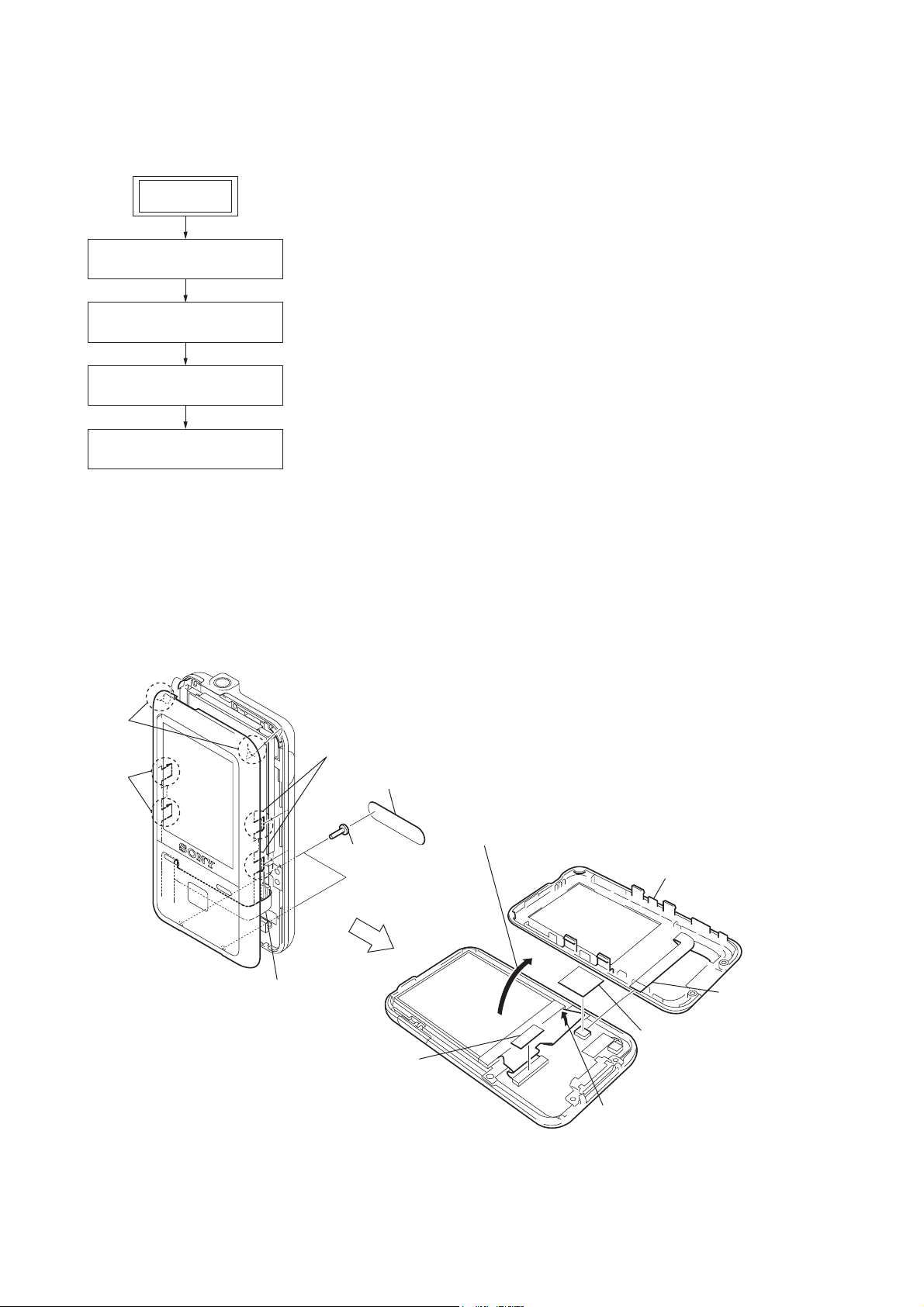
3-1. DISASSEMBLY FLOW
SET
3-2. CASE (UPPER) SUB ASSY
(Page 6)
3-3. LCD SUB ASSY (LCD801)
(Page 7)
3-4. MAIN BOARD
(Page 7)
3-5. LITHIUM ION BATTERY
(Page 8)
Note: Follow the disassembly procedure in the numerical order given.
3-2. CASE (UPPER) SUB ASSY
two claws
two claws
two claws
sheet switch
Note: Take care not to break
the sheet switch.
saranet cushion
model name label
two screws
(1.4)
Open the case (upper) sub assy
in the direction of arrow ".
"
#
sheet (SW CN)
R case (upper) sub assy
sheet switch
(CN881)
Lift up the LCD flexible board
in the direction of arrow #.
6
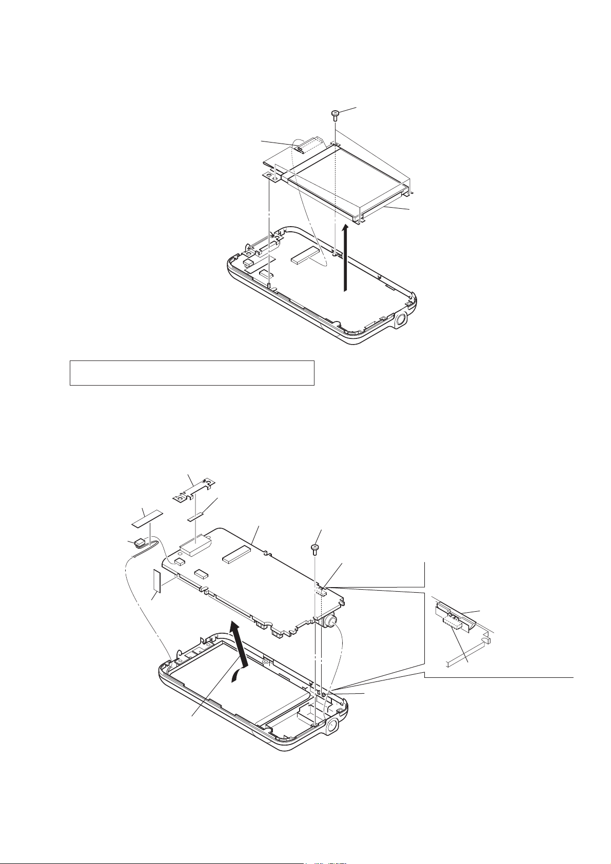
3-3. LCD SUB ASSY (LCD801)
LCD flexible board
(CN801)
NWZ-S515/S516/S615F/S616F/S618F
Ver. 1.3
four screws
(B1.4)
LCD sub assy
(LCD801)
Note: When the LCD SUB ASSY (LCD801) is replaced, refer to
SUPPLEMENT-2.
3-4. MAIN BOARD
holder (multi)
sheet (multi)
BATT wire sheet
MAIN board
connector
(CN901)
sheet (PWB rib)
screw (B1.4)
switch (S602)
Note: On installation of knob (hold),
adjust the position of switch (S602)
and knob (hold).
knob (hold)
Remove the MAIN board
in the direction of the arrow.
switch (S602)
knob (hold)
7
NWZ-S515/S516/S615F/S616F/S618F
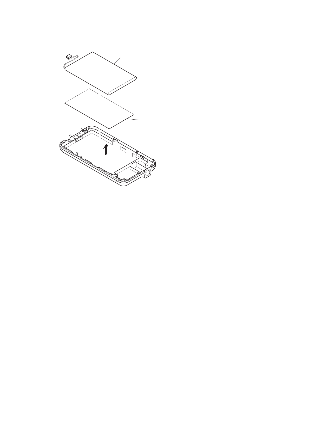
3-5. LITHIUM ION BATTERY
lithium ion battery
adhesive sheet (BATT)
Note: Adhesive sheet (BATT) cannot re-used.
Please replace to brand-new part ones
adhesive sheet (BATT) is removed.
8
NWZ-S515/S516/S615F/S616F/S618F
SECTION 4
TEST MODE
Note: Information on the test mode must correspond in enough
security. When the leakage has been revealed by any
chance, the source of information is specif ed.
1. SETTING THE TEST MODE
Note: Perform the test mode in the state of 3.6 V or more in the battery
voltage.
Setting method:
1. Turn the power on.
2. Press the [BACK] key for 1.5 seconds or more, the home menu
is displayed.
3. Slide the [HOLD] key to set the hold on.
4. While pressing the [OPTION] key, press the key as following
order.
[v] → [v] → [V] → [V] → [B] → [b] → [v] → [V] → [v] →
[V] → [B] → [u]
5. The set reboots when the [HOLD] key is slided to set the hold
off, and the color bar is displayed in the liquid crystal display.
6. Enter the test mode when the [BACK] key is pressed in the
state of step 5.
Note: The destination setting and sound pressure regulation setting can-
not be executed by this test mode.
2. RELEASING THE TEST MODE
1. Display the major item selection screen.
2. Press the [
] key to select the “SURE ?”.
[
B
]/[V] key to select the “EXITTEST”, and press the
v
3. Press the [u] key, turn the power off and release the test
mode.
3. CONFIGURATION OF THE TEST MODE
Major item
<> key
#C
<> key
Major item switching:
<>/ <> key
W
7
4-1-1. Power supply voltage check
This mode is used in case power supply voltage in the state where
all power supply lines are starting is checked.
Checking method:
1. Enter the test mode.
2. Press the [v]/[V] key to select the “POWER”, and press the
[
] key to enter the minor item.
B
3. Press the [v]/[V] key to select the “VCHK”.
4. Press the [
] key, all power supply lines are started.
u
liquid crystal display
POWER VCHK
START
In this state, the power supply voltage of each power supply
line can be conf rmed by measuring the voltage.
5. Press the [BACK] key, return to minor item selection screen.
4-1-2. Consumption current (audio playback) check
This mode is used in case consumption current (audio playback)
is checked in the state where “1 kHz 0 dBs L-ch/R-ch VOLUME:
15” audio signal is outputed.
Minor item switching:
<>/ <> key
W
7
key
<>
key
V
Automatic
Finish
Result
Start
or
Minor item
<#"$,>
4. OPERATION OF THE TEST MODE
4-1. Power
liquid crystal display
MPTAPP MENU
POWER VCHK
AUDIO ACHK
VIDEO DSVCHK
OTHER CHGCHK
CLESTE BATTCHK
DAC
FM
SHUTDOWN
EXITTEST
Checking method:
1. Enter the test mode.
2. Press the [v]/[V] key to select the “POWER”, and press the
[
] key to enter the minor item.
B
3. Press the [
]/[V] key to select the “ACHK”.
v
4. Press the [u] key, “1 kHz 0 dBs L-ch/R-ch VOLUE: 15”
audio signal is outputed.
liquid crystal display
POWER ACHK
1kHz 0dBs L/Rch
HPOUT [ VOL: 15 ]
START
5. In this state, each time the [OPTION] key is pressed, LCD
back light on/off switch is performed.
6. Press the [BACK] key, return to minor item selection screen.
9
NWZ-S515/S516/S615F/S616F/S618F
4-1-3. Standby current check
This mode is used in case standby current is checked.
Checking method:
1. Enter the test mode.
2. Press the [v]/[V] key to select the “POWER”, and press the
[B] key to enter the minor item.
3. Press the [
]/[V] key to select the “DSVCHK”.
v
4. Press the [u] key, enter the state of the deep sleep.
5. Press the [BACK] key, release the state of the deep sleep.
liquid crystal display
POWER DSVCHK
OK
6. Press the [BACK] key, return to minor item selection screen.
4-1-5. Battery voltage detection check
This mode is used in case battery voltage is checked.
Checking method:
1. Enter the test mode.
2. Press the [v]/[V] key to select the “POWER”, and press the
[B] key to enter the minor item.
3. Press the [
]/[V] key to select the “BATTCHK”.
v
4. Press the [u] key, the battery voltage is displayed.
When the battery voltage cannot be conf rmed, “ERROR” is
displayed.
liquid crystal display
POWER BATTCHK
X.XXXV
X.XXXV: Battery voltage
4-1-4. Charge current check
This mode is used in case charge current is checked.
Checking method:
1. Enter the test mode.
2. Press the [
] key to enter the minor item.
[
B
]/[V] key to select the “POWER”, and press the
v
3. Press the [v]/[V] key to select the “CHGCHK”.
4. Press the [u] key, the charge setting is displayed.
liquid crystal display
POWER CHGCHK
AC
AC
5. In this state, each time the [OPTION] key is pressed, the port
setting for the charge is changed as shown in the table below.
6. Press the [BACK] key, return to minor item selection screen.
4-2. Audio
While playing the audio track, it's in a repeat state. If [BACK] key
is pressed, it's stopped.
Press the [VOL +] key to switch the HP/LINE.
liquid crystal display
MPTAPP MENU
POWER
AUDIO OUTPUT
VIDEO SN
OTHER F1
CLESTE F2
DAC SEPLR
FM SEPRL
SHUTDOWN MAXOUT
EXITTEST NMLZR
SPCHK
Port control
Display CHG_XCHGEN CHG_PEN1 CHG_PEN2
AC L H H
USB500 L H H
USB100 L H L
6. Press the [BACK] key, return to minor item selection screen.
10
NWZ-S515/S516/S615F/S616F/S618F
4-2-1. Output check
“1 kHz 0 dBs L-ch/R-ch VOLUME: 25” audio signal is outputted.
Checking method:
1. Enter the test mode.
2. Press the [v]/[V] key to select the “AUDIO”, and press the [B]
key to enter the minor item.
3. Press the [
4. Press the [
]/[V] key to select the “OUTPUT”.
v
] key, “1 kHz 0 dBs L-ch/R-ch VOLUME: 25”
u
audio signal is outputted.
liquid crystal display
AUDIO OUTPUT
1kHz 0dBs L/Rch
HPOUT [ VOL: 25 ]
START
4-2-3. Frequency characteristic 1 check
“20 Hz 0 dBs L-ch/R-ch VOLUME: 25” audio signal is outputted.
Checking method:
1. Enter the test mode.
2. Press the [v]/[V] key to select the “AUDIO”, and press the [B]
key to enter the minor item.
3. Press the [
4. Press the [
]/[V] key to select the “F1”.
v
] key, “20 Hz 0 dBs L-ch/R-ch VOLUME: 25”
u
audio signal is outputted.
liquid crystal display
AUDIO F1
20Hz 0dBs L/Rch
HPOUT [ VOL: 25 ]
START
5. Press the [BACK] key, return to minor item selection screen.
4-2-2. S/N check
“Inf nity Zero VOLUME: 30” audio signal is outputted.
Checking method:
1. Enter the test mode.
2. Press the [v]/[V] key to select the “AUDIO”, and press the [B]
key to enter the minor item.
3. Press the [v]/[V] key to select the “SN”.
4. Press the [u] key, “Inf nity Zero VOLUME: 30” audio signal
is outputted.
liquid crystal display
AUDIO SN
Inf nity Zero
HPOUT [ VOL: 30 ]
START
5. Press the [BACK] key, return to minor item selection screen.
5. Press the [BACK] key, return to minor item selection screen.
4-2-4. Frequency characteristic 2 check
“20 kHz 0 dBs L-ch/R-ch VOLUME: 25” audio signal is outputted.
Checking method:
1. Enter the test mode.
2. Press the [v]/[V] key to select the “AUDIO”, and press the [B]
key to enter the minor item.
3. Press the [v]/[V] key to select the “F2”.
4. Press the [
] key, “20 kHz 0 dBs L-ch/R-ch VOLUME: 25”
u
audio signal is outputted.
liquid crystal display
AUDIO F2
20kHz 0dBs L/Rch
HPOUT [ VOL: 25 ]
START
5. Press the [BACK] key, return to minor item selection screen.
11
NWZ-S515/S516/S615F/S616F/S618F
4-2-5. CH separation (L-ch) check
“1 kHz 0 dBs L-ch VOLUME: 25” audio signal is outputted.
Checking method:
1. Enter the test mode.
2. Press the [v]/[V] key to select the “AUDIO”, and press the [B]
key to enter the minor item.
3. Press the [
]/[V] key to select the “SEPLR”.
v
4. Press the [u] key, “1 kHz 0 dBs L-ch VOLUME: 25” audio
signal is outputted.
liquid crystal display
AUDIO SEPLR
1kHz 0dBs Lch
HPOUT [ VOL: 25 ]
START
5. Press the [BACK] key, return to minor item selection screen.
4-2-6. CH separation (R-ch) check
“1 kHz 0 dBs R-ch VOLUME: 25” audio signal is outputted.
Checking method:
1. Enter the test mode.
2. Press the [
]/[V] key to select the “AUDIO”, and press the [B]
v
key to enter the minor item.
3. Press the [
]/[V] key to select the “SEPRL”.
v
4. Press the [u] key, “1 kHz 0 dBs R-ch VOLUME: 25” audio
signal is outputted.
liquid crystal display
AUDIO SEPRL
1kHz 0dBs Rch
HPOUT [ VOL: 25 ]
4-2-7. Maximum output check
“1 kHz 0 dBs L-ch/R-ch VOLUME: 30” (Headphone output when
AVLS operates: “1 kHz 0 dBs L-ch/R-ch VOLUME: 13”) audio
signal is outputted.
Checking method:
1. Enter the test mode.
2. Press the [
]/[V] key to select the “AUDIO”, and press the [B]
v
key to enter the minor item.
3. Press the [
]/[V] key to select the “MAXOUT”.
v
4. Press the [u] key, “1 kHz 0 dBs L-ch/R-ch VOLUME: 30”
(Headphone output when AVLS operates: “1 kHz 0 dBs L-ch/
R-ch VOLUME: 13”) audio signal is outputted.
liquid crystal display
AUDIO MAXOUT
1kHz 0dBs L/Rch
HPOUT [ VOL: 30 ]
AVLS OFF
START
5. In this state, each time the [OPTION] key is pressed, AVLS
on/off switch is performed.
6. Press the [BACK] key, return to minor item selection screen.
4-2-8. Normalizer check
“1 kHz – 24 dBs L-ch/R-ch VOLUME: 30” audio signal is outputted.
Checking method:
1. Enter the test mode.
2. Press the [v]/[V] key to select the “AUDIO”, and press the [B]
key to enter the minor item.
3. Press the [v]/[V] key to select the “NMLZR”.
4. Press the [u] key, “1 kHz – 24 dBs L-ch/R-ch VOLUME:
30” audio signal is outputted.
liquid crystal display
START
5. Press the [BACK] key, return to minor item selection screen.
12
AUDIO NMLZR
1kHz –24dBs L/Rch
HPOUT [ VOL: 30 ]
START
5. Press the [BACK] key, return to minor item selection screen.
NWZ-S515/S516/S615F/S616F/S618F
4-2-9. Sound pressure regulation level check
“1 kHz 0 dBs L-ch/R-ch VOLUME: 30” audio signal is outputted.
Checking method:
1. Enter the test mode.
2. Press the [v]/[V] key to select the “AUDIO”, and press the [B]
key to enter the minor item.
3. Press the [
4. Press the [
]/[V] key to select the “SPCHK”.
v
] key, “1 kHz 0 dBs L-ch/R-ch VOLUME: 30”
u
audio signal is outputted.
liquid crystal display
AUDIO SPCHK
1kHz 0dBs L/Rch
HPOUT [ VOL: 30 ]
START
4-4. Other
liquid crystal display
MPTAPP MENU
POWER
AUDIO
VIDEO
OTHER CLOCK
CLESTE KEY
DAC FORMAT
FM DEST
SHUTDOWN SPSET
EXITTEST FWVER
NCAPCHK
4-4-1. Clock check
The movement of an internal clock is conf rmed.
Checking method:
1. Enter the test mode.
2. Press the [v]/[V] key to select the “OTHER”, and press the [B]
key to enter the minor item.
3. Press the [
]/[V] key to select the “CLOCK”.
v
4. Press the [u] key, date and time are displayed.
5. Press the [BACK] key, return to minor item selection screen.
4-3. Video
liquid crystal display
MPTAPP MENU
POWER
AUDIO
VIDEO — LCD
OTHER
CLESTE
DAC
FM
SHUTDOWN
EXITTEST
4-3-1. LCD display check
Liquid crystal display is checked.
Checking method:
1. Enter the test mode.
2. Press the [v]/[V] key to select the “VIDEO”, and press the [B]
key to select the “LCD”.
3. Press the [u] key, all black is displayed on the liquid crystal
display.
4. In this state, each time the [OPTION] key is pressed, the screen
display changes in the following order.
liquid crystal display
OTHER CLOCK
XX, XX XX XXXX
##:##:##.######
START
XX, XX XX XXXX : Date
##:##:##.###### : Time
“START” changes into “OK” if the movement of an internal
clock is conf rmed.
5. Press the [BACK] key, return to minor item selection screen.
All black (default) → All red → All green → All blue → All
white → Color bar → Maximum drawing size conf rmation
Maximum drawing size conf rmation:
All blue (All sides are red) is displayed. Whether red in all
sides is seen is conf rmed.
5. In this state, each time the [VOL –] key is pressed, LCD back
light brightness min/max/middle switch is performed.
6. Press the [BACK] key, return to minor item selection screen.
13

NWZ-S515/S516/S615F/S616F/S618F
4-4-2. Key check
The operation of the key is conf rmed.
Checking method:
1. Enter the test mode.
2. Press the [v]/[V] key to select the “OTHER”, and press the [B]
key to enter the minor item.
3. Press the [
]/[V] key to select the “KEY”.
v
4. Press the [u] key, all keys are displayed.
liquid crystal display
UP VOL+
DOWN OPTION
HOLD BACK
OTHER KEY
REW PLAY FF VOL–
START
5. The character corresponding to the key is selected every time
the key is pressed. “START” changes into “OK” if all keys are
pressed.
6. Slide the [HOLD] key from ON to OFF, return to minor item
selection screen.
4-4-6. Firmware version check
The f rmware version is displayed.
Checking method:
1. Enter the test mode.
2. Press the [v]/[V] key to select the “OTHER” and press the [B]
key to enter the minor item.
3. Press the [
]/[V] key to select the “FWVER”.
v
4. Press the [u] key, the f rmware version is displayed.
liquid crystal display
OTHER FWVER
X.XX.XX
MODEL NAME
NWZ-####
SERIAL NO
@@@@@@@
X.XX.XX : Firmware version
#### : S515, S516, S615F, S616F or S618F
@@@@@@@ : Serial No.
5. Press the [BACK] key, return to minor item selection screen.
4-4-3. Format
The user’s area is formatted, and ICV for the video and ICV for
audio are initialized.
Note: Not used for the servicing.
Format the set from “Settings” → “Common settings” → “For-
mat” when it home menu in usually operates when the set should
format it.
4-4-4. Destination setting
The destination setting, language information, and sound pressure
regulation information are written in the NAND f ash memory.
Note: Not used for the servicing.
4-4-5. Sound pressure regulation setting
ON/OFF of sound pressure regulation is conf rmed.
Note: Not used for the servicing.
14

NWZ-S515/S516/S615F/S616F/S618F
NWZ-S515/S516/S615F/S616F/S618F
1515
4-4-7. NAND capacity check
Capacity of NAND f ash memory, present bud block, maximum
bud block, and vender ID are displayed.
Checking method:
1. Enter the test mode.
2. Press the [v]/[V] key to select the “OTHER”, and press the [B]
key to enter the minor item.
3. Press the [
v
]/[V] key to select the “NCAPCHK”.
4. Press the [
u
] key, capacity of NAND f ash memory, present
bud block, maximum bud block, and vender ID are displayed.
liquid crystal display
OTHER NCAPCHK
X GB
BAD BLOCK
CUR (####)/MAX (@@@@)
VENDOR ($$$$)
X : Capacity of NAND f ash memory
2/4/8 (2 GB/4 GB/ 8 GB)
@@@@ : Number of present bud block
(It makes an error the acquisition of the number of
bud blocks at “–1”)
#### : Number of maximum bud block
(It makes an error the acquisition of the vender ID
at “–1”)
$$$$ : Vender ID of NAND f ash memory
0x98/0xec (TOSHIBA/SAMSUNG)
(It makes an error the acquisition of the vender ID
at “–1”)
5. Press the [BACK] key, return to minor item selection screen.
4-5. CLESTE
liquid crystal display
MPTAPP MENU
POWER
AUDIO
VIDEO
OTHER
CLESTE WCABLE
DAC WOCABLE
FM
SHUTDOWN
EXITTEST
4-5-1. Clear stereo setting (With cable)
This mode is according to an original sound playback, for adjustment to right and left sound.
Note: Not used for the servicing.
4-5-2. Clear stereo setting (No cable)
This mode is according to an original sound playback, for adjustment to right and left sound.
Note: Not used for the servicing.
4-6. DAC
liquid crystal display
MPTAPP MENU
POWER
AUDIO
VIDEO
OTHER
CLESTE
DAC B-GAIN
FM T-GAIN
SHUTDOWN
EXITTEST
4-6-1. BASS-Gain/Fc setting
This mode is adjustment for the sound of BASS when playback.
Note: Not used for the servicing.
4-6-2. TREBLE-Gain/Fc setting
This mode is adjustment for the sound of TREBLE when playback.
Note: Not used for the servicing.
4-7. FM
(NWZ-S615F/S616F/S618F only)
liquid crystal display
MPTAPP MENU
POWER
AUDIO
VIDEO
OTHER
CLESTE
DAC
FM — RCVCHK
SHUTDOWN
EXITTEST
4-7-1. Reception output check
FM tuning checked.
Checking method:
1. Enter the test mode.
2. Press the [v]/[V] key to select the “FM”, and press the [B] key
to select the “RCVCHK”.
3. Press the [u] key, “90.00 MHz”.
4. In this state, each time the [OPTION] key is pressed, frequency
is changes in the following order.
liquid crystal display
FM RCVCHK
90.00 MHz
90.00 MHz (default) → 76.00 MHz → 95.75 MHz → 107.75
MHz → 87.50 MHz → 98.00 MHz → 108.00 MHz
5. Press the [BACK] key, return to minor item selection screen.
4-8. Shutdown
Function that power supply of set can be turned off without ending
static test mode.
Procedure:
1. Enter the test mode.
2. Press the [v]/[V] key to select the “SHUTDOWN”, and press
the [B] key to select the “SURE ?”.
3. Press the [u] key, turn the power off while having entered the
test mode.
NWZ-S515/S516/S615F/S616F/S618F
NWZ-S515/S516/S615F/S616F/S618F
1616
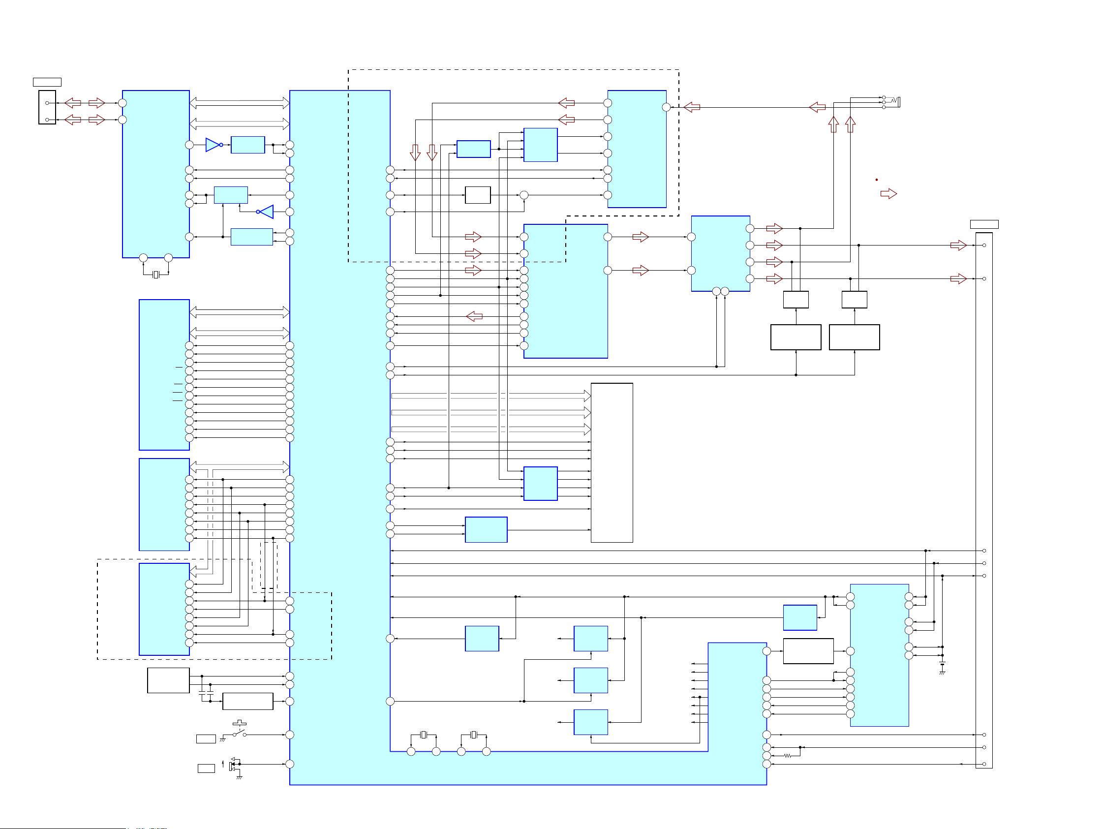
SECTION 5
DIAGRAMS
POWER CONTROL,
CHARGE CONTROL
IC901
VCC_DCIN
USB DATA0 – USB DATA15
256M bit SD-RAM
IC701
DP
A3
DM
A4
USB CONTROLLER
IC501
CD0 – CD15
SDR_DATA0 –
SDR_DATA31
SDR_A0 – SDR_A12
XINT
E3
A/D CONVERTER,
D/A CONVERTER,
HEADPHONE AMP
IC302
SYSTEM CONTROLLER, DSP, POWER CONTROLLER,
LCD DRIVER, NAND FLASH MEMORY INTERFACE,
SD-RAM INTERFACE
IC601
LEVEL SHIFT
IC509
IC507
IC508
AB0_D0 – AB0_D15
AB0_A1 – AB0_A8
USB_INT1
AC5
XCS H2 AB0_CSZ2
F22
XRD G3 AB0_RDZ
J19
XWRH F3
XWRL
H3
AB0_WRZ
H16
XRESET D1
RESETZ
P10
SDR_BA0
AB5
USB_XRST
AB13
FLASHCLK
E19
USB_INT2
AB14
SDINPM0_SO
AC22
32
11
SDA/CDINSPIO_SO
AC8
SPIO_XCS1
AB6
TU_STO
AA3
2
SCL/CCLKSPIO_SK
AC7
3
AD0/nCSSPIO_SCZ2
AD7
4
MCLKREFCLKO
U18
30
SDOUTPM0_SI
AD22
29
SCLKPM0_CLK
AC21
31
LRCKPM0_SEN
AB22
1
nRESETADA_XRST
AC20
LCD_PXCLK
P23
NC_OUT_SEL
U19
HP_XMUTE Y3
25
MUTING
Q302
CN851 (1/2)
VCC_VBUS
VCC_VBAT
VDD_UNREG
VDD_DDCOUT20
17
AU_R_OUT
14
AU_L_OUT
20
DCIN
11
USB_DET
12
UNREG_OUT
10
TXD/SLEEP
8
RXD/WAKE
9
CRD_AD
3
D+
4
D–
WM-PORT
B8
XI
C8
XO
USB ADDRESS1 – USB ADDRESS8
CA1 – CA8
DQ0 – DQ31
BA0
J7
SDR_BA1
T4BA1 H8
SDR_CLK
AA5
CLK J1
SDR_CSZ0
T3CS J8
SDR_CKE0
T1CKE J2
SDR_WEZ
R5WE K8
SDR_CASZ
U8CAS K7
SDR_RASZ
T5RAS J9
SDR_DQM0
P5DQM0 K9
SDR_DQM1
R4DQM1 K1
SDR_DQM2
R3DQM2 F8
SDR_DQM3
R2DQM3 F2
A0 – A12
SDR_D0O – SDR_D31
SDR_A00 – SDR_A12
NAND FLASH
MEMORY
IC751
NAND_DA0 –
NAND_DA7
NAND_ALE
D3
I/O1 – I/O8
ALE 17
NAND_CLE
E9CLE 16
NAND_CEZ0
M9XCE1 9
NAND_CEZ1
C2XCE2 10
NAND_CEZ2
B3
NAND_CEZ3
C3
NAND_REZ
E3XRE 8
NAND_WEZ
A4XWE 18
NAND_RBZ0
D2R/B1 7
NAND_RBZ1
H8R/B2 6
NAND_RBZ2
J8
NAND_RBZ3
K8
NAND_D0O – NAND_D07
NAND FLASH
MEMORY
IC752
I/O1 – I/O8
ALE 17
CLE
16
XCE1
9
XCE2
10
XRE
8
XWE
18
R/B1
7
R/B2
6
KEY_AD0
C6
KEY_AD1B6
EXTRST
G4
XHOLD_KEY
AD4
KEY_WAKE
AD5
D FLIP-FLOP
IC505, 506
RESET SWITCH
IC502
(NWZ-S516/S616F/S618F)
(NWZ-S516/S616F)
SHEET SWITCH
&
S888, 889
WAKE UP SWITCH
Q603
X501
12MHz
T26
CKI
U26
CKO
X603
11.2896MHz
AC26
OSCIN
AB26
OSCOUT
X602
32.768kHz
AIN2A19 COM110
COM2
6
1
AIN2B/BIAS
20
AOUT_L6
AOUT_R
5
TU_CLKON
W10
CPU_CKI32
U17
DA
7
CL
9
LA
8
STO
13
X1
10
ANT
2
SWITCHING
IC404
SWITCHING
IC405
BUFFER
Q401
+
AOUTA
2NO1
9NC1
4NO2
7NC2
10AOUTB
HEADPHONE/WM-PORT
SELECTOR
IC303
MUTING
CONTROL SWITCH
Q301
MUTING
Q303
CB15CB2
J301
(HEADPHONE)
MUTING
CONTROL SWITCH
Q304
LCD801
LIQUID
CRYSTAL
DISPLAY
R0 – R5
LCD_R0 – LCD_R5
G0 – G5
LCD_G0 – LCD_G5
B0 – B5
DOTCLK
LCD_HSYNC
K22
HSYNC
LCD_VSYNC
K24
SPIO_XCS0
AC6
LCD_PON
W3
LCD_BLTCTL
V17
BKBAT USB +1.8V
USB +3.1V
AD17
PSM_LODET
U14
LCD_PWM1
AD23
VSYNC
SDI
SCL
CS
RESET
LCD_ENABLE
K23 ENABLE
LED+
LCD_B0 – LCD_B5
LCD BACK
LIGHT DRIVER
IC803
LEVEL
SHIFT
IC802
CN851 (2/2)
WM-PORT
FM TUNER
IC403
220
3DCDC
16USB
15USB
18BAT
CHG_ICTL
17BAT
LITHIUM ION
BATTERY
3.7V 610mAh
SYS
11Y2 ISET
22 /DOK
CHG_XCHGEN
4
V10
/CEN
CHG_PEN2
6W8PEN2
USB_SUSPEND
13
AB8
USUSS
XCHG_DET
19
AC4
/CHG
CHG_XFLT
24
AB4
U70_SOUT
T17
U70_SRIN
T18
CRD_DET
AB3
CRD_AD C8
/FLT
21 SYS
DC/DC
CONVERTER
IC903
CHARGE
CONTROL SWITCH
Q903
+3.1V
REGULATOR
IC602
+1.8V
REGULATOR
IC504
+3.1V
REGULATOR
IC503
HP/WM-PORT +1.8V
+1.8V
REGULATOR
IC301
VDD_ANA_F
VDD_ECO_J
VDD_GP1_J
VDD_GP3
VDD_HP_F
VDD_LO_F
VDD_LOG_F
VDD_PLL_S
S601
RESET
S602
HOLD
OFF
ON
:AUDIO
SIGNAL PATH
(NWZ-S615F/S616F/S618F)
5-1. BLOCK DIAGRAM

NWZ-S515/S516/S615F/S616F/S618F
NWZ-S515/S516/S615F/S616F/S618F
1717
For Schematic Diagrams.
Note:
• All capacitors are in μF unless otherwise noted. (p: pF)
50 WV or less are not indicated except for electrolytics
and tantalums.
• All resistors are in Ω and 1/4 W or less unless otherwise
specif ed.
• C : panel designation.
• A : B+ Line.
• Power voltage is dc 3.7 V and fed with regulated dc power supply from CN901 pin 1 and pin 2 on the MAIN
board.
• Voltages and waveform are dc with respect to ground under no-signal conditions.
no mark : PLAY BACK
• Waveform is taken with a oscilloscope.
Voltages variation may be noted due to normal production
tolerances.
• Voltages are taken with a VOM (Input impedance 10
MΩ).
• Voltage variations may be noted due to normal production
tolerances.
• Circled number refer to waveform.
• Signal path.
F : AUDIO
L : VIDEO
• The voltage and waveform of CSP (chip size package)
cannot be measured, because its lead layout is different
form that of conventional IC.
• Abbreviation
FR : French model
THIS NOTE IS COMMON FOR PRINTED WIRING BOARDS AND SCHEMATIC DIAGRAMS.
(In addition to this, the necessary note is printed in each block.)
For Printed Wiring Boards.
Note:
• Y : parts extracted from the conductor side.
• : Pattern from the side which enables seeing.
(The other layers' patterns are not indicated.)
• MAIN board is multi-layer printed board.
However, the patterns of intermediate-layers have not
been included in diagrams.
• Indication of transistor.
Caution:
Parts face side:
(SIDE A)
Pattern face side:
(SIDE B)
Parts on the parts face side seen from
the pattern face are indicated.
Parts on the pattern face side seen from
the parts face are indicated.
• Waveform
– MAIN Board –
• Lead layouts
surface
CSP (Chip Size Package) Lead layout of conventional IC
C
Q
B
E
These are omitted.
IC903 (LX)
2 V/DIV, 500 ns/DIV
5.28 Vp-p
185 ns
NWZ-S515/S516/S615F/S616F/S618F
Ver. 1.3
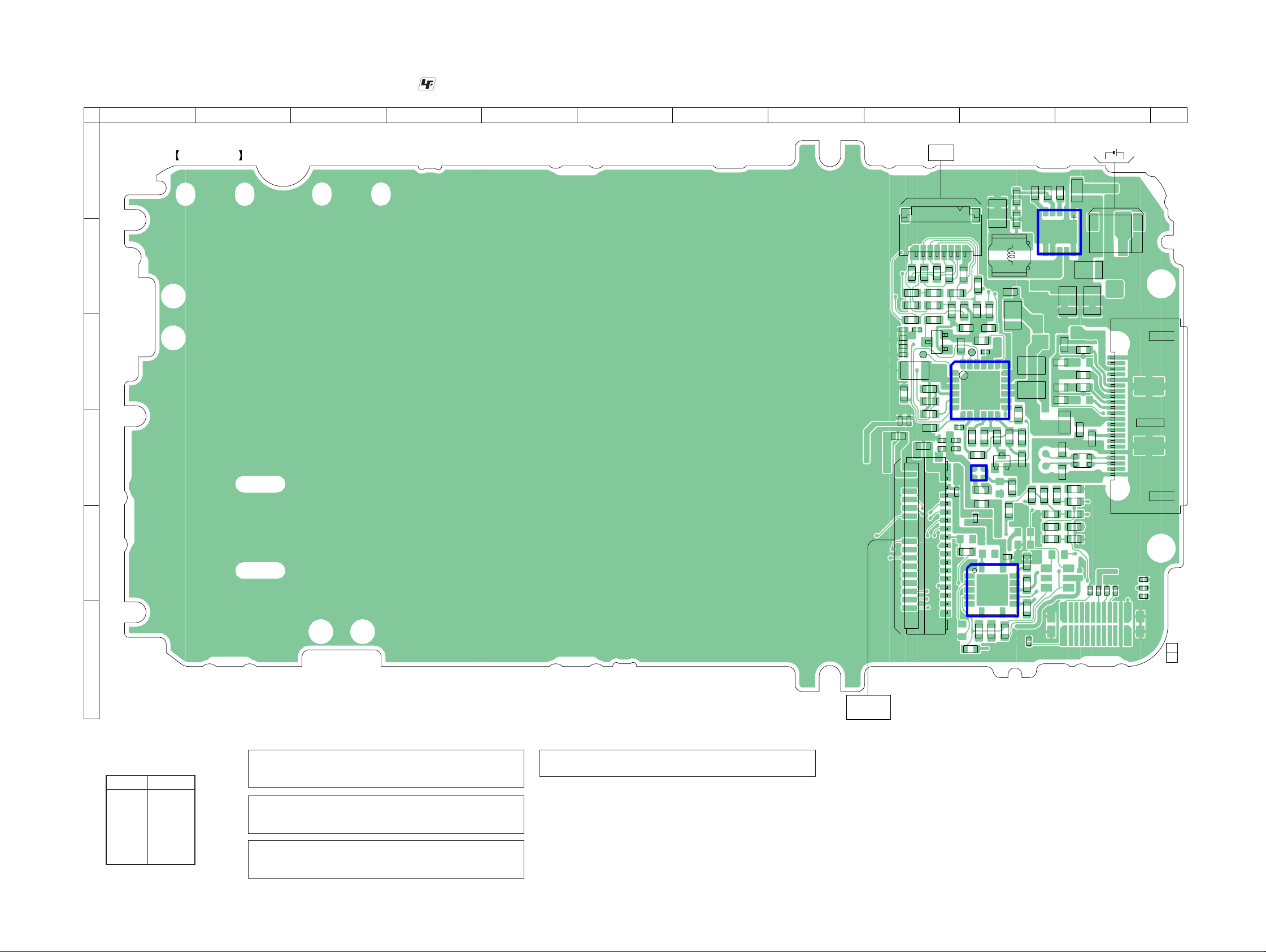
5-2. PRINTED WIRING BOARD - MAIN Board (Side A) -
123456789101112
MAIN BOARD (SIDE A)
A
B
C
D
E
F
• : Uses unleaded solder.
FB821
SHEET
SWITCH
CN881
81
81
R882
R887
R884
R885
C883
R886
C882
R665
C697
FB820
R903
C901
C612
C698
35
CL903
1
CN801
37
36
R921
R908
R904
R906
R647
S
D
G
Q603
C904
C660
C661
C618
C617
C615
C613
R883
C881
R881
C884
R648
R661
R662
R646
R649
R911
R907
CL911
24
1
25
25
IC901
6
712
C650
C651
2
C805
R833
C905
R912
A2A1
B2B1
IC602
R602
R664
C806
1
2
R909
IC802
6
34
7
R822
R828
L901
R651
C906
15
C913
VDR856
19
18
13
R919
D
GS
Q903
C802
14
8
R821
R824
R905
R855
13
R913 R914
R861
R922
R910
R672
9
R625
R915
C903
5
5
IC903
610
610
C909
VDR861
VDR859
C920
VDR860
VDR852
TH901
VDR851
VDR854
R859
C854
C853
R826
R823
R827
C911
11
VDR862
R853
FB858
FB852
FB851
R851
R857R858
1
C921
R902
241
C907
VDR858
C855
3
VDR853
C912
FB857
FB855
FB854
LF851
R626
LITHIUM ION
BATTERY
3.7V 610mAh
2
CN901
22
R637
R639
R640
112
12
1
1-874-537-
24
2625
CN851
WM-PORT
23
R636
R660
R638
11
(11)
• Semiconductor
Location
Ref. No. Location
IC602 D-10
IC802 E-10
IC901 C-10
IC903 B-11
Q603 C-9
Q903 D-10
NWZ-S515/S516/S615F/S616F/S618F
Note 1: When the MAIN board is replaced, format it according
to the “NOTE OF MAIN BOARD REPLACING” (refer to
page 4) of the servicing notes.
Note 2: When IC602, IC802, IC901 and IC903 on the MAIN board
is damaged, exchange the new MAIN board for the MAIN
board which IC damaged.
Note 3: When CN881 on the MAIN board is damaged, exchange
the new MAIN board for the MAIN board which connector
damaged.
Note 4 : When the LCD SUB ASSY (LCD801) is replaced, refer to
SUPPLEMENT-2.
1818
LCD801
LIQUID CRYSTAL
DISPLAY
NWZ-S515/S516/S615F/S616F/S618F
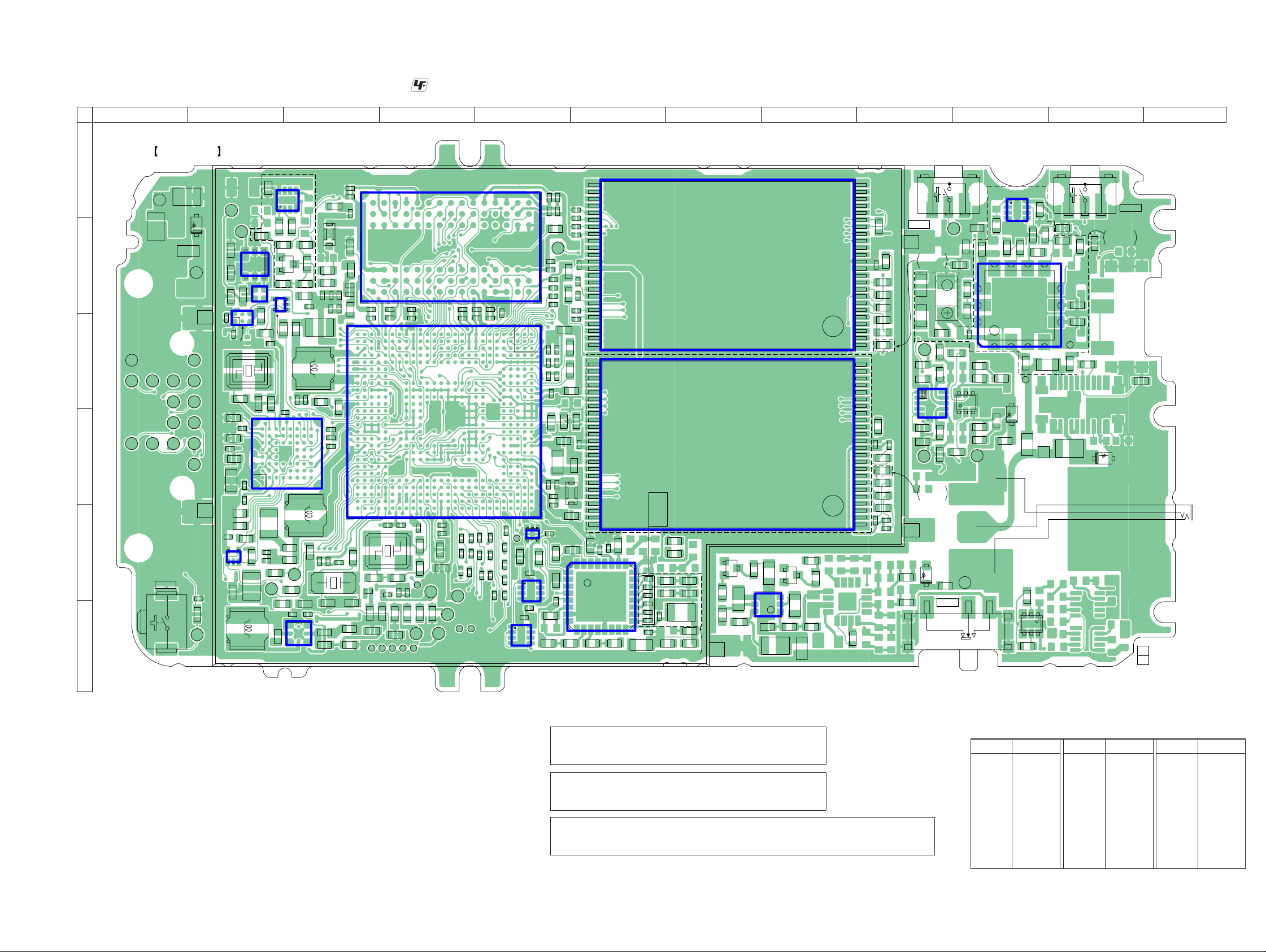
5-3. PRINTED WIRING BOARD - MAIN Board (Side B) -
123456789101112
MAIN BOARD (SIDE B)
A
R437
IC504
4
C511
C2B2
X501
C506
IC501
R519
C804
13
6
A2A1
B2B1
R520
C501
C665
C664
R510
C419
IC503
4
5
C516
R502
C644
R628
C803
IC405
8
1
154
R426
R438
Q401
S
R442
C509
CL610
R641
R820
CL901
C915
C917
R901
CL622
CL629
CL623
CL624
CL888
CL912
CL625
CL626
CL627
CL628
CL913
B
CL902
C
CL603
CL613CL614
CL604
D
E
S601
RESET
F
C611
CL646
R603
D852
CL501
C517
C518
IC509
R505
C507
R506
R507
C505
C510
5134
IC502
L801
CL502
C512
R521 R522
A1A2B1 C1
C502
C504
C503
R511
R523
R503
R832
R427
G
D
13
R616
R504
IC508
L601
L602
R617
R624
CL631
R629
A1 A3
B1
C1A2C2
IC803
(NWZ-S615F/S616F/S618F)
R605
R439
R440
R615
R653
R441
R643
C684
C695
C687
C677
C641
R839
C657
C655
C694
H8G8F8E8D8C8B8A8
H7G7F7E7D7C7B7A7
H6G6F6E6D6C6B6A6
H5G5F5C5B5A5
C508
H4G4F4C4B4A4
H3G3F3E3D3C3B3A3
H2G2F2E2D2C2B2A2
H1G1F1E1D1C1B1A1
C671
C608
X602
C626
C607
R627
R830
B3
C3
R829
FL701
C674
C610
C692
C680
R840
C691
C710
C709
C648
C647
C625
R831
C689
C634
R663
R622
C686
C629
C690
AF1
AF2
AE3AF3
AF10
AF12
AF19
AE19
AF23
AE24AF24
AE25AF25
AF26
R611
C616
AD7
AD8
AD10
AD20
AD21
AD22
AD23
C666
R642
CL643
AD3
AD4
AD5
AD6
AD9
AD11
AD12
AD13
AD14
AD15
AD16
AD17
AD18
AD19
AD24
C668
C640
AC5AE5AF5
AC6AE6AF6
AC7AE7AF7
AC8AE8AF8
AC9AE9AF9
AC10AE10
AC11AE11AF11
AC12AE12
AC13AE13AF13
AC14AE14AF14
AC15AE15AF15
AC16AE16AF16
AC17AE17AF17
AC18AE18AF18
AC19
AC20AE20AF20
AC22AE22AF22
CL620
• : Uses unleaded solder.
IC701
C707
C713
C652
C679
C708
W1 G1 F1
AB1AC1AD1AE1
AB2AC2AD2AE2
AB3AC3
AB4AC4AE4AF4
AB5
AB6
AB7
AB8
AB9
AB10
W11
V11
AB11
W12
V12
AB12
W13
V13
AB13
W14
V14
AB14
W15
V15
AB15
W16
V16
AB16
AB17
AB18
AB19
AB20
AB21
AC21AE21AF21
AA22AB22
AA23AB23AC23AE23
AA24AB24AC24
AA25AB25AC25AD25
AA26AB26AC26AD26AE26
C667
X603
R633
C675
C672
C699
C602
C603
C606
C638
CL638
CL634
C653
C714
R4T4U4V4W4 G4 F4 C4
U11
U12
U13
U14
U15
U16
CL642
CL637
C620
C669
R634
C604
CL644
IC601
C670
FB801
C643
CL641
C601
CL914
H10J10K10L10M10N10P10R10T10U10V10W10
K11
J11
H11
L11 D11 B 11 A 11
K12
J12
H12
K13
J13
H13
K14
J14
H14
K15
J15
H15
K16
J16
H16
J17K17 H17L17M17N17P17R17T17U17V17W17
J18K18 H18L18M18N18P18R18T18U18V18W18
J19K19 H19L19M19N19P19R19T19U19V19W19
J22K22 H22L22M22N22P22R22T22U22V22W22 G22 F22 E22Y22
H23
J23K23
L23M23N23P23R23T23U23V23W23 G23 F23 E23 D23 B23 A23Y23
H24J24K24L24M24N24P24R24T24U24V24W24 G24 F24 E24 D24Y24
H25J25K25L25M25N25P25R25T25U25V25W25 G25 F25 E25 D25 C25 B25 A25Y25
H26
J26K26L26M26N26P26R26T26U26V26W26 G26 F26 E26 D26 C26 B26 A26Y26
C673
FB806
FB807
FB809
FB805
FB803
FB804
FB802
CL915
CL645
CL639
CL633
C676
H1J1K1L1M1N1P1R1T1 E1U1V1 D1 C1 B1 A1Y1AA1
H2J2K2L2M2N2P2R2T2U2V2W2 G2 F2 D2 C2 B2 A2Y2AA2
H4J4K4L4M4N4P4
H5J5K5L5M5N5P5R5T5U5V5W5 G5 F5
H8J8K8L8M8N8P8R8T8U8V8W8
H9J9K9L9M9N9P9R9T9U9V9W9
FB810
FB808
FB811
FB812
C712
C711
FB818
CL640
FB813
FB814
E2
E3H3J3K3L3M3N3P3R3T3U3V3W3 G3 F3 D3Y3AA3
E4 D4 B4 A4Y4AA4
E5Y5AA5
E6
E7
E8
E9
E10
E11
E12
E13
E14
E15
E16
E17
E18
E19
E20
E21
FB816
R658
C3
D5 B5 A5
C5
C6
D6 B6 A6
C7
D7 B7
C8
D8 B8 A8
C9
D9 B9 A9
C10
D10 B10
C11
C12
D12 B12
C13
D13 B13 A13
C14
D14 B14 A14
C15
D15 B15 A15
C16
D16 B16 A16
C17
D17 B17 A17
C18
D18 B18 A18
C19
B19
D19 A19
C20
D20
B20 A20
C21
D21 B21 A21
C22
D22 B22 A22
C23
C24
B24 A24
FB819
R516
FB817
IC506
FB815
1
1
4
IC505
B3 A3
1
A1B1C1D1E1F1G1H1J1K1L1M1N1P1R1
A2B2C2D2E2F2G2H2J2K2L2M2N2P2R2
A3B3C3D3E3F3G3H3J3K3L3M3N3P3R3
A7B7C7D7E7F7G7H7J7K7L7M7N7P7R7
A8B8C8D8E8F8G8H8J8K8L8M8N8P8R8
A9B9C9D9E9F9G9H9J9K9L9M9N9P9R9
A10
A12
8
5
A7
13
54
C514
8
54
R513
C513
C701
C704
R702
CL890
C633
R656
R657
C681
C688
C646
C645
C662
C682
C656
C654
IC507
C515
R514
C308
R205
C705
C678
R775
R780
R644
R608
R314
C301
C702
C706
R781
C649
C632
C703
R655
C685
R618
R630
C683
R623
C306
C207
R774
R776
R777
R604
R621
R620
R619
FB601
C755
VDR302
R315
1
8
R607
FL601
32
9
C753
R778
R779
IC302
C107
C302
C303
R313
24
S888
VOL -
R107
R207
NWZ-S516/
S616F
R432
C417
CL101
C113
C322
5
IC303
R319
C213
CL201
NWZ-S516/
S616F
D201
CL891
FB418
1
R115
R121
10
6
R221
R215
FB201
S602
HOLD
R447
R321
FB602
C411
R670
C412
R208
Q302
1
R108
CL202
U
ONOFF
R769
C752
R754
R783
R753
R756
R755
R782
1
R752
24
R751
C754
R759
R761
R762
R760
R758
R757
R767
1
R765
R764
C325
R446
46
3
CL102
C110
C109
C209
C210
R417
FB425
12
14
11
11
1
R110
R210
FB101
IC404
1
9
4
FB435
R419
IC403
D101
8
5
C413
R434
C414
CL402
R320
R109
3
46
Q303
R209
S889
R422
D301
1-874-537-
VOL +
NWZ-S615F/
S616F/S618F
R667
J301
(HEADPHONE)
11
(11)
C418
R424
R420
VDR401
FB421
8
8
7
7
R445
5
5
4
CL302
1
R311
R444
CL403
VDR301
R668
FB301
4
25
IC751
48
25
IC752
C104
C204
C205
C105
C206
VDR303
25
24
17
16
R326
(NWZ-S615F/S616F/S618F)
C106
C310
C313
C201
C101
C315
R324
FB325
C312
R201
R101
C311
C314
Q301
R306
R312
(NWZ-S516/S616F/S618F)
C321
R307
4
6
IC301
C316
C319
Q304
E
3
C305
1
R304R305
R302
R325
E
C307
R310
48
R105
NWZ-S515/S516/S615F/S616F/S618F
Note 1: When the MAIN board is replaced, format it according
to the “NOTE OF MAIN BOARD REPLACING” (refer to
page 4) of the servicing notes.
Note 2: When C104 and C204 on the MAIN board is damaged,
exchange the new MAIN board for the MAIN board which
capacitor damaged.
Note 3: When IC301, IC302, IC303, IC404, IC405, IC501, IC503, IC505, IC506, IC507,
IC508, IC509, IC601, IC701, IC751, IC752 and IC803 on the MAIN board is damaged, exchange the new MAIN board for the MAIN board which IC damaged.
1919
• Semiconductor Location
Ref. No. Location
D101 D-10
D201 E-9
D301 D-11
D852 B-2
IC301 F-8
IC302 E-6
IC303 C-9
IC403 B-10
IC404 A-10
IC405 A-3
Ref. No. Location Ref. No. Location
IC501 D-3
IC502 E-2
IC503 B-2
IC504 B-2
IC505 F-5
IC506 E-5
IC507 E-5
IC508 B-2
IC509 C-2
IC601 D-4
IC701 B-4
IC751 B-7
IC752 D-7
IC803 F-3
Q301 E-7
Q302 C-10
Q303 F-10
Q304 E-8
Q401 B-3

NWZ-S515/S516/S615F/S616F/S618F
NWZ-S515/S516/S615F/S616F/S618F
2020
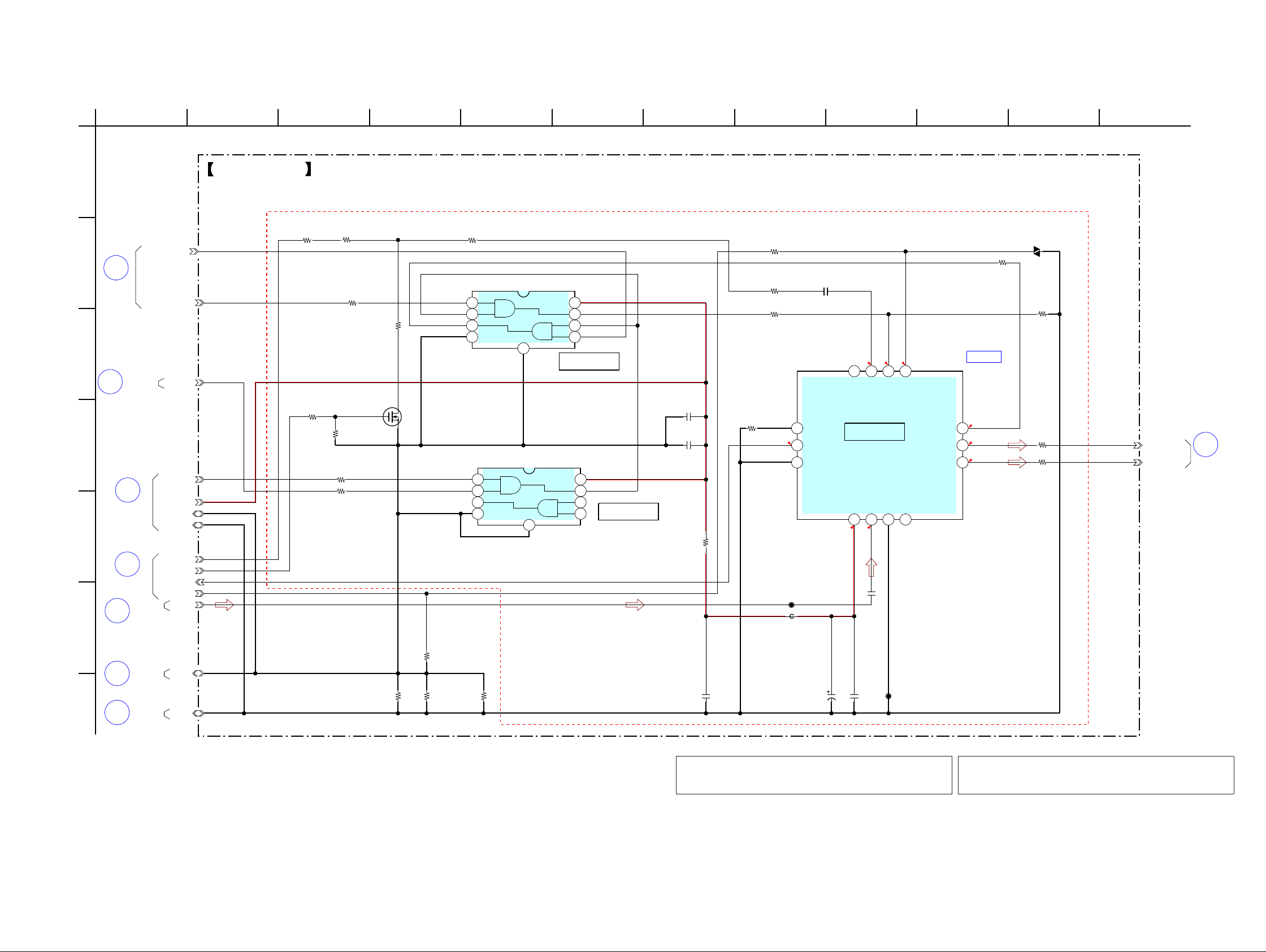
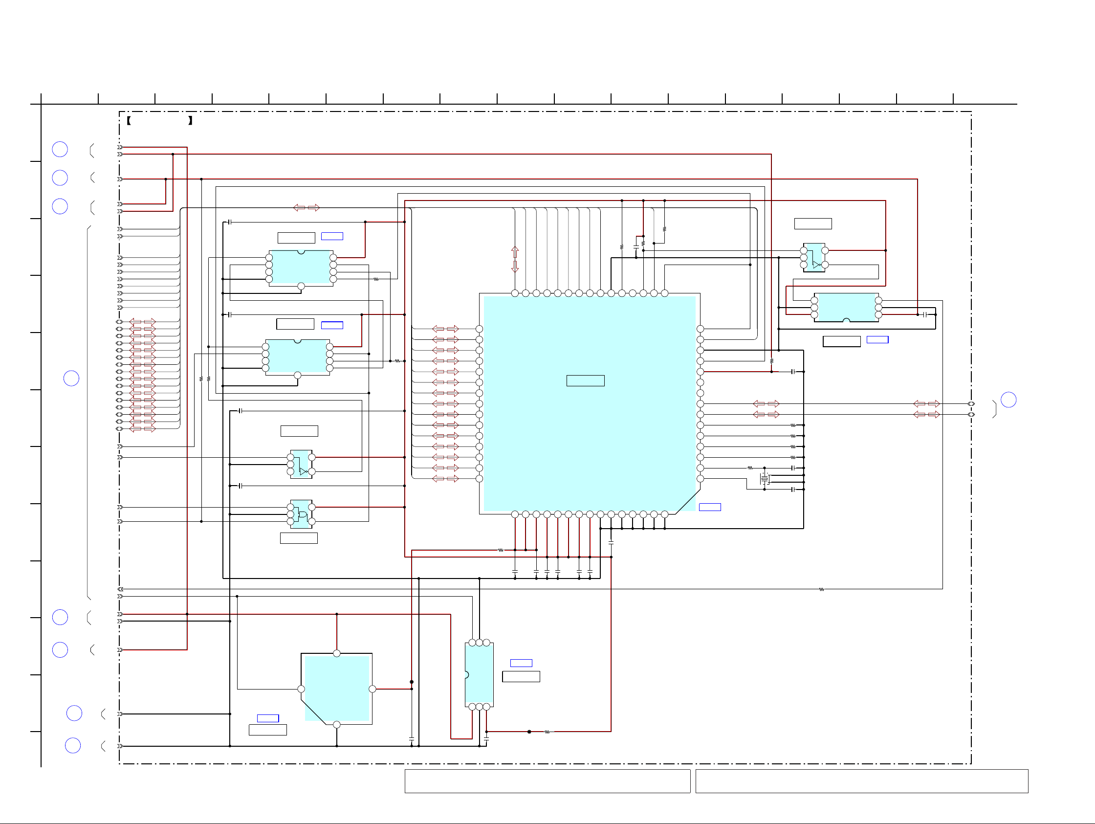
5-4. SCHEMATIC DIAGRAM - MAIN Board (1/10) -
• See page 30 for IC Block Diagrams. • See page 33 for IC Pin Function Description.
BOARD
MAIN
(4/10)
9
BOARD
MAIN
(2/10)
12
BOARD
MAIN
(2/10)
8
BOARD
MAIN
(7/10)
7
BOARD
MAIN
(4/10)
6
BOARD
MAIN
(2/10)
5
BOARD
MAIN
(4/10)
2
BOARD
1
(4/10)
MAIN
BOARD
3
(10/10)
MAIN
13
(8/10)
MAIN
BOARD
BOARD
14
(2/10)
MAIN
IC B/D
IC B/D
00
0.3
0
0
0.3
0
0
IC302
∗
12345 678
9
10
11
12
13
14
15
16
1718192021222324
25
26
27
28
29
30
31
32
33
VDD_HP_F
C308
1
C311
1
C314
1
ADA_XRST
PCM0_DADT
CPU_REFCLKO
R105
47
R205
47
C107 0.068
SPI0_MOSI
SPI0_CLK
SPI0_XCS2
DGND
AGND
C303 0.1
VDD_DDCOUT20
C310 0.1
C315
1
C313
0.1
C205
0.001
C306
0.1
C110
0.22
R110
2.2
R210
2.2
C210
0.22
C207 0.068
C105
0.001
C104
150p
C204
150p
C301
0.001
C206
0.001
C106
0.001
R108
470
R209
470
R208
470
R109
470
C302
0.1
LINE_OUT_R
LINE_OUT_L
HP_XMUTE
C312
22
CRD_LINEOUT
D101
RSB6.8STE61
D201 RSB6.8STE61
Q302
EMX18
6
2
1
3
5
4
Q303
EMX18
6
2
1
3
5
4
R307
1k
Q301
UNR31A600LS0
R305
220k
C305
10
IC301
XC6401FF58DR
123
456
7
C316
22
C307
10
R310
0
R312
0
R306
0
R302
0
C319
4.7
R313
1k
C321
0.022
Q304
UNR31A600LS0
R304
150k
R314
0R315
220
CL101
CL201
PCM0_BCK
PCM0_ADDT
FB201
FB301
FB101
VDR301
PCM0_LRCK
0
R311
TU_ANT
0.068
C101
0.068
C201
0R101
0R201
TU_OUT_L
TU_OUT_R
100p
C209
100p
C109
MAX4745ELB+TB069
IC303
1
CB12NO13GND4NO25CB2
6
COM2
7
NC2
8
VCC
9
NC1
10
COM1
0.1C322
R215
0
R121
470
R115
0
R221
470
R319
0
VDR302
VDR303
R107
∗
R207
∗
C113
0.0047
C213
0.0047
VDD_HP_F
R320
0
D301
RSB6.8STE61
470k
R321
CL302
J301
0
R324
SPI0_MOSI_1
SPI0_CLK_1
1
C325
CL102
CL202
0
R325
0
R326
FB325
0
SPI0_XCS2
VDD_DDCOUT20
SPI0_CLK
SPI0_MOSI
LRCK
SDA/CDIN
SCL/CCLK
AD0/nCS
VA_HP
FLYP
GND_HP
FLYN
ADC_FILT+
VQ
DAC_FILT+
AGND
VA
AOUTA
AOUTB
VSS_HP
AIN1B
AIN1A
AFILTB
AFILTA
AIN2B/BIAS
AIN2A
MICIN2/AIN3B/BIAS
MICIN1/AIN3A
nRESET
VL
VD
DGND
SDOUT
MCLK
SCLK
SDIN
AGND
D/A CONVERTER
EN1
GND
VOUT2
VOUT1
VSS
EN2
VIN
(1/10)MAIN BOARD
HEADPHONE/WM-PORT
IC303
+1.8V REGULATOR
IC301
A/D CONVERTER,
IC302
A
1012
J
H
B
1311
L
C
78
I
14
F
96
K
4 1815 163
G
D
5 17
E
12
HEADPHONE AMP
NWZ-S615F/
S616F/F618F
()
()
S616F/F618F
NWZ-S615F/
S616F/F618F
()
NWZ-S615F/
MUTING CONTROL SWITCH
MUTING CONTROL SWITCH
∗
IC302
CS42L51-CNZR
(NWZ-S615F/S616F/S618F)
(NWZ-S515/S516)
CS43L21-CNZR
51(FR)
∗
R107,207
5.6(EXCEPT FR)
SELECTOR
MUTING
MUTING
(HEADPHONE)
)
NWZ-S615F/
(
S616F/F618F
(Page 23)
(Page 23)
(Page 29)
(Page 21)
(Page 23)
(Page 26)
(Page 21)
(Page 23)
(Page 27)
(Page
21)
(Page 21)
Note 2: When C104 and C204 on the MAIN board is damaged,
exchange the new MAIN board for the MAIN board which
capacitor damaged.
Note 3: When IC301, IC302 and IC303 on the MAIN board is
damaged, exchange the new MAIN board for the MAIN
board which IC damaged.
Note 1: When the MAIN board is replaced, format it according
to the “NOTE OF MAIN BOARD REPLACING” (refer to
page 4) of the servicing notes.
NWZ-S515/S516/S615F/S616F/S618F
NWZ-S515/S516/S615F/S616F/S618F
2121
5-5. SCHEMATIC DIAGRAM - MAIN Board (2/10) -
• See page 30 for IC Block Diagrams.
BOARD
(1/10)
MAIN
12
BOARD
(1/10)
MAIN
8
BOARD
(4/10)
MAIN
15
BOARD
(4/10)
MAIN
16
BOARD
(1/10)
MAIN
5
36
MAIN
(7/10)
BOARD
MAIN
4
(3/10)
BOARD
(1/10)
14
BOARD
MAIN
IC B/D
0
2.9
0
2.9
0
0
0
2.8
2.8
SPI0_MOSI_1
SPI0_XCS1
SPI0_CLK_1
VDD_HP_F
TU_OUT_R
TU_OUT_L
68
R417
1k
R419
SDFMM1N23GB2T
IC403
1
Vcc2ANT3GND4RSSO
5
AOUT_R
6
AOUT_L
7
DA
8
LA
9CL10X111
X2
12
D_GND
13
STO
14
GND
0.1
C413
CPU_CKI32
TU_CLKON
220p
C414
0.1
C412
TU_ANT
CL402
CL403
AGND
VDR401
DGND
1k
R420
10V
47
C411
R422
0
TC7WH08FC(T5RSONY)
IC404
1
2
3
4
GND
5
6
7
8
VCC
9
GND
TC7WH08FC(T5RSONY)
IC405
1
2
3
4
GND
5
6
7
8
VCC
9
GND
SPI0_XCS2
SPI0_XCS0
1
C417
0.1
C419
0.1
C418
R426
0
R427
0
4700
R434
2SK354700LS0
Q401
470k
R437
R438
0
6800
R441
4700
R440
R442
0
R439
0
0
R444
0
R445
FB418
0
R446
0
R447
R432
0
FB421
0
FB425
0
FB435
0
TU_STO
220k
R424
DGND
AGND
MAIN BOARD (2/10)
IC405
SWITCHING
IC404
SWITCHING
FM TUNER
IC403
A
1012
B
11
C
78
F
9643
G
D
5
E
12
S
BUFFER
(NWZ-S615F/S616F/S618F)
(Page 20)
(Page 26)
(Page 20)
(Page 23)
(Page 20)
(Page 22)
(Page 23)
(Page 20)
Note 2: When IC404 and IC405 on the MAIN board is damaged,
exchange the new MAIN board for the MAIN board which
IC damaged.
Note 1: When the MAIN board is replaced, format it according
to the “NOTE OF MAIN BOARD REPLACING” (refer to
page 4) of the servicing notes.
NWZ-S515/S516/S615F/S616F/S618F
NWZ-S515/S516/S615F/S616F/S618F
2222
5-6. SCHEMATIC DIAGRAM - MAIN Board (3/10) -
• See page 30 for IC Block Diagrams.
(8/10)
23
MAIN
BOARD
(7/10)
21
MAIN
BOARD
(4/10)
42
MAIN
BOARD
(4/10)
17
MAIN
BOARD
BOARD
MAIN
(4/10)
18
BOARD
MAIN
(10/10)
19
MAIN
4
(2/10)
BOARD
MAIN
22
(10/10)
BOARD
BOARD
MAIN
20
(4/10)
IC B/D
IC B/D
IC B/D
IC B/D
IC B/D
IC B/D
IC501
CSP
(Chip Size Package)
S1R72V17B00A20B
B8
XI
C8
XO
H1
TESTEN
H8
ATPGEN
A8
BURNIN
A6
R1
A3
DP
A4
DM
B1
VBUSFLG
C1
VBUSEN
C3
VBUS
D1
XRESET
D8
CLKIN
G3
XRD
H3
XWRL
F3
XWRH
H2
XCS
E3
XINT
G4
XDREQ
F4
XDACK
D2
XBEL
C4
CA1E1CA2C5CA3E2CA4D3CA5G1CA6F1CA7F2CA8
H4
CD0
G5
CD1
H5
CD2
F5
CD3
E6
CD4
H6
CD5
G6
CD6
F6
CD7
H7
CD8
G8
CD9
F7
CD10
E7
CD11
F8
CD12
D6
CD13
E8
CD14
C6
CD15
A5
HVDDB3HVDDC2HVDDA2LVDDA7LVDDC7LVDDG2LVDDD7CVDDB2VSSB4VSSB5VSSB6VSSB7VSSG7VSSA1NSS(NC)
X501
12MHz
C502
15p
DGND
R502
0
C501
18p
R507
1k
C503
1
R503
100k
R504
100k
R505 100k
R506
6200
AB0_XRD
AB0_XWR
AB0_XCS2
AB0_D1
AB0_D0
AB0_D3
AB0_D2
AB0_D7
AB0_D6
AB0_D5
AB0_D4
AB0_D10
AB0_D8
AB0_D9
AB0_D11
AB0_D15
AB0_D12
AB0_D14
AB0_D13
AB0_A1
AB0_A2
AB0_A3
AB0_A4
AB0_A7
AB0_A6
AB0_A5
AB0_A8
USB_INT
VDD_GP1_J
IC503
TK63731AB1G0B
A1
GND
B1
VOUT
B2
VIN
A2
VCONT
PSM_L0DET
VDD_UNREG
C504
0.1
C511
1
R511
220k
RESETZ
C510
0.1
USB_DP
USB_DM
VCC_VBUS
C512
1
C505
0.1
C506
0.1
C507
0.1
C509
0.1
C508
0.1
IC505
TC7WG74FC
1
CK
2
D
3
/Q
4
GND
5
Q
6
/CLR
7
/PR
8
VCC
9
GND
C513
0.1
FLASHCLK
R513
100k
IC506
TC7WG74FC
1
CK
2
D
3
/Q
4
GND
5
Q
6
/CLR
7
/PR
8
VCC
9
GND
C514
0.1
IC507
TC7SG04AFS
12
GND
3
NC
45
VCC
C515
0.1
R516
10
R514
10
USB_XRST
R519
220k
IC502
TC7SG08AFS
12
GND
3
45
VCC
IC504
TK63718HCL-G
1
VIN2GND3VOUT
4NC5
GND
6
VCONT
IC508
TC7SG04AFS
1
2
GND
3
NC
4
5
VCC
C516
0.1
C517
0.1
C518
0.1
R510
22
IC509
SN74AVC1T45YZPR
A1
VCCA
B1
GND
C1
A
C2
B
B2
DIR
A2
VCCB
R520 100k
R521
0
R522
0
10k
R523
CL501
CL502
VCC_VBUS
VDD_GP1_J
VDD_UNREG
VDD_UNREG
DGND
DGND
AB0_XRD
AB0_A2
AB0_A3
AB0_A4
AB0_A5
AB0_A6
AB0_A7
AB0_A8
AB0_D0
AB0_D1
AB0_D2
AB0_D3
AB0_D4
AB0_D5
AB0_D6
AB0_D7
AB0_D8
AB0_D9
AB0_D10
AB0_D11
AB0_D12
AB0_D13
AB0_D14
AB0_D15
AB0_A1
AB0_XRD
AB0_D0
AB0_A8
AB0_A7
AB0_A6
AB0_A5
AB0_A4
AB0_A3
AB0_A2
AB0_A1
AB0_D1
AB0_D2
AB0_D3
AB0_D4
AB0_D5
AB0_D6
AB0_D7
AB0_D8
AB0_D9
AB0_D10
AB0_D11
AB0_D12
AB0_D13
AB0_D14
AB0_D15
AB0_XCS2
AB0_XCS2
USB CONTROLLER
IC501
+1.8V REGULATOR
IC504
+3.1 REGULATOR
IC503
RESET SWITCH
IC502
IC507
INVERTER
IC505
D FLIP-FLOP
IC506
D FLIP-FLOP
IC508
INVERTER
IC509
LEVEL SHIFT
CSP
(Chip Size Package)
MAIN BOARD
A
1012
J
H
B
1311
C
78
I
14
F
96
K
4 15 163
G
D
5 17
E
12
(3/10)
L
(Page 23)
(Page 23)
(Page 29)
(Page 23)
(Page 26)
(Page 29)
(Page 21)
(Page 23)
(Page 27)
Note 2: When IC501, IC503, IC505, IC506, IC507, IC508 and IC509 on the MAIN board is
damaged, exchange the new MAIN board for the MAIN board which IC damaged.
Note 1: When the MAIN board is replaced, format it according to the “NOTE OF
MAIN BOARD REPLACING” (refer to page 4) of the servicing notes.
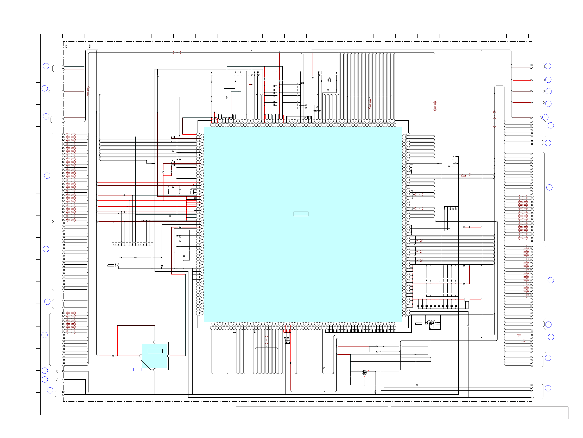
NWZ-S515/S516/S615F/S616F/S618F
NWZ-S515/S516/S615F/S616F/S618F
2323
5-7. SCHEMATIC DIAGRAM - MAIN Board (4/10) -
• See page 30 for IC Block Diagrams. • See page 33 for IC Pin Function Description.
28
MAIN
BOARD
(6/10)
27
MAIN
BOARD
(8/10)
25
MAIN
BOARD
(5/10)
17
MAIN
BOARD
(3/10)
30
MAIN
BOARD
(7/10)
BOARD
MAIN
24
(8/10)
(1/10)
BOARD
2
MAIN
BOARD
MAIN
26
(5/10)
BOARD
MAIN
29
(8/10)
MAIN
16
BOARD
(2/10)
42
(3/10)
BOARD
MAIN
BOARD
MAIN
9
(1/10)
BOARD
MAIN
18
(3/10)
BOARD
MAIN
32
(6/10)
MAIN
(10/10)
BOARD
33
34
BOARD
(8/10)
MAIN
BOARD
MAIN
20
(3/10)
BOARD
MAIN
35
(7/10)
BOARD
MAIN
6
(1/10)
BOARD
MAIN
1
(1/10)
BOARD
MAIN
15
(2/10)
BOARD
MAIN
36
(9/10)
31
(5/10)
BOARD
MAIN
IC B/D
2.9 0
2.7
LCD_R5
LCD_R4
LCD_R3
LCD_R2
LCD_R1
LCD_R0
LCD_G5
LCD_G3
LCD_G4
LCD_G1
LCD_G0
LCD_G2
LCD_B5
LCD_B3
LCD_B4
LCD_B2
LCD_B0
LCD_B1
LCD_PXCLK
LCD_HSYNC
LCD_VSYNC
SDR_D14
SDR_D27
SDR_D29
SDR_D09
SDR_D24
SDR_D23
SDR_D20
SDR_D22
SDR_D00
SDR_D21
SDR_D28
SDR_D06
SDR_D18
SDR_D16
SDR_D01
SDR_D04
SDR_D03
SDR_D31
SDR_D25
SDR_D05
SDR_D07
SDR_D26
SDR_D10
SDR_D19
SDR_D11
SDR_D30
SDR_D13
SDR_D02
SDR_D17
SDR_D08
SDR_D12
SDR_D15
SDR_XRAS
SDR_A10
SDR_A11
SDR_XWR
SDR_XCAS
SDR_A07
SDR_DQM2
SDR_DQM3
SDR_A05
SDR_A04
SDR_A06
SDR_CLK
SDR_BA1
SDR_A01
SDR_A08
SDR_A03
SDR_A00
SDR_DQM0
SDR_A09
SDR_BA0
SDR_A02
SDR_XCS0
SDR_DQM1
SDR_CKE0
SDR_A12
CPU_REFCLKO
PCM0_DADT
ADA_XRST
SPI0_XCS2
R634
1M
X603
11.2896MHz
C669
5p
C668
5p
R633
0
C646
0.1
C648
0.1
C656 0.1
DGND
C650 0.001
C651
0.1
C666
0.1
C664 0.1
C661
0.1
C671
0.001
C676
0.001
C670
0.001
C657 0.001
C672
0.001
C667
0.001
C649
0.001
C660
0.001
C654
0.1
C674
0.1
C680
0.1
C687
0.1
C675
0.1
C688
0.1
C690
0.1
C683
0.1
C679
0.1
C673
0.1
C652
0.1
C695 0.1
C694
0.1
C611
0.001
C626
10p
C625 10p
C689
0.047
R642
100k
C645
0.1
C638
1
C633
0.1
C634
0.1
C617 0.1
AGND
C615
0.1
C618
0.1
C608
1
C616
0.1
C640 1
C629
1
R616
0.22
C610
0.1
R617
0.22
C604
1
C601
1
VCC_VBUS
C613
0.1
C612
0.1
VDD_DDCOUT20
Q603
3LP01S-K-TL-E
R646
470k
R647
470k
R649
47k
C620
0.1
R639
47k
R638
47k
R640
47k
R627
1k
R625
100k
R626
100k
CRD_AD
C602
1
VDD_GP1_J
CRD_LINEOUT
VCC_VBAT
R611
0
C692
0.001
C677 0.001
C684
0.001
C691
0.001
C678
0.001
C681
0.1
C685
0.001
C686
0.001
C682
0.001
C698
0.1
C697
0.001
C647
0.001
C665
0.001
C655
0.001
C653
0.001
CHG_PEN2
CHG_XCHGEN
USB_SUSPEND
X602
32.768kHz
C603
1
R608
1k
R607
470k
C632
1
R604
0
R605
0
C607
1
VDD_HP_F
VDD_ECO_J
R643
0
R644
0
R630
100
R624
0
R623
0
R622
0
R618
0
R651
470k
R615 1k
C641
22
C644
22
VDD_UNREG
CL620
R648
47k
R621 0
R619
0
R603
10k
R629
470k
R628
470k
R641 1k
CRD_DET
R620
0
R653
100k
R657
100k
R658
100k
R656
100k
R655
100k
C643
1
LCD_PWM1
LCD_PCI
LCD_PON
HP_XMUTE
CHG_XFLT
XCHG_DET
CL633
CL634
VCC_DCIN
CL637
R660
47k
R637
47k
R636
47k
CHG_ICTL
C662
0.001
VDD_LOG_F
L601
10uH
L602
10uH
RESETZ
AB0_D0
USB_INT
AB0_XCS2
AB0_XRD
AB0_A1
AB0_A4
AB0_A3
AB0_XWR
AB0_A2
AB0_A6
AB0_A5
AB0_A8
AB0_D1
AB0_D2
AB0_D3
AB0_D7
AB0_D6
AB0_D4
AB0_D5
AB0_D9
AB0_D8
AB0_D10
AB0_D11
AB0_D15
AB0_D13
AB0_D12
AB0_D14
AB0_A7
CL603
CL604
CL610
CL613
CL614
CL622
CL623
CL624
CL625
CL626
CL627
CL628
CL629
CL631
FLASHCLK
USB_XRST
PCM0_ADDT
PCM0_BCK
PSM_L0DET
TK63731AB1G0B
IC602
A1
GND
B1
VOUT
B2
VIN
A2
VCONT
0
R602
PCM0_LRCK
SPI0_MOSI
SPI0_CLK
SPI0_XCS1
CPU_CKI32
TU_CLKON
TU_STO
VDD_GP3
470k
R661
KEY_AD0
KEY_AD1
SPI0_XCS0
1k
R662
KEY_WAKE0
CL638
CL639
CL640
CL642
LCD_ENABLE
R663
100k
0
R664
0.1
C699
C606
1
CL643
VDD_ANA_F
LCD_BLTCTL
S602
1kR665
470k
R667
100k
R668
FL601
CL641
CL644
CL645
CL646
220k
R670
0
R672
FB602
IC601
CSP
(Chip Size Package)
MC-10051F1-FAE-A
H18
C21
D21
E21
A22
B22
C22
D22
A23
B23
C23
H19
D23
B24
E23
C24
F23
E24
D18
E18
C20
D20
E20
A21
B21
H15
J18
K19
H17
E22
F22
G22
D24
C25
J22
J23
J24
G25
G24
G23
D25
F24
E25
F25
H25
H24
H22
H23
J19
H14
H16
E19
AC15
AD15
AE15
AC14
AD14
AE14
AB12
AD12
AB14
AB13
AC12
AE11
AD11
AC11
AB11
AE10
AD10
AC10
AB10
V22
U24
W23
U22
T24
V23
U19
W22
V18
V17
V19
AE16
D8
J11
J12
J13
J14
J15
J16
J17
K10
K11
K12
K13
K14
K15
K16
K17
K18
L10
L17
L18
M10
M17
M18
N10
N17
N18
N19
N9
P17
P18
P19
P9
R19
R9
T19
T9
U9
V12
V13
V14
V15
V9
W1
1
W12
W13
W14
W15
W16
W17
W18
W9
U13
U12
AD24
AC19
AD19
A19
AC1
AC2
AC3
AD18
AE19
B19
C19
D19
J1
J2
J3
P25
P26
V1
V2
V3
A5
AE13
B5
C5
D5
E5
F5
W24
W25
AB9
AC25
AC9
AD9
AE9
M19
L19
L22
L23
L24
L25
K23
M22
M23
M24
M25
N22
N23
K22
P23
N24
N25
R22
P22
R23
T22
K24
AC17
AB17
AC16
AB16
AB15
AB18
AC18
U10
V11
R10
U11
T10
D3
M9
C2
B3
C3
E9
B4
C4
H9
H10
J10
H11
H12
H13
D4
E4
L9
E6
K9
E8
E7
J9
D2
H8
J8
K8
E3
A4
AC21
AB22
AD22
AC22
AB21
AB20
AD20
AC20
AC23
AD23
V16
U16
U14
U15
P10
AA4
Y5
U3
U2
U1
Y4
W5
W4
V5
V4
V8
U5
U4
AB5
T4
U8
T1
T8
AA5
T3
T2
R1
R8
N3
N2
N1
M8M5M4
M3
M2
M1
L8
P4
L4
L3
L2
L1
L5
H3
K5
H4
K4
J4
P3
J5
H5
P2
P1
P8
N8
N5
N4
P5
R4
R3
R2
T5
R5
AC6
AB6
AD7
AB7
AC7
AC8
W10
AB8
V10W8U17
U26
T26
AB19
W19
U18
Y23
Y22
AA24
AB24
AA23
AB23
AA22
R17
R18
T17
T18
C13
C10
D12
C12
D13
B14
C14
D14
E14
C11
D10
D11
AE18
Y24
Y25
A20
AB1
AE7
B20
R25
AD8
AE8
D6
D7
K1
K2
K3
C9
C6
B6
C7
B7
C8
B8
AD6
B9
L26
K26
H26
J25
K25
G26
J26
D26
E26
F26
H2
AF19
AF12
AF13
AE12
AF16
AF17
AF14
AF15
AE17
AF18
AE5
AF10
AF11
AE6
AF5
AF6
AF8
AF9
AF7
AE3
AF4
AE4
AD5
AD4
AA2
AA1
Y3
Y2
W2
W3
AD3
AD2
AC5
AC4
AB4
AB3
AB2
AA3
F1
G1
W1
Y1
E10
E13
E12
C16
D16
C15
B15
E11
B13
E15
D15
B17
C17
D17
A17
AF21
AB25
AD21
AD25
R24
AA26
AA25
V26
V25
AF20
AE20
AF22
AE21
AF23
AE22
AE24
AE23
Y26
W26
AC24
T25
U23
M26
N26
U25
V24
G4
G5
AD17
AB26
AC26
AC13
AD16
AD13
F2
E1
P24
F4
D1
G3
F3
G2
H1
E2
R26
T23
B10
D9
E17
E16
C18
B18
A18
A14
A15
A10
A9
A6
B12
A11
A12
A13
B16
A16
A7
A8
B11
A1
A2
A24
A25
A26
A3
AD1
AD26
AE1
AE2
AE25
AE26
AF1
AF2
AF24
AF25
AF26
AF3
B1
B2
B25
B26
C1
C26
L11
UART_RXD
NAND_XCS1
NAND_XRD
NAND_RXB1
NAND_D01
NAND_D03
NAND_D05
NAND_CLE
NAND_D06
UART_TXD
NAND_XCS0
NAND_RXB0
NAND_XCS3
NAND_ALE
NAND_D00
NAND_RXB3
NAND_D02
NAND_D04
NAND_RXB2
NAND_XCS2
NAND_D07
NAND_XWR
AGND
DGND
0
FB601
AGND
SDR_D18
SDR_D19
SDR_D10
SDR_D13
SDR_DQM0
SDR_D00
SDR_XCAS
SDR_D14
SDR_D12
SDR_D11
SDR_D07
SDR_D23
SDR_A09
SDR_D24
SDR_D26
SDR_A05
SDR_D25
SDR_D05
SDR_D16
SDR_D01
SDR_CLK
SDR_CKE0
SDR_XWR
SDR_D17
SDR_D06
SDR_D15
SDR_XCS0
SDR_XRAS
SDR_D04
SDR_A11
SDR_DQM3
SDR_D21
SDR_D02
SDR_DQM1
SDR_A10
SDR_D09
SDR_D22
SDR_A07
SDR_D20
SDR_D08
SDR_A08
SDR_DQM2
SDR_D28
SDR_D27
SDR_D03
SDR_A06
SDR_A12
SDR_A03
SDR_BA0
SDR_A00
SDR_A01
SDR_A04
SDR_BA1
SDR_A02
LCD_PCI
LCD_PON
XCHG_DET
LCD_VSYNC
LCD_R5
LCD_R4
LCD_R3
LCD_R2
LCD_R1
LCD_R0
LCD_PXCLK
LCD_HSYNC
LCD_G5
LCD_G4
LCD_G3
LCD_G2
LCD_G1
LCD_G0
LCD_B5
LCD_B4
LCD_B3
LCD_B2
LCD_B1
LCD_B0
ADA_XRST
PCM0_LRCK
NAND_D01
NAND_D00
NAND_CLE
NAND_XCS3
NAND_XCS2
NAND_XCS1
NAND_XCS0
NAND_ALE
NAND_D07
NAND_D06
NAND_D05
NAND_D04
NAND_D03
NAND_D02
NAND_XWR
NAND_XRD
NAND_RXB3
NAND_RXB2
NAND_RXB1
NAND_RXB0
SDR_CKE0
SDR_XCAS
SDR_BA1
SDR_BA0
SDR_A09
SDR_A08
SDR_A07
SDR_A06
SDR_A05
SDR_A04
SDR_A03
SDR_A12
SDR_A1
1
SDR_A10
SDR_A01
KEY_AD0
SPI0_MOSI
SPI0_CLK
SPI0_XCS2
SDR_XWR
SDR_XRAS
SDR_DQM3
SDR_DQM2
SDR_DQM1
SDR_DQM0
SDR_D09
SDR_D08
SDR_D07
SDR_D06
SDR_D05
SDR_D04
SDR_D31
SDR_D30
SDR_D03
SDR_D29
SDR_D28
SDR_D27
SDR_D26
SDR_D25
SDR_D24
SDR_D23
SDR_D22
SDR_D21
SDR_D20
SDR_D02
SDR_D19
SDR_D18
SDR_D17
SDR_D16
SDR_D15
SDR_D14
SDR_D13
SDR_D12
SDR_D11
SDR_D10
SDR_D01
SDR_CLK
VCC_VBUS
VDD_GP1_J
VDD_GP1_J
SDR_D00
SDR_XCS0
VDD_L0_F
CHG_PEN2
CHG_XCHGEN
USB_SUSPEND
VDD_HP_F
VDD_ECO_J
KEY_AD1
CPU_REFCLKO
WAKEUP_INT
VCC_VBAT
VDD_GP1_J
CHG_ICTL
CRD_AD
PCM0_BCK
VDD_LOG_F
AB0_A1
AB0_A3
AB0_A4
AB0_A5
AB0_A6
AB0_A7
AB0_A8
AB0_XCS2
AB0_D0
AB0_D1
AB0_D10
AB0_D11
AB0_D12
AB0_D13
AB0_D14
AB0_D15
AB0_D2
AB0_D3
AB0_D4
AB0_D5
AB0_D6
AB0_D7
AB0_D8
AB0_D9
AB0_XRD
AB0_XWR
RESETZ
AB0_XCS2
AB0_XRD
AB0_XWR
AB0_D10
AB0_D11
AB0_D12
AB0_D13
USB_INT
AB0_A2
USB_INT
FLASHCLK
FLASHCLK
USB_XRST
USB_XRST
PCM0_ADDT
PCM0_BCK
PSM_L0DET
PCM0_LRCK
SPI0_MOSI
SPI0_CLK
SPI0_XCS1
CPU_CKI32
TU_CLKON
TU_STO
SPI0_XCS1
TU_CLKON
CPU_CKI32
VDD_GP3
SPI0_XCS0
LCD_ENABLE
LCD_ENABLE
LCD_PWM1
VDD_PLL_S
VDD_ANA_F
LCD_BLTCTL
LCD_BLTCTL
VDD_ECO_J
VDD_LOG_F
USB_INT
SDR_D30
SDR_D31
NAND_D02
NAND_D01
NAND_RXB0
NAND_D00
NAND_D07
NAND_D06
NAND_XCS1
NAND_XCS2
NAND_XCS3
NAND_CLE
NAND_ALE
NAND_XRD
NAND_XWR
UART_TXD
NAND_XCS0
NAND_D03
UART_RXD
NAND_RXB3
NAND_RXB2
NAND_RXB1
NAND_D05
NAND_D04
UART_TXD
UART_RXD
PSM_L0DET
PCM0_ADDT
PCM0_DADT
SDR_A00
SDR_A02
VDD_GP1_J
RESETZ
AB0_A1
AB0_A2
AB0_A3
AB0_A4
AB0_A5
AB0_A6
AB0_A7
AB0_A8
AB0_D0
AB0_D1
AB0_D2
CHG_PEN2
CHG_XCHGEN
USB_SUSPEND
AB0_D3
AB0_D4
AB0_D5
AB0_D6
AB0_D7
AB0_D8
AB0_D9
AB0_D14
AB0_D15
LCD_R5
LCD_R4
LCD_R3
LCD_R2
LCD_R1
LCD_R0
LCD_G5
LCD_G4
LCD_G3
LCD_G2
LCD_G1
LCD_G0
LCD_B5
LCD_B4
LCD_B3
LCD_B2
LCD_B1
LCD_B0
LCD_PXCLK
LCD_HSYNC
LCD_VSYNC
XHOLD_KEY
VDD_GP1_J
VDD_GP1_J
CPU_REFCLKO
VDD_L0_F
VDD_GP3
LCD_PWM1
VDD_ECO_J
VDD_DDCOUT20
VDD_PLL_S
VDD_GP1_J
VDD_ANA_F
VCC_VBUS
VCC_DCIN
TU_STO
CRD_DET
CHG_XFLT
KEY_WAKE
XHOLD_KEY
WAKEUP_INT
CRD_LINEOUT
HP_XMUTE
CHG_ICTL
LCD_PCI
LCD_PON
XNC_KEY
VDD_UNREG
VDD_UNREG
VCC_VBAT
VCC_DCIN
VDD_UNREG
VDD_DDCOUT20
SDR_D29
XNC_KEY
KEY_WAKE
KEY_AD1
KEY_AD0
SPI0_XCS0
SPI0_XCS2
ADA_XRST
PCM0_DADT
HP_XMUTE
CRD_LINEOUT
VDD_GP1_J
VDD_HP_F
CRD_AD
CRD_DET
XCHG_DET
CHG_XFLT
VDD_HP_F
AB0_XDRQ
AB0_CSZ2
AVDD_H PLL
AVDD_H PLL
AVDD_H PLL
AVDD_LPLL
AVDD_LPLL
AVDD_LPLL
USB_INT2
USB_XRSTNCC_RTCK
C_TCK
C_TDI
C_TDO
C_TMS
C_TRSTZ
NC_PLUG_PWR
NC_OUT_SELNCLCD_BLTCTL
NCHP_DET
GND
GND
GND
GND
GND
GND
GND
GND
GND
GND
GND
GND
GND
GND
GND
GND
GND
GND
GND
GND
GND
GND
GND
GND
GND
GND
GND
GND
GND
GND
GND
GND
GND
GND
GND
GND
GND
GND
GND
GND
GND
GND
GND
GND
GND
GND
GND
GND
GND
GND
GND
GND
GND
GND
WAKEUP
NC
MICR_DET
NC
NC
IO_A
IO_A
IO_A
IO_A
IO_A
IO_A
IO_A
IO_A
IO_A
IO_A
IO_A
IO_A
IO_A
IO_A
IO_A
IO_A
IO_A
IO_B
IO_B
IO_B
IO_B
IO_B
IO_B
IO_B
IO_B
IO_B
IO_C
IO_C
IO_C
IO_C
IO_C
LCD_B0
LCD_B1
LCD_B2
LCD_B3
LCD_B4
LCD_B5
LCD_ENABLE
LCD_G0
LCD_G1
LCD_G2
LCD_G3
LCD_G4
LCD_HSYNC
LCD_PXCLK
LCD_R0
LCD_G5
LCD_R1
LCD_R2
LCD_R3
LCD_R4
LCD_R5
LCD_VSYNC
MS_BS
MS_DATA0
MS_DATA1
MS_DATA2
MS_DATA3
MS_INSZ
MS_SCKO
NC
NC
NC
NC
NC
NAND_ALE
NAND_CEZ0
NAND_CEZ1
NAND_CEZ2
NAND_CEZ3
NAND_CLE
NAND_DA0
NAND_DA1
NAND_DA2
NAND_DA3
NAND_RBZ0
NAND_RBZ3
NAND_REZ
NAND_WEZ
PM0_CLK
PM0_SEN
PM0_SI
PM0_SO
PM1_CLK
PM1_SEN
USB_PWRCTL
ADA_XRST
PWM0
LCD_PWM1
DSP_DET
ERR_RST_REQZ
PSM_L0DET
L1_DET
RESETZ
SDR_A0
SDR_A1
SDR_A10
SDR_A12
SDR_A11
SDR_A2
SDR_A9
SDR_BA0
SDR_BA1
SDR_CASZ
SDR_CKE0
NC
SDR_CLK
SDR_CSZ0
NC
SDR_DATA0
SDR_DATA1
SDR_DATA10
SDR_DATA19
SDR_DATA2
SDR_DATA29
SDR_DATA3
SDR_DATA30
SDR_DATA31
SDR_DATA4
SDR_DATA9
SDR_DQM0
SDR_DQM3
SDR_RASZ
SDR_WEZ
SPI0_XCS0
SPI0_XCS1
SPI0_CSZ2
NC
SPI0_SK
SPI0_SO
TU_CLKON
USB_SUSPEND
CHG_XCHGEN
CHG_PEN2
CPU_CKI32
CKI
CKO
WR_LEDCTL
WR_ERR
REFCLKO
TM0
GND
GND
U70_CTSZ
U70_RTSZ
U70_SOUT
U70_SRIN
VDD_DSP
VDD_DSP
VDD_DSP
VDD_L0
VDD_L0
VDD_L0
VDD_L0
VDD_L0
VDD_L1
VDD_L1
VDD_L1
VDD_L1
VDD_L1
VDD_L1
VDD_L1
ADGND
KEY_AD0
ADIN8
NC
ADVCC
NCNCNC
CHGGND1
CHGGND2
NCNCNCNCNC
NC
DD1GNDA
DD1GNDB1
DD1GNDB2
DD1INA
DD1INB1
DD1INB2
DD1LX1
DD1LX2
DD1VFBK
DD1VFBK2
DD2GNDA
DD2GNDB1
DD2GNDB2
DD2INA
DD2INB1
DD2INB2
DD2LX1
DD2LX2
DD2LX3
DD2VFBK
DD2VFBK2
DD2VFBSW
KEY_WAKE
XHOLD_KEY
WAKEUP_INT
LCD_PON
XNC_KEY
TU_STO
DGND
DVDD
IOGND
IOVDD
BATSEL
CAPADDL
CAPBTDL
CAPVBDL
CAPVBSW
SWADP
SWADP2
SWBAT
SWGND
SWVBUS
SWVBUS2
VCCADP
VCCVBAT
VCCVBAT
VCCVBUS
COM
GND1
GND3
GND2
GNDSINK
VANA
VANAIN
VDSP
VDSPIN
VGP1
VGP12IN
NC
VGP3IN
VGP3
VGP4
VGP45IN
VGP5
VHP
VL0
VL0IN
VLOG
VLOGIN
NC
VMICIN
VPLL
VPLLIN
EXTRST
NC
BKBAT
OSCIN
OSCOUT
CHGVBUS
NC
NC
IDPULLUP
USBSUSPD
NC
NC
DISCHGVBUS
CPEN
NC
NC
NC
NC
NC
NC
GND
GND
GND
GND
GND
NC
NC
NC
GND
NC
NC
NC
NC
NC
NC
NC
NC
NC
NC
NC
NC
NC
NC
NC
NC
NC
NC
NC
NC
NC
NC
NC
NC
NC
NAND_DA4
NAND_DA5
NAND_DA6
NAND_DA7
NAND_RBZ1
NAND_RBZ2
CRD_LINEOUT
HP_XMUTE
CHG_ICTL
LCD_PCI
BDID1
USB_INT1
XCHG_DET
CHG_XFLT
CRD_DET
XUSB_OK
CRD_AD
ADIN6
ADIN5
KEY_AD1
NC
NC
NC
NC
NC
NC
NC
NC
NC
NC
NC
NC
GND
NCNCNCNCNC
GND
NC
NC
GND
NC
NC
TM1
TM2
GND
GND
SDR_A8
SDR_A7
SDR_A4
SDR_A6
SDR_A5
SDR_A3
SDR_DQM1
SDR_DQM2
SDR_DATA6
SDR_DATA7
SDR_DATA8
SDR_DATA5
SDR_DATA27
SDR_DATA26
SDR_DATA28
SDR_DATA23
SDR_DATA24
SDR_DATA25
SDR_DATA21
SDR_DATA22
SDR_DATA18
SDR_DATA12
SDR_DATA17
SDR_DATA13
SDR_DATA14
SDR_DATA15
SDR_DATA16
SDR_DATA11
AB0_XACK
NC_PWRON
NC
NC
SPI_CS_SEL
NC
NCNCNC
AB0_A1
ETHER_XINT
NC
NCHPL_DET
NC
NCNCNCNCNCNCNCNCNCNCAB0_A2NCAB0_A5NCNC
AB0_A7
AB0_A3NCNC
AB0_A4
AB0_A8
AB0_A6NCNC
AB0_D7
AB0_D3
AB0_D5
AB0_D2
AB0_WRZ
AB0_D9
AB0_D6
AB0_D8
AB0_D1
AB0_D11
AB0_D10
AB0_D0
AB0_D12
AB0_D13
FLASHCLK
AB0_D14
AB0_D15NCAB0_D4
AB0_RDZ
SDR_DATA20
NCNCNCNCNCNCNCNCNC
NC
A
201012
J
H
B
1311
L
N
C
78
I
M
14
F
96
K
4 18 2115 163
G
D
5 17
E
12 19
(4/10)MAIN BOARD
IC602
+3.1V REGULATOR
IC601
SYSTEM CONTROLLER,DSP,POWER CONTROLLER,
P
Q
O
2322
LCD DRIVER,NAND FLASH MEMORY INTERFACE,
SD-RAM INTERFACE
SWITCH
HOLD
ON OFF
S601
RESET
WAKE UP
S
U
(Page 27)
(Page 20)
(Page 22)
(Page
24)
(Page
24)
(Page
27)
(Page
25)
(Page
21)
(Page 22)
(Page 27)
(Page 28)
(Page 21)
(Page 20)
(Page 20)
(Page 26)
(Page 22)
(Page 27)
(Page
29)
(Page 22)
(Page
25)
(Page 24)
(Page 20)
(Page 26)
Note 2: When IC601 and IC602 on the MAIN board is damaged, exchange the new MAIN
board for the MAIN board which IC damaged.
Note 1: When the MAIN board is replaced, format it according to the “NOTE OF
MAIN BOARD REPLACING” (refer to page 4) of the servicing notes.

NWZ-S515/S516/S615F/S616F/S618F
NWZ-S515/S516/S615F/S616F/S618F
2424
5-8. SCHEMATIC DIAGRAM - MAIN Board (5/10) -
(4/10)
25
MAIN
BOARD
(4/10)
31
MAIN
BOARD
(4/10)
26
MAIN
BOARD
BOARD
MAIN
37
(7/10)
BOARD
MAIN
38
(6/10)
SDR_D03
SDR_A00
SDR_A05
R702
100k
SDR_A03
SDR_D19
SDR_D10
SDR_D00
SDR_D21
SDR_A07
SDR_DQM2
SDR_A12
IC701
K4M56323PG-HG75T
CSP
(Chip Size Package)
A0G8A1G9A2F7A3F3A4G1A5G2A6G3A7H1A8H2A9J3A10G7BA0J7BA1H8DQ0R8DQ1N7DQ2R9DQ3N8DQ4P9DQ5M8DQ6M7DQ7L8DQ8
L2
DQ9
M3
DQ10
M2
DQ11
P1
DQ12
N2
DQ13
R1
DQ14
N3
DQ15
R2
DQ16
E8
DQ17
D7
DQ18
D8
DQ19
B9
DQ20
C8
DQ21
A9
DQ22
C7
DQ23
A8
DQ24
A2
DQ25
C3
DQ26
A1
DQ27
C2
DQ28
B1
DQ29
D2
DQ30
D3
DQ31
E2
DQM0
K9
DQM1
K1
DQM2
F8
DQM3
F2CSJ8WEK8
RAS
J9
CAS
K7
CKE
J2
CLK
J1NCE3NCE7
A12
H3NCH7
A11
H9NCK2NCK3
VDDA7VDDF9VDDL7VDD
R7
VDDQ
B2
VDDQ
B7
VDDQ
C9
VDDQ
D9
VDDQ
E1
VDDQ
L1
VDDQ
M9
VDDQ
N9
VDDQ
P2
VDDQ
P7
VSS
A3
VSS
F1
VSS
L3
VSS
R3
VSSQ
B3
VSSQ
B8
VSSQ
C1
VSSQ
D1
VSSQ
E9
VSSQ
L9
VSSQ
M1
VSSQ
N1
VSSQ
P3
VSSQ
P8
SDR_D29
SDR_A09
SDR_D18
SDR_XWR
SDR_A11
SDR_D20
SDR_A02
SDR_BA1
SDR_D14
SDR_XCS0
SDR_CKE0
SDR_D27
SDR_D04
SDR_D02
SDR_A06
SDR_D05
SDR_D28
SDR_D15
SDR_DQM0
SDR_A10
SDR_D16
SDR_D06
SDR_D24
SDR_BA0
SDR_D13
SDR_D17
SDR_D11
SDR_DQM3
SDR_D23
SDR_D12
SDR_D22
SDR_D25
SDR_DQM1
SDR_D30
SDR_D09
SDR_D07
SDR_XRAS
SDR_D01
SDR_D08
SDR_XCAS
SDR_A04
SDR_CLK
SDR_D31
SDR_A08
SDR_D26
SDR_A01
C701
0.1
C702
100p
DGND
C703
0.1
C704 100p
C705
0.1
C706
100p
C707
0.1
C708
100p
C709
0.1
C710
100p
C711
0.1
C713
0.1
C712
100p
C714
100p
VDD_ECO_J
FL701
DGND
SDR_D17
SDR_A06
SDR_D02
SDR_A12
SDR_D20
SDR_A05
SDR_D13
SDR_DQM2
SDR_A04
SDR_D10
SDR_BA0
SDR_D16
SDR_D21
SDR_DQM1
SDR_DQM0
SDR_A10
SDR_D22
SDR_XWR
SDR_A09
SDR_D23
SDR_XRAS
SDR_A08
SDR_D24
SDR_XCAS
SDR_A07
SDR_D25
SDR_BA1
SDR_A06
SDR_D26
SDR_BA0
SDR_A05
SDR_D31
SDR_A11
SDR_D13
SDR_D05
SDR_D08
SDR_D25
SDR_D07
SDR_D14
SDR_D04
SDR_D24
SDR_D15
SDR_D15
SDR_D03
SDR_D23
SDR_D12
SDR_D16
SDR_D02
SDR_D22
SDR_D05
SDR_D17
SDR_D01
SDR_D21
SDR_D11
SDR_D18
SDR_D20
SDR_D14
SDR_D19
SDR_BA1
SDR_D19
SDR_DQM3
SDR_A03
SDR_D01
SDR_D31
SDR_A02
SDR_D04
SDR_D30
SDR_A01
SDR_D00
SDR_D10
SDR_D29
SDR_A00
SDR_D09
SDR_D09
SDR_D08
SDR_D28
SDR_CLK
SDR_D03
SDR_D11
SDR_D07
SDR_D27
SDR_D06
SDR_D12
SDR_D06
SDR_D26
SDR_A04
SDR_D30
SDR_A10
SDR_A03
SDR_D29
SDR_A09
SDR_A02
SDR_D28
SDR_A08
SDR_A01
SDR_D18 SDR_D27
SDR_A07
SDR_A00
SDR_D00
SDR_CKE0
SDR_XCS0
SDR_DQM0
SDR_DQM1
SDR_DQM2
SDR_DQM3
SDR_XWR
SDR_XRAS
SDR_XCAS
SDR_CKE0
SDR_CLK
SDR_A12
SDR_A11
SDR_XCS0
(5/10)MAIN BOARD
IC701
256M bit SD-RAM
A
1012
H
B
11
C
78
I
F
9643
G
D
5
E
12
(Page 23)
(Page 23)
(Page 23)
(Page 26)
(Page 25)
Note 2: When IC701 on the MAIN board is damaged, exchange
the new MAIN board for the MAIN board which IC damaged.
Note 1: When the MAIN board is replaced, format it accord-
ing to the “NOTE OF MAIN BOARD REPLACING”
(refer to page 4) of the servicing notes.

NWZ-S515/S516/S615F/S616F/S618F
NWZ-S515/S516/S615F/S616F/S618F
2525
5-9. SCHEMATIC DIAGRAM - MAIN Board (6/10) -
(4/10)
MAIN
28
BOARD
(4/10)
MAIN
32
BOARD
(5/10)
BOARD
38
MAIN
IC752
HY27UU08AG5M-TPCBDR (NWZ-S516/S616F)
TH58NVG5D4CTG20 (NWZ-S618F)
1
2
3
4
5
6
7
8
9
10
11
12
13
14
15
16
17
18
19
20
21
22
23
24
25
26
27
28
29
30
31
32
33
34
35
36
37
38
39
40
41
42
43
44
45
46
47
48
100k
R767
100kR765
100kR756
100k
R755
IC751
HY27UU08AG5M-TPCBDR (NWZ-S515/S516/S615F/S616F)
TH58NVG5D4CTG20 (NWZ-S618F)
1
2
3
4
5
6
7
8
9
10
11
12
13
14
15
16
17
18
19
20
21
22
23
24
25
26
27
28
29
30
31
32
33
34
35
36
37
38
39
40
41
42
43
44
45
46
47
48
NAND_D01
NAND_D02
NAND_D03
NAND_D04
NAND_D05
NAND_D06
NAND_D07
NAND_D00
VDD_GP3
NAND_XCS2
NAND_XCS3
NAND_XRD
NAND_CLE
NAND_ALE
NAND_XWR
DGND
0.1
C752
0.1
C753
0.1
C754
0.1
C755
470kR759
470kR764
470k
R753
470k
R754
0
R751
NAND_XCS0
NAND_RXB2
NAND_RXB0
NAND_RXB3
1k
R769
47kR774
47kR775
47kR776
47kR777
47kR778
47kR779
47kR780
47kR781
NAND_RXB1
NAND_XCS1
0
R782
0
R783
0
R758
R752
0
0
R757
0
R760
R762
0
0
R761
NAND_ALE
NAND_CLE
NAND_XRD
NAND_XCS3
NAND_XCS2
NAND_D07
NAND_D06
NAND_D05
NAND_XRD
NAND_CLE
NAND_XWR
NAND_D02
NAND_D04
NAND_D01
NAND_D03
NAND_RXB3
NAND_RXB0
NAND_XCS0
NAND_XWP
NAND_D07
NAND_D06
NAND_D05
NAND_D04
NAND_D03
NAND_D02
NAND_D01
NAND_D00
NAND_RXB1
NAND_XCS1
NAND_RXB2
NAND_RXB3
NAND_XCS1
NAND_XCS3
NAND_XCS2
NAND_RXB2
NAND_RXB0
NAND_D07
NAND_D06
NAND_D05
NAND_D04
NAND_D03
NAND_D02
NAND_D01
NAND_D00
NAND_XWP
NAND_ALE
NAND_RXB1
NAND_D00
NAND_XCS0
NAND_XCS1
NAND_XWR
NAND_RXB1
NC
NC
NC
NC
NC
NC
NC
NC
NC
NC
NC
NC
NC NC
NC
NC
NC
NC
NC
NC
NC
NC(PSL)
NC
NC
NC
NC
R/B2
R/B1
XRE
XCE1
XCE2
VCC
VSS
CLE
ALE
XWE
XWP
I/08
I/07
I/06
I/05
VCC
VSS
I/04
I/03
I/02
I/01
XCE2
NC
NC
NC
VSS
NC(PSL)
ALE
R/B1
NC
NC
I/02
I/08
I/01NC
NC
I/06
I/03
NC
I/05
NC
NC
NC
VCC
NC
XCE1
XWE
NC
NC
VSS
NC
I/04
NC
NC
NC
R/B2
NC
NC
NC
NC
NC
NC
XRE
NC
XWP
I/07
NC
CLE
VCC
A
1012
B
11
C
78
F
9643
D
5
E
12
(6/10)MAIN BOARD
NC
NAND FLASH MEMORY
IC752
IC751
NAND FLASH MEMORY
(NWZ-S516/S616F/S618F)
(NWZ-S516/S616F)
(NWZ-S516/S616F)
NAND_XRD
NAND_CLE
NAND_ALE
NAND_XWR
(Page 23)
(Page 23)
(Page 24)
Note 2: When IC751 and IC752 on the MAIN board is damaged, exchange
the new MAIN board for the MAIN board which IC damaged.
Note 1: When the MAIN board is replaced, format it according to the “NOTE OF
MAIN BOARD REPLACING” (refer to page 4) of the servicing notes.
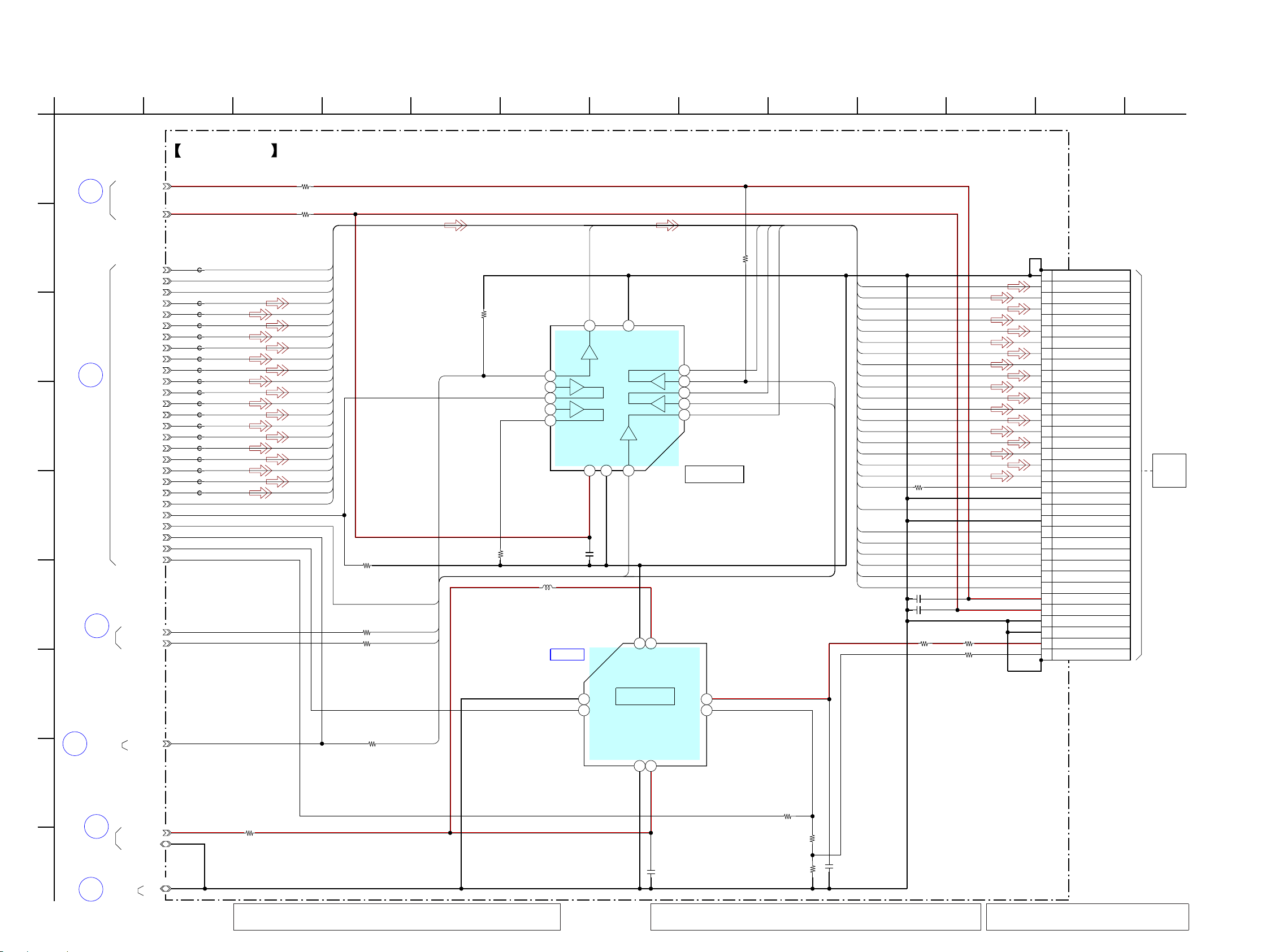
NWZ-S515/S516/S615F/S616F/S618F
NWZ-S515/S516/S615F/S616F/S618F
2626
5-10. SCHEMATIC DIAGRAM - MAIN Board (7/10) -
35
BOARD
(4/10)
MAIN
30
BOARD
(4/10)
MAIN
7
BOARD
(1/10)
MAIN
21
BOARD
(3/10)
MAIN
(5/10)
BOARD
37
MAIN
MAIN
36
BOARD
(2/10)
IC B/D
LCD_G5
LCD_B3
LCD_G4
LCD_B5
LCD_B2
LCD_R5
LCD_B4
LCD_HSYNC
LCD_R4
LCD_G2
LCD_R1
LCD_R3
LCD_R0
LCD_VSYNC
LCD_B0
LCD_G3
LCD_B1
LCD_G1
LCD_G0
LCD_PXCLK
LCD_R2
VDD_UNREG
LCD_PWM1
LCD_PON
LCD_PCI
VDD_LOG_F
VDD_ANA_F
SPI0_MOSI
SPI0_CLK
LCD_ENABLE
SPI0_XCS0
FB802
FB803
FB804
FB805
FB806
FB807
FB808
FB809
FB810
FB811
FB812
FB813
FB814
FB815
FB816
FB817
FB818
FB819
FB801
DGND
0R833
0
R832
33k
R830
470k
R828
0.1
C802
0.1
C803
0.1
C806
0.1
C805
SN74AUC34
IC802
5
2
3
4
87
GND
12
9
10
11
15
GND
114
VCC
6
13
BD6069GUT-E2
CSP
(Chip Size Package)
IC803
A1
GNDA
A2
EN
A3
TESTB1VIN
B3VFB
C1
VOUT
C2
SW
C3
GND
22uH
L801
1
C804
LCD_BLTCTL
35P
CN801
1
2
3
4
5
6
7
8
9
10
11
12
13
14
15
16
17
18
19
20
21
22
23
24
25
26
27
28
29
30
31
32
33
34
35
220k
R823
220k
R827
0
R826
18
R831
47k
R829
R824
0
0
R839
0
R840
R820
0
R821
0
R822
0
FB820
0
FB821
0
SPI0_XCS0
DGND
LCD_ENABLE
LCD_CLK
LCD_MOSI
LCD_XCS
LCD_XRESET
LCD_XRESET
B0
B1
B2
B3
B4
B5
G0
G1
G2
G3
G4
G5
R0
R1
R2
R3
R4
R5
LCD_ENABLE
PXCLK
LCD_HSYNC
LCD_VSYNC
LCD_XCS
LCD_CLK
LCD_MOSI
PXCLK
R5
R4
R3
R2
R1
R0
G5
G4
G3
G2
G1
G0
B5
B4
B3
B2
B1
B0
SPI0_MOSI_0
SPI0_CLK_0
SPI0_CLK_0
SPI0_LCD_XCS
SPI0_LCD_XCS
LCD_PON
SPI0_MOSI_0
LCD_PON
GND
GND
LED_-
SDI
B0
B1
B2
B3
B4
B5
G0
G1
G2
G3
G4
G5
R0
R1
R2
R3
R4
R5
RESET
VDDI (1.8V)
SCL
VDD (2.85V)
DOTCLK (5.6448MHz)
VSYNC
HSYNC
GND
LED_+
GND
GND
CS
ENABLE
MAIN BOARD
IC802
LEVEL SHIFT
IC803
LCD BACK
A
1012
H
B
1311
C
78
I
F
9643
G
D
5
E
12
(7/10)
LIGHT DRIVER
LCD801
LIQUID
CRYSTAL
DISPLAY
(Page 23)
(Page 23)
(Page 20)
(Page 21)
(Page 22)
(Page 24)
• See page 30 for IC Block Diagrams.
Note 3: When the LCD SUB ASSY (LCD801)
is replaced, refer to SUPPLEMENT-2.
Note 1: When the MAIN board is replaced, format it according to the “NOTE OF
MAIN BOARD REPLACING” (refer to page 4) of the servicing notes.
Note 2: When IC802 and IC803 on the MAIN board is damaged, exchange the
new MAIN board for the MAIN board which IC damaged.
Ver. 1.3
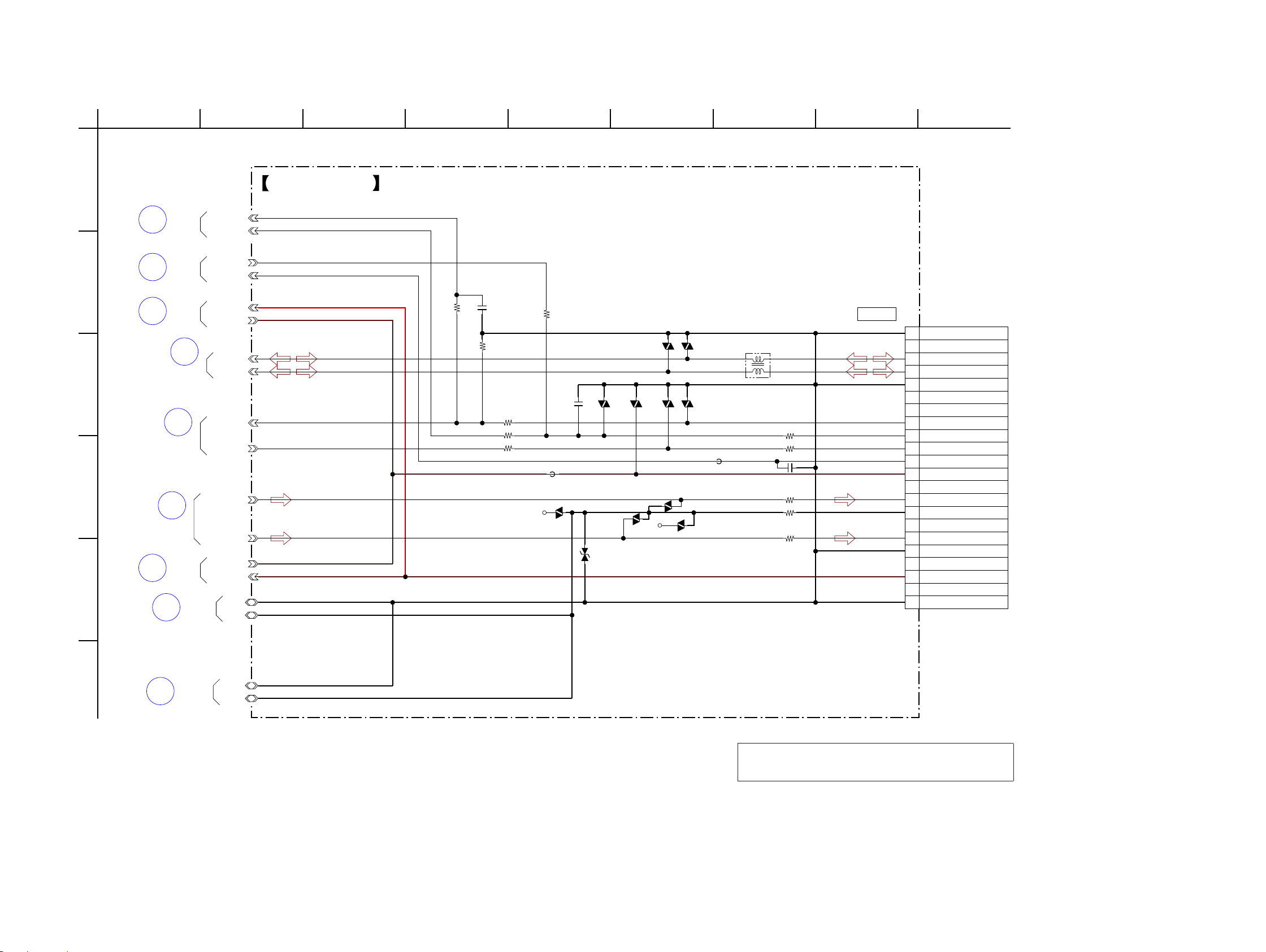
NWZ-S515/S516/S615F/S616F/S618F
NWZ-S515/S516/S615F/S616F/S618F
2727
5-11. SCHEMATIC DIAGRAM - MAIN Board (8/10) -
(4/10)
MAIN
34
BOARD
(4/10)
MAIN
27
BOARD
(1/10)
MAIN
13
BOARD
BOARD
40
MAIN
(10/10)
BOARD
MAIN
29
(4/10)
BOARD
MAIN
24
(4/10)
BOARD
23
MAIN
(3/10)
BOARD
41
MAIN
(10/10)
BOARD
MAIN
(10/10)
43
LF851
VCC_VBUS
USB_DM
USB_DP
UART_RXD
UART_TXD
LINE_OUT_R
LINE_OUT_L
CRD_AD
R855
47k
R851
1k
R853
1k
VDR851
VDR852
CN851
22P
1
2
3
4
5
6
7
8
9
10
11
12
13
14
15
16
17
18
19
20
21
22
DGND
CRD_DET
R857
470k
R858
10k
C853
100p
R859
1k
VDD_GP1_J
VCC_DCIN
VCC_VBAT
DGND
VDR853
VDR854
C854
0.01
FB854
0
FB855
0
FB857
0
FB851
0
FB852
0
VDR856
FB858
470p
C855
VDR858
VDR859
VDR860
VDR861
VDR862
RSB6.8STE61
D852
R861
AGND
VCC_VBAT
VCC_DCIN
AGND
AU_R_IN
RESERVE
UNREG_OUT
DCIN
D+
AU_R_OUT
RXD/WAKE
GND
TXD/SLEEP
DIGITAL_OUT/OPEN
CRD_AD
GND
USB_DET
GND
VIDEO-GND/GND
AU_L_IN
AU_COM
D-
AU_L_OUT
VIDEO-IN/OUT/OPEN
RESERVE(OTG)
VIN
(8/10)MAIN BOARDA
12
B
C
78
F
9643
D
5
E
WM-PORT
(Page 23)
(Page 29)
(Page 29)
(Page 22)
(Page 23)
(Page 20)
(Page 23)
(Page 23)
(Page 29)
Note: When the MAIN board is replaced, format it according to the
“NOTE OF MAIN BOARD REPLACING” (refer to page 4) of
the servicing notes.

NWZ-S515/S516/S615F/S616F/S618F
NWZ-S515/S516/S615F/S616F/S618F
2828
5-12. SCHEMATIC DIAGRAM - MAIN Board (9/10) -
36
MAIN
BOARD
(4/10)
10k
R885
15k
R887
10k
R882
C881
0.047
0.01
C882
0.01
C884
22k
R884
10k
R886
15k
R883
10k
R881
C883
0.047
CL890
CL891
CL888
KEY_AD0
KEY_AD1
AGND
KEY_WAKE0
8P
CN881
1GND
2LEFT
3
BACK/HOME
4UP
5PLAY/PAUSE
6 OPTION
7RIGHT
8DOWN
VOL+VOL-
(9/10)MAIN BOARDA
12
B
C
78643
D
5
SWITCH
SHEET
S888 S889
(Page 23)
Note 2: When CN881 on the MAIN board is damaged, exchange
the new MAIN board for the MAIN board which connector
damaged.
Note 1: When the MAIN board is replaced, format it according
to the “NOTE OF MAIN BOARD REPLACING” (refer to
page 4) of the servicing notes.
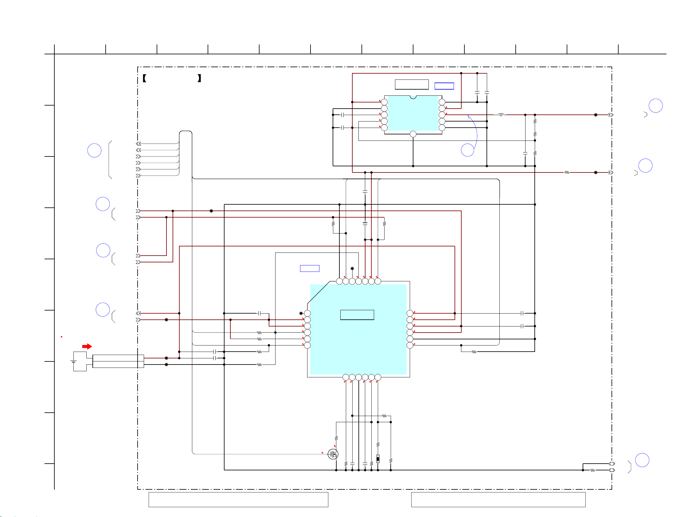
NWZ-S515/S516/S615F/S616F/S618F
NWZ-S515/S516/S615F/S616F/S618F
2929
5-13. SCHEMATIC DIAGRAM - MAIN Board (10/10) -
• See page 17 for Waveform. • See page 30 for IC Block Diagrams.
MAIN
(4/10)
33
BOARD
BOARD
19
(3/10)
MAIN
BOARD
43
(8/10)
MAIN
BOARD
41
(8/10)
MAIN
BOARD
3
(1/10)
MAIN
BOARD
22
(3/10)
MAIN
(8/10)
BOARD
40
MAIN
IC B/D
IC B/D
1
3.7
0
0
2.7
0
0
0
0
0
3.7
2.70
0
000
2.7
3.8
3.8
2.7
3.8
2.1
3.8
0.8
0.8
3.8
2.9
0
POWER ON: 45mA
TOTAL CURRENT
CL903
R911
470k
R906
3300
C905 0.068
IC901
MAX8677AETG
1
2
3
4
5
6
789101112
13 14 15 16 17 18
19202122232425
R909 22k
R907
470k
C909
22
C904
0.1
IC903
MAX1557ETB
IN
1
GND
2
SS
3
OUT
4
XSHDN
5
D2
6
PGND
7
LX
8
INP
9
D1
10
11
PGND
C911
0.001
R915
33k
C903
0.1
VDD_DDCOUT20
R914
47k
VCC_DCIN
VDD_GP1_J
XCHG_DET
CHG_XFLT
C912
22
DGND
C906
0.1
C907
22
CHG_XCHGEN
CHG_PEN2
USB_SUSPEND
C913
22
R903
470k
R904
470k
R901
0
AGND
R912
8200
VCC_VBAT
TH901
VCC_VBUS
C901
10
C920
4.7
R913
10k
VDD_UNREG
R902
0
CN901
1BATT+
2BATT-
Q903
2SK3541T2L
R919
10k
CHG_ICTL
R921
220k
R922
220k
C917
22
C921
22
C915
22
L901
4.7uH
R908
10k
CL901
CL902
1500
R905
33k
R910
CL911
CL912
CL913
CL914
CL915
VDD_GP1_J
VCC_VBUS
XCHG_DET
CHG_XFLT
CHG_XCHGEN
CHG_PEN2
USB_SUSPEND
CHG_ICTL
USB_SUSPEND
CHG_XFLT
CHG_XCHGEN
XCHG_DET
CHG_PEN2
CHG_ICTL
BAT
BAT
USB
USB
TSET
USUSS
/DONE
DC
DC
/CEN
PEN1
PEN2
GND
/FLT
/UOK
/DOK
SYS
/CHG
SYS
PSETVLGNDCTISET
THM
A
1012
H
B
11
C
78
I
F
9643
G
D
5
E
12
(10/10)MAIN BOARD
POWER CONTROL,
IC901
DC/DC CONVERTER
IC903
ION
LITHIUM
BATTERY
CHARGE CONTROL
CHARGE CONTROL SWITCH
S
3.7V 610mAh
(Page 23)
(Page 22)
(Page 27)
(Page 27)
(Page 20)
(Page 22)
(Page 27)
Note 2: When IC901 and IC903 on the MAIN board is damaged, exchange
the new MAIN board for the MAIN board which IC damaged.
Note 1: When the MAIN board is replaced, format it according to the “NOTE OF
MAIN BOARD REPLACING” (refer to page 4) of the servicing notes.
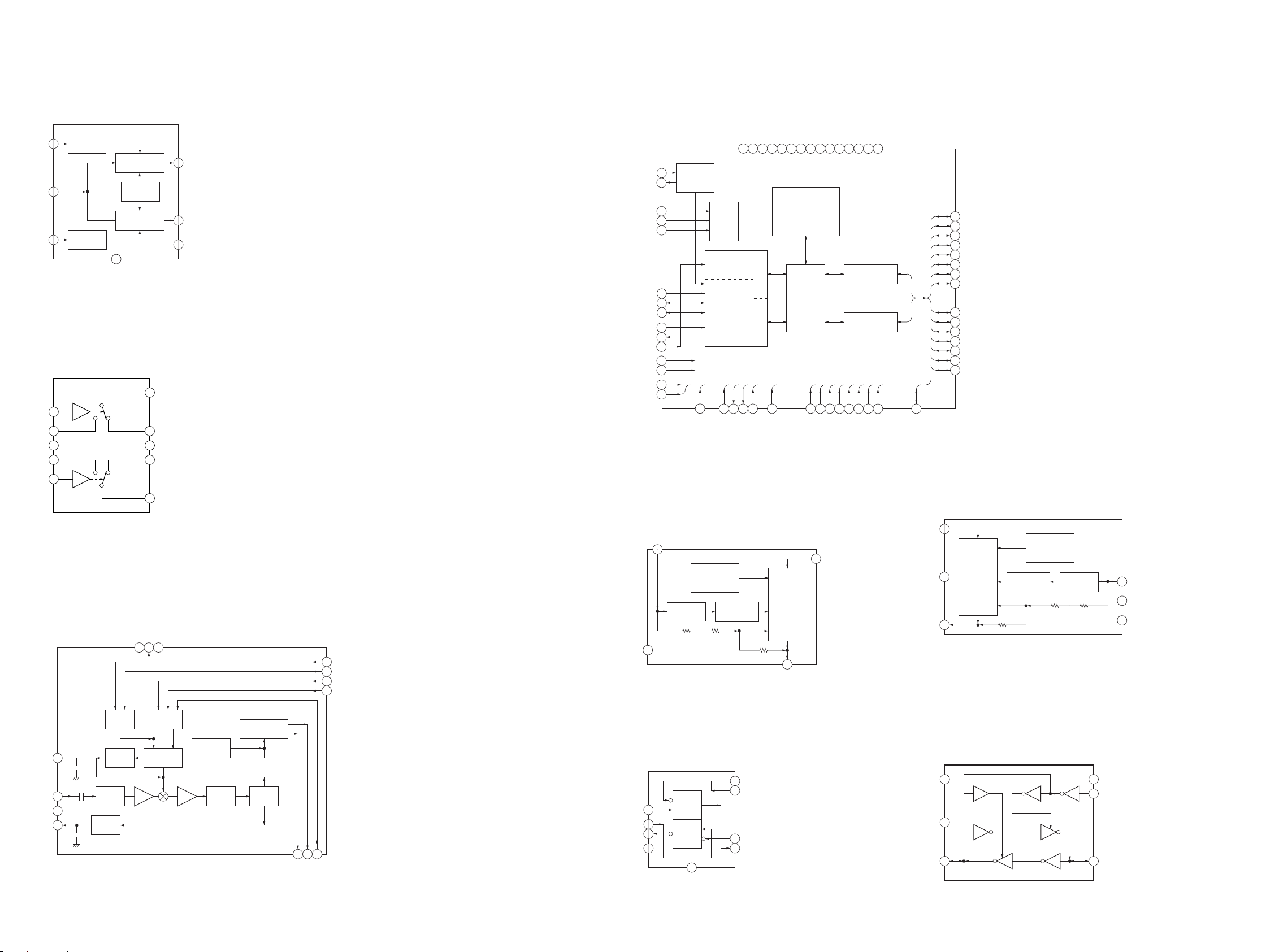
NWZ-S515/S516/S615F/S616F/S618F
NWZ-S515/S516/S615F/S616F/S618F
3030
• IC Block Diagrams
– MAIN Board –
IC301 XC6401FF58DR
IC303 MAX4745
IC403 SDFMM1N23GB2T
IC501 S1R72V17B00A20B
IC503, 602 TK63731BCB-G
IC504 TK63718HCL-G
IC505, 506 TC7WG74FC
IC509 SN74AVC1T45YZPR
B8
CHANNEL
OSCILLATOR
USB
NC
CPU INTERFACE
CONTROLLER
MULTI
TRANSCELVER
FIRST-IN FIRST-OUT
C8
F3
H2
E3
G4
F4
E1
C5
E2
D3
G1
F1
F2
H4
A1
C6
E8
D6
F8
E7
F7
G8
XWRH
CD0
CA8
CA7
CA6
CA5
CA4
CA3
CA2
XDACK
XDREQ
XINT
XCS
CD15
CD14
CD13
CD12
CD11
CD10
CD9
XI
XO
G3
XRD
TEST
MUX
H1
TESTEN
H8
ATPGEN
A8
BURNIN
MACRO
DEVICE SERIAL
INTERFACE
ENGINE
HOST SERIAL
INTERFACE
ENGINE
A6
R1
A3
DP
A4
DM
B1VBUSFLG
C1
VBUSEN
C3VBUS
D1
XRESET
D8
CLKIN
CONTROLLER
FIRST-IN FIRST-OUT
USB
DMA
CONTROLLER
H3
XWRL
VSS
G7
B7
B6
B5
B4
B2
CVDD
D7
LVDD
G2
LVDD
C7
LVDD
A7
LVDD
A2
HVDD
C2
HVDD
B3
HVDD
A5
H7
CD8
F6
G6
H6
E6
F5
H5
G5
CD7
CD6
CD5
CD4
CD3
CD2
CD1
C4
CA1
D2
XBEL
VSS
VSS
VSS
VSS
VSS
/ENDPOINT
OVER CURRENT
THERMAL &
PROTECTION
CONTROL
ON / OFF
REGULATOR
VOLTAGE
B2
VIN
VCONT
GND
A1
REFERENCE
A2
B1
VOUT
XQ
Q
C
D
R
S
9
GND
1
CK
2
D
3
XQ
4
GND
5
Q
6
XCLR
7
XPR
8
VCC
EN2
VIN
EN1
ON / OFF
1
CONTROL
2
ON / OFF
3
CONTROL
CB1
1
NO1
2
3
GND
NO2
4
REGULATOR 2
VOLTAGE
REFERENCE
REGULATOR 1
7
GND
6
VOUT2
5
VOUT1
4
VSS
10
COM1
NC1
9
8
VCC
NC2
7
CB2
5
GND13STO12D-GND
14
LOGIC
TUNING
SYSTEM
1VCC
2ANT
3GND
4RSSO
ANTENNA
RSSI
BUFFER
VCO
BALUN
CON26
IF
LAG-LEAD
FILTER
IF
FILTER
MPX DECODER
DEMODULATOR
LIMITER
5
AUDIO RIGHT
11 X2
10 X1
6
7
DA
AUDIO LEFT
9CL
8LA
1
VIN
THERMAL &
OVER CURRENT
PROTECTION
2
GND
VOUT
3
REGULATOR
VOLTAGE
REFERENCE
A1
VCCA
GND
B1
A
C1
ON / OFF
CONTROL
6
VCONT
5
GND
4
NC
A2
VCCB
B2
DIR
C2
B
 Loading...