Sony KDP-57XBR2, KDP-65XBR2 Service manual
SERVICE MANUAL
RA-5A
CHASSIS
MODEL
KDP-57XBR2 RM-Y185 US SCC-P69B-A
KDP-57XBR2 RM-Y185 Canadian SCC-P69B-A
KDP-65XBR2 RM-Y185 US SCC-P69A-A
KDP-65XBR2 RM-Y185 Canadian SCC-P69A-A
COMMANDER
DEST. CHASSIS NO.
RM-Y185
DIGITAL HIGH DEFINITION PROJECTION TV

KDP-57XBR2/65XBR2
SPECIFICATIONS
Projection System 3 picture tubes, 3 lenses, horizontal in-line system
Picture Tube 7-inch high-brightness monochrome tubes (6.3 raster size),
with optical coupling and liquid cooling system
Projection Lenses High performance, large diameter hybrid lens F1.05
Antenna 75 ohm external terminal for VHF/UHF
Television System NTSC, American TV Standard, ATSC
Channel Coverage
DTV 2-69
VHF 2-13
UHF 14-69
CATV 1-125
Power Requirements 120V AC, 60 Hz
Number of Inputs/Outputs
Video (IN) 4 total (1 on front panel) 1 Vp-p, 75 ohms unbalanced, sync negative
S Video (IN) 4 (1 on front panel) Y: 1 Vp-p, 75 ohms unbalanced, sync negative
Component Video Input 2 (Y, P
Audio (IN) 6 total (1 on front panel) 500 mVrms (100% modulation)
Audio (OUT) 1 More than 408 mVrms at the maximum volume setting (Variable)
Subwoofer (Out) 1 More than 408 mVrms at the maximum volume setting
SELECT OUT 1 Video 1 Vp-p, 75 ohms unbalanced, sync negative
Digital Audio Optical Output 1 Optical Rectangular (1)
Dolby Digital/PCM
CONTROL S (IN/OUT) 1
i.LINK S200 2 4-pin S200 i.LINK terminal (2)
Supplied Accessories
Remote Control RM-Y185
AA (R6) Batteries 2 supplied for remote control
Optional Accessories
AV Cable VMC-810/820/830 HG
Audio Cable RKC-515HG
i.LINK Cable VMC-IL4415 (4-pin to 4-pin, 1.5 meters), VMC-IL4435 (4-pin to 4-pin, 3.5 meters)
Component Video Cable VMC-10/30 HG
Rear Speakers SS-MB115
Screen Size 57 in measured diagonally (KDP-57XBR2)
Speakers Tweeter 100 mm (4") × 2
Speaker Output Front 20 W × 2
Dimensions (W × H × D) 1380 × 1400 × 680 mm (54 3/8 × 55 1/8 × 26 7/8 in) (KDP-57XBR2)
Mass 126 kg (277 lbs) (KDP-57XBR2)
Power Consumption
In Use 280 W
In Standby 0.9 W
In i.LINK Standby 24 W
Design and specifications are subject to change without notice.
, PR) Y: 1.0 Vp-p, 75 ohms unbalanced, sync negative
B
1 Audio More than 408 mVrms (100% modulation)
65 in measured diagonally (KDP-65XBR2)
Woofer 160 mm (6 3/8") × 2
Center 100 mm (4") × 2
Center 20 W × 1
Rear 20 W × 2
1558 × 1574 × 735 mm (61 3/8 × 62 × 29) (KDP-65XBR2)
148 kg (326 lbs) (KDP-65XBR2)
C: 0.286 Vp-p, (Burst signal), 75 ohms
PB: 0.7 Vp-p, 75 ohms
PR: 0.7 Vp-p, 75 ohms
Impedance: 47 kilohm
More than 408 mVrms (Fixed)
Impedance (output): 2 kilohms
Impedance (output): 2 kilohms
Cutoff frequency: 100 Hz
Impedance (output): 2 kilohms
RM-Y185
– 2 –
SAFETY CHECK-OUT
(US Model only)
KDP-57XBR2/65XBR2
RM-Y185
After correcting the original service problem, perform the following safety checks before releasing the set to the customer:
1. Check the area of your repair for unsoldered or poorly-soldered connections. Check the entire board surface for solder
splashes and bridges.
2. Check the interboard wiring to ensure that no wires are
“pinched” or contact high-wattage resistors.
3. Check that all control knobs, shields, covers, ground straps,
and mounting hardware have been replaced. Be absolutely
certain that you have replaced all the insulators.
4. Look for unauthorized replacement parts, particularly transistors, that were installed during a previous repair. Point them
out to the customer and recommend their replacement.
5. Look for parts which, though functioning, show obvious signs
of deterioration. Point them out to the customer and recommend their replacement.
6. Check the line cords for cracks and abrasion. Recommend the
replacement of any such line cord to the customer.
7. Check the condition of the monopole antenna (if any).
Make sure the end is not broken off, and has the plastic cap on
it. Point out the danger of impalement on a broken antenna to
the customer, and recommend the antenna’s replacement.
8. Check the B+ and HV to see if they are specified values. Make
sure your instruments are accurate; be suspicious of your HV
meter if sets always have low HV.
9. Check the antenna terminals, metal trim, “metallized” knobs,
screws, and all other exposed metal parts for AC Leakage.
Check leakage as described below.
To Exposed Metal
Parts on Set
LEAKAGE TEST
The AC leakage from any exposed metal part to earth ground
and from all exposed metal parts to any exposed metal part having a
return to chassis, must not exceed 0.5 mA (500 microamperes).
Leakage current can be measured by any one of three methods.
1. A commercial leakage tester, such as the Simpson 229 or
RCA WT-540A. Follow the manufacturers’ instructions to
use these instruments.
2. A battery-operated AC milliammeter. The Data Precision 245
digital multimeter is suitable for this job.
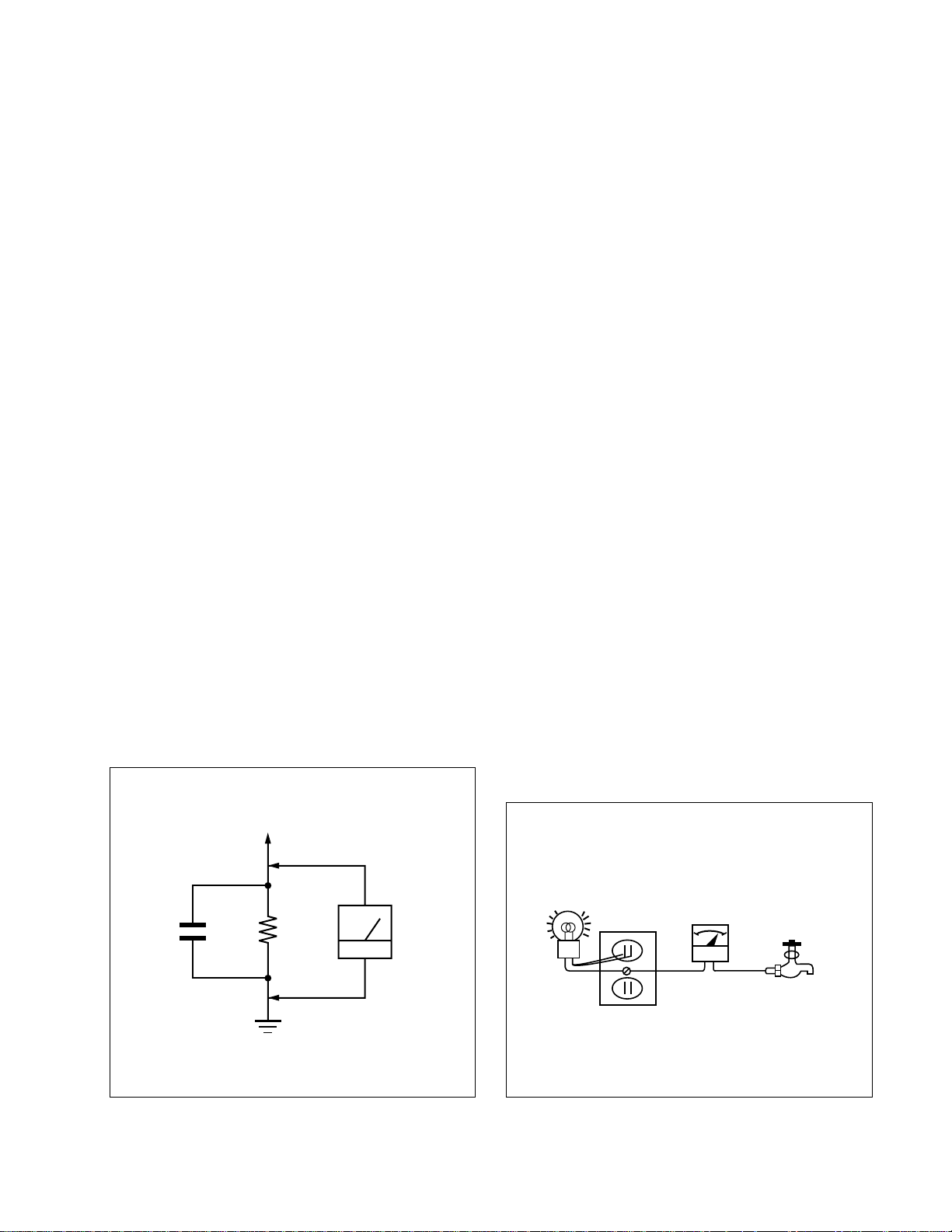
3. Measuring the voltage drop across a resistor by means of a
VOM or battery-operated AC voltmeter. The “limit” indica-
tion is 0.75 V, so analog meters must have an accurate low-
voltage scale. The Simpson 250 and Sanwa SH-63Trd are ex-
amples of a passive VOMs that are suitable. Nearly all battery
operated digital multimeters that have a 2 V AC range are suit-
able. (See Fig. A)
HOW TO FIND A GOOD EARTH GROUND
A cold-water pipe is guaranteed earth ground; the cover-plate
retaining screw on most AC outlet boxes is also at earth ground. If
the retaining screw is to be used as your earth-ground, verify that it
is at ground by measuring the resistance between it and a coldwater pipe with an ohmmeter. The reading should be zero ohms. If
a cold-water pipe is not accessible, connect a 60 – 100 watts
trouble light (not a neon lamp) between the hot side of the receptacle and the retaining screw. Try both slots, if necessary, to locate
the hot side of the line, the lamp should light at normal brilliance if
the screw is at ground potential. (See Fig. B)
0.15 µF
1.5 k
Ω
Earth Ground
AC
Voltmeter
(0.75 V)
Fig. A. Using an AC voltmeter to check AC leakage.
– 3 –
Trouble Light
AC Outlet Box
Ohmmeter
Fig. B. Checking for earth ground.
Cold-water Pipe

TABLE OF CONTENTS
Section Title PageSection Title Page
KDP-57XBR2/65XBR2
RM-Y185
1. SELF DIAGNOSIS FUNCTION ...................... 6
2. DISASSEMBLY
2-1. Rear Board Removal ......................................... 9
2-2. Main Bracket Block Removal ........................... 9
2-3. Service Position ................................................. 9
2-4. Terminal board Removal .................................. 9
2-5. G Board Removal ............................................... 10
2-6. D Board Removal ............................................... 10
2-7. AD, U, B and A Boards Removal...................... 11
2-8. Q-box Assembly Removal ................................. 11
2-9. K Board Removal ............................................... 12
2-10. Resistor Assembly (Focus Pack) Removal ........ 12
2-11. Screen Frame Block Assembly .......................... 13
2-12. S Board Removal................................................ 13
2-13. Control Panel Block Removal ........................... 14
2-14. HD Board Removal ............................................ 14
2-15. Control Door Block Assembly ........................... 15
2-16. HB Board Removal ............................................ 15
2-17. HA Board Removal ............................................ 16
2-18. Picture Tube Block Removal ............................. 16
2-19. High-Voltage Cable Removal and Installation ... 17
2-20. Picture Tube Removal ........................................ 17
3. SET-UP ADJUSTMENTS
3-1. Screen Voltage Adjustment
(Rough Alignment) ........................................... 18
3-2. Screen (G2) Adjustment .................................... 18
3-3. Deflection Yoke Tilt Adjustment ...................... 18
3-4. Focus Lens Adjustment...................................... 19
3-5. Focus VR Adjustment ....................................... 19
3-6. 2-Pole Magnet Adjustment ................................ 19
3-7. Centering Magnet Adjustment .......................... 20
3-8. 4-Pole Magnet Adjustment ................................ 20
3-9. Defocus Adjustment (Blue) ............................... 20
3-10. Electrical Adjustment
by Remote Commander...................................... 21
3-11. Registration Adjustment ................................... 40
3-11-1. Setup for Adjustment .................................... 40
3-11-2 Main Deflection Adjustment ........................ 40
3-11-3. Operation Method
for Projectoe Engine Mode ............................ 41
3-11-4. Projector Engine Adjustment
(Sub Deflection Adjustment)......................... 42
3-12. Auto Registration Offset .................................... 44
3-13. Auto Registration Error Code List ..................... 45
4. CIRCUIT ADJUSTMENTS
4-1. 480p Y, PB, PR Gain Adjustment ..................... 46
4-2. Main Y/C Level Adjustment
(for the DRC Path) ............................................. 46
4-3. Main Y/C Level Adjustment
(for the VDO Path) ............................................. 46
4-4. SUB Y/C Level Adjustment
(for the DRC Path) ............................................. 47
4-5. SUB Y/C Level Adjustment
(for the VDO Path) ............................................. 47
4-6. Main Decoder Sub Contrast Adjustment
(for Composite and Y/C Inputs) ........................ 47
4-7. Main Decoder Sub Color and Sub Hue
Adjustment (for Composite and Y/C Inputs) .... 47
4-8. Sub Decoder Sub Contrast Adjustment
(for Y/C Input).................................................... 48
4-9. Sub Decoder Sub Color and Sub Hue
Adjustment (for Y/C Input)................................ 48
4-10. Sub Decoder Sub Contrast Adjustment
(for Composite Input)......................................... 48
4-11. Sub Decoder Sub Color and Sub Hue
Adjustment (for Composite Input)..................... 48
4-12. Main Decoder PB and PR Offset Adjustment ... 49
4-13. Sub Decoder PB and PR Offset Adjustment ..... 49
4-14. Blue Offset Adjustment...................................... 49
4-15. Sub Contrast Adjustment ................................... 49
4-16. Sub Color and Sub Hue Adjustment .................. 50
4-17. RF Sub Contrast Adjustment ............................. 50
4-18. RF Sub Color and Sub Hue Adjustment ............ 50
5. SAFETY RELATED ADJUSTMENTS
5-1. HV Regulation Circuit Check and
Adjustment ......................................................... 51
5-2. HV Hold Down Circuit Operation Check and
Adjustment ......................................................... 51
5-3. +B Max Voltage Confirmation .......................... 51
5-4. +B OVP Confirmation ....................................... 51
6. FIRMWARE UPGRADES
6-1. Overview ............................................................ 52
6-2. Transferring the New Firmware
from the Memory Stick to the Q-Box ................ 52
7. DIAGRAMS
7-1. Block Diagram (1).............................................. 53
Block Diagram (2).............................................. 54
Block Diagram (3).............................................. 55
Block Diagram (4).............................................. 56
Block Diagram (5).............................................. 57
Block Diagram (6).............................................. 58
Block Diagram (7).............................................. 59
– 4 –

KDP-57XBR2/65XBR2
RM-Y185
Section Title PageSection Title Page
Block Diagram (8).............................................. 60
Block Diagram (9).............................................. 61
Block Diagram (10)............................................ 62
7-2. Frame Schematic Diagram................................. 63
7-3. Circuit Boards Location ..................................... 64
7-4. Schematic Diagrams and Printed Wiring
Boards ................................................................. 64
(1) Schematic Diagram of A (1/3) Board................ 65
(2) Schematic Diagram of A (2/3) Board ............... 66
(3) Schematic Diagram of A (3/3) Board ............... 67
(4) Schematic Diagram of AD (1/2) Board ............ 68
(5) Schematic Diagram of AD (2/2) Board............. 69
(6) Schematic Diagram of B (1/7) Board ................ 70
(7) Schematic Diagram of B (2/7) Board ................ 71
(8) Schematic Diagram of B (3/7) Board ................ 72
(9) Schematic Diagram of B (4/7) Board ................ 73
(10) Schematic Diagram of B (5/7) Board ................ 74
(11) Schematic Diagram of B (6/7) Board ................ 75
(12) Schematic Diagram of B (7/7) Board ................ 76
(13) Schematic Diagrams of CB and CG Boards...... 77
(14) Schematic Diagrams of CR and V Boards ........ 78
(15) Schematic Diagram of D (1/3) Board ................ 79
(16) Schematic Diagram of D (2/3) Board ................ 80
(17) Schematic Diagram of D (3/3) Board ................ 81
(18) Schematic Diagram of G (1/2) Board ................ 82
(19) Schematic Diagram of G (2/2) Board ................ 83
(20) Schematic Diagrams of HA, HB, HC and
HD Boards .......................................................... 84
(21) Schematic Diagram of K (1/3) Board ................ 85
(22) Schematic Diagram of K (2/3) Board ................ 86
(23) Schematic Diagram of K (3/3) Board ................ 87
(24) Schematic Diagrams of S and U Boards............ 88
Printed Wiring Boards
• A Board ............................................................ 89
• AD Board ......................................................... 91
• B Board ............................................................ 92
• CB and CG Boards .......................................... 94
• CR and V Boards ............................................. 95
• D Board ............................................................ 96
• G Board ............................................................ 97
• HA, HB, HC and HD Boards .......................... 99
• K Board ............................................................ 100
• U and S Boards ................................................ 102
7-5. Waveforms ........................................................ 103
7-6. IC Block Diagrams ............................................ 105
7-7. Semiconductors ................................................. 108
8. EXPLODED VIEWS
8-1. Screen and Screen Frame Block ...................... 109
8-2. Cabinet Block .................................................... 110
8-3. Control Panel Block ........................................... 111
8-4. Main Bracket Block ........................................... 112
8-5. Picture Tube Block............................................. 113
9. ELECTRICAL PARTS LIST ............................ 114
WARNING!!
NEVER TURN ON THE POWER IN A CONDITION IN
WHICH THE DEGAUSS COIL HAS BEEN REMOVED.
SAFETY-RELATED COMPONENT WARNING!!
COMPONENTS IDENTIFIED BY SHADING AND MARK
¡ ON THE SCHEMATIC DIAGRAMS, EXPLODED
VIEWS AND IN THE PARTS LIST ARE CRITICAL FOR
SAFE OPERATION. REPLACE THESE COMPONENTS
WITH SONY PARTS WHOSE PART NUMBERS APPEAR AS SHOWN IN THIS MANUAL OR IN SUPPLEMENTS PUBLISHED BY SONY. CIRCUIT ADJUSTMENTS THAT ARE CRITICAL FOR SAFE OPERATION
ARE IDENTIFIED IN THIS MANUAL. FOLLOW THESE
PROCEDURES WHENEVER CRITICAL COMPONENTS
ARE REPLACED OR IMPROPER OPERATION IS SUSPECTED.
AVERTISSEMENT!!
NE JAMAIS METTRE SOUS TENSION QUAND LA
BOBINE DE DEMAGNETISATION EST ENLEVÉE.
ATTENTION AUX COMPOSANTS RELATIFS À LA
SÉCURITÉ!!
LES COMPOSANTS IDENTIFIÉS PAR UNE TRAME ET
UNE MARQUE
NE LES REMPLACER QUE PAR UNE PIÈCE PORTANT LE
NUMÉRO SPECIFIÉ. LES RÉGLAGES DE CIRCUIT DONT
L’IMPORTANCE EST CRITIQUE POUR LA SÉCURITÉ DU
FONCTIONNEMENT SONT IDENTIFIÉS DANS LE
PRÉSENT MANUEL. SUIVRE CES PROCÉDURES LORS
DE CHAQUE REMPLACEMENT DE COMPOSANTS CRITIQUES, OU LORSQU’UN MAUVAIS FONCTIONNEMENT
EST SUSPECTÉ.
¡ SONT CRITIQUES POUR LA SÉCURITÉ.
– 5 –
KDP-57XBR2/65XBR2
Note1: If a +B overcurrent is detected, stoppage of the vertical deflection is detected simultaneously. The sympton that is diagnosed first by the microcontroller is displayed on screen.
Note 2: Refer to Screen (G2) Adjustment in Section 3-1, 2 of this manual.
Note 3: If STANDBY/i. LINK STANDBY indicator blinks six (6) times, unplug the unit and wait 10 minutes before performing the adjustment.
Deteced symptoms
Diagnosis Item
No. of times
STANDBY / i. STANDBY
indicator blinks
Probable Cause Location
7 timesHorizontal deflection stopped • Q8035, 8038 is shorted. (D board)
0Power does not turn on
• Power cord is not plugged in.
• Fuse is burned out (F6001) (G board)
• Power does not come on.
• No power is supplied to the unit.
• AC power supply is faulty.
2 times
+B overcurrent (OCP)
(See Note 1)
• H. OUT (Q8024) is shorted. (D board)
• +B PWM (Q8035, 8038) is shorted. (D board)
• Power does not come on.
• Load on power line is shorted.
3 times+B overvoltage (OVP)
• IC6104 is faulty (G board)
• PH6002 is faulty (G board)
• Has entered standby mode.
4 timesVertical deflection stopped
• ±15 V is not supplied. (D board)
• IC8003 is faulty. (D board)
• Has entered standby state after horizontal raster.
• Vertical deflection pulse is stopped.
• Power line is shorted or power supply is stopped.
5 times
White balance failure
(Not balanced)
• Video out (IC3701, 3801, 3901) is faulty. (CR, CG, CB board)
• CRT drive (IC3006) is faulty. (A board)
• G2 is improperly adjusted. (See Note 2)
• No raster is generated.
• CRT cathode current detection reference pulse output is small.
6 times
LOW +B OCP/OVP
(Overcurrent/over voltage)
(See Note 3)
• LOW +B line is overloaded. (A, B boards)
• LOW +B line is shorted. (A, B boards)
• No picture
SECTION 1
SELF DIAGNOSIS FUNCTION
1. Summary of Self-Diagnosis Function
• This device includes a self-diagnosis function.
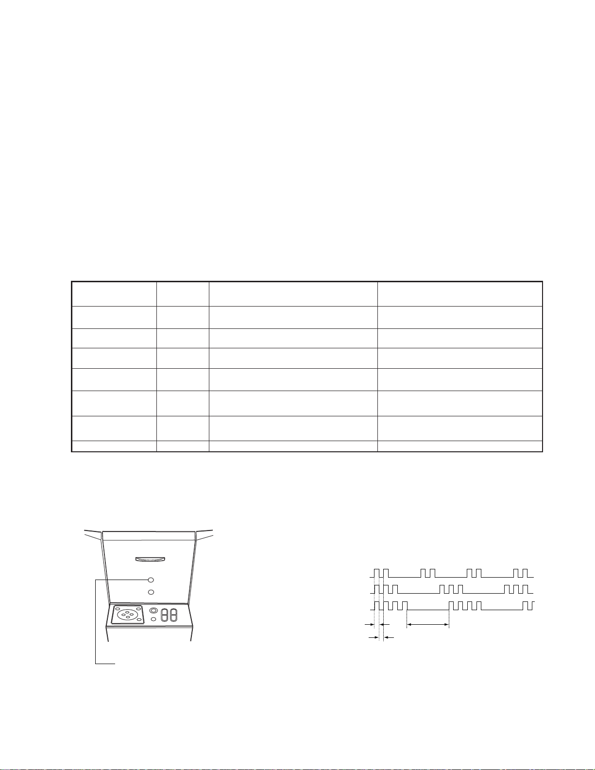
• In case of abnormalities, the STANDBY/i. LINK STANDBY indicator automatically blinks. It is possible to predict the abnormality
location by the number of blinks. The Instruction Manual describes blinking of the STANDBY/i. LINK STANDBY indicator.
• If the symptom is not reproduced sometimes in case of a malfunction, there is recording of whether a malfunction was generated or
not. Operate the remote command to confirm the matter on the screen and to predict the location of the abnormality.
2. Diagnosis Items and Prediction of Malfunction Location
• When a malfunction occurs the STANDBY/i. LINK STANDBY indicator only blinks for one of the following diagnosis items. In
case of two or more malfunctions, the item which first occurred blinks. If the malfunctions occurred simultaneously, the item with
the lower blink count blinks first.
• The screen display displays the results regarding all the diagnosis items listed below. The display “ 0 ” means that no malfunctions
occurred.
RM-Y185
3. Blinking count display of STANDBY / i. LINK STANDBY indicator
* One blink is not used for self-diagnosis.
< FRONT PANEL >
•EXAMPLE
POWER
STAND BY/
Release of STANDBY/i. LINK STANDBY indicator blinking.
• The STANDBY/i. LINK STANDBY indicator blinking display is released by turning OFF
the power switch on the TV main unit or removing the plug from the power.
i.LINK STAND BY
TIMER
STANDBY/i. LINK STANDBY indicator
<Diagnosis Items> <Number of Blinks>
• +B overcurrent 2 times
• +B overvoltage 3 times
• Vertical deflection stop 4 times
Lamp ON : 0.3 seconds
Lamp OFF : 0.3 seconds
– 6 –
Lamp OFF :
3.0 seconds

KDP-57XBR2/65XBR2
4. Self-diagnosis screen displays
• In cases of malfunctions where it is not possible to determine the symptom such as when the power goes off occasionally or when the
screen disappears occasionally, there is a screen display on whether the malfunction occurred or not in the past (and whether the
detection circuit operated or not) in order to allow confirmation.
<Screen Display Method>
• Quickly press the remote command button in the following order from the standby state.
DISPLAY b Channel 5 b VOL – b POWER
J
Be aware that this differs from the method of
entering the service mode (volume + ).
Self-Diagnosis screen display
Self Diagnosis
RM-Y185
2:+B OCP 0
Numeral “0” means that no fault has been detected.
3:+B OVP 0
4:V STOP 0
5:AKB 1
Numeral “1” means a fault was detected one time only.
6:Low B 0
7:H STOP 0
101:WDT 0
Serial: xxxxxxx
Model:xxxxxxxx
5. Self-Diagnosis Screen Display
• The results display is not automatically cleared. In case of repairs and after repairs, check the self-diagnosis screen and be sure to
return the results display to “ 0 ”.
• If the results display is not returned to “ 0 ” it will not be possible to judge a new malfunction after completing repairs.
<Method of Clearing Results Display>
1. Power off (Set to the standby mode)
2. DISPLAY b Channel 5 b VOL + b POWER (Service Mode)
3. Channel 8 b ENTER (Test reset = Factory preset condition)
<Method of Ending Self Diagnosis Screen>
• When ending the self-diagnosis screen completely, turn the power switch OFF on the remote commander or the main unit.
– 7 –
KDP-57XBR2/65XBR2
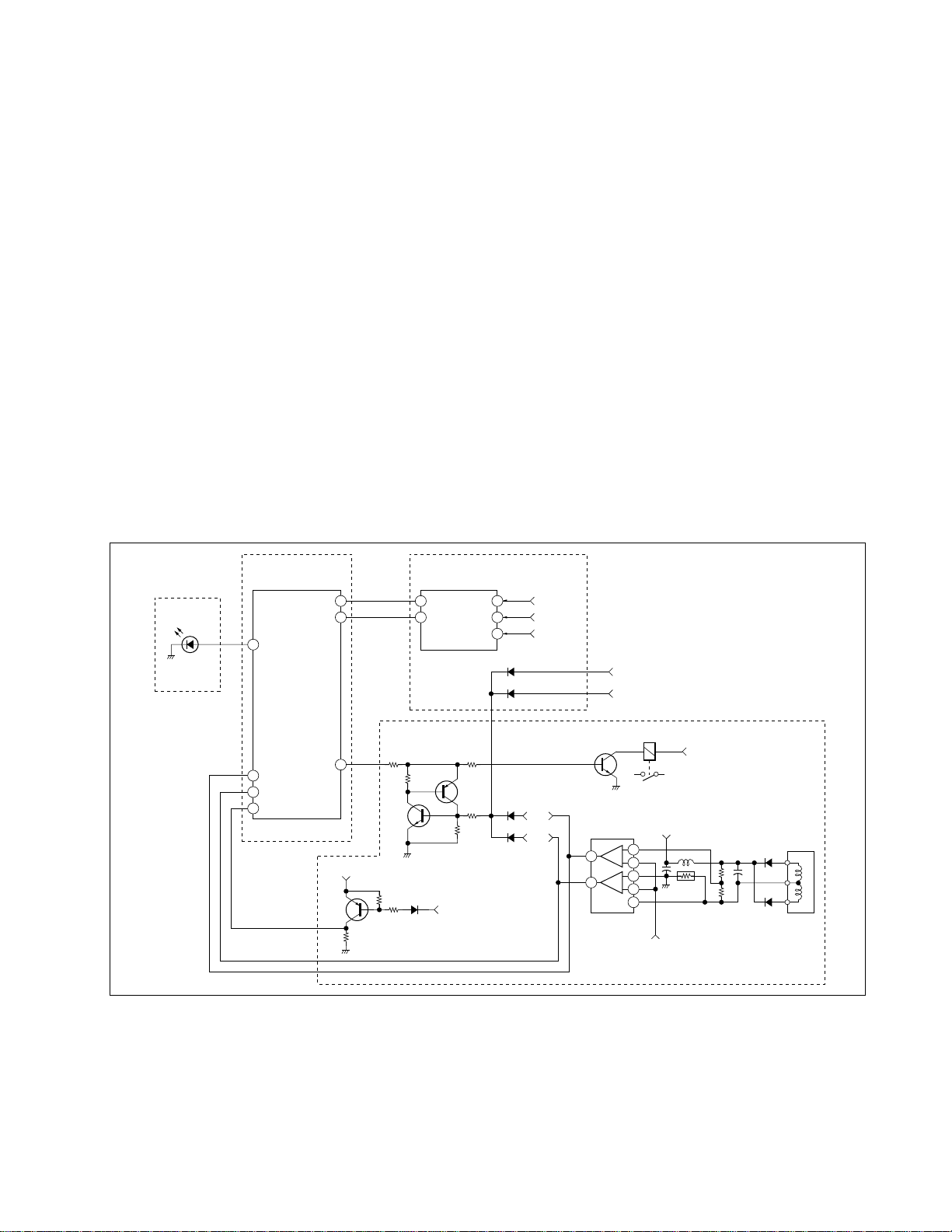
6. Self-diagnosis function operation
OCP Low B and +B line detect DET SHORT, and shut-down POWER ON RELAY.
Reset by turning power on/off.
In case of +B is loaded approx. 1.5 A or more, microcomputer detects it via IC6102.
OVP In case of +B becomes approx. 150 V or more, POWER ON RELAY shuts down and microcomputer detects it
via IC6102.
Reset by turning power on/off just the same as OCP.
Low B Occurs when set +6.5 V (D) is out.
V Stop In case of V DRIVE is disappeared, IC3006 detects it and shut-down POWER ON RELAY. Microcomputer
detects it and makes LED blinking.
AKB IK detection. Makes LED blinking in case of microcomputer doesn't detect IK returns of IC3006 (CXA2150AQ)
20 seconds or more.
H Stop In case of H DRIVE is disappeared, IC3006 detects it and shut-down POWER ON RELAY. Microcomputer
receives H Stop data from IC3006 and makes LED blinking.
RM-Y185
Self-diagnosis block diagram
IC001
MAIN CPU
D1350
STBY LED
48 STR/
STBY LED
HD board
45 OVP
44 OCP
43 LOW B ERR
B board
CLKO 29
DATO
AC RLY
30
69
STBY 5V
Q6121
IC3006
Y/C JUNGLE
26 SCL
25 SDA
A board
Q6105
Q6119
+6.5V (D)
AKB 58
VPROT 35
HPROT 34
D3003
D3013
D6123
D6124
OVP
OCP
IK
VP
HP
HV PROT
AUDIO PROT
RY6001
Q6120
IC6102
OVP/OCP DET
+
5
7
–
6
+
3
1
–
2
4
COM
From D board
+B
+
V REF
From K board
SET ON
T6001
+
– 8 –
G board
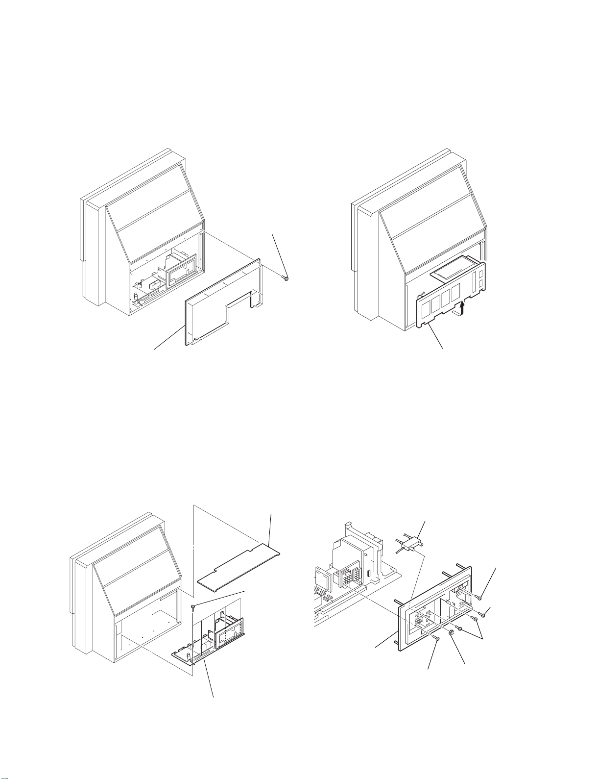
SECTION 2
1 Three screws
(+BVTP 3 x 12)
3 Two washers
4 Anntenna switch
5 Terminal board
1 Five screws
(+BVTP 3 x 12)
1 Six screws
(+BVTP 3 x 12)
2 Screw
(+BVTP 4 x 12)
DISASSEMBLY
KDP-57XBR2/65XBR2
RM-Y185
2-1. REAR BOARD REMOVAL
2 Rear board
2-3. SERVICE POSITION
1 Fourteen
(HEX tap)
Main bracket block
2-2. MAIN BRACKET BLOCK REMOVAL
1 Shield board
2 Five screws
3 Main bracket block
(HEX tap)
2-4. TERMINAL BOARD REMOVAL
– 9 –
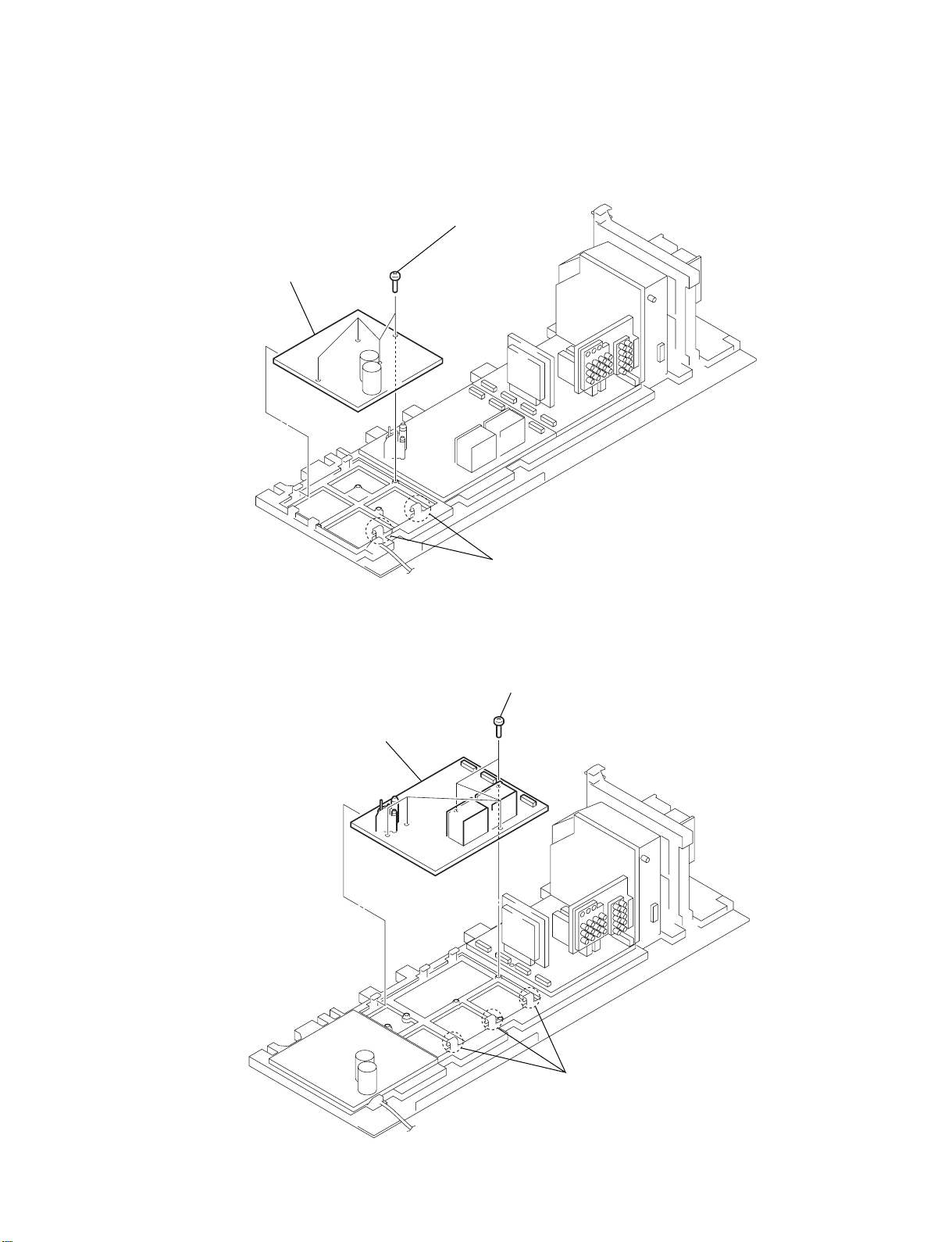
2-5. G BOARD REMOVAL
3 G board
KDP-57XBR2/65XBR2
RM-Y185
1 Four screws
(+BVTP 3X12)
2-6. D BOARD REMOVAL
2 Two claws
1 Five screws
(+BVTP 3X12)
3 D board
– 10 –
2 Three claws
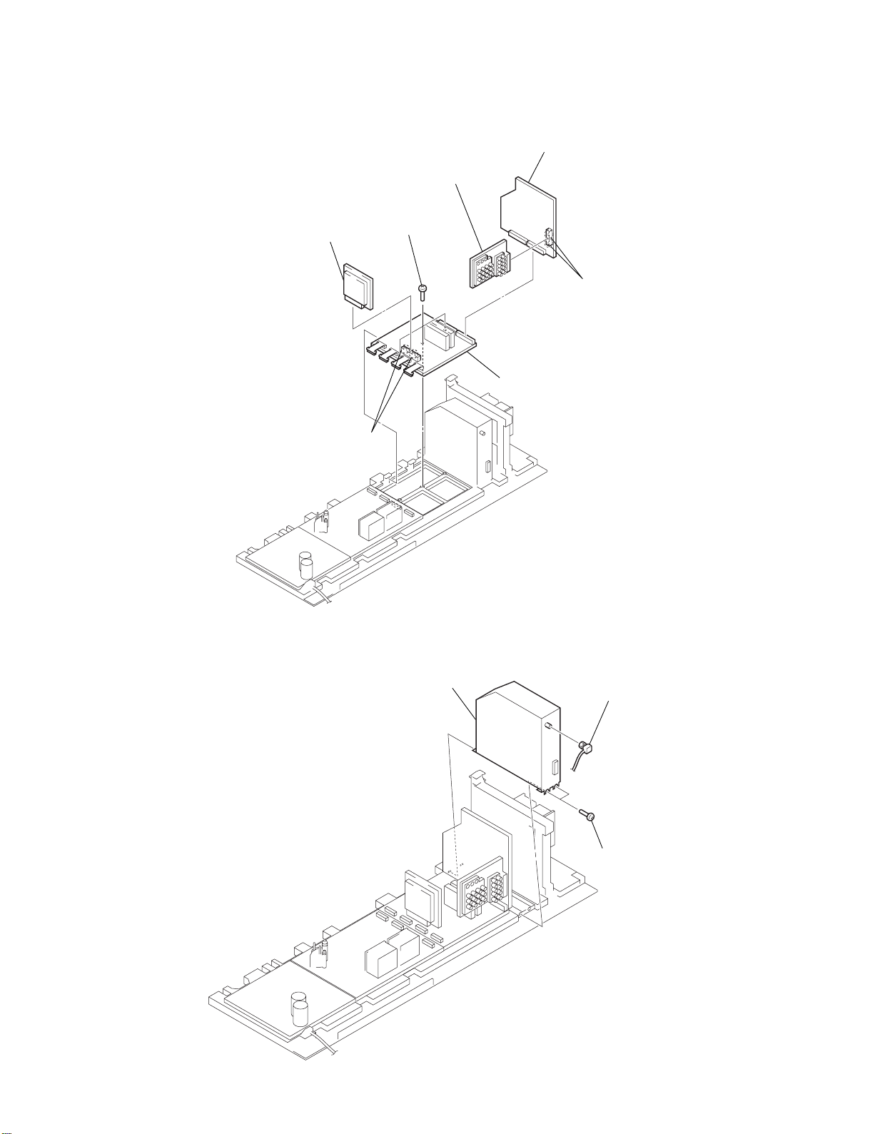
2-7. AD, U, B, AND A BOARDS REMOVAL
4 U board
6 Three screws
2 AD board
1 Two claws
(+BVTP 3X12)
KDP-57XBR2/65XBR2
RM-Y185
5 B board
3 Two claws
7 A board
2-8. Q-BOX ASSEMBLY REMOVAL
3 Q-box assembly
1 Cord with connector
(F-type)
2 Two screws
(+BVTP 4X12)
– 11 –
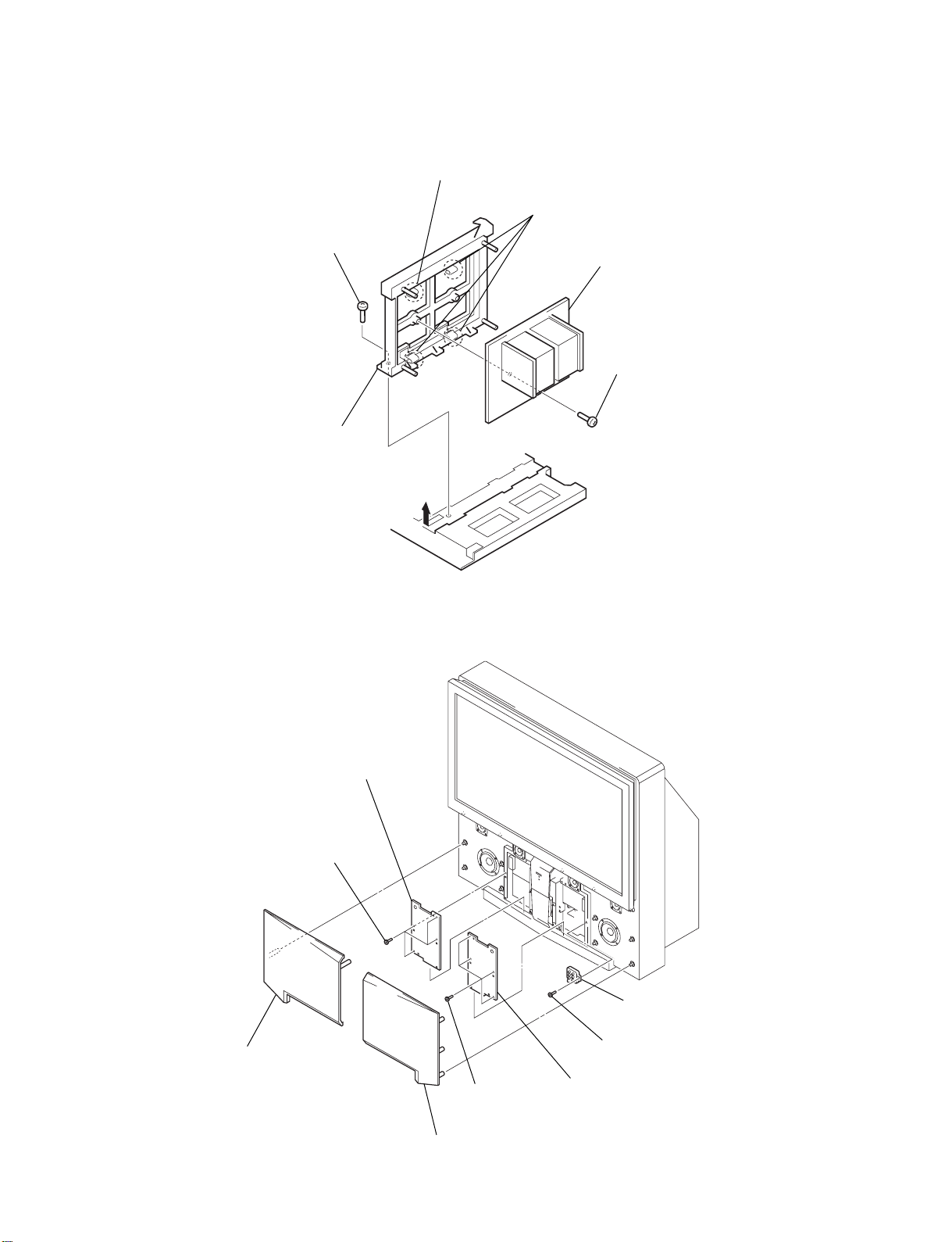
2-9. K BOARD REMOVAL
1 Screw
(+BVTP 4X12)
5 K board
bracket
KDP-57XBR2/65XBR2
RM-Y185
4 Claw
4 Tree claws
6 K board
3 Screw
(+BVTP 3X12)
2
2-10. RESISTOR ASSEMBLY (FOCUS PACK) REMOVAL
6 Front board (65)
5 Four screws
(HEX tap)
2 Speaker grille (L)
assembly
3 Four screws
(HEX tap)
1 Speaker grille (R)
assembly
– 12 –
8 Resistor assembly
(forcus pack)
7 Screw
(+BVTP 3X12)
4 Front board (65)
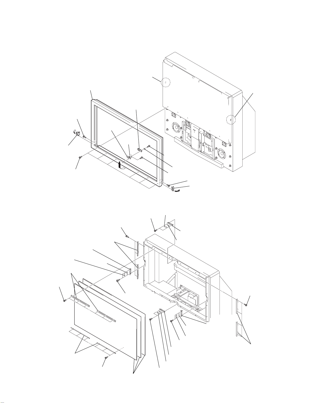
2-11. SCREEN FRAME BLOCK ASSEMBLY
7 Six screws
(HEX tap)
9 Screen block
1 Four screws
(HEX tap)
0 Two screws
(HEX tap)
0 Two screws
(HEX tap)
qs Sensor bracket (B)
qs Sensor bracket (B)
qa AR sensor bracket
qa AR sensor bracket
qd S board
qs Sensor bracket (B)
qa AR sensor bracket
qd S board
qd S board
qd S board
0 Two screws (HEX tap)
0 Two screws
(HEX tap)
qs Sensor bracket (B)
qa AR sensor
bracket
3 Four screws
(HEX tap)
2 Two screen holders (S)
4 Two screen
holders (S)
8 Two screen
holders (L)
6 Two screen
holders (L)
5 Six screws
(HEX tap)
8 Claw
9 Screen frame block
assembly
qg HC board
6 Screw (HEX tap)
KDP-57XBR2/65XBR2
RM-Y185
8 Claw
4
5 Screw cover
7 Six screws (HEX tap)
2-12. S BOARD REMOVAL
qf HC bracket
qd Claw
qa Screw
(+BVTP 4 x 12)
qs Harness
q; Screw (+BVTP 4 x 12)
3 Screw (HEX tap)
2 Screw cover
1
– 13 –
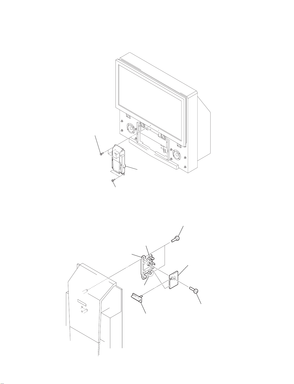
2-13. CONTROL PANEL BLOCK ASSEMBLY
1 Four screws
(HEX tap)
KDP-57XBR2/65XBR2
RM-Y185
2-14. HD BOARD REMOVAL
2 Control panel
block assembly
1 Two screws
(HEX tap)
1 Two screws (+BVTP 4 x 12)
4 Claw
5 HD bracket
6 HD board
4 Claw
3 Screw (+BVTP 4 x 12)
2 Power button
– 14 –
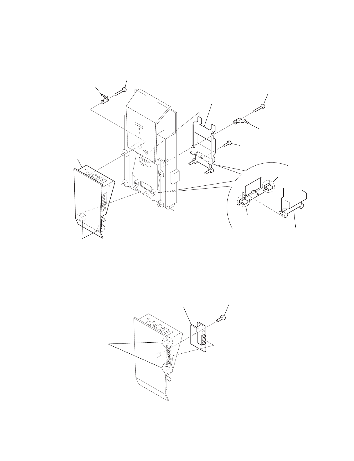
2-15. CONTROL DOOR BLOCK ASSEMBLY
KDP-57XBR2/65XBR2
RM-Y185
7 Door stopper (u)
9 Control door block
assembly
8 Two bosses
6 Screw (+BV 3 x 25)
4 Screw (+BV 3 x 25)
3 DV block bracket
5 Door stopper (u)
1 Screw (+BVTP 3 x 12)
2 Claw
2 Claw
DV block bracket
2-16. HB BOARD REMOVAL
2 Two claws
3 HB board
– 15 –
1 Screw (+BVTP 3 x 12)
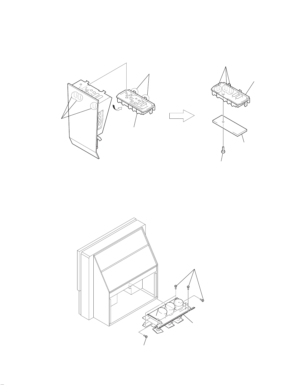
2-17. HA BOARD REMOVAL
1 Three claws
5 Three claws
6 Multi button
7 HA board
2 Two claws
3 Multi button block
4 Screw (+BVTP 3 x 12)
KDP-57XBR2/65XBR2
RM-Y185
2-18. PICTURE TUBE BLOCK REMOVAL
1 Seven screws (HEX tap)
2 Picture tube block
1 Screw (HEX tap)
– 16 –
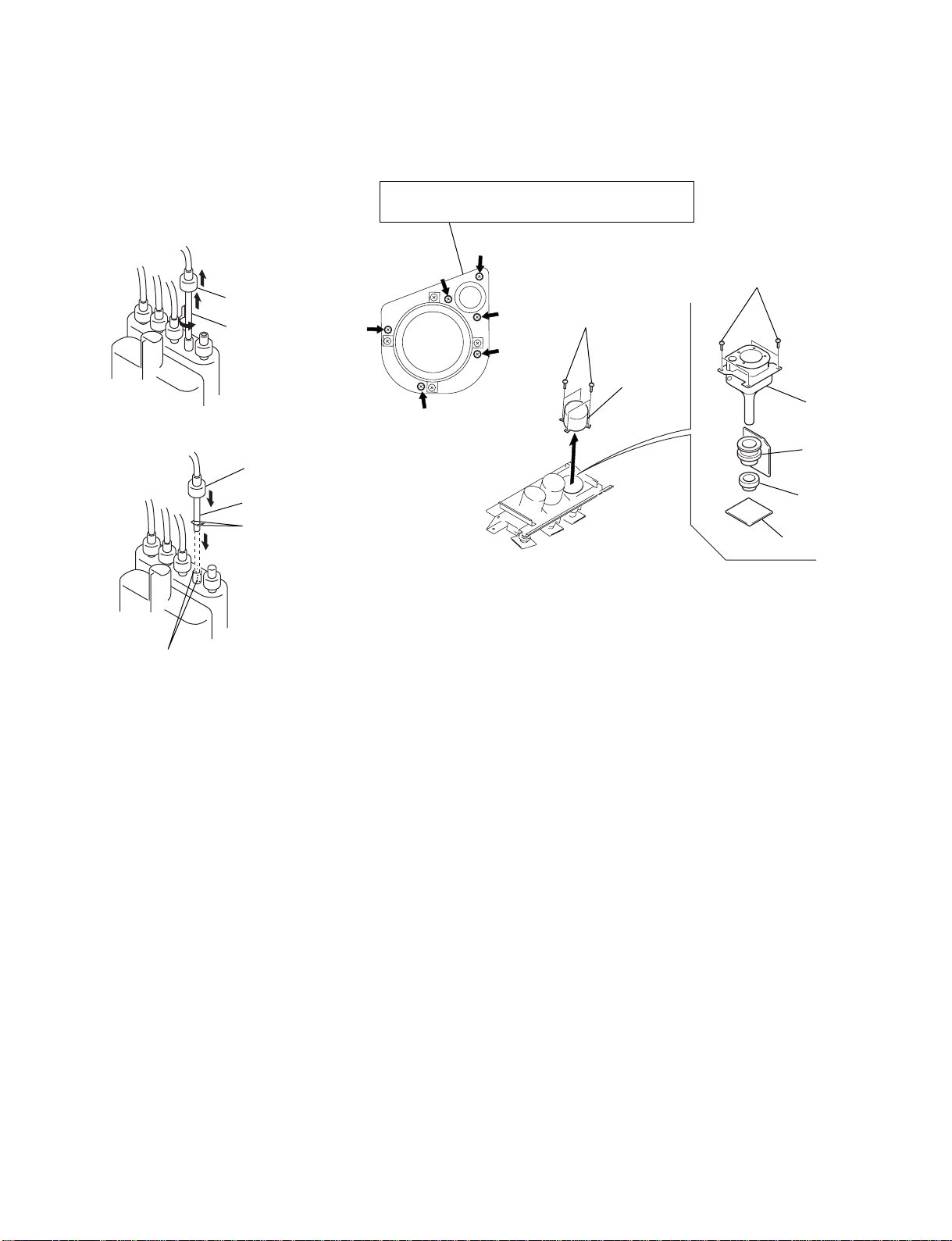
CABLE REMOVAL
AND INSTALLATION
(1) Removal
1 Rubber cap
2 HV cable
turn 90°
(2) Installation
2 Rubber cap
KDP-57XBR2/65XBR2
RM-Y185
2-20. PICTURE TUBE REMOVAL2-19. HIGH-VOLTAGE
Removing the arrow-marked screw is strictly inhibited.
If removed, it may cause liquid spill.
6 Four screws
(+BVTP 4 x 12)
1 Four screws
(HEX TAP 4 x 20)
2 Lens
7 Picture
tube
5 Deflection
yoke
Gutter
1 HV cable
Hook
4 Neck
assembly
3 CR board
– 17 –

SECTION 3
SET-UP ADJUSTMENTS
KDP-57XBR2/65XBR2
K RM-Y185
3-1. SCREEN VOLTAGE ADJUSTMENT
(ROUGH ALIGNMENT)
1. Receive the monoscope signal.
2. Set 50% BRIGHTNESS and minimum PICTURE.
3. Turn the red VR on the focus pack all the way to the left and
then gradually turn it to the right until the point where you
can see the retrace line.
4. Next gradually turn it to the left to the position where the
retrace line disappears.
RG
SCREEN
RG
FOCUS
B
B
Focus Pack
Fig. 3-1
3-2. SCREEN (G2) ADJUSTMENT
Fine Mode is recommended to set screen controls to their optimal condition. It is necessary to build the simple jig, illustrated
below, using 3-watt resistors. Please note, that if the proper voltage is not obtained with their listed values, resistors, then please
increase or decrease one of the values in the resistor network to
obtain the correct voltage.
1. Select VIDEO1 mode without signals.
2. Connect G2 JIG to TP3802 (200V) of CG board and GND.
3. SW on JIG.
4. Connect an oscilloscope to the SG3701(KR), SG3801(KG)
and SG3901(KB) of CR board, CG board and CB board.
5. Adjust R, G and B screen voltage to 175 ± 1V with screen
VR on the focus pack.
3-3. DEFLECTION YOKE TILT ADJUSTMENT
1. Connect the color bar generator monoscope pattern to
VIDEO1 input.
2. Cover the both red and blue picture lenses with the lens caps
to show only the green color.
3. Loosen the deflection yoke set screw and align the tilt of the
Deflection Yoke so that the bars at the center of the
monoscope pattern are horizontal.
4. After aligning the deflection yoke, fasten it securely to the
funnel-shaped portion (neck) of the CRT.
5. The tilt of the deflection yoke for red is aligned in the mode
Cover the both green and blue picture lenses with the lens
caps and the tilt of the deflection yoke for blue is aligned
with in the mode Cover the both green and red picture lenses
with the lens caps is aligned the same as was done for green.
Note: Instead of items 2 and 5, you can cut off the unnecessary
color beams by controlling the service mode “1 RGBS” of
“2150P-2”.
4-pole magnet
2-pole magnet
Centering magnet
Deflection yoke
Anode cap
Fig. 3-3
G2 JIG
TO CG BOARD
TP3802
(200V)
GND
KR, KG, KB
SW
3.3k 5.6k 5.6k 5.6k
All resistors are 3W type
175 ± 1V
pedestal level
Fig. 3-2
GND
– 18 –
KDP-57XBR2/65XBR2
K RM-Y185
3-4. FOCUS LENS ADJUSTMENT
In this adjustment, use the remote commander in the service mode.
For details of the usage of the service mode and the remote commander,
please refer the item 3-10. ELECTRICAL ADJUSTMENT BY
REMOTE COMMANDER.
1. Loosen the lens screw.
2. Cover the both red and blue picture lenses with the lens caps
to show only the green color.
3. Turn the green lens to adjust to the optimum focus point with
the crosshatch signal.
4. Tighten the lens screw.
5. Cover the both green and blue picture lenses with the lens
caps to show only the red color.
6. Adjust red CRT lens just the same as green.
7. Cover the both green and red picture lenses with the lens
caps to show only the blue color.
8. Adjust blue CRT lens just the same as green.
9. After adjusting the items 3-5. FOCUS VR ADJUSTMENT,
3-6. 2-POLE MAGNET ADJUSTMENT, 3-7. CENTER
MAGNET ADJUSTMENT and 3-8. 4-POLE MAGNET
ADJUSTMENT, adjust again to the optimum focus point.
3-5. FOCUS VR ADJUSTMENT
1. Set generator to crosshatch.
2. Cover the both red and blue picture lenses with the lens caps
to show only the green color.
3. Turn the green focus VR on the focus pack to adjust to the
optimum focus point with the crosshatch signal.
4. Cover the both green and blue picture lenses with the lens
caps to show only the red color.
5. Turn the red focus VR on the focus pack to adjust to the
optimum focus point with the crosshatch signal.
6. Cover the both green and red picture lenses with the lens
caps to show only the blue color.
7. Turn the blue focus VR on the focus pack to adjust to the
optimum focus point with the crosshatch signal.
8. After adjusting the items 3-4. FOCUS LENS ADJUSTMENT,
3-6. 2-POLE MAGNET ADJUSTMENT, 3-7. CENTER
MAGNET ADJUSTMENT and 3-8. 4-POLE MAGNET
ADJUSTMENT, adjust again to the optimum focus point.
Note: Instead of items 2, 4 and 6, you can cut off the unneces-
sary color beams by controlling the service mode “1
RGBS” of “2150P-2”.
Note: Instead of items 2, 5 and 7, you can cut off the unneces-
sary color beams by controlling the service mode “1
RGBS” of “2150P-2”.
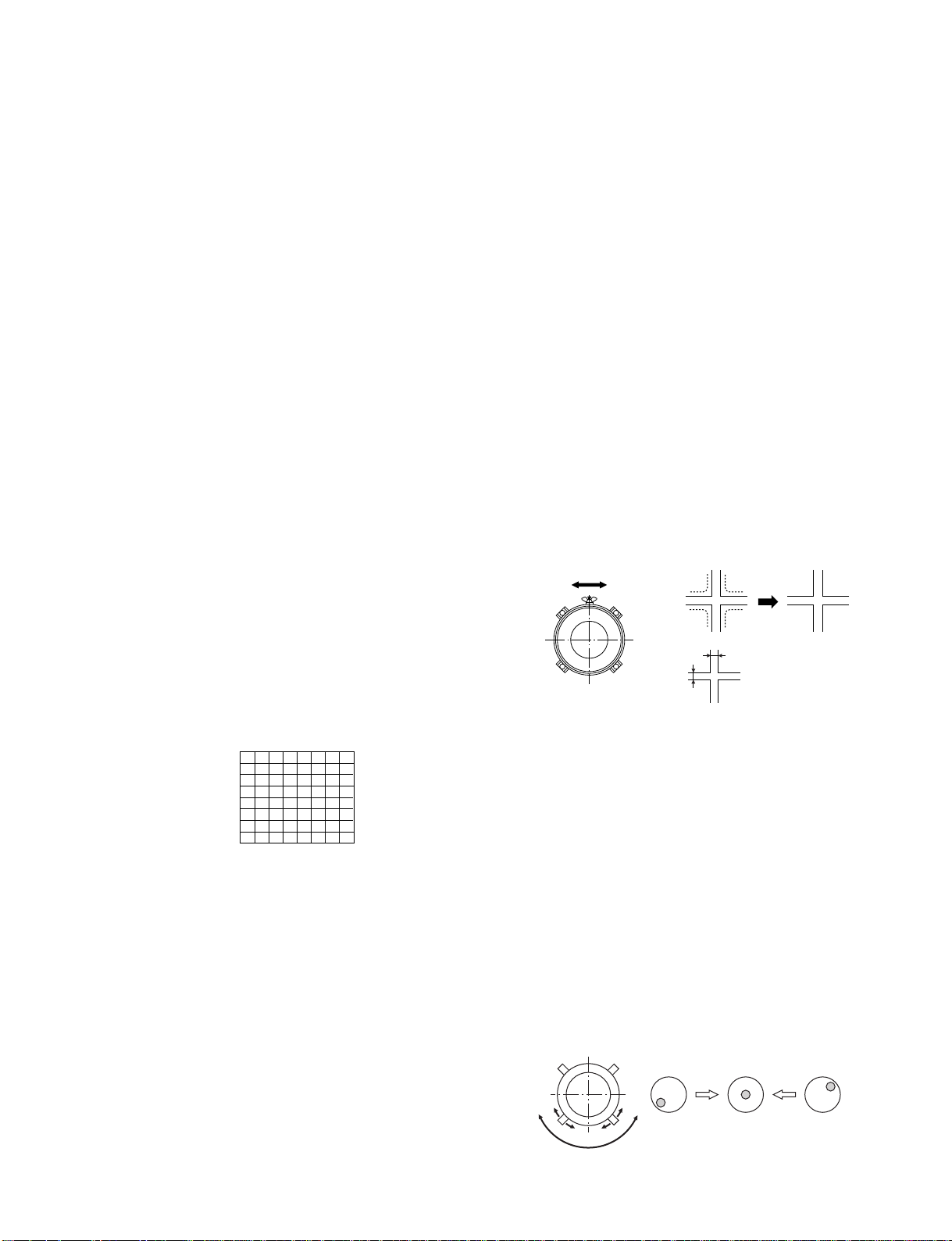
*:Every time you press 6, the test signal changes to
“crosshatch+video signal” “crossbatch+borderline(black)” - “crosshach(black)” “dots(black)” - off.
Test signal
Fig. 3-4
A
Minimize both A and B.
Lens
Fig. 3-5
B
Fig. 3-6
3-6. 2-POLE MAGNET ADJUSTMENT
1. Set the picture mode to“Pro” and picture to MAX.
2. Receive the dot signal.
3. Cover the both red and blue picture lenses with the lens caps
to show only the green color.
4. Turn the green focus VR on the focus pack to the left and set
to overfocus to enlarge the spot.
5. Adjust 2-pole magnet so that the bright spot should be
centered.
6. Align the green focus VR and set for just (precise) focus.
7. Perform the same alignment for red and blue.
Note: Instead of item 2 you can cut off the unnecessary color
beams by controlling the service mode “1 RGBS” of
“2150P-2”.
Use the center dot
– 19 –
Fig. 3-7

KDP-57XBR2/65XBR2
K RM-Y185
3-7. CENTERING MAGNET ADJUSTMENT
1. Set the picture mode to “Pro”.
2. Receive the monoscope signal.
3. Cover the both red and blue picture lenses with the lens caps
to show only the green color.
4. Adjust the green centering magnet to put the center of the
monoscope signal to the center of the screen.
5. Adjust the red centering magnet in the same way.
6. Adjust the blue centering magnet in the same way.
Note: Instead of item 2 you can cut off the unnecessary color
beams by controlling the service mode “1 RGBS” of
“2150P-2”.
3-8. 4-POLE MAGNET ADJUSTMENT
1. Set the picture mode to“Pro” and picture to MAX.
2. Receive the dot signal.
3. Cover the both red and blue picture lenses with the lens caps
to show only the green color.
4. Turn the green focus VR on the focus pack to the right and
set the spot will become smaller.
5. Adjust the 4-Pole Magnet so that the spot becomes round for
green and red.
6. Adjust blue spot to an oval shape. x : y = 1 : 1.2
3-9. DEFOCUS ADJUSTMENT (BLUE)
Note: Please adjust the blue dot to be slightly larger than red and
green dots. This adjustment provides a more pleasing picture to the customer.
1. Select the picture mode to “Pro”.
2. Receive the dot signal.
3. Cover the both red md green picture lenses with the lens caps
to show only the blue color.
4. Turn the blue focus VR on the focus pack to right to make
the round dot elipical.
5. Check flare with high luminace signal, make sure flare is
minimal while dot shape is elipical.
6. Set generdtor to all white signal and check uniformity.
Note: Instead of item 3 you can cut off the unnecessary color
beams by controlling the service mode “1 RGBS” of
“2150P-2”.
Note: Instead of item 2 you can cut off the unnecessary color
beams by controlling the service mode “1 RGBS” of
“2150P-2”.
Use the center dot
[GREEN and RED]
NG
NG
OK
[BLUE]
OK
x
Fig. 3-8
57 inch : 19 to 26 mm
65 inch : 22 to 30 mm
y
x : y = 1 : 1.2
– 20 –
KDP-57XBR2/65XBR2
DISPLAY
JUMP
ADD SURF
SLEEP SAT/CABLE
SAT/CABLE
FUNCTION
MENU
ENTER
VOL
EXIT
IN
D
E
X
G
U
ID
E
PIC MODE
WIDE MODE
TV/VIDEOANT
TV
TV
123
456
7.89
0
MUTING
POWER
FREEZE
RESET
DRC
CINEMOTION
RM-Y185
MTS/SAP
TIMER
CH
F
A
V
O
R
I
T
E
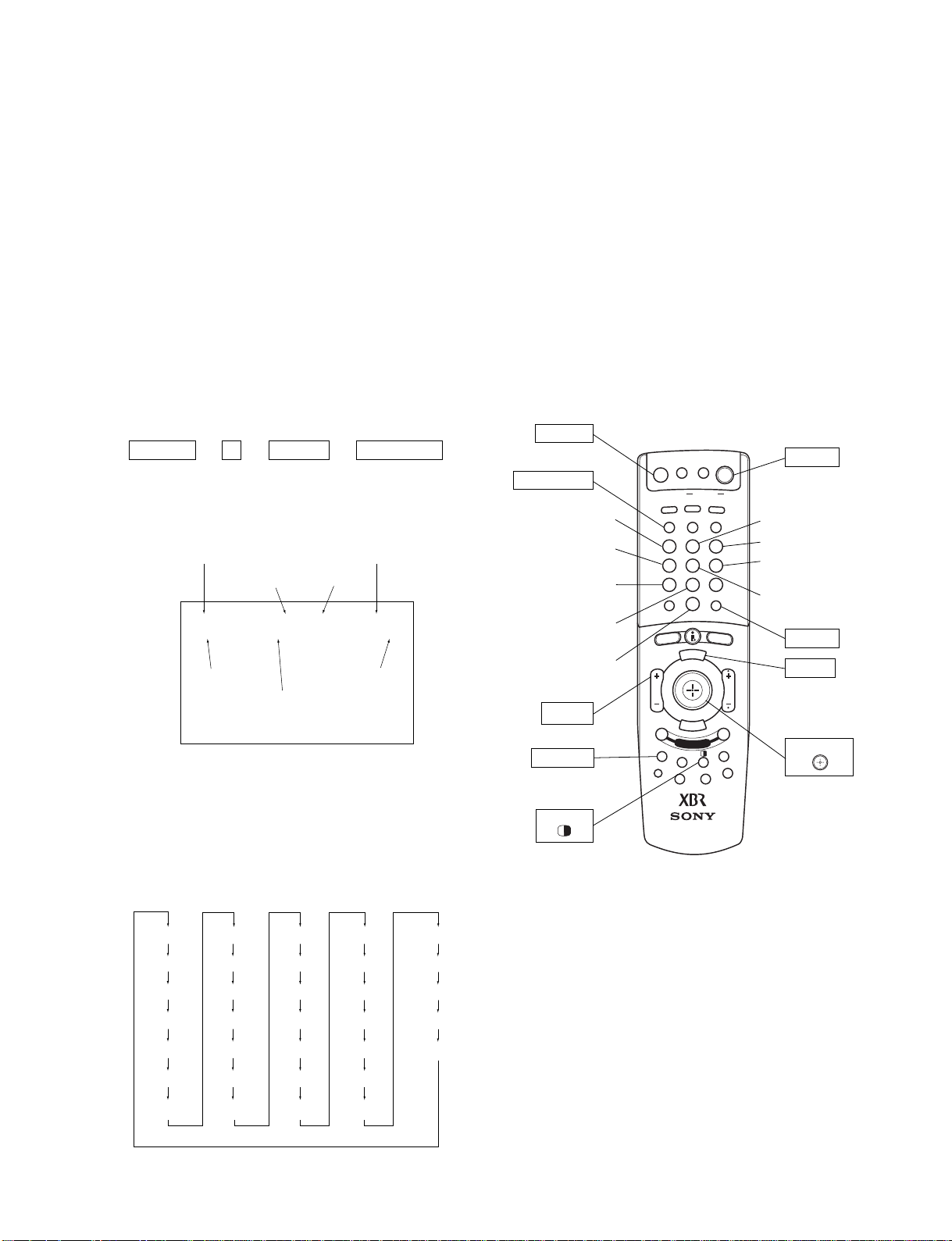
DISPLAY
Adjustment item
up
Adjustment item
down
JOYSTICK
Adjustment category
up
Read data from
NVM
Write data to NVM
POWER
MUTING
VOL +
ENTER
MENU
WIDE MODE
Adjustment category
down
Data up
Move : V,v,B,b
Push : Enter
Data down
TWIN
Initialize data
(Not stored)
User control goes
to the standerd state
RM-Y185
K RM-Y185
3-10. ELECTRICAL ADJUSTMENT BY REMOTE
COMMANDER
By using remote commander (RM-Y185), all circuit adjustments can be made.
NOTE : Test Equipment Required.
1. Pattern Generator (with component outputs)
2. Frequency counter
3. Digital multimeter
4. Audio oscillator
1. Method of Setting the Service Adjustment
Mode
SERVICE MODE PROCEDURE
1. Standby mode. (Power off)
2. DISPLAY t 5 t VOL (+) t TV POWER
on the remote commander.
(Press each button within a second.)
SERVICE MODE ADJUSTMENT
Category Name
Item No.
Mode
Data
7. If you want to recover the latest values press “-” then
“[ENTER]” to read the memory.
8. Press “[MUTING]” then “[ENTER]” to write into memory.
9. Turn power off.
Note: Press “8” then “[ENTER]” on the remote commander to
initialize or turn set off and on to exit.
2. Memory Write Confirmation Method
1. After adjustment, turn power off with the remote commander.
2. Turn power on and set to service mode.
3. Call the adjusted items again and confirm they were adjusted.
3. Adjusting Buttons and Indicator
VERSION 0 0 SERVICE
VER Full TV
Item Name Input Signal
Screen Mode
F/A: 11111111 11111111
CBA: 11111111 11111111
3. The SCREEN displays the item being adjusted.
4. Press “1” or “4” on the remote commander to select the
adjustment item.
5. Press “3” or “ 6” on the remote commander to change the data.
6. Press “2” or “5” on the remote commander to select the category.
Every time you press “2” (Category up), Service mode
changes in the order as shown below.
VERSION
3D-COMB
2103-1
2103-2
2150P-4
2150D-1
2150D-2
2150D-3
2150P-1 D-CONV MID5
2150P-2 CXA2026 CXA3506R
2150P-3 CXA2151 BH3868
MID1
MID2
MID3
MID4
TDA7312F
TDA7312R
TDA7312C
* : GRN , RED or BLU
SNNR
CCD
DTV
TP
PJE (00 FDIS)
PJE (44 COGV)
GRN* (CENT)
OP
ID
Note : When the PJE mode is activated, which displays an inter-
nally generated signal, several buttons on the remote
commander will have different functions than listed
above. Therefore, when in the PJE mode, refer to page 41
for button functions.
– 21 –
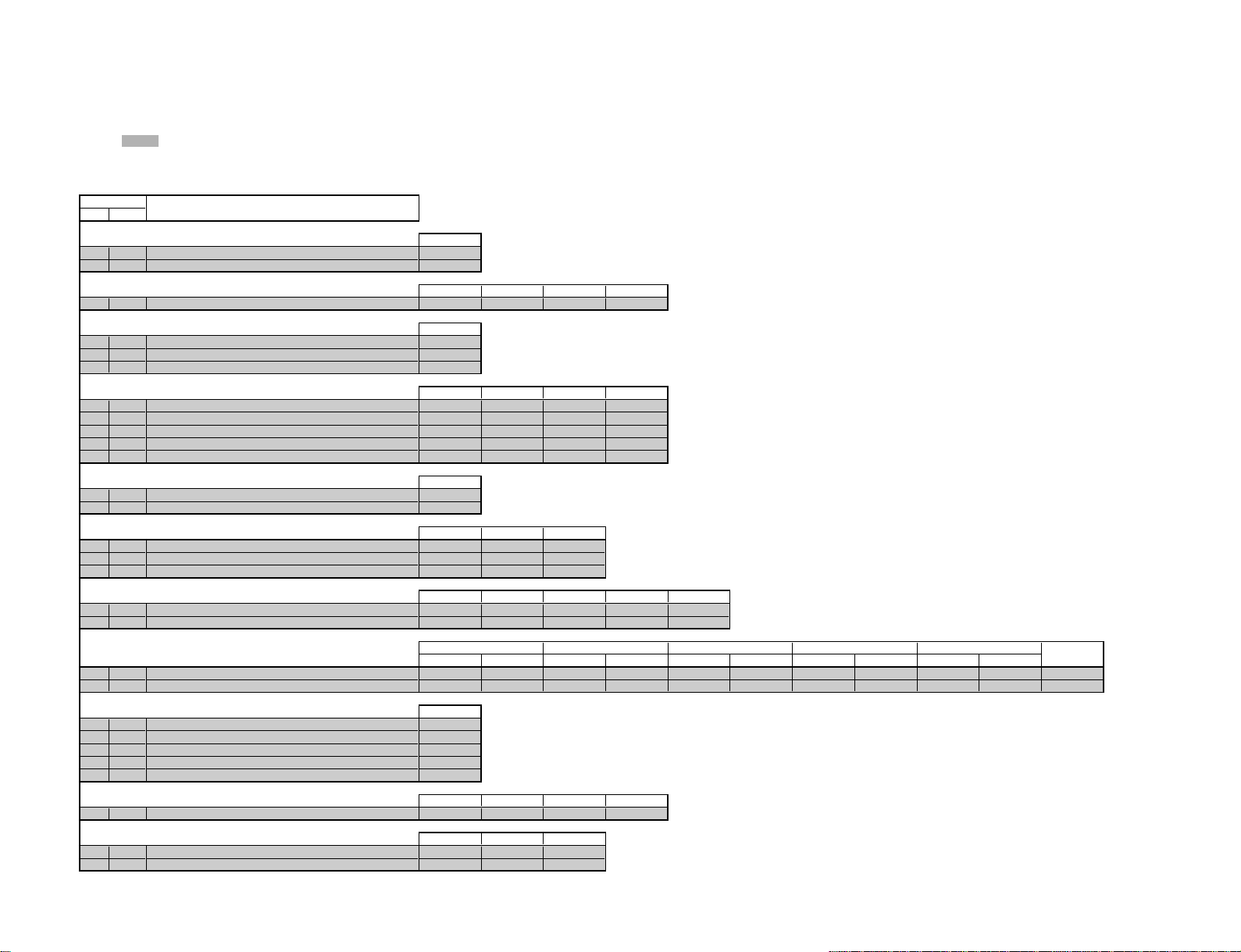
4. Service Mode List
Note: • shaded items are fixed. There is no need to change data. Others are different a little
in the sets individually. Basically, there is no need to change data, too.
3D-COMB
3D Comb Filter (µPD64082)
Item
No. Name
0 NRMD Noise reduction mode [0: YCS, 1: YCS+, 2: MNNR, 3: YCNR] 0
1 YAPS Y aperture/peaking [0: OFF, 1: A-ON, 2: D-ON, 3: A/D-ON] 3
2 CLKS System CLK [0: Auto, 1: Forced-Burst, 2/3: Forced-H freq.] 1111
3 NSDS Signal [0: Auto, 1: F-ST, 2: F-nonST (H), 2/3: F-nonST(V)] 3
4 MSS Processing [0: Auto, 1: F-Inter Frame, 2/3: F-InterLine] 0
5 KILS Color Killer [0: Auto, 1: Port Cont., 2/3: F-Killer] 2
6 CDL Chroma delay time [0: –280 ns, 4: 0 ns, 7: +210 ns] 3333
7 DYCO Y coring level [0: Coring 0, 15: Large amount of Coring] 2222
8 DYGA Y coring gain [0: 0 gain, 15: Maximum gain] 11 11 11 11
9 DCCO C coring level [0: Coring 0, 15: Large amount of Coring] 4444
10 DCGA C coring gain [0: 0 gain, 15: Maximum gain] 8888
– 22 –
11 YNRL YNR limit [0: YNR off (0LSB), 3: YNR 3LSB] 1
12 CNRL CNR limit [0: CNR off (0LSB), 3: CNR 3LSB] 1
13 VTRH H hysteresis of nonST signal det. [0: Hys-off, 3: Hys-high] 1 1 1
14 VTRR H sensitivity of nonST signal det. [0: High, 3: Off] 1 1 1
15 LDSR Frame sensitivity of nonST signal det. [0: High, 3: Off] 2 2 2
16 VAPG Vertical aperture gain [0: Off, 7: Maximum] 00000
17 VAPI Vertical aperture conv. point [0: Off, 31: Max correction] 00000
18 YPFT Y peaking freq. [0: 3.58 MHz, 1: 3.86 MHz, 2: 4.08 MHz, 3: 4.22 MHz] 33333333333
19 YPFG Y peaking gain [0: –1 times, 8: 0 times, 15: +0.875 times] 75757575757
20 YHCO Y coring for y [0: Off, 1: Small, 2: Mid, 3: Large] 0
21 YHCG Y coring gain for High frequency [0: Normal, 1: 0.5 gain] 1
22 HSSL Horizontal sync slice level [0: 4LSB, 15: 19LSB] 12
23 VSSL Vertical sync slice level [0: HSSL+0 LSB, 15: HSSL+15 LSB] 8
24 ADCL ADC clock delay [0: 0 ns, 1: 3 ns, 2: 17.5 ns, 3: 20.5 ns] 3
25 D2GA Motion detect gain 4444
26 SEDY Select DY detect [0: Low sensitivity, 1: High sensitivity] 1 1 1
27 SEDC Select DC detect [0: Low sensitivity, 1: High sensitivity] 0 0 0
Depends on NRMD data
Depends on NRMD data
Depends on Signal Input
Depends on Picture Pallete
Depends on Picture Pallete and Video Input
Depends on NRMD data
Depends on Signal Input
Function
Common
NRMD (0) NRMD (1) NRMD (2) NRMD (3)
Common
NRMD (0) NRMD (1) NRMD (2) NRMD (3)
Common
RF CV/YC
Vivid Standard Movie Game Pro
Vivid Standard Movie Game Pro
RF CV/YC RF CV/YC RF CV/YC RF CV/YC RF CV/YC
Common
NRMD (0) NRMD (1) NRMD (2) NRMD (3)
RF CV/YC
Video5/Video6
Video5/Video6
TWIN
Any
K RM-Y185
KDP-57XBR2/65XBR2
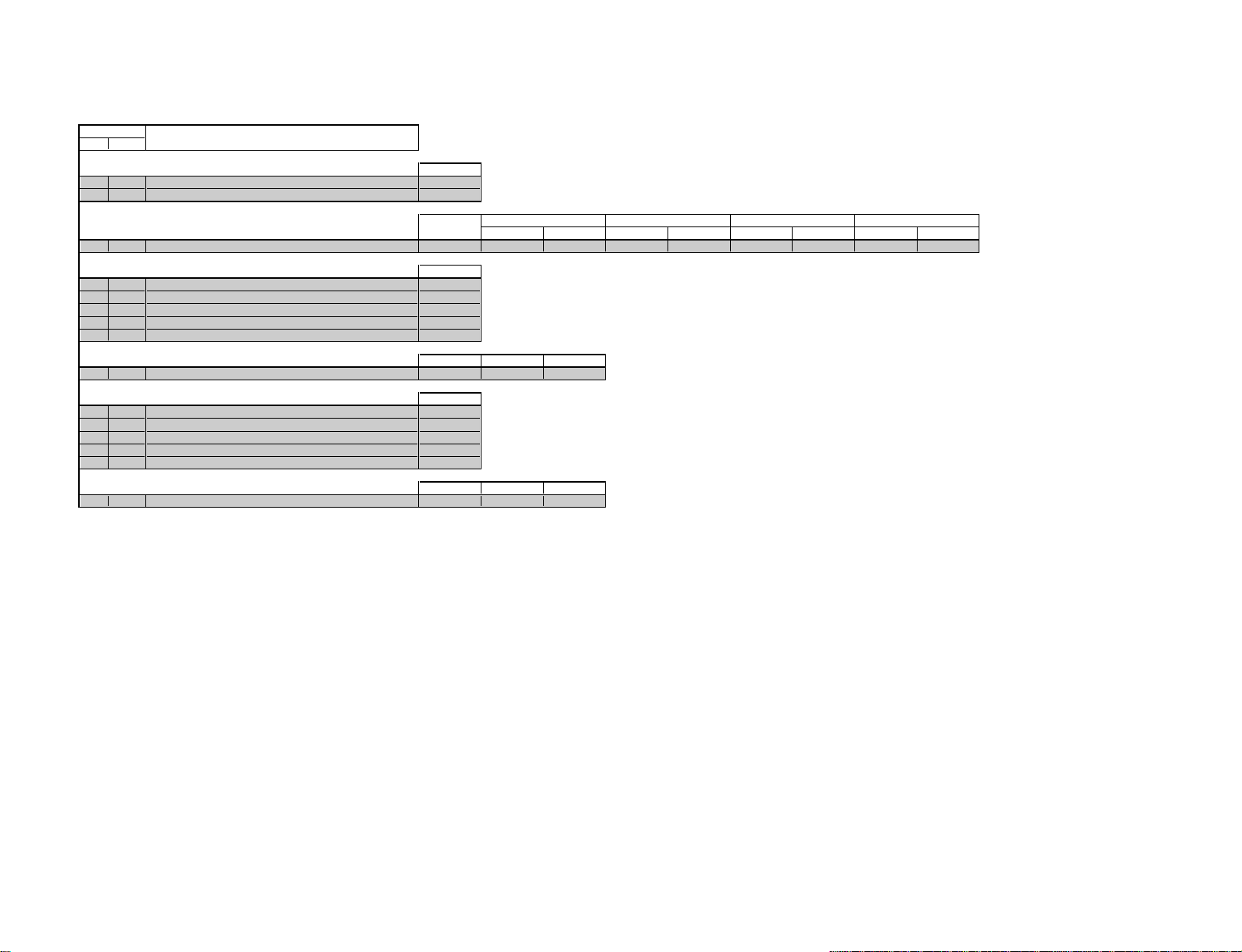
3D Comb Filter (µPD64082)
Item
No. Name
28 KILR Killer detector [0: Off, 1: Low sensitivity, 15: High sensitivity] 3
29 OP NRMD for Y/C input [0: Recursive Type, 1: Comb Type] 1
30 NR1 Initial setting of NR On/Off [0: On, 1: Off] 000000000
31 NR2 S/N adaptive processing [0: On, 1: Off] 0
32 HPLL H PLL filter [0: Slow convergence, 1: Quick convegence 1
33 BPLL Burst PLL filter [0: Quick convergence, 1: Slow convergence] 1
34 FSCF Burst extraction gain [0: High gain, 1: Low gain] 0
35 PLLF PLL loop gain [0: Low gain, 1: High gain] 1
36 CC3N C filter characteristic of comb filter [0: Narrow, 1: Wide] 0 0 0
37 HDP Horizontal phase [0: –1.12 µs, 4: 0 µs, 7: +0.84 µs] 5
38 BGPS Burst gate start [0: HS center +2 µs, 15: HS center +5.75 µs] 4
39 BGPW Burst gate width [0: 0.5 µs, 15: 4.25 µs] 10
40 TEST Test bit [0: Normal, 1: Test mode] 0
41 WSC Noise det. coring [0: 0LSB, 1: 1LSB, 2: 2LSB, 3: 3LSB] 1
– 23 –
42 LIND 262P detect [xx1: nonST H, x1x: nonST V, 1xx: LD still] 0 0 2
Depends on Signal Input
Depends on Signal Input
Depends on Signal Input
Function
Common
RF CV YC CV YC CV YC CV YC
Common
RF CV/YC
Common
RF CV/YC
V1 V2 V3 V4
Video5/Video6
Video5/Video6
K RM-Y185
KDP-57XBR2/65XBR2
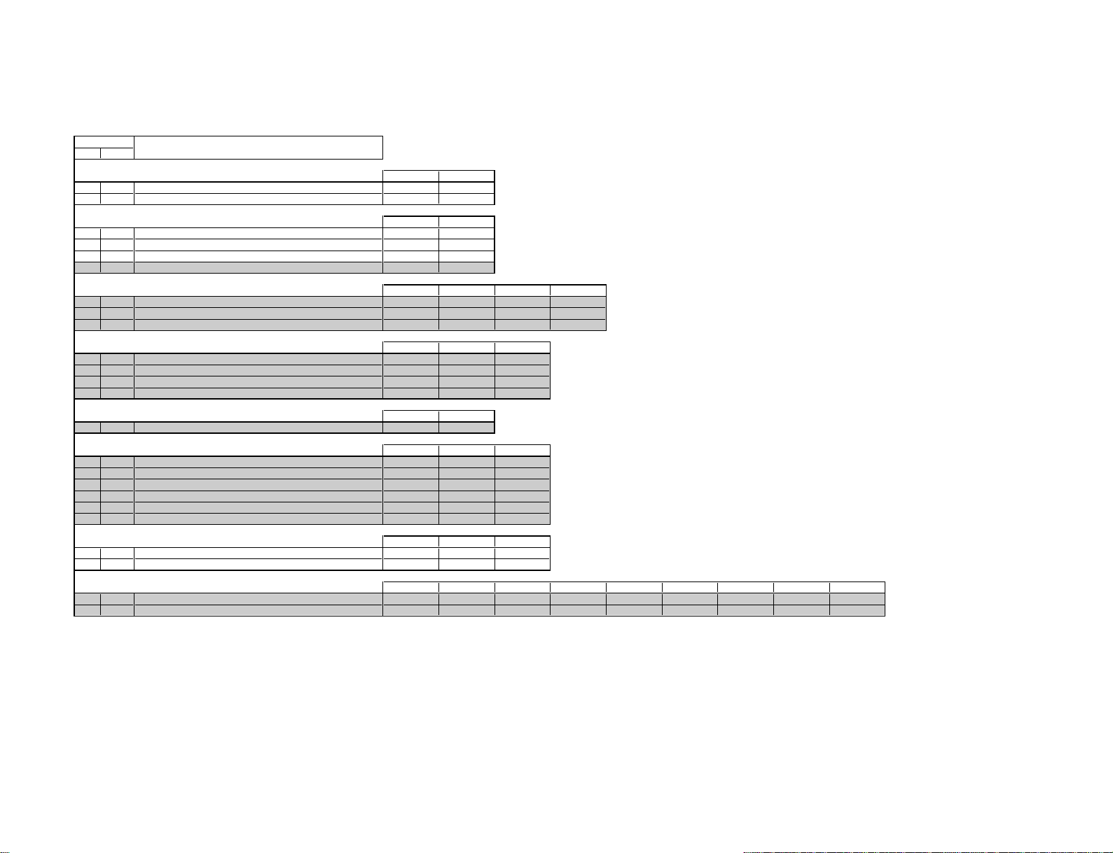
2103-1
Main Chroma Decoder (CXA2103)
Item
No. Name
0 YLEV Y out level gain [0: 2.9 dB, 63: 9.0 dB] 35 35
1 CLEV CbCr out level gain [0: 2.9 dB, 63: 9.0 dB] 50 42
2 SCON Sub contrast [0: –2 dB, 15: +2 dB] 9 9
3 SCOL Sub color [0: –2 dB, 15: +2 dB] 2 2
4 SHUE Sub hue [0: –8.8 deg, 15: +8.8 deg] 11 5
5 YDLY Y/C delay [0: Ref, 1: 30 ns Y delay, 2: 60 ns, 3: 100 ns] 0 0
6 SHAP Sharpness [0: –3 dB, 15: +3 db] 6884
7 SHFO Sharpness F0 [0: 2.5 MHz, 1: 3.0 MHz, 2: 3.5 MHz, 3: 4.0 MHz] 0003
8 PREO Pre-over ratio [0: 1.5:1, 1: 1:1, 2: 1:1.5, 3: 1:2] 3333
9 BPFO Chroma BPF F0 [0: fsc, 1: fsc+400 kHz, 2: fsc+800 kHz, 3: fsc+1.2 MHz] 3 0 0
10 BFFQ Chroma BPF Q [0: 2.0, 1: 1.5, 2: 1.2, 3: 1.0] 0 3 3
11 BPSW Chroma BPF On/Off [0: Off, 1: On] 1 0 0
12 TRAP Chroma trap on Y On/Off [0: Off, 1: On] 0 0 0
– 24 –
13 LPF Output LPF (YCbCr) [0: On, 1: Off (through)] 1 0
14 AFCG PLL loop gain [0: fast, 1: slow] 1 0 0
15 CDMD
16 SSMD Slice level [0: auto, 1: HV 65%, 2: H 25% V 65%, 3: HV 25%] 0 0 0
17 HMSK Mask for Macro Vision [0: Off, 1: On] 0 1 1
18 HALI Auto H alignment [0: Off, 1: On (AFC free run)] 0 0 0
19 PPHA Picture/H Tim phase [0: –0.5 µs, 15: +0.5 µs] 777
20 CBOF Cb/Ext Cb offset [0: –16 mV, 63: +16 mV] 26 29 25
21 CROF Cr/Ext Cr offset [0: –16 mV, 63: +16 mV] 23 30 25
ATPD Auto pedestal point [0: Through, 1: 20 IRE, 2: 30 IRE, 3: 40 IRE] 001222231
**22
DCTR DC transfer ratio [0: 100%, 1: 85%, 2: 90%, 3: 85%] 002113322
**23
Function
Depends on Signal Path
Depends on Signal Input
Depends on Signal Input
Depends on Signal Input
Depends on Signal Path
Depends on Signal Input
Count down mode [0/1/3: CountDown, 2: H look *
Depends on Signal Input
Depends on CXA2150P-4 BLK
** Main and Sub CXA2103 share the same data for items 22 and 23.
Tc: 0>1>3]
DRC VDO
RF CV/YC
RF CV YC Video5
RF CV YC
DRC VDO
RF CV/YC
333
RF Video5 Video6
Single BLK (0) BLK (1) BLK (2) BLK (3) BLK (4) BLK (5) BLK (6) BLK (7)
Video5/Video6
K RM-Y185
KDP-57XBR2/65XBR2
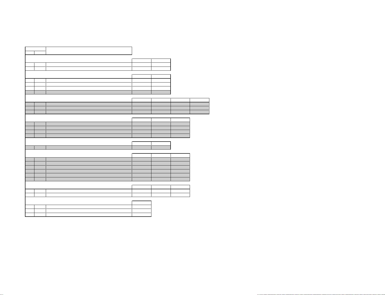
2103-2
Sub Chroma Decoder (CXA2103)
Item
No. Name
0 YLEV Y out level gain [0: 2.9 dB, 63: 9.0 dB] 35 35
1 CLEV CbCr out level gain [0: 2.9 dB, 63: 9.0 dB] 50 42
2 SCON Sub contrast [0: –2 dB, 15: +2 dB] 8 8
3 SCOL Sub color [0: –2 dB, 15: +2 dB] 3 3
4 SHUE Sub hue [0: –8.8 deg, 15: +8.8 deg] 10 3
5 YDLY Y/C delay [0: Ref, 1: 30 ns Y delay, 2: 60 ns, 3: 100 ns] 0 0
6 SHAP Sharpness [0: –3 dB, 15: +3 db] 0884
7 SHFO Sharpness F0 [0: 2.5 MHz, 1: 3.0 MHz, 2: 3.5 MHz, 3: 4.0 MHz] 0003
8 PREO Pre-over ratio [0: 1.5:1, 1: 1:1, 2: 1:1.5, 3: 1:2] 3333
9 BPFO Chroma BPF F0 [0: fsc, 1: fsc+400 kHz, 2: fsc+800 kHz, 3: fsc+1.2 MHz] 0 0 0
10 BPFQ Chroma BPF Q [0: 2.0, 1: 1.5, 2: 1.2, 3: 1.0] 3 3 3
11 BPSW Chroma BPF On/Off [0: Off, 1: On] 0 1 1
12 TRAP Chroma trap on Y On/Off [0: Off, 1: On] 0 0 0
– 25 –
13 LPF Output LPF (YCbCr) [0: On, 1: Off (through)] 1 0
14 AFCG PLL loop gain [0: fast, 1: slow] 1 0 0
15 CDMD
16 SSMD Slice level [0: auto, 1: HV 65%, 2: H 25% V 65%, 3: HV 25%] 0 0 0
17 HMSK Mask for Macro Vision [0: Off, 1: On] 0 1 1
18 HALI Auto H alignment [0: Off, 1: On (AFC free run)] 0 0 0
19 PPHA Picture/H Tim phase [0: –0.5 µs, 15: +0.5 µs] 777
20 CBOF Cb/Ext Cb offset [0: –16 mV, 63: +16 mV] 27 31 31
21 CROF Cr/Ext Cr offset [0: –16 mV, 63: +16 mV] 22 31 31
22 2SCO SCON offset of CV for 2H Conb [0: –7step, 7: ±0step, 15: +8step] 7
23 2SCL SCOL offset of CV for 2H Conb [0: –7step, 7: ±0step, 15: +8step] 7
24 2SHU SHUE offset of CV for 2H Conb [0: –7step, 7: ±0step, 15: +8step] 7
Function
Depends on Signal Path
Depends on Signal Input
Depends on Signal Input
Depends on Signal Input
Depends on Signal Path
Depends on Signal Input
Count down mode [0/1/3: CountDown, 2: H look *Tc: 0>1>3]
Depends on Signal Input
DRC VDO
RF CV/YC
RF CV YC Video5
RF CV YC
DRC VDO
RF CV/YC
333
RF Video5 Video6
Common
Video5/Video6
K RM-Y185
KDP-57XBR2/65XBR2
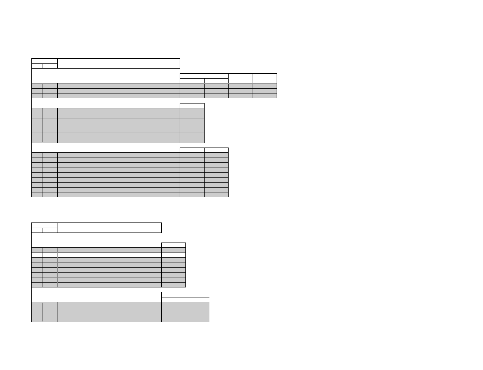
2150P-1
Video Processor (CXA2150)
Item
No. Name
0 YOF Y offset [0: –39 mV, 7: 0 mV, 15: +45 mV] 7 7 7 7
1 CBOF Cb offset [0: B –36 mV G +16 mV, 31: B 0 mV G 0 mV, 63: B +43 mV G –20 mV] 31 37 28 40
2 CROF Cr offset [0: R –46 mV G +10 mV, 31: R 0 mV G 0 mV, 63: R +55 mV G –12 mV] 31 37 28 40
3 SBRT Sub brightness [0: –15 IRE, 31: 0 IRE, 63: 15 IRE] 31
4 RDRV R drive gain [0: –4 dB, 41: 0 dB, 63: +2 dB] 39
5 GDRV G drive gain [0: –4 dB, 41: 0 dB, 63: +2 dB] 39
6 BDRV B drive gain [0: –4 dB, 41: 0 dB, 63: +2 dB] 39
7 RCUT R cut-off [0: –9 dB, 31: 0 dB, 63: +4 dB] 31
8 GCUT G cut-off [0: –9 dB, 31: 0 dB, 63: +4 dB] 31
9 BCUT B cut-off [0: –9 dB, 31: 0 dB, 63: +4 dB] 31
10 WBSW White balance offset [0: Normal, 1: R 100% G 90% B 70%] 0 0
11 SBOF Sub brightness offset color temperature [0: –7, 7: 0, 15: +8] 7 7
12 RDOF RDRV offset [0: –15, 15: 0, 31: +16] 15 15
13 GDOF GDRV offset [0: –15, 15: 0, 31: +16] 15 15
14 BDOF BDRV offset [0: –15, 15: 0, 31: +16] 15 15
– 26 –
15 RCOF RCUT offset [0: –15, 15: 0, 31: +16] 15 15
16 GCOF GCUT offset [0: –15, 15: 0, 31: +16] 15 15
17 BCOF BCUT offset [0: –15, 15: 0, 31: +16] 15 15
18 DCOL Dynamic color, Cool [0: Off, 1: High (2025), 2: Mid (2100), 3: Low] 3 --
2150P-2
Video Processor (CXA2150)
Item
No. Name
Depends on Signal Path and Source
Depends on Color Temperature
Function
Function
Analog *1 Used when a 1080i signal by-passes the MID
1080i *1 other *2
Common
Warm Cool
DTV TWIN
*2 Used for Analog signals passing through the MID
0 ALBK Picture + Ref. Pulse on/off for G2 adjustment [0: RGB off, 1: RGB on] 1
1 RGBS [0: All off, 1: B, 2: G, 3: BG, 4: R, 5: BR, 6: GR, 7:BGR] 7
2 BLKB Bottom limiter level [Ref. Pulse DC voltage 0: –1.25, 3: –0.65] 3
3 LIML RGB limiter level [0: 115 IRE, 1: 123 IRE, 2: 131 IRE, 3: 140 IRE] 0
4 PABL Peak ABL [0: 4.9 Vdc, 15: 6.8 Vdc] 15
5 SABL Signal ABL level [0: Off, 3: maximum gain] 0
6 AGNG Black/White aging [0: Normal, 1: Black, 2: White, 3: Inhibit] 0
7 AKBO AKB on/off [0: On, 1: Off] 0
Depends on Signal Format
8 SYPH H sync delay [0: 0%, 1: –3.125%] 0 0
9 CLPH Clamp pulse phase [0: +5%, 1: +4%, 2: +1%, 3: +2%] 2 2
10 CLGA Clamp gate on/off [0: Not gated, 1: Gated with input H sync] 0 0
11 CLSH Clamp pulse start shift [0: No shift, 1: –3.125% shift from CLPH] 0 0
Common
Analog *1 Used when a 1080i signal by-passes the MID
*1
1080i
other
*2 Used for Analog signals passing through the MID
*2
K RM-Y185
KDP-57XBR2/65XBR2
2150P-3
Video Processor (CXA2150)
No. Name
0 SYSM Bandwidth [0: NTSC, 1: FF, 2: HD, 3: DTV] 1 1 1 1 3 3 1 1 3 3 2
1 VMLV VM level [0: VM0, 1: VM1, 2: VM2, 3: VM3, 4: VM4, 5: VM5, 6: VM6, 7: VM7] 7 7 7 7 7 7 7 7 7 7 7
2 VMMO VM mode (VM_LEV) [0: Off, 1: Low, 2: Mid, 3: High] 3 3 3 3 3 3 3 3 3 3 3
3 VMCR VM coring level [0: Off, 1: ±5%, 2: ±10%, 3: ±15%] 1 0 0 0 0 0 0 0 0 0 1
4 VMLM VM limiter level [0: Off, 1: ±83%, 2: ±67%, 3: ±50%] 0 0 0 0 0 0 0 0 0 0 0
5 VMF0 VM f0 [0: Low, 1: Mid, 2: High, 3: Inhibit] 1 1 1 1 2 2 1 1 2 2 0
6 VMDL VM delay [0: Short, 3: Long] 1 1 1 1 0 0 1 1 0 0 2
7 SHOF Sharpness offset [0: 0step, 1: +4step, 2: +8step, 3: +12step] 3 1 1 0 2 2 0 0 2 2 0
8 SHF0 Sharpness f0 [0: Low, 1: Mid, 2: High, 3: Inhibit] 1 1 1 1 1 1 1 1 1 1 1
9 PROV Pre-over ratio [0: 1:1.5, 1: 1:1, 2: 1.5:1, 3: 2:1] 3 3 3 3 3 3 3 3 3 3 2
10 F1LV Sharpness f1 [0: 0 dB, 1: +1 dB, 2: +2 dB, 3: +3 dB] 0 0 0 0 3 3 0 0 3 3 0
11 CDSP Sharpness at color high [0: 0 dB, 1: +2 dB, 2: +4 dB, 3: +6 dB] 0 0 0 0 0 0 0 0 0 0 0
12 LTLV LTI level [0: Off, 1: Low, 2: Mid, 3: High] 3 3 3 3 3 3 3 3 3 3 3
13 LTMD LTI mode [0: for Black & White, 1: for Black, 2: for White, 3: Inhibit] 1 1 1 1 1 1 1 1 1 1 0
14 CTLV CTI level [0: Off, 1: Low, 2: Mid, 3: High] 0 0 0 0 0 0 0 0 0 0 0
15 CTMD CTI mode [0: for Black & White, 1: for Black, 2: for White, 3: Inhibit] 0 0 0 0 0 0 0 0 0 0 0
16 UBOF User bright offset [0: BRIGHT +0, ..., 3: BRIGHT +6, ..., 7: BRIGHT +14] 2 2 3 3 0 2 2 2 2 2 0
17 UCOF User color offset [0: COLOR +0, ..., 3: COLOR +6, ..., 7: COLOR +14] 0 0 0 0 0 0 0 0 0 0 0
– 27 –
18 UHOF User hue offset [0: HUE +0, 1: HUE +1, 2: HUE +2, 3: HUE +3] 2 2 2 2 2 2 2 2 2 2 2
19 MIDE MID Enhancement setting table [0: Soft, ..., 63: Sharp] 7 12 17 22 27 32 37 42 47 52 57
0 SYSM Bandwidth [0: NTSC, 1: FF, 2: HD, 3: DTV] 1 1 1 1 3 3 1 1 3 3 2
1 VMLV VM level [0: VM0, 1: VM1, 2: VM2, 3: VM3, 4: VM4, 5: VM5, 6: VM6, 7: VM7] 7 7 7 7 7 7 7 7 7 7 7
2 VMMO VM mode (VM_LEV) [0: Off, 1: Low, 2: Mid, 3: High] 3 3 3 3 3 3 3 3 3 3 3
3 VMCR VM coring level [0: Off, 1: ±5%, 2: ±10%, 3: ±15%] 1 0 0 0 0 0 0 0 0 0 1
4 VMLM VM limiter level [0: Off, 1: ±83%, 2: ±67%, 3: ±50%] 0 0 0 0 0 0 0 0 0 0 0
5 VMF0 VM f0 [0: Low, 1: Mid, 2: High, 3: Inhibit] 1 1 1 1 2 2 1 1 2 2 0
6 VMDL VM delay [0: Short, 3: Long] 1 1 1 1 0 0 1 1 0 0 2
7 SHOF Sharpness offset [0: 0step, 1: +4step, 2: +8step, 3: +12step] 2 2 2 0 2 3 0 0 2 3 0
8 SHF0 Sharpness f0 [0: Low, 1: Mid, 2: High, 3: Inhibit] 1 1 1 1 1 1 1 1 1 1 1
9 PROV Pre-over ratio [0: 1:1.5, 1: 1:1, 2: 1.5:1, 3: 2:1] 3 3 3 3 3 3 3 3 3 3 2
10 F1LV Sharpness f1 [0: 0 dB, 1: +1 dB, 2: +2 dB, 3: +3 dB] 0 0 0 0 3 3 0 0 3 3 0
11 CDSP Sharpness at color high [0: 0 dB, 1: +2 dB, 2: +4 dB, 3: +6 dB] 0 0 0 0 0 0 0 0 0 0 0
12 LTLV LTI level [0: Off, 1: Low, 2: Mid, 3: High] 2 2 3 3 3 3 3 3 3 3 3
13 LTMD LTI mode [0: for Black & White, 1: for Black, 2: for White, 3: Inhibit] 1 1 1 1 1 1 1 1 1 1 0
14 CTLV CTI level [0: Off, 1: Low, 2: Mid, 3: High] 0 0 0 0 0 0 0 0 0 0 0
15 CTMD CTI mode [0: for Black & White, 1: for Black, 2: for White, 3: Inhibit] 0 0 0 0 0 0 0 0 0 0 0
16 UBOF User bright offset [0: BRIGHT +0, ..., 3: BRIGHT +6, ..., 7: BRIGHT +14] 3 3 5 5 7 6 7 7 7 6 2
17 UCOF User color offset [0: COLOR +0, ..., 3: COLOR +6, ..., 7: COLOR +14] 0 0 0 0 0 0 0 0 0 0 0
18 UHOF User hue offset [0: HUE +0, 1: HUE +1, 2: HUE +2, 3: HUE +3] 2 2 2 2 2 2 2 2 2 2 2
19 MIDE MID Enhancement setting table [0: Soft, ..., 63: Sharp] 5 11 16 21 26 31 36 41 46 51 56
Item
Depends on Signal Format and Picture Pallet
Depends on Signal Format and Picture Pallet
Function
RF CV/YC
RF CV/YC
Component DTV
Vivid Mode
480i 480p 1080i 720p 480i 480p 1080i 720p
Standard Mode
Component DTV
480i 480p 1080i 720p 480i 480p 1080i 720p
TWIN
TWIN
K RM-Y185
KDP-57XBR2/65XBR2
Video Processor (CXA2150)
No. Name
0 SYSM Bandwidth [0: NTSC, 1: FF, 2: HD, 3: DTV] 1 1 1 1 3 3 1 1 3 3 2
1 VMLV VM level [0: VM0, 1: VM1, 2: VM2, 3: VM3, 4: VM4, 5: VM5, 6: VM6, 7: VM7] 2 2 2 2 2 2 2 2 2 2 2
2 VMMO VM mode (VM_LEV) [0: Off, 1: Low, 2: Mid, 3: High] 3 3 3 3 3 3 3 3 3 3 3
3 VMCR VM coring level [0: Off, 1: ±5%, 2: ±10%, 3: ±15%] 1 0 0 0 0 0 0 0 0 0 1
4 VMLM VM limiter level [0: Off, 1: ±83%, 2: ±67%, 3: ±50%] 0 0 0 0 0 0 0 0 0 0 0
5 VMF0 VM f0 [0: Low, 1: Mid, 2: High, 3: Inhibit] 1 1 1 1 2 2 1 1 2 2 0
6 VMDL VM delay [0: Short, 3: Long] 1 1 1 1 0 0 1 1 0 0 2
7 SHOF Sharpness offset [0: 0step, 1: +4step, 2: +8step, 3: +12step] 0 0 1 0 2 0 0 0 2 0 0
8 SHF0 Sharpness f0 [0: Low, 1: Mid, 2: High, 3: Inhibit] 1 1 1 1 1 1 1 1 1 1 1
9 PROV Pre-over ratio [0: 1:1.5, 1: 1:1, 2: 1.5:1, 3: 2:1] 3 3 3 3 3 3 3 3 3 3 2
10 F1LV Sharpness f1 [0: 0 dB, 1: +1 dB, 2: +2 dB, 3: +3 dB] 0 0 0 0 3 3 0 0 3 3 0
11 CDSP Sharpness at color high [0: 0 dB, 1: +2 dB, 2: +4 dB, 3: +6 dB] 0 0 0 0 0 0 0 0 0 0 0
12 LTLV LTI level [0: Off, 1: Low, 2: Mid, 3: High] 1 1 1 1 1 1 1 1 1 1 1
13 LTMD LTI mode [0: for Black & White, 1: for Black, 2: for White, 3: Inhibit] 0 0 0 0 0 0 0 0 0 0 0
14 CTLV CTI level [0: Off, 1: Low, 2: Mid, 3: High] 0 0 0 0 0 0 0 0 0 0 0
15 CTMD CTI mode [0: for Black & White, 1: for Black, 2: for White, 3: Inhibit] 0 0 0 0 0 0 0 0 0 0 0
16 UBOF User bright offset [0: BRIGHT +0, ..., 3: BRIGHT +6, ..., 7: BRIGHT +14] 6 6 3 3 3 3 3 3 3 3 4
17 UCOF User color offset [0: COLOR +0, ..., 3: COLOR +6, ..., 7: COLOR +14] 0 0 0 0 0 0 0 0 0 0 0
18 UHOF User hue offset [0: HUE +0, 1: HUE +1, 2: HUE +2, 3: HUE +3] 2 2 2 2 2 2 2 2 2 2 2
19 MIDE MID Enhancement setting table [0: Soft, ..., 63: Sharp] 3 10 15 20 25 30 35 40 45 50 55
– 28 –
0 SYSM Bandwidth [0: NTSC, 1: FF, 2: HD, 3: DTV] 1 1 1 1 3 3 1 1 3 3 2
1 VMLV VM level [0: VM0, 1: VM1, 2: VM2, 3: VM3, 4: VM4, 5: VM5, 6: VM6, 7: VM7] 7 7 7 7 7 7 7 7 7 7 7
2 VMMO VM mode (VM_LEV) [0: Off, 1: Low, 2: Mid, 3: High] 3 3 3 3 3 3 3 3 3 3 3
3 VMCR VM coring level [0: Off, 1: ±5%, 2: ±10%, 3: ±15%] 1 0 0 0 0 0 0 0 0 0 1
4 VMLM VM limiter level [0: Off, 1: ±83%, 2: ±67%, 3: ±50%] 0 0 0 0 0 0 0 0 0 0 0
5 VMF0 VM f0 [0: Low, 1: Mid, 2: High, 3: Inhibit] 1 1 1 1 2 2 1 1 2 2 0
6 VMDL VM delay [0: Short, 3: Long] 1 1 1 1 0 0 1 1 0 0 2
7 SHOF Sharpness offset [0: 0step, 1: +4step, 2: +8step, 3: +12step] 2 2 2 0 2 3 0 0 2 3 0
8 SHF0 Sharpness f0 [0: Low, 1: Mid, 2: High, 3: Inhibit] 1 1 1 1 1 1 1 1 1 1 1
9 PROV Pre-over ratio [0: 1:1.5, 1: 1:1, 2: 1.5:1, 3: 2:1] 3 3 3 3 3 3 3 3 3 3 2
10 F1LV Sharpness f1 [0: 0 dB, 1: +1 dB, 2: +2 dB, 3: +3 dB] 0 0 0 0 3 3 0 0 3 3 0
11 CDSP Sharpness at color high [0: 0 dB, 1: +2 dB, 2: +4 dB, 3: +6 dB] 0 0 0 0 0 0 0 0 0 0 0
12 LTLV LTI level [0: Off, 1: Low, 2: Mid, 3: High] 0 0 0 0 0 0 0 0 0 0 0
13 LTMD LTI mode [0: for Black & White, 1: for Black, 2: for White, 3: Inhibit] 1 1 1 1 1 1 1 1 1 1 0
14 CTLV CTI level [0: Off, 1: Low, 2: Mid, 3: High] 0 0 0 0 0 0 0 0 0 0 0
15 CTMD CTI mode [0: for Black & White, 1: for Black, 2: for White, 3: Inhibit] 0 0 0 0 0 0 0 0 0 0 0
16 UBOF User bright offset [0: BRIGHT +0, ..., 3: BRIGHT +6, ..., 7: BRIGHT +14] 3 3 5 5 7 6 7 7 7 6 2
17 UCOF User color offset [0: COLOR +0, ..., 3: COLOR +6, ..., 7: COLOR +14] 0 0 0 0 0 0 0 0 0 0 0
18 UHOF User hue offset [0: HUE +0, 1: HUE +1, 2: HUE +2, 3: HUE +3] 2 2 2 2 2 2 2 2 2 2 2
19 MIDE MID Enhancement setting table [0: Soft, ..., 63: Sharp] 1 9 14 19 24 29 34 39 44 49 54
Item
Depends on Signal Format and Picture Pallet
Depends on Signal Format and Picture Pallet
Function
RF CV/YC
RF CV/YC
Movie Mode
Component DTV
480i 480p 1080i 720p 480i 480p 1080i 720p
Game Mode
Component DTV
480i 480p 1080i 720p 480i 480p 1080i 720p
TWIN
TWIN
K RM-Y185
KDP-57XBR2/65XBR2
Video Processor (CXA2150)
Item
No. Name
Depends on Signal Format and Picture Pallet
0 SYSM Bandwidth [0: NTSC, 1: FF, 2: HD, 3: DTV] 1 1 1 1 3 3 1 1 3 3 2
1 VMLV VM level [0: VM0, 1: VM1, 2: VM2, 3: VM3, 4: VM4, 5: VM5, 6: VM6, 7: VM7] 0 0 0 0 0 0 0 0 0 0 0
2 VMMO VM mode (VM_LEV) [0: Off, 1: Low, 2: Mid, 3: High] 3 3 3 3 3 3 3 3 3 3 3
3 VMCR VM coring level [0: Off, 1: ±5%, 2: ±10%, 3: ±15%] 1 0 0 0 0 0 0 0 0 0 1
4 VMLM VM limiter level [0: Off, 1: ±83%, 2: ±67%, 3: ±50%] 0 0 0 0 0 0 0 0 0 0 0
5 VMF0 VM f0 [0: Low, 1: Mid, 2: High, 3: Inhibit] 1 1 1 1 2 2 1 1 2 2 0
6 VMDL VM delay [0: Short, 3: Long] 1 1 1 1 0 0 1 1 0 0 2
7 SHOF Sharpness offset [0: 0step, 1: +4step, 2: +8step, 3: +12step] 0 0 0 0 2 0 0 0 2 0 0
8 SHF0 Sharpness f0 [0: Low, 1: Mid, 2: High, 3: Inhibit] 1 1 1 1 1 1 1 1 1 1 1
9 PROV Pre-over ratio [0: 1:1.5, 1: 1:1, 2: 1.5:1, 3: 2:1] 3 3 3 3 3 3 3 3 3 3 2
10 F1LV Sharpness f1 [0: 0 dB, 1: +1 dB, 2: +2 dB, 3: +3 dB] 0 0 0 0 3 3 0 0 3 3 0
11 CDSP Sharpness at color high [0: 0 dB, 1: +2 dB, 2: +4 dB, 3: +6 dB] 0 0 0 0 0 0 0 0 0 0 0
12 LTLV LTI level [0: Off, 1: Low, 2: Mid, 3: High] 0 0 0 0 0 0 0 0 0 0 0
13 LTMD LTI mode [0: for Black & White, 1: for Black, 2: for White, 3: Inhibit] 1 1 1 1 1 1 1 1 1 1 0
14 CTLV CTI level [0: Off, 1: Low, 2: Mid, 3: High] 0 0 0 0 0 0 0 0 0 0 0
15 CTMD CTI mode [0: for Black & White, 1: for Black, 2: for White, 3: Inhibit] 0 0 0 0 0 0 0 0 0 0 0
16 UBOF User bright offset [0: BRIGHT +0, ..., 3: BRIGHT +6, ..., 7: BRIGHT +14] 6 6 3 3 3 3 3 3 3 3 4
17 UCOF User color offset [0: COLOR +0, ..., 3: COLOR +6, ..., 7: COLOR +14] 0 0 0 0 0 0 0 0 0 0 0
18 UHOF User hue offset [0: HUE +0, 1: HUE +1, 2: HUE +2, 3: HUE +3] 0 0 0 0 0 0 0 0 0 0 0
19 MIDE MID Enhancement setting table [0: Soft, ..., 63: Sharp] 0 8 13 18 23 28 33 38 43 48 53
– 29 –
20 TVVM Initial VM level [0: VM Off, 1: VM Low, 2: VM Mid, 3: VM Highi] 3 3 1 3 0
21 VM_H VM Highi level asignment [0: weak, ..., 7: strong] 7 7 6 7 6
22 VM_M VM Mid level asignment [0: weak, ..., 7: strong] 5 5 4 5 4
23 VM_L VM Low level asignment [0: weak, ..., 7: strong] 3 3 2 3 2
Function
RF CV/YC
Vivid Standard Movie Game Pro
480i 480p 1080i 720p 480i 480p 1080i 720p
Component DTV
Pro Mode
TWIN
K RM-Y185
KDP-57XBR2/65XBR2
2150P-4
Video Processor (CXA2150)
Item
No. Name
Function
0 SCON Sub contrast adjustment [0: –1.2 dB, 7: 0 dB, 15: +1.5 dB] 9 4
1 SCOL Sub color adjustment [0: –31 step, 31: 0step, 63: +32step] 30 32
2 SHUE Sub hue adjustment [0: –31step, 31:0step, 63: +32step] 28 28
3 SCNO Sub contrast offset from angle [0: –7step, 7: 0step, 15: +8step] 7 7
4 SCLO Sub color offset from angle [0: –7step, 7: 0step, 15: +8step] 7 7
5 SHUO Sub hue offset from angle [0: –7step, 7: 0step, 15: +8step] 7 7
6 UPIC Initial picture gain [0: –15 dB, 63: 0 dB] 63 50 22 31 31
7 UBRT Initial brightness [0: –15 IRE, 31: 0 IRE, 63: +15 IRE] 31 34 34 34 31
8 UCOL Initial color [0: Color Off, 31: 0 dB, 63: +6 dB] 33 31 31 31 31
9 UHUE Initial hue [0: –33 deg, 31: Center, 63: +33 deg] 31 31 31 31 31
10 USHP Initial sharpness [0: –10 dB, 31: +2 dB, 63: +8 dB] 33 29 31 29 31
11 UTMP Initial color temperature [0: Low, 1: Mid, 2: High, 3: Inhibit] 2 1 0 1 1
12 AXIS Color axis [0: PJ, 1: PAL/SECAM, 2: NTSC-US, 3: NTSC-JP] 0 -- -- -- --
– 30 –
13 GAMM Initial gamma [0: Weak, 7: Strong] ; Upper 2 bit
14 GSBO Sub bright offset for gamma [0: 0step, 3: +3step] 0 0 0 0 0 0 0 0
15 GCCO Sub color offset for gamma [0: 0step, 3: +3step] 0 0 0 0 0 0 0 0
16 GHUO Sub hue offset for gamma [0: 0atep, 3: +3step] 0 0 0 0 0 0 0 0
17 BLK Black level [0: No Effect, 7: Max Enhance]
18 DCTR DC trancefer ratio [0: 103%, 1: 100%, 2: 93%, 3: 85%] 1 1 1 1 2 1 2 2
19 DPIC Auto pedestal level [ 0: Off, 1: 30 IRE kneedown, 2: 35, 3: 40] 0 0 0 0 1 0 3 2
20 DSBO Sub bright to offset or UBLK [0: –7step, 7: 0step, 15: +8step] 7 7 7 7 7 7 7 7
21 ABLM ABL mode [0: PIC, 1: PIC & BRT-min, 2: PIC & BRT-mid, 3: PIC & BRT-max] 0 0 0 0 0 0 1 1
22 ABLT Current detection Vth [0: Vth 0.8 V, 15: Vth 1.9 V] 0 8
23 ABLC ABL level [0: Max ABL, 255: Min ABL] 0 0
24 SPOF Picture offset for small area picture [0: 0step, 31: –(UPIC/63) x 31] 0 --
25 PIOF Picture offset level 0 6 6 6 6 6
26 BROF Brightness offset level 15 0 0 0 0 7
27 PICL Maximum picture level 63 -- -- -- -- -28 BRTL Maximum brightness level 63 -- -- -- -- --
Depends on Signal Source
Depends on Source or Display Mode
Depends on Signal Format and Picture Pallet
Depends on Service Item "GAMM"
Depends on Signal Format and Picture Pallet
Depends on Service Item "BLK"
Analog Digital
Analog:
w/o 1080i
Vivid Standard Movie Game Pro
RF/CV/YC
480p
1080i
720p
TWIN
RF/CV/YC
480p
1080i
720p
TWIN
Others Small Pic
RF/CV/YC 480i 480p 1080i 720p TWIN
TWIN
Vivid Standard Movie Game Pro
42220
480i
480i
32220
32220
42220
42220
42020
01234567
Vivid Standard Movie Game Pro
64040
74040
74040
74040
74040
53030
01234567
GAMM (CXA2150P-4 13)
BLK (CXA2150P-4 17)
K RM-Y185
KDP-57XBR2/65XBR2
 Loading...