

Sony KDL-52XBR5, DL-52XBR4 Service Manual

HISTORY INFORMATION FOR THE FOLLOWING MANUAL:
SERVICE MANUAL
MODEL NAME REMOTE COMMANDER DESTINATION
KDL-52XBR4
KDL-52XBR5
RM-YD017 US/CND
RM-YD017 US/CND
FIX2
CHASSIS
ORIGINAL MANUAL ISSUE DATE: 8/2007
:UPDATED ITEM
☛
REVISION DATE SUBJECT
8/2007 No revisions or updates are applicable at this time.
8/2007 Removed CN202 from AU Board Schematic and PWB (no fan in these models).
Replaced pages 26 to 32.
9/2007 Updated Self Check illustration. Replaced page 11.
Added PNs for LCD Panels and FB1 Boards for S/N 8,100,001 to 8,499,999 and
8,600,001 on up. Replaced page 78 & 80.
10/2007 Updated schematic diagrams to correct connector pins #s that were up side down.
Replaced pages 26, 33, 36, 39, 41, 57, 68 & 71.
11/2007 Corrected P/N for FB1 Board on Exploded View. Replaced page 78.
Added SN Ranges for FB1 Boards on Electrical Parts List. Replaced page 98.
1/2008 Added PNs for Balancer Boards for LCD panel. Replaced page 80.
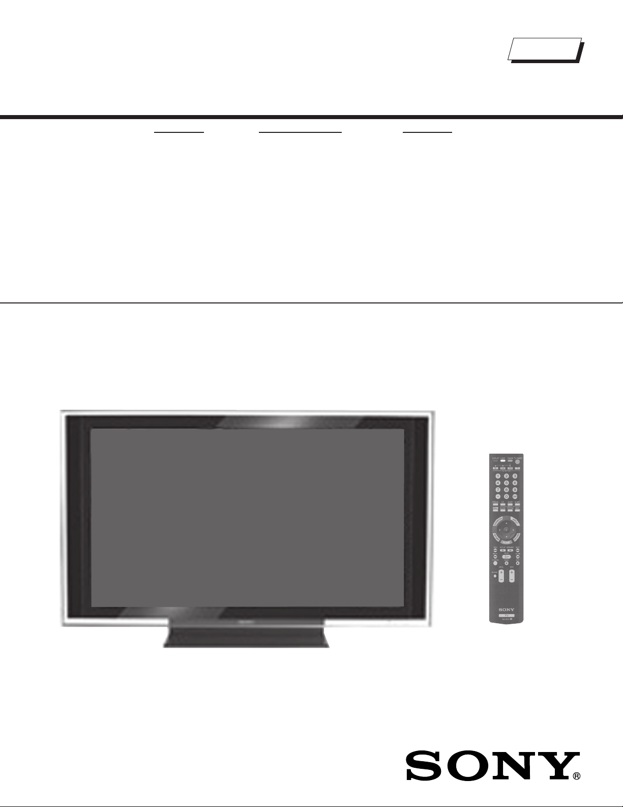
LCD DIGITAL COLOR TELEVISION
9-883-761-06
Self Diagnosis
Supported model
SERVICE MANUAL
MODEL NAME REMOTE COMMANDER DESTINATION
KDL-52XBR4
KDL-52XBR5
RM-YD017 US/CND
RM-YD017 US/CND
FIX2
CHASSIS
9-883-761-06
KDL-52XBR5 RM-YD017
LCD DIGITAL COLOR TELEVISION

KDL-52XBR4/52XBR5
TABLE OF CONTENTS
SECTION TITLE PAGE SECTION TITLE PAGE
Specifi cations ................................................................................. 4
Warnings and Cautions .................................................................. 6
Safety-Related Component Warning .............................................. 7
Safety Check-Out ........................................................................... 9
Self-Diagnostic Function ............................................................... 10
SECTION 1: DISASSEMBLY ............................................................... 12
1-1. Rear Cover Removal ............................................................ 12
1-2. Arm (Bracket) and Stand Removal ..................................... 12
1-3. Speaker Removal ................................................................ 13
1-4. HW2 Board Removal ........................................................... 13
1-5. H1 Board and H3 Board Removal ........................................ 14
1-6. UB1 Board Removal ............................................................ 14
1-7. FB1 Board, AU Board, and H5 Board
(For KDL-52XBR5 Only) Removal ....................................... 15
1-8. TUU2 Board Removal .......................................................... 15
1-9. GF2 Board, and DF4 Board and DF5 Board Removal ......... 16
1-10. H4 Board and AC Inlet Removal .......................................... 16
1-11. Stay Removal ....................................................................... 17
1-12. LCD Panel Removal ............................................................. 17
1-13. MT Inverter Board(s) Removal ............................................. 18
SECTION 2: SERVICE ADJUSTMENTS ............................................. 19
2-1. Remote Adjustment Buttons and Indicators ......................... 19
2-2. Accessing Service Adjustments ........................................... 19
2-3. Updating Model Information
after Replacing the FB1 Board ............................................. 21
SECTION 3: DIAGRAMS ..................................................................... 22
3-1. Circuit Boards Location ........................................................ 22
3-2. Printed Wiring Boards and
Schematic Diagrams Information ........................................ 22
3-3. Block Diagram ...................................................................... 24
3-3-1. Connector Diagram .................................................. 25
3-4. Schematics and Supporting Information .............................. 26
AU Board Schematic Diagram (1 of 6) ................................. 26
AU Board Schematic Diagram (2 of 6) ................................. 27
AU Board Schematic Diagram (3 of 6) ................................. 28
AU Board Schematic Diagram (4 of 6) ................................. 29
AU Board Schematic Diagram (5 of 6) ................................. 30
AU Board Schematic Diagram (6 of 6) ................................. 31
DF4 Board Schematic Diagram ........................................... 33
DF5 Board Schematic Diagram ........................................... 36
FB1 Board Schematic Diagram (1 of 17) ............................. 39
FB1 Board Schematic Diagram (2 of 17) ............................. 40
FB1 Board Schematic Diagram (3 of 17) ............................. 41
FB1 Board Schematic Diagram (4 of 17) ............................. 42
FB1 Board Schematic Diagram (5 of 17) ............................. 43
FB1 Board Schematic Diagram (6 of 17) ............................. 44
FB1 Board Schematic Diagram (7 of 17) ............................. 45
FB1 Board Schematic Diagram (8 of 17) ............................. 46
FB1 Board Schematic Diagram (9 of 17) ............................. 47
FB1 Board Schematic Diagram (10 of 17) ........................... 48
FB1 Board Schematic Diagram (11 of 17) ........................... 49
FB1 Board Schematic Diagram (12 of 17) ........................... 50
FB1 Board Schematic Diagram (13 of 17) ........................... 51
FB1 Board Schematic Diagram (14 of 17) ........................... 52
FB1 Board Schematic Diagram (15 of 17) ........................... 53
FB1 Board Schematic Diagram (16 of 17) ........................... 54
FB1 Board Schematic Diagram (17 of 17) ........................... 55
GF2 Board Schematic Diagram ........................................... 57
H1 Board Schematic Diagram .............................................. 59
H3 Board Schematic Diagram .............................................. 61
H4 Board Schematic Diagram .............................................. 63
H5 Board Schematic Diagram (KDL-52XBR5 ONLY) .......... 65
HW2 Board Schematic Diagram (1 of 2) .............................. 67
HW2 Board Schematic Diagram (2 of 2) .............................. 68
TUU2 Board Schematic Diagram (1 of 2) ............................ 71
TUU2 Board Schematic Diagram (2 of 2) ............................ 72
3-5. Semiconductors ................................................................... 75
SECTION 4: EXPLODED VIEWS ........................................................ 76
4-1. Rear Cover Assembly and Stand Assembly ........................ 76
4-2. Speakers .............................................................................. 77
4-3. Chassis ................................................................................ 78
4-4. Connectors ........................................................................... 79
4-5. Bezel Assembly and LCD Panel .......................................... 80
SECTION 5: ELECTRICAL PARTS LIST ............................................ 81
APPENDIX A: ENCRYPTION KEY COMPONENTS ..........................A-1
KDL-52XBR4/52XBR5
3

SPECIFICATIONS
y
KDL-52XBR4/52XBR5
Power Requirements
Power Consumption (W)
In Use (Max)
In Standby
120V-240V AC, 50/60Hz
320W
Less than 0.4W
VIDEO (IN) 1/2/3:
S Video (4-Pin Mini DIN (VIDEO 1 Only)
Y: 1.0 Vp-p, 75 ohms unbalanced, sync negative
C: 0.286 Vp-p (Burst signal), 75 ohms
Video
1.0 Vp-p, 75ohms unbalanced, sync negative
Audio
500 mVrms (100% modulation)
Impedance:47 kilohms
COMPONENT IN 1/2:
YP
Y:1.0 Vp-p, 75 ohms unbalanced, sync negative
PB:0.7 Vp-p, 75 ohms
PR:0.7 Vp-p, 75 ohms
Signal format: 480i, 480p, 720p, 1080i, 1080p
AUDIO
500 mVrms (100% modulation)
Impedance: 47 kilohms
(Component Video)
BPR
HDMI IN 1/2/3:
HDMI: Video:480i, 480p, 720p, 1080i,1080p, 1080/24p
Audio: Two channel linear PCM 32, 44.1 and
48 kHz, 16, 20 and 24 bits, Dolby Digital
AUDIO (for HDMI IN 1):
500 mVrms (100% modulation) (Fixed)
Impedance: 47 kilohms
AUDIO OUT:
500 mVrms (100% modulation) (Fixed)
1 Vrms at the maximum volume setting (Variable)
DIGITAL OUT (OPTICAL):
Optical Digital Audio Ouput (PCM/Dolby digital)
PC IN:
D-sub 15-pin, analog RGB, 0.7 Vp-p, 75 ohms, positive
PC AUDIO INPUT:
Stereo mini jack, 500 mVrms 1(100% modulation)
Impedance: 47 kilohoms
HEADPHONES:
Stereo mini jack
Impedance: 16 ohms
REMOTE:
RS232C, D-sub 9-pin (KDL-52XBR5 Only)
Trademark Information
Blu-ray Disc is a trademark.
“BRAVIA” and , BRAVIA ENGINE EX, “XMB”
and “XrossMediaBar”, S-Force, BRAVIA Theatre Sync, , DM
BRAVIA Internet Video Link Ready and “PS3” are trademarks
or registered marks of Sony Corporation and/or
Son
KDL-52XBR4/52XBR5
As an ENERGY STAR® Partner, Sony
Corporation has determined that this product
meets the ENERGY STAR
energy efficiency.
ENERGY STAR
®
is a U.S. registered mark.
Computer Entertainment Inc.
®
guidelines for
This TV is manufactured under license from Dolby
Laboratories. “Dolby” and the double-D symbol are
trademarks of Dolby Laboratories.
This TV incorporates HighDefinition Multimedia Interface
(HDMI
™
) technology. HDMI, the HDMI logo and High-
Definition Multimedia Interface are trademarks or
x
registered trademarks of HDMI Licensing LLC.
,
Design and specifi cations are subject to change without notice.
4
Speakers
Output
Full Range
Tweeter
Dimensions (W x H x D)
with stand
without stand
wall-mount hole pattern
Mass
with stand
without stand
KDL-52XBR4 KDL-52XBR5
11W + 11W
1/4
(4) 2 X 4
inches
(4) 50 X 105 mm
5/8
(2) 1
inches
(2) 40 mm
55
3/4
x 35
1/8
x 15
1/8
inches
1415 x 890 x 384 mm
3/4
5/8
55
x 32
7/8
x 4
inches 55
3/4
x 32
5/8
x 5 inches
1415 x 827 x 123 mm 1415 x 827 x 125 mm
400 x 300 mm
108 lbs.
49 kg
93 lbs.
42 kg
All measurements are approximations.
KDL-52XBR4/52XBR5
Television system
NTSC American TV Standard
ATSC (8VSB terrestrial) ATSC compliant 8VSB
QAM on cable ANSI/SCTE 07 2000
Channel coverage
Analog
2-69 Terrestrial
1-125 Cable
Digital
2-69 Terrestrial
1-135 Cable
Antenna
75-ohm external terminal for VHF/UHF
Panel System
LCD (Liquid Crystal Display) Panel
Display Resolution (horizontal x vertical):
1,920 dots x 1,080 lines
Screen Size (measured diagonally)
KDL-52XBR4/52XBR5 - ~52 inches
Supplied Accessories
Remote Commander RM-YD017
Two Size AA (R6) Batteries
75-ohm coaxial cable
AC Power Cord
HD15-HD15 Cable
Suport Belt (Lock Assy, Rudder) Securing Screw,
and Wood Screw
(See Bag Assy, Rudder Lock in the Accessories and Packing
section of the Electrical Parts List in this manual.)
Cable Holder (1 attached to the TV)
Operating Instructions
Quick Setup Guide
Warranty Card
Optional Accessories
Headphones Plug Adaptor
Connecting Cables
Wall-Mount Bracket
SU-WL500
KDL-52XBR4/52XBR5
5
KDL-52XBR4/52XBR5
WARNINGS AND CAUTIONS
CAUTION
These servicing instructions are for use by qualifi ed service personnel only. To reduce the risk of electric shock, do not perform any servicing other
than that contained in the operating instructions unless you are qualifi ed to do so.
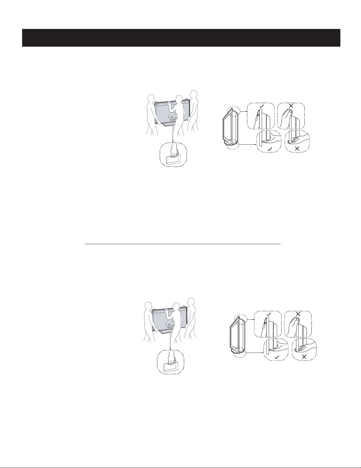
CARRYING THE TV
KDL-52XBR4/52XBR5
To avoid dropping the TV and causing serious injury,
be sure to follow these guidelines:
s Before carrying the TV, disconnect all cables.
s Carrying the large size TV requires two or more people.
s When you carry the TV, place your hand as
illustrated and hold it securely.
Do not put stress on the LCD panel.
s When lifting or moving the TV, hold it firmly from the bottom.
Place your palm directly under the panel.
s When carrying, do not subject the TV to shocks or vibration,
or excessive force.
WARNING!!
An isolation transformer should be used during any service to avoid possible shock hazard, because of live chassis. The chassis of this receiver is
directly connected to the ac power line.
! SAFETY-RELATED COMPONENT WARNING!!
Components identifi ed by shading and ! mark on the schematic diagrams, exploded views, and in the parts list are critical for safe operation. Replace
these components with Sony parts whose part numbers appear as shown in this manual or in supplements published by Sony. Circuit adjustments that
are critical for safe operation are identifi ed in this manual. Follow these procedures whenever critical components are replaced or improper operation is
suspected.
ATTENTION!!
Ces instructions de service sont à l’usage du personnel de service qualifi é seulement. Pour prévenir le risque de choc électrique, ne pas faire
l’entretien autre que celui contenu dans le Mode d’emploi à moins que vous soyez qualifi é faire ainsi.
POUR TRANSPORTER LE TÉLÉVISEUR
KDL-52XBR4/52XBR5
Assurez-vous de suivre ces consignes pour éviter de laisser
tomber le téléviseur et de provoquer des blessures graves :
s Avant de transporter le téléviseur,
débranchez tous les câbles.
s Le transport du téléviseur doit être
effectué par au moins deux personnes.
s Lorsque vous le transportez, placez vos
mains tel que cela est illustré et tenez solidement l’appareil.
N’appliquez pas de pression surl’écran ACL.
s Lorsque vous levez ou déplacez le téléviseur, assurez-vous de tenir
solidement de la base. Placez la paume des mains directement sous
le panneau.
s Lorsque vous transportez le téléviseur, ne le soumettez pas à des
chocs ou vibrations, ni à une force excessive.
Afi n d’eviter tout risque d’electrocution provenant d’un chássis sous tension, un transformateur d’isolement doit etre utilisé lors de tout dépannage. Le
chássis de ce récepteur est directement raccordé à l’alimentation du secteur.
! ATTENTION AUX COMPOSANTS RELATIFS A LA SECURITE!!
Les composants identifi es par une trame et par une marque ! sur les schemas de principe, les vues explosees et les listes de pieces sont d’une
importance critique pour la securite du fonctionnement. Ne les remplacer que par des composants Sony dont le numero de piece est indique dans le
present manuel ou dans des supplements publies par Sony. Les reglages de circuit dont l’importance est critique pour la securite du fonctionnement
sont identifi es dans le present manuel. Suivre ces procedures lors de chaque remplacement de composants critiques, ou lorsqu’un mauvais
fonctionnement suspecte.
KDL-52XBR4/52XBR5
6
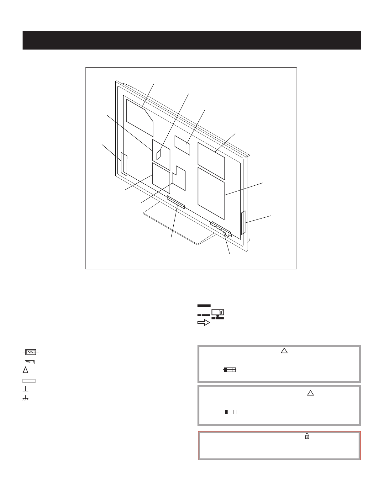
SAFETY-RELATED COMPONENT WARNING
KDL-52XBR4/52XBR5
There are critical components used in LCD color TVs that are important for safety. These components are identifi ed with shading and
mark on the schematic diagrams and the electrical parts list. It is essential that these critical parts be replaced only with the part number
specifi ed in the electrical parts list to prevent electric shock, fi re, or other hazard.
NOTE: Do not modify the original design without obtaining written permission from the manufacturer or you will void the original parts and
labor guarantee.
!
USE CAUTION WHEN HANDLING THE LCD PANEL
When repairing the LCD panel, be sure you are grounded by using a wrist band.
When installing the LCD panel on a wall, the LCD panel must be secured using the 4 mounting holes on the rear cover.
To avoid damaging the LCD panel:
do not press on the panel or frame edge to avoid the risk of electric shock.
do not scratch or press on the panel with any sharp objects.
do not leave the module in high temperatures or in areas of high humidity for an extended period of time.
do not expose the LCD panel to direct sunlight.
avoid contact with water. It may cause a short circuit within the module.
disconnect the AC adapter when replacing the backlight (CCFL) or inverter circuit.
(High voltage occurs at the inverter circuit at 650Vrms.)
always clean the LCD panel with a soft cloth material.
use care when handling the wires or connectors of the inverter circuit. Damaging the wires may cause a short.
protect the panel from ESD to avoid damaging the electronic circuit (C-MOS).
LEAKAGE CURRENT HOT CHECK CIRCUIT
KDL-52XBR4/52XBR5
7
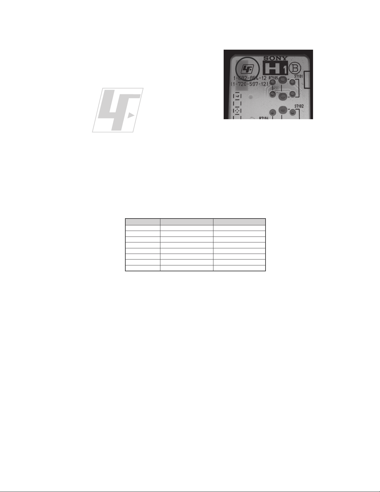
The circuit boards used in these models have been processed using
Lead Free Solder. The boards are identified by the LF logo located
close to the board designation e.g. H1 etc [ see example ]. The
servicing of these boards requires special precautions to be taken as
outlined below.
KDL-52XBR4/52XBR5
example 1
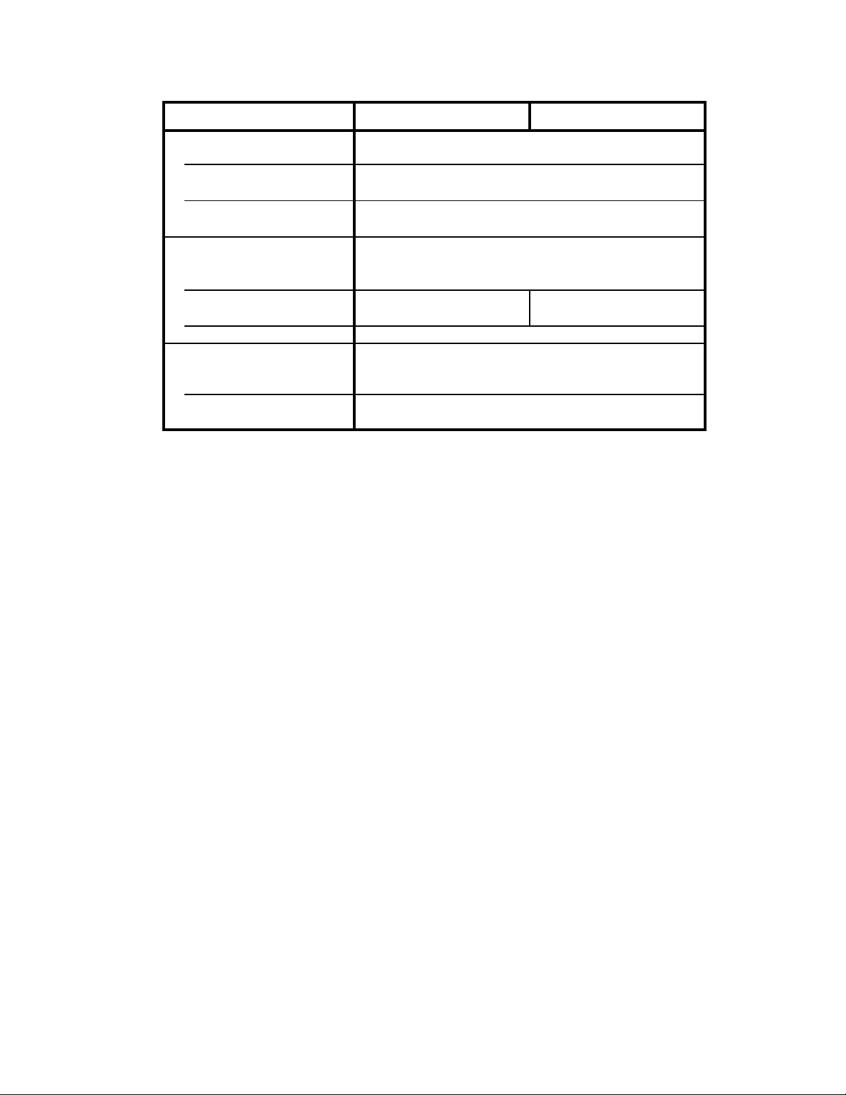
It is strongly recommended to use Lead Free Solder material in order to guarantee optimal quality of new solder joints.
Lead Free Solder is available under the following part numbers :
rebmuntraP retemaiD skrameR
91-500-046-7mm3.0gK52.0
02-500-046-7mm4.0gK05.0
12-500-046-7mm5.0gK05.0
22-500-046-7mm6.0gK52.0
32-500-046-7mm8.0gK00.1
42-500-046-7mm0.1gK00.1
52-500-046-7mm2.1gK00.1
62-500-046-7mm6.1gK00.1
Due to the higher melting point of Lead Free Solder the soldering iron tip temperature needs to be set to 370 degrees centigrade.
This requires soldering equipment capable of accurate temperature control coupled with a good heat recovery characteristics.
For more information on the use of Lead Free Solder, please refer to
http://www.sony-training.com
KDL-52XBR4/52XBR5
8
SAFETY CHECK-OUT
KDL-52XBR4/52XBR5
After correcting the original service problem, perform the following
safety checks before releasing the set to the customer:
1. Check the area of your repair for unsoldered or poorly soldered
connections. Check the entire board surface for solder splashes and
bridges.
2. Check the interboard wiring to ensure that no wires are “pinched” or
touching high-wattage resistors.
3. Check that all control knobs, shields, covers, ground straps, and
mounting hardware have been replaced. Be absolutely certain that
you have replaced all the insulators.
4. Look for unauthorized replacement parts, particularly transistors,
that were installed during a previous repair. Point them out to the
customer and recommend their replacement.
5. Look for parts which, though functioning, show obvious signs of
deterioration. Point them out to the customer and recommend their
replacement.
6. Check the line cords for cracks and abrasion. Recommend the
replacement of any such line cord to the customer.
7. Check the antenna terminals, metal trim, “metallized” knobs, screws,
and all other exposed metal parts for AC leakage. Check leakage as
described below.
The AC leakage from any exposed metal part to earth ground and
from all exposed metal parts to any exposed metal part having a
return to chassis, must not exceed 0.5 mA (500 microamperes).
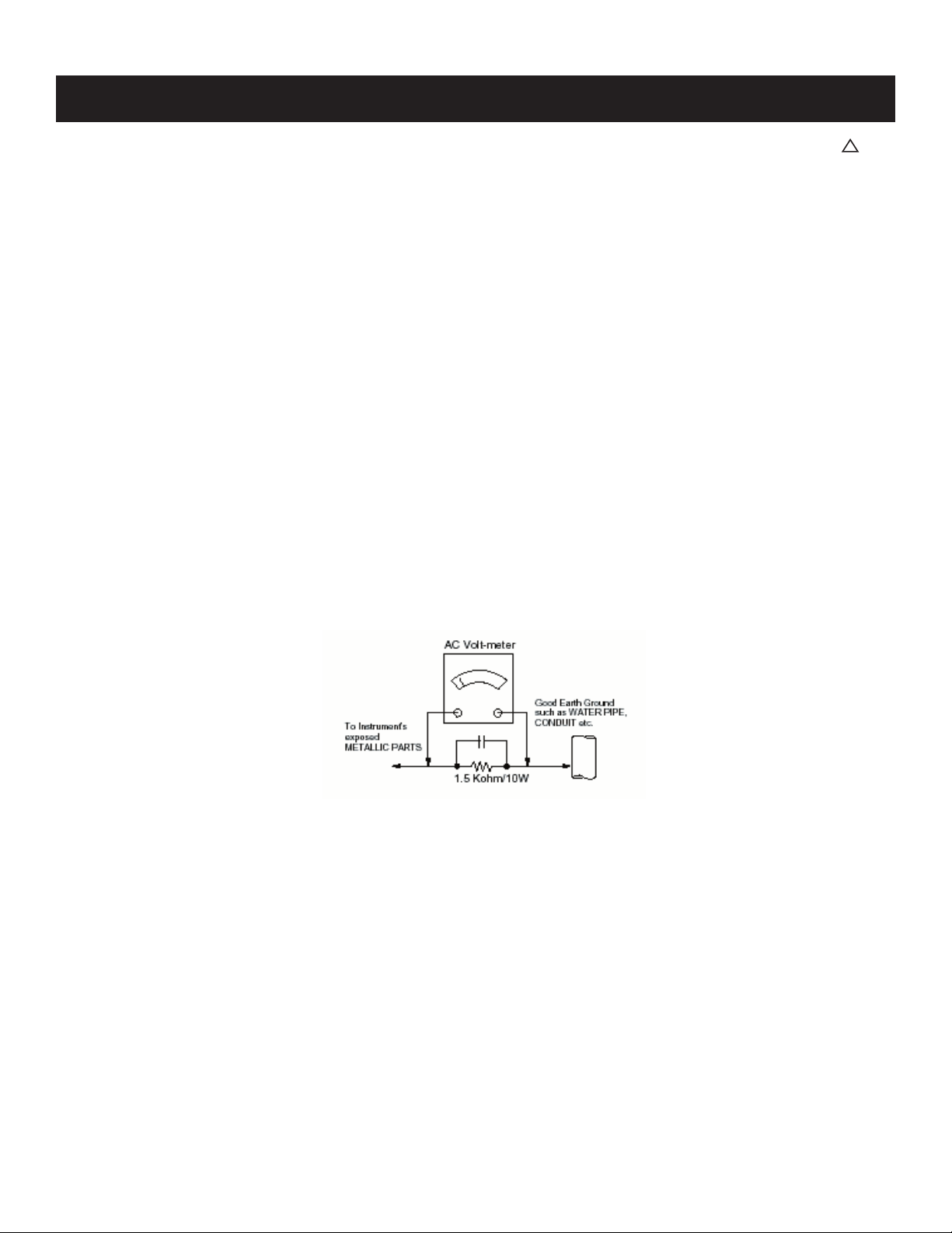
Leakage current can be measured by any one of three methods.
1. A commercial leakage tester, such as the Simpson 229 or RCA
WT-540A. Follow the manufacturers’ instructions to use these
instructions.
2. A battery-operated AC milliampmeter. The Data Precision 245
digital multimeter is suitable for this job.
3. Measuring the voltage drop across a resistor by means of a VOM
or battery-operated AC voltmeter. The “limit” indication is 0.75
V, so analog meters must have an accurate low voltage scale.
The Simpson’s 250 and Sanwa SH-63TRD are examples of
passive VOMs that are suitable. Nearly all battery-operated digital
multimeters that have a 2 VAC range are suitable (see Figure A).
How to Find a Good Earth Ground
A cold-water pipe is a guaranteed earth ground; the cover-plate
retaining screw on most AC outlet boxes is also at earth ground. If the
retaining screw is to be used as your earth ground, verify that it is at
ground by measuring the resistance between it and a cold-water pipe
with an ohmmeter. The reading should be zero ohms.
If a cold-water pipe is not accessible, connect a 60- to 100-watt
trouble- light (not a neon lamp) between the hot side of the receptacle
and the retaining screw. Try both slots, if necessary, to locate the hot
side on the line; the lamp should light at normal brilliance if the screw
is at ground potential (see Figure B).
Leakage Test
0.15 μF
Figure A. Using an AC voltmeter to check AC leakage. Figure B. Checking for earth ground.
To Exposed Metal
Parts on Set
Earth Ground
AC
Voltmeter
(0.75V)
Trouble Light
AC Outlet Box
Ohmmeter
Cold-water Pipe
KDL-52XBR4/52XBR5
9
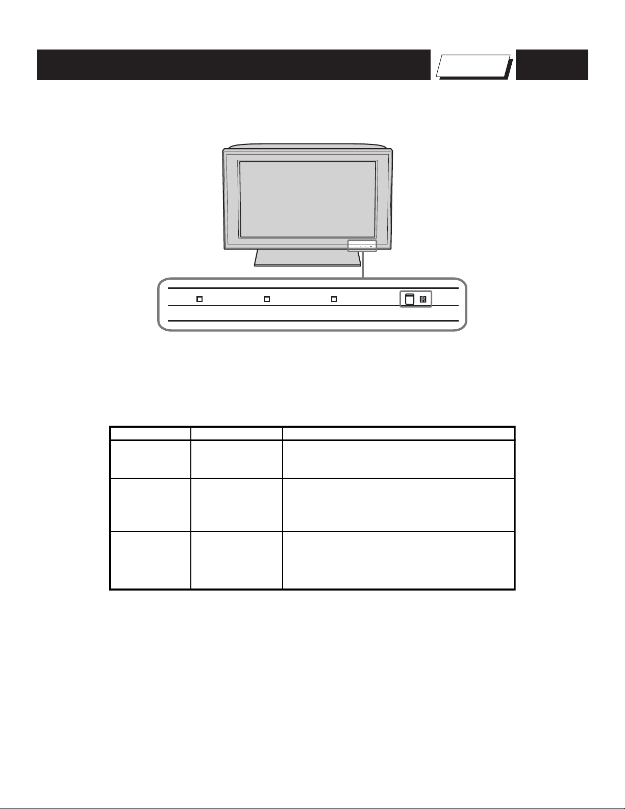
KDL-52XBR4/52XBR5
Control Buttons
SELF-DIAGNOSTIC FUNCTION
PIC OFF/TIMER STANDBY POWER
PIC OFF/TIMER STANDBY POWER
Self Diagnosis
Supported model
Description of LED Indictors
LED LED Type Description
POWER LED
STANDBY LED
PIC OFF/
TIMER
LED
Green LED
Red LED
Green or Orange
LED
* Light when the TV set is on
* Lights up in red when TV is in PC standby mode.
* If LED blinks continuously, this may indicate
that the TV needs servicing.
* Lights up in green when Picture Off is activated
* Lights up in orange when the timer is set
When timer is set, the LED remains lit even
when the TV is turned off.
KDL-52XBR4/52XBR5
10
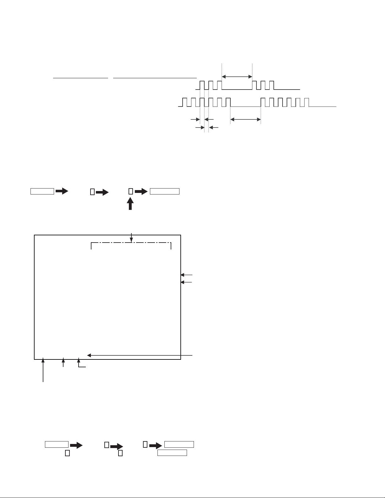
KDL-52XBR4/52XBR5
y
The units in this manual contain a self-diagnostic function. If an error occurs, the STANDBY LED automatically begins to fl ash. The number of times
the LED fl ashes translates to a probable source of the problem. A defi nition of the STANDBY LED fl ash indicators is listed in the instruction manual for
the user’s knowledge and reference. If an error symptom is diffi cult to reproduce use the Remote Commander to display the record that is stored at the
internal NVM to specify the cause.
- One flash is not used for self-diagnosis.
Example Diagnosis
Number of times LED Flash
LED OFF
3.0 sec
POW_ERR1 3 times
BACKLITE 6 times
LED ON : 0.3 sec
LED OFF : 0.3sec
Diagnostic Indicators
When an error occurs, the STANDBY LED fl ashes a set number of times to indicate the possible cause of the problem. If there is more than one error,
the LED will identify the fi rst of the problem areas. If the errors occur simultaneously, the one that corresponds to the fewest fl ashes is identifi ed fi rst.
(Results for all of the following diagnostic items are displayed on screen. No error has occurred if the screen displays a “00”)
1. TV must be in standby mode. (Power off).
2. Press the following buttons on the Remote Commander within a second of each other:
DISPLAY
The Self Check list displays.
This differs from accessing Service Adjustments.
☛
Channel 5 Volume -
Information Indicator displays time of last 3 events
alpsiDDEL
KCEHC FLES
: 000
PVO_WOP: 200
1RRE_WOP: 300
NOC_T: 500
ETILKCAB: 600
PMETLNAP: 700
TORP_DUA: 800
RRE_NAF: 900
RRE_TTD:010
:110
RECNALAB:310
TDW_TTD: 101
TDW_MVT: 201
TDW_MEB: 301
(Not used in FIX2 models)
TV POWER
------------ ------------ ------------ ====
------------ ------------ ------------
------------ ------------ ------------
------------ ------------ ------------
------------ ------------ ------------
------------ ------------ ------------
------------ ------------ ------------
------------ ------------ ------------
------------ ------------ ------------
------------ ------------ ------------ ====
------------ ------------ ------------
------------ ------------ ------------
------------ ------------ ------------
------------ ------------ ------------
.
00
00
00
00
LED OFF
3.0 sec
stnetnoC
====
PVO rewoP00
rorrE rewoP00
rorrE NOC-T00
rorrE thgilkcaBdetceted saw rorre on setacidni 000
rorrE pmeT lenaPdetceted saw rorre na setacidni 110
rotcetorP oiduA00
====
rorrE lenaP00
sremiT goD hctaW -TDW
sremiT goD hctaW(00
kcart ot desu era 00
,srossecorp orcim
).srorre drocer ot tonemit noitarepo dna tnuoc tooB0000-35000-97200
sledom eseht ni desU toN00
Boot count
(max 65535)
Operating Hours
(max 65535)
Resetting the Diagnostic Indicators
After completing the repair of the set, reset the Self Check screen to set all the display results to “00”.
1. TV must be in standby mode. (Power off).
2. Press
3. Press Channel 8, then press Channel 0. To exit press
DISPLAY
Panel Hours
(max 65535)
Channel 5 Volume -
TV POWER
TV POWER
.
.
KDL-52XBR4/52XBR5
11
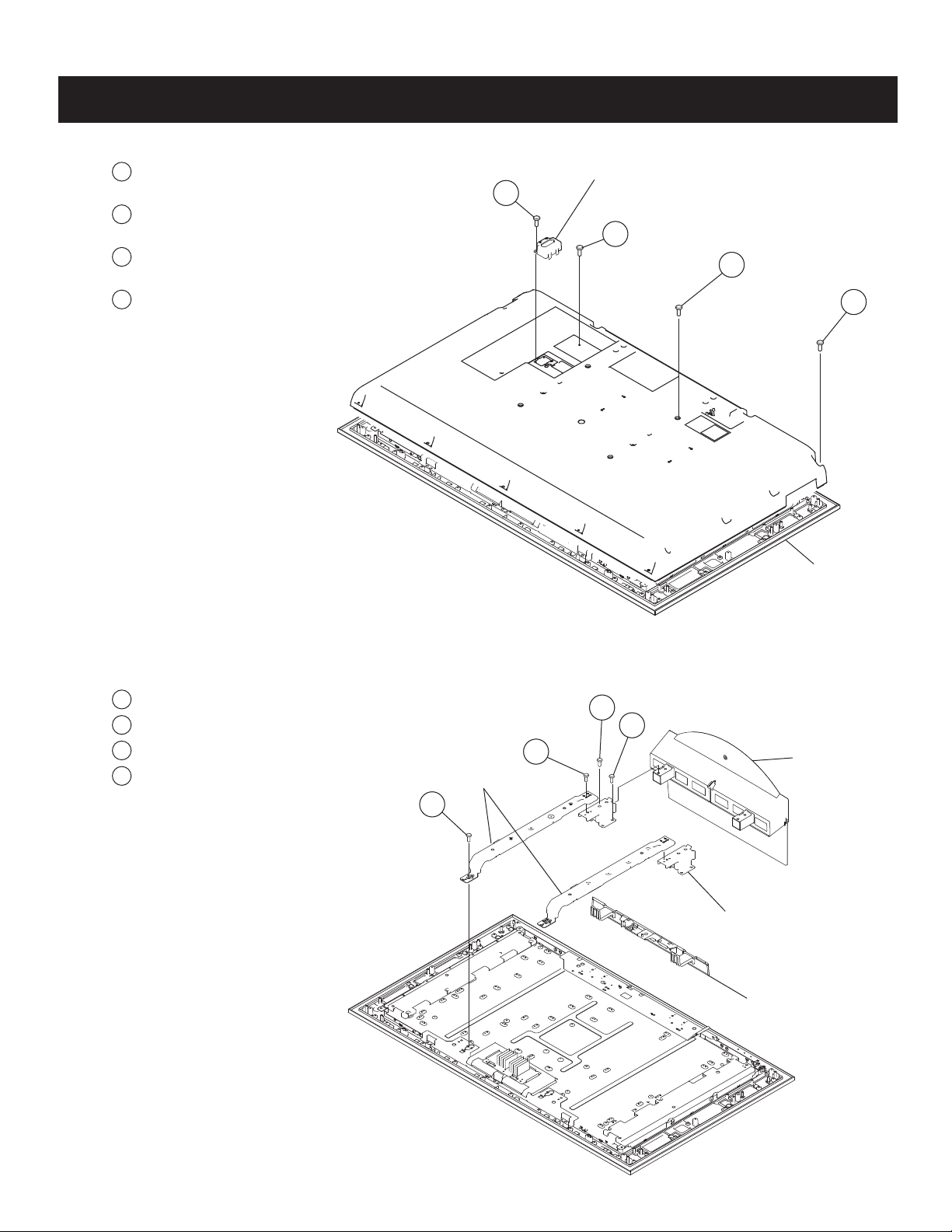
1-1. REAR COVER REMOVAL
1
Remove 2 screws from HOTEL Bracket
+BVTP 3X12 TYPE2 IT-3 (KDL-52XBR5 Only)
2
Remove 2 screws from Terminals,
+BVTP 3X12 TYPE2 IT-3
3
Remove 2 screws from Rear Cover arm positions,
+PSW M5X12
4
Remove 19 screws from Rear Cover, +BVTP2 4X16
KDL-52XBR4/52XBR5
SECTION 1: DISASSEMBLY
HOTEL Bracket (KDL-52XBR5 Only)
1
2
3
4
1-2. ARM (BRACKET) AND STAND REMOVAL
1
Remove 4 screws from top of Arms (Bracket), +PSW M5X8
2
Remove 4 screws from bottom of Arms (Bracket), +PSW M5X8
3
Remove 4 screws from Stand Holders and Stand, +PSW M5X12
4
Remove 4 screws, +BVST 4X8
Arms (Brackets)
1
Rear Cover
3
4
2
Arm Holder
Stand Assembly
Under Cover
KDL-52XBR4/52XBR5
12
1-3. SPEAKER REMOVAL
1
Remove 2 screws, +BWTP2 4X16
2
Remove 2 screws, +PSW M3X5
KDL-52XBR4/52XBR5
Loudspeaker (L)
1
2
Loudspeaker (R)
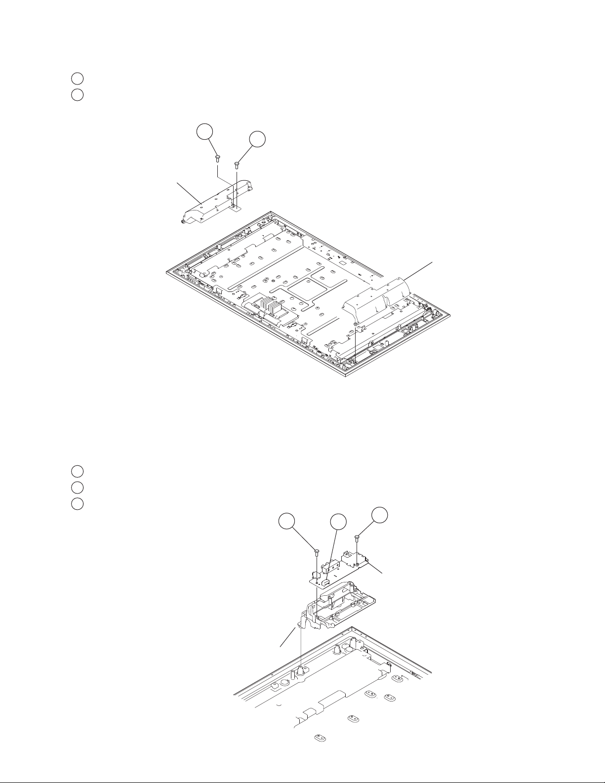
1-4. HW2 BOARD REMOVAL
1
Remove 2 screws, +BVTP 3X12 TYPE2 IT-3
2
Disconnect two connectors
3
Remove one screw, +PSW M3X5
Side Terminal Bracket
1
2
3
HW2 Board
KDL-52XBR4/52XBR5
13
1-5. H1 BOARD AND H3 BOARD REMOVAL
1
Disconnect one connector.
2
Release hooks and remove H3 Board.
3
Remove one screw, +BVTP2 4X16
4
Disconnect one connector.
5
Release hooks and remove H1 Board.
KDL-52XBR4/52XBR5
H3 Board
1-6. UB1 BOARD REMOVAL
1
Remove 4 screws, +PSW 3X8
2
Remove one screw, +PSW 3X8
3
Disconnect 2 connectors.
1
3
2
4
H1 Board
5
Multi Button
Control Bracket
KDL-52XBR4/52XBR5
1
2
UB1 Shield
3
UB1 Board
14
KDL-52XBR4/52XBR5
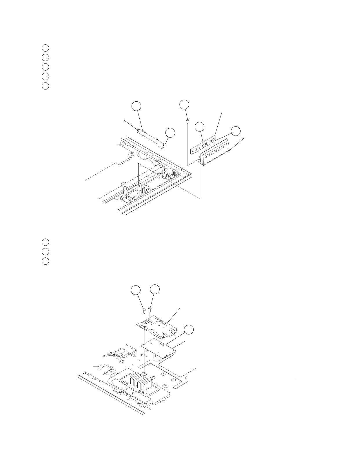
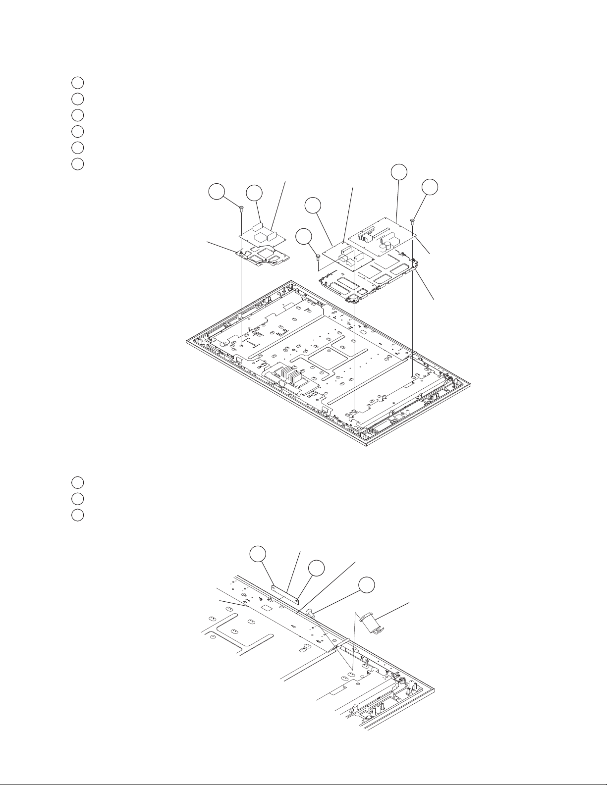
1-7. FB1 BOARD, AU BOARD, AND H5 BOARD (FOR KDL-52XBR5 ONLY) REMOVAL
1
Slide out Card Bracket
2
Remove 2 screws, +PSW M3X5
3
Remove 2 screws, HEX
4
Remove 4 screws, +BVST 3X8
5
Remove 7 screws, +BVST 3X8
6
Disconnect 7 connectors
7
Remove H5 Board
(For KDL-52XBR5 Only)
8
Disconnect 8 connectors
9
Remove 9 screws, +BVST 3X8
10
Remove 8 screws, +PSW M3X5
Card Bracket
1
4
5
10
FB Shield (Top)
3
2
H5 Board (KDL-52XBR5 Only)
7
6
FB1 Board
8
AU Board
Chassis Bracket
9
1-8. TUU2 BOARD REMOVAL
1
Remove 2 screws, +BVST 3X8
2
Remove one Hex. Nut from Tuner
3
Remove Tuner Bracket
4
Disconnect one connector
5
Remove 5 screws, +BVST 3X8
6
Remove 4 screws, +BVST 3X8
7
Remove one screw, +BVST 4X8
1
5
TUU Shield (Top)
4
2
3
Tuner Bracket
TUU2 Board
TUU Shield (Bottom)
6
7
Chassis Bracket
KDL-52XBR4/52XBR5
15
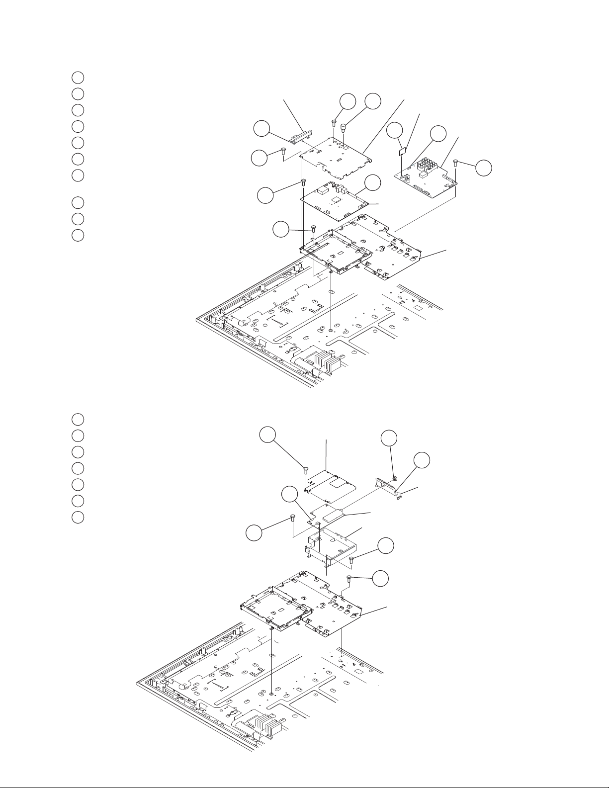
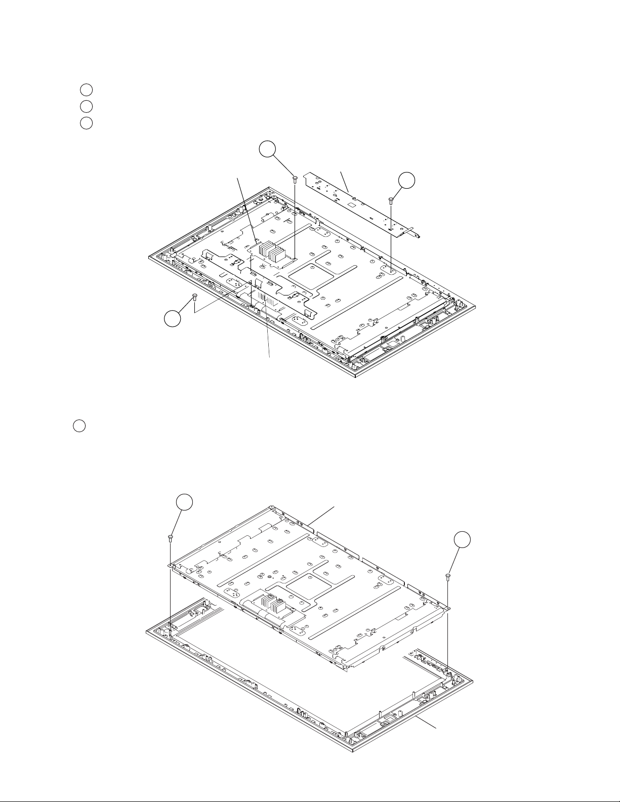
1-9. GF2 BOARD, AND DF4 BOARD AND DF5 BOARD REMOVAL
1
Remove 5 screws, +PSW 3SG
2
Disconnect 3 connectors
3
Disconnect 5 connectors
4
Remove 4 screws, +PSW 3SG
5
Disconnect 8 connectors
6
Remove 4 screws, +PSW 3SG
DF5 Board
1
2
DF4 Board
3
5
KDL-52XBR4/52XBR5
6
DF5 Bracket
1-10. H4 BOARD AND AC INLET REMOVAL
1
Disconnect one connector.
2
Release hooks and remove H4 Board.
3
Remove 2 screws, +KTT 3X10 (S type)
4
GF2 Board
G/D Bracket
KDL-52XBR4/52XBR5
Lower Stay
1
H4 Board
2
Front Cabinet Assembly
3
AC Inlet
16
1-11. STAY REMOVAL
1
Remove 3 Screws, +BVTP2 4X16
2
Remove 2 Screws, +PSW M3X5
3
Remove 4 screws, +PSW M5X8
KDL-52XBR4/52XBR5
2
Fin Bracket
1
Lower Stay
3
1-12. LCD PANEL REMOVAL
1
Remove 4 screws, +BSW M5X12
1
Upper Stay
LCD Panel
1
KDL-52XBR4/52XBR5
Front Cabinet
17
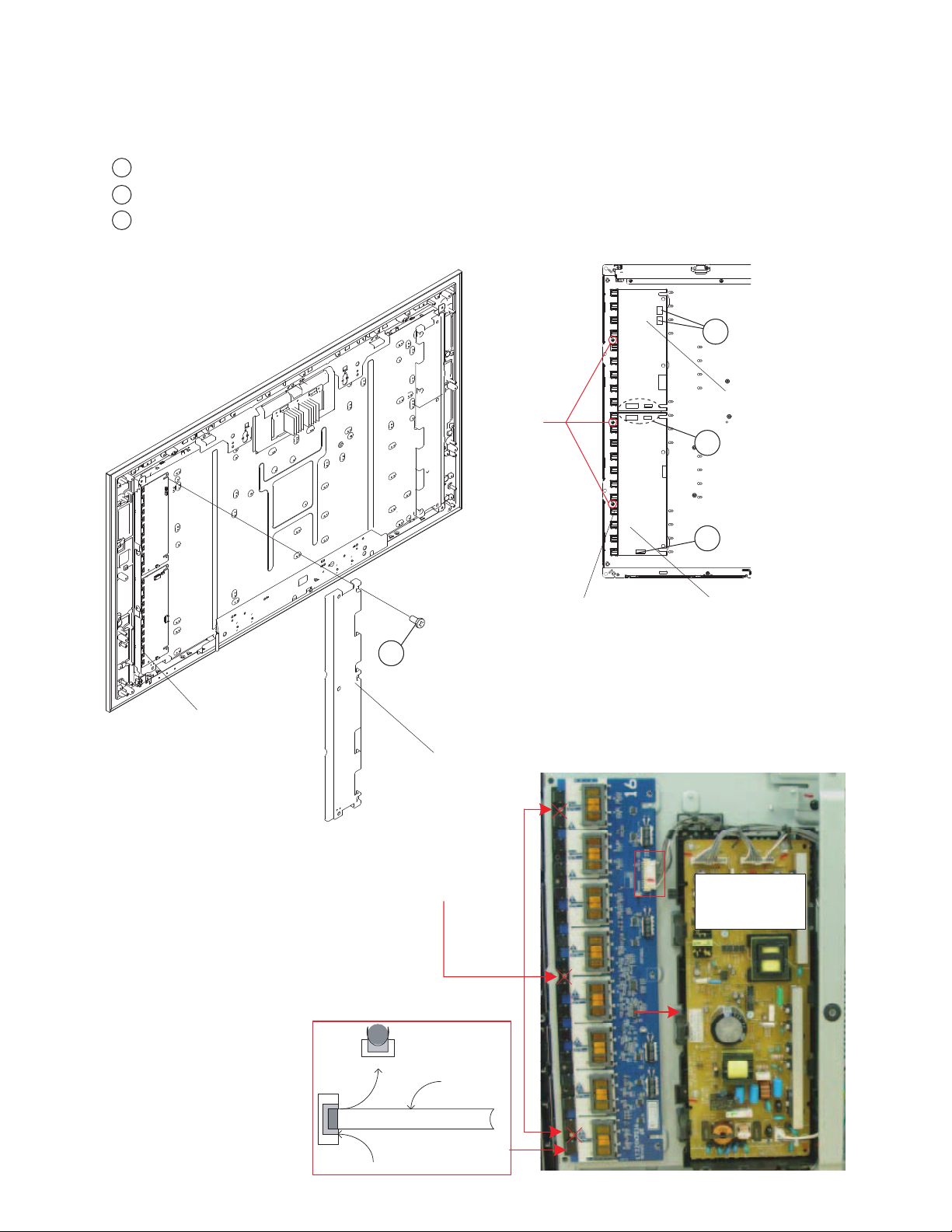
1-13. MT INVERTER BOARD(S) REMOVAL
CAUTION:
Be sure to identify the inverter cover screws before proceeding. DO NOT remove the screws securing the plastic strip holding the lamp
sockets.
1
Remove screws securing the inverter cover.
2
Disconnect the 2 connectors from the board you are removing that connects the upper inverter board to the lower inverter board.
3
To remove the lower board, disconnect 1 connector.
To remove the upper board, disconnect 2 connectors.
KDL-52XBR4/52XBR5
3
Plastic Strip
holding
Lamp Socket
INVERTER BOARD REMOVAL
Only remove the screws securing the inverter
cover which may be metal or plastic. The
remaining plastic strip contains sockets for the
fluorescent backlights and should never be
loosened. The backlights will pop out of the
sockets and/or break the backlight requiring a
LCD panel replacement. The example shown
is a 32” model but applies to all models.
DO NOT
REMOVE
BACKLIGHT
SCREWS
1
NOTE: The connector that attaches the Left Upper Inverter board
to the DF5 board has a strip of white tape at both ends of the connector.
The connector that attaches the Right Upper Inverter board
to the DF4 board has a strip of red tape at both ends of the connector.
Inverter Cover
WARNING
NEVER REMOVE THE
SCREWS SECURING THE
PLASTIC STRIP HOLDING
THE LAMP SOCKETS
DAMAGE TO THE
BACKLIGHT TUBES WILL
OCCUR!
!
.
Plastic Strip
holding
Lamp Socket
Left Upper Inverter Board
2
3
Left Lower Inverter Board
REMOVE
CONNECTOR AND
PULL BOARD TO
THE RIGHT
KDL-52XBR4/52XBR5
END VIEW
BACKLIGHT
SOCKET
18
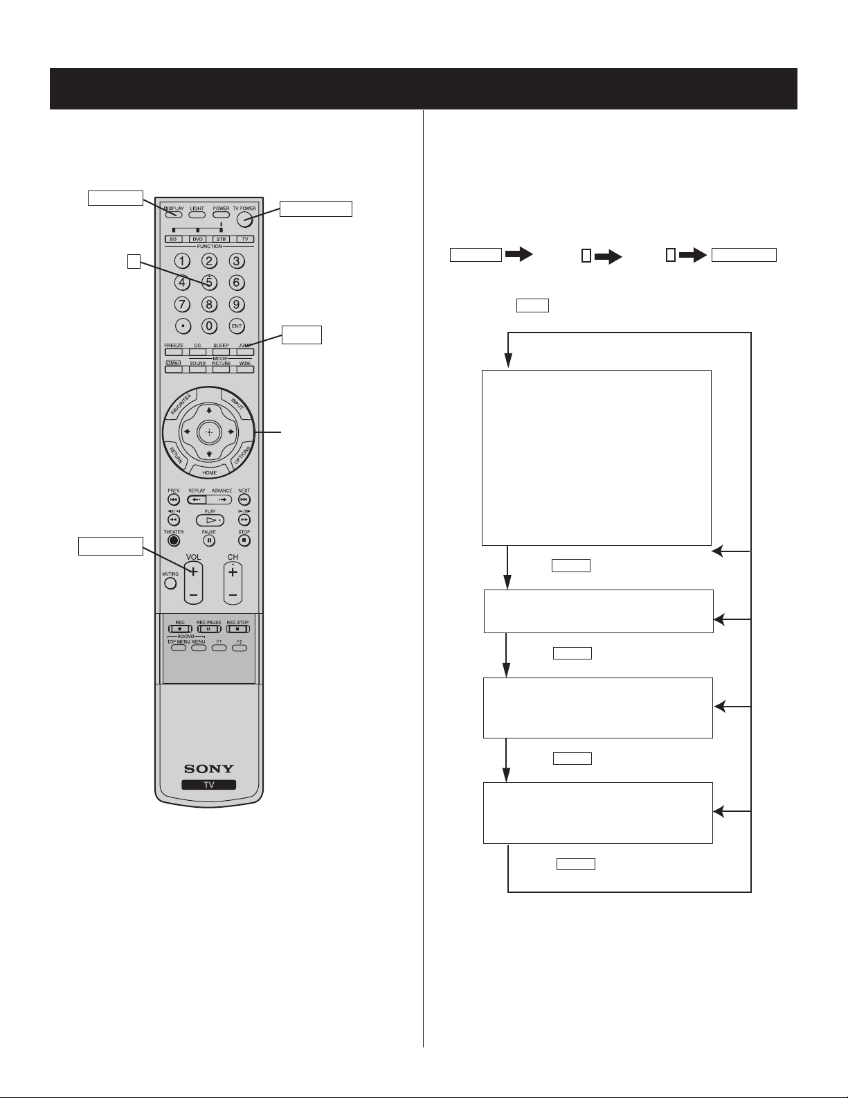
SECTION 2: SERVICE ADJUSTMENTS
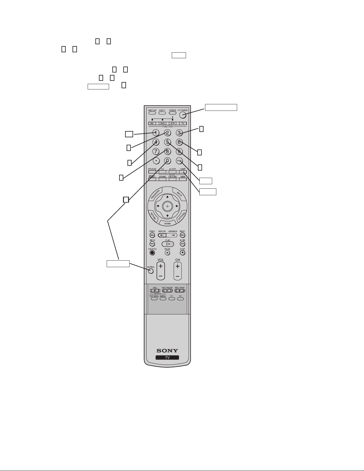
KDL-52XBR4/52XBR5
2-1. REMOTE ADJUSTMENT BUTTONS AND
INDICATORS
DISPLAY
5
VOLUME+
TV POWER
JUMP
Onscreen cursor
and select button
2-2. ACCESSING SERVICE ADJUSTMENTS
To adjust various set features, use the Remote Commander to put the set
into service mode to display the service menus.
1. TV must be in standby mode. (Power off).
2. Press the following buttons on the Remote Commander within a
second of each other:
DISPLAY
The fi rst service menu (TV) displays.
3. To display the service menu that contains the category you want to
adjust, press
Channel 5 Volume +
JUMP
on the Remote Commander.
DIGITAL
001 OP
M2.001C
Press JUMP
000 000 VERS
<SUB><DIGITAL>
SMO.100W00AADM0. 159A00AA
SD0.010W00AADD0.000A00LU
SB1.000W00AA
<BE>
BM0.050W00AU
BD0.049A00LUW
BB0.029W00AU
SERVICE
TV POWER
.
CHASSIS SERVICE
000 GR
000 GRMD 0
Press JUMP
SUB SERVICE
000 VERS
000 MODEL
MODEL ID: XXXXXXXXXX
Press JUMP
BEM SERVICE
BOOT: 0. 026W00AU
RM-YD017
MAIN: 0. 050W00AU
DATA: 0. 049A00LUW
Press JUMP
KDL-52XBR4/52XBR5
19
The screen displays the fi rst category in the selected service menu.
4. To change the category, press
Note: Pressing 2 or 5 only changes the categories within the service menu displayed.
To change a category on one of the other service menus, press the
correct service menu is displayed.
5. To change the adjustment item, press 1 or 4 on the Remote Commander.
6. To change the data value, press 3 or 6 on the Remote Commander.
7. To write into memory, press
8. To exit service mode, turn the power off.
2
or 5 on the Remote Commander.
MUTING
then 0 on the Remote Commander.
JUMP
button until the
TV POWER
Increase
Next item
1
3
Data value
KDL-52XBR4/52XBR5
Next
Category
Previous
item
Restore User Control
and Channel Memory
Write to
memory
2
4
8
0
MUTING
Decrease
6
Data value
Previous
5
Category
ENT
JUMP
Displays Service Menus
KDL-52XBR4/52XBR5
RM-YD017
20
2-3. UPDATING MODEL INFORMATION
AFTER REPLACING THE FB1 BOARD
Complete the following steps to reset the model information to the
correct size after replacing the FB1 Board.
1. Access the Service Menu by pressing the following buttons on the
Remote Commander within a second:
DISPLAY
The service menu displays.
2. Press the
3. Press 2 until the 0001 MODEL_INFO category displays.
Channel 5 Volume +
JUMP
button until the BEM micro service menu displays.
BEM SERVICE
BOOT: 0. 026W00AU
MAIN: 0. 050W00AU
DATA: 0. 049A00LUW
BEM SERVICE
0001 MODEL_INFO
0001 PANEL_SIZE 0
DIFF 1
TV POWER
Update
according to
panel size
.
KDL-52XBR4/52XBR5
4. Press 3 to increase the value to 2.
5. To write to memory, press
MUTING
then 0 on the Remote
Commander.
8. To exit service mode, turn the power off.
KDL-52XBR4/52XBR5
21
3-1. CIRCUIT BOARDS LOCATION
FB1
HW2
AU
TUU2
KDL-52XBR4/52XBR5
SECTION 3: DIAGRAMS
DF5
H5
(KDL-52XBR5 ONLY)
UB1
DF4
GF2
H1
H4
3-2. PRINTED WIRING BOARDS
AND SCHEMATIC DIAGRAMS INFORMATION
All capacitors are in μF unless otherwise noted. pF : μμF 50WV or
less are not indicated except for electrolytics and tantalums.
All electrolytics are in 50V unless otherwise specifi ed.
All resistors are in ohms. kΩ=1000Ω, MΩ=1000kΩ
Indication of resistance, which does not have one for rating
electrical power, is as follows: Pitch : 5mm
Rating electrical power :
1
/
W in resistance, 1/
4
W and 1/
10
W in chip resistance.
16
1
/
W
4
: nonfl ammable resistor
: fusible resistor
: internal component
: panel designation and adjustment for repair
: earth ground
: earth-chassis
All variable and adjustable resistors have characteristic curve B,
unless otherwise noted.
Readings are taken with a color-bar signal input.
Readings are taken with a 10MΩ digital multimeter.
Voltages are DC with respect to ground unless otherwise noted.
Voltage variations may be noted due to normal production
tolerances.
H3
All voltages are in V.
S : Measurement impossibility.
: B+line.
: B-line. (Actual measured value may be different).
: signal path. (RF)
Circled numbers are waveform references.
The components identifi ed by shading and ! symbol are critical for safety. Replace
only with part number specifi ed.
The symbol indicates a fast operating fuse and is displayed on the component
side of the board. Replace only with fuse of the same rating as marked.
!
Les composants identifi es per un trame et une marque
securite. Ne les remplacer que par une piece portant le numero specifi e.
Le symbole indique une fusible a action rapide. Doit etre remplace par une
fusible de meme yaleur, comme maque.
NOTE: The components identifi ed by a red outline and a mark contain confi dential
information. Specifi c instructions must be adhered to whenever these components
are repaired and/or replaced.
See Appendix A: Encryption Key Components in the back of this manual.
sont critiques pour la
KDL-52XBR4/52XBR5
22
KDL-52XBR4/52XBR5
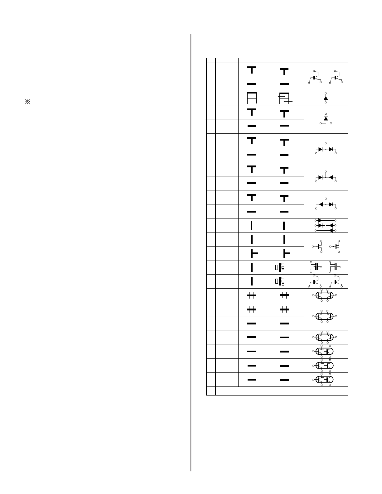
REFERENCE INFORMATION
RESISTOR
: RN METAL FILM
: RC SOLID
: FPRD NONFLAMMABLE CARBON
: FUSE NONFLAMMABLE FUSIBLE
: RW NONFLAMMABLE WIREWOUND
: RS NONFLAMMABLE METAL OXIDE
: RB NONFLAMMABLE CEMENT
: ADJUSTMENT RESISTOR
COIL
: LF-8L MICRO INDUCTOR
CAPACITOR
: TA TANTALUM
: PS STYROL
: PP POLYPROPYLENE
: PT MYLAR
: MPS METALIZED POLYESTER
: MPP METALIZED POLYPROPYLENE
: ALB BIPOLAR
: ALT HIGH TEMPERATURE
: ALR HIGH RIPPLE
Terminal name of semiconductors in silk screen
printed circuit ( )
Device Printed symbol Terminal name
Transistor
1
Transistor
2
3
Diode
4
Diode
Diode
5
Diode
6
Diode
7
8
Diode
Diode
9
Diode
0
Diode
!¡
Diode
!™
Transistor
!£
(FET)
Transistor
!¢
(FET)
Transistor
!?
(FET)
Transistor
!§
Transistor
!¶
Transistor
!•
Transistor
!ª
Transistor
@º
Transistor
@¡
Transistor
@™
Transistor
@£
Discrete semiconductot
–
(Chip semiconductors that are not actually used are included.)
*
Collector
Base
Collector
Base
Cathode
Cathode
Anode
Cathode
Anode
Common
Anode
Common
Anode Cathode
Common
Anode
Common
Anode Anode
Common
Cathode
Common
Cathode
Anode
Anode
Cathode
Drain
Drain
B1 E1
C2
B2 C1E2
B2 E2
C1
B1 C2
E1
B2 E2
C1
B1 C2E1
B2 E2
C1
B1 C2E1
E2
B1 E1
C2
(B2)
E1
B1
C1
(B2)
E1
E2
C2
Emitter
Emitter
Anode
(NC)
(NC)
Cathode
Anode
Cathode
Cathode
Cathode
Anode
Anode
Source
Gate
Source
Gate
Source
Drain
Gate
Emitter
Collector
Base
C1(B2)
E2
C2
B1
C1
Circuit
D
G
D
S
B1
B1
B1
B1
B1
B1
D
G
S
S
D
G
C1
E1
C1
E1
E1
C1
E2
C1
C1
G
S
C2
B2
E2
C2
B2
E2
E2
B2
C2
C2C1(B2)
E2
E2E1(B2)
C2
C2E1(B2)
C2
Ver.1.6
KDL-52XBR4/52XBR5
23
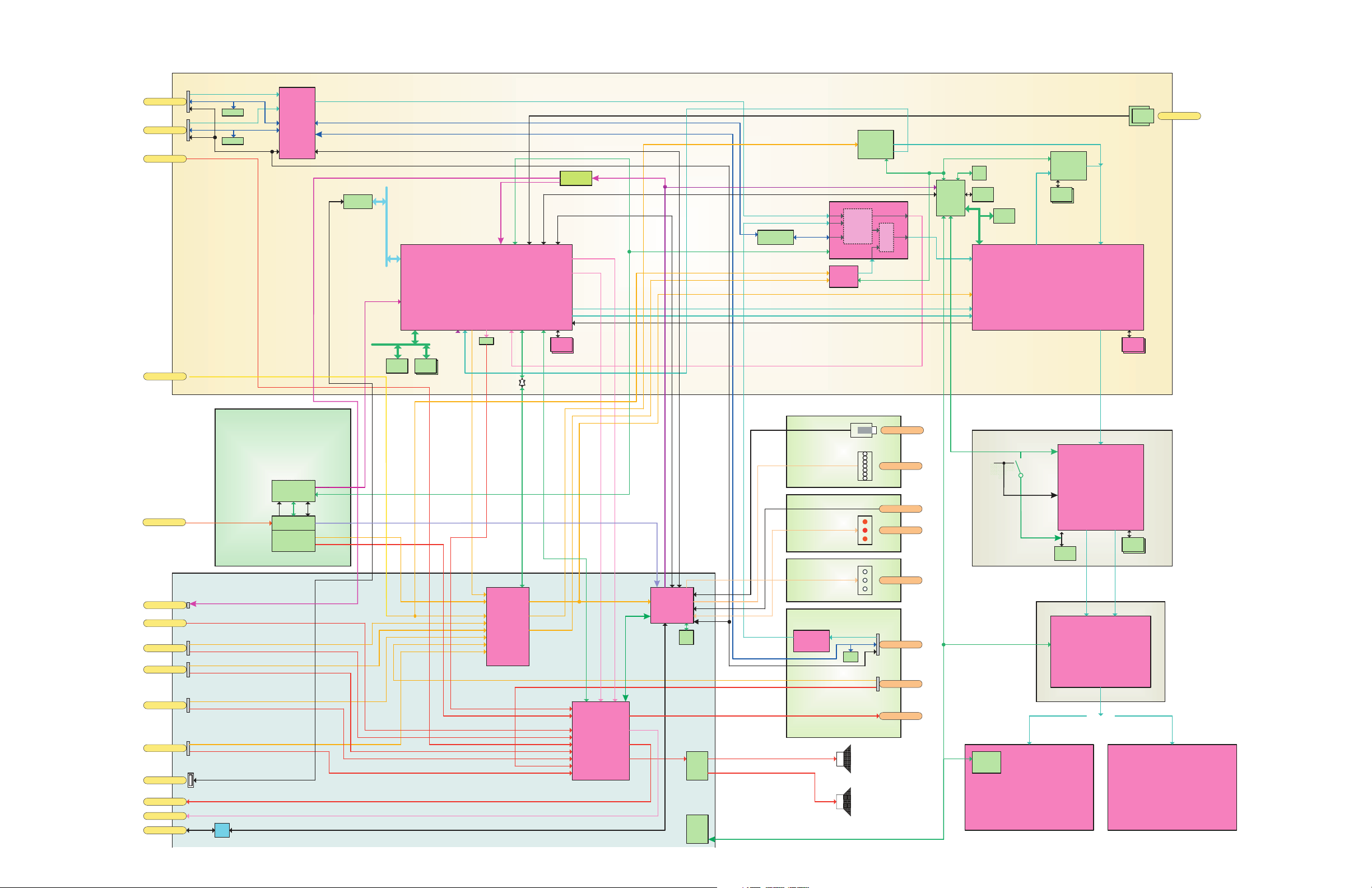
3-3. BLOCK DIAGRAM
FB1
HDM I I N 1
HDM I I N 3
Audio IN
TMDS1
DDC1
CEC
TMDS3
DDC3
CEC
Audio L/ R
NVM2KB
EDID
NVM2KB
EDID
HDMI
Equalizer
CXB1444
TMDS
DDC
USB2.0
(HS)
uPD720101
KDL-52XBR4/52XBR5
MS D/L
Sub Chroma
CCP- XA
DRC
I2C
MFV2.5
SDRAM
SDRAM
64Mb x2
64Mb x2
EPP
BE Micro
I2C
I2C
I2C
EEP
SDRAM
64Mb
Flash
I2C
Bus
SW
I2C
I2S
SW(Buffer)
UART
PCI
I2C
UART
SN74LV4053
SPD IF
I2S(5.1ch)
SPI(D L)
HDMIRx
Sel.
DDC
X2
I2C
V1.3
10bitA DC
EMMA2TH
TS
Main
Gfx
H/ V
MS Service
D-
Sub1 5
RF- 1
Modem
AudioMini
Componennt1
Componennt2
SVide o1
AU
Analog RGB H/V
TUU
Audio L/ R
Analog Y/Cb/ Cr
Audio L/ R
Analog Y/Cb/ Cr
Audio L/ R
Analog CVBS Y/C
Audio L/ R
Demodulator
8VSB/64QAM
256QAM/QPSK
I2C GPIOFA T
Tuner(Main)
Demodulator
NTSC/ BTSC
I2C
H_SYNC
Analog CVBS
Audio L/ R
Local Bus
USB
NOR
2Mbit
NAND
NAND
64MB x2
32MB x2
DA
Video
SW1
CXA2239
14 Input
5Output
3-5
I2C I2C
I2C
CVBS/YC
CVBS/YC/ YCbCr
YCbCr/ RGB
DDR2
DDR2
SDRAM
SDRAM
512Mbit x2
512Mbit x 2
DDR2
DDR2
SDRAM
SDRAM
256Mbit x2
256Mbit x2
H1
KEYcontrol
SPI
(DL)
H3
LED control
H4
Sub Micro
Rigel
I2C
I2C
EEP
I2C
HW2
HDMI
Equalizer
CXB1443
NVM
2KB
EDID
Analog CVBS
Audio L/ R
TMDS2
DDC2
CEC
Power Sw.
KEY
SIRCS
LED
SONY Logo
HDMI IN2
Video2
HP OUT
UB1(HFR)
Cayenne_bint
I2C
FRC2007
DDR
DDR
SDRAM
SSDRARAM
128Mbit x2
DDR
NVM
128Mbibittxx22
M
128M
T- Con
I2C
T-Con
KDL-52XBR4/52XBR5
Video3
USB
L/R OUT
Opt. OUT
RS232C
Analog CVBS
Audio L/ R
Audio L/ R
SPD IF
Buff
UART
Audio DSP
TAS 3208
Power
AM
TEMP
Sensor
I2C
P
Full HD
LB
Micro
HFR
S-PVA
LED BackLight
70"
LCD-Panel
Full HD
HFR
S-PVA
WCG CCFL BackLight
40",46" ,52"
LCD-Panel
24
3-3-1. CONNECTOR DIAGRAM
㪀
㪚㪥㪎㪇㪉㪉
㪛㪝㪋
㪞㪝㪉
㪬㪙㪈
㪫㪬㪬㪉
㪟㪋
㪟㪮㪉
㪝㪙㪈
㩷㪝㪠㪯㪉㪄㪯㪌㪉
㪛㪝㪌
㪘㪬
㪟㪊
㪟㪈
㪪㪧
㪙㪦㪯
㪪㪧
㪙㪦㪯
䇭䊋䊤䊮䉰㪄ၮ᧼䇭㪙㪸㫃㪸㫅㪺㪼㫉㩷㪙㫆㪸㫉㪻
䇭㪙㪸㫃㪸㫅㪺㪼㫉㩷㪙㫆㪸㫉㪻
KDL-52XBR4/52XBR5
㪚㪥㪍㪎㪇㪎㩿㪋㫇
㪚㪥㪍㪎㪇㪏㩿㪊㫇㪀 㪣㪭㪛㪪㪄㪌㪈㪧
㪚㪥㪍㪍㪇㪇 㪚㪥㪍㪎㪇㪍
㪚㪥㪍㪌㪇㪉 㪚㪥㪍㪈㪌㪊 㪚㪥㪈㪇㪇㪊 㪚㪥㪈㪍㪇㪉
㩷㩷㩷㩷㪚㪥㪍㪌㪇㪈
㩷㩷㪚㪥㪍㪌㪇㪊 㪚㪥㪍㪌㪇㪌
㩷㩷㩷㪚㪥㪍㪋㪇㪇 㪚㪥㪍㪌㪇㪋
㪚㪥㪌㪍㪇㪈 㪚㪥㪋㪊㪇㪉
㩷㩷㩷㩷㪚㪥㪍㪎㪇㪈 㪣㪭㪛㪪㪄㪌㪈㪧
㪚㪥㪎㪉㪇㪇
㩷
㪚㪥㪍㪎㪇㪋
㩷㩷㩷㩷㪚㪥㪎㪉㪇㪈 㪚㪥㪌㪍㪇㪇
㩷
㪚㪥㪉㪐㪇㪇
㩷㩷㩷㪚㪥㪉㪎㪇㪈
㪝㪝㪚㪄㪋㪐㫇
㪚㪥㪍㪌㪇㪈
㪚㪥㪍㪈㪌㪈
㪚㪥㪍㪈㪌㪇
㩷
㪚㪥㪇㪇㪈
㩷㩷㩷㩷㪚㪥㪏㪇㪈
㪚㪥㪊㪇㪇㪈
㩷㩷㩷㩷㩷㩷㩷
㩷㩷
㪚㪥㪍㪈㪌㪋
㩷
㪚㪥㪊㪉㪇㪈
㪚㪥㪊㪊㪇㪈
㪚㪥㪇㪇㪉 㩷㩷㩷㪚㪥㪇㪇㪋 㩷㩷㪣㪭㪛㪪㪄㪉㪈㫇
㩷㩷㩷㩷㪚㪥㪎㪇㪍㪈
㩷
㩷
㩷㩷㩷㩷㩷㩷㩷
㩷㪚
KDL-52XBR4/52XBR5
25
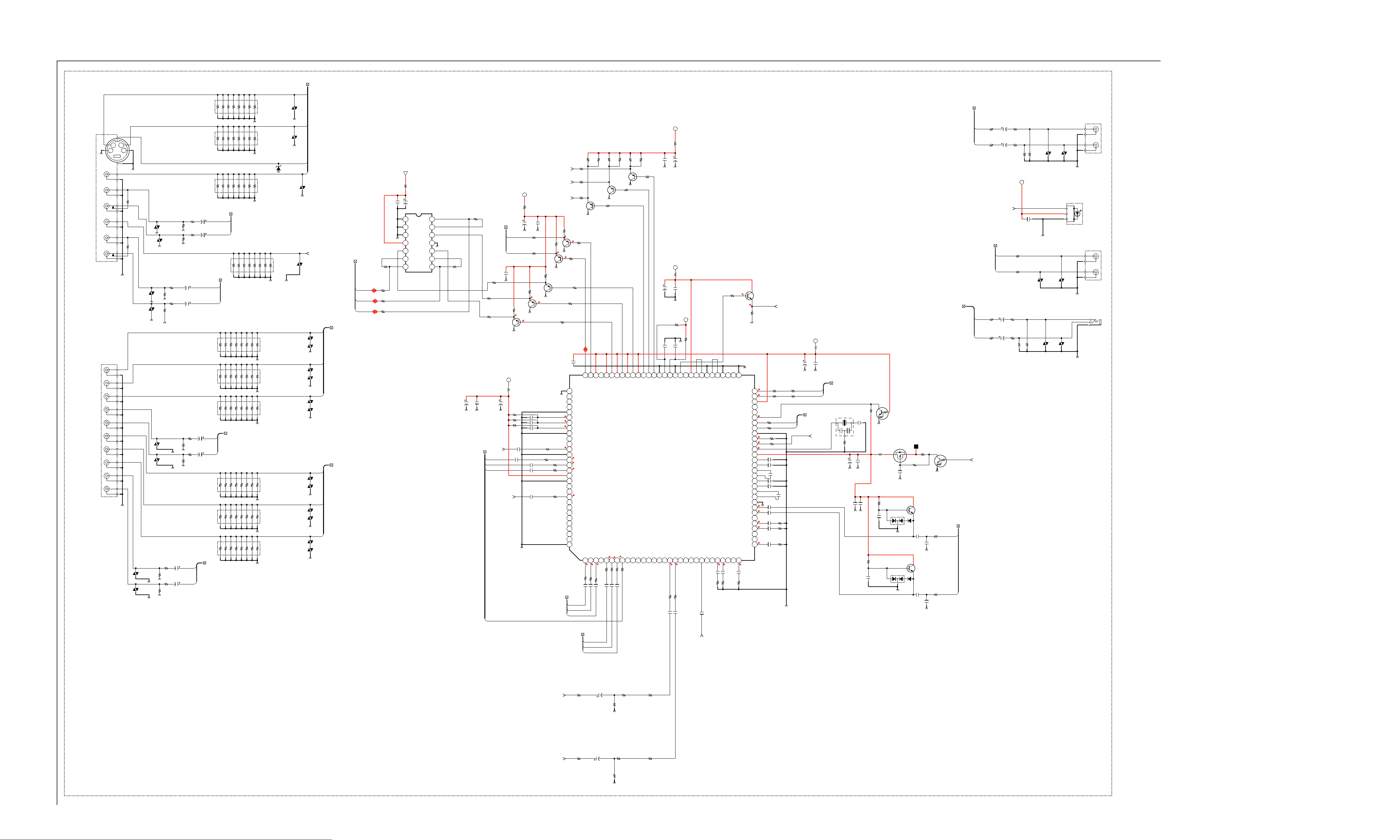
3-4. SCHEMATICS AND SUPPORTING INFORMATION
AU BOARD SCHEMATIC DIAGRAM (1 OF 6)
☛
1 | 2 | 3 | 4 | 5 | 6 | 7 | 8 | 9 | 10 | 11 | 12 | 13 | 14 | 15 | 16 | 17 | 18 | 19 | 20 | 21 | 22 | 23 | 24 |
KDL-52XBR4/52XBR5
A
—
B
—
C
—
D
—
E
—
F
—
G
—
H
—
I
—
J
—
K
—
L
—
To G
BALLANCER_ERR
INV_ERR
BL_ON
DIMMER
AC_RLY
PFC_DET(AC_DET)
PS_ERR
STBY_5V
CN001
12P
WHT
TO GF1 BOARD
CN6154
TO FB1 BOARD
CN4001
CN005
50P
BLK
GND
GND
ASUB_R
ASUB_L
GND
GND
REC_Y
REC_C
GND
GND
123456789
REC5V-BE
FL003
EMI
G
GND
REC5V
REC5V
GND
GND
C019
0.001
HDMI_STBY3.3V
STBY3.3V
AC_DET
GND
BL_ON
DIMMER
INV_FAIL1
BALLANCER_ERR
BL_IN
HP_DET
DSP_INT
DSP_MUTE2
DTT_PON
HDMI_WP
GND
GND
SET_ON2
SET_ON
BE_WDT
BE_RST
DDC_DET2
X_WDTRST
HPG_CTL
DDC_DET1
FE_SCL1
GND
FE_SDA1
GND
FE_SPDIF
EMMA2_AOBCK
EMMA2_AOLRCK
EMMA2_AOMCK
EMMA2_AOD2
EMMA2_AOD0
R062
R057
0
0
EMMA2_AOD2
EMMA2_AOMCK
R061
R058
0
0
EMMA2_AOD0
EMMA2_AOD1
R059
0
EMMA2_AOD1
1011121314151617181920212223242526272829303132333435363738394041424344454647484950
FB051
0uH
0uH
FB024
AC_DET
FB026
BL_ON
0uH
0uH
FB025
DIMMER
0uH
0uH
FB028
FB027
INV_FAIL
BALLANCER_ERR
BL_IN
0uH
FB029
0uH
FB030
HP_DET
0uH
0uH
FB032
FB031
DSP_INT
HDMI_DSP_MUTE2
0uH
FB035
REC_ON
0uH
FB033
HDMIPC_WP
0uH
FB037
BE_ON2
BE_ON
0uH
FB034
BE_WDT
R083
0
0uH
FB036
BE_RST
R041
R078
0
0
DTT_WDT
DDC5V_DET_1
R081
R076
0
0
DDC5V_DET_0
HDMI_HOTPLUG_CTRL
I2C_TAS_SCL_1
EMMA_SPDIF
I2C_TAS_SDA_1
R056
R060
0
0
EMMA2_AOBCK
EMMA2_AOLRCK
REC_Y
REC_C
GND
MAIN_COMP_OUT
MAIN_V_OUT
GND
GND
123
M_YS
M_CB/B
4
M_CB/B
M_CV/Y
56789
M_Y/CV
M_CR/R
M_CR/R
GND
GND
S_C
M_C
M_Y/G
M_Y/G
M_C
S_CR
12131415161718
10
11
S_C
S_CR
To TUU2
CN1001
CN003
50P
GND
1
TV_S_L
3
GND
5
TV_S_R
7
GND
9
SUB_H
11
GND
004:7D
TV_M_LR_IN
TV_M_L
TV_M_R
TUHSYNC_MAIN
V_DET
FB016
0uH
1
FB017
2
FB018
3
FB019
4
5
GND
GND
GND
18V
FB020
0uH
6
FB021
0uH
7
FB022
0uH
8
9
10
11
12
BALLANCER_ERR
0uH
0uH
0uH
FB045
0uH
INV_FAIL
BL_ON
DIMMER
AC_RLY
+B_OVP
C001
0.001
50V
X7R
1005
STBY5V
13
TV_S_V
15
GND
17
TV_M_L
19
0
R012
0
R013
0
R014
0
R016
C002
220
6.3V
GND
21
TV_M_R
23
GND
25
MAIN_H
27
GND
29
TV_M_V
31
GND
33
TV_GR_V
35
GND
37
FE_XRST
39
EWS_ALERT
41
AGC_MON
43
REC_ON
45
EWS_ON
47
GND GND
BRN
REC_3.3V
REC_3.3V
REC_3.3V
REC_3.3V
REC_6.5V
REC_6.5V
REC_6.5V
REC_6.5V
REC_6.5V
REC_6.5V
2
GND
GND
4
GND
6
8
10
12
14
GND
16
GND
18
GND
20
22
24
26
28
30
32
GND
34
GND
36
GND
38
12V
40
12V
42
12V
44
12V
46
GND
48
5049
AC_DET
R026
0
CHIP
1005
PFC_DET
C017
0.001
50V
X7R
1005
FL001
0uH
FB053
FB038
0uH
REC6.5V
EMI
G
12V
V2_V_IN
STBY3.3V
REC3.3V
1005
X7R
50V
0.001
C014
C010
0.001
50V
X7R
1005
STBY5V
TO FB1 BOARD
CN4002
BLK
80P
CN006
R084
0
BEM_RST
R087
0
BEM_RST
BEM_RX0
MODE_BEM
777879
R086
0
MODE_BEM
BEM_RX0
FE_I2C_0
BEM_SCL1
BEM_SDA1
R085
0
GND
FE_SCL0
FE_SDA0
GND
80
RB001
RB002
22
R117
22
BEM_TX3
BEM_RX3
STBY3.3V
R146
0
To JIG
GND
1
TV_TXD
2
TV_RXD
3
TV_FLASH_W
4
STBY3.3V
VD016
VD017
VD018
R115
22
22
RB004
VD019
VD020
RB003
22
22
VD021
VD026
VD022
VD027
VD023
VD028
VD024
VD029
VD025
VD030
5
TV_RST
6
DTT_LOG_RXD
7
LBM_UDP
8
LBM_UDM
9
LBM_VBUS
10
BEM_RST
11
DTT_LOG_TXD
12
NC
13
NC
14
BE_FLASH_W
15
BEM_RXD
16
BEM_TXD
17
GND
18
GND
1
AVC_LOG(TX)
2
AVC_LOG(RX)
3
BEM_LOG(TX)
4
BEM_LOG(RX)
5
E2TH_SCL_0(400)
6
E2TH_SDA_0(400)
7
BEM_SCL_1(400)
8
BEM_SDA_1(400)
9
BEM_SCL_2(100)
10
BEM_SCL_2(100)
11
BEM_SCL_3(400)
12
BEM_SDA_3(400)
13
E2TH_SCL_2_VSW
14
E2TH_SDA_2_VSW
15
GND
16
CN007
18P
CN008
16P
BLK
FE_SCL0
TV_EMMA_RX
FE_SDA0
BEM_SDA3
BEM_SDA2
BEM_SCL3
BEM_SCL2
GND
GND
BEM_SCL1
R092
0
BEM_SCL1
FE_SDA2
X_MDM_RST
UART2_DCD
UART2_RST
UART2_CTS
UART2_TX
UART2_RX
GND
GND
GND
CEC_ON
FAN_DRIVE1
FAN_ERR
R079
0
1005
CEC_ON
R074
0
R105
CHIP
0
0
BE_FAN_DRV1
FAN_DRIVE2
R104
0
*R106
BE_FAN_DRV2
41424344454647
TV_EMMA_UART
EPP(CCPM)_HS
DL_SI
DL_SCK
DL_CS
GND
GND
HDMI_INSEL2
HDMI_INSEL1
HDMI_INSEL4
HDMI_INSEL3
HDMI_SCL
HDMI_SDA
CEC_IN
GND
S_CV/Y
GND
GND
PC_H_OUT
PC_V_OUT
PC_H_IN
PC_V_IN
GND
S_Y/CV
PC_V_OUT
PC_H_OUT
19
PC_H_IN
C009
1005
GND
20212223242526
PC_V_IN
MAIN_H_SYNC
REC3.3V
FB006
0uH
0.1
16V
27282930313233
R048
R046
R050
R098
0
0
0
0
DL_CS
SPI_SI
SPI_SCK
8765
R073
0
HDMI_SEL_2
HDMI_SEL_1
R071
R077
0
0
HDMI_SEL_4
HDMI_SEL_3
CEC_OUT
34353637383940
R075
R080
0
0
CEC_IN
CEC_OUT
TV_EMMA_TX
48495051525354
R030
R033
0
0
TV_EMMA_TX
TV_EMMA_RX
FE_SCL0
FE_I2C_0
BEM_I2C_3
BEM_I2C_2
R027
R034
0
0
FE_SDA0
BEM_I2C_1
R096
0
56575859606162
55
R091
R094
R093
0
0
0
BEM_SCL3
FE_I2C_2
IC001
ADT75ARZ-REEL
4321
22
RB005
BEM_SCL2
BEM_SDA2
BEM_I2C_2
BEM_TX3
BEM_SDA1
FE_SCL2
EMMA_LOG_TX
63646566676869
R090
R029
R039
R036
0
BEM_SDA1
0
0
0
EMMA_LOG_TX
BEM_TX3
R088
0
EMMA_LOG_RX
BEM_RX3
R032
R089
0
0
EMMA_LOG_RX
BEM_RX3
GND
GND
LBM_DPLS
LBM_DMNS
70717273747576
R108
R109
0
0
LBM_DMNS
LBM_DPLS
BEM_I2C_3
FE_I2C_2
FE_SCL2
FE_SDA2
GND
BEM_I2C_2
GND
LBM_VBUS
R110
0
LBM_VBUS
TV_TXD
TV_RXD
TV_FLASH_M
JIG_RST
EMMA_LOG_RX
LBM_DPLS
LBM_DMNS
LBM_VBUS
BEM_RST
EMMA_LOG_TX
MODE_BEM
BEM_RX0
BEM_TX0
BEM_SCL3
BEM_SDA3
BEM_TX0
BEM_TX0
BEM_I2C_1
BEM_SCL2
BEM_SDA2
STBY_LED
ON_TIMER_LED
REC_LED
PMUTE_LED
M
—
N
—
O
—
FB052
0uH
To G
FB001
C003
0uH
470
16V
1234567
12V
12V
12V
C018
0.001
50V
X7R
1005
GND
GND
TO GF1 BOARD
CN6152
POWER_LED
0uH
FB047
REC5V
FL002
EMI
G
BE_ON
AUDIO_VCC
F001
5A
C004
24V
470
16V
C005
0.001
50V
X7R
1005
8
GND
GND
8P
CN002
AUDIO_VCC
AUDIO_VCC
0uH
FB023
123456789
NC
REC5V
BE_ON
CN7022
V2_L
0
R028
GND
GND
GND
V2_L
V2_V
V2_LR_IN
V2_R
HP_L
HP_R
001:8E
HP_LR_OUT
HP_DET
0.001C013
FB010
SIRCS
0uH
FB011
0uH
FB012
CHIP
R133 0
0uH
0uH
0uH
0uH
FB008
FB009
FB007
0uH
FB046
BL_IN
MAZ8056G0LS0D017
0
R031
0
R035
10111213141516171819202122232425262728293031323334353637383940
GND
V2_R
HP_L
0uH
0
R037
FB044
GND
GND
GND
GND
HP_R
HP_DET
STBY3.3V
LED_1(STBY)
LED_2(PMUTE)
TO HW3 BOARD
CN7152
LED_4(REC)
VED_5(POWER)
LED_3(TSUSHIN)
VD031
GND
SIRCS
BL_IN
REC_3.3V
TO HW1 BOARDTO HW2 BOARD
CN7001
POWER_SW
0uH
FB014
MAZ8056G0LS0
MAZ8056G0LS0
D019
D018
VD032
NC
GND
POWER_SW
0uH
VD033
0uH
FB015
KEY
FB048
KEY1
STBY5V
LOGO
LOGO
0uHFB002
AU 1/6
CONNECTORS
NC
GND
STBY3.3V
NC
IRO
GND
SET3.3V
40P
CN004
A-1231-638-A <FIX2>AU-P1
P
KDL-52XBR4/52XBR5 26
AU BOARD SCHEMATIC DIAGRAM (2 OF 6)
1 | 2 | 3 | 4 | 5 | 6 | 7 | 8 | 9 | 10 | 11 | 12 | 13 | 14 | 15 | 16 | 17 | 18 | 19 | 20 | 21 | 22 | 23 | 24 | 25 | 26 |
A
—
B
—
KDL-52XBR4/52XBR5
C
—
D
—
E
—
F
—
G
—
REC_ON
R201
10k
1/16W
CHIP
RT3WLMM-TP-1F
Q214
12V
3.15A
D201
MAZ8068G0LS0
R204
10k
1/16W
CHIP
3.15A
F201
24V
1/16W
R207
10k
1/16W
CHIP
R206
1k
CHIP
5%
C202
4.7
25V
X7R
3216
JL202
CHIP
R218
TAS3.3V
R306
R307
0
0
REC3.3V
CHIP
CHIP
IC208
PQ200WNA1ZPH
REC3.3V
REC9V
Vin
Vc
Vo
Vadj
12V
R281
C248
10k
CHIP
Q210
RT1N141C-TP-1
25V
2012
1
R283
CHIP
1/16W
R233
0
C223
C220
0
CHIP
0
R251
1608
1
16V
B
2012
R237
1
8.2k
25V
1/16W
RN-CP
0.5%
BD9853AFV
Vcc
OUT1_1
OUT1_2
VB
RT
FB1
-INE1
87654321
CSCP1 CSCP2
IC205
OUT2_1
OUT1_2
-INE2
1608
B
16V
16 15 14 13 12 11 10 9
VH
CTL
GND
FB2
C224
1
R249
0
JL212
R267
47k
1/16W
RN-CP
0.5%
JL213
R268
1/16W
RN-CP
0.5%
C233
22p
50V
CH
1005
56k
REC_ON
TAS3.3V
REC6.5V
REC6.5V
PQ070XNA1ZPH
IC210
R246
10k
C228
680p
50V
1005
R265
43k
R262
1/16W
RN-CP
0.5%
R266
270k
1/16W
RN-CP
0.5%
0
R258
10k
1/16W
RN-CP
B
0.5%
C227
0.015
16V
B
1005
12345
R287
10k
1/16W
CHIP
0
R289
0
CHIP
Q212
2SC3052EF-T1-LEF
GND
R291
4.7k
1/16W
RN-CP
0.5%
R292
100
1/16W
RN-CP
0.5%
R293
1k
1/16W
RN-CP
0.5%
R294
1k
1/16W
RN-CP
0.5%
C252
4.7
25V
X7R
3216
REC9V
SET9V
C254
4.7
25V
X7R
3216
R299
1005
C261
16V
0
47
SET9V_2
H
—
I
—
J
—
K
—
L
—
GND_1
C208
4.7
25V
X7R
3216
RSS040P03FD5TB
Q207
8765
5678
C229
3300p
50V
B
1234
4321
FB202
0uH
1608
R252
D205
1/10W
RN-CP
MA24D5000BS0
5%
1608
L203
10uH
C230
R260
C231
15
3300p
50V
B
1608
R259
15
15
1/10W
RN-CP
5%
1608
1/10W
RN-CP
5%
1608
4.7
25V
X7R
3216
FB206
D212
PTZ-TE25-6.8B
1608
R301
1608
CHIP
R300
CHIP
0
0
Vin
Vc
12345
C257
1
25V
2012
R302
1k
1/16W
CHIP
5%
PQ070XNA1ZPH
R305
1k
1/16W
RN-CP
0.5%
IC206
Vo
R303
680
1/16W
RN-CP
0.5%
R304
1/16W
RN-CP
0.5%
Vadj
GND
C259
10
10V
1k
X7R
3216
REC5V
TAS3.3V
REC5V
Vin
Vc
Vo
Vadj
GND
R269
1608
R270
1608
0
0
12345
C240
1
25V
2012
R276
390
1/16W
RN-CP
R273
1k
1/16W
CHIP
5%
R277
1k
1/16W
RN-CP
0.5%
0.5%
R275
2.7k
1/16W
RN-CP
0.5%
C244
10
10V
X7R
3216
REC5V-BE
M
—
N
—
O
—
R271
1608
R272
1608
0
0
R274
1k
1/16W
CHIP
5%
PQ070XNA1ZPH
IC207
Vin
Vc
Vo
Vadj
GND
12345
C241
25V
2012
R278
1
2.7k
1/16W
RN-CP
0.5%
*R308
CHIP
1608
C245
10
10V
X7R
3216
0
R279
390
1/16W
RN-CP
0.5%
R280
1k
1/16W
RN-CP
0.5%
REC5V-B
E
AU 2/6
POWER REGS
P
A-1231-638-A
KDL-52XBR4/52XBR5 27
<FIX2>AU-P2
AU BOARD SCHEMATIC DIAGRAM (3 OF 6)
1 | 2 | 3 | 4 | 5 | 6 | 7 | 8 | 9 | 10 | 11 | 12 | 13 | 14 | 15 | 16 | 17 | 18 | 19 | 20 | 21 | 22 | 23 | 24
KDL-52XBR4/52XBR5
A
—
B
—
C
—
D
—
E
—
F
—
G
—
H
—
I
—
J
—
K
—
L
—
M
VIDEO1
VIDEO3
COMP1
COMP2
6
34
4
3
S
12
12
J405
V1
L1
R1
V2
L2
R2
TB401
5
7
8
R415
9
0
CHIP
10
11
13
12
14
15
16
17
R416
0
CHIP
18
20
19
GRN
BLU
RED
WHT
RED
GRN
BLU
RED
WHT
RED
VD462
VD463
V
L
R
V
L
R
VD446
VD447
1/16W
R429
1M
1/16W
CHIP
5%
R430
1M
CHIP
5%
VD443
VD454
VD455
VD444
R439
1/16W
CHIP
1/16W
V1_IN
V1_YV1_Y
PC_LR_IN
Q423
HDMI_LR
PC_SYNC_IN
HDMI_L
HDMI_R
PC_AU_R
PC_AU_L
VSW_PW_CTRL
R599
0
CHIP
R600
0
CHIP
LINE_LR_OUT
R597
0
CHIP
R598
0
CHIP
LINE_L
LINE_R
C515
16V
C516
10
16V
C518
10
16V
OPT_OUT
10
C517
VD466
VD464
HDMI
VD467
VD465
L
R
J402
VIN
VCC
GND
TB404
3P
BLK
L
R
J403
10
16V
R443
2.2k
1/10W
RN-CP
0.5%
R444
2.2k
1/10W
RN-CP
0.5%
R604
R602
1M
1M
1/16W
1/16W
CHIP
CHIP
5%
5%
REC5V
C514
0.1
16V
1005
R617
0
CHIP
R618
0
CHIP
PC Audio
R445
2.2k
1/10W
RN-CP
0.5%
R446
2.2k
1/10W
RN-CP
0.5%
R601
1/16W
CHIP
VD468
VD469
R603
1M
1M
1/16W
CHIP
5%
5%
J404
600
RB401
600
RB402
D402
MAZ8100G0LS0
V1_V V1_V
600
RB403
V1_LR_IN
D1_L
D1_R
D2_LR_IN
V3_LR_IN
V3_L
V3_R
600
600
600
600
600
600
RB405
RB406
RB407
RB408
RB409
RB410
V1_L
V1_R
600
RB404
D1_LR_IN
R424
R431
1M
2.2k
C413
C412
16V
16V
10
10
R436
2.2k
1/10W
RN-CP
0.5%
R437
2.2k
1/10W
RN-CP
0.5%
D2_L
D2_R
1/10W
RN-CP
0.5%
R432
2.2k
1/10W
RN-CP
0.5%
C406
C407
C404
10
16V
C405
10
16V
10
16V
10
16V
1/16W
CHIP
5%
R425
1M
1/16W
CHIP
5%
R433
2.2k
1M
1/10W
RN-CP
0.5%
5%
R435
R440
2.2k
1M
1/10W
RN-CP
CHIP
0.5%
5%
R427
1M
1/16W
CHIP
5%
R428
1M
1/16W
CHIP
5%
R441
2.2k
C408
1/10W
10
RN-CP
16V
0.5%
R442
2.2k
C409
1/10W
10
RN-CP
16V
0.5%
VD440
V1_CV1_C
VD441
D1_CB
D1_CR
D2_Y D2_Y
D2_CB D2_CB
D1_Y
V1_SSW
VD445
VD442
VD448VD453VD458
VD449
VD450
VD451VD456VD461
VD452VD457
VD459
VD460
V3_V
D1_Y
D1_CB
D1_CR
D2_CRD2_CR
D1_V_IN
D2_V_IN
MAIN_COMP_OUT
M_CB/B
M_CR/R
M_Y/G
R447
1/10W
R448
1/10W
R449
1/10W
1/10W
68
68
68
R451
470
RN-CP
0.5%
C418
1608
0.1
25V
X7R
SET9V
R453
0
CHIP
C419
47
16V
OP-AMP
ADA4861-3YRZ-RL7
IC401
PD1
PD2
PD3
VCC
IN+1
654321
IN-1
7
OUT1 OUT3
REC5V
L404
10uH
1/10W
RN-CP
NC
CV/CR/R_IN7
3.6
3.6
1/16W100R541
1/16W
201216V2.2 X7R
R542
270
5%
CV/Y/G_OUT1_1
S1-3
5%
RN-CP
1/10W
270
R637
R548
22
1/16W
CHIP
5%
Q416
ISA1235AC1TP-1EF
BUFFER
R546
22
1/16W
CHIP
5%
NC
VCC5_OUT
C/CR/R_OUT2
C/CB/B_OUT1_1
C/CB/B_IN6
Y/Y/G_IN6
CV/CR/R_IN6
MD2/S2-2
C464
25V
2012
C470
47
16V
C471
1005
C/CB/B_OUT2
CV/Y/G_OUT2
CXA2240AR-TL
VIDEO SW
C/CB/B_IN5
Y/Y/G_IN5
1
0.1
16V
GND5_OUT
IC402
CV/CR/R_IN5
C472
Y_PH1
S1-2
201216V2.2 X7R
REC9V
L405
10uH
Y_PH2
C/CB/B_IN4
1/16WR613 100
R552
68k
1/16W
CHIP
5%
GND9_OUT
Y/Y/G_IN4
3.6
1/16WR614 100
C466
220
6.3V
C473
0.1
25V
X7R
1608
REC5V
C474
0.1
16V
1005
CV/Y_OUT3
CV/CR/R_IN4
3.6
201216V2.2 X7R
C475
VCC_9OUT
CV/Y_OUT4
S2-1
CV3
CHIP
R553
68k
1/16W
CHIP
CV_OUT5
CV2
5%
CV_SAG
CV1
C478
V_DET
NC
CV/Y_OUT5
S1-1
IN1_L3
C519
0.47
16V
X7R
1608
R557
100
1/16W
1005
5%
160816V1B
Y_SAG
IN1_V/L2
1.0
CHIP
NC
IN1_H/L1
C520
1.0
0.47
16V
X7R
1608
R558
100
1/16W
5%
R615
100
1/16W
CHIP
5%
C_OUT5
IN1_SW
4.7
4.0
0.5%
RN-CP
616263646566676869707172737475767778798081828384858687888990
ADR
DC_OUT
SDA
VCC5H_OUT
SELV_OUT2
SELH_OUT2
PC_ID
SELV_OUT1
SELH_OUT1
GND5H_OUT
IREF
PS_HVCS
EXT_CLK/X’tal
VCC_DEF
V_PH2
H_PH2
SYNC_IN2
SYNC_OUT2
V_PH1
H_PH1
SYNC_IN1
SYNC_OUT1
GND_DEF
IN4_H
IN4_V
IN3_SW
IN3_H/L1
IN3_V/L2
IN3_L3
IN2_SW
IN2_H/L1
IN2_L3
IN2_V/L2
C521
1.0
0.47
16V
X7R
1608
R587
100
1/16W
1005
SCL
1/16W
1005
Q424
2SC3052EF-T1-LEF
DATA_SLICER_MAIN
1k
R616
REC5V
L406
10uH
C499
0.1
16V
220
6.3V
FE_SCL2
FE_SDA2
PC_SYNC_OUT
PC_SYNC_INT
1005
FE_I2C_2
R589
0
CHIP
1005
X401
4MHz
C500
16V
R591
10k
1/16W
CHIP
5%
Q419
C507
1005
R590
10k
1/16W
CHIP
0.01
25V
X7R
5%
RT1N141C-TP-1
L407
10uH
R592
10k
1/16W
CHIP
5%
Q420
SI2301BDS-T1
S
C508
1
10V
X7R
1608
Q421
2SC3052EF-T1-LEF
D421
MC2838-T112-1
D423
MA2J1110GLS0
Q422
2SC3052EF-T1-LEF
D422
MC2838-T112-1
D424
MA2J1110GLS0
STBY5V
R593
3.3k
1/16W
CHIP
R594
10k
1/16W
CHIP
5%
5%
C509
10
10V
X7R
3216
C510
10
10V
X7R
3216
C512
1005
RT1N141C-TP-1
C511
47p
50V
CH
1005
47p
50V
CH
R595
470
1/16W
CHIP
5%
R596
470
1/16W
CHIP
5%
PC_H_IN
PC_V_IN
C502
0.1
16V
1005
C504
C503
1005
0.1
16V
1005
C505
0.01
0.1
25V
16V
X7R
1005
C506
0.01
25V
X7R
1005
47
60
59
58
57
56
55
54
53
52
51
50
49
48
47
46
45
44
43
42
41
40
39
38
37
36
35
34
33
32
31
CHIP
4.7
4.7
0.0
R572
0
R573
0
1.0
3.3
R575
2.9
C489
10V10X7R
1.0
C490 10
1.0
10V X7R
1.0
1.0
C492 0.47
16V X7R
1608
1.0
5%
C522
0.47
1608
C498
R578
47
1/16W
CHIP
R579
47
1/16W
CHIP
5%
10kR574
1/16W
10V1X7RC485
X7RC488
25V0.01
X7RC491
16V
X7R
5%
CHIP100
0.47
160816V
1/16W
C494
1608
0.1
100
1/16W
RN-CP
1005
R581
100
1/16W
R582
100
1/16W
CHIP
5%
1005
R586
1005
100516V
1005
C495
0.1
16V
CHIP
1005
R583
R584
PC_V_OUT
PC_H_OUT
0.5%
C486
0.01
1005
C487
1608
SIGN15050
5%
CHIP
0
CHIP
0
CHIP
25V
X7R
1
10V
X7R
5%
3.6
100
1/16W
R509
201216V2.2 X7R
C449
R537
1/10W
RN-CP
Q408
BUFFER
VCCFB_OUT
CV/CR/R_IN8
3.6
5%
RN-CP
270
1/10W
270
R638
5%
Q415
ISA1235AC1TP-1EF
BUFFER
R543
22
1/16W
CHIP
5%
FBLK_OUT
VCC5_OUT1
C/CR/R_OUT1_1
MD3/S2-3
C/CB/B_IN7
Y/Y/G_IN7
3.6
100R522
1/16W
100
100
1/16W
R530
R531
201216V2.2 X7R
201216V2.2 X7R
C454
C455
C456
5%
R532
RN-CP
270
1/10W
1/10W
270
RN-CP
R639
5%
S_C
R527
39
1/10W
RN-CP
0.5%
S_Y/CV
R528
39
1/10W
2.4
R475
CHIP
1/16W100
1/16W100
S_CR
22
3.6
3.6
3.6
3.6
100R498
D1_V_IN
RN-CP
0.5%
R529
39
1/10W
RN-CP
0.5%
Q414
ISA1235AC1TP-1EF
1.7
C453
16V
1005
R515
1/10W
RN-CP
2.4
R516
1/16W
CHIP
R481
1/16W
CHIP
0.1
91
92
93
94
95
96
97
98
99
100
101
102
103
104
105
106
107
108
109
110
111
112
113
114
115
116
117
118
119
120
BUFFER
330
5%
22
22
D1_CB
D1_Y
D1_CR
Q409
ISA1235AC1TP-1EF
BUFFER
1.7
R517
22
1/16W
CHIP
ISA1235AC1TP-1EF
R512
22
1/16W
CHIP
CV/Y
C_OUT1_2
NC
CV_OUT1_2
B_IN14
G_IN14
R_IN14
NC
CLP_CR2
CLP_CR1_1
CLP_CR1_2
FBLK_IN3
SC_B/C/CB/B_IN13
SC_G/Y/Y/G_IN13
SC_R/CV/CR/R_IN13
FBLK_IN2
3.6
SC_B/C/CB/B_IN12
3.6
SC_G/Y/YG_IN12
3.6
SC_R/CV/CR/R_IN12
VCC_IN
FBLK_IN1
SC_B/C/CB/B_IN11
SC_G/Y/Y/G_IN11
3.6
SC_R/CV/CR/R_IN11
MD4/S2-4
C/CB/B_IN10
Y/Y/G_IN10
CV/CR/R_IN10
S1-4
C/CB//B_IN9
Y/Y/G_IN9
CV/CR/R_IN9
GND_IN
C/CB/B_IN8
Y/Y/G_IN8
123456789101112131415161718192021222324252627282930
3.6
100
100
1/16W
1/16W
R507
R508
2012
201216V2.2 X7R
16V2 .2 X7R
C447
C448
D2_V_IN
D2_CB
D2_Y
D2_CR
REC5V
R510
L403
10uH
10V
M_C
M_Y/CV
2.4
Q403
BUFFER
0
CHIP
C450
1
100
25V
C458
2012
R476
1/10W
RN-CP
0.5%
R477
1/10W
RN-CP
0.5%
R478
330
1/10W
RN-CP
5%
Q406
2SA1226-T1E3E4
1.7
BUFFER
1608
X7R
25V0.1C438
10
R511
330
1/10W
RN-CP
5%
10
R486
330
1/10W
RN-CP
5%
1.7
R492
Q407
2SA1226-T1E3E4
BUFFER
160810V1 X7RC433
100
1/16W
R493
1/16W
100
R494
201216V2.2 X7RC439
R495
201216V2.2 X7RC440
201216V2.2 X7RC443
1/16W
160810V1 X7RC432
160810V1 X7RC434
1/16W
2.4
201216V2.2 X7RC437
R461
470
1/10W
RN-CP
14 13 12 11 10 9
OUT2
IN-2
IN+2
VEE
IN+3
IN-3
8
R455
470
1/10W
RN-CP
0.5%
0.5%
R466
1/10W
RN-CP
0.5%
R467
1/10W
RN-CP
0.5%
MAIN_V_OUT
C426
1
25V
2012
R465
10
1/10W
RN-CP
0.5%
10
R474
330
1/10W
RN-CP
5%
10
2SA1226-T1E3E4
REC5V
C425
1000
V1_IN
V1_C
V1_Y
V1_V
V1_SSW
V2_V_IN
6.3V
R471
R472
R473
1/16W330k
1/16W330k
1/16W330k
V3_V
6.3V
220
C526
1608
16V
0.068
C527
B
—
N
—
REC_C
R629
0.5%
RN-CP
1/10W
R627
R631
0
75
C524
0
100
10V
R632
0
AU 3/6
VIDEO SWITCH
INPUTS
O
REC_Y
—
P
KDL-52XBR4/52XBR5 28
R630
0.5%
RN-CP
1/10W
R628
R633
0
75
C525
0
100
10V
R634
0
A-1231-638-A
<FIX2>AU-P3
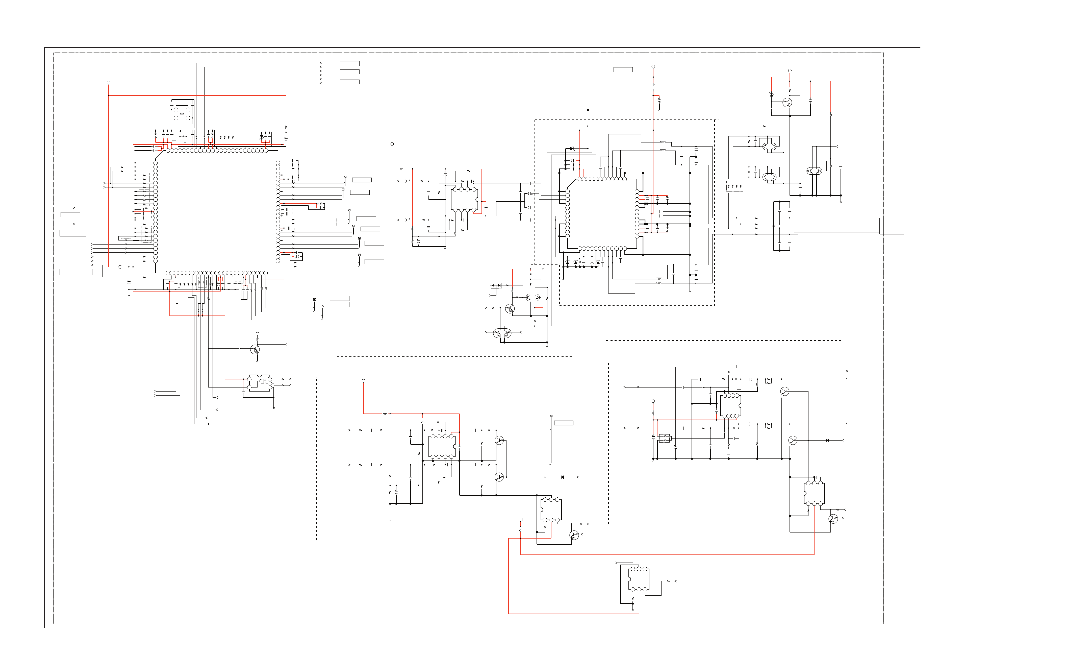
AU BOARD SCHEMATIC DIAGRAM (4 OF 6)
1 | 2 | 3 | 4 | 5 | 6 | 7 | 8 | 9 | 10 | 11 | 12 | 13 | 14 | 15 | 16 | 17 | 18 | 19 | 20 | 21 | 22 | 23 | 24 |
KDL-52XBR4/52XBR5
A
—
B
—
C
—
D
—
E
—
F
—
G
—
H
OPT_OUT
003:16C
OPT_OUT
EMMA_SPDIF
001:8E
EMMA2_OPT_IN
001:8C
EMMA2_AOD2
001:8C
EMMA2_AOD1
001:8E
EMMA2_AOD0
001:8E
EMMA2_AOLRCK
001:8E
EMMA2_AOBCK
001:8C
EMMA2_AOMCK
EMMA2_Digital IN
ATT_SW_LINE
ATT_SW_HP
TAS3.3V
RB807
47
MAX 300mA
3
1
C804
2012
FB803
A_HP_OUT_R
A_HP_OUT_L
A_SP_OUT_R
A_SP_OUT_L
A_LINE_OUT_R
A_LINE_OUT_L
C812
24.576MHz
12p CH
1005
C938
47
C809
6.3V
4.7
10V
C807
X7R
0.001
2012
50V
X7R
1005
C808
1
10V
X7R
1608
R815
1 23456789 101112131415161718192021222324 25
DVSS1
/VREG_EN
STEST
LS_LRCKOUT
LS_SCLKOUT
LS_SDOUT
LS_SDIN
MCLKOUT
LRCLKOUT
SCLKOUT
SDOUT1
SDOUT2/SPDIF_OUT
R813
47
DVDD2
VR_DIG1
DVSS2
R816
47
SPDIF_IN
SDIN1A
LRCLKINA
SCLKINA
MCLKINA
SDIN3
SDIN2
SDIN1
LRCLKIN
SCLKIN
47
RB811
10k
4
2
10k
RB801
100
RB810
RB804
10k
1
C805
25V
0.001
50V
C806
X7R
4.7
1005
6.3V
X6S
2012
RB803
10k
R824
47
R825
47
0uH
10V
100
C803
GND_1
50V
C811
6.3V
1005
C810
0.001
X6S
50V
X7R
1005
1
100
26
DVDD1
MCLKIN
C813
4.7
6.3V
X6S
2012
99
AVDD_OSC
DVSS3
27
C814
0.001
1005
X801
1
R833
220
R834
1M
97
98
VR_ANA
XTAL_OUT
I2C_SDA2
DVDD3
29
28
0 R835
50V
X7R
96
XTAL_IN
I2C_SCL2
30
0 R837
2
16V0.1C816
95
AVSS_ESD
I2C_SDA1
31
0 R838
94
AVDD_HP
I2C_SCL1
32
0 R839
C815
12p CH
1005
50V
A_HP_OUT_R
0 R842
92
93
HPOUTR
AVSS_HP
GPIO1
CS
34
33
R84310k
R84610k
C820
0.001
1005
A_HP_OUT_L
0 R850
91
HPOUTL
GPIO2
35
100
RB805
R84910k
50V
X7R
89
90
AVDD_HP
AUDIO DSP
CXD9890AQ
IC802
/MUTE
37
36
R854
10k
100 R853
AVDD_DAC
/RESET
R8551k
C821
47
6.3V
88
AVSS_DAC
DVSS4
38
C823
6.3V
47
R858 47
87
DACOUT2R
DVDD4
39
C824
0.001
1005
C831
2012
L803
10uH
4.7
10V
X7R
MAX 155mA
C832
100
10V
1C834
1C835
24kR871
C840
0.001
50V
X7R
C837
1005
47
C833
16V
1005
0.1
50V330pC846
PC_AU_R
PC_AU_L
50V330pC845
C839
6.3V
47
6.3V
D1_R
D1_L
R872 33k
R873 3 3k
6869707172737475
R874 33k
R875 33k
R878 33k
R879 33k
R880 33k
R881 33k
R882 33k
R883 3 3k
535455565758596061626364656667
5152
R884 33k
R885 33k
100516V0.1C838
D1_LR_IN
D2_LR_IN
D2_R
D2_L
HDMI_R
HDMI_L HDMI_L
C843
47
6.3V
C830
0.001
50V
D809
X7R
MAZ8056G0LS0
1005
R859 47
R860 47
R861 47
76
77
78
79
80
81
82
83
84
85
86
DACOUT2L
VR_DIG2
DVSS5
AVSS_ESD
42
41
40
C826
4.7
C955
6.3V
50V
330p
X6S
X7R
50V
2012
X7R
1005
LINEOUT1R
LINEIN1L
44
43
C956
330p
50V
X7R
1005
C828
4.7
10V
X7R
2012
LINEOUT1L
LINEIN1R
AVDD_LI
45
C829
0.001
50V
X7R
1005
LINEOUT2R
LINEIN2L
46
AVSS_LO
DACOUT1L
DACOUT1R
LINEOUT2L
LINEIN2R
47
R86633k
LINEOUT3R
AVSS_LI
48
R86833k
AVDD_REF
LINEOUT3L
V1P5_REF
BG_REF
BIAS_REF
AVSS_ADC/REF
AVDD_ADC
LINEIN10R
LINEIN10L
AVSS_LI
LINEIN9R
LINEIN9L
AVDD_LI
LINEIN8R
LINEIN8L
AVSS_LI
LINEIN7R
LINEIN7L
AVDD_LI
LINEIN6R
LINEIN6L
AVSS_LI
LINEIN5R
LINEIN5L
AVDD_LI
LINEIN4R
LINEIN4L
LINEIN3L
LINEIN3R
50
49
R87033k
R86933k
PC_LR_IN
C844
0.1
16V
C847
4.7
10V
X7R
2012
C848
10V
X7R 2012
D1/COMP1
D2/COMP2
HP_OUT
SP_OUT
LINE_OUT
HDMI_LR_IN
TV_M_R
TV_M_L
4.7
PC
TV_M_LR_IN
V2_LR_IN
V2_R
V2_L
V1_R
V1_L
V3_R
V3_L
HDMI ana
TV_M
VIDEO2
V1_LR_IN
V3_LR_IN
VIDEO1
VIDEO3
REC9V
A_SP_OUT_R
A_SP_OUT_L
L805
10uH
C856
C857
CHIP
1/16W
R892
1/16W
16V
16V
10k
CHIP
10k
R893
Audio_Vcc
JL802
MAZ8056G0LS0
D813
C888
C887
R910
6.8k
1/16W
RN-CP
R911
15k
1/16W
RN-CP
0.5%
V-
A+ IN
NJM4558V-TE2
IC805
B- IN
B+ IN
R908
10k
1/16W
5%
0.5%
C868
100p
50V
1005
AOUT
A- IN
BOUT
V+
8765
C867
100p
50V
CH
1005
R909
6.8k
1/16W
RN-CP
0.5%
AC_OFF_MUTE
SP_MUTE
C879
C881
0.001
22
R982
1/16W
CHIP
1/16W
10k
5%
R923
CHIP
47k
50V
X7R
1005
C880
0.001
50V
X7R
1005
R927
22k
1/16W
CHIP
R928
1/16W
CHIP
R920
10k
1/16W
CHIP
RT3WLMM-TP-1F
Q806
16V
C883
22
16V
C884
22
16V
C882
22
16V
22k
R930
47k
1/16W
CHIP
CH
C875
0.1
16V
1005
D806
MC2836
Q803
RT1N441C-TP-1
R979
10k
1/16W
CHIP
5%
1/16W
R905
CHIP
16V
47
C864
10k
5%
GND_1
4321
R907
15k
1/16W
RN-CP
0.5%
CHIP
R895
4.7k
1/16W
47
RN-CP
0.5%
C860
0.001
50V
X7R
1005
R898
4.7k
1/16W
RN-CP
47
0.5%
C861
0.001
50V
X7R
1005
C858
47
16V
C889
0.001
50V
X7R
1005
R931
47k
1/16W
CHIP
25V
1608
5%
0.1
X7R
100
25V
123456789101112
P1
GND
P2
RINN
P3
RINP
P4
AGND
P5
LINP
P6
LINN
P7
GAIN0
P8
GAIN0
P9
GAIN1
P10
MSTR/SLV
P11
SYNC
P12
GND
D811
MAZ8056G0LS0
D812
MAZ8056G0LS0
GND_1
R935
100k
RN-CP
0.5%
C893
0.22
25V
X7R
1608
P42
P43
P44
P45
P46
P47
P48
46
47
48
AVCC
AVCC
FAULT
VREG
ROSC
GND
15
14
13
P13
P14
C890
0.01
25V
X7R
1005
45
MUTE
VBYP
16
P15
P16
MAZ8056G0LS0
C891
47
16V
42
43
44
BSRP
ROUTP
SHUTDOWN
TPA3100D2PHPR
IC808
AUDIO AMP
BSLP
LOUTP
AGND
19
18
17
P17
P18
C894
0.22
25V
X7R
1608
D810
P19
C895
0.22
25V
X7R
1608
P37
P38
P39
P40
P41
37
38
39
40
41
GND
BSRN
ROUTN
ROUTN
ROUTP
LOUTP
LOUTN
21
20
P20
GND
PVCCR
PVCCR
PGNDR
PGNDR
VCLAMPR
VCLAMPL
PGNDL
PGNDL
PVCCL
PVCCL
GND
BSLN
LOUTN
GND
24
23
22
P21
P22
P23
P24
C896
0.22
25V
X7R
1608
AUDIO_VCC
12
22uH
L810
D803
C909
3300
25V
GND_1
L811
22uH
C914
0.22
C915
MPS
0.22
50V
MPS
C912
MPS
50V
0.22
50V
C913
MPS
0.22
RB802
100k
50V
L812
22uH
P36
P35
P34
P33
C897
P32
0.001
50V
X7R
P31
1005
P30
P29
P28
P27
P26
252627282930313233343536
C898
P25
0.001
50V
X7R
1005
L813
22uH
L814
22uH
C905
C899
0.1
1608
25V
X7R
C901
25V1
2012
C902
25V1
2012
C903
0.1
1608
X7R
25V
C906
220
35V
C907
0.22
50V
MPS
220
35V
C908
0.22
50V
MPS
GND_1
1/16W
7
2143658
TO DETECT
R946
120k
RN-CP
0.5%
C926
4.7
25V
X7R
3216
R947
120k
1/16W
RN-CP
0.5%
C927
4.7
25V
X7R
3216
R952
2012
R953
R955
2012
MAZ8082G0LS0
R951
6.8k
1/16W
CHIP
R948
100k
1/16W
CHIP
RT3AMMM
RT3AMMM
0
20120
R954
0
2012
0
Q809
Q810
Q811
RT1N141C-TP-1
C930
0.001
50V
X7R
1005
C931
0.001
50V
X7R
1005
REC9V
R958
10k
1/16W
CHIP
RT3N77M-TP-1
C934
0.1
25V
X7R
1608
C932
0.001
50V
X7R
1005
C933
0.001
50V
X7R
1005
Q828
C935
0.001
50V
X7R
1005
R960
100k
1/16W
CHIP
R961
1/16W
CHIP
SP_PROT
C937
47k
0.1
25V
X7R
1608
GND_1
R-
1
R+
2
L+
3
L-
4
CN801
4P
—
I
—
J
—
K
—
L
—
M
—
N
I2C_TAS_SDA_2
I2C_TAS_SCL_2
REGEL I2C
I2C_TAS_SCL_1
001:7B
I2C_TAS_SDA_1
001:7B
EMMA2 I2C
DSP_RST
DSP_INT
001:7C
C952
1005
16V
R976
1/16W
CHIP
0.1
100
5%
REC3.3V
R977
1k
1/16W
CHIP
5%
RT1N141C-TP-1
GND_1
IC813
TC7SZ32FU(TE85R)
54
VCC
GND
Q824
321
GND_1
R980
100
1/16W
CHIP
5%
R981
100
1/16W
CHIP
5%
1005
HDMI_MUTE
DSP_MUTE
HDMI_DSP_MUTE2
A_LINE_OUT_L
A_LINE_OUT_R
R998
1005
R997
1005
CHIP
CHIP
0
0
REC9V
C850
3216
C849
3216
10V
X7R
HDMI_MUTE
Q829
RT3N11M-TP-1
R899
15k
L804
10uH
10
R886
10V
5.6k
X7R
1/16W
RN-CP
R887
5.6k
1/16W
RN-CP
10
CHIP
1/16W
47k
R888
GND_1
C851
10
16V
CHIP
1/16W
47k
R889
1/16W
R894
47k
CHIP
5%
C855
2700p
C854
2700p
50V
1608
50V
1608
16V
47
C859
B
B
1/16W
RN-CP
0.5%
0.5%
RN-CP
1/16W
3.9k
R900
C862
330p
1005
B- IN
B+ IN
BOUT
IC804
NJM4558V-TE2
A- IN
A+ IN
V-
4321
R901
3.9k
1/16W
RN-CP
0.5%
R904
1/16W
RN-CP
0.5%
R903
47k
1/16W
CHIP
5%
R918
C870
2012
C871
2012
2.2k
1/16W
RN-CP
0.5%
2.2
10V
X7R
R915
470k
1/16W
CHIP
5%
R919
2.2k
2.2
1/16W
10V
RN-CP
CHIP
R916
470k
1/16W
0.5%
5%
X7R
Q804
DTC614TUT106
Q805
DTC614TUT106
50V
CH
8765
V+
C866
0.1
16V
1005
AOUT
C863
330p
50V
CH
1005
15k
F801
0.63A
32V
SHUTDOWN_MUTE
12V
GND_1
LINE_LR_OUT
LINE_L
LINE_R
OUT
R
123
R932
100k
1/16W
CHIP
5%
LINE_OUT
MA2J1110GLS0
456
GND
VCC
IN C
D807
RT8H225C
IC807
AC_OFF_MUTE
R933
3.3k
1/16W
CHIP
HDMI_MUTE
Q826
RT1N141C-TP-1
LINE_MUTE
A_HP_OUT_R
A_HP_OUT_L
R862
CHIP
1005
R863
CHIP
1005
HEADPHONE OUTPUT
C919
2.2
10V
X7R
2012
R938
R940
4.7k
10k
1/16W
1/16W
RN-CP
RN-CP
R939
1/16W
RN-CP
4.7k
0.5%
C920
0.001
50V
X7R
1005
C921
0.001
50V
X7R
1005
0.5%
C922
1005
0.1
16V
R941
47k
1/16W
CHIP
5%
0
REC9V
L809
10uH
0
C911
3
47
16V
1
RB808
10k
GND_1
C917
4.7
10V
X7R
2012
C918
4.7
10V
X7R
4
2012
2
C916
10
16V
R942
47k
1/16W
CHIP
5%
4321
V-
A+ IN
IC810
NJM3414AV(TE2)
B+ IN
B- IN
R944
47k
1/16W
RN-CP
0.5%
R943
10k
1/16W
RN-CP
0.5%
C923
2.2
10V
X7R
2012
C925
100p
50V
CH
1005
R945
47k
1/16W
RN-CP
0.5%
A- IN
AOUT
BOUT
V+
8765
C924
100p
50V
CH
1005
C929
R949
R956
10k
220
1/16W
1/10W
CHIP
RN-CP
5%
5%
R986
1/10W
RN-CP
R950
1/16W
CHIP
R969
220
1/10W
RN-CP
5%
Q812
DTC614TUT106
R957
220
1/10W
RN-CP
5%
220
5%
10k
5%
Q813
DTC614TUT106
R959
100k
1/16W
CHIP
5%
OUT
R
123
C936
GND
VCC
1608
0.1
25V
X7R
D808
MA2J1110GLS0
456
IN C
C928
47
16V
47
16V
IC811
RT8H225C
HP_OUT
HP_LR_OUT
HP_R
HP_L
AC_OFF_MUTE
R962
3.3k
1/16W
CHIP
HDMI_MUTE
Q827
RT1N141C-TP-1
HP_MUTE
—
AC_OFF_MUTE
O
—
OUT
R
123
R974
100k
1/16W
CHIP
5%
GND_1
456
GND
RT8H225C
VCC
IN C
IC812
R975
10k
1/16W
CHIP
PFC_DET
AU 4/6
AUDIO
P
A-1231-638-A
KDL-52XBR4/52XBR5 29
<FIX2>AU-P4
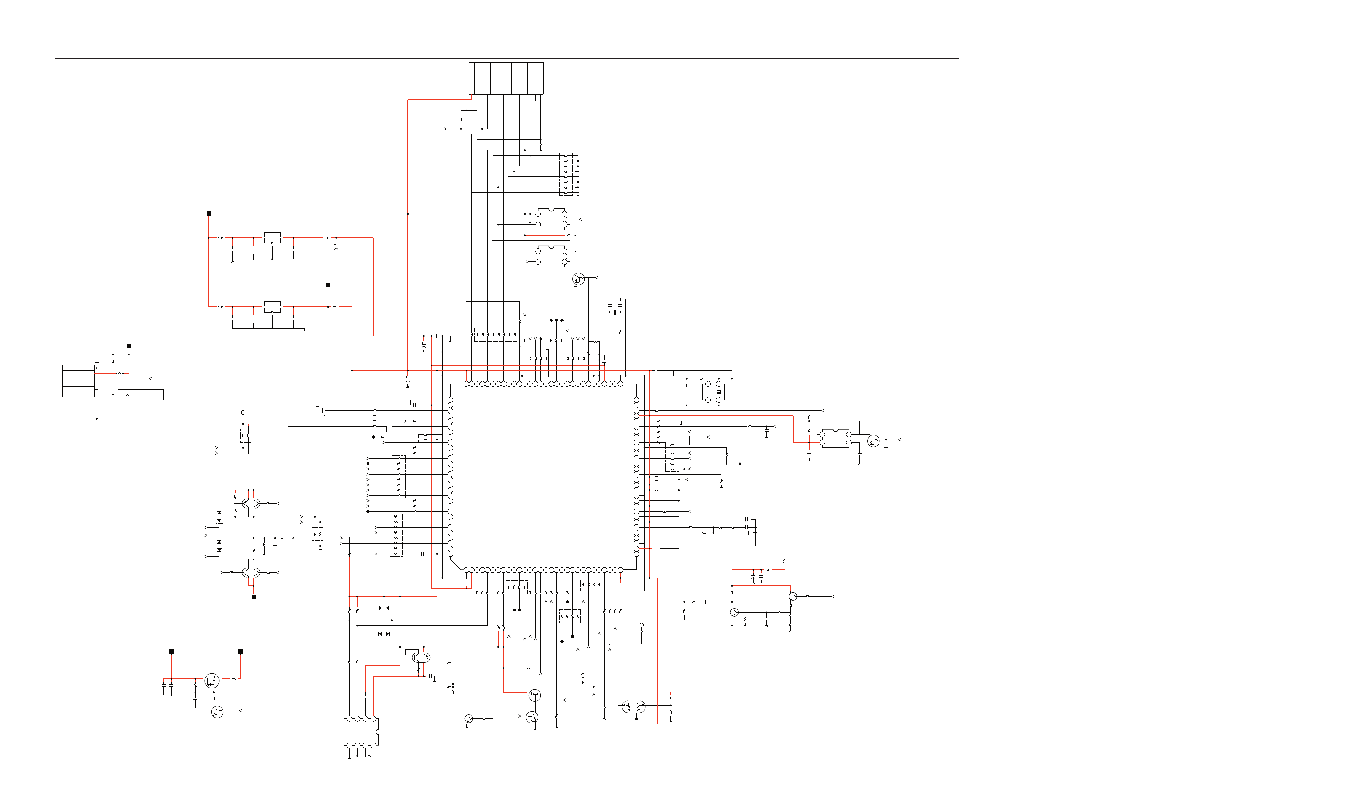
AU BOARD SCHEMATIC DIAGRAM (5 OF 6)
1 | 2 | 3 | 4 | 5 | 6 | 7 | 8 | 9 | 10 | 11 | 12 | 13 | 14 | 15 | 16 | 17 | 18 | 19 | 20 |
A
—
B
—
C
RESET
R1264
470
1/16W
CHIP
123456789
5%
UVCC
XTRST
XRSTIN
XINIT
BREAK
ICD3
ICD2
ICD1
ICD0
ICS2
1011121314
ICS1
ICS0
KDL-52XBR4/52XBR5
14P
CN1202
GND
ICLK
R1288
10k
1/16W
CHIP
5%
RB1203
10k
—
D
—
E
—
F
—
G
—
H
—
I
—
J
—
K
—
L
—
M
—
N
—
O
—
STBY3.3V
CN1201
6P
CEC_ON
RB1204
C1254
0.1
MC74VHC1G125DFT1
16V
ICD1
O_AC_RLY
JL1453
AC_RLY
Q1215
TV_TXD
47
1/16W
R1278
16V0.1C1229
X7R
1005
ICD0
TRSTX
O_EWS_ON
O_DTT_PON
JL1208
CHIP
100
R1281
HDMI_HOTPLUG_CTRL
5%
1/16W
O_HDMI_HOTPLUG_CTRL
O_REC_ON
REC_ON
R1280
10k
1/16W
CHIP
5%
X7R
1005
54
VCC
54
VCC
R1232
470
1/16W
MC74VHC1G125DFT1
CHIP
5%
CEC_IN
JL1209
CEC_OUT
5%
5%
CHIP
CHIP
CHIP1k
CHIP47
10k
1/16W5%
1/16W
100
1/16W5%
1/16W
R1291
R1283
R1286
R1289
I_CEC_IN
O_CEC_OUT
O_HDMI_HOTPLUG_CTRL2
IC1205
MB91F314APMC-G-101E1
RIGEL
O_BE_ON
O_BE_ON2
I_SIRCS
5%
5%
5%
5%
CHIP
CHIP
CHIP
CHIP
1k
100
100
100
1/16W
1/16W
1/16W
1/16W
R1292
R1287
R1284
R1290
BE_ON
BE_ON2
SIRCS
STBY5V
IC1202
3
0
C1210
1608
C1211
16V
1608
R1215
10k
1/16W
CHIP
5%
RT3AMMM
Q1221
1
16V
B
1
B
MM3121JPLE
I
VSS
IC1203
MM3123DPLE
I
VSS
R1213
10k
1/16W
CHIP 5%
1005
C1212
0.01
25V
X7R
1005
1005
5%
CHIP
1/16W
100k
R1214
O
O
C1214
KEY1
R1217
1/16W
DDC5V_DET_1
C1213
0.1
16V
1005
0.1
16V
1005
HDMI_SEL_1
HDMI_SEL_2
CHIP5%47
WAKE
L1201
10uH
C1206
0.1
16V
X7R
1005
L1202
10uH
C1207
0.1
16V
1005
STBY3.3V
C1201
R1207
0.1
10k
16V
1/16W
1005
CHIP
5%
1
GND
2
3
4
TX
5
GND
6
RX
GND_1
1005
L1452
0uH
R1203 1/16W5%100
CHIP
CEC_ON
CHIPR1202 1/16W 5%100
REC3.3V
2.2k
RB1215
R1211
100k
1/16W
CHIP
5%
R1212
10k
1/16W
CHIP
5%
1005
5%
CHIP
1/16W
100k
R1216
HDMI_STBY3.3V
R1363
1005
CHIP
0
214
Q1220
RT3AMMM
CEC_ON
R1235
HDMI_STBY3.3V
C1251
0.01
25V
X7R
1005
STBY3.3V
C1252
10V
X7R
3216
10
POWER_SW
PC_SYNC_INT
R1364
10k
1/16W
C1253
10
6.3V
X6S
2012
RT1N141C-TP-1
I2C_TAS_SDA_2
I2C_TAS_SCL_2
D1205
MC2836
D1206
MC2836
SIRCS
DDC5V_DET_0
RTR020P02TR
Q1217
S
Q1216
R1362
1/16W
CHIP
5%
1k
STBY1.8V
TV_EMMA_UART
10k
RB1216
L1203
10uH
C1218
47
6.3V
STBY3.3V
TV_EMMA_RX
TV_EMMA_TX
R1219
CHIP
TV_RXD
TV_TXD
0
HP_MUTE
JL1452
LINE_MUTE
SP_MUTE
SHUTDOWN_MUTE
STBY_LED
REC_LED
POWER_LED
ON_TIMER_LED
PMUTE_LED
JL1205
R1228
10k
1/16W
CHIP
5%
1005
R1220
R1222
2.2k
1/16W
1/16W
CHIP
5%
R1223
R1221
47
1/16W
1/16W
CHIP
5%
CLK
DAT
IC1204
M24C16-WMN6T(B)
EEPROM
4321
JL1451
HDMI_SEL_3
HDMI_SEL_4
HDMIPC_WP
D1213
MC2838-T112-1
2.2k
CHIP
5%
D1214
MC2836
47
CHIP
5%
R1225
10k
1/16W
CHIP
5%
WP
R1226
0
CHIP
RB1205
100
DSP_MUTE
8765
VCC
R1236
RB1208
100
RB1206
100
RB1207
100
1/16W
CHIP5%1k
RB1209
100
C1219
22
6.3V
WAKE
R1469
R1257
C1222
22
6.3V
R1233
CHIP
1/16W
5%10k
CHIP
1/16W
5%10k
R1237
R1238
R1247
R1248
R1249
Q1222
RT3WLMM-TP-1F
R1258
1k
1/16W
CHIP
5%
1/16W
47
1/16W
47
1/16W
1/16W
1/16W
1/16W
C1221
0.1C1220 X7R
0.1
16V
1005
X7R
C1225
0.1
16V
X7R
1005
C1223
0.1
16V
X7R
1005
GND
C1224
0.1
16V
1005
2SC3052EF-T1-LEF
R1260
1/16W
100
101
102
103
104
105
106
107
108
109
110
111
112
113
114
115
116
117
118
119
120
10k
91
92
1.8V
I_UART_Rx3
93
94
O_UART_Tx3
95
I_WAKE
96
I_UART_Rx4
97
O_UART_Tx4
98
I_EWS_ALERT
O_DSP_MUTE
99
IO_IIC_SDA5
IO_IIC_SCK5
O_HP_MUTE
O_MON_REC_MUTE
O_LINE_MUTE
O_SP_MUTE
O_SHUTDOWN_MUTE
O_STBY_LED
O_REC_LED
O_POWER_LED
O_TIMER_LED
O_PMUTE_LED
O_LAMP_LED
O_HDMI_SEL_1
O_HDMI_SEL_2
O_HDMI_SEL_3
O_HDMI_SEL_4
I_UART_Rx0
O_UART_Tx0
O_HDMIPC_WP
3.3V
C1227
16V
1005
X7R
R1259
1/16W
100k
CHIP
R1263
100k
1/16W
CHIP
1005
Q1208
0.1
5%
100516V
CHIP5%1k
CHIP5%100
CHIP5%100
CHIP5%100
47
RB1201
47
1/16W
R1265
3.3V
ICS2
ICLK
IBREAK
GND
1.8V
O_NVM_RST
IO_IIC_SDA1
123456789101112131415161718192021222324252627282930
5%
CHIP
CHIP47
100
1/16W
R1266
R1268
R1270
10k
1/16W
CHIP
5%
ICS1
IO_IIC_SCL1
CHIP47
R1269
ICS0
ICD3
O_NVM_WP
IO_IIC_SDA2
5%
CHIP
47
1/16W
R1272
5%
CHIP
10k
1/16W
R1273
47
RB1202
ICD2
IO_IIC_SCL2
5%
CHIP
47
1/16W
R1274
100
RB1210
5%
CHIP
10k
1/16W
R1275
RT1P141C-TP-1
Q1214
RT1N441C-TP-1
PFC_DET
001:4H
IC1208
OE
IN_A
GNDOUT_Y
OE
IN_A
GNDOUT_Y
IC1209
JL1228JL1229JL1230
5%
5%
CHIP
CHIP
CHIP
100
100
100
1/16W
1/16W
R1295
R1293
O_SPI_Tx9
O_SPI_SCK9
I_AVM_BUSY
O_VSW_PW_CTRL
O_CEC_ON/USUART_ON
I_AC_DET
5%
5%
CHIP
CHIP
1k
100
1/16W
1/16W
R1294
R1296
CEC_ON
VSW_PW_CTRL
RB1211
R1300
1/16W
5%
1/16W
R1297
100
JL1454
10k
CHIP
5%
O_AVM_CS
O_FE_RST
10k
321
321
SPI_SCK
5%
CHIP
CHIP47
100
1/16W5%
1/16W
R1301
R1303
O_SPI_SCK8
I_TUHSYNC_SUB
5%
CHIP
1k
1/16W
R1302
JL1212
JL1223
PFC_DET_MUTE
R1234
10k
1/16W
CHIP
SPI_SI
DL_CS
CHIP47
1/16W5%
R1305
O_DL_CS
I_SPI_Rx8
O_REC_RST
O_BE_RST
BE_RST
REC3.3V
R1285
10k
1/16W
CHIP
5%
1005
TV_RXD
Q1218
RT1N141C-TP-1
R1312
10k
LOGO
1/16W
CHIP
CHIP
5%
CHIP
1/16W
C1230
1k
0.1
R1309
100
1/16W
16V
X7R
1005
R1307
MD2
O_LOGO_LED
I_TUHSYNC_MAIN
I_BE_WDT
1k
RB1212
TUHSYNC_MAIN
BE_WDT
TV_FLASH_M
MD0 (L)
MD1 (L)
I_DTT_WDT
I_POWER_OVP
+B_OVP
DTT_WDT
C1232
18p
50V
CH
1005
C1231
0.1
16V
X7R
1005
1.8V
I_POWER_ERR
1k
RB1213
X1201
16.5MHz
R1315
1k
1/16W
CHIP
5%
MAIN_CLK_O
I_LAMP_IGN_INT
I_DDC5V_DET_1
I_CVHSYNC_MAIN
I_FAN_ERR
TV_FAN_ERR
R1360
10k
1/16W
CHIP
5%
C1233
616263646566676869707172737475767778798081828384858687888990
GND
SUB_CLK_I
MAIN_CLK_I
SUB_CLK_O
INITX
3.3V
O_FAN_DRV1
O_DSP_RST
I_POWER_KEY
O_DAC_RST
I_DDC5V_DET 0
I_TILT_DET
I_PC_SYNC_INT
I_AGC_MON
I_KEY
3.3(A/D)
3.3(A/D ref)
GND(A/D)
GND
3.3V
GND(DCK_PLL)
3.3V(DCk_PLL)
(CP_OUT)
(VCO_CTRL)
I_CV_MAIN(UC)
GND(SL)
3.3V(SL)
GND
I_SP_PROT
3.3V
C1234
004:17C
SP_PROT
22p
50V
1005
CH
0.1
60
59
58
57
56
55
54
53
52
51
50
49
48
47
46
45
44
43
42
41
40
39
38
37
36
35
34
33
32
31
R1322
10k
1/16W
CHIP
1005
100516V
X7R
5%
REC3.3V
Q1224
R1325
C1236
C1237
C1238
RT3T11M-TP-1
C1235
R1326
R1336
R1327
R1328
R1329
R1338
R1231
RB1214
1k
CHIP 5%
0.1
X7R
100516V
CHIP1k
1/16W 5%
1/16W
1/16W
1/16W
1/16W 5%
1/16W
10kR1210
CHIP5%1k
1/16W
1/16W
0.1
X7R
100516V
R1337
0.1
X7R
100516V
0.1
X7R
100516V
R1320
10k
1/16W
CHIP
5%
R1321
2.2k
1/16W
CHIP
5%
CHIP470
5%
1/16W
12V
CHIP5%1k
CHIP5%100
CHIP5%100
CHIP1k
CHIP5%10k
R1339
1/16W
CHIP5%1k
1/16W
R1261
1M
1/16W
CHIP
5%
1005
R1340
10M
1/16W
CHIP
1005
C1239
0.001
50V
1005
X7R
CHIP5%10k
32.768kHz
DSP_RST
DDC5V_DET_1
DDC5V_DET_0
KEY1
MAIN_H_SYNC
R1451
R1455
CHIP
R1342
X1202
PC_SYNC_INT
3.3k
1/16W
CHIP
R1452
CHIP
1005
0
220k
5%
CHIP
1/16W
POWER_SW
R1453
1/16W
RN-CP
0.5%
5%
0
C1451
0.1
16V
1005
Q1451
ISA1235AC1TP-1EF
C1241
8p
50V
CH
1005
1
C1242
9p
234
50V
CH
1005
R1352
1k
1/16W
CHIP
5%
R1353
2.2k
1/16W
CHIP
5%
R1464
1/16W
R1462
1005
R1463
1/16W
RN-CP
0.5%
0.5%
0
1k
0
C1243
0.01
25V
X7R
1005
C1456
0.1
16V
1005
C1457
100p
50V
CH
1005
L1451
10uH
C1453
0.1
2SC3052EF-T1-LEF
C1454
82p
50V
1005
TV_FAN_DRV
Q1452
R1460
4.7k
1/16W
0.5%
REC5V
R1461
1005
L1205
10uH
R1344
10k
1/16W
CHIP
5%
1005
JL1214
R1346
10k
1/16W
CHIP
5%
C1455
0.22
6.3V
X6S
R1454
1005
330
180
1/16W
RN-CP
0.5%
C1452
100
10V
R1456
560
1/16W
1005
0.5%
R1458
10k
1/16W
0.5%
RESET
RESET
IC1206
PST3629UL
12
GND
VDD C
C1244
0.1
16V
X7R
1005
33
43
OUT
C1246
0.1
16V
X7R
1005
DATA_SLICER_MAIN
Q1213
RT1N141C-TP-1
C1247
1005
JIG_RST
0.1
16V
AU 5/6
SUB MICRO
P
A-1231-638-A
KDL-52XBR4/52XBR5 30
<FIX2>AU-P5
 Loading...