

Page 1
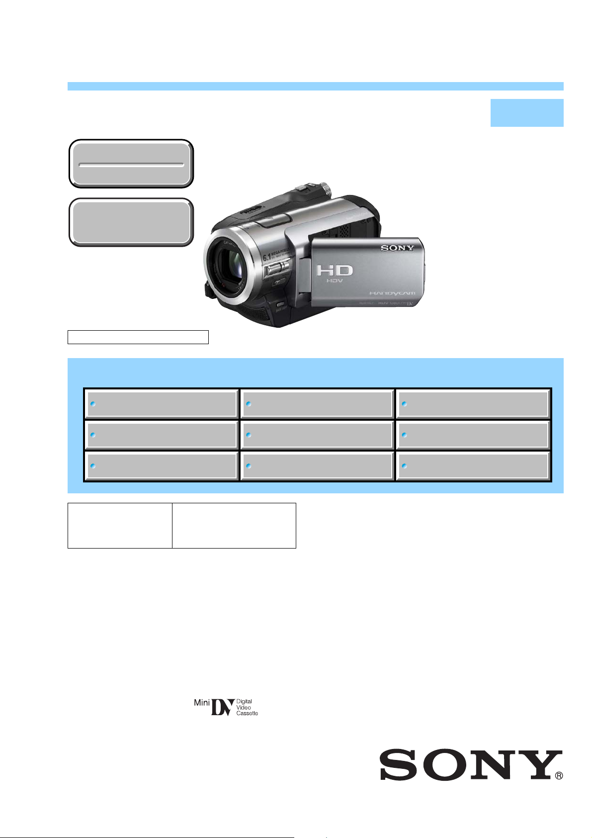
HDR-HC5/HC5E/HC7/HC7E
RMT-831
SERVICE MANUAL
Ver. 1.4 2008.06
Revision History
Revision History
How to use
How to use
Acrobat Reader
Acrobat Reader
N MECHANISM (MDX-N110)
Link
Link
SPECIFICATIONS
DISASSEMBLY
Photo: HDR-HC7
LEVEL 2
US Model
Canadian Model
AEP Model
UK Model
East European Model
North European Model
E Model
Australian Model
Chinese Model
Hong Kong Model
Korea Model
Tourist Model
Japanese Model
SCHEMATIC DIAGRAMS
MODEL INFORMATION TABLE
SERVICE NOTE
The components identified by
mark 0 or dotted line with
mark 0 are critical for safety.
Replace only with part number specified.
BLOCK DIAGRAMS
FRAME SCHEMATIC DIAGRAMS
Les composants identifiés par une
marque 0 sont critiques pour la
sécurité.
Ne les remplacer que par une pièce
portant le numéro spécifié.
DIGITAL HD VIDEO CAMERA RECORDER
PRINTED WIRING BOARDS
REPAIR PARTS LIST
HDR-HC5/HC5E/HC7/HC7E_L2
Sony EMCS Co.
2008F0500-1
© 2008.6
Published by Kohda TEC9-852-176-31
Page 2

SPECIFICATIONS
ENGLISH JAPANESE
ENGLISH JAPANESE
System
Focal length
Video recording system (HDV)
2 rotary heads, Helical scanning system
Video recording system (DV)
2 rotary heads, Helical scanning system
Still image recording system
Exif Ver. 2.2*
1
Audio recording system (HDV)
Rotary heads, MPEG-1 Audio Layer -2,
Quantization: 16 bits (Fs 48 kHz,
stereo)
transfer rate: 384 kbps
Audio recording system (DV )
Rotary heads, PCM system
Quantization: 12 bits (F s 32 kHz, stereo
1, stereo 2), 16 bits (Fs 48 kHz, stereo)
Video signal
HDR-HC5/HC7:
NTSC color, EIA standards
1080/60i specificatio n
HDR-HC5E/HC7E:
PAL color, CCIR standards
1080/50i specification
Usable cassette
Mini DV cassette with the mark
printed
Color temperature
Tape speed (HDV)
Approx. 18.81 mm/s
Tape speed (DV)
SP: Approx. 18.81 mm/s
Minimum illumination
LP: Approx. 12.56 mm/s
Recording/playback time (HDV)
60 min (using a DVM60 cassette)
Recording/playback time (DV)
SP: 60 min (using a DVM60 cassette)
LP: 90 min (using a DVM60 cassette)
Fast forward/rewind time
Approx. 2 min 40 s (using a DVM60
cassette and rechargeable ba ttery pack)
Approx. 1 min 45 s (using a DVM60
cassette and AC Adaptor)
Viewfinder
Electric viewfinder (color)
Image device
HDR-HC5/HC5E:
5.9 mm (1/3 type) CMOS sensor
Recording pixels (still, 4:3):
Max. 4.0 mega (2 304 × 1 728) pixels*
2
Gross: Approx. 2 100 000 pixels
Effective (movie, 16 :9):
Approx. 1 430 000 pixels
Effective (movie, 4:3):
Approx. 1 080 000 pixels
Effective (still, 16: 9):
Approx. 1 490 000 pixels
Effective (still, 4:3) :
Approx. 1 990 000 pixels
Input/Output connectors
Audio/Video output
HDR-HC7/HC7E:
6.3 mm (1/2.9 type) CMOS sensor
Recording pixels (still, 4:3):
Max. 6.1 mega (2 848 × 2 136) pixels*
2
Gross: Approx. 3 200 000 pixels
Effective (movie, 16 :9):
Approx. 2 280 000 pixels
Effective (movie, 4:3):
Approx. 1 710 000 pixels
Effective (still, 16: 9):
Approx. 2 280 000 pixels
Effective (still, 4:3) :
Approx. 3 040 000 pixels
Lens
HDR-HC5/HC5E:
Carl Zeiss Vario-Sonnar T
10 × (Optical), 20 ×, 80 × (Digital)
HDR-HC7/HC7E:
Carl Zeiss Vario-Sonnar T
10 × (Optical), 20 × (Digital)
COMPONENT OUT jack
HDR-HC5/HC5E/HC7/HC7E_L2
HDR-HC5/HC5E:
f=5.1 ~ 51 mm (7/32 ~ 2 1/8 in.)
When converted to a 35 mm still
camera
In CAMERA-TAPE *
3
: 41.3 ~ 485mm
(1 11/16 ~ 19 1/8 in.) (16:9), 50.5 ~
594 mm (2 ~ 23 1/2 in.) (4:3)
In CAMERA-MEMORY: 40.4 ~
404 mm (1 5/8 ~ 16 in.) (16:9), 37 ~
370 mm (1 1/2 ~ 14 5/8 in.) (4:3)
F1.8 ~ 2.9
Filter diameter: 37 mm (1 1/2 in.)
HDR-HC7/HC7E:
f=5.4 ~ 54 mm (7/32 ~ 2 1/4 in.)
When converted to a 35 mm still
camera
In CAMERA-TAPE: 40 ~ 400 mm
(1 5/8 ~ 15 3/4 in.) (16:9), 49 ~ 490 mm
(1 15/16 ~ 19 3/8 in.) (4:3)
In CAMERA-MEMORY: 40 ~ 400 mm
(1 5/8 ~ 15 3/4 in.) (16:9), 37 ~ 370 mm
(1 1/2 ~ 14 5/8 in.) (4:3)
F1.8 ~ 2.9
Filter diameter: 37 mm (1 1/2 in.)
[AUTO], [ONE PUSH], [INDOOR]
(3 200 K),
[OUTDOOR] (5 800 K)
HDR-HC5/HC7:
2 lx (lux) ([AUTOSLW SHTR] [ON],
Shutter speed 1/30 sec)
0 lx (lux) (during NightShot function)
HDR-HC5E/HC7E:
2 lx (lux) ([AUTOSLW SHTR] [ON],
Shutter speed 1/25 sec)
0 lx (lux) (during NightShot function)
*1“Exif” is a file format for still images,
established by the JEITA (Japan
Electronics and Information Technology
Industries Association). Files in this
format can have addition al information
such as your camcorder’s setting
information at the time of recording.
2
*
The unique pixel array of Sony’s
ClearVid CMOS sensor and image
processing system (new Enhanced
Imaging Processor) allows for still
image resolution equivalent to the sizes
described.
3
*
The focal length figures are actual
figures resulting from wide angle pixel
read-out.
HDR-HC5/HC7:
10-pin connector
Video signal: 1 Vp-p, 75 Ω (ohms)
Luminance signal: 1 Vp-p, 75 Ω (ohms)
Chrominance signal: 0.286 Vp-p, 75 Ω
(ohms)
Audio signal: 327 mV (at load
impedance 47 kΩ (kilohms)), Output
impedance with less than 2.2 kΩ
(kilohms)
HDR-HC5E/HC7E:
10-pin connector
Video signal: 1 Vp-p, 75 Ω (ohms)
Luminance signal: 1 Vp-p, 75 Ω (ohms)
Chrominance signal: 0.3 Vp-p, 75 Ω
(ohms)
Audio signal: 327 mV (at load
impedance 47 kΩ (kilohms)), Output
impedance with less than 2.2 kΩ
(kilohms)
Y: 1 Vp-p, 75 Ω (ohms)
B/PR
, CB/CR: ± 350 mV, 75 Ω (ohms)
P
— 2 —
HDMI OUT jack
TypeA (19-pin)
Headphone jack (HDR-HC7/HC7E)
Stereo minijack (Ø 3.5 m m)
LANC jack
Stereo mini-minijack (Ø 2.5 mm)
USB jack
mini-B
MIC (PLUG IN POWER) jack
(HDR-HC7/HC7E)
Stereo minijack (Ø 3.5 m m)
HDV/DV jack
i.LINK Interface (IEEE1 394, 4-pin
connector S100)
LCD screen
Picture
6.9 cm (2.7 type, aspect ratio 16:9)
Total dot number
211 200 (960 × 220)
General
Power requirements
DC 6.8 V/7.2 V (battery pack)
DC 8.4 V (AC Adaptor)
Average power consumption
HDR-HC5:
During camera recording us ing the
viewfinder with normal brightness:
HDV recording 3.8 W
DV recording 3.5 W
During camera recording us ing the
LCD with normal brightness:
HDV recording 4.1 W
DV recording 3.8 W
HDR-HC5E:
During camera recording using the
viewfinder with normal brightness:
HDV recording 3.6 W
DV recording 3.3 W
During camera recording using the
LCD with normal brightness:
HDV recording 3.9 W
DV recording 3.6 W
HDR-HC7:
During camera recording us ing the
viewfinder with normal brightness:
HDV recording 4.2 W
DV recording 4.0 W
During camera recording us ing the
LCD with normal brightness:
HDV recording 4.5 W
DV recording 4.3 W
HDR-HC7E:
During camera recording using the
viewfinder with normal brightness:
HDV recording 4.0 W
DV recording 3.8 W
During camera recording using the
LCD with normal brightness:
HDV recording 4.3 W
DV recording 4.1 W
Operating temperature
0 °C to + 40 °C (32 °F to 104 °F)
Storage temperature
-20 °C to + 60 °C (-4 °F to + 140 °F)
Dimensions (approx.)
HDR-HC5/HC5E:
82 × 82 × 134 mm
(3 1/4 × 3 1/4 × 5 3/8 in.) (w/h/d)
including the projecting parts
82 × 82 × 134 mm
(3 1/4 × 3 1/4 × 5 3/8 in.) (w/h/d)
including the projecting part s w it h the
supplied battery pack NP-FH60
attached
HDR-HC7/HC7E:
82 × 82 × 138 mm
(3 1/4 × 3 1/4 × 5 1/2 in.) (w/h/d)
including the projecting parts
82 × 82 × 138 mm
(3 1/4 × 3 1/4 × 5 1/2 in.) (w/h/d)
including the projecting part s w it h the
supplied battery pack NP-FH60
attached
Mass (approx.)
HDR-HC5/HC5E:
530 g (1 lb 2 oz) main unit only
630 g (1 lb 6 oz) including the N P FH60 rechargeable battery pack and
DVM60 cassette.
HDR-HC7/HC7E:
550 g (1 lb 3 oz) main unit only
650 g (1 lb 6 oz) including the N P FH60 rechargeable battery pack and
DVM60 cassette.
Supplied accessories
AC Adaptor (1)
Power cord (1)
Wireless Remote Commander (1)
A/V connecting cable (1)
Component video cable (1)
i.LINK cable (1)
USB cable (1)
Rechargeable battery pack NP-FH60 (1)
CD-ROM “Handycam Application
Software” (1)
Operating Guide (1)
See page 5-38.
AC Adaptor AC-L200/L200B
Power requirements
AC 100 - 240 V, 50/60 Hz
Current consumption
0.35 - 0.18 A
Power consumption
18 W
Output voltage
DC 8.4 V*
Operating temperature
0 °C to + 40 °C (32 °F to 104 °F)
Storage temperature
-20 °C to + 60 °C (-4 °F to + 140 °F)
Dimensions (approx.)
48 × 29 × 81 mm (1 15/16 × 1 3/16 ×
31/4 in.) (w/h/d) excluding the
projecting parts
Mass (approx.)
170 g (6.0 oz) excluding the power cord
* See the label on the AC Adaptor for other
specifications.
Rechargeable battery pack (NP-FH60)
Maximum output voltage
DC 8.4 V
Output voltage
DC 7.2 V
Capacity
7.2 Wh (1 000 mAh)
Dimensions (approx.)
31.8 × 33.3 × 45.0 mm
(1 5/16 × 1 5/16 × 1 13/16 in.) (w/h/d)
Mass (approx.)
80 g (2.9 oz)
Operating temperature
0 °C to + 40 °C (32 °F to 104 °F)
Type
Lithium ion
Design and specifications are subject to change
without notice.
Page 3

概略仕様
ENGLISH JAPANESE
ENGLISH JAPANESE
システム
録画方式
(
)
HDV
録画方式
)
(
DV
静止画記録方
式
録音方式
)
(
HDV
録音方式
(
)
DV
映像信号
使用可能カ
セット
テープ速度
)
(
HDV
テープ速度
(
)
DV
再生時
録画
/
)
間(
HDV
録画
再生時
/
間(
)
DV
早送り、
巻き戻し時間
ファインダー 電子ファインダー:カラー
撮像素子
ズームレンズ カール ツァイス バリオゾナー
2
ヘッドヘリカルスキャン
回転
回転
2
ヘッドヘリカルスキャン
Exif Ver.2.2*
回転ヘッド
MPEG-1 Audio Layer2
ビット
16
転送レート
回転ヘッド
ビット
12
(ステレオ1、ステレオ2)
ビット
16
NTSC
1080/60i
セット
約
18.81mm/
:約
SP
:約
LP
分(
60
SP:60
LP:90
バッテリー使用時:
約
2分40
AC
約
1分45
6.3mm(1/2.9
サー
記録画素数:静止画時最大
画素相当
モード)
3
総画素数:約
動画時有効画素数(
ド):約
動画時有効画素数(
約
171
静止画時有効画素数(
ド):約
静止画時有効画素数(
ド):約
1
(ステレオ)
48kHz
384kbps
32kHz
(ステレオ)
48kHz
カラー、
マークのついたミニ
18.81mm/
12.56mm/
DVM60
分(
分(
アダプター使用時:
228
万画素
228
304
標準方式
EIA
方式
秒
秒
秒
使用時)
使用時)
DVM60
使用時)
DVM60
秒(
DVM60
秒(
DVM60
型)
CMOS
2
(
*
2848 × 2136
万画素
320
16:9
万画素
4:3
万画素
万画素
使用時)
使用時)
16:9
4:3
モード):
T
倍(光学)、20倍(デジタル)
10
f=5.4〜54mm
カメラ換算では
35mm
「撮る−テープ」時:
40〜400mm(16:9
モードでは49〜
(
4:3
「撮る−メモリー」時:
40〜400mm(16:9
(
モードでは37〜
4:3
F1.8〜2.9
フィルター径
モード)
490mm
モード)
370
37mm
DV
セン
610
モー
モー
モー
mm)
カ
万
)(4:
)
色温度切り換え[オート]、[ワンプッシュ]、
最低被写体照
度
1
*
(社)電子情報技術産業協会(
された、撮影情報などの付帯情報を追加する
ことができる静止画用のファイルフォーマッ
ト。
2
*
ソニー独自のクリアビッド
画素配列と画像処理システム新エンハンスド
イメージングプロセッサーにより、静止画は
表記の記載サイズを実現しています。
出力端子
入
/
A/V OUT
端子
コンポーネン
トビデオ端子
HDMI OUT
端子
ヘッドフォン
端子
LANC
USB
MIC
HDV/DV
子
[屋内](
[屋外](
(ルクス)([オートスロー
5 lx
シャッター][入]、[シャッタース
ピード]
(ルクス)(
0 lx
3 200K
5 800K
秒)
1/30
)、
)
NightShot
JEITA
CMOS
ピン特殊コネクター
10
映像:
1 Vp-p、75
出力
Y
出力
C
音声:
327mV(47k
力インピーダンス
D1/D3
オ端子
Y:1Vp-p、75
PB/PR. CB/C
タイプ
A(19
ステレオミニジャック(
端子 ステレオミニミニジャック
端子
入力端子 ステレオミニジャック(
端
)
(
ø 2.5
mini-B
i.LINK(IEEE1394 4
クター
Ω
1Vp-p、75
0.286Vp-p、75
Ω
Ω負荷時)、出
2.2k
映像:コンポーネントビデ
Ω
:±
R
350mV、75
ピン)
)
S100
時)
)にて制定
センサーの
Ω
Ω以下
ø 3.5
ø 3.5
ピンコネ
液晶画面
画面サイズ
総ドット数
6.9cm(2.7
16:9
211 200
横
960
)
×縦
型、アスペクト比
ドット
220
電源部、その他
電源電圧 バッテリー端子入力
消費電力 ファインダー使用時、明るさ標
端子入力
DC
準:
記録時
HDV
記録時
DV
液晶画面使用時、明るさ標準:
記録時
HDV
記録時
DV
8.4V
4.2W
4.0W
4.5W
4.3W
6.8V/7.2V
)
)
Ω
動作温度
保存温度 −
外形寸法
本体質量 約
撮影時総質量 約
付属品
℃〜
0
82×82×138mm
(最大突起部を含む)(幅×高さ×
奥行き)
82×82×138mm
(突起部含む、付属バッテリー
パック
テープ(
AC
電源コード(
ワイヤレスリモコン(
AV
D
ケーブル(
i.LINK
USB
リチャージャブルバッテリー
パック
℃
+40
℃〜
20
550g
650g
アダプター(1)
接続ケーブル(1)
端子コンポーネントビデオ
℃
+60
NP-FH60
ケーブル(1)
装着状態)
(本体のみ)
(バッテリー
)含む。)
DVM60
1
)
1
)
ケーブル(1)
NP-FH60(1
NP-FH60、
1
)
)
CD-ROM「Handycam
Application Software
取扱説明書(
保証書(
アダプター
AC
電源
消費電力
定格出力
動作温度
保存温度 −
外形寸法 約
質量 約
その他の仕様についてはACアダプターのラ
*
ベルをご覧ください。
AC100〜240V、50/60Hz
18W
DC8.4V *
℃〜
0
20
48×29×81mm
をのぞく)(幅×高さ×奥行き)
170g
1
1
)
AC-L200/L200B
℃
+40
℃〜
+60
(本体のみ)
」(1)
)
℃
(最大突起部
リチャージャブルバッテリーパック
NP-FH60
最大電圧
公称電圧
容量
最大外形寸法 約
質量 約
使用温度
使用電池
本機の仕様および外観は、改良のため予告なく
変更することがありますが、ご了承ください。
DC8.4V
DC7.2V
7.2Wh(1000mAh
31.8×33.3×45.0mm
(幅×高さ×奥行き)
80g
℃〜
+40
℃
0
Li-ion
)
HDR-HC5/HC5E/HC7/HC7E_L2
— 3 —
Page 4

Model information table
Model HDR-HC5 HDR-HC5E HDR-HC7 HDR-HC7E
Destination US, CND, E, KR,
AEP, UK, EE, NE,
E, AUS, CH, HK AUS, CH, HK, JE
US, CND, E, KR, JE, J
Color system NTSC PAL NTSC PAL
Recording pixels (Max.) 4.0M pixels 4.0M pixels 6.1M pixels 6.1M pixels
Steadyshot electronic electronic optical optical
HP jack/MIC jack ××aa
Camera control dial/
Manual button
××aa
CM board CM-076 CM-076 CM-077 CM-077
FP-647 flexible board ××aa
Control switch block
(AD11800)
•Abbreviation
AR : Argentine model
AUS: Australian model
BR : Brazilian model
CH : Chinese model
CND: Canadian model
EE : East European model
HK : Hong Kong model
J: Japanese model
JE : Tourist model
KR : Korea model
MX : Mexican model
NE : North European model
××aa
AEP, UK, NE, E,
HDR-HC5/HC5E/HC7/HC7E_L2
— 4 —
Page 5

ENGLISH JAPANESE
ENGLISH JAPANESE
Danger of explosion if battery is incorrectly replaced.
CAUTION
Replace only with the same or equivalent type.
SAFETY-RELATED COMPONENT WARNING!!
COMPONENTS IDENTIFIED BY MARK 0 OR DO TTED LINE WITH
MARK 0 ON THE SCHEMATIC DIAGRAMS AND IN THE PARTS
LIST ARE CRITICAL TO SAFE OPERATION. REPLACE THESE
COMPONENTS WITH SONY PARTS WHOSE PART NUMBERS
APPEAR AS SHOWN IN THIS MANUAL OR IN SUPPLEMENTS
PUBLISHED BY SONY.
SAFETY CHECK-OUT
After correcting the original service problem, perform the following
safety checks before releasing the set to the customer.
1. Check the area of your repair for unsoldered or poorly-soldered
connections. Check the entire board surface for solder splashes
and bridges.
2. Check the interboard wiring to ensure that no wires are
"pinched" or contact high-wattage resistors.
3. Look for unauthorized replacement parts, particularly
transistors, that were installed during a previous repair . Point
them out to the customer and recommend their replacement.
4. Look for parts which, through functioning, show obvious signs
of deterioration. Point them out to the customer and
recommend their replacement.
5. Check the B+ voltage to see it is at the values specified.
6. Flexible Circuit Board Repairing
•Keep the temperature of the soldering iron around 270˚C
during repairing.
• Do not touch the soldering iron on the same conductor of the
circuit board (within 3 times).
• Be careful not to apply force on the conductor when soldering
or unsoldering.
ATTENTION AU COMPOSANT AYANT RAPPORT
À LA SÉCURITÉ!
LES COMPOSANTS IDENTIFÉS P AR UNE MARQ UE 0 SUR LES
DIAGRAMMES SCHÉMA TIQ UES ET LA LISTE DES PIÈCES SONT
CRITIQUES POUR LA SÉCURITÉ DE FONCTIONNEMENT. NE
REMPLACER CES COMPOSANTS QUE PAR DES PIÈSES SONY
DONT LES NUMÉROS SONT DONNÉS DANS CE MANUEL OU
DANS LES SUPPÉMENTS PUBLIÉS PAR SONY.
Unleaded solder
Boards requiring use of unleaded solder are printed with the leadfree mark (LF) indicating the solder contains no lead.
(Caution: Some printed circuit boards may not come printed with
the lead free mark due to their particular size.)
: LEAD FREE MARK
Unleaded solder has the following characteristics.
• Unleaded solder melts at a temperature about 40°C higher than
ordinary solder.
Ordinary soldering irons can be used but the iron tip has to be
applied to the solder joint for a slightly longer time.
Soldering irons using a temperature regulator should be set to
about 350°C.
Caution: The printed pattern (copper foil) may peel away if the
heated tip is applied for too long, so be careful!
• Strong viscosity
Unleaded solder is more viscous (sticky, less prone to flow) than
ordinary solder so use caution not to let solder bridges occur such
as on IC pins, etc.
•Usable with ordinary solder
It is best to use only unleaded solder but unleaded solder may
also be added to ordinary solder.
HDR-HC5/HC5E/HC7/HC7E_L2
— 5 —
Page 6
ENGLISH JAPANESE
ENGLISH JAPANESE
電池の交換は,正しく行わないと破裂する恐れがあり
注意
ます。電池を交換する場合には必ず同じ型名の電池
又は同等品と交換してください。
サービス,点検時には次のことにご注意下さい。
1. 注意事項をお守りください。
サービスのとき特に注意を要する個所については,
キャビネット,シャーシ,部品などにラベルや捺印で
注意事項を表示しています。これらの注意書き及び取
扱説明書等の注意事項を必ずお守り下さい。
2. 指定部品のご使用を
セットの部品は難燃性や耐電圧など安全上の特性を
持ったものとなっています。従って交換部品は,使用
されていたものと同じ特性の部品を使用して下さい。
特に回路図,部品表に0印で指定されている安全上重要
な部品は必ず指定のものをご使用下さい。
3. 部品の取付けや配線の引きまわしはもとどおりに
安全上,チューブやテープなどの絶縁材料を使用した
り,プリント基板から浮かして取付けた部品がありま
す。また内部配線は引きまわしやクランパによって発
熱部品や高圧部品に接近しないよう配慮されています
ので,これらは必ずもとどおりにして下さい。
4. サービス後は安全点検を
サービスのために取外したネジ,部品,配線がもとど
おりになっているか,またサービスした個所の周辺を
劣化させてしまったところがないかなどを点検し,安
全性が確保されていることを確認して下さい。
5. チップ部品交換時の注意
• 取外した部品は再使用しないで下さい。
• タンタルコンデンサのマイナス側は熱に弱いため交
換時は注意して下さい。
6. フレキシブルプリント基板の取扱いについて
• コテ先温度を270℃前後にして行なって下さい。
• 同一パターンに何度もコテ先を当てないで下さい。
(3回以内)
• パターンに力が加わらないよう注意して下さい。
7. 無鉛半田について
無鉛半田を使用している基板には,無鉛(LeadFree)を意
味するレッドフリーマークがプリントされています。
(注意:基板サイズによっては,無鉛半田を使用して
いてもレッドフリーマークがプリントされて
いないものがあります)
:レッドフリーマーク
無鉛半田には,以下の特性があります。
• 融点が従来の半田よりも約40℃高い。
従来の半田こてをそのまま使用することは可能です
が,少し長めにこてを当てる必要があります。
温度調節機能のついた半田こてを使用する場合,約
350℃に設定して下さい。
注意: 半田こてを長く当てすぎると,基板のパター
ン(銅箔)がはがれてしまうことがあります
ので,注意して下さい。
• 粘性が強い
従来の半田よりも粘性が強いため,IC端子などが半田
ブリッジしないように注意して下さい。
• 従来の半田と混ぜて使用可能
無鉛半田には無鉛半田を追加するのが最適ですが,
従来の半田を追加しても構いません。
HDR-HC5/HC5E/HC7/HC7E_L2
— 6 —
Page 7

TABLE OF CONTENTS
Section Title Page
1. SERVICE NOTE
1-1. Power Supply During Repairs ·········································1-1
1-2. To Take Out a Cassette when not Eject (Force Eject) ·····1-1
1-3. Setting The “Forced Power On” Mode···························· 1-1
1-4. Using Service Jig·····························································1-2
1-5. Self-diagnosis Function···················································1-2
1-6. Process After Fixing Flash Error ·····································1-4
1-7. Method of Coping with Shift Lens Error (HC7/HC7E)··1-5
2. DISASSEMBLY
2-1. Disassembly·····································································2-1
3. BLOCK DIAGRAMS
3-1. Overall Block Diagram (1/8)···········································3-1
3-2. Overall Block Diagram (2/8)···········································3-2
3-3. Overall Block Diagram (3/8)···········································3-3
3-4. Overall Block Diagram (4/8)···········································3-4
3-5. Overall Block Diagram (5/8)···········································3-5
3-6. Overall Block Diagram (6/8)···········································3-6
3-7. Overall Block Diagram (7/8)···········································3-7
3-8. Overall Block Diagram (8/8)···········································3-8
3-9. Power Block Diagram (1/5)·············································3-9
3-10. Power Block Diagram (2/5)···········································3-10
3-11. Power Block Diagram (3/5)···········································3-11
3-12. Power Block Diagram (4/5)···········································3-12
3-13. Power Block Diagram (5/5)···········································3-13
4. PRINTED WIRING BOARDS AND
SCHEMATIC DIAGRAMS
4-1. Frame Schematic Diagrams·············································4-1
4-2. Schematic Diagrams························································4-3
4-3. Printed Wiring Boards ···················································4-41
4-4. Mounted Parts Location ················································4-61
5. REPAIR PARTS LIST
5-1. Exploded Views ·······························································5-2
5-2. Electrical Parts List ·······················································5-18
HDR-HC5/HC5E/HC7/HC7E_L2
— 7 —
Page 8
ENGLISH JAPANESE
y
1. SERVICE NOTE
ENGLISH JAPANESE
1-1. POWER SUPPLY DURING REPAIRS
In this unit, about 10 seconds after power is supplied to the battery terminal using the regulated power supply (8.4 V), the power is shut off
so that the unit cannot operate.
These following method is available to prevent this.
Method:
Use the AC power adaptor (AC-L200/L200B).
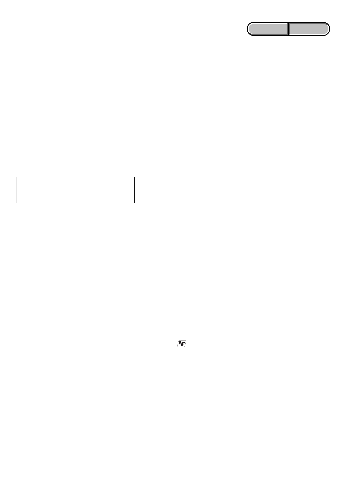
1-2. TO TAKE OUT A CASSETTE WHEN NOT EJECT (FORCE EJECT)
1 Refer to “2. DISASSEMBLY” to remove the mechanism deck block.
2 Supply +4.5 V from the DC power supply to the loading motor and unload with a pressing the cassette compartment.
Loading motor
DC power suppl
(+ 4.5 Vdc)
1-3. SETTING THE “FORCED POWER ON” MODE
It is possible to turn on power by adjustment remote commander (RM-95 or NEW LANC JIG).
Operate the VTR function using the adjustment remote commander.
1-3-1. Setting the “Forced Camera Power ON” Mode
1) Select page: 0, address: 01, and set data:01.
2) Select page: A, address: 10, set data:01 and press the “PAUSE (Write) ” button of the adjustment remote commander.
1-3-2. Setting the “Forced VTR Power ON” Mode
1) Select page: 0, address: 01, and set data:01.
2) Select page: A, address: 10, set data:02 and press the “PAUSE (Write) ” button of the adjustment remote commander.
1-3-3. Exiting the “Forced Power ON” Mode
1) Select page: 0, address: 01, and set data:01.
2) Select page: A, address: 10, set data:00 and press the “PAUSE (Write) ” button of the adjustment remote commander.
3) Select page: 0, address: 01, and set data: 00.
HDR-HC5/HC5E/HC7/HC7E_L2
1-1
Page 9
ENGLISH JAPANESE
ENGLISH JAPANESE
1-4. USING SERVICE JIG
Connect the CPC-15 jig connector (J-6082-564-A) and I/F unit for LANC control (J-6082-521 A) to the CN8103 on the US-013 board.
CPC-15
(J-6082-564-A)
FLexible Flat Cable (FFC-107)
CN8103
CN8101
8
1
8
1
CN8003
CN8001 (SIDE B)
MS-361 BOARD
(SIDE A)
VC-500 BOARD
(SIDE A)
FP-649 Flexible
CN1012
1-5. SELF-DIAGNOSIS FUNCTION
1-5-1. Self-diagnosis Function
When problems occur while the unit is operating, the self-diagnosis
function starts working, and displays on the viewfinder or LCD
screen what to do.
Details of the self-diagnosis functions are provided in the Instruction
manual.
US-013 BOARD
(SIDE A)
I/F unit for LANC control
(J-6082-521-A)
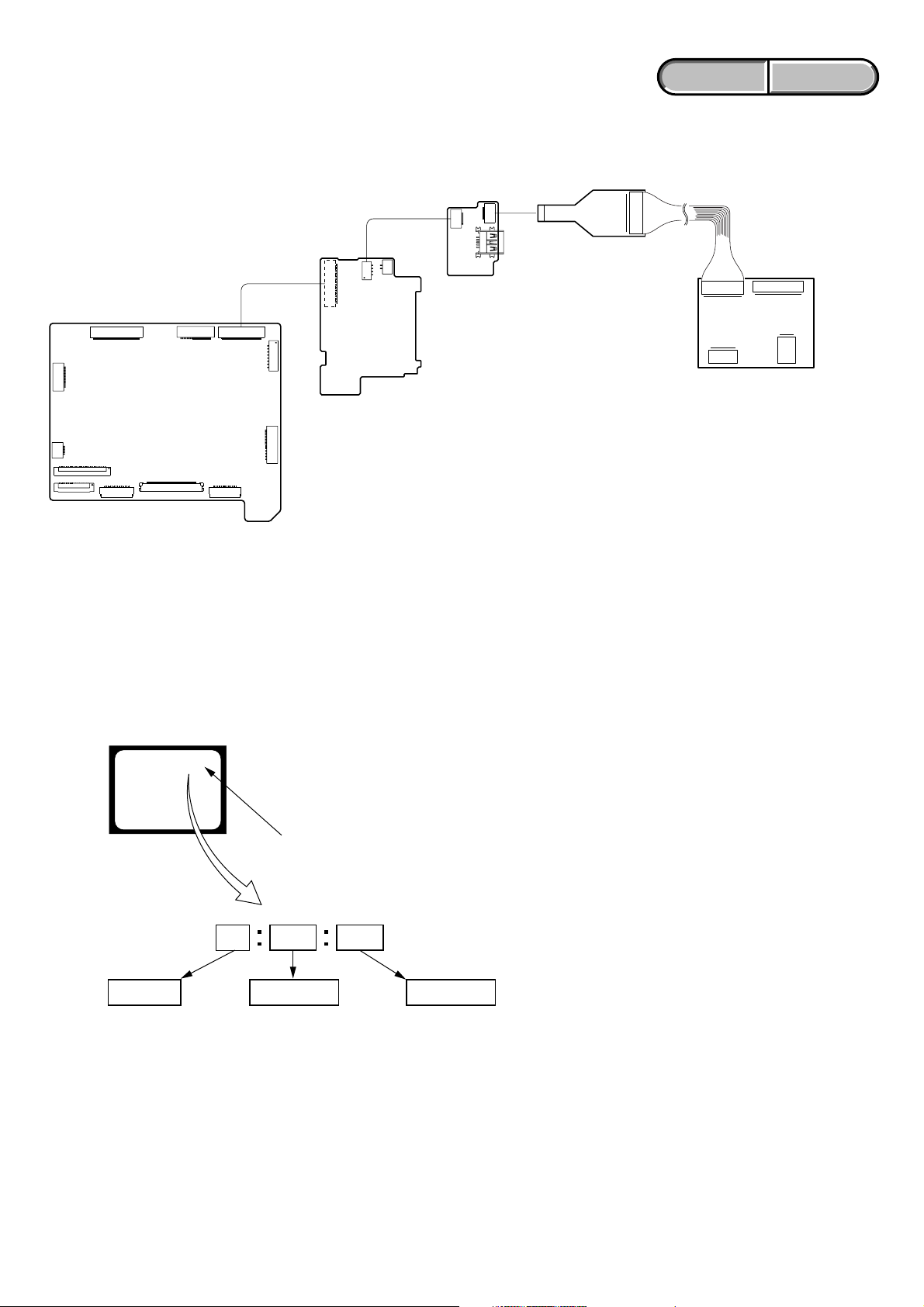
1-5-2. Self-diagnosis Display
When problems occur while the unit is operating, the counter of the
viewfinder or LCD screen shows a 4-digit display consisting of an
alphabet and numbers, which blinks at 3.2 Hz. This 5-character
display indicates the “repaired by:”, “block” in which the problem
occurred, and “detailed code” of the problem.
Viewfinder or LCD screen
C : 3 1 : 1 1
Repaired by:
C : Corrected by customer
H : Corrected by dealer
E : Corrected by service
engineer
Blinks at 3.2Hz
3 1C
1 1
Block
Indicates the appropriate
step to be taken.
E.g.
31 ....Reload the tape.
32 ....Turn on power again.
Detailed Code
Refer to 1-5-3. Self-diagnosis Code Table .
HDR-HC5/HC5E/HC7/HC7E_L2
1-2
Page 10
1-5-3. Self-diagnosis Code Table
Self-diagnosis Code
ENGLISH JAPANESE
ENGLISH JAPANESE
Block
Function
Repaired by:
C
04
C
21
C
22
C
31
C
31
C
31
C
31
C
31
C
31
C
31
C
31
C
31
C
31
C
31
C
31
C
31
C
32
C
32
C
32
C
32
C
32
C
32
C
32
C
32
C
32
C
32
C
32
C
32
C
32
C
32
Detailed
Code
00
00
00
10
11
20
21
22
23
30
31
40
41
42
43
44
10
11
20
21
22
23
30
31
40
41
42
43
44
60
Symptom/State
Non-standard battery is used.
Condensation.
Video head is dirty.
LOAD direction. Loading does not
complete within specified time
UNLOAD direction. Loading does not
complete within specified time
T reel side tape slacking when unloading
S reel
side tape slacking when unloading
T reel fault.
S reel fault.
FG fault when starting capstan.
FG fault during normal capstan operations.
FG fault when starting drum.
PG fault when starting drum.
FG fault during normal drum operations.
PG fault during normal drum operations.
Phase fault during normal drum operations.
LOAD direction loading motor time-
out.
UNLOAD direction loading motor
time-out.
T reel side tape slacking when
unloading.
S reel side tape slacking when
unloading.
T reel fault.
S reel fault.
FG fault when starting capstan.
FG fault during normal capstan
operations.
FG fault when starting drum.
PG fault when starting drum.
FG fault during normal drum
operations.
PG fault during normal drum
operations.
Phase fault during normal drum
operations.
Difficult to adjust focus.
(Cannot initialize focus.
)
Correction
Use the InfoLITHIUM battery.
Remove the cassette, and insert it again after one hour.
Clean with the optional cleaning cassette.
Load the tape again, and perform operations from the beginning.
Load the tape again, and perform operations from the beginning.
.
Load the tape again, and perform operations from the beginning.
.
Load the tape again, and perform operations from the beginning.
Load the tape again, and perform operations from the beginning.
Load the tape again, and perform operations from the beginning.
Load the tape again, and perform operations from the beginning.
Load the tape again, and perform operations from the beginning.
Load the tape again, and perform operations from the beginning.
Load the tape again, and perform operations from the beginning.
Load the tape again, and perform operations from the beginning.
Load the tape again, and perform operations from the beginning.
Load the tape again, and perform operations from the beginning.
Remove the battery or power cable, connect, and perform
operations from the beginning.
Remove the battery or power cable, connect, and perform
operations from the beginning.
Remove the battery or power cable, connect, and perform
operations from the beginning.
Remove the battery or power cable, connect, and perform
operations from the beginning.
Remove the battery or power cable, connect, and perform
operations from the beginning.
Remove the battery or power cable, connect, and perform
operations from the beginning.
Remove the battery or power cable, connect, and perform
operations from the beginning.
Remove the battery or power cable, connect, and perform
operations from the beginning.
Remove the battery or power cable, connect, and perform
operations from the beginning.
Remove the battery or power cable, connect, and perform
operations from the beginning.
Remove the battery or power cable, connect, and perform
operations from the beginning.
Remove the battery or power cable, connect, and perform
operations from the beginning.
Remove the battery or power cable, connect, and perform
operations from the beginning.
Remove the battery or power cable, connect, and perform
operations from the beginning.
If it does not recover, inspect the focus MR sensor of lens block
(Pin ql, wa of CN5302 (HC5/HC5E) or Pin qh, qk of CN5301
(HC7/HC7E) on the LD-221 board).
If not faulty, inspect the focus motor dr ive circuit
(IC5404 on the LD-221 board).
HDR-HC5/HC5E/HC7/HC7E_L2
1-3
Page 11
Self-diagnosis Code
ENGLISH JAPANESE
ENGLISH JAPANESE
Block
Function
Repaired by:
E
61
E
61
E
62
E
62
E
62
E
62
E
62
E
62
E
62
E
62
Detailed
Code
10
11
00
01
02
03
10
11
12
20
Symptom/State
Zoom operations fault.
(Cannot initialize zoom lens.)
Focus lens initializing failure and zoom
lens initializing failure occur simultaneously.
Steadyshot function does not work well.
(With pitch angular velocity sensor output
stopped.)
Steadyshot function does not work well.
(With yaw angular velocity sensor output
stopped.)
Abnormality of IC for steadyshot.
IC for steadyshot and micro controller
communication abnormality among.
Shift lens initializing failure.
Shift lens overheating (Pitch).
Shift lens overheating (Yaw).
Abnormality of thermistor.
Correction
Inspect the zoom MR sensor of lens block (Pin qh, qk of CN5302
(HC5/HC5E) or Pin w;, wa of CN5301 (HC7/HC7E) on the LD221 board) when zooming is performed when the zoom switch is
operated and the zoom motor drive circuit (IC5404 on the LD-221
board) when zooming is not performed.
Check both C: 32: 60 and E: 61: 10 of the self-diagnosis code.
Inspect pitch angular velocity sensor (SE8202 on the CM-076 board
(HC5/HC5E) or SE7202 on the CM-077 board (HC7/HC7E))
peripheral circuits.
Inspect yaw angular velocity sensor (SE8201 on the CM-076 board
(HC5/HC5E) or SE7201 on the CM-077 board (HC7/HC7E))
peripheral circuits.
Refer to [1-7-1. E : 62 : 02 (Abnormality of IC for Steadyshot)
Occurred] (HC7/HC7E only).
Inspect the steadyshot circuit (IC5703 on the LD-221 board)
(HC7/HC7E only).
Refer to [1-7-2. E : 62 : 10 (Shift Lens Initializing Failure)
Occurred] (HC7/HC7E only).
Refer to [1-7-3. E : 62 : 11 (Shift Lens Overheating (Pitch))
Occurred] (HC7/HC7E only).
Refer to [1-7-4. E : 62 : 12 (Shift Lens Overheating (Yaw))
Occurred] (HC7/HC7E only).
Refer to [1-7-5. E : 62 : 20 (Abnormality of Thermistor)
Occurred] (HC7/HC7E only).
E
91
Note: After repair, be sure to perform “1-6. PROCESS AFTER FIXING FLASH ERROR”.
01
Abnormality when flash is being charged.
Checking of flash unit or replacement of flash unit. (Note)
1-6. PROCESS AFTER FIXING FLASH ERROR
When “FLASH error” (Self-diagnosis Code E:91:**) occurs, to prevent any abnormal situation caused by high voltage, setting of the flash
is changed automatically to disabling charge and flash setting.
After fixing, this setting needs to be deactivated. Connect the adjustment remote commander (RM-95 or NEW LANC JIG) and perform the
following process.
Order Page Address Data Procedure
17 0175
27 00 01 Press PAUSE (Write) button.
37 02 Check the data changes to “01”.
HDR-HC5/HC5E/HC7/HC7E_L2
1-4
Page 12
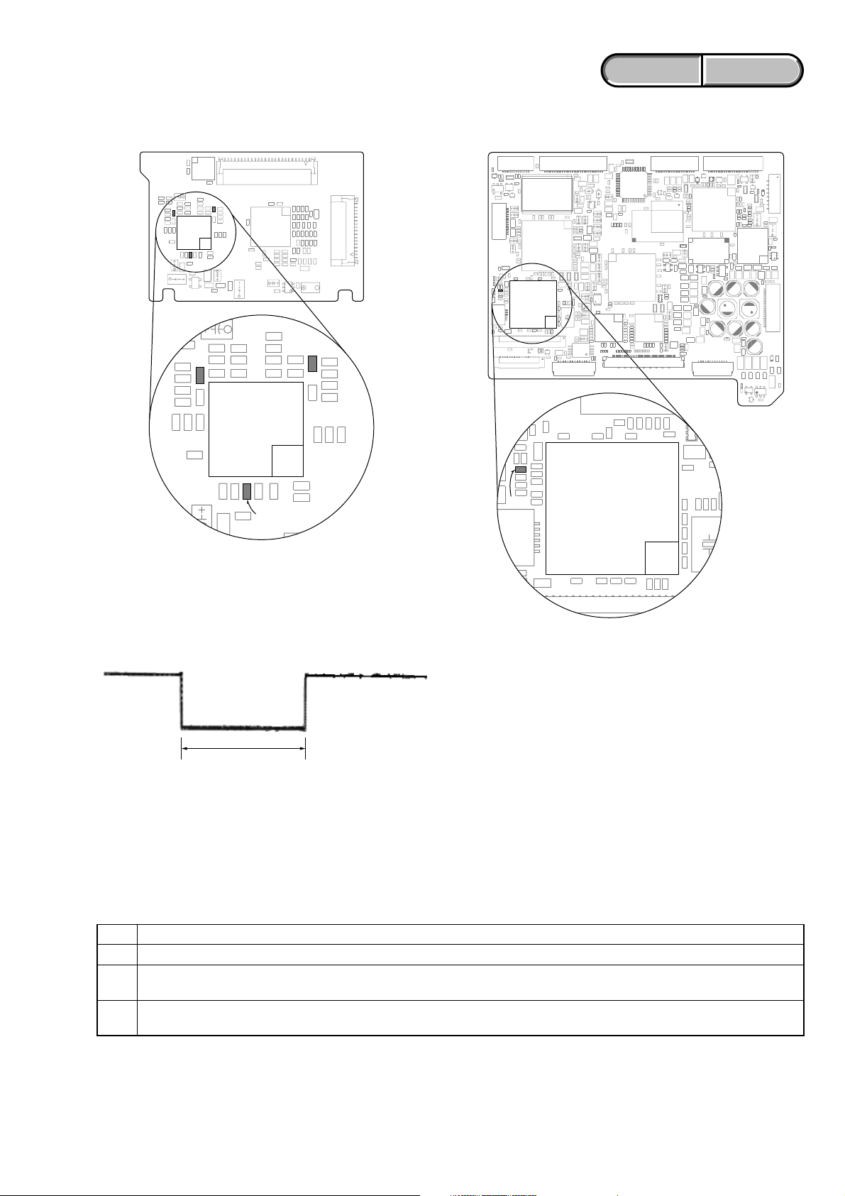
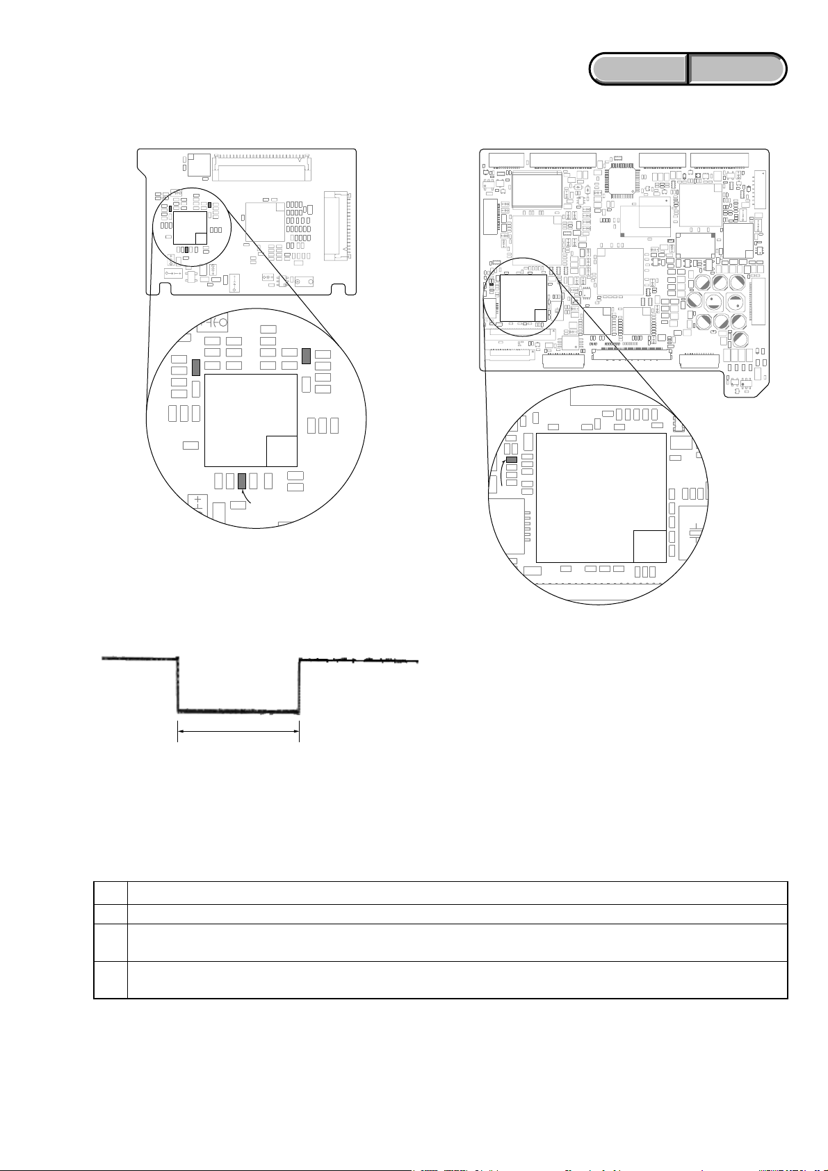
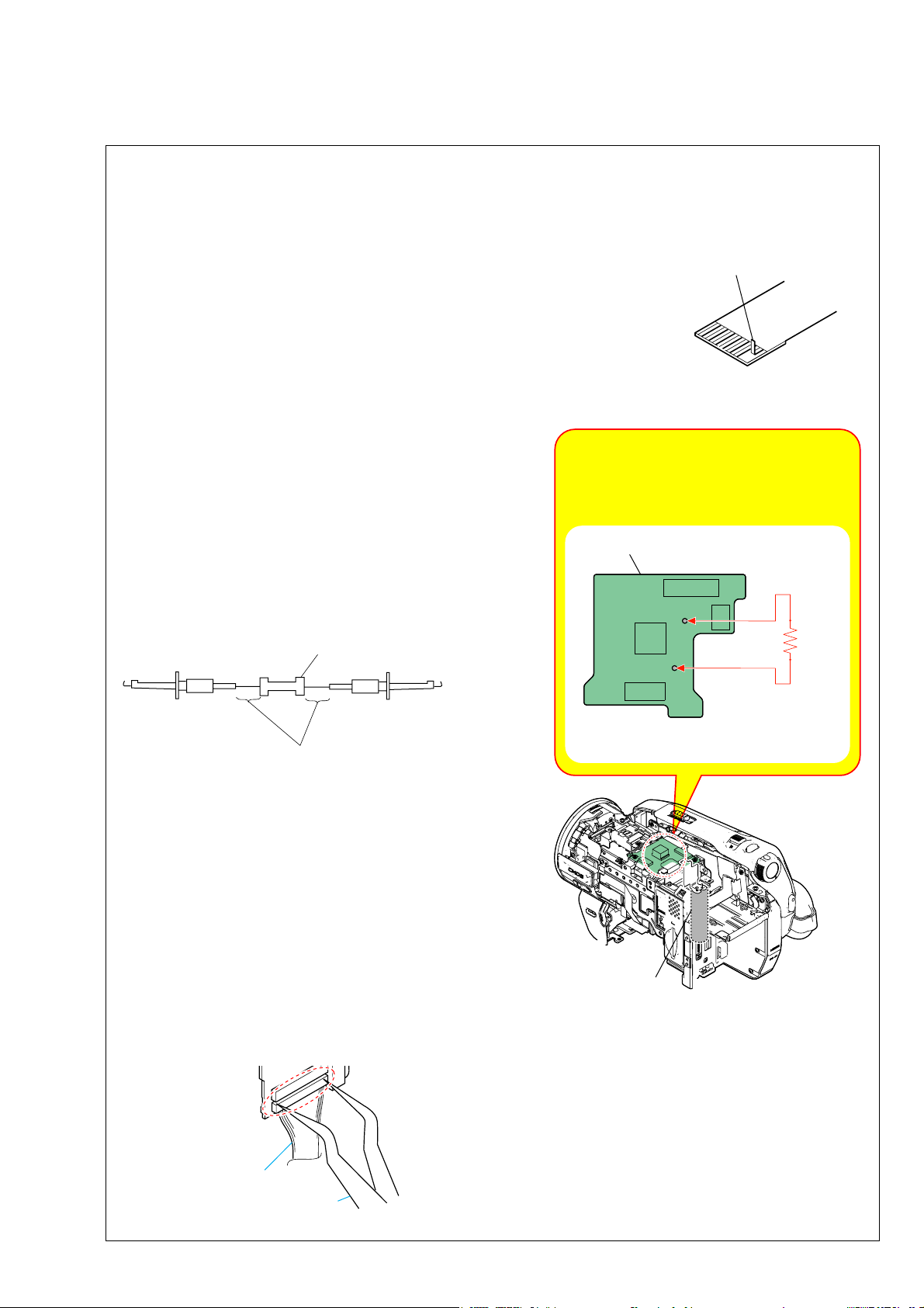
1-7. METHOD OF COPING WITH SHIFT LENS ERROR (HC7/HC7E)
IC5703
R5737
R5792
R5721
IC1801
R1823
IC1801
R1823
ENGLISH JAPANESE
ENGLISH JAPANESE
LD-221 BOARD (SIDE A)
VC-500 BOARD (SIDE A)
Fig. 1
Measurement points on the LD-221 board
Fig. 3
Measurement points on the VC-500 board
about 330 msec
Note: The length of low section will vary a little depending on the
conditions.
Fig. 2
Change in output voltage of R5792 on the LD-221 board
1-7-1. E : 62 : 02 [Abnormality of IC for Steadyshot] Occurred
Order Procedure
1Turn the power OFF.
While measuring with an oscilloscope the output voltage of R5792 in the periphery of IC5703 on the LD-221 board, turn the
2
power ON to check that the output voltage immediately after the power on change as shown in Fig. 2.
If the output voltage change as shown in Fig. 2, replace the lens block (Note). If it does not change as shown in Fig. 2, inspect
3
the camera control circuit (IC1801 of VC-500 board) periphery.
Note: When the lens block was replaced, execute a necessary adjustment items referring to Service Manual, ADJ.
After the adjustment, make sure with the STEADYSHOT turned ON that the steadyshot functions appropriately in the
handheld operation.
HDR-HC5/HC5E/HC7/HC7E_L2
1-5
Page 13
1-7-2. E : 62 : 10 [Shift Lens Initializing Failure] Occurred
Connect the adjustment remote commander (RM-95 or NEW LANC JIG) and perform the following process.
Order Page Address Data Procedure
10 0101
20 1007
F
3
(7F)
F
4
(7F)
F
5
(7F)
06 Read the data value and assume it as D
06
06 D
Change the data and check that it has been changed. If no value changes or if value is 00 or FF, inspect
the EEPROM (IC1802 of VC-500 board). If value changes, proceed to the order 5.
06 Press PAUSE (Write) button.
06.
ENGLISH JAPANESE
ENGLISH JAPANESE
F
6
(7F)
F
7
(7F)
F
8
(7F)
07 Read the data value and assume it as D
07
07 D
Change the data and check that it has been changed. If no value changes or if value is 00 or FF, inspect
the EEPROM (IC1802 of VC-500 board). If value changes, proceed to the order 8.
07 Press PAUSE (Write) button.
07.
90 1000
10 0 01 00
Perform “Hall Adjustment”. (Note 1)
11 If the lens does not move at all when adjusting it, proceed to the order 12. When the adjustment ends,
proceed to the order 16. (Note 1)
12 2 01 2D Press PAUSE (Write) button.
13 2 02
Read the data value. If value is not 01, inspect the EEPROM (IC1802 of VC-500 board). When value
is 01, proceed to the order 14.
14 2 01 00 Press PAUSE (Write) button.
15 Turn the power OFF and ON again.
16 Check that no error occurs. If an error occurs, replace the lens block (Note 2).
Note 1: Perform adjustment by referring to “Hall Adjustment” in Service Manual, ADJ. After the adjustment, be sure to perf orm
“Angular Velocity Sensor Sensitivity Adjustment”.
Note 2: When the lens block was replaced, execute the necessary adjustment items referring to Service Manual, ADJ.
After the adjustment, make sure with the STEADYSHOT turned ON that the steadyshot functions appropriately in the
handheld operation.
HDR-HC5/HC5E/HC7/HC7E_L2
1-6
Page 14
ENGLISH JAPANESE
ENGLISH JAPANESE
1-7-3. E : 62 : 11 [Shift Lens Overheating (Pitch)] Occurred
Connect the adjustment remote commander (RM-95 or NEW LANC JIG) and perform the following process.
Order Page Address Data Procedure
10 0101
20 1006
B
3
(6B)
40 1007
D
5
(7D)
D
6
(7D)
D
7
(7D)
D
8
(7D)
D
9
(7D)
D
10
(7D)
11 0 10 06
B
12
(6B)
13 0 10 00
14 0 01 00
15
16
17
18 Turn the power OFF.
19
20
B2 01 Press PAUSE (Write) button.
46 F0 Press PAUSE (Write) button.
48 01 Press PAUSE (Write) button. (Note 1)
48 00 Press PAUSE (Write) button.
46 10 Press PAUSE (Write) button.
48 01 Press PAUSE (Write) button. (Note 1)
48 00 Press PAUSE (Write) button.
B2 00 Press PAUSE (Write) button.
Check if the shift lens moves while setting the order 5 to 10. If the shift lens does not move, replace the
lens block (Note 2). When the shift lens moved, proceed to the order 16.
While setting the order 5 to 10, measure with an oscilloscope the output voltage of R5721 in the periphery
of IC5703 on the LD-221 board to check the output voltage varies.
If the output voltage does not vary, replace the lens block (Note 2). When the output voltage varied,
proceed to the order 18.
While measuring with an oscilloscope the output voltage of R5792 in the periphery of IC5703 on the
LD-221 board, turn the power ON to check that the output voltage immediately after the power on
change as shown in Fig. 2.
If the output voltage change as shown in Fig. 2, replace the lens block (Note 2). If it does not change as
shown in Fig. 2, inspect the camera control circuit (IC1801 of VC-500 board) periphery.
Note 1: Finish this operation within 10 seconds. If it is likely to take more than 10 seconds, set page: D (7D), address: 48, data:
00, and then retry.
Note 2: When the lens block was replaced, execute the necessary adjustment items referring to Service Manual, ADJ.
After the adjustment, make sure with the STEADYSHOT turned ON that the steadyshot functions appropriately in the
handheld operation.
HDR-HC5/HC5E/HC7/HC7E_L2
1-7
Page 15
1-7-4. E : 62 : 12 [Shift Lens Overheating (Yaw)] Occurred
Connect the adjustment remote commander (RM-95 or NEW LANC JIG) and perform the following process.
Order Page Address Data Procedure
10 0101
20 1006
B
3
(6B)
40 1007
D
5
(7D)
D
6
(7D)
D
7
(7D)
D
8
(7D)
D
9
(7D)
D
10
(7D)
11 0 10 06
B
12
(6B)
13 0 10 00
14 0 01 00
15
16
17
18 Turn the power OFF.
19
20
B2 01 Press PAUSE (Write) button.
47 F0 Press PAUSE (Write) button.
49 01 Press PAUSE (Write) button. (Note 1)
49 00 Press PAUSE (Write) button.
47 10 Press PAUSE (Write) button.
49 01 Press PAUSE (Write) button. (Note 1)
49 00 Press PAUSE (Write) button.
B2 00 Press PAUSE (Write) button.
Check if the shift lens moves while setting the order 5 to 10. If the shift lens does not move, replace the
lens block (Note 2). When the shift lens moved, proceed to the order 16.
While setting the order 5 to 10, measure with an oscilloscope the output voltage of R5737 in the periphery
of IC5703 on the LD-221 board to check the output voltage varies.
If the output voltage does not vary, replace the lens block (Note 2). When the output voltage varied,
proceed to the order 18.
While measuring with an oscilloscope the output voltage of R5792 in the periphery of IC5703 on the
LD-221 board, turn the power ON to check that the output voltage immediately after the power on
change as shown in Fig. 2.
If the output voltage change as shown in Fig. 2, replace the lens block (Note 2). If it does not change as
shown in Fig. 2, inspect the camera control circuit (IC1801 of VC-500 board) periphery.
ENGLISH JAPANESE
ENGLISH JAPANESE
Note 1: Finish this operation within 10 seconds. If it is likely to take more than 10 seconds, set page: D (7D), address: 49, data:
00, and then retry.
Note 2: When the lens block was replaced, execute the necessary adjustment items referring to Service Manual, ADJ.
After the adjustment, make sure with the STEADYSHOT turned ON that the steadyshot functions appropriately in the
handheld operation.
1-7-5. E : 62 : 20 [Abnormality of Thermistor] Occurred
Order Procedure
1Turn the power ON.
Check that R1823 in the periphery of IC1801 on the VC-500 board is 0 Ω and energizes. If it is not energizes, replace the R1823.
2
When R1823 is 0 Ω and energizes, replace the lens block (Note).
Check that no error occurs, after replacing the lens block and performing the necessary adjustment. If an error occurs, inspect
3
the camera control circuit (IC1801 of VC-500 board) periphery.
Note: When the lens block was replaced, execute the necessary adjustment items referring to Service Manual, ADJ.
After the adjustment, make sure with the STEADYSHOT turned ON that the steadyshot functions appropriately in the
handheld operation.
HDR-HC5/HC5E/HC7/HC7E_L2
1-8
Page 16
ENGLISH JAPANESE
1. SERVICE NOTE
ENGLISH JAPANESE
1-1. 修理時の電源供給について
本機では,安定化電源(8.4Vdc)からバッテリ端子に電源を供給した場合,約10秒後にシャットオフし,動作しなくなります。
これを避けるため,下記の方法を用いてください。
方法:
DC入力端子を使用する。(ACアダプタ(AC-L200/L200B)を使用する。)
1-2. イジェクトしない時のカセット取出し方法(強制イジェクト)
1 2.DISASSEMBLYを参照し,メカデッキを外す。
2 カセコン組立を押さえながら,安定化電源より+4.5Vをローディングモータに加え,アンローディングさせる。
ローディングモータ
安定化電源(+4.5Vdc)
1-3. 強制電源ONモードの設定
調整リモコン(RM-95またはNEWLANCJIG)を使用して,電源を入れることが出来ます。
VTR操作は調整リモコンで行えます。
1-3-1. 強制カメラ電源ONモードの設定
1) ページ:0,アドレス:01にデータ:01をセット。
2) ページ:A,アドレス:10にデータ:01をセットしPAUSE(Write)ボタンを押す。
1-3-2. 強制VTR電源ONモードの設定
1) ページ:0,アドレス:01にデータ:01をセット。
2) ページ:A,アドレス:10にデータ:02をセットしPAUSE(Write)ボタンを押す。
1-3-3. 強制電源ONモードの解除
1) ページ:0,アドレス:01にデータ:01をセット。
2) ページ:A,アドレス:10にデータ:00をセットしPAUSE(Write)ボタンを押す。
3) ページ:0,アドレス:01にデータ:00をセット。
HDR-HC5/HC5E/HC7/HC7E_L2
1-9
Page 17
ENGLISH JAPANESE
ENGLISH JAPANESE
1-4. 使用サービス治具
CPC-15治具コネクタ(J-6082-564-A),LANC変換用I/F(J-6082-521-A)をUS-013基板CN8103に接続します。
CPC-15
(J-6082-564-A)
FLexible Flat Cable (FFC-107)
CN8103
CN8101
8
1
8
1
CN8003
CN8001 (SIDE B)
MS-361 BOARD
(SIDE A)
VC-500 BOARD
(SIDE A)
FP-649 Flexible
CN1012
1-5. 自己診断機能
1-5-1.自己診断機能について
本機の動作に不具合が生じたとき,自己診断機能が働き,
ビューファインダまたはLC D 画面に,どう処置したらよい
か判断できる表示を行います。自己診断機能については取扱
説明書にも掲載されています。
US-013 BOARD
(SIDE A)
I/F unit for LANC control
(J-6082-521-A)
1-5-2.自己診断表示
本機の動作に不具合が生じたとき,ビューファインダまたは
LCD画面のカウンタ表示部分がアルファベットと数字の4桁
表示になり,3.2Hzで点滅します。この5文字の表示によっ
て対応者分類および不具合の生じたブロックの分類,不具合
の詳細コードを示します。
ビューファインダまたはLCD画面
C : 3 1 : 1 1
対応者分類
C :お客さま自身で対応
H :販売店で対応
E :サービスエンジニア
対応方法の違いにより分類
例 31・・・テープを入れ直す
32・・・電源を入れ直す
で対応
3.2Hz点滅
3 1C
ブロック分類
1 1
詳細コード
「1-5-3.自己診断コード表」
を参照
HDR-HC5/HC5E/HC7/HC7E_L2
1-10
Page 18
1-5-3.自己診断コード表
自己診断コード
対
応
者
C
C
C
C
C
C
C
C
C
C
C
C
C
C
C
C
C
C
C
C
C
C
C
C
C
C
C
C
C
C
ブロック
機能
04
21
22
31
31
31
31
31
31
31
31
31
31
31
31
31
32
32
32
32
32
32
32
32
32
32
32
32
32
32
詳細
コード
00
00
00
10
11
20
21
22
23
30
31
40
41
42
43
44
10
11
20
21
22
23
30
31
40
41
42
43
44
60
症状/状態
標準でないバッテリを使用している
結露している
ビデオヘッドが汚れている
LOAD方向,ローディング所定時間
内終了せず
UNLOAD方向,ローディング所定
時間内終了せず
UNLOAD時,Tリール側テープ弛み
UNLOAD時,Sリール側テープ弛み
Tリール異常
Sリール異常
キャプスタン起動時FG異常
キャプスタン定常時FG異常
ドラム起動時FG異常
ドラム起動時PG異常
ドラム定常時FG異常
ドラム定常時PG異常
ドラム定常時位相異常
LOAD方向,ローディング所定時間
内終了せず
UNLOAD方向,ローディング所定
時間内終了せず
UNLOAD時,Tリール側テープ弛み
UNLOAD時,Sリール側テープ弛み
Tリール異常
Sリール異常
キャプスタン起動時FG異常
キャプスタン定常時FG異常
ドラム起動時FG異常
ドラム起動時PG異常
ドラム定常時FG異常
ドラム定常時PG異常
ドラム定常時位相異常
フォーカスが合いにくい
(フォーカスの初期化ができない)
ENGLISH JAPANESE
ENGLISH JAPANESE
対応/方法
インフォリチウムバッテリを使用する。
カセットを取り出して,約1時間してからもう一度入れ直す。
別売のクリーニングカセットできれいにする。
テープを入れ直し,再度操作し直す。
テープを入れ直し,再度操作し直す。
テープを入れ直し,再度操作し直す。
テープを入れ直し,再度操作し直す。
テープを入れ直し,再度操作し直す。
テープを入れ直し,再度操作し直す。
テープを入れ直し,再度操作し直す。
テープを入れ直し,再度操作し直す。
テープを入れ直し,再度操作し直す。
テープを入れ直し,再度操作し直す。
テープを入れ直し,再度操作し直す。
テープを入れ直し,再度操作し直す。
テープを入れ直し,再度操作し直す。
バッテリまたは電源ケーブルを外して付け直し,再度操作し直す。
バッテリまたは電源ケーブルを外して付け直し,再度操作し直す。
バッテリまたは電源ケーブルを外して付け直し,再度操作し直す。
バッテリまたは電源ケーブルを外して付け直し,再度操作し直す。
バッテリまたは電源ケーブルを外して付け直し,再度操作し直す。
バッテリまたは電源ケーブルを外して付け直し,再度操作し直す。
バッテリまたは電源ケーブルを外して付け直し,再度操作し直す。
バッテリまたは電源ケーブルを外して付け直し,再度操作し直す。
バッテリまたは電源ケーブルを外して付け直し,再度操作し直す。
バッテリまたは電源ケーブルを外して付け直し,再度操作し直す。
バッテリまたは電源ケーブルを外して付け直し,再度操作し直す。
バッテリまたは電源ケーブルを外して付け直し,再度操作し直す。
バッテリまたは電源ケーブルを外して付け直し,再度操作し直す。
バッテリまたは電源ケーブルを外して付け直し,再度操作し直す。
復帰しない場合,レンズブロックのフォーカス MR センサ
(LD-221基板CN5302ql,waピ ン(HC5/HC5E)またはCN5301
qh,qkピン(HC7/HC7E))を点検。問題がなければフォーカス
モータドライブ回路(LD-221基板IC5404)を点検。
HDR-HC5/HC5E/HC7/HC7E_L2
1-11
Page 19
自己診断コード
対
ブロック
応
機能
者
E
61
詳細
コード
10
症状/状態
ズーム動作の異常(ズームレンズの
初期化ができない)
ENGLISH JAPANESE
ENGLISH JAPANESE
対応/方法
ズームレバーを操作した時,ズーム動作をすればレンズブ
ロックのズームMRセンサ(LD-221基板CN5302qh,qkピン
(HC5/HC5E)またはCN5301w;,waピン(HC7/HC7E))を点検。
ズーム動作をしなければズームモータドライブ回路(LD-221
基板IC5404)を点検。
E
E
E
E
E
E
E
E
E
E
61
62
62
62
62
62
62
62
62
91
11
00
01
02
03
10
11
12
20
01
(PITCH角速度センサ出力張り付き)
(YAW角速度センサ出力張り付き)
フォーカスレンズ初期化異常,ズー
ムレンズ初期化異常の同時発生
手振れ補正が効きにくい
手振れ補正が効きにくい
手振れ補正用ICの異常
手振れ補正用ICとマイクロコント
ローラーとの通信異常
シフトレンズ初期化異常
シフトレンズオーバーヒート
(PITCH)
シフトレンズオーバーヒート
(YAW)
サーミスタの異常
フラッシュの充電異常
自己診断コードC:32:60とE:61:10の両方を点検。
PITCH角速度センサ(CM-076基板SE8202(HC5/HC5E)また
はCM-077基板SE7202(HC7/HC7E))周辺回路を点検。
YAW角速度センサ(CM-076基板SE8201(HC5/HC5E)または
CM-077基板SE7201(HC7/HC7E))周辺回路を点検。
「1-7-1.E:62:02(手振れ補正用ICの異常)が出た場合」を参照。
(HC7/HC7Eのみ)
手振れ補正回路(LD-221基板IC5703)を点検。
(HC7/HC7Eのみ)
「1-7-2.E:62:10(シフトレンズ初期化異常)が出た場合」を参照。
(HC7/HC7Eのみ)
「1-7-3.E:62:11(シフトレンズオーバーヒート(PITCH))が出
た場合」を参照。(HC7/HC7Eのみ)
「1-7-4.E:62:12(シフトレンズオーバーヒート(YAW))が出
た場合」を参照。(HC7/HC7Eのみ)
「1-7-5.E:62:20(サーミスタの異常)が出た場合」を参照。
(HC7/HC7Eのみ)
フラッシュユニットの点検または交換(注)
注意:修理後は,必ず「1-6.フラッシュ異常修理後の処置」を行ってください。
1-6. フラッシュ異常修理後の処置
フラッシュエラー(自己診断コードE:91:**)発生時は、高電圧による異常を防止するために自動的にフラッシュ充電・
発光禁止の設定になります。修理後は、この設定を解除する必要があります。調整用リモコン(RM-95またはNEWLANC
JIG)を接続し、下記の処置を行ってください。
順序 ページ アドレスデータ 作業内容
17 0175
27 00 01 PAUSE(Write)ボタンを押す
37 02 データが01になることを確認
HDR-HC5/HC5E/HC7/HC7E_L2
1-12
Page 20
1-7. シフトレンズエラーの対処方法(HC7/HC7E)
IC5703
R5737
R5792
R5721
IC1801
R1823
IC1801
R1823
ENGLISH JAPANESE
ENGLISH JAPANESE
LD-221 BOARD (SIDE A)
VC-500 BOARD (SIDE A)
図1.LD-221基板測定箇所
図3.VC-500基板測定箇所
約330msec
注意:Lowの区間の長さは場合によって多少異なる
図2.LD-221基板R5792の出力電圧の変化
1-7-1. E:62:02(手振れ補正用ICの異常)が出た場合
順序 作業内容
1 電源を切る。
LD-221基板IC5703の周辺にあるR5792の出力電圧をオシロスコープで測定しながら電源を入れる。電源投入直後の
2
出力電圧が図2の様に変化することを確認する。
出力電圧が図2の様に変化するときはレンズブロックを交換する(注)。図2の様に変化しないときはカメラコント
3
ロール回路(VC-500基板IC1801)周辺を点検する。
注意: レンズブロックを交換した場合は,A D J 編を参照して必要な調整項目を実施すること。調整後は手振れ補正O N の状
態にして,手持ち動作で手振れ補正が適切に動作していることを確認する。
HDR-HC5/HC5E/HC7/HC7E_L2
1-13
Page 21
1-7-2. E:62:10(シフトレンズ初期化異常)が出た場合
調整用リモコン(RM-95またはNEWLANCJIG)を接続し、次の手順を行う。
順序 ページ アドレスデータ 作業内容
10 0101
20 1007
F
3
(7F)
F
4
(7F)
F
5
(7F)
F
6
(7F)
F
7
(7F)
F
8
(7F)
06 データ値を読み取り,その値をD
06
06 D
データを変更し値が変わることを確認する。値が変化しない,もしくは値が00またはFFに
なっている場合はEEPROM(VC-500基板IC1802)を点検。値が変化する場合は順序5に進む。
06 PAUSE(Write)ボタンを押す。
07 データ値を読み取り,その値をD
07
07 D
データを変更し値が変わることを確認する。値が変化しない,もしくは値が00またはFFに
なっている場合はEEPROM(VC-500基板IC1802)を点検。値が変化する場合は順序8に進む。
07 PAUSE(Write)ボタンを押す。
06とする。
07とする。
90 1000
10 0 01 00
11
ホール調整を行う(注1)。
調整時にレンズが全く動かない場合は順序12に進む。調整が終了したら順序16に進む。(注1)
12 2 01 2D PAUSE(Write)ボタンを押す。
13 2 02
データ値が01以外になっている場合はEEPROM(VC-500基板IC1802)を点検。値が01の場合は
順序14に進む。
14 2 01 00 PAUSE(Write)ボタンを押す。
15 電源を切り,再び電源を入れる。
16
エラーが発生しないことを確認する。もしエラーが発生する場合はレンズブロックを交換
する(注2)。
ENGLISH JAPANESE
ENGLISH JAPANESE
注意1:ADJ編「HallAdjustment」を参照して調整を実施すること。調整後は「AngularVelocitySensorSensitivityAdjustment」
を必ず実施すること。
注意2:レンズブロックを交換した場合は,A D J 編を参照して必要な調整項目を実施すること。調整後は手振れ補正ONの状
態にして,手持ち動作で手振れ補正が適切に動作していることを確認する。
HDR-HC5/HC5E/HC7/HC7E_L2
1-14
Page 22
1-7-3. E:62:11(シフトレンズオーバーヒート(PITCH))が出た場合
調整用リモコン(RM-95またはNEWLANCJIG)を接続し、次の手順を行う。
順序 ページ アドレスデータ 作業内容
10 0101
20 1006
B
3
(6B)
40 1007
D
5
(7D)
D
6
(7D)
D
7
(7D)
D
8
(7D)
D
9
(7D)
D
10
(7D)
11 0 10 06
B
12
(6B)
13 0 10 00
14 0 01 00
15
16
17
18 電源を切る。
19
20
B2 01 PAUSE(Write)ボタンを押す。
46 F0 PAUSE(Write)ボタンを押す。
48 01 PAUSE(Write)ボタンを押す。(注1)
48 00 PAUSE(Write)ボタンを押す。
46 10 PAUSE(Write)ボタンを押す。
48 01 PAUSE(Write)ボタンを押す。(注1)
48 00 PAUSE(Write)ボタンを押す。
B2 00 PAUSE(Write)ボタンを押す。
順序5〜10を設定している間にシフトレンズが動いたか確認する。もしシフトレンズが動か
ない場合はレンズブロックを交換する(注2)。動く場合は順序16に進む。
LD-221基板IC5703の周辺にあるR5721の出力電圧をオシロスコープで測定しながら,順序5
〜10を設定したときに出力電圧が変化することを確認する。
出力電圧が変化しないときはレンズブロックを交換する(注2)。変化するときは順序18に進む。
LD-221基板IC5703の周辺にあるR5792の出力電圧をオシロスコープで測定しながら電源を入
れる。電源投入直後の出力電圧が図2の様に変化することを確認する。
出力電圧が図2の様に変化するときはレンズブロックを交換する(注2)。図2の様に変化しな
いときはカメラコントロール回路(VC-500基板IC1801)周辺を点検する。
ENGLISH JAPANESE
ENGLISH JAPANESE
注意1:この操作は1 0秒以内に終了してください。もし10 秒以上経過しそうな場合は,ページ:D (7D),アドレス:4 8 ,
データ:00に設定しなおしてから再度実行してください。
注意2:レンズブロックを交換した場合は,A D J編を参照して必要な調整項目を実施すること。調整後は手振れ補正ONの状
態にして,手持ち動作で手振れ補正が適切に動作していることを確認する。
HDR-HC5/HC5E/HC7/HC7E_L2
1-15
Page 23
1-7-4. E:62:12(シフトレンズオーバーヒート(YAW))が出た場合
調整用リモコン(RM-95またはNEWLANCJIG)を接続し、次の手順を行う。
順序 ページ アドレスデータ 作業内容
10 0101
20 1006
B
3
(6B)
40 1007
D
5
(7D)
D
6
(7D)
D
7
(7D)
D
8
(7D)
D
9
(7D)
D
10
(7D)
11 0 10 06
B
12
(6B)
13 0 10 00
14 0 01 00
15
16
17
18 電源を切る。
19
20
B2 01 PAUSE(Write)ボタンを押す。
47 F0 PAUSE(Write)ボタンを押す。
49 01 PAUSE(Write)ボタンを押す。(注1)
49 00 PAUSE(Write)ボタンを押す。
47 10 PAUSE(Write)ボタンを押す。
49 01 PAUSE(Write)ボタンを押す。(注1)
49 00 PAUSE(Write)ボタンを押す。
B2 00 PAUSE(Write)ボタンを押す。
順序5〜10を設定している間にシフトレンズが動いたか確認する。もしシフトレンズが動か
ない場合はレンズブロックを交換する(注2)。動く場合は順序16に進む。
LD-221基板IC5703の周辺にあるR5737の出力電圧をオシロスコープで測定しながら,順序5
〜10を設定したときに出力電圧が変化することを確認する。
出力電圧が変化しないときはレンズブロックを交換する(注2)。変化するときは順序18に進む。
LD-221基板IC5703の周辺にあるR5792の出力電圧をオシロスコープで測定しながら電源を入
れる。電源投入直後の出力電圧が図2の様に変化することを確認する。
出力電圧が図2の様に変化するときはレンズブロックを交換する(注2)。図2の様に変化しな
いときはカメラコントロール回路(VC-500基板IC1801)周辺を点検する。
ENGLISH JAPANESE
ENGLISH JAPANESE
注意1:この操作は1 0秒以内に終了してください。もし10 秒以上経過しそうな場合は,ページ:D (7D),アドレス:4 9 ,
データ:00に設定しなおしてから再度実行してください。
注意2:レンズブロックを交換した場合は,A D J編を参照して必要な調整項目を実施すること。調整後は手振れ補正ONの状
態にして,手持ち動作で手振れ補正が適切に動作していることを確認する。
1-7-5. E:62:20(サーミスタの異常)が出た場合
順序 作業内容
1 電源を入れる。
VC-500基板IC1801の周辺にあるR1823が0 Ωであり,かつ通電していることを確認する。通電していない場合は
2
R1823を交換する。R1823が0 Ωであり,かつ通電している場合は
レンズブロックを交換し必要な調整を行った後,エラーが発生しないことを確認する。もしエラーが発生する場
3
合はカメラコントロール回路(VC-500基板IC1801)周辺を点検する。
注意: レンズブロックを交換した場合は,A D J 編を参照して必要な調整項目を実施すること。調整後は手振れ補正O N の状
態にして,手持ち動作で手振れ補正が適切に動作していることを確認する。
レンズブロックを交換する(注)。
HDR-HC5/HC5E/HC7/HC7E_L2
1-16E
Page 24
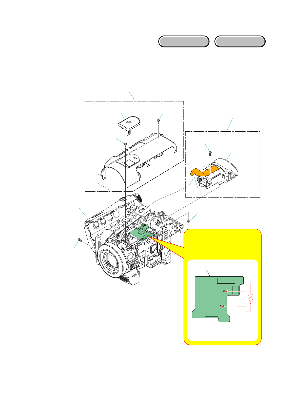
NOTE FOR REPAIR
2. DISASSEMBLY
• Make sure that the flat cable and flexible board are not cracked of bent at the terminal.
Do not insert the cable insufficiently nor crookedly.
• When remove a connector, don’t pull at wire of connector. It is possible that a wire is snapped.
• When installing a connector, don’t press down at wire of connector.
It is possible that a wire is snapped.
Cut and remove the part of gilt
which comes off at the point.
(Be careful or some
pieces of gilt may be left inside)
DISCHARGING OF THE ST-164 BOARD’S CHARGING CAPACITOR (C901)
The charging capacitor (C901) of the ST-164 board is charged
up to the maximum 330 V potential.
There is a danger of electric shock by this high voltage when the
capacitor is handled by hand. The electric shock is caused by
the charged voltage which is kept without discharging when the
main power of the unit is simply turned off. Therefore, the
remaining voltage must be discharged as described below.
Preparing the Short Jig
To preparing the short jig, a small clip is attached to each end of
a resistor of 1 kΩ /1 W (1-215-869-11).
Wrap insulating tape fully around the leads of the resistor to
prevent electrical shock.
1 kΩ/1 W
Note: High-voltage cautions
Discharging the Capacitor
Short-circuit between the two points
with the short jig about 10 seconds.
ST-164 Board
Wrap insulating tape.
C901
NOTE FOR DISCONNECTING THE HARNESS (HN-045/HN-046)
When disconnecting the harness (HN-045/HN-046), do not pull
the harness part but pull off the connector body with tweezers
etc.
Harness
(HN-045/HN-046)
R:1 kΩ/1 W
(Part code: 1-215-869-11)
HDR-HC5/HC5E/HC7/HC7E_L2
Tweezers etc.
2-1
Page 25
HELP
EXPLODED VIEW
HELP
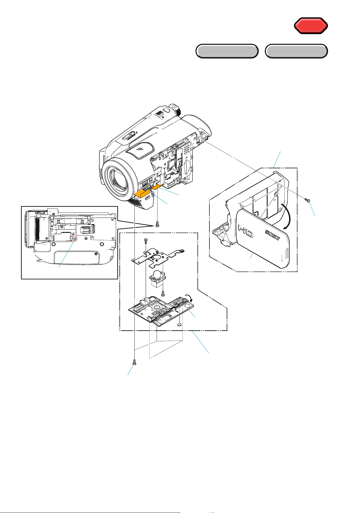
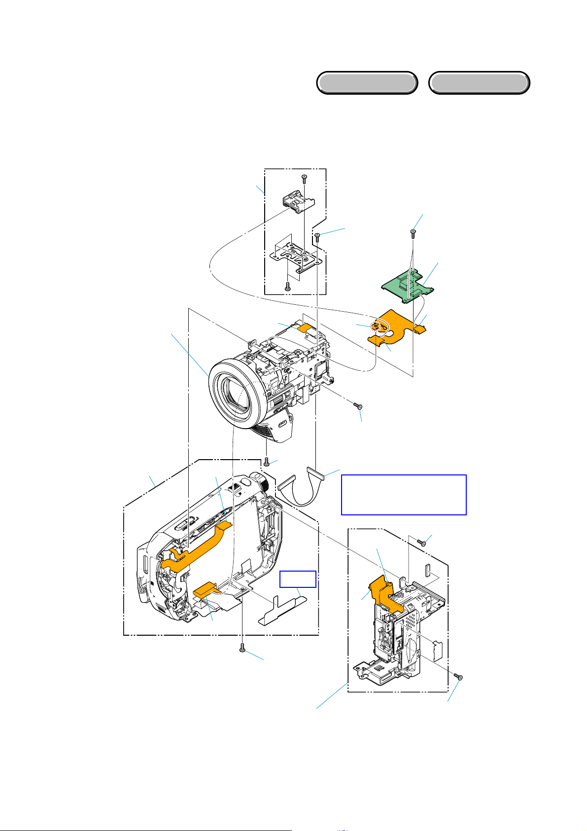
2-1. DISASSEMBLY
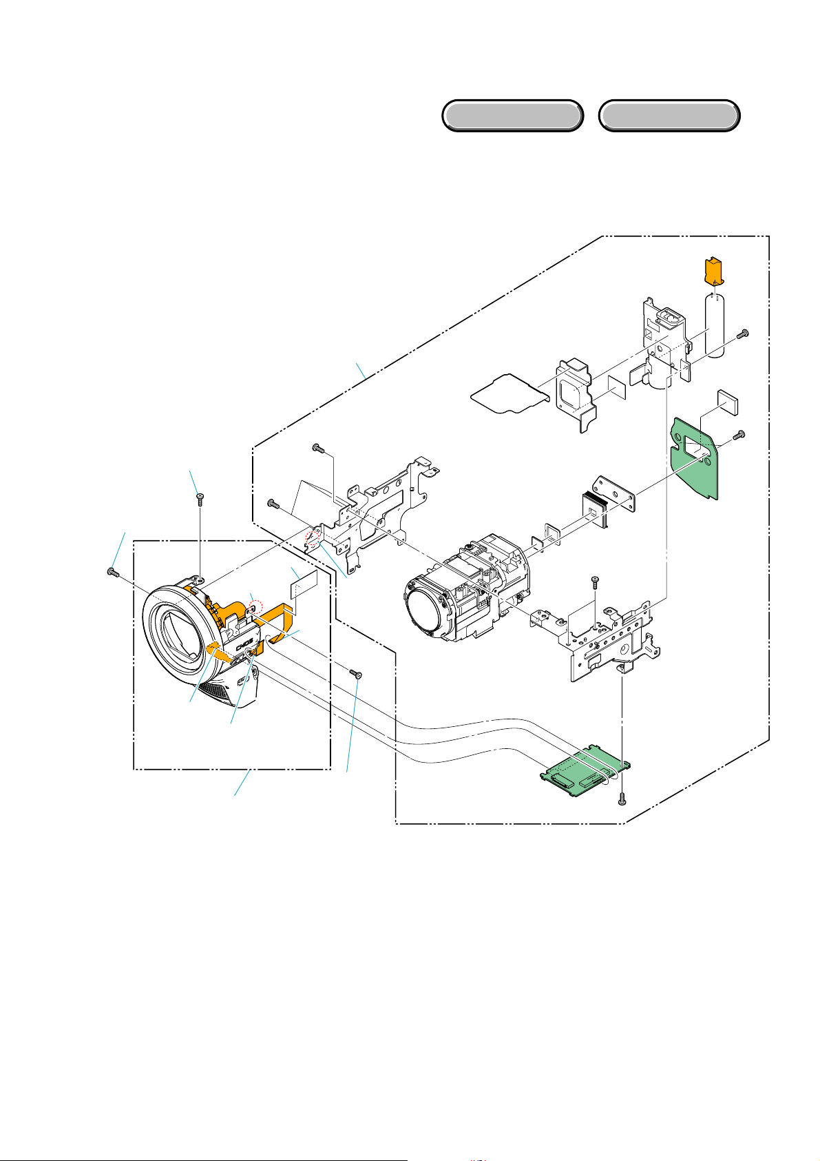
2-1-1. OVERALL SECTION
Follow the disassembly in the numerical order given.
1 Bottom Cabinet Assy (1-1 to 1-2)
2 Cabinet (R) Block (2-1 to 2-5)
HARDWARE LIST
2 Cabinet (R) Block
2-5
2-1
2-4
(#1)
2-2 (#1)
2-3
(Open)
1-2 (Open)
1 Bottom Cabinet Assy
1-1 (#2)
HDR-HC5/HC5E/HC7/HC7E_L2
2-2
Page 26
2-1-2. TOP CABINET SECTION
EXPLODED VIEW
Follow the disassembly in the numerical order given.
1 Top Cabinet Block (1-1 to 1-6)
2 VF Block Assy (2-1 to 2-3)
1 Top Cabinet Block
HARDWARE LIST
1-4 (Open)
1-1 (#10)
1-2 (Open)
1-3 (#2)
1-5 (#2)
2 VF Block Assy
2-3 (#1)
1-6 (Pull Out)
2-2
2-1 (#1)
Note: High-voltage cautions
Discharging the Capacitor
Short-circuit between the two points
with the short jig about 10 seconds.
HDR-HC5/HC5E/HC7/HC7E_L2
ST-164 Board
R:1 kΩ/1 W
(Part code: 1-215-869-11)
2-3
Page 27
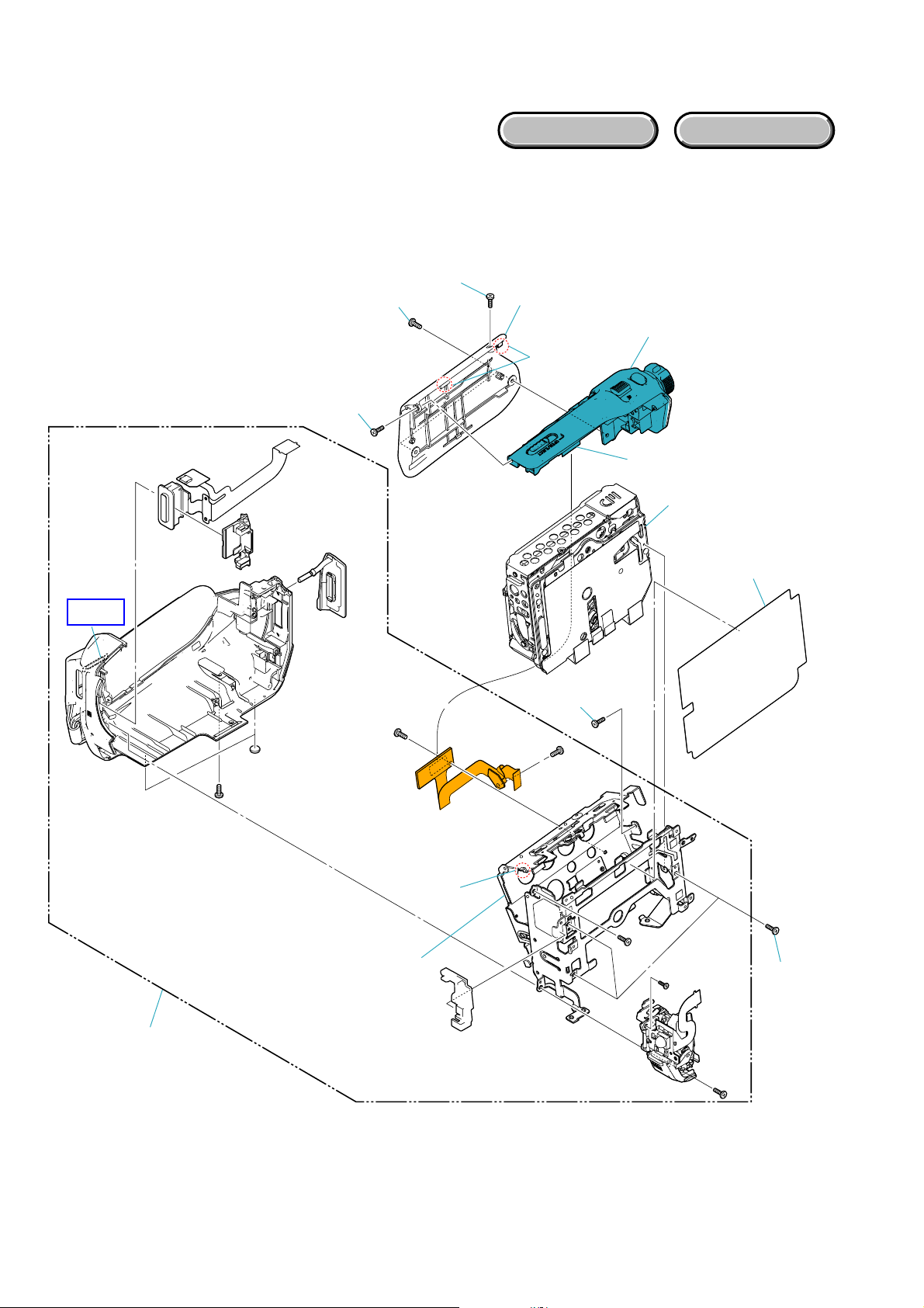
2-1-3. FRONT/BT SECTION
EXPLODED VIEW
Follow the disassembly in the numerical order given.
1 BT Panel Block Assy (1-1 to 1-5)
2 ST-164 Board (2-1 to 2-4)
3 F Panel + Lens Block Assy (3-1 to 3-9)
HARDWARE LIST
3-4
2-4 (#3)
3-1 (#1)
2 ST-164
Board
3 F Panel +
Lens Block Assy
3-9
2-1
2-2
3-6
(#2)
HELP
2-3
3-2
3-3
3-7 (#3)
3-5
Refer to page 2-1 “Note
for disconnecting the
harness (HN-045/HN-046)”.
1-4 (#23)
1-3
HDR-HC5/HC5E/HC7/HC7E_L2
3-8
1-1 (#2)
1 BT Panel Block Assy
2-4
1-5
1-2 (#23)
Page 28
2-1-4. MAIN BOARD SECTION
EXPLODED VIEW
Follow the disassembly in the numerical order given.
1 VC-500 Board (1-1 to 1-14)
HARDWARE LIST
1-14
1-6
1-12
1-8
1-7
1-13
1-5
(HC7/HC7E)
1-9
1-1 (Open)
1-2
(#2)
1-10
(#3)
1-11
(#3)
1-4
1-3
(#9)
HDR-HC5/HC5E/HC7/HC7E_L2
1 VC-500 Board
2-5
Page 29
EXPLODED VIEW
2-1-5. CABINET (L) BLOCK
Follow the disassembly in the numerical order given.
1 Mechanism Deck (1-1 to 1-3)
2 Control Switch Block (2-1 to 2-9)
2-1 (#2)
2-2 (#2)
HARDWARE LIST
2-3 (#2)
2-5
2 Control Switch Block
2-4 (Claw)
2-8
1 Mechanism
Deck
HELP
1-1
2-6 (#23)
2-7 (Claw)
1-3
(Open)
1-2
(#15)
2-9
HDR-HC5/HC5E/HC7/HC7E_L2
2-6
Page 30
2-1-6. FRONT PANEL/LENS SECTION (HC5/HC5E)
EXPLODED VIEW
Follow the disassembly in the numerical order given.
1 Front Panel Block (1-1 to 1-10)
1-10
HARDWARE LIST
1-7 (#3)
1-6
(#3)
1-1
1-8 (Boss)
1-4
1-3
1 Front Panel Block
CM076
1-9
(Boss)
1-2
1-5
(#3)
HDR-HC5/HC5E/HC7/HC7E_L2
2-7
Page 31

EXPLODED VIEW
2-1-7. FRONT PANEL/LENS SECTION (HC7/HC7E)
Follow the disassembly in the numerical order given.
1 Front Panel Block (1-1 to 1-11)
1-11
1-7
(#3)
1-8
(#3)
1-10
(Boss)
HARDWARE LIST
CM-077
1-9
(Boss)
1-4
1-3
1-1
1-2
1 Front Panel Block
1-6(#3)
1-5
HDR-HC5/HC5E/HC7/HC7E_L2
2-8
Page 32

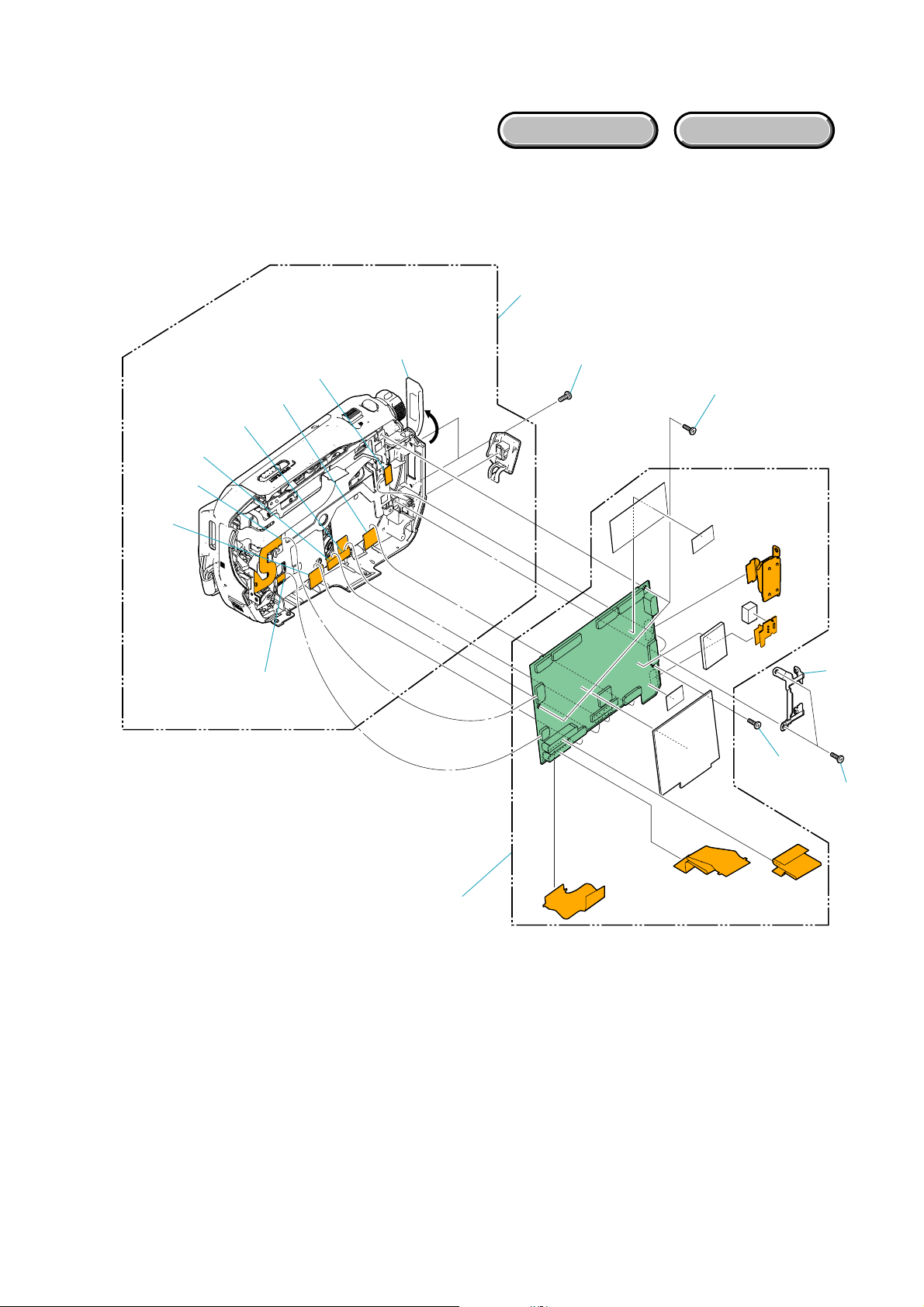
2-1-8. CABINET (R) BLOCK
EXPLODED VIEW
Follow the disassembly in the numerical order given.
1 LCD Block (1-1 to 1-6)
2 Hinge Assy (2-1 to 2-17)
2-4
(#10)
2-5
HARDWARE LIST
2-3
(#10)
2-1 (#23)
2-16 (#10)
2-2
2-6
2-9 (#23)
2-11 (#1)
2-13 (#1)
2-8
HELP
2-7
2-15
2-17
2-14
(Claw)
2-10
2-12
1-1
(#23)
1-6
HDR-HC5/HC5E/HC7/HC7E_L2
2 Hinge Assy
1-2
(#10)
2-9E
1-3
(#10)
1-4
(Claw)
1 LCD Block
1-5
Page 33

HELP
Sheet attachment positions and procedures of processing the flexible boards/harnesses are shown.
THE METHOD OF ATTACHMENT OF FP-659 FLEXIBLE BOARD
1 Fold dotted line parts of the FP-659 flexible board as shown in figure.
Valley fold
Valley
fold
Mountain fold
2 Pass FP-659 flexible board through the flexible clamp
as shown in figure.
Stopper of FP-659 flexible board
Mountain fold
Valley
fold
Stick it together in the adhesive tape
while bending the FP-659 flexible board.
Adhesive tape
Adhesive
tape
3 Install the flexible clamp in the hinge assy
as shown in figure.
Unite
corners.
Flexible clamp
HDR-HC5/HC5E/HC7/HC7E_L2
Concave side
of hinge
Flexible clamp
HELP
Page 34

4 Roll the FP-659 flexible board 2.5 times in the hinge assy and put it on the hinge assy
with the adhesive tape as shown in figure.
Boss
Adhesive Tape
2.5 times
5 Fold dotted line parts of the FP-372 flexible board as shown in figure.
Valley fold
FP-372 flexible board
Switch
6 Install the FP-372 flexible board in the hinge cover (rear) as shown in figure.
FP-372 flexible board
Hinge cover (rear)
Switch
7 Install the hinge cover (rear) in the hinge assy as shown in figure.
Hinge cover (rear)
HDR-HC5/HC5E/HC7/HC7E_L2
Switch
FP-659 flexible board
Plate of hinge
HELP
Page 35

MS-361
board
Loud speaker
Harness arrangement
Harness arrangement
Hook
Cover (CMOS)
assy
Sheet (harness) guard
BT panel block
Front panel block
Lens barrier
flexible board
Tape
Flash unit
Spring
HookHook
HDR-HC5/HC5E/HC7/HC7E_L2
HELP
Page 36

HOW TO REMOVE THE LENS BARRIER ASSY
• NS knob is adjusted to the turning OFF side
• After the hand is affixed under the lens barrier assy,
and the lens barrier assy is pushed on in parallel,
it removes in the direction of the arrow A as shown in figure.
Lens barrier assy
.
NS knob
A
HOW TO INSTALL THE LENS BARRIER ASSY
• NS knob is adjusted to the turning OFF side
• The lens barrier assy is put in the diagonal to avoid
the ground plate andthe NS knob, and the boss is matched.
NS knob
Boss
.
Ground
plate
Boss
Lens barrier assy
HDR-HC5/HC5E/HC7/HC7E_L2
HELP
Page 37

Link
Link
3. BLOCK DIAGRAMS
OVERALL BLOCK DIAGRAM (1/8)
OVERALL BLOCK DIAGRAM (2/8)
OVERALL BLOCK DIAGRAM (3/8)
OVERALL BLOCK DIAGRAM (4/8)
OVERALL BLOCK DIAGRAM (5/8)
OVERALL BLOCK DIAGRAM (6/8)
OVERALL BLOCK DIAGRAM (7/8)
OVERALL BLOCK DIAGRAM (8/8)
POWER BLOCK DIAGRAM (1/5)
POWER BLOCK DIAGRAM (2/5)
POWER BLOCK DIAGRAM (3/5)
POWER BLOCK DIAGRAM (4/5)
POWER BLOCK DIAGRAM (5/5)
HDR-HC5/HC5E/HC7/HC7E_L2
Page 38

3. BLOCK DIAGRAMS
3-1. OVERALL BLOCK DIAGRAM (1/8) ( ) : Number in parenthesis ( ) indicates the division number of schematic diagram where the component is located.
HC5/HC5E HC7/HC7E
LENS BLOCK
IRIS
(SHUTTER)
SE8201
YAW SENSOR
SE8202
PITCH SENSOR
LD-221 BOARD (1/3)
IRIS
METER
ND FILTER
METER
FOCUS
MOTOR
FOCUS MR
SENSOR
ZOOM
MOTOR
ZOOM MR
SENSOR
NF MOTOR
LENS TEMP
SENSOR
LENS BARRIER
LENS COVER
MOTOR
LENS COVER
SENSOR
05
I_DRIVE±
M
I_BIAS±
H
I_HALL±
ND_DRIVE±
M
ND_BIAS±
H
ND_HALL±
M
M
M
FOCUS ±
F_MR_A,
F_MR_B
ZOOM_A,
ZOOM_B,
Z00M_XA,
ZOOM_XB
Z_MR_A,
Z_MR_B
NF_DRIVE± NF_EN, NF_SW
TEMP_OUT
UNIT
MM
OPEN
CN5302
7, 12, 43, 514, 811, 912, 10
IC5401
7, 1
NOISE FILTER
29, 2824 - 2730 - 33 21, 1918, 16
23
CN5305
1 - 4
8
(1/3)
IC5402 IC5403
7, 1
NOISE FILTER
(1/3)
SHUTTER_A, SHUTTER_B,
SHUTTER_XA, SHUTTER_XB
LENS_COVER_OPEN LENS_COVER_OPEN
2
2
IC6901
4M CMOS
IMAGER
10
IC8201
PITCH/YAW
SENSOR
6
AMP
IC5404
(1/3)
IRIS
DRIVE,
HALL
AMP
ND
FILTER
DRIVE,
A11, A9C10, B11E12, E10
HALL
AMP
F3
FOCUS
MOTOR
DRIVE
B1, C4
ZOOM
F1, K6L6, L7 H1, J1C6, A5C5, B6K2, L2
MOTOR
DRIVE
NF MOTOR
DRIVE
IC5801
LENS COVER
MOTOR
DRIVER
F2, F3, E6, D6
(3/3)
7, 8, 42, 419, 10, 40, 39 11, 12, 38, 37
23
16, 17
27
19, 18, 15
16
20
17
C9
A4
A10
D10
K12
L12
K11, J11, H12
J12
H11
K9, L9, M9, J9
L8, M8
B6, C6, C5
CN6801
27 - 3023 - 26 19 - 22
17
5, 4
11
AHS_SO, AHS_SCK, XCS_AHS
1 - 3
8
7
9
FP-648 FLEXIBLE BOARD (1/4)
CN5303
(1/3)
42
25
CAM_SI, CAM_SO, XCAM_SCK
33, 30, 32
14
12
16, 1726 - 28 24, 31, 29
18
23
DRVOUT1, DCOUT1,
DRVOUT4, DCOUT4
DRVOUT3, DCOUT3,
DRVOUT6, DCOUT6
DRVOUT2, DCOUT2,
DRVOUT5, DCOUT5
CHCK2_4M
TGHD, TGVD
XSYS_RST
YAW_AD
PITCH_AD
VST_C_RESET
PNDCK
CAM_VD
XCS_IC_5404
XRST_IC_5404
EN1, DIRA1, DIRB1
LENS_TEMP_AD
EN0, DIRA0, DIRB0
1
2
5
6
OVERALL (2/8)
(PAGE 3-2)
OVERALL (2/8)
(PAGE 3-2)
OVERALL (2/8)
(PAGE 3-2)
OVERALL (2/8)
(PAGE 3-2)
LENS BLOCK
(SHUTTER)
ND FILTER
METER
FOCUS
MOTOR
ZOOM
MOTOR
ACTIVE LENS
ACTUATOR
PITCH
MOTOR
YAW
MOTOR
IRIS
IRIS
METER
M
H
M
H
M
FOCUS MR
SENSOR
M
ZOOM MR
SENSOR
NF MOTOR
M
LENS TEMP
SENSOR
THERMISTOR
M
H
M
H
I_DRIVE±
I_BIAS±
I_HALL±
ND_DRIVE±
ND_BIAS±
ND_HALL±
FOCUS ±
F_MR_A,
F_MR_B
ZOOM_A,
ZOOM_B,
Z00M_XA,
ZOOM_XB
Z_MR_A,
Z_MR_B
NF_DRIVE± NF_EN, NF_SW
TEMP_OUT
THERM
PITCH±
PITCH_IN±
PITCH_OUT±
YAW±
YAW_IN±
YAW_OUT±
CM-076 BOARD
CM-077 BOARD
YAW SENSOR
PITCH SENSOR
LD-221 BOARD (1/3)
CN5301
7, 12, 43, 514, 811, 912, 10
24, 2548 - 5126 - 29 16, 1820, 2132, 3833, 39
IC5402 IC5403
7, 1
NOISE FILTER
(1/3)
23
31
PITCH±
40 - 43
PITCH_HALLBIAS±
PITCH_HALL±
44 - 47
36, 3734, 35
YAW±
YAW_HALLBIAS±
YAW_HALL±
SE7201
SE7202
2
IC6701
6.1M CMOS
IMAGER
10
IC7201
PITCH/YAW
SENSOR
6
AMP
IC5404
(1/3)
IRIS
DRIVE,
HALL
AMP
ND
FILTER
DRIVE,
A11, A9C10, B11E12, E10
HALL
AMP
FOCUS
F3, E3
MOTOR
DRIVE
B1, C4
ZOOM
MOTOR
F1, K6
DRIVE
NF MOTOR
DRIVE
L6, L7 H1, J1C6, A5C5, B6K2, L2
IC5703
OPTICAL
J3, J2 B1, D1H2, J4
IMAGE
STABILIZATION
DRIVER
(2/3)
B10, D10
G6, J8
J9, J7
46, 45, 27, 2844, 43, 29, 3042, 41, 31, 32
40, 39, 33, 34
2
4, 5
10
6 - 8
16
20
17
C9
A4
A10
D10
K12
L12
CAM_SI, CAM_SO, CAM_SCK
K11, J11, H12
J12
H11
K9, L9, M9, J9
L8, M8
C9
A5
B4, A4, B5
A6
A7
A3
D5
G5
J5
CN6601
37 - 4029 - 3222 - 25
18 - 21
16
5, 4
11
AHS_SO, AHS_SCK, XCS_AHS
1 - 3
8
7
9
FP-648 FLEXIBLE BOARD (1/4)
CN5303
(1/3)
22
19
42
25
CAM_SI, CAM_SO, XCAM_SCK
33, 30, 32
14
12
16, 1726 - 28 24, 31, 29
18
15
CAM_SI, CAM_SO, CAM_SCK
11
13
35
8
9
10
DRVOUT4, DCOUT4,
DRVOUT8, DCOUT8
DRVOUT3, DCOUT3,
DRVOUT7, DCOUT7
DRVOUT2, DCOUT2,
DRVOUT6, DCOUT6
DRVOUT1, DCOUT1,
DRVOUT5, DCOUT5
CHCK3_6M
TGHD, TGVD
XSYS_RST
YAW_AD
PITCH_AD
VST_C_RESET
IR_NOISE
ND_NOISE
PNDCK
CAM_VD
XCS_IC_5404
XRST_IC_5404
EN1, DIRA1, DIRB1
LENS_TEMP_AD
THERM
XRST_IC_5703_CPU
XDS_RESETXHIDS_RST
DSCK_IC_5703
VST_C_RESET
PITCH_AD
YAW_AD
3
4
7
8
9
OVERALL (2/8)
(PAGE 3-2)
OVERALL (2/8)
(PAGE 3-2)
OVERALL (2/8)
(PAGE 3-2)
OVERALL (2/8)
(PAGE 3-2)
OVERALL (2/8)
(PAGE 3-2)
A : VIDEO SIGNAL
HDR-HC5/HC5E/HC7/HC7E_L2
LENS BARRIER
LENS COVER
MOTOR
LENS COVER
OPEN
SENSOR
UNIT
CN5305
SHUTTER_A, SHUTTER_B,
MM
SHUTTER_XA, SHUTTER_XB
1 - 4
LENS_COVER_OPEN LENS_COVER_OPEN
8
IC5801
LENS COVER
MOTOR
DRIVER
F2, F3, E6, D6
(3/3)
B6, C6, C5
EN0, DIRA0, DIRB0
OVERALL (2/8)
10
(PAGE 3-2)
23
3-1
Page 39

3-2. OVERALL BLOCK DIAGRAM (2/8)
HC5/HC5E
OVERALL (1/8)
(PAGE 3-1)
1
HC7/HC7E
OVERALL (1/8)
(PAGE 3-1)
3
A : VIDEO SIGNAL
HC5/HC5E
OVERALL (1/8)
(PAGE 3-1)
2
HC7/HC7E
OVERALL (1/8)
(PAGE 3-1)
4
FP-648 FLEXIBLE BOARD (2/4)
HC7/HC7E
OVERALL (1/8)
(PAGE 3-1)
7
HC5/HC5E
OVERALL (1/8)
(PAGE 3-1)
5
HC7/HC7E
OVERALL (1/8)
(PAGE 3-1)
8
DRVOUT1, DCOUT1, DRVOUT4, DCOUT4
DRVOUT3, DCOUT3, DRVOUT6, DCOUT6
DRVOUT2, DCOUT2, DRVOUT5, DCOUT5
CHCK2_4M
DRVOUT4, DCOUT4, DRVOUT8, DCOUT8
DRVOUT3, DCOUT3, DRVOUT7, DCOUT7
DRVOUT2, DCOUT2, DRVOUT6, DCOUT6
DRVOUT1, DCOUT1, DRVOUT5, DCOUT5
CHCK3_6M
TGHD, TGVD
XSYS_RST
AHS_SO, AHS_SCK, XCS_AHS
YAW_AD
PITCH_AD
VST_C_RESET
IR_NOISE
ND_NOISE
PNDCK
CAM_VD
XCS_IC_5404
XRST_IC_5404
EN1, DIRA1, DIRB1
CN1201
12 - 936,37
14
19 - 16
23 - 20
25
30
40 - 38 4 - 18 - 5
33
34
32
CN1010
(1/3)
30
33
10
27
19, 22, 20
38
40
VC-500 BOARD (1/7)
CHCK
YAW_AD
PITCH_AD
VST_C_RESET
EN1, DIRA1, DIRB1
( ) : Number in parenthesis ( ) indicates the division number of schematic diagram where the component is located.
K10, K9
J10, J9,
B10, B9
A10, A9,
F10, F9
E10, E9,
IC1201
CDS,
A/D
CONVERTER
(1/20)
K10, K9
J10, J9,
B10, B9
A10, A9,
IC1301
CDS,
A/D
CONVERTER
(2/20)
X1701
80.9191 MHz : HC5
62.3700 MHz : HC5E
89.010989 MHz : HC7
74.25000 MHz : HC7E
CAM_SI, CAM_SO, XCAM_SCKCAM_SI, CAM_SO, XCAM_SCK
K2 - K4
J2 - J4,
F3 - F5,
A3 - D3,
K2 - K4
J2 - J4,
F3 - F5,
A3 - D3,
A_2.8V
TG_FLD
CAM_VD_HS
CAM_VD
H3, H4
G3 - G5
A5 - E5
A4 - E4,
B2 - H2
B1 - H1,
ADC_SO, ADC_SCK, XCS_ADC0
F7, E6, E7
H5
ADC_TGHD, ADC_TGVD
G6, F6
D6
D7
K5
H3, H4
G3 - G5
A5 - E5
A4 - E4,
ADC_SO, ADC_SCK, XCS_ADC0
F7, E6, E7
H5
ADC_TGHD, ADC_TGVD
G6, F6
D6
D7
K5
1 5
D13
D7
A7
P20
AB10
AB11, Y11,
C22
B14
CLPOB
XSYS_RST
CAM_VD_HS
CHCK
AD1_0 - AD1_13
AD3_0 - AD3_13
CLPOB
XSYS_RST
CAM_VD_HS
CHCK
IC1701
CLOCK
GENERATOR
(3/20)
AA2, Y2,
IC1801
CAMERA
CONTROL
(16/20)
AD0_0 - AD0_13
AD2_0 - AD2_13
AD1_0 - AD1_13
XSYS_RST
AHS_TGHD, AHS_TGVD
AHS_SO, AHS_SCK, AHS_XCS0
CHCK
PNDCK
EN1, DIRA1, DIRB1
CAM_VD
CAM_VD_HS
TG_FLD
J1
K1
P2, P1, N4,
N2, N1, M4
V4, V2, W1,
W4, W2, Y1,
F2
F4
ZOOM_SW_AD ZOOM_SW_AD
M22
SIRCS_SIG SIRCS_SIG
A10
NTSC/XPAL_DET NTSC/XPAL_DET
A17
SYS_V SYS_V
B8
XCS_IC_1702_BUS
IC_1702_BUS_CLK
D24A00_CAM - D31A07_CAM,
DXXA08_CAM - DXXA13_CAM
AA13 - AA16,
AB12 - AB16,
AC14 - AC17,
U22, U23,
V21 - V23,
AA21 - AA23,
AA17 - AA20,
AB17 - AB21,
AC18 - AC21,
P21 - P23,
N21 - N23,
R21 - R23,
G23, J22, H21
K21
K23, M22J23, L22
AB4
T4
H23, K22, J21G22, E23, F21
U1
AC11
AC7
AA6
L21
AA3
AC5
AA7 - AA9,
AB8 - AB10,
AA11, AA12,
Y13
Y21 - Y23
W21 - W23,
Y17
IC1702
CAMERA
SIGNAL
PROCESSOR
(3/20)
U20, U21
T21 - T23,
A16 - A21,
A5, A6, A8,
Y10, Y12
AC13, Y8,
AC8, AC9,
E2, E1,
D3 - D1,
H1,
G4 - G1,
A3
A10
D9
C4 - C9,
B17 - B22,
B4, B6 - B9,
C17, C18, C20,
A11 - A15,
B12, B13, B15,
C12, C13, C15,
F23
H22
C3 - C1
F3 - F1
H4 - H2
HDI_Y0 - HDI_Y7
HDI_C0 - HDI_C7
HDI_HD, HDI_VD, HDI_OE
VCK
HC5/HC5E
IC1902
128M SDRAM
(3/20)
A8, B9, B8, C9,
H7, H8, J8, J7,
C8, D9, D8, E9,
J3, J2, H3 - H1,
E1, D2, D1, C2,
G9
F2
F2
SD_CK
SD_XCS
SD_CKE
SD_DQ0 - SD_DQ31 SD_DQ0 - SD_DQ15
D6, D7, D17
D12, D13, D15
SD_A0 - AD_A11, SD_BA0, SD_BA1
J8J1J2
G3, H9, G2, G7,
C1, B2, B1, A2
SD_DQ00 - SD_DQ31 SD_DQ0 - SD_DQ15
G8, G9, F7, F3, G1,
R8, N7, R9, N8, P9, M8,
G2, G3, H1, H2, J3,
M7, L8, L2, M3, M2, P1,
N2, R1, N3, R2, E8, D7,
D8, B9, C8, A9, C7, A8,
256M SDRAM
A2, C3, A1, C2,
B1, D2, D3, E2
IC1901
(3/20)
G7, H9, J7, H8
G8
HC7/HC7E
U1R1
AE23
V22
STROBE_ON
EXT_STROBE_ON
XSYS_RSTXSYS_RST
Y19, AD22,
AE20, W19,
AA22, AD23
AC19, AE21,
Y17, AC17,
Y18, AD20,
AB18, AC18
AD19, W18,
AC22
AE22, AC20,
IC2101
(1/5)
BASE BAND
SIGNAL
PROCESSOR
(4/20)
R19, T22, T24, T25,
R22, R23, P24, N19
T20, V25, U25, U23,
T23, P19, R20, N24,
Y25, U20
Y24, W22, U19,
AC25, V19, V20,
W20, AB25, Y23,
AB23, AD24, AB24,
11
OVERALL (8/8)
(PAGE 3-8)
HDR-HC5/HC5E/HC7/HC7E_L2
HC5/HC5E
OVERALL (1/8)
HC7/HC7E
OVERALL (1/8)
HC7/HC7E
OVERALL (1/8)
05
(PAGE 3-1)
(PAGE 3-1)
(PAGE 3-1)
10
NF_EN, NF_SW
LENS_TEMP_AD
6
9
EN0, DIRA0, DIRB0
LENS_COVER_OPEN
THERM
XRST_IC_5703_CPU
XDS_RESET
DSCK_IC_5703
VST_C_RESET
PITCH_AD
YAW_AD
36, 3525, 24, 26 28, 21, 23
34
CAM_EN0,
CAM_DIRA0, CAM_DIRB0
29
37
41
39
17
VST_C_RESET
44
PITCH_AD
43
YAW_AD
42
PITCH_AD
YAW_AD
VST_C_RESET
HC5/HC5E
N22, N20
R22
A14, A13,
B5
F23
P22
P23
T2
D12
XSLOWSHUT_NR
B13
HI_SI, HI_SO, XHI_SCK
Y7, AB7, AB6
XCS_CAMERA
AC6
C1
X1801
20MHz
D1
XCS_EEP_C
F1
AB13,
EEP_SI_C,
AB14, AC14,
EEP_SO_C,
EEP_SCK_C
IC1802
1
128k EEPROM
(16/20)
2, 5, 6
HI_SI, HI_SO, XHI_SCK
SYS_V
XSLOWSHUT_NR
XCS_CAMERA
XDS_RESET
DSCK_IC_5703
12
13
14
15
OVERALL (5/8)
(PAGE 3-5)
OVERALL (6/8)
(PAGE 3-6)
HC7/HC7E
OVERALL (8/8)
(PAGE 3-8)
OVERALL (4/8)
(PAGE 3-4)
3-2
Page 40

3-3. OVERALL BLOCK DIAGRAM (3/8)
VC-500 BOARD (2/7)
RYI0 - RYI3
L2, M7
IC2101
(2/5)
BASE BAND
SIGNAL
PROCESSOR
(4/20)
L4, K7,
M2, M3,
P2, N1,
P1, P4,
L24
N22
F10
C10
A3
B17, F17,
C18, F18,
A19, G17,
C21, C20,
B19, D19,
B20, D20,
B24
D23
B21
L1
K1
P25
M25
Y16
F8
D9
G9
N2, M1
K2, L3
M20, L20
P6, R2
T2, R4
N3, P3
A20, C19
C22, G20
A22, D21, B22
L19, K24
P23, M24
DV PB
RCI0 - RCI3
HYI, HCI
ADATAOUT0, ADATAOUT1
RYO0 - RYO3
DV REC
RCO0 - RCO3
HYO, HCO
FS_EDGE_REF
FRAT_REFO
THYRQ_FVDI
THCRQ_FHDI
TFS_FCO
MFLG_QRST
FLAT_SYNC_FYO0
VLAT_SYNC_FCI
VLAT_IN_FYO1
IC_2201_YO0 - IC_2201_YO7
HDV REC/PB, HDV-i.LINK
IC_2201_CO0 - IC_2201_CO7
TRN_HD, TRN_VD, TRN_FLD
TRN_VF_SYNC
CKTRNO
CKTRNI
ADATAIN0, ADATAIN1
AUIN21, AUIN22
CK27MFO1
CKFSO
CK64FSO
MCLK
IC_2101_PCRERR
IC_2101_SRCH
IC_2101_FLD27MF
( ) : Number in parenthesis ( ) indicates the division number of schematic diagram where the component is located.
C23, D21
E24, E21,
D23, E23,
D20, D24,
A21, B18
B21, B20,
D18, C24,
B23, D17,
E14 - E16
E18
F24
HDV-MPEG VIDEO
A22
ENCODER/DECODER,
MPEG AUDIO
SIGNAL PROCESSOR
M23, M21N23, N211
A20
P21
M24
P24
Y13, AC13,
AA14, AC14,
IC2201
(5/20)
AD6, AC4, AD5, AC5, AD4,
AA5, AD3, AB2, Y8, W2, Y9,
U2, AA2, W1, V2, V1, G1, H1,
T1, U1, T2, R4, R2,
AD15, AC16
AA15, AC15,
AD12
AD16
AD17
AA16, Y17AC17, AC18
AD18
BMDT16 - BMDT47
F1, H2, E2, D2, F2, G2, D7,
A4, B5, A5, B7, B6, D8, A6,
OMAD00 – OMAD12,
OMADB0, OMADB1
P2, P1, N1, L5, M4
R1, P5, N5, N2, M2,
OMCEX
J1
OMCKE
L2 G1
OMCLK
L1
OMCLKX
K1 G3
RYI0 - RYI3
DV PB
RCI0 - RCI3
HYI, HCI
ADATAOUT0, ADATAOUT1
RYO0 - RYO3
DV REC
RCO0 - RCO3
HYO, HCO
ADATAIN0, ADATAIN1
FS_EDGE_REF
FRAT_REFO
THYRQ_FVDI
THCRQ_FHDI
TFS_FCO
MFLG_QRST
FLAT_SYNC_FYO0
VLAT_SYNC_FCI
VLAT_IN_FYO1
CK64FSO
CKFSO
CK27MFO1
HDV REC/PB, HDV-i.LINK
EBS[0] - EBS[7]
KCLK
ERDY
ERE
AUDAI, AUENI
AUDAO, AUENO
C3, B2, B3, A2
P3, R2, A8, B7, B8, C7, C8,
D7, D8, E7, E3, D2, D3, C2,
L7, L3, M2, M3, N2, N3, P2,
R8, P7, P8, N7, N8, M7, M8,
K3, J1, J2, J3, H1,
J8, J9, K7, K9, K1,
J7, H2, H3, H8, H9
H7
IC2401
256M
G2
DDR-SDRAM
(5/20)
IC_2101_PCRERR
IC_2101_SRCH
IC_2101_FLD27MF
A5, B5,
A7, C7,
F7, C8
C4, D3
E9, B9,
B11, C11,
A9, B10
E1, E3
C1
D2
A8
F9
C10
A3N7
F6B9
F3A9
F2F9
M3
L1
F1
M1
C18, F18,
A20
F16
F19
B16, C16B19, C19
C5
B3
G3
A4, B4
C6, B6
F8, C9
A10, E10
HDV STREAM
MUX/DEMUX,
F17, B17
B18, E19,
A18, C17,
IC2701
PROCESSOR,
DV SIGNAL
PROCESSOR
(6/20)
R1
W6
W1
U3, V3
U20, U24
V23, V20,
V25, U23,
V24, W21,
T25
T23
R20
P20
U21
R25
C25
D23
D25
F23
F24
G23
J3
H24
A23
H23
FRRV, TRRT, TRRV, DRP
C24, E25
E24, D24,
DXXA00_SIM - DXXA10_SIM
M23, M24
R21, N20, P21,
N25, L20, M25,
N21, M20, N23,
D24A00_SIM - D31A07_SIM
J20, K23
K20, L24,
L23, K25,
K21, K24,
HDV-i.LINK,
DV-i.LINK
PD00 - PD07
PCLK0
IDIR0
XPEN0
XIACC0
FCLR0
FR1
X3401
24.576 MHz
L11, K11,
L8
E12
M8
L9
M9
J8
J9
C1
C2
H11, G9
H9, H12,
K12, J11,
HDV/DV
INTERFACE
IC3401
i.LINK
(7/20)
HDV PB, DV PB
HDV REC, DV REC
A4 - A7
B8
E2
J6
D7
E7, E6,
D8, E11
J2, K2
F1, F2,
H2, J1,
G2, H1,
L6, L7
L2, L3,
M3, L4,
M4, M6,
D12
TRRT
HDV-i.LINK, DV-i.LINK
TPA+, TPA-, TPB+, TPB-
D24A00_SIM - D31A07_SIM
DXXA00_SIM - DXXA07_SIM
FRRV, TRRT, TRRV, DRP
DXXA00_SIM - DXXA10_SIM
D24A00_SIM - D31A07_SIM
A : VIDEO SIGNAL
A : AUDIO SIGNAL
A : VIDEO/AUDIO SIGNAL
A : VIDEO/AUDIO/SERVO SIGNAL
RFIN
RECDT
RECCK
RECA1, RECA2
16
17
IC_3401_PLL_ON
XCS_IC_3401
XRST_LINK
XRST_PHY
PWD, CNA, LPS, OFR2
SWP
ATF_LATCH
SCWIN
XCS_IC_2701_HD
XCS_IC_2701_DV
XRST_IC_2701_DV
XRST_IC_2701_1
XRST_IC_2701_2
18
OVERALL (5/8)
(PAGE 3-5)
OVERALL (7/8)
(PAGE 3-7)
OVERALL (5/8)
(PAGE 3-5)
05
HDR-HC5/HC5E/HC7/HC7E_L2
D24A00_SIM - D31A07_SIM
R23, R24
T20, T21,
T23, T24,
R20, R21,
ALE_SIM
N24
XCS_IC_2201
M20
XRST_IC_2201
D16
INT_IC_2201
P20
FRRV, TRRV, DRP
W17, W16, N20
DXXA08_SIM, DXXA09_SIM
W13, AD13
D24A00_SIM - D31A07_SIM
Y14, AD15,
W14, AB13,
AE13, AD14
AD16, AB14,
ALE_SIM
Y15
SD_OSD_VD
AC14
VREF
AE15
IC_2101_OEREF
AB16
XCS_IC_2101_SIM
AC15
XRST_VTR XRST_VTR
D17
3-3
ALE_SIM
XCS_IC_2201
XRST_IC_2201
INT_IC_2201
MCLK
SD_OSD_VD
VREF
IC_2101_OEREF
XCS_IC_2101_SIM
CKFSO
CK64FSO
19
OVERALL (4/8)
(PAGE 3-4)
Page 41

3-4. OVERALL BLOCK DIAGRAM (4/8)
( ) : Number in parenthesis ( ) indicates the division number of schematic diagram where the component is located.
VC-500 BOARD (3/7)
IC2101
(3/5)
BASE BAND
SIGNAL
PROCESSOR
(4/20)
J1, K6,
H1, J7,
D3, F3,
G6, C3,
G4, F2,
H7, G2,
HM_Y0 - HM_Y7
G1, J6
H4, H2,
HM_R0 - HM_R7
C1, E3
E4, D2,
HM_B0 - HM_B7
E2, F4
H6, E1,
HM_HD, HM_VD
C2, D5
IC_2101_ADAO2
N25
IC_2101_ADAO1
M19
CK_HM
J3
CK74MFO
J2
CK256FSO
C24
HM_Y0 - HM_Y7
HM_R0 - HM_R7
HM_B0 - HM_B7
HM_HD, HM_VD
IC_2101_ADAO2
IC_2101_ADAO1
CK_HM
CK74MFO
CK256FSO
CK64FSO
CKFSO
D12, C12,
D1, C1,
B8 - B5,
C7, C6
E9
C11
E1
G1
D10
E10
E11
A10, A9
B12 - B9,
A4 - A2
B4 - B2,
A8 - A5
IC3101
HDMI
SIGNAL
PROCESSOR
(8/20)
K2, K12,
L1 - L11,
M3 - M11
J12, J1, K1,
J9, K10G9, G10
F12
H12
G11
F10
J10
F4
C2
D3, D2, F2
DE_HDMI, D0_HDMI - D23_HDMI
HSYNC_HDMI, VSYNC_HDMI
ADAO1_HDMI, ADAO2_HDMI
IDCK
256FS_HDMI
64FS_HDMI
FS_HDMI
HDMI_SDA, HDMI_SCL
HDMI_SDA, HDMI_SCL
XRST_HDMI
XCS_IC_3101
VSP_SI, VSP_SO, XVSP_SCK
C2, A1 - A10,
B1 - B10, C9,
C10, D9, D10
C1, D2
TRANSMITTER
F2, F1
D1
E1
H2
H1
F9, F10
IC3201
HDMI
(8/20)
21
K5, K4, K8,
K7, J10, K10
K2, K1
K3
G9, G10
OVERALL (5/8)
(PAGE 3-5)
CN3202
FP-645 FLEXIBLE
BOARD
TMDS DATA0± - TMDS DATA2±
12, 11, 15, 14, 18, 17
TMDS CLOCK±
9, 85, 6
2
HPD
SDA, SCL
CN001
19
7, 9, 4, 6, 1, 310, 1216, 15
A : VIDEO SIGNAL
A : AUDIO SIGNAL
A : VIDEO/AUDIO SIGNAL
HDMI
OUT
IC_2101_ADAO1
CK256FSO
CK13MFO1
F21, J21,
K20, F19,
F20, G20,
J20, G19,
K18, H18,
L20, V20, V21,
T19, M18, R19
U20, P19, N18,
P18, W21, U19,
W20, N19, R18,
IC5101
(1/3)
DS CONTROL
(14/20)
CK64FSO
CKFSO
OVERALL (5/8)
(PAGE 3-5)
J19, J18
M2
L1
A15
Y18
P1, N1
USB_DET
A14, C15, D14
OVERALL (3/8)
(PAGE 3-3)
W4, AA2,
AE2, AC1,
AA4, AC3,
AB3, AC2,
AD3, AD2,
W8, AD6, Y7,
AE8, Y10, Y9,
AB8, W9, AE6,
AD7, AB6, AE5,
AD8, AC8, AC7,
R1
U2
C4
AE3
DSCK_VM
AD10
U6, T4, T6
Y3, Y1, T7,
AD4
AE4, AC6, AC5,
HC7/HC7E
OVERALL (2/8)
(PAGE 3-2)
OVERALL (8/8)
(PAGE 3-8)
05
15
20
DSCK_IC_5703
XSYS_RST
13
19
A1_VM - A21_VM
2 - 11,
20 - 27,
30, 31, 55
IC5202
32M FLASH
(15/20)
CK64FSO
CKFSO
D0_VM - D15_VM
33 - 36,
39 - 46,
49 - 52
DACK1_IC_2101DACK1_IC_2101
XCS_IC_2101_VMXCS_IC_2101_VM
DSCK_VM
D0_VM - D15_VMD0_VM - D15_VM
A1_VM - A21_VMA1_VM - A19_VM
A13_VM
A1_VM - A11_VM,
19 - 24,
27 - 32
15
19
D0_VM - D15_VM
2, 3, 5, 6, 8, 9, 11,
12, 39, 40, 42, 43,
45, 46, 48, 49
IC5201
16M SDRAM
(15/20)
35
34
18
CKE_VM
XCS_SDRAM
XCS_FLASH_UTA
D12
B16
A10
H19, K21,
K19, H20,
Y19, W18, M19,
W19, AA19, AA18,
C18
C17
A18
OVERALL (7/8)
22
(PAGE 3-7)
OVERALL (5/8)
23
(PAGE 3-5)
RF_MON
SWP
24
USB_D±
X5101
24
IC5103
OSCILLATOR
DRIVE
(14/20)
MS_DIO, MS_BS, MS_SCLK
Q5101
LED
DRIVE
48 MHz
MS_LED_ON
MS-361 BOARD
24
26
21, 22
19
8, 10, 3
6
13
(1/3)
CN8001
(1/3)
(MS ACCESS)
CN8003
CN8004
DIO, BS, SCLK
D8003
FP-649
FLEXIBLE
CN1012
BOARD (1/3)
(1/3)
RF_MON
24
SWP
26
USB_D±
21, 22
USB_DET
19 8
8, 10, 3
MS_INSERTXMS_IN
6
XACCESS_LED
13
INS
1
6
3, 4
4, 2, 8
US-013 BOARD
CN8101
36
18
6, 5
D8101
MEMORY
STICK
DUO
CN8103
RF_MON
SWP
CN8102
D±
VCC
1
2
(FOR CHECK)
3, 2
1
CPC
(USB)
HDR-HC5/HC5E/HC7/HC7E_L2
3-4
Page 42

3-5. OVERALL BLOCK DIAGRAM (5/8)
VC-500 BOARD (4/7)
OVERALL (4/8)
(PAGE 3-4)
OVERALL (4/8)
(PAGE 3-4)
OVERALL (8/8)
(PAGE 3-8)
OVERALL (3/8)
(PAGE 3-3)
OVERALL (4/8)
(PAGE 3-4)
OVERALL (7/8)
(PAGE 3-7)
OVERALL (7/8)
(PAGE 3-7)
OVERALL (7/8)
(PAGE 3-7)
24
23
25
18
21
26
27
28
RF_MON
SWP
F1
XRST_VTR
IC2402
16M FLASH
(17/20)
B4
FLASH_A15 - FLASH_A20
B2, C3, D4
C6, D6, E6,
DXXA00_SIM - DXXA14_SIM
D5, B6, A6
A2, B5, A5, C5,
G6, E1, D1, C1,
A1, B1, D2, C2,
D24A00_SIM - D31A07_SIM
H2 - H5
E2 - E5,
NTSC/XPAL_DET
XSYS_RST
XRST_VTR
IC_3401_PLL_ON
XCS_IC_3401
XRST_LINK
XRST_PHY
PWD, CNA, LPS, OFR2
SWP
ATF_LATCH
SCWIN
XCS_IC_2701_HD
XCS_IC_2701_DV
XRST_IC_2701_DV
XRST_IC_2701_1
XRST_IC_2701_2
FRRV, TRRT, TRRV, DRP
DXXA00_SIM - DXXA10_SIM
D24A00_SIM - D31A07_SIM
ALE_SIM
XCS_IC_2201
XRST_IC_2201
INT_IC_2201
MCLK
SD_OSD_VD
VREF
IC_2101_OEREF
XCS_IC_2101_SIM
HDMI_SDA, HDMI_SCL
XRST_HDMI
XCS_IC_3101
VSP_SI, VSP_SO, XVSP_SCK
VSP_SO, XVSP_SCK
XCS_AUVOL
XLINE_CNT1A, XLINE_CNT1B, XLINE_CNT2,
XLINE_CNT3A, XLINE_CNT3B
XD4CN
XPSV_D4
DEM0, DEM1
XPWAD, XPWDA
XCS_IC_3001
HP_JACK_IN
XRST_VTR
XCS_FLASH
HC7/HC7E
HC7/HC7E
( ) : Number in parenthesis ( ) indicates the division number of schematic diagram where the component is located.
X4401
20MHz
A18, B5, A5
H2
AB5, Y5, AB4,
AB3, AC3, AB2
D1
C1
B4
F2
F4
Y18
F23
J2
E20
D22
A14, D9
Y10, AC9,
B21
B22
D18
H4
G1
G2
D13
B13
A16, A21
B18, D15,
T4, T2, U1,
U4, U2, V1,
R4, R2, P2,
Y1, V4,
W4, W2,
AA2, Y2,
K4
J1
E22
A6
K1
B8
B7
Y8
G4
D10, B10
Y15
AB10
AC7
AC8, AB8,
B19
N20
P20, F20,
P22, P23,
R22
N23
AC10, L23
AB17, Y17
AC17
D23
IC4401
MECHA
CONTROL
(17/20)
P1, N4, N2,
N1, M4, M2
V2, W1
RF_MON
CONT1, SW_PS, ALL_PSCONT1, SW_PS, ALL_PS
HDV PB, DV PB
(1/2)
RFIN
HDV REC, DV REC
RECDT
RECCK
RECA1, RECA2
C15, B15A13, A14
Q4607, Q4609
DRUM
PWM DRIVE
Q4608, Q4610
CAPSTAN
PWM DRIVE
CK13MFO1CK13MFO1
XRST_VTR
VSP_SO, XVSP_SCK
XCS_IC_4801
AB9
DRUM_PWM
Y14
CAP_PWM
AC15
XFFREWUP
AC13
A9
B9
CAP_FWD, CAP_ON
D19, B20
D11
DEW_DET
V23
MODE_SW_A - MODE_SW_C
AB22
-
AB20
LOAD, UNLOAD
D16, A17
LM_LIM_DET LM_LIM_DET
L22
TAPE_END
AB11
TAPE_TOP
Y11
TREEL_FG
B11
SREEL_FG
A11
TAPE_LED_ON
B15
D14
V22
Y12
Y13, AC12,
D6
D8
K22
AC6
AB6
Y7, AB7,
Y22, Y23
35
34
IC4801
38, 36
(3/3)
(13/20)
SERIAL
37
INTERFACE
44
41
Q4801
HOTSHOE_ID1, HOTSHOE_ID2
45
LPF
43
XSLOWSHUT_NR
VD_SI, VD_SO, XVD_SCK
EVF_OUT_EN
XCS_IC_4401
HI_SI, HI_SO, XHI_SCK
REC_PROOF
CHIME_SDA, CHIME_SCK
DRUM_ERROR
CAP_ERROR
DRUM_FG
DRUM_PG
CAP_FG
SYS_V
XCS_EVF
XCS_LCD
XCC_DOWN
OVERALL (3/8)
(PAGE 3-3)
E15
C14
B12
A11
OVERALL (2/8)
12
(PAGE 3-2)
OVERALL (6/8)
29
(PAGE 3-6)
OVERALL (8/8)
30
(PAGE 3-8)
16
IC4601
DRUM/
CAPSTAN
PWM DRIVER
(19/20)
SWP
30
38
39, 37, 45
35
46
44
40, 42
IC4901
REC/PB AMP
(12/20)
Q4803
DRIVE
CAP_FWD, CAP_ON
LED
10, 93, 4
DRUM_VS
DRUM_FG
DRUM_PG
CAP_VS
CAP_FG
LOAD, UNLOAD
TAPE_END
TAPE_TOP
TREEL_FG
SREEL_FG
IC4801
(1/3)
(13/20)
DRUM
MOTOR
64, 67
DRIVE
FG AMP
53
PG AMP
50
CAPSTAN
75, 771, 80
MOTOR
DRIVE
FG AMP
4
MODE_SW_A - MODE_SW_C
IC4801
(2/3)
(13/20)
LOADING
MOTOR
32, 33
DRIVE
31
TAPE END
21
DETECT
TAPE TOP
19
DETECT
T REEL
29
FG AMP
S REEL
25
FG AMP
CHIME_SDA, CHIME_SCK
XODD, YODD
XEVEN, YEVEN
DRUM_U, V, W
63, 65, 6874, 76, 78
DRUM_FG_SENS
52
DRUM_PG_SENS
49
CAP U, V, W
10 - 157, 8
FG1, FG2
DEW_DET
69, 7226, 2722, 23
TAPE_END_C
20
TAPE_TOP_C
18
T_REEL±
S_REEL±
TAPE_LED_K
REC_PROOF
XCC_DOWN
UHE±,
VHE±,
WHE±
LM±
CN4901
CN4802
CN4803
CN4801
XODD, YODD
6, 52, 3
XEVEN, YEVEN
DRUM_U, V, W
1 - 6
10
9
20 - 92 - 77 - 91 - 420, 1922, 2313, 14 27, 24
6
XMODE_SW_A,
XMODE_SW_B,
XMODE_SW_C
LM_UNLOAD
28
16
TAPE_LED_K
25
XREC_PROOF
11
CHIME_SDA,
XCCDOWN_SW
18
FG
PG
CAP U, V, W
UHE±,
VHE±,
WHE±
FG1, FG2
DEW+
LM_LOARD,
TAPE_END
TAPE_TOP
TREEL±
SREEL±
CHIME_SCK
N MECHANISM DECK
(MDX-N110)
VIDEO HEAD
ODD
EVEN
M901
DRUM MOTOR
M
DRUM FG
DRUM PG
M903
CAPSTAN MOTOR
M
HU, HV, HW
CAPSTAN FG
DEW SENSOR
S903
MODE SWITCH
M902
LOADING MOTOR
M
Q901
TAPE END
SENSOR
Q902
TAPE TOP
SENSOR
H902
T REEL
SENSOR
H901
S REEL
SENSOR
MIC903
S902
(REC PROOF)
4PIN
CONNECTOR
S901
(CC DOWN)
A : VIDEO/AUDIO/SERVO SIGNAL
A : SERVO SIGNAL
D902
(TAPE LED)
05
HDR-HC5/HC5E/HC7/HC7E_L2
3-5
Page 43

3-6. OVERALL BLOCK DIAGRAM (6/8)
VC-500 BOARD (5/7)
( ) : Number in parenthesis ( ) indicates the division number of schematic diagram where the component is located.
OVERALL (8/8)
(PAGE 3-8)
31
XSYS_RST
IC2101
(4/5)
BASE BAND
SIGNAL
PROCESSOR,
D/A CONVERTER
(4/20)
K22
F24
J20
K25
J25
L22
B16, C17
Q2104 - Q2106
BUFFER
Q2101 - Q2103
BUFFER
EP_XHD, EP_XVD EP_XHD, EP_XVD
EVRE
EVGR
EVBL
EP_XHD, EP_XVD
VD_SI, VD_SO, XVD_SCK
XCS_EVF
XSYS_RST
EVF_OUT_EN
PLRE
PLGR
PLBL
CN1017
(1/2)
EXTDA
FP-651
FLEXIBLE
BOARD (1/2)
25
27
29
23, 19
34
33
32
48, 1
42, 45, 44
43
3
31
IC3701
EVF DRIVER
(9/20)
Q3701
EVF
BACKLIGHT
DRIVE
FP-655 FLEXIBLE BOARD
20
21
22
26
16, 30, 24
6 - 10, 12, 14,
CN3701
7
6
8
4
18 - 16, 14 - 9, 5
1
EVF_VR
EVF_VG
EVF_VB
EVF_COM
EVF_HST, EVF_HCK2,
EVF_HCK1, EVF_REF,
EVF_STB, EVF_VST, EVF_VCK,
EVF_EN, EVF_PCG, EVF_PSIG
LED_K
CN5901
7
6
8
4
18 - 16, 14 - 9, 5
1
CK-177 BOARD (1/2) PD-325 BOARD (1/2)
FP-659
CN6703
(1/2)
9
7
5
11, 15
PLRE
PLGR
PLBL
EP_XHD, EP_XVD
CN6702
(1/2)
FLEXIBLE
BOARD (1/2)
3
2
1
6, 10
22
23
24
CN6202
(1/2)
19, 15
PLRE
PLGR
PLBL
EP_XHD, EP_XVD
BL-007 BOARD
CN5902
D5901
(EVF BACKLIGHT)
58
57
56
18
19
17
21
5 - 7, 11 - 16, 20
IC6201
LCD DRIVER
27
28
29
51
LCD902
COLOR
EVF
UNIT
TCOM1, TFTCOM1,
TFTCOM2, TCOM2
CN6205
VR
VG
VB
6
5
4
1, 2, 23, 247 - 10, 12, 13, 18 - 22
LCD901
2.7 inch
WIDE
COLOR
LCD
UNIT
05
OVERALL (5/8)
(PAGE 3-5)
OVERALL (2/8)
(PAGE 3-2)
OVERALL (7/8)
(PAGE 3-7)
29
13
32
XCS_EVF
EVF_OUT_EN
XCS_IC_4401
REC_PROOF
CHIME_SDA, CHIME_SCK
HI_SI, HI_SO, XHI_SCK
HI_SI, HI_SO, XHI_SCK
XCS_CAMERA
BEEP
ZOOM_MIC_CONT
SUB/INT_CTRL
XMIC_MONO
MIC_IN
Q5103, Q5104
MODULATOR
MELODY
MELODY_ENV
P10
W10
C6, Y16,
C9, C10,
AA11
V10
V11
G2
Y14
W8
V9
A4, AA17
G10
IC5101
(2/3)
HI CONTROL
(14/20)
R11
Y12
B5
A3
TP_SEL2
VD_SI, VD_SO, XVD_SCKVD_SI, VD_SO, XVD_SCK
Q5108
TOUCH PANEL
SELECT
SWITCH
XCS_LCDXCS_LCD
TP_X
TP_Y
TP_SEL1
15, 14, 12
13
8
10
9
A : VIDEO SIGNAL
VD_SI, VD_SO, XVD_SCK
19, 20, 22
21
26
24
25
XCS_LCD
TP_X
TP_Y
TP_SEL1
14, 15, 17
16
21
19
20
VD_SI, VD_SO, XVD_SCK
11, 10, 8
9
4
6
5
XCS_LCD
TP_X
TP_Y
TP_SEL1
BLON
EXTDA
LCD BACKLIGHT
71 - 69 63, 64
68
21
53
IC6202
CONTROL
A_4.6V
SCKB, LR, PCTL, INIT,
UD, GCK2, GCK1, GSP
37 - 44,
47, 59, 60
Q6201, Q6202
TOUCH
PANEL
I/F
2
–
1
3
+
SSP, SSPB, SCK,
CN6201
TP_TOP
TP_L
TP_R
TP_BOT
Q6203 - Q6206
LCD
BACKLIGHT
DRIVE
5
2
1
4
TOUCH
PANEL
D6206 - D6208
(LCD BACKLIGHT)
HDR-HC5/HC5E/HC7/HC7E_L2
3-6
Page 44

3-7. OVERALL BLOCK DIAGRAM (7/8)
( ) : Number in parenthesis ( ) indicates the division number of schematic diagram where the component is located.
VC-500 BOARD (6/7)
IC2101
(5/5)
BASE BAND
SIGNAL
PROCESSOR,
DOWN
CONVERTER
(4/20)
OVERALL (6/8)
(PAGE 3-6)
H23
G22
E25
P22
M22
32
Q2107
BUFFER
AUIN11
KASYAON
BEEP
ZOOM_MIC_CONT
SUB/INT_CTRL
XMIC_MONO
MIC_IN
OVERALL (4/8)
(PAGE 3-4)
22
IC_2101_ADAO1
CK256FSO
CK64FSO
CKFSO
OVERALL (5/8)
(PAGE 3-5)
9
11
12
10
8
27
IC3002
AUDIO
CONVERTER
(11/20)
6, 7
13, 14
XLINE_CNT1A, XLINE_CNT1B, XLINE_CNT2,
XLINE_CNT3A, XLINE_CNT3B
XD4CN
XPSV_D4
LINE_OUT_Y
LINE_OUT_C/PB
15
16
AD/DA
3
2
LNOY
LNOPB
LNOPR
PBIN_L
PBIN_R
RECOUT_L
RECOUT_R
2
4
6
COMPONENT
1, 48 - 45
44
18
10
7
31
30
VIDEO OUT,
AUDIO IN/OUT
35
34
65
IC2001
OUT AMP
(4/20)
IC3001
(11/20)
35
33
31
43 - 41
40
88
3
90
57
61
S_Y_I/O
S_C_I/O
VIDEO_I/O
AUDIO_L_I/O
AUDIO_R_I/O
OVERALL (8/8)
(PAGE 3-8)
OVERALL (3/8)
(PAGE 3-3)
33
17
MULTI_JACK_IN
LANC_SIG
HDV-i.LINK, DV-i.LINK
TPA+, TPA-, TPB+, TPB-
D3_LNO_Y
D3_LNO_PB
D3_LNO_PR
LINE_CNT1 - LINE_CNT3
VIDEO_I/O
AUDIO_L_I/O
AUDIO_R_I/O
MULTI_JACK_IN
XLANC_JACK_INXLANC_JACK_IN
LANC_SIG
D3_CN
S_Y_I/O
S_C_I/O
CN1007
FP-650
FLEXIBLE
BOARD
33, 34, 30, 31
27
25
23
22 - 20
19
8
10
12
17
15
13
38
39
JK-333 BOARD
CN8304
TPA, NTPA, TPB, NTPB
6, 7, 10, 9
13
15
17
CTRL1 - CTRL3
18 - 20
21
32
30
28
23
25
27
2
1
SW
S_Y_I/O
S_C_I/O
VIDEO_I/O
AUDIO_L
AUDIO_R
JACK_AD
LANC_SIG
CN8301
CN8302
Y
PB
PR
CN8303
1 - 4
1
3
5
6 - 8
10
10
5
9
1
6
7
2
HDV/DV
COMPONENT
A/V OUT
J8301
LANC
OUT
MIC901
MIC UNIT
L
R
HC7/HC7E
(PLUG IN POWER)
J001
MIC
OVERALL (5/8)
(PAGE 3-5)
LD-221
BOARD
(2/3)
CN5304
INT_MIC_L
3
INT_MIC_R
6
CN901
(1/2)
HOT SHOE
(1/2)
DEM0, DEM1
XPWAD, XPWDA
1
7
XCS_IC_3001
HP_JACK_IN
CN5303
(2/3)
28
IC5303
MIC PRE AMP
(3/3)
2
–
3
+
5
+
6
–
FP-647 FLEXIBLE BOARD
EXT_IN_R
EXT_IN_L
FP-652 FLEXIBLE BOARD
(1/2)
3
2
LANC_SIG
1
3
MIC_FL
MIC_FR
FP-648
FLEXIBLE
BOARD
(3/4)
CN1010
(2/3)
INT_MIC_PREOUT_L
51
INT_MIC_PREOUT_R
49
CN1009
EXT_IN_R
3
EXT_IN_L
5
CN1018
(1/2)
SHOE_MIC_FL
27
SHOE_MIC_FR
28
1912
G5
H3
H6
IC2901
G3
MIC AMP
(10/20)
F8
C8
B7
F1
C1
B2
HC7/HC7E
IC2903
VOLTAGE
FOLLOWER
(10/20)
25
XHP_JACK_IN
77
HP_L_OUT
75
78
MUTE
SWITCH
Q3002, Q3003
HP_R_OUT
HP_R_OUT
HP_L_OUT
1
3
5
XHP_JACK_IN
39
37
35
HP_R_OUT
HP_L_OUT
HC7/HC7E
J8302
(HEADPHONES)
HC5/HC5E
G6
VOLOUT_L
42
MS-361 BOARD
(2/3)
CN8001
(2/3)
16, 17
SP±
CN8002
1, 2
SP901
SPEAKER
(2/3)
FP-649
FLEXIBLE
BOARD (2/3)
16, 17
H2
7
IC2902
6
MIC
LEVEL
10
4
CONTROL
9
(10/20)
VOLOUT_R
5
8
12, 13
3
44
70, 74
VSP_SO, XVSP_SCK
23, 24
SP±
VSP_SO, XVSP_SCK
XCS_AUVOL
26
OVERALL (5/8)
(PAGE 3-5)
CN1012
A : VIDEO SIGNAL
A : AUDIO SIGNAL
A : VIDEO/AUDIO SIGNAL
HDR-HC5/HC5E/HC7/HC7E_L2
05
3-7
Page 45

3-8. OVERALL BLOCK DIAGRAM (8/8)
( ) : Number in parenthesis ( ) indicates the division number of schematic diagram where the component is located.
HC7/HC7E
CONTROL SWITCH
BLOCK (AD11800)
S001, S002
CAM CTRL
CONTROL KEY BLOCK
(SB9000)
S001
REC
START/STOP
W
(ZOOM)
T
S003
S002
S001
S002
FP-644 FLEXIBLE BOARD
S005
NIGHTSHOT
S004
BACK LIGHT
S001
MANUAL
CN001
6, 52, 1
PD-325 BOARD
(2/2)
CN6203
2ND_S/S_SW
4
2ND_ZOOM(W)
2
2ND_ZOOM(T)
3
FP-372 FLEXIBLE BOARD
S301
PANEL
REVERSE
DIAL_A
DIAL_B
CN6202
(2/2)
ONOFF
NS_SW
BACK_LIGHT
PON_SW
FP-659
FLEXIBLE
BOARD
(2/2)
18
CONTROL SWITCH BLOCK (PS24200)
S001
START
/STOP
S005
(FLASH)
S003
(PHOTO FREEZE)
PHOTO
05
(PHOTO REC)
POWER
CAMERA
W T
OVERALL (2/8)
(PAGE 3-2)
OVERALL (5/8)
(PAGE 3-5)
OVERALL (4/8)
(PAGE 3-4)
OVERALL (6/8)
(PAGE 3-6)
OVERALL (7/8)
(PAGE 3-7)
S002
OFF (CHG)
ON
MODE
D001
TAPE
D003
MEMORY
D004
PLAY/EDIT
D002
/CHG
RV001
(ZOOM)
11
25
20
31
33
LD-221 BOARD (3/3)
CN5306
6
7
5
3
2
CK-177 BOARD (2/2)
CN6702
(2/2)
7
S6701
PANEL
OPEN/CLOSE
S6704
EASY
CN6701
5, 6
S6703
DISPLAY/
BATT INFO
S6702
RESET
CN001
21
8 11
17
16
20
19
2
3
5
7
11
ZOOM_SW_AD
SIRCS_SIG
STROBE_ON
EXT_STROBE_ON
SYS_V
XSYS_RST
NTSC/XPAL_DET
NTSC/XPAL_DET
XSYS RST
XSYS RST
XSYS RST
MULTI_JACK_IN
LANC_SIG
FP-648
FLEXIBLE
BOARD
(4/4)
CN5303
(3/3)
KEY_AD4
KEY_AD2
KEY_AD5PANEL_REV
DIAL_A
DIAL_B
CN6703
(2/2)
7
6
5
FP-651
FLEXIBLE
BOARD
(2/2)
13
30
1
XRESET
FP-646 FLEXIBLE BOARD
XS/S_SW
STROBE
PHOTO FREEZE
PHOTO REC
S001
(EJECT)
XPOWER_SW
XMODE_SW
XCAM_LED
XMEM_LED
XVTR_LED
XCHARGE_LED
ZOOM_AD
VC-500 BOARD (7/7)
CN1010
(3/3)
KEY_AD4
45
DIAL_A
46
DIAL_B
47
CN1017
(2/2)
KEY_AD2
21
KEY_AD6
1816
KEY_AD5
1717
1
33
CN1015
KEY_AD0
2
6
KEY_AD1
7
19
3
4
17
16
14
12
10
X5002
32.768kHz
XBATT_INFO_SW
XRESET
XEJECT_SW
XPOWER_SW
XMODE_SW
XCAM_LED
XMEM_LED
XVTR_LED
XCHARGE_LED
SYS_V
XSYS_RST
NTSC/XPAL_DET
MULTI_JACK_IN
XLANC_JACK_INXLANC_JACK_IN
L2
L3
B2
K2
B3
B4
A3
F11
F10
E11
G11
C7
A8
B8
L6
L8
IC5001
HI CONTROL
(18/20)
F2
D3
G1
K5, H3
J4, L5,
C8
E10
A2
H2
C2
C1
A4
B10
C10
B1
B5
D2, D1
A6
E3
KEY AD0
KEY AD1
KEY AD2
KEY AD4
KEY AD5
KEY AD6
DIAL_A
DIAL_B
NTSC/XPAL_DET
XFIRMUP
OSD_V
XVM_MAD
IC_5001_TXD0,
IC_5001_RXD0,
IC_5001_SCK0,
IC_5001_CS
XDS_RESET
XF_TALLY_LED
INIT_CHARGE_ON
XLANC_PWR_ON
FR_EVER_SO, FR_EVER_SCK
HC7/HC7E
BATT/XEXT
FAST_CHARGE
XRESET
LANC_IN
LANC_OUT
XLANC_ON
BATT_IN
XCS_DD
VTR_DD_ON
C5
B3
B4
E2
E1
C2
W9
R8
G9
M15
W3
N14
D11, H10,
D13
IC5101
HI CONTROL
(14/20)
B10, B9
XDS_RESET
LANC_SIG
(3/3)
IR_ON
P11
POPUP_ON
V13
BRAKE_ON
W13
AA14
POPUP_DET
W12
XSCHARGE_FULL
W11
SCHARGE_ON
P13
SHOE CONT
V14
OVERALL (2/8)
14
(PAGE 3-2)
HOTSHOE_ID1, HOTSHOE_ID2
SHOE_UNREG
BATT_UNREG
P3
IC4601
(2/2)
DC CONTROL,
RESET,
LANC DRIVER
(19/20)
J3
J2
L3
M3
M13, L13
N2A7
K13
G13
C9, F13,
C5, N12,
N5, C10,
K3
Q1002 - Q1004
ACV_UNREG,
VTR_UNREG,
ST_UNREG,
Q4603, Q4604
R2
R1
Q1001
LED
DRIVE
POP UP
MOTOR
DRIVE
XCC_DOWN
30
D4601
ACV_UNREG
A_1.2V, D_1.2V_HV, D_1.2V_K
D_1.0V
AU_2.8V, D_2.8V, A_2.8V
A_4.6V, EP_4.6V, RP_4.6V, AU_4.6V
MT_5V
D_1.8V
CMOS_4.1V, D_3.3V, D_2.5V
D_1.5V
IC_4801_13.5V
N_3.1V
N_8.5V
CAM_-1.0V
CP_-2.8V
EVER_3.0V
VOUT
LANC_DC
VBATT
SIRCS_SIG
EXT_STROBE_ON
OVERALL (5/8)
(PAGE 3-5)
Q4601, Q4602
IR_ON
F_TALLY_LED
LF1002
FP-643 FLEXIBLE BOARD
CN1006
14
11
10
5
3
FP-652
FLEXIBLE
BOARD
(2/2)
CN1018
(2/2)
3
2
1
14 5
20
18
HOTSHOE_ID1, HOTSHOE_ID2
25, 21
FP-657 FLEXIBLE BOARD
CN1001
16
ACV_UNREG
10 - 15
1 - 8
FP-656 FLEXIBLE BOARD
CN1003
CN1012
(3/3)
9
12
1 - 6
10 - 16
BATT_UNREG
FP-649 FLEXIBLE
BOARD (3/3)
4
REMOTE
SENSOR
POPUP_DRV
POSITION_DETPOSITION_DET
BATT/XEXT
ACV_GND
BATT_SIGBATT_SIG
BATT_GND
VBATT
IC001
ST-164 BOARD
ST_UNREG
CN8802
10
XSCHARGE_FULL
11
12
EXT_STROBE
SHOE_CONT
D001
(NIGHTSHOT)
D003
CAMERA
RECORDING
STROBE_ONSTROBE_ON
SCHARGE_ON
POPUP_DET
11
13
MS-361 BOARD (3/3)
CN8001
(3/3)
12
2
1
4
7
8
HOT SHOE
7, 10
MOTOR UNIT
(GEARD MOTOR)
T8801
1
4
3
IC8801
FLASH
CONTROL
CN901
(2/2)
(2/2)
J001
DC IN
+
S
−
BT8001
LITHIUM
BATTERY
M904
MM
62
5
BT901
BATTERY
TERMINAL
FP-658 FLEXIBLE
CN8803
BOARD
+
S001
POP UP
DETECT
C901
CHARGING
CAPACITOR
XE_A
XE_K
XENON
LAMP
1, 2
CN8801
XE_A
XE_K
FLASH UNIT
11 - 14
1 - 4
18
D8802
Q8801
6
HDR-HC5/HC5E/HC7/HC7E_L2
3-8
Page 46

3-9. POWER BLOCK DIAGRAM (1/5)
( ) : Number in parenthesis ( ) indicates the division number of schematic diagram where the component is located.
A/V OUT
J8301
LANC
CK-177 BOARD
(1/2)
CONTROL SWITCH BLOCK
(PS24200)
POWER
CAMERA
(ZOOM)
05
BT901
BATTERY
TERMINAL
4
S6702
RESET
OFF (CHG)
ON
MODE
D002
/CHG
D001
TAPE
D003
MEMORY
D004
PLAY/EDIT
RV001
J001
DC IN
+
C
−
JK-333 BOARD
CN8303
MS-361 BOARD
(1/2)
BT8001
LITHIUM
BATTERY
A
POWER (2/5)
(PAGE 3-10)
WT
FP-657
FLEXIBLE
BOARD
FP-656
FLEXIBLE
BOARD
CN8304
3
CN8001
(1/2)
12
FP-651
FLEXIBLE
CN6703
BOARD (1/2)
(1/2)
1
XSYS_RST
XDS_RESET
CN001
20
19
6 13
4
12
SIO2
D10
H2
C2
C1
A4
K6battSense
J7
B1
B5
A6
E3
F4601
Q4605, Q4606
F4602
F4603
F4604
F4605
F4606
F4607
LANC_DC
VBATT
INIT_CHARGE_ON
VOUT
FR_EVER_SO, FR_EVER_SCK
D1, D2
EVER_3.0V
D_2.8V
INIT_CHARGE_ON
FAST_CHARGE
FAST_ CHARGE
VC-500 BOARD (1/4)
CN1001
ACV_UNREG
ACV_GND
BATT/XEXT
BATT_UNREG
BATT_GND
FP-650
FLEXIBLE
BOARD
FP-649
FLEXIBLE
BOARD (1/2)
VBATT
FP-646
FLEXIBLE
BOARD
XPOWER_SW
XMODE_SW
CHARGE_LED_VDD
MODE_LED_VDD
D_2.8V
16
BATT_SIG BATT_SIG
XRESET
9
37
12
33
3
4
15
9
LF1002
10 - 15
1 - 8
CN1003
1 - 6
10 - 16
CN1007
LANC_DCLANC_DC
CN1012
(1/2)
CN1017
(1/2)
XRESET
CN1015
K2
A8
C8
B4
A3
Q4601,
Q4602
RSTx
xSysRst
xHiRst
xPowerSw
xModeSw
D4601
fastCharge
IC5001
HI CONTROL
(18/20)
xLancPowerOn
Q4603,
Q4604
ShoeOn
batt_xExt
initCharge
acvSense
xLancOn
frEverSo
frEverSck
battIn
xCsDd
vtrDdOn
SHOE_ON
BATT/XEXT
SHOE_ON
BATT/XEXT
BATT_SIG
XLANC_PWR_ON
XLANC_ON
BATT_IN
XCS_DD
VTR_DD_ON
VTR_UNREG
BATT_UNREG
D4602
P1
V_UNREG
N1
B_UNREG
A3
PVDD10
A4
PVDD12
A1
DVDD1
A12
DVDD2
D15
DVDD3
A2
PVDD11
R5
AVDD1
L1
AVDD3
P15
DVDD4
LANC_DC(5.6V)
L2
SENSEa
SENSEb
K2, K1
VBATT
R1
VCH
R2
P3
RST_OUT(RESET)
DRUM/CAPSTAN
M2
VOUT
L3
WAKE-UP
M3
XCTL2
DIN
CLK
L13, M13
CS_OUT
N2A7
LD
K13
G13
C9, F13,
C5, N12,
N5, C10,
VRO
P2
PVDD1a
PVDD1b
LX1a
LX1b
PVDD2a
PVDD2b
LX2a
LX2b
PVDD3a
PVDD3b
LX3a
LX3b
PVDD4a
PVDD4b
LX4a
LX4b
PVDD5a
PVDD5b
LX5a
LX5b
PVDD6a
PVDD6b
LX6a
LX6b
PVDD7a
PVDD7b
LX7a
LX7b
IC4601
DC CONTROL,
RESET,
LANC DRIVER,
PWM DRIVER
(19/20)
PVDD8a
PVDD8b
LX8a
LX8b
OUT11
VOUT3
VOUT2
APPL_SW1, CH6_SW,
CTL1, CH9_SW1,
CH9_SW2, CH10_SW1,
CH10_SW2
IN1
IN2
IN3
IN4
IN5
IN6
IN7
IN8
ST_UNREG
SHOE_UNREG
VTR_UNREG
Q4607 - Q4610
CAPSTAN/
DRUM
PWM DRIVE
H14, H15
G14,G15
H13
E2, E1
D2, D1
E3
J14, J15
K14,K15
J13
P11, R11
P12, R12
N11
B10, A10
B9, A9
C8
P10, R10
P9, R9
N10
F2, F1
G2, G1
F3
L4626
L4601
L4627
L4602
D4604
L4603
D4603
L4604
L4605
HC5/HC5E
3
–
4
+
1
DC CONTROL
IC4604
B5, A5
B6, A6
C7
R15
B1
VB
B2
B3
P4
VR
L4606
(19/20)
HC7/HC7E
L4616
L4614
L4628
L4607
L4630
L4610
L4608
L4615
L4611
L4609
L4624
L4612
L4625
4
IC4605
4
IC4603
C1, D2, E4, E3
B2
IC4602
VoutVdd
3.5V/3.7V REG
(19/20)
VoutVdd
2.5V REG
(19/20)
SVDD
PVDD
VOUT
S1
S2
STBY
FB
-2.8V REG
(19/20)
IC_4801_13.5V
N_8.5V
D_2.8V
A_2.8V
EP_4.6V
RP_4.6V
A_4.6V
MT_5V
A_1.2V
D_1.2V_HV
D_1.2V_K
D_1.0V
AU_2.8V
D_2.8V
A_2.8V
A_4.6V
AU_4.6V
MT_5V
D_1.8V
3
3
A3
C2
D_3.3V
D_2.5V
D_1.5V
N_3.1V
CP_-2.8V
CAM_-1.0V
ST_UNREG
D_2.8V
A_2.8V
A_4.6V
MT_5V
CMOS_4.1V
D_1.5V
B
POWER (3/5)
(PAGE 3-11)
C
POWER (2/5)
(PAGE 3-10)
D
POWER (4/5)
(PAGE 3-12)
HDR-HC5/HC5E/HC7/HC7E_L2
3-9
Page 47

3-10.POWER BLOCK DIAGRAM (2/5)
VC-500 BOARD (2/4)
D_1.0V
A_1.2V
D_1.2V_HV
D_1.2V_K
D_1.5V
D_1.8V
C
POWER (1/5)
(PAGE 3-9)
D_2.5V
D_2.8V
A_2.8V
AU_2.8V
D_3.3V
A_4.6V
AU_4.6V
MT_5V
CP_-2.8V
N_3.1V
( ) : Number in parenthesis ( ) indicates the division number of schematic diagram where the component is located.
D_1.0V
A_1.2V
D_1.2V_HV
D_1.2V_K
D_1.5V
D_1.8V
D_2.5V
D_2.8V
A_2.8V
A_4.6V
CP_-2.8V
Q3001
L3004
3.3V REG
L3005
FB3001
IC3001
VIDEO OUT,
AUDIO IN/OUT
(11/20)
L3001
L3002
L3006
IC3002
AUDIO AD/DA
CONVERTER
(11/20)
FL3100
IC3101
HDMI SIGNAL
PROCESSOR
(8/20)
FL3101
FL3102
F4 XRST
L3203
L3201
L3202
FL3201
IC3201
HDMI
TRANSMITTER
(8/20)
L3401
FB3401
IC3401
HDV/DV i.LINK
INTERFACE
(7/20)
XRESETP
XRESTL
J6
D7
IC2701
HDV STREAM
PROCESSOR,
MUX/DEMUX,
DV SIGNAL
PROCESSOR
(6/20)
L2703
XRSTDV
G23
L2702
XRST2
H23
L2704
XRST1
H24
JTRST
A23
PLLRST
J3
L2201
HDV-MPEG VIDEO
ENCODER/DECODER,
SIGNAL PROCESSOR
L2202
L2203
IC2201
MPEG AUDIO
(5/20)
L2204
L2205
FB2201
ISRSTX
D16
L2003
L2001
COMPONENT
OUT AMP
IC2001
(4/20)
FB2002
L2002
Q2101 - Q2107
IC2401
256M
DDR-SDRAM
(5/20)
FB2104
BUFFER
IC2402
16M
FLASH
(17/20)
D_1.2V_HV
FB2401
A_1.2V
D_1.5V
D_2.5V
D_2.8V
A_2.8V
B4 RESET#
FB2101
FB2103
FB2102
BASE BAND SIGNAL
DOWN CONVERTER,
L2102
L2104
L2105
IC2101
PROCESSOR,
D/A CONVERTER
(4/20)
L2101
L2103
XRST
D17
XSYS_RST
XDS_RESET
05
A
POWER (1/5)
(PAGE 3-9)
HDR-HC5/HC5E/HC7/HC7E_L2
AU_4.6V
L1201
IC1201
CDS,
A/D
CONVERTER
(1/20)
D6 RST
4
L1202
IC2904
OUTIN
2.8V REG
(10/20)
D6 RST
3
L1301
L1302
IC1301
CDS,
A/D
CONVERTER
(2/20)
HC7/HC7E
L2901
IC2901
MIC AMP
(10/20)
XRST_HDMI
A_1.2V
D_1.2V_HV
D_1.2V_K D_1.2V_K
D_1.5V
D_1.8V D_1.8V
D_2.5V
A_2.8V
FB1901
IC1901
256M
SDRAM
(3/20)
FL1901
SDRAM
X1701
L1701
IC1701
CLOCK
GENERATOR
(3/20)
L1702
L1703
XRST
AB4
L1704
PLLXRST
T4
FB1701
IC1702
CAMERA SIGNAL
PROCESSOR
(3/20)
FB1702
HC7/HC7E
XRST_LINK
D_1.2V_HV
IC1902
128M
(3/20)
HC5/HC5E
XRST_PHY
D_1.5V
D_2.8VD_2.8V
N_3.1VN_3.1V
HC7/HC7E
L2902
IC2902
MIC LEVEL
CONTROL
(10/20)
IC2903
VOLTAGE
FOLLOWER
(10/20)
3-10
FB5202
(15/20)
13 XRST
IC5202
32M
FLASH
FB5201
XSYS_RST
XRST_IC_2701_2
XRST_IC_2701_DV
IC5201
16M
SDRAM
(15/20)
F2 XRST
F4 XINIT
XRST_IC_2701_1
IC1802
128k
EEPROM
(16/20)
IC1801
CAMERA
CONTROL
(16/20)
FB1802
ND_PWM
RST_IC_5404T2VST_C_CHARGE
AB16
B14
XRST_IC_5703_CPU
VST_C_RESET
LENS_COVER_LED_ON
XRST_IC_5404
HC5/HC5E
HC7/HC7E
RST_IC_5703
F23
FB5105
FB5102
IC5101
DS CONTROL,
HI CONTROL
(14/20)
XDS_RESET
D13
XRST_IC_2201
FB5103
FB5106
MS_VCC_ON
W17
IC5103
OSCILLATOR
DRIVE
(14/20)
CHIME_PWR_CONT
E3
F2 XRST
F4 XINIT
IC4401
MECHA CONTROL
(17/20)
XRST_HDMI
XRST_LINK
XRST_PHY
E20
Y15
D22
XRST_HDMI
XRST_LINK
XRST_PHY
XRST_VTR
FB4401
XRST_VTR
XRST_IC_2201
XRST_IC_2701_0
XRST_IC_2701_1
G2 XRST_IC_2701
E22
Y18
B13
D13
XRST_IC_2701_DV
XRST_VTR
XRST_IC_2201
XRST_IC_2701_1
XRST_IC_2701_2
HC5/HC5E
HC7/HC7E
XREEL_HALL_ON
XHDMI_DICN
F22
N22
XREEL_HALL_ON
XRST_VTR
CHIME_PWR_CONT
XHDMI_DICN
MS_VCC_ON
XSYS_RST
LENS_COVER_LED_ON
XRST_IC_5404
VST_C_RESET
XRST_IC_5703_CPU
XDS_RESET
E
POWER (3/5)
(PAGE 3-11)
F
POWER (4/5)
(PAGE 3-12)
Page 48

3-11.POWER BLOCK DIAGRAM (3/5)
( ) : Number in parenthesis ( ) indicates the division number of schematic diagram where the component is located.
VC-500 BOARD (3/4)
B
POWER (1/5)
(PAGE 3-9)
ST_UNREG
MT_5V
SHOE_UNREG
N_8.5V
A_4.6V
A_2.8V
RP_4.6V
A_2.8V
L4901
L4902
L3703
L3702
L3701
FB3701
IC4901
REC/PB
AMP
(12/20)
IC3701
EVF DRIVE
(9/20)
N_8.5V
EP_4.6VEP_4.6V
A_2.8V
D_2.8VD_2.8V
CN1018
CN3701
CN1017
(2/2)
FP-652
FLEXIBLE
BOARD
4 - 7
8, 9
SHOE_UNREG
22 - 24
FP-655
FLEXIBLE
BOARD
20
2
FP-651
FLEXIBLE
BOARD
(2/2)
2, 3
22
20
6, 7 4, 5
ST_UNREG
MT_5V
EVF_VDD
EP_4.6V
EP_8.5V
EP_4.6V
EP_2.8V
D_2.8V
A_4.6V
ST-164 BOARD
CN8802
L8801
6 - 8
5
8, 9
BL-007
BOARD
CN5901
20
2
CK-177
BOARD
(2/2)
CN6703
(2/2)
29
12
28
14
CN901
HOT SHOE
CN5902
D5901
(EVF BACKLIGHT)
CN6702
24
8
23
2227
T8801
IC8801
FLASH
CONTROL
2
FP-659
FLEXIBLE
BOARD
EP_8.5V
EP_4.6V
EP_2.8V
D_2.8V
A_4.6V
D8802
LCD902
COLOR
EVF UNIT
CN8803
CN8801
PD-325 BOARD
CN6202
1
17
2
169
3
FP-658 FLEXIBLE
BOARD
1, 2
+
CHARGING
CAPACITOR
FLASH UNIT
11 - 14
Q6201, Q6202
TOUCH
PANEL I/F
IC6202
LCD
BACKLIGHT
CONTROL
C901
L6203
L6202
FB6201
L6201
XENON
LAMP
IC6201
LCD
DRIVER
CSD 67
BLON_P
CP
67
21
Q6208,
Q6211, Q6212
Q6207, Q6210
D6205
Q6203 - Q6206
BACKLIGHT
DRIVE
LCD
CN6205
VDDG
17
VDD
11
VSSG
15
LCD901
2.7 inch
WIDE
COLOR
LCD UNIT
D6206 - D6208
(LCD BACKLIGHT)
IC_4801_13.5V
VTR_UNREG
XRST_VTR
E
POWER (2/5)
(PAGE 3-10)
05
HDR-HC5/HC5E/HC7/HC7E_L2
CHIME_PWR_CONT
XREEL_HALL_ON
MT_5V
D_2.8V
Q5110 - Q5112
Q4802
DRUM/CAPSTAN/
LOADING
MOTOR DRIVE
34 XRESET
IC4801
(13/20)
VH
VMR
17
3
SENSOR_VCC
MR_VCC
L4801
CN4803
CN4801
8
25, 26
26
12
21
HE_VCC
FG_VCC
TAPE_LED_A
CHIME_VDD
HALL_VCC
N MECHANISM DECK
(MDX-N110)
HU, HV, HW
CAPSTAN FG
D902
(TAPE LED)
MIC903
4PIN
CONNECTOR
S REEL
H901
SENSOR
T REEL
H902
SENSOR
3-11
Page 49

3-12.POWER BLOCK DIAGRAM (4/5)
VC-500 BOARD (4/4)
( ) : Number in parenthesis ( ) indicates the division number of schematic diagram where the component is located.
F
POWER (2/5)
(PAGE 3-10)
HC5/HC5E
VST_C_RESET
HC7/HC7E
XRST_IC_5703_CPU
XDS_RESET
XSYS_RST
LENS_COVER_LED_ON
XRST_IC_5404
XHDMI_DICN
MS_VCC_ON
CAM_-1.0V
CMOS_4.1V
A_2.8V
D_1.5V
A_4.6V
D_2.8V
MT_5V
CAM_-1.0V
CMOS_4.1V
A_2.8V
XSYS_RST
HC5/HC5E
VST_C_RESET
XRST_IC_5703_CPU
XDS_RESET
D_1.5V
A_4.6V
D_2.8V
MT_5V
LENS_COVER_LED_ON
XRST_IC_5404
CN1201
CN1010
VST_C_RESET
26
27
31
30
32
A_-1.0V
A_4.1V
A_2.8V
XSYS_RST
VST_C_RESET
FP-648 FLEXIBLE BOARD (1/2)
44
41
39
3
2
4
5, 6
31
40
VST_C_RESET
XRST_IC_5703_CPU
XDS_RESET
D_1.5V
A_4.6V
D_2.8V
MT_5V
LENS_COVER_LED_ON
XRST_IC_5404
G
H
I
J
K
HC5/HC5E
POWER (5/5)
(PAGE 3-13)
HC7/HC7E
POWER (5/5)
(PAGE 3-13)
HC7/HC7E
POWER (5/5)
(PAGE 3-13)
HC5/HC5E
POWER (5/5)
(PAGE 3-13)
HC7/HC7E
POWER (5/5)
(PAGE 3-13)
05
D
POWER (1/5)
(PAGE 3-9)
ST_UNREG
MS_VCC_ON
XHDMI_DICN
IC1001
1
4
IC3202
1
6
CE
VDD
CONT
VIN
2.9V REG
(14/20)
VOUT
5V REG
(8/20)
VOUT
FP-649
CN1012
D_2.8V
3
4
MS_VCC
CN3202
FLEXIBLE
BOARD (2/2)
(2/2)
14
1
FP-645 FLEXIBLE
BOARD
3, 4
+5V POWER
MS-361 BOARD (2/2)
CN8001
(2/2)
14
VCC
1
CN001
18
D8003
(MS ACCESS)
CN8004
HDMI
OUT
MEMORY
9
STICK
DUO
FP-643 FLEXIBLE BOARD
CN1006
D_2.8V
D_2.8V
D_2.8V
13
8
9
IC001
REMOTE
SENSOR
D001
(NIGHTSHOT)
D003
CAMERA
RECORDING
HDR-HC5/HC5E/HC7/HC7E_L2
3-12
Page 50

3-13.POWER BLOCK DIAGRAM (5/5)
( ) : Number in parenthesis ( ) indicates the division number of schematic diagram where the component is located.
HC5/HC5E
POWER (4/5)
(PAGE 3-12)
HC7/HC7E
CM-076 BOARD
A_-1.0V
A_4.1V
G
XSYS_RST
VST_C_RESET
A_2.8V
CN6801
15
14
11
9 CRST17
L8201
10
IC6803
3.3V REG
4 3
IC6804
1.5V REG
4 3
SE8201
YAW SENSOR
SE8202
PITCH SENSOR
4 3
OUTIN
4 3
OUTIN
IC6801
3.3V REG
IC6802
2.8V REG
IC8201
PITCH/YAW
SENSOR
AMP
A_-1.0V
IC6901
4M CMOS
OUTIN
IMAGER
A_4.1V
H
POWER (4/5)
OUTIN
XCLR27
(PAGE 3-12)
XSYS_RST
VST_C_RESET
A_2.8V
CM-077 BOARD
CN6601
15
14
11 XCLR10
9 CRST17
L7201
10
IC6605
3.3V REG
OUTIN
4 3
IC6606
1.8V REG
OUTIN
4 3
SE7201
YAW SENSOR
SE7202
PITCH SENSOR
IC6603
3.3V REG
OUTIN
4 3
IC6604
2.8V REG
OUTIN
4 3
IC7201
PITCH/YAW
SENSOR
AMP
IC6701
6.1M CMOS
IMAGER
FP-648 FLEXIBLE BOARD (2/2)
A_4.6V
D_2.8V
MT_5V
XRST_IC_5404
J
POWER (4/5)
(PAGE 3-12)
LENS_COVER_LED_ON
LD-221 BOARD
CN5303
50
48
46, 47
12
21
Q5302
4V REG
IC5304
L5301
FB5401
L5401
L5801
LENS_COVER_LED_ON
4
IC5303
MIC PRE AMP
(3/3)
2.8V REG
(3/3)
OUTIN
IC5402
IC5403
ZOOM MOTOR
NOISE FILTER
(1/3)
IC5801
LENS COVER
MOTOR DRIVER
(3/3)
3
Q5301
MOTOR DRIVER,
ND FILTER DRIVER,
H11
IC5401
FOCUS MOTOR
NOISE FILTER
(1/3)
LENS_COVER_LED_ON
IC5404
FOCUS/ZOOM
IRIS DRIVER
(1/3)
XCLR
CN5302
F_MR_VCC
Z_MR_VCC
CN5305
LD-221 BOARD
LENS BLOCK
20
15
9
FOCUS MR
SENSOR
ZOOM MR
SENSOR
LENS BARRIER
UNIT
LENS COVER
OPEN
SENSOR
FP-648 FLEXIBLE BOARD (2/2)
A_4.6V
D_2.8V
K
POWER (4/5)
(PAGE 3-12)
I
POWER (4/5)
(PAGE 3-12)
MT_5V
XRST_IC_5404
LENS_COVER_LED_ON
D_1.5V
XRST_IC_5703_CPU
XDS_RESET XHIDS_RST
VST_C_RESET
CN5303
50
48
46, 47
12
21
49
11
13
8
Q5302
4V REG
L5301
FB5401
L5401
L5701
L5801
LENS_COVER_LED_ON
IC5303
MIC PRE AMP
(3/3)
2.8V REG
IC5304
4
IC5402
IC5403
ZOOM MOTOR
NOISE FILTER
(1/3)
IC5801
LENS COVER
MOTOR DRIVER
(3/3)
OUTIN
(3/3)
3
Q5301
FOCUS/ZOOM
MOTOR DRIVER,
ND FILTER DRIVER,
IRIS DRIVER
H11
XCLR
OPTICAL IMAGE
STABILIZATION
A6
XDL
A7
RESET_N
D5
CPU_PIO_0
LENS_COVER_LED_ON
IC5404
(1/3)
IC5703
DRIVER
(2/3)
CN5301
F_MR_VCC
Z_MR_VCC
CN5305
15
19
9
LENS BLOCK
FOCUS MR
SENSOR
ZOOM MR
SENSOR
LENS BARRIER
UNIT
LENS COVER
OPEN
SENSOR
HDR-HC5/HC5E/HC7/HC7E_L2
3-13E
Page 51

4-1. FRAME SCHEMATIC DIAGRAMS
FRAME SCHEMATIC DIAGRAM (1/2)
4. PRINTED WIRING BOARDS AND SCHEMATIC DIAGRAMS
HDR-HC7/HC7E
CONTROL
SWITCH
BLOCK
(AD11800)
CN001
6
1
FP-644
FLEXIBLE
BOARD
MIC901
MIC UNIT
LEVEL3
LD-221 BOARD
(SIDE B)
16
CN5304
FP-643 FLEXIBLE
BOARD
M904
MOTOR UNIT
(GEARD MOTOR)
LENS
BARRIER UNIT
8
1
CN5306
CN5305
18
110
250
CN5303
151
HDR-HC5/HC5E
LENS BLOCK
HDR-HC7/HC7E
LENS BLOCK
CN5301
LEVEL3
LD-221 BOARD
(SIDE A)
FP-648
FLEXIBLE
51 1
1
BOARD
14
HDR-HC7/HC7E
FP-647 FLEXIBLE
BOARD
J001
MICROPHONE
JACK
151
250
LEVEL3
CM-076 BOARD
31
LEVEL3
CM-077 BOARD
41
CN5302
232
133
151
1
1
CN6801
CN6601
HARNESS (HN-045)
MS-361 BOARD (SIDE A)
21
8
7
CN8002
2
1
CN8003
12
CN8004
CONNECTOR
BH8001
BATTERY
HOLDER
MEMORY STICK
11
110
30
32
BT8001
LITHIUM BATTERY
FLASH UNIT
FP-658 FLEXIBLE
BOARD
CN8801
118
16
CN8803
6
1
ST-164 BOARD
112
CN8802
FP-652
FLEXIBLE
BOARD
40
42
Active
Interface Shoe
HOT SHOE
HARNESS (HN-046)
CN901
116
112
30
1
1
1
26
FP-649 FLEXIBLE BOARD
26
C901
CHARGING
CAPACITOR
1
MS-361 BOARD
(SIDE B)
126
CN8001
SP901
SPEAKER
FLEXIBLE FLAT CABLE
(FFC-107)
FP-655 FLEXIBLE BOARD
20
FP-656 FLEXIBLE BOARD
1
16
1
CN1006
14
CN1018
30
1
LEVEL3
CN3701
20
CN1012
26
11
IC5202
(Not supplied)
216
1
CN1003
15
BT901
BATTERY
TERMINAL
S
US-013 BOARD
18
CN8101
BL-007 BOARD
120
20
CN5901
CN5902
20 1
2
CONTROL
SWITCH
BLOCK
(PS24200)
CN001
18
CN8103
15
21
1
122
CPC
(For Check)
CN8102
USB
CONNECTOR
LCD902
COLOR
EVF UNIT
VC-500 BOARD (SIDE A)
201
1
6
CN1009
1
6
CN1017
CN1010
232
133
IC1802
(EEPROM)
151
250
2
CN4801
1
CN1015
CN1201
40
2
1
CN4803
26
27
42
1
28
41
29
201
FP-646 FLEXIBLE BOARD
HDR-HC5/HC5E/HC7/HC7E_L2
A
To CK-177 Board
(through the FP-651 flexible board)
CN6703
(Page 4-2)
B
To FP-031 flexible board
(Page 4-2)
4-1
C
To M903
CAPSTAN MOTOR
(Page 4-2)
FRAME (1/2)
Page 52

FRAME SCHEMATIC DIAGRAM (2/2)
FP-372 FLEXIBLE BOARD
16
CN6701
6
To VC-500 Board
CN4801
(Page 4-1)
CN8303
A/V OUT
6
1
10
5
B
HDR-HC7/HC7E
J8302
HEADPHONE
JACK
33
1
30
FP-651 FLEXIBLE
BOARD
1
CK-177 BOARD
24
CN6703
CN6702
29
30
24
1
1
2
1
1
A
To VC-500 Board
CN1017
(Page 4-1)
J8301
LANC JACK
CN8301
HDV/DV
6
4
CN8302
COMPONENT
OUT
5
123
JK-333 BOARD
38
2
139
CN8304
39
1
101
To VC-500 Board
CN4803
(Page 4-1)
C
M903
CAPSTAN MOTOR
MM
VIDEO
HEAD
M901
DRUM MOTOR
MM
FP-228
FLEXIBLE
BOARD
1
29
FP-031 FLEXIBLE BOARD
M902
LOADING MOTOR
MM
1
2
1
4
FP-032
FLEXIBLE
BOARD
N MECHANISM DECK
FP-659
FLEXIBLE
BOARD
FP-650
24
1
FLEXIBLE
BOARD
(MDX-N110)
124
CN6202
PD-325 BOARD
124
CN6205
2.7 INCH
WIDE COLOR
LCD UNIT
LCD901
16
CN6201
TOUCH
PANEL
CN6203
16
CONTROL KEY
BLOCK
(SB9000)
1
39
38
CN1007
39
1
2
IC2402
(Not supplied)
LEVEL3
VC-500 BOARD (SIDE B)
CN4901
FP-657 FLEXIBLE
BOARD
161
CN4802
110
110
20
1
CN1001
CN3202
1
16
20
1
FP-645
FLEXIBLE
BOARD
J001
DC IN
CN001
HDMI OUT
2022
19 1
23 21
HDR-HC5/HC5E/HC7/HC7E_L2
4-2
FRAME (2/2)
Page 53

Link
Link
4-2. SCHEMATIC DIAGRAMS
PD-325 BOARD (LCD DRIVE)
CONTROL KEY BLOCK (SB9000)
CK-177 BOARD (CONTROL SWITCH)
FP-372 FLEXIBLE BOARD
(PANEL REVERSE)
FP-651 FLEXIBLE BOARD
(VC-CK CONNECTION)
FP-659 FLEXIBLE BOARD
(CK-PD CONNECTION)
ST-164 BOARD (FLASH DRIVE)
FP-652 FLEXIBLE BOARD
(HOT SHOE, VC-ST CONNECTION)
FP-658 FLEXIBLE BOARD
(CHARGING CAPACITOR)
FLASH UNIT
FP-650 FLEXIBLE BOARD
(VC-JK CONNECTION)
FP-645 FLEXIBLE BOARD
(HDMI CONNECTOR)
FP-647 FLEXIBLE BOARD: HC7/HC7E
(MIC JACK)
BL-007 BOARD (EVF, EVF BACKLIGHT)
FP-643 FLEXIBLE BOARD
(REMOTE SENSOR, STROBE POP UP)
FP-656 FLEXIBLE BOARD
(BATTERY TERMINAL)
FP-657 FLEXIBLE BOARD
(DC IN)
FP-648 FLEXIBLE BOARD
(VC-LD CONNECTION)
FP-644 FLEXIBLE BOARD
(CONTROL SWITCH)
CONTROL SWITCH BLOCK (AD11800)
: HC7/HC7E
MS-361 BOARD (MS CONNECTOR)
US-013 BOARD (USB CONNECTOR)
JK-333 BOARD
(A/V, COMPONENT, HDV/DV CONNECTOR)
COMMON NOTE FOR SCHEMATIC DIAGRAMS
FP-646 FLEXIBLE BOARD
(EJECT, VC-CTRL SW CONNECTION)
CONTROL SWITCH BLOCK (PS24200)
FP-031, FP-032, FP-228 FLEXIBLE BOARD
(MECHANISM BLOCK)
HDR-HC5/HC5E/HC7/HC7E_L2
Page 54

4-2. SCHEMATIC DIAGRAMS
Yellow
AABBA=B
Fig. a (Video output terminal output waveform)
H
Cyan
Green
White
Magenta
Red
Blue
Fig.b (Picture on monitor TV)
CRT picture frame
Electronic beam scanning frame
4-2. SCHEMATIC DIAGRAMS
4-2. SCHEMATIC DIAGRAMS
(ENGLISH)
THIS NOTE IS COMMON FOR SCHEMATIC DIAGRAMS
(In addition to this, the necessary note is printed in each block)
ENGLISH JAPANESE
ENGLISH JAPANESE
(For schematic diagrams)
• All capacitors are in µF unless otherwise noted. pF : µ
µF. 50 V or less are not indicated e xcept f or electrolytics
and tantalums.
• Chip resistors are 1/10 W unless otherwise noted.
kΩ=1000 Ω, MΩ=1000 kΩ.
• Caution when replacing chip parts.
New parts must be attached after removal of chip.
Be careful not to heat the minus side of tantalum
capacitor, Because it is damaged by the heat.
• Some chip part will be indicated as follows.
Example C541 L452
22U 10UH
TA A 2520
Kinds of capacitor
External dimensions (mm)
Case size
• Constants of resistors, capacitors, ICs and etc with XX
indicate that they are not used.
In such cases, the unused circuits may be indicated.
•Parts with ★ differ according to the model/destination.
Refer to the mount table for each function.
• All variable and adjustable resistors ha ve char acteristic
curve B, unless otherwise noted.
• Signal name
XEDIT→ EDIT PB/XREC → PB/REC
• 2: non flammable resistor
• 5: fusible resistor
• C: panel designation
• A: B+ Line
• B: B– Line
• J : IN/OUT direction of (+,–) B LINE.
• C: adjustment for repair.
• A: not use circuit
(Measuring conditions voltage and waveform)
•Voltages and waveforms are measured between the
measurement points and ground when camera shoots
color bar chart of pattern box. The y are reference v alues
and reference waveforms.
(VOM of DC 10 MΩ input impedance is used)
•Voltage values change depending upon input
impedance of VOM used.)
1. Connection
Pattern box
Pattern box PTB-450
J-6082-200-A
or
Small pattern box
PTB-1450
J-6082-557-A
L = 1 m (PTB-450)
L = 40 cm (PTB-1450)
Pattern box
Color bar chart
L
For PTB-450:
J-6020-250-A
For PTB-1450:
J-6082-559-A
Front of the lens
Camera
2. Adjust the distance so that the output waveform of
Fig. a and the Fig. b can be obtain.
Precautions for Replacement of Imager
• If the imager has been replaced, carry out all the adjustments
for the camera section.
•As the imager may be damaged by static electricity from
its structure, handle it carefully like for the MOS IC.
In addition, ensure that the receiver is not cover ed with
dusts nor exposed to strong light.
HDR-HC5/HC5E/HC7/HC7E_L2
When indicating parts by reference number, please
include the board name.
The components identified by mark 0 or dotted line with
mark 0 are critical for safety.
Replace only with part number specified.
Les composants identifiés par une marque 0 sont
critiques pour la sécurité.
Ne les remplacer que par une pièce portant le numéro
spécifie.
4-3
Page 55

4-2. SCHEMATIC DIAGRAMS
4-2. SCHEMATIC DIAGRAMS
(JAPANESE)
回路図共通ノート
(他に必要なノートは各ブロックに記載してあります)
【回路図ノート】
・ケミコン,タンタルを除くコンデンサで,耐圧50V以下のもの
はその耐圧を省略。単位はすべてμF(pはpF)。
・チップ抵抗で指示のないものは,1/10W以下。
kΩ=1000Ω,MΩ=1000kΩ
・チップ部品交換時の注意
取り外した部品は再使用せず,未使用の部品をご使用くださ
い。
タンタルコンデンサのマイナス側は熱に弱いため注意してくだ
さい。
・チップ部品には下記のように表示したものがあります。
例 C541 L452
22U 10UH
TA A 2520
↑↑ ↑
種類 ケースサイズ 外形寸法(mm)
・抵抗,コンデンサ,ICなど定数にXXがあるものは,使用して
いない事を示しています。このため,使用していない回路が記
載されている事があります。
・★印のある部品は,機種などにより異なりますので機能別マウ
ント一覧表を参照してください。
・可変抵抗と半固定抵抗で,B特性の表示を省略。
・信号名表記について,下記のような場合があります。
XEDIT → EDIT PB/XREC → PB/REC
・2は不燃性抵抗。
・1はヒューズ抵抗。
・Cはパネル表示名称。
・AはB+ライン。
・BはB−ライン。
・JはBライン(+,−)の入出力方向を示す。
・Cは調整名称。
・Aは未使用回路。
【電圧・波形測定条件ノート】
・電圧値及び信号波形はパターンボックスのカラーバーチャート
を被写体としたときの測定点対アース間の参考値。
(デジタルマルチメータ;入力インピーダンス DC10MΩ使
用)
・使用テスタの入力インピーダンスにより電圧値が多少異なりま
す。
ENGLISH JAPANESE
ENGLISH JAPANESE
1. 接続図
パターンボックス
Pattern box PTB-450
J-6082-200-A
or
Small pattern box
PTB-1450
J-6082-557-A
L = 1 m (PTB-450)
L = 40 cm (PTB-1450)
パターンボックス
2. 図a及び図bの波形が得られるように画枠調整して下さい。
H
シ
ア
黄
ン白
緑
AABBA=B
図a(映像入出力端子出力波形)
電子ビーム走査線
図b(テレビモニタの映像)
カラーバーチャート
L
マ
ゼ
ン
ダ
赤
青
For PTB-450:
J-6020-250-A
For PTB-1450:
J-6082-559-A
レンズ前面
カメラ
ブラウン管の画像枠
イメージャ交換時の注意
・イメージャを交換した場合は,カメラ部の全調整を
行ってください。
・イメージャは構造上,静電気により破壊される恐れが
あるため,MOSICと同様に注意して取り扱ってくだ
さい。
また,受光部にはゴミの付着,および強い光がはいる
ことのないように注意してください。
HDR-HC5/HC5E/HC7/HC7E_L2
0印の部品,または0印付きの点線で囲まれた部品は,
安全性を維持するために重要な部品です。
従って交換時は,必ず指定の部品を使用して下さい。
お願い
図面番号で部品を指定するときは基板名又はブロック
を併せて指定して下さい。
4-4
Page 56

Schematic diagrams of the CM-076, CM-077, VC-500 and LD-221 boards are not shown.
Pages 4-5 to 4-29 are not shown.
HDR-HC5/HC5E/HC7/HC7E_L2
Page 57

23
4 15 187 2012 13
5
8 17
91
116
16
1910 14
A
PD-325 BOARD
REG_GND
REG_GND
EP_XHD
KEY_AD2
EP_4.6V
EP_XVD
REG_GND
REG_GND
XCS_LCD
XVD_SCK
REG_GND
TP_SEL1
EP_2.8V
EP_8.5V
REG_GND
REG_GND
REG_GND
REG_GND
D_2.8V
VD_SI
VD_SO
A_4.6V
PLBL
PLGR
PLRE
TP_Y
TP_X
CH_GND
N.C.
LCD DRIVE
XX MARK:NO MOUNT
NO MARK:REC/PB MODE
24
23
22
21
20
19
18
17
16
15
14
13
12
11
10
XCS_LCD
9
XVD_SCK
8
7
6
TP_SEL1
5
4
3
2
1
1
2
3
R6201
4
6800
5
6
R6203
0
6
5
4
3
2
1
VD_SI
VD_SO
Q6211
MCH6305-TL-E-S
B+ SWITCH
10uH
L6203
R6233
XX
C6223
XX
SSM3J09FU(TE85L)
R6232
18
±0.5%
4
3.3
Q6206
Q6215
XX
4
5
3
R6248
XX
±0.5%
Q6207
SWITCH
R6235
100k
SSM3KO9FU(T5LSONY1)
-6.92.8 -6.9
R6236
100k
2.8
R6237
100k
TP_X
TP_Y
TP_SEL1
MCH6305-TL-E-S
Q6208
DTC144EMT2L
SWITCH
Q6210
SWITCH
L6202
10uH
VSS2
555657585960616263646566676869707172
1.8
BIN
1.8
GIN
1.8
RIN
2.8
PNL_TG2(UD)
2.8
PNL_TG1(LR)
NC
NC
2.6
XHD/SYNI
2.8
XVD/VDIN
LOWI
VCC1
2.8
CSD
2.8
XCS
2.8
XSCK
0.1
SI
2.6
SO
NC
IC6202
LCD BACKLIGHT CONTROL
IC6202
NJM12904V(TE2)
Vcc
B_OUT
B_IN-
B_IN+
FB6201
C6207
C6205
10u
C6216
39
R6211
2.8
0.2
8.5
4.2
1.8
VCC3
VDD2
EXTDA
COM_P
CLKIN
EVF_TG9
EVF_TG8
EVF_TG7
123456789101112131415161718
3.9
1234
A_OUT
4
A_IN-
4
A_IN+
GND
Q6209
XX
R6234
XX
±0.5%
2.2u
PANEL_COM
R6212
COMDA_P
REF
1.1
R6215
68k
R6213
30k
±0.5%
R6214
220k
±0.5%
R6239
XX
±0.5%
C6217
10k
TEST2
OP_OUT
1u
3.8
1.4
D6204
RB521S-30-TE61
INIT
0
CP
PNL_TG6(INT)
IC6201
LCD DRIVER
IC6201
IR3Y65M4
OP_IN
EVF_TG11
C6219
R6216
LCD BACKLIGHT
C6220
R6238
XX
XX
6.3V
R6223
1.2
COM_E
COMDA_E
EVF_TG5
EVF_TG4
560p
C6218
0.1u
R6218
1k
47k
Q6203
UP04501008S0
CONTROL
2.2u
GCK1
GCK2
XX
XX
R6224
1.202.801.3
PNL_TG3(GCK1)
EVF_TG3
R6217
R6240
XX
±0.5%
C6212
0.1u
GSP
SSPB
PNL_TG5(GSP)
PNL_TG4(GCK2)
EVF_TG2
EVF_TG1
R6219
100k
±0.5%
R6221
R6222
0.7
47k
Q6213
XX
RB521S-30-TE61
SSP
SCKB
XX
R6225
PNL_TG8(SSP)
PNL_TG7(SSPB)
FILTER2
EVF_TG10
1.4
1.3
4700
2200
2
2
C6213
22u
6.3V
D6205
SCK
PCTL
XX
R6226
1.3
0.3
373839404142434445464748495051525354
PNL_TG10(SCK)
PNL_TG9(SCKB)
FILTER
EVF_TG6
2.8
R6220
10k
±0.5%
LCD BACKLIGHT
4.60.1
6
3
1
4
3.3
R6243
±0.5%
6
4
1
3
R6242
XX
PNL_TG11(PCTL)
BLON_P
BLON_E
VDD1
Q6204-Q6206
DRIVE
5
3.9
XX
5
C6214
1u
TEST1
VP_P
VP_E
VB_E
VG_E
VR_E
VCC2
VB_P
VG_P
VR_P
GND2
GND1
NC
NC
NC
VSS1
19 20 21 22 23 24 25 26 27 28 29 30 31 32 33 34 35 36
3.3 3.3
3.3
Q6204
2SA1832-YGR-TE85L
R6244
XX
1
2
6
C6222
1.7
1.9
1.9
1.9
2.8
R6227
18
±0.5%
4
R6246
XX
4
3
C6215
1u
C6221
1u
XX
R6228
R6229
R6230
3.3
Q6205
2SA1832-YGR-TE85L
5
Q6214
XX
R6247
XX
XX
XX
XX
R6231
18
±0.5%
4
2SA1832-YGR-TE85L
2
R6245
XX
±0.5%
3.3
6
1
L6201
10uH
0
R6206
TP_Y
TP_X
R6204
XX
R6202
2700
R6205
0
D6202
XX
C6203
C6204
22u
10u
4V
C6208
0.01u
C6209
0.01u
C6210
0.01u
UD
LR
2.8
R6207
XX
XCS_LCD
R6208
XVD_SCK
470
R6209
VD_SO
XX
R6210
VD_SI
XX
C6211
0.1u
8.5
8
0
7
6
C6206
0.1u
5
8.5
Q6212
B+ SWITCH
4.6
2.8
-7
4
0
4
0
Q6201
XP411F-TXE
Q6202
XP421F-TXE
D6203
XX
3
3
2.8
6
5
2
1
C6225
0.01u
6
5
2
1
C6226
0
0.01u
R6241
220k
XX
C6224
4
1
4
1
Q6201,Q6202
TOUCH PANEL I/F
R6255
XX
R6249
0
R6250
0
R6251
0
R6252
0
R6253
0
R6254
0
R6258
XX
8.5
24P
D6201
LD6202
LD6205
CN6205
TCOM2
24
TFTCOM2
23
GSP
22
GCK1
21
GCK2
20
UD
19
INIT
18
VDDG
17
OPEN
16
VSS
15
VGND
14
PCTL
13
LR
12
VDD
11
SCKB
10
SCK
9
SSPB
8
SSP
7
VR
6
VG
5
VB
4
PVID
3
TFTCOM1
2
TCOM1
1
6P
CN6201
6
NC
5
TP_TOP
4
TP_BOT
3
NC
2
TP_L
1
TP_R
5
XX
C6227
C6228
2.8
3
6
0
0
3
6
2.8
0.1u
0.1u
D6206-D6208
(LCD BACKLIGHT)
NSSW008DT-T108
R6256
XX
NSSW008DT-T108
R6257
XX
NSSW008DT-T108
C6202
D6206
D6207
D6208
PANEL_COM
GSP
GCK1
GCK2
UD
INIT
PCTL
LR
SCKB
SCK
SSPB
SSP
0.0047u
LED_1A
LED_C
4
32 1
C6201
0.0047u
4.6
2.8
5
2.8
2
5
2
0
LCD901
2.7INCH
COLOR
TOUCH
PANEL
WIDE
LCD
UNIT
B
C
D
E
CN6202 24P
F
G
FP-659
FLEXIBLE
Page 4-31
of Level 2
BL_CONT(N.C.)
H
I
CONTROL KEY BLOCK
LD6201
(SB9000)
CONTROL KEY BLOCK (SB9000) is
replaced as block, so that
PRINTED WIRING BOARD is omitted.
J
K
START/STOP
L
M
1
W
S003
(ZOOM)
S002
S001
REC
2
4
3
1
2
T
4
3
1
2
4
3
1
2
3
4
5
6
REG_GND
2ND_ZOOM(W)
2ND_ZOOM(T)
2ND_S/S_SW
N.C.
REG_GND
LND001
LND002
LND003
LND004
LND005
LND006
CN6203 6P
2ND_ZOOM(W)
2ND_ZOOM(T)
2ND_S/S_SW
CN6204 XX
2ND_S/S_SW
2ND_ZOOM(W)
2ND_ZOOM(T)
HOME_SW
05
HDR-HC5/HC5E/HC7/HC7E_L2
4-30
PD-325, SB9000
Page 58

1
23
48
712
9
10
1165
A
B
C
D
E
F
VC-500
(20/20)
CN1017
Page 4-26
of Level 3
FP-651
FLEXIBLE
BOARD
VC-CK CONNECTION
PRINTED WIRING BOARD
is omitted.
XBATT_INFO_SW
EP_8.5V
EP_8.5V
EP_2.8V
EP_2.8V
A_4.6V
A_4.6V
TP_X
TP_SEL1
TP_Y
REG_GND
XVD_SCK
XCS_LCD
VD_SO
VD_SI
REG_GND
KEY_AD5
KEY_AD6
EP_XVD
D_2.8V
KEY_AD2
EP_4.6V
EP_XHD
REG_GND
PLRE
REG_GND
PLGR
REG_GND
PLBL
REG_GND
REG_GND
REG_GND
XRESET
1
2
3
4
5
6
7
8
9
10
11
12
14
15
16
17
18
19
20
21
22
23
24
25
26
27
28
29
30
31
32
33
30
XBATT_INFO_SW
29
EP_8.5V
28
EP_2.8V
27
A_4.6V
26
TP_X
25
TP_SEL1
24
TP_Y
23
REG_GND
22
XVD_SCK
2113
XCS_LCD
20
VD_SO
19
VD_SI
18
REG_GND
17
KEY_AD5
16
KEY_AD6
15
EP_XVD
14
D_2.8V
13
KEY_AD2
12
EP_4.6V
11
EP_XHD
10
REG_GND
9
PLRE
8
REG_GND
7
PLGR
6
REG_GND
5
PLBL
4
REG_GND
3
REG_GND
2
REG_GND
1
XRESET
CN6703
XBATT_INFO_SW
EP_8.5V
EP_2.8V
A_4.6V
TP_SEL1
REG_GND
XVD_SCK
XCS_LCD
VD_SO
VD_SI
REG_GND
KEY_AD5
KEY_AD6
EP_XVD
D_2.8V
KEY_AD2
EP_4.6V
EP_XHD
REG_GND
REG_GND
REG_GND
REG_GND
REG_GND
REG_GND
XRESET
CK-177 BOARD
CONTROL SWITCH
XX MARK:NO MOUNT
30P
30
29
28
27
26
TP_X
25
24
TP_Y
23
22
21
20
19
18
17
16
15
14
13
12
11
10
PLRE
9
8
PLGR
7
6
PLBL
5
4
3
2
1
R6702
1k
FP-659
FLEXIBLE
BOARD
CK-PD CONNECTION
PRINTED WIRING BOARD
is omitted.
CN6702 24P
24
EP_8.5V
EP_2.8V
23
A_4.6V
22
TP_X
21
TP_SEL1
20
TP_Y
19
REG_GND
18
XVD_SCK
17
XCS_LCD
16
VD_SO
15
VD_SI
14
REG_GND
13
REG_GND
12
BL_CONT(N.C.)
11
EP_XVD
10
D_2.8V
9
EP_4.6V
8
KEY_AD2
7
EP_XHD
6
REG_GND
5
REG_GND
4
PLRE
3
PLGR
2
PLBL
1
2
1
S6702
4
2
4
RESET
3
1
S6703
DISPLAY/
BATT INFO
3
BL_CONT(N.C.)
EP_8.5V
EP_2.8V
A_4.6V
TP_X
TP_SEL1
TP_Y
REG_GND
XVD_SCK
XCS_LCD
VD_SO
VD_SI
REG_GND
REG_GND
EP_XVD
D_2.8V
EP_4.6V
KEY_AD2
EP_XHD
REG_GND
REG_GND
PLRE
PLGR
PLBL
24
23
22
21
20
19
18
17
16
15
14
13
12
11
10
9
8
7
6
5
4
3
2
1
FP-372
1
2
3
4
5
6
7
8
9
10
11
12
13
14
15
16
17
18
19
20
21
22
23
24
EP_8.5V
EP_2.8V
A_4.6V
TP_X
TP_SEL1
TP_Y
REG_GND
XVD_SCK
XCS_LCD
VD_SO
VD_SI
REG_GND
REG_GND
BL_CONT(N.C.)
EP_XVD
D_2.8V
EP_4.6V
KEY_AD2
EP_XHD
REG_GND
REG_GND
PLRE
PLGR
PLBL
PD-325
CN6202
Page 4-30
of Level 2
G
H
05
HDR-HC5/HC5E/HC7/HC7E_L2
LD6701
CHASSIS_GND
R6701
1200
54
D6701
EMZ6.8ET2R
321
4-31
2
4
2
4
D6702
1
S6704
EASY
3
C
1
3
XX
S6701
PANEL
OPEN/CLOSE
6
5
4
3
2
1
CN6701
PANEL_REV
PANEL_REV
N.C.
N.C.
REG_GND
REG_GND
6P
LND306
LND305
LND304
LND303
LND302
LND301
FLEXIBLE
BOARD
PANEL REVERSE
N.C.
N.C.
6
5
4
3
2
1
PANEL_REV
PANEL_REV
REG_GND
REG_GND
S301
(PANEL REVERSE)
3
2
4
1
CK-177, FP-372, FP-651, FP-659
Page 59

• Refer to page 4-3 (English), 4-4 (Japanese) for mark 0.
1
23
4 138
9 16
1165
14
15712
1710
A
FP-658
FLEXIBLE BOARD
ST-164 BOARD
B
C
FP-652
FLEXIBLE BOARD
HOT SHOE, VC-ST CONNECTION
(PRINTED WIRING BOARD is omitted.)
CN8802 12P
CN901
SHOE
HOT
SCHARGE_ON
XSCHARGE_FULL
STROBE_ON
ST_UNREG
ST_UNREG
ST_UNREG
ST_GND
ST_GND
ST_GND
POPUP_DET
N.C.
MT_5V
LND001
SCHARGE_ON
STROBE_ON
ST_UNREG
ST_UNREG
ST_UNREG
ST_UNREG
MT_5V
MT_5V
ST_GND
ST_GND
ST_GND
ST_GND
POPUP_DET
SHOE_GND
SHOE_GND
SHOE_GND
SHOE_CONT
LANC_SIG
EXT_STROBE
HOTSHOE_ID2
SHOE_UNREG
SHOE_UNREG
SHOE_UNREG
HOTSHOE_ID1
SHOE_MIC_GND
MIC_FL
MIC_FR
SHOE_GND
SHOE_GND
1
2
3
4
5
6
7
8
9
10
11
12
13
14
15
16
17
18
19
20
21
22
23
24
25
26
27
28
29
30
D
E
VC-500
(20/20)
CN1018
Page 4-26
of Level 3
F
G
LND002
LND003
LND004
LND005
LND006
LND007
LND008
LND009
LND010
LND011
LND012
LND013
LND014
LND015
LND016
LND017
LND018
LND019
LND020
LND021
LND022
LND023
LND024
LND025
LND026
LND027
LND028
LND029
LND030
XSCHARGE_FULL
12
SCHARGE_ON
XSCHARGE_FULL
11
10
STROBE_ON
N.C.
9
8
ST_UNREG
ST_UNREG
7
6
ST_UNREG
MT_5V
5
4
ST_GND
3
ST_GND
2
ST_GND
1
POPUP_DET
16
SHOE_GND
15
N.C.
14
N.C.
13
SHOE_CONT
12
LANC_SIG
EXT_STROBE
11
HOTSHOE_ID2
10
SHOE_UNREG
9
SHOE_UNREG
8
HOTSHOE_ID1
7
6
N.C.
5
N.C.
SHOE_MIC_GND
4
3
MIC_FL
MIC_FR
2
1
SHOE_GND
CHASSIS_GND
LND112
LND111
LND110
LND108
LND107
LND106
LND105
LND104
LND103
LND102
LND101
LND216
LND213
LND212
LND211
LND210
LND209
LND208
LND207
LND204
LND203
LND202
LND201
LND301
H
FLASH DRIVE
XX MARK:NO MOUNT
NO MARK:REC/PB MODE
12
11
10
9
8
7
6
5
4
3
2
1
C8805
XX
R8801
±0.5%
R8802
±0.5%
6P
XX
XX
XX
XX
CN8803
1 C_+
2 C_+
3 N.C.
4 N.C.
5 C_-
6 C_-
CN8801 18P
18 POPUP_DET
GND
17
N.C.
16
N.C.
15
XE_A
14
13 XE_A
XE_A
12
XE_A
11
N.C.
10
N.C.
9
ST_GND
8
ST_GND
7
6N.C.
N.C.
5
XE_K
4
XE_K
3
2XE_K
XE_K
1
CHASSIS_GND
CHASSIS_GND
LN8804
LN8802
LND001
LND002
LND005
LND006
LND018
LND017
LND014
LND013
LND012
LND011
LND008
LND007
LND004
LND003
LND002
LND001
VBAT
SW
VCC
F_ON
I_PEAK
XX
T8801
2
1
4
3
IC8801
FLASH CONTROL
IC8801
TPS65552DGQR
HGND
11
XINCHG
G_IGBT
R8804
4700
C8804
220p
D8801
CRF02(TE85R)
CL8801
R8809
XX
L8801
2.2uH
R8803
0
1
8.2
2
8.2
3
5.1
4
0
5
330k
C8802
C8801
100k
0.1u
C8803
1u
1.9
R8810
D8804
10u
XX
PGND
D8802
CRF02(TE85R)
6
5
NC
10
9
8
CHG
0
7
2.7
6
0
XX
R8811
R8805
1/16W
100
R8806
LN8801
MC+
LN8805
GND
TIG022TS-S-TL-E
FLASH DRIVE
85
0
1M
Q8801
34
+
(For Discharge)
-
(For Discharge)
283
2
1
67
R8808
R8812
R8813
R8814
CHARGING CAPACITOR
Note: C901 is not included in
FP-658 flexible board.
C_+
1
C_+
2
N.C.
3
N.C.
4
C_-
5
C_-
6
C_+
C_-
FLASH UNIT
FLASH UNIT is replaced as block,
so that PRINTED WIRING BOARD
is omitted.
POPUP_DET
18
17
GND
N.C.
16
N.C.
15
XE-A
14
XE-A
13
XE-A
ST_GND
ST_GND
12
XE-A
11
N.C.
10
N.C.
9
8
7
N.C.
6
N.C.
5
XE-K
4
XE-K
3
XE-K
2
XE-K
1
C001
0.033u
250V
R001
1M
1/8W
LND053
LND052
LND007
LND008
4
123
TRIGEER
COMMON
C901
CHARGING
70u
CAPACITOR
330V
S001
POP UP
DETECT
LND051
XE_A
XENON
LAMP
LND050
XE_K
05
HDR-HC5/HC5E/HC7/HC7E_L2
4-32
ST-164, FP-652, FP-658, FLASH UNIT
Page 60

• Refer to page 4-3 (English), 4-4 (Japanese) for mark 0.
A
B
C
D
E
F
G
VC-500
(14/20)
CN1012
Through the
FP-649 Flexible
Page 4-20
of Level 3
23
MS-361 BOARD
MS CONNECTOR
XX MARK:NO MOUNT
CN8001 26P
26
SWP
RF_MON
USB_D-
USB_D+
D_2.8V
VBATT
MS_BS
MS_DIO
MS_VCC
SP+
25
24
23
22
21
20
19
18
SP-
17
16
15
14
13
12
11
10
9
8
7
6
5
4
3
2
1
REG_GND
REG_GND
REG_GND
USB_DET
REG_GND
REG_GND
XACCESS_LED
REG_GND
MSDATA1(N.C.)
MSDATA2(N.C.)
MS_INSERT
MSDATA3(N.C.)
REG_GND
MS_SCLK
REG_GND
R8001
330
2
1
4
3
D8002
XX
D8003
CL-271HR-C-TS
(MS ACCESS)
R8008
XX
R8002
XX
R8003
XX
R8004
XX
R8005
XX
R8006
XX
R8007
XX
C8001
XX
5
10
CN8003 8P
8
SWP
7
REG_GND
RF_MON
6
5
REG_GND
4
USB_D-
USB_D+
3
REG_GND
2
USB_DET
1
CN8002
SP-
1
SP+
2
CH_GND
CN8004
GND
9
VCC
8
SCLK
MSDATA3(NC)
7
INS
6
MSDATA2(NC)
5
4
DIO
3
MSDATA1(NC)
2
BS
1
GND
LND801
2P
12P
Through the
Flexible Flat Cable
(FFC-107)
SP901
SPEAKER
12
11
71012
98
1116
US-013 BOARD
USB CONNECTOR
CH_GND
MEMORY
STICK
DUO
LND802
CN8101
REG_GND
REG_GND
REG_GND
USB_DET
LND812
RF_MON
USB_D-
USB_D+
CH_GND
XX MARK:NO MOUNT
8P
SWP
1
2
3
4
5
6
7
8
1
2
D8101
1SS357(T3SONY1)
LF8101
3
4
R8101
XX
10k
2
3
R8102
10k
1
D8102
XX
CN8103 8P
GND
8
N.C.
7
N.C.
6
N.C.
5
N.C.
4
GND
3
SWP
2
RF_MON
1
CN8102
5
USB_GND
4
ID
3
D+
2
D-
1
VCC
CPC
(For Check)
9P
8
796
(USB)
H
05
HDR-HC5/HC5E/HC7/HC7E_L2
D8001
XX
Note: BT8001 (lithium battery) is not
included in MS-361 complete board.
BH8001
(BATTERY HOLDER)
BT8001
LITHIUM
BATTERY
4-33
MS-361, US-013
Page 61

23
4 13
5
7101214
98
1116
A
B
C
D
VC-500
(11/20)
CN1007
Page 4-17
of Level 3
E
F
G
H
FP-650
FLEXIBLE BOARD
VC-JK CONNECTION
(PRINTED WIRING BOARD is omitted.)
XHP_JACK_IN
MULTI_JACK_IN
D3_LNO_PR
D3_LNO_PB
XLANC_JACK_IN
HP_GND
HP_R_OUT
HP_GND
HP_L_OUT
HP_GND
REG_GND
S_Y_I/O
REG_GND
S_C_I/O
REG_GND
VIDEO_I/O
REG_GND
AUDIO_R_I/O
REG_GND
AUDIO_L_I/O
REG_GND
D3_CN
LINE_CNT3
LINE_CNT2
LINE_CNT1
REG_GND
REG_GND
D3_LNO_Y
REG_GND
REG_GND
REG_GND
REG_GND
REG_GND
LANC_DC
LANC_SIG
TPB+
TPB-
TPA-
TPA+
1
2
3
4
5
6
7
8
9
10
11
12
13
14
15
16
17
18
19
20
21
22
23
24
25
26
27
28
29
30
31
32
33
34
35
36
37
38
39
XHP_JACK_IN
39
HP_GND
38
HP_R_OUT
37
HP_GND
36
35
HP_L_OUT
HP_GND
34
REG_GND
33
S_Y_I/O
32
REG_GND
31
30
S_C_I/O
REG_GND
29
28
VIDEO_I/O
MULTI_JACK_IN
27
REG_GND
26
AUDIO_R_I/O
25
REG_GND
24
AUDIO_L_I/O
23
REG_GND
22
21
D3_CN
LINE_CNT3
20
LINE_CNT2
19
LINE_CNT1
18
17
D3_LNO_PR
REG_GND
16
D3_LNO_PB
15
REG_GND
14
13
D3_LNO_Y
REG_GND
12
REG_GND
11
TPB+
10
TPB-
9
REG_GND
8
7
TPA-
TPA+
6
REG_GND
5
4
REG_GND
3
LANC_DC
XLANC_JACK_IN
2
LANC_SIG
1
CN8304 39P
XHP_JACK_IN
HP_GND
HP_R_OUT
HP_GND
HP_L_OUT
HP_GND
REG_GND
S_Y_I/O
REG_GND
S_C_I/O
REG_GND
VIDEO_I/O
MULTI_JACK_IN
REG_GND
AUDIO_R_I/O
REG_GND
AUDIO_L_I/O
REG_GND
D3_CN
LINE_CNT3
LINE_CNT2
LINE_CNT1
D3_LNO_PR
REG_GND
D3_LNO_PB
REG_GND
D3_LNO_Y
REG_GND
REG_GND
REG_GND
REG_GND
REG_GND
LANC_DC
XLANC_JACK_IN
LANC_SIG
JK-333 BOARD
A/V, COMPONENT, HDV/DV CONNECTOR
XX MARK:NO MOUNT
39
38
37
36
35
34
33
32
31
30
29
28
27
26
25
24
23
22
21
20
19
18
17
16
15
14
13
12
11
TPB+
10
TPB-
9
8
TPA-
7
TPA+
6
5
4
3
2
1
D8303
RSE6.8XN-TR
R8307
R8306
R8305
XX
XX
XX
654
12
3
L8301
220uH
L8302 220uH
R8304
XX
XX
VDR839
VDR833
XX
VDR838
TH8301
TH8302
TH8303
TH8304
VDR832
VDR837
VDR831
XX
VDR836
3
D8302
FB8301
FB8302
R8303
XX
XX
C8302
330p
RB8301
2
4
6
8
654
12
XX
R8301
R8302
XX
FB8303
FB8304
C8301
330p
NSAD500H-T1-A
1
3
5
7
XX
54
1
D8301
HC7/HC7E
2
R
BR
4
L
1
GND
3
CN8303
10
S_Y_I/O
9
VIDEO_I/O
8
VIDEO/AUDIO_GND
7
JACK_AD
AUDIO_R
6
S_C_I/O
5
4
N.C.(LANC_DC)
3
S GND
2
N.C.(LANC_SIG)
1
AUDIO_L
CN8302
10
SW
9
SW_GND
8
CTRL3
CTRL2
7
CTRL1
6
PR
5
4 PBPR_GND
3
PB
2
Y_GND
1
Y
32
CN8301
NTPB
1
TPB
2
NTPA
3
TPA
4
LND832
CHASSIS_GND
14P
14P
6P
J8302
(HEADPHONES)
13
14
A/V OUT
11
12
13
14
COMPONENT
OUT
11
12
5
HDV/DV
6
I
05
HDR-HC5/HC5E/HC7/HC7E_L2
4-34
LANC_DC
JACK_IN
232C_TD
GND
SIG
LND831
CHASSIS_GND
3
2
5
1
4
J8301
LANC
JK-333, FP-650
Page 62

23
4
51
16
23
4
57
A
FP-645 FLEXIBLE BOARD
A
HDMI CONNECTOR
BL-007 BOARD
EVF, EVF BACKLIGHT
XX MARK:NO MOUNT
20
GND
GND
GND
GND
GND
GND
SDA
HPD
GND
SCL
19
18
17
16
15
14
13
12
11
10
9
8
7
6
5
4
3
2
1
TMDS DATA2+
TMDS DATA2-
B
TMDS DATA1+
TMDS DATA1-
VC-500
(8/20)
CN3202
Page 4-14
of Level 3
C
TMDS DATA0+
TMDS DATA0-
TMDS CLOCK+
TMDS CLOCK-
+5V POWER
+5V POWER
D
05
CN001
TMDS DATA2+
1
TMDS DATA2 SHIELD
2
TMDS DATA2-
3
TMDS DATA1+
4
TMDS DATA1 SHIELD
5
TMDS DATA1-
6
TMDS DATA0+
7
TMDS DATA0 SHIELD
8
TMDS DATA0-
9
TMDS CLOCK+
10
TMDS CLOCK SHIELD
11
TMDS CLOCK-
12
CEC(N.C.)
13
RESERVED(N.C.)
14
SCL
15
SDA
16
DDC/CEC GND
17
+5V POWER
18
HPD
19
23P
D5901
NESW007AT-T099
(EVF BACKLIGHT)
C5901
0.1u
212220
23
HDMI
OUT
CN5901
20P
1
B
C
VC-500
(9/20)
CN3701
Through the
FP-655 Flexible
Page 4-15
of Level 3
D
LED_K
EP_4.6V
EVF_GND
EVF_COM
EVF_PSIG
EVF_VG
EVF_VR
EVF_VB
EVF_PCG
EVF_VCK
EVF_STB
EVF_EN
EVF_VST
EVF_REF
EVF_GND
EVF_HCK1
EVF_HCK2
EVF_HST
EVF_GND
EVF_VDD
2
3
4
5
6
7
8
9
10
11
12
13
14
15
16
17
18
19
20
R5901
XX
E
RB5901
1
3
5
7
C5902
1u
EDZ-TE61-5.6B
XX
D5902
2
4
6
8
R5902
R5904
XX
21P
CN5902
21
EVF_COM
20
EVF_PSIG
19
EVF_VG
18
EVF_VR
17
EVF_VB
16
EVF_PCG
15
EVF_EN
14
EVF_VCK
13
EVF_VST
12
EVF_STB
11
EVF_REF
10
EVF_DWN
9
EVF_NRW
8
EVF_RGT
7
EVF_HCK1
6
EVF_HCK2
5
EVF_HST
4
VSSG
3
XX
C5903
XX
VSS
2
EVF_VDD
1
N.C.
LCD902
COLOR
EVF
UNIT
05
1
A
FP-647 FLEXIBLE BOARD
23
4
:HC7/HC7E
5
MIC JACK
Note: J001 is not included in
FP-647 flexible board.
1
B
J001
MIC
(PLUG IN POWER)
4
3
2
1
MIC_GND
MIC_GND
2
3
EXT_IN_R
4
MIC_GND
EXT_IN_L
5
MIC_GND(N.C.)
6
LND001
LND002
LND003
LND004
LND005
LND006
VC-500
(10/20)
CN1009
Page 4-16
of Level 3
C
05
HDR-HC5/HC5E/HC7/HC7E_L2
4-35
FP-645, FP-647, BL-007
Page 63

• Refer to page 4-3 (English), 4-4 (Japanese) for mark 0.
A
B
C
D
E
1
23
FP-643 FLEXIBLE BOARD
REMOTE SENSOR, STROBE POP UP
XX MARK:NO MOUNT
NO MARK:REC/PB MODE
MOTOR UNIT(GEARD MOTOR) is replaced
as block, so that PRINTED WIRING BOARD
and SCHEMATIC DIAGRAM are omitted.
M904
MOTOR UNIT
(GEARD MOTOR)
R001
R002
22
22
D001
CL-330IRS-X-TU
(NIGHTSHOT)
34
GND
GND VCC
C002
XX
OUT
LND016
LND015
LND017
LND018
(CAMERA RECORDING)
2.8
IC001
REMOTE SENSOR
12
2.8
POSITION_DET
POPUP_DRV
D003
SML-310LTT86
IC001
RS-770
R003
XX
GND
GND
C001
10u
R004
680
4
Note: MOTOR UNIT(GEARD MOTOR) is
not included in FP-643 flexible
complete board.
N.C.
1
REG_GND
2
POSITION_DET
3
4
REG_GND
5
POPUP_DRV
6
REG_GND
7
REG_GND
8
D_2.8V
9
D_2.8V
10
F_TALLY_LED
11
IR_ON
12
REG_GND
13
D_2.8V
14
SIRCS_SIG
LND001
LND002
LND003
LND004
LND005
LND006
LND007
LND008
LND009
LND010
LND011
LND012
LND013
LND014
VC-500
(14/20)
CN1006
Page 4-20
of Level 3
5
A
1
23
FP-656 FLEXIBLE BOARD
4
BATTERY TERMINAL
Note: BT901 is not included in
FP-656 flexible board.
N.C.
N.C.
1
2
3
4
5
6
7
8
9
10
11
12
13
14
15
16
BATT_UNREG
BATT_SIG
BATT_GND
BT901
BATTERY
TERMINAL
S
B
VC-500
(19/20)
CN1003
Page 4-25
C
of Level 3
BATT_UNREG
BATT_UNREG
BATT_UNREG
BATT_UNREG
BATT_UNREG
BATT_UNREG
BATT_SIG
BATT_GND
BATT_GND
BATT_GND
BATT_GND
BATT_GND
BATT_GND
BATT_GND
D
05
1
23
4
05
A
FP-657 FLEXIBLE BOARD
DC IN
Note: J001 is not included in
FP-657 flexible board.
16
B
VC-500
(19/20)
CN1001
Page 4-25
of Level 3
C
BATT/XEXT
ACV_UNREG
ACV_UNREG
ACV_UNREG
ACV_UNREG
ACV_UNREG
ACV_UNREG
ACV_GND
ACV_GND
ACV_GND
ACV_GND
ACV_GND
ACV_GND
ACV_GND
ACV_GND
N.C.
15
14
13
12
11
10
9
8
7
6
5
4
3
2
1
J001
DC IN
2
3
1
D
HDR-HC5/HC5E/HC7/HC7E_L2
4-36
05
FP-643, FP-656, FP-657
Page 64

16
CONTROL SWITCH BLOCK (AD11800)
is replaced as block, so that
PRINTED WIRING BOARD is omitted.
1
3
2
4
1
2
3
4
CN001 6P
1
2
3
4
5
6
S001
S002
1
3
2
4
REG_GND
DIAL_A
DIAL_B
PON_SW
NS_SW
BACK_LIGHT
REG_GND
DIAL_B
DIAL_B
REG_GND
REG_GND
DIAL_A
DIAL_A
REG_GND
LND008
LND006
LND007
LND004
LND003
LND002
LND001
LND005
Dial_A
Dial_B
6
4
2
1
5
3
2
8
6
7
4
3
1
5
OFF
ON
CONTROL SWITCH
23
B
4
D
E
1
A
5
F
C
H
05
G
HC7/HC7E
C
CONTROL SWITCH BLOCK (AD11800)
FLEXIBLE
FP-644
BOARD
LD-221
of Level 3
(3/3)
Page 4-29
CN5306
S001
S005
S004
NIGHTSHOT
MANUAL
BACK LIGHT
DIAL_A
DIAL_B
REG_GND
REG_GND
DIAL_B
DIAL_A
CAM CTRL
S001,S002
(CONTROL DIAL)
23
4
5
A
FP-648 FLEXIBLE BOARD
VC-LD CONNECTION
(PRINTED WIRING BOARD is omitted.)
B
C
D
E
F
G
H
05
HDR-HC5/HC5E/HC7/HC7E_L2
A_2.8V(N.C.)
A_4.6V
D_1.5V
D_2.8V
MT_5V
MT_5V
MT_GND
MT_GND
REG_GND
PNDCK
REG_GND
REG_GND
REG_GND
REG_GND
REG_GND
REG_GND
DSCK_IC_5703
REG_GND
CAM_SI
XCAM_SCK
DIRA1
CAM_SO
DIRB1
DIRA0
DIRB0
CAM_VD
LENS_COVER_OPEN
IR_NOISE
LENS_COVER_LED_ON
LENS_COVER_CLOSE
ND_NOISE
LENS_TEMP_AD
NF_SW
NF_EN
THERM
XCS_IC_5404
XDS_RESET
XRST_IC_5404
XRST_IC_5703_CPU
YAW_AD
PITCH_AD
VST_C_RESET
KEY_AD4
DIAL_A
DIAL_B
MIC_GND
INT_MIC_PREOUT_R
MIC_GND
INT_MIC_PREOUT_L
EN0
EN1
LD-221
CN5303
Page 4-29
of Level 3
(3/3)
LND051
LND050
LND049
LND048
LND047
LND046
LND045
LND044
LND043
LND042
LND041
LND040
LND039
LND038
LND037
LND036
LND035
LND034
LND033
LND032
LND031
LND030
LND029
LND028
LND027
LND026
LND025
LND024
LND023
LND022
LND021
LND020
LND019
LND018
LND017
LND016
LND015
LND014
LND013
LND012
LND011
LND010
LND009
LND008
LND007
LND006
LND005
LND004
LND003
LND002
LND001
51
50
49
48
47
46
45
44
43
42
41
40
39
38
37
36
35
34
33
32
31
30
29
28
27
26
25
24
23
22
(N.C.)
21
20 32
19
18
17
16
15
14
13
12
11
10
9 43
8
7
6
5
4
3
2
1
A_2.8V(N.C.)
1
A_4.6V
2
D_1.5V
3
D_2.8V
4
MT_5V
5
MT_5V
6
MT_GND
7
MT_GND
8
REG_GND
9
PNDCK
10
REG_GND
11
REG_GND
12
REG_GND
13
REG_GND
14
REG_GND
15
REG_GND
16
DSCK_IC_5703
17
REG_GND
18
CAM_SI
19
XCAM_SCK
20
DIRA1
21
CAM_SO
22
DIRB1
23
DIRA0
24
EN0
25
DIRB0
26
CAM_VD
27
EN1
28
LENS_COVER_OPEN
29
IR_NOISE
30
LENS_COVER_LED_ON
31
LENS_COVER_CLOSE
(N.C.)
ND_NOISE
33
LENS_TEMP_AD
34
NF_SW
35
NF_EN
36
THERM
37
XCS_IC_5404
38
XDS_RESET
39
XRST_IC_5404
40
XRST_IC_5703_CPU
41
YAW_AD
42
PITCH_AD
VST_C_RESET
44
KEY_AD4
45
DIAL_A
46
DIAL_B
47
MIC_GND
48
INT_MIC_PREOUT_R
49
MIC_GND
50
INT_MIC_PREOUT_L
51
LND101
LND102
LND103
LND104
LND105
LND106
LND107
LND108
LND109
LND110
LND111
LND112
LND113
LND114
LND115
LND116
LND117
LND118
LND119
LND120
LND121
LND122
LND123
LND124
LND125
LND126
LND127
LND128
LND129
LND130
LND131
LND132
LND133
LND134
LND135
LND136
LND137
LND138
LND139
LND140
LND141
LND142
LND143
LND144
LND145
LND146
LND147
LND148
LND149
LND150
LND151
VC-500
(16/20)
CN1010
Page 4-22
of Level 3
4-37
FP-648, FP-644, AD11800
Page 65

23
4
712
89
101
1165
A
FP-646
B
C
D
E
F
G
CONTROL SWITCH BLOCK(PS24200)
CONTROL SWITCH BLOCK (PS24200) is replaced as block,
so that PRINTED WIRING BOARD is omitted.
CAMERA
SML-412MWT86
LND003
LND004
D004
PLAY/EDIT
D004
(GREEN)
LND002
STATIC_GND
LND001
CHASSIS_GND
POWER
(FLASH)
PHOTO
OFF
(CHG)
ON
MODE
START/
STOP
SML-412MWT86
2
4
T
(PHOTO FREEZE)
2
4
D001
TAPE
D001
(GREEN)
/CHG
S005
(ZOOM)
RV001
S002
(PHOTO REC)
1
3
1
3
S003
LND005
S001
1
3
2
4
2
4
REG_GND
1
3
SML-412MWT86
W
D003
MEMORY
D003
(GREEN)
D002
SML-512WWT86
(UMBER)
XPOWER_SW
XMODE_SW
1
REG_GND
2
XCAM_LED
3
XMEM_LED
MODE_LED_VDD
4
XVTR_LED
5
CHARGE_LED_VDD
6
XCHARGE_LED
7
STROBE
8
9
REG_GND
10
N.C.
11
ZOOM_AD
12
D_2.8V
13
N.C.
14
REG_GND
15
N.C.
PHOTO_REC
16
PHOTO_FREEZE
17
18
REG_GND
19
XMODE_SW
20
XPOWER_SW
21
XS/S_SW
22
REG_GND
LND006
LND007
LND008
LND009
LND010
LND011
LND012
LND013
LND014
LND016
LND017
LND019
LND021
LND022
LND023
LND024
LND025
LND026
LND027
LND023
CHASSIS_GND
CN001
REG_GND
XCAM_LED
XMEM_LED
MODE_LED_VDD
XVTR_LED
CHARGE_LED_VDD
XCHARGE_LED
STOROBE
REG_GND
ZOOM_AD
D_2.8V
REG_GND
PHOTO_REC
PHOTO_FREEZE
REG_GND
XMODE_SW
XPOWER_SW
XS/S_SW
REG_GND
LND022
CHASSIS_GND
FLEXIBLE BOARD
EJECT, VC-CTRL SW CONNECTION
S001
(EJECT)
C
21
3
4
N.C.
N.C.
N.C.
22P
1
2
3
4
5
6
7
8
9
10
11
12
13
14
15
16
17
18
19
20
21
22
20
REG_GND
19
XEJECT_SW
18
REG_GND
17
XCAM_LED
16
XMEM_LED
MODE_LED_VDD
15
14
XVTR_LED
CHAGE_LED_VDD
13
XCHARGE_LED
12
11
STOROBE
10
ZOOM_AD
9
D_2.8V
8
REG_GND
PHOTO_REC
7
PHOTO_FREEZE
6
REG_GND
5
XMODE_SW
4
XPOWER_SW
3
XS/S_SW
2
1
REG_GND
VC-500
(18/20)
CN1015
Page 4-24
of Level 3
H
05
HDR-HC5/HC5E/HC7/HC7E_L2
4-38
FP-646, PS24200
Page 66

1
538
62 974
A
B
C
D
MECHANISM BLOCK
FP-228
FLEXIBLE
DEW
BOARD
SENSOR
FP-032
FLEXIBLE
BOARD
S903
(MODE SWITCH)
1
2
1
XMODE_SW_A
2
XMODE_SW_B
3
XMODE_SW_C
4
SW_COM/SW_GND
DEW-
DEW+
DEW-
DEW+
XMODE_SW_A
XMODE_SW_B
XMODE_SW_C
SW_COM/SW_GND
1
2
1
2
3
4
LM_LOAD
LM_LOAD
LM_UNLOAD
1
2345678
M
M902
LOADING MOTOR
DEW-
DEW+
LM_UNLOAD
XMODE_SW_A
XMODE_SW_B
XMODE_SW_C
9
MIC903
VC-500 (13/20)
CN4801
(Page 4-19 of Level 3)
TREEL-
Cin_GND
TAPE_TOP
CHIME_SCK
CHIME_SDA
CHIME_VDD
XREC_PROOF
SW_COM/SW_GND
1011121314151617181920212223242526
(REC PROOF)
S902
MIC/REC_SW_GND
Q902
PT4850FJE00F
TAPE TOP
SENSOR
S901
TREEL+
XCCDOWN_SW
(CC DOWN)
SREEL+
HALL_VCC
HW-105A-CDE-T
S REEL SENSOR
SREEL-
HALL_GND
Vcc-+
H901
Vcc +
TAPE_LED_K
G
G-
TAPE_END
TAPE_LED_A
TOP/END_GND
27NC28
29
Q901
PT4850FJE00F
TAPE END SENSOR
D902
GL453SE0000F
(TAPE LED)
E
F
HDR-HC5/HC5E/HC7/HC7E_L2
4 PIN
CONNECTOR
H902
HW-105A-CDE-T
T REEL SENSOR
FP-031 FLEXIBLE BOARD
05
4-39
FP-031, FP-032, FP-228
Page 67

Link
Link
4-3. PRINTED WIRING BOARDS
PD-325 BOARD (SIDE A)
PD-325 BOARD (SIDE B)
CK-177 BOARD
FP-372 FLEXIBLE BOARD
ST-164 BOARD
FP-658 FLEXIBLE BOARD
MS-361 BOARD
US-013 BOARD
JK-333 BOARD
FP-645 FLEXIBLE BOARD
FP-647 FLEXIBLE BOARD: HC7/HC7E
BL-007 BOARD
FP-643 FLEXIBLE BOARD
FP-656 FLEXIBLE BOARD
FP-657 FLEXIBLE BOARD
FP-644 FLEXIBLE BOARD
FP-646 FLEXIBLE BOARD
FP-031, FP-032, FP-228 FLEXIBLE BOARD
COMMON NOTE FOR PRINTED WIRING BOARDS
MOUNTED PARTS LOCATION
HDR-HC5/HC5E/HC7/HC7E_L2
Page 68

4-3. PRINTED WIRING BOARDS
4-3. PRINTED WIRING BOARDS
4-3. PRINTED WIRING BOARDS
(ENGLISH)
THIS NOTE IS COMMON FOR PRINTED WIRING BOARDS
• : Uses unleaded solder.
•
Pattern from the side which enables seeing.
(The other layers’ patterns are not indicated)
• Through hole is omitted.
• There are a few cases that the part printed on diagram
isn’t mounted in this model.
• C: panel designation
: Circuit board
: Flexible board
: pattern of the rear side
• Chip parts.
Transistor Diode
C
EB
654
46
123
3152
21
12
345
534
54
45
123
312
23
14
3
21321321
46
43
12
4
3
3152
12
23
31
4625
654
123
(JAPANESE)
プリント図共通ノート
【プリント図ノート】
・ :無鉛半田を使用しています。
・ :基板
:フレキシブル配線板
見ている面側のパターン。
:裏側のパターン
(他のパターンについては表示されていません)
・スルーホールは省略。
・プリント図には,本機で使用していない部品が記載されている
場合があります。
・Cはパネル表示名称。
14
HDR-HC5/HC5E/HC7/HC7E_L2
4-41
Page 69

Printed wiring boards of the CM-076, CM-077, VC-500 and LD-221 boards are not shown.
Pages 4-43 to 4-47 are not shown.
HDR-HC5/HC5E/HC7/HC7E_L2
Page 70

PD-325 (2 layers)
: Uses unleaded solder.
PD-325 BOARD (SIDE A)
LD6201
A
B
C
15 10 15 20
1
CN6202
1
24
5101520
CN6205
6
4
Q6212
13
C6226
D
C6228
R6236R6237
C6224
R6241
24
R6207
R6209
C6207
P
L6203
Q6207
R6233
G
S
R6208
R6210
FB6201
+
L6202
S
C
Q6208
G
BE
C6223
C6227
D
Q6210
L6201
C6205
C6203
R6215
P
+
C6204
C6218
R6219
R6220
C6214
C6215
+
P
C6213
R6235
C6225
3
4
1
6
Q6211
5
C6201
D6201
1
16
CN6201
C6219
C6212
C6202
4
3
72
151015
18
19
13
D6203
Q6202
13
70
20
R6229
R6230
46
Q6201
46
65
25
R6228
D6202
C6210
60
IC6201
30
58
C6206
R6203
R6234
R6238
C6208
C6209
C6216
55
54
R6212
C6217
R6223
R6224
R6225
R6226
37 40 45 50
36
35
C6222
4
1
IC6202
R6205
R6201
CN6204
R6202
R6204
16
Q6209
BE
R6211
C
R6242
C6221
R6243 R6244
64
Q6213
13
R6239
R6240
D6205
D6204
13
R6246
R6216
R6214
R6206
64
Q6214
R6213
R6221
CN6203
C6211
64
Q6215
13
R6245
R6247
C6220
R6217
13
Q6203
64
R6222
16
R6231
R6227
R6218
R6248
R6232
BE
BE
Q6204 Q6205Q6206
BE
R6255
C
R6249
R6250
C
R6252
C
R6253
R6254
R6258
R6256R6257
R6251
05
1
HDR-HC5/HC5E/HC7/HC7E_L2
2 3 4 5 6
4-48
111-871-780-
PD-325 (SIDE A)
Page 71

PD-325 (2 layers)
: Uses unleaded solder.
PD-325 BOARD (SIDE B)
AKAKAK
D6206
(BACKLIGHT)
A
05
D6207
(BACKLIGHT)
D6208
(BACKLIGHT)
B
C
111-871-780-
23456
1
HDR-HC5/HC5E/HC7/HC7E_L2
4-49
PD-325 (SIDE B)
Page 72

CK-177 (2 layers), FP-372 (1 layer), ST-164 (2 layers), FP-658 (1 layer)
: Uses unleaded solder.
CK-177 BOARD (SIDE A)
2
4
S6701
1
3
D6702
4
PANEL
OPEN/CLOSE
R6701
R6702
S6702
3
RESET
05
CK-177 BOARD (SIDE B)
51525
1
CN6703
2
16
CN6701
05
10 20
5101520
CN6702
ST-164 BOARD (SIDE A)
CN8801
51015
(For Discharge)
+
LN8801
D8802
AK
1
LN8804
CN8803
16
2
4
1
3
2
S6703 S6704
1
4
3
DISPLAY/
2
1
EASY
R8805
R8806
R8811
C8805
R8801
610
11
IC8801
C8802
R8803
R8802
C8801
15
BATT INFO
111-871-751-
153
R8808
AK
D8801
C8804
R8804
T8801
624
18
FP-658 FLEXIBLE BOARD
R8809
CL8801
29
30
1
241
3
5
4
D6701
05
LN8802
112
CN8802
111-871-751-
L8801
C8803
LN8805
–
(For Discharge)
1
LND001
LND002
LND005
6
LND006
Note: C901 is not included in
FP-658 flexible board.
111-871-752-
>PI<
FP-658
H1S-UT
ST-164 BOARD (SIDE B)
FP-372 FLEXIBLE BOARD
FP-372
1-869-653-
LND301
LND302
LND303
LND304
LND305
16
05
LND306
>PI<
S301
(PANEL REVERSE)
4
S301
3
1
2
1-869-653- 11
R8812
R8813
R8814
LND007
05
LND008
111-871-773-
+
C901
CHARGING
CAPACITOR
R8810
D8804
85
Q8801
14
05
111-871-752-
HDR-HC5/HC5E/HC7/HC7E_L2
4-50
CK-177, FP-372, ST-164, FP-658
Page 73

MS-361 (2 layers), US-013 (2 layers)
: Uses unleaded solder.
MS-361 BOARD (SIDE A)
8
7
CN8003
2
1
CN8004
110
21
23
D8002
1
CN8002
LND801
MS-361 BOARD (SIDE B)
26
KA
R8001
12
(MS ACCESS)
D8003
D8003
MEMORY
STICK
DUO
CN8001
15 10 15 20 25
1
R8008
C8001
R8002
R8003
R8004
R8005
R8006
R8007
US-013 BOARD
18
CN8101
LF8101
34
12
1
23
D8102
D8101
LND812
05
R8102
R8101
CN8103
18
8
15
6
9
CN8102
7
(USB)
111-871-755-
23
D8001
BT8001
BH8001
1
Note: BT8001 (lithium battery) is not included
in MS-361 complete board.
05
BT8001
BATTERY,
LITHIUM SECONDARY
Note: Replace the battery holder (BH8001) together
Note: MS-361基板のリチウム電池(BT8001)を交換
when replacing the lithium battery (BT8001) on
the MS-361 board. (The battery holder removed
once cannot be used again.)
When mounting these parts, mount new battery holder first and attach new lithium battery
next.
する場合はバッテリホルダ(BH8001)も同時
に新品に交換して下さい。(一度使用した
バッテリホルダは再使用できません。)
部品取り付けの際は,先にバッテリホルダを
取り付けてからリチウム電池を装着して下さ
い。
11
LND802
111-871-749-
CAUTION
Danger of explosion if battery is incorrectly replaced.
Replace only with the same or equivalent type.
注意
電池の交換は,正しく行わないと破裂する恐れがあり
ます。電池を交換する場合には必ず同じ型名の電池
又は同等品と交換してください。
05
111-871-749-
HDR-HC5/HC5E/HC7/HC7E_L2
4-51
MS-361, US-013
Page 74

JK-333 (2 layers), FP-645 (2 layers), FP-647 (1 layer), BL-007 (2 layers)
FP-645
CN001
: Uses unleaded solder.
JK-333 BOARD
LANC
J8301
A
1
4
5
B
HDR-HC7/HC7E
HDV/DV
3
2
D8303
6
1
3
4
R8307
R8305
6
4
LND832
R8306
2
1
5
CN8301
123
17
28
RB8301
TH8304
10 20 30
5
TH8301
TH8302
TH8303
CN8304
15 25 35
COMPONENT
OUT
12
CN8302
1
5
3
4
D8301
38
39
101
6
1
3
4
D8302
14
1311
FB8303
FB8304
C8301
C8302
VDR836
VDR837
R8304
OUT
12
CN8303
11
162973845
VDR838
VDR839
A/V
LND831
i (HEADPHONES)
14
13
10
FB8302
VDR831
L8302
R8302R8303
13
L8301
FB8301
VDR833
2
J8302
4
R8301
VDR832
FP-645 FLEXIBLE BOARD
1
20
19 1
51015
2022
111-871-750-
05
1
2 3 4 5
05
23 21
111-871-760-
HDMI OUT
FP-647 FLEXIBLE BOARD
H1
Note: J001 is not included in
FP-647 flexible board.
1-871-
762-
S-UT
BL-007 BOARD (SIDE A)
1
6
20
CN5901
10
2
CN5902
1
5
51015
1
20
15
21
BL-007 BOARD (SIDE B)
R5901
R5904
D5901
(EVF BACKLIGHT)
AK
17
RB5901
C5901
28
C5903
R5902
C5902
D5902
FP-647
J001
MIC
(PLUG IN POWER)
1
>PI<
4
2
3
05
111-871-274-
05
111-871-274-
HDR-HC5/HC5E/HC7/HC7E_L2
05
111-871-762-
4-52
JK-333, FP-645, FP-647, BL-007
Page 75

FP-643 (1 layer), FP-656 (1 layer), FP-657 (1 layer)
: Uses unleaded solder.
LND001
LND002
LND003
LND004
LND005
LND006
LND007
LND008
LND009
LND010
LND011
LND012
LND013
LND014
1
FP-656 FLEXIBLE BOARD
1
14
FP-643 FLEXIBLE BOARD
LND016
LND015
D003
CAMERA
RECORDING
D003
R004
2
3
>PI<
C001
IC001
16
R002
R001
21
Note: BT901 is not included in
FP-656 flexible board.
D001
(NIGHTSHOT)
1
C002
R003
4
111-871-758-
>PI<
BT901
BATTERY
TERMINAL
S
FP-656
05
111-871-771-
GND
POSITION_DET
M904
MOTOR UNIT
(GEARD MOTOR)
FP643
GND
POPUP_DRV
05
LND017
Note: M904 (MOTOR UNIT) is not included
in FP-643 flexible complete board.
+
LND018
-
FP-657 FLEXIBLE BOARD
1
1
2
3
Note: J001 is not included in
FP-657 flexible board.
J001
DC IN
FP-657
H1
S-UT
16
05
111-871-772-
HDR-HC5/HC5E/HC7/HC7E_L2
4-53
FP-643, FP-656, FP-657
Page 76

FP-644 (1 layer), FP-646 (1 layer)
: Uses unleaded solder.
FP-644 FLEXIBLE BOARD
CN001
16
NIGHTSHOT
ON OFF
4
S005
3
FP-644
2
1
>PI<
3
S001
1
MANUAL
BACK LIGHT
4
4
2
LND022
CN001
2
1510152022
LND023
S004
LND001
LND002
LND003
LND004
LND005
LND006
LND007
3
05
1
111-871-759-
8 1
LND008
FP-646 FLEXIBLE BOARD
1
20
FP-646
2
4
S001
1
1-871-761-
>PI<
HDR-HC5/HC5E/HC7/HC7E_L2
(EJECT)
3
05
4-54
111-871-761-
FP-644, FP-646
Page 77

FP-031 (1 layer), FP-032 (1 layer), FP-228 (1 layer)
: Uses unleaded solder.
FP-032 FLEXIBLE BOARD
S903
MODE SWITCH
1-867-810-
11
MIC903
S902
(REC PROOF)
4 PIN
CONNECTOR
Q902
TAPE TOP SENSOR
S901
(CC DOWN)
D902
(TAPE LED)
FP-228 FLEXIBLE BOARD
FP-031 FLEXIBLE BOARD
1
DEW
SENSOR
1-677-049-
+
GND
-
VCC
H902
T REEL SENSOR
11
12
M902
LOADING MOTOR
M
H901
S REEL SENSOR
+
1
(Dilect Solder)
2
(Dilect Solder)
14
GND
VCC
-
29
HDR-HC5/HC5E/HC7/HC7E_L2
4-55
1-867-811-
12
Q901
TAPE END SENSOR
05
FP-031, FP-032, FP-228
Page 78

Mounted parts location of the CM-076, CM-077, VC-500 and LD-221 boards are not shown.
Pages 4-57 to 4-60 are not shown.
HDR-HC5/HC5E/HC7/HC7E_L2
Page 79

4-3. PRINTED WIRING BOARDS
4-3. PRINTED WIRING BOARDS
4-4. MOUNTED PARTS LOCATION
PD-325 BOARD
C6201 C-3
C6202 C-4
C6203 A-3
C6204 B-3
C6205 B-3
C6206 B-4
C6208 A-4
C6209 A-4
C6210 A-4
C6211 A-5
C6212 B-4
C6213 B-3
C6214 B-3
C6215 B-3
C6216 A-5
C6217 B-5
C6218 B-4
C6219 B-4
C6220 B-5
C6221 B-5
C6225 B-3
C6226 B-3
C6227 C-3
C6228 B-3
CN6201 C-4
CN6202 A-2
CN6203 C-5
CN6205 C-2
D6204 B-5
D6205 B-5
* D6206 A-6
* D6207 B-6
* D6208 C-6
FB6201 B-3
IC6201 B-4
IC6202 B-4
L6201 B-3
L6202 B-3
L6203 B-3
Q6201 C-4
Q6202 C-4
Q6203 B-5
Q6204 A-6
Q6205 A-6
Q6206 B-6
Q6207 B-3
Q6208 B-3
Q6210 C-3
Q6211 C-3
Q6212 B-3
R6201 C-4
R6202 C-4
R6203 C-4
R6205 C-4
R6206 A-5
R6208 A-3
R6211 A-5
R6212 B-5
R6213 B-5
R6214 B-5
R6215 B-3
R6216 B-5
R6217 B-5
R6218 B-5
R6219 B-3
R6220 B-3
R6221 B-5
R6222 B-5
R6227 B-5
R6231 A-5
R6232 B-5
R6235 B-3
R6236 C-3
R6237 C-3
R6241 C-3
R6249 A-6
R6250 A-6
R6251 A-6
R6252 A-6
R6253 B-6
R6254 B-6
JK-333 BOARD
C8301 A-3
C8302 A-3
CN8301 A-2
CN8302 A-3
CN8303 A-4
CN8304 B-2
D8301 B-3
D8303 B-1
FB8301 B-4
FB8302 A-4
FB8303 A-3
FB8304 A-3
J8301 A-1
J8302 A-5
L8301 B-4
L8302 B-4
TH8301 A-2
TH8302 B-2
TH8303 B-2
TH8304 B-2
VDR831 B-4
VDR832 B-5
VDR833 B-5
VDR837 B-3
no mark : side A
mark : side B
*
HDR-HC5/HC5E/HC7/HC7E_L2
4-61E
PD-325, JK-333
Page 80

NOTE
FRONT/BT SECTION
FRONT PANEL/
LENS SECTION (HC7/HC7E)
CABINET (R) BLOCK
LS/MECHANICAL CHASSIS
BLOCK ASSEMBLY-1
TO (2/2)
5. REPAIR PARTS LIST (1/2)
NOTE: Characters A to Z of the electrical parts list indicate location of exploded views in which the desired part is shown.
TO (2/2)
Link
Link
ABCD
OVERALL SECTION TOP CABINET SECTION
EF H
CABINET (L) BLOCK
LENS SECTION (HC5/HC5E)
EXPLODED VIEWS
EXPLODED VIEWS
FRONT PANEL/
MAIN BOARD SECTION
G
FRONT PANEL BLOCK
VF BLOCK ASSY
ST LOCK BLOCK
I
BT PANEL BLOCK
M
MECHANISM DECK SECTION
J
N
K
LCD PANEL BLOCK
OP
LS/MECHANICAL CHASSIS
BLOCK ASSEMBLY-2
L
HDR-HC5/HC5E/HC7/HC7E_L2
Page 81

NOTE
TO (1/2)
5. REPAIR PARTS LIST (2/2)
NOTE: Characters A to Z of the electrical parts list indicate location of exploded views in which the desired part is shown.
TO (1/2)
Link
Link
BL-007 BOARD
CK-177 BOARD
FP-031 FLEXIBLE BOARD
FP-032 FLEXIBLE BOARD
FP-228 FLEXIBLE BOARD
FP-372 FLEXIBLE BOARD
FP-643 FLEXIBLE BOARD
ELECTRICAL PARTS LIST
ELECTRICAL PARTS LIST
I
K
P
P
P
K
M
FP-644 FLEXIBLE BOARD
FP-645 FLEXIBLE BOARD
FP-646 FLEXIBLE BOARD
FP-647 FLEXIBLE BOARD
FP-656 FLEXIBLE BOARD
FP-657 FLEXIBLE BOARD
H
D
E
M
J
D
ACCESSORIES
FP-658 FLEXIBLE BOARD
JK-333 BOARD
MS-361 BOARD
PD-325 BOARD
ST-164 BOARD
US-013 BOARD
FG
K
J
L
C
J
HDR-HC5/HC5E/HC7/HC7E_L2
Page 82

5. REPAIR PARTS LIST
5. REPAIR PARTS LIST
5. REPAIR PARTS LIST
(ENGLISH)
NOTE:
• -XX, -X mean standardized parts, so they may have some differences from
the original one.
• Items marked “*” are not stocked since they are seldom required for routine
service. Some delay should be anticipated when ordering these items.
•The mechanical parts with no reference number in the exploded views are not
supplied.
• Due to standardization, replacements in the parts list may be different from
the parts specified in the diagrams or the components used on the set.
• CAPACITORS:
uF: µF
• COILS
uH: µH
• RESISTORS
All resistors are in ohms.
METAL: metal-film resistor
METAL OXIDE: Metal Oxide-film resistor
F: nonflammable
• SEMICONDUCTORS
In each case, u: µ, for example:
uA...: µA... , uPA... , µPA... ,
uPB... , µPB... , uPC... , µPC... ,
uPD..., µPD...
When indicating parts by reference number,
please include the board name.
The components identified by mark 0 or
dotted line with mark 0 are critical for safety.
Replace only with part number specified.
Les composants identifiés par une marque
0 sont critiques pour la sécurité.
Ne les remplacer que par une pièce portant
le numéro spécifié.
• Color Indication of Appearance Parts
Example:
(SILVER) : Cabinet’s Color
(Silver) : Parts Color
(JAPANESE)
【使用上の注意】
• ここに記載されている部品は,補修用部品であるため,回路図及び
セットに付いている部品と異なる場合があります。
• -XX,-Xは標準化部品のため,セットに付いている部品と異なる場合
があります。
• *印の部品は常備在庫しておりません。
• コンデンサの単位でuFはμFを示します。
• 抵抗の単位Ωは省略してあります。
金 被:金属被膜抵抗。
サンキン:酸化金属被膜抵抗。
• インダクタの単位でuHはμHを示します。
• 半導体の名称でuA...,uPA...,uPB...,uPC...,uPD...等はそれぞれμ
A...,μPA...,μPB...,μPC...,μPD...を示します。
•Abbreviation
AR : Argentine model
AUS: Australian model
BR : Brazilian model
CH : Chinese model
CND : Canadian model
EE : East European model
HK : Hong Kong model
J: Japanese model
JE : Tourist model
KR : Korea model
NE : North European model
お願い
図面番号で部品を指定するときは基板名又はブロック
を併せて指定してください。
0印の部品,または0印付の点線で囲まれた部品は,
安全性を維持するために,重要な部品です。
従って交換時は,必ず指定の部品を使用してください。
• 外装部品色表示
例:
(SILVER):セットの色を表す。
(Silver) :部品の色を表す。
HDR-HC5/HC5E/HC7/HC7E_L2
5-1
Page 83

5. REPAIR PARTS LIST
DISASSEMBLY
5. REPAIR PARTS LIST
Ver. 1.2 2007.06
5-1. EXPLODED VIEWS
5-1-1. OVERALL SECTION
ns: not supplied
Top Cabinet Section
(See page 5-3)
HARDWARE LIST
Cabinet (R) Block
(See page 5-12)
#1
#1
#5
ns
3
ns
#48
2
1
#2
Ref. No. Part No. Description Ref. No. Part No. Description
1 2-589-376-01 FOOT (395), RUBBER
2 X-2176-768-1 CABINET ASSY, BOTTOM
3 3-095-744-01 TRIPOD
#1 2-635-562-11 SCREW (M1.7) (Black)
#2 2-635-562-31 SCREW (M1.7) (Black)
#5 3-080-204-01 SCREW, TAPPING, P2 (Black)
#48 3-973-497-91 SCREW (M1.7), 0-NO. +P 2 (Silver)
HDR-HC5/HC5E/HC7/HC7E_L2
5-2
Page 84

DISASSEMBLY
5-1-2. TOP CABINET SECTION
)
51
5. REPAIR PARTS LIST
5. REPAIR PARTS LIST
#2
#2
HARDWARE LIST
#10
52
#1
VF Block Assy
(See page 5-10
#1
Front/BT Section
(See page 5-4)
Ref. No. Part No. Description Ref. No. Part No. Description
51 X-2176-763-1 COVER ASSY, SHOE (HC7/HC7E)
51 X-2176-764-1 COVER ASSY (241), SHOE (HC5/HC5E)
52 X-2176-766-1 CABINET ASSY, TOP (HC7/HC7E)
52 X-2176-767-1 CABINET ASSY TOP (241) (HC5/HC5E)
HDR-HC5/HC5E/HC7/HC7E_L2
#1 2-635-562-11 SCREW (M1.7) (Black)
#2 2-635-562-31 SCREW (M1.7) (Black)
#10 2-599-475-31 SCREW (M1.7) (Silver)
5-3
Page 85

5. REPAIR PARTS LIST
DISASSEMBLY
3
5. REPAIR PARTS LIST
HARDWARE LIST
5-1-3. FRONT/BT SECTION
ns: not supplied
Front Panel/Lens Section
HC5/HC5E: See page 5-7
()
HC7/HC7E: See page 5-8
101
CN901
#1
#1
#3#1
106
105
#3
#2
Main Board Section
(See page 5-5)
ns
#2
Note : ハーネス(HN-045/HN-046)の交換時は2-1ページの
• Refer to page 5-1 for mark 0.
Ref. No. Part No. Description Ref. No. Part No. Description
* 101 3-095-795-01 BRACKET (242), SHOE (HC7/HC7E)
* 101 3-095-796-01 BRACKET (241), SHOE (HC5/HC5E)
* 103 3-098-451-01 GASKET (HDMI)
104 3-095-749-01 LID, CPC
105 1-871-767-11 FP-652 FLEXIBLE BOARD
0106 A-1234-567-A ST-164 BOARD, COMPLETE
107 1-965-256-31 HARNESS (HN-045) (HC7/HC7E)
Notefordisconnectingtheharness(HN-045/HN-046)
を参照してください。
107 1-965-258-51 HARNESS (HN-046) (HC5/HC5E)
CN901 1-818-890-11 CONNECTOR, EXTERNAL (HOT SHOE)
#1 2-635-562-11 SCREW (M1.7) (Black)
#2 2-635-562-31 SCREW (M1.7) (Black)
#3 2-660-401-01 SCREW (M1.7), NEW TRU-STAR, P2 (Red)
#23 3-080-204-11 SCREW, TAPPING, P2 (Black)
107
Note : Refer to page 2-1 “Note for disconnecting the harness
(HN-045/HN-046)” when changing the harness (HN-045/
HN-046).
#23
103
104
#2
HDR-HC5/HC5E/HC7/HC7E_L2
5-4
Page 86

5-1-4. MAIN BOARD SECTION
DISASSEMBLY
ns: not supplied
Cabinet (L) Block
(See page 5-6)
5. REPAIR PARTS LIST
5. REPAIR PARTS LIST
154
HARDWARE LIST
#2
#3
ns
156
158
J001
160
157
153
163
152
161
ns
#3
#9
ns
151
• Refer to page 5-1 for mark 0.
Ref. No. Part No. Description Ref. No. Part No. Description
* 151 1-871-763-11 FP-648 FLEXIBLE BOARD
152 1-871-766-11 FP-651 FLEXIBLE BOARD
153 1-871-765-11 FP-650 FLEXIBLE BOARD
154 3-095-747-01 COVER (DCIN), JACK
* 156 3-098-734-01 SHEET (VC1), ELECTROSTATIC
157 A-1237-526-A VC-500 BOARD, COMPLETE (SERVICE) (HC7)
157 A-1237-527-A VC-500 BOARD, COMPLETE (SERVICE) (HC7E)
157 A-1237-528-A VC-500 BOARD, COMPLETE (SERVICE) (HC5)
157 A-1237-529-A VC-500 BOARD, COMPLETE (SERVICE) (HC5E)
HDR-HC5/HC5E/HC7/HC7E_L2
158 A-1231-941-A FP-645 FLEXIBLE BOARD, COMPLETE
160 1-871-772-11 FP-657 FLEXIBLE BOARD
* 161 3-095-752-01 FRAME, HDMI
163 2-590-635-01 TAPE (AS 1/2)
0 J001 1-815-792-11 CONNECTOR, DC-IN (7.2V) (DC IN)
#2 2-635-562-31 SCREW (M1.7) (Black)
#3 2-660-401-01 SCREW (M1.7), NEW TRU-STAR, P2 (Red)
#9 3-078-890-21 SCREW, TAPPING (Silver)
5-5
Page 87

5. REPAIR PARTS LIST
DISASSEMBLY
5. REPAIR PARTS LIST
HARDWARE LIST
5-1-5. CABINET (L) BLOCK
ns: not supplied
211
202
201
203
ns
#2
204
#2
205
Mechanism Deck Section
(See page 5-15)
#3
#2
206
#23
#3
212
#1
207
209
• Refer to page 5-1 for mark 0.
Ref. No. Part No. Description Ref. No. Part No. Description
201 2-589-376-01 FOOT (395), RUBBER
202 X-2176-769-1 CABINET (L) ASSY (242) (HC7/HC7E)
202 X-2176-770-1 CABINET (L) ASSY (241) (HC5/HC5E)
203 3-095-779-01 RETAINER, ST
204 3-095-770-01 COVER (HDMI), JACK
210 X-2176-765-1 FRAME ASSY, MD
0 211 1-479-888-11 FLASH UNIT
212 3-095-751-01 SHEET (VC), INSULATING
#1 2-635-562-11 SCREW (M1.7) (Black)
#2 2-635-562-31 SCREW (M1.7) (Black)
ST Lock Block
(See page 5-14)
#9
210
#15
#9
#9
205 3-095-755-01 CABINET (G)
206 1-479-895-11 SWITCH BLOCK, CONTROL (PS24200) (J)
206 1-479-895-21 SWITCH BLOCK, CONTROL (PS24200)
207 A-1231-942-A FP-646 FLEXIBLE BOARD, COMPLETE
* 209 3-095-754-01 CLAMP (ST), FLEXIBLE
HDR-HC5/HC5E/HC7/HC7E_L2
(EXCEPT J)
#3 2-660-401-01 SCREW (M1.7), NEW TRU-STAR, P2 (Red)
#9 3-078-890-21 SCREW, TAPPING (Silver)
#15 3-062-214-01 SCREW (M1.4 X 1.5) (Silver)
#23 3-080-204-11 SCREW, TAPPING, P2 (Black)
5-6
Page 88

DISASSEMBLY
Ver. 1.2 2007.06
5. REPAIR PARTS LIST
5. REPAIR PARTS LIST
5-1-6. FRONT PANEL/LENS SECTION (HC5/HC5E)
ns: not supplied
HARDWARE LIST
256
#3
#3
#23
#3
251
252
#3
253
263
254
IC6901
(Note 1, 2)
258
259
#23
ns
ns
C901
#1
255
#23
CM076
257
ns
260
Front Panel Block
(See page 5-9)
262
Note 1: IC6901はマウント済CM-076基板には含まれません。
Note 2: イメージャの交換時は4-4ページのイメージャ交換時
の注意を必ずお読みください。
• Refer to page 5-1 for mark 0.
Ref. No. Part No. Description Ref. No. Part No. Description
* 251 3-941-343-01 TAPE (A)
252 X-2176-773-1 FRAME (L) ASSY (241), LENS
* 253 3-095-797-01 SHEET (CMOS), SHIELD
* 254 3-095-787-01 HEAT SINK (CMOS) (241)
* 255 3-095-788-01 SHEET (CMOS) (C), RADIATION
* 256 1-871-773-11 FP-658 FLEXIBLE BOARD
257 A-1231-932-A CM-076 BOARD, COMPLETE
258 2-629-086-01 RUBBER (871), SEAL
259 1-788-382-11 OPTICAL FILTERBLOCK (OFB-03-26)
260 X-2176-775-1 FRAME (R) ASSY (241), LENS
Note 1: IC6901 is not included in CM-076 complete board.
Note 2: Be sure to read “Precuations for Replacement of Imager”
on page 4-3 when changing the imager.
262 A-1231-929-A LD-221 BOARD, COMPLETE
263 8-848-825-01 DEVICE, LENS LSV-942C
0 C901 1-112-766-11 CAP, ELECT 70uF 330V
IC6901 A-1172-742-A CMOS BLOCK ASSY (CMOS IMAGER)
#1 2-635-562-11 SCREW (M1.7) (Black)
#3 2-660-401-01 SCREW (M1.7), NEW TRU-STAR, P2 (Red)
#23 3-080-204-11 SCREW, TAPPING, P2 (Black)
#3
(Note 1, 2)
HDR-HC5/HC5E/HC7/HC7E_L2
5-7
Page 89

5. REPAIR PARTS LIST
DISASSEMBLY
3
5. REPAIR PARTS LIST
5-1-7. FRONT PANEL/LENS SECTION (HC7/HC7E)
ns: not supplied
Ver. 1.2 2007.06
HARDWARE LIST
308
C901
ns
#3
#3
Front Panel Block
(See page 5-9)
301
#23
#3
303
301
301
314
306
307
IC6701
(Note 1, 2)
305
304
ns
312
#23
#3
CM-077
#1
309
#2
310
313
Note 1: IC6701はマウント済CM-077基板には含まれません。
Note 2: イメージャの交換時は4-4ページのイメージャ交換時
の注意を必ずお読みください。
• Refer to page 5-1 for mark 0.
Ref. No. Part No. Description Ref. No. Part No. Description
* 301 3-941-343-01 TAPE (A)
303 X-2176-772-1 FRAME (L) ASSY (242), LENS
304 1-788-558-11 FILTER BLOCK, OPTICAL
305 2-698-010-01 RUBBER (1190), SEAL
* 306 3-095-797-01 SHEET (CMOS), SHIELD
* 307 3-095-786-01 HEAT SINK (CMOS) (242)
* 308 1-871-773-11 FP-658 FLEXIBLE BOARD
* 309 3-095-788-01 SHEET (CMOS) (C), RADIATION
310 A-1237-309-A CM-077 BOARD, COMPLETE (SERVICE)
312 X-2176-774-1 FRAME (R) ASSY (242), LENS
Note 1: IC6701 is not included in CM-077 complete board.
Note 2: Be sure to read “Precuations for Replacement of Imager”
on page 4-3 when changing the imager.
313 A-1231-928-A LD-221 BOARD, COMPLETE
314 A-1227-735-A DEVICE, LENS LSV-1190A (SERVICE)
0 C901 1-112-766-11 CAP, ELECT 70uF 330V
IC6701 A-1209-688-A CMOS BLOCK ASSY (CMOS IMAGER)
#1 2-635-562-11 SCREW (M1.7) (Black)
#3 2-660-401-01 SCREW (M1.7), NEW TRU-STAR, P2 (Red)
#23 3-080-204-11 SCREW, TAPPING, P2 (Black)
HDR-HC5/HC5E/HC7/HC7E_L2
5-8
#3
(Note 1, 2)
Page 90

3
Ver. 1.2 2007.06
5-1-8. FRONT PANEL BLOCK
ns: not supplied
ns
(HC5/HC5E)
(HC7/HC7E)
#8
353
5. REPAIR PARTS LIST
5. REPAIR PARTS LIST
354
(HC5/HC5E)
356
HARDWARE LIST
#8
352
355
(HC7/HC7E)
#3
351
356
358
#23
357
MIC901
#23
#2
359
Ref. No. Part No. Description Ref. No. Part No. Description
351 X-2176-776-1 PANEL ASSY (242), F (HC7: J)
351 X-2176-777-1 PANEL ASSY (241), F (HC5/HC5E)
351 X-2176-778-1 PANEL ASSY (242E), F
* 352 3-095-825-01 BRACKET, BL
* 353 3-095-822-01 BRACKET (242), AD (HC7/HC7E)
354 1-479-004-31 SWITCH BLOCK, CONTROL (AD11800)
355 A-1231-943-A FP-644 FLEXIBLE BOARD, COMPLETE
355 A-1231-944-A FP-644 FLEXIBLE BOARD, COMPLETE
HDR-HC5/HC5E/HC7/HC7E_L2
(HC7: US, CND, E, KR, JE/HC7E)
(HC7/HC7E)
(HC7/HC7E)
(HC5/HC5E)
356 X-2176-779-2 BUTTON ASSY, AD (HC7/HC7E)
356 3-095-821-02 BASE (241), AD (HC5/HC5E)
357 A-1217-971-A LENS BARRIER UNIT
* 358 3-941-343-01 TAPE (A)
* 359 3-095-824-01 RETAINER, MICROPHONE
MIC901 1-542-658-11 MIC UNIT
#3 2-660-401-01 SCREW (M1.7), NEW TRU-STAR, P2 (Red)
#8 3-078-890-01 SCREW, TAPPING (Silver)
#23 3-080-204-11 SCREW, TAPPING, P2 (Black)
5-9
Page 91

5-1-9. VF BLOCK ASSY
5. REPAIR PARTS LIST
5. REPAIR PARTS LIST
HARDWARE LIST
404
403
405
406
407
408
409
402
401
410
LCD902
414
411
#23
#1
412
413
#1
#23
Ref. No. Part No. Description Ref. No. Part No. Description
* 401 3-095-859-01 SHEET (CAPACITOR), INSULATING
402 X-2176-782-1 BASE ASSY, SLIDE
403 A-1231-935-A BL-007 BOARD, COMPLETE
404 1-871-770-11 FP-655 FLEXIBLE BOARD
405 2-664-672-01 GUIDE, LAMP
* 406 2-638-819-01 CUSHION, LCD
* 407 2-638-818-01 ILLUMINATOR
* 408 2-638-816-01 PLATE (TFT), DEFLECTION
409 2-664-671-01 SPACER, LCD
* 410 2-699-236-01 CABINET (222), INNER
* 411 2-668-134-01 PANEL (CF), POLARIZATION
412 X-2176-781-1 EYE CUP ASSY
413 3-095-855-01 CABINET, VF
414 3-095-854-01 SHAFT, VF GUIDE
LCD902 8-753-241-14 LCX076AKE-1
#1 2-635-562-11 SCREW (M1.7) (Black)
#23 3-080-204-11 SCREW, TAPPING, P2 (Black)
HDR-HC5/HC5E/HC7/HC7E_L2
5-10
Page 92

5-1-10. BT PANEL BLOCK
ns: not supplied
5. REPAIR PARTS LIST
5. REPAIR PARTS LIST
HARDWARE LIST
454
452
BH8001
(Note)
453
BT8001
(Note)
#3
454
ns
456
#23
465
455
457
BT901
460
#3
#23
#23
463
461
454
462
#23
SP901
!
: BT8001 (BATTERY, LITHIUM SECONDARY)
Board on the mount position.
(See page 4-51.)
Danger of explosion if battery is incorrectly replaced.
CAUTION
Replace only with the same or equivalent type.
注意
電池の交換は,正しく行わないと破裂する恐れがあり
ます。電池を交換する場合には必ず同じ型名の電池
又は同等品と交換してください。
• Refer to page 5-1 for mark 0.
Ref. No. Part No. Description Ref. No. Part No. Description
452 1-833-788-11 CABLE, FLEXIBLE FLAT (FFC-107)
* 453 1-871-764-11 FP-649 FLEXIBLE BOARD
454 2-590-635-01 TAPE (AS 1/2)
* 455 3-095-837-01 RETAINER, BT TERMINAL
* 456 3-098-733-01 SEET (BT), ELECTROSTATIC
* 457 1-871-771-11 FP-656 FLEXIBLE BOARD
* 460 3-097-852-01 RETAINER, USB TERMINAL
461 X-2176-780-1 PANEL ASSY, BT
462 X-2177-013-1 BRACKET ASSY, MS
Note: Replace the battery holder (BH8001) together when re-
ノート: MS-361基板のリチウム電池(BT8001)を交換する場合
0 BH8001 1-756-615-41 HOLDER, BATTERY (Note)
0 BT8001 1-756-134-12 BATTERY, STORAGE, LITHIUM (Note)
0 BT901 1-780-064-21 BATTERY TERMINAL BOARD
placing the lithium battery (BT8001) on the MS-361 board.
(The battery holder removed once cannot be used again.)
When mounting these parts, mount new battery holder
first and attach new lithium battery next.
はバッテリホルダ(BH8001)も同時に新品に交換して
下さい。(一度使用したバッテリホルダは再使用できま
せん。)
部品取り付けの際は,先にバッテリホルダを取り付けて
からリチウム電池を装着して下さい。
463 A-1231-933-A US-013 BOARD, COMPLETE
465 A-1231-934-A MS-361 BOARD, COMPLETE
SP901 1-825-260-23 LOUD SPEAKER (1.6CM)
#3 2-660-401-01 SCREW (M1.7), NEW TRU-STAR, P2 (Red)
#23 3-080-204-11 SCREW, TAPPING, P2 (Black)
HDR-HC5/HC5E/HC7/HC7E_L2
5-11
Page 93

5-1-11. CABINET (R) BLOCK
DISASSEMBLY
ns: not supplied
#3
#10
508
509
#10
#23
510
507
#3
504
511
#23
5. REPAIR PARTS LIST
5. REPAIR PARTS LIST
#1
512
(Note)
515
514
516
#1
517
HARDWARE LIST
518
513
(6.3mm x 3.7mm)
#10
#10
505
#1
506
502
503
501
CAUTION:
For the part of 513: SHEET, ADHESIVE, HINGE (3-089465-01), cut SHEET, ADHESIVE (2-649-300-01).
注意:
ヒンジ接着紙(3-089-465-01)は,接着紙(2-649-30001)を切って使用。
Note: FP-659フレキシブル基板取付時はヘルプを必ずお読みくだ
さい。
Note: Be sure to read “HELP” when you install the FP-659 flexible
board.
Ref. No. Part No. Description Ref. No. Part No. Description
501 2-668-087-01 CLAMP, FLEXIBLE
502 A-1174-647-A FP-372 FLEXIBLE BOARD, COMPLETE
503 3-095-878-01 COVER (FRONT), HINGE (HC7/HC7E)
503 3-095-878-11 COVER (FRONT), HINGE (HC5/HC5E)
504 X-2108-475-1 HINGE ASSY
ns
#10
519
514 A-1231-936-A CK-177 BOARD, COMPLETE
515 3-095-875-01 BLIND, HINGE
516 X-2176-786-1 CABINET ASSY (242), TERMINAL (HC7/HC7E)
516 X-2176-787-1 CABINET ASSY (241), TERMINAL (HC5/HC5E)
* 517 3-095-789-01 SHEET (CMOS) (R), RADIATION
LCD Panel Block
(See page 5-13)
#23
505 3-095-879-01 COVER (REAR), HINGE
* 506 3-095-871-01 PLATE (HINGE), GROUND
507 A-1231-937-A JK-333 BOARD, COMPLETE (HC7/HC7E)
507 A-1231-938-A JK-333 BOARD, COMPLETE (HC5/HC5E)
* 508 3-095-873-01 GUARD, JK
* 509 3-095-872-01 PLATE, JK RETAINER
* 510 3-095-874-01 RETAINER, JK TERMINAL
511 2-590-635-01 TAPE (AS 1/2)
512 1-871-774-11 FP-659 FLEXIBLE BOARD
513 CAUTION SHEET, ADHESIVE, HINGE
HDR-HC5/HC5E/HC7/HC7E_L2
518 X-2176-783-1 CABINET (R) ASSY (HC7: J)
518 X-2176-784-1 CABINET (R) ASSY (241) (HC5/HC5E)
518 X-2176-785-1 CABINET (R) ASSY (E)
(HC7: US, CND, E, KR, JE/HC7E)
519 X-2176-788-1 CABINET (C) ASSY, P (HC7/HC7E)
519 X-2176-789-1 CABINET (C) ASSY (241), P (HC5/HC5E)
#1 2-635-562-11 SCREW (M1.7) (Black)
#3 2-660-401-01 SCREW (M1.7), NEW TRU-STAR, P2 (Red)
#10 2-599-475-31 SCREW (M1.7) (Silver)
#23 3-080-204-11 SCREW, TAPPING, P2 (Black)
5-12
Page 94

Ver. 1.2 2007.06
5-1-12. LCD PANEL BLOCK
ns: not supplied
5. REPAIR PARTS LIST
5. REPAIR PARTS LIST
HARDWARE LIST
#23
551
552
553
554
562
561
563
560
ns
ns
559
555
556
557
558
LCD901
Ref. No. Part No. Description Ref. No. Part No. Description
551 A-1231-939-A PD-325 BOARD, COMPLETE
552 2-894-347-01 REFLECTION SHEET (2.7J)
553 2-666-801-01 LIGHT GUIDE (2.7)
554 2-887-999-01 FRONT FRAME (2.7J)
* 555 3-095-876-01 PLATE (P), GROUND
556 3-095-877-01 CABINET (M), P (J)
556 3-095-877-11 CABINET (M), P (EXCEPT J)
557 1-479-063-21 KEY BLOCK, CONTROL (SB9000)
* 558 2-672-277-01 CUSHION, TP
HDR-HC5/HC5E/HC7/HC7E_L2
559 2-666-807-02 AG SHEET (2.7)
560 2-666-802-01 PRISM SHEET V (2.7)
561 2-666-803-01 PRISM SHEET H (2.7)
562 2-666-804-01 DIFFUSION SHEET (2.7)
* 563 2-638-780-01 CLIP
LCD901 A-1228-786-A TP BLOCK ASSY (27ESHGU07)
#23 3-080-204-11 SCREW, TAPPING, P2 (Black)
5-13
Page 95

5-1-13. ST LOCK BLOCK
ns: not supplied
5. REPAIR PARTS LIST
5. REPAIR PARTS LIST
#2
HARDWARE LIST
#2
ns
604
601
#3
603
602
610
M904
606
(HC7/HC7E)
J001
#9
607
608
609
#2
Ref. No. Part No. Description Ref. No. Part No. Description
601 A-1231-940-A FP-643 FLEXIBLE BOARD, COMPLETE
602 X-2176-771-1 LOCK ASSY, ST
* 603 3-196-455-01 GASKET (ST)
604 2-319-256-01 TAPE AS (0409)
* 606 3-095-778-01 BRACKET, IR CHASSIS
607 3-098-924-01 SHEET, MICROPHONE RETAINER (HC7/HC7E)
608 1-871-762-11 FP-647 FLEXIBLE BOARD (HC7/HC7E)
* 609 3-095-753-01 ESCUTCHEON, MICROPHONE (HC7/HC7E)
610 3-095-748-01 COVER (MIC), JACK (HC7/HC7E)
J001 1-691-737-41 JACK (SMALL TYPE) (MIC (PLUG IN POWER))
M904 1-787-561-11 MOTOR UNIT (GEARD MOTOR)
#2 2-635-562-31 SCREW (M1.7) (Black)
#3 2-660-401-01 SCREW (M1.7), NEW TRU-STAR, P2 (Red)
#9 3-078-890-21 SCREW, TAPPING (Silver)
HDR-HC5/HC5E/HC7/HC7E_L2
5-14
(HC7/HC7E)
Page 96

5-1-14. MECHANISM DECK SECTION
ns: not supplied
706
707
ns
5. REPAIR PARTS LIST
5. REPAIR PARTS LIST
708
709
702
705
703
701
705
704
LS/mechanical chassis block assembly-1
(See page 5-16)
M901
710
705
711
712
713
715
Ref. No. Part No. Description Ref. No. Part No. Description
701 X-2024-478-1 PENDULUM ASSY
702 2-342-917-02 LED BASE
703 7-627-850-77 SCREW, PRECISION +P 1.4X1.8
704 3-079-366-11 RELEASE, REEL LOCK
705 3-703-816-08 SCREW (M1.4X1.4), SPECIAL HEAD
706 X-2024-450-3 COMPARTMENT ASSY, CASSETTE
707 2-342-926-01 SPRING (ARM S), TENSION COIL
708 2-546-417-01 SCREW (M1.4)
HDR-HC5/HC5E/HC7/HC7E_L2
714
709 2-342-933-02 PLATE, TOP
710 2-342-927-01 SPRING (ARM T), TENSION COIL
711 2-637-905-01 SHEET, FLEXIBLE ADHESIVE
712 2-342-918-01 TG6 CATCHER
713 A-1080-997-A MD (N100) SUB ASSY A
714 3-703-816-13 SCREW (M1.4X2.0), SPECIAL HEAD
715 3-315-414-31 WASHER
M901 A-1154-545-A DRUM (DEH-33E-R)
5-15
Page 97

5. REPAIR PARTS LIST
s
5. REPAIR PARTS LIST
5-1-15. LS/MECHANICAL CHASSIS BLOCK ASSEMBLY-1
ns: not supplied
756
760
759
768
768
768
n
753
752
751
754
ns
755
757
772
(Note)
772
(Note)
762
761
763
764
765
766
767
758
769
770
771
LS / Mechanical chassis
block assembly-2
(See page 5-17)
Note: These two screws are the fixing screws of the LS cam plate.
These two fixing screws are used for adjsting the LS cam plate position.
(refar to 4-2. LS cam adjustment of DV mechanical adjustment manual IX)
Ref. No. Part No. Description Ref. No. Part No. Description
751 2-342-759-01 SPRING, RVS BRAKE
752 A-1083-005-A BLOCK ASSY, RVS BRAKE
753 2-342-731-01 POSITIONING, S
754 A-1083-006-A BLOCK ASSY, S BRAKE
755 3-075-097-11 SCREW (M1.4X1.4), SPECIAL HEAD
756 X-2024-473-1 TABLE ASSY, S REEL
757 A-1083-007-B BLOCK ASSY, TENSION REGULATOR
758 2-342-705-01 GEAR (T), GL
759 2-342-902-01 SPRING, TENSION REGULATOR
760 X-2024-474-1 TABLE ASSY, T REEL
761 X-2024-476-1 ARM ASSY, PINCH
762 2-342-906-01 SPRING (PINCH RETURN), TORSION
755
763 2-342-626-01 SPRING (RETURN TG6), EXTENSION
764 A-1083-002-A BLOCK ASSY, TG6
765 X-2024-468-3 ARM ASSY (S), GL
766 X-2024-465-1 COASTER (S) ASSY
767 2-342-612-01 RAIL
768 3-703-816-13 SCREW (M1.4X2.0), SPECIAL HEAD
769 X-2024-466-1 COASTER (T) ASSY
770 X-2024-469-1 ARM (T) ASSY, GL
771 2-342-716-01 SPRING (T), TORSION COIL
772 3-703-816-08 SCREW (M1.4X1.4), SPECIAL HEAD
HDR-HC5/HC5E/HC7/HC7E_L2
5-16
(for adjustment)
Page 98

5. REPAIR PARTS LIST
801
802
803
804
804
810
812
813
814
815
815
816
817
818
811
806
807
808
809
ns
ns
ns
H901
D902
Q902
S901
M902
Q901
MIC903
H902
819
820
821
FP-031
(Note 1)
FP-031
(Note 1)
FP-032
(Note 1, 2)
Note1:The FP-031 and FP-032 are supplied as the assembled part of
the MD (N100) sub ass'y A by attaching them with the adhesive agent.
These parts are not separately supplied because assembling of
these parts requires high accuracy.
Note2:The mode switch (S903) function works when the contactor of the FP-032
contacts with the bottom surface of wiper of the mode gear ass'y.
(Note2)
5. REPAIR PARTS LIST
5-1-16. LS/MECHANICAL CHASSIS BLOCK ASSEMBLY-2
ns: not supplied
816 2-342-689-01 WORM SHAFT (2J)
817 2-637-947-01 BASE, MOTOR HOLDER
818 1-677-049-11 FP-228 FLEXIBLE BOARD (DEW SENSOR)
819 2-342-686-01 COVER, CAPSTAN
820 2-541-984-01 MIC COVER
821 3-703-816-13 SCREW (M1.4X2.0), SPECIAL HEAD
D902 6-500-652-01 DIODE GL453SE0000F (TAPE LED)
H901 8-719-067-74 ELEMENT, HOLE HW-105A-CDE-T (S REEL)
H902 8-719-067-74 ELEMENT, HOLE HW-105A-CDE-T (T REEL)
M902 X-2024-464-1 MOTOR ASSY (LOADING)
MIC903 1-818-576-11 PIN, CONNECTOR (WITH DETECTION)
Q901 6-550-672-01 TRANSISTOR PT4850FJE00F (TAPE END)
Q902 6-550-672-01 TRANSISTOR PT4850FJE00F (TAPE TOP)
S901 1-786-448-22 SWITCH, PUSH (1 KEY) (CC DOWN)
Ref. No. Part No. Description Ref. No. Part No. Description
801 2-342-624-01 SPRING (PINCH LIMITTER), EXTENSION
802 X-2024-463-2 SLIDER ASSY, MODE
803 X-2024-462-1 GEAR ASSY, CAM
804 3-075-097-11 SCREW (M1.4X1.4), SPECIAL HEAD
806 2-342-621-01 GEAR, RELAY
807 3-315-414-31 WASHER
808 2-342-620-01 GEAR, CONVERSION
809 3-084-377-01 HEAD (SCREW M1.2)
810 X-2024-460-1 BASE ASSY, CAM
811 X-2024-461-1 GEAR ASSY, MODE
812 2-342-615-01 GEAR, NO.2
813 2-342-691-01 GEAR, NO.1
814 2-637-945-01 MOTOR HOLDER
815 3-895-822-71 SCREW (M1.2X2), SPECIAL, 0
HDR-HC5/HC5E/HC7/HC7E_L2
5-17
Page 99

BL-007 CK-177
5-2. ELECTRICAL PARTS LIST
Ref. No. Part No. Description Ref. No. Part No. Description
A-1231-935-A BL-007 BOARD, COMPLETE
**********************
< CAPACITOR >
C5901 1-125-777-11 CERAMIC CHIP 0.1uF 10% 10V
C5902 1-165-908-11 CERAMIC CHIP 1uF 10% 10V
< CONNECTOR >
* CN5901 1-816-648-51 FFC/FPC CONNECTOR (LIF) 20P
* CN5902 1-817-560-71 CONNECTOR, FPC (ZIP) 21P
< DIODE >
* D5901 6-501-591-01 DIODE NESW007AT-T099 (EVF BACKLIGHT)
D5902 8-719-074-67 DIODE EDZ-TE61-5.6B
A-1231-936-A CK-177 BOARD, COMPLETE
* CN6701 1-816-654-51 FFC/FPC CONNECTOR (LIF) 6P
* CN6702 1-816-650-51 FFC/FPC CONNECTOR (LIF) 24P
CN6703 1-779-339-51 CONNECTOR, FFC/FPC 30P
D6701 8-719-084-17 DIODE EMZ6.8ET2R
R6701 1-218-954-11 RES-CHIP 1.2K 5% 1/16W
R6702 1-218-953-11 RES-CHIP 1K 5% 1/16W
S6701 1-786-148-11 SWITCH, PUSH (1 KEY) (PANEL OPEN/CLOSE)
S6702 1-771-138-21 SWITCH, KEY BOARD (RESET)
S6703 1-771-138-21 SWITCH, KEY BOARD (DISPLAY/BATT INFO)
S6704 1-771-138-21 SWITCH, KEY BOARD (EASY)
********************
< CONNECTOR >
< DIODE >
< RESISTOR >
< SWITCH >
Electrical parts list of the CM-076 and CM077 boards are not shown.
Pages 5-19 and 5-20 are not shown.
HDR-HC5/HC5E/HC7/HC7E_L2
5-18
Page 100

FP-031 FP-032 FP-228 FP-372 FP-643 FP-644 FP-645 FP-646
FP-647 FP-656 FP-657
Ref. No. Part No. Description Ref. No. Part No. Description
(Not supplied) FP-031 FLEXIBLE BOARD
********************
(This flexible board is included in MD (N100) sub assy A (A-1080-997-A).)
< DIODE >
D902 6-500-652-01 DIODE GL453SE0000F (TAPE LED)
< HOLE ELEMENT >
H901 8-719-067-74 ELEMENT, HOLE HW-105A-CDE-T (S REEL)
H902 8-719-067-74 ELEMENT, HOLE HW-105A-CDE-T (T REEL)
R001 1-216-801-11 METAL CHIP 22 5% 1/10W
R002 1-216-801-11 METAL CHIP 22 5% 1/10W
R004 1-216-819-11 METAL CHIP 680 5% 1/10W
A-1231-943-A FP-644 FLEXIBLE BOARD, COMPLETE
A-1231-944-A FP-644 FLEXIBLE BOARD, COMPLETE
< RESISTOR >
******************************
(HC7/HC7E)
(HC5/HC5E)
< CONNECTOR >
MIC903 1-818-576-11 PIN, CONNECTOR (WITH DETECTION)
< TRANSISTOR >
Q901 6-550-672-01 TRANSISTOR PT4850FJE00F (TAPE END)
Q902 6-550-672-01 TRANSISTOR PT4850FJE00F (TAPE TOP)
< SWITCH >
S901 1-786-448-22 SWITCH, PUSH (1 KEY) (CC DOWN)
(Not supplied) FP-032 FLEXIBLE BOARD
********************
(This flexible board with S903 is included in
MD (N100) sub assy A (A-1080-997-A).)
1-677-049-11 FP-228 FLEXIBLE BOARD (DEW SENSOR)
********************
A-1174-647-A FP-372 FLEXIBLE BOARD, COMPLETE
******************************
< SWITCH >
< CONNECTOR >
* CN001 1-816-654-51 FFC/FPC CONNECTOR (LIF) 6P (HC7/HC7E)
< SWITCH >
S001 1-786-157-31 TACTILE SWITCH (MANUAL) (HC7/HC7E)
S004 1-786-157-31 TACTILE SWITCH (BACK LIGHT)
S005 1-786-148-11 SWITCH, PUSH (1 KEY) (NIGHTSHOT)
A-1231-941-A FP-645 FLEXIBLE BOARD, COMPLETE
******************************
< CONNECTOR >
* CN001 1-819-696-21 CONNECTOR, HDMI (HDMI OUT)
A-1231-942-A FP-646 FLEXIBLE BOARD, COMPLETE
******************************
< CONNECTOR >
* CN001 1-816-649-51 FFC/FPC CONNECTOR (LIF) 22P
< SWITCH >
S001 1-786-180-31 SWITCH, PUSH (1KEY) (EJECT)
S301 1-786-680-21 SWITCH, DETECTION (SMD) (PANEL REVERSE)
A-1231-940-A FP-643 FLEXIBLE BOARD, COMPLETE
******************************
(M904 is not included in FP-643 flexible complete board.)
< CAPACITOR >
C001 1-165-989-11 CERAMIC CHIP 10uF 10% 6.3V
< DIODE >
D001 6-500-512-01 DIODE CL-330IRS-X-TU (NIGHTSHOT)
D003 8-719-064-07 DIODE SML-310LTT86
(CAMERA RECORDING)
< IC >
IC001 6-600-163-01 IC RS-770
< MOTOR >
M904 1-787-561-11 MOTOR UNIT (GEARD MOTOR)
• Refer to page 5-1 for mark 0.
1-871-762-11 FP-647 FLEXIBLE BOARD (HC7/HC7E)
********************
(J001 is not included in FP-647 flexible board.)
< JACK >
J001 1-691-737-41 JACK (SMALL TYPE) (MIC (PLUG IN POWER))
* 1-871-771-11 FP-656 FLEXIBLE BOARD
********************
(BT901 is not included in FP-656 flexible board.)
< BATTERY TERMINAL >
0 BT901 1-780-064-21 BATTERY TERMINAL BOARD
1-871-772-11 FP-657 FLEXIBLE BOARD
********************
(J001 is not included in FP-657 flexible board.)
< JACK >
0 J001 1-815-792-11 CONNECTOR, DC-IN (7.2V) (DC IN)
HDR-HC5/HC5E/HC7/HC7E_L2
5-21
 Loading...