

SONY HCD XB88AV, HCD XB80, HCD XB55 Service Manual

MICROFILM
HCD-D890AV/XB55AV/
XB80AV/XB88AV
SERVICE MANUAL
HCD-D890AV/XB55AV/XB80AV/XB88AV is
the tuner, deck, CD and amplifier section in
LBT-D890AV/XB55AV/XB80AV/XB88AV.
Photo: HCD-XB88AV
Model Name Using Similar Mechanism HCD-D670AV/N555AV
CD Mechanism Type CDM37L-5BD29AL
CD
SECTION
TAPE
DECK
SECTION
Base Unit Type BU-5BD29AL
Optical Pick-up Type KSS-213D/Q-NP
Model Name Using Similar Mechanism HCD-D670AV/N555AV
Tape Transport Mechanism Type TCM-220WR2
Canadian Model
HCD-D890AV
AEP Model
UK Model
HCD-XB80AV
E Model
HCD-XB88AV
Australian Model
HCD-XB55AV/XB88AV
CDM37LH-5BD29AL
SPECIFICATIONS
COMPACT DISC DECK RECEIVER
— Continued on next page —
– 1 –

MODEL IDENTIFICATION
— BACK PANEL —
Parts No.
MODEL
XR88AV : AR, E model
XR88AV : MX model
XR88AV : AUS model
XR88AV : SAF model
XB55AV : AUS model
D890AV : CND model
XB80A V : AEP, UK model
XB80AV : EE, CIS model
XB80AV : AEP model
PRODUCT COUNTRY
INDONESIA PRODUCT
INDONESIA PRODUCT
INDONESIA PRODUCT
INDONESIA PRODUCT
INDONESIA PRODUCT
INDONESIA PRODUCT
INDONESIA PRODUCT
INDONESIA PRODUCT
THAILAND PRODUCT
PARTS No.
4-996-861-0
4-996-861-2
4-996-861-3
4-996-861-4
4-996-861-8
4-996-862-1
4-996-862-2
4-996-862-3
4-996-862-5
– 2 –
• Abbreviation
CND : Canadian model
EE : East European model
SAF : South Africa model
MX : Mexican model
AUS : Australian model
AR : Argentine model
SAFETY CHECK-OUT
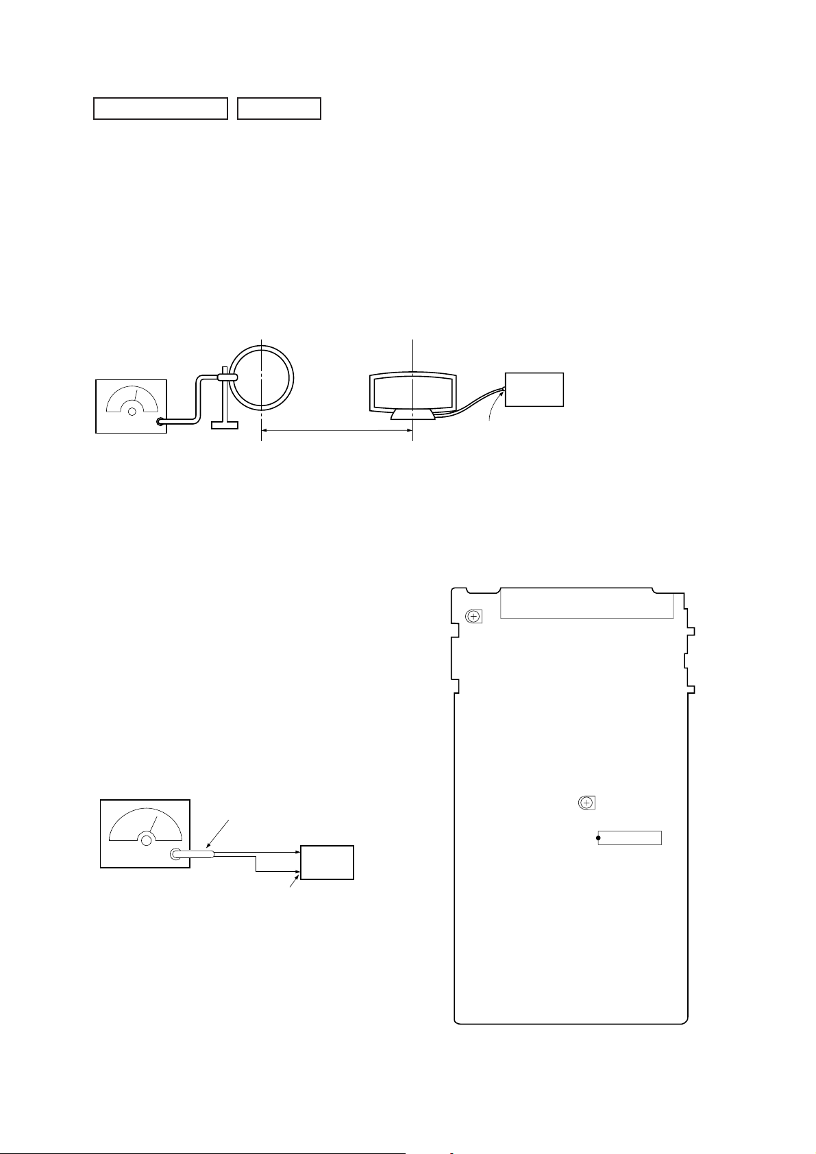
After correcting the original service problem, perform the following safety checks before releasing the set to the customer:
Check the antenna terminals, metal trim, “metallized” knobs, scre ws,
and all other exposed metal parts for A C leakage. Check leakage as
described below.
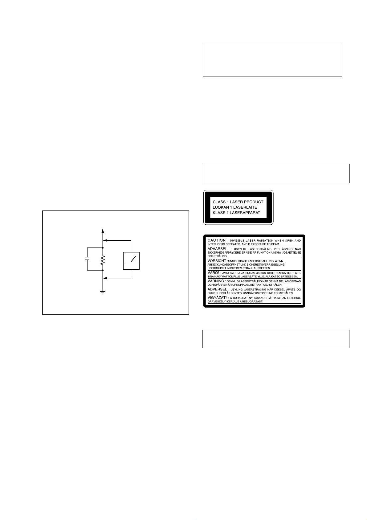
LEAKAGE
The AC leakage from any exposed metal part to earth Ground and
from all exposed metal parts to any exposed metal part having a
return to chassis, must not exceed 0.5 mA (500 microampers). Leakage current can be measured by any one of three methods.
1. A commercial leakage tester, such as the Simpson 229 or RCA
WT-540A. Follow the manufacturers’ instructions to use these
instruments.
2. A battery-operated AC milliammeter. The Data Precision 245
digital multimeter is suitable for this job.
3. Measuring the voltage drop across a resistor by means of a VOM
or battery-operated AC voltmeter. The “limit” indication is 0.75
V, so analog meters must have an accurate low-voltage scale.
The Simpson 250 and Sanwa SH-63Trd are examples of a passive VOM that is suitable. Nearly all battery operated digital
multimeters that have a 2V AC range are suitable. (See Fig. A)
To Exposed Metal
Parts on Set
CAUTION
Use of controls or adjustments or performance of procedures
other than those specified herein may result in hazardous radiation exposure.
Notes on chip component replacement
• Never reuse a disconnected chip component.
• Notice that the minus side of a tantalum capacitor may be
damaged by heat.
Flexible Circuit Board Repairing
• Keep the temperature of soldering iron around 270˚C
during repairing.
• Do not touch the soldering iron on the same conductor of the
circuit board (within 3 times).
• Be careful not to apply force on the conductor when soldering
or unsoldering.
Laser component in this product is capable of emitting radiation
exceeding the limit for Class 1.
This appliance is classified as
a CLASS 1 LASER product.
The CLASS 1 LASER PR ODUCT MARKING is located on
the rear exterior.
0.15µF
1.5k
Earth Ground
Ω
AC
voltmeter
(0.75V)
Fig. A. Using an AC voltmeter to check AC leakage.
SAFETY-RELATED COMPONENT WARNING !!
COMPONENTS IDENTIFIED BY MARK ! OR DOTTED LINE
WITH MARK ! ON THE SCHEMATIC DIAGRAMS AND IN
THE PARTS LIST ARE CRITICAL TO SAFE OPERATION.
REPLACE THESE COMPONENTS WITH SONY PARTS
WHOSE PART NUMBERS APPEAR AS SHOWN IN THIS
MANUAL OR IN SUPPLEMENTS PUBLISHED BY SONY.
The following
caution label is
located inside of
the unit.
NOTES ON HANDLING THE OPTICAL PICK-UP BLOCK
OR BASE UNIT
The laser diode in the optical pick-up block may suffer electrostatic
break-down because of the potential difference generated b y the
charged electrostatic load, etc. on clothing and the human body.
During repair, pay attention to electrostatic break-down and also
use the procedure in the printed matter which is included in the
repain parts.
The flexible board is easily damaged and should be handled with
care.
NOTES ON LASER DIODE EMISSION CHECK
ATTENTION AU COMPOSANT AYANT RAPPORT
À LA SÉCURITÉ!!
LES COMPOSANTS IDENTIFIÉS P AR UNE MARQUE ! SUR
LES DIAGRAMMES SCHÉMATIQUES ET LA LISTE DES
PIÈCES SONT CRITIQUES POUR LA SÉCURITÉ DE
FONCTIONNEMENT . NE REMPLACER CES COMPOSANTS
QUE PAR DES PIÈCES SONY DONT LES NUMÉROS
SONT DONNÉS DANS CE MANUEL OU DANS LES
SUPPLÉMENTS PUBLIÉS P AR SONY.
The laser beam on this model is concentrated so as to be focused on
the disc reflective surface b y the objective lens in the optical pickup block. Therefore, when checking the laser diode emission, observe from more than 30 cm away from the objective lens.
LASER DIODE AND FOCUS SEARCH OPERATION
CHECK
Carry out the “S curve check” in “CD section adjustment” and check
that the S curve waveform is output three times.
– 3 –

TABLE OF CONTENTS
1. GENERAL .......................................................................... 4
2. DISASSEMBLY
2-1. Front Panel ........................................................................... 6
2-2. Main Board ........................................................................... 6
2-3. Tape Mechanism Deck.......................................................... 7
2-4. Cassette Lid Assembly ..........................................................7
2-5. CD Lid Assembly.................................................................. 8
2-6. CD Mechanism Deck ............................................................ 8
2-7. Base Unit ..............................................................................8
2-8. Disc Table ............................................................................. 9
3. SERVICE MODE ............................................................ 10
4. MECHANICAL ADJUSTMENTS ..........................12
5. ELECTRICAL ADJUSTMENTS ............................... 12
6. DIAGRAMS
6-1. Circuit Boards Location ...................................................... 18
6-2. Brock Diagrams
• Tuner Section (AEP, UK model) ..................................... 19
• Tuner Section (East European, CIS model) ..................... 21
• CD Section ....................................................................... 23
• Deck Section .................................................................... 25
• Main Section .................................................................... 27
• Power Section ..................................................................29
6-3. Printed Wiring Board – CD Section –.................................33
6-4. Schematic Diagram – CD Section – ................................... 35
6-5. Schematic Diagram
– Tuner Section – (AEP, UK model)................................... 37
6-6. Printed Wiring Board
– Tuner Section – (AEP, UK model)................................... 39
6-7. Printed Wiring Board
– Tuner Section – (East European, CIS model) .................. 40
6-8. Schematic Diagram
– Tuner Section – (East European, CIS model) .................. 41
6-9. Printed Wiring Board – Main Section – .............................. 43
6-10. Schematic Diagram – Main (1/5) Section – ..................... 45
6-11. Schematic Diagram – Main (2/5) Section – ..................... 47
6-12. Schematic Diagram – Main (3/5) Section – ..................... 49
6-13. Schematic Diagram – Main (4/5) Section – ..................... 51
6-14. Schematic Diagram – Main (5/5) Section – ..................... 53
6-15. Printed Wiring Board – Deck Section – ........................... 55
6-16. Schematic Diagram – Deck Section – .............................. 57
6-17. Printed Wiring Board – Power Section – ......................... 59
6-18. Schematic Diagram – Power Section – ............................ 61
6-19. Schematic Diagram – Panel Section – ............................. 63
6-20. Printed Wiring Board – Panel Section –...........................65
6-21. Printed Wiring Board – TC/CD Panel-1 Section –...........67
6-22. Schematic Diagram – TC/CD Panel-1 Section – ............. 69
6-23. Schematic Diagram – HP/Mic Section – .......................... 71
6-24. Printed Wiring Board – HP/Mic Section – ....................... 73
6-25. Printed Wiring Board – CD Motor Section – ................... 75
6-26. Schematic Diagram – CD Motor Section – ...................... 77
6-27. Printed Wiring Board – Trans Section –........................... 79
6-28. Schematic Diagram – Trans Section – ............................. 81
6-29. Printed Wiring Board – Surround Section –..................... 83
6-30. Schematic Diagram – Surround Section – ....................... 84
6-31. IC Block Diagrams ........................................................... 85
6-32. IC Pin Functions ............................................................... 92
7. EXPLODED VIEWS
7-1. Case and Back Panel Section ............................................ 100
7-2. Front Panel Section 1 ........................................................ 101
7-3. Front Panel Section 2 ........................................................ 102
7-4. Chassis Section ................................................................. 103
7-5. TC Mechanism Section-1 (TCM-220WR2) ..................... 104
7-6. TC Mechanism Section-2 (TCM-220WR2) ..................... 105
7-7. TC Mechanism Section-3 (TCM-220WR2) ..................... 106
7-8. CD Mechanism Section
(CDM37L-5BD29AL/CMD37LH-5BD29AL) ................ 107
7-9. Base Unit Section (BU-5BD29AL) .................................. 108
8. ELECTRICAL PARTS LIST ...................................... 109
LOCATION OF PARTS AND CONTROLS
1 1/u button
2 REC button
3 t/CLOCK SET button
4 DAILY 1 button
5 DAILY 2 button
6 SLEEP button
7 DISPLAY/DEMO button
8 SPECTRUM ANALYZER button
9 Display Window
!º ENTER/NEXT button
!¡ TUNER MEMORY button
!™ TUNING MODE button
!£ TUNER/BAND button
!¢ TUNING (+/–) button
!∞ PTY button
(AEP, UK)
!§ STEREO/MONO button
!¶ Equalizer indicators
!• MIC LEVEL knob
!ª MIC jack
@º DSP button
@¡ WAVE button
@™ PROLOGIC button
@£ KARAOKE PON/MPX button
@¢ P FILE MEMORY button
@∞ PHONES jack
@§ EFFECT button
@¶ FUNCTION button
@• GROOVE button
@ª VOLUME control
#º SUPER WOOFER button
#º DBFB button (D890AV/XB55AV)
#¡ GEQ control buttons
#™ GEQ CONTROL button
#£ SUPER W MODE button
#¢ ENTER button
#∞ Deck A ª, · button
#§ Deck A p button
#¶ DIRECTION button
#• DOLBY NR button
#ª Deck A 0, ) button
$º Deck A 6 EJECT button
$¡ Deck B p button
$™ Deck B ª, · button
SECTION 1
GENERAL
(XB80AV/XB88AV)
(XB80AV/XB88AV)
$£ Deck B 0, ) button
$¢ Deck B r REC button
$∞ Deck B P button
$§ CD SYNC button
$¶ H SPEED DUB button
$• Deck B 6 EJECT button
$ª 6 OPEN button
%º CD · button
%¡ CD p button
%™ CD P button
%£ DISC SKIP button
%¢ DISC1-DISC5 buttons
%∞ NON-STOP button
%§ LOOP button
%¶ FLASH button
%• 1/ALL DISCS button
%ª PLAY MODE button
^º CD 0, ) button
^¡ REPEAT button
^™ EDIT button
^£ ≠ AMS ± dial
– 4 –
Front Panel
2
3
4
5
6
!•
!ª
@¡
@∞
#∞
#§
178
!¶
@º @™@£ @¢
9!º!¡ !£
@§
#¢ #™
#¡
!™
@•
!∞
!§
!¢
@¶
@ª
#º
#£
$™
$£
#¶
#•
$º
%¢
%∞
%§
#ª
$¡ $¶
$¢
$∞
$§
$•
$ª
%º
%¡
%™
%£
^º
%ª%•
^¡
%¶
^™ ^£
– 5 –

SECTION 2
)
DISASSEMBLY
Note: Follow the disassembly procedure in the numerical order given.
2-1. FRONT PANEL
1
Three flat type wiers
(CN401,CN402,CN701)
3
Front panel
2-2. MAIN BOARD
3
Power cord
2
Four screws (BVTP3x8)
4
Back panel
2
Eleven screws (BVTP3x8)
1
Flat type wire (CN1)
9
Main board
!º
Connector (CN961
5
Flat type wire (CN801)
– 6 –
8
Connector (CN901)
7
Two screws (BVTP3x8)
6
Connector (CN830)

2-3. TAPE MECHANISM DECK
3
Three screws (BVTP2.6x8)
A
Three screws (BVTP2.6x8)
4
5
Remove the tape mechanism deck
section to direction of arrow
A
.
2
Open the cassette lid.
2-4. CASSETTE LID ASSEMBLY
1
Two springs.
1
Push the two buttons.
3
Two brackets.
2
Two screws (BVTP2.6x8)
4
Cassette lid assembly
– 7 –
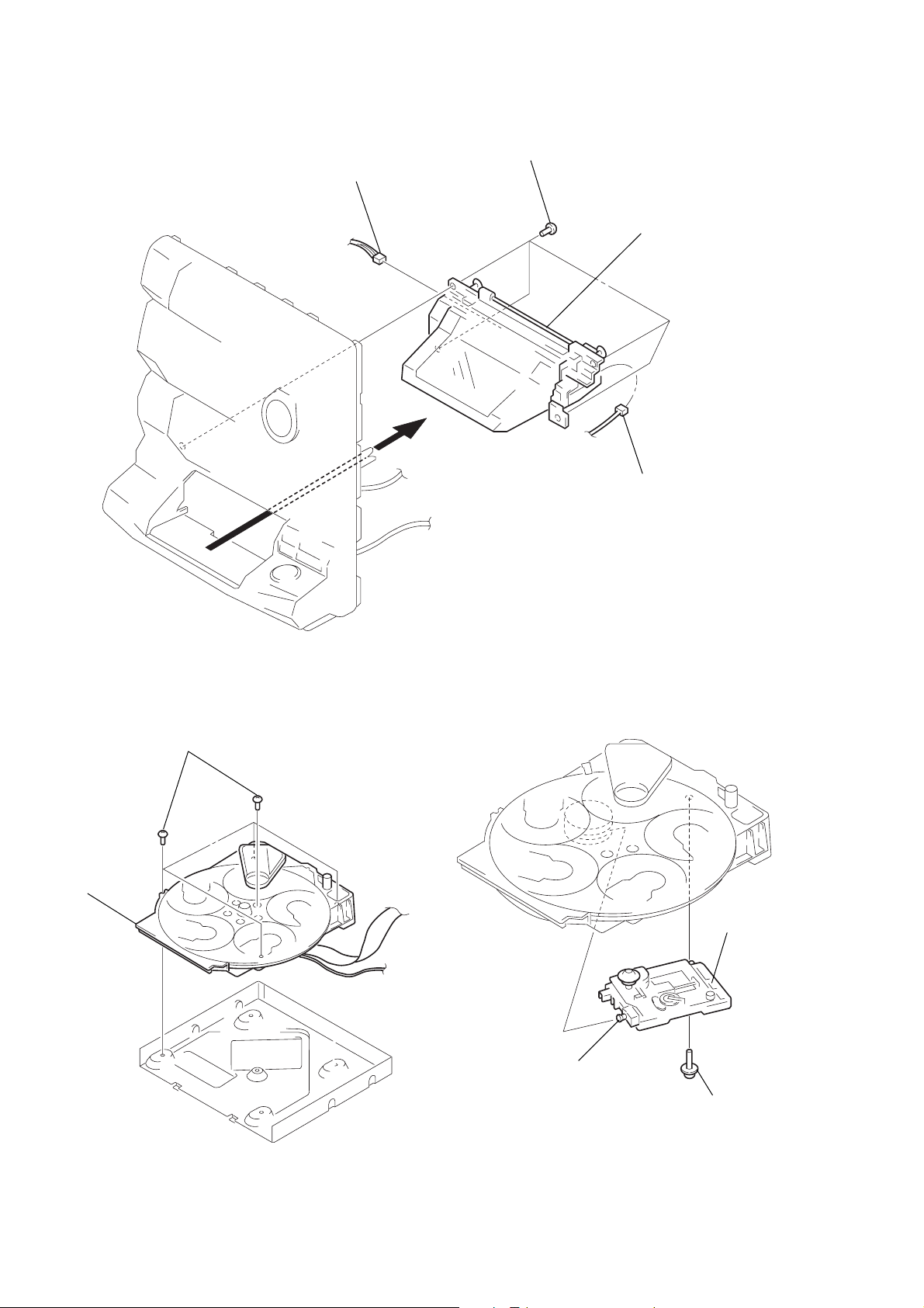
2-5. CD LID ASSEMBLY
)
t
2
Connector (CN671)
1
Four screws (BVTP2.6x8)
4
3
CD lid assembly
Connector (CN661
2-6. CD MECHANISM DECK
1
Five screws (BVTP3x8)
2
CD mechanism
deck
2-7. BASE UNIT
2
Boss
3
Base unit
1
Yoke bracke
– 8 –

2-8. DISC TABLE
e
NOTE:
When the disc table is installed, adjust the positions of
roller cam and mark ” as shown in the figure, then set to
the groove of disc table.
A
2
Screw (BVTP3X8)
3
Bracket (BU)
1
Screw (BVTP3X8)
4
Stop screw
5
Disc tabl
A
– 9 –

SECTION 3
SERVICE MODE
MC Cold Reset
• The cold reset clears all data including preset data stored in the RAM to initial conditions. Execute this mode when returning the set to the
customer.
Procedure:
1. Press three buttons SPECTRUM ANALYZER , ENTER , and DISC 1 simultaneously.
2. The fluorescent indicator tube becomes blank instantaneously, and the set is reset.
CD Delivery Mode
• This mode moves the pick-up to the position durable to vibration. Use this mode when returning the set to the customer after repair.
Procedure:
1. Press 1/u button to turn the set ON.
2. Press PLAY MODE button and 1/u button simultaneously.
3. A message “LOCK” is displayed on the fluorescent indicator tube, and the CD delivery mode is set.
MC Hot Reset
• This mode resets the set with the preset data kept stored in the memory. The hot reset mode functions same as if the power cord is plugged
in and out.
Procedure:
1. Press three buttons SPECTRUM ANALYZER , ENTER , and DISC 2 simultaneously.
2. The fluorescent indicator tube becomes blank instantaneously, and the set is reset.
Sled Servo Mode
• This mode can run the CD sled motor freely. Use this mode, for instance, when cleaning the pick-up.
Procedure:
1. Select the function “CD”.
2. Press three buttons SPECTRUM ANALYZER , ENTER , and FUNCTION simultaneously.
3. The Sled Servo mode is selected, if “CD” is blanking on the fluorescent indicator tube.
4. With the CD in stop status, press ) button in CD section to move the pick-up to outside track, or 0 button to inside track.
5. To exit from this mode, perform as follows:
1) Move the pick-up to the most inside track.
2) Press three buttons in the same manner as step 2.
Note:
• Always move the pick-up to most inside track when exiting from this mode. Otherwise, a disc will not be unloaded.
• Do not run the sled motor excessively, otherwise the gear can be chipped.
Change-over of FUNCTION Name
• The FUNCTION name of external input terminal can be changed over to VIDEO or MD. With the FUNCTION selected to “MD”, about
5dB mute is applied to the input gain.
Procedure:
1. Press 1/u button to turn the set OFF.
2. Press 1/u button together with FUNCTION button, and the power is turned on, the display of fluorescent indicator tube changes to
“MD” or “VIDEO” instantaneously, and thus the FUNCTION is changed over.
Change-over of AM Tuner Step between 9kHz and 10kHz
• A step of AM channels can be changed over between 9kHz and 10kHz.
Procedure:
1. Press 1/u button to turn the set ON.
2. Select the function “TUNER”, and press TUNER/BAND button to select the BAND “AM”.
3. Press 1/u button to turn the set OFF.
4. Press ENTER/NEXT and 1/u buttons simultaneously, and the display of fluorescent indicator tube changes to “AM 9k STEP” or “AM
10k STEP”, and thus the channel step is changed over.
LED and Fluorescent Indicator Tube All Lit, Key Check Mode
Procedure:
1. Press three buttons SPECTRUM ANALYZER , ENTER , and DISC 3 simultaneously.
2. LEDs and fluorescent indicator tube are all turned on.
Press DISC 2 button, and the key check mode is activated.
3. In the key check mode, the fluorescent indicator tube displays “K 1 V0 J0”. Each time a button is pressed, “K”value increases. Howe ver,
once a button is pressed, it is no longer taken into account.
“J” Value increases like 1, 2, 3 ... if rotating JOG knob in “+” direction, or it decreases like 0, 9, 8 ... if rotating in “-” direction.
“V” Value increases like 1, 2, 3 ... if rotating VOLUME knob in “+” direction, or it decreases like 0, 9, 8 ... if rotating in “-” direction.
4. To exit from this mode, press three buttons in the same manner as step 1, or disconnect the power cord.
– 10 –

Aging Mode
This mode can be used for operation check of CD section and tape deck section.
• If an error occurred:
The aging operation stops.
• If no error occurs:
The aging operation continues repeatedly.
1. Aging Mode in CD Section
1-1. Operating procedure of Aging Mode
1. Set discs in DISC 1 and DISC 3 trays.
2. Select the function “CD”.
3. Press three buttons SPECTRUM ANALYZER , ENTER , and KARAOKE PON/MPX simultaneously.
4. The aging mode is activated, if a roulette mark on the fluorescent indicator tube is blinking.
5. In the aging mode, the aging is executed in a sequence given in “1-2. Operation during Aging Mode”.
The aging continues unless an alarm occurred.
6. To exit from the aging mode, press 1/u button to turn the set OFF.
• If a button other than buttons In CD section is pressed during aging, the aging in the CD section is finished.
• To execute aging to the tape deck section successively, press · button in the deck A.
“AGING” is displayed on the fluorescent indicator tube. (For the aging in tape deck, see “2. Aging Mode in Tape Deck Section”.
1-2. Operation during aging Mode
In the aging mode, the program is executed in the following sequence.
1. The disc tray turns to select a disc. (For a disc selection sequence, see Section 1-3.)
2. TOC of disc is read.
3. The pick-up accesses to the last track.
4. Steps 1 through 3 are repeated.
1-3. Disc Selection Sequence
• During the aging mode, discs are selected in the following sequence:
Disc 1 → Disc 3
↑↓
Disc 3 ← Disc 1
2. Aging Mode in Tape Deck Section
2-1. Operating procedure of Aging Mode
1. Load a commercially available 10-minute tape into the decks A and B respectively.
(If a 10-minute tape is not available, another tape may be used but a cycle time will be longer.)
2. Select the function “TAPE”.
3. Rewind tapes in advance by pressing 0 button respectively on decks A and B.
4. Press three buttons SPECTRUM ANALYZER , ENTER , and KARAOKE PON/MPX simultaneously.
5. Press · button on deck A. (This button triggers the aging mode.)
6. The aging mode is activated if “AGING A” is displayed on the fluorescent indicator tube.
7. In the aging mode, the aging is executed in a sequence given in “2-2. Operation during Aging Mode”.
The aging continues unless an alarm occurred.
8. To exit from the aging mode, press 1/u button to turn the set OFF.
2-2. Operation during Aging Mode
In the aging mode, the program is executed in the following sequence.
1. A tape on FWD side is played for one minute.
2. PAUSE STOP is made.
3. Recording is made for 3 minutes. (For the deck not having the record function, the play is executed.)
4. FF is executed up to the end of tape.
5. A tape is reversed, and the tape on REV side is played for one minute.
6. PAUSE STOP is made.
7. Recording is made for 3 minutes. (For the deck not having the record function, the play is executed.)
8. FF is executed up to the end of tape.
9. Steps 1 through 8 are executed for the other deck.
10. Steps 1 through 9 are repeated unless an alarm occurred.
2-3. Deck Selection Sequence
• During the aging mode, decks are selected in the following sequence:
Deck A (FWD) → Deck A (REV)
↑↓
Deck B (REV) ← Deck B (FWD)
– 11 –

SECTION 4
)
MECHANICAL ADJUSTMENTS
SECTION 5
ELECTRICAL ADJUSTMENTS
Precaution
1. Clean the f ollowing parts with a denatured alcohol-moistened
swab:
record/playback heads pinch rollers
erase head rubber belts
capstan idlers
2. Demagnetize the record/playback head with a head demagnetizer.
3. Do not use a magnetized screwdriver for the adjustments.
4. After the adjustments, apply suitable locking compound to the
parts adjusted.
5. The adjustments should be performed with the rated power supply voltage unless otherwise noted.
Torque Measurement
Mode
FWD
FWD
back tension
REV
REV
back tension
FF/REW
FWD tension
REV tension
Torque meter
CQ-102C
CQ-102C
CQ-102RC
CQ-102RC
CQ-201B
CQ-403A
CQ-403R
Meter reading
36 to 61 g • cm
(0.5 - 0.84 oz • inch)
2 to 6 g • cm
(0.02 - 0.08 oz • inch)
36 to 61 g • cm
(0.5 - 0.84 oz • inch)
2 to 6 g • cm
(0.02 - 0.08 oz • inch)
61 to 143 g • cm
(0.85 - 1.99 oz • inch)
100 g or more
(3.53 oz or more)
100 g or more
(3.53 oz or more)
DECK SECTION 0 dB=0.775V
1. Demagnetize the record/playback head with a head damagnetizer .
2. Do not use a magnetized screwdriver for the adjustments.
3. After the adjustments, apply suitable locking compound to the
parts adjusted.
4. The adjustments should be performed with the rated power supply voltage unless otherwise noted.
5. The adjustments should be performed in the order given in this
service manual. (As a general rule, playback circuit adjustment
should be completed before performing recording circuit adjustment.)
6. The adjustments should be performed for both L-CH and R-CH.
7. Switches and controls should be set as follows unless otherwise
specified.
Signal
P-4-A100
WS-48B
P-4-L300
10 kHz, –10 dB
3 kHz, 0 dB
315 Hz, 0 dB
Record/Playback Head Azimuth Adjustment
(Deck A, Deck B)
Note: Perform this adjustments for both decks.
Procedure:
1. Mode : Playback
test tape
P-4-A100
(10kHz, –10dB)
main board
CN403
Pin
3
(L-CH)
Pin
1
(R-CH)
Used forTape
Azimuth Adjustment
Tape Speed Adjustment
Level Adjustment
level meter
set
main board
CN403
Pin
2
(GND
– 12 –

2. Turn the adjustment screw and check output peaks. If the peaks
do not match for L-CH and R-CH, turn the adjustment screw
so
that outputs match within 1 dB of peak.
L-CH
peak
output
level
within
1 dB
within 1dB
Tape Speed Adjustment (Deck A)
Note: Set the test mode using the following method and begin tape
speed adjustment.
In the test mode, the tape will move at double speed or normal
speed each time the H SPEED DUB. button is pressed.
Procedure :
With the power tur ned ON, press the SPECTRUM ANALYZER
button, ENTER button, and EFFECT button simultaneously.
(The “VOLUME” on the fluorescent display tube will blink while
in the test mode.)
To exit the test mode, press the 1/u button.
R-CH
screw
position
peak
L-CH
peak
R-CH
peak
screw
position
3. Mode: Playback
test tape
P-4-A100
(10kHz, –10dB)
in phase 45
main board
CN403
Pin
3
(L-CH)
Pin 2 (GND)
L
set
R
Pin
1
(R-CH)
Waveform of oscilloscope
°
90
°
good
135
oscilloscope
°
wrong
180
°
4. After the adjustments, apply suitable locking compound to the
parts adjusted.
Adjustment Location: Playback Head (Deck A)
Record/Playback/Erase Head (Deck B)
1. Load WS-48B into deck B.
2. Play deck B.
3. Press the H SPEED DUB. button and play the tape at double
speed.
4. Adjust RV652 of the AUDIO board so that the reading of the
frequency counter becomes 6000 ± 180 Hz.
5. Press the H SPEED DUB. button and play the tape at normal
speed.
6. Adjust RV651 of the AUDIO board so that the reading of the
frequency counter becomes 3000 ± 90 Hz.
Adjustment Location: A UDIO board
Sample Value of Wow and flutter
W.RMS (JIS) less than 0.3%
(test tape: WS-48B)
Playback Level Adjustment (Deck A, Deck B)
Procedure:
Mode: Playback
test tape
P-4-L300
(315Hz, 0dB)
set
main board
CN403 Pin
Pin
3
1
level meter
(L-CH)
(R-CH)
Deck A is RV311 (L-CH) and RV411 (R-CH), deck B is RV301
(L-CH) and RV401 (R-CH)
so that adjustment within the following adjustment level.
forward
Adjustment level:
CN403 playback level: 301.5 to 338.3 mV (–8.2 to –7.2 dB)
level difference between the channels: within ± 0.5 dB
Adjustment Location: A UDIO board
reverse
– 13 –
Record Bias Adjustment (Deck B)
Record Level Adjustment (Deck B)
Procedure:
INTRODUCTION
When set to the test mode performed in Tape Speed Adjustment, when the ta pe is rewound after recording, the “REC memory
mode” which rewinds only the recorded portion and playback is
set.
This “REC memory mode” is convenient for performing this adjustment. During recording, the input signal FUNCTION will automatically switch to VIDEO.
1. Press FUNCTION button to select VIDEO. (This step is not
necessary if the above test mode has already been set.)
2. Load a tape into deck B, and press the r REC button.
3. Mode: Record
VIDEO/MD (AUDIO) IN
1) 315 Hz
2) 10 kHz
AF OSC
attenuator
600
Ω
} 50 mV (–23.8 dB)
blank tape
CS-123
set
4. Mode: Playback
Procedure:
INTRODUCTION
When set to the test mode performed in Tape Speed Adjustment, when the tape is rewound after recording, the “REC memory
mode” which rewinds only the recorded portion and playback is
set.
This “REC memory mode” is convenient for performing this
adjustment. During recording, the input signal FUNCTION will automatically switch to VIDEO.
1. Press FUNCTION button to select VIDEO. (This step is not
necessary if the above test mode has already been set.)
2. Load a tape into deck B, and press the r REC button.
3. Mode: Record
VIDEO/MD (AUDIO) IN
1) 315 Hz
2) 10 kHz
AF OSC
attenuator
} 50 mV (–23.8 dB)
600
Ω
blank tape
CS-123
set
4. Mode: Playback
recorded
position
set
main board
CN403 Pin
Pin
3
1
level meter
(L-CH)
(R-CH)
5. Confirm playback the signal recorded in step 2 become adjustment level as follows.
If these levels do not adjustment le vel, adjust the R V341 (L-CH)
and R V441 (R-CH) on the A UDIO board to repeat steps 3 and 4.
Adjustment level: The playback output of 10 kHz le vel difference
against 315 Hz reference should be ± 1.0 dB.
Adjustment Location: A UDIO board
Adjustment Location
[AUDIO BOARD] (Conductor Side)
RV341(Lch),RV441(Rch)
Record Bias
RV301
RV401
RV301(Lch),RV401(Rch)
Playback Level (Deck B)
RV441
RV341
RV651 (Normal Speed)
RV652 (High Speed)
Tape Speed
RV311(Lch),RV411(Rch)
Playback Level (Deck A)
RV651
RV311
RV411
RV652
recorded
position
set
main board
CN403 Pin
Pin
3
1
level meter
(L-CH)
(R-CH)
5. Confirm playback the signal recorded in step 2 become adjustment level as follows.
If these levels do not adjustment level, adjust the R V301 (L-CH)
and RV351 (R-CH) on the MAIN board to repeat steps 3 and 4.
Adjustment level:
CN403 playback level: 47.2 to 53.0 mV (–24.3 to –23.3 dB)
Adjustment Location: MAIN board
RV301
[MAIN BOARD] (Component Side)
Record Level (L CH)
1
CN403
IC401
3
RV351
Record Level
(R CH)
– 14 –
TUNER SECTION 0dB=1µV
Note 1: As a front-end (FE1) is difficult to repair if faulty , replace
it with new one.
Note 2: No adjustment is needed due to a tuner pack for except
AEP, UK, East European, CIS models.
AM Tuned Level Adjustment
(AEP, UK, East European, CIS model only)
Note: FM Tuned Level adjustment should be performed after this
AM Tuned Level Adjustment.
Setting:
Band: MW
AM RF SSG
30% amplitude
modulation by
400Hz signal
Modulation: 999 kHz
loop antenna
60cm
Field strength dB (
loop antenna
(Supplied accessories)
µ
V/m) = SSG output level dB (µV/m) –26dB.
set
AM antenna
terminal (TM1)
Procedure:
1. Set the output of SSG so that the input level of the set becomes
55 dB.
2. Tune the set to 999 kHz.
3. Adjust R V41 to the point (moment) when the TUNED indicator
will change from going off to going on.
Adjustment Location: TCB board
FM Tuned Level Adjustment
(AEP, UK, East European, CIS model only)
Note: This adjustment should be performed after the AM Tuned
Level Adjustment.
Setting:
Band: FM
FM RF SSG
75
Ω
coaxial
set
Carrier frequency: 98MHz
Modulation: AUDIO 1kHz, 75kHz
Output level: 25dB (at 75
deviation (100%)
Ω
FM ANTENNA terminal (TM1)
open)
Adjustment Location
[TCB BOARD] (Component Side)
TM1
RV41
AM Tuner Level
RV42
FM Tuned
Level
IC21
Procedure:
1. Supply a 25 dB 98 MHz signal from the ANTENNA terminal.
2. Tune the set to 98 MHz.
3. Adjust RV42 to the point (moment) when the TUNED indicator
will change from going off to going on.
Adjustment Location: TCB board
– 15 –
FM Polar Adjustment (East European, CIS model only)
Connection 1 :
FM RF SSG
Carrier frequency: 69 MHz
Output level: 1 mV (60 dB
Modulation: AUDIO 1 kHz, 10 kHz deviation
75
Ω
coaxial
FM antenna
terminal (75
set
Ω
)
µ
) (at 75 Ω open)
Connection 2 :
AF OSC
FM RF SSG
75
Ω
coaxial
set
Procedure :
1. Set the modulation of FM RF SSG to AUDIO 1 kHz, 10 kHz
deviation according to “Connection 1”.
2. Tune the set to 69 MHz.
3. Adjust the R V1702 so that the reading of frequency counter connected to TP1702 (VCO) becomes within 31.25 kHz ± 0.05 kHz.
(VCO adjustment)
4. Then record the reading of the level meter connected to TP1701.
5. Set the modulation of FM RF SSG to AUDIO 31.25 kHz, 10
kHz deviation according to “Connection 2”.
6. Tune the set to 69 MHz.
7. Set the CT1701 to be mechanical center.
8. Adjust the L1701 so that the reading of the level meter connected to TP1701 (FILTER) becomes maximum.
Then adjust the CT1701 so that the reading of the level meter
connected to TP1701 (FIL TER) becomes maximum. (SUB CARRIER PEAK Adjustment)
9. Adjust the RV1701 so that the level at the moment becomes 14
dB higher value than the level recorded in step 4. (SUB CARRIER LEVEL Adjustment)
Audio 31.25 kHz
Carrier frequency: 69 MHz
Output level: 1 mV (60 dB
Modulation: AUDIO 31.25 kHz, 10 kHz deviation
external
modulation
terminal
µ
) (at 75 Ω open)
(EXTERNAL MODULATION)
Adjustment Location: TCB board
Adjustment Location:
[TCB BOARD] (Conductor Side)
frequency counter
TP1701
(FILTER)
level meter
TP1702
(VCO)
FM antenna
terminal (75
IC1701
Ω
)
[TCB BOARD] (Component Side)
L1701
CT1701
RV1701
Sub Carrier
Level
IC1701
RV1702
VCO
Sub Carrier Peak
– 16 –

CD SECTION
Note:
1. CD Block is basically constructed to operate without adjustment.
Therefore, check each item in order given.
2. Use YEDS-18 disc (3-702-101-01) unless otherwise indicated.
3. Use an oscilloscope with more than 10MΩ impedance.
4. Clean the object lens by an applicator with neutral detergent when
the signal level is low than specified value with the following
checks.
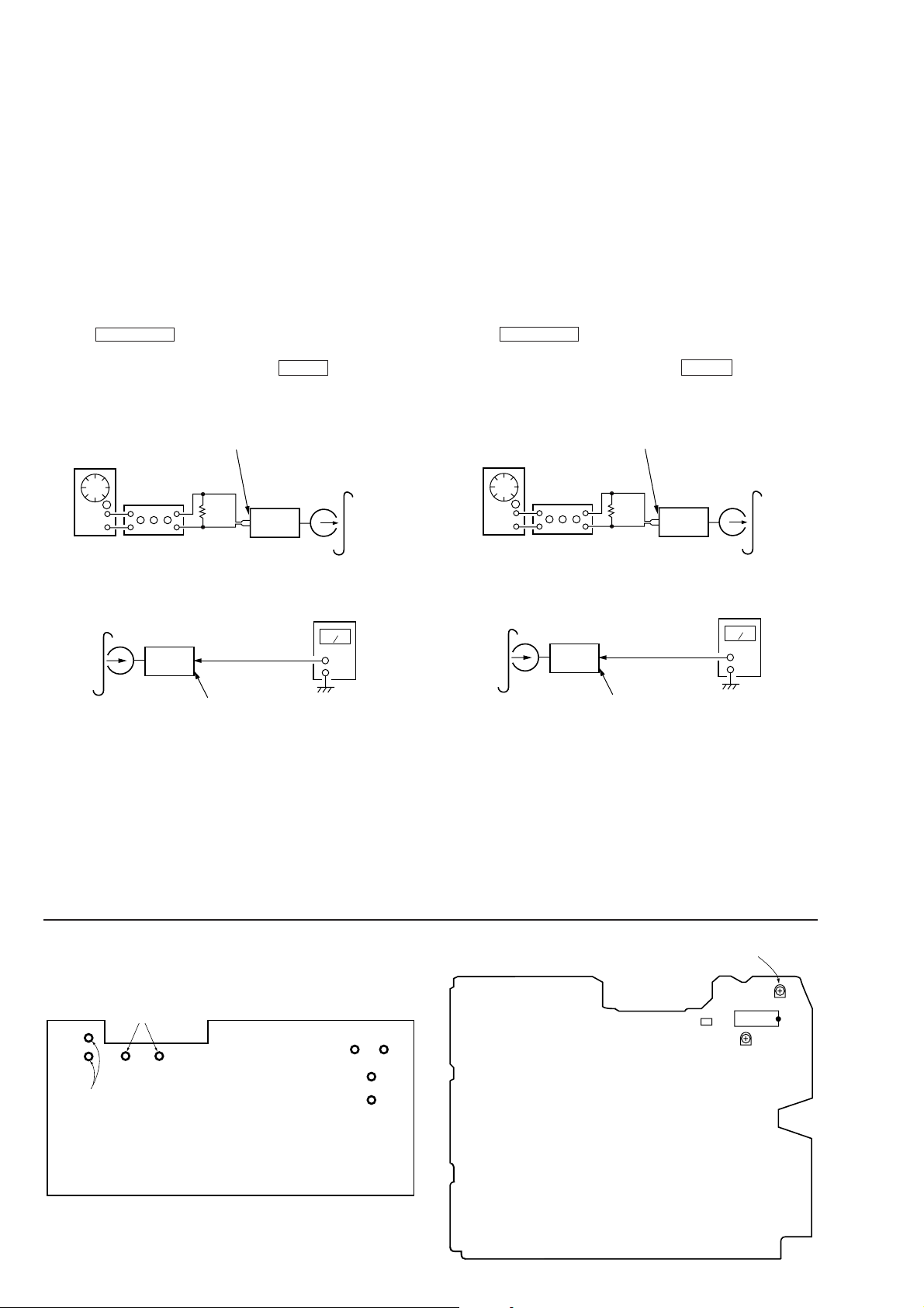
S Curve Check
oscilloscope
BD board
TP (FEO)
TP (VC)
Procedure :
1. Connect oscilloscope to test point TP (FEO).
2. Connect between test point TP (FOK) and Ground by lead wire.
3. Turn Power switch on.
4. Put disc (YEDS-18) in and turned Power switch on again and
actuate the focus search. (actuate the focus search when disc
table is moving in and out.)
5. Check the oscilloscope waveform (S-curve) is symmetrical between A and B. And conf irm peak to peak level within 3 ± 1Vp-p.
E-F Balance (1 Track Jump) check
oscilloscope
BD board
TP (TEO)
TP (VC)
Procedure:
1. Connect oscilloscope to test point TP (TEO) on BD board.
2. Turned Power switch on.
3. Put disc (YEDS-18) in to play the number five track.
4. Press the “P (Pause)” button.
5. Check the level B of the oscilloscope's wav eform and the A (DC
voltage) of the center of the Traverse waveform.
Confirm the following:
• A/B x 100 = less then ± 7 (%)
• B = 500 ± 100 mVp-p
1 track jump waveform
Center of the waveform
B
A (DC voitage)
0V
S-curve waveform
symmetry
A
Within 3
±
1 Vp-p
B
6. After check, remove the lead wire connected in step 2.
Note: • Try to measure sev eral times to make sure than the ratio of
A : B or B : A is more than 10 : 7.
• Take sweep time as long as possible and light up the brightness to obtain best waveform.
RF Level Check
oscilloscope
BD board
TP (RF)
TP (VC)
Procedure :
1. Connect oscilloscope to test point TP (RF) on BD board.
2. Turned Power switch on.
3. Put disc (YEDS-18) in and playback.
4. Confirm that oscilloscope waveform is clear and check RF signal level is correct or not.
Note: Clear RF signal waveform means that the shape “◊” can be
clearly distinguished at the center of the waveform.
level : 500 mV
±
100 mVp-p
Adjustment Location:
[BD BOARD] (Conductor Side)
TP (RF)
IC101
CN101
TP
(TEO)
TP
(FEO)
TP
(GND)
IC103
IC102
TP
(VC)
TP
(FOK)
IC102
Symmetry
RF signal waveform
VOLT/DIV : 200mV
TIME/DIV : 500ns
level : 1.3
±
0.3 Vp-p
– 17 –

6-1. CIRCUIT BOARDS LOCATION
d
)
PANEL board
SECTION 6
DIAGRAMS
TRANS board
ENCAPSULATED COMPONENT(D890AV/XB55AV/XB88AV
TCB board(XB80AV)
HP/MIC board
TC-A SW board
CD-LED board
CD-A SW board
DOOR SW board
TC-B SW board
CD-B2 SW board
Note: pA is including in AUDIO board.
POWER board
CD-B1 SW board
p
A
MOTOR board
SURROUND board
MAIN board
TABLE SENSOR board
CD MOTOR board
AUDIO board
(including
p
A)
LEAF SWITCH boar
BD board
LED board
– 18 –

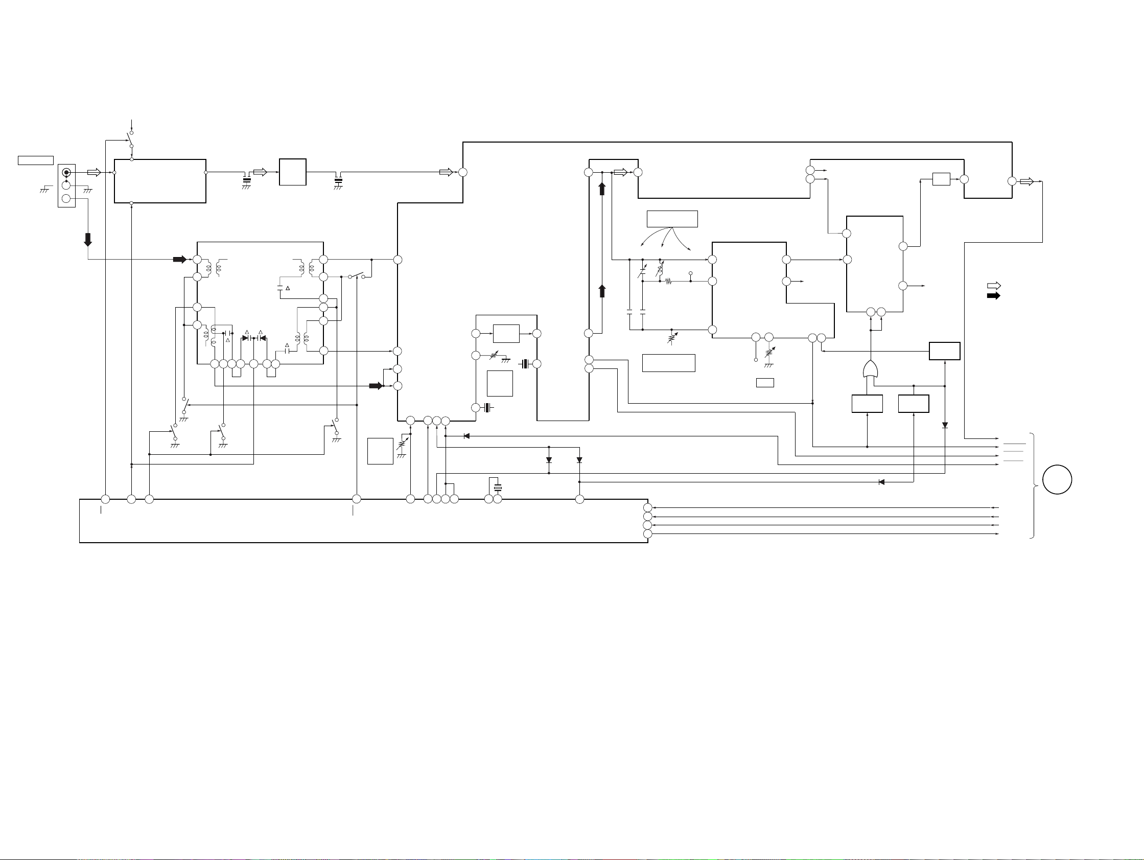
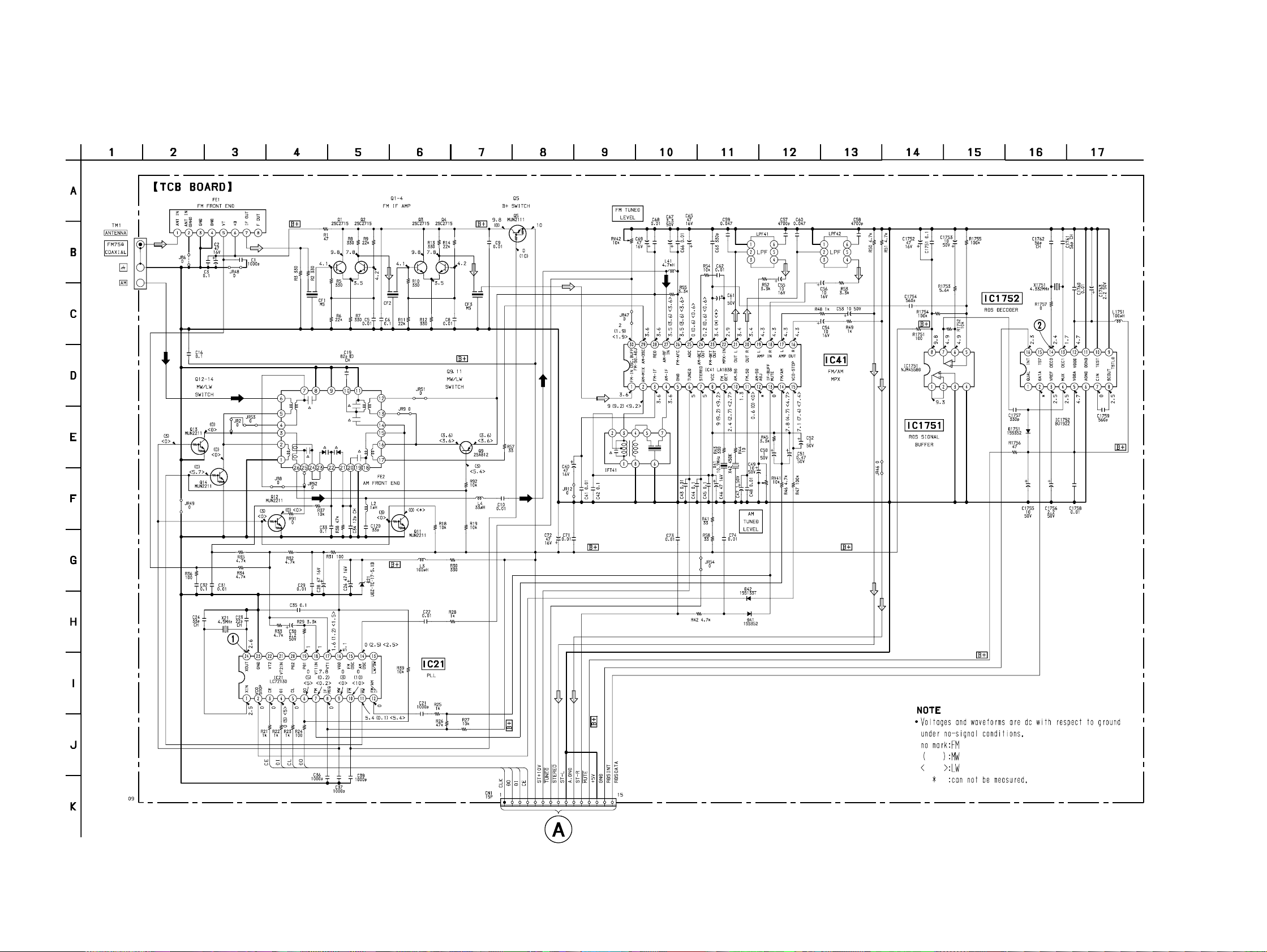
6-2. BLOCK DIAGRAMS
– TUNER SECTION – (AEP, UK model)
ST +10V
HCD-D890AV/XB55AV/XB80AV/XB88AV
TM1
ANTENNA
FM 75Ω
COAXIAL
AM
Q5
ANT IN
VT
FE1
FM FRONT END
IF OUT
Q13
MW
SW
6
5
3
2
26 25 24 23 22 21
Q14
LW SW
CF1
10.7MHz
FE2
MW/LW FRONTEND
Q12
MW
SW
28
29
26
27
10.7MHz
REG
AM OSC
FM AFC
AM RF IN
FM SD
OSC.BUFF
30 14
CF3
ADJ
VCO STOP
AM/FM
15
13
AM MIX
ADJ
MUTE
IF BUFF
1 FM IN
FM/AM MPX
IC41
2
AM
12
SD
AM
10
SD
450kHz
D41
RV41
X42
AM IF
AM
TUNED
LEVEL
IFT41
X41
10.7MHz
4
9
FM DET OUT
AM IF
FM
DET
23 22
AM
24
DET
OUT
7
STEREO
6
TUNED
OUT L
MPX IN
OUT R
IC1751
57
4
ST L
RDS INT
RDS DATA
STEREO
TUNED
MUTE
21
LPF
RCH
20
RDS DECODER
IC1752
13 14
X1751
4.332MHz
A
MAIN
SECTION
AMP IN L
AMP
OUT
17
L
19
2
16
• R CH: Same as L ch
• SIGNAL PATH
: FM
: MW
CF2
IF AMP
Q1, 2
20
10.7MHz
12
13
14
15
16
17
LW SW
Q11
MW
SW
IF AMP
Q3, 4
Q9
RV42
FM
TUNED
LEVEL
(Page 27)
X21
2
AM OSC
7
FM
1214
FM/AM IF
VCO STOP
1710
9
FM
VT1
MW
09
PLL
IC21
11
MW
1 24
XIN
XOUT
4.5MHz
3 ST-CE
CE
4
DI
5
CL
DO
6
COM-DIN
COM-CLK
COM-DATA
– 19 – – 20 –
HCD-D890AV/XB55AV/XB80AV/XB88AV
– TUNER SECTION – (East European, CIS model)
ST +10V
TM1
ANTENNA
FM 75Ω
COAXIAL
AM
ANT IN
Q5
VT
FE1
FM FRONT END
IF OUT
LW SW
Q13
MW
SW
6
5
3
2
26 25 24 23 22 21
Q14
CF1
10.7MHz
FE2
MW/LW FRONTEND
Q12
MW
SW
CF3
IF AMP
Q1-4
20
10.7MHz
12
13
14
15
16
17
LW SW
Q11
MW
SW
20
21
R CH
VCO
ST IND
910
RCH
STOP
POLAR/PILOT
12
L IN
POLA
13
L IN
SWITCH
IC1702
CA
9 11
SWITCH
Q1702
L OUT
R OUT
D1701
D1702
14
4
SWITCH
Q1703
R CH
D1703
LPF 19
SWITCH
Q1701
AMP
AMP
IN
L
OUT
17
L
• R CH: Same as L ch
• SIGNAL PATH
: FM
: MW
ST-L
STEREO
TUNED
MUTE
L OUT
R OUT
MON
VCO
OUT R
OUT L
7
6
VCO
RV1702
MPX IN
1 FM IN
FM/AM MPX
IC41
28
REG
Q9
AM IF
2
RV42
FM
TUNED
LEVEL
29
26
27
AM OSC
FM AFC
AM RF IN
FM SD
ADJ
OSC.BUFF
30 14
AM/FM
15
AM MIX
MUTE
IF BUFF
VCO STOP
13
AM
SD
ADJ
AM
SD
D41
12
10
RV41
X42
450kHz
IFT41
AM
TUNED
LEVEL
X41
10.7MHz
4
9
FM DET OUT
AM IF
FM
DET
23
AM
24
DET
OUT
STEREO
7
TUNED
6
D42 D43
22
SUB CARRIER
PEAK
L1701CT1701
RV1701
SUB CARRIER
LEVEL
TP1701
POLAR
DECODER
IC1701
2
IN
3
POUT
SUB IN
20
18 17
TP1702
X21
2
AM OSC
7
FM
1214
8
IF REQ
FM/AM IF
VCO STOP
1710
9
FM
VT1
MW
09
PLL
IC21
11
MW
1 24
XIN
XOUT
4.5MHz
13
FM LOW
3
CE
4
DI
5
CL
6
DO
D1704
ST-CE
COM-DIN
COM-CLK
COM-DATA
A
MAIN
SECTION
(Page 27)
– 21 – – 22 –

– CD SECTION –
OPTICAL PICK-UP BLOCK
K
E
A
B
LASER
DIODE
DETECTOR
HCD-D890AV/XB55AV/XB80AV/XB88AV
IC391
1
D.OUT
FOCUS/TRACKING SERVO.
RF AMP
38
39
41
42
2
1
45
47
3637LD
IC101 (1/2)
PD1
PD2
F
E
FEI
FEO
TEO
TEI
PD
SENS1
SENS2
XRST
23
RF O
LOCK
C.OUT
FE O
FE M
TA M
TA O
DATA
XLT
CLK
FOK
33
19
24
25
26
6
7
12
13
22
21
20
27
RF
44
LOCK
29
14
CNIN
15
SEIN
B+
A
D
D
C
C
B
F
1
4
2
5
10
6
LD DRIVE
Q101
DATAO
XLTO
15 16 17
71
CLKO
DOUT
27
MDP
FOK
23
SPOD
21
CD DIGITAL
OUT
OPTICAL
DIGITAL SIGNAL PROCESSOR
IC103
DATA
10 11 12 75
S101
LIMIT
XLAT
CLOK
SQCK
SENS
SCOR
SQSO
8
79 100
XRST
89 • 90
XTAI
LOUT1
LOUT2
16.9344MHz
•
XTAO
X101
86
93
L-CH
R-CH
CD CLK
CD DATA
SENS2
SCOR
SQ DATA
SQ CLK
SENS
M102
SLED MOTOR
M101
SPINDLE
MOTOR
09
XRST
T. SENS
DISC SENS
ENC 1
ENC 2
ENC 3
OPEN
TBL.L
TBL.R
LOAD IN
LOAD OUT
XLAT
C
MAIN
SECTION
(Page 27)
• R CH: Same as L ch
• SIGNAL PATH
: CD
: Digital out
TRACKING
FOCUS
COIL
11
M
•
12
13
M
•
14
COIL
2-AXIS
DEVICE
SLED/SPINDLE
MOTOR DRIVE
IC102 (2/2)
SLED MOTOR
DRIVE
SPINDLE MOTOR
DRIVE
T+
–
T
–
F
F+
6
3
15
16
18
17
9
MUTE
TRACKING
COIL DRIVE
FOCUS/TRACKING
COIL DRIVE
IC102 (1/2)
FOCUS
COIL DRIVE
SLED
SERVO
IC101 (2/2)
SL P
SL O
S801
DET
TABLE
SENSOR
IC702
DISC
SENSOR
IC703
ROTARY
ENCODER
S811
Q701
27
26
TURN
MOTOR DRIVER
IC701
M701
1416
TURN
MOTOR
M801
SLIDE
MOTOR
M
M
7
OUT1
2
OUT2
4
7
MOTOR DRIVER
OUT2
OUT1
SLIDE
IC801
IN1
IN2
RIN
FIN
OPEN/CLOSE
3
6
2
10
– 23 – – 24 –

HCD-D890AV/XB55AV/XB80AV/XB88AV
– DECK SECTION –
HP101
PB HEAD
(DECK A)
REC/PB HEAD
(DECK B)
HRPE101
ERASE HEAD
PB A/B
PB L
LM ON/OFF
NORM/HIGH
NR ON/OFF
REC/PB/PASS
REC L
BIAS ON/OFF
RM ON/OFF
RELAY REC/PB
CAP M ON/OFF
CAP M H / L
A SHUT
B
MAIN
SECTION
(Page 27)
A CrO
13
2
DOLBY NR
RECOUT
NORM
24 25
S1008
B CrO
15
B 120/70
BIAS SW
CROM
2
PAS
DOL
DOLBY
TYPE B
M1
CAPSTAN
MOTOR
CN403
3
R CH
1
PB OUT
8
LM ON/
20
OFF
NORM/
14
HIGH
NR ON/
18
OFF
19
PB
RIN
6
BIAS ON/OFF
RM ON/OFF
M
CAP M SWITCH
Q405, 407
SPEED
CONTROL
RV651
NORMAL
SPEED
Q651
16
17
RV652
HIGH
SPEED
SWITCH
Q406
REEL
DETECT
Q1001
S1004
RV311
4
PLAYBACK
LEVEL
DECK A
RV301
PLAYBACK
LEVEL
DECK B
RV341
REC
BIAS
REC BIAS
BIAS OSC
T621, Q621, 622
IC611
L
R
L
R
X
R CH
R CH
3
P
ERASE BIAS
IC601
1
IC602
R
REC/PB
12
PB-A/B
A IN
2
B IN
4
REC LEVEL
+7.5V
EQIN
Q623, 901
10
EQOUT
11
A 120/70
70
120
DECK PROCESS
IC401
RV301
10
REEL
DETECT
Q1002
S1001 (A PLAY)
• R CH : Same as L ch
• SIGNAL PATH
+5V
S1002 (B PLAY)
: PB (DECK A)
: PB (DECK B)
: REC (DECK B)
09
2
OUT1
OUT2
TRIGGER
MOTOR
DRIVE
IC402
M2
TRIGGER
MOTOR
M
10
S1003
(A HALF)
S1005
(REC A)
S1006
(B HALF)
S1009
(REC B)
VZ
IN2
IN1
+5V
4
6
5
SWITCH
Q408, 409
B SHUT
A PLAY
B PLAY
A HALF
BHALF
TRIG H / L
B TRIG
A TRIG
– 25 – – 26 –
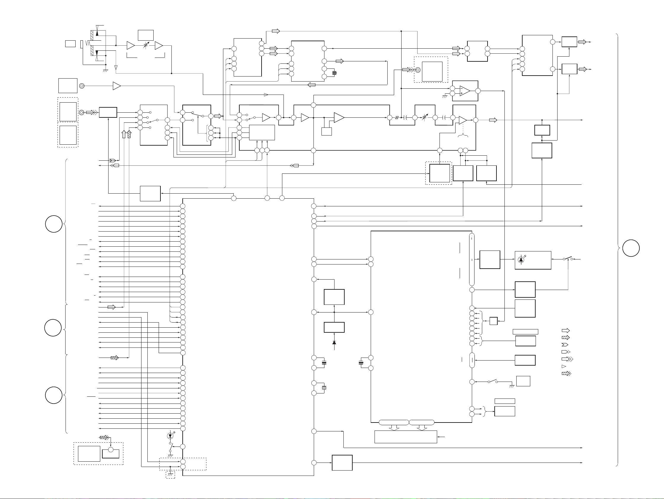
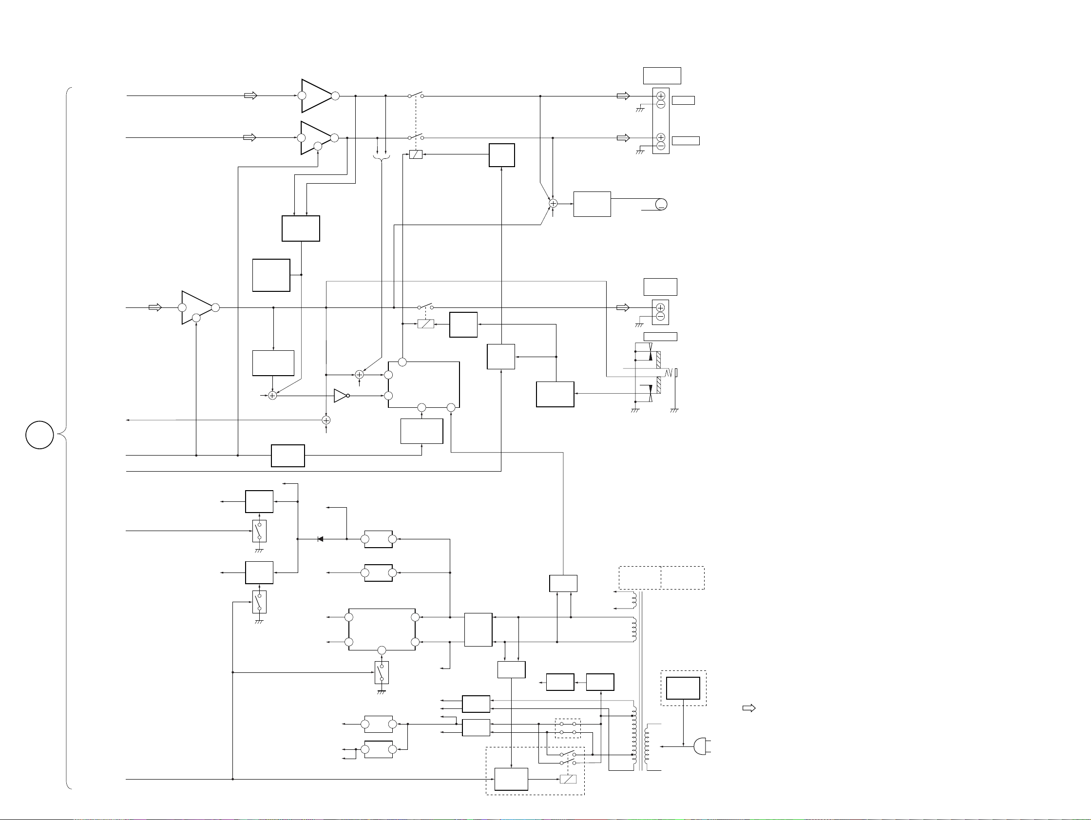
– MAIN SECTION –
J761
MIC
J101
PHONO
IN
L
XB80AV
EXCEPT
XB80AV
(Page 26)
SECTION
(Page 20,
22)
SECTION
(Page 24)
09
B
DECK
SECTION
A
TUNER
C
CD
J101
VIDEO
(AUDIO)
IN
L
J101
VIDE/MD
(AUDIO)
IN
L
REC L
RELAY REC/PB
A SHUT
B SHUT
B HALF
A HALF
A PLAY
B PLAY
PB A / B
NORM/HIGH
BIAS ON/OFF
RM ON/OFF
NR ON/OFF
REC/PB PASS
LM ON/OFF
CAP M H/L
A TRG
B TRG
TRIG H/L
CAP M ON/OFF
RDS DATA
RDS INT
COM DIN
COM DATA
STEREO
TUNED
TBL. L
TBL. R
T. SENS
SENS 2
CD CLK
CD DATA
UP SW
SQ CLK
SQ DATA
DIGITAL OUT
OPTICAL
EXCEPT XB80AV
PB L
ST L
ST CE
MUTE
L CH
SCOR
SENS
X RST
X LAT
DOUT
CD
31
PHONO EQ AMP
IC101
MUTE
Q121
1
IC841
RV760
MIC
LEVEL
31
MIC AMP
IC760
V
1
TC
2
ST
4
CD
5
67
INPUT SELECT
IC102
INH
MUTE
CONTROL
Q123,124
D201
(DISC No.)
EXCEPT
AEP,UK
A
B
D+5V
DOLBY PRO LOGIC
IC601
C-OUT
9
LIN
S-OUT
3
4
2
INPUT SELECT
IC103
3
5
3
10
9
6
96
RELAY
26
A SHUT
27
B SHUT
28
B HALF
97
A HALF
94
A PLAY SW
95
B PLAY SW
87
PB A/B
88
EQ H//N
89
BIAS
90
REC MUTE
91
NR ON/OFF
R/P PASS
92
93
TC MUTE
82
CAP H/N
83
A TRG
84
B TRG
85
TRG LOW
86
CAP M ON/OFF
1
41
VOL LAT
2
42
PL LAT
3
44
COM DOUT
4
45
COM CLK
66
ST DIN
70
STEREO
TUNED
69
68
ST CE
72
ST MUTE
67
ST DOUT
60
TBL L
61
TBL R
SCOR
18
76
T SENS
73
SENS 2
74
SENS
57
XRST
48
CD CLK
47
CD DATA
77
UP SW
36
SQ CLK
34
SQ DATA IN
58
XLT
62
TRAY LED
Q201
22
RDS DATA
21
RDS INT
4
9
10
11
INPUT CHANGE
AEP,UK
L-OUT
41
DATA
42
CLK
40
EN
69
71
28
29
30
54
MASTER CONTROL
IC701
CENTER
34
REAR
35
37
FRONT
MICON
INTERFACE
34
32 33
3
4
LATCH
3
427 LAT SW F CON
65 64
99
3
4
2
10
S-IN
8
L-IN
3
DATA
2
CLK
4
EN
DBFB H/L
TA MUTE
R RELAY
IIC DATA
CD POWER
STK MUTE
DELAY
IC602
POWER
IIC CLK
RESET
AC CUT
XT1
XT2
S-OUT
FRONT
X1
X2
L-MIX
OUT
XTAL
XTAL
61
REC 2A
62
98
2
1
7
55
56
15
20
11
10
14
13
46
100
13
16
23
24
EQ
SWITCH
D951
X701
5MHz
32.768KHz
RESET
Q951
RESET
IC951
+5V
X702
FRONT
X601
8MHz
MUTE
SWITCH
Q912
X601
8MHz
45 44 43 42
EQUALIZER / VOLUME
IC201
DATA
28
CLOCK
27
14
RESET
12
XOUT
13
XIN
SEG1-35
67 - 100 • 1
FLUORESCENT INDICATOR TUBE
J101
VIDEO/MD
(AUDIO)
OUT
L
EXCEPT XB80AV
+ +
XB80AV/XB88AV
S.WOOFER
MODE
SWITCH
Q206
DISPLAY CONTROL
IC601
GR1-16
51 - 66
FL601
39
REAR
CENTER
6
5
LED1
LED13
LED15
LED18
LED SELECT
SIRCS
SPEANA 1
SPEANA 2
SPEANA 3
SPEANA 4
JOG A
JOG B
DOOR SW
VOL A
VOL B
VF
AMP
IC861
BB22
41
40
DBFB
SWITCH
Q201
•
L+R
KEY 5
KEY 1
3
5
BB12
10
15
16
18
20
22
23
25
47
29
39
42
43
44
45
46
26
41
37
33
38
24
40
IC603
AMP
38
3
•
•
•
•
•
•
•
– 27 – – 28 –
7
1
7
FRONT
DBFB
SWITCH
Q202
LED
SWITCH
D/A
HCD-D890AV/XB55AV/XB80AV/XB88AV
VOLUME
S701
VOLUME
ROTARY
ENCODER
3
IN
14
IN
4
8
CLK
3
9
DATA
1
10
PANEL LED
LED
CONTROL
Q601
REMOTE
CONTROL
RECEIVER
IC602
S711
= AMS +
ROTARY
ENCODER
KEY
MATRIX
S681
6
OPEN
IC604
MUTE
Q254
MUTE
SWITCH
Q120
2
OUT
15
OUTLATCH
• R CH: Same as L ch
• SIGNAL PATH
: FM
: CD
: PB
: REC
: VIDEO
: MIC
: DIGITAL OUT
MUTE
Q602
MUTE
Q601
Q602,603
REAR
CENTER
FRONT
DBFB
POWER ON/OFF
R RELAY
D+5V
CD POWER
STK MUTE
REAR
CENTER
D
POWER
SECTION
(Page 29)
HCD-D890AV/XB55AV/XB80AV/XB88AV
– POWER SECTION –
REAR
REAR
1
POWER AMP
IC601
10
RY401
TM402
SURROUND
–1
REAR
SPEAKER
REAR
D
MAIN
SECTION
(Page 28)
09
CENTER
FRONT
DBFB
STK MUTE
R RELAY
CD POWER
POWER ON/OFF
FRONT
POWER AMP
IC201
1 10
6
AU/D5V SW
D5V
SW
CENTER
FAN MOTOR
DRIVER
Q961, 962
RECT
D104,105
FRONT
Rch
VF
VF
UNREG
–12V
XB80AV
T501
POWER
TRANSFORMER
M
TM401
FRONT
SPEAKER
J760
PHONES
EXCEPT XB80AV
TRANSFORMER
CENTER
M901
FAN
MOTOR
T901
POWER
E,AR
VOLTAGE
SELECTOR
S901
• R CH : Same as L ch
• SIGNAL PATH
: FM
• Abbreviation
AR: Argentine model.
AC
IN
RY402
6
PROTECTOR
PROTECT
SWITCH
VCC
2
9
VEE
POWER B+
POWER B–
–2
IC301
7
Q301
UNREG
–12V
SURR B+
SURR B–
RELAY
DRIVE
Q404
Rch
–1
RELAY
DRIVE
Q403
RELAY
CONTROL
Q402
HP / SP
SWITCHING
VFDP
Q401,405
RECT
D302,303
VF REG
Q941
EXCEPT XB80AV
RY101
4
RECT
D901
RECT
D110,111
RECT
D101
RECT
D102
RELAY
DRIVER
Q111-113
XB80AV
1318
DET
Q601,651
6
Rch
+5V
D905
D7V
A+7.5V
A–7.5V
+12V
ST10V
PRO-LOG 10V
Q323
Rch
3 1
3 1
+7.5
1
–7.5 EN
10
3 1
3 1
2
1
+5V REG
IC902
+7V REG
IC903
+7V, –7V REG
IC901
4
+12V REG
IC904
+10V REG
IC905
Q901
CENTER
Rch
CD REG
+5V REG
THERMAL
DET
Q670,671
THP670
OVER LOAD
DET
Q201
D5V
SWITCHED
Q904
Q905
Q906
Q907
OVER LOAD
MUTE
SWITCH
Q331
– 29 – – 30 –
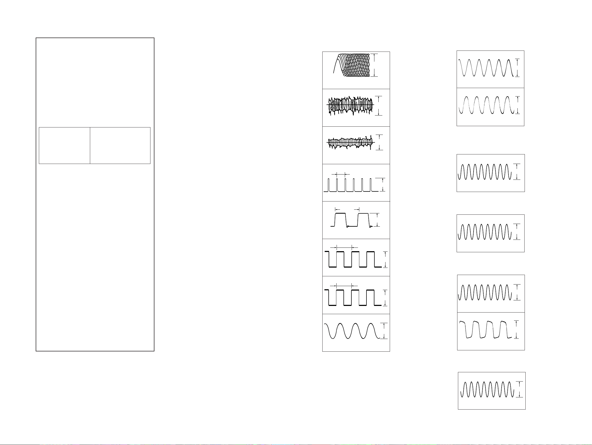
THIS NOTE IS COMMON FOR PRINTED WIRING
200mV/DIV, 1µsec/DIV
0.5Vp-p
50mV/DIV, 1msec/DIV
0.2Vp-p
230µsec
5Vp-p
135µsec
5Vp-p
135µsec
5Vp-p
BOARDS AND SCHEMATIC DIAGRAMS.
(In addition to this, the necessary note is printed
in each block.)
For schematic diagrams.
Note:
• All capacitors are in µF unless otherwise noted. pF: µµF
50 WV or less are not indicated except for electrolytics
and tantalums.
• All resistors are in Ω and
specified.
¢
•
: internal component.
• 2 : nonflammable resistor.
• 5 : fusible resistor.
• C : panel designation.
Note:
The components identified by mark ! or dotted
line with mark ! are critical for safety.
Replace only with part
number specified.
1
/4 W or less unless otherwise
Note:
Les composants identifiés par
une marque ! sont critiques
pour la sécurité.
Ne les remplacer que par une
piéce portant le numéro
spécifié.
WAVEFORMS
– CD SECTION –
1
500mV/DIV, 500nsec/DIV
IC101 #£ RFO
2
IC101 2 FEI
3
IC101 $¶ TEI
1.3Vp-p
– TUNER SECTION –
(AEP, UK, German model)
1
4.2Vp-p
4.5MHz
IC21 @¢ XOUT
2
2Vp-p
4.332MHz
IC1752 !¢
– TUNER SECTION –
(East European, CIS model)
1
• U : B+ Line.
• V : B– Line.
• H : adjustment for repair.
• Voltages and waveforms are dc with respect to ground
under no-signal (detuned) conditions.
• V oltages are taken with a V OM (Input impedance 10 MΩ).
Voltage variations may be noted due to normal production tolerances.
• Waveforms are taken with a oscilloscope.
Voltage variations may be noted due to normal production tolerances.
• Circled numbers refer to waveforms.
• Signal path.
F : FM
f : AM
E : PB (DECK A)
d : PB (DECK B)
G : REC (DECK B)
J : CD
c : digital out
I : PHONO
• Abbreviation
CND : Canadian model.
EE : East European model.
AUS : Australian model.
AR : Argentine model.
MX : Mexican model.
For printed wiring boards.
Note:
• X : parts extracted from the component side.
•
p : parts mounted on the conductor side.
®
•
•
• b : Pattern from the side which enables seeing.
(The other layers' patterns are not indicated.)
: Through hole.
¢
: internal component.
4
5
6
7
8
7.8µsec
IC103 @¶ MDP
IC103 ^º XPCK
IC103 ^™ RFCK
IC103 &¢ WFCK
16.9344MHz
IC103 *ª XTAI
2.5Vp-p
2.6Vp-p
4.2Vp-p
4.5MHz
IC21 @¢ XOUT
– MAIN SECTION (1/5) –
1
4.8Vp-p
8MHz
IC602 @¢ XTAL
– MAIN SECTION (2/5) –
1
5.5Vp-p
8MHz
IC701 0 X2
2
5.2Vp-p
32.768kHz
IC701 !£ XT2
– 31 –
– DISPLAY SECTION –
1
4Vp-p
8MHz
IC601 !™ X-OUT
– 32 –
HCD-D890AV/XB55AV/XB80AV/XB88AV
d
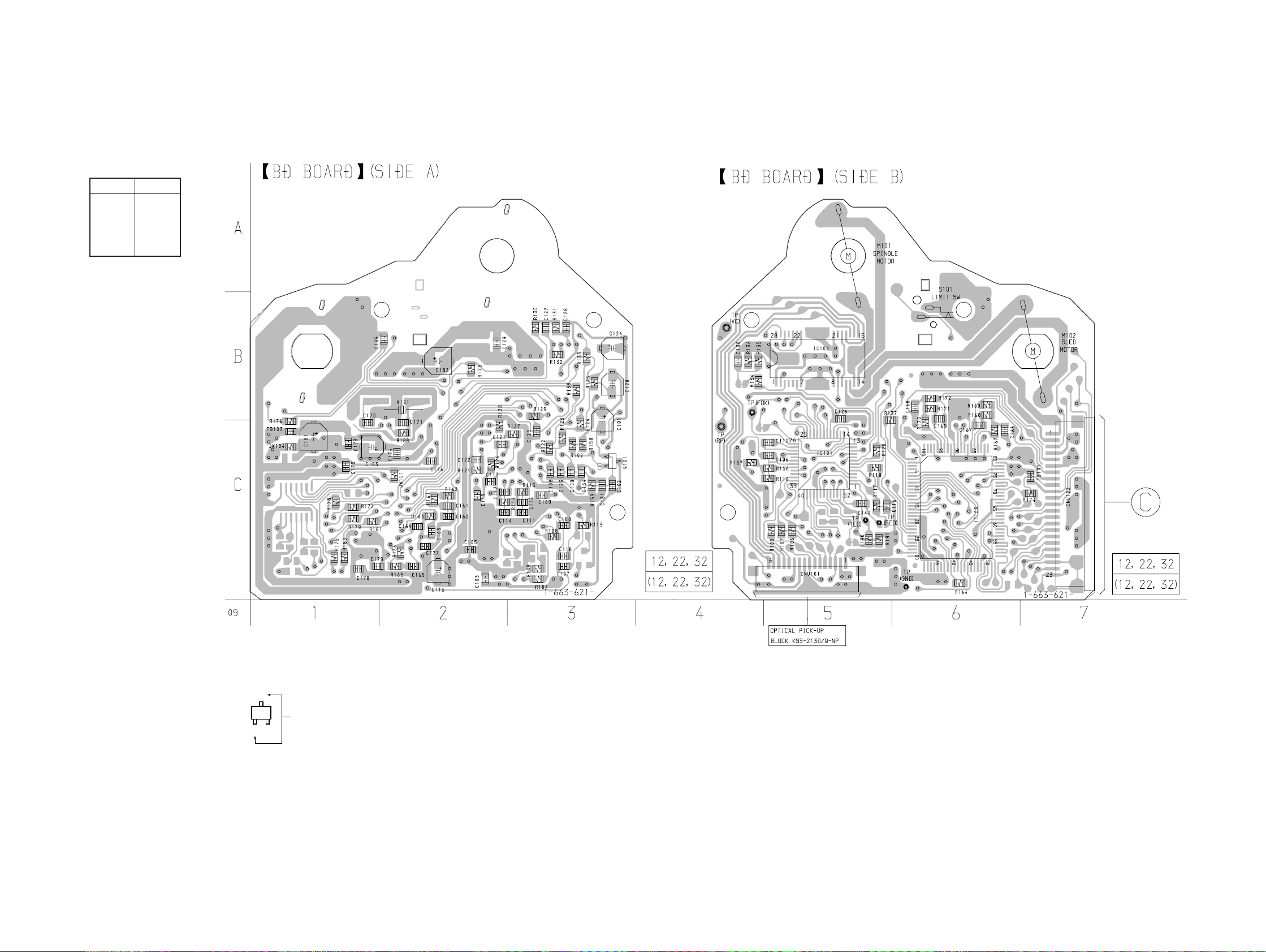
6-3. PRINTED WIRING BOARD – CD SECTION –
• See page 18 for Circuit Boards Location.
• Semiconductor
Location
Ref. No. Location
IC101 C-5
IC102 B-5
IC103 C-6
Q101 C-3
• Indication of transistor
C
Q
These are omitte
EB
(Page 44)
– 33 – – 34 –

6-4. SCHEMATIC DIAGRAM – CD SECTION –
• See page 32 for Waveforms.
• See page 87 for IC Block Diagrams.
• See page 92 for IC Pin Functions.
HCD-D890AV/XB55AV/XB80AV/XB88AV
(Page 48)
– 35 – – 36 –
HCD-D890AV/XB55AV/XB80AV/XB88AV
6-5. SCHEMATIC DIAGRAM – TUNER SECTION – (AEP, UK model)
• See page 32 for Waveforms.
• See page 85 for IC Block Diagrams.
(Page 45)
– 37 – – 38 –

HCD-D890AV/XB55AV/XB80AV/XB88AV
d
6-6. PRINTED WIRING BOARD – TUNER SECTION – (AEP, UK model)
• See page 18 for Circuit Boards Location.
• Semiconductor
Location
Ref. No. Location
D21 D-1
D41 D-2
D42 E-3
D1751 F-2
IC21 D-1
IC41 C-3
IC1751 E-1
IC1752 F-3
Q1 D-1
Q2 D-1
Q3 C-2
Q4 C-2
Q5 C-2
Q9 B-1
Q11 B-3
Q12 A-3
Q13 A-2
Q14 A-2
(Page 44)
• Indication of transistor
C
Q
These are omitte
EB
– 39 –

HCD-D890AV/XB55AV/XB80AV/XB88AV
d
6-7. PRINTED WIRING BOARD – TUNER SECTION – (East European, CIS model)
• See page 18 for Circuit Boards Location.
• Semiconductor
Location
Ref. No. Location
D1 D-1
D41 D-2
D42 E-3
D43 E-3
D1701 F-2
D1702 F-2
D1703 E-2
D1704 F-2
IC21 D-1
IC41 C-3
IC1701 F-1
IC1702 F-3
Q1 D-1
Q2 D-2
Q3 C-2
Q4 C-2
Q5 C-2
Q9 B-1
Q11 B-3
Q12 A-3
Q13 A-2
Q14 A-2
Q1701 E-2
Q1702 F-2
Q1703 F-2
• Indication of transistor
C
Q
These are omitte
EB
(Page 44)
– 40 –
 Loading...