

Sony HCD-VX550 Service manual

HCD-VX550
SERVICE MANUAL
HCD-VX550 is the Amplifier, Video
CD player, Tape Deck and Tuner
section in MHC-VX550.
Dolby noise reduction manufactured under license
from Dolby Laboratories Licensing Corporation.
“DOLBY” and the double-D symbol a are trademarks of Dolby Laboratories Licensing Corporation.
CD
Section
Tape deck
Section
Chinese Model
Model Name Using Similar Mechanism NEW
CD Mechanism Type CDM38LH-5BD36L
Base Unit Name BU-26BD36L
Optical Pick-up Name KSS-213D/Q-RP
Model Name Using Similar Mechanism HTC-V5550
Tape Transport Mechanism Type TCM-230AWR2
Amplifier section
The following measured at AC 120, 220, 240 V 50/60
Hz
DIN power output (rated)110 + 110 W
(8 Ω at 1 kHz, DIN)
Continuous RMS power output (reference)
140 + 140 W
(8 Ω at 1 kHz, 10% THD)
Inputs
MD IN: voltage 450 mV,
(phono jacks) impedance 47 kΩ
VIDEO (AUDIO) IN: voltage 250 mV,
(phono jacks) impedance 47 kΩ
MIC 1/2 (phone jack): sensitivity 1 mV, impedance
10 kΩ
SPECIFICATIONS
Outputs
MD OUT (phono jacks): voltage 250 mV
impedance 1 kΩ
VIDEO OUT (phono jack):
max,output level
1Vp-p, unbalanced, Sync
negative, load impedance
75 Ω
S-VIDEO OUT (4-pin/ mini-DIN jack):
Y: 1Vp-p, unbalanced,
Sync negative,
C: 0.286Vp-p,
load impedance 75 Ω
PHONES (stereo phone jack):
accepts headphones of 8 Ω
or more
SPEAKER: accepts impedance of 8 to
16 Ω
SUPER WOOFER Voltage 1 V, impedance
kΩ
MINI Hi-Fi COMPONENT SYSTEM
SUPER VIDEO CD/VIDEO CD
/CD player section
System Compact disc and digital
Laser Semiconductor laser
Laser output Max. 44.6 µW*
Frequency response 2 Hz - 20 kHz (±0.5 dB)
Wavelength 780 -790 nm
Signal-to-noise ratio More than 90 dB
Dynamic range More than 90 dB
1
Video color system format
audio and video system
(λ=780nm)
Emission duration:
continuous
*This output is the value
measured at distance of 200
mm from the objective lens
surface on the Optical Pick-up
Block with 7 mm aperture.
NTSC, PAL
Continued on next page
MICROFILM

CD OPTICAL DIGITAL OUT
(Square optical connector jack, rear panel)
Wavelength 660 nm
Output Level –18 dBm
TABLE OF CONTENTS
1. SERVICING NOTES·················································3
Tape player section
Recording system 4-track 2-channel stereo
Frequency response 40 - 13,000 Hz (±3 dB),
(DOLBY NR OFF) using Sony TYPE I cassette
40-14,000 Hz (± 3 dB),
using Sony TYPE II cassette
Tuner section
Fm stereo, FM/ AM superheterodyne tuner
FM tuner section
Tuning range 87.5-108.0 MHz
Antenna FM lead antenna
Antenna terminals 75 Ω unbalanced
Intermediate frequency 10.7 MHz
AM tuner section
Tuning range
2 Band type: 531-1,602 kHz
(with the interval set at 9 kHz)
530-1,710 kHz
(with the interval set at 10 kHz)
3 Band type:
MW: 531-1,602 kHz
(with the interval set at 9 kHz)
530-1,710 kHz
(with the interval set at 10 kHz)
SW: 5.95-17.90 MHz
(with the interval set at 5 kHz)
Antenna AM loop antenna
Antenna terminals External antenna terminal
Intermediate frequency 450 kHz
General
Power requirements 220 V AC, 50/ 60 Hz
Power consumption: 160 W
Dimensions (w/h/d) Approx. 280 × 340 × 395 mm
Mass: Approx. 10.0 kg
Design and specifications are subject to change without notice.
2. GENERAL .......................................................................... 5
3. DISASSEMBLY ................................................................ 8
4. TEST MODE................................................................... 11
5. MECHANICAL ADJUSTMENTS ............................ 14
6. ELECTRICAL ADJUSTMENTS
DECK Section .................................................................. 14
CD Section ....................................................................... 17
VIDEO Section.................................................................17
7. DIAGRAMS
7-1. Block Diagram
CD SERVO Section.......................................................... 18
AUDIO/VIDEO CD Section ............................................ 19
TAPE DECK Section ....................................................... 20
MAIN Section .................................................................. 21
DISPLAY/KEY CONTROL/
POWER SUPPLY Section················································22
7-2. Circuit Board Location ····················································· 23
7-3. Printed Wiring Board BD Board .................................... 24
7-4. Schematic Diagram BD Board ....................................... 25
7-5. Schematic Diagram VIDEO Board (1/2)........................26
7-6. Schematic Diagram VIDEO Board (2/2)........................27
7-7. Printed Wiring Board VIDEO Board..............................28
7-8. Printed Wiring Boards CD MOTOR Section ................. 30
7-9. Schematic Diagram CD MOTOR Section......................31
7-10. Printed Wiring Board AUDIO Board ............................. 32
7-11. Schematic Diagram AUDIO Board ................................ 33
7-12. Printed Wiring Board LEAF SW Board.........................34
7-13. Schematic Diagram LEAF SW Board............................34
7-14. Printed Wiring Board MAIN Board ............................... 35
7-15. Schematic Diagram MAIN Board (1/4) ......................... 36
7-16. Schematic Diagram MAIN Board (2/4) ......................... 37
7-17. Schematic Diagram MAIN Board (3/4) ......................... 38
7-18. Schematic Diagram MAIN Board (4/4) ......................... 39
7-19. Printed Wiring Board PANEL Board ............................. 40
7-20. Schematic Diagram PANEL Board ................................ 41
7-21. Printed Wiring Board CD SW/5V POWER Board ........ 42
7-22. Schematic Diagram CD SW/5V POWER Board ........... 42
7-23. Printed Wiring Board TRANSFORMER Board ............ 43
7-24. Schematic Diagram TRANSFORMER Board ............... 43
7-25. Printed Wiring Board SURROUND Board .................... 44
7-26. Schematic Diagram SURROUND Board....................... 44
7-27. IC Block Diagrams ........................................................... 45
7-28. IC Pin Function Description............................................. 49
8. EXPLODED VIEWS ..................................................... 60
9. ELECTRICAL PARTS LIST..................................... 68
2
SECTION 1
3
SERVICING NOTES
SELF-DIAGNOSIS
This unit is equipped with a self-diagnosis function.
The function is used for diagnosing the conditions of the circuits of
the VIDEO board.
The circuits can be determined if normal or abnormal by the lighting
of D502 of the VIDEO board.
Lighting of D502
When lit : Operates normally
Blinks repeatedly : The circuit may be faulty.
VIDEO Board (SIDE B)
CN501
100
31
30
1
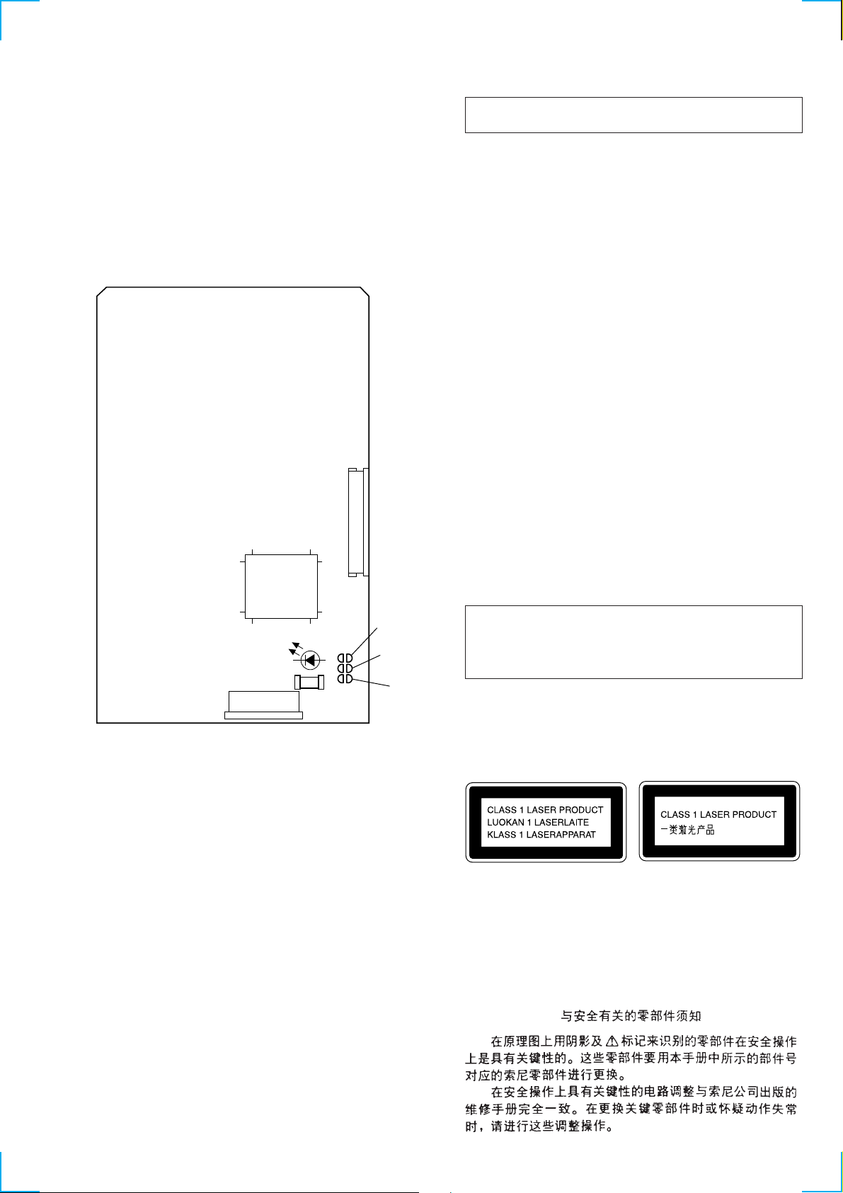
NOTES ON HANDLING THE OPTICAL PICK-UP
BLOCK OR BASE UNIT
The laser diode in the optical pick-up block may suffer electrostatic
break-down because of the potential difference generated by the
charged electrostatic load, etc. on clothing and the human body.
During repair, pay attention to electrostatic break-down and also
use the procedure in the printed matter which is included in the
repair parts.
The flexible board is easily damaged and should be handled with
care.
NOTES ON LASER DIODE EMISSION CHECK
The laser beam on this model is concentrated so as to be focused on
the disc reflective surface by the objective lens in the optical pickup block. Therefore, when checking the laser diode emission,
observe from more than 30 cm away from the objective lens.
Notes on chip component replacement
• Never reuse a disconnected chip component.
• Notice that the minus side of a tantalum capacitor may be damaged by heat.
Flexible Circuit Board Repairing
• Keep the temperature of the soldering iron around 270 ˚C during repairing.
• Do not touch the soldering iron on the same conductor of the
circuit board (within 3 times).
• Be careful not to apply force on the conductor when soldering
or unsoldering.
IC505
50
51 80
CN502
D502
81
SL501
SL502
SL50
CAUTION
Use of controls or adjustments or performance of procedures
other than those specified herein may result in hazardous
radiation exposure.
This appliance is classified as a CLASS 1 LASER product.
The CLASS 1 LASER PRODUCT MARKING is located on
the rear exterior.
Laser component in this product is capable of emitting radiation
exceeding the limit for Class 1.
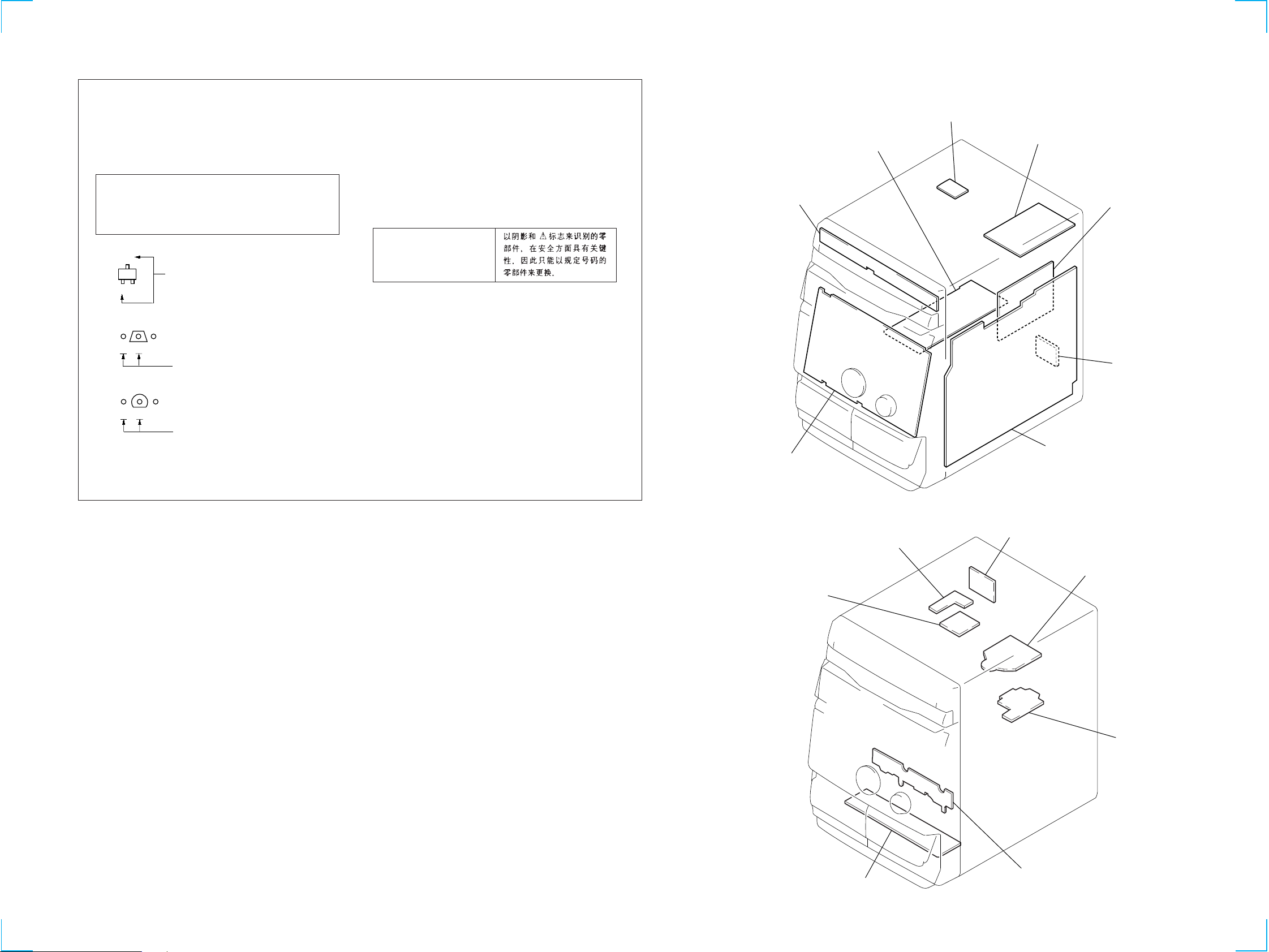
SAFETY-RELATED COMPONENT WARNING!!
COMPONENTS IDENTIFIED BY MARK ! OR DOTTED LINE WITH
MARK ! ON THE SCHEMATIC DIAGRAMS AND IN THE PARTS
LIST ARE CRITICAL TO SAFE OPERATION. REPLACE THESE
COMPONENTS WITH SONY PARTS WHOSE PART NUMBERS
APPEAR AS SHOWN IN THIS MANUAL OR IN SUPPLEMENTS
PUBLISHED BY SONY .
3
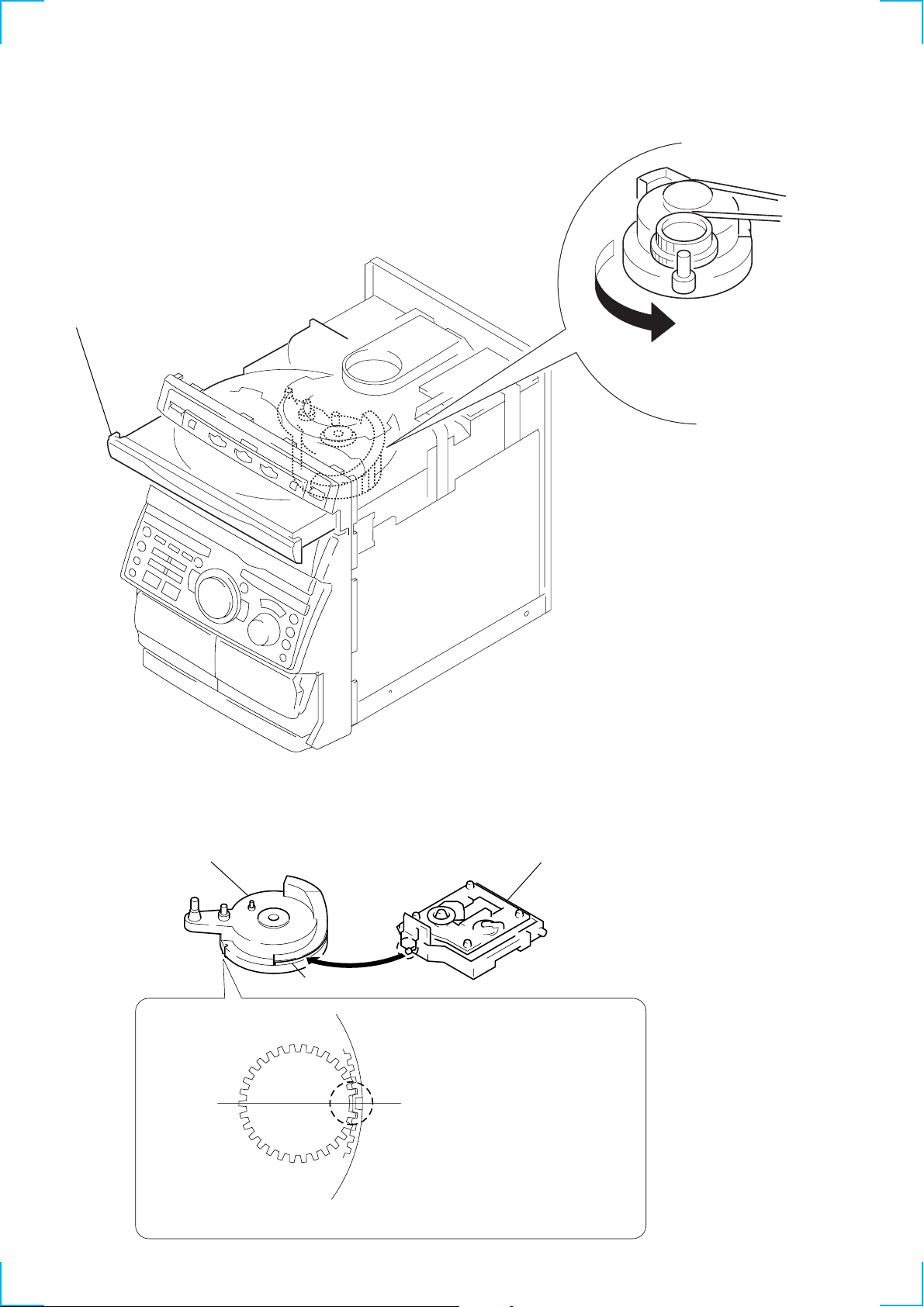
HOW TO OPEN THE DISC TRAY WHEN POWER SWITCH TURNS’ OFF.
e
1
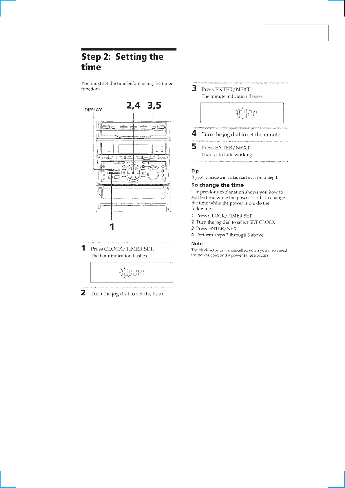
Remove the Case.
3
Pull-out the disc tray.
2
Turn the cam to the
direction of arrow.
NOTE FOR INSTALLATION (ROTARY ENCODER)
BU cam
Groove
Note:When attaching the Base unit, Insert th
section A into the groove of BU cam.
Section A
Note:When attaching the BU cam,
engage the Rotary encoder
switch as shown in the figure.
4
• LOCATION OF CONTENTS
Front View
SECTION 2
GENERAL
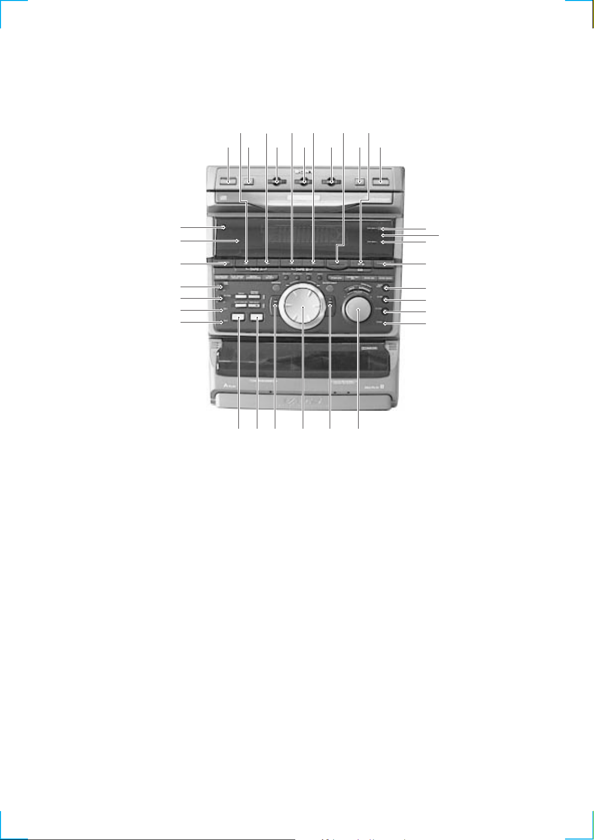
qs08642
13 5 7 9 qa
qd
ef
ed
es
ea
e;
wl
wk
1 1/u button
2 9 TAPE A button and indicator
3 (STANDBY) DEMO button
4 ( TAPE A button and indicator
5 DISC 1 button
6 9 TAPE B button and indicator
7 DISC 2 button
8 ( TAPE B button and indicator
9 DISC 3 button
0 p button
qa DISC SKIP, EX-CHANGE button
qs ^ CD button and indicator
qd § button
qf SVCD/VCD indicator
qg PBC indicator
qh PBC OFF indicator
qj TUNER/BAND button
qf
qg
qh
qj
qk
ql
w;
wa
wswdwfwgwhwj
qk REC PAUSE/START button and indicator
ql HI-DUB button
w; CD SYNC button
wa PHONE jack
ws VOLUME knob
wd + ) button and indicator
wf JOG dial and indicator
wg – 0 button and indicator
wh CD FLASH button
wj CD LOOP button
wk MIC 2 jack
wl MIC 1 jack
e; MIC LEVEL knob
ea ECHO LEVEL knob
es FUNCTION button
ed SYNC EQ indicator
ef EFFECT indicator
5
eg eh ej ek el r; ra rs rd rf
rg
rh
rj
rk
rlt;tatstdtftgth
eg EDIT/DIRECTION
TUNER MEMORY button
eh PLAY MODE, DOLBY NR button
ej REPEAT STEREO/MONO button
ek FILE SELECT button
el SELECT button
r; RETURN button
ra PREV button
rs NEXT button
rd CD NON-STOP button and indicator
rf KARAOKE PON/MPX button
rg SYNC BASS H indicator
rh SYNC BASS L indicator
rj SYNC EQ button
rk SYNC BASS button
rl CINEMA SPACE/SURROUND button
t; DBFB button
ta ENTER/NEXT button and indicator
ts GROOVE button and indicator
td SPECTRUM ANALYZER button
tf TIMER SELECT button and indicator
tg CLOCK/TIMER SET button
th DISPLAY button
6
This section is extracted
from instruction manual.
7
SECTION 3
DISASSEMBLY
Note : Follow the disassembly procedure in the numerical order given.
3-1. COVER
6
cover
2
screw
3
two screws
(case 3TP2) (3
(case 3TP2) (3
×
8)
×
12)
5
4
4
1
three screws
(BVTP3
2
screw
(case 3TP2) (3
3
two screws
(case 3TP2) (3
×
8)
×
12)
×
8)
3-2. LOADING PANEL ASS’Y
A
1
Turn the cam-in the
direction of the arrow
A
2
Pull-out
the disc tray.
3
loading panel ass’y
.
8
3-3. FRONT PANEL SECTION
)
4
screw
(BVTT3
×
10)
6
front panel section
1
wire (flat type)
(15 core) (32 cm) (CN303)
2
screw
(BVTT3
×
6)
3
two lugs
4
screw
(BVTP3
×
10)
3
lug
2
1
wire (flat type)
(23 core) (23 cm) (CN501)
screw
(BVTT3
×
6
1
wire (flat type) (17 core)
5
two screws
(BVTT3
×
6)
(CN304)
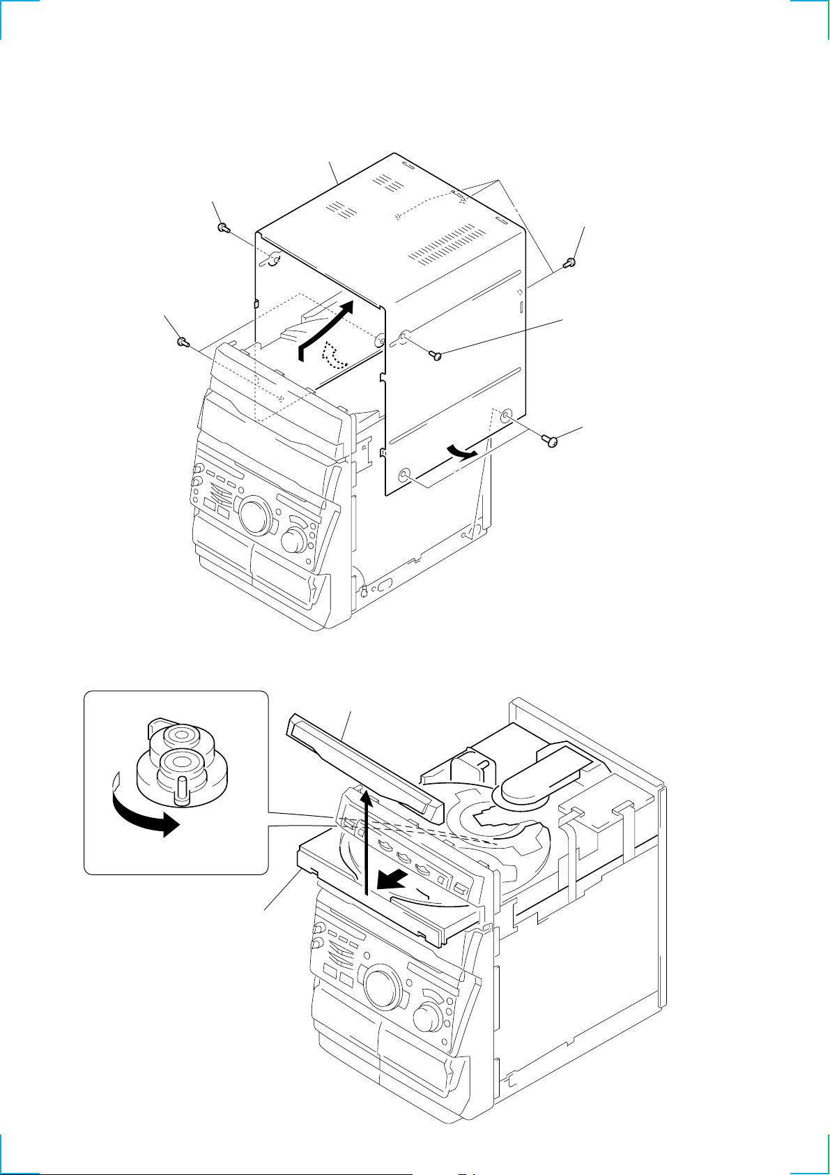
3-4. VIDEO BOARD, CD MECHANISM DECK SECTION (CDM38LH-5BD36L)
8
Remove the CD mechanism
deck (CDM38LH-5BD36L)
in the direction of arrows
A
– B.
6
screw
(BVTP3
×
10)
B
A
wire (flat type)
1
(15 core) (17 cm) (CN502)
2
two screws
×
(BVTP3
8)
7
two screws
(BVTP3
×
5
8)
2
screw
(BVTP3
chassis
×
8)
3
VIDEO
board
1
wire (flat type)
(25 core) (18 cm)
(CN501)
4
screw
(BVTP3
×
8)
6
screw
(BVTP3
9
two connectors
(CN392, 393)
×
10)
9
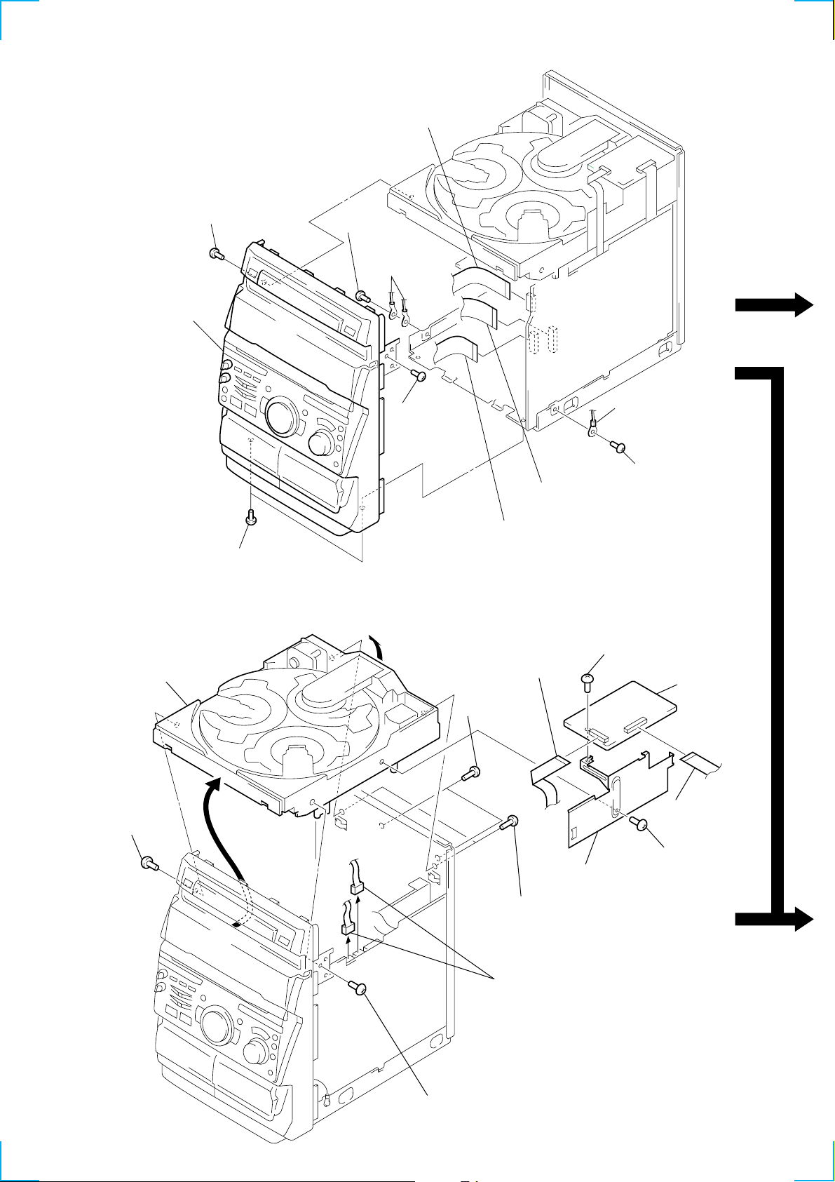
3-5. TAPE MECHANISM DECK SECTION (TCM-230AWR2)
)
2
Open two
cassette lids.
1
Push the cassette lid.
3
three screws
(BVTP2.6
×
8)
3
two screws
(BVTP2.6
4
tape mechanism deck section
(TCM-230AWR2)
×
8)
3-6. MAIN BOARD
2
connector
(CN952)
1
Push the cassette lid.
2
connector
(CN953)
3
two screws
(BVTP3 × 8)
1
wire (flat type)
(15 core)(15 cm)(CN371)
5
five screws
(BVTP3 × 8
10
6
Remove the MAIN board
in the direction of the arrow.
4
two screws
(BVTP3 × 8)
7
connector
(CN403)

SECTION 4
TEST MODE
[MC Cold Reset]
• The cold reset clears all data including preset data stored in the
RAM to initial conditions. Execute this mode when returning
the set to the customer.
Procedure:
1. Turn the power ON or set to the DEMO mode.
2. Press three buttons of p , ENTER/NEXT , and 1 /u
simultaneously.
3. The set is reset, and displays “COLD RESET”, then becomes
DEMO mode.
[MC Hot Reset]
• This mode resets the set with the preset data kept stored in the
memory. The hot reset mode functions same as if the power
cord is plugged in and out.
Procedure:
1. Turn the power ON or set to the DEMO mode.
2. Press three buttons of p , ENTER/NEXT , and DISC1
simultaneously.
3. The set is reset, and becomes standby state.
[Change-over the AM Tuning Interval]
(EXCEPT Saudi Arabia model)
• The AM tuning interval can be changed over 9 kHz or 10 kHz.
Procedure:
1. Press the 1/u button to turn the power ON.
2. Select the function “TUNER”, and press the TUNER/BAND
button to select the BAND “AM (MW)”.
3. Press the 1/u button to turn the power OFF.
4. Press the ENTER/NEXT and 1/u buttons simultaneously, and
the display on the fluorescent indicator tube changes to “ AM 9
k STEP” or “AM 10 k STEP”, and thus the tuning interval is
changed over.
[CD Delivery Mode]
• This mode moves the optical pick-up to the position durable to
vibration. Use this mode when returning the set to the customer
after repair.
Procedure:
1. Press the 1/u button to turn the power ON.
2. Press the CD LOOP and 1/u buttons simultaneously.
3. A message “LOCK” is displayed on the fluorescent indicator
tube, and the CD delivery mode is set.
[LED and Fluorescent Indicator Tube All Lit, Key Check
Mode]
Procedure:
1. Press three buttons of p , ENTER/NEXT , and DISC1
simultaneously.
2. LEDs and fluorescent indicator tube are all turned on.
Press the DISC1 button, and the key check mode is activated.
3. In the key check mode, the fluorescent indicator tube displays
“K 0 J0 V0”. Each time a button is pressed, “K” value increases.
However, once a button is pressed, it is no longer taken into
account.
“J” value increases like 1, 2, 3 ... if turn the JOG dial clockwise,
or it decreases like 0, 9, 8 ... if turn the JOG dial
counterclockwise.
“V” value increases like 1, 2, 3 ... if turn the VOLUME dial
clockwise, or it decreases like 0, 9, 8 ... if turn the JOG dial
counterclockwise.
4. To exit from this mode, press three buttons in the same manner
as step 1, or disconnect the power cord.
11

[Aging Mode]
This mode can be used for operation check of tape deck section.
Tape deck section work in parallel.
• If an error occurred:
The aging operation stops and display then status.
• If no error occurs:
The aging operation continues repeatedly.
Procedure:
1. Load the tapes into the decks A and B respectively.
2. Press the FUNCTION button to select the function “CD”.
3. Press the PLAY MODE button to set the “ ALL DISCS” mode,
and press the REPEAT button to “REPEAT” off.
4. Press three buttons of p , ENTER/NEXT , and DISC SKIP/
EX-CHANGE simultaneously.
5. The aging mode is activated, if the indicator of disc tray number
on the fluorescent indicator tube is blinking.
6. To exit from the aging mode, press the 1/u button to turn the
power OFF and operate the cold reset. (Refer to the “MC Cold
Reset”)
1. Display at the Aging Mode
• Display operating state of tape deck section alternately.
• If an error occurred, stop display.
2. Tape Deck Section
• The sequence during the aging mode is following as below.
• If an error occurred, stop display that step.
Aging mode sequence (Tape deck section) :
Rewind the tape A and B
“TAPE A AG-1”
Shut off
FWD play the tape A
“TAPE A AG-2”
2 minutes
Fast forward the tape A
“TAPE A AG-3”
Shut off or 20 seconds
REV play the tape A
“TAPE A AG-4”
2 minutes
Rewind the tape A
“TAPE A AG-5”
Shut off
FWD play the tape B
“TAPE B AG-2”
2 minutes
Fast forward the tape B
“TAPE B AG-3”
Shut off or 20 seconds
REV play the tape B
“TAPE A AG-4”
2 minutes
Rewind the tape B
“TAPE B AG-5”
Shut off
Note: “TAPE * AG-*” is display of each step.
12
[VIDEO CD Color-bars Mode]
On this mode, the data of the color-bars signal as a picture signal
and the 1 kHz sine wave signal as a sound signal are output by the
mechanism controller (IC505) for the video CD signal check. When
measurement of the voltage and waveform on the VIDEO board,
perform it in this mode.
For reference, the color-bars signal can be observed at J502 (VIDEO
OUT) and the sound signal can be observed at J101 (VIDEO/MD
(AUDIO) OUT) using an oscilloscope.
Procedure:
1. Short the both ends of the land of SL503 of the VIDEO board.
2. Turn the power on. Press the FUNCTION button to select CD.
3. The color-bars appears when the CD is in stop status, and it
disappears when the CD goes in play status.
4. After measuring, remove the lead wire connected.
VIDEO board (SIDE B)
3150
30
1
10081
CN501
CN502
SL503
51
IC505
80
SL501
SL502
13
SECTION 5
r
MECHANICAL ADJUSTMENTS
SECTION 6
ELECTRICAL ADJUSTMENTS
Precaution
1. Clean the following parts with a denatured alcohol-moistened
swab:
record/playback heads pinch rollers
erase head rubber belts
capstan idlers
2. Demagnetize the record/playback head with a head
demagnetizer.
3. Do not use a magnetized screwdriver for the adjustments.
4. After the adjustments, apply suitable locking compound to the
parts adjusted.
5. The adjustments should be performed with the rated power
supply voltage unless otherwise noted.
Torque Measurement
Mode
FWD
FWD
back tension
REV
REV
back tension
FF/REW
FWD tension
REV tension
Torque meter
CQ-102C
CQ-102C
CQ-102RC
CQ-102RC
CQ-201B
CQ-403A
CQ-403R
Meter reading
31 to 71 g • cm
(0.43 - 0.98 oz • inch)
2 to 6 g • cm
(0.03 - 0.08 oz • inch)
31 to 71 g • cm
(0.43 - 0.98 oz • inch)
2 to 6 g • cm
(0.03 - 0.08 oz • inch)
71 to 143 g • cm
(0.99 - 1.99 oz • inch)
100 g or more
(3.53 oz or more)
100 g or more
(3.53 oz or more)
DECK SECTION
1. Demagnetize the record/playback head with a head
demagnetizer.
2. Do not use a magnetized screwdriver for the adjustments.
3. After the adjustments, apply suitable locking compound to the
parts adjust.
4. The adjustments should be performed with the rated power
supply voltage unless otherwise noted.
5. The adjustments should be performed in the order given in this
service manual. (As a general rule, playback circuit adjustment
should be completed before performing recording circuit
adjustment.)
6. The adjustments should be performed for both L-CH and RCH.
7. Switches and controls should be set as follows unless otherwise
specified.
8. Set to the DOLBY NR OFF.
9. Set to the test mode.
(1) Press the 1/u button to turn the power ON.
(2) Select the function “TAPE A or B”.
(3) Press the button of p , ENTER/NEXT , and DISC3
simultaneously, to set the tape deck test mode and blink
the indicator of disc tray number on the fluorescent indicator
tube.
(4) To exit from the test mode, press the 1/u button.
• Test T ape
Tape Signal Used for
P-4-A100 10 kHz, -10 dB Azimuth Adjustment
WS-48B 3 kHz, 0 dB Tape Speed Adjustment
P-4-L300 315 Hz, 0 dB Level Adjustment
0 dB = 0.775 V
Record/Playback Head Azimuth Adjustment
DECK A DECK B
Note: Perform this adjustments for both decks
Procedure:
1. Mode: Playback (FWD)
test tape
P-4-A100
(10 kHz, – 10 dB)
MAIN board
MD OUT jack (J101)
L-CH, R-CH
level mete
set
+
–
14
2. Turn the adjustment screw and check output peaks. If the peaks
+
–
set
test tape
WS-48B
(3 kHz, 0 dB)
MAIN board
MD OUT jack (J101)
L-CH, R-CH
frequency counter
r
do not match for L-CH and R-CH, turn the adjustment screw so
that outputs match within 1dB of peak.
Tape Speed Adjustment DECK B
Mode: Playback
Output
level
within
1dB
L-CH
peak
R-CH
peak
within
1dB
Screw
position
L-CH
peak
Screw
position
R-CH
peak
3. Mode: Playback
MAIN board
test tape
P-4-A100
(10 kHz, – 10 dB)
L-CH
set
R-CH
in phase 45°90°135°180
MD OUT jack (J101)
L-CH
R-CH
waveform of oscilloscope
good
oscilloscope
wrong
H
V
°
4. Repeat step 1 to 3 in playback (REV) mode.
5. After the adjustments, apply suitable locking compound to the
pats adjusted.
1. Insert the WS-48B into the deck B.
2. Press the ( button on the deck B.
3. Press the HI-DUB button in playback mode.
Then at HIGH speed mode.
4. Adjust RV1001 on the LEAF SW board do that frequency
counter reads 6,000 ± 180 Hz.
5. Press the HI-DUB button.
Then back to NORMAL speed mode.
6. Adjust RV1002 on the LEAF SW board so that frequency
counter reads 3,000 ± 90 Hz.
Adjustment Location: LEAF SW board
Sample value of Wow and Flutter: 0.3% or less W.RMS (JIS)
(WS-48B)
Playback level Adjustment DECK A DECK B
Procedure:
Mode: Playback
test tape
P-4-L300
(315 Hz, 0 dB)
set
MAIN board
MD OUT jack (J101)
L-CH, R-CH
level mete
+
–
Adjustment Location: Playback Head (Deck A).
Record/Playback/Erase Head (Deck B).
forward
reverse
Deck A is RV311 (L-CH) and RV411 (R-CH), Deck B is RV301
(L-CH) and R V401 (R-CH) so that adjustment within specification
values as follows.
Specification V alues:
J101 PB level: 301.5 to 338.3 mV (-8.2 to -7.2 dB) level
difference between the channels: within ± 0.5 dB
Adjustment Location: AUDIO board
15

REC Bias Adjustment DECK B
r
r
Procedure:
1. Mode: Record
FUNCTION: VIDEO
MAIN board
VIDEO (AUDIO) IN jack (J101)
L-CH, R-CH
50 mV (– 23.8 dB)
600
Ω
AF OSC
1) 315 Hz
2) 10 kHz
attenuator
2. Mode: Playback
set
blank tape
CN-123
Specification values:
J101 PB level: 47.2 to 53.0 mV (- 24.3 to - 23.3 dB)
Adjustment Location: MAIN board
MAIN BOARD (Conductor Side)
RV301
L
IC301
RV351
R
REC LEVEL
VIDEO (AUDIO) IN
J101
MD OUT
(L/R)
(L/R)
recorded
portion
set
MAIN board
MD OUT jack (J101)
L-CH, R-CH
level mete
+
–
3. Confirm playback the signal recorded in step 1 become
specification values as follows.
If these values are out of specification values, adjust the RV341
(L-CH) and RV441 (R-CH) on the A UDIO board to repeat steps
1and 2.
Specification values: Playback output of 315 Hz to playback
output of 10 kHz: ± 0.5 dB
Adjustment Location: AUDIO board
REC Level Adjustment DECK B
Procedure:
1. Mode: Record
FUNCTION: VIDEO
MAIN board
VIDEO (AUDIO) IN jack (J101)
L-CH, R-CH
AF OSC
315 Hz, 50 mV (– 23.8 dB)
Ω
attenuator
600
blank tape
CS-123
set
AUDIO BOARD (Component Side)
RV441
RV401
RV301
LR
PB LEVEL
– DECK B –
IC602
RV341
RL
REC BIAS
CN601
RV311
LEAF SW BOARD (Component Side)
TAPE SPEED
(NORMAL) (HIGH)
RV1002
RV1001
CN1001
RV411
LR
PB LEVEL
– DECK A –
2. Mode: Playback
recorded
portion
set
MAIN board
MD OUT jack (J101)
L-CH, R-CH
level mete
+
–
3. Confirm playback the signal recorded in step 1 become
specification values as follows.
If these values are out of specification values, adjust the RV301
(L-CH) and R V351 (R-CH) on the MAIN board to repeat steps
1 and 2.
16

CD SECTION
V
)
+
–
(27 MHz)
VIDEO board
frequency counter
IC505
CN501
CN502
SL501
SL503
100
81
1
30
31
50
51
80
SL502
D502
Check point
(27 MHz)
(GND)
CT503
VIDEO
Frequency
Adjustment
Note:
1. CD Block is basically designed to operate without adjustment. Therefore, check each item in order given.
2. Use YEDS-18 disc (3-702-101-01) unless otherwise indicated.
3. Use an oscilloscope with more than 10 MΩ impedance.
4. Clean the object lens by an applicator with neutral detergent when the
signal level is low than specified value with the following checks.
S-Curve Check
oscilloscope
BD board
TP (FE)
TP (VC)
Procedure:
1. Connect oscilloscope to TP (FE).
2. Connect between TP (FE1) and TP (VC) by lead wire.
3. Connect between TP (AGCCON) and TP (GND) by lead wire.
4. Turn the power ON.
5. Load a disc (YEDS-18) and actuate the focus search. (In
consequence of open and close the disc tray, actuate the focus
search)
6. Cof irm that the oscilloscope waveform (S-curve) is symmetrical
between A and B. And confirm peak to peak level within
4 ± 1 Vp-p.
S-curve waveform
+
–
symmetry
E-F Balance (1 Track Jump) Check
oscilloscope
BD board
TP (TE)
TP (VC)
+
–
Procedure :
1. Connect oscilloscpe to TP (TE) and TP (VC).
2. Turn the power ON.
3. Load a disc (YEDS-18) and playback the number five track.
4. Press the ^ (CD) button. (Becomes the 1 track jump mode)
5. Confirm that the level B and A (DC voltage) on the oscilloscope
waveform.
1 track jump waveform
B
0V
level = 1.3
Specified level: × 100 = less than ± 22%
±
0.6 Vp-p symmetry
A
B
center of
waveform
A (DC voltage
6. After check, remove the lead wire connected in step 1.
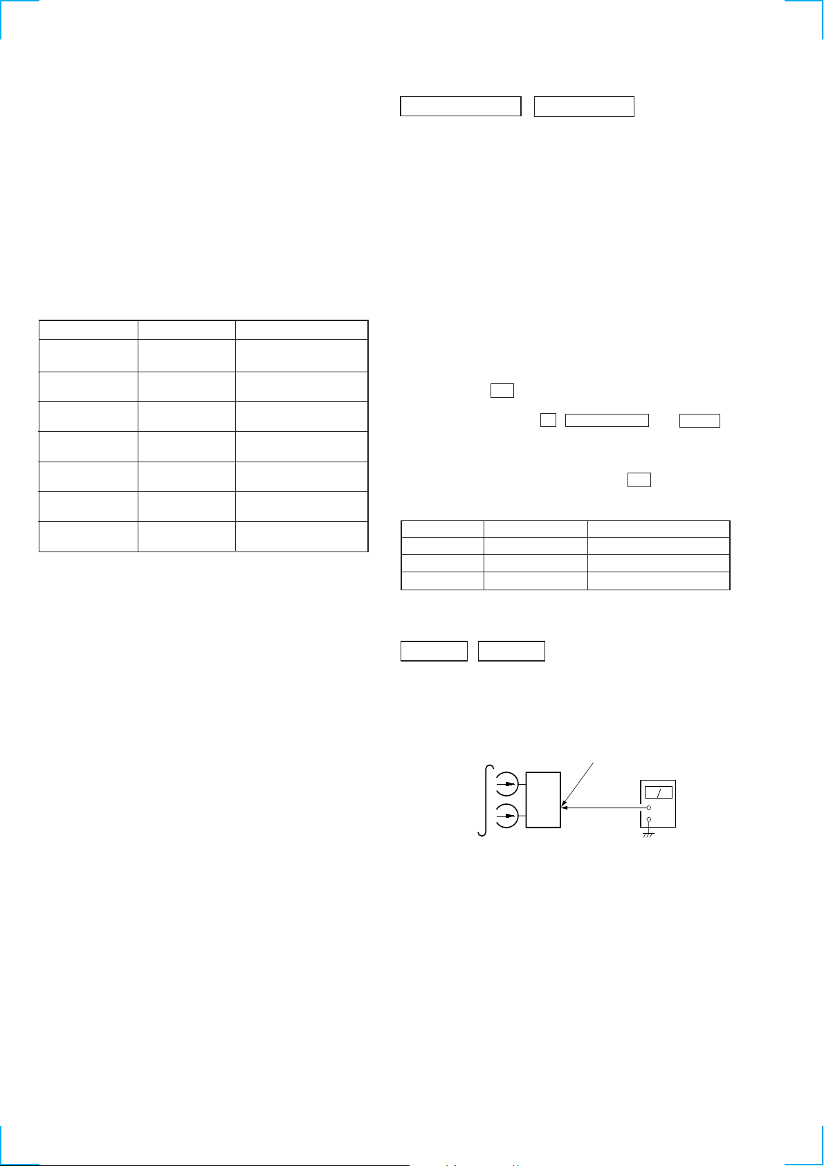
VIDEO SECTION
Frequency Adjustment
Connection:
Procedure:
1. Connect the frequency counter to check point of the VIDEO
board.
2. Turned power switch on.
3. Press the FUNCTION button to select the CD.
4. Adjust CT503 on the VIDEO board so that the frequency counter
reading 27.0 MHz ± 80 Hz at stop status.
Adjustment Location:
VIDEO Board (SIDE B)
A
within 4
±
1 Vp-p
B
7. After check, remove the lead wire connected in step 2 and 3.
Note: • Try to measure several times to make sure than the ratio of A : B
or B : A is more than 10 : 7.
• Take sweep time as long as possible and light up the brightness
to obtain best waveform.
RF Level Check
oscilloscope
BD board
TP (RF)
TP (VC)
+
–
Procedure:
1. Connect oscilloscope to TP (RF).
2. Connect between TP (AGCCON) and TP (GND) by lead wire.
3. Turn the power ON.
4. Load a disc (YEDS-18) and press the ^ button to play.
5. Confirm that the oscilloscope waveform is clear and check RF
signal level is correct or not.
6. After check, remove the lead wire connected in step 2.
Note: Clear RF signal waveform means that the shape “≈” can be clearly
distinguished at the center of the waveform.
level:
1.45
VOLT/DIV: 200 m
TIME/DIV: 500 ns
±
0.3 Vp-p
Checking Location:
BD BOARD (Side B)
TP (AGCCON)
TP (RF)
IC102
TP (TE)
TP (FE)
IC103
TP (VC)
TP (GND)
TP (FE1)
IC101
1717
HCD-VX550
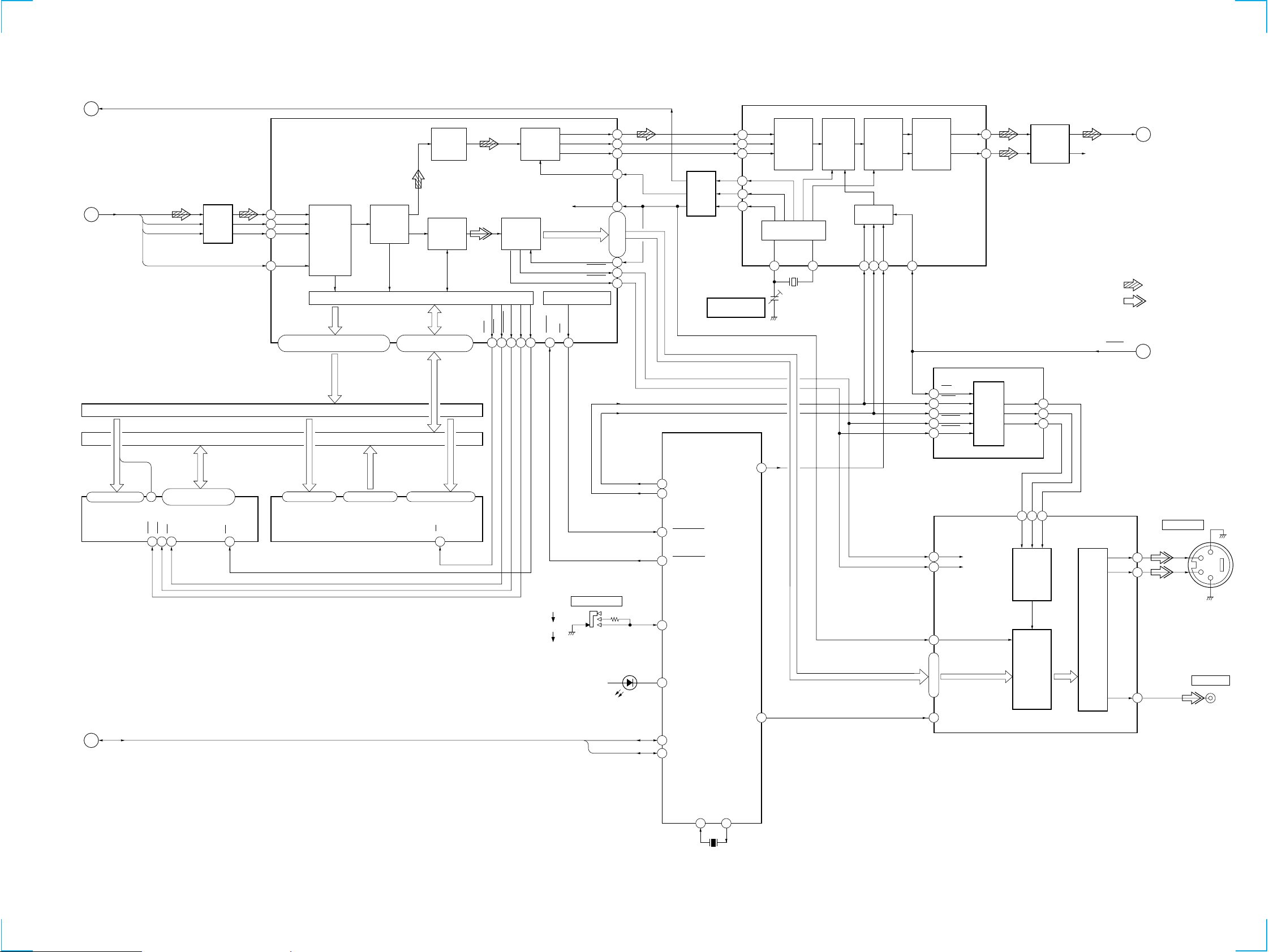
7-1. BLOCK DIAGRAM
CD SERVO SECTION
DETECTOR
A
B
C
D
I-V AMP
F
E
OPTICAL PICK-UP
(KSS-213D/Q-NP)
SECTION 7
DIAGRAMS
LPH
CTL1
FILTER
RF AMP,
A+5V
7
4
2
1
5
10
6
5
6
7
8
10
11
FOCUS/TRACKING ERROR AMP
A
B
C
D
F
F I-V AMP
E
E I-V AMP
IC103
RF
SUMMING
AMP
RF EQ
AMP
FOCUS
ERROR AMP
TRACKING
ERROR AMP
RFO
HOLD SW
16
FE
14
TE
13
LPH
21
DIGITAL SIGNAL PROCESSOR
IC101 (1/2)
RFAC
50
49
48
ASYMMETRY
CORRECTOR
ASYI
ASYO
DIGITAL
CLV
PROCESSOR
MDP
25 76 77
53 55
FILI
PCO
FILO
CLTV
DIGITAL PLL
TO SERVO AUTO
SEQUENCER
CPU INTERFACE
SENSE
DATA
CLOK
XLAT
125254
XPCK
EFM
DEMODULATOR
RAM
INTERNAL BUS
CORRECTOR
SUBCODE
PROCESSOR
EXCK
SCOR
SBSO
SQCK
SQSO
79 801574 6 5 10 111368 3
WFCK
XUGF
GFS
EMPH
32K
ERROR
16 69
C4M
CLOCK
GENERATOR
D/A
DIGITAL
INTERFACE
MUTE
XTSL
DIGITAL
OUT
XTAO
XTAI
PCMD
BCK
LRCK
C2PO
WDCK
DOUT
MD2
XRST
72
71
66
67
65
14
17
64
63
2
IC104
ADATA
D+5V
BCLK
LRCK
C2PO
OPTICAL
TRANSCEIVER
IC381
MCLK
33.8MHz
DATA, BCK,
LRCK, C2PO
CD DIGITAL OUT
OPTICAL
A
B
(Page 19)
(Page 19)
LASER DIODE
2-AXIS
DEVICE
(TRACKING)
(FOCUS)
LDON
22
LD
LD. DRIVER
LD
PD
M101
(SPINDLE)
M102
(SLED)
T+
T–
F+
F–
Q101
FOCUS/TRACKING COIL DRIVE,
SPINDLE/SLED MOTOR DRIVE
+
M
+
M
VO3(+)
17
VO3(–)
18
VO4(+)
15
VO4(–)
16
VO2(+)
12
VO2(–)
11
VO1(+)
14
VO1(–)
13
3
IC102
MOTOR
DRIVE
MOTOR
DRIVE
COIL
DRIVE
COIL
DRIVE
APC LD
AMP
OPIN3(–)
OPIN4(+)
OPIN4(–)
OPIN2(+)
OPIN2(–)
OPIN1(+)
OPIN1(–)
APC PD
AMP
23
27
26
5
6
2
3
PD
4
DIGITAL SERVO
SFDR
29
SRDR
30
TFDR
31
TRDR
32
FFDR
33
FRDR
34
PROCESSOR
IC101 (2/2)
PWM GENERATOR
FOCUS/TRACKING/SLED
40 41 39 43
FE
TE
SE
RFDC
A/D
CONVERTER
FOCUS/
TRACKING/SLED
SERVO DSP
MIRR,
DFCT, FOK
DETECTOR
SERVO
INTERFACE
SERVO AUTO
SEQUENCER
FOK
MIRR
DFCT
COUT
SCLK
3 5 4 1 18 36 37 10
SCOR
SENSE
DSP CLK
DSP DATA
DSP LATCH
LDON
SENSE CLK
28 2
DISC IN DETECT
SENSOR
LEVEL SHIFT
22
20
21
19
8
SUBQ CLK
SUBQ DATA
CD MECHANISM CONTROLLER
IC505 (1/2)
DISC TRAY
SENSOR
IC703
Q701
60 61 71 70 69 68 59
DISC-SENS
TBL-L
TBL-R
65 63 67
IC702
LOAD-OUT
LOAD-IN
66
DISC TRAY SLIDE MOTOR DRIVE
10
2
T-SENS
FIN
RIN
(OPEN/CLOSE DET)
CLOSE
OUT-OPEN
IC801
MOTOR
DRIVE
S801
OPEN
SYSTEM CONTROLLER
IC501 (1/4)
OUT1
7
OUT2
4
DSP MUTE
DEVICE RESET
DISC TRAY
ADDRESS DETECT
ROTARY
ENCODER
S811
4 2 3
ENC1
ENC2
M
(DISC TRAY SLIDE)
CTRL1
CTRL2
XRESET
ENC3
M801
XRST
CTL1
LPH
RESET
C
(Page 19)
11
19
77
12
STBY2STBY1
209
SSTP
26
A+5V
TO CPU INTERFACE
S101
(LIMIT)
DISC TRAY TURN MOTOR DRIVE
3
6
IN1
IN2
IC701
MOTOR
DRIVE
OUT1
OUT2
7
2
M
(DISC TRAY TURN)
M701
• SIGNAL PATH
: CD PLAY
16
: DIGITAL OUT
1818
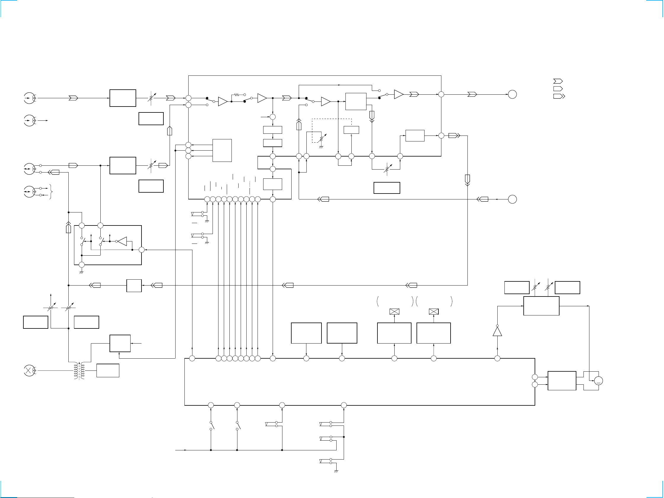
HCD-VX550
AUDIO/VIDEO CD SECTION
MCLK 33.8MHz
A
(Page 18)
DATA, BCK,
B
(Page 18)
LRCK, C2PO
DATA
BCK
LRCK
C2PO
LEVEL
SHIFT
IC501
MPEG VIDEO/AUDIO DECODER,
VIDEO SIGNAL PROCESSOR
IC506
CD-DATA
180
CD-BCK
184
CD-LRCK
182
CD-C2PO
185
100,98,114,116,118,120,121,122,124
ADDRESS BUS
DATA BUS
CD-ROM
INTERFACE
CIRCUIT
MA0 – MA10
104,110,112,111,108,105,102,99,96,
A0 – A18
MPEG
SYSTEM
DECODER
D-RAM/ROM INTERFACE
MD0 – MD15
54,58,60,64,68,72,74,78,
76,73,70,66,62,59,56,53
MPEG
AUDIO
DECODER
MPEG
VIDEO
DECODER
D0 – D15
MCE
128
VIDEO
PROCESS
CIRCUIT
SD-RAS
MWE
82 86 85
AUDIO
INTERFACE
CIRCUIT
SD-CAS
SD-CSO
90
VDATA0 – 7
CPU INTERFACE
INT
RESET
13 16
DA-DATA
DA-BCK
DA-LRCK
DA-XCLK
SYS CLK
VCK-IN
HSYNC
VSYNC
161
167
166
169
178
150,152,154,155
142,143,145,148,
177
157
158
DATA
CLK
OSC
BUFFER
IC510
VIDEO FREQUENCY
CT503
(27MHz)
DATA
18
BCK
17
LRCK
19
768FSO
21
384FSO
20
MCKO
4
INPUT
INTERFACE
CIRCUIT
TIMING CONTROL/
CLOCK GENERATOR
XT2
X503
27MHz
XT1
DIGITAL FILTER,
D/A CONVERTER
DIGITAL
FILTER,
NOISE
SHAPER
CIRCUIT
IC509
D/A
CONVERTER
MODE
CONTROL
MC
MD
9 724 1
8
(Page 21)
R-CH
CD-L
E
• SIGNAL PATH
VOUTL
LOW-PASS
FILER
ML
RSTB
10
VOUTR
14
11
LOW-PASS
FILER
IC515
: CD PLAY (AUDIO)
: CD PLAY (VIDEO)
(Page 18)
RESET
PCL
4
DATA
3
CLK
1
HSYNC
20
VSYNC
19
D/A
V-B
V-G
V-R
18
17
16
C
21 – 24, 27 – 32,20
A0 – A10 BA
D-RAM
IC507
DATA, CLK
D
(Page 22)
A0 – A10
A11
2,3,5,6,8,9,11,12,39,
19
40,42,43,45,46,48,49
RAS
WE
CAS
17 1516
D0 – D15
DQ0 – DQ15
HSY
28
VSY
27
VCLK
51
2
–
8
,
10
NTB
22
D/A CONVERTER
IC511
YUV0 – 7
DIGITAL RGB ENCORDER
IC514
64 157
ROSD
GOSD
OSD
TIMING
CONTROL
Y/C
FILTER
BOSD
D/A
COUT
YOUT
VOUT
J301
S VIDEO OUT
37
45
39
C
Y
1
3
4
2
J302
VIDEO OUT
DF LATCH
A0 – A10
12 – 5, 27, 26, 23
A0 – A10
CS
18
PROGRAM ROM
IC508
D0 – D7
13 – 15, 17 – 21
O0 – O7
A11–A17
25, 4, 28, 29, 3, 2, 30
A11 – A17
CE
22
NTSC
AUTO
PAL
S501
SYSTEM SELECT
(SELF DIAGNOSIS)
I2C CLK
I2C DATA
D502
CLK1
33
DATA1O
31
20
CL680 HINT
24
8830 RESET
CD MECHANISM CONTROLLER
IC505 (2/2)
93
NT/PAL
TEST LED
73
NT/PAL OUT
29
I2C/RX
I2C/TX
30
22
27MHz
VD0 – VD7
21
XOUT
XIN
1315
X501
16
10MHz
1919
HCD-VX550
TAPE DECK SECTION
HP101
(PLAYBACK)
L-CH
R-CH R-CH
HRPE101 (1/2)
(RECORD/PLAYBACK)
L-CH
R-CH R-CH
DECK PROCESS
DECK A/B SELECT, PB/REC EQ AMP,
DOLBY NR AMP, ALC, AMS
IC301
DOLBY PASS
NORM/HIGH
PB A/B
70
120
R-CH
NR ON/OFF
BIAS ON/OFF
RM ON/OFF
L.P.F.
BUFFER
28
27
AMS
CIRCUIT
REC/PB/PASS
LM ON/OFF
26
+
MAOUT
MSIN
MSOUT
RIN (L)
43
ALC (L)
44
DOLBY NR
ALC
ROUT (L)
ALC
35 34
AMP
CIRCUIT
IN (L)
REC OUT (L)
39
RV301
REC LEVEL (L)
(DECK B)
EQ IN (L)
38
PB EQ AMP
(DECK A)
IC611
PB EQ AMP
(DECK B)
IC601
REC/PB SWITCHING
3
1
R-CH
IC602
R-CH
RV311
PB LEVEL (L)
(DECK A)
RV301
PB LEVEL (L)
(DECK B)
4
AIN (L)
48
BIN (L)
46
BIAS (N)
33
BIAS (C)
32
BIAS (M)
31
S1004
(DECK A 120/70)
S1008
(DECK B 120/70)
BIAS
CONTROL
CIRCUIT
B NORM/CROM
ALC ON/OFF
A 120/70
1516182022 23242517
19
REC
EQ AMP
PB OUT (L)
EQ OUT
40
(L)
36
PB-L
REC-L
F
(Page 21)
G
(Page 21)
• SIGNAL PATH
: PLAYBACK (DECK A)
: PLAYBACK (DECK B)
: RECORD
RV441
REC BIAS (R)
(DECK B)
HRPE101 (2/2)
(ERASE)
R-CH
16
2
RV341
REC BIAS (L)
(DECK B)
BIAS OSC
T621
BIAS OSC
Q621, 622
REC BIAS
SWITCH
Q623
C331, L331
BIAS
TRAP
B+
(A+7V)
D+5V
100
TC-RELAY
(DECK A PLAY)
8584838281 807978
PB-A/B
EQ-H/N
ALC-ON/OFF
A-PLAY-SW
87
S1001
S1002
(DECK B PLAY)
BIAS
REC-MUTE
B-PLAY-SW
86
TC-MUTE
R/P-PASS
NR-ON/OFF
(DECK A HALF)
S1003
77
AMS-IN
A-HALF
88
ROTATION
DETECT SENSOR
(DECK A)
IC1001
91
A-SHUT
S1006
(DECK B HALF)
S1005
(DECK A REC)
S1009
(DECK B REC)
ROTATION
DETECT SENSOR
(DECK B)
IC1002
90
B-SHUT
SYSTEM CONTROLLER
B-HALF
89
IC501 (2/4)
TRIGGER PLUNGER
DECK A
TRIGGER
PLUNGER DRIVE
(DECK A)
Q333, 334
73
A-TRG
TRIGGER PLUNGER
DECK B
TRIGGER
PLUNGER DRIVE
(DECK B)
Q331, 332
72
B-TRG
Q335
76
CAP-M-H/L
RV1001
TAPE SPEED
(HIGH)
CAPM-CNT1
CAPM-CNT2
CAPSTAN MOTOR
CONTROL SWITCH
Q1001
75
MOTOR DRIVE
74
RV1002
TAPE SPEED
(NORMAL)
CAPSTAN
Q336 – 343
M
M1
(CAPSTAN)
2020
HCD-VX550
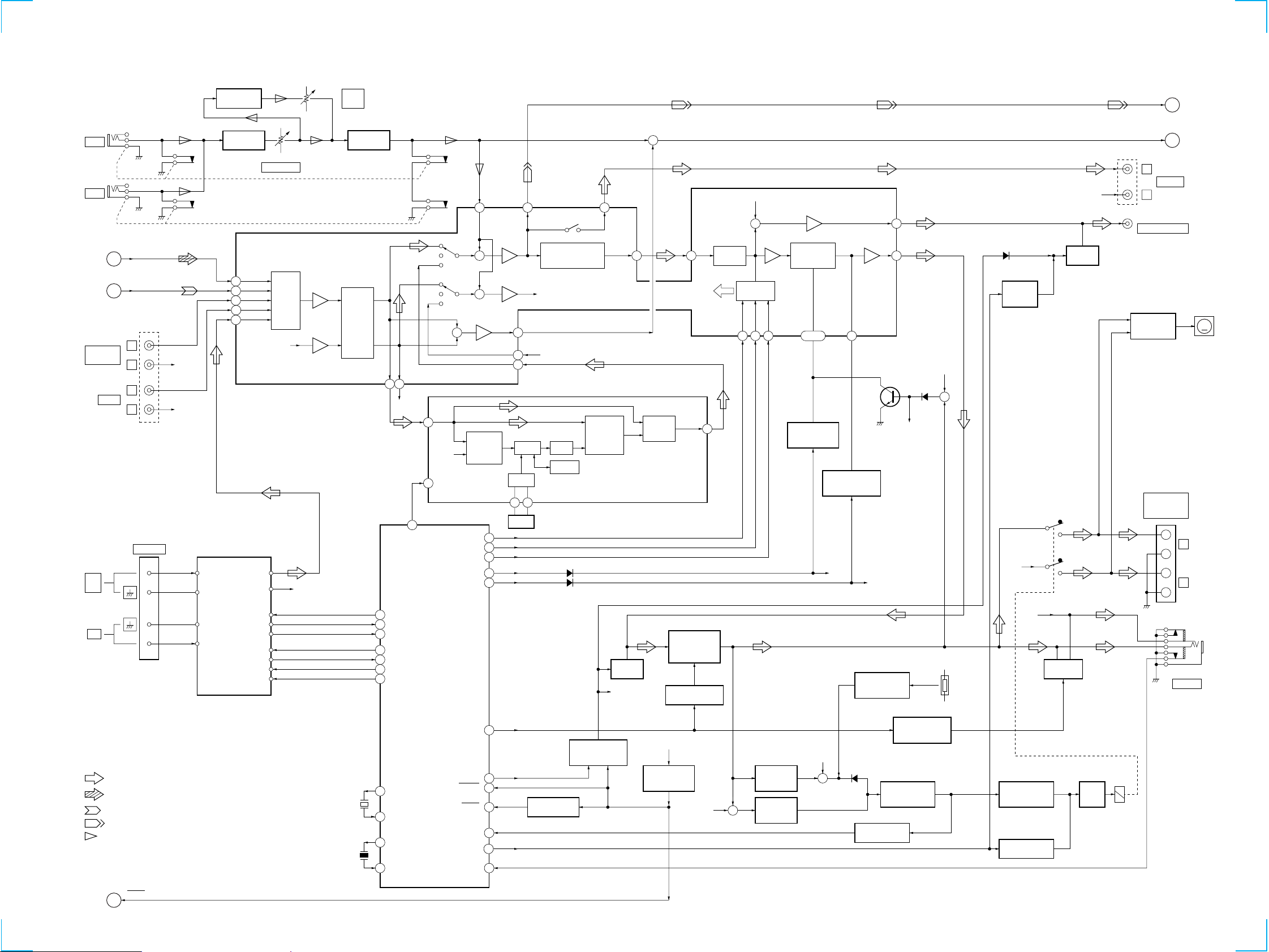
MAIN SECTION
J711
MIC 2
J712
MIC 1
VIDEO
MD IN
CD-L
E
PB-L
F
(Page 19)
(Page 20)
(AUDIO) IN
FM
75Ω
J101 (1/2)
L
R
L
R
ANTENNA
R-CH
R-CH
DIGITAL ECHO
IC711
MIC AMP
IC712 (1/2)
GRAPHIC EQUALIZER CONTROL,
IN E2
65
IN D2
66
IN B2
68
IN A2
69
IN C2
67
FM/AM TUNER UNIT
FM ANT
FM ANT
RV712
MIC LEVEL
INPUT SELECT SWITCH,
ELECTRICAL VOLUME
IC101
INPUT
SELECT
SWITCH
R-CH
ST-L
ST-R
R-CH
RV711
ECHO
LEVEL
MIC AMP
IC712 (2/2)
SOUND
CONTROL
CIRCUIT
KEY IN2
60 5
R-CH
KEY IN1
40
11
R-CH
3
VC L+R/L–R
L-IN
L+R/L–R
493-DATA
493-LATCH
BASS FREQ.
2 58 57
+
493-CLK
DBFB-H/L
MIC IN
+
+
KEY OUT 1
KEY OUT 2
L+R/L–R
MATRIX
CIRCUIT
47
48
38
7
44
L+R
23 24
REC A2
GRAPHIC EQUALIZER
CONTROL CIRCUIT
R-CH
30
6
R-CH
59
ADM L.P.F.
OSC
LC-INELC-INB
OSC
D607
D644
S-RAM
F OUT2
L/R+DELAY
CIRCUIT
REC B2
42 41
+
EFFECT/
BYPASS
SURROUND
PROCESSOR
IC1201
VOL
IN2
COMMAND
L-OUT
14
VOLUME
CONTROL
R-CH
+
CPU
INTERFACE
DATA
CLOCK
LATCH
34
BASS BOOST
CONTROL
CIRCUIT
BB B2,
BB A2
38, 39
DBFB CONTROL
SWITCH
Q111
SUPER
WOOFER
BUF IN2
373233
BASS FREQUENCY
CONTROL SWITCH
Q201
R-CH
BUF
OUT2
FEED BACK
R-CH
72
36
SWITCH
Q112
R-CH
D141
R-CH
+
D191
PROTECT
SWITCH
R-CH
Q192
REC-L
SPEANA
J101 (2/2)
L
R-CH
MUTING
Q191
–1
R
SUPER WOOFER
FAN MOTOR
DRIVE
Q401, 402
USE 8 – 16Ω
G
H
MD OUT
J191
TM401
SPEAKER
IMPEDANCE
(Page 20)
(Page 22)
M501
(FAN)
M
+
L
–2
–
+
R
–
AM
• SIGNAL PATH
: TUNER (FM/AM)
: CD PLAY
: TAPE PLAY
: RECORD
: MIC INPUT
(Page 22)
I
RESET
AM ANT
AM ANT
ST-MUTE
STEREO
TUNED
ST-DIN
ST-DOUT
ST-CLK
ST-CE
49
ST-MUTE
STEREO
50
TUNED
51
ST-DOUT
53
54
ST-DIN
ST-CLK
55
ST-CE
52
SYSTEM CONTROLLER
IC501 (3/4)
AC-CUT
RESET
F-RELAY
RY-SW
1
MUTING CONTROL
6
22
12
27
3
36
RESET SWITCH
Q501
STK-MUTE
LINE-MUTE
XC-OUT
X601
32.768kHz
X613
16MHz
16
11
XC-IN
10
13
X-OUT
X-IN
15
PROTECTOR
SWITCH
Q508, 509
MUTING
Q113
R-CH
POWER AMP
STANDBY SWITCH
Q803, 804, 881
+5V
RESET SIGNAL
GENERATOR
IC502
IC801
R-CH
TH831
TEMPERATURE
DETECT SWITCH
Q831, 832
MUTING CONTROL
SWITCH
Q412
R-CH
OVER LOAD
DETECT
Q801
DC DETECT
+
SWITCH
Q433, 434
D803
+
PROTECT SWITCH
OVER LOAD
DETECT SWITCH
Q439
Q432
R-CH
OVER LOAD
DETECT SWITCH
Q437
PROTECT SWITCH
Q435, 436
MUTING
Q411, 471
RELAY
DRIVE
Q431
J701
PHONES
RY401
2121
HCD-VX550
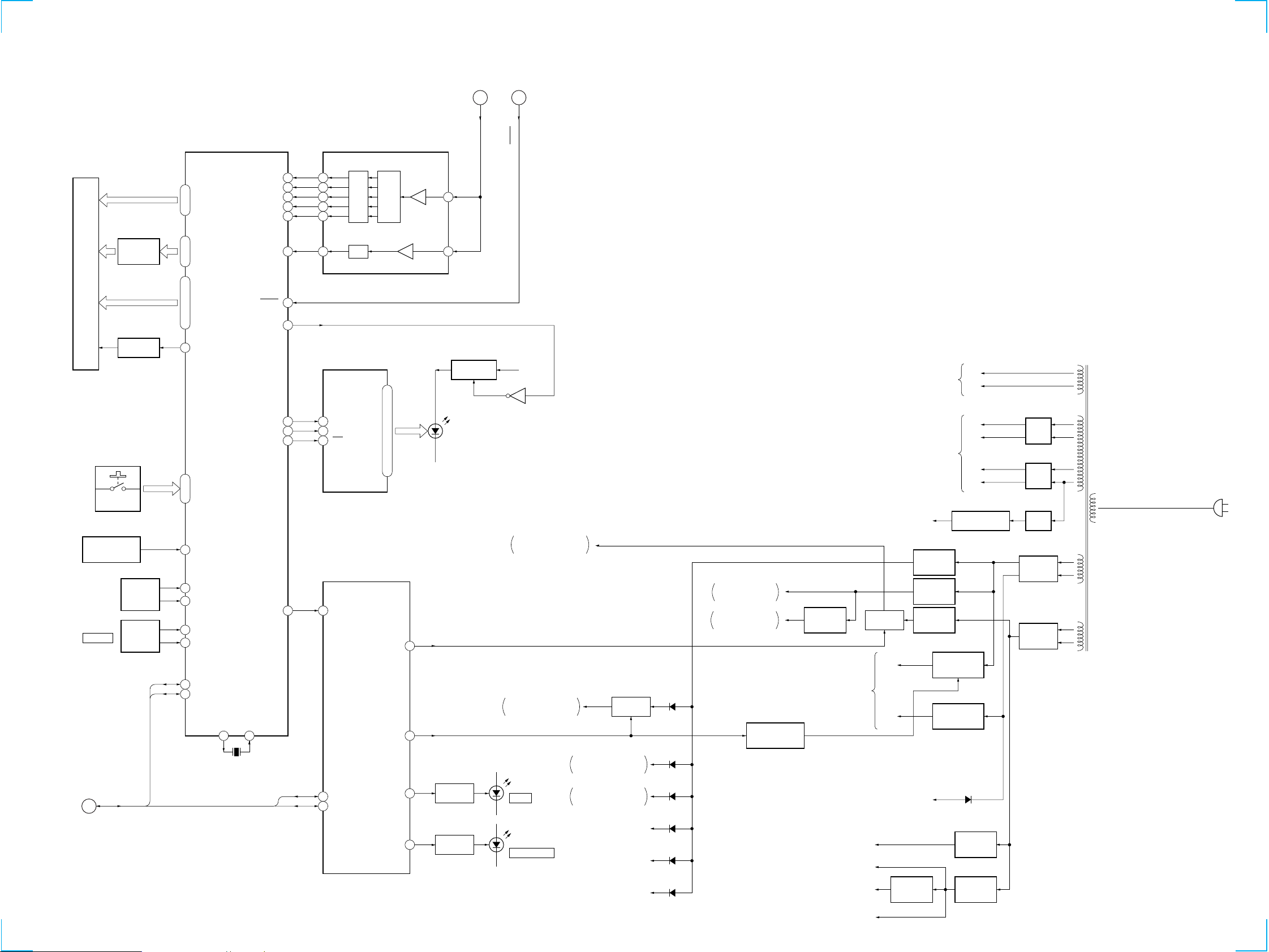
DISPLAY/KEY CONTROL/POWER SUPPLY SECTION
GRID DRIVE
Q607 – 612
FL601
FLUORESCENT INDICATOR TUBE
GRID DRIVE
Q613
FLUORESCENT INDICATOR TUBE DRIVER,
45
KEY CONTROL
46 – 67
S1 – S22
32 – 27
G13 – G18
G2 – G12
44 – 42, 40 – 33
G1
IC601
S LOW FREQ (BPF0)
BPF1
BPF2
BPF3
BPF4
ALL BAND (L+R)
RESET
L SEL
16
17
18
19
20
21
73
7
17
16
14
13
12
11
F01
F02
F04
F05
F06
L+R
LED DRIVER
IC604
DET
DET
BAND-PASS FILTER
IC603
B.P.F.
LINE
REC IN
(Page 21)(Page 21)
H
SPEANA
IN
4
6
B+ SWITCH
Q601, 602
Q603
I
RESET
+5V (LED)
TO FLUORESCENT
INDICATOR TUBE
(FL601)
VF1
VF2
POWER TRANSFORMER
T951
S611 – 630, 632 – 635,
S638 – 651, 751 – 757
REMOTE CONTROL
RECEIVER
IC602
S601
(JOG DIAL)
S602
VOLUME
DATA, CLK
D
(Page 19)
16
ROTARY
ENCODER
S601
ROTARY
ENCODER
S602
11 – 14
1
2
8
9
10
78
79
KEY0 – KEY3
SIRCS
JOG-A
JOG-B
VOL-A
VOL-B
I2C DATA
I2C CLK
XOUT
72 70
X601
12.5MHz
LED DATA
LED SCK
LED LAT
WAKE UP
XIN
5
3
4
22
DATA
13
14
CLK
15
STB
SYSTEM CONTROLLER
IC501 (4/4)
WAKE UP
18
30
IIC-DATA
29
IIC-CLK
P1 – P9, P11, P12, P15, P16
17, 19 – 23, 1 – 3, 5, 7, 10, 11
POWER
5
2
39
26
CD-POWER
STBY LED
TIMER LED
D611 – 624,
D627 – 631,
D751 – 753
LED DRIVE
Q604, 605
LED DRIVE
Q606
A+5V (SW)
D/A CONVERTER (IC509),
VIDEO AMP CIRCUIT B+
D+5V (SW)
M62493FP (IC101),
CD SENSOR CIRCUIT B+
D754
I/u
D632
TIMER SELECT
B+ SWITCH
Q904, 905
+5V
SYSTEM CONTROLLER
(IC501) B+
+5V
CD MECHANISM
CONTROLLER (IC505) B+
+5V (STBY)
(PANEL SECTION B+)
D+5V (UNSW)
(TAPE DECK SECTION B+)
+5V (LED)
(PANEL SECTION B+)
D923
D501, 502
D507
D509
D922
D924
D+5V (SW)
CD SERVO/VIDEO CD
SECTION B+
+3.3V
MPEG VIDEO/AUDIO
DECODER (IC506) B+
REGULATOR
CONTROL SWITCH
Q903, 923
+3.3V
REGULATOR
IC504
TC, PANEL,
AUDIO
CD M+7V
(CD MOTOR SECTION B+)
TC M+12V
(TC MOTOR SECTION B+)
ST +10V
(FM/AM TUNER UNIT B+)
CD M+12V
(CD MOTOR SECTION B+)
POWER AMP (IC801),
PROTECTOR CIRCUIT
–26V
(FL DRIVER (IC601) B–)
REGULATOR
REGULATOR
B+ SWITCH
Q911, 912
A+7V
A–7V
REGULATOR
FAN MOTOR B–
+10V
REGULATOR
Q909
+5V
IC902
+5V
IC101
+5V
IC904
REGULATOR
Q901, 902, 913
REGULATOR
Q914, 951, 952
+VL
–VL
+VH
–VH
–26V REGULATOR
Q971
+7V
–7V
D405 – 407
+7V
REGULATOR
IC901
+12V
REGULATOR
IC903
RECT
D832
RECT
D831
RECT
D971
RECT
D901 – 904
RECT
D907 – 910
AC IN
2222
HCD-VX550
CD SW board
TRANS board
MAIN board
PANEL board
TUNER (FM/AM)
SURROUND board
VIDEO board
5V POWER board
CONNECTOR board
SENSOR board
MOTOR (TURN) board
MOTOR (SLIDE) board
LEAF SW board
AUDIO board
BD board
THIS NOTE IS COMMON FOR PRINTED WIRING BOARDS AND SCHEMATIC DIAGRAMS.
(In addition to this, the necessary note is printed in each block.)
Note on Printed Wiring Board:
• X : parts extracted from the component side.
• p : parts mounted on the conductor side.
• b : Pattern from the side which enables seeing.
(The other layers' patterns are not indicated.)
Caution:
Pattern face side: Parts on the pattern face side seen from
(Side B) the pattern face are indicated.
Parts face side: Parts on the par ts face side seen from
(Side A) the parts face are indicated.
• Indication of transistor.
C
Q
B
E
B
B
These are omitted.
Q
CE
These are omitted.
Q
CE
These are omitted.
Note on Schematic Diagram:
• All capacitors are in µF unless otherwise noted. pF: µµF
50 WV or less are not indicated except for electrolytics
and tantalums.
• All resistors are in Ω and 1/
specified.
¢
•
• 2 : nonflammable resistor.
• 5 : fusible resistor.
• C : panel designation.
• U : B+ Line.
• V : B– Line.
• H : adjustment for repair.
• Voltages are taken with a VOM (Input impedance 10 MΩ).
• Waveforms are taken with a oscilloscope.
• Circled numbers refer to waveforms.
• Signal path.
: internal component.
The components identified by
mark ! or dotted line with mark
! are critical for safety.
Replace only with part number
specified.
Voltage variations may be noted due to normal production tolerances.
Voltage variations may be noted due to normal production tolerances.
F : TUNER (FM/AM)
E : PLAYBACK (DECK A)
d : PLAYBACK (DECK B)
G : RECORD
L : CD PLAY (VIDEO)
J : CD PLAY (AUDIO)
c : DIGITAL OUT
N : MIC INPUT
4
7-2. CIRCUIT BOARD LOCATION
W or less unless otherwise
2323

HCD-VX550
7-3. PRINTED WIRING BOARD BD BOARD • Refer to page 23 for Circuit Boards Location.
(Page 28)
2424
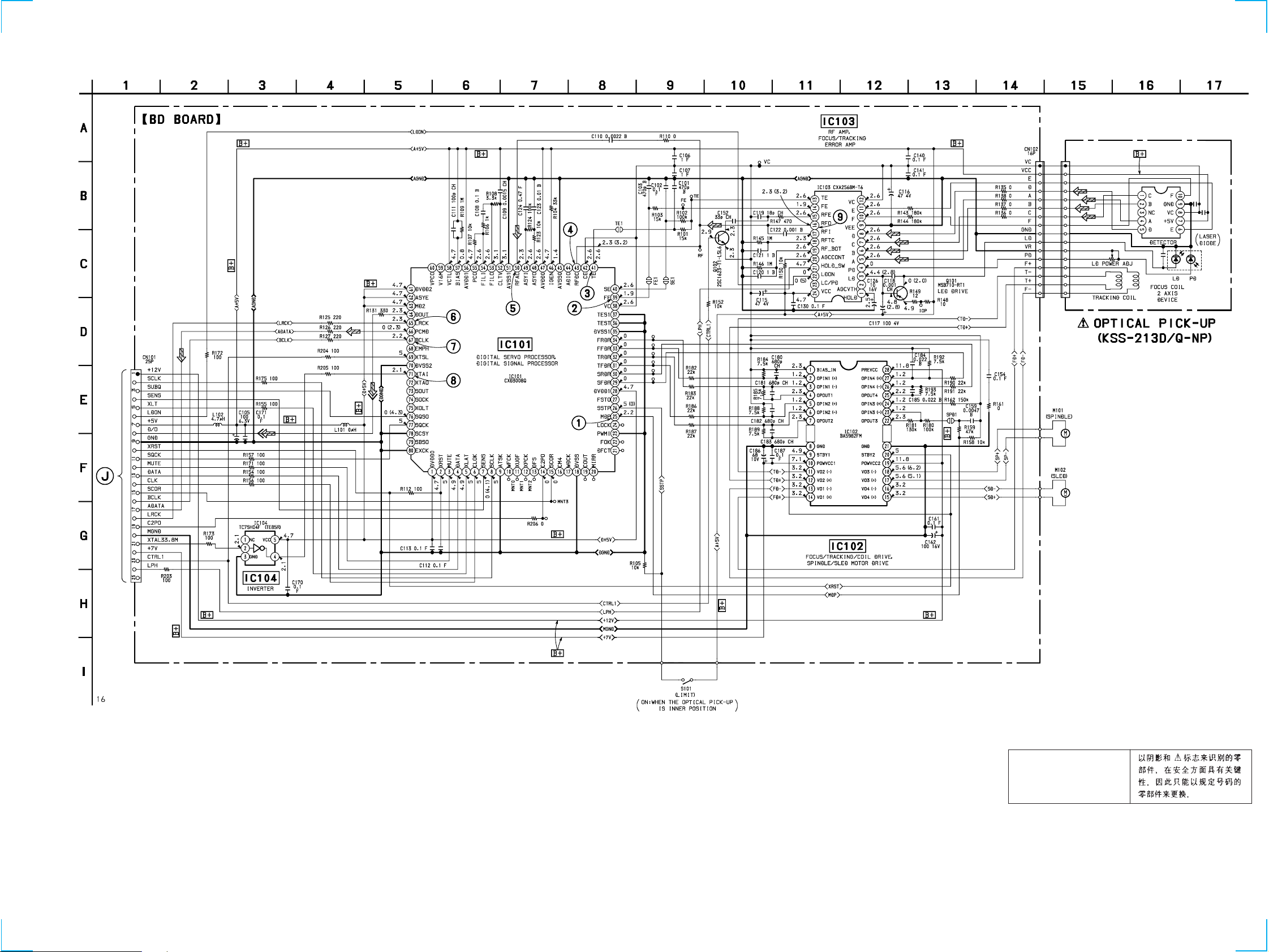
7-4. SCHEMATIC DIAGRAM BD BOARD • Refer to page 29 for Waveforms. • Refer to page 45, 46 for IC Block Diagrams.
HCD-VX550
(Page 26)
• Voltages and waveforms are dc with respect to ground
under no-signal conditions.
no mark : CD STOP
( ) : CD PLAY
The components identified by
mark ! or dotted line with mark
! are critical for safety.
Replace only with part number
specified.
2525
 Loading...