

Sony HCD V8800 Service Manual
HCD-V8800
SERVICE MANUAL
HCD-V8800 is the tuner, deck, Video CD and
amplifier section in LBT-V8800AV.
Model Name Using Similar Mechanism HCD-V4500
CD
SECTION
TAPE
DECK
SECTION
CD Mechanism Type CDM37L-5BD21AL
Base Unit Type BU-5BD21AL
Optical Pick-up Type KSS-213D/Q-NP
Model Name Using Similar Mechanism HCD-V4500
T ape Transport Mechanism Type TCM-220WR2
E Model
Chinese Model
SPECIFICA TIONS
— Continued on next page —
MICROFILM
COMPACT DISC DECK RECEIVER
— 1 —
CAUTION
Use of controls or adjustments or performance of procedures
other than those specified herein may result in hazardous radiation exposure.
Notes on chip component replacement
• Never reuse a disconnected chip component.
• Notice that the minus side of a tantalum capacitor may be
damaged by heat.
Flexible Circuit Board Repairing
• Keep the temperature of soldering iron around 270˚C
during repairing.
• Do not touch the soldering iron on the same conductor of the
circuit board (within 3 times).
• Be careful not to apply force on the conductor when soldering
or unsoldering.
Laser component in this product is capable of emitting radiation
exceeding the limit for Class 1.
This appliance is classified as
a CLASS 1 LASER product.
The CLASS 1 LASER PRODUCT MARKING is located on
the rear exterior.
This caution
label is located
inside the unit.
MODEL IDENTIFICA TION
— BACK P ANEL —
MODEL
E, SP model
MY model
CH model
IA model
SAFETY -RELA TED COMPONENT WARNING !!
COMPONENTS IDENTIFIED BY MARK ! OR DOTTED LINE
WITH MARK ! ON THE SCHEMA TIC DIAGRAMS AND IN
THE PAR TS LIST ARE CRITICAL TO SAFE OPERATION.
REPLACE THESE COMPONENTS WITH SONY PARTS
WHOSE PART NUMBERS APPEAR AS SHOWN IN THIS
MANUAL OR IN SUPPLEMENTS PUBLISHED BY SONY .
PARTS No.
4-992-220-0
4-992-220-1
4-992-220-2
4-992-220-3
• Abbreviation
SP : Singapore model
MY : Malaysia model
IA : Indonesian model
CH : Chinese model
— 2 —

NOTES ON HANDLING THE OPTICAL PICK-UP BLOCK
OR BASE UNIT
The laser diode in the optical pick-up block may suffer electrostatic
break-down because of the potential difference generated by the
charged electrostatic load, etc. on clothing and the human body.
During repair, pay attention to electrostatic break-down and also
use the procedure in the printed matter which is included in the
repain parts.
The flexible board is easily damaged and should be handled with
care.
NOTES ON LASER DIODE EMISSION CHECK
The laser beam on this model is concentrated so as to be focused on
the disc reflective surface by the objective lens in the optical pickup block. Therefore, when checking the laser diode emission, observe from more than 30 cm away from the objective lens.
LASER DIODE AND FOCUS SEARCH OPERATION
CHECK
Carry out the “S curve check” in “CD section adjustment” and check
that the S curve waveform is output three times.
T ABLE OF CONTENTS
1. SERVICING NOTE
.......................................................... 4
2. GENERAL .......................................................................... 6
3. DISASSEMBL Y
3-1. Front Panel ........................................................................... 7
3-2. Main Board ........................................................................... 8
3-3. Tape Mechanism Deck.......................................................... 8
3-4. Cassette Lid Assembly.......................................................... 9
3-5. CD Lid Assembly.................................................................. 9
3-6. CD Mechanism Deck .......................................................... 10
3-7. Base Unit ........................................................................... 10
3-8. Disc T able ........................................................................... 10
4. TEST MODE .............................................................. 11
5. MECHANICAL ADJUSTMENTS ...........................12
6. ELECTRICAL ADJUSTMENTS ............................... 12
7. DIAGRAMS
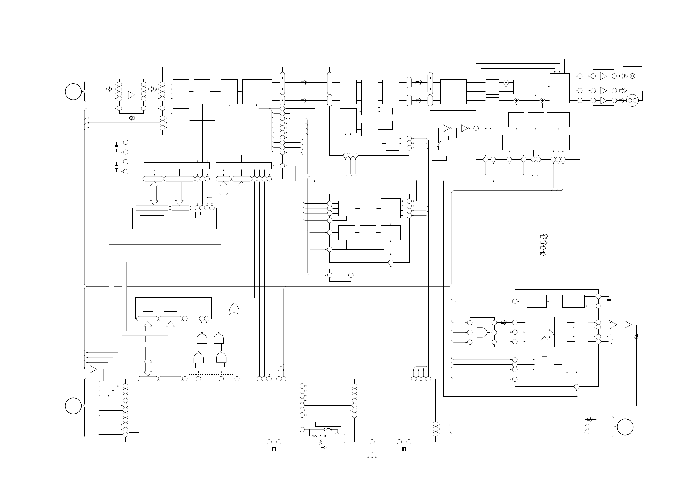
7-1. Circuit Boards Location ...................................................... 17
7-2. Block Diagrams
• KEY CON Section........................................................... 18
• CD Section ....................................................................... 19
• Video Section................................................................... 21
• Deck Section .................................................................... 23
• Main Section .................................................................... 25
• Power Section .................................................................. 27
7-3. Printed Wiring Board — CD Section —............................. 29
7-4. Schematic Diagram — CD Section — ............................... 31
7-5. Schematic Diagram — Video Section — ........................... 33
7-6. Printed Wiring Board — Video Section —......................... 37
7-7. Printed Wiring Board — Main Section —.......................... 40
7-8. Schematic Diagram — Main Section — ............................ 43
7-9. Schematic Diagram — Deck Section — ............................ 47
7-10. Printed Wiring Board — Deck Section — ....................... 51
7-11. Schematic Diagram — Panel Section — ......................... 54
7-12. Printed Wiring Board — Panel Section —....................... 57
7-13. Schematic Diagram — Power Section — ........................ 61
7-14. Printed Wiring Board — Power Section — ..................... 65
7-15. Schematic Diagram — CD Motor Section —.................. 68
7-16. Printed Wiring Board — CD Motor Section —............... 69
7-17. Schematic Diagram — KEY CON Section —................. 71
7-18. Printed Wiring Board — KEY CON Section — .............. 72
7-19. IC Block Diagrams ........................................................... 73
7-20. IC Pin Functions ............................................................... 80
8. EXPLODED VIEWS
8-1. Case and Back Panel Section .............................................. 97
8-2. Front Panel Section 1 .......................................................... 98
8-3. Front Panel Section 2 .......................................................... 99
8-4. Chassis Section ................................................................. 100
8-5. TC Mechanism Section-1 (TCM-220WR2) ..................... 101
8-6. TC Mechanism Section-2 (TCM-220WR2) ..................... 102
8-7. TC Mechanism Section-3 (TCM-220WR2) ..................... 103
8-8. CD Mechanism Section (CDM37L-5BD21AL) ............... 104
8-9. Base Unit Section (BU-5BD21AL) ..................................105
9. ELECTRICAL P ARTS LIST ...................................... 106
— 3 —

SECTION 1
SERVICING NOTE
MC Cold Reset
• The cold reset clears all data including preset data stored in the
RAM to initial conditions. Execute this mode when returning the
set to the customer.
Procedure:
1. Press three buttons SPECTRUM ANALYZER , ENTER , and
DISC 1 simultaneously.
2. The fluorescent indicator tube becomes blank instantaneously,
and the set is reset.
CD Delivery Mode
• This mode moves the pick-up to the position durable to vibration.
Use this mode when returning the set to the customer after repair.
Procedure:
1. Press POWER button to turn the set ON.
2. Press PLA Y MODE button and POWER button simultaneously .
3. A message “LOCK” is displayed on the fluorescent indicator
tube, and the CD delivery mode is set.
MC Hot Reset
• This mode resets the set with the preset data kept stored in the
memory. The hot reset mode functions same as if the power cord
is plugged in and out.
Procedure:
1. Press three buttons SPECTRUM ANALYZER , ENTER , and
DISC 2 simultaneously.
2. The fluorescent indicator tube becomes blank instantaneously,
and the set is reset.
Sled Servo Mode
• This mode can run the CD sled motor freely. Use this mode, for
instance, when cleaning the pick-up.
Procedure:
1. Select the function “CD”.
2. Press three buttons SPECTRUM ANALYZER , ENTER , and
FUNCTION simultaneously.
3. The Sled Servo mode is selected, if “CD” is blanking on the
fluorescent indicator tube.
4. With the CD in stop status, press ) button in CD section to
move the pick-up to outside track, or 0 button to inside track.
5. To exit from this mode, perform as follows:
1) Move the pick-up to the most inside track.
2) Press three buttons in the same manner as step 2.
Note:
• Always move the pick-up to most inside track when exiting from
this mode. Otherwise, a disc will not be unloaded.
• Do not run the sled motor excessively, otherwise the gear can be
chipped.
Change-over of FUNCTION Name
• The FUNCTION name of external input terminal can be changed
over to VIDEO or MD. With the FUNCTION selected to “MD”,
about 5dB mute is applied to the input gain.
Procedure:
1. Press POWER button to turn the set OFF.
2. Press POWER button together with FUNCTION button, and
the power is turned on, the display of fluorescent indicator tube
changes to “MD” or “VIDEO” instantaneously, and thus the
FUNCTION is changed over.
Change-over of AM T uner Step between 9kHz and 10kHz
• A step of AM channels can be changed over between 9kHz and
10kHz.
Procedure:
1. Press POWER button to turn the set ON.
2. Select the function “TUNER”, and press TUNER/BAND but-
ton to select the BAND “AM”.
3. Press POWER button to turn the set OFF.
4. Press ENTER/NEXT and POWER buttons simultaneously,
and the display of fluorescent indicator tube changes to “AM
9k STEP” or “AM 10k STEP”, and thus the channel step is
changed over.
LED and Fluorescent Indicator T ube All Lit, Key Check
Mode
Procedure:
1. Press three buttons SPECTRUM ANALYZER , ENTER , and
DISC 3 simultaneously.
2. LEDs and fluorescent indicator tube are all turned on.
Press DISC 2 button, and the key check mode is activated.
3. In the key check mode, the fluorescent indicator tube displays
“K 1 V0 J0”. Each time a button is pressed, “K”value increases.
However, once a button is pressed, it is no longer taken into
account.
“J” Value increases like 1, 2, 3 ... if rotating JOG knob in “+”
direction, or it decreases like 0, 9, 8 ... if rotating in “–” direction.
“V” V alue increases like 1, 2, 3 ... if rotating VOLUME knob in
“+” direction, or it decreases like 0, 9, 8 ... if rotating in “–”
direction.
4. To exit from this mode, press three buttons in the same manner
as step 1, or disconnect the power cord.
Aging Mode
This mode can be used for operation check of CD section and tape
deck section.
• If an error occurred:
The aging operation stops.
• If no error occurs:
The aging operation continues repeatedly.
1. Aging Mode in CD Section
1-1. Operating procedure of Aging Mode
1. Set discs in DISC 1 and DISC 3 trays.
2. Select the function “CD”.
3. Press three buttons SPECTRUM ANALYZER , ENTER ,
and KARAOKE PON/MPX simultaneously.
4. The aging mode is activated, if a roulette mark on the fluo-
rescent indicator tube is blinking.
5. In the aging mode, the aging is executed in a sequence given
in “1-2. Operation during Aging Mode”.
The aging continues unless an alarm occurred.
6. To exit from the aging mode, press POWER button to turn
the set OFF.
• If a button other than buttons In CD section is pressed during
aging, the aging in the CD section is finished.
• To execute aging to the tape deck section successively, press ·
button in the deck A.
“AGING” is displayed on the fluorescent indicator tube. (For the
aging in tape deck, see “2. Aging Mode in Tape Deck Section”.
1-2. Operation during aging Mode
In the aging mode, the program is executed in the following sequence.
1. The disc tray turns to select a disc. (For a disc selection se-
quence, see Section 1-3.)
2. TOC of disc is read.
3. The pick-up accesses to the last track.
4. Steps 1 through 3 are repeated.
1-3. Disc Selection Sequence
• During the aging mode, discs are selected in the following se-
quence:
Disc 1 → Disc 3
↑↓
Disc 3 ← Disc 1
— 4 —
2. Aging Mode in Tape Deck Section
L
g
H
L
2 time blinking
e
D701
IC771
2-1. Operating procedure of Aging Mode
1. Load a commercially available 10-minute tape into the decks
A and B respectively.
(If a 10-minute tape is not available, another tape may be
used but a cycle time will be longer.)
2. Select the function “TAPE”.
3. Rewind tapes in advance by pressing 0 button respectively on decks A and B.
4. Press three buttons SPECTRUM ANAL YZER , ENTER ,
and KARAOKE PON/MPX simultaneously.
5. Press · button on deck A. (This button triggers the aging
mode.)
6. The aging mode is activated if “AGING A” is displayed on
the fluorescent indicator tube.
7. In the aging mode, the aging is executed in a sequence given
in “2-2. Operation during Aging Mode”.
The aging continues unless an alarm occurred.
8. To exit from the aging mode, press POWER button to turn
the set OFF.
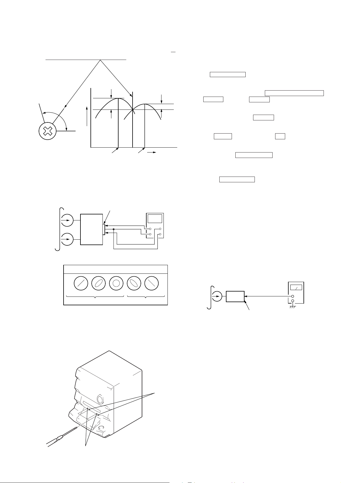
SELF-DIAGNOSIS
This model has the self-diagnosis function for the VIDEO and
AUDIO decoder sections.
Immediately after the power on, the self-diagnosis function searches
each operation of IC’s around the mechanism control microcomputer (IC701).
The results can be checked by connecting an oscilloscope to TP709
(LED) of the VIDEO board.
Oscilloscope (Waveform)
H
Symptom
No error
Light
L
H
External SRAM (IC751)
error
1 time blinking
2-2. Operation during Aging Mode
In the aging mode, the program is executed in the following sequence.
1. A tape on FWD side is played for one minute.
2. PAUSE STOP is made.
3. Recording is made for 3 minutes. (For the deck not having
the record function, the play is executed.)
4. FF is executed up to the end of tape.
5. A tape is reversed, and the tape on REV side is played for
one minute.
6. PAUSE STOP is made.
7. Recording is made for 3 minutes. (For the deck not having
the record function, the play is executed.)
8. FF is executed up to the end of tape.
9. Steps 1 through 8 are executed for the other deck.
10. Steps 1 through 9 are repeated unless an alarm occurred.
2-3. Deck Selection Sequence
• During the aging mode, decks are selected in the following sequence:
Deck A (FWD) → Deck A (REV)
↑↓
Deck B (REV) ← Deck B (FWD)
MPEG decoder (IC201)
error
H
DRAM (IC251) error
3 time blinkin
VIDEO board
TP709 (LED)
L
oscilloscop
+
–
Note: The LED for check (D701) is mounted to some sets
(FORMER TYPE). In this case, confirm the lighting condition of LED.
[VIDEO BOARD] (SIDE A)
[VIDEO BOARD] (SIDE B)
TP709 (LED)
IC751
— 5 —
X901
IC251
Front Panel
SECTION 2
GENERAL
%¡
%º
!∞
!¢
!£
!™
!¡
#¶
#§
#∞
#¢
12
#£
34
!¶!§
#¡ #º @ª @• @¶
#™
!•
!ª
5
6
@º
@§
78
@¡
9
0
@™
@£
@¢
@∞
#•
#ª
$ª
$•
$¶
&™
&¡
&º
^ª
^•
$§
%¶
$º
$¡
$™
$£
$¢$∞
%•
%™
%£
%¢
%∞
%§
^º
%ª
^¡
^¶ ^§ ^∞
^¢
— 6 —
^£
^™
LOCA TION OF PARTS AND CONTROLS
1 POWER button
2 DISPLAY/DEMO button
3 SPECTRUM ANALYZER button
4 Display Window
5 ENTER/NEXT button
6 TUNER MEMORY button
7 TUNING MODE button
8 TUNER/BAND button
9 TUNING (+/–) button
!º STEREO/MONO button
!¡ SLEEP button
!™ DAILY 2 button
!£ DAILY 1 button
!¢ t/CLOCK SET button
!∞ REC button
!§ WAVE button
!¶ DSP button
!• Equalizer indicators
!ª PRO LOGIC button
@º EFFECT button
@¡ GROOVE button
@™ FUNCTION button
@£ VOLUME control
@¢ SUPER WOOFER button
@∞ SUPER W MODE button
@§ GEQ control buttons
@¶ GEQ CONTROL button
@• ENTER button
@ª P FILE MEMORY button
#º # button
#¡ KEY CONTROL indicator
#™ ˜ button
#£ KARAOKE PON/MPX button
#¢ PHONES jack
#∞ ECHO LEVEL knob
#§ MIC 1, MIC 2 jacks
#¶ MIC LEVEL knob
#• Deck B ª, · button
#ª Deck B 0, ) button
$º Deck B r REC button
$¡ Deck B P button
$™ CD SYNC button
$£ Deck B 6 EJECT button
$¢ H SPEED DUB button
$∞ Deck B p button
$§ Deck A 0, ) button
$¶ Deck A 6 EJECT button
$• DOLBY NR button
$ª DIRECTION button
%º Deck A p button
%¡ Deck A ª, · button
%™ 6 OPEN button
%£ CD · button
%¢ CD p button
%∞ CD P button
%§ DISC SKIP button
%¶ CD FLASH button
%• 1/ALL DISCS button
%ª PLAY MODE button
^º CD 0, ) button
^¡ REPEAT button
^™ ≠ AMS ± dial
^£ EDIT button
^¢ NEXT button
^∞ AUTO PBC indicator
^§ PREV button
^¶ PBC indicator
^• ˆ RETURN button
^ª VCD indicator
&º CD LOOP button
&¡ CD NON-STOP button
&™ DISC1-DISC5 buttons
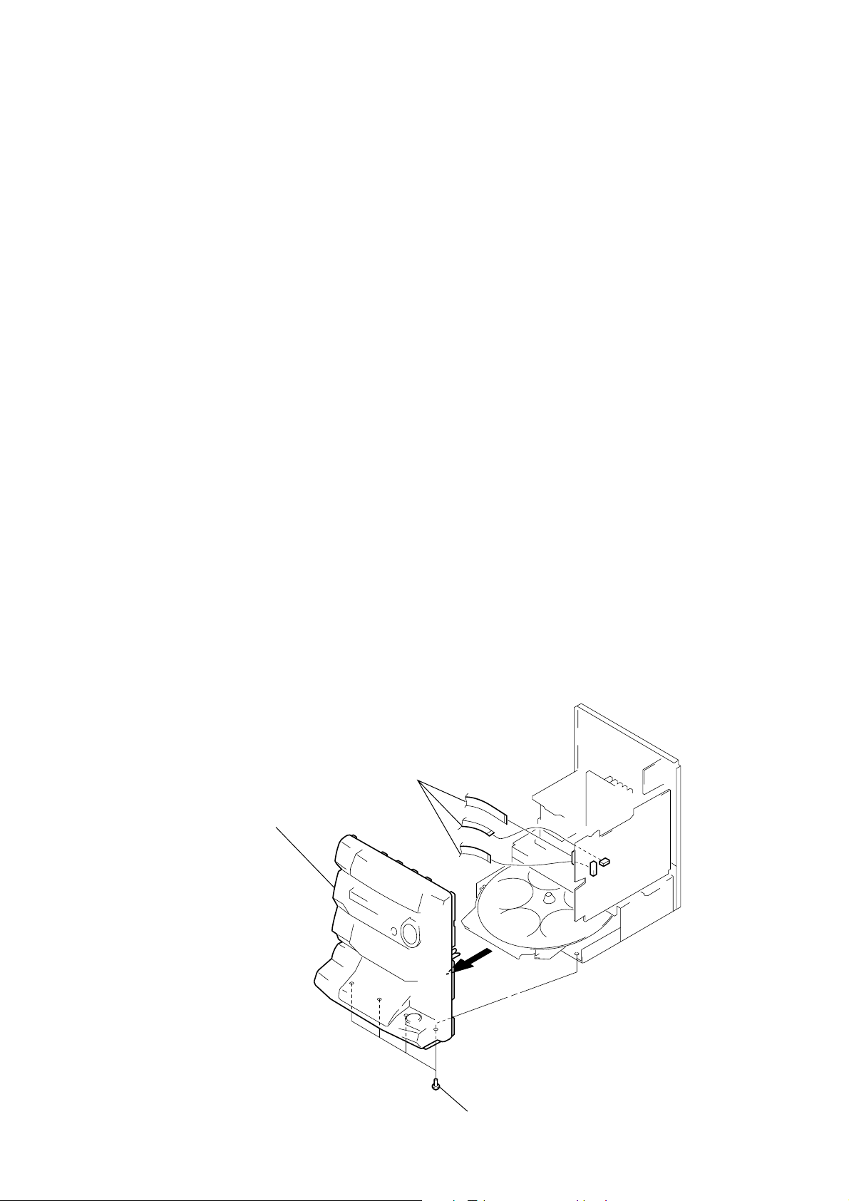
SECTION 3
DISASSEMBL Y
Note: Follow the disassembly procedure in the numerical order given.
3-1. FRONT P ANEL
1
Three flat type wires
(CN401, CN402, CN701)
3
Front panel
2
— 7 —
Four screws (BVTP3x8)
3-2. MAIN BOARD
9
Connector
(CN601)
0
Connector
(CN9001)
4
Power cord
5
Back panel
3
Seven screws (BVTP3x8)
2
Eleven screws
(BVTP3x8)
1
Flat type wire (CN1)
Installing the power cord for the
Chinese model.
Power transformer
Bushing cord
Ferrite core
Wire clamp
!£
MAIN board
6
Connector
(CN961)
7
Flat type wire
(CN801)
3-3. T APE MECHANISM DECK
3
Three screws
(BVTP2.6x8)
A
!¡
Two screws
(BVTP3x8)
4
Three screws (BVTP2.6x8)
5
Remove the tape mechanism deck
section to direction of the arrow
!™
Connector
(CN901)
8
Connector
(CN830)
2
A
.
Open the cassette lids.
1
Push the two buttons.
— 8 —
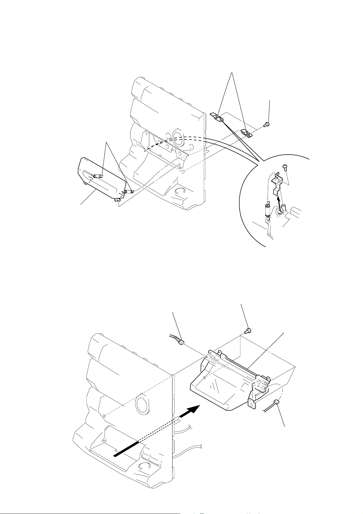
3-4. CASSETTE LID ASSEMBL Y
1
Two springs
4
Cassette lid assembly
3
Two bracket
2
Two screws (BVTP2.6x8)
3-5. CD LID ASSEMBL Y
2
Connector (CN671)
1
Four screws (BVTP2.6x8)
4
CD lid assembly
3
Connector (CN661)
— 9 —
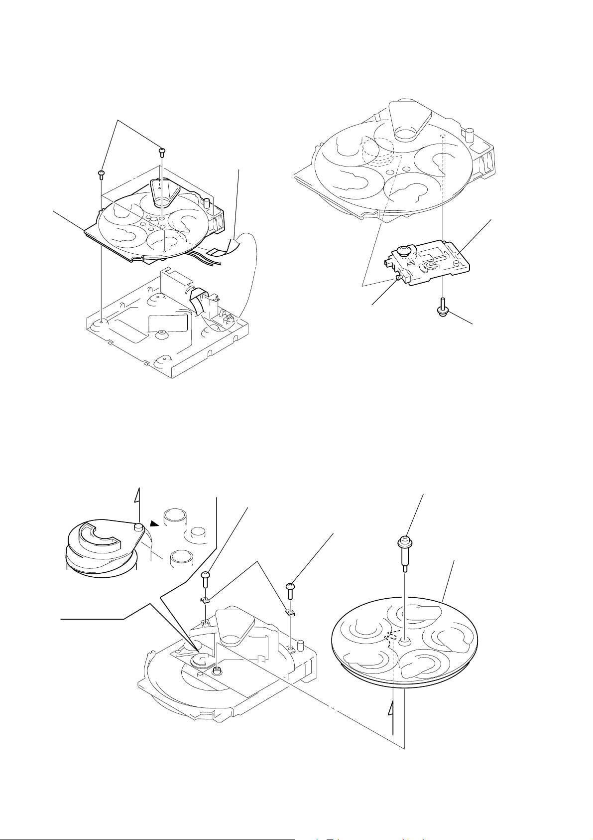
3-6. CD MECHANISM DECK
t
1
Five screws
(BVTP3x8)
2
CD mechanism
deck
3
Flat type wire
3-7. BASE UNIT
2
Boss
3
Base uni
1
Yoke bracket
3-8. DISC T ABLE
Note:
When the disc table is installed, adjust the positions of
roller cam and mark ” as shown in the figure, then set to
the groove of disc table.
A
3
2
Screw (BVTP3x8)
Bracket (BU)
1
Screw (BVTP3x8)
A
4
Stop screw
5
Disc table
— 10 —

SECTION 4
SL703 (AFADJ)
IC751
IC251
SL702 (ADJ)
SL701 (CAL BAR)
TEST MODE
VIDEO CD COLOR-BARS MODE
On this mode, the data of the color-bars signal as a picture signal
and the 1kHz sine wave signal as a sound signal are output by the
mechanism control microcomputer (IC701) for video CD signal
check. When measurement of the voltage and waveform on the
VIDEO board, perform it in this mode.
For refernce, the color-bars signal can be observed at J9001 (VIDEO
OUT) and the sound signal can be observed at J101 (VIDEO (AUDIO) OUT) using an oscilloscope.
1. Connect the lead wire to both ends of the land of SL701 (CAL
BAR) of the VIDEO board.
2. Turn the power on. Press FUNCTION button to select CD.
3. After 2 or 3 seconds later, connect the lead wire.
4. After measuring, remove the lead wire connected.
NOTE:
The 1 kHz sine wave is not outputted when the CD is played once,
but it is not error.
E-F BALANCE MODE
• Refer to SECTION 6 ELECTRICAL ADJUSTMENTS page 15.
1. Connect the lead wire to both ends of the land of SL702 (ADJ)
and SL703 (AFADJ) of the VIDEO board.
2. Turn the power on. Press FUNCTION button to select CD.
3. Short-circuit the lead wire. (At this time, “DISC” on the fluores-
cent indicator tube will blink (test mode). If it is not blinking,
perform from step 1 again.)
4. Press the · button in playback.
5. Every pressing the REPEAT button, the tracking servo and the
sledding servo are turned on or off.
6. When the servo is OFF, the counter on front panel will not be
changed.
7. After measuring, remove the lead wire connected step 1.
[VIDEO BOARD] (SIDE B)
— 11 —
SECTION 5
MECHANICAL ADJUSTMENTS
SECTION 6
ELECTRICAL ADJUSTMENTS
Precaution
1. Clean the following parts with a denatured alcohol-moistened
swab:
record/playback heads pinch rollers
erase head rubber belts
capstan idlers
2. Demagnetize the record/playback head with a head demagnetizer.
3. Do not use a magnetized screwdriver for the adjustments.
4. After the adjustments, apply suitable locking compound to the
parts adjusted.
5. The adjustments should be performed with the rated power supply voltage unless otherwise noted.
T orque Measurement
Torque
FWD
FWD
back tension
REV
REV
back tension
FF/REW
FWD tension
REV tension
Torque meter
CQ-102C
CQ-102C
CQ-102RC
CQ-102RC
CQ-201B
CQ-403A
CQ-403R
Meter reading
36 to 61 g • cm
(0.5 - 0.84 oz • inch)
2 to 6 g • cm
(0.02 - 0.08 oz • inch)
36 to 61 g • cm
(0.5 - 0.84 oz • inch)
2 to 6 g • cm
(0.02 - 0.08 oz • inch)
61 to 143 g • cm
(0.85 - 1.99 oz • inch)
100 g or more
(3.53 oz or more)
100 g or more
(3.53 oz or more)
DECK SECTION 0 dB=0.775V
1. Demagnetize the record/playback head with a head damagnetizer.
2. Do not use a magnetized screwdriver for the adjustments.
3. After the adjustments, apply suitable locking compound to the
parts adjusted.
4. The adjustments should be performed with the rated power supply voltage unless otherwise noted.
5. The adjustments should be performed in the order given in this
service manual. (As a general rule, playback circuit adjustment
should be completed before performing recording circuit adjustment.)
6. The adjustments should be performed for both L-CH and R-CH.
7. Switches and controls should be set as follows unless otherwise
specified.
Tape
P-4-A100
WS-48B
P-4-L300
NOTE:
Set the test mode by following step before performing the adjustment of “DECK SECTION”. All effects for the output signal are
canceled. If the adjustment is not performed in this test mode, you
cannot adjust correctly.
Procedure :
With the power turned ON, press the SPECTRUM ANALYZER
button, ENTER button, and EFFECT button simultaneously.
(The “VOLUME” on the fluorescent display tube will blink while
in the test mode.)
To exit the test mode, press the POWER button.
Signal
10 kHz, –10 dB
3 kHz, 0 dB
315 Hz, 0 dB
Used for
Azimuth Adjustment
Tape Speed Adjustment
Level Adjustment
Record/Playback Head Azimuth Adjustment
(Deck A, Deck B)
Note: Perform this adjustments for both decks.
Procedure:
1. Mode : Playback
test tape
P-4-A100
(10kHz, –10dB)
set
VIDEO(AUDIO)
OUT
level meter
+
–
— 12 —
2. Turn the adjustment screw and check output peaks. If the peaks
e
do not match for L-CH and R-CH, turn the adjustment screw so
that outputs match within 1 dB of peak.
L-CH
peak
output
level
within
1 dB
within 1dB
T ape Speed Adjustment (Deck A)
Note: Set the test mode using the following method and begin tape
speed adjustment.
In the test mode, the tape will move at double speed while
the H SPEED DUB button is pressed.
Procedure :
With the power turned ON, press the SPECTRUM ANALYZER
button, ENTER button, and EFFECT button simultaneously.
(The “VOLUME” on the fluorescent display tube will blink while
in the test mode.)
To exit the test mode, press the POWER button.
R-CH
screw
position
peak
3. Mode: Playback
test tape
P-4-A100
(10kHz, –10dB)
in phase 45
L-CH
peak
VIDEO
(AUDIO)
OUT
L
set
R
Waveform of oscilloscope
°
90
°
good
135
R-CH
peak
°
oscilloscope
180
wrong
°
screw
position
1. Load WS-48B into deck A and a recordable tape into deck B.
2. Press the r REC button, and press the · button of deck B to
set deck B into the recording state.
3. Play deck A.
4. While pressing the H SPEED DUB button, set double speed
play.
5. Adjust RV652 of the AUDIO board so that the reading of the
frequency counter becomes 6000 ± 90 Hz.
6. Release the H SPEED DUB button to set normal speed play.
7. Adjust RV651 of the AUDIO board so that the reading of the
frequency counter becomes 3000 ± 90 Hz.
Adjustment Location: AUDIO board
Sample Value of W ow and flutter
W.RMS (JIS) less than 0.3%
(test tape: WS-48B)
Playback Level Adjustment (Deck A, Deck B)
Procedure:
Mode: Playback
test tape
P-4-L300
(315Hz, 0dB)
set
level meter
4. After the adjustments, apply suitable locking compound to the
parts adjusted.
Adjustment Location: Playback Head (Deck A)
Record/Playback/Erase Head (Deck B)
revers
forward
VIDEO
(AUDIO)
OUT
Deck A is RV311 (L-CH) and RV411 (R-CH), deck B is RV301
(L-CH) and RV401 (R-CH)
so that adjustment within the following adjustment level.
Adjustment level:
CN403 playback level: 301.5 to 338.3 mV (–8.2 to –7.2 dB)
level difference between the channels: within ± 0.5 dB
Adjustment Location: AUDIO board
— 13 —
Record Bias Adjustment (Deck B)
)
Record Level Adjustment (Deck B)
Procedure:
INTRODUCTION
When set to the test mode performed in Tape Speed Adjust-
ment, when the tape is rewound after recording, the “REC memory
mode” which rewinds only the recorded portion and playback is
set.
This “REC memory mode” is convenient for performing this adjustment. During recording, the input signal FUNCTION will automatically switch to VIDEO.
1. Press FUNCTION button to select VIDEO. (This step is not
necessary if the above test mode has already been set.)
2. Load a tape into deck B, and press the r REC button.
3. Mode: Record
VIDEO (AUDIO) IN
1) 315Hz
2) 10kHz
AF OSC
attenuator
} 50 mV (–23.8 dB)
600
Ω
blank tape
CS-123
set
4. Mode: Playback
recorded
position
level meter
Procedure:
INTRODUCTION
When set to the test mode performed in Tape Speed Adjust-
ment, when the tape is rewound after recording, the “REC memory
mode” which rewinds only the recorded portion and playback is
set.
This “REC memory mode” is convenient for performing this
adjustment. During recording, the input signal FUNCTION will
automatically switch to VIDEO.
1. Press FUNCTION button to select VIDEO. (This step is not
necessary if the above test mode has already been set.)
2. Load a tape into deck B, and press the r REC button.
3. Mode: Record
VIDEO (AUDIO) IN
315Hz 50 mV (–23.8 dB)
AF OSC
attenuator
600
Ω
set
blank tape
CS-123
4. Mode: Playback
recorded
position
level meter
set
VIDEO
(AUDIO)
OUT
5. Confirm playback the signal recorded in step 2 become adjustment level as follows.
If these levels do not adjustment level, adjust the RV341 (LCH) and RV441 (R-CH) on the AUDIO board to repeat steps 3
and 4.
Adjustment level: The playback output of 10 kHz level difference
against 315 Hz reference should be ± 1.0 dB.
Adjustment Location: AUDIO board
Adjustment Location
[AUDIO BOARD] (Conductor Side)
RV341 (Lch), RV441 (Rch)
Record Bias
RV301
RV401
RV441 RV341
RV301 (Lch), RV401 (Rch)
Playback Level (Deck B)
RV651 (Normal Speed)
RV652 (High Speed)
Tape Speed
RV311 (Lch), RV441 (Rch)
Playback Level (Deck A)
RV651
RV311
RV411
RV652
set
VIDEO
(AUDIO)
OUT
5. Confirm playback the signal recorded in step 2 become adjustment level as follows.
If these levels do not adjustment level, adjust the RV301 (LCH) and RV351 (R-CH) on the MAIN board to repeat steps 3
and 4.
Adjustment level:
CN403 playback level: 47.2 to 53.0 mV (–24.3 to –23.3 dB)
Adjustment Location: MAIN board
RV301
[MAIN BOARD] (Component Side)
Record Level (L CH
IC401
RV351
Record Level
(R CH)
— 14 —
CD SECTION
NOTE :
1. CD Block is basically designed to operate without adjustment.
Therefore, check each item in order given.
2. Use YEDS-18 disc (3-702-101-01) unless otherwise indicated.
3. Use an oscilloscope with more than 10MΩ impedance.
4. Clean the object lens by an applicator with neutral detergent when
the signal level is low than specified value with the following
checks.
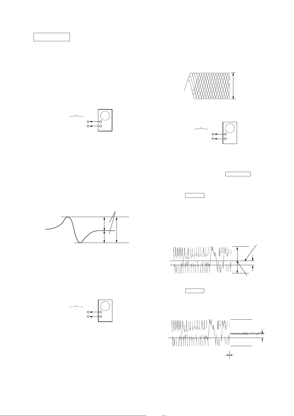
S Curve Check
oscilloscope
BD board
TP (FE)
TP (VC)
Procedure :
1. Connect oscilloscope to test point TP (FE) on BD board.
2. Connect between test point TP (FEI) and TP (VC) by lead wire.
3. Turned Power switch on.
4. Put disc (YEDS-18) in and turned Power switch on again and
actuate the focus search. (actuate the focus search when disc
table is moving in and out.)
5. Check the oscilloscope waveform (S-curve) is symmetrical between A and B.
And confirm peak to peak level within 3±1 Vp-p.
S-curve waveform
+
–
symmetry
A
B
Within 3
±
1 Vp-p
Note : A clear RF signal waveform means that the shape “◊” can
be clearly distinguished at the center of the waveform.
RF signal waveform
VOLT/DIV : 200mV
TIME/DIV : 500ns
level : 1.3 Vp-p
+0.25
–0.20
E-F Balance (T raverse) Check
oscilloscope
BD board
TP (TE)
TP (VC)
+
–
Procedure :
1. Connect oscilloscpe to test point TP (TE) on BD board.
2. Connect the lead wire to both ends of the land of SL702 (ADJ)
and SL703 (AFADJ) of the VIDEO board.
3. Turned Power switch on. Press FUNCTION button to select
CD.
4. Short the lead wire.
5. Put disc (YEDS-18) in to play the number five track.
6. Press the REPEAT button. (The tracking servo and the sledding servo are turned OFF.)
7. Check the level B of the oscilliscope's waveform and the A (DC
voltage) of the center of the Traverse waveform.
Confirm the following :
A/B x 100 = less than ± 22%
T raverse waveform
Center of the waveform
6. After check, remove the lead wire connected in step 2.
Note : • Try to measure several times to make sure than the ratio
of A : B or B : A is more than 10 : 7.
• Take sweep time as long as possible and light up the brightness to obtain best waveform.
RF Level Check
oscilloscope
BD board
TP (RF)
TP (VC)
+
–
Procedure :
1. Connect oscilloscope to test point TP (RF) on BD board.
2. Turned Power switch on.
3. Put disc (YEDS-18) in to play the number five track.
4. Confirm that oscilloscope waveform is clear and check RF signal level is correct or not.
B
0V
level : 1.3
A (DC voltage)
±
0.6 Vp-p
8. Press the REPEAT button. (The tracking servo and sledding
servo are turned ON.) Confirm the C (DC voltage) is almost
equal to the A (DC voltage) is step 7.
T raverse waveform
C (DC
0V
Tracking servo
Sled servo
OFF
Tracking servo
Sled servo
ON
voltage)
9. Remove the lead wire connected step 1.
— 15 —
RF PLL Free-run Frequency Check
Procedure :
1. Connect frequency counter to TP (PLCK) with lead wire.
VIDEO SECTION
Frequency adjustment
BD board
TP (PLCK)
frequency counter
+
–
2. Turned Power switch on.
3. Put the disc (YEDS-18) in to play the number five track.
Confirm that reading on frequency counter is 4.3218MHz.
1. Connect the frequency counter to check point of the VIDEO
board.
frequency counter
VIDEO board
TP410 (DCLK)
+
–
2. Adjust CT401 of the VIDEO board so that the frequency counter
read 13.5MHz ± 40Hz at STOP condition.
Adjustment Location :
[ BD BOARD ] — SIDE A — [ VIDEO BOARD ] — SIDE B —
1
10 11
(PLCK)
IC103
IC101
20
(VC)
(RF)
(TE)
(FE)
(FEI)
SL703 (AFADJ)
SL702 (ADJ)
IC751
SL701 (CAL BAR)
CT401
Frequency
IC251
TP410 (DCLK)
— 16 —
7-1. CIRCUIT BOARDS LOCA TION
d
d
SECTION 7
DIAGRAMS
TRANS board
VIDEO POWER board
HP/MIC board
TC-A SW board
CD-LED board
CD-A SW board
DOOR SW board
PANEL board
TC-B SW board
CD-B2 SW board
FM/AM TUNER PACK
SURROUND boar
MAIN board
KEY CON board
VIDEO OUT board
VIDEO board
POWER board
CD-B1 SW board
Note: pA is including in AUDIO board.
AUDIO board
(including
TABLE SENSOR board
p
A)
p
A
MOTOR board
LEAF SWITCH boar
BD board
CD MOTOR board
LED board
— 17 —
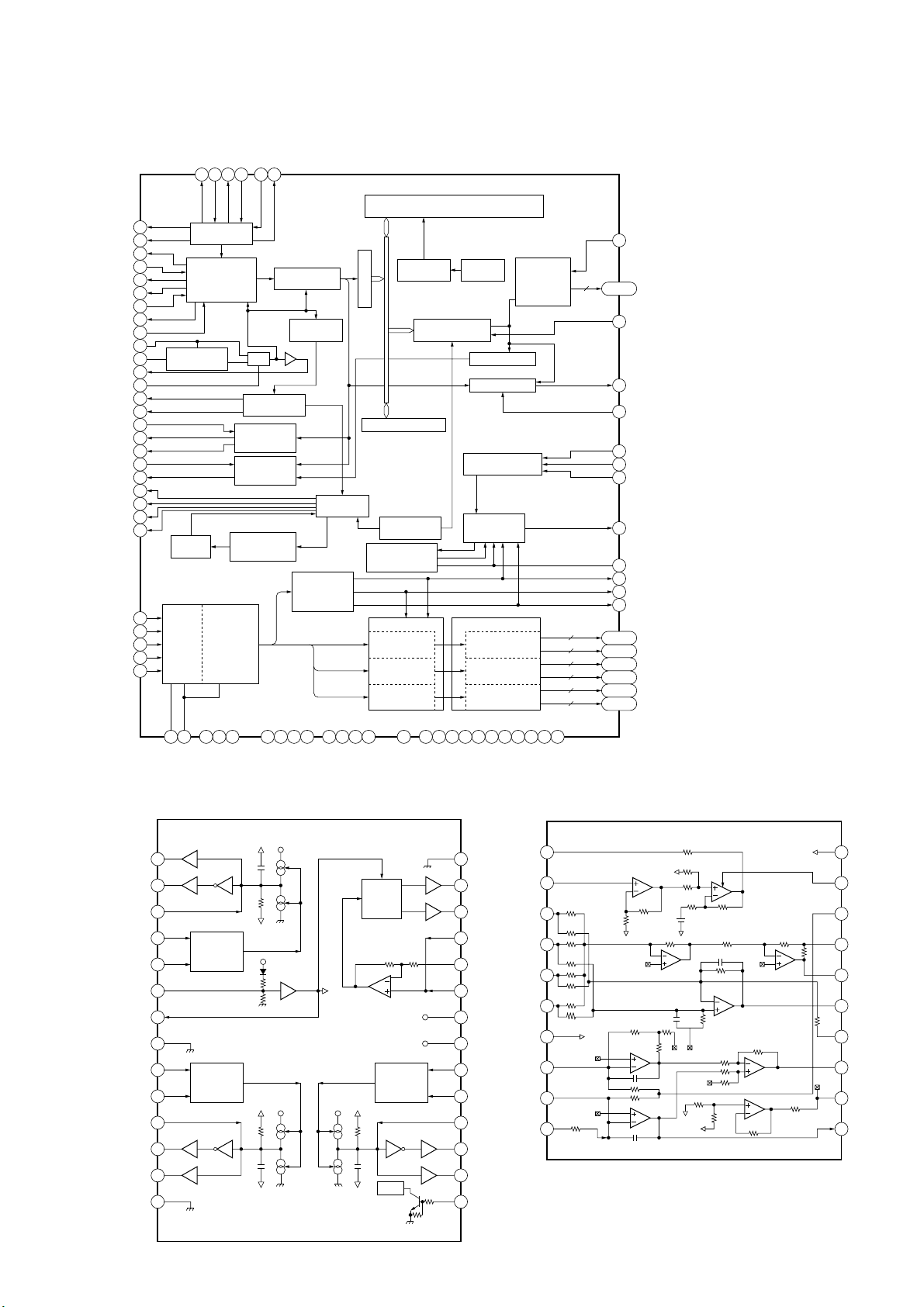
7-2. BLOCK DIAGRAMS
— KEY CON SECTION —
HCD-V8800
J761
MIC 1
J762
MIC 2
MIC AMP
IC760 (1/2)
31
RV760
MIC LEVEL
1
LPF1
ECHO AMP
IC760 (2/2)
67
ECHO
IC761
2
SWITCH
IC1403
5
3
9
LPF2
4
8
RV761
ECHO LEVEL
L IN
Q1401
91011
K CON
KEY CONTROL
IC1401
LPF1
IN
22
MIX
OUT
15
A
Rch
DATA
CLOCK
STORBE
9
78
LATCH
CLK
DATA
L OUT
09
• R CH : Same as Lch
• Signal path
: FM
: MIC
MAIN
SECTION
(Page 25)
— 18 —
HCD-V8800
— CD SECTION —
OPTICAL PICK-UP
BLOCK (KSS-213D/Q-NP)
LASER
DIODE
PD
DETECTOR
E
AC
BD
F
LD
TRACKING
COIL
FOCUS
COIL
LD
POWER
1
4
M102
SLED
MOTOR
M101
SPINDLE
MOTOR
LD
DRIVE
Q101
VC
RF AMP
IC103
APC LD
2
AMP
RF FQ
AMP
19
RF
INTEGRATOR
16
15
13
1110
VC
12
INTE-
GRATOR
4
5
19
20
10
9
23
24
15MUTE
1
3
4
5
6
8
9
T+
1
T–
F+
16
F–
17
13
M
12
27
M
26
09
RF
SUMMING
AMP
FOCUS
ERROR
AMP
TRACKING
ERROR
AMP
VC
BUFFER
FOCUS/TRACKING COIL DRIVE
SPINDLE/SLED MOTOR DRIVE
IC102
2
DIGITAL SERVO
DIGITAL SIGNAL PROCESSOR
IC101
ASY0
39
RF AC
36
ASY1
38
RF DC
26
TE
27
SE
28
FE
29
TFDR
4
TRDR
6
FFDR
8
FRDR
10
SRDR
2
SFDR
100
MDP
96
ASYMMETRY
CORRECTION
A/D
CONVERTER
MIRR
DFCT
FOK
DETECTOR
MIX
FOK
DFCT
MIRR
SERVO DSP
FOCUS
SERVO
TRACKING
SERVO
SLED
SERVO
PWM
GENERATOR
TRACKING
PWM
GENERATOR
FOCUS
PWM
GENERATOR
SLED
PWM
GENERATOR
DIGITAL
PLL
CLOCK
GENERATOR
EFM
DEMODULATOR
62
XTAL
SYNC
PROTECTOR
TIMING
GENERATOR 1
CLV SERVO
PROCESSOR
1B TIMS
OVERSAMPLING
FILTER
NOISE
SHAPER
REGISTER
DATA BUS
ERROR
CORRECTOR
TIMING
GENERATOR 2
PRIORITY
EMCODER
ADDRESS
GENERATOR
32K
RAM
D/A
DATA
PROCESSOR
MUTE
79 54
M201
TABLE
MOTOR
GFS
M
DIGITAL
OUT
PEAK
DETECTOR
SERIAL/PARALLEL
PROCESSOR
INTERFACE
S STOP
99
+5V
SWITCH
MOTOR DRIVER
OUT1
7
3
OUR2
SERVO
S901
LIMIT
IC201
SUBCODE
P-W
PROCESSOR
SUBCODE
Q
PROCESSOR
INTERFACE
SEQUENCER
IN1
9
1
IN2
CPU
SERVO
AUTO
S201
UP SW
DISC
TABLE
SENSOR
IC202
MD2
DOUT
EXCK
SBSO
SUBQ
SQCK
SCLK
DATA
LRCK
BCLK
SCOR
WFCK
DATA
XLT
CLK
SENS
C2PO
FOK
DFCT
MIRR
XRST
+5V
70
71
76
75
77
78
83
46
45
47
74
73
86
87
88
80
56
93
92
91
81
LDON
384FS
SUBQ
SQCK
SCLK
ADATA
LRCK
BCK
SCOR
DATA
XLT
CLK
SENS
C2PO
XRST
AMUTE
UP SW
T.SENS
B
VIDEO
SECTION
(Page 21)
C
MAIN
SECTION
(Page 25)
TBL.L
TBL.R
— 19 —
• R CH: Same as L ch
• SIGNAL PATH
: CD
: VIDEO
— 20 —
HCD-V8800
— VIDEO SECTION —
BCK
ADATA
IC501
(2/2)
LRCK
C2PO
384FS
ADATA
LRCK
BCLK
28.63636MHz
45.1584MHz
DATA
CLK
AMUTE
384FS
416
384FS
DATA
CLK
AMUTE
SQCK
SUBQ
SCLK
XLT
LDON
SCOR
SENS
XRST
X202
X201
B
CD
SECTION
(Page 20)
B
CD
SECTION
(Page 20)
09
IC501 (1/2)
9
8
7
6
5
106
107
73
78
74
11
10
77
76
75
71
62
48
BUFFER
XTL0O
2
XTL01
3
XTL2O
XTL2I
DATA
CLK
AMUTE
SQCK
SUBQ
SCLK
XLT
LDON
SCOR
SENS
RESET
38–43 46–55•
•
•11–13 15–19
D0
112
111
110
109
103
100
101
102
D-RAM INTERFACE
17–21 23 24 32 33••••
•
A0
I/O8
2–10 21 23–25
21–29 • 31–3513 – 20
A0
D7
11
12
13
14
15
2–5 7–10 35–38 40–43
•
DQ1
I/O1
18–21 24–28•
DQ16
D-RAM
IC251
S-RAM
IC751
••
CD-ROM
DECODER
MPEG
AUDIO
DECODER
A0
A12
A12
MPEG DECODER
IC201
VIDEO
POSTPROCESSOR
SYNC GENERATOR
A0
A3
XTCS
AS
DECODER
7–13 16
LCAS
UCAS
IC772
WE
6
54
3
12
40
A17
IC701
MPEG
VIDEO
EACH CIRCUIT BLOCK
HOST INTERFACE
5 6•• •119 120
•
D0
D7
IC771
MPEG
SYSTEM
DECODER
34
3735
301516 31
W
A8
RAS
CE1
OE
55
RD
272022
8
10 9
11
12
13
41 54 56 43 70 7 8
A18
MECHA CONTROL
&
XHCS
XWR
WR
XHDT
WAIT
117115116114
XHIRQ
XHIRQ
EXTAL
Y
C
118
VDAC-XLAT
XTAL
5251
71
74
•
76
80
63
70
97
95
92
93
94
89
56
57
58
59
XRST
GENERATOR
DF-XLAT
X701
10MHz
XSGRST
HSYNC
VSYNC
FID
DCLK
XOSDEN
OSD B
OSD G
OSD R
CLOCK
IC272
CMD0
CMD1
CMD2
CMD3
SACK
QINT
MREQ
NPIN
Y0-Y7
C0-C7
1
2
3
4
5
6
72
64
OSD B
OSD G
OSD R
XOSDEN
VSYNC
HSYNC
DCLK
SYSTEM SELECT
1
4
Y
•
6
9
11
C
18
18
17
16
15
19
20
CK 1/2 Q
1 5
S9001
RGB-YUV
CONV.
TIMING
GEN.
98 10097
HSYNC
OUTPUT
CONT.
SYNC
CONT.
PAL
AUTO
NTSC
NOISE REDUCTION
REDUSER
MEMORY
DCLKI
VSYNC
DCLK
VIDEO
RAM
DATA
SEL.
34
CMD0
35
CMD1
CMD2
36
37
CMD3
44
SACK
18
QINT
MREQ
43
IC301
NOISE
CONT.
OSD
IC271
6.75MHz
CD-XRST
YUV-RGB
CONV.
DRAM
IF
DATA INPUT
SHIFT
RESISTOR
DISPLAY
POSITION
CONT.
OSC
8
IIC INTERFACE
IC901
10BIT VIDEO D/A CONVERTER
IC401
60
67
51
58
29
30
31
4
3
2
1
NR-XCS
MCLK
MDATA
RESET
MDATA
OS-XLAT
MCLK
1
4
•
6
9
11
18
CT401
13.5MHZ
DEMPX, LEVEL
TRANSLATOR
&
INTERPOLTATOR
CLOCK GENARATOR
IC402
56
4
3
X401
27MHz
VIDEO AMP
IC451
V
HSYNC
Y, C/Y, U, V
SELECTOR
&
INTER-
POLATOR
CLOSED
CAPTION
ENCODER
SIO & I2O-BUS
CONT.
49 504859 60625557 51
VDAC-XLAT
CLK
DATA
Y
C
LPF
LPF
DELAY
56
1/2
XRST
DCLK
MODULATOR
SYNC
SLOPE
GEN.
SYNC GEN.
TIMING CONT.
XVRST
&
FID
SUB
CARRIER
GEN.
VSYNC
24
29325
5 7
3
Y/C AMP
IC452
7
1
J9001
VIDEO OUT
4
3
J9002
S VIDEO OUT
• R CH: Same as L ch
• SIGNAL PATH
: VIDEO
: Y
: CHROMA
: CD
DIGITAL FILTER & D/A CONVERTER
384FS
BUFFER
IC181
ADATA
13
LRCK
4
BCLK
1
DATA
CLK
DF-XLAT
68494847
MCLK
MDATA
NR-XCS
OS-XLAT
15
RESET
55
IIC-DATA
56
X2
IIC-CLK
X1
111052
X901
5MHz
AMUTE
XRST
11
6
3
6
11
12
10
3
4
5
2
TIMING
CIRCUIT
INPUT PLM
MODE
IC101
D/A
CONV.
CLOCK
GENERATOR
MUTE
CIRCUIT
INT
1
21
22
27
25
16
18
L CH
XRST
IIC-DATA
IIC-CLK
ACTIVE LPF
2
3
X101
33.8688MHz
IC102
16 7
R CH
D
MAIN
SECTION
(Page 25)
— 21 —
— 22 —
HCD-V8800
— DECK SECTION —
HP101
PB HEAD
(DECK A)
REC/PB HEAD
(DECK B)
HRPE101
ERASE HEAD
PB A/B
PB L
LM ON/OFF
NORM/HIGH
NR ON/OFF
REC/PB/PASS
REC L
BIAS ON/OFF
RM ON/OFF
RELAY REC/PB
CAP M ON/OFF
CAP M H / L
A SHUT
E
MAIN
SECTION
(Page 25)
13
DOLBY NR
RECOUT
NORM
24 25
S1008
B CrO
15
B 120/70
BIAS SW
CROM
2
PAS
DOL
DOLBY
TYPE B
M1
CAPSTAN
MOTOR
CN403
3
R CH
1
PB OUT
8
LM ON/
20
OFF
NORM/
14
HIGH
NR ON/
18
OFF
19
PB
RIN
6
BIAS ON/OFF
RM ON/OFF
M
CAP M SWITCH
Q405, 407
SPEED
CONTROL
RV651
NORMAL
SPEED
Q651
16
17
RV652
HIGH
SPEED
SWITCH
Q406
REEL
DETECT
Q1001
S1004
A CrO2
RV311
4
PLAYBACK
LEVEL
DECK A
RV301
PLAYBACK
LEVEL
DECK B
RV341
REC
BIAS
REC BIAS
BIAS OSC
T621, Q621, 622
IC611
L
R
L
R
X
R CH
R CH
3
P
ERASE BIAS
IC601
1
IC602
R
REC/PB
12
PB-A/B
A IN
2
B IN
4
REC LEVEL
+7.5V
EQIN
Q623, 901
10
EQOUT
11
A 120/70
70
120
DECK PROCESS
IC401
RV301
10
REEL
DETECT
Q1002
S1001 (A PLAY)
• R CH : Same as L ch
• SIGNAL PATH
+5V
S1002 (B PLAY)
: PB (DECK A)
: PB (DECK B)
: REC (DECK B)
09
2
OUT1
OUT2
TRIGGER
MOTOR
DRIVE
IC402
M2
TRIGGER
MOTOR
M
10
S1003
(A HALF)
S1005
(REC A)
S1006
(B HALF)
S1009
(REC B)
VZ
IN2
IN1
+5V
4
6
5
SWITCH
Q408, 409
B SHUT
A PLAY
B PLAY
A HALF
BHALF
TRIG H / L
B TRIG
A TRIG
— 23 —
— 24 —
HCD-V8800
— MAIN SECTION —
KEY CON
SECTION
A
(Page 18)
E
DECK
SECTION
(Page 24)
FM/AM
TUNER PACK
ENCAPSLATED
COMPONENT
C
CD
SECTION
(Page 20)
D
VIDEO
SECTION
(Page 22)
09
J101
PHONO
IN
L
IN L
VIDEO
(AUDIO)
OUT L
LATCH
K CON
L OUT
J101
REC L
RELAY REC/PB
A SHUT
B SHUT
B HALF
A HALF
A PLAY
B PLAY
PB A / B
NORM/HIGH
BIAS ON/OFF
RM ON/OFF
NR ON/OFF
REC/PB PASS
LM ON/OFF
CAP M H/L
A TRG
B TRG
TRIG H/L
CAP M ON/OFF
COM DIN
COM DATA
STEREO
TUNED
MUTE
TBL. L
TBL. R
UP SW
T. SENS
IIC-DATA
IIC-CLK
L IN
DATA
CLK
PB L
ST L
ST CE
L CH
XRST
3
4
5
6
31
PHONO EQ AMP
IC101
MUTE
Q121
V
TC
ST
CD
INPUT SELECT
IC102
1
2
4
5
MUTE
CONTROL
Q123,124
A
B
INH
D+5V
D201
(DISC No.)
3
10
9
6
1
2
3
4
5
6
Q201
— 25 —
INPUT SELECT
3
5
96
RELAY
26
A SHUT
27
B SHUT
28
B HALF
97
A HALF
94
A PLAY SW
95
B PLAY SW
87
PB A/B
88
EQ H//N
89
BIAS
90
REC MUTE
91
NR ON/OFF
R/P PASS
92
93
TC MUTE
82
CAP H/N
83
A TRG
84
B TRG
85
TRG LOW
86
CAP M ON/OFF
41
VOL LAT
42
PL LAT
44
COM DOUT
45
COM CLK
66
ST DIN
70
STEREO
TUNED
69
68
ST CE
72
ST MUTE
67
ST DOUT
4
K CON LAT
5
K CON ON
60
TBL L
61
TBL R
UP SW
77
76
T SENS
XRST
57
62
TRAY LED
IC103
4
9
10
11
DOLBY PRO LOGIC
9
L-IN
3
41
DATA
4
42
CLK
2
40
EN
69
71
28
29
30
54
INPUT CHANGE
MASTER CONTROL
IC601
IC701
C-OUT
S-OUT
L-OUT
INTERFACE
32 33
4
CENTER
34
REAR
35
37
FRONT
65 64
MICON
34
3
LATCH
3
427 LAT SW F CON
VOLUME
3
IN
14
IN
8
CLK
9
DATA
10
LED
CONTROL
Q601
REMOTE
CONTROL
RECEIVER
IC602
S711
ROTARY
ENCODER
KEY
MATRIX
S681
6
OPEN
IC604
MUTE
Q254
MUTE
SWITCH
Q120
PANEL LED
OUT
OUTLATCH
Q602
MUTE
15
Q601
Q602,603
MUTE
2
• R CH: Same as L ch
• SIGNAL PATH
: FM
: CD
: PB
: REC
: VIDEO
REAR
CENTER
FRONT
DBFB
POWER ON/OFF
R RELAY
D+5V
CD POWER
STK MUTE
REAR
CENTER
F
POWER
SECTION
(Page 27)
DELAY
IC602
S-IN
L-IN
DATA
CLK
EN
POWER
DBFB H/L
TA MUTE
R RELAY
IIC DATA
IIC CLK
RESET
AC CUT
XT1
XT2
CD POWER
STK MUTE
S-OUT
FRONT
X1
X2
L-MIX
OUT
XTAL
XTAL
REC 2A
62
98
2
1
7
55
56
15
20
11
10
14
13
46
100
13
16
23
24
EQ
61
D951
FRONT
RESET
SWITCH
Q951
RESET
IC951
+5V
X701
5MHz
X702
32.768KHz
X601
8MHz
X601
8MHz
MUTE
SWITCH
Q912
45 44 43 42
EQUALIZER / VOLUME
IC201
DATA
28
CLOCK
27
14
RESET
12
XOUT
13
XIN
SEG1–35
67 – 100 • 1
FLUORESCENT INDICATOR TUBE
+ +
S.WOOFER
SWITCH
DISPLAY CONTROL
IC601
GR1–16
51 – 66
FL601
10
8
3
3
4
2
2
4
99
REAR
CENTER
6
5
39
MODE
Q206
LED18
LED SELECT
SIRCS
SPEANA 1
SPEANA 2
SPEANA 3
SPEANA 4
DOOR SW
VF
AMP
IC861
BB22
40
DBFB
SWITCH
Q201
LED1
L+R
JOG A
JOG B
KEY 5
KEY 1
VOL A
VOL B
IC603
3
5
BB12
41
1
AMP
7
7
FRONT
38
DBFB
SWITCH
Q202
3
10
•
15
•
16
•
18
LED
SWITCH
23
•
25
•
47
29
39
42
43
44
45
46
26
41
37
33
38
24
40
D/A
S701
VOLUME
ROTARY
ENCODER
4
3
1
= AMS +
— 26 —
HCD-V8800
— POWER SECTION —
F
MAIN
SECTION
(Page 26)
09
REAR
CENTER
FRONT
DBFB
STK MUTE
R RELAY
CD POWER
POWER ON/OFF
FRONT
POWER AMP
IC201
1 10
6
D5V
SWITCHED
AU/D5V SW
REAR
CENTER
Rch
+5V REG
THERMAL
DET
Q670,671
THP670
OVER LOAD
DET
Q201
Q906
Q907
OVER LOAD
MUTE
SWITCH
Q331
1
DET
Q601,651
POWER AMP
IC601
1318
6
Rch
+5V
D905
D7V
A+7.5V
A–7.5V
+12V
ST 10V
PRO-LOG 10V
10
Q323
Rch
+7.5
1
–7.5 EN
10
2
1
+5V REG
IC902
3 1
+7V REG
IC903
3 1
+7V, –7V REG
IC901
4
+12V REG
IC904
3 1
3 1
+10V REG
IC905
Q901
RY401
RY402
6
PROTECTOR
PROTECT
SWITCH
VCC
2
9
VEE
POWER B+
POWER B–
–1
–2
IC301
7
Q301
UNREG
–12V
SURR B+
SURR B–
–1
A+5V
(SW)
4
RELAY
DRIVE
Q403
+5V SW
Q9003
RECT
D901
RECT
D101
RECT
D102
RELAY
DRIVE
Q404
RELAY
CONTROL
Q402
Q9004
+5V REG
IC9002
3 1
VFDP
Rch
HP / SP
SWITCHING
Q401,405
RECT
D302,303
VF REG
Q941
CENTER
FAN MOTOR
DRIVER
Q961, 962
D+3.3V
RECT
D104,105
REAR
FRONT
Rch
VF
VF
SURROUND
UNREG
–12V
SPEAKER
+3.3V REG
IC801
2 1
T501
POWER
TRANSFORMER
TM402
SPEAKER
M
TM401
FRONT
J760
PHONES
REAR
CENTER
M901
FAN
MOTOR
D+5V
(SW)
E,SP,IA,CH
VOLTAGE
SELECTOR
S501
D+5V
(UNSW)
+5V SW
Q9001
AC
IN
+5V REG
IC9001
3 1
Q9002
• R CH : Same as L ch
• SIGNAL PATH
: FM
• Abbreviation
SP : Singapore model.
IA : Indonesian model.
CH : Chinese model.
— 27 — — 28 —
7-19. IC BLOCK DIAGRAMS
• BD section
IC101 CXD2545Q
FSTO
XTAI
XTAO
XTSL
VCKI
67 62 63 64 20 19
68
C4M
69C16M 43 PSSL
18PDO
13VCO1
12VCO0
33PCO
32FILI
31FILO
34CLTV
36RFAC
38ASYI
39ASYO
42ASYE
73WFCK
74SCOR
76EXCK
75SBSO
72EMPH
78SQCK
77SQSO
95MON
94FSW
96MDP
97MDS
26RFDC
27TE
28SE
29FE
3025VC
GENERATOR
(
DOUBLE SPEED
ASYMMETRY
CORRECTION
NOISE
SHAPER
SWITCH
&
BUFFER
CLOCK
DIGITAL
PLL
VARI-PITCH
A/D
CONVERTER
VPCO
DEMODULATOR
)
MUX
TIMING
GENERATOR 1
SUBCODE
P-W
PROCESSOR
SUBCODE
Q
PROCESSOR
18-TIMES
OVERSAMPLING
FILTER
EFM
SYNC
PROTECTOR
CLV
PROCESSOR
MIRR
DFCT
FOK DETECTOR
32K RAM
ADDRESS
GENERATOR
RESISTER
DATA PROCESSOR
ERROR CORRECTOR
TIMING
GENERATOR 2
SERVO
MICRO PROGRAM
INTERFACE
SERVO DSP PWM GENERATOR
SLED SERVO
TRACKING
SERVO
FOCUS SERVO
PRIORITY
ENCODER
D/A
PEAK DETECTOR
CPU INTERFACE
SEQUENCER
TRACKING PWM
DIGITAL OUT
GENERATOR
GENERATOR
FOCUS PWM
GENERATOR
SERVO
AUTO
SLED PWM
SERIAL
PARALLEL
PROCESSOR
2
2
2
2
2
2
16
DA01-1661-46
79 MUTE
71 D OUT
70 MD2
86 DATA
88 CLOK
87 XLAT
80 SENS
89 COUT
91 MIRR
92 DFCT
93 FOK
SFON, SFDR3, 100
SRON, SRDR1, 2
TFDR, TFON4, 7
TRON, TRDR5, 6
FFDR, FFON8, 11
FRON, FRDR9, 10
24
14
RFC
ADIO
IC102 BA6392FP
BUFF
1CH1 OUT F
BUFF
2CH1 OUT R
3CAPA IN 1
R
4CH1 R IN
INTERFACE
F
5CH1 F IN
6VREF IN
7VREF OUT
8GND
FF
9CH2 F IN
INTERFACE INTERFACE
RR
10CH2 R IN
11CAPA IN 2
BUFF BUFF
12CH2 OUT R
BUFF
13CH2 OUT F
14GND
16
TES2
TEST17TES3
21
AVDD40AVDD
23
BUFF
AVSS35AVSS
F
R
RRFF
41
ADD90ADD
15
DVSS65DVSS
LEVEL
SHIFT
MUTE
81
22
37
44
45
66
82
83
84
85
98
99
FSTI
BIAS
XRST
IGEN
WDCK
LRCK
DIRC
SCLK
DFSW
ATSK
LOCK
SSTP
IC103 CXA1821M
28 GND
BUFF
27 CH4 OUT F
26 CH4 OUT R
BUFF
25 VB IN
24 VS IN
23 VB IN
22 VCC
21 VCC
20 CH3 F IN
19 CH3 R IN
18 CAPA IN 3
17 CH3 OUT R
BUFF
16 CH3 OUT F
15 MUTE
1
LD VCCVCC
PD LD ON
2
A LC/PD
3
B RFE
4
C RFO
5
D FE
6
VEE FE BIAS
F TE
E VC
EI EO
VEE
7
VC
8
9
VC
10
VCC
VREF
VEE
VC
RF SUMMING AMP
VC
APC LD AMP
VEE
TRACKING ERROR AMP
VC
VC
VCC
VEE
RF EQ AMP
VC
FOCUS ERROR AMP
VC BUFFER
20
19
18
17
16
15
14
13
VC
12
11
— 73 —
 Loading...