

Sony HCDRG-551 Service manual
HCD-GX750/RG551/RX550
SERVICE MANUAL
Ver 1.0 2004. 04
• HCD-GX750/RG551/RX550 is the
tuner, deck, CD and amplifier
section in MHC-GX750/RG551S/
RX550.
(Photo: HCD-GX750)
CD
Section
Tape Deck Model Name Using Similar Machanism NEW
Section T ape Transport Mechanism Type CWM43FF-05
US Model
HCD-GX750/RX550
Canadian Model
HCD-GX750
E Model
HCD-RG551
Model Name Using Similar Mechanism NEW
CD Mechanism Type CDM74-F1BD81
Optical Pick-up Name KSM-215DCP/C2NP
AUDIO POWER SPECIFICATIONS
(HCD-GX750 USA model only)
POWER OUTPUT AND TOTAL HARMONIC
DISTORTION:
With 6 ohm loads, both channels driven, from
120 – 10,000 Hz; rated 160 watts per channel
minimum RMS power, with no more than 10 %
total harmonic distortion from 250 milliwatts to
rated output.
Amplifier section
North American models:
HCD-GX750/RX550:
Front speaker
Continuous RMS power output (reference):
160 + 160 watts (6 ohms at
1 kHz, 10% THD)
Total harmonic distortion less than 0.07% (6 ohms at
1 kHz, 80 W)
Sub woofer
Continuous RMS power output (reference):
180 watts (6 ohms at
50 Hz, 10% THD)
Total harmonic distortion less than 0.07% (6 ohms at
50 Hz, 90 W)
SPECIFICATIONS
Other models:
HCD-RG551:
The following measured at AC 120, 127, 220, 240 V,
50/60 Hz
Front speaker
DIN power output (rated): 100 + 100 watts
(6 ohms at 1 kHz, DIN)
Continuous RMS power output (reference):
120 + 120 watts (6 ohms at
1 kHz, 10% THD)
Sub woofer
DIN power output (rated): 100 watts (6 ohms at
50 Hz, DIN)
Continuous RMS power output (reference):
120 watts (6 ohms at
50 Hz, 10% THD)
Inputs
GAME INPUT AUDIO L/R (phono jacks):
voltage 250 mV,
impedance 47 kilohms
GAME INPUT VIDEO (phono jack):
1 Vp-p, 75 ohms
Outputs
PHONES (stereo mini jack):
accepts headphones of
8 ohms or more
– Continued on next page –
9-877-777-01
2004D04-1
© 2004. 04
MINI HI-FI COMPONENT SYSTEM
Sony Corporation
Home Audio Company
Published by Sony Engineering Corporation
1

HCD-GX750/RG551/RX550
VIDEO OUT (phono jack):max. output level
1 Vp-p, unbalanced, Sync
negative, load impedance
75 ohms
SPEAKER: accepts impedance of 6 to
16 ohms
SUB WOOFER OUT: accepts impedance of 6 to
16 ohms
CD player section
System Compact disc and digital
audio system
Laser Semiconductor laser
(λ=770 – 810 nm)
Emission duration:
continuous
Frequency response 2 Hz – 20 kHz (±0.5 dB)
Signal-to-noise ratio More than 90 dB
Dynamic range More than 90 dB
Tape deck section
Recording system 4-track 2-channel, stereo
Frequency response 50 – 13,000 Hz (±3 dB),
using Sony TYPE I
cassettes
Tuner section
FM stereo, FM/AM superheterodyne tuner
FM tuner section
Tuning range
North American model: 87.5 – 108.0 MHz (100 kHz step)
Other models: 87.5 – 108.0 MHz (50 kHz step)
Antenna FM lead antenna
Antenna terminals 75 ohms unbalanced
Intermediate frequency 10.7 MHz
General
Power requirements
North American models: 120 V AC, 60 Hz
Argentine model: 220 V AC, 50/60 Hz
Mexican model: 127 V AC, 60 Hz
Other models: 120 V, 220 V or 230 –
240 V AC, 50/60 Hz
Adjustable with voltage
selector
Power consumption
USA model:
HCD-GX750/RX550: 230 watts
Canadian models:
HCD-GX750: 280 VA
Other models:
HCD-RG551: 275 watts
Dimensions (w/h/d) incl. projecting parts and controls
Amplifier/Tuner/Tape/CD section:
Approx. 280 × 327 × 425 mm
Mass
North American models:
HCD-GX750/RX550: Approx. 10.5 kg
Other models:
HCD-RG551: Approx. 10.5 kg
Design and specifications are subject to change without
notice.
AM tuner section
Tuning range
Pan-American models: 530 – 1,710 kHz (with the tuning
Other models: 530 – 1,710 kHz (with the tuning
Antenna AM loop antenna
Antenna terminals External antenna terminal
Intermediate frequency 450 kHz
interval set at 10 kHz)
531 – 1,710 kHz (with the tuning
interval set at 9 kHz)
interval set at 10 kHz)
531 – 1,602 kHz (with the tuning
interval set at 9 kHz)
2
HCD-GX750/RG551/RX550
SAFETY CHECK-OUT
After correcting the original service problem, perform the following
safety check before releasing the set to the customer:
Check the antenna terminals, metal trim, “metallized” knobs, screws,
and all other exposed metal parts for A C leakage. Check leakage as
described below.
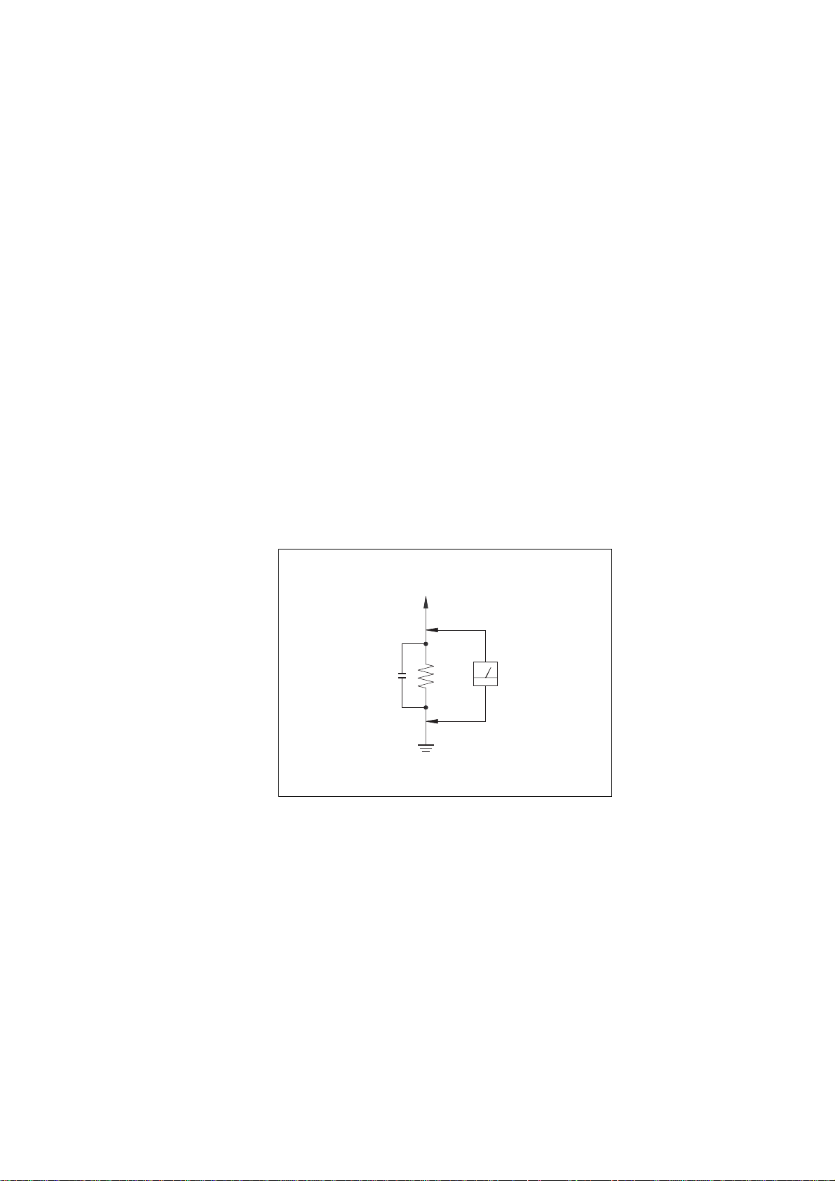
LEAKAGE TEST
The AC leakage from any exposed metal part to earth ground and
from all exposed metal parts to any exposed metal part having a
return to chassis, must not exceed 0.5 mA (500 microamperes).
Leakage current can be measured by any one of three methods.
1. A commercial leakage tester, such as the Simpson 229 or RCA
WT-540A. Follow the manufacturers’ instructions to use these
instruments.
2. A battery-operated AC milliammeter. The Data Precision 245
digital multimeter is suitable for this job.
3. Measuring the voltage drop across a resistor by means of a VOM
or battery-operated AC voltmeter . The “limit” indication is 0.75
V, so analog meters must have an accurate low-voltage scale. The
Simpson 250 and Sanwa SH-63Trd are examples of a passive
VOM that is suitable. Nearly all battery operated digital
multimeters that have a 2V AC range are suitable. (See Fig. A)
To Exposed Metal
Parts on Set
AC
0.15
µ
F
Fig. A. Using an A C v oltmeter to check A C leakage.
Ω
1.5 k
Earth Ground
Voltmeter
(0.75 V)
SAFETY-RELATED COMPONENT WARNING!!
COMPONENTS IDENTIFIED BY MARK 0 OR DOTTED LINE
WITH MARK 0 ON THE SCHEMATIC DIAGRAMS AND IN
THE PARTS LIST ARE CRITICAL TO SAFE OPERATION.
REPLACE THESE COMPONENTS WITH SONY P ARTS WHOSE
PART NUMBERS APPEAR AS SHOWN IN THIS MANUAL OR
IN SUPPLEMENTS PUBLISHED BY SONY.
ATTENTION AU COMPOSANT AYANT RAPPORT
À LA SÉCURITÉ!!
LES COMPOSANTS IDENTIFIÉS PAR UNE MARQUE 0 SUR LES
DIAGRAMMES SCHÉMATIQUES ET LA LISTE DES PIÈCES
SONT CRITIQUES POUR LA SÉCURITÉ DE FONCTIONNEMENT.
NE REMPLACER CES COMPOSANTS QUE PAR DES PIÈCES
SONY DONT LES NUMÉROS SONT DONNÉS DANS CE MANUEL
OU DANS LES SUPPLÉMENTS PUBLIÉS PAR SONY.
3
HCD-GX750/RG551/RX550
The release method of a CD disc tray LOCK function
There is a disc lock function for the disc theft prevention for a
demonstration at a shop front in this machine.
Procedue:
1. Press the ?/1 button to turn the set on.
2. Press two buttons of x and Z (EJECT) simultaneously for
five seconds.
3. The message “LOCKED” is displayed and the tray is locked.
(Even if exiting from this mode, the tray is still locked.)
4. Press two buttons of x and Z (EJECT) simultaneously for
five seconds again.
5. The message “UNLOCKED” is displayed and the tray is
unlocked.
6. T o exit from this mode, press the ?/1 button to turn the set
off.
Unleaded solder
Boards requiring use of unleaded solder are printed with the leadfree mark (LF) indicating the solder contains no lead.
(Caution: Some printed circuit boards may not come printed with
the lead free mark due to their particular size.)
: LEAD FREE MARK
Unleaded solder has the following characteristics.
• Unleaded solder melts at a temperature about 40°C higher than
ordinary solder.
Ordinary soldering irons can be used but the iron tip has to be
applied to the solder joint for a slightly longer time.
Soldering irons using a temperature regulator should be set to
about 350°C.
Caution: The printed pattern (copper foil) may peel away if the
heated tip is applied for too long, so be careful!
• Strong viscosity
Unleaded solder is more viscous (sticky, less prone to flow) than
ordinary solder so use caution not to let solder bridges occur such
as on IC pins, etc.
• Usable with ordinary solder
It is best to use only unleaded solder but unleaded solder may
also be added to ordinary solder.
NOTES ON HANDLING THE OPTICAL PICK-UP BLOCK
OR BASE UNIT
The laser diode in the optical pick-up block may suffer electrostatic
breakdown because of the potential difference generated by the
charged electrostatic load, etc. on clothing and the human body.
During repair, pay attention to electrostatic break-down and also
use the procedure in the printed matter which is included in the
repair parts.
The flexible board is easily damaged and should be handled with
care.
NOTES ON LASER DIODE EMISSION CHECK
The laser beam on this model is concentrated so as to be focused on
the disc reflective surface by the objective lens in the optical pickup block. Therefore, when checking the laser diode emission,
observe from more than 30 cm away from the objective lens.
Laser component in this product is capable
of emitting radiation exceeding the limit for
Class 1.
CAUTION
Use of controls or adjustments or performance of procedures
other than those specified herein may result in hazardous
radiation exposure.
Notes on Chip Component Replacement
• Never reuse a disconnected chip component.
• Notice that the minus side of a tantalum capacitor may be
damaged by heat.
Flexible Circuit Board Repairing
• Keep the temperature of soldering iron around 270°C during
repairing.
• Do not touch the soldering iron on the same conductor of the
circuit board (within 3 times).
• Be careful not to apply force on the conductor when soldering
or unsoldering.
4

TABLE OF CONTENTS
HCD-GX750/RG551/RX550
1. SERVICE NOTE
1-1. Service Position-1 (AMP Board) ........................................6
1-2. Service Position-2 (BD81A Board) .................................... 6
2. GENERAL
Main Unit ................................................................................ 7
Remote Control ....................................................................... 8
3. DISASSEMBLY
3-1. Case (Top) ......................................................................... 10
3-2. CD Door ............................................................................ 10
3-3. Front Panel Section ........................................................... 11
3-4. CD Mechanism Deck ........................................................ 11
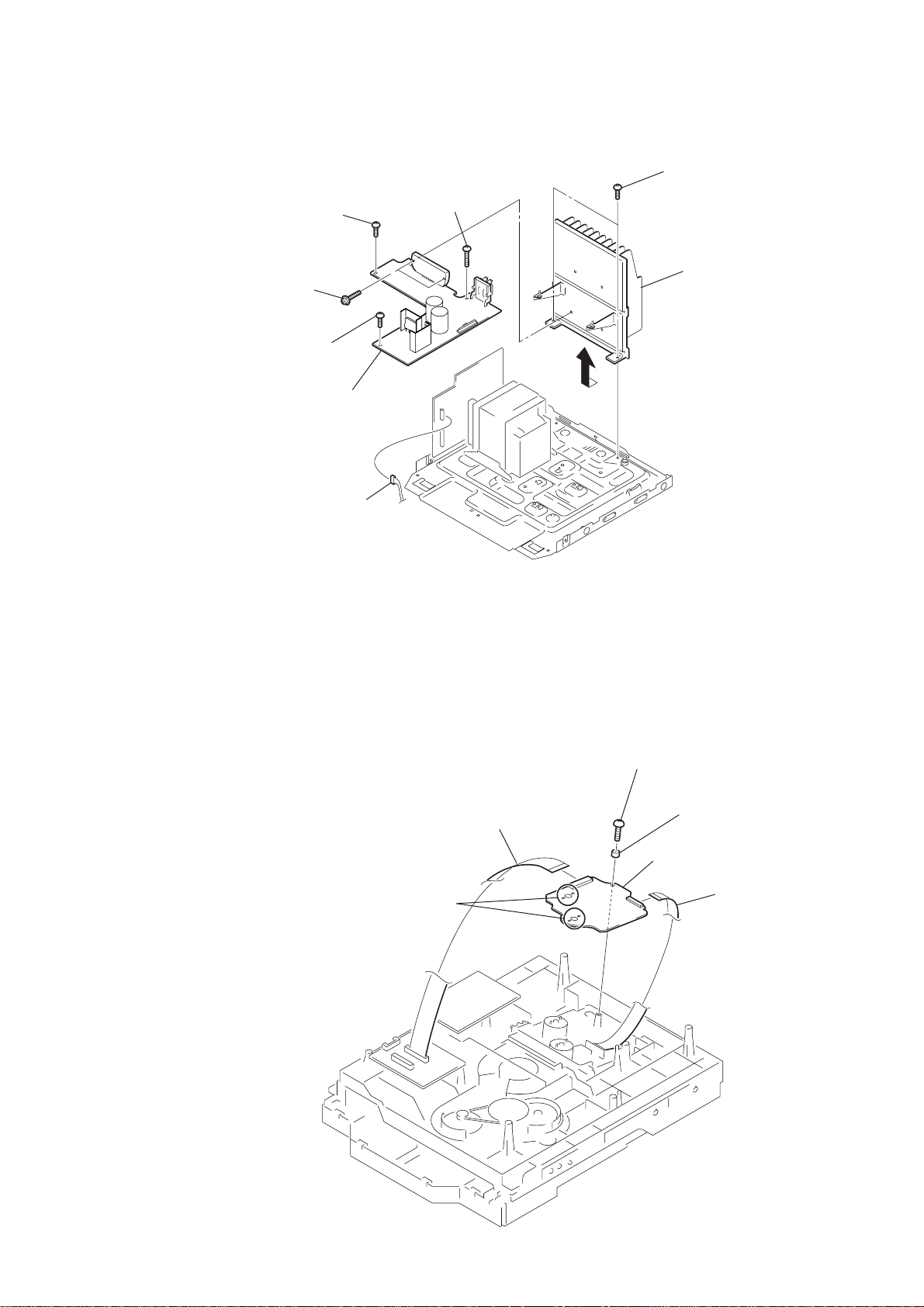
3-5. Tape Mechanism Deck, Game Jack Board........................ 12
3-6. Panel Board ....................................................................... 12
3-7. Back Panel Section, Sub Trans Board............................... 13
3-8. Trans Board .......................................................................13
3-9. Main Board ....................................................................... 14
3-10. Sub Woofer Board .............................................................14
3-11. Amp Board ........................................................................ 15
3-12. BD81A Board ................................................................... 15
3-13. Connect Board................................................................... 16
3-14. Driver Board, SW Board...................................................16
3-15. Optical Pick-up ................................................................. 17
3-16. Sensor Board ..................................................................... 17
3-17. Motor (TB) Board ............................................................. 18
3-18. Motor (LD) Board ............................................................. 18
4. TEST MODE ..................................................................... 19
5. DIAGRAMS
5-1. IC Pin Descriptions ........................................................... 22
5-2. Block Diagram –CD Section–........................................... 27
5-3. Block Diagram –Main Section–........................................ 28
5-4. Block Diagram –Panel/Power Section– ............................ 29
5-5. Block Diagram –Sub Woofer Section– ............................. 30
5-6. Circuit Boards Location .................................................... 30
5-7. Note for Printed Wiring Boards
and Schematic Diagrams .................................................. 31
5-8. Waveforms......................................................................... 31
5-9. Printed Wiring Board –CD Mechanism Section (1/2)– .... 32
5-10. Schematic Diagram –CD Mechanism Section (1/2)– ....... 33
5-11. Printed Wiring Boards –CD Mechanism Section (2/2)–... 34
5-12. Schematic Diagram –CD Mechanism Section (2/2)– ....... 35
5-13. Schematic Diagram –Main Section (1/2)– ........................36
5-14. Schematic Diagram –Main Section (2/2)– ........................37
5-15. Printed Wiring Board –Main Section– .............................. 38
5-16. Printed Wiring Boards –Panel Section– ............................ 39
5-17. Schematic Diagram –Panel Section (1/2)– ....................... 40
5-18. Schematic Diagram –Panel Section (2/2)– ....................... 41
5-19. Printed Wiring Boards –Jack Section–..............................42
5-20. Schematic Diagram –Jack Section– .................................. 43
5-21. Printed Wiring Board –Sub Woofer Section– ................... 44
5-22. Schematic Diagram –Sub Woofer Section– ...................... 45
5-23. Printed Wiring Board
–Power Amp Section (GX750/RX550)– ........................... 46
5-24. Printed Wiring Boards
–Transformer Section (GX750/RX550)– .......................... 47
5-25. Schematic Diagram –Power Section (GX750/RX550)–...48
5-26. Printed Wiring Board –Power Amp Section (RG551)– .... 49
5-27. Printed Wiring Boards –Transformer Section (RG551)–.. 50
5-28. Schematic Diagram –Power Section (RG551)–................ 51
5-29. IC Block Diagrams............................................................ 52
6. EXPLODED VIEWS
6-1. Main Section ..................................................................... 54
6-2. Front Panel Section (1)...................................................... 55
6-3. Front Panel Section (2)...................................................... 56
6-4. Front Panel Section (3)...................................................... 57
6-5. Main Board Section .......................................................... 58
6-6. CD Mechanism Section (1) ...............................................59
6-7. CD Mechanism Section (2) ...............................................60
7. ELECTRICAL PARTS LIST ........................................ 61
5
HCD-GX750/RG551/RX550
d
k
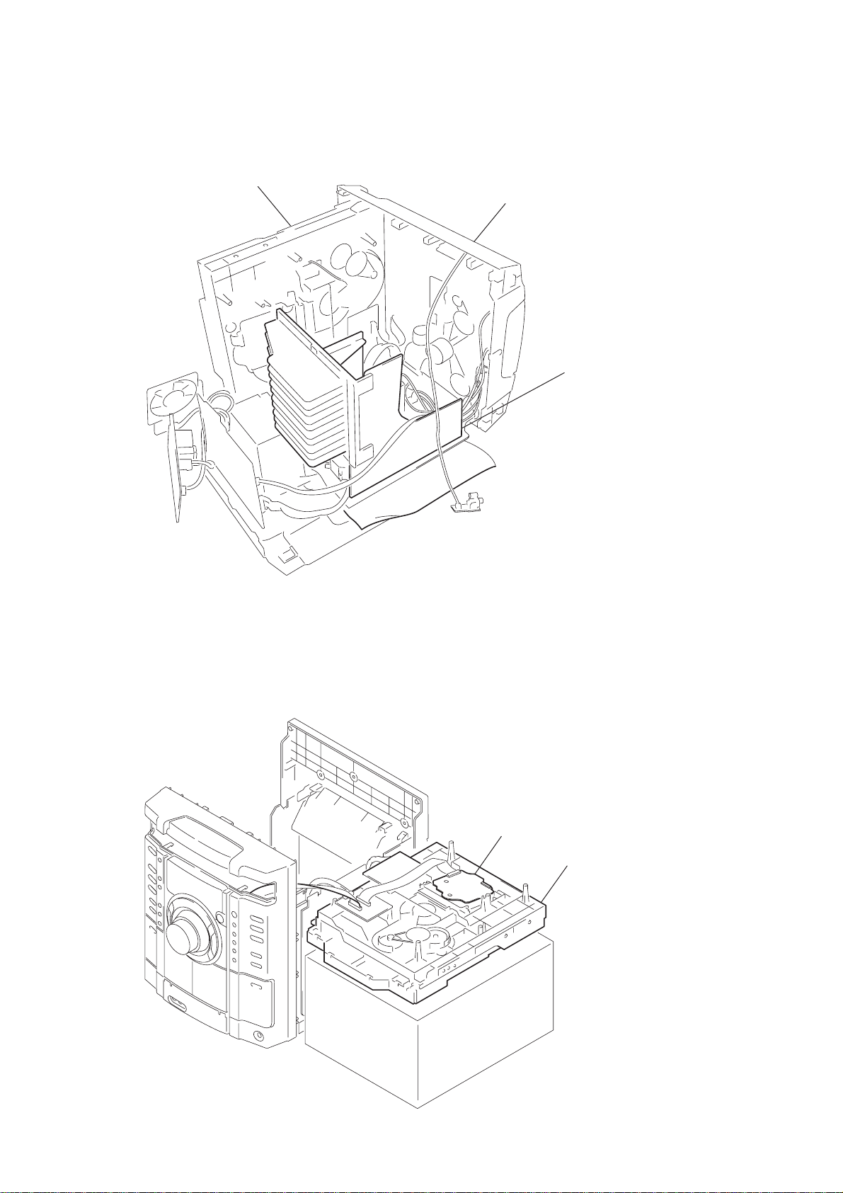
1-1. SERVICE POSITION-1 (AMP BOARD)
To inspect the AMP board, turn both of the front panel
and the CD mechanism deck so that the left side of the product faces down.
CD mechanism deck
SECTION 1
SERVICING NOTE
front panel
AMP boar
1-2. SERVICE POSITION-2 (BD81A BOARD)
Remove the CD mechanism deck and place it on top of the pedestal as shown.
Inspect the BD81A board in this set up.
BD81A board
CD mechanism dec
6
SECTION 2
GENERAL
HCD-GX750/RG551/RX550
This section is extracted
from instruction manual.
7
HCD-GX750/RG551/RX550
8
Note : Disassemble the unit in the order as shown below.
SET
3-1. CASE (TOP)
(Page 10)
3-2. CD DOOR
(Page 10)
3-3. FRONT PANEL SECTION
(Page 11)
HCD-GX750/RG551/RX550
SECTION 3
DISASSEMBLY
3-4. CD MECHANISM DECK
(Page 11)
3-12. BD81A BOARD
(Page 15)
3-15. OPTICAL PICK-UP
(Page 17)
3-7. BACK PANEL SECTION,
SUB TRANS BOARD
(Page 13)
3-8. TRANS BOARD
(Page 13)
3-5. TAPE MECHANISM DECK,
GAME JACK BOARD
(Page 12)
3-13. CONNECT BOARD
(Page 16)
3-14. DRIVER BOARD,
SW BOARD
(Page 16)
3-9. MAIN BOARD
(Page 14)
3-11. AMP BOARD
(Page 15)
3-6. PANEL BOARD
(Page 12)
3-16. SENSOR BOARD
(Page 17)
3-17. MOTOR (TB) BOARD
(Page 18)
3-18. MOTOR (LD) BOARD
(Page 18)
3-10. SUB WOOFER BOARD
(Page 14)
9
HCD-GX750/RG551/RX550
Note : Follow the disassembly procedure in the numerical order given.
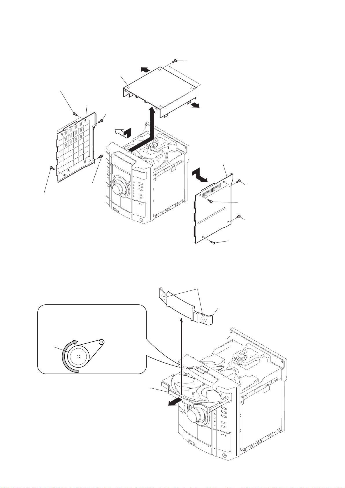
3-1. CASE (TOP)
qf
qh
case
(top)
7
two
screws
(case 3 TP2)
qs
0
(+BVTP 3
8
screw
(case 3 TP2)
screw
case (side-L)
9
screw
(+BVTP 3
×
10)
×
qg
10)
qa
qd
two
screws
(+BVTP 3
qf
5
×
10)
6
case (side-R)
3
(+BVTP 3
1
two
(case 3 TP2)
screw
screws
×
10)
3-2. CD DOOR
CD mechanism deck (CDM74)
1
Turn the pulley to the direction of the arrow.
pulley
Front panel side
2
Pull-out the disc tray.
3
two claws
2
(case 3 TP2)
4
CD door
4
(+BVTP 3
screw
screw
×
10)
10
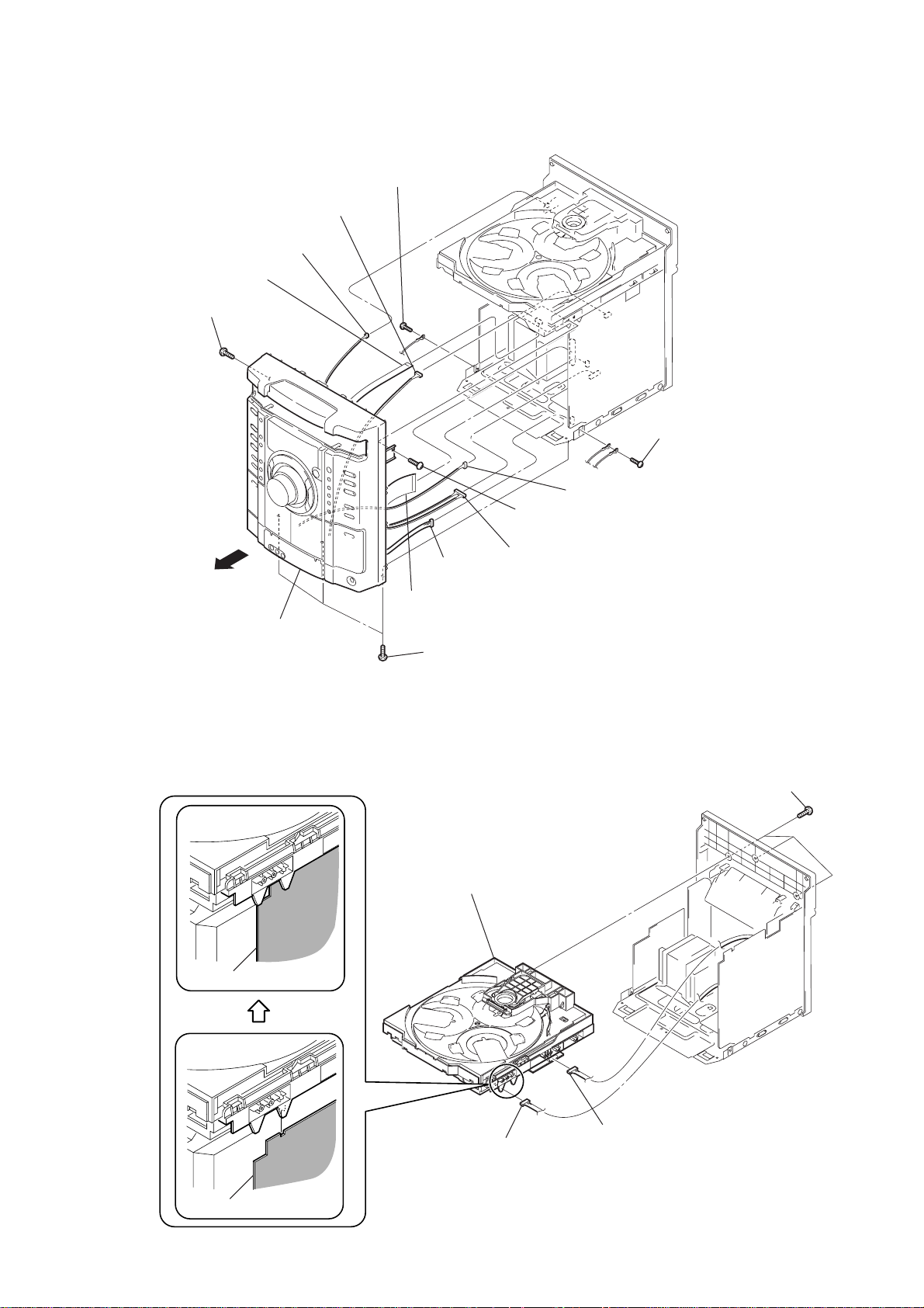
3-3. FRONT PANEL SECTION
1
3
CN823
8
screw
(+BVTP 3
×
10)
qa
CN805
CN314
4
screw
(+BVTP 3
×
HCD-GX750/RG551/RX550
8)
5
screw (+BVTP 3
×
8)
9
qf
front panel section
3-4. CD MECHANISM DECK
0
2
CN302
6
three
(+BVTP 3
7
screw (+BVTP 3
qd
CN309
screws
4
CN103
×
8)
CD mechanism deck
qs
CN102
×
10)
1
three
(+BVTP 3
screws
×
10)
MAIN board
MAIN board
3
CN874
2
CN701
11
HCD-GX750/RG551/RX550
)
)
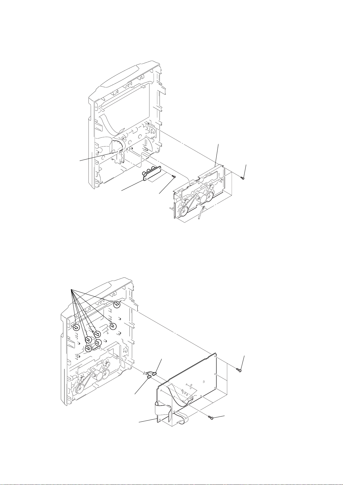
3-5. TAPE MECHANISM DECK, GAME JACK BOARD
1
connector
3
tape mechanism deck
2
six
screws
(+BVTP 2.6
×
8
3-6. PANEL BOARD
3
seven
claws
5
GAME JACK board
4
two
(+BVTP 2.6
screws
×
4
8)
CN604
1
eight
(+BVTP 2.6
screws
×
8
12
6
PANEL board
5
CN605
2
two
screws
(+BVTP 2.6
×
8)
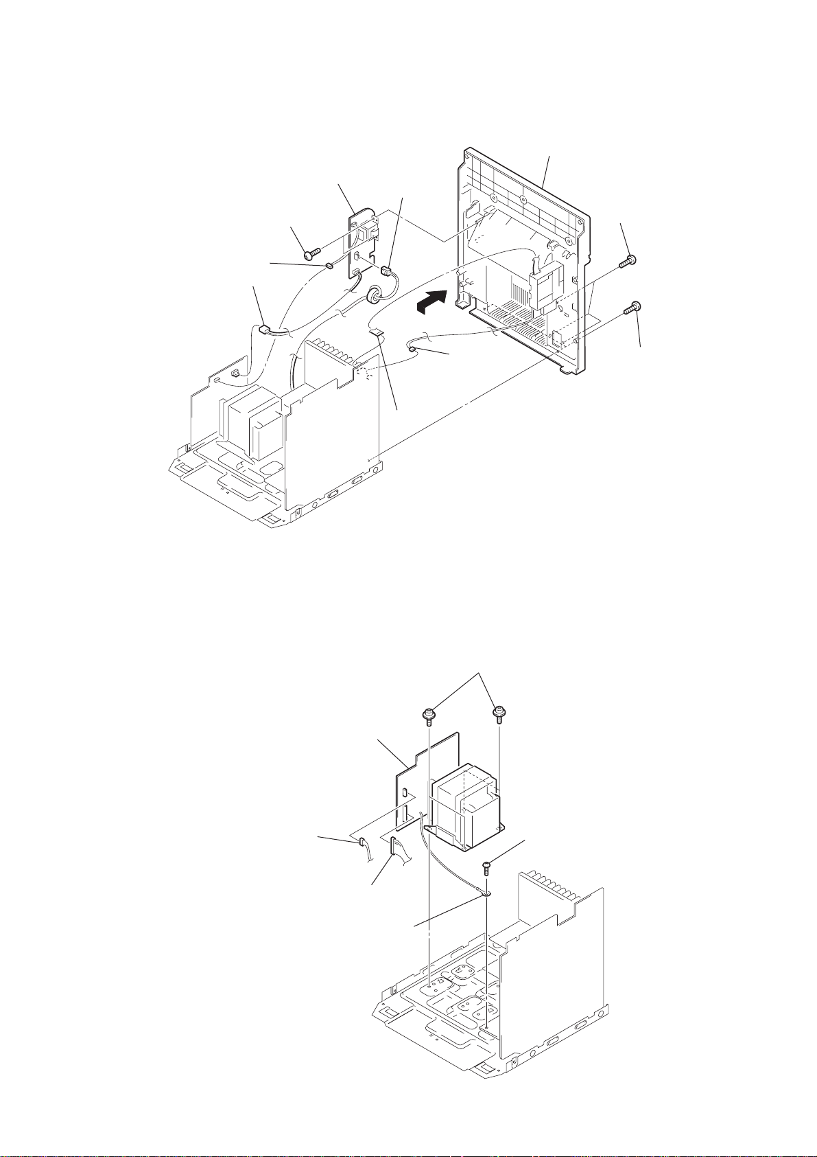
3-7. BACK PANEL SECTION, SUB TRANS BOARD
)
0
SUB TRANS board
3
4
2
9
CN906
1
two
screws
(+BVTP 3
CN904
×
10)
CN901
CN101
8
5
CN308
HCD-GX750/RG551/RX550
qa
back panel section
7
three
screws
×
screws
×
10)
10
(+BVTP 3
6
two
(+BVTP 3
3-8. TRANS BOARD
1
CN905
6
TRANS board
4
2
CN907
earth wire
5
four
screws
(+ITC 4
× 8
)
3
screw
(+BVIT 3
× 8R
)
13
HCD-GX750/RG551/RX550
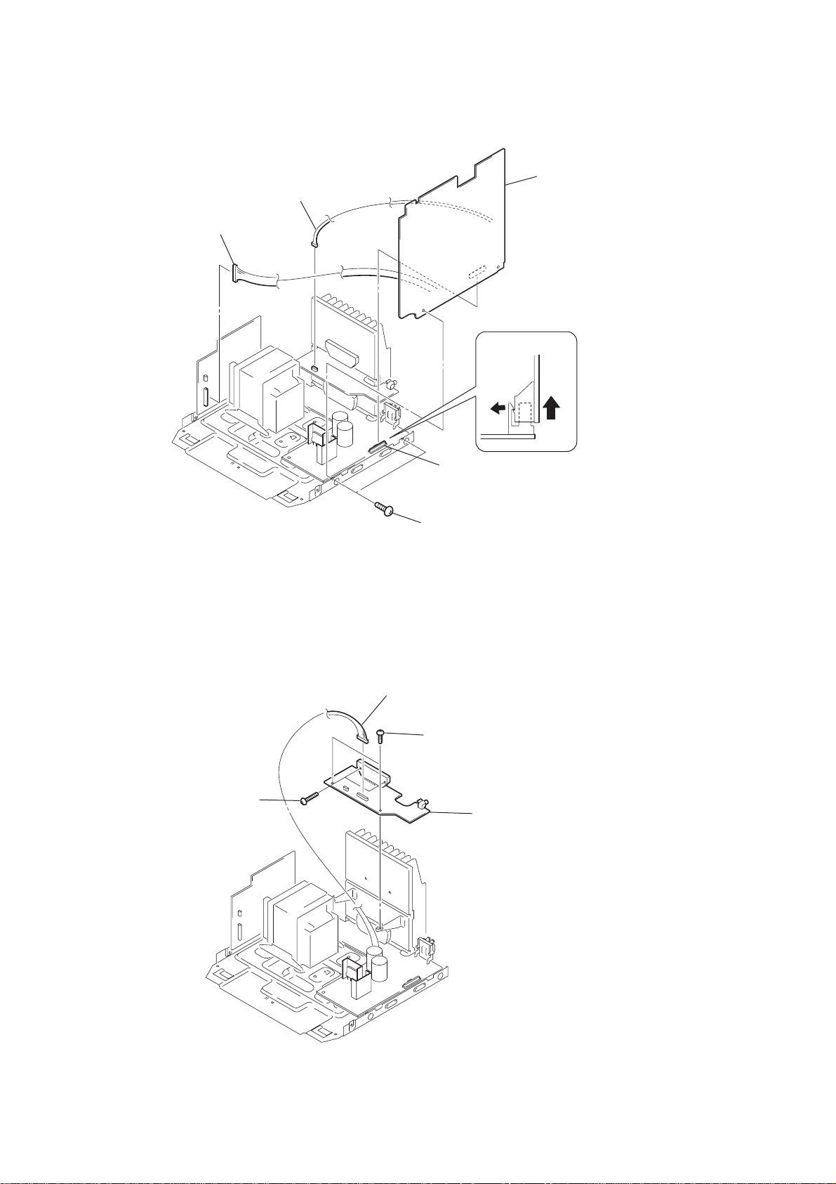
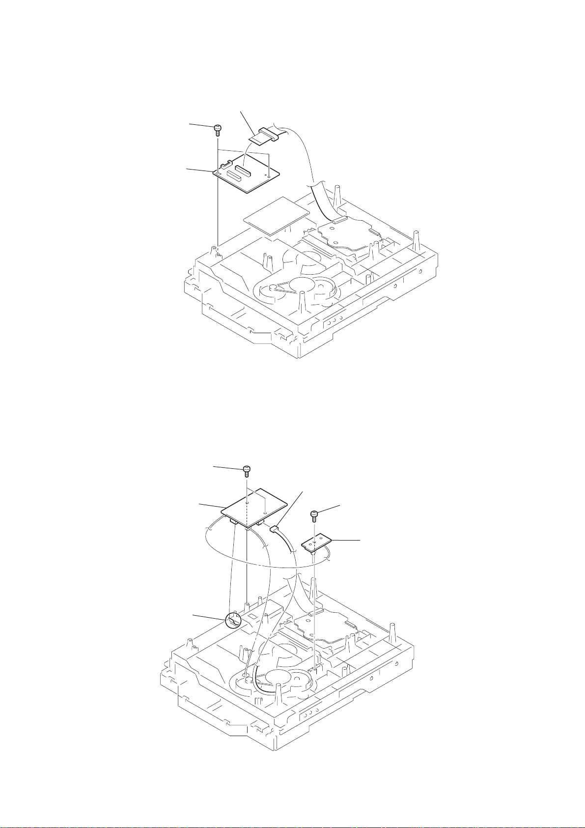
3-9. MAIN BOARD
1
CN907
2
CN501
5
MAIN board
MAIN board
3-10. SUB WOOFER BOARD
2
two
(transistor)
screws
1
3
CN502
3
4
CN441
two
screws
(+BVTP 3
two
screws
(+BVTP 3
4
×
8)
×
8)
SUB WOOFER board
14
3-11. AMP BOARD
)
4
6
two
(transistor)
5
screw
(+BVIT 3
screw
(+BVIT 3
screws
× 8R
× 8R
HCD-GX750/RG551/RX550
2
two
screws
3
screw
AMP
(+BVTP 3
board
)
)
9
×
14)
7
(+BVTP 4
8
×
heat sink
8
3-12. BD81A BOARD
5
Remove soldering from the four points.
1
CN905
1
CN202
3
screw
(+BVTP 2.6
6
BD81A
4
gap tube
× 8
board
2
CN101
)
15
HCD-GX750/RG551/RX550
3-13. CONNECT BOARD
2
two
screws
(+BVTP 2.6
3
CONNECT
× 8
board
1
CN871
)
3-14. DRIVER BOARD, SW BOARD
1
two
screws
(+BTTP (M2.6))
4
DRIVER
2
board
CN702
3
CN703
5
screw
(+BTTP (M2.6))
6
SW board
16
3-15. OPTICAL PICK-UP
)
2
h
older (213) ASSY
qd
optical pick-up
(KSM-215DCP/C2NP)
qa
two
insulators
0
two
coil springs
(insulator)
9
t
wo stoppers (BU)
8
t
wo screws
(BVTT M2.6)
qs
HCD-GX750/RG551/RX550
floating
screw
insulators
coil springs
7
6
(insulator)
5
4
screw
(BVTT M2.6)
3
floating
(+PTPWH M2.6)
screw
1
(+PTPWH M2.6
two
two
stopper (BU)
3-16. SENSOR BOARD
2
t
ray
1
floating
(+PTPWH M2.6)
6
floating
(+PTPWH M2.6)
7
g
screw
8
(+BTTP (M2.6))
screw
ear (geneva)
s
crew
0
SENSOR board
9
CN731
3
b
elt (table)
4
floating
p
ulley (table)
screw
(+PTPWH M2.6)
5
17
HCD-GX750/RG551/RX550
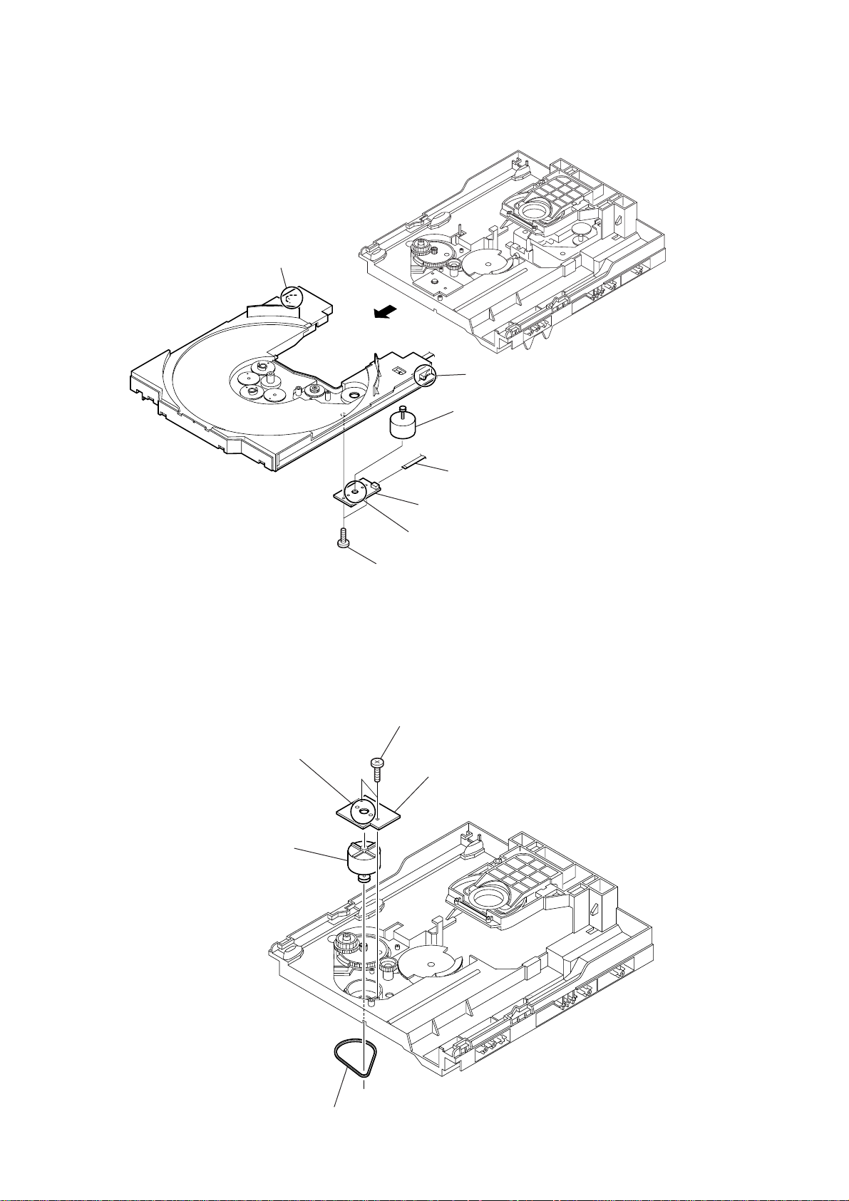
3-17. MOTOR (TB) BOARD
2
stopper
4
stopper
1
7
t
able motor assy (M741)
3-18. MOTOR (LD) BOARD
4
Remove the two solderings of motor.
5
l
oading motor assy (M751)
3
8
MOTOR (TB) board
6
Remove the two solderings of motor.
5
two
screws
(+BTTP (M2.6))
2
two
screws
(+BTTP (M2.6))
3
MOTOR (LD) board
CN742
18
1
b
elt (loading)
SECTION 4
TEST MODE
HCD-GX750/RG551/RX550
[Change-over of AM Tuner Step between 9 kHz and
10 kHz]
•A step of AM channels can be changed o ver between 9 kHz and
10 kHz.
Procedure:
1. Press ?/1 button to turn the set ON.
2. Select the function “TUNER”, and press TUNER/BAND
button to select the BAND “AM”.
3. Press ?/1 button to turn the set OFF.
4. Press TUNER/BAND and ?/1 buttons simultaneously, and
the display of fluorescent indicator tube changes to “AM 9 k
STEP” or “ AM 10 k STEP”, and thus the channel step is changed
over.
[Cold Reset]
• The cold reset clears all data including preset data stored in the
RAM to initial conditions. Execute this mode when returning
the set to the customer.
Procedure:
1. Press three buttons x , PLAY MODE/TUNING MODE ,
and DISC 1 simultaneously.
2. The fluorescent indicator tube displays “COLD RESET” and
the set is reset.
[Aging Mode]
This mode can be used for operation check of CD section and tape
deck section.
• If an error occurred:
The aging operation stops and is displayed status.
• If no error occurs:
The aging operation continues repeatedly.
1. Operating method of Aging Mode
Turn on the main power and select “CD” of the function.
1) Set three discs in tray. Select ALL DISCS, and REPEAT OFF .
2) Load the tapes recording use into both decks.
3) Press three buttons x , PLAY MODE/TUNING MODE ,
and EX-CHANGE simultaneously.
4) Aging operations of CD and tape are started at the same time.
5) To exit the aging mode, perform [Cold Reset].
2. Aging mode in CD section
1) Operation during aging mode
• In the agining mode, the program is excuted in the following
sequence.
(1) The disc tray opens and closes.
(2) The disc tray turns to select a disc 3.
(3) The pick-up accesses to the first track, and plays 3 seconds.
(4) The pick-up accesses to the last track, and plays 3 seconds.
(5) The disc tray opens and closes.
(6) The disc tray turns to select a disc 1.
(7) The same operation starts like step (3).
(8) After a disc 1 aging operation, a disc 2 is selected.
(9) When an aging operation of a disc 3 is completed, the display
“AGING
∗∗∗∗” value increases.
(10) If no error occurs, the aging operation continues repeatedly.
2) Error display
Disc error
Display Error
E00D01022 Focus error (No disc)
E00D02022 Sub Q error (Focus is good)
E00D02023 TOC reading error
E00D02014 Access error (Unable within regular time)
Mechanism error
Display Error
E00M__E_0 Error during opening tray
E00M__C_2 EX-CHANGE disc error
E00M__D_0 Error during closing tray
E00M__F_3 EX-OPEN error
E00M__D_5 EX-CLOSE error
E00M__C_2 Chuck-up error
E00M__C_3 Unchucking error
3. Aging mode in Tape Deck section
1) Operation during aging mode
• In the agining mode, the program is excuted in the following
sequence.
Step
1
Rewind the TAPE A
2
Rewind the TAPE B
3
Play the TAPE A (1 minute)
4
Stop the TAPE A (1 second)
5
Play the TAPE A (3 minutes)
6
Rewind(AMS) the TAPE A
7
F.F.(AMS) the TAPE A
8
Play the TAPE B (1 minute)
9
Stop the TAPE B (1 second)
10
Record the TAPE B (3 minutes)
11
Rewind(AMS) the TAPE B
12
F.F.(AMS) the TAPE B
Operation
Display
TAPE AAG-1
TAPE BAG-2
TAPE AAG-2
TAPE AAG-3
TAPE AAG-4
TAPE AAG-5
TAPE AAG-6
TAPE BAG-2
TAPE BAG-3
TAPE BAG-4
TAPE BAG-5
TAPE BAG-6
2) Error display
• If error occurred, the display remains like “TAPE BAG-2”.
4. Exiting from the aging mode
• Be sure to perform Cold Reset to exit from the aging mode.
19

HCD-GX750/RG551/RX550
[P ANEL T est Mode]
• All fluorecent segments and LEDs are tested.
•Keyboard check.
Procedure:
1. Press ?/1 button to turn the set ON.
2. To enter the test mode, press the three buttons x , PLAY
MODE/TUNING MODE and ENTER simultaneously.
3. All segments and LEDs (without STANDBY LED) are turned
on.
4. Press X and ENTER buttons simultaneously, and the key
check mode is activated.
5. The message “KEY 0 0 0 ” is displayed.
Each time a button is pressed, the key code number is displayed.
6. Press X and ENTER buttons simultaneously, and the key
count mode is activated.
7. The message “KEYCNT 0” is displayed.
Each time a button is pressed, “KEYCNT 0” value increased.
However, once a button is pressed, it is no longer taken into
account.
8. Press X and ENTER buttons simultaneously, and the head
phone detect mode is activated.
9. The message “H_P OFF” is displayed when a headphone jack
is not inserted.
“H_P ON ” is displayed when a headphone jack is inserted.
10. Press X and ENTER buttons simultaneously, and the volume
control detect mode is activated.
11. The message “VOLUME FLAT” is displayed.
“VOLUME UP” is displayed if rotating MASTER VOLUME
knob clockwise, or “VOLUME DOWN” is displayed if rotating
counterclockwise.
12. T o exit from the GC test mode after the head phone detect mode,
press X and ENTER buttons simultaneously.
[Version and Destination Display Mode]
•The version or destination is displayed.
Procedure:
1. Press ?/1 button to turn the set ON.
2. To enter the test mode, press the three buttons x , PLAY
MODE/TUNING MODE and DISC 2 simultaneously.
3. The destination is displayed.
4. Press DISPLAY buttons simultaneously.
5. The version is displayed.
6. To exit from this mode, press ?/1 button to turn the set OFF.
[CD Service Mode]
•This mode can run the CD sled motor freely. Use this mode, for
instance, when cleaning the pick-up.
Procedure:
1. Press ?/1 button to turn the set ON.
2. Select the function “CD”.
3. T o enter the test mode, press three b uttons x , PLAY MODE/
TUNING MODE , and Z simultaneously.
4. The CD service mode is selected.
5. With the CD in stop status, press M
pick-up to outside track, or press m button to inside track.
6. To exit from this mode, perform as follows:
1) Move the pick-up to the most inside track.
2) Press ?/1 button to turn the set OFF.
Note: • Always move the pick-up to most inside tr ack when exiting from
this mode. Otherwise, a disc will not be unloaded.
• Do not run the sled motor excessi vely, otherwise the gear can be
chipped.
button to move the
[MC T est Mode]
•This mode is used to test the function of the equalizer.
Procedure:
1. Press ?/1 button to turn the set ON.
2. To enter the test mode, press the three buttons x , PLAY
MODE/TUNING MODE and DISC 3 simultaneously.
3. Press the EQ + button.
The function of the equalizer is set to “MIN”.
4. Press the EQ – button.
The function of the equalizer is set to “MAX”.
5. Press the PRESET EQ button.
The function of the equalizer is set to “EQ FLAT”.
6. MASTER VOLUME up and down.
“VOLUME MIN” “VOLUME 16” “VOLUME MAX” is
displayed.
7. Press the GROOVE button.
The message “VACS OFF” or “VACS ON” is displayed.
8. To exit from this mode, press ?/1 button to turn the set OFF.
[CD Ship Mode (LOCK) ]
•This mode moves the pick-up to the position durable to vibra-
tion. Use this mode when returning the set to the customer after
repair.
Procedure:
1. Press ?/1 button to turn the set ON.
2. Select the function “CD”.
3. Press ?/1 button to turn the set OFF.
4. Press CD button and ?/1 button simultaneously.
5. The “STANDBY” display blinks instantaneously, and the CD
ship mode is set.
[CD Ship (LOCK) & COLD RESET MODE]
Procedure:
1. Press ?/1 button to turn the set ON.
2. Select the function “CD”.
3. Press ?/1 button to turn the set OFF.
4. Press three buttons x , CD and DISPLAY simultaneously .
5. The “STANDBY” display blinks instantaneously and CD ship
mode is set.
6. To fluorescent indicator tube displays “COLD RESET” and
the set is reset.
[Disc Tray Lock]
Procedure:
1. Press the ?/1 button to turn the set ON.
2. Press two buttons of x and Z simultaneously for five seconds.
3. The message “LOCKED” is displayed and the tray is locked.
(Even if exiting from this mode, the tray is still locked.)
4. Press two buttons of x and Z simultaneously for five seconds
again.
5. The message “UNLOCKED” is displayed and the tray is
unlocked.
6. To exit from this mode, press the ?/1 button to turn the set
OFF.
20

[CD Repeat 5 Times Limit Release Mode]
Procedure:
1. Press ?/1 button to turn the set ON.
2. Select the function “CD”.
3. Press three buttons x , CD and ENTER simultaneously.
4. The message “LIMIT OFF” is displayed.
5. Press ?/1 button the set OFF.
[AMP TEST MODE]
Procedure:
1. Press ?/1 button to turn the set ON.
2. To enter the test mode, press three buttons x , PLAY
MODE/TUNING MODE and ENTER simultaneously.
3. Press the DISPLAY button.
The message “V0 0 0” “ 000” is displayed.
4. Press the GROOVE button.
The message “DBFB ON” “DBFB OFF” is displayed.
5. Press the SURROUND button.
The message “SURROUND ON” “SURROUND OFF” is
displayed.
6. Press the EQ BAND button.
The message “LOW” “MID” “HIGH” is displayed.
7. Press ?/1 button to turn the set OFF.
HCD-GX750/RG551/RX550
21

HCD-GX750/RG551/RX550
SECTION 5
DIAGRAMS
5-1. IC PIN DESCRIPTIONS
• IC101 CXD3059AR (RF AMP) (BD81A BOARD)
Pin No. Pin Name I/O Pin Description
1MIRR I/O Mirror signal input/output Not used in this set. (Open)
2 DFCT I/O Defect signal input/output Not used in this set. (Open)
3 FOK I/O Focus OK signal input/output Not used in this set. (Open)
4 VSS — Internal digital ground pin
5 LOCK I/O
6 MDP O Spindle motor servo control signal output
7 SSTP I Disc innermost detection signal input
8IOVSS1 — I/O digital ground pin
9 SFDR O Sled drive signal output
10 SRDR O Sled drive signal output
11 TFDR O Tracking drive signal output
12 TRDR O Tracking drive signal output
13 FFDR O Focus drive signal output
14 FRDR O Focus drive signal output
15 IOVDD1 — I/O digital power supply pin (+3.3 V)
16 AVDD0 — Analog power supply pin (+3.3 V)
17 AVSS0 — Analog ground pin
18 NC — Not used. (Open)
19 E I E signal input
20 F I F signal input
21 TEI I Tracking error signal input
22 TEO O Tracking error signal output
23 FEI I Focus error signal input
24 FEO O Focus error signal output
25 VC O Center voltage output
26 A I A signal input
27 B I B signal input
28 C I C signal input
29 D I D signal input
30 NC — Not used. (Open)
31 AVDD4 — Analog power supply pin (+3.3 V)
32 RFDCO O RFDC signal output Not used in this set. (Open)
33 PDSENS I Reference voltage pin for PD Connect to ground in this set.
34 AC_SUM O RFAC summing amplifier signal output
35 EQ_IN I Equalizer circuit signal input
36 LD O APC amplifier signal output
37 PD I APC amplifier signal input
38 NC — Not used. (Open)
39 RFC I Equalizer cut-off frequency adjustment pin
40 AVSS4 — Analog ground pin
41 RFACO O RFAC signal output
42 RFACI I RFAC signal input or EFM signal input
43 AVDD3 — Analog power supply pin (+3.3 V)
44 BIAS I Asymmetry circuit constant current signal input
45 ASYI I Asymmetry comparator voltage signal input
46 ASYO O EFM full-swing signal output (Low=VSS, High=VDD)
47 VPCO O Wide-band EFM PLL charge pump signal output Not used in this set. (Open)
48 VCTL I Wide-band EFM PLL VCO2 control voltage signal input
49 AVSS3 — Analog ground pin
50 CLTV I Multiplier VCO1 control voltage signal input
GFS is sampled at 460Hz; when GFS is high , this pin outputs a high signal
If GFS is low eight consecutive
22

HCD-GX750/RG551/RX550
Pin No. Pin Name I/O Pin Description
51 FILO O Master PLL (slave=digital PLL) filter signal output
52 FILI I Master PLL filter signal input
53 PCO O Master PLL charge pump signal output
54 AVDD5 — Analog power supply pin (+3.3 V)
55 DDVROUT O DC/DC converter signal output
56 DDVRSEN I DC/DC converter output voltage monitor pin
57 AVSS5 — Analog ground pin
58 DDCR I DC/DC converter reset pin
59 NC — Not used. (Open)
60 BCKI I D/A interface bit clock signal input
61 PCMDI I D/A interface serial data signal input (2’s COMP, MSB first)
62 LRCKI I D/A interface LR clock signal input
63 LRCK O D/A interface LR clock signal output f=Fs
64 VSS — Internal digital ground pin
65 PCMD O D/A interface serial data signal output (2’s COMP, MSB first)
66 BCK O D/A interface bit clock signal output
67 VDD — Internal digital power supply pin (+3.3 V)
68 EMPH O High when the playback disc has emphasis, low it has not
69 EMPHI I High when de-emphasis is ON, low when input OFF
70 IOVDD2 — I/O digital power supply pin (+3.3 V)
71 DOUT O Digital signal output
72 TEST I Test pin Normally ground
73 TES1 I Test pin Normally ground
74 IOVSS2 — I/O digital ground pin
75 NC — Not used. (Open)
76 XVSS — Master clock ground pin
77 XTAO O Crystal oscillation circuit signal output (16.9 MHz)
78 XTAI I Crystal oscillation circuit signal input (16.9 MHz)
79 XVDD — Master clock power supply pin (+3.3 V)
80 AVDD1 — Analog power supply pin (+3.3 V)
81 AOUT1 O Lch analog signal output
82 VREFL O Lch reference voltage signal output
83 AVSS1 — Analog ground pin
84 AVSS2 — Analog ground pin
85 VREFR O Rch reference voltage signal output
86 AOUT2 O Rch analog signal output
87 AVDD2 — Analog power supply pin (+3.3 V)
88 NC — Not used. (Open)
89 IOVDD0 — I/O digital power supply pin (+3.3 V)
90 RMUT O Rch “0” detection flag Not used in this set. (Open)
91 LMUT O Lch “0” detection flag Not used in this set. (Open)
92 NC — Not used. (Open)
93 XTSL I Crystal selection input Not used in this set. (Connect to ground.)
94 IOVSS0 — I/O digital ground pin
95 XTACN I
96 SQSO O
97 SQCK I SQSO readout clock signal input
98 SBSO O Subcode P to W serial signal output Not used in this set. (Open)
99 EXCK I SBSO readout clock signal input Not used in this set. (Open)
100 XRST I System reset signal input “L”: Reset
101 SYSM I Mute signal input “H”: Mute Connect to ground in this set.
Oscillation circuit control signal input
Self-oscillation when high, oscillation stop when low
Subcode Q 80-bit and PCM peak and level data signal output
CD TEXT data signal output Not used in this set. (Open)
23
 Loading...