

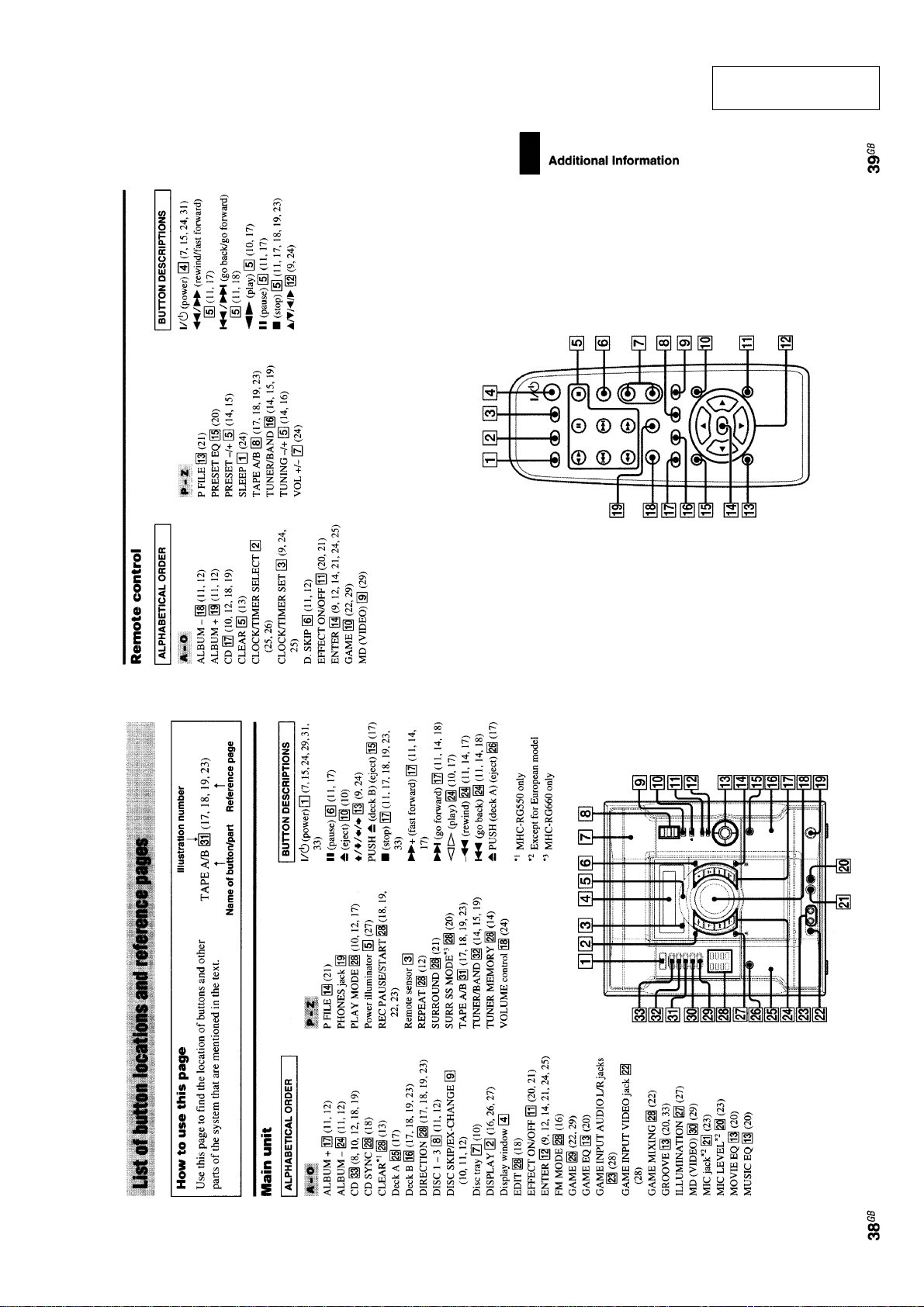
Page 1
HCD-RG550/RG660
SERVICE MANUAL
Ver 1.0 2003. 06
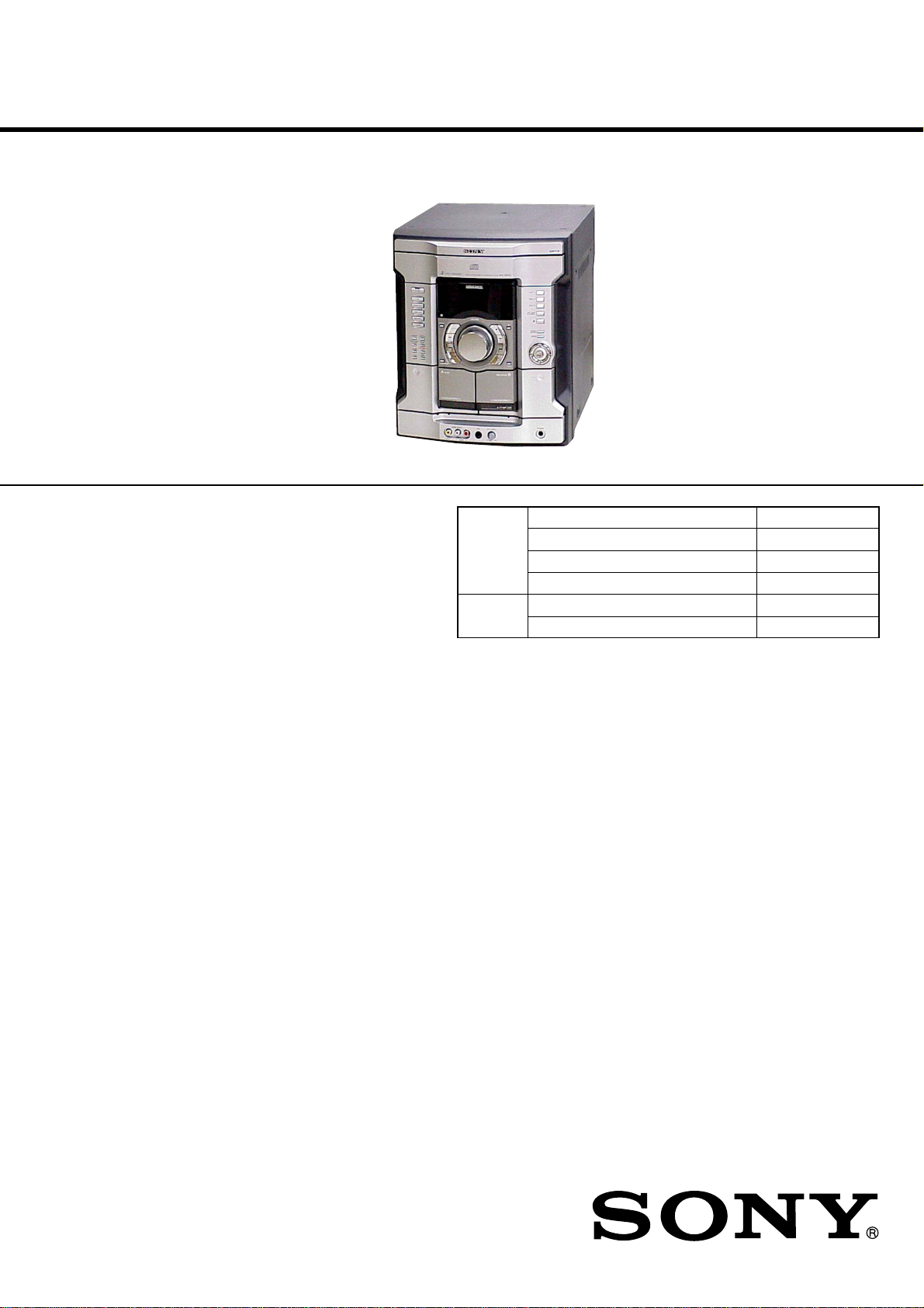
• HCD-RG550/RG660 is the
tuner, deck, CD and amplifier
section in MHC-RG550/RG660.
(Photo: HCD-RG550)
CD CD Mechanism Type CDM74F-K6BD71B
Section Base Unit Name BU-K6BD71B
Tape Deck Model Name Using Similar Machanism CX-JT8
Section Tape Transport Mechanism Type CWM43RR-23
AEP Model
UK Model
E Model
Model Name Using Similar Mechanism NEW
Optical Pick-up Name KSS-213DCP
Amplifier section
European model:
HCD-RG660:
Front speaker
DIN power output (rated):
160 + 160 watts
(6 ohms at 1 kHz, DIN)
Continuous RMS power output (reference):
200 + 200 watts (6 ohms at
1 kHz, 10% THD)
Music power output (reference):
400 + 400 watts (6 ohms at
1 kHz, 10% THD)
Other models:
HCD-RG660:
The following measured at AC 120, 127, 220, 240 V,
50/60 Hz
DIN power output (rated):
160 + 160 watts
(6 ohms at 1 kHz, DIN)
Continuous RMS power output (reference):
200 + 200 watts (6 ohms at
1 kHz, 10% THD)
HCD-RG550:
The following measured at AC 120, 127, 220, 240 V,
50/60 Hz
DIN power output (rated):
115 + 115 watts
(6 ohms at 1 kHz, DIN)
Continuous RMS power output (reference):
140 + 140 watts (6 ohms at
1 kHz, 10% THD)
SPECIFICATIONS
Inputs
MD (VIDEO) IN L/R (phono jacks):
voltage 450/250 mV,
impedance 47 kilohms
GAME INPUT AUDIO L/R (phono jacks):
voltage 250 mV,
impedance 47 kilohms
GAME INPUT VIDEO (phono jack):
1 Vp-p, 75 ohms
MIC (phone jack) (except for European model):
sensitivity 1 mV,
impedance 10 kilohms
Outputs
PHONES (stereo mini jack):
accepts headphones of
8 ohms or more
VIDEO OUT (phono jack):
max. output level
1 Vp-p, unbalanced, Sync
negative, load impedance
75 ohms
SPEAKER: accepts impedance of 6 to
16 ohms
SURROUND SPEAKER (HCD-RG660 only):
accepts impedance of 24
ohms
– Continued on next page –
COMPACT DISC DECK RECEIVER
9-961-000-01
2003F04-1
© 2003. 06
Sony Corporation
Home Audio Company
Published by Sony Engineering Corporation
1
Page 2

HCD-RG550/RG660
CD player section
System Compact disc and digital
audio system
Laser Semiconductor laser
(λ=780 nm)
Emission duration:
continuous
Frequency response 2 Hz – 20 kHz (±0.5 dB)
Wavelength 780 – 790 nm
Signal-to-noise ratio More than 90 dB
Dynamic range More than 90 dB
CD OPTICAL DIGITAL OUT
(square optical connector jack, rear panel)
Wavelength 660 nm
Output –18 dBm
Tape deck section
Recording system 4-track 2-channel stereo
Frequency response 50 – 13,000 Hz (±3 dB),
using Sony TYPE I
cassettes
Wow and flutter ±0.15% W.Peak (IEC)
0.1% W.RMS (NAB)
±0.2% W.Peak (DIN)
Tuner section
FM stereo, FM/AM superheterodyne tuner
FM tuner section
Tuning range 87.5 – 108.0 MHz
Antenna FM lead antenna
Antenna terminals 75 ohms unbalanced
Intermediate frequency 10.7 MHz
AM tuner section
Tuning range
Latin American model: 530 – 1,710 kHz (with the tuning
interval set at 10 kHz)
531 – 1,710 kHz (with the tuning
interval set at 10 kHz)
European, Middle Eastern and Philippine models:
531 – 1,602 kHz (with the tuning
interval set at 9 kHz)
Other models: 530 – 1,710 kHz (with the tuning
interval set at 10 kHz)
531 – 1,602 kHz (with the tuning
interval set at 9 kHz)
Antenna AM loop antenna
Antenna terminals External antenna terminal
Intermediate frequency 450 kHz
General
Power requirements
European model: 230 V AC, 50/60 Hz
Argentine model: 220 V AC, 50/60 Hz
Mexican model: 127 V AC, 60 Hz
Saudi Arabian model: 120 – 127 V/220 V or
230 – 240 V AC,
50/60 Hz
Adjustable with voltage
selector
Other models: 120 V, 220 V or 230 –
240 V AC, 50/60 Hz
Adjustable with voltage
selector
Power consumption
European model:
HCD-RG660: 190 watts
0.35 watts (at the Power
Saving Mode)
Other models:
HCD-RG660: 190 watts
HCD-RG550: 135 watts
Dimensions (w/h/d) Approx. 280 × 325 × 407 mm
Mass
European model:
HCD-RG660: Approx. 10.0 kg
Other models:
HCD-RG660: Approx. 11.0 kg
HCD-RG550: Approx. 9.0 kg
Supplied accessories: AM loop antenna (1)
Remote Commander (1)
Batteries (2)
FM lead antenna (1)
Speaker pads
HCD-RG660 (16)
HCD-RG550 (8)
Design and specifications are subject to change without
notice.
Speaker
Front speaker SS-RG665 for HCD-RG660/RG550:
Speaker system 3-way, 3-unit, bass-reflex
type
Speaker units
Sub Woofer: 15 cm, cone type
Woofer: 15 cm, cone type
Tweeter: 5 cm, cone type
Nominal impedance 6 ohms
Dimensions (w/h/d) Approx. 240 × 363 × 290 mm
Mass Approx. 4.7 kg net per
speaker
Surround speaker SS-RS660 for HCD-RG660:
Speaker system 3-way, 3-unit, bass-reflex
type
Speaker units
Woofer: 13 cm, cone type
Tweeter: 5 cm, cone type
Super tweeter: 2 cm, dome type
Nominal impedance 24 ohms
Dimensions (w/h/d) Approx. 195 × 325 × 225 mm
Mass Approx. 2.3 kg net per
speaker
SAFETY-RELATED COMPONENT WARNING!!
COMPONENTS IDENTIFIED BY MARK 0 OR DOTTED LINE
WITH MARK 0 ON THE SCHEMATIC DIAGRAMS AND IN
THE PARTS LIST ARE CRITICAL TO SAFE OPERATION.
REPLACE THESE COMPONENTS WITH SONY P ARTS WHOSE
PART NUMBERS APPEAR AS SHOWN IN THIS MANUAL OR
IN SUPPLEMENTS PUBLISHED BY SONY.
2
Page 3
HCD-RG550/RG660
CAUTION
Use of controls or adjustments or performance of procedures
other than those specified herein may result in hazardous
radiation exposure.
Notes on Chip Component Replacement
• Never reuse a disconnected chip component.
• Notice that the minus side of a tantalum capacitor may be
damaged by heat.
Flexible Circuit Board Repairing
• Keep the temperature of soldering iron around 270°C during
repairing.
• Do not touch the soldering iron on the same conductor of the
circuit board (within 3 times).
• Be careful not to apply force on the conductor when soldering
or unsoldering.
NOTES ON HANDLING THE OPTICAL PICK-UP BLOCK
OR BASE UNIT
The laser diode in the optical pick-up block may suffer electrostatic
breakdown because of the potential difference generated by the
charged electrostatic load, etc. on clothing and the human body.
During repair, pay attention to electrostatic break-down and also
use the procedure in the printed matter which is included in the
repair parts.
The flexible board is easily damaged and should be handled with
care.
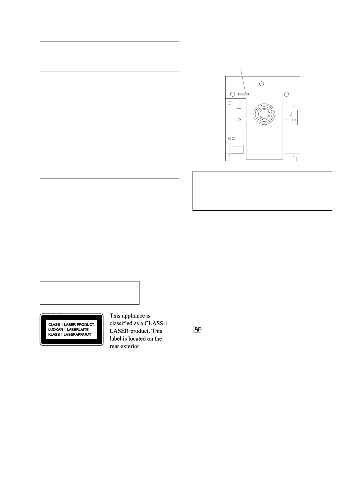
NOTES ON LASER DIODE EMISSION CHECK
The laser beam on this model is concentrated so as to be focused on
the disc reflective surface by the objective lens in the optical pickup block. Therefore, when checking the laser diode emission,
observe from more than 30 cm away from the objective lens.
Laser component in this product is capable
of emitting radiation exceeding the limit for
Class 1.
MODEL IDENTIFICATION
– BACK PANEL –
PARTS No.
MODEL PARTS No.
RG550: E2, E3, E51 4-247-996-01
RG550: MX 4-247-996-11
RG660: E3 4-247-996-21
RG660: AEP , UK 4-247-996-31
• Abbreviation
E2 : 120 V AC area in E model
E3 : 240 V AC area in E model
E51 : 220 V AC area in E model
MX : Mexican model
LASER DIODE AND FOCUS SEARCH OPERATION
CHECK
Carry out the “S curve check” in “CD section adjustment” and check
that the S curve waveforms is output three times.
UNLEADED SOLDER
Boards requiring use of unleaded solder are printed with the lead
free mark (LF) indicating the solder contains no lead.
(Caution: Some printed circuit boards may not come printed with
the lead free mark due to their particular size)
SETTING AND RELEASING THE CD DISC TRAY LOCK
FUNCTION
This set has a disc tray lock function to prevent discs for
demonstration at shops from theft. While this lock function is set,
the tray will not be delivered out even when the OPEN/CLOSE
button is pressed.
Setting method:
Press the OPEN/CLOSE button while pressing the STOP button.
After a few seconds, the message “LOCKED” will appear on the
fluorescent indicator tube with the tray locked.
Releasing method:
Just as the lock is set, press the OPEN/CLOSE button while
pressing the STOP button.
After a few seconds, the message “UNLOCKED” will appear with
the lock released.
: LEAD FREE MARK
Unleaded solder has the following characteristics.
• Unleaded solder melts at a temperature about 40 °C higher than
ordinary solder.
Ordinary soldering irons can be used but the iron tip has to be
applied to the solder joint for a slightly longer time.
Soldering irons using a temperature regulator should be set to about
350 °C.
Caution: The printed pattern (copper foil) may peel away if the
heated tip is applied for too long, so be careful!
• Strong viscosity
Unleaded solder is more viscou-s (sticky , less prone to flo w) than
ordinary solder so use caution not to let solder bridges occur such
as on IC pins, etc.
• Usable with ordinary solder
It is best to use only unleaded solder but unleaded solder may also
be added to ordinary solder.
3
Page 4

HCD-RG550/RG660
TABLE OF CONTENTS
1. GENERAL
Main Unit ................................................................................ 5
Remote Control ....................................................................... 5
2. DISASSEMBLY
2-1. Case (Top) ........................................................................... 7
2-2. CD Door .............................................................................. 7
2-3. CD Mechanism Block ......................................................... 8
2-4. Front Panel Section ............................................................. 9
2-5. Tape Mechanism Deck ...................................................... 10
2-6. Panel Board, 6 Stream Led Board, Remote Board............ 10
2-7. Jack Board .........................................................................11
2-8. Back Panel Section............................................................ 11
2-9. Main Board ....................................................................... 12
2-10. Power Amp Board ............................................................. 12
2-11. SW Board, Driver Board...................................................13
2-12. CD Block Assy.................................................................. 13
2-13. Sensor Board ..................................................................... 14
2-14. Motor (TB) Board ............................................................. 14
2-15. Motor (LD) Board ............................................................. 15
2-16. BD Board .......................................................................... 15
2-17. Optical Pick-up ................................................................. 16
3. TEST MODE ..................................................................... 17
4. ELECTRICAL ADJUSTMENTS................................. 20
6. EXPLODED VIEWS
6-1. Main Section .....................................................................52
6-2. Front Panel Section (1)...................................................... 53
6-3. Front Panel Section (2)...................................................... 54
6-4. Front Panel Section (3)...................................................... 55
6-5. Main Board Section .......................................................... 56
6-6. CD Mechanism Deck Section (1) ..................................... 57
6-7. CD Mechanism Deck Section (2) ..................................... 58
6-8. Base Unit Section ..............................................................59
7. ELECTRICAL PARTS LIST ........................................ 60
5. DIAGRAMS
5-1. IC Pin Descriptions ........................................................... 21
5-2. Block Diagram –CD Section–........................................... 25
5-3. Block Diagram –Tuner/Tape/Panel Section– ....................26
5-4. Block Diagram –Amp/Power Supply Section–................. 27
5-5. Circuit Boards Location .................................................... 28
5-6. Note for Printed Wiring Boards
and Schematic Diagrams .................................................. 29
5-7. Waveforms......................................................................... 29
5-8. Printed Wiring Board –CD Mechanism Section (1/2)– .... 30
5-9. Schematic Diagram –CD Mechanism Section (1/2)– ....... 31
5-10. Printed Wiring Boards –CD Mechanism Section (2/2)– ...32
5-11. Schematic Diagram –CD Mechanism Section (2/2)– ....... 33
5-12. Schematic Diagram –Main Section (1/4)– ........................34
5-13. Schematic Diagram –Main Section (2/4)– ........................35
5-14. Schematic Diagram –Main Section (3/4)– ........................36
5-15. Schematic Diagram –Main Section (4/4)– ........................37
5-16. Printed Wiring Board –Main Section– .............................. 38
5-17. Printed Wiring Boards –Panel Section– ............................ 39
5-18. Schematic Diagram –Panel Section– ................................ 40
5-19. Printed Wiring Boards –Jack Section–..............................41
5-20. Schematic Diagram –Jack Section– .................................. 42
5-21. Printed Wiring Board –Power Amp Section– ................... 43
5-22. Schematic Diagram –Power Amp Section (1/2)– ............. 44
5-23. Schematic Diagram –Power Amp Section (2/2)– ............. 45
5-24. Printed Wiring Board
–Transformer Section (HCD-RG550)– ............................. 46
5-25. Printed Wiring Board
–Transformer Section (HCD-RG660)– ............................. 47
5-26. Schematic Diagram –Transformer Section– ..................... 48
5-27. IC Block Diagrams............................................................ 49
4
Page 5
SECTION 1
GENERAL
HCD-RG550/RG660
This section is extracted
from instruction manual.
5
Page 6
HCD-RG550/RG660
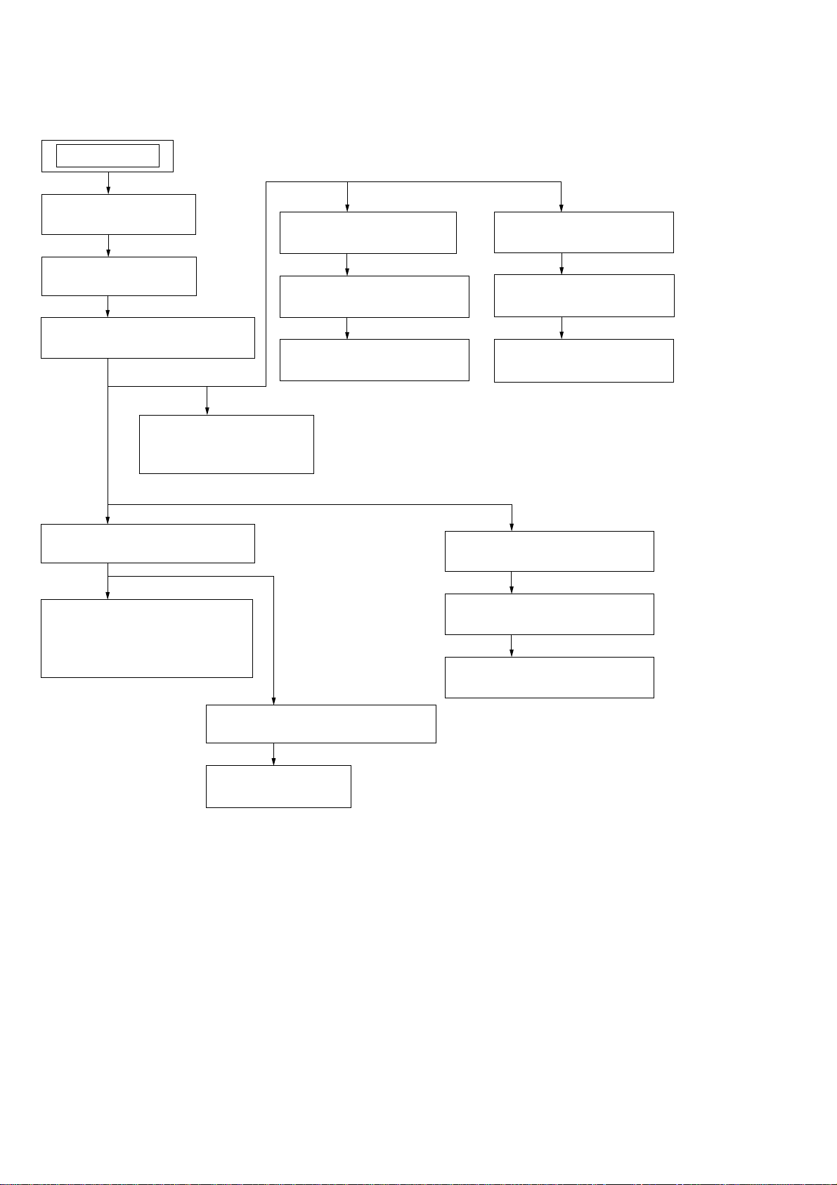
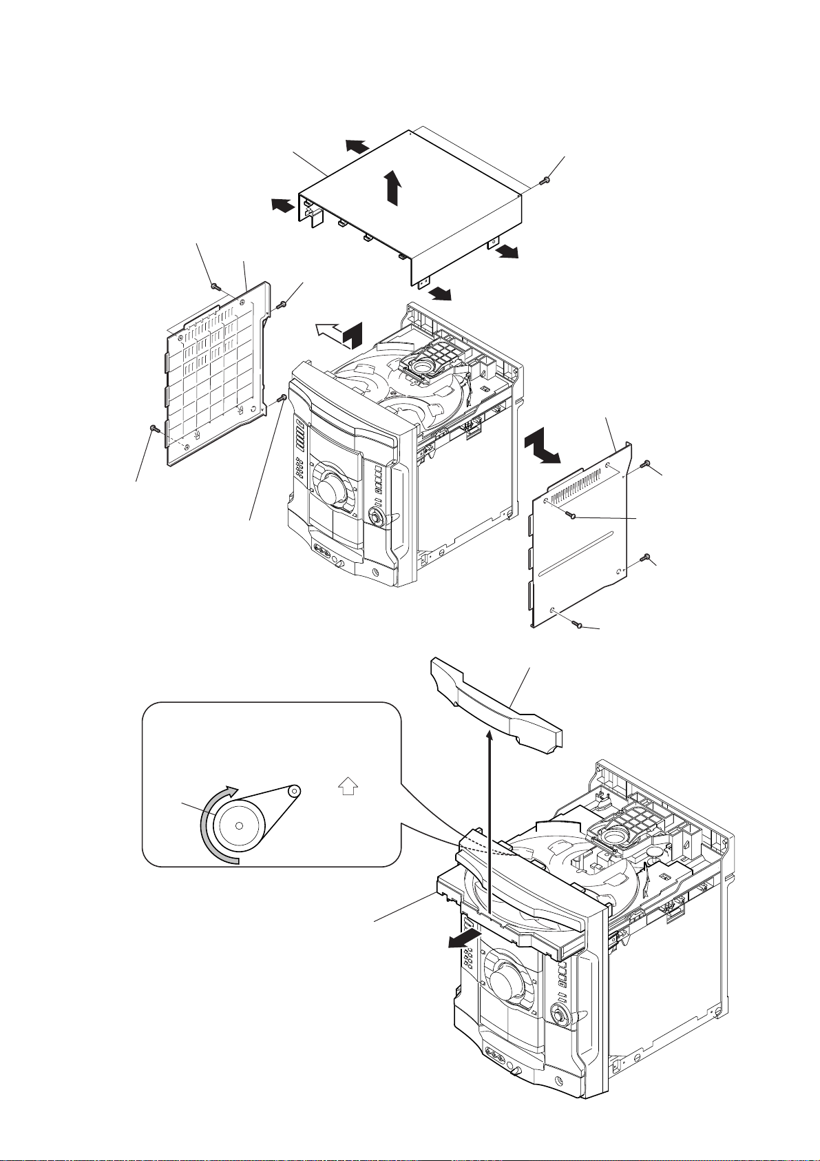
Note : Disassemble the unit in the order as shown below.
SET
2-1. CASE (TOP)
(Page 7)
2-2. CD DOOR
(Page 7)
2-3. CD MECHANISM BLOCK
(Page 8)
2-11. SW BOARD,
DRIVER BOARD
(Page 13)
2-13. SENSOR BOARD
2-14. MOTOR (TB) BOARD
2-15. MOTOR (LD) BOARD
SECTION 2
DISASSEMBLY
(Page 14)
(Page 14)
(Page 15)
2-12. CD BLOCK ASSY
(Page 13)
2-16. BD BOARD
(Page 15)
2-17. OPTICAL PICK-UP
(Page 16)
2-4. FRONT PANEL SECTION
(Page 9)
2-6. PANEL BOARD,
6 STREAM LED BOARD,
REMOTE BOARD
(Page 10)
2-5. TAPE MECHANISM DECK
2-7. JACK BOARD
2-8. BACK PANEL SECTION
(Page 11)
2-9. MAIN BOARD
(Page 12)
2-10. POWER AMP BOARD
(Page 12)
(Page 10)
(Page 11)
6
Page 7
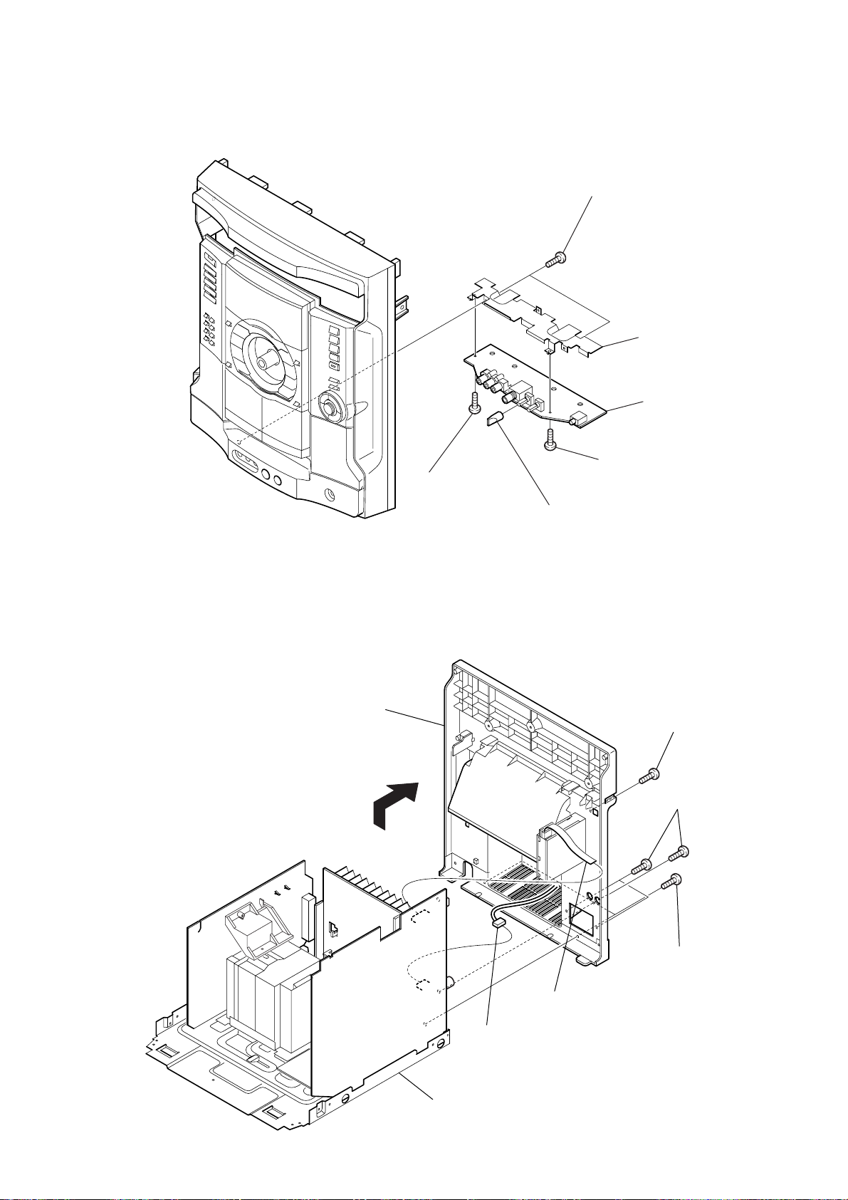
Note : Follow the disassembly procedure in the numerical order given.
)
2-1. CASE (TOP)
HCD-RG550/RG660
6
two screws (case 3 TP2)
7
screw (case 3 TP2)
9
(+BVTP 3
qf
case (side-L)
screw
case (top)
qs
×
10)
qs
8
screw
(+BVTP 3
×
q;
10)
qd
qs
qs
qa
two screws (+BVTP 3
case (side-R)
5
×
10)
3
screw
(+BVTP 3
1
two screws
(case 3 TP2)
×
10
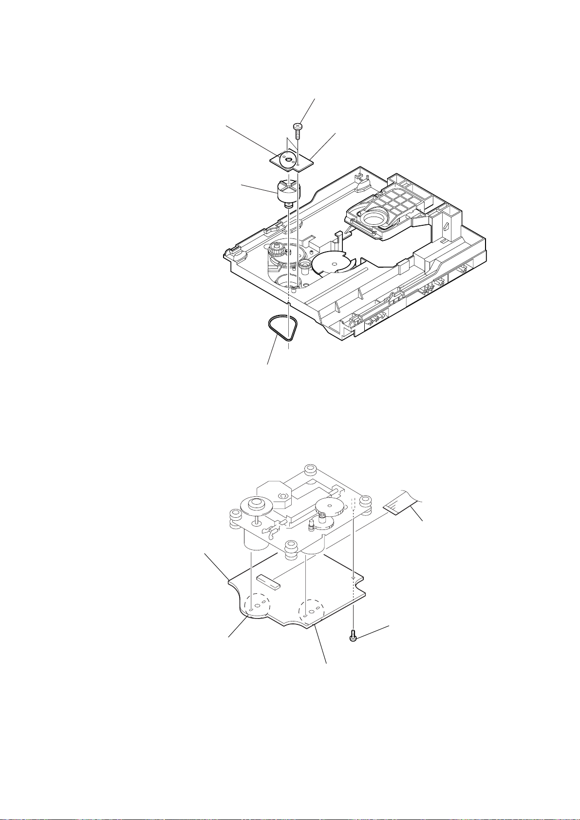
2-2. CD DOOR
CD mechanism deck (CDM74F-K6BD71B)
1
Turn the pulley to the direction of arrow.
pulley
Front panel side
2
Pull-out the disc tray.
3
4
CD door
4
(+BVTP 3
2
screw (case 3 TP2)
screw
×
10)
7
Page 8
HCD-RG550/RG660
)
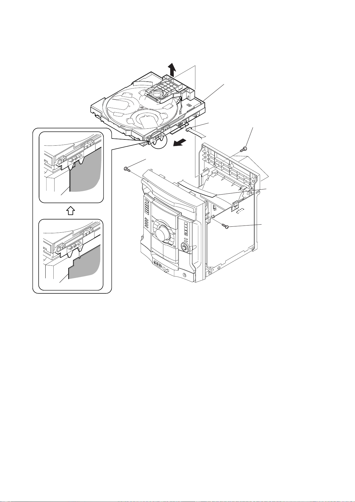
2-3. CD MECHANISM BLOCK
5
3
screw
(+BVTP 3
6
8
CD mechanism block
1
CN701
×
10)
2
three
(+BVTP 3
screws
×
10)
MAIN board
MAIN board
7
CN312
(flat type)
4
screw
(+BVTP 3
×
10
8
Page 9
2-4. FRONT PANEL SECTION
)
8
screw
(+BVTP 3
3
×
8)
TRANS board
CN311
(flat type)
1
CN003
HCD-RG550/RG660
4
CN305
qa
front panel section
2
7
connector
6
connector
0
three screws (+BVTP 3
5
CN304
(flat type)
CN310
× 8
9
screw
(+BVTP 3
)
×
8
9
Page 10
HCD-RG550/RG660
)
)
2-5. TAPE MECHANISM DECK
1
connector
2
(+BVTP 2.6
5
tape mechanism deck
two
screws
3
(+BVTP 2.6
×
three
8)
screws
×
4
(+BVTP 2.6
8)
two
screws
×
8
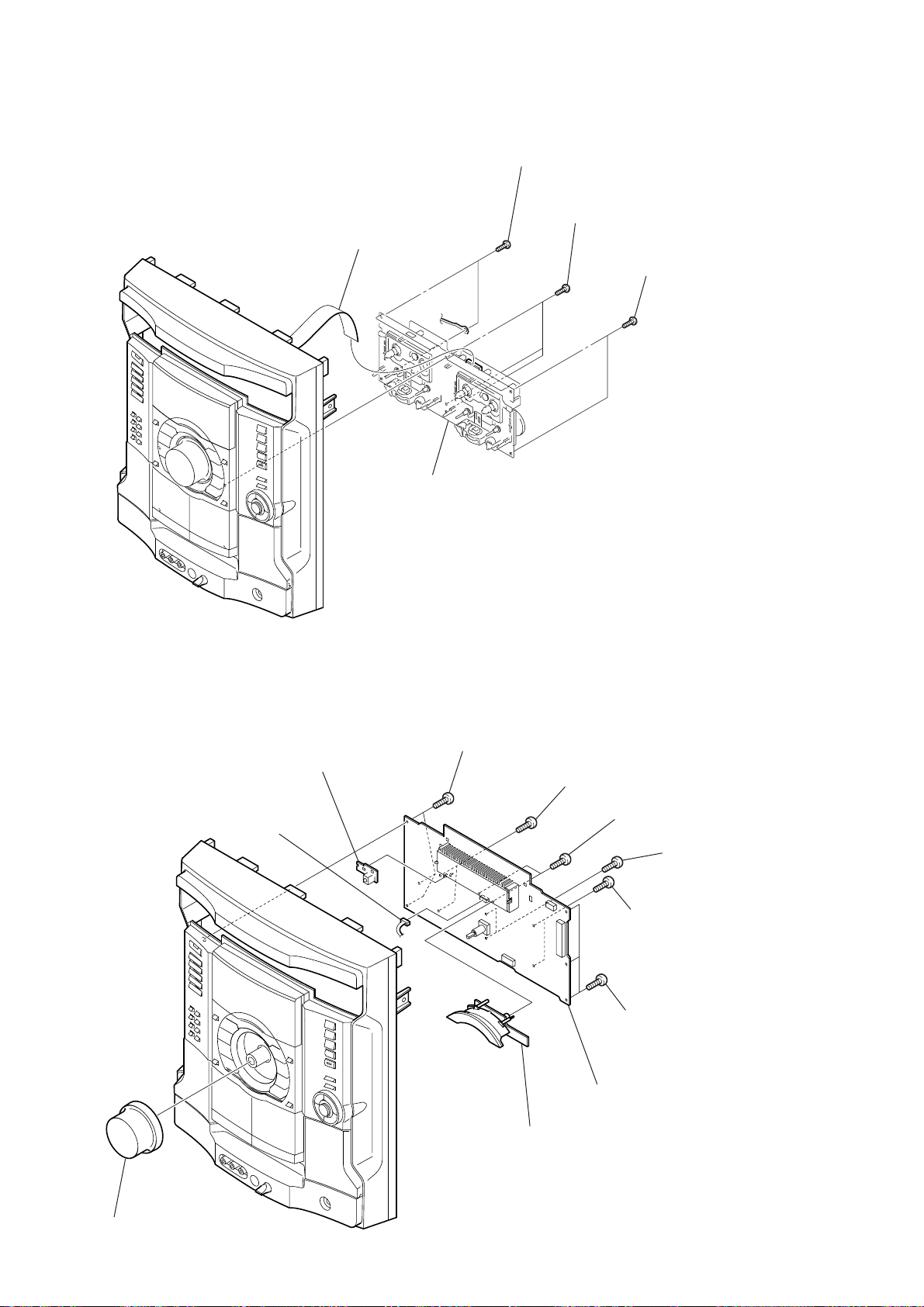
2-6. PANEL BOARD, 6 STREAM LED BOARD, REMOTE BOARD
5
three
(+BVTP 2.6
0
CN607
qa
REMOTE board
screws
×
8)
6
two
(+BVTP 2.6
9
6 STREAM LED board
screws
×
8
two
(+BVTP 2.6
3
two
(+BVTP 2.6
2
three
(+BVTP 2.6
7
PANEL board
8)
screws
×
8)
4
two
screws
(+BVTP 2.6
screws
×
screws
×
×
8
8)
8)
10
1
volume knob
Page 11
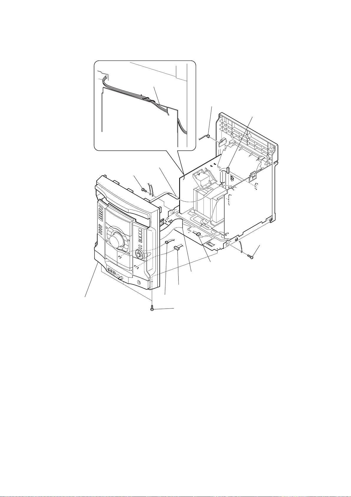
2-7. JACK BOARD
HCD-RG550/RG660
1
two
screws
(+BVTP 2.6
4
shield plate
6
×
8)
JACK board
2-8. BACK PANEL SECTION
7
back panel section
6
2
screw
(+BVTP 3
×
3
screw
(+BVTP 3
8)
5
two mic knobs
×
8)
5
screw
(+BVTP 3
4
three
(+BVTP 3
×
screws
×
10)
10)
2
CN303
chassis section
1
CN101
(flat type)
3
two
screws
(+BVTT 3
×
8)
11
Page 12
HCD-RG550/RG660
d
d
2-9. MAIN BOARD
MAIN board
2
MAIN boar
2-10. POWER AMP BOARD
1
CN902
4
(+BVTP 3
5
screw
(+BVTP 3
screw
×
8)
×
8)
3
screw
(+BVTT 3
×
10)
1
(+BVTP 3
two claws
2
screw
(+BVTT 3
6
POWER AMP boar
two
screws
×
10)
×
10)
12
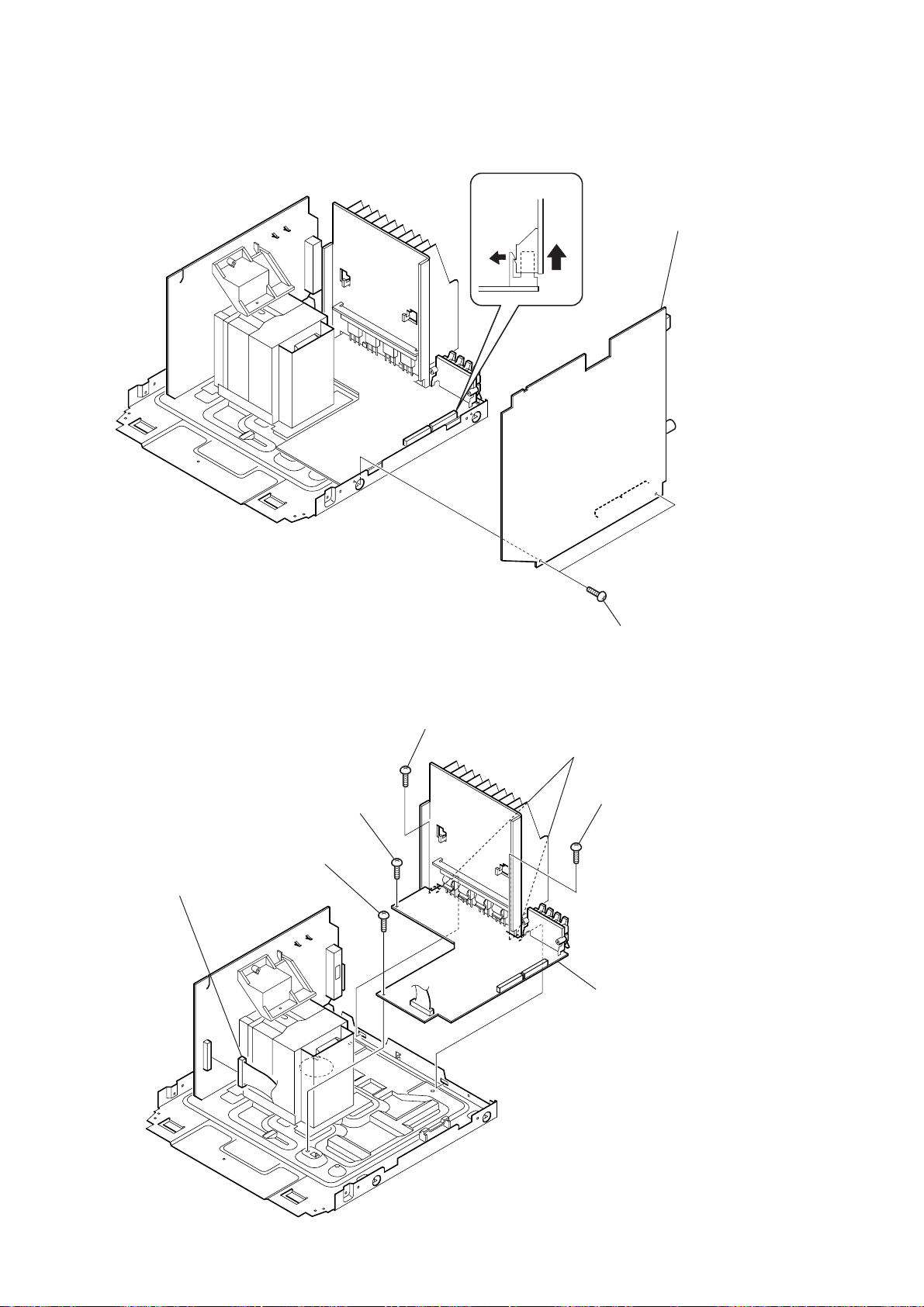
Page 13
2-11. SW BOARD, DRIVER BOARD
d
2
SW board
7
CN702 (flat type)
4
CN703
6
DRIVER boar
HCD-RG550/RG660
2-12. CD BLOCK ASSY
3
1
screw
(+BTTP (M2.6))
2
holder (213) assy
qd
CD block assy
qa
two
insulators
CN704
5
two
screws
(+BTTP (M2.6))
qs
1
floating
(+PTPWH M2.6)
7
two
insulators
coil springs
5
(insulator)
screw
0
two
coil springs
(insulator)
9
two stoppers (BU)
8
(+BTTB M2.6)
two screws
4
stopper (BU)
3
screw
(+BTTB M2.6)
6
floating
(+PTPWH M2.6)
screw
13
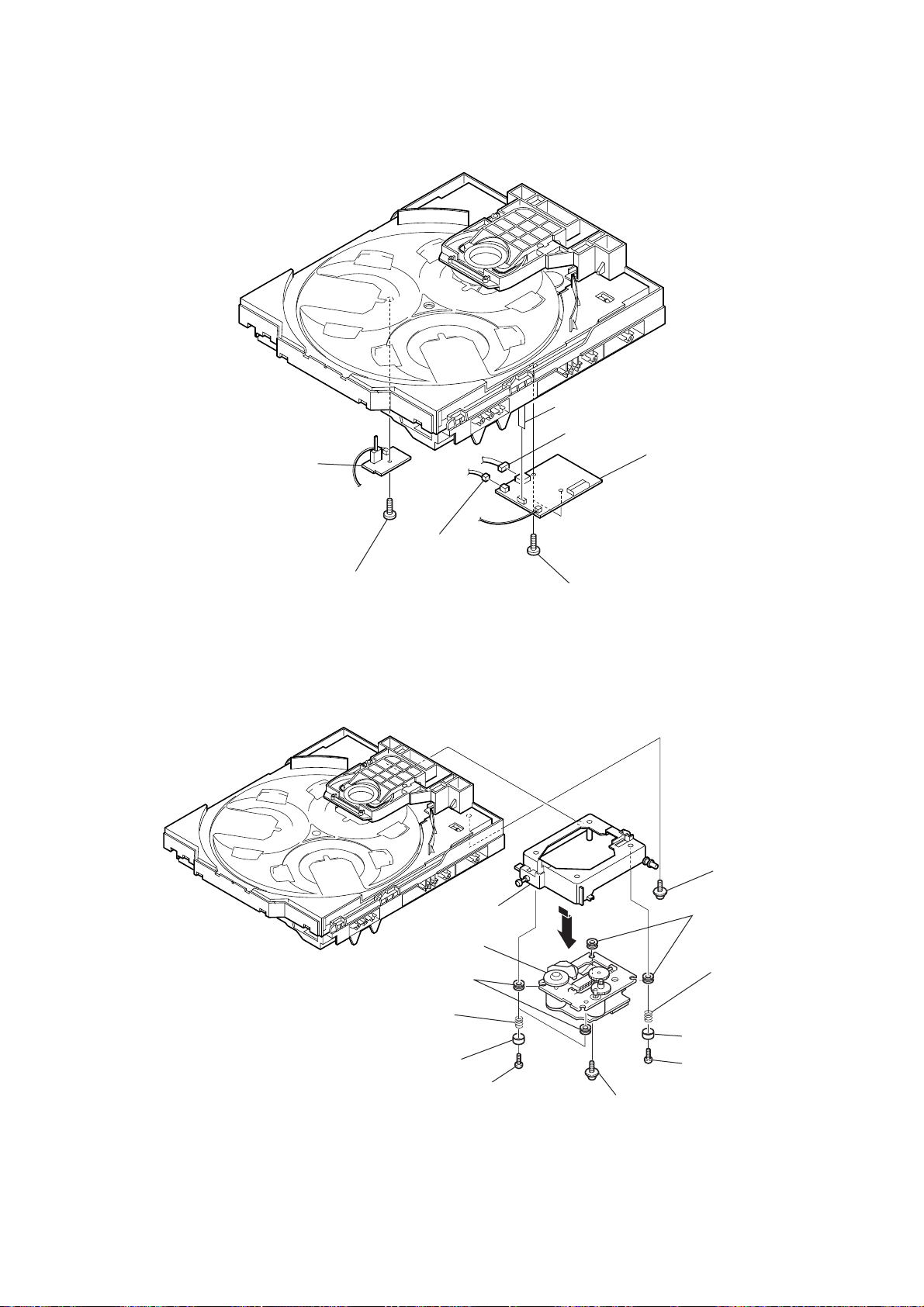
Page 14
HCD-RG550/RG660
2-13. SENSOR BOARD
2
tray
1
floating
(+PTPWH M2.6)
6
floating
(+PTPWH M2.6)
7
gear (geneva)
screw
8
screw
(+BTTP (M2.6))
screw
9
SENSOR board
0
CN731
3
belt (table)
4
floating
(+PTPWH M2.6)
5
screw
pulley (table)
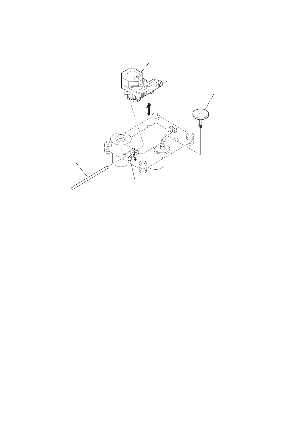
2-14. MOTOR (TB) BOARD
claw
1
claw
5
table motor assy (M741)
3
MOTOR (TB) board
4
Remove the two solderings of motor.
14
2
two
screws
(+BTTP (M2.6))
Page 15
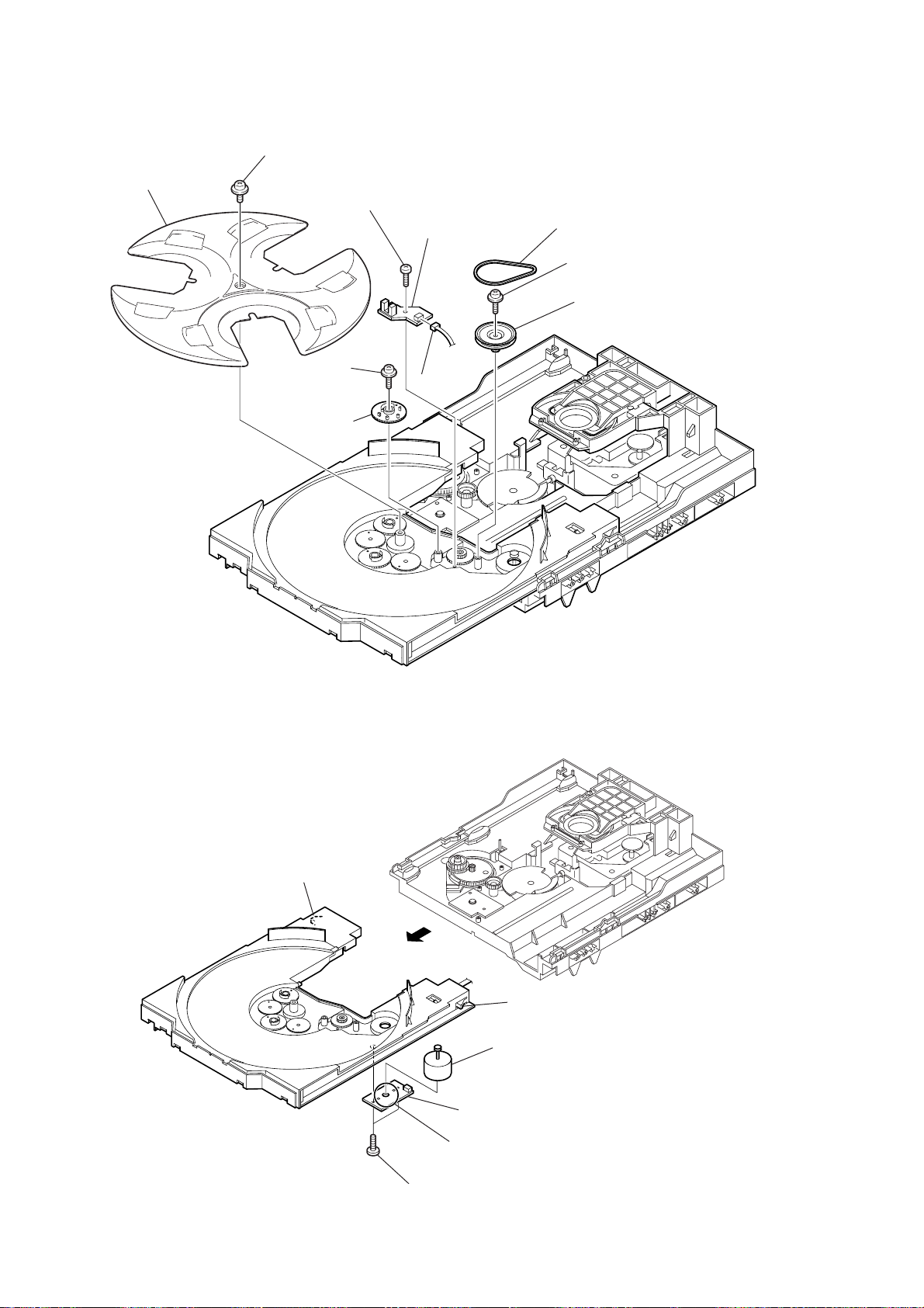
)
2-15. MOTOR (LD) BOARD
4
Remove the two solderings of motor.
5
loading motor assy (M751)
2
two
screws
(+BTTP (M2.6))
3
MOTOR (LD) board
HCD-RG550/RG660
2-16. BD BOARD
2
1
4
BD board
Remove the two solderings of motor.
belt (loading)
5
1
screw
(+BVTP 3
CN708 (flat type
×
8)
3
Remove the two solderings of motor.
15
Page 16
HCD-RG550/RG660
2-17. OPTICAL PICK-UP
3
Remove the optical pick-up
(KSS-213D) in the direction
of arrow
B
B
.
1
gear (A)
2
sled shaft
A
1
Slide the lever
in the direction of arrow
A
.
16
Page 17

SECTION 3
TEST MODE
HCD-RG550/RG660
[COLD RESET]
• The cold reset clears all data including preset data stored in the
RAM to initial conditions. Execute this mode when returning the
set to the customer.
Procedure:
1. Press the [POWER] key to turn the power ON.
2. Press three keys of x , [GROOVE] and [POWER] simultaneously.
3. The message “COLD RESET” is displayed on the fluorescent
indicator tube momentarily, then becomes standby states.
[TUNER STEP CHANGE-OVER]
(Except AEP and UK models)
•A step of AM channels can be changed over between 9 kHz and
10 kHz.
Procedure:
1. Press the [POWER] key to turn the power ON.
2. Press the [TUNER BAND] key to select “AM”.
3. Press the [POWER] key to turn the power OFF.
4. Press two keys of [ENTER] and [POWER] simultaneously.
5. The message “9K STEP” or “10K STEP” is displayed on the
fluorescent indicator tube, and thus the channel step is changed
over.
[CD SHIP MODE]
•This mode moves the optical pick-up to the position durable to
vibration. Use this mode when returning the set to the customer
after repair.
Procedure:
1. Press the [POWER] key to turn the power ON.
2. Press the [CD] key to select “CD”.
3. Press two keys of [CD] and [POWER] simultaneously.
4. The message “LOCK” is displayed on the fluorescent indicator
tube, and the CD ship mode is set.
[CHANGE-OVER FUNCTION OF MD/VIDEO]
•This mode is used to enable function of external input to change
over between MD and VIDEO.
Procedure:
1. Set to standby state.
2. Press two keys of [MD VIDEO ] and [POWER] simultaneously.
3. The message “MD” or “VIDEO” is displayed on the fluorescent
indicator tube, and the function of external input is changed
over.
(
)
[CD TRAY LOCK MODE]
•This mode is used to unable to take sample disc out of tray in the
shop.
Procedure:
1. Press the [POWER] key to turn the power ON.
2. Press the [CD] key to select “CD”.
3. Set disc on the tray.
4. While pressing the x key, press the Z key for 5 seconds.
5. The message “LOCKED” is displayed on the fluorescent
indicator tube and the tray is locked. (Even if pressing
the Z key, the message “LOCKED” is displayed on the
fluorescent indicator tube and the tray is locked)
6. To release from this mode, while pressing the x key, press
the Z key for 5 seconds.
7. The message “UNLOCKED” is displayed on the fluorescent
indicator tube and the tray is unlocked.
[AMP TEST MODE]
•This mode is used to set the parameter of AMP IC for adjustment
of tone quality and VACS level and display VACS status.
Procedure:
1. Press the [POWER] key to turn the power ON.
2. Press three keys of x , [GAME EQ] and [EFFECT ON/OFF]
simultaneously.
3. When the AMP test mode is activated, the message “AMP
TEST” is displayed on the fluorescent indicator tube
momentarily.
4. Press two keys of [GAME EQ] and [DISC 2] simultaneously, mode
is changed over to parameter setting of AMP IC and display of
VACS status.
5. When the VACS status, the message VACS level, VACS signal
level, and VACS signal hold le vel is displayed on the fluorescent
indicator tube.
6. Press the [GROOVE] key, DBFB ON/OFF is changed over.
7. Press the [GAME MIXING] key, surround ON/OFF is changed
over.
8. Press the cursol B and b key, EQ band is changed over to
LOW, MID or HIGH.
9. Press the cursol V and v key, EQ curve adjustment value is
changed over between –8dB to +8dB.
10. To release from this mode, press two keys of [GAME EQ] and
[MOVIE EQ] simultaneously.
17
Page 18
HCD-RG550/RG660
[AGING MODE]
• This mode can be used for operation check of CD section and
tape deck section.
CD section and tape deck section work in parallel.
If an error occurred:
The aging operation stops only an error occurred sections and
display then status.
If no error occurs:
The aging operation continues repeatedly.
Procedure:
1. Press the [POWER] key to turn the power ON.
2. Press the [CD] key to select “CD”.
3. Set disc on the tray and set tape into the deck.
4. Set the “ALL DISCS” mode and “REV OFF” mode.
5. Press three keys of x , [GAME EQ] and [DISC SKIP/EX-CHANGE]
simultaneously.
6. The message “AGING” is displayed on the fluorescent
indicator tube momentarily, then aging operations of CD and
tape are started at the same time.
7. To release from this mode, operate the “COLD RESET”.
1. Display at the Aging Mode
Display operating state of CD section and tape deck section
alternately.
If an error occurred, stop display which that section.
2. CD Section
The sequence during the aging mode is following as below.
Display at the aging mode is the same as the normal operation.
Aging mode sequence (CD section) :
3. Tape Deck Section
The sequence during the aging mode is following as below.
If an error occurred, stop display that step.
Aging mode sequence (tape deck section) :
Rewind the tape A and B
“AAG-1 or 2”
Shut off
FWD play the tape A
“AAG-3”
2 minutes
Fast forward the tape A
“AAG-4”
Shut off or 20 seconds
REV play the tape A
“AAG-5”
2 minutes
Rewind the tape A
“AAG-6”
Shut off
FWD play the tape B
“BAG-3”
Start (from disc 1)
Disc chucking
TOC read
Play first track for 2 seconds
Play last track for 2 seconds
EX-change open/close
Open the disc tray
Disc skip
Close the tray
Change the next disc.
2 minutes
Fast forward the tape B
“BAG-4”
Shut off or 20 seconds
REV play the tape B
“BAG-5”
2 minutes
Rewind the tape B
“BAG-6”
Shut off
Note: “*AG-*” is display of each step.
18
Page 19

HCD-RG550/RG660
[GC TEST MODE]
• This mode is used to check the fluorescent indicator tube, LED
and key.
Procedure:
1. Press the [POWER] key to turn the power ON.
2. Press three keys of x , [GAME EQ] and [DISC 2] simultaneously.
3. Fluorescent indicator tube and LEDs are all turned ON.
4. Press two keys of [GAME EQ] and [DISC 2] simultaneously, mode
is changed over.
5. In the key check mode, press each key, the defined key number
of every each key list is displayed on the fluorescent indicator
tube.
6. In the key count check mode, “KEYCNT 0” is displayed on the
fluorescent indicator tube. Each time a key is pressed,
“KEYCNT” value increases. Howev er , once a key is pressed , it
is no longer taken into account.
7. In the headphone input check mode, connect the headphone,
the message “H_P ON” is displayed on the fluorescent
indicator tube, and disconnect the headphone, the message “H_P
OFF” is displayed on the fluorescent indicator tube.
8. In the volume check mode, turn the [VOLUME] knob, the
display on the fluorescent indicator tube is changed over to
“VOLUME UP”, “VOLUME FLAT” or “VOLUME DOWN”
[MC TEST MODE]
•This mode is used to check operations of Amplifier.
Procedure:
1. Press the [POWER] key to turn the power ON.
2. Press three keys of x , [GAME EQ] and [DISC 3] simultaneously.
3. When the MC test mode is activated, the message “TEST
MODE” is displayed on the fluorescent indicator tube
momentarily, then VACS level is displayed on the fluorescent
indicator tube.
4. Press the [MUSIC EQ] key, the display on the fluorescent
indicator tube is changed over to “GEQ MAX”, press the
[EFFECT ON/OFF] key, the display on the fluorescent indicator
tube is changed over to “GEQ 16”, press the [MOVIE EQ] key,
the display on the fluorescent indicator tube is changed over to
“GEQ MIN”,
5. Turn the [VOLUME] knob, the display on the fluorescent
indicator tube is changed over to “VOLUME MAX”, “V OLUME
MID” or “VOLUME MIN”
6. Press the [GROOVE] key, VACS ON/OFF is changed over.
7. When the [REC PAUSE/START] ke y is pressed with a ta pe set in
the deck-B, the function is switched “MD” or “VIDEO” and
recording starts. When the m or M key is pressed during
recording, the tape is rewound back to the beginning of
recording, the function is switched to “T APE B”, then playback
starts.
8. When the [CD SYNC] key is pressed with the test tape (AMS-
100, AMS-110A) in the deck, number of space between tunes
is counted, then if AMS-110A is set, “OK” is displayed on the
fluorescent indicator tube and if AMS-100 is set, “NG” is
displayed on the fluorescent indicator tube.
9. To release from this mode, press the [POWER] key.
[MODEL, DESTINATION AND VERSION DISPLAY]
•This mode is used to check the model, destination and software
version.
Procedure:
1. Set to the standby state.
2. Press three keys of x , [GAME EQ] and [MOVIE EQ]
simultaneously.
3. When the model, destination and version display mode is
activated, the model an destination is displayed on the
fluorescent indicator tube.
4. Press two keys of [GAME EQ] and [DISC 2] simultaneously, mode
is changed over to model and destination display mode and
version display mode.
5. To release from this mode, press the two keys of [GAME EQ]
and [MOVIE EQ] simultaneously.
[CD ERROR CODE DISPLAY]
• This mode can be used for error display of CD section.
Procedure:
1. Press the [POWER] key to turn the power ON.
2. Press the [CD] key to select “CD”.
3. Press three keys of x , [GAME EQ] and [DISC 1] simultaneously.
Note: Error code is not displayed on the fluorescent indicator tube.
[CD SERVICE MODE]
•This mode can run the CD sled motor freely. Use this mode, for
instance, when cleaning the optical pick-up.
Procedure:
1. Press the [POWER] key to turn the power ON.
2. Press the [CD] key to select “CD”.
3. Press three keys of x , [GAME EQ] and Z simultaneously.
4. When the CD service mode is activated, the message
“TRA VERS ON” is displa yed on the fluorescent indicator tube.
5. Press the M key, optical pick-up move to outside track and
the message “SLED OUT” is displayed on the fluorescent
indicator tube.
6. Press the m key, optical pick-up move to inside track and
the message “SLED IN” is displayed on the fluorescent
indicator tube..
7. Press the [MOVIE EQ] key, traverse ON/OFF is changed over.
[5 REPEAT LIMIT CANCEL]
• Number of repeat for CD playback is 5 times when the repeat
mode is “REPEAT”. This mode is used to enables CD to repeat
playback for limitless times.
Procedure:
1. Press the [POWER] key to turn the power ON.
2. Press the [CD] key to select “CD”.
3. Press three keys of x , [GAME EQ] and gG simultaneously.
19
Page 20

HCD-RG550/RG660
p
p
SECTION 4
ELECTRICAL ADJUSTMENTS
CD SECTION
Note:
1. CD Block is basically designed to operate without adjustment.
Therefore, check each item in order given.
2. Use YEDS-18 (3-702-101-01) unless otherwise indicated.
3. Use an oscilloscope with more than 10MW impedance.
4. Clean the object lens by an applicator with neutral detergent
when the signal level is low than specified value with the
following checks.
S-CURVE CHECK
Oscilloscope
BD board
TP(FE)
TP(VC)
Procedure :
1. Connect an oscilloscope to TP (FE) and TP (VC).
2. Turn the power on.
3. Load a disc (YEDS-18) and actuate the focus search. (In
consequence of open and close the disc tray, actuate the focus
search)
4. Confirm that the oscilloscope waveform (S-curve) is
symmetrical between A and B. And confirm peak to peak level
within 3 ± 0.5 Vp-p.
Note: Clear RF signal wav eform means that the shape “ ◊ ” can be
clearly distinguished at the center of the waveform.
RF signal waveform
VOLT/DIV : 200mV
TIME/DIV : 500ns
level : 1.3
±
0.3Vp-
Connecting Location: BD board
– BD Board (Conductor side) –
S-curve waveform
symmetry
A
±
within 3
B
0.5Vp-
Note: •Try to measure several times to make sure than the ratio
of A : B or B : A is more than 10 : 7.
•Take sweep time as long as possible and light up the
brightness to obtain best waveform.
RF LEVEL CHECK
BD board
TP(RF)
TP(VC)
Procedure :
1. Connect an oscilloscope to TP (RF) and TP (VC).
2. Turn the power on.
3. Load a disc (YEDS-18) and playback.
4. Confirm that oscilloscope waveform is clear and check if RF
signal level is correct or not.
oscilloscope
TP (RF)
TP (VC)
TP (FE)
IC721
TP (TE)
20
Page 21
HCD-RG550/RG660
SECTION 5
DIAGRAMS
5-1. IC PIN DESCRIPTIONS
• IC309 BU2099FV (MULTI CONTROLLER) (MAIN BOARD)
Pin No. Pin Name I/O Pin Description
1 VSS — Ground pin
2NC—Not used. (Open)
3DATAISerial data input from the tape mechanism controller
4 CLOCK I Serial data transfer clock signal input from the system controller
5 LCK I Serial data latch pulse clock signal input from the system controller
6 REC O Recording on/off control signal output “L”: recording
7BIAS O Recording bias on/off control signal output “L”: bias on
8A/BO
9 PB MUTE O
10 REC MUTE O
11 TUNER MUTE O Tuner muting on/off control signal output to the tuner unit “H”: muting on
12 LM-R (CD) O Loading motor drive signal output
13 LM-L (CD) O Loading motor drive signal output
14 TM-R (CD) O Table motor drive signal output
15 TM-L (CD) O Table motor drive signal output
16 SP RERAY O Front speaker on/off relay drive control signal output “L”: front speaker on
17 LINK/MATRIX O Surround speaker on/off relay drive control signal output “H”: surround speaker on
18 SO O Serial data output to the bass boost controller
19 OE — Not used. (Connect to ground.)
20 VDD — Power supply pin (+3.3 V)
Deck-A/B selection signal output to the deck-A/B select switch
“L”: deck-B, “H”: deck-A
Playback muting on/off control signal output to the recording/playback equalizer
amplifier “H”: muting on
Recording muting on/off control signal output to the recording/playback equalizer
amplifier “L”: muting on
21
Page 22
HCD-RG550/RG660
• IC310 BU2099FV (BASS BOOST CONTROLLER) (MAIN BOARD)
Pin No. Pin Name I/O Pin Description
1 VSS — Ground pin
2NC—Not used. (Open)
3DATAISerial data input from the multi controller
4 CLOCK I Serial data transfer clock signal input from the system controller
5 LCK I Serial data latch pulse clock signal input from the system controller
6 to 8 NC — Not used. (Open)
9MOTOR VCC O Motor power control signal output “L”: motor power on
10 SOL A O SOL-A control signal output
11 SOL B O SOL-B control signal output
12 LINE OUT MUTE O Line out mute signal output terminal “H”: mute on
13 CD MUTE O CD mute signal output terminal “H”: mute on
14 to 16 CONT 1 to 3 O Bass boost control signal output “H”: bass boost
17 NC — Not used. (Open)
18 SO O Serial data output Not used. (Open)
19 OE — Not used. (Connect to ground.)
20 VDD — Power supply pin (+3.3 V)
22
Page 23
• IC601 LC876696B-51Y1-E (SYSTEM CONTROL, FLD CONTROL) (PANEL BOARD)
Pin No. Pin Name I/O Pin Description
1 SYS MUTE O System mute signal output
2BU1924 DATA I Not used in this set. (Connected to ground.)
3 PWR DOWN I Power down signal input
4 LC78646 RESET O CD reset signal output
5 LC78646 CE O CD CE signal output
6 LC78684 CE (MP3) O CD CE (MP3) signal output
7 M61519 CLK O Clock signal output
8BU2099FV LCK O LCK signal output
9 LC72121 CE O CE signal output
10 LC78684 SYNC I SYNC signal input
11 RESET I Reset signal input from the IC603
12 XT1 I Oscillater connect pin (32.768 kHz)
13 XT2 O Oscillater connect pin (32.768 kHz)
14 VSS1 — Ground pin
15 CF1 I Ceramic vibrator connect pin (8.64 MHz)
16 CF2 O Ceramic vibrator connect pin (8.64 MHz)
17 VDD1 — Power supply pin (+3.3 V)
18 TAPE A STAT I Tape A start signal input
19 TAPE B STAT I Tape B start signal input
20 CD ENCODER I CD encoder switch signal input
21 SW ON/OFF SENSOR I Switch control on/off signal input
22 STREAM IN I Stream in signal input
23 VACS I VACS signal input
24 KEY2 I Key signal input 2
25 KEY1 I Key signal input 1
26 KEY0 I Key signal input 0
27 PROTECTOR (HOLD) I Protector (Hold) signal input
28 REMOCON IN I Remote control signal input from the RM601
29 BU1924 CLK I Not used in this set. (Connected to ground.)
30 – 41 G12 – G1 O FLD control signal output
42 – 45 P1 – P4 O FLD control signal output
46 VDD3 — Power supply pin (+3.3 V)
47 – 50 P5 – P8 O FLD control signal output
51 VPP — Ground pin
52 – 55 P9 – P12 O FLD control signal output
56 SW1 (a) P13 O FLD control signal output
57 SW2 (b) P14 O FLD control signal output
58 SW3 (c) P15 O FLD control signal output
59 SW4 (d) P16 O FLD control signal output
60 SW5 P17 O FLD control signal output
61 SW6 P18 O FLD control signal output
62 SW7 P19 O FLD control signal output
63 SW8 P20 O FLD control signal output
64, 65 P21, P22 O FLD control signal output
66 ENTER LED O Not used in this set. (Open)
67 MD/VIDEO LED O GAME LED (LED610) drive signal output
68 GAME LED O MD/VIDEO LED (LED612) drive signal output
69 TAPE LED O TAPE A/B LED (LED609) drive signal output
70 TUNER LED O TUNER/BAND LED (LED608) drive signal output
71 CD LED O CD LED (LED607) drive signal output
72 VDD4 — Power supply pin (+3.3 V)
73 CD VDD O CD power control signal output
HCD-RG550/RG660
23
Page 24

HCD-RG550/RG660
Pin No. Pin Name I/O Pin Description
74 TUNER TUNED I Tuner tuning signal input from the tuner unit
75 TUNER STEREO I Tuner stereo signal input from the tuner unit
76 CD DRF I CD DRF signal input
77 CD WRQ I CD WRQ signal input
78 CD NUMBER SENSOR I CD number sensor signal input
79 TAPE AMS IN I Tape AMS signal input
80 VR ENCODER A I VR encoder (VR601) signal input
81 VR ENCODER B I VR encoder (VR601) signal input
82 TAPE REEL A I Tape reel A signal input
83 TAPE REEL B I Tape reel B signal input
84 MODE SW IN I Mode switch signal input
85 STREAM 1 LED O Stream LED drive signal output
86 STREAM 2 LED/CD MUTE O Stream LED drive signal output
87 STREAM 3 LED O Stream LED drive signal output
88
89 VSS2 — Ground pin
90 VDD2 — Power supply pin (+3.3 V)
91
92
93 POWER LED O POWER LED (LED614) drive signal output
94 POWER RELAY O Power relay signal output
95
96 LC72121 DI I Serial data signal input
97 LC72121/BU2099FV CLK O Serial clock signal output
98 LC78646/LC78684 DO O Serial data signal output
99 LC78646/LC78684 DI I Serial data signal input
100 LC78646/LC78684 CLK O Serial clock signal output
STREAM 4 LED/
MECHA VCC
STREAM 5 LED/
TAPE SOL A
STREAM 6 LED/
TAPE SOL B
LC72121/M61529/
BU2099FV DO
O Stream LED drive signal output
O Stream LED drive signal output
O Stream LED drive signal output
O Serial data signal output
24
Page 25

5-2. BLOCK DIAGRAM — CD SECTION —
A
DETECTOR
A
D
C
B
E
F
LASER DIODE
PD
OPTICAL PICK-UP
BLOCK
(KSS-213D)
2-AXIS
DEVICE
(FOCUS)
I-V AMP
LD
(TRACKING)
D
C
B
E
F
LD
PD
(SPINDLE)
M701
(SLED)
M702
M
M
AUTOMATIC
POWER CONTROL
Q701
S701
(LIMIT)
FOCUS/TRACKING COIL DRIVE,
SPINDLE/SLED MOTOR DRIVE
IC722
18
VO3(+)
17 VO3(–)
11 VO2(+)
12 VO2(–)
26 VO4(+)
27 VO4(–)
2 VO1(+)
1 VO1(–)
FOIN
FIN2
8
FIN1
7
TIN1
9
TIN2
10
LDD
80
LDS
79
70 LIMIT SW
20TIN
10
25SLIN
3SPIN
7MUTE
RF AMP
TBAL
APC
TDO
FDO23SLDO22SPDO25CONT4
20
21
EQ,
AGC
RF
PH, BH
A/D
CONVERTER
SERVO
PROCESSOR
D/A
CONVERTER
HCD-RG550/RG660
RF AMP, FOCUS/TRACKING ERROR AMP,
DIGITAL SIGNAL PROCESSOR, DIGIRAL SERVO PROCESSOR,
4
3
EFMIN
DIGITAL FILTER, D/A CONVERTER
ERROR
CORRECT
IC721
D/A
CONVERTER
EXTERNAL
AUDIO IN
SERIAL OUT
CLOCK
GENERATOR
COMMAND
INTERFACE
LCHO
RCHO
ASDFIN
ASDACK
ASLRCK
DATA
DATACK
LRSY
EFLG
C2F
FSX/16MIN
16MOUT
XIN
XOUT
*WRQ
DOUT
42
45
R-CH
MP3 DECODER
IC801
57
56
55
60
59
58
53
52
50
26MP3RES
54
49
48
X701
16.9344MHz
72CD MUTE
DO
64
DI
63
CL
62
CE
61
65
67DRF
66*RES
39
2 ADDATA
3 ADBCK
4 ADLRCK
79 DATAIN
80 DATACK
1 LRSY
5 C2FIN
9 CKOUT
78 RESB
7 CKIN
73 CMDOUT
74 CMDIN
75 CL
99 I-LC78646/LC78684 DI
98 O-LC78646/LC78684 DO
100 O-LC78646/LC78684 CLK
5 O-LC78646 CE
77 I-CD WRQ
76 I-CD DRF
4 O-LC78646 RESET
SYSTEM CONTROLLER
IC601 (1/2)
M751
M741
(TABLE)
M
M
(LOADING)
MDATA0
– MDATA15
MADRS0
– MADRS8
CE
FSYNC
76 66
106
O-LC78684 CE
I-LC78684 SYNC
• R-ch is omitted due to same as L-ch.
• SIGNAL PATH
: CD PLAY
MEMORY
IC802
2-5, 7-10,
I/01 – I/016
IC701
IC712
35-38, 40-43
A0 – A8
18-21, 24-28
29 OE45OEB
15 WE42WEB
16 RAS41RASB
31 LCAS43CASLB
30 UCAS44CASUB
1O-SYS-MUTE
94O-POWER RELAY
27I-HOLD
11RESET
3I-POWER DOWN
78I-CD NUMBER SENS
20
7FIN
9RIN
7FIN
9RIN
O-POWER
POWER DOWN
LEVEL SHIFT
+
LM-F
LM-R
TM-F
TM-R
23-30, 33-4060-53, 50
I-CD ENCODER
LOADING MOTOR DRIVE
4 OUT1
2 OUT2
TABLE MOTOR DRIVE
4 OUT1
2 OUT2
MUTING
MUTING CONTROL
SWITCH
S-MUTE
HOLD
RESET
Q731
ENCODER
OPEN
CLOSE
Q311
Q312
ROTARY
RE701
R-CH
MIC
S-MUTE
O-POWER
HOLD
RESET
POWER DOWN
TABLE ADDRESS
SENSOR
IC731
DISC TRAY
ADDRESS DETECT
S751
OPEN/CLOSE
DETECT
DOUT
LM-F
LM-R
TM-F
TM-R
CD-L
AMP/POWER SUPPLY
A
SECTION
(Page 27)
AMP/POWER SUPPLY
B
SECTION
(Page 27)
AMP/POWER SUPPLY
C
SECTION
(Page 27)
TUNER/TAPE/PANEL
D
SECTION
(Page 26)
25 25
Page 26

HCD-RG550/RG660
5-3. BLOCK DIAGRAM — TUNER/TAPE/PANEL SECTION —
L-CH
HP1
(PB)
(DECK-A)
HRPE1
(REC/PB/ERASE)
(DECK-B)
FM 75Ω
COAXIAL
AM LOOP
R-CH R-CH
L-CH
R-CH R-CH
ERASE
ANTENNA
(Page 27)
AMP/POWER SUPPLY
SECTION
AMP/POWER SUPPLY
SECTION
E
F
VACS/STR
(Page 27)
• R-ch is omitted due to same as L-ch.
• SIGNAL PATH
: TUNER (FM/AM)
: TAPE PLAY (DECK-A)
: TAPE PLAY (DECK-B)
: REC
DECK A/B SELECT SWITCH, REC/PB EQ AMP
AIN (L)
32
BIN (L)
34
RECOUT (L)
21
BIAS OSC
L201
REC BIAS
SWITCH
Q228
MUTING
Q219, 221
R-CH
TUNER UNIT
FM ANT
AM ANT
VACS/STR
HP
L-CH
R-CH R-CH
DI
DO
CLK
CE
TUNED
ST
TU-MUTE
RDS DATA
RDS INT
BUFFER
Q609,610
LED607
I
LED610,
LED612
FRONT PANEL KEY
REC ON/OFF
SWITCH
Q222, 225
VOLUME
LED601-606
(STREAM1-6)
BAND-PASS
FILTER
REMOTE CONTROL
RECEIVER
RM601
ROTARY
ENCODER
VR601
LED DRIVER
Q602-605,607
BIAS OSC
Q223
TUNER-L
DI
CLK
95 O-LC72121/M61529/BU2099 DO
96 I-LC72121 DI
97 O-LC72121/BU2099 CLK
9 O-LC72121 CE
74 I-TUNER TUNE
75 I-TUNER STEREO
(AEP, UK)
2 I-BU1924 DI
29 I-BU1924 CLK
22 I-STREAM-IN
23 I-VACS
21 I-SW ON/OFF SENSOR
28 I-REMOCON-IN
80 I-VR-ENCODER-A
81 I-VR-ENCODER-B
O-STREAM 1 LED
85
I
88
•
91
•
92
O-STREAM 6 LED
O-GAME LED
68
•
67
O-MD/VIDEO LED
•
O-TAPE LED
69
•
O-TUNER LED
70
•
71
O-CD LED
24
I-KEY2
I
I
26
I-KEY0
J
SYSTEM CONTROLLER
IC601 (2/2)
+9V
(Page 27)
AMP/POWER SUPPLY
SECTION
I-TAPE AMS IN
O-BU2099 LCK
O-M61529 CLK
I-TAPE A STAT
I-TAPE B STAT
I-TAPE REEL A
I-TAPE REEL B
XT1
CF1
CF2
P1
P4
P5
P8
P9
P22
G1
G12
IC201
MUTE
EQOUT (L)
28 27
EQ
79
8
7
X601
32.768kHz
1312XT2
15
RES601
8.64MHz
16
93O-POWER LED
18
19
82
83
42
I
I
45
•
•
47
I
I
50
•
•
52
I
I
65
30
I
I
41
REC-IN (L)
A/B
MUTE-ON/OFF
REC MUTE-ON/OFF
AMS
Q210,211EQQ212
LED614
POWER
24
13
14
15
FLD601
FLUORESCENT
INDICATOR TUBE
TAI (L)
MULTI CONTROLLER
8
A/B
PB MUTE
9
10
REC MUTE
7 BIAS
6 REC
111TUNER MUTE
MCLK
IC309
LINK/MATRIX
LCK
SP RELAY
LM-L (CD)
LM-R (CD)
TM-L (CD)
TM-R (CD)
PB-OUT (L)
16
17
13
12
15
14
3DATA
4CLOCK
5LCK
18SO
26
SP-F
SURR
LM-F
LM-R
TM-F
TM-R
SO
LCK
CLK
DI
+3.3V
MECHA-VCC
SOL-A
SOL-B
TAPE A STAT
TAPE B STAT
TAPE REEL A
TAPE REEL B
TAPE-L
REC-L
SP-F
SURR
LM-F
LM-R
TM-F
TM-R
D OUT
DI
SO
CLK
MCLK
LCK
MECHA-VCC
SOL-A
SOL-B
D OUT
2
+3.3V
3
GND
CAPSTAN/REEL
MOTOR DRIVE
Q618
PLUNGER DRIVE
(DECK-A)
Q616
PLUNGER DRIVE
(DECK-B)
Q617
AMP/POWER SUPPLY
G
AMP/POWER SUPPLY
H
D
SECTION
(Page 25)
AMP/POWER SUPPLY
K
PH301
DIGITAL
OUT
CAPM+
A-SOL
B-SOL
A-MODE
A-HALF
REC (REW)
B-MODE
B-HALF
REC (FWD)
A-PHOTE
B-PHOTE
SECTION
(Page 27)
SECTION
(Page 27)
CD
SECTION
(Page 27)
TAPE MECHANISM
DECK BLOCK
MM
(CAPSTAN/REEL)
(DECK-A)
(DECK-B)
2626
Page 27

5-4. BLOCK DIAGRAM — AMP/POWER SUPPLY SECTION —
HCD-RG550/RG660
(Except RG660 AEP, UK)
JK003
MIC
MD (VIDEO)
IN
(Page 25)
CD
SECTION
(Page 26)
TUNER/TAPE/PANEL
SECTION
TUNER/TAPE/PANEL
SECTION
(Page 26)
AUDIO
GAME
INPUT
VIDEO
TUNER/
TAPE/
K
PANEL
SECTION
(Page 26)
CD
C
SECTION
(Page 25)
L
R
A
J
G
L
R
VIDEO
OUT
POWER DOWN
JK302
CD-L
TUNER-L
TAPE-L
REC-L
JK005
JK004
CLK
MCLK
LCK
MECHA VCC
SOL-A
SOL-B
RESET
DI
SO
MIC LEVEL
AGC
Q001
MIC AMP
IC001 (1/2)
R-CH
R-CH
RESET SWITCH
Q601
TAPE-L
VR001
MIC LEVEL
MIC+10V
2
37
40
39
38
35
36
RESET SIGNAL
MIC AMP
IC001 (2/2)
INPUT SELECT SWITCH, TONE CONTROL,
MIC
ELECTRICAL VOLUME, BASS BOOST AMP
MD-L
CD-L
TOUT2
TUNER-L
TAPE-L
RECB-2
GAME-L
BASS BOOST CONTROLLER
GENERATOR
IC603
+3.3V (SUB)
29
DATA4CLOCK
3
CLK
SO
D617
IC310
LCK
5
LCK
+4V
IC301
9
MECHA VCC
MOTOR VCC
SOL-A11SOL-B
10
SOL-A
SOL-B
+4V
REGULATOR
IC602
EVER+10V
28
VOLIN2
DATA22CLOCK
21
DI
VACS/STR
19
SAOUT
OUT2
MCLK
RECT
D902 – 905
25
MUTE
Q321
SUB POWER
TRANSFORMER
T902
VACS/STR
CENTER VOLATAGE
GENERATOR
Q324
BUFFER
IC304
MUTING CONTROL
MIC
+1.8V
O-POWER
(MP3)
VCC
TUNER/TAPE/PANEL
E
(Page 26)
MUTING
Q525
R-CH
SWITCH
Q527
S-MUTE
+1.8V
REGULATOR
IC803
B+ SWITCH
Q301, 302
SECTION
VM+10V
PRE DRIVE
Q517, 519
POWER OFF
MUTING DRIVER
Q529, 530
+3.3V (MAIN)
DECK+9V, M+9V
VM+9V
VM+10V
CURRENT
MIRROR
Q521, 523
P+7V
Q511, 513, 515
D313 – 315
D102
CASCADE
D513
REGULATOR
R-CH
R-CH
BIAS
Q507, 509
OVER CURRENT
DETECT
Q13
VM+10V
+4V
IC306
TO
FLUORESCENT
INDICATOR TUBE
SWITCHING
SWITCHING
Q17, 19, 22
–VP
+VP
FINAL DRIVE
Q501, 503
REGULATOR
REGULATOR
REGULATOR
POWER AMP
BLOCK
VF1
VF2
–VFL
Q18
IC305
IC308
IC313
TO
R-CH
+9V
+9V
+10V
REGULATOR
Q533 – 536
OVER LOAD
DETECT
Q505
+
+
HOLD
Q12
+VH
–VH
+VL
–VL
–30V
R-CH
+VH
+VL
–VH
–VL
DC DETECT
DC DETECT
RELAY B++9V
OUTPUT LEVEL
DETECT
Q20, 21
OUTPUT LEVEL
DETECT
Q23, 24
+
Q5, 6
+
Q5,6
HOLD
Q7 – 9
+
HOLD
RECT
D301 – 304
RECT
D319 – 322
RECT
D1
RECT
D2
POWER ON/OFF
RELAY DRIVE
THERMAL DETECT
O-POWER
DC DET
Q329
Q330, 331
Q10, 11
+
R-CH
R-CH
MAIN POWER
TRANSFORMER
T901
VM
VM
VH
VH
VL
VL
RY901
RY902
R-CH
+
+
TH501,
502
FAN MOTOR
ON/OFF SWITCH
Q371,373
R-CH
RY501
S-MUTE, O-POWER, HOLD
RY502
SURROUND SPEAKER
ON/OFF RELAY DRIVE
ON/OFF RELAY DRIVE
M731
M
(FAN)
R-CH
R-CH
Q532
FRONT SPEAKER
Q304
R-ch is omitted due to same as L-ch.
SIGNAL PATH
: TUNER (FM/AM)
: CD PLAY
: TAPE PLAY
: REC
: MD (VIDEO) IN
: MIC INPUT
Except AEP, UK
MODEL
S901
VOLTAGE
SELECTOR
VOLTAGE
SELECTOR
HP
SURR
SP-F
S-MUTE
O-POWER
HOLD
MIC
(AC IN)
F
JK006
PHONES
+
–
+
–
RG660
+
–
+
–
H
B
(Page 25)
TUNER/TAPE/PANEL
SECTION
(Page 26)
RG550
JK502
L
SPEAKER
JK502 (1/2)
FRONT
R
SPEAKER
RG660
L
JK502 (2/2)
SURROUND
SPEAKER
R
TUNER/TAPE/PANEL
SECTION
(Page 26)
CD
SECTION
27 27
AEP, UK
MODEL
Page 28

HCD-RG550/RG660
d
5-5. CIRCUIT BOARDS LOCATION
TRANS board
MOTOR (LD) board
PANEL board
VIDEO OUT board
SW board
SENSOR board
BD board
MOTOR (TB) boar
REMOTE board
6 STREAM LED board
JACK board
DRIVER board
MAIN board
POWER AMP board
2828
Page 29

5-6. NOTE FOR PRINTED WIRING BOARDS AND SCHEMATIC DIAGRAMS 5-7. WAVEFORMS
HCD-RG550/RG660
Note on Printed Wiring Board:
• X : parts extracted from the component side.
• Y : parts extracted from the conductor side.
• : Pattern from the side which enables seeing.
(The other layer’s patterns are not indicated.)
Caution:
Pattern face side: Parts on the pattern face side seen from
(Conductor Side) the pattern face are indicated.
Parts face side: Parts on the parts face side seen from
(Component Side) the parts face are indicated.
• Indication of transistor.
C
Q
B
E
B
B
These are omitted.
Q
CE
These are omitted.
Q
CE
These are omitted.
Note on Schematic Diagram:
• All capacitors are in µF unless otherwise noted. pF: µµF
50 WV or less are not indicated except for electrolytics
and tantalums.
• All resistors are in Ω and 1/
specified.
• 2 : nonflammable resistor.
• C : panel designation.
Note: The components identified by mark 0 or dotted line
with mark 0 are critical for safety.
Replace only with part number specified.
• A : B+ Line.
• B : B– Line.
•Voltage and waveforms are dc with respect to ground
under no-signal (detuned) conditions.
no mark : FM
(): CD PLAY
[]: TAPE PLAY (DECK-A)
{ } : TAPE PLAY (DECK-B)
〈〈 〉〉 : REC
•Voltages are taken with a VOM (Input impedance 10 MΩ).
Voltage variations may be noted due to normal production tolerances.
•Waveforms are taken with a oscilloscope.
Voltage variations may be noted due to normal production tolerances.
• Circled numbers refer to waveforms.
• Signal path.
F : TUNER (FM/AM)
J : CD PLAY
E : TAPE PLAY (DECK-A)
d : TAPE PLAY (DECK-B)
G : REC
j : MD (VIDEO) IN
N : MIC INPUT
• Abbreviation
E2 : 120 V AC area in E model
E3 : 240 V AC area in E model
E51 : 220 V AC area in E model
MX : Mexican model
: Impossible to measure
∗
4
W or less unless otherwise
– BD Board –
(CD PLAY mode)
1
IC721
4
2
IC721
qd
3
IC721
qg
4
16.9344MHz
IC721 rk (XOUT)
(RF)
(FE)
(TE)
1.3Vp-p
Approx.
180
mVp-p
Approx.
150mVp-p
4Vp-p
– MAIN Board –
(REC mode)
qa
11.3µs
(Base)
Q223
qs
11.3µs
(Collector)
Q223
1.7Vp-p
15.8Vp-p
– PANEL Board –
1
32.768kHz
qs
(XT1)
IC601
2
8.64MHz
IC601 qg (CF1)
1.2Vp-p
1Vp-p
UNLEADED SOLDER
Boards requiring use of unleaded solder are printed with the lead
free mark (LF) indicating the solder contains no lead.
(Caution: Some printed circuit boards may not come printed with
the lead free mark due to their particular size)
: LEAD FREE MARK
Unleaded solder has the following characteristics.
• Unleaded solder melts at a temperature about 40 °C higher than
ordinary solder.
Ordinary soldering irons can be used but the iron tip has to be
applied to the solder joint for a slightly longer time.
Soldering irons using a temperature regulator should be set to about
350 °C.
Caution: The printed pattern (copper foil) may peel away if the
heated tip is applied for too long, so be careful!
• Strong viscosity
Unleaded solder is more viscou-s (sticky , less prone to flo w) than
ordinary solder so use caution not to let solder bridges occur such
as on IC pins, etc.
• Usable with ordinary solder
It is best to use only unleaded solder but unleaded solder may also
be added to ordinary solder.
29 29
Page 30

HCD-RG550/RG660
5-8. PRINTED WIRING BOARD — CD MECHANISM SECTION (1/2) — • Refer to page 28 for “5-5. CIRCUIT BOARDS LOCATION”. : Uses unleaded solder.
A
B
C
1
234567891011
BD BOARD
(SIDE A)
OPTICAL
PICK-UP
BLOCK
(KSS-213D)
BD BOARD
(SIDE B)
B
E
C
+
M
M702
(SPINDLE)
–
S701
(LIMIT IN)
IC722
+
7114 8
M701
M
(SLED)
22 2815 21
–
D
E
F
FB806
FB805
FB803
FB804
R806
R807
IC801
IC802
C817
C860
R860
1-688-077-
(11)
TP
(RF)
IC721
TP
(VC)
R747
R761
R762
R746
5
34
1-688-077-
11
(11)
TP
TP
(FE)
(TE)
11
C761
BOARD
A
(Page 38)
MAIN
CN312
IC803
• Semiconductor
Location
Ref. No. Location
IC721 E-8
IC722 C-9
IC801 E-3
IC802 F-3
IC803 F-9
Q701 B-7
3030
Page 31

• Refer to page 29 for “5-7. WAVEFORMS”.
5-9. SCHEMATIC DIAGRAM — CD MECHANISM SECTION (1/2) — • Refer to page 49 for “5-27. IC BLOCK DIAGRAMS”.
R732
CN708
R745
C701
C702
C706
C723
C714
C705
C711
C712
R702
R703
R704
R705
R701
R706
C717
C718
C719
C716
C715
C720
C721
Q701
R709
R711
C713
R707
S701
R708C710
TP
TP
TP
C709
C746 C708 R729
C704
R727C703
TP
R738
R739
R730
R740
R741
C744
R731
C753
C754C742
C743
R725R726
C741
R728
IC721
R760
C756
R716
C722
R717
R718
R719
R720
R761
FB761
R721
IC B/D
C761
R722
R762
R823
C731
C733
C732
C729
R824
R713
R747
R746
C823
C824
FB808
R829
R765 C734
FB701
R825
R826
R827
R828
C830
C829
FB807
R715
R714
C735
C825
C831
X701
FB801
FB802
C811
C810
R817
C816
C815
C837
C812
R818
C814
C813
HCD-RG550/RG660
IC803
R834
C807
C844
C856
R819R820
C802
C804
C859
C858
C857
R833 R832
IC801
R860
C860
C843
C803
C806
C805
C817
M702
M701
C707
IC722
R744
C747
C748
C835
C834
FB803
FB805
R807
R806
FB806
FB707FB708
FB804
R805
R804
R803
R801 R802
CN710
IC802
(Page 36)
31 31
Page 32

HCD-RG550/RG660
5-10. PRINTED WIRING BOARDS — CD MECHANISM SECTION (2/2) — • Refer to page 28 for “5-5. CIRCUIT BOARDS LOCATION”. : Uses unleaded solder.
A
B
C
D
1
234567891011 12 13 14 15
CN704
CN703
C751
R702
C737
C736
C735
R723
R722
R721
D701
R701
JW710
D711
C741
R713
CN702
R735
JW709
R734
JW708
R732
JW711
R733
JW707
JW706
JW705
CN705
JW712
R751
C752
Q731
CN741
CN742
C715
E
F
G
H
• Semiconductor
Location
Ref. No. Location
D701 D-6
D711 D-7
IC701 F-6
IC712 F-7
IC731 E-11
Q731 C-9
CN721
JW713
JW714
IC701
R711
R712
JW701
IC712
JW704
JW703
JW702
R731
C731
CN701
(Page 38)
IC731
CN731
CN751
S751
3232
Page 33

5-11. SCHEMATIC DIAGRAM — CD MECHANISM SECTION (2/2) —• Refer to page 49 for “5-27. IC BLOCK DIAGRAMS”.
IC701
IC B/D
R701
R702
HCD-RG550/RG660
IC731
CN731 CN741
S751
M741
M751
CN742
CN721
CN751
CN704
C752CN705
C751
D701
IC712
R713
R712
D711
R735
C741CN702
R711
Q731
R733
R751
R732R734
R731
C715
(Page 35)
C731
CN701
RE701
CN751
CN703
R723 R721R722
C735C736C737
33 33
Page 34

HCD-RG550/RG660
5-12. SCHEMATIC DIAGRAM — MAIN SECTION (1/4) — • Refer to page 49 for “5-27. IC BLOCK DIAGRAMS”.
CN101
D102
C101
C103
R101
C107
R102
C106
C310
C309
(Page 42)
JK302
C105
CN102
CN305 3P
(RG660 AEP/UK)
CN308
(EXCEPT RG660
AEP/UK)
R301
R302
R304 R303
C351
JR300
C300
R306
C102
C352
C308
C432 C434
C436
C312
C366
R305
C301
C307
IC B/D
R327
JR124
IC301
C304
C303
C353
R330
C302
C424
C431
C433
C311
C365
C430
Q312
R316
R395
R396
(Page 35)
(Page 37)
R380
R397
Q311 Q310
R355 R356
C411
C313
C327
C317
R317
C321
R318
C320
C323
C324
R325
C325C319
C326
R326
C318
C349
C350
C328
C435
C314C412
C333
C331
C332
C334
R322 R320
Q322
R319
R344
R321
C361
C337
R328
C354
Q321
R323
C357
R324
R345
C356
C355
C393
D317
C425
R329
R365
C342 R354 R358
C428
C362
R399 R398
JR314
3434
(Page 36)
Page 35

• Refer to page 29 for “5-7. WAVEFORMS”.
5-13. SCHEMATIC DIAGRAM — MAIN SECTION (2/4) — • Refer to page 49 for “5-27. IC BLOCK DIAGRAMS”.
(Page 34)
D101
R258
D210 D203
C236
R262
R263
R256 R249
C257
D204
C256
R257 R250 R261 R218
C231
R216
R287R288
C254
R272
C258
C206
R278
R237
R236
C285 R285
C225
R286
C234
Q210Q211
C235
C286
R238R264
C230
R226 C226
R239
C265
R233
C253
R235
D205
R270R282
R283
R231
R225
C259
R284
Q212
C233
R232R234
C255
C260
C250
C261
R215
C272
C273
C249
C247
R271
C248
IC201
C268
C269
R265
R267
C267
R266
C266
R220
R219
IC B/D
C232
C244
C237
R268
TP60
C204
C203
C202
C201
C205
TP63
TP62
TP61
TP56
TP57
TP58
TP59
HCD-RG550/RG660
HP1
CN203
HRPE1
CN202
Q223
R251
C241
C242
R368
R307
C239
R252
C392
R369
L201
IC309
C223
C391 C390
C401
Q221 Q218
R241 R242
R420
R486
D305
Q220Q219
IC310
Q222
Q225
R245R273
D206
C221
R246
C402
D306
D324
R260
C240
R353
R352
R455
R466
R253
R269
Q228
D309 L301 C395
R424
R425
R426
R406
C450
GA1
FB1
PH301
CN309
(Page 33)
R430
R400 R401 R402 R404 R405
(Page 37)
R407 R408 R409 R410
35 35
Page 36

HCD-RG550/RG660
5-14. SCHEMATIC DIAGRAM — MAIN SECTION (3/4) —
(Page 44)
(Page 34)
CN306
CN310
(Page 42)
M731
(Page 31)
C452
CN303
C378 JR344
CN312
CN311
R341
C448JR343
C453 C449
C447
JR453
C451
R299
R390
R498
JR333
C386
JR339
JR341
Q371
R374
R373
C377
D371
D374
R371
R372
Q373
C398
D312
R460 R461
R421
Q304
R364
D311
R362
R361R480
R423 R422
R433
R363
R434
C369
C370
(Page 37)
(Page 40)
R499
3636
Page 37

5-15. SCHEMATIC DIAGRAM — MAIN SECTION (4/4) —
C363
HCD-RG550/RG660
(Page 34) (Page 35)
(Page 36)
C305
C437
C348
C438
R312
C306
C429
D319 D320
D321 D322
R310
R309
R311
C359
IC304
R432
C426
D301 D302
C419C418
C339C364
C445
R428
R487
R488
C375
R427
R429
Q329
R435
D315 D313
D307
D304D303
C374C373
R313
R314
IC305 IC308 IC313
C380
D314
IC306
D318 C441
C381
C399
C371
C420 C421
R465
R459
JR330
JR329
JR331
JR332
R346
R456
R457
CN304
(Page 40)
R384R348
CN307
D308
C417
D323
R484
Q330
Q331
D316
R483
C423
R482 R481
D366
R377 R360
37 37
R378
R379
Q302
Q301
C372
D364
R431
C427
JR334
C345
R388
Q324
C397
R386
(Page 44)
R387
D325
Page 38

HCD-RG550/RG660
5-16. PRINTED WIRING BOARD — MAIN SECTION — • Refer to page 28 for “5-5. CIRCUIT BOARDS LOCATION”. : Uses unleaded solder.
A
B
C
(Page 39)
D
(Page 41)
E
F
G
H
C
PANEL
BOARD
CN601
E
JACK
BOARD
CN007
HP1
(PB)
(DECK-A)
HRPE1
(REC/PB/ERASE)
(DECK-B)
F
JACK
BOARD
CN004
(Page 41)
L301
OUT
(AEP, UK)
1
R480
8
• Semiconductor
Location
Ref. No. Location
D101 B-7
D102 B-7
D203 F-4
D204 F-4
D205 F-3
D206 G-4
D210 E-4
D301 G-6
1
2
3
D302 G-6
D303 G-6
D304 G-6
D305 D-3
D306 C-5
D307 G-5
D308 G-5
D309 B-6
D311 H-7
D312 F-7
D313 C-4
D314 C-4
D315 C-5
D316 E-5
D317 D-7
D318 G-5
D319 G-7
D320 G-7
D321 G-7
D322 G-7
D323 E-6
D324 C-5
D325 G-5
D364 G-5
D366 G-5
D371 G-7
D374 G-7
C105
M731
M
(FAN)
IC201 F-3
IC301 D-6
IC304 F-6
IC305 G-6
IC306 G-6
IC308 G-5
IC309 C-3
IC310 C-3
JK302
R
MD (VIDEO)
IN
L
IC313 G-7
PH301 B-8
Q210 G-4
Q211 G-4
Q212 G-4
Q218 F-2
Q219 F-2
Q220 F-2
Q221 F-2
Q222 G-3
Q223 G-3
Q225 G-3
Q228 G-3
Q301 G-6
Q302 G-5
Q304 G-7
Q310 C-5
Q311 C-5
Q312 C-4
13
(13)
Q321 C-7
Q322 D-7
Q324 F-6
Q329 F-6
Q330 G-5
1
2
3
4
567
ANTENNA
FM 75Ω
COAXIAL
SUPPLIED WITH THE
PANEL BOARD
MAIN BOARD
D
(AEP, UK)
JW401
JW402
JW403
9
CN311
8
R498
JW405
JW406
R499
JW407
31
30
JW416
JW417
JW418
JW274
JW419
JW421
JR330
JW422
JW423
JW424
2
1
CN304
JW436
JW435
R346
JW495
JW496
JW497
JW498
JW2
JW1
R434
R433
15
CN310
R422
R423
CLP2
JW290
CN202
L201
BIAS OSC
JW239
C223
8
1
JW408
JW427
JW201
JW409
JW426
R348
E
CLP3
JW205
R369
R384
R307
JR329
JR332
JW202
R242
E
Q220
Q219
JW238
R368
R456
R457
R469
R465
9
JW428
JR331
R241
JW200
E
Q221
R220
R226
C226
1
R380
C392
C390
JW429
13
CN203
(AEP, UK)
C202
JW203
E
JW278
JW237
C240
C402
C239
(Page 39)
CN602
C447
C370
R396
C311
JW335
(AEP, UK)
JW359
JW368
IC306
Q301
D364
JW320
E
JW398
CN502
18
JW334
JW333
C434
JW367
D323
(AEP, UK)
JW253
R341
C433
JW389
19
JW342
JW343
(AEP, UK)
C435
JW363
JW364
JW380
JW344
JW345
JW362
JW277
JW370
JW111
JW112
D309
(AEP, UK)
C432
JW331
C353
C320
C436
R388
JW385
JW360
R435
JW430
131 131
C373
JW270
1
R299
R390
2
JW411
JW415
R486
R410
R409
C401
JW444
JW442
C244
C267
C260
R252
JW441
D305
R271
IC201
R216
Q228
R269
JW443
JW472
JW473
C241
C250
JW235
JW445
C286
E
JW487
JW488
JW489
JW490
JW491
C247
C273
JW446
JW474
JW475
JW482
Q222
E
C221
C391
R404
R401
R420
JW471
JW483 JW276
JW206
C285
R215
C269
R278
C258
D205
C259
R235
IC310
JW432
JW434
JW433
JW439
JW438
JW484
JW485
JW486
C201
C205
C203
C237
Q218
JW204
C204
C232
C266
C272
C268
R266
C248
R268
R272
R225
JW252
C225
R286
C242
Q223
R251
E
R260
R253
R408
JW214
R245
R407
R402
R285
R265
R283
C234
JW236
JW469
R231
R270
R287
JW450
IC309
R400
R267
C253
C206
R288
R232
E
Q225
R405
JW492
JW234
JW458
C233
C261
R282
R284
JW298
R234
R273
R375
JW272
JW271
R430
JW478
C254
JW227
JW453
JW454
JW455
JW207
JW211
JW269
JW448
R353
R455
R406
R352
JW457
JW466
JW467
JW225
JW462
R219
Q212
R258
C450
JW494
D203
C255
R237
1
D313
JW479
JW481
D210
R262
R233
R263
D204
JW219
C257
Q210
R249
R261
C230
R236
C265
R239 R264
C236
C423
R466
C367
JW217
JW216
JW280
R250
R218
R238
JW440
JW499
JW459
JW461
JW468
JW263
JW493
JW209
JW210
JW212
JW213
JW226
JW228
C249
D206
R246
(Page 32)
DRIVER BOARD
B
D324
R424
R426
R425
D306
CN309
D315
JR339
Q311
R316
JW283
R355
R358
E
R354
R397
C342
JW265
JW356
C411
JW220
JW281
JW268
JW222
JW221
JW223
D366
C235
JW231
R481
R360
R483
E
Q330
E
R482
Q331
JW456
D314
E
Q312
C309
C256
JW218
JW282
C231
R257
E
Q211
R256
R377
JW251
CN701
12
R356
Q310
CN305
JW358
C310
JW273
IC308
R484
C453
CN308
1
3
JR300
C371
1
E
JW373
2
JR343
1
7
JW357
JW372
C399
C369
R395
(AEP, UK)
JR124
C300
JW350
R379
JW392
C372
(Page 30)
BD BOARD
A
CN710
(AEP, UK)
JW337
CN312
JW338
JW339
JR341
JW341
C448
JW346
R398
JW347
JW348
R399
C365
C307
R305
JW354
R306
C313
R327
C308
C366
C312
C304
C430
(AEP, UK)
JW371
C417
D316
JW267
JW470
C380
JW330
C381
Q302
JW460
D307
R431
R378
D308
D325
CN307
H
JW355
C449
JW361
C441
E
POWER AMP BOARD
ASSEMBLED BLOCK
JW110
1
2
C106
C107
(AEP, UK)
FB1
C101
JW108
C323
C431
C321
R325
C325
R330
C319
42 22
IC301
JW329
121
JW328
C326
C350
C303
R326
R318
C318
C324
C412
JW365
C363
C397
R387
C364
JW382
C427
C345
E
Q324
R386
JW340
Q329
C375
R488
JW264
D302
C374
D303
D301
JW397
C452
JW420
TUNER UNIT
CN101
R102
R101
JW107
R317
C317
C349
C328
C332
C314
JW327
C429
R313
(AEP, UK)
IC304
R314
C348
R312
C438
JW384
R429
JW386
R487
R427
JW300
JW387
R428
IC305
D304
JW394
JW396
JW266
JW410
CN306
G
AM
D101
C102
JW105
JW106
C327
C331
R319
R321
C361
C354
C357
C355
C356
JW308
JR322
R322
C334
R320
JW322
C362
JW325
JW326
R309
C437
C305
C359
R310
C306
R432
C426
C420
13131313
C421
C418
D321
POWER AMP BOARD
CN501
15
14
JW103
(AEP, UK)
Q321
Q322
JW321
JW324
D319
R372
C451
JW102
C333
R345
C424
C425
R344
R328
JW319
JW323
1
R311
(AEP, UK)
C428
C339
D312
IC313
D322
C419
Q304
E
R363
JR453
D102
C395
C103
PH301
DIGITAL
JW301
D317
C302
JW400
JW390
R364
(CHASSIS)
JW302
JW303
R329
JW309
JW310
CN102
C377
JR344
G1
1-688-080-
R324
JW307
R323
JW305
JW304
C337
JW313
JW314
JW315
JW316
JW318
CN303
C301
3
C378
C352
C351
R304
C445
R303
R301
R302
C393
R365
JR333
C398
C386
R461
R460
E
Q373
Q371
E
D320
R421
R371
D371
D374
JW393
R362
JW395
R373 R574
R361
D311
(Page 43) (Page 43)
Q331 G-5
Q371 G-7
Q373 F-7
3838
Page 39

5-17. PRINTED WIRING BOARDS — PANEL SECTION — • Refer to page 28 for “5-5. CIRCUIT BOARDS LOCATION”. : Uses unleaded solder.
HCD-RG550/RG660
A
B
C
D
E
1
S617 DISC1
S618 DISC2
S619 DISC3
S620 DISC SKIP/
EX-CHANGE
S621 Z
C
MAIN
BOARD
CN304
(Page 38)
S622
EFFECT
ON/OFF
S636
ENTER
234567891011 12 13 14
REMOTE BOARD
PANEL BOARD
(Page 38)
MAIN BOARD CN311
D
(E)
(AEP,UK)
C639
C601
FLD601(FLUORESCENT INDICATOR TUBE)
D606
D608
X601
RES601
C604
(AEP,UK)
C602
(E)
RM601
1-688-083-
(12)
12
LED614,S614
I /
LED607,S627
CD
TUNER/BAND
TAPE A/B
MD(VIDEO)
GAME
LED608,S628
LED609,S629
LED612,S630
LED610,S631
F
G
H
S624
S625
V
v
S637
MUSIC EQ
S626
b
S638
GAME EQ
3
C644
FB601
C603
C619
C611
S601
X
S603 M +
S604 >
S605 ALBUM +
S640 P FILE
S602
x
TAPE DECK BLOCK
SUPPLIED WITH
THE ASSEMBLED
BLOCK
VR601
VR601
VOLUME
S616 gG
S609
S608 .
S607 ALBUM –
S641 ILLUMINATION
C638
C637
C648
C649
S615 DISPLAY
M
–
1-688-085-
S610
EDIT/
DERECTION
S611
FM MODE/
REPEAT
S612
REC PAUSE/
START
S613
GAME
MIXING
12
(12)
S632
SURROUND
S633
TUNER MEMORY/
PLAY MODE
S634
CD SYNC
S635
RG550:
CLEAR
RG660:
SURR SS
MODE
S623
MOVE EQ
S642
B
S639
GROOVE
• Semiconductor Location
Ref. No. Location
D606 B-7
D608 B-6
I
D609 B-6
D611 B-6
D614 F-10
D615 G-10
D616 G-11
D617 G-4
D618 G-5
D619 F-3
D620 G-11
D621 F-10
D622 G-4
D623 F-4
Ref. No. Location
D624 G-4
D625 B-5
D626 G-4
D627 E-8
D628 G-9
D629 F-6
D630 F-5
D631 G-10
D633 F-4
D634 C-5
IC601 C-7
IC602 G-4
IC603 F-4
Ref. No. Location Ref. No. Location
LED601 I-11
LED602 I-10
LED603 I-10
LED604 I-10
LED605 I-9
LED606 I-9
LED607 C-11
LED608 C-11
LED609 D-11
LED610 E-11
Q602 C-11
Q603 C-11
Q604 D-11
Q605 E-11
Q607 D-11
Q609 E-10
Q610 E-11
Q616 F-6
Q617 G-8
Q618 G-7
LED612 D-11
LED614 B-12
RM601 A-11
Q601 F-3
6 STREAM LED BOARD
LED606
LED606
(STREAM6)
LED605
LED605
(STREAM5)
LED604
LED604
(STREAM4)
LED603
LED603
(STREAM3)
LED602
LED602
(STREAM2)
LED601
LED601
(STREAM1)
1-688-081-
12
(12)
39 39
Page 40

HCD-RG550/RG660
5-18. SCHEMATIC DIAGRAM — PANEL SECTION — • Refer to page 29 for “5-7. WAVEFORMS”.
A
B
C
D
E
F
G
H
I
J
1
LED601-606
SEL5223S-TP15
234567891011121314
(Page 36)
MAIN BOARD CN311
D
9P
4
1006107776
99
98
(STREAM1)
(STREAM2)
(STREAM3)
(STREAM4)
(STREAM5)
(STREAM6)
6 STREAM LED BOARD
Q609, 610
BUFFER
81
18
19
82
83
4VSW
S
13P
5.7
1
4.7k
0.4
80
M9V
PANEL BOARD
LED607 – 610, 612
TAPE A/B GAMECD
TUNER
8.6
5
7P
7P
/BAND
0 8.6 8.6
0
0.7
VM10V
0
MD(VIDEO)
8.6
0
0
9.7
5.2
0.22
50V
23
22
HL-30105Q2AT
VOLUME
Q618
CAPM
DRIVE
9
b
9
1.2
POWER
v V
9
GAME
/
1.2
0
MIXING
ILLUMINATION
9
0
B
1.2
TAPE DECK BLOCK
SUPPLIED WITH
THE ASSEMBLED
BLOCK
Q616
TAPE SOL A
DRIVE
Q617
TAPE SOL B
DRIVE
HL-30105Q2AT
Q602 – 605,0607
LED DRIVE
3.6
81
3.4
82
3.4
83
86
94
95
96
97
98
99
100
m
–
ENTER
S635
RG550: CLEAR
RG660: SURR SS
MODE
1,2
0.8
0.8
0.8
0.8
3.3
8.6
3.3
3.1
3.3
3.5
0
3.3
3.6
0
E model
3.6
1.6
-1.5
-1.5
78 77
79
80
0
0
3.3
R602 100
AEP,UK model
14
2
DISC SKIP/
Z
EX-CHANGE
ALBUM –
.
S633
TUNER MEMORY/
PLAY MODE
-1.5
3.6
3.6
76
75
74
00000
3.4
5
7
6
DISC3
S632
SURROUND
-1.5
3.2
73
0
3.2
0
0
LC876696B-51Y1-E
SYSTEM CONTROL,
3.6
3.3
9
8
10
DISC1
DISC2
ALBUM +
>
MD(VIDEO)
0
IC601
IC601
FLD CONTROL
1.4
1.7
22p
gG
m
+
-25.8
1.6
65
D606–609,611,612
63
64
3.3
-25.8
1.7
3.33303
18
19
-25.8
20 21
1SS355T
-25.8
D611
VF2
33
-25.8
39 38
41
4243
44
40
65
64
63
62
61
60
59
58
57
56
55
54
53
52
50
49
48
47
45
44
43
42
41
40
39
38
37
36
35
34
30
33
29
32
31
30
-25.8
-25.8
-25.8
-25.8
3.3
AEP,UK model
4849505253545556
JR620
50
49
48
47
45
44
43
42
41
40
39
38
37
36
35
34
33
32
31
45
47
61
5859
62636465
57
56
-25.8
55
-25.8
-25.8
60
52
53
54
-25.8
-25.8
0
-25.8
-25.8
VF1
575859606162
-25.8
-25.8
-25.8
-25.8
-25.8
-25.8
-25.8
-25.8
-25.8
-25.8
-25.8
-25.8
-25.8
-25.8
-25.8
1.5
1.6
3.3
3.3
23
22
-25.8
3.3
1.9
3.3
-25.8
0
R608 100
E model
IC603
3.5
RESET
37 36 35
RESET
3.4
31
32
30
34
VF1
VF2
–VFL
AEP,UK
model
4VSW
VM10V
4VSW
29
2
75
74
9
96
95
97
7
8
78
20
73
1
S
79
M9V
HOLD
94
21
C
MAIN
BOARD
CN304
(Page 37)
31P
IC602
1SS355
D633
1SS355
JR626 0
EVER +4V
REG
EVER4V
IC602
4
1.3
7.5
D–GND
M–GND
7.5
Xx
0
3.3
10V
Q601 RESET SWITCH
D634
1SS355
3P
CN604 3P
RM601
RPM7240-H4
REMOTE BOARD
RM601
REMOTE CONTROL
RECEIVER
4040
Page 41

5-19. PRINTED WIRING BOARDS — JACK SECTION — • Refer to page 28 for “5-5. CIRCUIT BOARDS LOCATION”. : Uses unleaded solder.
HCD-RG550/RG660
A
B
C
D
E
1
JACK BOARD
3
2
5
4
1
JK006
PHONES
8
7
234567891011
(Page 38)
MAIN BOARD
(RG660 AEP/UK MODEL)
CN305
(EXCEPT RG660 AEP/UK MODEL)
CN308
E
EXCEPT RG660 AEP/UK MODEL
C012
1
4
F
MAIN BOARD CN310
(Page 38)
C057
C054
31
VR001
MIC LEVEL
C013
8
5
C011
C015
C016
23
1
47
EXCEPT RG660 AEP/UK MODEL
JK003
MIC
5
C018
C017
C014
WIRE002
6
(CHASSIS)
EXCEPT RG660
AEP/UK MODEL
EXCEPT RG660 AEP/UK MODEL
CN006
1
2
1-688-082-
(12)
12
VIDEO OUT BOARD
JK004
VIDEO
OUT
R AUDIO L VIDEO
JK005
GAME INPUT
1-688-084-
12
(12)
41 41
Page 42

HCD-RG550/RG660
5-20. SCHEMATIC DIAGRAM — JACK SECTION —
1
A
EXCEPT RG660 AEP/UK MODEL
JK003
MIC
B
C
D
E
234567891011
JACK BOARD
IC001
MIC AMP
IC001:A
4.7
4.7
4.7
EXCEPT RG660
MIC LEVEL
JR006
9.9
4.7
4.7
4.7
9.9
4.7
5.3
IC001:B
0
(RG660 AEP/UK MODEL)
CN007 7P
(EXCEPT RG660 AEP/UK MODEL)
3P
AEP/UK MODEL
JR005
0
CN004 5P
CN006 2P
VIDEO
L
AUDIO
R
RG660 AEP/UK MODEL
GAME
INPUT
JK005
E
MAIN BOARD
CN305
CN308
(Page 34)
(RG660 AEP/UK MODEL)
(EXCEPT RG660 AEP/UK MODEL)
VIDEO OUT
BOARD
JK004
VIDEO OUT
F
G
H
F
MAIN BOARD
CN310
(Page 36)
EXCEPT RG660 AEP/UK MODEL
C057
0.1
JK006
PHONES
I
4242
Page 43

5-21. PRINTED WIRING BOARD — POWER AMP SECTION — • Refer to page 28 for “5-5. CIRCUIT BOARDS LOCATION”. : Uses unleaded solder.
HCD-RG550/RG660
A
B
C
D
E
F
G
H
1
234567891011
POWER AMP BOARD
EP501
C514
C518
R538
R504
R598
R502
R503
R597
R595
R501
RG550
(
(
(
RG660
IMPEDANCE
USE 6–16Ω
JK502(1/2)
IMPEDANCE
USE 6–16Ω
JK502(2/2)
IMPEDANCE
USE 24Ω
JK502
SPEAKER
FRONT
SPEAKER
SURROUND
SPEAKER
L
)
R
(+)
(–)
L
)
R
L
)
R
C527
R571
L501
C525
C524 C526
RG660
RY502
I
R570
L502
RY501
C512
D584
D41
C511
R537
D42
CN501
R55
R56
R81
C34
C529
C513
C517
C522
C521
R95
R92
R99
R86
C33
C41
C37
C540
CN502
C24
LP902
C23
C22
C9
C10
C12
C11
C531
D1
D2
Q533
EP01
LP903
C13
RG550:1-688-089-
CN1
RG660:1-688-699-
• Semiconductor Location
Ref. No. Location
D1 G-9
D2 G-10
D11 F-7
D12 F-8
D13 F-9
D16 F-11
D17 F-11
D18 B-3
D19 B-3
D20 A-3
D23 E-4
D24 G-4
D25 E-4
D29 D-4
D30 D-5
D31 D-4
D32 D-4
D33 C-4
D34 E-4
D35 E-4
D36 E-4
D37 D-4
D38 D-4
D39 F-6
D40 F-6
D41 E-4
D42 F-4
D501 C-4
D502 B-4
D503 C-4
D504 B-4
D505 C-3
D506 B-3
D507 B-4
D508 A-4
D509 C-2
D510 B-4
D511 G-4
D512 I-3
D513 I-5
D514 F-8
D515 I-10
Q5 F-8
Q6 F-8
Q7 F-7
Q8 F-8
TRANS BOARD
CN902
J
(RG550)
TRANS BOARD
CN902
K
(RG660)
11
(11)
Ref. No. Location
Q9 F-8
Q10 B-3
Q11 B-3
Q12 A-3
Q13 A-4
Q17 F-4
Q18 F-4
Q19 F-3
Q20 D-4
Q21 D-4
Q22 E-4
Q23 D-4
Q24 D-4
Q501 E-2
Q502 C-2
Q503 D-2
Q504 B-2
Q505 F-2
Q506 D-3
Q507 E-3
Q508 C-2
Q509 E-3
Q510 C-3
Q511 C-4
Q512 A-3
Q513 C-3
Q514 A-3
Q515 C-4
Q516 B-4
Q517 C-4
Q518 B-4
Q519 C-4
Q520 B-4
Q521 B-4
Q522 A-4
Q523 B-4
Q524 A-4
Q525 C-4
Q526 B-5
Q527 F-5
Q529 I-4
Q530 H-6
Q532 H-4
Q533 I-9
Q534 I-9
Q535 I-8
Q536 I-8
(Page 46)
(Page 47)
G
MAIN BOARD CN306
H
MAIN BOARD CN307
(Page 38)(Page 38)
43 43
Page 44

HCD-RG550/RG660
5-22. SCHEMATIC DIAGRAM — POWER AMP SECTION (1/2) —
(Page 36)
(Page 37)
CN501
CN502
JR516
C530
R592
R591
R562
Q527
R561
R500
R560
R559
C540
R569
C521
R557
R558
Q525
C538JR514
Q526
R599
R555
R556
C517
R553
C519
C520
C518C522
R554
R549
C513
C514
R550
C523
EP501
D510
R541
R543
R539
R545
R540
R546
R542
R548
R547
R544
C511
C512
Q523
Q524
C509
C510
Q519
Q520
D508
D507
R531
R533R535
R532
R537
D501
Q517 R523
R527
Q521
R538
Q518
R528
Q522
R534R536
JR513
C507 C505
D502
C508 C506
R526
R529
R521
R522
R524
R530
Q515
Q516
D503
Q507
Q509
D505
Q513
R519R525 R517
D504
Q508
Q510
D506
Q514
R520
R518
Q511
Q512
R515
R516
R501
R503
R502
R504
C503
C504
Q501
Q503
Q502
Q504
R595
R597
JR517
R596
R598
R505
R507
R509
R506
C502
R508
C501
R514
R510
R511
R512
D509
Q506
Q505
TH502
TH501
R513
JR511
JW1
Q18
D41
6
R83
(RG550)
2.7k
(RG660)
4.7k
C41
R83
6
C33
R74
R78R58
D42
Q19
R86
R81
R99
D24
R92
R93
D25
C35
R79
Q17
D33
D34
R72
C34
R71
R95
C37
D30
Q22
R59
R60
Q23
C42
D35
R56
R55
D29
D23
Q20
R91
R75
C43
R70
D36JW2
R76
R82
R94
D32
Q21
R96
7
R85
R69
C40
R43
R53
Q24
R77
R41 R64
5
D37
R54
R98 R62
C30
C45
R26
D38
R41
5
3.3k
10k
R27
(RG550)
(RG660)
R61D31
C31
R63
R97
R42
7
R96
(RG550)
4.7k
(RG660)
10k
R51
Q11
R52
R50
R49 R48 R47
Q10
D19 D18
C26
R65
JR512
Q13
R67
R66
R90
D20
R45R46
Q12
C25 R68
(Page 45)
4444
Page 45

5-23. SCHEMATIC DIAGRAM — POWER AMP SECTION (2/2) —
HCD-RG550/RG660
(Page 44)
(Page 48)
CN1
D1
EP01
C5
C6
C13
Q530
C1 C2
R105
R103
C9
R104R106
C3 C4
R107
R109
R110
C10
C7
C8
C12
JW3JR2
R108
C11
D2
R31
R73
R44
R29R100
R4
Q533
R563 R564
D11
D39
D40
R102
Q5 Q6
D12
D514
Q534
R567 R568
D515
R8
R7R6
R16 R17
Q535
R9
R12
R14
R13
D13
C531
R580
Q536
R581
R577
D513
R575
C529
R576
Q7
Q8
C22
R21 R23
R32 R33
Q529
R593
R20R19R18
R34
R589
R594
D511
L501
R603R601
R604R602
R573
C23
R574R578
R22
Q9
R40
D17D16
R38
C24
R35
R37
R36
R39
C541 C542
Q532
R588
R587
R586
C525
C527
C544C543
C535 C534
EP502
D512
RY501
R570R571
L502
R572
JW8
JW11
JW12
JW13
C532C533
C524
C526
JW551 JW552
JW6 JW7
RY502
JK502
JK502
45 45
Page 46

HCD-RG550/RG660
5-24. PRINTED WIRING BOARD — TRANSFORMER SECTION (HCD-RG550) — • Refer to page 28 for “5-5. CIRCUIT BOARDS LOCATION”. : Uses unleaded solder.
A
B
C
D
E
F
G
1
E2,E3,E51 model
VOLTAGE SELECTOR
1
2
3
4
5
6
7
8
234567891011
TRANS BOARD
MX model
JW903
JW901
120V
220V
230-240V
JW920
JW910
JW911
JW909
JW922
JW921
JW913
JW926
JW912
BLK
JW923
JW927
JW919
JW918
JW914
WHT
JW928
JW924
JW902
JW931
JW917
JW916
JW915
AC IN
JW929
JW925
E2,E3,E51 model
JW932
7
6
5
4
3
2
1
JW930
POWER TRANSFORMER
4
TRANSFORMER
3
2
1
SUB POWER
• Semiconductor
Location
Ref. No. Location
LP906
D901 A-5
D902 C-8
D903 B-8
JW935
D904 C-8
D905 B-8
D906 A-2
JW934
5
6
7
8
8
9
10
11
12
13
14
15
16
1
J
POWER AMP
BOARD
CN1
11
LP901
(Page 43)
H
LP904
17
1-688-088-
11
(11)
4646
Page 47

5-25. PRINTED WIRING BOARD — TRANSFORMER SECTION (HCD-RG660) — • Refer to page 28 for “5-5. CIRCUIT BOARDS LOCATION”. : Uses unleaded solder.
HCD-RG550/RG660
A
B
C
D
E
F
G
1
E3 model
VOLTAGE SELECTOR
1
2
3
4
5
6
7
8
234567891011
TRANS BOARD
AEP,UK model
JW903
JW901
120V
220V
230-240V
JW920
JW910
JW911
JW909
JW922
JW921
JW926
JW913
JW912
JW923
JW914
BLK
JW927
JW919
JW918
WHT
JW928
JW932
JW924
JW929
JW917
JW916
JW915
JW902
AC IN
JW931
JW925
JW930
7
6
5
4
3
2
1
E3 model
4
SUB POWER
TRANSFORMER
3
2
1
POWER TRANSFORMER
• Semiconductor
Location
Ref. No. Location
LP906
D901 A-5
D902 C-8
D903 B-8
D904 C-8
JW935
JW934
5
6
7
8
8
9
10
11
12
13
14
15
16
17
1
K
POWER AMP
BOARD
CN1
11
LP901
(Page 43)
D905 B-8
D906 A-2
H
LP904
47 47
1-688-698-
11
(11)
Page 48

HCD-RG550/RG660
5-26. SCHEMATIC DIAGRAM — TRANSFORMER SECTION —
CN902
F902
F905
F903
F904
T901
S901
(Page 45)
F906
C901
D905 D904
C902
AEP,UK,MX MODEL
RY902
D906
RY901
D901
T902
D902D903
AC1
JW909
CN901
AC2
4848
Page 49

5-27. IC BLOCK DIAGRAMS
IC721 LC78646E-E (BD Board)
FIN1
FIN2
TIN1
TIN2
REFI
DEFECT
+
–
+
–
+
–
+
–
LEVEL SET
LDS80LDD
FR
VVDD
PCKIST
VVSS
VVDD
PCKIST
VVSS
PDO2
PDO2
EQ
79 78 77 76 75 74 73 72 71
LDS
LDD
FR
MIX
LPF
TBAL
TBAL
RAM
PDO1
PDO1
VSS
VDD5
CONT1
CONT1
CONT2
FE
CONT270CONT3
CONT3
LPF
LPF
DRF
69 68 67 66 65 64 63 62 61
DRF
TE
AGC
–
+
RES
WRQDODICLCE
WRQDODICLCE
TEC
SW
+
–
HCD-RG550/RG660
RF
PH
BH
+
–
+
–
MONI
CONT
RFMON
VREF
SLCO
SLCIST
EFMIN
RFVDD
RFVSS
FIN1
FIN2
TIN1
TIN2
VREF
REFI
TEC
RFMON
JITTC
ADAVDD
ADAVSS
TDO
DRF
EFLG
ASDFIN
ASLRCK
DATA
DATACK
LRSY
LVDD
LVSS
LCHO
RCHO
RVDD
RVSS
C2F
DATA
DATACK
LRSY
ASDFIN
ASDACK
ASLRCK
16MOUT
EFLG
C2F
XVSS
FSX/16MIN
XIN
XOUT
XVDD
RVDD
RCHO
RVSS
LVSS
LCHO
LVDD
60
59
58
57
56
55
54
53
52
51
50
49
48
47
46
45
44
43
42
41
DATA
DATACK
LRSY
ASDFIN
ASDACK
ASLRCK
16MOUT
EFLG
C2F
XVSS
FSX/16MIN
XIN
XOUT
XVDD
RVDD
RCHO
RVSS
LVSS
LCHO
LVDD
FDO
SPDO
SLDO
GPDAC
FSEQ
V/P
LDD
LDS
TDO
FSX/16MIN
ASDACK
TRACK JUMP
AUTO ADJUST
SW
RUPTURE DEFECT
DETECT,PROTECT,INSERT,
SUBCODE DECODE CRC
D/A
DRF
FRAME SYNC
EFM DECODE
RAM
EXTERNAL
AUDIO IN
SERIAL
AUDIO OUT
PORTS
8FS
1BIT DAC
SERVO PROCESSOR
JITTER
DETECT
CLV,CAV
CONTROL
16MOUT
XVSS
XIN
XOUT
XVDD
MONITOR SIGNAL SELECTOR
ERROR
CORRECTION
AUDIO CD
INTERPOLATION
MUTE
ATTENUATION
DEEMPHASIS
LPF
ADAVDD
ADAVSS
JITTC
SLCO
1
SLCIST
2
EFMIN
3
RF
4
RF
5
6
FIN1
7
FIN2
8
TIN1
9
TIN2
10
VREF
11
REFI
12
FE
13
FE
TE
14
15
16
17
18
19
20
TEC
TE
RFMON
JITTC
ADAVDD
ADAVSS
TDO
PDO1
PDO2
FR
PCKIST
VVDD
VVSS
SBCK/FG
WRQ
CL
CE
DI
DO
CONT1-3
SBCK/CONT6
CONT4,5
A/D
SLICE LEVEL
CONTROL
PLL
VCEC
CLOCK
GENERATOR
COMMAND
INTERFACE
GENERAL PURPOSE
DIGITAL FILTER
APC
S/H
MONI1-5
OUT
FDO
SLDO
SPDO
CONT4
CONT5
GPDAC
21 22 23 24 25 26 27 28 29 30 31 32 33 34 35 36 37 38
FDO
SLDO
SPDO
CONT4
CONT5
GPDAC
DEFECT
SBCK/FG
SBCK/CONT6
DEFECT
SBCK/FG
SBCK/CONT6
V/P
V/P
FSEQ
FSEQ
MONI1
MONI2
MONI1
MONI3
MONI2
MONI3
MONI4
MONI5
MONI4
MONI5
VSS
39 40
DOUT
VDD(3.3V)
TEST
49
Page 50

HCD-RG550/RG660
IC701, 712 BA6956AN (DRIVER Board)
TSD
CONTROL LOGIC
1 2 3 4 5 6 7 8 9
VREF
OUT2
RNF
OUT1
VM
VCC
FIN
GND
RIN
IC301 M61529FP (MAIN Board)
INPUT
ATT
INB238INC237IND2
39
RECA1/INEX235RECB2
36
SUR1/DPL141SUR2/DPL240INA2
42
+
VOCAL
CUT
+
EXTERNAL
INPUT ATT
REF
INPUT
ATT
SURROUND
OR
DPL BUFFER
TMI233TMO232TCA231TCB230TCC229TOUT2
34
TONE CONTROL
(BASS/MID/TREBLE)
TONE CONTROL
(BASS/MID/TREBLE)
+
VOLIN2
28
TONE ATT
TONE ATT
ELECTRICAL
VOLUME
ELECTRICAL
VOLUME
BB A226BB B2
27
+
BASS
BOOST
BASS
BOOST
OUT224SWOUT23GND
25
CLOCK
22
MCU
INTERFACE
50
4
1
2
REF
MIC
3
INA1
INB15INC1
6
IND1
7
RECA1/INEX1
8
RECB1
9
10
TMI1
TMO1
11
TCA112TCB113TCC1
14
TOUT1
15
VOLIN1
16
BB A117BB B1
18
OUT1
19
20
SAOUT
VCC
21
DATA
Page 51

IC201 HA12237F (MAIN Board)
PB-NF2 (L)29PB-EQ (L)28EQOUT (L)27TAI (L)26PBOUT (L)25NC24RECIN (L)23ALC (L)22NC21RECOUT (L)
30
HCD-RG550/RG660
EQ
31PB-NF1 (L)
32AIN (L)
AB
33RIP
34BIN (L)
35REC-RETURN
36GND
37BIN (R)
38NC
AB
39AIN (R)
40PB-NF1 (R)
1
PB-NF2 (R)
(HIGH/NORM)
RETURN SW
RETURN SW
(HIGH/NORM)
2
PB-EQ (R)
93/120
93/120
3
EQOUT (R)
4
TAI (R)
MUTE
MUTE
5
6NC7
PBOUT (R)
8
ALC (R)
RECIN (R)
ALC
EQ
9NC10
RECOUT (R)
20 TEST MODE
19 IREF
18 GND
17 ALC DET
16 VCC
15 REC MUTE OFF/ON
14 MUTE ON/OFF
A/B
13
(REC RETURN ON/OFF)
12 HIGH/NORM
11 ALC ON/OFF
51
Page 52

HCD-RG550/RG660
NOTE:
• The mechanical parts with no reference
number in the exploded views are not supplied.
• Items marked “*” are not stocked since
they are seldom required for routine service.
Some delay should be anticipated
when ordering these items.
6-1. MAIN SECTION
SECTION 6
EXPLODED VIEWS
• -XX and -X mean standardized parts, so
they may have some difference from the
original one.
• Accessories are given in the last of this
parts list.
• Abbreviation
E2 : 120 V AC area in E model
E3 : 240 V AC area in E model
E51: 220 V AC area in E model
MX: Mexican model
The components identified by
mark 0 or dotted line with mark
0 are critical for safety.
Replace only with part number
specified.
5
4
#1
1
#1
#1
1
CDM74F-K6BD71B
not supplied
(VIDEO OUT board)
A
#1
not supplied
#1
#1
#1
#1
#1
#1
#2
3
#1
#1
not supplied
A
#3
M731
6
TU901
#1
#1
not
supplied
front panel
section
#2
Ref. No. Part No. Description Remark
1 3-363-099-41 SCREW (CASE 3 TP2)
2 4-245-184-31 CASE (SIDE-R)
3 4-245-183-31 CASE (SIDE-L)
4 4-246-172-11 CD DOOR (RG550)
4 4-246-172-31 CD DOOR (RG660)
5 4-244-849-11 CASE (TOP)
6 1-769-939-11 WIRE (FLAT TYPE) (11 CORE)
52
1
not
supplied
#1
2
#3
main board section
1
Ref. No. Part No. Description Remark
M731 1-763-072-11 FAN, DC
TU901 1-693-626-11 TUNER PACK (FM/AM) (ANTENNA) (AEP,UK)
TU901 1-693-628-11 TUNER PACK (FM/AM) (ANTENNA)
#1 7-685-647-79 SCREW +BVTP 3X10 TYPE2 IT-3
#2 7-685-872-09 SCREW +BVTT 3X8 (S)
#3 7-685-646-79 SCREW +BVTP 3X8 TYPE2 IT-3
(E2,E3,E51,MX)
Page 53

6-2. FRONT PANEL SECTION (1)
not supplied
(REMOTE board)
54
55
FLD601
HCD-RG550/RG660
57
57
56
58
57
57
59
51
#3
not supplied
52
53
not supplied
57
#3
64
not supplied
65
63
60
57
57
57
62
64
61
Ref. No. Part No. Description Remark Ref. No. Part No. Description Remark
51 4-244-686-01 VOLUME KNOB
52 4-238-628-12 MIC KNOB (RG550)
53 1-688-081-21 6 STREAM LED BOARD
54 A-4748-824-A PANEL BOARD, COMPLETE (RG550)
54 A-4748-832-A PANEL BOARD, COMPLETE (RG660:E3)
54 A-4748-860-A PANEL BOARD, COMPLETE (AEP,UK)
55 4-244-902-01 FL HOLDER (L)
56 4-244-903-01 FL HOLDER (R)
57 4-951-620-01 SCREW (2.6X8), +BVTP
58 1-769-914-11 WIRE (FLAT TYPE) (9 CORE)
59 1-773-322-11 WIRE (FLAT TYPE) (31 CORE)
60 1-827-145-11 WIRE (FLAT TYPE) (13 CORE)
61 1-796-487-41 DECK, MECHANICAL
62 4-243-608-01 BELT (BR)
63 4-243-609-01 BELT (AF)
64 4-243-610-01 BELT (AL)
65 A-4749-074-A JACK BOARD, COMPLETE (RG550)
65 A-4749-077-A JACK BOARD, COMPLETE (AEP,UK)
FLD601 1-518-871-11 INDICATOR TUBE, FLUORESCENT
#3 7-685-646-79 SCREW +BVTP 3X8 TYPE2 IT-3
53
Page 54

HCD-RG550/RG660
6-3. FRONT PANEL SECTION (2)
110
109
108
107
106
105
104
111
112
113
114
102
112
102
103
101
Ref. No. Part No. Description Remark Ref. No. Part No. Description Remark
101 4-244-701-01 CASS DOOR SPRING (B)
102 4-238-631-01 TAPE SPRING
103 4-244-666-11 CASS DOOR (R)
104 4-244-668-01 CASS WINDOW (R)
105 4-244-700-01 CASS DOOR SPRING (A)
106 4-244-667-01 CASS WINDOW (L)
107 4-244-663-11 CASS DOOR (L)
108 4-244-661-11 SUB PANEL
109 4-244-669-01 DISPLAY WINDOW
110 4-231-824-01 CAM (A), HEART
111 4-231-836-01 SPRING (HEART CAM-A)
112 4-224-104-41 DAMPER
113 4-231-841-01 SPRING (HEART CAM-B)
114 4-231-825-01 CAM (B), HEART
54
Page 55

6-4. FRONT PANEL SECTION (3)
HCD-RG550/RG660
155
154
156
158
164
153
157
152
not supplied
159
151
163
160
161
162
Ref. No. Part No. Description Remark Ref. No. Part No. Description Remark
151 4-244-899-01 FRONT PANEL (RG550)
151 4-244-899-11 FRONT PANEL (AEP,UK)
151 4-244-899-21 FRONT PANEL (RG660:E3)
152 4-233-980-01 RUBBER FOOT
153 4-244-900-01 CURSOL BUTTON
154 4-244-676-11 FUNCTION BUTTON
155 4-244-677-01 POWER LENS
156 4-244-678-01 FUNCTION LENS
157 4-244-908-01 RECORD BUTTON (B)
158 4-246-092-01 DISPLAY BUTTON (B)
159 4-244-684-11 EQ BUTTON
160 4-244-906-11 CONTROL BUTTON (B)
161 4-246-093-01 PAUSE BUTTON (B)
162 4-244-679-11 DISC BUTTON
163 4-244-901-01 CURSOL HOLDER
164 3-038-018-01 EMBLEM, SONY
55
Page 56

HCD-RG550/RG660
6-5. MAIN BOARD SECTION
208
#1
203
#1
not supplied
not supplied
207
#1
#1
not supplied
#1
#1
204
F902
F905
F903
F904
F906
208
T901
not supplied
205
206
202
201
#3
The components identified by
mark 0 or dotted line with mark
0 are critical for safety.
Replace only with part number
specified.
Ref. No. Part No. Description Remark Ref. No. Part No. Description Remark
201 A-4748-821-A MAIN BOARD, COMPLETE
202 4-988-533-01 HOLDER, PWB
203 1-688-088-11 TRANS BOARD (RG550)
203 1-688-698-11 TRANS BOARD (RG660)
204 A-4748-796-A POWER AMP BOARD, COMPLETE (RG550)
204 A-4748-855-A POWER AMP BOARD, COMPLETE (RG660)
0 205 1-777-071-83 CORD, POWER (AEP,UK)
0 205 1-791-901-12 CORD, POWER (E2,E3,E51)
0 205 1-827-226-11 CORD, POWER (MX)
206 3-703-571-11 BUSHING (S) (4516), CORD (E2,E3,E51,MX)
* 206 3-703-244-00 BUSHING (2104), CORD (AEP,UK)
207 3-905-609-01 SCREW (TRANSISTOR)
208 4-242-527-01 S-SCREW, ITC+4-8 R
0 F902 1-533-470-11 FUSE, GLASS TUBE (DIA.5) (T3.15AL/250V)
0 F903 1-533-472-11 FUSE, GLASS TUBE (DIA.5) (T5AL/250V)
0 F904 1-533-472-11 FUSE, GLASS TUBE (DIA.5) (T5AL/250V)
0 F905 1-576-655-11 FUSE, GLASS TUBE (DIA.5) (T8AL/250V)
0 F906 1-576-655-11 FUSE, GLASS TUBE (DIA.5) (T5AL/250V)
0 T901 1-439-846-11 TRANSFORMER, POWER (RG550)
0 T901 1-439-855-11 TRANSFORMER, POWER (RG660:E3)
0 T901 1-439-856-11 TRANSFORMER, POWER (AEP,UK)
#1 7-685-647-79 SCREW +BVTP 3X10 TYPE2 IT-3
#3 7-685-646-79 SCREW +BVTP 3X8 TYPE2 IT-3
56
Page 57

6-6. CD MECHANISM DECK SECTION (1)
(CDM74F-K6BD71B)
256
HCD-RG550/RG660
262
255
256
257
258
254
255
256
257
258
253
251
261
251
259
264
260
266
263
264
265
M741
252
chassis assy
Ref. No. Part No. Description Remark Ref. No. Part No. Description Remark
251 4-218-253-21 SCREW (M2.6), +BTTP
252 1-776-182-11 WIRE (FLAT TYPE) (5 CORE)
253 1-687-134-11 MOTOR (TB) BOARD
254 4-243-815-01 TABLE (LOADING)
255 4-245-571-02 GEAR (STOPPER)
256 4-218-252-61 SCREW (+PTPWH M2.6), FLOATING
257 4-245-570-01 GEAR (JOINT)
258 4-245-572-01 BUSHING (GEAR)
259 1-687-132-11 SENSOR BOARD
260 4-243-820-01 GEAR (TABLE)
261 4-243-819-01 GEAR (GENEVA)
262 4-243-816-01 TRAY
263 4-243-823-01 BELT (TABLE)
264 4-985-672-01 SCREW (+PTPWH M2.6), FLOATING
265 4-243-821-01 PULLEY (TABLE)
266 3-231-598-01 SHEET (BA)
M741 A-4723-963-A MOTOR ASSY, TABLE (TABLE)
57
Page 58

HCD-RG550/RG660
6-7. CD MECHANISM DECK SECTION (2)
(CDM74F-K6BD71B)
305
308
M751
311
310
309
RE701
302
307
312
306
313
305
315
305
314
302
303
305
326
317
316
BU-K6BD71B
325
301
318
320
321
322
324
320
320
321
322
319
305
321
320
321
322
324
305
323
304
Ref. No. Part No. Description Remark Ref. No. Part No. Description Remark
301 1-687-135-11 DRIVER BOARD
302 4-218-253-31 SCREW (M2.6), +BTTP
303 1-687-669-11 SW BOARD
304 4-244-034-01 BELT (LOADING)
305 4-218-252-61 SCREW (+PTPWH M2.6), FLOATING
306 4-225-844-01 GEAR (LOADING A)
307 4-224-613-01 GEAR (SHAFT)
308 1-687-133-11 MOTOR (LD) BOARD
309 4-244-108-01 GEAR, SWING
310 4-224-609-01 GEAR (LOADING C)
311 4-224-608-01 COLLAR, SWING
312 3-016-533-11 WASHER (FR), STOPPER
313 4-224-611-01 GEAR (LOADING B)
314 4-224-606-01 GEAR (RV)
315 4-243-818-01 GEAR (U/D)
302
316 4-243-822-01 LEVER (LIFTER)
317 1-471-035-11 MAGNET ASSY
318 4-231-189-01 PULLEY (B), CHUCKING
319 X-4955-536-1 HOLDER (213) ASSY
320 4-227-549-11 INSULATOR
321 4-227-045-31 SPRING (INSULATOR), COIL
322 4-231-151-01 STOPPER (BU)
323 1-827-146-11 WIRE (FLAT TYPE) (19 CORE)
324 4-218-253-21 SCREW (M2.6), +BTTP
325 X-4955-707-1 PULLEY (A5) ASSY, CHUCKING
326 4-243-817-01 CHASSIS
M751 A-4736-655-A MOTOR ASSY, LOADING (LOADING)
RE701 1-477-680-11 ENCODER, ROTARY
(DISC TRAY ADDRESS DETECT)
58
Page 59

6-8. BASE UNIT SECTION
(BU-K6BD71B)
HCD-RG550/RG660
not supplied
not supplied
not supplied
not supplied
not supplied
not supplied
not
supplied
351
352
not supplied
353
#1
The components identified by
mark 0 or dotted line with mark
0 are critical for safety.
Replace only with part number
specified.
Ref. No. Part No. Description Remark Ref. No. Part No. Description Remark
0 351 A-4735-357-A BASE ASSY, OP (including M701,M702)
352 1-823-859-11 WIRE (FLAT TYPE) (16 CORE)
353 A-4747-707-A BD BOARD, COMPLETE
#1 7-685-647-79 SCREW +BVTP 3X10 TYPE2 IT-3
59
Page 60

HCD-RG550/RG660
SECTION 7
BD
NOTE:
• Due to standardization, replacements in
the parts list may be different from the
parts specified in the diagrams or the
components used on the set.
• -XX and -X mean standardized parts, so
they may have some difference from the
original one.
• RESISTORS
All resistors are in ohms.
METAL:Metal-film resistor.
METAL OXIDE: Metal oxide-film resistor.
F:nonflammable
Ref. No. Part No. Description Remark Ref. No. Part No. Description Remark
A-4747-707-A BD BOARD, COMPLETE
*******************
< CAPACITOR >
C701 1-164-156-11 CERAMIC CHIP 0.1uF 25V
C702 1-126-392-11 ELECT CHIP 100uF 20% 6.3V
C703 1-164-156-11 CERAMIC CHIP 0.1uF 25V
C704 1-126-391-11 ELECT CHIP 47uF 20% 6.3V
C705 1-162-964-11 CERAMIC CHIP 0.001uF 10% 50V
C706 1-164-156-11 CERAMIC CHIP 0.1uF 25V
C707 1-126-392-11 ELECT CHIP 100uF 20% 6.3V
C708 1-164-156-11 CERAMIC CHIP 0.1uF 25V
C709 1-126-392-11 ELECT CHIP 100uF 20% 6.3V
C710 1-165-176-11 CERAMIC CHIP 0.047uF 10% 16V
C711 1-164-156-11 CERAMIC CHIP 0.1uF 25V
C712 1-162-949-11 CERAMIC CHIP 47PF 5% 50V
C713 1-162-968-11 CERAMIC CHIP 0.0047uF 10% 50V
C714 1-164-156-11 CERAMIC CHIP 0.1uF 25V
C715 1-126-401-21 ELECT CHIP 1uF 20% 50V
C716 1-162-964-11 CERAMIC CHIP 0.001uF 10% 50V
C717 1-162-968-11 CERAMIC CHIP 0.0047uF 10% 50V
C718 1-115-156-11 CERAMIC CHIP 1uF 10V
C719 1-162-968-11 CERAMIC CHIP 0.0047uF 10% 50V
C720 1-162-953-11 CERAMIC CHIP 100PF 5% 50V
C721 1-164-156-11 CERAMIC CHIP 0.1uF 25V
C722 1-164-156-11 CERAMIC CHIP 0.1uF 25V
C723 1-126-392-11 ELECT CHIP 100uF 20% 6.3V
C729 1-128-360-11 ELECT CHIP 220uF 20% 10V
C731 1-164-156-11 CERAMIC CHIP 0.1uF 25V
C732 1-162-970-11 CERAMIC CHIP 0.01uF 10% 25V
C733 1-162-970-11 CERAMIC CHIP 0.01uF 10% 25V
C734 1-162-917-11 CERAMIC CHIP 15PF 5% 50V
C735 1-162-918-11 CERAMIC CHIP 18PF 5% 50V
C741 1-164-156-11 CERAMIC CHIP 0.1uF 25V
ELECTRICAL PARTS LIST
• Items marked “*” are not stocked since
they are seldom required for routine service.
Some delay should be anticipated
when ordering these items.
• SEMICONDUCTORS
In each case, u : µ, for example:
uA.. : µA.. uPA.. : µPA..
uPB.. : µPB.. uPC.. : µPC.. uPD.. : µPD..
• CAPACITORS
uF : µF
• COILS
uH : µH
C802 1-164-156-11 CERAMIC CHIP 0.1uF 25V
C803 1-162-970-11 CERAMIC CHIP 0.01uF 10% 25V
C804 1-162-945-11 CERAMIC CHIP 22PF 5% 50V
C805 1-126-392-11 ELECT CHIP 100uF 20% 6.3V
C806 1-164-156-11 CERAMIC CHIP 0.1uF 25V
C807 1-126-392-11 ELECT CHIP 100uF 20% 6.3V
C810 1-164-156-11 CERAMIC CHIP 0.1uF 25V
C811 1-164-156-11 CERAMIC CHIP 0.1uF 25V
C812 1-115-156-11 CERAMIC CHIP 1uF 10V
C813 1-164-156-11 CERAMIC CHIP 0.1uF 25V
C814 1-126-392-11 ELECT CHIP 100uF 20% 6.3V
C815 1-128-360-11 ELECT CHIP 220uF 20% 10V
C816 1-164-156-11 CERAMIC CHIP 0.1uF 25V
C817 1-164-156-11 CERAMIC CHIP 0.1uF 25V
C823 1-162-949-11 CERAMIC CHIP 47PF 5% 50V
C824 1-162-949-11 CERAMIC CHIP 47PF 5% 50V
C825 1-162-949-11 CERAMIC CHIP 47PF 5% 50V
C829 1-162-949-11 CERAMIC CHIP 47PF 5% 50V
C830 1-162-945-11 CERAMIC CHIP 22PF 5% 50V
C831 1-162-945-11 CERAMIC CHIP 22PF 5% 50V
C834 1-128-360-11 ELECT CHIP 220uF 20% 10V
C835 1-164-156-11 CERAMIC CHIP 0.1uF 25V
C837 1-164-156-11 CERAMIC CHIP 0.1uF 25V
C843 1-164-156-11 CERAMIC CHIP 0.1uF 25V
C844 1-164-156-11 CERAMIC CHIP 0.1uF 25V
C856 1-115-156-11 CERAMIC CHIP 1uF 10V
C857 1-162-945-11 CERAMIC CHIP 22PF 5% 50V
C858 1-162-945-11 CERAMIC CHIP 22PF 5% 50V
C859 1-162-945-11 CERAMIC CHIP 22PF 5% 50V
C860 1-162-953-11 CERAMIC CHIP 100PF 5% 50V
CN708 1-817-244-11 CONNECTOR, FFC 16P
CN710 1-778-874-11 CONNECTOR, FFC (LIF(NON-ZIF)) 19P
The components identified by
mark 0 or dotted line with mark
0 are critical for safety.
Replace only with part number
specified.
When indicating parts by reference
number, please include the board.
• Abbreviation
E2 : 120 V AC area in E model
E3 : 240 V AC area in E model
E51: 220 V AC area in E model
MX: Mexican model
< CONNECTOR >
C742 1-164-156-11 CERAMIC CHIP 0.1uF 25V
C743 1-165-176-11 CERAMIC CHIP 0.047uF 10% 16V
C744 1-125-837-11 CERAMIC CHIP 1uF 10% 6.3V
C746 1-164-156-11 CERAMIC CHIP 0.1uF 25V
C747 1-164-156-11 CERAMIC CHIP 0.1uF 25V
C748 1-128-360-11 ELECT CHIP 220uF 20% 10V
C753 1-162-949-11 CERAMIC CHIP 47PF 5% 50V
C754 1-162-949-11 CERAMIC CHIP 47PF 5% 50V
C756 1-162-949-11 CERAMIC CHIP 47PF 5% 50V
C761 1-162-941-11 CERAMIC CHIP 10PF 0.5PF 50V
60
< FERRITE BEAD >
FB701 1-550-907-21 BEAD, FERRITE (CHIP)
FB707 1-550-907-21 BEAD, FERRITE (CHIP)
FB708 1-550-907-21 BEAD, FERRITE (CHIP)
FB761 1-550-907-21 BEAD, FERRITE (CHIP)
FB801 1-550-907-21 BEAD, FERRITE (CHIP)
FB802 1-550-907-21 BEAD, FERRITE (CHIP)
FB803 1-550-907-21 BEAD, FERRITE (CHIP)
FB804 1-550-907-21 BEAD, FERRITE (CHIP)
FB805 1-550-907-21 BEAD, FERRITE (CHIP)
Page 61

HCD-RG550/RG660
BD DRIVER
Ref. No. Part No. Description Remark Ref. No. Part No. Description Remark
FB806 1-550-907-21 BEAD, FERRITE (CHIP)
FB807 1-550-907-21 BEAD, FERRITE (CHIP)
FB808 1-550-907-21 BEAD, FERRITE (CHIP)
< IC >
R804 1-216-809-11 METAL CHIP 100 5% 1/10W
R805 1-216-809-11 METAL CHIP 100 5% 1/10W
R806 1-216-809-11 METAL CHIP 100 5% 1/10W
R807 1-216-809-11 METAL CHIP 100 5% 1/10W
R817 1-216-827-11 METAL CHIP 3.3K 5% 1/10W
IC721 6-701-796-01 IC LC78646E-E
IC722 6-704-220-01 IC BA5836FP
IC801 6-704-008-01 IC LC78684E-E
IC802 6-704-009-01 IC LC32V4265CT-25-MPB-E
IC803 6-704-007-01 IC MM1571J
< TRANSISTOR >
Q701 8-729-054-57 TRANSISTOR KTN2907AS-RTK
< RESISTOR >
R701 1-216-841-11 METAL CHIP 47K 5% 1/10W
R702 1-216-835-11 METAL CHIP 15K 5% 1/10W
R703 1-216-835-11 METAL CHIP 15K 5% 1/10W
R704 1-216-835-11 METAL CHIP 15K 5% 1/10W
R705 1-216-835-11 METAL CHIP 15K 5% 1/10W
R706 1-216-841-11 METAL CHIP 47K 5% 1/10W
R707 1-216-797-11 METAL CHIP 10 5% 1/10W
R708 1-216-833-11 METAL CHIP 10K 5% 1/10W
R709 1-216-838-11 METAL CHIP 27K 5% 1/10W
R711 1-216-815-11 METAL CHIP 330 5% 1/10W
R713 1-216-821-11 METAL CHIP 1K 5% 1/10W
R714 1-216-809-11 METAL CHIP 100 5% 1/10W
R715 1-216-809-11 METAL CHIP 100 5% 1/10W
R716 1-216-809-11 METAL CHIP 100 5% 1/10W
R717 1-216-809-11 METAL CHIP 100 5% 1/10W
R718 1-216-809-11 METAL CHIP 100 5% 1/10W
R719 1-216-809-11 METAL CHIP 100 5% 1/10W
R720 1-216-809-11 METAL CHIP 100 5% 1/10W
R721 1-216-809-11 METAL CHIP 100 5% 1/10W
R722 1-216-809-11 METAL CHIP 100 5% 1/10W
R725 1-216-819-11 METAL CHIP 680 5% 1/10W
R726 1-216-819-11 METAL CHIP 680 5% 1/10W
R727 1-216-809-11 METAL CHIP 100 5% 1/10W
R728 1-216-841-11 METAL CHIP 47K 5% 1/10W
R729 1-216-834-11 METAL CHIP 12K 5% 1/10W
R730 1-216-822-11 METAL CHIP 1.2K 5% 1/10W
R731 1-216-825-11 METAL CHIP 2.2K 5% 1/10W
R732 1-216-864-11 METAL CHIP 0 5% 1/10W
R738 1-218-867-11 METAL CHIP 6.8K 5% 1/10W
R739 1-216-864-11 METAL CHIP 0 5% 1/10W
R818 1-216-811-11 METAL CHIP 150 5% 1/10W
R819 1-216-821-11 METAL CHIP 1K 5% 1/10W
R820 1-216-821-11 METAL CHIP 1K 5% 1/10W
R823 1-216-809-11 METAL CHIP 100 5% 1/10W
R824 1-216-809-11 METAL CHIP 100 5% 1/10W
R825 1-216-809-11 METAL CHIP 100 5% 1/10W
R826 1-216-809-11 METAL CHIP 100 5% 1/10W
R827 1-216-809-11 METAL CHIP 100 5% 1/10W
R828 1-216-809-11 METAL CHIP 100 5% 1/10W
R829 1-216-809-11 METAL CHIP 100 5% 1/10W
R832 1-216-825-11 METAL CHIP 2.2K 5% 1/10W
R833 1-216-809-11 METAL CHIP 100 5% 1/10W
R834 1-216-809-11 METAL CHIP 100 5% 1/10W
R860 1-216-809-11 METAL CHIP 100 5% 1/10W
< SWITCH >
S701 1-771-853-11 SWITCH, DETECTION (LIMIT IN)
< VIBRATOR >
X701 1-767-408-21 VIBRATOR, CRYSTAL (16.9344MHz)
*************************************************************
1-687-135-11 DRIVER BOARD
*************
< CAPACITOR >
C715 1-126-933-11 ELECT 100uF 20% 16V
C731 1-126-964-11 ELECT 10uF 20% 50V
C735 1-164-159-21 CERAMIC 0.1uF 50V
C736 1-164-159-21 CERAMIC 0.1uF 50V
C737 1-164-159-21 CERAMIC 0.1uF 50V
C741 1-162-306-11 CERAMIC 0.01uF 30% 16V
C751 1-162-306-11 CERAMIC 0.01uF 30% 16V
C752 1-164-159-21 CERAMIC 0.1uF 50V
< CONNECTOR >
CN701 1-785-338-11 PIN, CONNECTOR (LIGHT ANGLE) 12P
CN702 1-784-766-11 CONNECTOR, FFC 5P
* CN703 1-564-720-11 PIN, CONNECTOR (SMALL TYPE) 4P
CN704 1-785-328-11 PIN, CONNECTOR (LIGHT ANGLE) 2P
R740 1-218-867-11 METAL CHIP 6.8K 5% 1/10W
R741 1-216-864-11 METAL CHIP 0 5% 1/10W
R744 1-216-845-11 METAL CHIP 100K 5% 1/10W
R745 1-216-809-11 METAL CHIP 100 5% 1/10W
R746 1-216-803-11 METAL CHIP 33 5% 1/10W
R747 1-216-803-11 METAL CHIP 33 5% 1/10W
R760 1-216-809-11 METAL CHIP 100 5% 1/10W
R761 1-216-821-11 METAL CHIP 1K 5% 1/10W
R762 1-216-825-11 METAL CHIP 2.2K 5% 1/10W
R765 1-216-857-11 METAL CHIP 1M 5% 1/10W
R801 1-216-809-11 METAL CHIP 100 5% 1/10W
R802 1-216-809-11 METAL CHIP 100 5% 1/10W
R803 1-216-809-11 METAL CHIP 100 5% 1/10W
< DIODE >
D701 8-719-921-42 DIODE MTZJ-5.1A
D711 8-719-109-69 DIODE RD3.6ES-B2
< IC >
IC701 8-759-598-69 IC BA6956AN
IC712 8-759-598-69 IC BA6956AN
< TRANSISTOR >
Q731 8-729-029-66 TRANSISTOR DTC114ESA
61
Page 62

HCD-RG550/RG660
DRIVER JACK
Ref. No. Part No. Description Remark Ref. No. Part No. Description Remark
< RESISTOR >
R701 1-249-413-11 CARBON 470 5% 1/4W
R702 1-247-807-31 CARBON 100 5% 1/4W
R711 1-249-417-11 CARBON 1K 5% 1/4W
R712 1-249-425-11 CARBON 4.7K 5% 1/4W
R713 1-249-433-11 CARBON 22K 5% 1/4W
R721 1-249-425-11 CARBON 4.7K 5% 1/4W
R722 1-249-425-11 CARBON 4.7K 5% 1/4W
R723 1-249-425-11 CARBON 4.7K 5% 1/4W
R731 1-247-807-31 CARBON 100 5% 1/4W
R732 1-249-429-11 CARBON 10K 5% 1/4W
R733 1-249-417-11 CARBON 1K 5% 1/4W
R734 1-249-430-11 CARBON 12K 5% 1/4W
R735 1-247-807-31 CARBON 100 5% 1/4W
R751 1-249-425-11 CARBON 4.7K 5% 1/4W
*************************************************************
C030 1-162-964-11 CERAMIC CHIP 0.001uF 10% 50V
(EXCEPT RG660:E3)
C031 1-164-156-11 CERAMIC CHIP 0.1uF 25V
(EXCEPT RG660:E3)
C057 1-164-156-11 CERAMIC CHIP 0.1uF 25V
(EXCEPT RG660:E3)
< IC >
IC001 8-759-710-97 IC NJM4565M-D (RG550)
< JACK >
JK003 1-770-226-11 JACK (LARGE TYPE) (MIC)
(EXCEPT RG660:E3)
JK005 1-764-592-11 JACK 3P (GAME INPUT VIDEO,AUDIO L/R)
(EXCEPT RG660:E3)
JK006 1-793-829-11 JACK, HEADPHONE (PHONES)
(EXCEPT RG660:E3)
A-4749-074-A JACK BOARD, COMPLETE (RG550)
A-4749-077-A JACK BOARD, COMPLETE (AEP,UK)
*********************
< CAPACITOR >
C009 1-164-156-11 CERAMIC CHIP 0.1uF 25V
(RG550)
C011 1-124-464-11 ELECT 0.22uF 20% 50V
(RG550)
C012 1-124-463-00 ELECT 0.1uF 20% 50V
(RG550)
C013 1-126-964-11 ELECT 10uF 20% 50V
(RG550)
C014 1-126-964-11 ELECT 10uF 20% 50V
(RG550)
C015 1-124-257-00 ELECT 2.2uF 20% 50V
(RG550)
C016 1-124-257-00 ELECT 2.2uF 20% 50V
(RG550)
C017 1-124-584-00 ELECT 100uF 20% 10V
(RG550)
C018 1-124-584-00 ELECT 100uF 20% 10V
(RG550)
C019 1-162-953-11 CERAMIC CHIP 100PF 5% 50V
(RG550)
C020 1-162-949-11 CERAMIC CHIP 47PF 5% 50V
(RG550)
C021 1-164-156-11 CERAMIC CHIP 0.1uF 25V
(RG550)
C022 1-163-005-11 CERAMIC CHIP 470PF 10% 50V
(RG550)
C023 1-162-964-11 CERAMIC CHIP 0.001uF 10% 50V
(RG550)
C024 1-162-970-11 CERAMIC CHIP 0.01uF 10% 25V
(RG550)
C025 1-162-949-11 CERAMIC CHIP 47PF 5% 50V
(RG550)
C026 1-164-156-11 CERAMIC CHIP 0.1uF 25V
(EXCEPT RG660:E3)
C027 1-163-005-11 CERAMIC CHIP 470PF 10% 50V
(EXCEPT RG660:E3)
C028 1-163-005-11 CERAMIC CHIP 470PF 10% 50V
(EXCEPT RG660:E3)
C029 1-162-964-11 CERAMIC CHIP 0.001uF 10% 50V
(EXCEPT RG660:E3)
< JUMPER RESISTOR >
JR005 1-216-864-11 METAL CHIP 0 5% 1/10W
(RG550)
JR006 1-216-864-11 METAL CHIP 0 5% 1/10W
(RG550)
< TRANSISTOR >
Q001 8-729-120-28 TRANSISTOR 2SC1623-L5L6 (RG550)
< RESISTOR >
R005 1-216-833-11 METAL CHIP 10K 5% 1/10W
(EXCEPT RG660:E3)
R006 1-216-833-11 METAL CHIP 10K 5% 1/10W
(EXCEPT RG660:E3)
R007 1-216-833-11 METAL CHIP 10K 5% 1/10W
(RG550)
R008 1-216-845-11 METAL CHIP 100K 5% 1/10W
(RG550)
R009 1-216-821-11 METAL CHIP 1K 5% 1/10W
(RG550)
R010 1-216-837-11 METAL CHIP 22K 5% 1/10W
(RG550)
R011 1-216-809-11 METAL CHIP 100 5% 1/10W
(RG550)
R012 1-216-845-11 METAL CHIP 100K 5% 1/10W
(RG550)
R013 1-216-809-11 METAL CHIP 100 5% 1/10W
(RG550)
R014 1-216-848-11 METAL CHIP 180K 5% 1/10W
(RG550)
R015 1-216-833-11 METAL CHIP 10K 5% 1/10W
(RG550)
R016 1-216-833-11 METAL CHIP 10K 5% 1/10W
(RG550)
R017 1-216-821-11 METAL CHIP 1K 5% 1/10W
(RG550)
R018 1-216-834-11 METAL CHIP 12K 5% 1/10W
(RG550)
R019 1-216-837-11 METAL CHIP 22K 5% 1/10W
(RG550)
R020 1-216-837-11 METAL CHIP 22K 5% 1/10W
(RG550)
62
Page 63

HCD-RG550/RG660
JACK MAIN
Ref. No. Part No. Description Remark Ref. No. Part No. Description Remark
R021 1-216-821-11 METAL CHIP 1K 5% 1/10W
(RG550)
< VARIABLE RESISTOR >
VR001 1-227-458-11 RES, VAR, CARBON 50K (MIC LEVEL) (RG550)
*************************************************************
A-4748-821-A MAIN BOARD, COMPLETE
*********************
7-685-872-09 SCREW +BVTT 3X8 (S)
< CAPACITOR >
C101 1-126-963-11 ELECT 4.7uF 20% 50V
C102 1-126-963-11 ELECT 4.7uF 20% 50V
C103 1-126-933-11 ELECT 100uF 20% 16V
C105 1-162-962-11 CERAMIC CHIP 470PF 10% 50V
(AEP,UK)
C106 1-164-156-11 CERAMIC CHIP 0.1uF 25V
C107 1-164-156-11 CERAMIC CHIP 0.1uF 25V
C201 1-162-964-11 CERAMIC CHIP 0.001uF 10% 50V
C202 1-162-964-11 CERAMIC CHIP 0.001uF 10% 50V
C203 1-162-964-11 CERAMIC CHIP 0.001uF 10% 50V
C204 1-162-964-11 CERAMIC CHIP 0.001uF 10% 50V
C205 1-162-960-11 CERAMIC CHIP 220PF 10% 50V
(AEP,UK)
C206 1-162-923-11 CERAMIC CHIP 47PF 5% 50V
C221 1-126-947-11 ELECT 47uF 20% 16V
C223 1-137-395-11 FILM 0.022uF 5% 100V
C225 1-162-966-11 CERAMIC CHIP 0.0022uF 10% 50V
C226 1-162-966-11 CERAMIC CHIP 0.0022uF 10% 50V
C230 1-162-949-11 CERAMIC CHIP 47PF 5% 50V
C231 1-162-949-11 CERAMIC CHIP 47PF 5% 50V
C232 1-126-947-11 ELECT 47uF 20% 16V
C233 1-130-471-00 MYLAR 0.001uF 5% 50V
C234 1-130-471-00 MYLAR 0.001uF 5% 50V
C235 1-126-960-11 ELECT 1uF 20% 50V
C236 1-126-933-11 ELECT 100uF 20% 16V
C237 1-126-960-11 ELECT 1uF 20% 50V
C239 1-130-485-00 MYLAR 0.015uF 5% 50V
C240 1-126-964-11 ELECT 10uF 20% 50V
C241 1-130-479-00 MYLAR 0.0047uF 5% 50V
C242 1-130-479-00 MYLAR 0.0047uF 5% 50V
C244 1-126-947-11 ELECT 47uF 20% 16V
C247 1-126-961-11 ELECT 2.2uF 20% 50V
C248 1-126-961-11 ELECT 2.2uF 20% 50V
C249 1-126-961-11 ELECT 2.2uF 20% 50V
C250 1-126-961-11 ELECT 2.2uF 20% 50V
C253 1-126-933-11 ELECT 100uF 20% 16V
C254 1-126-963-11 ELECT 4.7uF 20% 50V
C255 1-126-961-11 ELECT 2.2uF 20% 50V
C256 1-126-959-11 ELECT 0.47uF 20% 50V
C257 1-126-956-11 ELECT 0.1uF 20% 50V
C258 1-126-963-11 ELECT 4.7uF 20% 50V
C259 1-128-551-11 ELECT 22uF 20% 25V
C260 1-126-959-11 ELECT 0.47uF 20% 50V
C261 1-126-959-11 ELECT 0.47uF 20% 50V
C265 1-130-489-00 MYLAR 0.033uF 5% 50V
C266 1-130-483-00 MYLAR 0.01uF 5% 50V
C267 1-130-483-00 MYLAR 0.01uF 5% 50V
C268 1-126-960-11 ELECT 1uF 20% 50V
C269 1-126-960-11 ELECT 1uF 20% 50V
C272 1-126-960-11 ELECT 1uF 20% 50V
C273 1-126-960-11 ELECT 1uF 20% 50V
C285 1-162-966-11 CERAMIC CHIP 0.0022uF 10% 50V
C286 1-162-966-11 CERAMIC CHIP 0.0022uF 10% 50V
C300 1-164-156-11 CERAMIC CHIP 0.1uF 25V
C301 1-126-964-11 ELECT 10uF 20% 50V
C302 1-126-964-11 ELECT 10uF 20% 50V
C303 1-104-665-11 ELECT 100uF 20% 10V
C304 1-126-963-11 ELECT 4.7uF 20% 50V
C305 1-162-919-11 CERAMIC CHIP 22PF 5% 50V
(AEP,UK)
C306 1-162-919-11 CERAMIC CHIP 22PF 5% 50V
(AEP,UK)
C307 1-126-964-11 ELECT 10uF 20% 50V
C308 1-126-964-11 ELECT 10uF 20% 50V
C309 1-126-964-11 ELECT 10uF 20% 50V
C310 1-126-964-11 ELECT 10uF 20% 50V
C311 1-126-964-11 ELECT 10uF 20% 50V
C312 1-126-964-11 ELECT 10uF 20% 50V
C313 1-107-714-11 ELECT 10uF 20% 16V
C314 1-107-714-11 ELECT 10uF 20% 16V
C317 1-126-964-11 ELECT 10uF 20% 50V
C318 1-126-964-11 ELECT 10uF 20% 50V
C319 1-165-176-11 CERAMIC CHIP 0.047uF 10% 16V
C320 1-130-487-00 MYLAR 0.022uF 5% 50V
C321 1-130-487-00 MYLAR 0.022uF 5% 50V
C323 1-130-487-00 MYLAR 0.022uF 5% 50V
C324 1-130-487-00 MYLAR 0.022uF 5% 50V
C325 1-130-491-00 MYLAR 0.047uF 5% 50V
C326 1-130-491-00 MYLAR 0.047uF 5% 50V
C327 1-130-476-00 MYLAR 0.0027uF 5% 50V
C328 1-130-476-00 MYLAR 0.0027uF 5% 50V
C331 1-130-494-11 MYLAR 0.082uF 5% 50V
C331 1-136-169-00 FILM 0.22uF 5% 50V
C332 1-130-494-11 MYLAR 0.082uF 5% 50V
C332 1-136-169-00 FILM 0.22uF 5% 50V
C333 1-130-493-00 MYLAR 0.068uF 5% 50V
C333 1-136-171-00 FILM 0.33uF 5% 50V
C334 1-130-493-00 MYLAR 0.068uF 5% 50V
C334 1-136-171-00 FILM 0.33uF 5% 50V
C337 1-126-964-11 ELECT 10uF 20% 50V
C339 1-126-934-11 ELECT 220uF 20% 16V
C342 1-164-156-11 CERAMIC CHIP 0.1uF 25V
C345 1-126-933-11 ELECT 100uF 20% 16V
C348 1-126-947-11 ELECT 47uF 20% 16V
C349 1-126-964-11 ELECT 10uF 20% 50V
C350 1-126-964-11 ELECT 10uF 20% 50V
C351 1-162-962-11 CERAMIC CHIP 470PF 10% 50V
C352 1-162-962-11 CERAMIC CHIP 470PF 10% 50V
C353 1-162-962-11 CERAMIC CHIP 470PF 10% 50V
C354 1-162-964-11 CERAMIC CHIP 0.001uF 10% 50V
C355 1-162-962-11 CERAMIC CHIP 470PF 10% 50V
C356 1-162-962-11 CERAMIC CHIP 470PF 10% 50V
C357 1-126-926-11 ELECT 1000uF 20% 10V
C359 1-126-947-11 ELECT 47uF 20% 16V
63
Page 64

HCD-RG550/RG660
MAIN
Ref. No. Part No. Description Remark Ref. No. Part No. Description Remark
C361 1-162-960-11 CERAMIC CHIP 220PF 10% 50V
C362 1-162-960-11 CERAMIC CHIP 220PF 10% 50V
C363 1-126-964-11 ELECT 10uF 20% 50V
C364 1-126-964-11 ELECT 10uF 20% 50V
C365 1-162-960-11 CERAMIC CHIP 220PF 10% 50V
C366 1-162-960-11 CERAMIC CHIP 220PF 10% 50V
C369 1-126-964-11 ELECT 10uF 20% 50V
C370 1-126-964-11 ELECT 10uF 20% 50V
C371 1-126-947-11 ELECT 47uF 20% 16V
C372 1-126-964-11 ELECT 10uF 20% 50V
C373 1-130-483-00 MYLAR 0.01uF 5% 50V
C374 1-130-483-00 MYLAR 0.01uF 5% 50V
C375 1-126-943-11 ELECT 2200uF 20% 25V
C377 1-126-963-11 ELECT 4.7uF 20% 50V
C378 1-164-156-11 CERAMIC CHIP 0.1uF 25V
C380 1-126-935-11 ELECT 470uF 20% 16V
C381 1-126-947-11 ELECT 47uF 20% 16V
C386 1-126-947-11 ELECT 47uF 20% 16V
C390 1-162-953-11 CERAMIC CHIP 100PF 5% 50V
C391 1-162-953-11 CERAMIC CHIP 100PF 5% 50V
C392 1-162-953-11 CERAMIC CHIP 100PF 5% 50V
C393 1-126-959-11 ELECT 0.47uF 20% 50V
C395 1-104-665-11 ELECT 100uF 20% 10V
C397 1-104-665-11 ELECT 100uF 20% 10V
C398 1-126-964-11 ELECT 10uF 20% 50V
C399 1-126-935-11 ELECT 470uF 20% 16V
C401 1-164-156-11 CERAMIC CHIP 0.1uF 25V
C402 1-164-156-11 CERAMIC CHIP 0.1uF 25V
C411 1-107-713-11 ELECT 4.7uF 20% 35V
C412 1-107-713-11 ELECT 4.7uF 20% 35V
C417 1-126-926-11 ELECT 1000uF 20% 10V
C418 1-130-483-00 MYLAR 0.01uF 5% 50V
C419 1-130-483-00 MYLAR 0.01uF 5% 50V
C420 1-126-943-11 ELECT 2200uF 20% 25V
C421 1-126-934-11 ELECT 220uF 20% 16V
C436 1-162-915-11 CERAMIC CHIP 10PF 0.5PF 50V
(AEP,UK)
C437 1-162-960-11 CERAMIC CHIP 220PF 10% 50V
(AEP,UK)
C438 1-162-960-11 CERAMIC CHIP 220PF 10% 50V
(AEP,UK)
C441 1-165-128-11 CERAMIC CHIP 0.22uF 16V
(AEP,UK)
C445 1-162-962-11 CERAMIC CHIP 470PF 10% 50V
(AEP,UK)
C447 1-162-923-11 CERAMIC CHIP 47PF 5% 50V
C448 1-164-156-11 CERAMIC CHIP 0.1uF 25V
(AEP,UK)
C449 1-162-919-11 CERAMIC CHIP 22PF 5% 50V
(AEP,UK)
C450 1-126-964-11 ELECT 10uF 20% 50V
C451 1-162-960-11 CERAMIC CHIP 220PF 10% 50V
(AEP,UK)
C452 1-162-960-11 CERAMIC CHIP 220PF 10% 50V
(AEP,UK)
C453 1-162-927-11 CERAMIC CHIP 100PF 5% 50V
(AEP,UK)
< CONNECTOR >
CN101 1-568-830-11 CONNECTOR, FFC 11P (EXCEPT AEP,UK)
CN101 1-784-776-11 CONNECTOR, FFC 15P (AEP,UK)
* CN202 1-564-710-11 PIN, CONNECTOR (SMALL TYPE) 8P
* CN203 1-564-705-11 PIN, CONNECTOR (SMALL TYPE) 3P
CN303 1-564-506-11 PLUG, CONNECTOR 3P
CN304 1-784-792-11 CONNECTOR, FFC 31P
CN306 1-778-982-21 CONNECTOR, BOARD TO BOARD 13P
CN307 1-778-982-21 CONNECTOR, BOARD TO BOARD 13P
* CN308 1-564-709-11 PIN, CONNECTOR (SMALL TYPE) 7P
CN310 1-564-707-11 PIN, CONNECTOR (SMALL TYPE) 5P
CN311 1-568-828-11 CONNECTOR, FFC 9P
CN312 1-784-780-11 CONNECTOR, FFC 19P
C423 1-126-947-11 ELECT 47uF 20% 16V
C424 1-162-919-11 CERAMIC CHIP 22PF 5% 50V
(AEP,UK)
C425 1-162-923-11 CERAMIC CHIP 47PF 5% 50V
(AEP,UK)
C426 1-162-962-11 CERAMIC CHIP 470PF 10% 50V
(AEP,UK)
C427 1-162-962-11 CERAMIC CHIP 470PF 10% 50V
(AEP,UK)
C428 1-162-964-11 CERAMIC CHIP 0.001uF 10% 50V
(AEP,UK)
C429 1-162-927-11 CERAMIC CHIP 100PF 5% 50V
(AEP,UK)
C430 1-162-960-11 CERAMIC CHIP 220PF 10% 50V
(AEP,UK)
C431 1-162-915-11 CERAMIC CHIP 10PF 0.5PF 50V
(AEP,UK)
C432 1-162-915-11 CERAMIC CHIP 10PF 0.5PF 50V
(AEP,UK)
C433 1-162-915-11 CERAMIC CHIP 10PF 0.5PF 50V
(AEP,UK)
C434 1-162-915-11 CERAMIC CHIP 10PF 0.5PF 50V
(AEP,UK)
C435 1-162-915-11 CERAMIC CHIP 10PF 0.5PF 50V
(AEP,UK)
< DIODE >
D101 8-719-988-61 DIODE 1SS355TE-17 (AEP,UK)
D102 6-500-522-21 DIODE 10EDB40-TB3
D203 8-719-988-61 DIODE 1SS355TE-17
D204 8-719-988-61 DIODE 1SS355TE-17
D205 8-719-988-61 DIODE 1SS355TE-17
D206 8-719-988-61 DIODE 1SS355TE-17
D210 8-719-988-61 DIODE 1SS355TE-17
D301 6-500-522-21 DIODE 10EDB40-TB3
D302 6-500-522-21 DIODE 10EDB40-TB3
D303 6-500-522-21 DIODE 10EDB40-TB3
D304 6-500-522-21 DIODE 10EDB40-TB3
D305 8-719-988-61 DIODE 1SS355TE-17
D306 8-719-988-61 DIODE 1SS355TE-17
D307 8-719-988-61 DIODE 1SS355TE-17
D308 8-719-988-61 DIODE 1SS355TE-17
D309 8-719-988-61 DIODE 1SS355TE-17
D311 8-719-988-61 DIODE 1SS355TE-17
D312 8-719-083-63 DIODE UDZS-TE17-13B
D313 6-500-522-21 DIODE 10EDB40-TB3
D314 6-500-522-21 DIODE 10EDB40-TB3
D315 6-500-522-21 DIODE 10EDB40-TB3
64
Page 65

HCD-RG550/RG660
MAIN
Ref. No. Part No. Description Remark Ref. No. Part No. Description Remark
D316 6-500-522-21 DIODE 10EDB40-TB3
D317 8-719-988-61 DIODE 1SS355TE-17
D318 8-719-085-36 DIODE 11EQS04-TB5
D319 6-500-522-21 DIODE 10EDB40-TB3
D320 6-500-522-21 DIODE 10EDB40-TB3
D321 6-500-522-21 DIODE 10EDB40-TB3
D322 6-500-522-21 DIODE 10EDB40-TB3
D323 8-719-085-36 DIODE 11EQS04-TB5
D324 8-719-988-61 DIODE 1SS355TE-17
D325 8-719-988-61 DIODE 1SS355TE-17
D364 8-719-988-61 DIODE 1SS355TE-17
D366 8-719-988-61 DIODE 1SS355TE-17
D371 8-719-988-61 DIODE 1SS355TE-17
D374 8-719-988-61 DIODE 1SS355TE-17
< FERRITE BEAD >
FB1 1-550-907-21 BEAD, FERRITE (CHIP)
< EARTH TERMINAL >
* G1 1-537-738-21 TERMINAL, EARTH
< IC >
IC201 6-702-130-01 IC HA12237F
IC301 6-703-650-11 IC M61529FP-D60G
IC304 8-759-710-97 IC NJM4565M-D
IC305 8-759-701-59 IC NJM78M09FA
IC306 6-701-760-01 IC uPC3504AHF
IC308 8-759-701-59 IC NJM78M09FA
IC309 6-704-046-01 IC BU2099FV
IC310 6-704-046-01 IC BU2099FV
IC313 8-759-231-57 IC TA7810S
< JACK >
Q210 8-729-120-28 TRANSISTOR 2SC1623-L5L6
Q211 8-729-120-28 TRANSISTOR 2SC1623-L5L6
Q212 8-729-120-28 TRANSISTOR 2SC1623-L5L6
Q218 8-729-120-28 TRANSISTOR 2SC1623-L5L6
Q219 8-729-120-28 TRANSISTOR 2SC1623-L5L6
Q220 8-729-120-28 TRANSISTOR 2SC1623-L5L6
Q221 8-729-120-28 TRANSISTOR 2SC1623-L5L6
Q222 8-729-120-28 TRANSISTOR 2SC1623-L5L6
Q223 8-729-142-46 TRANSISTOR 2SC2001-LK
Q225 6-550-289-01 TRANSISTOR 2SA1235F
Q228 8-729-140-04 TRANSISTOR 2SB1116A-L
Q301 6-550-296-01 TRANSISTOR 2SA1980G
Q302 8-729-120-28 TRANSISTOR 2SC1623-L5L6
Q304 6-550-296-01 TRANSISTOR 2SA1980G
Q310 8-729-052-79 TRANSISTOR 2SD1306NETL
Q311 8-729-052-79 TRANSISTOR 2SD1306NETL
Q312 6-550-289-01 TRANSISTOR 2SA1235F
Q321 8-729-120-28 TRANSISTOR 2SC1623-L5L6
Q322 8-729-120-28 TRANSISTOR 2SC1623-L5L6
Q324 8-729-120-28 TRANSISTOR 2SC1623-L5L6
Q329 6-550-289-01 TRANSISTOR 2SA1235F
Q330 8-729-120-28 TRANSISTOR 2SC1623-L5L6
Q331 6-550-289-01 TRANSISTOR 2SA1235F
Q371 8-729-142-46 TRANSISTOR 2SC2001-LK
Q373 8-729-142-46 TRANSISTOR 2SC2001-LK
R101 1-216-833-11 METAL CHIP 10K 5% 1/10W
R102 1-216-833-11 METAL CHIP 10K 5% 1/10W
R215 1-216-829-11 METAL CHIP 4.7K 5% 1/10W
R216 1-216-829-11 METAL CHIP 4.7K 5% 1/10W
R218 1-216-849-11 METAL CHIP 220K 5% 1/10W
< TRANSISTOR >
< RESISTOR >
JK302 1-793-987-11 JACK, PIN 2P (MD(VIDEO)IN)
< JUMPER RESISTOR >
JR124 1-216-864-11 METAL CHIP 0 5% 1/10W
JR329 1-216-864-11 METAL CHIP 0 5% 1/10W
JR330 1-216-864-11 METAL CHIP 0 5% 1/10W
JR331 1-216-864-11 METAL CHIP 0 5% 1/10W
JR332 1-216-864-11 METAL CHIP 0 5% 1/10W
JR333 1-216-864-11 METAL CHIP 0 5% 1/10W
JR339 1-216-864-11 METAL CHIP 0 5% 1/10W
JR341 1-216-864-11 METAL CHIP 0 5% 1/10W
JR343 1-216-864-11 METAL CHIP 0 5% 1/10W
JR344 1-216-864-11 METAL CHIP 0 5% 1/10W
JR453 1-216-864-11 METAL CHIP 0 5% 1/10W
< COIL >
L201 1-437-220-11 TRANSFORMER, BIAS OSCILLATION
L301 1-410-527-11 INDUCTOR 100uH
< IC >
PH301 8-749-019-25 IC TOTX141 (DIGITAL OUT)
R219 1-216-833-11 METAL CHIP 10K 5% 1/10W
R220 1-216-833-11 METAL CHIP 10K 5% 1/10W
R225 1-216-833-11 METAL CHIP 10K 5% 1/10W
R226 1-216-833-11 METAL CHIP 10K 5% 1/10W
R231 1-216-825-11 METAL CHIP 2.2K 5% 1/10W
R232 1-216-825-11 METAL CHIP 2.2K 5% 1/10W
R233 1-216-837-11 METAL CHIP 22K 5% 1/10W
R234 1-216-837-11 METAL CHIP 22K 5% 1/10W
R235 1-216-833-11 METAL CHIP 10K 5% 1/10W
R236 1-216-821-11 METAL CHIP 1K 5% 1/10W
R237 1-216-857-11 METAL CHIP 1M 5% 1/10W
R238 1-216-853-11 METAL CHIP 470K 5% 1/10W
R239 1-216-827-11 METAL CHIP 3.3K 5% 1/10W
R241 1-216-829-11 METAL CHIP 4.7K 5% 1/10W
R242 1-216-829-11 METAL CHIP 4.7K 5% 1/10W
R245 1-216-833-11 METAL CHIP 10K 5% 1/10W
R246 1-216-841-11 METAL CHIP 47K 5% 1/10W
R249 1-216-853-11 METAL CHIP 470K 5% 1/10W
R250 1-216-849-11 METAL CHIP 220K 5% 1/10W
R251 1-216-793-11 METAL CHIP 4.7 5% 1/10W
R252 1-216-837-11 METAL CHIP 22K 5% 1/10W
R253 1-216-833-11 METAL CHIP 10K 5% 1/10W
R256 1-216-833-11 METAL CHIP 10K 5% 1/10W
R257 1-216-817-11 METAL CHIP 470 5% 1/10W
R258 1-216-809-11 METAL CHIP 100 5% 1/10W
65
Page 66

HCD-RG550/RG660
MAIN
Ref. No. Part No. Description Remark Ref. No. Part No. Description Remark
R260 1-216-809-11 METAL CHIP 100 5% 1/10W
R261 1-216-817-11 METAL CHIP 470 5% 1/10W
R262 1-216-845-11 METAL CHIP 100K 5% 1/10W
R263 1-216-833-11 METAL CHIP 10K 5% 1/10W
R264 1-216-833-11 METAL CHIP 10K 5% 1/10W
R353 1-218-717-11 METAL CHIP 11K 5% 1/10W
R354 1-216-841-11 METAL CHIP 47K 5% 1/10W
R355 1-216-825-11 METAL CHIP 2.2K 5% 1/10W
R356 1-216-825-11 METAL CHIP 2.2K 5% 1/10W
R358 1-216-837-11 METAL CHIP 22K 5% 1/10W
R265 1-216-829-11 METAL CHIP 4.7K 5% 1/10W
R266 1-216-829-11 METAL CHIP 4.7K 5% 1/10W
R267 1-216-829-11 METAL CHIP 4.7K 5% 1/10W
R268 1-216-829-11 METAL CHIP 4.7K 5% 1/10W
R269 1-216-833-11 METAL CHIP 10K 5% 1/10W
R270 1-216-833-11 METAL CHIP 10K 5% 1/10W
R271 1-216-833-11 METAL CHIP 10K 5% 1/10W
R272 1-216-833-11 METAL CHIP 10K 5% 1/10W
R273 1-216-833-11 METAL CHIP 10K 5% 1/10W
R278 1-216-837-11 METAL CHIP 22K 5% 1/10W
R282 1-216-809-11 METAL CHIP 100 5% 1/10W
R283 1-216-833-11 METAL CHIP 10K 5% 1/10W
R284 1-216-833-11 METAL CHIP 10K 5% 1/10W
R285 1-216-833-11 METAL CHIP 10K 5% 1/10W
R286 1-216-833-11 METAL CHIP 10K 5% 1/10W
R287 1-216-833-11 METAL CHIP 10K 5% 1/10W
R288 1-216-833-11 METAL CHIP 10K 5% 1/10W
R299 1-216-833-11 METAL CHIP 10K 5% 1/10W
R301 1-216-829-11 METAL CHIP 4.7K 5% 1/10W
R302 1-216-829-11 METAL CHIP 4.7K 5% 1/10W
R303 1-216-837-11 METAL CHIP 22K 5% 1/10W
R304 1-216-837-11 METAL CHIP 22K 5% 1/10W
R305 1-216-825-11 METAL CHIP 2.2K 5% 1/10W
R306 1-216-825-11 METAL CHIP 2.2K 5% 1/10W
R307 1-216-809-11 METAL CHIP 100 5% 1/10W
R360 1-216-829-11 METAL CHIP 4.7K 5% 1/10W
R361 1-216-830-11 METAL CHIP 5.6K 5% 1/10W
R362 1-216-837-11 METAL CHIP 22K 5% 1/10W
R363 1-216-837-11 METAL CHIP 22K 5% 1/10W
R364 1-216-845-11 METAL CHIP 100K 5% 1/10W
R365 1-216-857-11 METAL CHIP 1M 5% 1/10W
R368 1-216-809-11 METAL CHIP 100 5% 1/10W
R369 1-216-809-11 METAL CHIP 100 5% 1/10W
R371 1-216-829-11 METAL CHIP 4.7K 5% 1/10W
R372 1-216-829-11 METAL CHIP 4.7K 5% 1/10W
R373 1-216-829-11 METAL CHIP 4.7K 5% 1/10W
R374 1-216-841-11 METAL CHIP 47K 5% 1/10W
R377 1-216-829-11 METAL CHIP 4.7K 5% 1/10W
R378 1-216-833-11 METAL CHIP 10K 5% 1/10W
R379 1-216-825-11 METAL CHIP 2.2K 5% 1/10W
R380 1-216-853-11 METAL CHIP 470K 5% 1/10W
R384 1-218-717-11 METAL CHIP 11K 5% 1/10W
R386 1-216-833-11 METAL CHIP 10K 5% 1/10W
R387 1-216-834-11 METAL CHIP 12K 5% 1/10W
R388 1-216-821-11 METAL CHIP 1K 5% 1/10W
R390 1-216-833-11 METAL CHIP 10K 5% 1/10W
R395 1-216-825-11 METAL CHIP 2.2K 5% 1/10W
R396 1-216-825-11 METAL CHIP 2.2K 5% 1/10W
R397 1-216-833-11 METAL CHIP 10K 5% 1/10W
R398 1-216-833-11 METAL CHIP 10K 5% 1/10W
R309 1-216-833-11 METAL CHIP 10K 5% 1/10W
R310 1-216-833-11 METAL CHIP 10K 5% 1/10W
R311 1-216-832-11 METAL CHIP 8.2K 5% 1/10W
R312 1-216-832-11 METAL CHIP 8.2K 5% 1/10W
R313 1-216-845-11 METAL CHIP 100K 5% 1/10W
R314 1-216-845-11 METAL CHIP 100K 5% 1/10W
R316 1-216-833-11 METAL CHIP 10K 5% 1/10W
R317 1-216-825-11 METAL CHIP 2.2K 5% 1/10W
R318 1-216-825-11 METAL CHIP 2.2K 5% 1/10W
R319 1-216-829-11 METAL CHIP 4.7K 5% 1/10W
R320 1-216-829-11 METAL CHIP 4.7K 5% 1/10W
R321 1-216-833-11 METAL CHIP 10K 5% 1/10W
R322 1-216-833-11 METAL CHIP 10K 5% 1/10W
R323 1-216-821-11 METAL CHIP 1K 5% 1/10W
R324 1-216-809-11 METAL CHIP 100 5% 1/10W
R325 1-216-833-11 METAL CHIP 10K 5% 1/10W
R326 1-216-833-11 METAL CHIP 10K 5% 1/10W
R327 1-216-829-11 METAL CHIP 4.7K 5% 1/10W
R328 1-216-829-11 METAL CHIP 4.7K 5% 1/10W
R329 1-216-864-11 METAL CHIP 0 5% 1/10W
(AEP,UK)
R330 1-216-833-11 METAL CHIP 10K 5% 1/10W
R341 1-216-821-11 METAL CHIP 1K 5% 1/10W
R344 1-216-841-11 METAL CHIP 47K 5% 1/10W
R345 1-216-841-11 METAL CHIP 47K 5% 1/10W
R346 1-216-837-11 METAL CHIP 22K 5% 1/10W
R348 1-216-837-11 METAL CHIP 22K 5% 1/10W
R352 1-218-717-11 METAL CHIP 11K 5% 1/10W
R399 1-216-833-11 METAL CHIP 10K 5% 1/10W
R400 1-216-833-11 METAL CHIP 10K 5% 1/10W
R401 1-216-833-11 METAL CHIP 10K 5% 1/10W
R402 1-216-833-11 METAL CHIP 10K 5% 1/10W
R404 1-216-833-11 METAL CHIP 10K 5% 1/10W
R405 1-216-833-11 METAL CHIP 10K 5% 1/10W
R406 1-216-837-11 METAL CHIP 22K 5% 1/10W
R407 1-216-833-11 METAL CHIP 10K 5% 1/10W
R408 1-216-833-11 METAL CHIP 10K 5% 1/10W
R409 1-216-833-11 METAL CHIP 10K 5% 1/10W
R410 1-216-833-11 METAL CHIP 10K 5% 1/10W
R420 1-216-833-11 METAL CHIP 10K 5% 1/10W
R421 1-216-833-11 METAL CHIP 10K 5% 1/10W
R422 1-216-806-11 METAL CHIP 56 5% 1/10W
R423 1-216-806-11 METAL CHIP 56 5% 1/10W
R424 1-216-837-11 METAL CHIP 22K 5% 1/10W
R425 1-216-837-11 METAL CHIP 22K 5% 1/10W
R426 1-216-837-11 METAL CHIP 22K 5% 1/10W
R427 1-216-134-00 METAL CHIP 2.2 5% 1/8W
R428 1-216-134-00 METAL CHIP 2.2 5% 1/8W
R429 1-216-821-11 METAL CHIP 1K 5% 1/10W
R430 1-216-833-11 METAL CHIP 10K 5% 1/10W
R431 1-216-847-11 METAL CHIP 150K 5% 1/10W
R432 1-216-809-11 METAL CHIP 100 5% 1/10W
0 R433 1-215-916-11 METAL OXIDE 680 5% 3W F
0 R434 1-215-916-11 METAL OXIDE 680 5% 3W F
R435 1-216-857-11 METAL CHIP 1M 5% 1/10W
R455 1-218-717-11 METAL CHIP 11K 5% 1/10W
66
The components identified by
mark 0 or dotted line with mark
0 are critical for safety.
Replace only with part number
specified.
Page 67

HCD-RG550/RG660
MAIN PANELMOTOR (LD) MOTOR (TB)
Ref. No. Part No. Description Remark Ref. No. Part No. Description Remark
R456 1-218-717-11 METAL CHIP 11K 5% 1/10W
R457 1-216-837-11 METAL CHIP 22K 5% 1/10W
R459 1-216-829-11 METAL CHIP 4.7K 5% 1/10W
R460 1-216-821-11 METAL CHIP 1K 5% 1/10W
R461 1-216-821-11 METAL CHIP 1K 5% 1/10W
C641 1-162-970-11 CERAMIC CHIP 0.01uF 10% 25V
C642 1-164-227-11 CERAMIC CHIP 0.022uF 10% 25V
C643 1-115-156-11 CERAMIC CHIP 1uF 10V
C644 1-124-234-00 ELECT 22uF 20% 16V
C646 1-162-970-11 CERAMIC CHIP 0.01uF 10% 25V
R465 1-216-837-11 METAL CHIP 22K 5% 1/10W
R466 1-216-837-11 METAL CHIP 22K 5% 1/10W
R480 1-216-833-11 METAL CHIP 10K 5% 1/10W
R481 1-216-829-11 METAL CHIP 4.7K 5% 1/10W
R482 1-216-829-11 METAL CHIP 4.7K 5% 1/10W
R483 1-216-821-11 METAL CHIP 1K 5% 1/10W
R484 1-216-833-11 METAL CHIP 10K 5% 1/10W
R486 1-216-809-11 METAL CHIP 100 5% 1/10W
R487 1-216-134-00 METAL CHIP 2.2 5% 1/8W
R488 1-216-134-00 METAL CHIP 2.2 5% 1/8W
R498 1-216-833-11 METAL CHIP 10K 5% 1/10W
R499 1-216-833-11 METAL CHIP 10K 5% 1/10W
*************************************************************
1-687-133-11 MOTOR (LD) BOARD
*****************
*************************************************************
1-687-134-11 MOTOR (TB) BOARD
*****************
< CONNECTOR >
CN742 1-784-727-11 CONNECTOR, FFC 5P
*************************************************************
A-4748-824-A PANEL BOARD, COMPLETE (RG550)
A-4748-832-A PANEL BOARD, COMPLETE (RG660:E3)
A-4748-860-A PANEL BOARD, COMPLETE (AEP,UK)
**********************
C647 1-164-156-11 CERAMIC CHIP 0.1uF 25V
C648 1-124-257-00 ELECT 2.2uF 20% 50V
C649 1-124-234-00 ELECT 22uF 20% 16V
C650 1-162-964-11 CERAMIC CHIP 0.001uF 10% 50V
< CONNECTOR >
CN601 1-784-753-11 CONNECTOR, FFC 31P
CN602 1-784-731-11 CONNECTOR, FFC 9P
CN603 1-816-422-11 PIN, CONNECTOR 3P
CN605 1-784-735-11 CONNECTOR, FFC 13P
* CN606 1-564-709-11 PIN, CONNECTOR (SMALL TYPE) 7P
< DIODE >
D606 8-719-988-61 DIODE 1SS355TE-17
D608 8-719-988-61 DIODE 1SS355TE-17 (E2,E3,E51,MX)
D609 8-719-988-61 DIODE 1SS355TE-17 (AEP,UK)
D611 8-719-988-61 DIODE 1SS355TE-17 (RG660)
D614 8-719-988-61 DIODE 1SS355TE-17
D615 8-719-988-61 DIODE 1SS355TE-17
D616 8-719-988-61 DIODE 1SS355TE-17
D617 8-719-988-61 DIODE 1SS355TE-17
D618 8-719-988-61 DIODE 1SS355TE-17
D619 8-719-988-61 DIODE 1SS355TE-17
D620 8-719-988-61 DIODE 1SS355TE-17
D621 8-719-988-61 DIODE 1SS355TE-17
D622 8-719-988-61 DIODE 1SS355TE-17
D623 8-719-988-61 DIODE 1SS355TE-17
D624 8-719-988-61 DIODE 1SS355TE-17
4-244-902-01 FL HOLDER (L)
4-244-903-01 FL HOLDER (R)
< CAPACITOR >
C601 1-124-247-11 ELECT 10uF 20% 35V
C602 1-124-247-11 ELECT 10uF 20% 35V
C603 1-124-589-11 ELECT 47uF 20% 16V
C604 1-124-261-00 ELECT 10uF 20% 50V
C611 1-126-916-11 ELECT 1000uF 20% 6.3V
C612 1-115-156-11 CERAMIC CHIP 1uF 10V
C614 1-164-227-11 CERAMIC CHIP 0.022uF 10% 25V
C615 1-165-176-11 CERAMIC CHIP 0.047uF 10% 16V
C616 1-115-156-11 CERAMIC CHIP 1uF 10V
C617 1-162-961-11 CERAMIC CHIP 330PF 10% 50V
C618 1-164-156-11 CERAMIC CHIP 0.1uF 25V
C619 1-124-234-00 ELECT 22uF 20% 16V
C620 1-164-156-11 CERAMIC CHIP 0.1uF 25V
C621 1-164-156-11 CERAMIC CHIP 0.1uF 25V
C622 1-164-156-11 CERAMIC CHIP 0.1uF 25V
C635 1-162-918-11 CERAMIC CHIP 18PF 5% 50V
C636 1-162-919-11 CERAMIC CHIP 22PF 5% 50V
C637 1-126-957-11 ELECT 0.22uF 20% 50V
C638 1-124-464-11 ELECT 0.22uF 20% 50V
C639 1-126-947-11 ELECT 47uF 20% 35V
C640 1-162-970-11 CERAMIC CHIP 0.01uF 10% 25V
D625 8-719-988-61 DIODE 1SS355TE-17
D626 8-719-083-61 DIODE UDZS-TE17-11B
D627 8-719-988-61 DIODE 1SS355TE-17
D628 8-719-988-61 DIODE 1SS355TE-17
D629 8-719-988-61 DIODE 1SS355TE-17
D630 8-719-988-61 DIODE 1SS355TE-17
D631 8-719-988-61 DIODE 1SS355TE-17
D633 8-719-988-61 DIODE 1SS355TE-17
D634 8-719-988-61 DIODE 1SS355TE-17
< COIL >
FB601 1-412-473-21 INDUCTOR (SMALL TYPE)
< FLUORESCENT INDICATOR >
FLD601 1-518-871-11 INDICATOR TUBE, FLUORESCENT
< IC >
IC601 6-803-328-01 IC LC876796B-51Y1-E
IC602 6-704-045-01 IC MM1574A
IC603 8-759-533-04 IC M62703ML-E1
< JUMPER RESISTOR >
JR604 1-216-864-11 METAL CHIP 0 5% 1/10W
JR605 1-216-864-11 METAL CHIP 0 5% 1/10W
JR606 1-216-864-11 METAL CHIP 0 5% 1/10W
67
Page 68

HCD-RG550/RG660
PANEL
Ref. No. Part No. Description Remark Ref. No. Part No. Description Remark
JR607 1-216-864-11 METAL CHIP 0 5% 1/10W
JR608 1-216-864-11 METAL CHIP 0 5% 1/10W
JR609 1-216-864-11 METAL CHIP 0 5% 1/10W
JR610 1-216-864-11 METAL CHIP 0 5% 1/10W
JR611 1-216-864-11 METAL CHIP 0 5% 1/10W
R051 1-216-829-11 METAL CHIP 4.7K 5% 1/10W
R053 1-216-841-11 METAL CHIP 47K 5% 1/10W
R054 1-216-841-11 METAL CHIP 47K 5% 1/10W
R055 1-216-841-11 METAL CHIP 47K 5% 1/10W
R056 1-216-841-11 METAL CHIP 47K 5% 1/10W
JR613 1-216-864-11 METAL CHIP 0 5% 1/10W
JR614 1-216-864-11 METAL CHIP 0 5% 1/10W
JR615 1-216-864-11 METAL CHIP 0 5% 1/10W
JR617 1-216-864-11 METAL CHIP 0 5% 1/10W
JR620 1-216-864-11 METAL CHIP 0 5% 1/10W
JR621 1-216-864-11 METAL CHIP 0 5% 1/10W
JR622 1-216-864-11 METAL CHIP 0 5% 1/10W
JR624 1-216-864-11 METAL CHIP 0 5% 1/10W
JR625 1-216-864-11 METAL CHIP 0 5% 1/10W
JR626 1-216-864-11 METAL CHIP 0 5% 1/10W
< DIODE >
LED607 6-500-414-01 LED HL-30105Q2AT (CD)
LED608 6-500-414-01 LED HL-30105Q2AT (TUNER/BAND)
LED609 6-500-414-01 LED HL-30105Q2AT (TAPE A/B)
LED610 6-500-414-01 LED HL-30105Q2AT (GAME)
LED612 6-500-414-01 LED HL-30105Q2AT (MD(VIDEO))
LED614 6-500-414-01 LED HL-30105Q2AT (POWER)
< TRANSISTOR >
Q601 8-729-120-28 TRANSISTOR 2SC1623-L5L6
Q602 8-729-120-28 TRANSISTOR 2SC1623-L5L6
Q603 8-729-120-28 TRANSISTOR 2SC1623-L5L6
Q604 8-729-120-28 TRANSISTOR 2SC1623-L5L6
Q605 8-729-120-28 TRANSISTOR 2SC1623-L5L6
R057 1-216-841-11 METAL CHIP 47K 5% 1/10W
R058 1-216-841-11 METAL CHIP 47K 5% 1/10W
R059 1-216-841-11 METAL CHIP 47K 5% 1/10W
R060 1-216-841-11 METAL CHIP 47K 5% 1/10W
R061 1-216-841-11 METAL CHIP 47K 5% 1/10W
R062 1-216-841-11 METAL CHIP 47K 5% 1/10W
R063 1-216-841-11 METAL CHIP 47K 5% 1/10W
R064 1-216-841-11 METAL CHIP 47K 5% 1/10W
R065 1-216-841-11 METAL CHIP 47K 5% 1/10W
R066 1-216-841-11 METAL CHIP 47K 5% 1/10W
R067 1-216-841-11 METAL CHIP 47K 5% 1/10W
R068 1-216-841-11 METAL CHIP 47K 5% 1/10W
R069 1-216-841-11 METAL CHIP 47K 5% 1/10W
R070 1-216-841-11 METAL CHIP 47K 5% 1/10W
R071 1-216-841-11 METAL CHIP 47K 5% 1/10W
R072 1-216-841-11 METAL CHIP 47K 5% 1/10W
R073 1-216-841-11 METAL CHIP 47K 5% 1/10W
R074 1-216-841-11 METAL CHIP 47K 5% 1/10W
R075 1-216-841-11 METAL CHIP 47K 5% 1/10W
R076 1-216-841-11 METAL CHIP 47K 5% 1/10W
R077 1-216-841-11 METAL CHIP 47K 5% 1/10W
R078 1-216-841-11 METAL CHIP 47K 5% 1/10W
R079 1-216-841-11 METAL CHIP 47K 5% 1/10W
R080 1-216-841-11 METAL CHIP 47K 5% 1/10W
R081 1-216-841-11 METAL CHIP 47K 5% 1/10W
Q607 8-729-120-28 TRANSISTOR 2SC1623-L5L6
Q609 8-729-120-28 TRANSISTOR 2SC1623-L5L6
Q610 8-729-120-28 TRANSISTOR 2SC1623-L5L6
Q616 8-729-140-04 TRANSISTOR 2SB1116A-L
Q617 8-729-140-04 TRANSISTOR 2SB1116A-L
Q618 8-729-116-56 TRANSISTOR 2SB1068-L
< RESISTOR >
R030 1-216-809-11 METAL CHIP 100 5% 1/10W
R031 1-216-829-11 METAL CHIP 4.7K 5% 1/10W
R032 1-216-848-11 METAL CHIP 180K 5% 1/10W
R033 1-216-837-11 METAL CHIP 22K 5% 1/10W
R034 1-216-829-11 METAL CHIP 4.7K 5% 1/10W
R035 1-216-841-11 METAL CHIP 47K 5% 1/10W
R036 1-216-825-11 METAL CHIP 2.2K 5% 1/10W
R037 1-216-817-11 METAL CHIP 470 5% 1/10W
R039 1-216-809-11 METAL CHIP 100 5% 1/10W
R040 1-216-845-11 METAL CHIP 100K 5% 1/10W
R041 1-216-845-11 METAL CHIP 100K 5% 1/10W
R042 1-216-845-11 METAL CHIP 100K 5% 1/10W
R043 1-216-845-11 METAL CHIP 100K 5% 1/10W
R044 1-216-845-11 METAL CHIP 100K 5% 1/10W
R045 1-216-845-11 METAL CHIP 100K 5% 1/10W
R046 1-216-829-11 METAL CHIP 4.7K 5% 1/10W
R047 1-216-829-11 METAL CHIP 4.7K 5% 1/10W
R048 1-216-829-11 METAL CHIP 4.7K 5% 1/10W
R049 1-216-829-11 METAL CHIP 4.7K 5% 1/10W
R050 1-216-821-11 METAL CHIP 1K 5% 1/10W
R082 1-216-841-11 METAL CHIP 47K 5% 1/10W
R083 1-216-841-11 METAL CHIP 47K 5% 1/10W
R084 1-216-841-11 METAL CHIP 47K 5% 1/10W
R085 1-216-841-11 METAL CHIP 47K 5% 1/10W
R086 1-216-841-11 METAL CHIP 47K 5% 1/10W
R087 1-216-820-11 METAL CHIP 820 5% 1/10W
R088 1-216-820-11 METAL CHIP 820 5% 1/10W
R089 1-216-827-11 METAL CHIP 3.3K 5% 1/10W
R090 1-216-827-11 METAL CHIP 3.3K 5% 1/10W
R601 1-216-839-11 METAL CHIP 33K 5% 1/10W
R602 1-216-809-11 METAL CHIP 100 5% 1/10W
(AEP,UK)
R603 1-216-843-11 METAL CHIP 68K 5% 1/10W
R604 1-216-833-11 METAL CHIP 10K 5% 1/10W
R605 1-216-833-11 METAL CHIP 10K 5% 1/10W
R606 1-216-829-11 METAL CHIP 4.7K 5% 1/10W
R607 1-216-849-11 METAL CHIP 220K 5% 1/10W
R608 1-216-809-11 METAL CHIP 100 5% 1/10W
(AEP,UK)
R609 1-216-833-11 METAL CHIP 10K 5% 1/10W
R610 1-216-835-11 METAL CHIP 15K 5% 1/10W
R611 1-216-809-11 METAL CHIP 100 5% 1/10W
R612 1-216-809-11 METAL CHIP 100 5% 1/10W
R613 1-216-821-11 METAL CHIP 1K 5% 1/10W
R614 1-216-821-11 METAL CHIP 1K 5% 1/10W
R615 1-216-821-11 METAL CHIP 1K 5% 1/10W
R616 1-216-817-11 METAL CHIP 470 5% 1/10W
R623 1-216-198-11 RES-CHIP 1K 5% 1/8W
68
Page 69

HCD-RG550/RG660
PANEL
Ref. No. Part No. Description Remark Ref. No. Part No. Description Remark
R623 1-216-817-11 METAL CHIP 470 5% 1/10W
R624 1-216-835-11 METAL CHIP 15K 5% 1/10W
R625 1-216-817-11 METAL CHIP 470 5% 1/10W
R626 1-216-819-11 METAL CHIP 680 5% 1/10W
R627 1-216-821-11 METAL CHIP 1K 5% 1/10W
R678 1-216-841-11 METAL CHIP 47K 5% 1/10W
R679 1-216-829-11 METAL CHIP 4.7K 5% 1/10W
R680 1-216-809-11 METAL CHIP 100 5% 1/10W
R681 1-216-833-11 METAL CHIP 10K 5% 1/10W
R682 1-218-867-11 METAL CHIP 6.8K 5% 1/10W
R628 1-216-823-11 METAL CHIP 1.5K 5% 1/10W
R629 1-216-823-11 METAL CHIP 1.5K 5% 1/10W
R630 1-216-825-11 METAL CHIP 2.2K 5% 1/10W
R631 1-216-827-11 METAL CHIP 3.3K 5% 1/10W
R632 1-216-829-11 METAL CHIP 4.7K 5% 1/10W
R633 1-218-867-11 METAL CHIP 6.8K 5% 1/10W
R634 1-216-833-11 METAL CHIP 10K 5% 1/10W
R635 1-216-198-11 RES-CHIP 1K 5% 1/8W
R635 1-216-817-11 METAL CHIP 470 5% 1/10W
R636 1-216-821-11 METAL CHIP 1K 5% 1/10W
R637 1-216-843-11 METAL CHIP 68K 5% 1/10W
R638 1-216-835-11 METAL CHIP 15K 5% 1/10W
R639 1-216-817-11 METAL CHIP 470 5% 1/10W
R640 1-216-819-11 METAL CHIP 680 5% 1/10W
R641 1-216-821-11 METAL CHIP 1K 5% 1/10W
R642 1-216-823-11 METAL CHIP 1.5K 5% 1/10W
R643 1-216-823-11 METAL CHIP 1.5K 5% 1/10W
R644 1-216-825-11 METAL CHIP 2.2K 5% 1/10W
R645 1-216-198-11 RES-CHIP 1K 5% 1/8W
R645 1-216-817-11 METAL CHIP 470 5% 1/10W
R646 1-216-849-11 METAL CHIP 220K 5% 1/10W
R647 1-200-397-11 METAL 4.7M 5% 1/10W
R648 1-216-819-11 METAL CHIP 680 5% 1/10W
R649 1-216-198-11 RES-CHIP 1K 5% 1/8W
R649 1-216-817-11 METAL CHIP 470 5% 1/10W
R683 1-216-833-11 METAL CHIP 10K 5% 1/10W
R684 1-216-835-11 METAL CHIP 15K 5% 1/10W
R685 1-216-837-11 METAL CHIP 22K 5% 1/10W
R686 1-218-867-11 METAL CHIP 6.8K 5% 1/10W
R687 1-216-833-11 METAL CHIP 10K 5% 1/10W
R688 1-216-835-11 METAL CHIP 15K 5% 1/10W
R689 1-216-837-11 METAL CHIP 22K 5% 1/10W
R690 1-216-839-11 METAL CHIP 33K 5% 1/10W
R691 1-216-833-11 METAL CHIP 10K 5% 1/10W
R692 1-216-809-11 METAL CHIP 100 5% 1/10W
R693 1-216-809-11 METAL CHIP 100 5% 1/10W
R694 1-216-809-11 METAL CHIP 100 5% 1/10W
R695 1-216-809-11 METAL CHIP 100 5% 1/10W
R696 1-216-809-11 METAL CHIP 100 5% 1/10W
R697 1-216-809-11 METAL CHIP 100 5% 1/10W
R698 1-216-809-11 METAL CHIP 100 5% 1/10W
R699 1-216-821-11 METAL CHIP 1K 5% 1/10W
R902 1-216-841-11 METAL CHIP 47K 5% 1/10W
R903 1-216-829-11 METAL CHIP 4.7K 5% 1/10W
R904 1-216-829-11 METAL CHIP 4.7K 5% 1/10W
R905 1-216-829-11 METAL CHIP 4.7K 5% 1/10W
R906 1-216-829-11 METAL CHIP 4.7K 5% 1/10W
R907 1-216-829-11 METAL CHIP 4.7K 5% 1/10W
R908 1-216-829-11 METAL CHIP 4.7K 5% 1/10W
R909 1-216-837-11 METAL CHIP 22K 5% 1/10W
R650 1-216-843-11 METAL CHIP 68K 5% 1/10W
R651 1-216-833-11 METAL CHIP 10K 5% 1/10W
R652 1-216-809-11 METAL CHIP 100 5% 1/10W
R653 1-216-805-11 METAL CHIP 47 5% 1/10W
R654 1-216-833-11 METAL CHIP 10K 5% 1/10W
R655 1-216-841-11 METAL CHIP 47K 5% 1/10W
R656 1-216-841-11 METAL CHIP 47K 5% 1/10W
R657 1-216-829-11 METAL CHIP 4.7K 5% 1/10W
R658 1-216-833-11 METAL CHIP 10K 5% 1/10W
R659 1-216-833-11 METAL CHIP 10K 5% 1/10W
R660 1-216-835-11 METAL CHIP 15K 5% 1/10W
R661 1-216-837-11 METAL CHIP 22K 5% 1/10W
R662 1-216-819-11 METAL CHIP 680 5% 1/10W
R663 1-216-821-11 METAL CHIP 1K 5% 1/10W
R664 1-216-823-11 METAL CHIP 1.5K 5% 1/10W
R665 1-216-809-11 METAL CHIP 100 5% 1/10W
R666 1-216-841-11 METAL CHIP 47K 5% 1/10W
R667 1-216-813-11 METAL CHIP 220 5% 1/10W
R668 1-216-809-11 METAL CHIP 100 5% 1/10W
R669 1-216-823-11 METAL CHIP 1.5K 5% 1/10W
R670 1-216-845-11 METAL CHIP 100K 5% 1/10W
R671 1-216-825-11 METAL CHIP 2.2K 5% 1/10W
R672 1-216-827-11 METAL CHIP 3.3K 5% 1/10W
R673 1-216-829-11 METAL CHIP 4.7K 5% 1/10W
R674 1-216-839-11 METAL CHIP 33K 5% 1/10W
R910 1-216-837-11 METAL CHIP 22K 5% 1/10W
R911 1-216-837-11 METAL CHIP 22K 5% 1/10W
R912 1-216-837-11 METAL CHIP 22K 5% 1/10W
R913 1-216-837-11 METAL CHIP 22K 5% 1/10W
R914 1-216-837-11 METAL CHIP 22K 5% 1/10W
R915 1-216-833-11 METAL CHIP 10K 5% 1/10W
R916 1-216-821-11 METAL CHIP 1K 5% 1/10W
R917 1-216-833-11 METAL CHIP 10K 5% 1/10W
R918 1-216-821-11 METAL CHIP 1K 5% 1/10W
R919 1-216-833-11 METAL CHIP 10K 5% 1/10W
R920 1-216-821-11 METAL CHIP 1K 5% 1/10W
R921 1-216-841-11 METAL CHIP 47K 5% 1/10W
R922 1-218-717-11 METAL CHIP 11K 5% 1/10W
R923 1-218-717-11 METAL CHIP 11K 5% 1/10W
R924 1-218-717-11 METAL CHIP 11K 5% 1/10W
R925 1-218-717-11 METAL CHIP 11K 5% 1/10W
R926 1-216-837-11 METAL CHIP 22K 5% 1/10W
R927 1-216-837-11 METAL CHIP 22K 5% 1/10W
R931 1-216-182-00 RES-CHIP 220 5% 1/8W
R932 1-216-813-11 METAL CHIP 220 5% 1/10W
R933 1-216-813-11 METAL CHIP 220 5% 1/10W
R934 1-216-813-11 METAL CHIP 220 5% 1/10W
R937 1-216-198-11 RES-CHIP 1K 5% 1/8W
R938 1-216-198-11 RES-CHIP 1K 5% 1/8W
R939 1-216-198-11 RES-CHIP 1K 5% 1/8W
R675 1-216-827-11 METAL CHIP 3.3K 5% 1/10W
R676 1-216-821-11 METAL CHIP 1K 5% 1/10W
R677 1-216-851-11 METAL CHIP 330K 5% 1/10W
R940 1-216-198-11 RES-CHIP 1K 5% 1/8W
R941 1-216-821-11 METAL CHIP 1K 5% 1/10W
69
Page 70

HCD-RG550/RG660
PANEL POWER AMP
Ref. No. Part No. Description Remark Ref. No. Part No. Description Remark
< VIBRATOR >
RES601 1-795-880-11 VIBRATOR, CERAMIC (8.64MHz)
A-4748-796-A POWER AMP BOARD, COMPLETE (RG550)
A-4748-855-A POWER AMP BOARD, COMPLETE (RG660)
***************************
< SWITCH >
S601 1-762-875-21 SWITCH, KEYBOARD (X)
S602 1-762-875-21 SWITCH, KEYBOARD (x)
S603 1-762-875-21 SWITCH, KEYBOARD (M +)
S604 1-762-875-21 SWITCH, KEYBOARD (>)
S605 1-762-875-21 SWITCH, KEYBOARD (ALBUM +)
S607 1-762-875-21 SWITCH, KEYBOARD (ALBUM –)
S608 1-762-875-21 SWITCH, KEYBOARD (.)
S609 1-762-875-21 SWITCH, KEYBOARD (m –)
S610 1-762-875-21 SWITCH, KEYBOARD (EDIT/DIRECTION)
S611 1-762-875-21 SWITCH, KEYBOARD (FM MODE/REPEAT)
S612 1-762-875-21 SWITCH, KEYBOARD (REC PAUSE/START)
S613 1-762-875-21 SWITCH, KEYBOARD (GAME MIXING)
S614 1-762-875-21 SWITCH, KEYBOARD (POWER)
S615 1-762-875-21 SWITCH, KEYBOARD (DISPLAY)
S616 1-762-875-21 SWITCH, KEYBOARD (gG)
S617 1-762-875-21 SWITCH, KEYBOARD (DISC 1)
S618 1-762-875-21 SWITCH, KEYBOARD (DISC 2)
S619 1-762-875-21 SWITCH, KEYBOARD (DISC 3)
S620 1-762-875-21 SWITCH, KEYBOARD (DISC SKIP/EX-CHANGE)
S621 1-762-875-21 SWITCH, KEYBOARD (Z)
S622 1-762-875-21 SWITCH, KEYBOARD (EFFECT ON/OFF)
S623 1-762-875-21 SWITCH, KEYBOARD (MOVIE EQ)
S624 1-762-875-21 SWITCH, KEYBOARD (V)
S625 1-762-875-21 SWITCH, KEYBOARD (v)
S626 1-762-875-21 SWITCH, KEYBOARD (b)
< CAPACITOR >
C1 1-165-319-11 CERAMIC CHIP 0.1uF 50V
C2 1-165-319-11 CERAMIC CHIP 0.1uF 50V
C3 1-165-319-11 CERAMIC CHIP 0.1uF 50V
C4 1-165-319-11 CERAMIC CHIP 0.1uF 50V
C5 1-165-319-11 CERAMIC CHIP 0.1uF 50V
C6 1-165-319-11 CERAMIC CHIP 0.1uF 50V
C7 1-165-319-11 CERAMIC CHIP 0.1uF 50V
C8 1-165-319-11 CERAMIC CHIP 0.1uF 50V
C9 1-135-929-11 ELECT 0.0033uF 20% 80V
C10 1-135-929-11 ELECT 0.0033uF 20% 80V
C11 1-119-940-51 ELECT 4700uF 20% 50V
C12 1-119-940-51 ELECT 4700uF 20% 50V
C13 1-104-665-11 ELECT 100uF 20% 25V
C22 1-126-959-11 ELECT 0.47uF 20% 50V
C23 1-126-957-11 ELECT 0.22uF 20% 50V
C24 1-126-947-11 ELECT 47uF 20% 25V
C25 1-162-966-11 CERAMIC CHIP 0.0022uF 10% 50V
C26 1-162-968-11 CERAMIC CHIP 0.0047uF 10% 50V
C30 1-162-961-11 CERAMIC CHIP 330PF 10% 50V
C31 1-162-961-11 CERAMIC CHIP 330PF 10% 50V
C33 1-128-552-51 ELECT 47uF 20% 63V
C34 1-128-552-51 ELECT 47uF 20% 63V
C35 1-164-344-11 CERAMIC CHIP 0.068uF 10% 25V
C37 1-128-552-51 ELECT 47uF 20% 63V
C40 1-162-961-11 CERAMIC CHIP 330PF 10% 50V
S627 1-762-875-21 SWITCH, KEYBOARD (CD)
S628 1-762-875-21 SWITCH, KEYBOARD (TUNER/BAND)
S629 1-762-875-21 SWITCH, KEYBOARD (TAPE A/B)
S630 1-762-875-21 SWITCH, KEYBOARD (MD(VIDEO))
S631 1-762-875-21 SWITCH, KEYBOARD (GAME)
S632 1-762-875-21 SWITCH, KEYBOARD (SURROUND)
S633 1-762-875-21 SWITCH, KEYBOARD (TUNER MEMORY/
PLAY MODE)
S634 1-762-875-21 SWITCH, KEYBOARD (CD SYNC)
S635 1-762-875-21 SWITCH, KEYBOARD (CLEAR) (RG550)
S635 1-762-875-21 SWITCH, KEYBOARD (SURR SS MODE) (RG660)
S636 1-762-875-21 SWITCH, KEYBOARD (ENTER)
S637 1-762-875-21 SWITCH, KEYBOARD (MUSIC EQ)
S638 1-762-875-21 SWITCH, KEYBOARD (GAME EQ)
S639 1-762-875-21 SWITCH, KEYBOARD (GROOVE)
S640 1-762-875-21 SWITCH, KEYBOARD (P FILE)
S641 1-762-875-21 SWITCH, KEYBOARD (ILLUMINATION)
S642 1-762-875-21 SWITCH, KEYBOARD (B)
< ROTARY ENCODER >
VR601 1-477-194-11 ENCODER, ROTARY (12 TYPE) (VOLUME)
< VIBRATOR >
X601 1-760-252-12 VIBRATOR, CRYSTAL (32.768kHz)
*************************************************************
C41 1-128-552-51 ELECT 47uF 20% 63V
C42 1-162-945-11 CERAMIC CHIP 22PF 5% 50V
C43 1-164-315-11 CERAMIC CHIP 470PF 5% 50V
C45 1-162-961-11 CERAMIC CHIP 330PF 10% 50V
C501 1-163-021-11 CERAMIC CHIP 0.01uF 10% 50V
C502 1-163-021-11 CERAMIC CHIP 0.01uF 10% 50V
C503 1-164-156-11 CERAMIC CHIP 0.1uF 25V
C504 1-164-156-11 CERAMIC CHIP 0.1uF 25V
C505 1-162-927-11 CERAMIC CHIP 100PF 5% 50V
C506 1-162-927-11 CERAMIC CHIP 100PF 5% 50V
C507 1-162-927-11 CERAMIC CHIP 100PF 5% 50V
C508 1-162-927-11 CERAMIC CHIP 100PF 5% 50V
C509 1-164-733-11 CERAMIC CHIP 820PF 10% 50V
C510 1-164-733-11 CERAMIC CHIP 820PF 10% 50V
C511 1-126-966-11 ELECT 33uF 20% 35V
C512 1-126-966-11 ELECT 33uF 20% 35V
C513 1-126-965-11 ELECT 22uF 20% 50V
C514 1-126-965-11 ELECT 22uF 20% 50V
C517 1-126-960-11 ELECT 1uF 20% 50V
C518 1-126-960-11 ELECT 1uF 20% 50V
C519 1-162-964-11 CERAMIC CHIP 0.001uF 10% 50V
C520 1-162-964-11 CERAMIC CHIP 0.001uF 10% 50V
C521 1-126-961-11 ELECT 2.2uF 20% 50V
C522 1-126-961-11 ELECT 2.2uF 20% 50V
C523 1-164-156-11 CERAMIC CHIP 0.1uF 25V
C524 1-164-156-11 CERAMIC CHIP 0.1uF 25V
C525 1-164-156-11 CERAMIC CHIP 0.1uF 25V
C526 1-164-156-11 CERAMIC CHIP 0.1uF 25V
70
Page 71

HCD-RG550/RG660
POWER AMP
Ref. No. Part No. Description Remark Ref. No. Part No. Description Remark
C527 1-164-156-11 CERAMIC CHIP 0.1uF 25V
C529 1-126-961-11 ELECT 2.2uF 20% 50V
C530 1-164-156-11 CERAMIC CHIP 0.1uF 25V
C531 1-104-665-11 ELECT 100uF 20% 10V
C532 1-162-966-11 CERAMIC CHIP 0.0022uF 10% 50V
D511 8-719-988-61 DIODE 1SS355TE-17
D512 8-719-988-61 DIODE 1SS355TE-17 (RG660)
D513 8-719-988-61 DIODE 1SS355TE-17
D514 8-719-988-61 DIODE 1SS355TE-17
D515 8-719-083-70 DIODE UDZS-TE17-27B
C533 1-162-966-11 CERAMIC CHIP 0.0022uF 10% 50V
C534 1-165-319-11 CERAMIC CHIP 0.1uF 50V
C535 1-165-319-11 CERAMIC CHIP 0.1uF 50V
C538 1-164-005-11 CERAMIC CHIP 0.47uF 25V
C540 1-162-964-11 CERAMIC CHIP 0.001uF 10% 50V
C541 1-165-319-11 CERAMIC CHIP 0.1uF 50V
C542 1-165-319-11 CERAMIC CHIP 0.1uF 50V
C543 1-165-319-11 CERAMIC CHIP 0.1uF 50V
C544 1-165-319-11 CERAMIC CHIP 0.1uF 50V
< CONNECTOR >
CN501 1-778-981-21 CONNECTOR, BOARD TO BOARD 13P
CN502 1-778-981-21 CONNECTOR, BOARD TO BOARD 13P
< DIODE >
D1 6-500-340-01 DIODE G5SBA60L-6088 (RG550)
D1 6-500-360-01 DIODE D10XB20 (RG660)
D2 6-500-360-01 DIODE D10XB20
D11 8-719-988-61 DIODE 1SS355TE-17
D12 6-500-334-01 DIODE MC2836
D13 6-500-335-01 DIODE MC2838
D16 6-500-335-01 DIODE MC2838
D17 6-500-334-01 DIODE MC2836
D18 6-500-335-01 DIODE MC2838
D19 6-500-334-01 DIODE MC2836
D20 6-500-335-01 DIODE MC2838
D23 8-719-988-61 DIODE 1SS355TE-17
D24 8-719-988-61 DIODE 1SS355TE-17
D25 8-719-083-67 DIODE UDZS-TE17-20B
D29 8-719-988-61 DIODE 1SS355TE-17
D30 8-719-083-52 DIODE UDZS-TE17-16B
D31 8-719-988-61 DIODE 1SS355TE-17
D32 8-719-988-61 DIODE 1SS355TE-17
D33 8-719-988-61 DIODE 1SS355TE-17
D34 8-719-988-61 DIODE 1SS355TE-17
D35 8-719-988-61 DIODE 1SS355TE-17
D36 8-719-988-61 DIODE 1SS355TE-17
D37 8-719-988-61 DIODE 1SS355TE-17
D38 8-719-988-61 DIODE 1SS355TE-17
D39 8-719-988-61 DIODE 1SS355TE-17
D40 8-719-988-61 DIODE 1SS355TE-17
D41 8-719-312-08 DIODE FMB-G16L
D42 8-719-312-08 DIODE FMB-G16L
D501 6-500-334-01 DIODE MC2836
D502 6-500-334-01 DIODE MC2836
D503 6-500-335-01 DIODE MC2838
D504 6-500-335-01 DIODE MC2838
D505 8-719-970-83 DIODE HSS82-TJ
D506 8-719-970-83 DIODE HSS82-TJ
D507 8-719-988-61 DIODE 1SS355TE-17
D508 8-719-988-61 DIODE 1SS355TE-17
D509 6-500-335-01 DIODE MC2838
D510 6-500-334-01 DIODE MC2836
< EARTH TERMINAL >
* EP01 1-537-738-21 TERMINAL, EARTH
* EP501 1-537-738-21 TERMINAL, EARTH
< TERMINAL BOARD >
JK502 1-694-877-21 TERMINAL BOARD (8P) (FRONT SPEAKER,
SURROUND SPEAKER) (RG660)
JK502 1-694-884-11 TERMINAL BOARD (4P) (SPEAKER) (RG550)
< JUMPER RESISTOR >
JR2 1-216-864-11 METAL CHIP 0 5% 1/10W
JR511 1-216-864-11 METAL CHIP 0 5% 1/10W
JR512 1-216-864-11 METAL CHIP 0 5% 1/10W
JR513 1-216-864-11 METAL CHIP 0 5% 1/10W
JR514 1-216-864-11 METAL CHIP 0 5% 1/10W
JR516 1-216-864-11 METAL CHIP 0 5% 1/10W
JR517 1-216-864-11 METAL CHIP 0 5% 1/10W
< COIL >
L501 1-422-009-13 COIL, AIR-CORE
L502 1-422-009-13 COIL, AIR-CORE
< TRANSISTOR >
Q5 6-550-289-01 TRANSISTOR 2SA1235F
Q6 8-729-120-28 TRANSISTOR 2SC1623-L5L6
Q7 8-729-120-28 TRANSISTOR 2SC1623-L5L6
Q8 8-729-120-28 TRANSISTOR 2SC1623-L5L6
Q9 8-729-120-28 TRANSISTOR 2SC1623-L5L6
Q10 6-550-316-01 TRANSISTOR 2SB792A(RS)
Q11 8-729-055-91 TRANSISTOR SRA2202SF
Q12 6-550-645-01 TRANSISTOR 2SC3143K4-TB
Q13 6-550-316-01 TRANSISTOR 2SB792A(RS)
Q17 6-550-289-01 TRANSISTOR 2SA1235F
Q18 6-550-040-01 FET 2SK3053
Q19 6-550-040-01 FET 2SK3053
Q20 6-550-317-01 TRANSISTOR 2SD814A(RS)
Q21 8-729-120-28 TRANSISTOR 2SC1623-L5L6
Q22 6-550-316-01 TRANSISTOR 2SB792A(RS)
Q23 6-550-289-01 TRANSISTOR 2SA1235F
Q24 6-550-289-01 TRANSISTOR 2SA1235F
Q501 6-550-310-01 TRANSISTOR 2SD2439A (RG550)
Q501 6-550-320-01 TRANSISTOR 2SD2562 (RG660)
Q502 6-550-310-01 TRANSISTOR 2SD2439A (RG550)
Q502 6-550-320-01 TRANSISTOR 2SD2562 (RG660)
Q503 6-550-319-01 TRANSISTOR 2SB1649 (RG660)
Q503 6-550-389-01 TRANSISTOR 2SB1588A (RG550)
Q504 6-550-319-01 TRANSISTOR 2SB1649 (RG660)
Q504 6-550-389-01 TRANSISTOR 2SB1588A (RG550)
Q505 6-550-316-01 TRANSISTOR 2SB792A(RS)
Q506 6-550-316-01 TRANSISTOR 2SB792A(RS)
Q507 8-729-120-28 TRANSISTOR 2SC1623-L5L6
Q508 8-729-120-28 TRANSISTOR 2SC1623-L5L6
71
Page 72

HCD-RG550/RG660
POWER AMP
Ref. No. Part No. Description Remark
Q509 8-729-120-28 TRANSISTOR 2SC1623-L5L6
Q510 8-729-120-28 TRANSISTOR 2SC1623-L5L6
Q511 6-550-413-01 TRANSISTOR 2SC3478LK
Q512 6-550-413-01 TRANSISTOR 2SC3478LK
Q513 6-550-413-01 TRANSISTOR 2SC3478LK
Q514 6-550-413-01 TRANSISTOR 2SC3478LK
Q515 6-550-317-01 TRANSISTOR 2SD814A(RS)
Q516 6-550-317-01 TRANSISTOR 2SD814A(RS)
Q517 6-550-316-01 TRANSISTOR 2SB792A(RS)
Q518 6-550-316-01 TRANSISTOR 2SB792A(RS)
Q519 6-550-316-01 TRANSISTOR 2SB792A(RS)
Q520 6-550-316-01 TRANSISTOR 2SB792A(RS)
Q521 8-729-120-28 TRANSISTOR 2SC1623-L5L6
Q522 8-729-120-28 TRANSISTOR 2SC1623-L5L6
Q523 8-729-120-28 TRANSISTOR 2SC1623-L5L6
Q524 8-729-120-28 TRANSISTOR 2SC1623-L5L6
Q525 8-729-052-79 TRANSISTOR 2SD1306NETL
Q526 8-729-052-79 TRANSISTOR 2SD1306NETL
Q527 6-550-289-01 TRANSISTOR 2SA1235F
Q529 8-729-120-28 TRANSISTOR 2SC1623-L5L6
Q530 6-550-289-01 TRANSISTOR 2SA1235F
Q532 8-729-120-28 TRANSISTOR 2SC1623-L5L6 (RG660)
Q533 6-550-296-01 TRANSISTOR 2SA1980G
Q534 6-550-296-01 TRANSISTOR 2SA1980G
Q535 6-550-296-01 TRANSISTOR 2SA1980G
Q536 6-550-289-01 TRANSISTOR 2SA1235F
< RESISTOR >
Ref. No. Part No. Description Remark
R36 1-216-839-11 METAL CHIP 33K 5% 1/10W
R37 1-216-844-11 METAL CHIP 82K 5% 1/10W
(RG660)
R37 1-218-296-11 METAL CHIP 75K 5% 1/10W
(RG550)
R38 1-216-833-11 METAL CHIP 10K 5% 1/10W
R39 1-216-845-11 METAL CHIP 100K 5% 1/10W
R40 1-216-833-11 METAL CHIP 10K 5% 1/10W
R41 1-216-827-11 METAL CHIP 3.3K 5% 1/10W
(RG550)
R41 1-216-833-11 METAL CHIP 10K 5% 1/10W
(RG660)
R42 1-216-826-11 METAL CHIP 2.7K 5% 1/10W
R43 1-216-826-11 METAL CHIP 2.7K 5% 1/10W
R44 1-216-236-11 RES-CHIP 39K 5% 1/8W
R45 1-216-841-11 METAL CHIP 47K 5% 1/10W
R46 1-216-841-11 METAL CHIP 47K 5% 1/10W
R47 1-216-837-11 METAL CHIP 22K 5% 1/10W
R48 1-216-849-11 METAL CHIP 220K 5% 1/10W
R49 1-216-849-11 METAL CHIP 220K 5% 1/10W
R50 1-216-833-11 METAL CHIP 10K 5% 1/10W
R51 1-216-823-11 METAL CHIP 1.5K 5% 1/10W
R52 1-216-841-11 METAL CHIP 47K 5% 1/10W
R53 1-216-827-11 METAL CHIP 3.3K 5% 1/10W
R54 1-216-835-11 METAL CHIP 15K 5% 1/10W
R55 1-260-101-11 CARBON 1.5K 5% 1/2W F
R56 1-249-420-11 CARBON 1.8K 5% 1/4W
R58 1-216-186-00 RES-CHIP 330 5% 1/8W
R59 1-216-184-00 RES-CHIP 270 5% 1/8W
R4 1-216-829-11 METAL CHIP 4.7K 5% 1/10W
R6 1-216-838-11 METAL CHIP 27K 5% 1/10W
R7 1-216-838-11 METAL CHIP 27K 5% 1/10W
R8 1-216-838-11 METAL CHIP 27K 5% 1/10W
R9 1-216-839-11 METAL CHIP 33K 5% 1/10W
R12 1-216-829-11 METAL CHIP 4.7K 5% 1/10W
R13 1-216-206-00 RES-CHIP 2.2K 5% 1/8W
R14 1-216-829-11 METAL CHIP 4.7K 5% 1/10W
R16 1-216-821-11 METAL CHIP 1K 5% 1/10W
R17 1-216-821-11 METAL CHIP 1K 5% 1/10W
R18 1-216-809-11 METAL CHIP 100 5% 1/10W
R19 1-216-835-11 METAL CHIP 15K 5% 1/10W
R20 1-216-833-11 METAL CHIP 10K 5% 1/10W
R21 1-216-835-11 METAL CHIP 15K 5% 1/10W
R22 1-216-839-11 METAL CHIP 33K 5% 1/10W
R23 1-216-839-11 METAL CHIP 33K 5% 1/10W
R26 1-216-827-11 METAL CHIP 3.3K 5% 1/10W
R27 1-216-833-11 METAL CHIP 10K 5% 1/10W
(RG550)
R27 1-216-834-11 METAL CHIP 12K 5% 1/10W
(RG660)
R29 1-216-138-00 METAL CHIP 3.3 5% 1/8W
R31 1-216-138-00 METAL CHIP 3.3 5% 1/8W
R32 1-216-840-11 METAL CHIP 39K 5% 1/10W
R33 1-216-839-11 METAL CHIP 33K 5% 1/10W
R34 1-216-844-11 METAL CHIP 82K 5% 1/10W
(RG660)
R34 1-218-296-11 METAL CHIP 75K 5% 1/10W
(RG550)
R60 1-216-826-11 METAL CHIP 2.7K 5% 1/10W
R61 1-216-827-11 METAL CHIP 3.3K 5% 1/10W
R62 1-216-834-11 METAL CHIP 12K 5% 1/10W
R63 1-216-834-11 METAL CHIP 12K 5% 1/10W
R64 1-216-827-11 METAL CHIP 3.3K 5% 1/10W
R65 1-216-833-11 METAL CHIP 10K 5% 1/10W
R66 1-216-833-11 METAL CHIP 10K 5% 1/10W
R67 1-216-841-11 METAL CHIP 47K 5% 1/10W
R68 1-216-833-11 METAL CHIP 10K 5% 1/10W
R69 1-216-833-11 METAL CHIP 10K 5% 1/10W
(RG550)
R69 1-216-834-11 METAL CHIP 12K 5% 1/10W
(RG660)
R70 1-216-835-11 METAL CHIP 15K 5% 1/10W
R71 1-216-835-11 METAL CHIP 15K 5% 1/10W
R72 1-216-829-11 METAL CHIP 4.7K 5% 1/10W
R73 1-216-236-11 RES-CHIP 39K 5% 1/8W
R74 1-216-238-11 RES-CHIP 47K 5% 1/8W
R75 1-216-825-11 METAL CHIP 2.2K 5% 1/10W
R76 1-216-827-11 METAL CHIP 3.3K 5% 1/10W
R77 1-216-827-11 METAL CHIP 3.3K 5% 1/10W
R78 1-216-234-00 RES-CHIP 33K 5% 1/8W
R79 1-216-830-11 METAL CHIP 5.6K 5% 1/10W
R81 1-260-111-11 CARBON 10K 5% 1/2W F
R82 1-216-833-11 METAL CHIP 10K 5% 1/10W
R83 1-216-208-00 RES-CHIP 2.7K 5% 1/8W
(RG550)
R83 1-216-214-11 RES-CHIP 4.7K 5% 1/8W
(RG660)
R35 1-216-840-11 METAL CHIP 39K 5% 1/10W
72
R85 1-216-825-11 METAL CHIP 2.2K 5% 1/10W
Page 73

HCD-RG550/RG660
POWER AMP
Ref. No. Part No. Description Remark Ref. No. Part No. Description Remark
R86 1-260-105-11 CARBON 3.3K 5% 1/2W F
R90 1-216-222-00 RES-CHIP 10K 5% 1/8W
R91 1-216-178-00 RES-CHIP 150 5% 1/8W
R92 1-260-105-11 CARBON 3.3K 5% 1/2W F
R93 1-216-206-00 RES-CHIP 2.2K 5% 1/8W
R534 1-216-809-11 METAL CHIP 100 5% 1/10W
R535 1-216-809-11 METAL CHIP 100 5% 1/10W
R536 1-216-809-11 METAL CHIP 100 5% 1/10W
R537 1-260-328-11 CARBON 1K 5% 1/2W F
R538 1-260-328-11 CARBON 1K 5% 1/2W F
R94 1-216-833-11 METAL CHIP 10K 5% 1/10W
R95 1-260-111-11 CARBON 10K 5% 1/2W F
R96 1-216-214-00 RES-CHIP 4.7K 5% 1/8W
(RG550)
R96 1-216-220-00 RES-CHIP 10K 5% 1/8W
(RG660)
R97 1-216-826-11 METAL CHIP 2.7K 5% 1/10W
R98 1-216-826-11 METAL CHIP 2.7K 5% 1/10W
R99 1-260-105-11 CARBON 3.3K 5% 1/2W F
R100 1-216-138-00 METAL CHIP 3.3 5% 1/8W
R102 1-216-826-11 METAL CHIP 2.7K 5% 1/10W
R103 1-216-244-00 RES-CHIP 82K 5% 1/8W
R104 1-216-244-00 RES-CHIP 82K 5% 1/8W
R105 1-216-244-00 RES-CHIP 82K 5% 1/8W
R106 1-216-244-00 RES-CHIP 82K 5% 1/8W
R107 1-216-244-00 RES-CHIP 82K 5% 1/8W
R108 1-216-244-00 RES-CHIP 82K 5% 1/8W
R109 1-216-244-00 RES-CHIP 82K 5% 1/8W
R110 1-216-244-00 RES-CHIP 82K 5% 1/8W
R500 1-216-821-11 METAL CHIP 1K 5% 1/10W
0 R501 1-245-545-11 METAL OXIDE 0.22 5% 3W F
0 R502 1-245-545-11 METAL OXIDE 0.22 5% 3W F
0 R503 1-245-545-11 METAL OXIDE 0.22 5% 3W F
0 R504 1-245-545-11 METAL OXIDE 0.22 5% 3W F
R505 1-216-809-11 METAL CHIP 100 5% 1/10W
R506 1-216-809-11 METAL CHIP 100 5% 1/10W
R507 1-216-822-11 METAL CHIP 1.2K 5% 1/10W
R508 1-216-822-11 METAL CHIP 1.2K 5% 1/10W
R509 1-216-826-11 METAL CHIP 2.7K 5% 1/10W
R510 1-216-826-11 METAL CHIP 2.7K 5% 1/10W
R511 1-216-821-11 METAL CHIP 1K 5% 1/10W
R512 1-216-821-11 METAL CHIP 1K 5% 1/10W
R513 1-216-835-11 METAL CHIP 15K 5% 1/10W
R514 1-216-835-11 METAL CHIP 15K 5% 1/10W
R515 1-216-815-11 METAL CHIP 330 5% 1/10W
R516 1-216-815-11 METAL CHIP 330 5% 1/10W
R517 1-216-804-11 METAL CHIP 39 5% 1/10W
R518 1-216-804-11 METAL CHIP 39 5% 1/10W
R519 1-216-804-11 METAL CHIP 39 5% 1/10W
R520 1-216-804-11 METAL CHIP 39 5% 1/10W
R521 1-216-825-11 METAL CHIP 2.2K 5% 1/10W
R522 1-216-825-11 METAL CHIP 2.2K 5% 1/10W
R523 1-216-825-11 METAL CHIP 2.2K 5% 1/10W
R524 1-216-825-11 METAL CHIP 2.2K 5% 1/10W
R525 1-216-821-11 METAL CHIP 1K 5% 1/10W
R526 1-216-821-11 METAL CHIP 1K 5% 1/10W
R527 1-216-841-11 METAL CHIP 47K 5% 1/10W
R528 1-216-841-11 METAL CHIP 47K 5% 1/10W
R529 1-216-829-11 METAL CHIP 4.7K 5% 1/10W
R530 1-216-829-11 METAL CHIP 4.7K 5% 1/10W
R531 1-216-823-11 METAL CHIP 1.5K 5% 1/10W
R532 1-216-825-11 METAL CHIP 2.2K 5% 1/10W
R533 1-216-809-11 METAL CHIP 100 5% 1/10W
R539 1-216-833-11 METAL CHIP 10K 5% 1/10W
R540 1-216-833-11 METAL CHIP 10K 5% 1/10W
R541 1-216-206-00 RES-CHIP 2.2K 5% 1/8W
R542 1-216-206-00 RES-CHIP 2.2K 5% 1/8W
R543 1-216-206-00 RES-CHIP 2.2K 5% 1/8W
R544 1-216-206-00 RES-CHIP 2.2K 5% 1/8W
R545 1-216-809-11 METAL CHIP 100 5% 1/10W
R546 1-216-809-11 METAL CHIP 100 5% 1/10W
R547 1-216-838-11 METAL CHIP 27K 5% 1/10W
R548 1-216-838-11 METAL CHIP 27K 5% 1/10W
R549 1-216-818-11 METAL CHIP 560 5% 1/10W
R550 1-216-818-11 METAL CHIP 560 5% 1/10W
R553 1-216-838-11 METAL CHIP 27K 5% 1/10W
R554 1-216-838-11 METAL CHIP 27K 5% 1/10W
R555 1-216-841-11 METAL CHIP 47K 5% 1/10W
R556 1-216-841-11 METAL CHIP 47K 5% 1/10W
R557 1-216-821-11 METAL CHIP 1K 5% 1/10W
R558 1-216-821-11 METAL CHIP 1K 5% 1/10W
R559 1-216-828-11 METAL CHIP 3.9K 5% 1/10W
R560 1-216-828-11 METAL CHIP 3.9K 5% 1/10W
R561 1-216-843-11 METAL CHIP 68K 5% 1/10W
R562 1-216-857-11 METAL CHIP 1M 5% 1/10W
R563 1-216-214-00 RES-CHIP 4.7K 5% 1/8W
R564 1-216-214-00 RES-CHIP 4.7K 5% 1/8W
R567 1-216-214-00 RES-CHIP 4.7K 5% 1/8W
R568 1-216-214-00 RES-CHIP 4.7K 5% 1/8W
R569 1-216-853-11 METAL CHIP 470K 5% 1/10W
R570 1-260-076-21 CARBON 10 5% 1/2W F
R571 1-260-076-21 CARBON 10 5% 1/2W F
R574 1-216-182-00 RES-CHIP 220 5% 1/8W
R575 1-216-829-11 METAL CHIP 4.7K 5% 1/10W
R576 1-216-837-11 METAL CHIP 22K 5% 1/10W
R577 1-216-829-11 METAL CHIP 4.7K 5% 1/10W
R578 1-216-182-00 RES-CHIP 220 5% 1/8W
R580 1-216-150-11 RES-CHIP 10 5% 1/8W
R581 1-216-246-00 RES-CHIP 100K 5% 1/8W
R586 1-216-182-00 RES-CHIP 220 5% 1/8W
(RG660)
R587 1-216-182-00 RES-CHIP 220 5% 1/8W
(RG660)
R588 1-216-821-11 METAL CHIP 1K 5% 1/10W
(RG660)
R589 1-216-829-11 METAL CHIP 4.7K 5% 1/10W
R591 1-216-841-11 METAL CHIP 47K 5% 1/10W
R592 1-216-835-11 METAL CHIP 15K 5% 1/10W
R593 1-216-833-11 METAL CHIP 10K 5% 1/10W
R594 1-216-833-11 METAL CHIP 10K 5% 1/10W
0 R595 1-245-546-31 METAL OXIDE 0.47 5% 2W F
(RG660)
0 R596 1-245-546-31 METAL OXIDE 0.47 5% 2W F
(RG660)
0 R597 1-245-546-31 METAL OXIDE 0.47 5% 2W F
(RG660)
The components identified by
mark 0 or dotted line with mark
0 are critical for safety.
Replace only with part number
specified.
73
Page 74

HCD-RG550/RG660
POWER AMP
REMOTE SENSOR SW TRANS
VIDEO OUT
6 STREAM LED
Ref. No. Part No. Description Remark Ref. No. Part No. Description Remark
0 R598 1-245-546-31 METAL OXIDE 0.47 5% 2W F
(RG660)
R599 1-216-841-11 METAL CHIP 47K 5% 1/10W
R601 1-216-156-00 RES-CHIP 18 5% 1/8W
R602 1-216-156-00 RES-CHIP 18 5% 1/8W
R603 1-216-156-00 RES-CHIP 18 5% 1/8W
R604 1-216-156-00 RES-CHIP 18 5% 1/8W
< RELAY >
RY501 1-755-373-11 RELAY
RY502 1-755-373-11 RELAY (RG660)
< THERMISTOR >
TH501 1-805-217-11 THERMISTOR (1012)
TH502 1-805-217-11 THERMISTOR (1012)
*************************************************************
D901 8-719-988-61 DIODE 1SS355TE-17 (E2,E3,E51)
D902 8-719-988-61 DIODE 1SS355TE-17
D903 8-719-988-61 DIODE 1SS355TE-17
D904 8-719-988-61 DIODE 1SS355TE-17
D905 8-719-988-61 DIODE 1SS355TE-17
D906 8-719-988-61 DIODE 1SS355TE-17 (AEP,UK,MX)
0 RY901 1-755-496-11 RELAY (E2,E3,E51)
0 RY902 1-755-276-11 RELAY, POWER (AEP,UK,MX)
0 S901 1-786-408-11 SW, SL 1-2-3 SWS2301 (VOLTAGE SELECTOR)
< DIODE >
< RELAY >
< SWITCH >
(E2,E3,E51)
REMOTE BOARD
**************
< CONNECTOR >
CN604 1-816-423-11 SOCKET, CONNECTOR 3P
< IC >
RM601 6-600-174-01 IC RPM7240-H4 (IR)
*************************************************************
1-687-132-11 SENSOR BOARD
**************
< CONNECTOR >
CN731 1-785-329-21 PIN, CONNECTOR (LIGHT ANGLE) 3P
< IC >
IC731 6-600-174-01 IC RPI-576
*************************************************************
1-687-669-11 SW BOARD
*********
< SWITCH >
S751 1-786-514-11 SWITCH, LEVER (SLIDE)
(OPEN/CLOSE DETECT)
*************************************************************
< TRANSFORMER >
0 T902 1-439-735-11 TRANSFORMER, POWER (AEP,UK)
0 T902 1-439-736-11 TRANSFORMER, POWER (E2,E3,E51,MX)
*************************************************************
VIDEO OUT BOARD
****************
< CONNECTOR >
* CN003 1-564-704-11 PIN, CONNECTOR (SMALL TYPE) 2P
< JACK >
JK004 1-774-227-11 JACK, PIN 1P (VIDEO OUT)
*************************************************************
1-688-081-21 6 STREAM LED BOARD
*******************
< JUMPER RESISTOR >
JR002 1-216-864-11 METAL CHIP 0 5% 1/10W
< DIODE >
LED601 8-719-058-04 LED SEL5223S-TP15 (STREAM 1)
LED602 8-719-058-04 LED SEL5223S-TP15 (STREAM 2)
LED603 8-719-058-04 LED SEL5223S-TP15 (STREAM 3)
LED604 8-719-058-04 LED SEL5223S-TP15 (STREAM 4)
LED605 8-719-058-04 LED SEL5223S-TP15 (STREAM 5)
1-688-088-11 TRANS BOARD (RG550)
1-688-698-11 TRANS BOARD (RG660)
************
* 1-533-213-31 HOLDER, FUSE
< CAPACITOR >
C901 1-164-156-11 CERAMIC CHIP 0.1uF 25V
C902 1-126-942-61 ELECT 1000uF 20% 25V
< CONNECTOR >
CN901 1-564-321-00 PIN, CONNECTOR (3.96mm PITCH) 2P
* CN902 1-764-334-11 PLUG, CONNECTOR 11P
74
LED606 8-719-058-04 LED SEL5223S-TP15 (STREAM 6)
< RESISTOR >
R617 1-216-182-00 RES-CHIP 220 5% 1/8W
R618 1-216-182-00 RES-CHIP 220 5% 1/8W
R619 1-216-182-00 RES-CHIP 220 5% 1/8W
R620 1-216-182-00 RES-CHIP 220 5% 1/8W
R621 1-216-182-00 RES-CHIP 220 5% 1/8W
R622 1-216-182-00 RES-CHIP 220 5% 1/8W
R935 1-216-182-00 RES-CHIP 220 5% 1/8W
R936 1-216-182-00 RES-CHIP 220 5% 1/8W
*************************************************************
The components identified by
mark 0 or dotted line with mark
0 are critical for safety.
Replace only with part number
specified.
Page 75

Ref. No. Part No. Description Remark
MISCELLANEOUS
***************
61-769-939-11 WIRE (FLAT TYPE) (11 CORE)
58 1-769-914-11 WIRE (FLAT TYPE) (9 CORE)
59 1-773-322-11 WIRE (FLAT TYPE) (31 CORE)
60 1-827-145-11 WIRE (FLAT TYPE) (13 CORE)
61 1-796-487-41 DECK, MECHANICAL
0 205 1-777-071-83 CORD, POWER (AEP,UK)
0 205 1-791-901-12 CORD, POWER (E2,E3,E51)
0 205 1-827-226-11 CORD, POWER (MX)
252 1-776-182-11 WIRE (FLAT TYPE) (5 CORE)
308 1-687-133-11 MOTOR (LD) BOARD
317 1-471-035-11 MAGNET ASSY
323 1-827-146-11 WIRE (FLAT TYPE) (19 CORE)
352 1-823-859-11 WIRE (FLAT TYPE) (16 CORE)
0 F902 1-533-470-11 FUSE, GLASS TUBE (DIA.5) (T3.15AL/250V)
0 F903 1-533-472-11 FUSE, GLASS TUBE (DIA.5) (T5AL/250V)
0 F904 1-533-472-11 FUSE, GLASS TUBE (DIA.5) (T5AL/250V)
0 F905 1-576-655-11 FUSE, GLASS TUBE (DIA.5) (T8AL/250V)
0 F906 1-576-655-11 FUSE, GLASS TUBE (DIA.5) (T5AL/250V)
M731 1-763-072-11 FAN, DC
M741 A-4723-963-A MOTOR ASSY, TABLE (TABLE)
HCD-RG550/RG660
M751 A-4736-655-A MOTOR ASSY, LOADING (LOADING)
RE701 1-477-680-11 ENCODER, ROTARY
0 T901 1-439-846-11 TRANSFORMER, POWER (RG550)
0 T901 1-439-855-11 TRANSFORMER, POWER (RG660:E3)
0 T901 1-439-856-11 TRANSFORMER, POWER (AEP,UK)
TU901 1-693-626-11 TUNER PACK (FM/AM) (ANTENNA) (AEP,UK)
TU901 1-693-628-11 TUNER PACK (FM/AM) (ANTENNA)
(DISC TRAY ADDRESS DETECT)
(E2,E3,E51,MX)
The components identified by
mark 0 or dotted line with mark
0 are critical for safety.
Replace only with part number
specified.
75
Page 76

HCD-RG550/RG660
REVISION HISTORY
Clicking the version allows you to jump to the revised page.
Also, clicking the version at the upper on the revised page allows you to jump to the next revised page.
Ver. Date Description of Revision
1.0 2003. 06 New
76
 Loading...