

Page 1
HCD-MX700Ni/MX750Ni
g
SERVICE MANUAL
US Model
Canadian Model
Ver. 1.2 2013.02
AEP Model
Note:
Be sure to keep your PC used for
service and checking of this unit
always updated with the latest version of your anti-virus software.
In case a virus affected unit was
found during service, contact your
Service Headquarters.
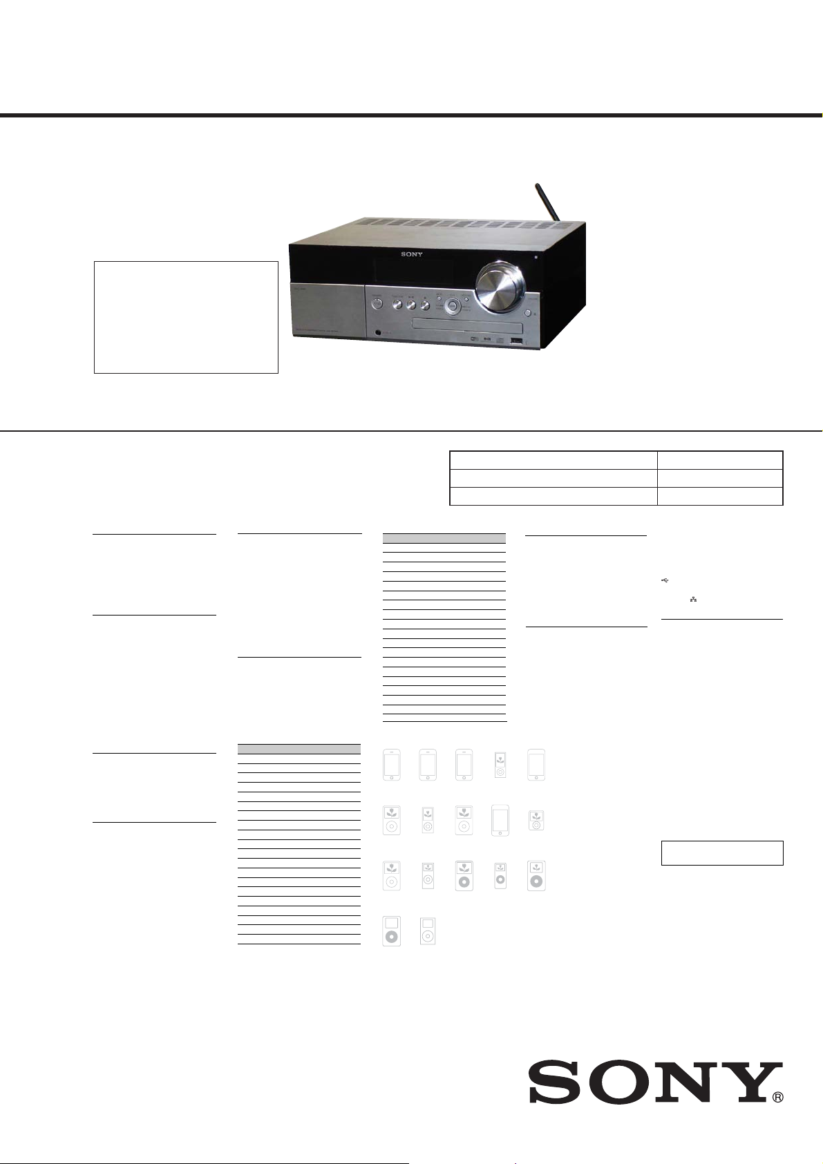
Photo: HCD-MX750Ni
• HCD-MX700Ni is the amplifi er, wireless LAN, CD player, tuner, iPod/iPhone and USB section in CMT-MX700Ni.
• HCD-MX750Ni is the amplifi er, wireless LAN, CD player, DAB/DAB+ tuner, iPod/iPhone and USB section in CMT-MX750Ni.
Model Name Using Similar Mechanism NEW
CD Mechanism Type CDM85CD-DVBU102
Optical Pick-up Block Name KHM-313CAA
SPECIFICATIONS
Main unit
AUDIO POWER SPECIFICATIONS
POWER OUTPUT AND TOTAL HARMONIC
DISTORTION:
(The United States model only)
With 6 ohm loads, both channels driven, from
120 Hz – 10,000 Hz; rated 50 watts per channel
minimum RMS power, with no more than 10%
total harmonic distortion from 250 milliwa tts to
rated output.
Amplifier section
European model:
DIN power output (rated):
40 watts + 40 watts (6 ohms at 1 kHz, DIN)
Continuous RMS power output (reference):
50 watts + 50 watts (6 ohms at 1 kHz, 10% THD)
Music power output (reference):
50 watts + 50 watts (6 ohms at 1 kHz, 10% THD)
Other models:
DIN power output (rated):
40 watts + 40 watts (6 ohms at 1 kHz, DIN)
Continuous RMS power output (reference):
50 watts + 50 watts (6 ohms at 1 kHz, 10% THD)
Wireless LAN section
Compatible standards:
IEEE 802.11 b/g (WEP 64 bit, WEP 128 bit,
WPA/WPA2-PSK (AES), WPA/WPA2-PSK
(TKIP))
Radio frequency:
2.4 GHz
CD player section
System:
Compact disc and digital audio system
Laser Diode Properties
Emission Duration: Continuous
Laser Output*: Less than 44.6μW
* This output is the value measurement at a distance of
200mm from the objective lens surface on the Optical
Pick-up Block with 7mm aperture.
Frequency response:
20 Hz – 20 kHz
Signal-to-noise ratio:
More than 90 dB
Dynamic range:
More than 90 dB
Tuner section
FM tuner section:
FM stereo, FM superheterodyne tuner
Tuning range:
North American model:
87.5 MHz – 108.0 MHz (100 kHz step)
Other models:
87.5 MHz – 108.0 MHz (50 kHz step)
Antenna:
FM lead antenna
Intermediate frequency:
10.7 MHz
DAB/DAB+ tuner section
(MX750Ni only):
FM stereo, DAB/FM superheterodyne tuner
Frequency range
Band-III:
174.928 (5A) MHz – 239.200 (13F) M Hz
Antenna:
DAB/FM lead antenna
DAB/DAB+ frequency table (Band-III)
Frequency Label
174.928 MHz 5A
176.640 MHz 5B
178.352 MHz 5C
180.064 MHz 5D
181.936 MHz 6A
183.648 MHz 6B
185.360 MHz 6C
187.072 MHz 6D
188.928 MHz 7A
190.640 MHz 7B
192.352 MHz 7C
194.064 MHz 7D
195.936 MHz 8A
197.648 MHz 8B
199.360 MHz 8C
201.072 MHz 8D
202.928 MHz 9A
204.640 MHz 9B
206.352 MHz 9C
208.064 MHz 9D
Frequency Label
209.936 MHz 10A
211.648 MHz 10B
213.360 MHz 10C
215.072 MHz 10D
216.928 MHz 11A
218.640 MHz 11B
220.352 MHz 11C
222.064 MHz 11D
223.936 MHz 12A
225.648 MHz 12B
227.360 MHz 12C
229.072 MHz 12D
230.784 MHz 13A
232.496 MHz 13B
234.208 MHz 13C
235.776 MHz 13D
237.488 MHz 13E
239.200 MHz 13F
iPod/iPhone section
Compatible iPod/iPhone models :
iPhone 3GS iPhone 3G iPhone iPod nano
iPod classic
iPod nano
120 GB 160 GB
4th generation
(2009)
(video)
iPod classic
iPod nano
80 GB
2nd generation
(aluminum)
iPod mini
iPod
eneration
4th
iPod classic
160 GB
(2007)
iPod
5th generation
(video)
5th generation
(video camera)
iPod touch
1st generation
iPod nano
1st generation
USB section
Supported bit rate:
MP3 (MPEG 1 Audio Layer-3): 32 kbps –
320 kbps, VBR
WMA: 48 kbps – 192 kbps, VBR
AAC: 48 kbps – 320 kbps
Sampling frequencies:
MP3 (MPEG 1 Audio Layer-3): 32/44.1/48 kHz
WMA: 44.1 kHz
AAC: 44.1 kHz
Inputs/Outputs
FM Antenna terminals:
75 ohms unbalanced
DAB/DAB+ Anten na terminal:
75 ohms, F female
AUDIO IN (stereo mini jack):
Sensitivity 700 mV, impedance 47 kilo hms
iPod touch
2nd generation
iPod nano
3rd generation
(video)
iPod
4th generation
(color display)
HCD-MX700Ni/MX750Ni
UK Model
Australian Model
SPEAKERS:
Accepts impedance of 6 ohms
iPod/iPhone Dock:
Output voltage: DC 5.0 V
The maximum output current: 500 mA
(USB) port:
Type A, maximum current 500mA
NETWORK port:
10BASE-T/100BASE-TX
General
Power requirements:
North American model:
AC 120V, 60Hz
Latin American models (except for Brazilian
models):
AC 110 V – 120 V or 220 V – 240 V, 50/60 Hz,
adjustable with voltage selector
Brazilian model:
AC 127 V or 220 V, 60 Hz, adjustable with voltage
selector
Taiwan model:
AC 120 V, 50/60 Hz
Other models:
AC 220 V – 240 V, 50/60 Hz
Power consumption:
43 watts
Dimensions (W/H/D) (excl. speakers):
Approx. 309 mm × 122 mm × 247 mm
1
(approx. 12
/4inch × 47/8 inch × 93/4 inch)
Mass (excl. speakers):
Approx. 3.0 kg
(approx. 6 lb 10 oz)
Design and specifications are subject to change
without notice.
s Standby power consumption: 0.5 W
s Halogenated flame retardants are not used in the
certain printed wiring boards.
E Model
HCD-MX700Ni
HCD-MX750Ni
9-889-945-03
2013B33-1
2013.02
©
COMPACT DISC RECEIVER
Sony Corporation
Published by Sony Techno Create Corporation
Page 2
HCD-MX700Ni/MX750Ni
• PARTY STREAMING and PARTY STREAMING logo are trademarks of Sony Corporation.
• VAIO and VAIO Media are registered trademarks of Sony Corporation.
• MPEG Layer-3 audio coding technology and patents licensed from Fraunhofer IIS and Thomson.
• Microsoft, Windows, Windows Vista, Windows 7™, Windows Media are trademarks or registered trademarks of Microsoft Corporation in the United States and/or other countries.
• iPod is a trademark of Apple Inc., registered in the U.S. and other countries.
• iPhone is a trademark of Apple Inc.
• “Made for iPod” and “Works with iPhone” means that an electronic accessory has been designed
to connect specifi cally to iPod or iPhone, respectively, and has been certifi ed by the developer to
meet Apple performance standards.
• Apple is not responsible for the operation of this device or its compliance with safety and regulatory standards.
• “
• DLNA®, the DLNA Logo and DLNA CERTIFIED™ are trademarks, service marks, or certifi ca-
• Wake-on-LAN is a trademark of International Business Machines Corporation in the United
• This product is protected by certain intellectual property rights of Microsoft Corporation. Use
• The system names and product names indicated in this manual are generally the trademarks or
• In this manual, Microsoft Windows XP Home Edition, Microsoft Windows XP Professional and
• In this manual, Microsoft Windows Vista Home Basic, Microsoft Windows Vista Home Pre-
• In this manual, Microsoft Windows 7 Starter, Microsoft Windows 7 Home Premium, Microsoft
• ™ and ® marks are omitted in this manual.
” is a mark of the Wi-Fi Alliance.
tion marks of the Digital Living Network Alliance.
States.
or distribution of such technology outside of this product is prohibited without a license from
Microsoft or an authorized Microsoft subsidiary.
registered trademarks of the manufacturer.
Microsoft Windows XP Media Center Edition are referred to as Windows XP.
mium, Microsoft Windows Vista Business and Microsoft Windows Vista Ultimate are referred
to as Windows Vista.
Windows 7 Professional, Microsoft Windows 7 Ultimate are referred to as Windows 7.
SAFETY CHECK-OUT
After correcting the original service problem, perform the following safety check before releasing the set to the customer:
Check the antenna terminals, metal trim, “metallized” knobs,
screws, and all other exposed metal parts for AC leakage.
Check leakage as described below.
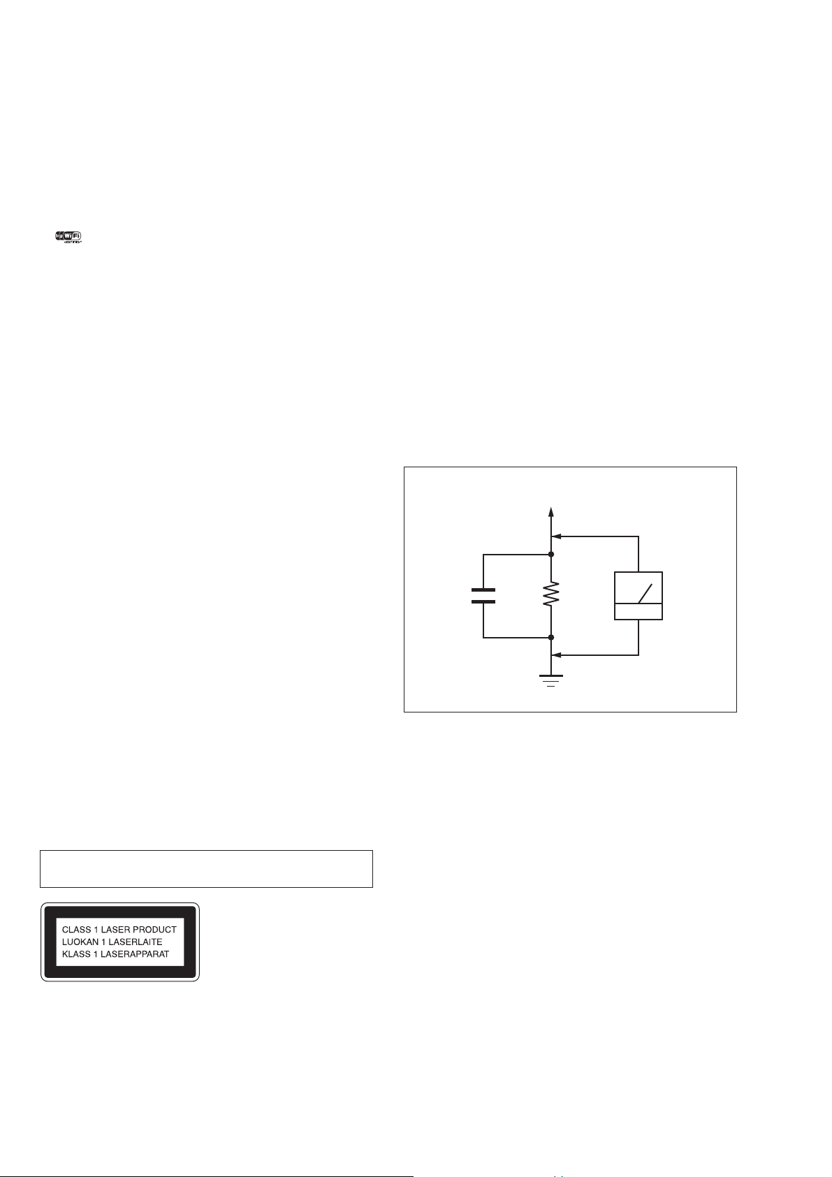
LEAKAGE TEST
The AC leakage from any exposed metal part to earth ground and
from all exposed metal parts to any exposed metal part having a
return to chassis, must not exceed 0.5 mA (500 microamperes.).
Leakage current can be measured by any one of three methods.
1. A commercial leakage tester, such as the Simpson 229 or RCA
WT-540A. Follow the manufacturers’ instructions to use these
instruments.
2. A battery-operated AC milliammeter. The Data Precision 245
digital multimeter is suitable for this job.
3. Measuring the voltage drop across a resistor by means of a
VOM or battery-operated AC voltmeter . The “limit” indication
is 0.75 V, so analog meters must have an accurate low-voltage
scale. The Simpson 250 and Sanwa SH-63Trd are examples
of a passive VOM that is suitable. Nearly all battery operated
digital multimeters that have a 2 V AC range are suitable. (See
Fig. A)
To Exposed Metal
Parts on Set
NOTES ON CHIP COMPONENT REPLACEMENT
• Never reuse a disconnected chip component.
• Notice that the minus side of a tantalum capacitor may be damaged by heat.
FLEXIBLE CIRCUIT BOARD REPAIRING
• Keep the temperature of soldering iron around 270 °C during
repairing.
• Do not touch the soldering iron on the same conductor of the
circuit board (within 3 times).
• Be careful not to apply force on the conductor when soldering
or unsoldering.
Laser component in this product is capable of emitting radiation
exceeding the limit for Class 1.
This appliance is classifi ed as
a CLASS 1 LASER product.
This marking is located on the
rear exterior.
SAFETY-RELATED COMPONENT WARNING!
COMPONENTS IDENTIFIED BY MARK 0 OR DOTTED LINE
WITH MARK 0 ON THE SCHEMATIC DIAGRAMS AND IN
THE PARTS LIST ARE CRITICAL TO SAFE OPERATION.
REPLACE THESE COMPONENTS WITH SONY PARTS
WHOSE PART NUMBERS APPEAR AS SHOWN IN THIS
MANUAL OR IN SUPPLEMENTS PUBLISHED BY SONY.
AC
1.5 kΩ0.15 μF
voltmeter
(0.75 V)
Earth Ground
Fig. A. Using an AC voltmeter to check AC leakage.
ATTENTION AU COMPOSANT AYANT RAPPORT
LES COMPOSANTS IDENTIFIÉS PAR UNE MARQUE 0 SUR
LES DIAGRAMMES SCHÉMATIQUES ET LA LISTE DES
PIÈCES SONT CRITIQUES POUR LA SÉCURITÉ DE FONCTIONNEMENT. NE REMPLACER CES COMPOSANTS QUE
PAR DES PIÈCES SONY DONT LES NUMÉROS SONT DONNÉS DANS CE MANUEL OU DANS LES SUPPLÉMENTS
PUBLIÉS PAR SONY.
À LA SÉCURITÉ!
2
Page 3

TABLE OF CONTENTS
1. SERVICING NOTES ............................................. 4
2. DISASSEMBLY
2-1. Disassembly Flow ........................................................... 9
2-2. Case ................................................................................. 9
2-3. NET Board Block ........................................................... 10
2-4. Front Panel Block ........................................................... 11
2-5. Knob (VOL) .................................................................... 12
2-6. SP Board ......................................................................... 12
2-7. MAIN Board ................................................................... 13
2-8. POWER Board ................................................................ 13
2-9. CD Block ........................................................................ 14
2-10. BD96U Board ................................................................. 15
2-11. Belt .................................................................................. 15
2-12. FFC Holder ..................................................................... 16
2-13. Optical Pick-up Block (KHM-313CAA) ........................ 16
3. TEST MODE ............................................................ 17
4. ELECTRICAL CHECK ......................................... 20
HCD-MX700Ni/MX750Ni
5. DIAGRAMS
5-1. Block Diagram - CD, USB Section - .............................. 21
5-2. Block Diagram
- TUNER, iPod/iPhone, AUDIO IN Section - ................ 22
5-3. Block Diagram
- NETWORK, OUTPUT, PANEL Section - ................... 23
5-4. Block Diagram - POWER SUPPLY Section - ................ 24
5-5. Printed Wiring Board - BD96U Board (Side A) - ........... 26
5-6. Printed Wiring Board - BD96U Board (Side B) - ........... 27
5-7. Schematic Diagram - BD96U Board (1/2) - ................... 28
5-8. Schematic Diagram - BD96U Board (2/2) - ................... 29
5-9. Printed Wiring Board - DAB Board (MX750Ni) - ......... 30
5-10. Schematic Diagram - DAB Board (MX750Ni) - ............ 31
5-11. Printed Wiring Board - MAIN Section (1/2) - ................ 32
5-12. Printed Wiring Boards - MAIN Section (2/2) - .............. 33
5-13. Schematic Diagram - MAIN Section (1/4) - ................... 34
5-14. Schematic Diagram - MAIN Section (2/4) - ................... 35
5-15. Schematic Diagram - MAIN Section (3/4) - ................... 36
5-16. Schematic Diagram - MAIN Section (4/4) - ................... 37
5-17. Printed Wiring Board - NET Board - .............................. 38
5-18. Schematic Diagram - NET Board - ................................. 39
5-19. Printed Wiring Boards - IP/JACK/SP/USB Boards - ..... 40
5-20. Schematic Diagram - IP/JACK/SP/USB Boards - .......... 41
5-21. Printed Wiring Boards - PANEL Section - ..................... 42
5-22. Schematic Diagram - PANEL Section - .......................... 43
5-23. Printed Wiring Board - POWER Board - ........................ 44
5-24. Schematic Diagram - POWER Board - .......................... 45
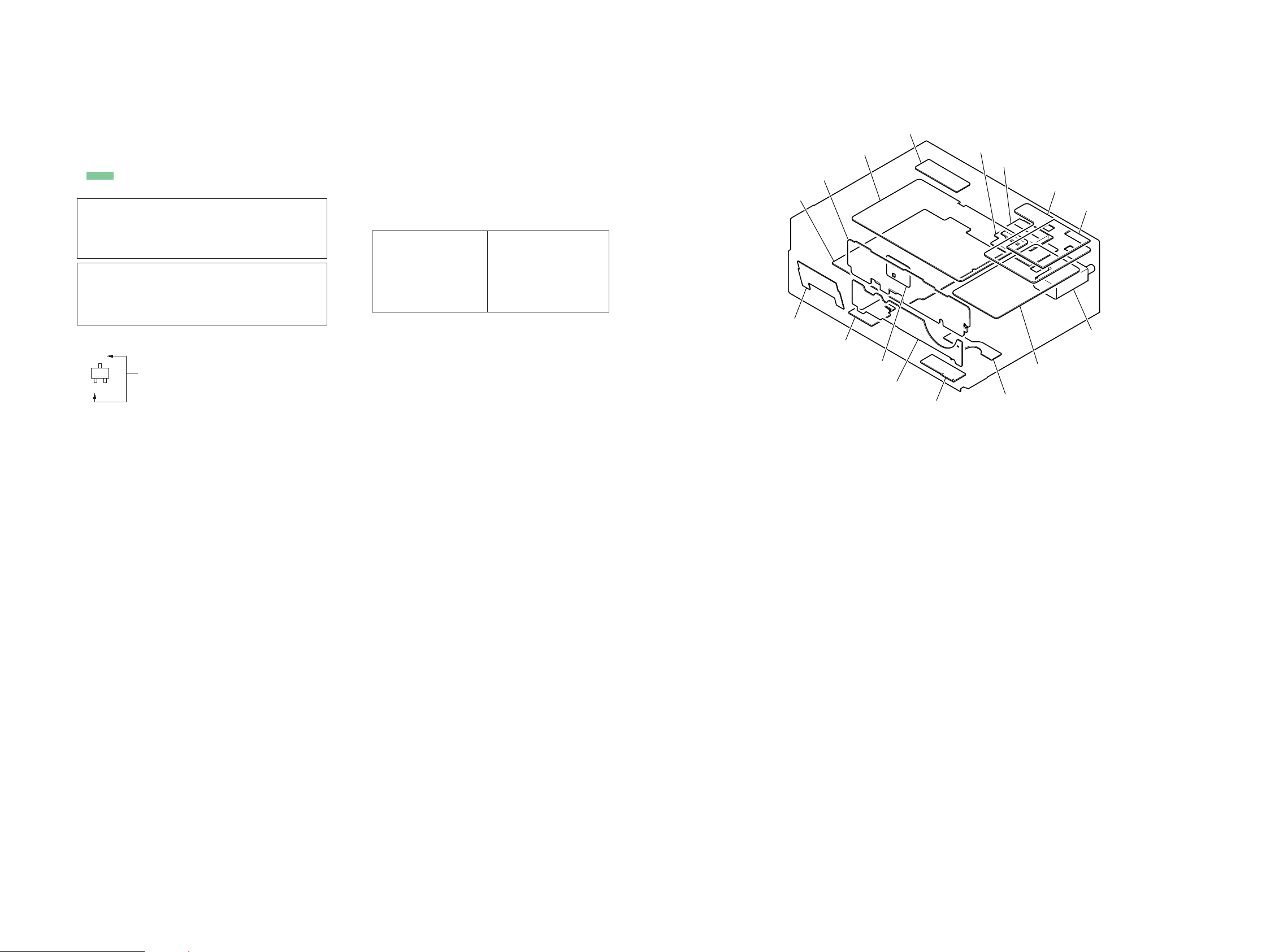
6. EXPLODED VIEWS
6-1. Case Section .................................................................... 58
6-2. Front Panel Section ......................................................... 59
6-3. iPod Dock Section .......................................................... 60
6-4. MAIN Board Section ...................................................... 61
6-5. Chassis Section ............................................................... 62
6-6. CD Mechanism Deck Section
(CDM85CD-DVBU102) ................................................ 63
7. ELECTRICAL PARTS LIST .............................. 64
3
Page 4
HCD-MX700Ni/MX750Ni
SECTION 1
SERVICING NOTES
NOTES ON HANDLING THE OPTICAL PICK-UP
BLOCK OR BASE UNIT
The laser diode in the optical pick-up block may suffer electrostatic break-down because of the potential difference generated by
the charged electrostatic load, etc. on clothing and the human body .
During repair, pay attention to electrostatic break-down and also
use the procedure in the printed matter which is included in the
repair parts.
The fl exible board is easily damaged and should be handled with
care.
NOTES ON LASER DIODE EMISSION CHECK
The laser beam on this model is concentrated so as to be focused
on the disc refl ective surface by the objective lens in the optical
pickup block. Therefore, when checking the laser diode emission,
observe from more than 30 cm away from the objective lens.
UNLEADED SOLDER
Boards requiring use of unleaded solder are printed with the leadfree mark (LF) indicating the solder contains no lead.
(Caution: Some printed circuit boards may not come printed with
the lead free mark due to their particular size)
: LEAD FREE MARK
Unleaded solder has the following characteristics.
• Unleaded solder melts at a temperature about 40 °C higher
than ordinary solder.
Ordinary soldering irons can be used but the iron tip has to be
applied to the solder joint for a slightly longer time.
Soldering irons using a temperature regulator should be set to
about 350 °C.
Caution: The printed pattern (copper foil) may peel away if
the heated tip is applied for too long, so be careful!
• Strong viscosity
Unleaded solder is more viscous (sticky, less prone to fl ow)
than ordinary solder so use caution not to let solder bridges
occur such as on IC pins, etc.
• Usable with ordinary solder
It is best to use only unleaded solder but unleaded solder may
also be added to ordinary solder.
NOTE OF REPLACING THE WIRELESS LAN MODULE
(MOD1)
When replacing the wireless LAN module (MOD1), MAC address
is changed. Print the following explanation, cut it, and hand over it
to the customer with the set, when returning the set that the repair
is completed to the customer.
MAC address of the main unit has been changed by this repair.
When using the MAC address fi ltering function of connection destina-
tion access point equipment, set it again..
CHECKING METHOD OF NETWORK OPERATION
It is necessary to check the network operation, when replacing the
wireless LAN module (MOD1). Check the operation of wireless
and wired LAN, according to the following method.
1. Checking Method of Wireless LAN Operation
Check that access point is recognized surely.
Necessary Equipment:
Wireless access point with router function (AP)
Procedure:
1. Press the [FUNCTION] button to select the Home Network
function.
2. Press the [ + v]/[V –] buttons to select “Network,” then
press the [ENTER] button.
3. Press the [ + v]/[V –] buttons to select “Settings,” then
press the [ENTER] button.
4. Press the [ + v]/[V –] buttons to select “Wireless LAN
Settings,” then press the [ENTER] button.
5. Press the [ + v]/[V –] buttons to select “Access Point
Scan,,” then press the [ENTER] button.
6. The system starts searching for access points, and displays a
list of up to 20 available network name (SSID).
7. Check that access point (SSID) is displayed on the searching
result.
Note: Refer to the instruction manual about details of the setting method.
2. Checking method of wired LAN operation
Check that access point is recognized surely.
RELEASING THE DISC TRAY LOCK
The disc tray lock function for the antitheft of an demonstration
disc in the store is equipped.
Releasing Procedure:
1. Press the [
2. Press two buttons of [x] and [Z] for 5 seconds.
3. The message “UNLOCKED” is displayed on the liquid crystal
element and the disc tray is unlocked.
Note: When “LOCKED”is displayed, the disc tray lock is not released by
turning power on/off with the [
NOTE OF REPLACING THE MS-203 BOARD
When the MS-203 board is damaged, exchange the entire
CDM85 (CD) ASSY.
NOTE OF REPLACING THE CN1003 ON THE NET
BOARD
CN1003 on the NET board cannot exchange with single. When
these parts are damaged, exchange the entire mounted board.
] button to turn the power on.
?/1
?/1
] button.
Procedure:
1. Connect the main unit to the router or the hub, etc. with the
LAN cable.
2. Press the [FUNCTION] button to select the Home Network
function.
3. Press the [ + v]/[V –] buttons to select “Network,” then
press the [ENTER] button.
4. Press the [ + v]/[V –] buttons to select “Settings,” then
press the [ENTER] button.
5. Press the [ + v]/[V –] buttons to select “Wired LAN Settings,” then press the [ENTER] button.
Note: If “Change Setting?” appears, select “OK,” then press the [ENTER]
button.
6. On the IP setting, press the [ + v]/[V –] buttons to select
“Auto,” then press the [ENTER] button.
7. On the proxy setting, press the [
select “Do Not Use,” then press the [ENTER] button.
8. Press the [ + v]/[V –] buttons to select “OK,” then press
the [ENTER] button.
9. Perform the server settings.
10. Press the [OPTIONS] buttons to select “Network,” then press
the [ENTER] button.
11. Press the [OPTIONS] buttons to select “Information,” then
press the [ENTER] button.
12. Check that IP address can be acquired.
Note: Refer to the instruction manual about details of the setting method.
+ v]/[V –] buttons to
4
Page 5
MODEL IDENTIFICATION
– Back Panel –
Model Part No.
HCD-MX700Ni: AEP model
HCD-MX700Ni: US model
HCD-MX700Ni: Canadian model
HCD-MX700Ni: Taiwan model
HCD-MX700Ni: Latin American model
HCD-MX700Ni: Brazilian model
HCD-MX750Ni: AEP, UK models
HCD-MX750Ni: Australian model
PART No.
HCD-MX700Ni/MX750Ni
4-189-496-0[]
4-189-496-1[]
4-189-496-2[]
4-189-496-4[]
4-189-496-5[]
4-189-496-6[]
4-189-496-7[]
4-189-496-8[]
CAPACITOR ELECTRICAL DISCHARGE PROCESSING
When checking the board, the electrical discharge is necessary for the electric shock prevention.
Connect the resistors referring to the fi gure below.
• POWER board (C10) (AEP and UK models)
Both ends of respective capacitors.
– POWER Board (Conductor Side) –
C10
800 :/2 W
• POWER board (C11, C12) (Except AEP and UK models)
Both ends of respective capacitors.
– POWER Board (Conductor Side) –
C12
C11
800 :/2 W
800 :/2 W
5
Page 6
HCD-MX700Ni/MX750Ni
HOW TO OPEN THE TRAY WHEN POWER SWITCH TURN OFF
2
bottom side
1 Insert the hard metal fittings of L character type in the
hole of the chassis, and push the lever in the direction
of the arrow.
MAIN BOARD (COMPONENT SIDE), BD96U BOARD (COMPONENT SIDE) AND SP BOARD SERVICE POSITION
SP board
MAIN board
BD96U board
6
Page 7
NET BOARD SERVICE POSITION
MAIN board
HCD-MX700Ni/MX750Ni
NET board
insulating sheet
LCD, KEY, JACK AND USB BOARDS SERVICE POSITION
WIRELESS LAN MODULE (MOD1)
JACK board
LCD board
JUNCTION board
KEY board
USB board
7
Page 8
HCD-MX700Ni/MX750Ni
MAIN BOARD (CONDUCTOR SIDE) AND BD96U BOARD (CONDUCTOR SIDE) SERVICE POSITION
MAIN board
(conductor side)
BD96U board
(conductor side)
POWER board
DAB board
(MX750Ni only)
POWER BOARD SERVICE POSITION
Note: Please disassemble each board from the chassis.
POWER board
MAIN board
LCD board
8
Page 9
DISASSEMBLY
• This set can be disassembled in the order shown below.
2-1. DISASSEMBLY FLOW
SET
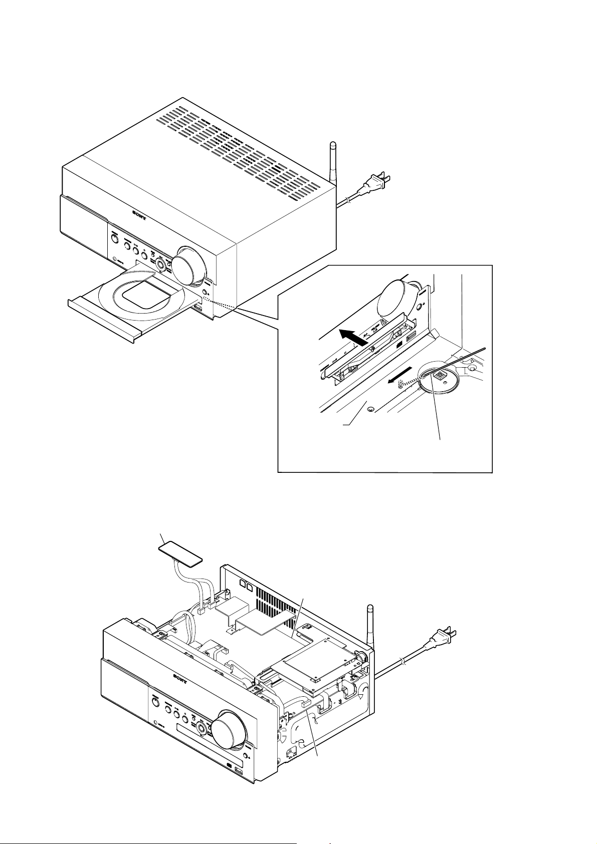
2-2. CASE
(Page 9)
HCD-MX700Ni/MX50Ni
SECTION 2
2-4. FRONT PANEL BLOCK
(Page 11)
2-5. KNOB (VOL)
(Page 12)
Note: Follow the disassembly procedure in the numerical order given.
2-3. NET BOARD BLOCK
(Page10)
2-7. MAIN BOARD
(Page 13)
2-9. CD BLOCK
(Page 14)
2-10. BD96U BOARD
(Page 15)
2-12. FFC HOLDER
(Page 16)
2-13. OPTICAL PICK-UP BLOCK
(KHM-313CAA)
(Page 16)
2-6. SP BOARD
(Page 12)
2-8. POWER BOARD
(Page 13)
2-11. BELT
(Page 15)
2-2. CASE
1 two screws
(BV/RING)
– Bottom view –
5 case
3
2 three screws
(BV/RING)
4
3
9
Page 10
HCD-MX700Ni/MX750Ni
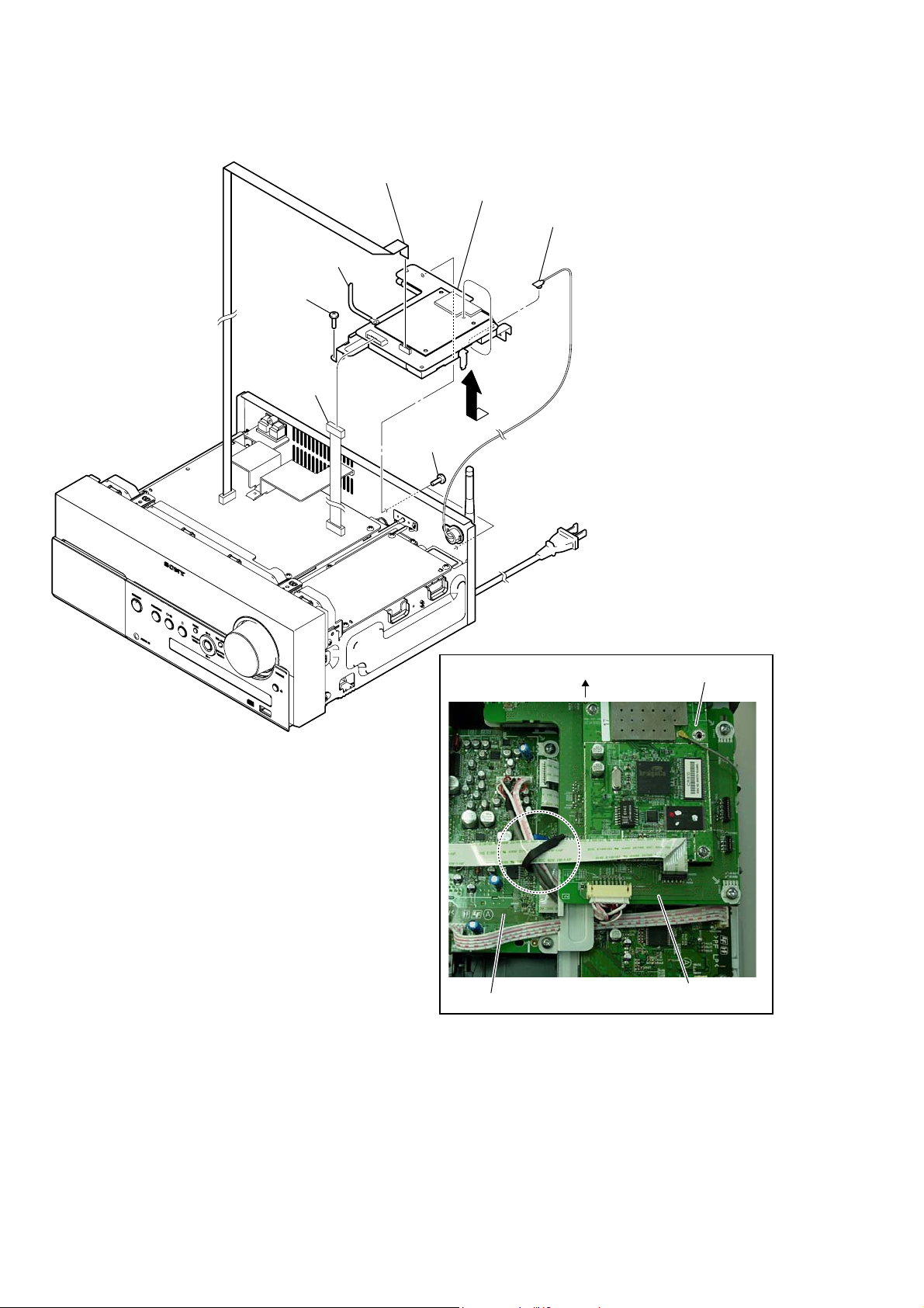
2-3. NET BOARD BLOCK
5 screw
(BV3)
2 Lift up the
coating clip.
3 flexible flat cable (11 core)
(CN1005)
7 NET board block
1 antenna cable
Note:
surely connected when you install
the NET board block.
Please confirm the antenna cable is
4 connector
(CN1004)
5 two screws
(BV3)
:LUHVHWWLQJ
6
rear
WIRELESS LAN MODULE
(MOD1)
10
MAIN board
NET board
Page 11
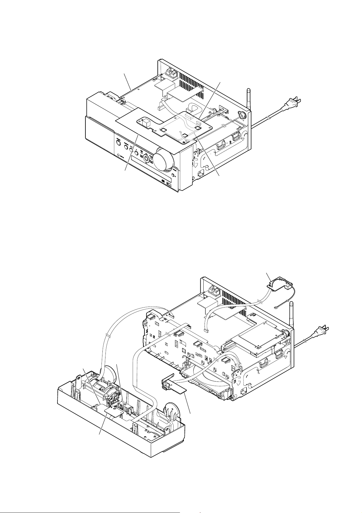
2-4. FRONT PANEL BLOCK
5 Lift up the coating clip.
8 flexible flat cable
qs two screws
(BV3)
qg two claws
(15 core) (CN403)
6 flexible flat cable
(13 core) (CN409)
7 ferrite core
9 connector
(CN402)
qd screw (BV3)
HCD-MX700Ni/MX50Ni
lead wire (from HP board)
qf
qh front panel block
3 two claws
4 panel (CD) block
qg two claws
qs three screws
(BV3)
2 Draw out
the tray.
0 connector
(CN402)
qa screw
(BV3)
bottom side
1 Insert the hard metal fittings of L character type in the
hole of the chassis, and push the lever in the direction
of the arrow.
11
Page 12
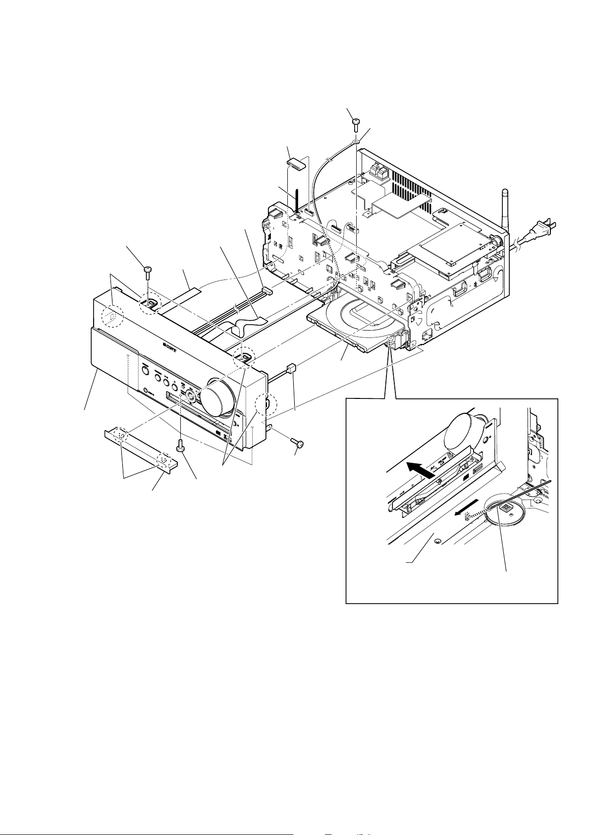
HCD-MX700Ni/MX750Ni
2-5. KNOB (VOL)
knob (VOL)
2
2-6. SP BOARD
2 connector (CN703)
1 connector (CN702)
hole
LCD board
Push the knob (VOL) by flat-head screwdriver.
1
– Front panel block inside view –
front panel block
4
5 SP board
3 screw (BV3)
12
Page 13
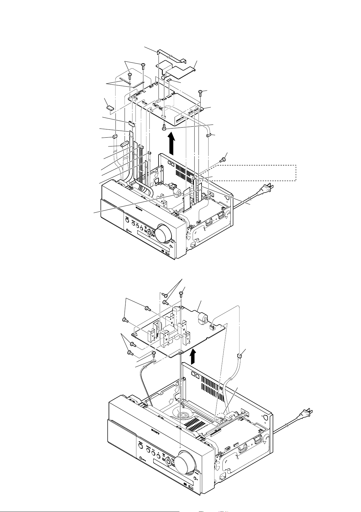
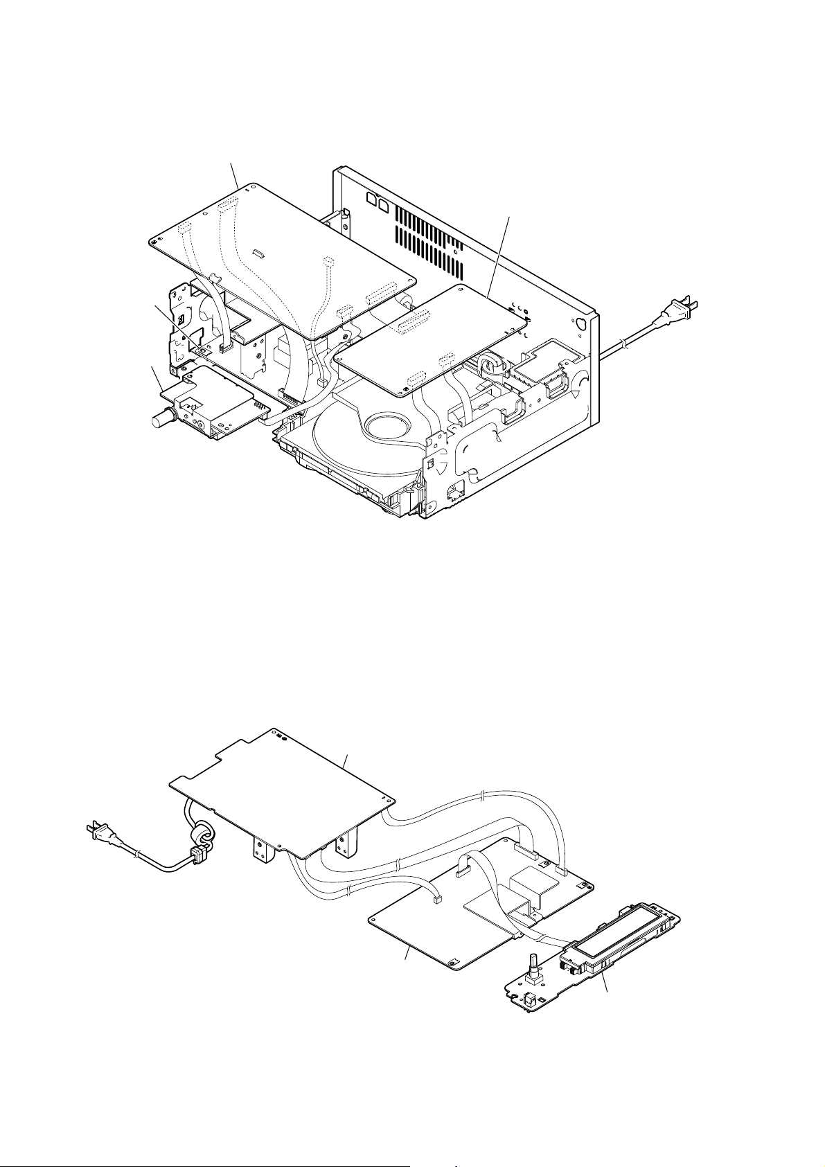
2-7. MAIN BOARD
ql flexible flat cable (11 core)
(CN411)
qd two screws (BV3)
HCD-MX700Ni/MX50Ni
qj heatsink (AMP)
qf two coating clips
w; cushion (ferrite)
2 ferrite core
1 flexible flat cable
(13 core) (CN409)
3 connector (CN704)
4 connector (CN412)
5 flexible flat cable
(13 core) (CN404)
6 connector (CN402)
7 connector (CN417)
8 flexible flat cable
(5 core) (CN410)
9 flexible flat cable
(27 core) (CN415)
qk radiation sheet
qd three screws (BV3)
wa MAIN board
qh two screws (BV3)
qs connector (CN401)
qg
qd screw (BV3)
(MX750Ni)
qa flexible flat cable (9 core) (CN407)
0 flexible flat cable (9 core) (CN405)
(Except AEP, UK)/
flexible flat cable (11 core) (CN406)
(AEP, UK)
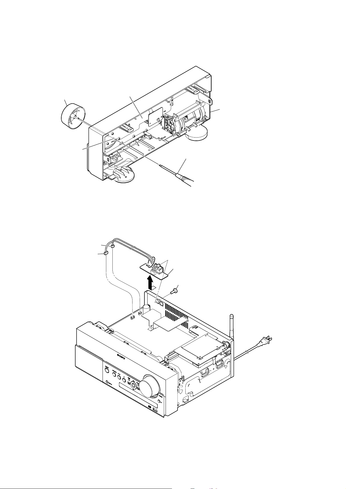
2-8. POWER BOARD
6 two screws (BV3)
6 two screws (BV3)
lead wire (from HP board)
3
2 screw (BV3)
6 two screws (BV3)
2 two screws (BV3)
7 POWER board
5
1 power cord connector
(CN1)
4 claw
13
Page 14
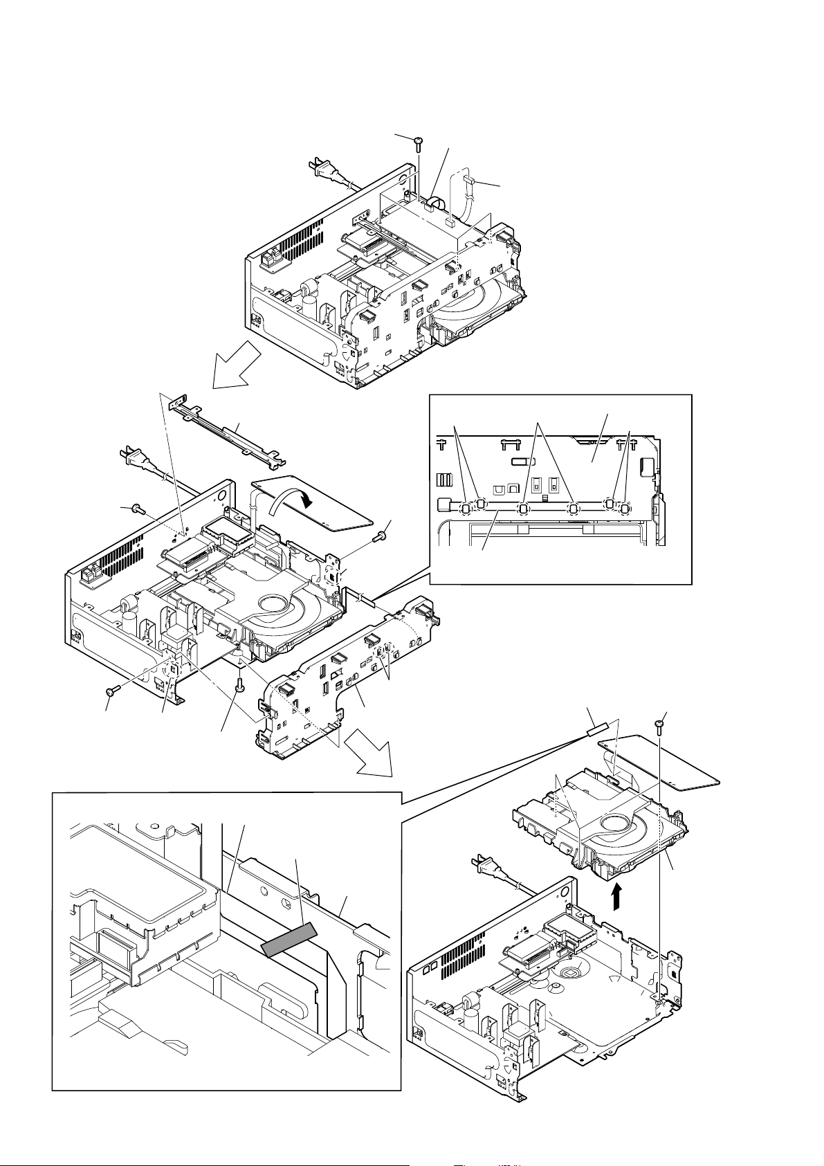
HCD-MX700Ni/MX750Ni
2-9. CD BLOCK
4 screw (BV3)
2 four screws (BV3)
6 bracket (center)
3
8 screw
(BV3)
Note 1: Do not remove this connector (CN201) at this point.
It is necessary to process electrostatic measures of
optical pick-up.
1 connector (CN301)
7 two claws
7 two claws
bracket (front)
7 two claws
8 screw (BV3)
9 claw
8 screw (BV3)
flexible flat cable 24P
filament tape
9 claw
0 bracket (front)
guard board
flexible flat cable (5 core)
5 two claws
– Front side view –
qa filament tape
qs three screws
(BV3)
qf CD block
qd
Note 2: When you install CD block, fix the flexible flat cable 24P with
the filament tape firmly as shown in figure.
14
Page 15
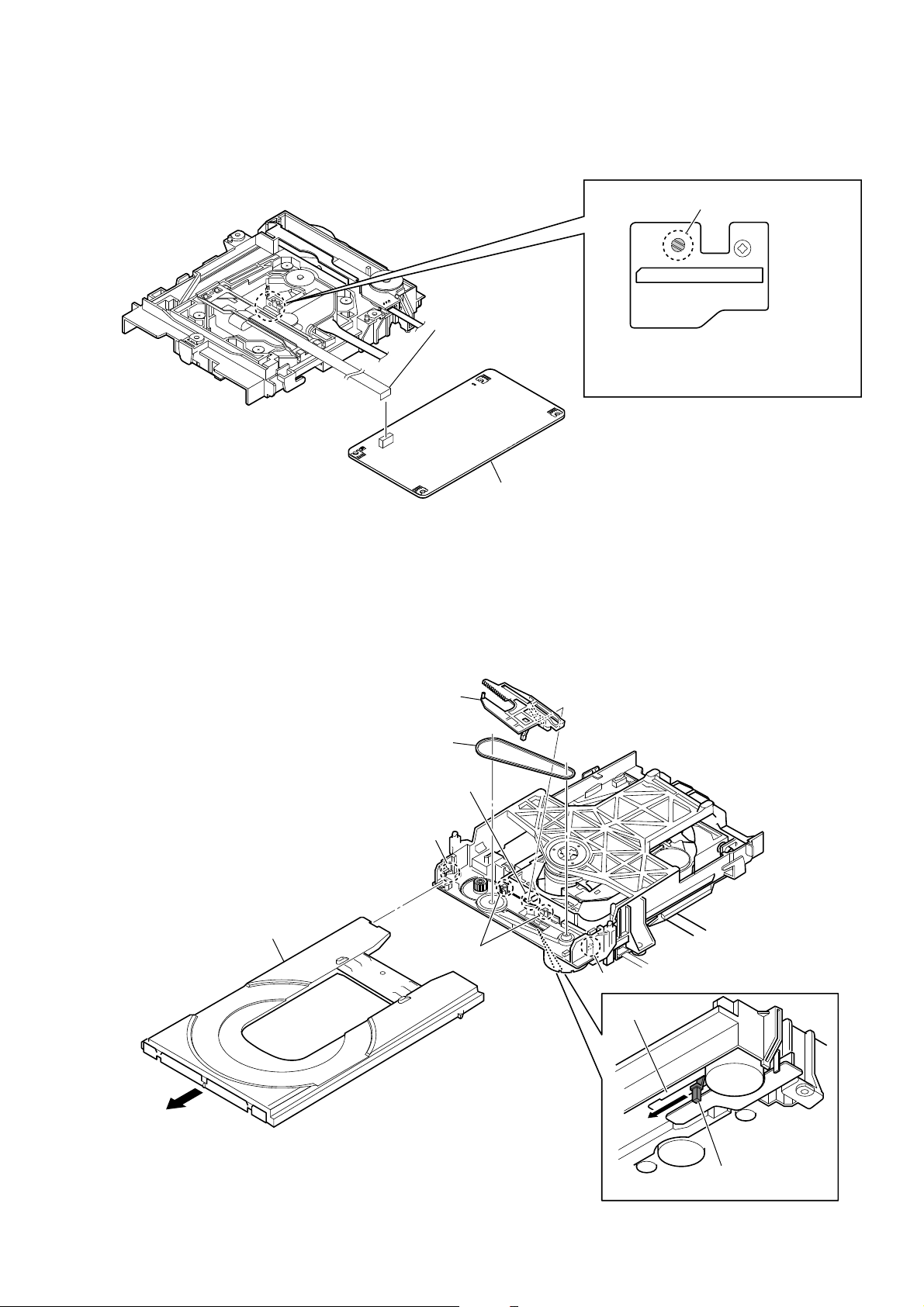
2-10. BD96U BOARD
Note 1: When disconnection the wire (fl at type) (24 core) of optical pick-up block, solder the short-land.
flexible flat cable 24P
2
(CN201)
Note 2: When assembling the optical pick-up block,
remove the solder of short-land after
connecting the flexible flat cable 24P.
– CD mechanism deck block bottom view –
HCD-MX700Ni/MX50Ni
Solder the short-land.
1
2-11. BELT
3 BD96U board
7 chuck cam
8 belt
6 shaft
3 claw
4 tray
5 two hooks
2
3 claw
bottom side
1 Push the lever in the
direction of the arrow.
15
Page 16
HCD-MX700Ni/MX750Ni
2-12. FFC HOLDER
3 FFC holder
Note: Remove the FFC holder from the
original set and install it again.
1 two claws
2 two claws
– CD mechanism deck block bottom view –
2-13. OPTICAL PICK-UP BLOCK (KHM-313CAA)
+ow to bend the flexible flat cable 24P
two screws
optical pick-up block
6
(KHM-313CAA)
two screws
1
(PTPWH M2.6)
insulator
3
connector
5
insulator
3
1
(PTPWH M2.6)
insulator
3
1 two claws
to BD96U board
(CN201)
flexible flat cable 24P
4
insulator
3
40 mm
The upper side
is contact side.
The lower side
is contact side.
40 mm
to optical pick-up block
(KHM-313CAA)
50 mm
16
– CD mechanism deck block bottom view –
mechanism deck
2
(CDM85 (CD))
Page 17

SECTION 3
TEST MODE
HCD-MX700Ni/MX750Ni
COLD RESET
The cold reset clears all data including preset data stored in the
memory to initial conditions. Execute this mode when returning
the set to the customer.
Procedure:
1. In the standby status, press the [?/1] button to turn the power
on.
2. Press two buttons of [ENTER] and [
3. When “RESET” appears, the set enters.
AUTO STANDBY MODE
This mode is used to change the automatic standby function.
With this function, the system enters standby mode automatically
in about 30 minutes when there is no operation or audio signal
output. By default, the automatic standby function is turned on.
Procedure:
1. Press the [
2. Press the [
3. The message “AUTO STANDBY” is displayed on the liquid
crystal element and the automatic standby OFF mode is set.
4. T o turn this function on, press the [
onds.
The message “AUTO STANDBY” is displayed on the liquid
crystal element and the automatic standby ON mode is set.
COMMON TEST MODE
This mode is used to check operations of amplifi er.
Procedure:
1. Press the [
2. Press two buttons of [ENTER] and [FUNCTION] simultaneously.
3. When the COMMON test mode is activated, “AUDIO IN” is
displayed on the liquid crystal element and “c PLA Y SLEEP”
blink on the liquid crystal element.
4. Each time [EQ] button on the remote commander is pressed,
the display changes starting “TONE MAX”, “TONE MIN”
and “TONE FLAT” this order.
5. Turn the [VOLUME] knob counterclockwise, “VOLUME
MIN” is displayed on the liquid crystal element. Turn the
[VOLUME] knob clockwise, “VOLUME MAX” is displayed
on the liquid crystal element.
Releasing method:
Press the [
PANEL TEST MODE
This mode is used to check the liquid crystal element, LED, model,
destination, software version and key.
Procedure:
1. Press the [?/1] button to turn the power on.
2. Press two buttons of [ENTER] and [x] simultaneously.
3. All segments on the liquid crystal element, [STANDBY] LED
light up.
4. Press the [ENTER] button, the model and destination are displayed on the liquid crystal element.
5. Press the [ENTER] button again, MC version is displayed on
the liquid crystal element.
6. Each time [ENTER] button is pressed, the display changes
starting from MC version, GC version, USBL version , USBM
version, NWA version, NWD version, NWM version, IPL version, CD version, CDD version, CDMA version, CDMB version, BDA version, BDB version, ST version, TA version and
TM version this order, and returns to the MC version display.
7. When [
year, month and day of the software creation is displayed.
When [
MC version display.
] button to turn the power on.
?/1
] button for 2 seconds.
?/1
] button to turn the power on.
?/1
] button to turn off the system.
?/1
] button is pressed while the MC version is displayed,
x
] button is pressed again, the display returns to the
x
] simultaneously.
?/1
] button again for 2 sec-
?/1
8. Press the [OPTIONS] button, the key test mode is activated
and “K 0 V0” is displayed on the liquid crystal element.
9. Each time a button is pressed, “K” value increases. However,
once a button is pressed, it is no longer taken into account.
All keys are pressed, display becomes “K11” .
10. “V” value increases 2, 4, 6 ... if turn the [VOLUME] knob
clockwise, or it decreases 8, 6, 4 ... if turn the knob counterclockwise.
Releasing method:
Press two buttons of [ENTER] and [
nect the power cord.
CD SHIP MODE
This mode moves the optical pick-up to the position durable to
vibration. Use this mode when returning the set to the customer
after repair.
Procedure:
1. Press the [?/1] button to turn the power on.
2. Press the [FUNCTION] button to select “CD”.
3. Press two buttons of [OPTIONS] and [?/1] simultaneously.
4. After blink “STANDBY”, “LOCK” is displayed, disconnect
the AC plug.
CD SHIP MODE & MEMORY CLEAR
This mode is used to perform CD ship mode and cold reset simultaneously.
Procedure:
1. Press the [
2. Press three buttons of [
3. After blink “STANDBY”, “LOCK” is displayed disconnect
the AC plug.
DISC TRAY LOCK MODE
This mode is used to unable to take sample disc out of disc tray in
the shop.
Procedure:
1. Press the [?/1] button to turn the power on.
2. Press the [Z] button to open the disc tray and set the CD disc.
3. Press the [Z] button to close the disc tray.
4. Press two buttons of [x] and [Z] for 5 seconds.
5. The message “LOCKED” is displayed on the liquid crystal element and the disc tray is locked. (Even if pressing the [Z] button, the message “LOCKED” is displayed on the liquid crystal
element and the disc tray is locked)
Releasing method:
1. Press two buttons of [
2. The message “UNLOCKED” is displayed on the liquid crystal
element and the disc tray is unlocked.
CD POWER MANAGE
This mode is used to changed over CD power on/off for decreasing
of reception noise in the tuner mode.
Procedure:
1. Press the [?/1] button to turn the power on.
2. Press the [FUNCTION] button to select “CD”.
3. Press the [?/1] button again to turn the power off.
4. Press two buttons of [ + v] and [?/1] simultaneously.
5. The message “CD POWER ON” or “CD POWER OFF” is displayed on the liquid crystal element, and CD power on/off is
changed over in the tuner mode.
] button to turn the power on.
?/1
] and [BACK] simultaneously.
x
] and [Z] for 5 seconds.
x
] simultaneously, or discon-
x
17
Page 18
HCD-MX700Ni/MX750Ni
CD SERVICE MODE
This mode can run the CD sled motor freely. Use this mode, for
instance, when cleaning the optical pick-up.
Procedure:
1. Press the [?/1] button to turn the power on.
2. Press the [FUNCTION] button to select “CD”.
3. Press three buttons of [x] and [ + v] simultaneously, the
message “SER VICE MODE” is displayed on the liquid crystal
element.
4. Press the [
l m
up to inside track and the message “SLED IN” is displayed
on the liquid crystal element, or press the [
+] button to outside track and the message “SLED OUT” is
displayed on the liquid crystal element.
5. Press the [u] button, “LD ON” or “LD OFF” is displayed on
the liquid crystal element. Each time [u] button is pressed,
laser diode on/off is changed over.
Releasing method:
Press the [
] button to turn off the system.
?/1
CD SERVO TEST MODE
This mode can check the servo system operations of the optical
pick-up system (= optical unit + BD96U board).
Note 1: Do not enter the [CD SERVO TEST MODE] while any other test
mode is in progress.
Note 2: Do not enter any other test mode while the [CD SERVO TEST
MODE] is in progress.
Note 3: In RAM Read, “SBADrough”, “SBBTrough”, “DT-GI rough”,
“SBAD fi ne”, “SBBT fi ne”, “DT-GI fi ne”, “DSPcomcnt”, and
“DECcomcnt” are displayed but are not used in the service.
How to Enter the CD Servo Test Mode
Procedure:
1. Press the [
?/1
2. Press the [FUNCTION] button to select CD function.
3. Press three buttons of [x], and [V –] simultaneously.
4. It enters the CD servo test mode and displays “bdt S CURVE”.
How to Exit from the CD Servo Test Mode
Procedure:
1. To release this mode, press the [
Key Operation:
[ + v], [V –]:
Use these keys to move between the seven modes contained in the
CD Servo Test Mode, that are the S-Curve Mode, the RAM Read
Mode, the RAM Write Mode, the Command Out Mode, the Error
Rate Mode the LOG Initialize Mode and the LOG Read Mode as
described below. Also, use these keys to move between the menus
within the respective seven modes. When [ + v] is pressed, the
screen advances to the next menu or to the next mode. When [
–] is pressed, the screen returns back to the previous menu or
to the previous mode. Use these keys also to increase or decrease
the numeric value when changing the numeric value. Pressing [
+ v] increases the value and pressing [V –] decreases the value.
[ENTER], [
]:
x
Use these keys to move between the different layers of the hierarchy of the CD Servo Test Mode shown below. Press [ENTER]
to move down to the lower layer, and press [
higher layer.
[
M L
TUNE +], [
Use these keys to move the cursor to the right digit or to the left
digit in the six-digit number, when changing the numeric value.
Press [
M L
press [
l m
TUNE –] button to move the optical pick-
M L
TUNE
] button to turn the power on.
] button.
?/1
] to move up to the
x
l m
TUNE –]:
TUNE +] to move the cursor to the right, and
TUNE –] to return the cursor to the left.
V
[
]:
u
Use this key to execute Command Out in the Command Out Mode.
CD Servo Test Mode Tree:
S Curve Mode LD ON
(bdt S CURVE) (LD ON)
RAM Read Mode
(bdtRAM READ) (DiscType) (AL: 0000, RW: 0001)
Gain Index value indication
(GainIndx) (0001)
RFO GAIN value indication
(RFO_GAIN) (0008)
FEO GAIN value indication
(FEO_GAIN) (0005)
SBAD GAIN value indication
(SBAD_GAIN) (0008)
TEO GAIN value indication
(TEO_GAIN) (0008)
Disc Size value indication
(DiscSize) (0000: Non disc, 0001: 8cm,
0002: 12cm)
(OpAbrkErr) (0000)
SBBT Data value indication
(SBBT Data) (0053)
TE Peak value indication
(TE P-P) (0097)
FEOOCD value indication
(FEOOCD) (00C0)
The following items are not used (Note 3)
RAM Write Mode
(bdtRAM WRITE) (00 SPG_Mask) (Non mask:00, Mask:01)
Fix RF Gain value edit
(00 FixRFgain) (Non Fix:00, AL Fix:01, RW Fix:02)
TMAX ON value edit
(00 tmaxon)
Driver Mute OFF value edit
(00 d_muteoff) (Normal:00, Forced OFF:01)
Command Out Mode
(bdt COMOUT) (COMOUT6X) (000000) (ok)
READ2X value edit command out
(READ2X) (60) (50)
REG READ value edit command out
(REG_READ) (00) (0000)
FEBC? command out
(FEBC?) (00)
FGADD? command out
(FGADD?) (FA)
TEBC? command out
(TEBC?) (02)
TGADD? command out
(TGADD?) (0D)
RFGC? command out
(RFGC?) (3F)
FEOF? command out
(FEOF?) (0000)
TEOF? command out
(TEOF?) (FFC0)
TEIOCD1? command out
(TEIOCD1?) (FEC0)
TEIOCD2? command out
(TEIOCD2?) (FEC0)
TEIOCD3? command out
(TEIOCD3?) (0080)
TEOOCD? command out
(TEOOCD?) (FB80)
FEOOCD? command out
(FEOOCD?) (00C0)
MONITOR value edit command out
(MONITOR) (570A00) (ok)
Error Rate Mode Error rate indication
(bdt ERR RATE) (0000000000)
LOG Read Mode value indication
(bdtLOG READ) (XX: YYYYYY: ZZZZ)
XX: LOG Number
YYYYYY: Communication LOG
ZZZZ: LOG Number
LOG Initialize Mode Initializetion Initialization execution
(bdtLOG INIT) confirmation (INIT done)
indication
(INIT sure?)
Higher layer Lower layer of menu hierarchy
Disc Type value indication
Op ABRAKE Error
SPG Mask value edit
COMOUT6X value edit command out
value indication
18
Page 19
HCD-MX700Ni/MX750Ni
CD ERROR CODE
The past errors of the CD mechanism (CDM) are displayed as the
CDM Errors, and those of the optical pick-up system (= optical
unit + BD96U board) are displayed as the BD Errors as shown
below.
Procedure:
1. Press the [
2. Press the [FUNCTION] button to select CD function.
3. Press three buttons of [OPTIONS] and [
4. BD and CDM error counts are displayed on the fl uoresent in-
dicator tube as shown below.
] button to turn the power on.
?/1
] simultaneously.
u
Em**Ed** X
Mode-in count
BD error count
CDM error count
5. Press the [
6. Then, the CDM error code is displayed as “M0xxxxxxxx” (x
means hexadecimal number) on the liquid crystal element as
shown below.
7. Every pressing of the [
increments the number after “M” starting from “M0” up to
“M9”, and then returns to “M0”. Every pressing of the [
m
TUNE –] button in this mode decrements the number after
“M”. The smaller the error code number is, the newer the error
content is.
Press the [
8. When the [
is displayed as “D0xxxxxxxx” (x means hexadecimal number)
on the fl uoresent indicator tube as shown below. In the same
way as the CDM error code, use of the [
and the [
ing of the error history.
Press the [
Releasing method:
Press the [?/1] button to turn off the system.
Contents of “CDM Errors”
Error display example
M 0 FF 11 42 00
1 2 3 4 5
1 It indicates the error history number
0 to 9: The error code number 0 indicates the newest error.
2 It indicates whether the CDM error occurs in the normal opera-
tions or during the initialization operation.
FF : The error has occurred in the normal opera-
Other than FF : The error has occurred during the initialization
3 It indicates the processing during which the trouble has oc-
curred.
01: The disc EJECT processing is in progress.
02: The disc INSERTION-WAITING processing is in prog-
ress.
03: Processing of the disc INSERTION-REQUEST for the up-
per CD tray is in progress.
04: Processing of the disc EJECTION-REQUEST for the up-
per CD tray is in progress.
05: The disc pulling-in operation is in progress.
06: The disc chucking processing is in progress.
07: The disc re-chucking processing is in progress.
+ v] button.
M L
–] button to return to the previous display.
V
+ v] button is pressed then, the BD error code
l m
TUNE –] buttons in this mode enables trac-
–] button to return to the previous display.
V
tions.
operation.
TUNE +] button in this mode
M L
l
TUNE +]
08: The disc chucking-release completion operation is in prog-
ress.
4 It indicates the operation during which the trouble has oc-
curred.
00 : Waiting for the operation.
10 to 13 : The disc EJECT operation is in progress.
20 : The disc pulling-in operation is in progress.
30 : The disc chucking-release operation is in progress.
40 to 43 : The disc EJECT operation due to error is in prog-
ress.
5 Reserve
00: Fix
Contents of “BD Errors”
Error display example
D
0 02 09
1 2 3 4 5
1 It indicates the error history number
0 to 9: The error code number 0 indicates the newest error.
2 It indicates the error content
01: The focus servo cannot lock-in.
02: GFS is no good (NG).
03: The startup time exceeds the specifi ed period of time (time
over)
04: The focus servo is unlocked continuously.
05: Q code cannot be obtained within the specifi ed period of
time.
06: The tracking servo cannot lock-in.
07: Blank disc
3 It indicates the on-going processing of optical pick-up system
(= optical unit + BD96/BD96U board) when the trouble has
occurred.
01: The CD SHIP mode processing is in progress.
02: The POWER OFF processing is in progress.
03: The INITIALIZE processing is in progress.
04: The optical pick-up system (= optical unit + BD96U) is in
the stop state.
05: The STOP operation is in progress.
06: The startup processing is in progress.
07: The TOC read-in processing is in progress.
08: The SEARCH operation is in progress.
09: The PLAY operation is in progress.
0A: The PAUSE operation is in progress.
0B: The PLAY – MANUAL SEARCH operation is in prog-
ress.
0C: The PAUSE – MANUAL SEARCH operation is in prog-
ress.
4 It indicates the disc speed when the trouble has occurred.
It indicates the step number of each processing specifi ed by 3.
Because the numbers of steps are different in each processing,
this number is different in each processing.
5 It indicates the disc speed when the trouble has occurred.
01: 1x (normal)
01 01
19
Page 20

HCD-MX700Ni/MX750Ni
SECTION 4
ELECTRICAL CHECK
FM TUNE LEVEL CHECK
signal
generator
Procedure:
1. Turn on the set.
2. Input the following signal from signal generator to FM antenna
input directly.
Carrier frequency : A = 87.5 MHz, B = 98 MHz, C = 108 MHz
Deviation : 75 kHz
Modulation : 1 kHz
ANT input : 35 dBu (EMF)
Note: Use 75 ohm coaxial cable to connect signal generator and the set.
You cannot use video cable for checking.
Use signal generator whose output impedance is 75 ohm.
3. Set to FM tuner function and tune A, B and C signals.
4. Confi rm “TUNED” is lit on the display for A, B and C signals.
set
When the selected station signal is received in good condition,
“TUNED” is displayed.
20
Page 21
HCD-MX700Ni/MX750Ni
HCD-MX700Ni/MX750Ni
2121
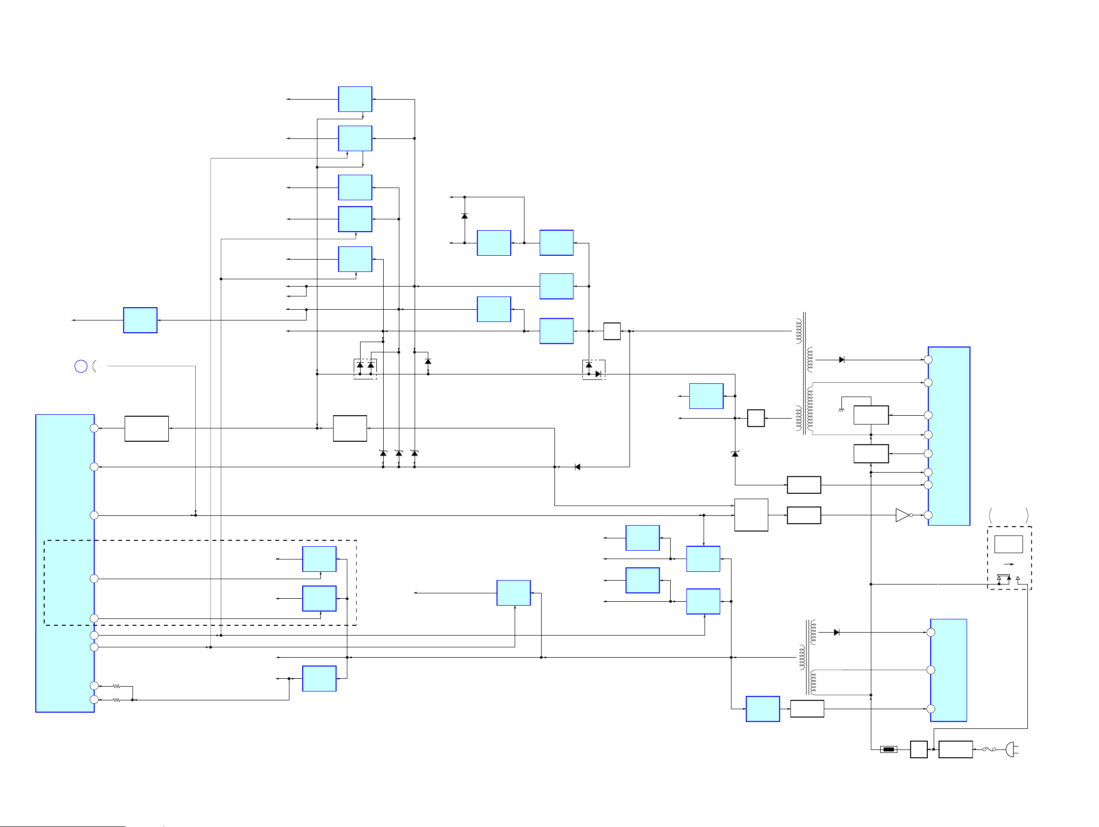
6,*1$/3$7+
&'3/$<
86%
5FKLVRPLWWHGGXHWRVDPHDV/FK
237,&$/3,&.83%/2&.
.+0&$$
92%%
92&&
92''
92((*
92$$
92)))
63
/,0,7
63
/'
3'
$8720$7,&
32:(5
&21752/
4
)2&8675$&.,1*&2,/'5,9(
6/('63,1'/(02725'5,9(
,&
&'9
&'03352&(6625
,&
922
92
,1
%,$6
6/
6/
92
92
,1
9
75.
75.
92
92
,1
)&6
)&6
9226
92
,1
24
087(
95 $
96 '
94 &
E
%
F
/'2
0',
952
'02
92
)02
752
9FOO
XO
;,
;
0+]
/,0,7
63,1'/(
6/('
24
&'/
5&+
%86
%86
&'%86
&'%86
95
%86
%86
&'%8694
&'%86
&'&/.
&'&&(
;567
&'B;567
&'B'5,9(5B087(
03B,5(4
6%6<
54 6%6<
$
&'0B/2$'B,1
59
&'0B/2$'B287
&/26(
23(1
&/26(6:
23(16:
&'0B23(1B6:
&'0B&/26(B6:
06%2$5'
6<67(0&21752//(5
,&
42%8&.
;&&(
5(4
4
92 '(&%866(/
'$7$6(/(&725
,&
6(/(&7
4
2
5
6
9
%86
6:,7&+
,&
%8))(5
,&
%8))(5
,&
%8))(5
,&
%86
6:,7&+
,&
65
66
49
/,0,7
00
00
/%
,2±,2'±'
65$0
,&
8%
OE
:(
&(6
'
'
86%2&
86%&21752//(5
,&
86%B7['B287
&1
2
'
'±
86%321
65$0&6
64
5'
6565:5
6665//%
65/8%
9%86
9%8632:(5
212))6:,7&+
,&
/2$',1*
02725'5,9(
,&
9%869
$,1
92 %&.
/5&.
94 *$7(
675(4
55 %868
56 %868
,86%6,
8;%B5['B,1
286%62
86%B576
2
,86%',
86%B&76
286%'2
86%B5(6(7
86%567
%868
%868
59 %8&.8
&&(8
96 5(48
±±
±±
±±
$±$$±$
±±
±±
±±
X2
;
;
0+]
'$7$
&/.
/287
5287
$,1
%&.,
/5&.,
*$7(
3,267B5(4
$287
%&.2
,1B6:
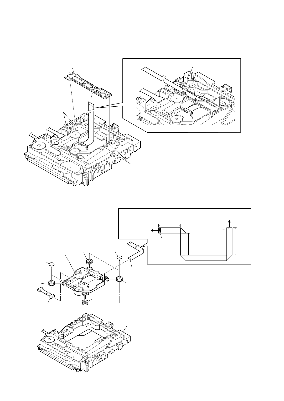
SECTION 5
DIAGRAMS
5-1. BLOCK DIAGRAM - CD, USB Section -
(Page 22)
Page 22
HCD-MX700Ni/MX750Ni
HCD-MX700Ni/MX750Ni
2222
R-CH
R-CH
CN01
AUDIO IN
J302
28
SDA27SCL
13
IN-L1
VOL L
1 IN-L2
IN-L3
VOL IIC_SDA/E2P-SDA
47
VOL IIC_CLK/E2P-CLK
48
AUDIO_LEVEL_INPUT
12
SEL L
25OUT L
24SB L
ELECTRICAL VOLUME,
INPUT SELECTOR
IC502
: TUNER
: CD PLAY
: iPod/iPhone
SIGNAL PATH
R-ch is omitted due to same as L-ch.
: AUDIO IN
A
B
CD-L
SP_L
7IN-L5
CN332
(iPod/iPhone Dock)
27
28
LINE AMP
IC503
BUFFER
IC515
R-CH
18
19
13
LINE-OUT-L
LINE-OUT-R
RXD
10
Acc ID
TXD
Acc PWR(3.3V)
30
DGND
iPod_RxD_IN
iPod_TxD_OUT
iPod_WAKE
3
75
iPod_DET
76
78 77
: DAB
DAB1
DAB TUNER
MODULE
S1_DIN
S1_DOUT
35 DAB TxD_OUT
36 DAB RxD_IN
AUDR
AUDL
LINE AMP
IC511
SYSTEM CONTROLLER
IC401 (2/4)
ANTENNA
DAB 75:
FM 75:
COAXIAL
ANTENNA
TU1
TUNER (FM)
L-OUT
DO/STEREO
CE
TUNED
DI
CLK
R-OUT R-CH
ST_CE
52
ST_CLK
54
ST_DI/STEREO
55
ST_DO
53
ST_TUNED
51
RDS DATA
RDS INT
RDS_DATA
56
RDS-INT
18
(AEP, UK)
(MX750Ni)
iPod POWER
DETECT
Q505
iPod +5V
20
Acc DET
iPod POWER
DETECT
Q506
iPod WAKE
UP DETECT
Q512
AUDIO INPUT
DETECT
Q504, 517
R-CH
32
IN-L45
66
+
Q510
SELECT SWITCH
IC512
1Y1
14
1Y012
1-COM
13
A
10
NET_L
E
SINGER_L
D
SINGER_ON
F
SINGER_ON
84
: LAN
5-2. BLOCK DIAGRAM - TUNER, iPod/iPhone, AUDIO IN Section -
(Page 21)
(Page 23)
(Page 23)
(Page 23)
(Page 23)
Page 23
HCD-MX700Ni/MX750Ni
HCD-MX700Ni/MX750Ni
2323
B
SP-L
SYSTEM CONTROLLER
IC401 (3/4)
: TUNER
SIGNAL PATH
R-ch is omitted due to same as L-ch.
C
SD
E
F
SPEAKERS
+
–
–
+
R
L
TB322
17
RESET_CD5SD
PWM_C
PWM_D
7
RESET_AB
S-MASTER_RESET
39
39
OUT_A
36
OUT_B
31
OUT_C
28
OUT_D
6 PWM_A
18
16
PWM_B
8
S-MASTER_DCP
OVER LOAD
DETECT
Q702, 703
PROTECT
DETECT
Q701
LED DRIVE
Q625
BYPASS
73
OVER LOAD
DETECT
Q752, 753
DIGITAL POWER AMP
IC707
11
OUTL1
9
OUTL2
6
OUTR1
4
OUTR2
STREAM PROCESSOR
IC705
A/D CONVERTER
IC711
34
TA_LINE_MUTE
MUTING
Q106
MUTING
CONTROL
SWITCH
Q507, 508
82
PROTECT
DETECT
Q516
X703
49.152MHz
S-MASTER_DATA
40
SCDT
21
S-MASTER_SHIFT
42
S-MASTER_LATCH
43
S-MASTER_PG_MUTE
37
S-MASTER_SOFT_MUTE
38
S-MASTER_NSP_MUTE
44
SCSHIFT22SCLATCH23PGMUTE20SOFTMUTE19NSPMUTE
18
S-MASTER_INIT
45
INIT
27
31 DATA2 AINL
1 AINRR-CH
R-CH
SCLK
12
SDTO
9
LRCK
10
MCLK
11
BCK
30
LRCK
29
XFSIIN
36
XFSOIN
48
CLOCK
BUFFER
IC709
CLOCK
SHIFT
IC703
LCD601
LIQUID
CRYSTAL
ELEMENT
1
FL/LCD DO2FL/LCD SCL3FL/LCD CS61FL/LCD RESET
SIRCS
REMOTE
CONTROL
RECEIVER
IC622
4
I_KEY WAKE UP_POWER & DISPLAY
74
VOLUME_JOG
72
BCo_POWER
21
KEY_1, KEY_2
X402
5MHz
Xout
Xin
13 15
X401
32.768kHz
Xcout
Xcin
11 10
S621 - 632
(PANEL KEYS)
70, 71
2
LED DRIVE
Q623
STBY_LED
46
STANDBY
VOLUME
KEY_1
D624
LED DRIVE
Q624
LCD_BACKLIGHT
41
(LCD BACK LIGHT)
EVER +3.3V
D625, 626
ROTARY
ENCODER
RV621
MOD1
WIRELESS LAN MODULE
AV2CTR (ADA_LRCK)
AV2CLK (ADA_BCK)
AV2DATA0
A23
SPI_OUT (DA810)
SPI_DIN (DA810)
SPI_CLK (DA810)
SPI_NCS0
A22 (DA810)
PDOUT0
PDOUT1 (DA810)
CN1006
NETWORK
TX+
TX-
RX+
RX-
1
2
3
6
ETH TX+
ETH TX-
ETH RX+
ETH RX-
D/A CONVERTER
IC1001
4 LRCKI
AV2CTR1 (ADA_MCK)
1MCLK
2 BICK
6SMUTE
AV2DATA2
9SDTO
3SDTI
R OUT
10
L OUT
11
NET_L
R-CH
6 BCo_SPI_DIN
5 BCo_SPI_DOUT
7 BCo_SPI_CLK
23 BCo_SPI_CS
68 BCo_SPI_READY
NRESET_MOD
BCo_RESET
67 BCo_SPI_REQ
MCLK
11
SCLK
12
A/D CONVERTER
IC1005
RESET
13
LRCK
10
AINR
1
AINL
2
R-CH
25
RSTN
2
24
iPod CP IIC SDA
SINGER_ON
D
SINGER_L
GR
22
iPod CP IIC SCL26iPod CP RESET
EEPROM
IC402
12
I2C_SCL
4
RESET
13
I2C_SDA
ANT1
: LAN
5-3. BLOCK DIAGRAM - NETWORK, OUTPUT, PANEL Section -
(Page 22)
(Page 24)
(Page 22)
(Page 22)
(Page 22)
Page 24
HCD-MX700Ni/MX750Ni
HCD-MX700Ni/MX750Ni
2424
20
12
POWER ON 63
D923
POWER CONTROL
IC11
D14
D603
EVER +4V
EVER +3.3V
(AC IN)
F1
LINE FILTER
T1
RECT
D1
TH1
D902
15 VS
18 VD
1 VSENSE
2 F/B
16 VG-H
12 VG-L
8VC1
POWER CONTROL
IC601
5 DRAIN
2FB
4VCC
ISOLATOR
PC11
ISOLATOR
PC602
ISOLATOR
PH601
T031
MAIN POWER
TRANSFORMER
T603
SUB POWER
TRANSFORMER
POWER
ON/OFF
CONTROL
Q901 - 903
SWITCHING
Q012
SWITCHING
Q011
SHUNT
REGULATOR
IC909
RECT
D904
+12V
REGULATOR
IC710
Q601
9OCP
D905
AMP +27V
AMP +12V
RESET
69
AC_DET
D927 D914
83
POWER_PROTECT
+3.3V
REGULATOR
IC405
AMP +3.3V
+3.3V
REGULATOR
IC704
VBUS +5V
+5V
REGULATOR
IC506
+3.3V
+3.3V
REGULATOR
IC1004
iPod +5V
LED +7V
AMP +1.8V
+1.8V
REGULATOR
IC712
CD D +3.3V
CD D +1.5V
+1.5V
REGULATOR
IC102
DAB +3.3V
+3.3V
REGULATOR
IC671
A +9V
M +7V
+9V
REGULATOR
IC905
A +5V
+5V
REGULATOR
IC908
+1.2V
REGULATOR
IC1003
+7V
REGULATOR
IC904
+3.3V
REGULATOR
IC1002
RECT
D903
D911
D922
D1002
AC-CUT
49
DAB-POWER_3.3
USB +3.3V
+3.3V
REGULATOR
IC509
85
BOLERO/iPod_ON
86
ZIPANG_ON
DAB +1.2V
+1.2V
REGULATOR
IC672
50
DAB-POWER_1.2
C
SD
PROTECT
DETECT
Q904
OVER CURRENT
PROTECT
Q509
SYSTEM CONTROLLER
IC401 (4/4)
D913
(MX750Ni)
+3.3V
REGULATOR
IC508
+5V
REGULATOR
IC510
CD A +3.3V
+3.3V
+1.2V
+3.3V
REGULATOR
IC505
CD +5V
+5V
REGULATOR
IC504
A/D +3.3V
+3.3V
REGULATOR
IC702
S001
220
l
240V
110
l
12V
VOLTAGE
SELECTER
Latin American,
Brazilian
5-4. BLOCK DIAGRAM - POWER SUPPLY Section -
(Page 23)
Page 25
HCD-MX700Ni/MX750Ni
HCD-MX700Ni/MX750Ni
2525
For Schematic Diagrams.
Note:
• All capacitors are in μF unless otherwise noted. (p: pF) 50
WV or less are not indicated except for electrolytics and
tantalums.
• All resistors are in Ω and 1/4 W or less unless otherwise
specifi ed.
• f : Internal component.
• 2 : Nonfl ammable resistor.
• C : Panel designation.
THIS NOTE IS COMMON FOR PRINTED WIRING BOARDS AND SCHEMATIC DIAGRAMS.
(In addition to this, the necessary note is printed in each block.)
• A : B+ Line.
• B : B– Line.
• Voltages and waveforms are dc with respect to ground
under no-signal (detuned) conditions.
– BD96/BD96U Board –
no mark : CD PLAY
– Other Boards –
no mark : TUNER FM
< > : TUNER DAB
* : Impossible to measure
• Voltages are taken with VOM (Input impedance 10 MΩ).
Voltage variations may be noted due to normal production
tolerances.
• Waveforms are taken with a oscilloscope.
Voltage variations may be noted due to normal production
tolerances.
• Circled numbers refer to waveforms.
• Signal path.
F : TUNER
J : CD PLAY
d : USB
i : iPod/iPhone
f : AUDIO IN
L : DAB
G : LAN
• Abbreviation
AUS : Australian model
BR : Brazilian model
CND : Canadian model
E2 : Latin American model
TW : Taiwan model
For Printed Wiring Boards.
Note:
• X : Parts extracted from the component side.
• Y : Parts extracted from the conductor side.
• f : Internal component.
• : Pattern from the side which enables seeing.
(The other layers’ patterns are not indicated.)
• Indication of transistor.
Caution:
Pattern face side:
(SIDE B)
Parts face side:
(SIDE A)
Parts on the pattern face side seen
from the pattern face are indicated.
Parts on the parts face side seen from
the parts face are indicated.
Caution:
Pattern face side:
(Conductor Side)
Parts face side:
(Component Side)
Parts on the pattern face side seen
from the pattern face are indicated.
Parts on the parts face side seen from
the parts face are indicated.
• Circuit Boards Location.
• Abbreviation
AUS : Australian model
BR : Brazilian model
CND : Canadian model
E2 : Latin American model
TW : Taiwan model
Note:
The components identifi ed by mark 0 or dotted
line with mark 0 are critical for safety.
Replace only with part
number specifi ed.
Note:
Les composants identifi és
par une marque 0 sont
critiques pour la sécurité.
Ne les remplacer que par
une pièce portant le numéro spécifi é.
C
Q
B
E
These are omitted.
LCD board
POWER board
IP board
MAIN board
JACK board
JUNCTION board
SP board
KEY board
USB board
DAB board (MX750Ni)
MODULE (DAB TUNER) (MX750Ni)
NET board
WIRELESS LAN MODULE
TUNER (FM)
BD96U board
MS-203 board
Page 26

HCD-MX700Ni/MX750Ni
HCD-MX700Ni/MX750Ni
2626
B
E
2
24
1
23
16
1
5
1
4
2
26
27
1
1
148
7
122
23 44
R401
R402
R403
R404
R210
R407
R408
R409
R215
R218
R219
R410
R411
CN201
R412
R415
R418
R419
CN401
CN402
R420
R422
R425
R430
R431
C202
R433
C203
C204
R435
R437
C207
C208
R439
C404
R440R441
C405
C213
C408
C214
R445
R446
C216
CL102
R447
CL103
R448
CL104
CL105
CL106
CL107
C410
CL108
C411
C414
C415
CL301
CL302
CL303
CL304
CL305
CL306
R457
CL113
R458
CL114
CL115
CL117
CL118
CL501
C422
CL502
CL503
C423
CL504
C424
CL505 CL506
R463
CL507
R464
CL508
CL509
R465
R466
CL122
R467
CL123
R468
CL124
R469
CL125
CL510
CL511
CL512
CL513
CL514
R470
CL515
C436
CL516
C437
CL518
CL519
R479
CL520
CL521
CL522
R480
D401
SL301
SL302
D403
SL303
SL304
IC201
IC402
IC403
IC406
R101
R302
R305
R308
R501
R503
R504
R505
R311
R506
R507
R508
R314
R509
R122
R125
R510
R511
CN301
R512
R513
R514
R516
R518
R130
R519
R131
CN501
R136
R520
R521
C101
C103
C104
C105
R143
R144
C108
R145
R146
R147
R149
C302
C303
C110
C305
R150
C309
C501
C119
C502
C503
C504
C505
C506
C507
C508
CL201
CL202
C123
CL203
C124
CL204
C125
CL205
C126
CL206
C127
CL207
C128
CL208
C129
CL209
C513
CL401
C515
CL402
CL403
C518
CL404
CL210
CL405
CL211
CL406
CL212
CL407
C133
CL213
CL408
C134
CL214
CL409
C135
CL215
CL216
C137
C521
C139
CL410
CL411
CL412
CL413
CL414
CL415
C141
CL416
CL417
C145
C536
C157
C158
C159
C160
Q201
SL201
ET501
ET504
R201
R202
R203
R204
R205
R206
R207
R208
R209
B
USB BOARD
CN315
C
MAIN BOARD
CN408
A
MAIN BOARD
CN413
7
1
8
14
1
34
5
1-882-088-
11
(11)
BD96U BOARD
(SIDE A)
(CHASSIS)
(CHASSIS)
OPTICAL
PICK-UP
BLOCK
(KHM-313CAA)
M
M
(SLED)
(LIMIT)
(SPINDLE)
16
A
B
C
D
E
1 2 3 4 5 6 7
5-5. PRINTED WIRING BOARD - BD96U Board (Side A) -
• : Uses unleaded solder.
• See page 25 for Circuit Boards Location.
(Page 33)
(Page 40)
(Page 33)
Page 27

HCD-MX700Ni/MX750Ni
HCD-MX700Ni/MX750Ni
2727
28
7
8
1
22
21
15
14
30
29
1
100
76
75
26
25
50
51
1
45
8
1
45
8
1
148
7
18
916
BE
1
100
76
75
26
25
50
51
R211
R212
R213
R214
R216
R217
R413
R414
R220
R221
R416
R222
R223
R224
R225
R226
R227
R228
R229
R421
R230
R231
R432
R434
R436
R438
C403
C210
C211
R442
C406
C212
C407
R443
R444
C409
R449
X401
C412
C413
R450
R451
R452
R453
R454
R455
R456
R459
C420
C421
C425
C426
C434
C435
R471
C438
R481
IC202
IC203
IC401
IC404
IC405
R102
R103
R104
R105
R106
R107
R108
R109
R112
R306
R113
R116
R502
R120
R121
R316
R124
R126
R127
R128
R515
R133
R134
R135
R137
R138
R139
R140
R141
R142
C106
C107
C109
C111
X101
C112
C113
C114
R151
C115
R152
C116
R154
C118
R155
R156
R157
R158
R159
C122
C514
C130
C131
C132
C136
C138
C142
C143
C148
C149
Q401
IC101
IC102
IC301
C512
1
342
1-882-088-
11
(11)
BD96U BOARD
(SIDE B)
A
B
C
D
1 2 3 4 5 6 7
5-6. PRINTED WIRING BOARD - BD96U Board (Side B) -
• : Uses unleaded solder.
• See page 25 for Circuit Boards Location.
Page 28

HCD-MX700Ni/MX750Ni
HCD-MX700Ni/MX750Ni
2828
1
2
BOARD
BD96U
(2/2)
11
IC B/D
IC B/D
BOARD
(2/2)
BD96U
12
BOARD
(2/2)
BD96U
13
003.3
0
3.3
00000
1.5
1.6
1.6
1.6
3.3
0
0
0
0
3.3
0
0
0
0
3.3
3.3
0
1.5
1.5
3.3
1.6
1.6
1.6
3.3
1.4
1.6
1
1.7
1.6
1.6
1.6
1.6
0
0
1.6
1.6
1.6
3.3
2.3
2.3
1.8
1.8
1.8
1.8
1.8
1.2
1.8
1.602.4
1.6
1.6
3.3
1.6
1.7
1.7
1.6
1.9
1.3
3.3
1.5
1.5
1.5
3.3
1.5 3.3
3.3
3.1
6.9
6.9
3.1
3.1
3.1
1.6
1.6
1.6
1.6
2.9
3.5
1.6
6.9
3.3
1.6
3.1
3.1
1.6
2.151.8
2.1 2.1
1.8
2.1
2.1
2.1
1.8
2.1
1.8
2.1
5
1.8
2.1
2.1
2.5
2.5
2.5 2.5
5
2.1
1.8
2.1
2.5
2.5
2.3
1.9
3
1 2 3 4 5 6 7 8 910111213141516171819202122232425
26
27
28
29
30
31
32
33
34
35
36
37
38
39
40
41
42
43
44
45
46
47
48
49
50
51525354555657585960616263646566676869707172737475
76
77
78
79
80
81
82
83
84
85
86
87
88
89
90
91
92
93
94
95
96
97
98
99
100
TC94A70FG-101
IC101
AVSS3
RFZI
RFRP
SBAD
FEO
TEO
TEZI
AVDD3
FOO
TRO
VREF
FMO
DMO
VSSP3
VCOI
VDDP3
VDD1
VSS1
FGIN
IN_SW
/DFCT
XVSS3XIXO
XVDD3
DVSS3
ROUT
DVDD3
DVR
LOUT
DVSS3
VDDT3
VSS1
VDD1
VDDM1
SRAMSTB
XRST
BUS0
BUS1
BUS2
BUS3
BUCK
XCCE
TEST
IRQ
ST_REQ/CKO
AOUT2
REQ
PIO1/ST_REQ
PIO2
GATE
VSS1
VDDT3
SBSY
FOK
IPF
/LOCK
ZDET
GPIN
MS
DOUT
AOUT1
BCKO
LRCKO
AIN
BCKI
LRCKI
VDD1
VSS1
AWRC
PVDD3
PDO
TMAXS
TMAX
LPFN
LPFO
PVREF
VCOF
PVSS3
SLCO
RFI
RFRPI
RFEQ0
VRO
RESIN
VMDIR
TESTR
AGCI
RFO
RVDD3
LDO
MDI
RVSS3
C
A
D
B
F
TNPC
E
CL106
CL107
CL108
CL118
CL117
CL115
CL114
CL113
CL102
CL103
CL104
0.033
C116
0.033
C122
1M
R134
10k
R131
16.934MHz
X101
28 27 26 25 24 23 22 21 20 19 18 17 16 15
141312111098765432129
30
BA5826HFP-E2
IC301
VO1-
VO1+
IN1
RESET
REGB
REGOUT
MUTE
GND
IN2’
IN2
VO2+
VO2-
GND
OPOUT OPIN
RESETt
VO3-
VO3+
IN3
IN3’
VCC
VCC
BIAS
IN4’
IN4
VO4+
VO4-
GND
GND GND
SL301
SL302
SL304SL303
CL105
CL122
CL123
CL124
CL211
CL212
CL213
CL214
CL209
CL210
CL206
CL205
CL208
CL207
CL204
CL203
2SA2119K
Q201
CL201
CL202
SL201
43
12
MM3404A15URE
IC102
CE
VSS Vout
VDD
NJM13403V(TE2)
IC201
12
3
4
V+
56
7
89
10
11
GND
121314
NJM2740V
IC203
1234
V-
5
6
78
V+
NJM2740V
IC202
1234
V-
5
6
78
V+
1
2
3
4
5
6
7
8
9
10
11
12
13
14
15
16
17
18
19
20
21
22
23
24
24P
CN201
GND (LD)
LD (650)
NC
NC
PD
LD (780)
VR (650)
VR (780)
NC
VOE/E+G
VCC
VC
GND (PDIC)
VOF/F+H
VOB/B
VOA/A
RF
(LO:DVD.HI:CD)MSW
VOD/D
VOC/C
TRKTRK+
FCS+
FCS-
1
2
3
4
5
6
6P
CN301
SP-
SP+
LIMIT
LIMIT
SL-
SL+
0
R127
0
R136
L-OUT
R-OUT
AVDD3.3V
AGND
DACGND
AVDD5V
VM
MGND
DVDD-Z
DGND
CL215
CL125
CL216
CL301
CL302
CL303
CL304
CL305
CL306
0.01C114
0.015
C115
15k
R108
0
R109
100
R125
100k
R130
0
R152
0.1
C134
0.1
C135
0.1C123
100
R126
47k
R113
47p
C118
0
R121
0
R124
0
R120
0
R107
0
R104
0
R106
0
R102
0
R105
0
R103
0.01C106
0.1C112
2200pC111
0.015C109
0.1C113
0.01
C110
68p
C107
1000pC108
0.1
C104
0.1
C103
1
C101
10V
100
C105
22k
R101
C119
0.1
C160
1000p
10
C214
10
C216
100
R140
100
R141
100k
R144
100k
R145
100k
R143
100k
R146
100k
R149
100k
R150
10kR147
100R139
0.1
C143
100R151
100
R156
100
R157
100
R154
100
R155
100
R159
100
R158
0
R122
1k
R135
5p
C1365pC138
0.1
C137
C157
1000p
C158
1000p
10k
R133
0.1C133
0.1
C142
1
C148
1M
R137
47
R142
6.3V
22
C141
0.1
C145
1
C149
0.1
C139
C159
1000p
1M
R138
470p
C126
470p
C125
0.1
C131
0.1
C127
0.1
C124
0.047
C128
0.047
C129
0.1C130
2200p
C132
220R128
0.1
C213
0.1
C211
0.1
C212
R314
0
10k
R311
0
R306
15k
R305
47k
R316
10V
220
C309
0.1
C305
0.1
C303
0.1
C302
39k
R308
10k
R302
10kR229
10k
R231
10k
R227
10k
R230
10k
R228
10k
R221
100
R205
10
C208
1
C204
10V
100
C203
100k
R204
10k
R224
10k
R226
10k
R222
10k
R223
10k
R225
10k
R220
10k
R213
10k
R214
10k
R217
10k
R216
1
C207
1
C210
1k
R212
10k
R218
10k
R219
10k
R210
1k
R211
10k
R215
10k
R208
10kR209
10k
R206
10k
R207
0
R203
1
R201
1000p
C202
3.3
R202
DATA
ST_REQ
SBSY
REQ-Z
RST-Z
BUS0-Z
BUS1-Z
BUS2-Z
BUS3-Z
BUCK-Z
CCE-Z
CLK
LRCK
GATE
M-MUTE
AIN
BCK
CD-MP3 PROCESSOR
IC101
IC102
+1.5V REGULATOR
IC301
FOCUS/TRACKING COIL DRIVE,
IC201
BUFFER
IC202
IC203
BD96U BOARD (1/2)
1
2
AUTOMATIC
POWER CONTROL
BUFFER
BUFFER
SLED/SPINDLE MORTOR DRIVE
(SPINDLE)
M
M
(SLED)
(LIMIT)
OPTICAL
PICK-UP BLOCK
(KHM-313CAA)
E
11
J
3
K
D
F
14 15
M
L
8
G
7 18
I
13
A
109
C
194
H
16 1726
B
51 12
330k
R112
5.6k
R116
1
6
5-7. SCHEMATIC DIAGRAM - BD96U Board (1/2) -
• See page 30 for Waveforms. • See page 46 for IC Block Diagrams. • See page 51 for IC Pin Function Description.
(Page 29)
(Page 29)
(Page 29)
Page 29

HCD-MX700Ni/MX750Ni
HCD-MX700Ni/MX750Ni
2929
C
MAIN
(2/4)
BOARD
CN408
A
MAIN
(2/4)
BOARD
CN413
B
USB
CN315
BOARD
3
BOARD
12
BD96U
(1/2)
IC B/D
BOARD
(1/2)
BD96U
13
IC B/D
IC B/D
IC B/D
11
BOARD
BD96U
(1/2)
0
3.3
0
0
3.3
3.3
3.3
0
0
0
0
3.3
0
0
0
3.3
000
0
0
0
0
0
0
0
3.3
3.303.3
0
0
0
0
3.3
0
0
3.3
0
3.3
00
00
00
0 3.3
0 3.3
3.3 3.3
0.2 0.2
0.20.2
0.20.2
0.20.2
3.3
0.10.3
3.3
0.3 0.1
0.3 0.1
0.3 0.1
3.3
00
00
00
00
0.3
0.2
0.2
0.2
0.2
0.3
0.3
0.3
0
0
0
0
3.3
3.3
3.3
3.3
3.3
3.3
3.1
0
0
3.1
3.3
0
0
0
0
0
3.3
3.3
3.3
0
0
0
0
3.3
3.3
3.3
3.3
0
0
0
0
0
3.3
0
0
0
0
0
0
0
0.2
0.2
0.2
0.2
0.1
0.1
0.1
3.3
0.1
1.4
1.6
3.300
3.3
3.3
3.3
3.3
3.3
3.3
000000000
0
5.1
3.3
5.1
3.3
92CD28AFG-7FU8 (M
IC401
1
USB-RST2I-USB-DI3INT14INT25INT36DVCC3B7XT18XT29PWE10DVSS1B11DVCC1B12RVOUT113RVIN14RVIN15RVOUT216DVCC1A17DVSS1A18D019D120D221D322D423D524D625D7
26
DVSS
27
DVCC3A
28
D8
29
D9
30
D10
31
D11
32
D12
33
D13
34
D14
35
D15
36
A0
37
A1
38
A2
39
A3
40
A4
41
A5
42
A6
43
A7
44
DVSS
45
DVCC3A
46
A8
47
A9
48
A10
49
A11
50A12
51
A1352A1453A1554A16
55
BUS0-U56BUS1-U57BUS2-U58BUS3-U
59
BUCK-U
60
CCE-U
61
A23
62
DVSS
63
DVCC3A
64RD65
SRWR
66
SRLLB
67
SRLUB
68
TA0IN
69
BOOT
70
SRAM-CS
71
LRCK
72
AM1
73X274
DVSS
75
X1
76 DVCC3A
77 USBOC
78 USBPON
79 D+
80 D81 AM0
82 X1USB
83 DVSS
84 O-USB-D0
85 DATA
86 CLK
87 O-USB-SO
88 I-USB-SI
89 SPCLK
90 SO0
91 SI0
92 BCK
93 A-IN
94 GATE
95 DVCC3A
96 REQ-U
97 ST-REQ
98 PG1
99 PG0
100 DVSS
44
38
39
40
41
42
43
7
6
5
4
3
2
1
37
36
35
34
33
32
8
9
10
11
28
29
30
31
17
16
15
14
13
12
27
26
25
24
2322
21
20
19
18
CY7C1021CV33-10ZXIT
IC402
A15
A14
A13
A12
A11
CE
I/O0
I/O1
I/O2
I/O3
VCC
GND
I/O4
I/O5
I/O6
I/O7
WE
A10
A9
A8
A7
NC
NC
A6
A5
A4
A3
NC
I/O8
I/O9
I/O10
I/O11
VCC
GND
I/O12
I/O13
I/O14
I/O15
LB
UB
OE
A2
A1
A0
9MHz
X401
TC74VHC157FT(EKJ)
IC405
1
SELECT
21A31B41Y52A62B72Y8
GND
9
3Y103B113A124Y134B144A15ST16VCC
TC74HC4066AFT(EL)
IC403
1
1I/O21O/I32O/I42I/O52C63C7GND
8
3I/O93O/I104O/I114I/O
12
4C131C
14
VCC
TC74HC4066AFT(EL)
IC404
1
1I/O21O/I32O/I42I/O52C63C7GND
8
3I/O93O/I104O/I114I/O
12
4C131C
14
VCC
RT1N141C-TP-1
Q401
0.1
C422
0.1
C423
DZ2J036M0L
D401
DZ2J036M0L
D403
1
2
3
4
4P
CN402
VBUS_GND
D+
D-
VBUS_VCC
5P
CN401
1VM7V
2MGND
3USB5V
4DGND
5DGND
E
ET501
E
ET504
1
2
3
4
5
6
7
8
9
10
11
12
13
14
15
16
17
18
19
20
21
22
23
24
25
26
27
27P
CN501
AVDD5V
AVDD3.3V
R-ch
DACGND
L-ch
AGND
RST-Z
BUS0
BUS1
BUS2
BUS3
BUSCK
CCE
REQ
SBSY
M-MUTE
DVDD-Z
DGND
DVDD-EVER3.3V
DVDD-B
BUS_SEL
DGND
DO
DI
USB-SO
USB-SI
USB-RST
VM
MGND
DGND
DVDD-Z
AVDD5V
AVDD3.3V
DACGND
AGND
L-OUT
R-OUT
CL522
CL521
CL520
CL519
CL518
CL516
CL514
CL513
CL512
CL511
CL510
CL509
CL508
CL507
CL506
CL505
CL503
CL501
CL502
CL504
CL515
CL406
CL407
CL408
CL409
CL401
CL402
CL403
CL404
CL405
0
R503
0
R502
0
R501
0
R515
CL410
CL411
CL412
CL413
CL414
CL415
CL416
0
R459
BD2220G-TR
IC406
1
VIN
2
GND
3
EN
4OC5
VOUT
CL417
27R414
100
R442
27R413
10k
R440
10k
R441
0
R410
10k
R409
100
R444
10k
R407
100
R443
4.7k
R411
4.7k
R412
15k
R404
15k
R403
100k
R481
0.1
C438
C434
1000p
0.1
C404
0.1
C405
10k
R480
0.1
C403
100
R458
100R457
100R447
100R446
100R448
100
R445
100k
R436
100k
R434
100k
R438
100k
R432
0.1
C412
C435
1000p
0R419
4.7k
R431
4.7k
R430
4.7k
R437
100
R420
10k
R422
4.7k
R439
100k
R425
4.7k
R435
4.7k
R433
0.1
C421
0.1
C420
47
R449
47
R456
47
R455
47
R451
47
R454
47
R453
47
R452
47
R450
47
R464
47
R465
47
R466
47
R463
R467
47
R468
47
47
R469
47
R470
10V
100
C513
0.1
C514
100
R416
22p
C406
33p
C407
0.1
C426
0.1
C424
0.1
C425
10k
R471
100
R520
100
R506
100R512
100
R519
100R509
100
R507
100R511
100
R508
100
R518
100
R521
100
R516
100R510
C521
0.1
0.1
C504
10V
100
C501
0.1
C506
0.1
C505
10V
100
C502
10V
100
C503
0.1
C413
0.1
C409
100R513
100R514
0.1
C411
0.1
C414
16V
10
C415
16V
10
C410
0.1
C408
4.7k
R421
10k
R415
100
R418
C515
0.1
100k
R408
1
C437
1k
R479
1
C436
C536
1
2200p
C507
2200p
C508
100
R504
100
R505
C518
0.1
0
R401
0
R402
D0D1D2D3D4D5D6
D7
D8
D9
D10
D11
D12
D13
D14
D15
A0
A1
A2
A3
A4
A5
A6
A7
A8
A9
A10
A11
A15
A14
A13
A12
A11
SRAM-CS
WR
A10
A9
A8
A7 A6
A5
A4
A3
LB
UB
RD
A2
A1
A0
D7
D3
D2
D1
D0
D4
D5
D6
D8
D9
D10
D11
D12
D13
D14
D15
A12
A13
A14
A15
DATA
CLK
ST_REQ
DO-B
DI-B
REQ-B
BUS0-B
BUS1-B
BUS3-B
BUS2-B
BUS2-Z
BUS2-Z
BUS3-Z
BUS3-Z
BUS1-Z
BUS1-Z
BUS0-Z
BUS2
BUS0
BUS0-Z
CCE
CCE-Z
BUCK
BUCK-Z
REQ
BUS1
RST-B
SRAM-CS
RXD-B
TXD-B
REQ-B
BOOT
AM0
TXD-B
RXD-B
RST-B
RXD-B
TXD-B
DI-B
DO-B
BUS_SEL
M-MUTE
SBSY
REQ
CCE
BUCK
BUS3
BUS2
BUS1
BUS0
BOOT
AIN
GATE
BUS0-B
BUS1-B
BUS2-B
BUS3-B
BUCK-B
CCE-B
BCK
AM0
LRCK
CCE-B
BUCK-B
REQ-Z
BUS3
BUS_SEL
RST-B
UB
WR
LB
RD
RST-Z
C512
0.1
USB CONTROLLER
IC401
S-RAM
IC402
DATA SELECTOR
IC405
BUS SWITCH
IC404
IC406
VBUS POWER
(CHASSIS)
(CHASSIS)
BD96U BOARD (2/2)
ON/OFF SWITCH
INVERTER
IC403
BUS SWITCH
1
2
E
11
J
3
K
D
F
14 15 21
M
L
8
G
7 18
N
I
13
A
109
C
194
H
16 1726
B
51 12 20
5-8. SCHEMATIC DIAGRAM - BD96U Board (2/2) -
(Page 28)
(Page 35)
(Page 41)
(Page 28)
(Page 28)
(Page
35)
• See page 30 for Waveforms. • See page 46 for IC Block Diagrams. • See page 51 for IC Pin Function Description.
Ver. 1.1
Page 30

HCD-MX700Ni/MX750Ni
HCD-MX700Ni/MX750Ni
3030
• Waveforms
– BD96U Board – – MAIN Board –
5-9. PRINTED WIRING BOARD - DAB Board (MX750Ni) -
(Page 33)
– NET Board –
•
: Uses unleaded solder.
• See page 25 for Circuit Boards Location.
IC101 wf (XO)
1
(CD play mode)
59.1 ns
2 V/DIV, 50 ns/DIV
2 IC101 il (RFO)
4.6 Vp-p
IC401 qa (Xcout)
qa
IC401 qd (Xout)
qs
1 V/DIV, 20 Ps/DIV
(CD play mode)
500 mV/DIV, 1 Ps/DIV
IC401 ud (X2)
3
(CD play mode)
0.9 Vp-p
qd
3.6 Vp-p
111 ns
1 V/DIV, 50 ns/DIV
qf
200 ns
1 V/DIV, 100 ns/DIV
IC705 rk (XFSOIN)
20.6 ns
1 V/DIV, 10 ns/DIV
IC711 0 (LRCK)
30.8 Ps
1.9 Vp-p
3.2 Vp-p
3.1 Vp-p
IC1001 1 (MCLK)
wa
1 V/DIV, 20 ns/DIV
IC1001 2 (BICK)
ws
356 ns
1 V/DIV, 200 ns/DIV
IC1001 4 (LRCK)
wd
22.6 Ps
1 V/DIV, 10 Ps/DIV
44.2 ns
2.6 Vp-p
3.3 Vp-p
3.4 Vp-p
1 2 3 4
DAB1
DAB TUNER
MODULE
A
B
JW655
DAB BOARD
C675
1
2
C681
JW654
C690
R678
C673
13
45
C672
R676
C691
C674
R681
R672
C688
R679
C682
C689
R677
CN672
C679
IC672
R673
C678
C677
15
IC671
C
CN01
R680
R675
ANTENNA
DAB 75:
JL672
29
30
C683
JW656
C684C685
C686
JL673
JL671
JL679
JL678
JL674
FB671
2
1
JL675
H
CN671
JL677
JW653
MAIN BOARD
CN407
8
9
JL676
JW652
JW651
1-882-210-
11
(11)
IC711 qa (MCLK)
qg
IC711 qs (SCLK)
qh
4.7 Vp-p
20.8 Ps
1 V/DIV, 10 Ps/DIV
4.7 Vp-p
81 ns
1 V/DIV, 50 ns/DIV
4.9 Vp-p
324 ns
1 V/DIV, 200 ns/DIV
Page 31

HCD-MX700Ni/MX750Ni
HCD-MX700Ni/MX750Ni
3131
(2/4)
CN407
H
BOARD
MAIN
IC B/D
IC B/D
<2.8>
<3.9>
<1.2>
<1>
<3.2>
<1.3>
<3.9>
<3.3>
1
C674
1
C679
0.01
C673
100
R680
1
C678
54
321
TK11133CSCL-G
IC671
CONT
GND
NOISE VO
VI
100
R673
10k
R672
0.22
C672
JL678
JL679
JL677
JL676
30
28
26
24
22
20
18
16
14
12
10
8
6
4
2
29
27
25
23
21
19
17
15
13
11
9
7
5
3
1
30P
CN672
AUDL
AUD_SDOUTO
AUD_SFR
AUD_SFR
SPI_MOSO
SYS_RESET
SPICS2
S1_DIN
SCP2DATA
GPIOB4
GPIOB1
GPIOA5
GPIOC14
GND
1.2V
GPIOA14
S1_DOUT
SCP2CLK
GPIOB10
GPIOA12
GPIOC15
GPIOB11
GND
3.3V
AUDR
A_GND
AUD_SCLK
AUD_MCLK
SPI_MOSI
SP/PDIFOUT
1
C677
47k
R675
12345
SI-3010KM-TLS
IC672
CONTVIGNDVOF.B.
10k
R677
1k
R676
1k
R678
10k
R679
JL675
JL674
JL673
JL672
JL671
0
R681
C690
10p
C683
10p
C688
10p
C685
10p
C691
47p
C684
47p
C689
47p
C686
47p
0.1
C681
0.1
C675
0
FB671
6.3V
100
C682
1
2
3
4
5
6
7
8
9
9P
CN671
DAB_R
AGND
DAB_L
DAB_1.2V_ON
DAB_3.3V_ON
DGND
EVER4.0V
SIDO
SIDI
IC671
+3.3V REGULATOR
+1.2V REGULATOR
IC672
DAB BOARD
DAB1
DAB TUNER
MODULE
CN01
DAB 75:
ANTENNA
E
3
D
F
87
A
9
C
426
B
51
G
(Page 35)
5-10. SCHEMATIC DIAGRAM - DAB Board (MX750Ni) -
• See page 46 for IC Block Diagrams.
Page 32

HCD-MX700Ni/MX750Ni
HCD-MX700Ni/MX750Ni
3232
130
51 80
81
31
50
100
C1
B2
E2
C2
B1
E1
BE
BEBE
BE
BE
BE
BE
BEBE
BE
BE
BE
1
5
10
1620
6
11
15
BEBE
1
1617
32
1
45
8
1
5
51
51
14
58
1
24
25
36
3748
12
13
1
44
22
23
1
45
8
1
8
9
16
R400
R211
R213
R408
R215
R600
R601
R410
R411
R414
R221
R424
R426
R431
C201
R432
R433
R434
C204
C205
C206
R437
C207
R243
R438
C208
R439
C209
R248
C401
C402
C403
R440
R442
C406
R443
R444
R250
R251
R445
C217
R449 R450
R451
C416
R452
R453
C224
R454
R455
C419
R456
C226
R262
R457 R458
C229
R459
C806C807
C420
C421
R460
C230
CL505
C425
R462
CL506
CL507
R464
R466
CL700
CL701
R469
CL702
CL704
CL705
CL706
CL707
CL708
C240
CL709
C241
R472
C242
R473
R476
C246
C247
R478
CL710
CL711
CL713
CL717
R480
C252
R483
R484
R486
R487
TP723
CL720
R489
CL721
CL722
CL723
CL724
Q106
C261
C262
C263
C264
C265
R496
C266
R497
C267
C268
C269
C270
C271
C272
C273
Q504
C274
Q505Q506
Q507
Q508
Q509
C470
Q701
Q702
C473
Q703
C474
C475
C281
C476
Q512
C282
C283
C477
C284
C285
C479
C286
Q516
C863
C287
Q517
C288
C289
C480
IC401
C481
IC402
C482
C483
C484
C290
IC405
L701
C485
C291
C486
C292
C487
C293
C488
C294
C489
C490
C491
C492
C493
C494
C495
FB101
R101
R103
FB502
FB508
R111
FB509
R113
FB701
R115
Q752
Q753
FB704
FB512
FB513
R505
R506
FB519
R121
R125
R127
FB521
R706
R515
R516
R517
R519
R713
R137
R714
R520
R522
FB534
R524
C101
FB535
C104
C105
C106
C107
C108
R144
C109
R145
R532
R726
R727
R728
R537
R538
R539
C117
C500
C501
R731
C502
C503
R733
C504
C505
C506
R542
R736
R350
R352
R353
C124
R354
C701
R355
C126
R356
C703
R357
R163
C510
R358
C511
C129
CL400
C515
R745
C516
R746
C517
R747
R553
C518
C130
CL405
C519
R555
R556
CL406
R362
CL407
R364
X703
C520
C521
C522
R752
C524
R754
R561
C525
CL412
R756
C140
C529
C141
R371
C143
R374
C144
C721
C146
C530
C726
C727
CL420
CL421
R765
R572
CL423
R574
CL425
CL429
C731
R579
C733
C734
C736
C737
C543
CL430
C738
C544
C739
C545
R581
C546
R776
R582
R777
C547
CL434
R778
R585
C161
R391
R586
C162
R587
C163
R588
C164
CL439
R589
C165
C166
C167
C744
R780
C168
C745
C551
R781
C169
C746
R782
R783
R590
R591
CL441
C170
R594
C171
CL446
C172
C173
R597
C174
C751
R792
C563
R793
C759
C565
C566
C569
C181
C182
C183
C184
C185
C186
C187
C764
C570
C188
C765
C189
C571
C766
C572
C767
C574
C575
C577
C190
C191
C579
C192
CL467
C193
CL468
C194
CL469
C771
ET701
IC502
ET702
IC503
C778
C584
IC504
IC505
C585
C586
IC506
CL473
C587
IC508
IC509
C780
CL479
IC702
IC703
IC704
C784
C590
IC510
IC705
IC511
C785
C591
C592
IC707
C787
C593
C594
CL481
IC709
C595
IC515
CL482
C596
CL483
C597
CL484
C598
C599
IC711
C794
R201
R203
C808C809
R405
R407
R467
R468
R566
R567
R568
R573
R578
BE
C202
C245
C248
C249
C250
C257
C258
Q510
FB527
FB528
FB530
FB531
C102
R158
C512
C145
C148
C149
C150
C157
C158
C557
C558
C562
1
8
9
16
R564
1-882-114-
12
(12)
MAIN BOARD (COMPONENT SIDE)
13
45
1
3
4
5
13
4
5
1
3
4
5
1
3
4
2
1
8
14
7
1
3
4
5
13
4
5
(CHASSIS)(CHASSIS)
(US, CND, E2, BR, TW, AUS)
(MX750Ni)
(MX700Ni: AEP/MX750Ni: AEP, UK)
(AEP, UK)
(MX750Ni)
A
B
C
D
E
F
G
1 2 3 4 5 6 7 8 9 10 11
IC512
(EXCEPT US, CND, TW)
5-11. PRINTED WIRING BOARD - MAIN Section (1/2) -
• : Uses unleaded solder.
• See page 25 for Circuit Boards Location.
Page 33

HCD-MX700Ni/MX750Ni
HCD-MX700Ni/MX750Ni
3333
1
3
1
2
1
4
1
2
3
EP702
C820
CL714
L712
L762
CN702
CN703
C707
C708
C709
C710
C719
C720
C728
C729
C769
C770
C777
IC710
2
1
8
9
15
142
1
13
12
1
2
214
5
1
9
91
CN401
CN404
CN409
CN410
CN412
EP701
X402
W501
C527
C578
C580
IC507
14
51
13
CN402
CN413
CN417
C740
C747
C753
C798
8
9
1
2
10
11
2
1
8
9
1
9
CN405
CN406
CN407
CN414
EP501
C225
C125
C534
C567
C568
26
27
1
2
CN408
C220C221 C120C121
C735
C757
C781
X401
CN704
R401
R402
R403
R404
R212
R214
R409
D755
R412
R413
R416
R417
R418
R419
D765
R420
R422
R232
R427
R233
R428
R234
R429
R237
R430
R241
R435
R242
R436
R245
R246
R247
R249
R441
C408
C409
R446
R252
R447
R253
R448
C218
R254
R255
R257
R258
R259
C412
C418
C801
C804
JL401
JL402
JL403
JL404
JL405
JL406
C422
JL407
C423
JL408
C424
R461
JL409
R463
R465
JL410
JL411
JL412
JL413
JL414
JL415
JL416
JL417
R470
JL418
R471
JL419
R474
R475
C821
C822
R477
C823
JL420
C824
JL421
C825
JL422
C826
JL423
C827
JL424
C828
CL715
JL425
C829
CL716
JL426
JL427
CL718
JL428
CL719
JL429
R482
C254
R485
R488
JL430
JL431
JL432
JL433
JL434
R490
R491
R492
R493
R494
R495
C844
R498
C845
R499
C846
C847
TP739
C466
C469
TP741
TP743
TP745
C856
C857
C471
C472
C478
L702
L703
L704
C498
C499
L721
R102
R104
R108
FB504
FB505
FB506
FB507
R112
R114
FB702
FB703
FB510
R501
FB511
FB705
R502
FB706
R503
FB514
FB515
FB516
FB517
FB518
R120
R701
FB520
FB522
R513
FB523
R514
FB524
R518
R134
R711
R521
R523
R718
R529
R142
R143
R147
R724
R530
R725
R531
R533
R534
R535
R536
C118
R349
R157
R541
C509
R351
R546
R547
R548
C704
R359
C706
R743
R360
R557
R363
R558
R365
JL501
R559
C712
R366
JL502
C713
R367
JL503
JL504
R751
JL505
JL506
R753
JL507
C523
JL508
C718
R560
JL509
R562
C526
C528
R758
R565
R372
R373
JL510
JL511
C722
JL512
JL513
C723
JL514
C724
JL515
C725
C532
JL516
JL517
C533
R570
JL518
R571
JL519
C535
C536
R766 R767 R768
R769
R576
R577
JL520
JL521
JL522
JL523
R388
C540
JL524
R389
JL525
JL526
JL527
JL528
R774
JL529
R775
R583
R584
JL530
JL531
JL725
C741
JL726
JL532
JL727
JL533
JL728
JL534
R398
JL729
JL535
R399
JL536
JL537
JL538
R784
JL539
R785
R786
R592
R787
R593
JL730
R788
R789
R595
R596
JL540
R598
JL541
R599
JL542
C752
JL543
JL544
C754
JL545
D501
D502
JL546
C756
JL547
D503
C564
JL548
C758
JL550
C761
C762
C763
JL553
JL554
D705
JL555
D706
JL556
JL557
C768
JL558
JL559
JL561
C772
JL562
C773
JL563
C774
JL564
C581
C775
C582
C776
JL569
C779
JL570
JL571
JL572
JL573
JL574
JL575
C786
JL577
JL578
C788
JL579
C789
JL580
FB201
JL581
C792
JL582
IC712
C793
JL583JL584
C795
JL585
C796
JL586
C797
JL587
JL588
JL589
C799
R202
R204
R209
FB532
FB533
FB525
FB526
FB529
R406
R421
R423
R425
FB501
FB503
R569
R575
R397
11
10
1
2
CN411
R159
M
POWER
BOARD
CN904
L
SP BOARD
CN321
K
SP BOARD
CN321
I
POWER
BOARD
CN902
E
IP BOARD
CN331
G
LCD BOARD
CN651
O
NET BOARD
CN1005
F
JACK
BOARD
CN301
A
BD96U
BOARD
CN401
J
POWER
BOARD
CN905
C
BD96U BOARD
CN501
H
DAB BOARD
CN671
(CHASSIS)
(CHASSIS)
(CHASSIS)
1
34
2
1-882-114-
12
(12)
MAIN BOARD (CONDUCTOR SIDE)
TU1
TUNER
(FM)
SUPPLIED
WITH THE
ASSEMBLED
BLOCK
ANTENNA
FM 75:
COAXIAL
MS-203
BOARD
(NC)
(MX700Ni: AEP/MX750Ni: AEP, UK)
(US, CND, E2, BR, TW, AUS)
(EXCEPT AEP, UK)
(EXCEPT E2, TW, AUS)
(MX750Ni)
(US, CND, E2, BR, TW, AUS)
(MX700Ni: AEP/MX750Ni: AEP, UK)
A
B
C
D
E
F
G
1 2 3 4 5 6 7 8 9 10 11 12
N
NET BOARD
CN1004
(US, CND, TW)
5-12. PRINTED WIRING BOARDS - MAIN Section (2/2) -
Note: When the MS-203 board is damaged, exchange
the entire CDM85 (CD) ASSY.
(Page 30)
(Page 26)
(Page 26) (Page 44) (Page 40)
(Page 40)
(Page 44)
(Page 40)
(Page 44)
(Page 40)
(Page 42)
• : Uses unleaded solder.
• See page 25 for Circuit Boards Location.
(Page 38)
(Page 38)
Page 34

HCD-MX700Ni/MX750Ni
HCD-MX700Ni/MX750Ni
3434
12 11
BOARD
2
MAIN
(3/4)
BOARD
3
MAIN
(3/4)
BOARD
MAIN
1
(2/4)
IC B/D
IC B/D
G
BOARD
CN651
LCD
0
3.3
003.3
0
000000000
3.3
3.3
3.3
3.3
3.3
3.333.3
2.2
3.3
3.302.500
0
0
0
0
0
0
0
0
0
0
3.3
3.3
3.3
3.3
3.3
3.3
3.3
3.3
<3.3>
3.3
3.3
<3.3>
3.3
3.3
3.3
3.3
3.3
0
3.3
3.3
3.3
3.3
3.3
3.3
3.3
3.3
<3.3>
<0>
0
3.2
3.1
3.3
3.3
3.3
3.300.813.3
1.7
0.4
0
0
1.5
3.3
3.3
3.3
3.3
3.3
3.3
3.3
3.3
3.3
3.3
3.3
3.3
3.3
3.3
3.3
3.3
3.3
3.9
1.3
3.9
3.3
3.2
3.2
3.3
3.5
0
0
6.9
6.9
0
0
0
3.3
03.3
C535
0.1
1k
R463
ISA1235AC1-T112-1EF
Q509
1k
R520
10k
R519
10k
R583
R565
0.1
C530
R478
100
R477 100
1M
R474
100R404
32.768kHz
X401
10k
R409
10kR417
0.1
C416
R418
100
47kR420
100R421
100R423
100R425
10k
R412
C412
0.1
R529
10k
C540
0.1
100
R427
100
R428
CL400
CL429
CL430
10kR546
100
R444
100
R443
100
R442
100R441
100
R438
100R436
100R435
100
R431
100R432
4.7k
R429
4.7k
R430
100
R451
100
R452
100
R456
100R460
100R433
100R489
100R490
100R491
100
R492
220kR411
R465
10k
R577
100R493
100R494
100R495
100
R482
4.7k
R548
4.7k
R547
R475 10k
0
R413
CL441
CL446
R410 10M
18p
C511
1k
R483
47k
R536
1
2
3
4
5
6789
10
11
12
13
14
15
16
17181920
MFI341S2164
IC402
NC
MODE1
NC
RESET
VCC
NCNCNCNCNC
VSS
I2C_SCL
I2C_SDA
MODE0
NC
NCNCNCNCNC
C502
10p
1
C518
0.01
C563
100
R448
100R447
R450
100
100
R449
R461 100
R466 100
100
R401
100
R402
100
R403
100
R497
100R419
4.7k
R522
4.7k
R524
100
R453
100
R454
100R455
1kR457
1kR458
10kR557
10kR558
100R459
100R434
100R437
100R439
100R440
100R446
100R487
100R488
0.1
C529
R470 100
R471 100
10kR571
10k
R570
1k
R472
0.01
C472
10kR576
100R476
CL473
RT1N141C-TP-1
Q512
100R484
R480
1k
R556
47k
CL439
1k
R532
12 9876543
BA6956AN
IC507
VREF
OUT2
RNF
OUT1VMVCC
FIN
GND
RIN
4.7k
R535
4.7k
R388
1
C564
JL513
JL515
JL516
JL517
JL518
JL519
JL522
JL523
JL524
JL520
JL521
JL525
JL527
JL528
JL530
JL531
JL529
C501
10p
R400
10k
10kR541
100R445
CL469
CL481
CL482
CL483
CL484
CL420
CL412
CL434
JL514
0
R245
0
R246
100
R247
0
R250
0
R251
100
R252
100R253
100R254
100R255
0
R591
5P
CN410
1OPEN
2CLOSE
3DGND
4CLOSE SW
5OPEN SW
100R486
MC[47]
MC[48]
15p
C487
68p
C494
68p
C490
15p
C489
15p
C491
68p
C492
15p
C493
68p
C488
220k
R579
1k
R574
2SC3052EF-T1-LEF
Q516
1
2
3
4
5
6
7
8
9
9P
CN401
GND
RST
PGM
TXD
SCLK
VDD
BUSY
RXD
GND
10kR534
R5F364AMDFA
IC401
FL/LCD DO
FL/LCD SCL
FL/LCD CS
SIRCS
BCo_SPI_DOUT
BCo_SPI_DIN
BCo_SPI_CLK
BYTE
CNVss
Xcin
Xcout
RESET
Xout
Vss
Xin
Vcc
NMI
RDS-INT
SBSY
AC-CUT
BCo_POWER
iPod CP IIC SCL
BCo_SPI_CS
iPod CP IIC SDA
BCo_RESET
iPod CP RESET
USB_RESET
USB_CTS
no use
no use
USB_TxD_OUT
USB_RxD_IN
USB_RTS
S-MASTER_DCP
DAB TxD_OUT
DAB RxD_IN
S-MASTER_PG_MUTE
S-MASTER_SOFT_MUTE
S-MASTER_RESET
S-MASTER_DATA
LCD BACKLIGHT
S-MASTER_SHIFT
S-MASTER_LATCH
S-MASTER_NSP_MUTE
S-MASTER_INIT
STBY_LED
VOL IIC_SDA/E2P-SDA
VOL IIC_CLK/E2P-CLK
DAB-POWER_3.3
DAB-POWER_1.2
ST_TUNED
ST_CE
ST_DO
ST_CLK
ST_DI/STEREO
RDS_DATA
CDM_OPEN_SW
CDM_CLOSE_SW
CDM_LOAD_IN
CDM_LOAD_OUT
FL/LCD RESET
Vcc
POWER ON
Vss
SPEC_IN
AUDIO_LEVEL_INPUT
BCo_SPI_REQ
BCo_SPI_READY
AC_DET
KEY_1
KEY_2
VOLUME_JOG
BYPASS
I_KEY WAKE UP_POWER & DISPLAY
iPod_WAKE
iPod_DET
iPod_TxD_OUT
iPod_RxD_IN
NC
HP_DET
HP_MUTE
TA_LINE_MUTE
POWER_PROTECT
SINGER_ON
BOLERO/iPod_ON
ZIPANG_ON
CD_XRST
CD_DRIVER_MUTE
MP3_IREQ
CD CCE
CD CLK
DEC BUS SEL
CD BUS3
CD BUS2
CD BUS1
Avss
CD BUS0
VREF
Avcc
LCD DI
100R485
R374
10k
1
C401
1
C402
0
FB502
D502
DA2J10100L
DA2J10100L
D503
RT1P144C-TP-1
Q504
RT1N237C-TP-1
Q517
MC[66]
R473
10k
1.2k
R533
18p
C510
0.1
C528
10V
470
C527
54
321
TK11133CSCL-G
IC405
CONT
GND
NOISEVOUT
VIN
C403
0.01
1
C536
1
C470
0.1
C532
1
C418
100k
R599
1k
R391
R518
47k
1
2
3
4
5
6
7
8
9
10
11
12
15
15P
CN404
0FB534
MC[1]
MC[4]
INIT
NSPMUTE
SCLATCH
SCSHIFT
SCDT
/RST
SOFTMUTE
PGMUTE
MC[36]
MC[35]
MC[33]
MC[32]
MC[31]
MC[9]
MC[51]
MC[52]
MC[59]
MC[60]
MC[89]
MC[82]
MC[90]
MC[22]
MC[61]
MC[24]
MC[91]
MC[93]
MC[95]
MC[94]
MC[2]
MC[3]
100R407CL407
100
R405
100
R406
MC[7]
MC[5]
MC[6]
MC[18]
MC[19]
MC[53]
MC[54]
MC[55]
MC[46]
MC[88]
MC[87]
MC[57]
MC[70]
MC[71]
MC[76]
MC[68]
MC[67]
MC[28]
/DCP
MC[59]
MC[60]
MC[24]
MC[26]
MC[21]
MC[23]
MC[25]
MC[22]
MC[86]
MC[85]
R468 100
/SD
MC[84]
MC[41]
CL468
CL467
AC-DET
MC[78]
MC[58]
MC[72]
MC[77]
MC[9]
IPOD_WAKE
MC[97]
MC[26]
MC[41]
MC[21]
JL526
JL550
MC[3]
MC[61]
MC[46]
MC[4]
MC[71]
MC[70]
MC[72]
MC[1]
MC[58]
MC[57]
MC[2]
R467 100
MC[12]
AC-DET
MC[50]
MC[49]
MC[56]
10k
R397
MC[27]
MC[92]
CL406
CL405
MC[12]
iPod WAKE UP DETECT
X402
5MHz
SYSTEM CONTROLLER
IC401
EEPROM
IC402
IC405
+3.3V REGULATOR
OVER CURRENT PROTECT
IC507
LOADING MOTOR DRIVE
PROTECT DETECT
(1/4)MAIN BOARD
7
8
3
1
5
2
10
4
6
9
1 2 3 4 5 6 7 8 9 10 11 12 13 14 15 16 17 18 19 20 21 22 23 24 25 26 27 28 29 30
31
32
33
34
35
36
37
38
39
40
49
47
46
43
41
42
45
44
48
50
515253545556575859606169 65 6466 6370 68 626779 75 7476 7380 78 7277 71
81
82
83
84
85
86
87
88
89
90
99
91
100
96
92
98
97
95
93
94
(MX750Ni)
(NC)
MX700Ni: AEP/
MX750Ni: AEP, UK
MX750Ni: AEP, UK
MX700Ni: AEP/
KEY_1
STBY_ LED_R
LCD_RESET
SIRCS
EVER+3.3V
STBY_LED_G
VOLUME_JOG
LCD +7V
DGND
LCD_DATA
13LCD_CLK
14BACKLIGHT
LCD_GND
KEY_2
LCD_CS
BOARD
MS-203
Q504, 517
AUDIO LEVEL DETECT
4.7k (MX700Ni: AEP/MX750Ni: AEP, UK)
1k (MX700Ni: US, CND, BR)
R465
0 (MX700Ni: E2, TW/MX750Ni: AUS)
R565
4.7k (MX700Ni: US, CND, BR)
E
11
J
3
K
D
F
14 15
L
8
G
7 18
I
13
A
109
C
194
H
16 1726
B
51 12
10k
R584
100
R422
100R426
100
R424
CL421
CL423
CL425
BR, TW, AUS
US, CND, E2,
BR, TW, AUS
US, CND, E2,
(US, CND, TW)
US, CND, TW
EXCEPT
5-13. SCHEMATIC DIAGRAM - MAIN Section (1/4) -
• See page 30 for Waveforms. • See page 46 for IC Block Diagrams. • See page 51 for IC Pin Function Description.
Note: When the MS-203 board is damaged, exchange
the entire CDM85 (CD) ASSY.
(Page 43)
(Page 35)
(Page 36)
(Page 36)
Page 35

HCD-MX700Ni/MX750Ni
HCD-MX700Ni/MX750Ni
3535
BD96U
C
BOARD
(2/2)
CN501
A
BU96U
(2/2)
CN401
BOARD
(1/4)
BOARD
MAIN
1
BOARD
POWER
J
CN905
BOARD
POWER
I
CN902
MAIN
(3/4)
6
BOARD
H
BOARD
CN671
DAB
IC B/D
IC B/D
IC B/D IC B/D IC B/D
IC B/D
F
JACK
CN301
BOARD
MAIN
(4/4)
4
BOARD
7
BOARD
(3/4)
MAIN
5
BOARD
(3/4)
MAIN
10
BOARD
(3/4)
MAIN
BOARD
CN331
IP
E
MAIN
9
BOARD
(4/4)
BOARD
NET
N
CN1004
BOARD
CN1005
NET
O
9
5
3.3
1.3
3.9
3.3
3.3
1.3
3.3 3.9
3.31.3
0
6.9
6.9
5.1
3.3
0
5.1
3.3
6.9
3.3
3.3
3.3
1
5
5.1
5.1
0
0
0.1
C533
RT1N141C-TP-1
Q505
RT1N141C-TP-1
Q506
PGMUTE
SCDT
INIT
SOFTMUTE
SCSHIFT
/RST
SCLATCH
/SD
NSPMUTE
1
C521
54
321
TK11133CSCL-G
IC509
CONT
GND
NOISE VOUT
VIN
1
C524
54
321
TK11133CSCL-G
IC508
CONT
GND
NOISE
VOUT
VIN
1
C425
1
C520
R539
22k
R538
1k
16V
100
C568
10V
100
C567
0.1
C565
R537
10k
12345
SI-3010KM-TLS
IC505
Vc
Vin
GND
Vout
ADJ
1
C522
1
C519
100
R581
100
R582
100
R586
100
R590
100
R408
100
R469
0FB510
0FB201
0FB101
0
FB515
0FB514
100
R414
100
R125
0
FB5090FB508
0
R134
100
R233
100
R234
100
R232
0FB507
0FB505
0FB506
0
R416
JL501
JL502
JL503
JL504
JL505
JL507
JL508
JL509
JL510
JL511
JL512
JL532
JL533
JL534
JL535
JL536
JL537
JL538
JL540
JL542
JL555
JL556
JL557
JL558
JL559
JL561
JL562
JL563
JL564
JL541
JL539
JL543
JL544
JL553
JL554
EVER4.0V
DGND
A+5V
100
R585
100
R587
100
R127
100
R462
100
R588
0
FB511
0
FB513
0FB517
0FB512
100
R496
0FB518
100
R464
100
R589
JL545
JL547
JL548
JL401
JL402
JL403
JL404
JL405
JL406
JL407
JL408
JL409
JL410
JL411
JL412
JL413
JL414
JL415
JL416
JL417
JL418
JL419
JL420
JL421
JL422
JL423
JL424
JL425
JL426
JL427
JL428
JL429
JL430
JL431
JL432
JL433
JL434
100
R137
100
R237
0.01
C140
0.01
C240
10V
100
C579
0FB520
0FB519
0
FB522
0
FB521
123456789
10
11
11P
CN406
L-OUT
VCC
R-OUT
GND
TUNEDCEDI
CLK
D0/STEREO
RDS INT
RDS DATA
123456789
9P
CN405
L-OUT
VCC
R-OUT
GND
TUNEDCEDI
CLK
D0/STEREO
123456789
101112
13
CN409
13P
DGND
DGND
VBUS 5V
VBUS 5V
ACC ID
iPod WAKE
RXD
TXD
ACC DET
iPod DET
iPod L+
AGND
iPod R+
1
2
3
4
5
6
7
8
9
10
11
12
13
14
15
16
17
18
19
20
21
22
23
24
25
26
27
27P
CN408
AVDD5V
AVDD3.3V
R-ch
DACGND
L-ch
AGND
RST-Z
BUS0
BUS1
BUS2
BUS3
BUSCK
CCE
REQ
SBSY
M-MUTE
DVDD-Z
DGND
DVDD-EVER3.3V
DVDD-B
BUS_SEL
DGND
DO
DI
USB-SO
USB-SI
USB-RST
iPodL
iPod_A.G
iPodR
EVER3.3V
AIN_R
MC[82]
DAB_L
DAB_A.G
DAB_R
9V
A.GND
Tuner_R
A.GND
Tuner_L
CD/USB_L
A.GND
CD/USB_R
68p
C486
15p
C293
68p
C484
68p
C474
15p
C485
15p
C481
68p
C194
15p
C193
15p
C483
68p
C482
68p
C294
15p
C473
0
R358
0
R3560R3550R3540R3530R352
0R364
0
R350
0
R359
0
R351
0
R357
0
R362
0
R363
0FB523
0
FB524
0FB504
0FB516
1
C495
0
R366
0
R365
0
R367
50V
1
C125
50V
1
C225
330k
R515
220k
R516
22
R517
/DCP
123456789
9P
CN407
SIDI
SIDO
EVER4.0V
DGND
DAB_3.3V_ON
DAB_1.2V_ON
DAB_L
AGND
DAB_R
A+5V
1
2
3
4
5
6
7
8
9
9P
CN412
EVER 4V
POW-ON
GND-SUB
AC-DET
P-MONI
+11V
DGND
M+7V
MGND
JL506
1
2
3
3P
CN417
A+9V
A+5V
AGND
1
C469
1
C466
0.1
C566
POW-ON
R561
4.7k
C574
2.2
C575
1
R562
100k
R559
0
R560
100k
C571
2.2
0
FB535
0
FB532
0
FB533
0.1
C409
DA2J10100L
D501
E
EP701
54
321
TK11150CSCL-G
IC504
CONT
GND
NOISE
VOUT
VIN
R498
0
R499
0
0
R349
0
R398
0
R399
0.1
C500
C499
0.1
0.1
R360
0.1
C478
0.1
C480
JL546
5P
CN413
1
VM7V
2
MGND
3
USB5V
4
DGND5DGND
123
4
4P
CN402
AIN-L
AGND
AIN-R
(AIN-DET)
C526
0.1
C525
0
C543 100p
C544
100p
C546
100p
C545
100p
C551
0.1
C408
0.1
C479
0.1
C477
0.01
C570
0.01
C569
0.01
16V
100
C534
C498
0.1
68p
C599
15p
C598
15p
C475
68p
C476
0.1
C581
16V
100
C578
16V
100
C580
0.1
C582
123465
BD8410FPS-E2
IC506
OCP
VIN
STBY
VOUT
OCOUT
FIN
123465
BD8410FPS-E2
IC510
OCP
VIN
STBY
VOUT
OCOUT
FIN
AIN_L
C572
1
INIT
NSPMUTE
SCLATCH
SCSHIFT
SCDT
PGMUTE
SOFTMUTE
/RST
/SD
MC[85]
MC[77]
MC[78]
MC[27]
MC[87]
MC[92]
MC[88]
IPOD_WAKE
MC[49]
MC[50]
MC[76]
MC[86]
MC[82]
MC[84]
MC[84]
MC[18]
MC[54]
MC[53]
MC[52]
MC[55]
MC[35]
MC[36]
CL479
MC[19]
MC[90]
MC[93]
MC[94]
MC[97]
MC[28]
MC[31]
MC[32]
MC[33]
MC[95]
MC[86]
MC[51]
MC[85]
MC[21]
MC[67]
MC[23]
MC[68]
MC[5]
MC[6]
MC[7]
MC[25]
MC[84]
NET_L
NET_R
A.GND
SINGER_R
SINGER_L
A.GND
MC[56]
/DCP
MC[89]
MC[91]
1
2
3
4
5
6
7
8
9
10
IC504 IC508 IC509
(CHASSIS)
IC505
+5V REGULATOR
IC506
IC510
MAIN BOARD (2/4)
TUNER
(FM)
COAXIAL
FM 75:
ANTENNA
SUPPLIED
WITH THE
BLOCK
ASSEMBLED
FM 75:
(FM)
ASSEMBLED
BLOCK
WITH THE
ANTENNA
COAXIAL
TUNER
SUPPLIED
(AEP, UK)
US, CND, E2,
BR, TW, AUS
(MX750Ni)
+5V REGULATOR
+5V REGULATOR +3.3V REGULATOR +3.3V REGULATOR
+3.3V REGULATOR
Q505, 506
iPod POWER
DETECT
E
11
J
3
K
D
F
14 15
M
L
8
G
7 18
19
N
I
13
A
109
C
4
H
16 1726
B
51 12
W501
TU1 TU1
JL583
JL582
JL580
JL581
JL584
JL585
JL586
JL587
JL588
1
2
3
4
5
6
7
8
9
9P
CN414
A+5V
AGND
A-IN L
A-IN R
AGND
A-OUT R
A-OUT L
GND
11V
0
FB525
0
FB5260FB5270FB5280FB5290FB5300FB531
100
R568
100
R567
100
R573
100
R566
100R575
100R578
JL571
JL572
JL573
JL574
JL575
JL577
JL578
JL579
JL589
JL569
123456789
10
11
CN411
11P
ADC_SW
DGND
BCO_RST
BCO_CLK
BCO_SO
BCO_SI
BCO_DATAREADY
BCO_CE
BCO_REQ
BCO_POWER_ON
P-MONI
100
R564
100
R569
0
FB5030FB501
JL570
5-14. SCHEMATIC DIAGRAM - MAIN Section (2/4) -
• See page 46 for IC Block Diagrams.
(Page 37)
(Page 34)
(Page 45)
(Page 45)
(Page 29)
(Page 41)
(Page 36)(Page 36)
(Page 41)
(Page 37)
(Page 31)
(Page 36)
(Page 29)
(Page 39)
(Page
39)
(Page 36)
Page 36

HCD-MX700Ni/MX750Ni
HCD-MX700Ni/MX750Ni
3636
IC B/D
BOARD
(4/4)
8
MAIN
BOARD
(1/4)
3
MAIN
BOARD
(2/4)
5
MAIN
(1/4)
2
BOARD
MAIN
(2/4)
6
BOARD
MAIN
MAIN
BOARD
(2/4)
7
IC B/D
MAIN
10
(2/4)
BOARD
0
0
0
0
03.3
3.3
3.3
0
94.5
4.5 4.5
4.5 4.5
4.5
4.5 4.5
0.8
0.8
4.5
4.5
4.5
4.5
4.5
4.5
4.5
4.5
4.5
4.5
4.5
4.5
4.5
4.5
4.5
3.3
4.5
4.5
4.5
4.5
4.5
4.5
4.5
4.5
4.5
9
3.3
9
4.5
4.5
4.5
4.5 4.5
4.5
4.5
4.5
4.5
4.5
4.5
9
4.5
2.5
5
2.5
2.5
2.5
2.5
2.5
5
2.5
2.5
2.5
2.5
5
0
0.1
C516
MC[82]
Tuner_L
50V
1
C242
9V
iPodR
RT1N141C-TP-1
Q508
DAB_L
DAB_R
1
C204
32 31 30 29 28 27
123456
26 25 24
789
23 22 21 20
10 11 12
19 18 17
13 14 15 16
BD3491FS-SE2
IC502
IN-L2
IN-R2
IN-L3
IN-R3
IN-L4
IN-R4
IN-L5
IN-R5
IN-L6
IN-R6
SEL R
SEL L
VOL L
VOL R
TC R
TC L
BCB R
BCA R
BCA L
BCB L
OUT R
SB R
SR
SB L
OUT L
VCC
SCL
SDA
GND
FIL
IN-R1
IN-L1
47k
R530
8
7
6
54
3
2
1
NJM4558V-TE2
IC503
V-
V+
CD/USB_R
MC[47]
100
R144
50V
1
C109
220p
C141
1
C101
50V
1
C247
EVER3.3V
AIN_R
MC[48]
50V
1
C246
50V
1
C209
220p
C241
Tuner_R
SP_L
DAB_A.G
50V
1
C146
1
C254
50V
1
C143
iPod_A.G
RT1P141C-TP-1
Q507
50V
1
C144
AIN_L
CD/USB_L
SP_R
iPodL
100
R243
A.GND
1
C104
47k
R531
1
C201
15p
C594
68p
C288
15p
C269
15p
C181
68p
C264
15p
C173
68p
C162
15p
C596
68p
C168
15p
C167
15p
C169
68p
C290
68p
C164
68p
C585
15p
C285
68p
C192
15p
C289
68p
C587
68p
C166
15p
C261
68p
C266
68p
C262
68p
C597
15p
C271
68p
C282
68p
C188
15p
C265
15p
C590
15p
C287
68p
C284
15p
C163
68p
C595
68p
C172
68p
C272
68p
C286
68p
C170
15p
C161
15p
C165
15p
C584
68p
C184
15p
C586
15p
C291
15p
C283
15p
C191
15p
C185
68p
C190
15p
C281
68p
C292
68p
C174
15p
C273
15p
C189
68p
C268
68p
C186
15p
C267
68p
C274
15p
C171
15p
C183
15p
C263
68p
C270
15p
C187
68p
C182
15p
C592
68p
C591
68p
C593
220p
C206
220p
C106
220p
C105
220p
C205
100k
R204
IMX9T110
Q106
A+5V
A.GND
220
R163
220
R262
16V
220
C506
10V
47
C503
10k
R372
10k
R373
C126
50V
1
C226
50V
1
16V
10
C577
16V
10
C406
16V
10
C547
CL505
CL506
CL507
0.1
C505
0.1
C504
0.1
C471
0.1
C252
E
EP501
10V
220
C517
16V
220
C515
R120
22k
22k
R121
R221
22k
22k
R249
22k
R142
22k
R145
22k
R248
22k
R143
22k
R242
22k
R241
22k
R147
R514
4.7k
R513
4.7k
1
C523
1
C423
8765
4321
NJM4558V-TE2
IC515
V-
V+
MC[66]
R505
22k
22k
R553
22k
R542
C130
220p
C129
220p
C230
220p
C229
220p
R506
0
R555
0
R572
0
22k
R601
22k
R600
16V
10
C224
16V
10
C207
16V
10
C108
16V
10
C124
16V
10
C217
16V
10
C107
16V
10
C117
16V
10
C208
10k
R112
330k
R102
330k
R202
10k
R212
100k
R104
R213
10k
10k
R113
R203
100k
220k
R101
220k
R201
1k
R111
1k
R211
4.7k
R209
0.12
C221
0.12
C220
R108
4.7k
0.12
C120
0.12
C121
0
R502
0
R501
R103
100k
1k
R215
1k
R115
3900p
C118
3900p
C218
470k
R598
R592
10k
R503
10
C509
1
R596
10k
1k
R593
100k
R597
100p
C420
1000p
C424
2200p
C421
10k
R595
C419
1
10k
R594
8
7
6
54
3
2
1
NJM4558V-TE2
IC511
VEE
VCC
A.GND
ELECTRICAL VOLUME,
IC502
IC515
BUFFER
MAIN BOARD (3/4)
IC503
LINE AMP
MUTING
IC511
(CHASSIS)
LINE AMP
MUTING CONTROL SWITCH
Q507, 508
INPUT SELECTOR
(MX750Ni)
E
11
J
3
K
D
F
14
15 16 17 18
L
8
G
7
I
13
A
109
C
4
H
26
B
51 12
-1
-2
NET_R
NET_L
A.GND
SN74LV4052APWR
IC512
1
2Y0
2
2Y2
3
2-COM
4
2Y3
5
2Y1
6
INH
7
GND
8
GND
9
B
10
A
11
1Y3
12
1Y0
13
1-COM
14
1Y1
15
1Y2
16
VCC
50V
1
C149
50V
1
C249
A+5V
0
R371
100k
R159
A.GND
SINGER_R
SINGER_L
10k
R389
RT1N141C-TP-1
Q510
MC[84]
100k
R258
100k
R158
100k
R259
68p
C258
15p
C257
15p
C157
68p
C158
220k
R157
220k
R257
68p
C558
15p
C557
10V
22
C562
10V
22
C512
1
C102
1
C202
16V
10
C150
16V
10
C250
2.2k
R521
2.2k
R523
15p
C245
68p
C248
68p
C148
15p
C145
C422
1
SELECT SWITCH
IC512
INVERTER
15k (E2)
4.7k (EXCEPT E2)
R214
15k (E2)
4.7k (EXCEPT E2)
R114
(Page 35)
(Page 35)
(Page 37)
(Page 34)
5-15. SCHEMATIC DIAGRAM - MAIN Section (3/4) -
• See page 46 for IC Block Diagrams.
(Page 34)
(Page
35)
(Page
35)
Page 37

HCD-MX700Ni/MX750Ni
HCD-MX700Ni/MX750Ni
3737
13
14
16
15
CN321
K
SP
BOARD
CN904
M
POWER
BOARD
CN321
L
SP
BOARD
IC B/D
IC B/D
IC B/D
IC B/D
IC B/D
IC B/D
IC B/D
8
MAIN
(3/4)
BOARD
BOARD
(2/4)
MAIN
9
BOARD
(2/4)
MAIN
4
1.6
3.3
1.6
3.33.3
1.8
12 12
21.3
20.3
3.3
1.6
1.6
3.3
1.1
3.2
0
1.6
3.3
1.6
12
12
20.3
20.3
20.3
20.3
20.3
10.1
21.3
21.3
10.1
10.1
10.1
12
21.3
3.3 3.3
3.3 1.6
1.61.6
1.6 3.3
1.63.3
1.6
1.6
10.1 10.1
00
10.1 10.1
12 20.3
3.3
0
00
10.1
10.1
10.1
10.1
1.8
3.3
3.3
3.3
3.3
3.3
3.3
3.3
3.3
1.6
1.6
1.2
1.6
1.8
3.3
1.6
3.3
3.3
3.3
1.6
1.6
1.6
3.3
1.6
1.6
1.6
3.3
2.5
3.3
2.5
2.5
5
3.3
3.3
1.6
1.6
1.6
1.2
3.9
3.31.3
3.2
5
3.3
5
1
2
3
4
5
6
7
8
9
10
11
12
131415161718192021222324
25
26
27
28
29
30
31
32
33
34
35
36
37 38 39 40 41 42 43 44 45 46 47 48
CXD9788AR
IC705
XVSS
VSUBC
VSSR
OUTR2
VDDR
OUTR1
VSSR
VSSL
OUTL2
VDDL
OUTL1
VssL
XOVSS
XFSoOUT
XOVDD
DVDD
DVSS
NSPMUTE
SOFTMUTE
PGMUTE
SCDT
SCSHIFT
SCLATCH
OVFFLAGR
OVFFLAGL
SFLAG
INIT
MCKSEL
LRCK
BCK
DATA
BFVDD
BFVSS
TEST
DVDD
XFSIIN
FSOCKO
FSOI
HPOUTR2
HPVSSR
HPOUTR1
HPVDDR
HPOUTL2
HPVSSL
HPOUTL1
HPVDDL
XVDD
XFSOIN
14
13
12
11
10
9
87
6
5
4
3
2
1
MC74VHC74DTR2
IC703
RST-1
DAT-1
CLK-1
SET-1
Q1
Q1_
GND
Q2_
Q2
SET-2
CLK-2
DAT-2
RST-2
Vcc
5
43
2
1
MC74VHC1GU04DFT1
IC709
NC
GND
VCC
0.1
C764
0.1
C765
0.1
C767
0.1
C766
E
ET701
E
ET702
0.1
C856
1
C720
1
C728
1
C770
1
C777
100k
R727
10
C726
10
C778
100k
R777
ISA1235AC1-T112-1EF
Q703
ISA1235AC1-T112-1EF
Q752
ISA1235AC1-T112-1EF
Q702
ISA1235AC1-T112-1EF
Q753
0
R792
47k
R793
2SC3052EF-T1-LEF
Q701
1
C794
0
R765
10uH
L721
50V
10
C820
35V
220
C729
0.1
C821
100
R711
100
R706
100
R756
1000p
C754
1000p
C704
100
R784
100R785
100R786
100R787
100R788
100
R789
100p
C809
100p
C808
100p
C807
100
R743
TP723
470
R747
CL700
CL701
100
R713
100
R714
100
R752
100
R754
10uH
L704
22
R783
CL723
CL722
CL721
CL720
4700p
C737
CL702
0.47
C744
10V
220
C757
10uH
L703
100
R745
100
R746
10uH
L702
22
R780
10uH
L701
0.1
C806
CL704
CL705
CL706
CL707
0.01
C801
CL709
CL710
CL724
CL717
CL711
CL715
CL716
CL719
CL718
CL714CL713
0.01
C703
IO
G
KIA7812API-U/PF
IC710
12
3
1
C786
1
C857
1
C780
1
C779
1
C799
1
C789
0.1
C733
1
C759
1
C739
1
C795
1
2
CN703
2P
R +
R -
DGND
PGMUTE
A.GND
SCDT
SP_R
/SD
/RST
SP_L
INIT
SCLATCH
NSPMUTE
SOFTMUTE
EVER4.0V
SCSHIFT
A+5V
3214
10uH
L712
3214
10uH
L762
CL708
5p
C785
C784
6p
1
2
49.152MHz
X703
470
R781
1M
R782
44
38
39
40
41
42
43
7
6
5
4
3
2
1
37
36
35
34
33
32
8
9
10
11
28
29
30
31
17
16
15
14
13
12
27
26
25
24
2322
21
20
19
18
CXD9965TN
IC707
GVDD_B
DTW
NC
NC
SD
PWM_A
RESET_AB
PWM_B
OC_ADJ
GND
AGND
VREG
M3
M2
M1
PWM_C
RESET_CD
PWM_D
NC
NC
VDD
GVDD_C
GVDD_D
BST_D
NC
PVDD_D
PVDD_D
OUT_D
GND_D
GND_C
OUT_C
PVDD_C
BST_C
BST_B
PVDD_B
OUT_B
GND_B
GND_A
OUT_A
PVDD_A
PVDD_A
NC
BST_A
GVDD_A
1
C793
22k
R758
1
C761
10V
100
C747
0.033
C768
0.033
C763
0.033
C718
0.033
C713
R753
0
RSA39LTE25
D705
RSA39LTE25
D706
RSA39LTE25
D755
RSA39LTE25
D765
0
FB701
AK5358BET-E2
IC711
1
AINR
2
AINL
3
CKS1
4
VCOM
5
VSS1
6
AVDD
7
DVDD
8
VSS2
9
SDTO
10
LRCK
11
MCLK
12
SCLK
13
RESET
14
DIF
15
CKS2
16
CKS0
0.1
C863
50V
10
C735
0.1
C734
100
R736
JL727
JL728
JL729
JL730
1
2
3
CN702
3P
L +
L NC
1
2
3
4
CN704
4P
P-GND
P-GND
+27V
+27V
JL725
JL726
0
FB702
0
FB703
47
R733
47
R731
1000p
C804
/DCP
0.1
C746
0.1
C745
0.1
C788
0.1
C787
0.1
C796
0.1
C752
R718
0
1000p
C845
1000p
C846
1000p
C844
1000p
C847
3.3
R774
3.3
R725
3.3
R724
3.3
R775
2200p
C724
2200p
C773
2200p
C722
2200p
C774
2200p
C723
2200p
C775
2200p
C772
2200p
C725
0.1
C758
0.1
C762
0.1
C712
0.1
C706
0.1
C756
100k
R726
100k
R778
100k
R728
100k
R776
35V
2200
C719
35V
2200
C769
50V
C736
2.2
16V
10
C738
10V
100
C731
1
C721
54
321
TK11133CSCL-G
IC704
CONT
GND
NOISE
VOUT
VIN
1
C727
MM3404A18URE
IC712
1
CE
2
VSS
3
Vout
4
VDD
1
C776
POW-ON
0
FB705
0
FB704
C822
2200p
C823
2200p
C824
2200p
C825
2200p
C826
2200p
C827
2200p
C828
2200p
C829
2200p
TP739
TP741
TP743
TP745
0
FB706
10V
220
C781
10V
100
C753
10V
100
C798
10V
220
C740
0.1
C741
50V
100
C710
50V
100
C709
50V
100
C707
50V
100
C708
E
EP702
MM3404A33URE
IC702
1
CE2VSS
3
Vout
4
VDD
0.1
C797
50V
1
C751
50V
1
C701
0.1
C792
R767
22
R766
22
R768
22
R769
22
C771
0.01
0
R701
0
R751
NSPMUTE
SOFTMUTE
PGMUTE
SCDT
SCSHIFT
SCLATCH
INIT
INIT
NSPMUTE
SCLATCH
SCSHIFT
SCDT
/SD
/RST
SOFTMUTE
PGMUTE
/DCP
/RST
/SD
/DCP
IC709
CLOCK BUFFER
DIGITAL POWER AMP
IC707
STREAM PROCESSOR
IC705
+1.8V REGULATOR
IC712
CLOCK SHIFT
IC703
IC710
+12V REGULATOR
(CHASSIS)
(CHASSIS)
(CHASSIS)
IC711
A/D CONVERTER
IC704
MAIN BOARD (4/4)
IC702
+3.3V REGULATOR
+3.3V REGULATOR
PROTECT DETECT
Q702, 703
OVER LOAD DETECT
Q752, 753
OVER LOAD DETECT
E
11
J
3
D
F
14 158
G
7 18
I
13
A
109
C
194
H
16 1726
B
51 12
(Page 36)
(Page 35)
(Page
35)
(Page 41)
(Page 45)
(Page 41)
5-16. SCHEMATIC DIAGRAM - MAIN Section (4/4) -
• See page 46 for IC Block Diagrams.
Page 38

HCD-MX700Ni/MX750Ni
HCD-MX700Ni/MX750Ni
3838
5-17. PRINTED WIRING BOARD - NET Board -
• : Uses unleaded solder.
• See page 25 for Circuit Boards Location.
Note 1: CN1003 on the NET board cannot exchange with single.
When this part is damaged, exchange the entire mounted
board.
Note 2: When replacing the wireless LAN module (MOD1), refer to “NOTE
OF REPLACING THE WIRELESS LAN MODULE (MOD1)” and
“CHECKING METHOD OF NETWORK OPERATION” (page 4).
18
916
1
4
5
8
15
18
9
16
FB1002
FB1003
FB1004
FB1006
FB1025
L1001
CL1016
C1005
C1006
C1007
C1008
C1011
C1012
C1013
C1014C1015
C1016C1017
C1018
C1019
C1020
C1021
C1022
C1023
C1025
D1001
C1026
D1002
C1027
C1028
D1004
C1029
C1030
C1031
R1009
C1032
C1033
C1034
C1038
R1010
C1039
R1011
R1012
C1040
C1041
C1042
C1045
C1046
C1047
C1048
R1020
C1049
R1021
R1023
R1025
R1028
C1056
C1057
C1058
R1030
C1059
R1031
R1034
R1037
C1062
C1063
C1064
C1065
C1066
R1046
R1047
R1049
C1073
C1074
R1050
R1051
R1052
R1053
R1054
R1055
R1056
R1057
R1058
R1059
R1060
R1061
R1062
R1063
R1067
R1072
R1073
R1074
R1075
R1076
R1077
R1078
R1079
R1081
R1082
R1092
C1044C1043
1
2
8
9
1
2
4
5
19
1
210
11
FB1001
FB1005
FB1008
FB1009 FB1011
FB1012
FB1013
FB1014
FB1015
FB1016
FB1017
FB1019
FB1020
FB1021
FB1022
FB1023
FB1024
ET1001
ET1002
ET1003
ET1004
ET1005
CL1001
CL1002
CL1003
CL1004
CL1005
CL1006
CL1007
CL1008
CL1009
CL1010
CL1011
CL1012
CL1013
CL1014
CL1015
CL1017
CL1021
CL1022
CL1023
CL1024
CL1025
CL1026
CL1027
CL1028
CL1029
CL1030
CL1031
CL1032
CL1033
CL1034
CL1035
CL1036
CN1001
CN1002
CN1003
CN1004
CN1005
C1001
C1002
C1003
C1004
C1009
C1024
R1008
C1036
C1037
R1013
R1014
R1015
R1016
R1017
R1018
R1019
R1022
R1024
R1026
R1027
C1050
C1051
C1052
C1053
C1054
R1035
R1036
C1060
R1038
C1061
R1039
C1067
R1040
C1068
R1041
C1069
R1042
R1043
R1044
R1045
C1070
C1071
C1072
R1064
R1065
R1068
R1069
R1070
R1071
R1080
R1083
R1084
R1085
R1086
R1087
R1088
R1089
R1090 R1091
2
1
8
7
CN1006
CN1006
NET BOARD (COMPONENT SIDE)
NET BOARD (CONDUCTOR SIDE)
1-882-126-
11
(11)
1-882-126-
11
(11)
N
MAIN BOARD
CN414
O
MAIN BOARD
CN411
(CHASSIS)
(CHASSIS)
(CHASSIS)
(CHASSIS)
(CHASSIS)
12
34
(NC)
(NC)
NETWORK
MODULAR JACK
MOD1
WIRELESS LAN
MODULE
ANT1
A
B
C
D
E
F
G
1 2 3 4 5 6 7 8 9 10 11 12 13 14 15 16
IC1003
IC1002
IC1004
IC1005
IC1001
(Page 33) (Page 33)
Page 39

HCD-MX700Ni/MX750Ni
HCD-MX700Ni/MX750Ni
3939
O
MAIN
(2/4)
CN411
BOARD
N
MAIN
(2/4)
CN414
BOARD
IC B/D
IC B/D
IC B/D
IC B/D
IC B/D
21
22
23
1
1.2
3.3
3.3
0.9
1.1
11.7
2.4
3.3
11.8
9
1.6
5
2.5
2.5
2.5
5
0
1.6
1.6
3.3
0
5
5
3.3
0
1.6
1.6
1.6
0
0.2
0.2
0
5
3.3
3.3
55
R1045
47
10k
R1038
CL1013
R1011
0
R1020
0
CL1004
R1022 47
CL1014
10k
R1014
10k
R1042
0.1
C1003
R1034
47
10k
R1018
CL1003
0.1
C1001
CL1005
CL1011
CL1015
R1012
0
R1021
0
0
FB1022
CL1006
10k
R1039
R1024 47
1
C1005
10k
R1015
R1036
47
CL1009
10k
R1019
R1046
47
CL1007
100
R1008
R1035
47
1
C1006
R1023
0
CL1001
CL1008
10k
R1040
R1026
47
C1007
0.1
10k
R1016
C1008
0.1
R1044
47
CL1002
R1043
47
CL1010
100p
C1004
0
R1013
R1025 0
CL1012
10k
R1041
R1027 47
10k
R1017
16
15
14
13
12
11
10
98
7
6
5
4
3
2
1
AK4388AET-E2
IC1001
MCLK
BICK
SDTI
LRCK
RSTN
SMUTE
ACKS
DIF0 DIF1
R OUT
L OUT
VCOM
VSS
VDD
DEM
DZF
100
R1047
CL1016
4.7k
R1052
10k
R1054
22k
R1053
0.1
C1025
10uH
L1001
3300p
C1023
15k
R1055
BD9321EFJ-E2
IC1002
1
BST
2
Vin
3SW4
GND
5FB6
COMP7EN8SS
9HT
1k
R1050
0.1
C1013
123465
SI-3010KM-TLS
IC1003
Vc
Vin
GND
Vout
ADJ
HT
0.1
C1020
1k
R1049
R1051
10k
0
FB1002
0
FB1003
0
R1060
0
R1061
0
R1062
0
R1063
E
ET1001
10k
R1067
CL1021
CL1022
CL1023
CL1024
CL1025
CL1026
CL1027
CL1028
CL1029
CL1030
CL1031
CL1032
CL1033
CL1034
CL1035
0
FB1008
0
FB1009
0
FB1011
0
FB1012
0
FB1013
0
FB1014
0
FB1015
0
FB1016
0
FB1017
0
FB1019
0
FB1020
0
FB1021
0
FB1005
0
FB1006
0
FB1004
0
FB1001
0.1
C1018
0.1
C1019
1
C1002
47
R1068
47
R1069
47
R1070
47
R1071
AK5358BET-E2
IC1005
1
AINR
2
AINL
3
CKS1
4
VCOM
5
VSS1
6
AVDD
7
DVDD
8
VSS2
9
SDTO
10
LRCK
11
MCLK
12
SCLK
13
RESET
14
DIF
15
CKS2
16
CKS0
0
R1073
0
R1074
0
R1075
0
R1072
0
FB1024
0
FB1023
CL1036
100
R1081
68p
C1049
15p
C1048
MM3404A33URE
IC1004
1
CE
2
VSS
3
Vout
4
VDD
1
C1047
1
C1046
0
FB1025
0
R1080
1
2
3
4
5
6
7
8
9
9P
CN1001
SRST
TRST
TDO
TDI
RTCK
TCK
TMS
GND
VCC
1
2
3
4
5
5P
CN1002
NC
GND
TXD0
RXD0
3.3VCC
1
2
3
4
5
6
7
8
9
9P
CN1004
11V
GND
A-OUT L
A-OUT R
AGND
A-IN R
A-IN L
AGND
A+5V
100
R1082
0.001
C1036
10V
100
C1021
10V
100
C1034
1k
R1030
100k
R1031
1
2
3
4
5
6
7
8
9
10
11
11P
CN1005
P-MONI
BCO_POWER_ON
BCO_REQ
BCO_CE
BCO_DATAREADY
BCO_SI
BCO_SO
BCO_CLK
BCO_RST
DGND
ADC_SW
1k
R1083
CL1017
C1062
22
0
R1028
10k
R1037
E
ET1003
0
R1086
0
R1087
E
ET1004
0
R1089
0
R1088
E
ET1002
0
R1084
0
R1085
E
ET1005
0
R1091
0
R1090
0.1
C1069
0.1
C1072
CN1003
120P
1GND
2GND
33V3
43V3
53V3
63V3
7GND
8GND
91V2
10 1V2
11 1V2
13 GND
14 GND
15 1V9
16 1V9
17 GND
18 GND
19 GND
20 3V3 RTC
50 SSMCLK
51 GND
52 SSMCP
53 USBVBUS
54 GND
55 GND
56 USB D57 AOUT R58 USB D+
59 AOUT R+
60 USBVBUSDRV
61GND
62GND
63PDOUT1(DA810)
64AOUT L+
65VCO1(DA810)
66AOUT L67PDOUT0
68GND
69VCO0
21 TMS(JTAG)
70A23
22 GND
71AC3CLK
23 TCK(JTAG)
24 GND
25 TDI(JTAG)
73AV0CTRL0
26 SPI_OUT(DA810)
74AV3CTRL1
27 TDO(JTAG)
75AV1DATA3
28 SPI_DIN(DA810)
76AV3CTRL0
29 SPI_NCS0
77AV1DATA2
30 SPI_CLK(DA810)
78AV0CTRL2
31 SPI_NCS1(DA810)
79AV1DATA1
32 TXD0
80AV0CTRL1
33
NRESET_MOD
81AV1DATA0
34 RXD0(UART)
82AV0CLK
35 SSMD6
83GND
36 RXD1(UART)
84AV0DATA3
37 SSMD4
85
AV2CTR1(ADA_MCK)
38 TXD1
86AV0DATA2
39 SSMD2
87GND
40 GND
88AV0DATA1
41 SSMD1
89AV2CLK(ADA_BCK)
42 SSMD7
90AV0DATA0
43 SSMCMD
91GND
44 SSMD5
92GND
45 SSMWP
93AV4DATA1
46 SSMD3
94
AV2CTR(ADA_LRCK)
47 NCS3
95AV4DATA0
48 SSMD0
96AV2DATA3
49 NCS2
97GND
98AV2DATA2
99ETH_LED_ACT
100AV 2DATA1
101ETH_LED_SPEED
102AV 2DATA0
103MIICRS
104GND
105MIICOL
106ETH RX107MIITXER
108ETH RX+
109MIITXCLK
110ETH CT
111MIITXD0
112ETH TX113MIITXD1
114ETH TX+
115MIIRXD0
116GND
117MIIRXD1
118NWAIT
119GND
120NPD_RF
12 1V2 72A22(DA810)
2200p
C1073
2200p
C1074
DA2J10100L
D1002
DA2J10100L
D1004
SJPJ-L3VL
D1001
8P
CN1006
910
1000p
C1037
22
R1092
68p
C1063
15p
C1066
68p
C1065
15p
C1064
10
C1022
0
R1010
0
R1009
75
R1064
75
R1065
15p
C1030
68p
C1031
68p
C1067
68p
C1070
15p
C1068
15p
C1071
15p
C1058
68p
C1059
15p
C1060
0.1
C1009
68p
C1061
10V
100
C1011
68p
C1053
15p
C1051
16V
10
C1057
16V
10
C1012
68p
C1032
15p
C1033
0.1
C1054
15p
C1050
68p
C1052
10V
100
C1056
16V
10
C1038
16V
10
C1014
16V
10
C1039
16V
10
C1015
470
R1079
470
R1078
15p
C1045
68p
C1043
15p
C1044
C1040
4700p
C1041
4700p
68p
C1042
0.1
C1024
C1016
4700p
68p
C1027
15p
C1029
15p
C1028
C1017
4700p
68p
C1026
R1056
22k
R1057
22k
470
R1059
470
R1058
R1077
22k
R1076
22k
IC1003
+1.2V REGULATOR
IC1004
IC1005
IC1001
D/A CONVERTER
+3.3V REGULATOR
IC1002
NET BOARD
(CHASSIS)
(CHASSIS)
(NC)
(NC)
A/D CONVERTER
+3.3V REGULATOR
1
8
MOD1
WIRELESS LAN
MODULE
ANT1
13
A
15
K
E
D
C
4 14 16 178
G
B
1 113 10
I
9
J
F
H
L
6257 12
MODULAR JACK
NETWORK
5-18. SCHEMATIC DIAGRAM - NET Board -
• See page 30 for Waveforms. • See page 46 for IC Block Diagrams.
Note 1: CN1003 on the NET board cannot exchange with single.
When this part is damaged, exchange the entire mounted
board.
Note 2: When replacing the wireless LAN module (MOD1), refer to “NOTE
OF REPLACING THE WIRELESS LAN MODULE (MOD1)” and
“CHECKING METHOD OF NETWORK OPERATION” (page 4).
(Page 35)
(Page 35)
Page 40

HCD-MX700Ni/MX750Ni
HCD-MX700Ni/MX750Ni
4040
113
30 1
R331
R332
R333
R334
R335
R336
R337
R338
R339
CN331
CN332
C331
C332
C333
C334
C335
C336
C339
C340
C342
R390
R391
R393
R394
R395
R396
D397
R398
R399
C343
R392
C315
C316
C317
JL314
JL315
JL316
JL317
JL318
1
4
75146
CN315
CN316
R260
C255
C256
R302
R303
C302
R160
JL306
JL307
JL308
JL309
C155
C156
D302
JR301
14
W301
CN301
J302
C321
C322
C323
C324
C325
C326
C327
C328
14
A321
TB322
CN321
1-883-125-
11
(11)
1-883-125-
11
(11)
IP BOARD (COMPONENT SIDE)
IP BOARD (CONDUCTOR SIDE)
E
MAIN BOARD
CN409
(iPod/iPhone Dock)
B
BD96U
BOARD
CN402
1-882-207-
USB BOARD
AUDIO IN
1-882-209-
JACK BOARD
F
MAIN BOARD
CN402
(CHASSIS)
RL
K
MAIN BOARD
CN702
L
MAIN BOARD
CN703
1-882-208-
SP BOARD
SPEAKERS
A
B
C
D
E
F
1 2 3 4 5 6 7
11
(11)
11
(11)
11
(11)
5-19. PRINTED WIRING BOARDS - IP/JACK/SP/USB Boards -
(Page 33)
(Page 26)
(Page 33)
(Page 33) (Page 33)
• : Uses unleaded solder.
• See page 25 for Circuit Boards Location.
Page 41

HCD-MX700Ni/MX750Ni
HCD-MX700Ni/MX750Ni
4141
E
MAIN
(2/4)
BOARD
CN409
F
(2/4)
CN402
BOARD
MAIN
MAIN
L
CN703
BOARD
(4/4)
(4/4)
BOARD
CN702
K
MAIN
(2/2)
B
CN402
BOARD
BD96U
100k
R332
1
2
3
4
5
6
7
8
9
10
11
12
13
14
15
16
17
18
19
20
21
22
23
24
25
26
27
28
29
30
30P
CN332
DGND
DGND
TPA+(1394DATA)
USB D+
TPA-(1394DATA)
USB D-
TPB+(1394DATA
VBUS(USB5V)
TPB-(1394DATA
Acc ID
FireWire PWR+(12V)
FireWire PWR+(12V)
Acc PWR(3.3V)
Reserved
DGND
DGND
Reserved
RXD
TXD
Acc DET
S-VIDEO-Y
S-VIDEO-C
VIDEO-OUT
Remote Sense
LINE-IN-L
LINE-IN-R
LINE-OUT-L
LINE-OUT-R
A-GND
DGND
100k
R336
75k
R331
75k
R334
100k
R333
100k
R335
68p
C333
15p
C336
68p
C335
68p
C331
15p
C332
1
2
3
4
5
6
7
8
9
10
11
12
13
CN331
13P
iPod R+
AGND
iPod L+
iPod DET
ACC DET
TXD
RXD
iPod POWER
ACC ID
VBUS 5V
VBUS 5V
DGND
DGND
0
R393
0
R394
0
R395
0
R390
0R396
RB521S-30-TE61
D397
0R398
0
R337
0
R338
0R339
0R399
6.3V
C343
330
R391R392
10
C342
15p
C340
68p
C339
15p
C334
IP BOARD
(iPod/iPhone Dock)
E
113
D
F
8
G
7
A
109
C
426
B
51 12
J302
MC2840-T112-1
D302
1k
R260
C302
0.1
JL306
JL307
JL308
C156
10p
C256
10p
C155
47p
C255
47p
R303
0
1
2
3
4
4P
CN301
AIN-L
AGND
AIN-R
(AIN-DET)
JL309
R302
1k
R160
AUDIO IN
JACK BOARD
(CHASSIS)
W301
1
2
3
4
4P
CN321
R-
R+
L-
L+
C324
0.01
C321
0.01
C322
0.01
C323
0.01
C325
1000p
C328
1000p
C327
1000p
C326
1000p
SP BOARD
-
+
+
-
SPEAKERS
L
R
TB322
C315
10
JL315
JL316
C317
0.1
JL317
JL318
JL314
C316
0.1
1
2
3
4
4P
CN315
VBUS_VCC
D-
D+
VBUS_GND
1
2
3
4
CN316
USB BOARD
(USB)
5-20. SCHEMATIC DIAGRAM - IP/JACK/SP/USB Boards -
(Page 35)
(Page 35)
(Page 37)
(Page 37)
(Page 29)
Page 42

HCD-MX700Ni/MX750Ni
HCD-MX700Ni/MX750Ni
4242
R637R634
R642
R643 R644
R645
R646
R647 R648
R649
R650
R651
1
5
CN624
S621
S622 S623 S624
S625
S626
S627
S628
S629
S630
S631
S632
D624
BE
BE
BE
R633
R635
R638 R639R640
R641
R652
R653
R654
R655
R656
R657
R658
R659
R660
JL621
JL622
JL623
JL624
JL625
C641
JL626
C642
JL627
JL628
JL629
JL630
JL631
JL632
JL633
JL634
C651
JL635
C652
C653
C654
C655
Q623
Q624
Q625
1
2
6
7
1
214
15
15
CN651
CN652
CN653
JW601
JW602
JW603
JW604
JW605
JW606
JW607
JW608
JW609
JW610
JW611
JW612
JW613
D625
D626
RV621
IC622
D625, 626
7
1
116
W661
R661
R663
R664
CN661
CN662
C661
C662
C663
C669
C670
JL661
JL664JL665
JL667
JL662
JL663
R665
R666
C664
C668
JL666
G
MAIN BOARD
CN404
LCD BOARD
FUNCTION
u
x
M L
l m
ENTER
+
–
BACK
OPTIONS
Z
1-882-125-
KEY BOARD
v
V
TUNE – TUNE +
STANDBY
S621 – 632
A
B
C
D
E
F
1 2 3 4 5 6 7 8 9
VOLUME
ROTARY ENCODER
(LCD BACK LIGHT)
1-882-124-
11
(11)
11
(11)
JUNCTION BOARD
JUNCTION BOARD (SIDE B)
1-882-127-
11
(11)
1-882-127-
11
(11)
(SIDE A)
LCD601
LIQUID CRYSTAL ELEMENT
1
32
132
5-21. PRINTED WIRING BOARDS - PANEL Section -
(Page 33)
• : Uses unleaded solder.
• See page 25 for Circuit Boards Location.
Page 43

HCD-MX700Ni/MX750Ni
HCD-MX700Ni/MX750Ni
4343
G
(1/4)
MAIN
CN404
BOARD
3.3
2.7
3.3
3.3
3.3
3.3
3.3
1.1
47
R635
1
C642
2.2k
R6381kR639
10k
R640
4.7k
R641
0.1
C641
JL623
JL624
JL625
JL626
JL627
JL628
JL629
JL630
JL631
JL632
JL633
JL634
JL635
1
2
3
4
5
6
7
8
9
10
11
12
13
14
15
15P
CN651
STBY_LED_G
BACKLIGHT
LCD_CLK
LCD_DATA
LCD_CS
LCD RESET
LED +7V
LED_GND
STBY_LED_R
SIRCS
DGND
KEY_2
KEY_1
EVER+3.3V
VOLUME JOG
330
R653
RT1N141C-TP-1
Q624
10k
R655
JL622
1
2
3
4
5
6
7
7P
CN652
+3.3V
GND
SP1_SO
SP1_CLK
SP1_CS
GND
LCD_XRST
RT1P441C-TP-1
Q623
JL621
330
R633
R652
330
10k
R656
R654
330
VCC
OUT
GND
PNA4823M02S0
IC622
123
RV621
1
23
2SC3052EF-T1-LEF
Q625
5P
CN653
1 STBY_LED_G
2 STBY_LED_R
3 KEY1
4 KEY2
5GND
SELG1WA10CXMLF74-P0A0
D625
SELG1WA10CXMLF74-P0A0
D626
0.1
C651
0.1
C652
0
R657
0R658
0
R659
0
R660
0.1
C655
1
C653
1
C654
(LCD BACK LIGHT)
REMOTE CONTROL RECEIVER
IC622
ROTARY
ENCODER
VOLUME
LCD BOARD
LED DRIVE
D625, 626
LED DRIVE
LED DRIVE
A
E
D
C
48
G
B
1 113 109
F
6257 12
JL662
JL663
JL664
JL665
JL666
JL667
C662
1
C663
1
JL661
1
2
3
4
5
6
7
7P
CN662
LCD_XRST
GND
SP1_CS
SP1_CLK
SP1_SO
GND
+3.3V
1
2
3
4
5
6
7
8
9
10
11
12
13
14
15
16
16P
CN661
RES
RS(A0)
CSB
SCL
SDA
VSS
PS0
VDD
VOUT
C3P
C1P
C1N
C2P
C2N
C4P
V0
C669
100p
C670
100p
C661
1
1
C664
R663 10k
R661
10k
100p
C668
R666
R665
R664
JUNCTION BOARD
ELEMENT
LIQUID
CRYSTAL
LCD601
S632
R651
10k
R647
1k
R643
2.2k
S625
R649
2.2k
R645
4.7k
S621S624 S622
R646
10k
S631 S627
1k
R642
R648
2.2k
R650
4.7k
S628
S623
S629
R644
2.2k
S630
S626
G
R
SML72423C-TP15
D624
5P
CN624
1 STBY_LED_G
2 STBY_LED_R
3 KEY1
4 KEY2
5GND
220
R634
330
R637
/
FUNCTION
-
+
ENTER BACK
TUNE -TUNE +
KEY BOARD
OPTIONS
STANDBY
5-22. SCHEMATIC DIAGRAM - PANEL Section -
• See page 46 for IC Block Diagrams.
(Page 34)
Page 44

HCD-MX700Ni/MX750Ni
HCD-MX700Ni/MX750Ni
4444
BE
BE
BE
BE
BE
C21
R603
R605
R608
R609
R610
C602
C603
C606
Q901
Q902
Q903
Q904
D15
D16
D17
R901
R902
R903
R904
R905
R906
R907
R908
R909
R910
R911
R912
R913
R914
R915
R916
R918
R920
R921
R922
R924R925
R926
R927
R928
R929
R10
R11
R14
R930
R15
R931
R16
R932
R17
R933
R18
R934
R20
C904
R24
R27
C908
C909
R29
R948
C910
C914
C915
R951
C916
R952
C917
R953
C918
C919
R955
C923
R960
R961
R962
R963
R964
C929
R965
R966
R968
R969
C944
C945
Q601
C950
C954
C956
C959
C960
D906
D907
D910
D911
D913
D914
D922
D923
D927
IC909
C13
C14
C17
C18
C19
G
S
G
S
+
-
14
58
1
9
1
4
1
3
CE
CECE
13
15
24
15
24
1
23
18
10
9
1
C20
C22
C23
C24
C25
R604
R606
HT902
HT903
HT905
HT906
EP901
EP902
VR001
C604
C1
FH1
C2
FH2
C4
C5
D1
D2
D3
F1
D602
D603
IC601
L901
TH1
TH2
T603
L904
JW10
JW11
JW12
JW13
JW14
JW15
JW16
JW17
JW18
T031
JW19
JW20
JW21
JW22
JW23
JW26
JW27
JW28
JW29
JW30
D11
D14
CN902
CN904
CN905
HT1
R12
HT2
R13
C902
R22
R23
C905
R25
C906
C907
C913
R2
R3
R4
C920
JW1
JW2
JW3
C930
JW4
JW5 JW6
JW7
JW8
T1
JW9
Q011
Q012
C952 C957 C958
JW907
PH601
PH602
D901
D902
D903
D904
D905
PH11
CN1
FB11
IC904
IC905
IC908
C10 C11
C12
C15 C16
EP1
IC11
VR003
VR002
MAIN POWER
TRANSFORMER
LINE FILTER
SUB POWER
TRANSFORMER
(CHASSIS)
(CHASSIS)
(CHASSIS)
PH11, 601, 602
(AC IN)
A
K
C
E
M
MAIN BOARD
CN704
I
MAIN BOARD
CN412
J
MAIN BOARD
CN417
1
3
4
2
1-882-206-
POWER BOARD
(AEP, UK)
(US, CND, TW)
(EXCEPT AEP, UK)
(E2, BR)
(EXCEPT AEP, UK)
A
B
C
D
E
F
1 2 3 4 5 6 7 8
11
(11)
S001
220-240V
110-120V
VOLTAGE
SELECTOR
(E2, BR)
5-23. PRINTED WIRING BOARD - POWER Board -
(Page 33)
(Page 33)
(Page 33)
• : Uses unleaded solder.
• See page 25 for Circuit Boards Location.
Page 45

HCD-MX700Ni/MX750Ni
HCD-MX700Ni/MX750Ni
4545
MAIN
(2/4)
I
CN412
BOARD
MAIN
(2/4)
J
CN417
BOARD
MAIN
(4/4)
M
CN704
BOARD
IC B/D
IC B/D
IC B/D
5.9
1
0
13.8
2.3 304
4
2.4
2.6
0
2.6
21
0
156.5
161
152
156.1
303.5
0
2.3
304
156.5
161
161
156.1
0
3.6
5.9
1.8
1.1
1
3.9
2.9
1.8
0
1.1
0
95
3
3
3
1.2
0
3.3
12.2
9
1
12.3
2.5
2.5
3.8
0.8
6.9
12.2
1
3
CN1
3P
AC_LIVE
AC_NEYTRAL
250V
F1
T5AH
1/2W
2.2M
R2
250V
0.22
C1
250V
0.22
C2
250V
470p
C4
250V
470p
C5
~
~
D3SB60F3
D1
2SC3052EF-T1-LEF
Q601
1k
R22
4.7M
R12
4.7M
R13
150k
R609
1k
R608
330k
R610
470k
R14
0.01
C13
1000p
C14
0.01
C606
1.1uH
FB11
1kV
220p
C22
1kV
220p
C23
800V
0.033
C24
10ERB20-TB5
D14
35V
330
C25
1k
R24
470
R905
UDZW-TE17-15B
D16
10
R27
UDZW-TE17-15B
D15
25V
47
C20
0.1
C19
0
R11
68
R17
100
R16
1000p
C17
UF4005/23
D11
27k
R10
47kR15
50V
4.7
C16
50V
10
C15
10k
R20
10k
R18
87 5
4321
MIP2F20MS1SO
IC601
VDDFBCL
VCC
DRAIN
SOURCE
SOURCE
ST02D-200TA
D602
470k
R603
0.1
C602
47
R604
10ERB20-TB5
D603
10ERB20-TB5
D901
2200p
C603
1
R606
4.7k
R907
470
R902
47
R906
47k
R909
16V
2200
C906
35V
2200
C907
1k
R910
10k
R911
47k
R912
10k
R913
10k
R915
2SC3052EF-T1-LEF
Q901
2SC3052EF-T1-LEF
Q902
ISA1235AC1-T112-1EF
Q903
0.01
C910
50V
10
C913
C929
0.22
82k
R920
1k
R930
1k
R914
T603
1
5
9
3
6
7
1M
R3
1M
R4
1/2W
1/2W
D2
S2V60-TA
D3
S2V60-TA
18
16
15
14
12
11
10
9
8
7
6
5
4
3
2
1
CXD9841P
IC11
VSENSE
F/B
CT
RT
GND
PROTECT
SS
VC1
OCP
VC2
P-GND
VG-L
VB
VS
VG-H
VD
10
R29
0.22
C21
0.1
C18
10ERB20-TB5
D902
3.3k
R931
4.7k
R932
0.22
C916
820
R918
2SC3052EF-T1-LEF
Q904
10k
R933
0.22
C945
0.22
C944
15k
R605
35V
1000
C920
10k
R948
22k
R921
10k
R922
1k
R934
1k
R953
50V
1
C604
D905
MTZJ-T-77-27B
250V
390
C12
10V
2200
C930
6.3V
1000
C905
470
R916
1
2
3
4
4P
CN904
P-GND
P-GND
+27V
+27V
0.22
C954
0.22
C950
16V
470
C952
1k
R927
4.7k
R929
4.7k
R928
22k
R908
JW5
JW6
TH1
TH2
S
2SK3561
Q012
S
2SK3561
Q011
VDR001
C11
250V
390
C10
450V
100
33
R25
12345
SI-3010KFEK
IC905
Vc
Vin
GND
Vout
ADJ
47k
R926
IO
G
KIA7805API-U/PF
IC908
12
3
0.22
C914
50V
10
C957
0.22
C915
10V
220
C958
33k
R924
10k
R925
MM1431CURE
IC909
1
NC2A
3K4
VREF
PS2561AL1-1-V-W
PH601
PS2561AL1-1-V-W
PH11
PS2561AL1-1-V-W
PH602
10uH
L901
2.2k
R960
3.3k
R966
1k
R961
1k
R964
4.7k
R963
1k
R962
1k
R965
10k
R968
6.8k
R969
JW4
JW3
R955
1k
MC2836-T112-1
D913
JW907
SJPJ-L3VL
D907
1
2
3
3P
CN905
A+9V
A+5V
AGND
1
2
3
4
5
6
7
8
9
9P
CN902
EVER 4V
POW-ON
GND-SUB
AC-DET
P-MONI
+11V
DGND
M+7V
MGND
2W
0.1
R23
T031
3
6
9
7
8
10
1
12
13
11
4
5
12
34
T1
FMEN-210A
D904
C908
0
C909
0
12345
IC904
SI-8001FFEK
V-IN
SW-OUT
GND
VOS
SS
10k
R951
4.7k
R952
MC2836-T112-1
D911
47uH
L904
RB751V-40TE-17
D17
C918
0
C919
0
SBT80-06LS-S
D903
D914
DZ2J091M0L
DZ2J062M0L
D927
DZ2J100M0L
D923
DA2J10100L
D922
DZ2J043M0L
D910
D906
DZ2J160M0L
E
EP901
E
EP902
E
EP1
10V
220
C902
0.1
C904
0.1
C923
0.1
C917
0.1
C956
0.1
C959
0.1
C960
1k
R901
1k
R903
100k
R904
(AC IN)
(CHASSIS)
IC601
POWER CONTROL
TRANSFORMER
SUB POWER
ISOLATOR
ISOLATOR
ISOLATOR
IC11
POWER CONTROL
IC909
SHUNT REGULATOR
MAIN POWER
TRANSFORMER
POWER BOARD
IC905
+9V REGULATOR
+5V REGULATOR
IC908
(CHASSIS)
(CHASSIS)
+7V REGULATOR
IC904
SWITCHING
SWITCHING
LINE FILTER
INVERTER
(AEP, UK)
(E2, BR)
(E2, BR)
(EXCEPT AEP, UK)
(EXCEPT AEP, UK)
(US, CND, TW)
PROTECT DETECT
POWER ON/OFF CONTROL
Q901-903
E
11
J
3
D
F
14 158
G
7
I
13
A
109
C
4
H
1626
B
51 12 17
VDR003VDR002
SELECTOR
VOLTAGE
S001
220-240V
110-120V
5-24. SCHEMATIC DIAGRAM - POWER Board -
• See page 46 for IC Block Diagrams. • See page 51 for IC Pin Function Description.
(Page 35)
(Page 37)
(Page
35)
Page 46

HCD-MX700Ni/MX750Ni
HCD-MX700Ni/MX750Ni
4646
• IC Block Diagrams
– BD96U Board –
IC102 MM3404A15URE
IC301 BA5826HFP-E2
IC403, 404 TC74HC4066AFT (EL)
IC405 TC74VHC157FT (EKJ)
IC406 BD2220G-TR
– DAB Board –
IC671 TK11133CSCL-G
– MAIN Board –
IC405, 508, 509, 704 TK11133CSCL-G
IC504 TK1
1150CSCL-G
IC672 SI-3010KM-TLS
IC502 BD3491FS-SE2
CONTROL
CIRCUIT
BANDGAP
REFERENCE
+
–
OVER HEAT &
OVER CURRENT
PROTECTION
1
VCONT
3
NP
2
GND
4
VOUT
5
VIN
CONTROL
CIRCUIT
BANDGAP
REFERENCE
+
–
OVER HEAT &
OVER CURRENT
PROTECTION
1
VCONT
3
NP
2
GND
4
VOUT
5
VIN
IC505 SI-3010KM-TLS
1VC
TSD
2VIN
3GND
4VOUT
5ADJ
+
–
REF
IC506, 510 BD8410FPS-E2
BIAS
VOLTAGE
REFERENCE
GND
CE 1
2
1I/O VCC1 14
1C13
1O/I
2O/I
2I/O 4
2C
3C 6
GND 7
2
3
5
4C12
11
4I/O
4O/I10
3O/I9
3I/O8
SELECT
INPUT
OUTPUT
INPUT
OUTPUT
111
1A
1B
1Y
2A
2B
2Y
GND
2
3
4
5
6
7
8
S
1A
1B
1Y
2A
2B
2Y
3Y
16
VCC
15
STROBE
G
4A
14
4A
4B
4Y
3A
3B
INPUT
4B
13
1112
4Y
OUTPUT
3A
11
INPUT
3B
10
3Y
OUTPUT
9
–
+
CURRENT
LIMIT
4
VDD
VOUT
3
VO1(–)
VO1(+)
IN1
RESET
REGB
REGOUT
MUTE
GND
IN2'
IN2
VO2(+)
VO2(–)
GND
OPOUT
1
2
3
4
5
6
7
8
9
10
11
12
13
14
D.BUFF
D.BUFF
THERMAL
SHUT-DOWN
REGULATOR
BIAS TRAP
MUTE
D.BUFF
D.BUFF
LEVEL
SHIFT
REGULATOR
LEVEL
SHIFT
LEVEL
SHIFT
LEVEL
SHIFT
VCC
VCC
D.BUFF
D.BUFF
D.BUFF
D.BUFF
28
27
26
25
24
23
22
21
20
19
18
17
16
15
GND
VO4(–)
VO4(+)
IN4
IN4'
BIAS
VCC
VCC
IN3'
IN3
VO3(+)
VO3(–)
RESETt
OPIN
1VIN
REGULATOR
2GND
3EN (/EN)
VOUT5
/OC
4
1VC
2VIN
3GND
TSD
–
+
4VOUT
5ADJ
REF
1B1
2B2
3C1
4
C2
5D1
VOL1
VOL2
INPUT
SELECTOR
6D2
7E1
8E2
9F1
10F2
11SEL2
BUFFER
12SEL1
13
VOLUME
14
15TC2
16TC1
INPUT
GAIN
TREBLE/
BASS
1
2
3
4
OVER CURRENT
PROTECTION
VOLTAGE
REFERENCE
STANDBY
THERMAL
SHUTDOWN
–
+
OCP
VIN
STBY
VOUT
OCOUT 5
I2C BUS
LOGIC
SURROUND
DISCHARGE
32
SDA
31
SCL
30 FIL
29 GND
28
SDA
27
SCL
26 VCC
25 OUT1
24 SB1
23 SR
22 SB2
21 OUT2
20 BCB1
19 BCA1
18 BCA2
17 BCB2
GND
FIN
Page 47

HCD-MX700Ni/MX750Ni
IC507 BA6956AN
TSD
CONTROL LOGIC
1 2 3 4 5 6 7 8 9
VREF
OUT2
RNF
OUT1
VM
VCC
FIN
IC702 MM3404A33URE
IC712 MM3404A18URE
CE 1
BIAS
VOLTAGE
REFERENCE
–
+
GND
CURRENT
LIMIT
RIN
IC512 SN74LV4052APWR
16
VCC
15
1Y2
1Y1
14
1-COM
13
12
1Y0
11
1Y3
A
10
9
B
2-COM
GND
GND
2Y0
2Y2
2Y3
INH
2Y1
1
2
3
4
5
6
7
8
IC703 MC74VHC74DTR2
14
13 12 11 10 9 8
4
VDD
VOUT
3
VCC
D
1 2 3 4 5 6 7
PR
Q
D
CK
Q
CLR
PR
Q
Q
CK
CLR
GND
GND
2
IC705 CXD9788AR
1
XVSS
2
VSUBC
VSSR
3
OUTR2
4
VDDR
5
6
OUTR1
7
VSSR
XFSOIN
48
PWM
47
XVDD
HPVDDL
46 45
HPOUTL1
HPVSSL
44 43
'6
HPOUTL2
HPVDDR
42 41
HPOUTR1
HPVSSR40HPOUTR2
39
CLOCK
GENERATOR
(SECONDARY)
LINER
INTERPOLATOR
FSOCKO
FSOI
37
38
GAIN
CONTROL
FILTER &
LOW CUT
FILTER
SAMPLING
RATE
CONVERTER
CLOCK
GENERATOR
(PRIMARY)
S g P
XFSIIN
36
DVDD
35
TEST
34
BFVSS
33
BFVDD
32
31
DATA
BCK
30
29
LRCK
VSSL
OUTL2
VDDL
OUTL1
VSSL
8
9
10
11
12
13
14
15
16
17
XOVDD
XFSOOUT
DVDD
XOVSS
DVSS
INIT/
MUTE
18
NSPMUTE
19
20
SOFTMUTE
PGMUTE
SERIAL
CONTROLLER
21
22
SCDT
SCSHIFT
23
24
SCLATCH
OVFFLAGR
28
27
26
25
MCKSEL
INIT
SFLAG
OVFFLAGL
47
Page 48

HCD-MX700Ni/MX750Ni
A
IC707 CXD9965TN
GVDD_B
1
/OTW
2
NC
3
INTERNAL PULLUP
4
NC
/SD
PWM_A
/RESET_AB
PWM_B
OC_ADJ
GND
AGND
VREG
PWM_C
/RESET_CD
PWM_D
NC
NC
VDD
GVDD_C
5
6
7
8
9
10
11
12
M3
13
14
M2
15
M1
16
17
18
19
20
21
22
RESISTORS TO VREG
VREG
VREG
PROTECTION
AND
I/O LOGIC
PWM
RCV.
PWM
RCV.
PWM
RCV.
PWM
RCV.
UNDER
VOLTAGE
PROTECTION
POWER
ON
RESET
TEMP.
SENSE
OVERLOAD
PROTECTION
CTRT.
CTRT.
CTRT.
CTRT.
TIMING
TIMING
TIMING
TIMING
VREG
4
ISENSE
GATE
DRIVE
GATE
DRIVE
GATE
DRIVE
GATE
DRIVE
4
BTL/P BTL-CONFIGURATION
PULLDOWN RESISTORS
BTL/P BTL-CONFIGURATION
PULLDOWN RESISTORS
BTL/P BTL-CONFIGURATION
PULLDOWN RESISTORS
BTL/P BTL-CONFIGURATION
PULLDOWN RESISTORS
44
GVDD_
43 BST_A
42 NC
41
PVDD_A
PVDD_A
40
39
OUT_A
38
GND_A
GND_B
37
36
OUT_B
PVDD_B
35
BST_B
34
BST_C
33
32
PVDD_C
31
OUT_C
30
GND_C
GND_D
29
OUT_D
28
PVDD_D
27
26
PVDD_D
NC
25
BST_D
24
GVDD_D
23
IC711 AK5358BET-E2
MODULATOR
1
AINR
MODULATOR
2
AINL
CKS1
3
VOLTAGE
4
VCOM
AGND
VA
VD
DGND
REFERENCE
5
6
7
8
DECIMATION
FILTER
DECIMATION
FILTER
SERIAL I/O
INTERFACE
CLOCK
DIVIDER
16
CKS0
15
CKS2
DIF
14
13
PDN
12
SCLK
MCLK
11
10
LRCK
SDTO
9
48
Page 49

– NET Board –
IC1001 AK4388AET-E2
HCD-MX700Ni/MX750Ni
IC1003 SI-3010KM-TLS
AUDIO
DATA
PORT
CLOCK
DIVIDER
1
MCLK
BICK
2 11
3SDTI
INTERFACE
4LRCK
5RSTN
6SMUTE
CONTROL
7ACKS
8DIF0
DE-EMPHASIS
CONTROL
8u
INTERPOLATOR
8u
INTERPOLATOR
'6
MODULATOR
'6
MODULATOR
SCF
LPF
SCF
LPF
IC1002 BD9321EFJ-E2
BST 1
VIN
SW
GND
2
3
4
VREG
OVER CURRENT
PROTECT
LVS
LVS
DRIVE
LOGIC
OSC
IBIAS
UNDER VOLTAGE
S
SLOPE
R
PWM
LOCK OUT
THERMAL
SHUTDOWN
VCC
VREF
16 DZF
15 DEM
14 VDD
13 VSS
12 VCOM
10
9 DIF1
ERROR
AMP
AOUTL
AOUTR
SOFT
START
1VC
2VIN
3GND
TSD
–
+
4VOUT
5ADJ
SS
8
7
EN
COMP
6
FB5
REF
IC1004 MM3404A33URE
CE 1
REFERENCE
GND
2
BIAS
VOLTAGE
–
+
CURRENT
LIMIT
IC1005 AK5358BET-E2
4
VDD
VOUT
3
AINR
AINL
CKS1
VCOM
AGND
VA
VD
DGND
MODULATOR
1
MODULATOR
2
3
VOLTAGE
4
REFERENCE
5
6
7
8
DECIMATION
FILTER
DECIMATION
FILTER
SERIAL I/O
INTERFACE
CLOCK
DIVIDER
16
CKS0
15
CKS2
DIF
14
13
PDN
12
SCLK
MCLK
11
10
LRCK
SDTO
9
49
Page 50

HCD-MX700Ni/MX750Ni
– POWER Board –
IC601 MIP2F20MS1SO
1VDD
CONSTANT
CURRENT
CLAMP CIRCUIT
VCL.OUT
ICL.LOW
+
–2.4V
OVERHEAT
PROTECTION
+
–
(ILIMIT SETTING)
VCL
27%
22%
FOR LIGHT LOAD
DETECTION INTERMITTENT
OSCILLATION CONTROL
+
–
GENERATOR
CLOCK
12kHz
MAXDC
S
RQQ
RESTARTING
TRIGGER
2FB
3CL
IN
ILIMIT VARIABLE
CIRCUIT
VCC OVP
VCC UV
7.2V
SOURCE
VDD UV
+
5.7V
–
5.0V
6.6V
VDD CLAMP
CIRCUIT
R
SQQ
ILIMIT
CORRECTION
CIRCUIT
AT TURNING ON
BLANKING PULSE
GENERATION CIRCUIT
–
+
FOR
DRAIN CURRENT
DETECT
GATE DRIVER
POWER
MOSFET
8 SOURCE
7 SOURCE
REGULATOR
–
+
5.7V
4VCC 5 DRAIN
IC904 SI-8001FFEK IC905 SI-3010KFEK
1VC
2VIN
3GND
TSD
–
+
REF
4VOUT
5ADJ
ON/OFF
SOFT
START
PREG
OSCILLATOR RESET
OVERCURRENT
PROTECTION
COMPARATOR
–
+
–
+
+
ERROR AMP
REFERENCE
THERMAL
PROTECTION
VOLTAGE
LATCH
&
DRIVER
50
1
IN
2
SW
3
GND
5
4
SS
ADJ
Page 51

HCD-MX700Ni/MX750Ni
• IC Pin Function Description
BD96U BOARD IC101 TC94A70FG-101 (CD-MP3 PROCESSOR)
Pin No. Pin Name I/O Description
1 AVSS3 - Ground terminal
2 RFZI I RF ripple zero crossing signal input terminal
3 RFRP O RF ripple signal output terminal
4 SBAD O Sub beam addition signal output terminal Not used
5 FEO O Focus error signal output terminal Not used
6 TEO O Tracking error signal output terminal
7 TEZI I Tracking error zero crossing signal input terminal
8 AVDD3 - Power supply terminal (+3.3V)
9 FOO O Focus coil drive signal output terminal
10 TRO O Tracking coil drive signal output terminal
11 VREF I Reference voltage (+1.65V) input terminal
12 FMO O Sled motor drive signal output terminal
13 DMO O Spindle motor drive signal output terminal
14 VSSP3 - Ground terminal
15 VCOI I VCO control voltage input terminal
16 VDDP3 - Power supply terminal (+3.3V)
17 VDD1 - Power supply terminal (+1.5V)
18 VSS1 - Ground terminal
19 FGIN I FG signal input terminal Not used
20 IN_SW I Disc inner position detection signal input terminal
21 /DFCT O Not used
22 XVSS3 - Ground terminal
23 XI I System clock input terminal (16.934 MHz)
24 XO O System clock output terminal (16.934 MHz)
25 XVDD3 - Power supply terminal (+3.3V)
26 DVSS3 - Ground terminal
27 ROUT O Audio data (R-ch) output to the input selector
28 DVDD3 - Power supply terminal (+3.3V)
29 DVR O Reference voltage (+1.65V) output terminal
30 LOUT O Audio data (L-ch) output to the input selector
31 DVSS3 - Ground terminal
32 VDDT3 - Power supply terminal (+3.3V)
33 VSS1 - Ground terminal
34 VDD1 - Power supply terminal (+1.5V)
35 VDDM1 - Power supply terminal (+1.5V)
36 SRAMSTB I S-RAM standby mode control signal input terminal Fixed at “L” in this set
37 XRST I Reset signal input from the system controller “L”: reset
38 to 41 BUS0 to BUS3 I Serial data input from the system controller and USB controller
42 BUCK I Serial data transfer clock signal input from the system controller
43 XCCE I Chip enable signal input from the system controller
44 TEST I Setting terminal for test mode Normally fi xed at “L”
45 IRQ I Interrupt request signal input terminal Not used
46 ST_REQ/CKO O Request signal output terminal Not used
47 AOUT2 O Audio data output terminal
48 REQ O Request signal output to the system controller and USB controller
49 PIO1/ST_REQ O Request signal output to the USB controller
50 PIO2 O Not used
51 GATE I Gate signal input terminal
52 VSS1 - Ground terminal
53 VDDT3 - Power supply terminal (+3.3V)
54 SBSY O Subcode block sync signal output to the system controller
55 FOK O Not used
56 IPF O Not used
57 /LOCK O Not used
58 ZDET O Zero detection signal output terminal Not used
59 GPIN I Not used
51
Page 52

HCD-MX700Ni/MX750Ni
Pin No. Pin Name I/O Description
60 MS I Micro controller interface mode selection signal input terminal Fixed at “H” in this set
61 DOUT O Digital audio data output terminal Not used
62 AOUT1 O Audio data output terminal Not used
63 BCKO O Bit clock signal output terminal
64 LRCKO O L/R sampling clock signal output terminal Not used
65 AIN I Digital audio data input terminal
66 BCKI I Bit clock signal input terminal
67 LRCKI I L/R sampling clock signal input terminal
68 VDD1 - Power supply terminal (+1.5V)
69 VSS1 - Ground terminal
70 AWRC - Not used
71 PVDD3 - Power supply terminal (+3.3V)
72 PDO O Phase error margin signal between EFM signal and PLCK signal output terminal
73 TMAXS O TMAX detection signal output terminal Not used
74 TMAX O TMAX detection signal output terminal
75 LPFN I Inverted signal input from the operation amplifi er for PLL loop fi lter
76 LPFO O Signal output from the operation amplifi er for PLL loop fi lter
77 PVREF I Reference voltage (+1.65V) input terminal
78 VCOF O VCO fi lter output terminal
79 PVSS3 - Ground terminal
80 SLCO O EFM slice level output terminal
81 RFI I RF signal input terminal
82 RFRPI I RF ripple signal input terminal
83 RFEQ0 O EFM slice level output terminal
84 VRO O Reference voltage (+1.65V) output terminal
85 RESIN O External resistor connection terminal
86 VMDIR O Reference voltage (+1.65V) output terminal for automatic power control circuit
87 TESTR O Low-pass fi lter terminal for RFEQO offset correction
88 AGCI I RF signal amplitude adjustment amplifi cation input terminal
89 RFO O RF signal generation amplifi cation output terminal
90 RVDD3 - Power supply terminal (+3.3V)
91 LDO O
92 MDI I Light amount monitor input from the laser diode of optical pick-up block
93 RVSS3 - Ground terminal
94 C I Main beam (D) input from the optical pick-up block
95 A I Main beam (B) input from the optical pick-up block
96 D I Main beam (C) input from the optical pick-up block
97 B I Main beam (A) input from the optical pick-up block
98 F I Sub beam (F) input from the optical pick-up block
99 TNPC O External capacitor connection terminal
100 E I Sub beam (E) input from the optical pick-up block
Laser diode on/off control signal output to the automatic power control circuit
“H”: laser diode on
52
Page 53

HCD-MX700Ni/MX750Ni
BD96U BOARD IC401 92CD28AFG-7FU8 (M (USB CONTROLLER)
Pin No. Pin Name I/O Description
1 USB-RST I Reset signal input from the system controller “L”: reset
2 I-USB-DI I Ready to send signal input from the system controller
3, 4 INT1, INT2 O Not used
5 INT3 I Function selection signal input terminal Fixed at “H” in this set
6 DVCC3B - Power supply terminal (+3.3V)
7 to 9 XT1, XT2, PWE - Not used
10 DVSS1B - Ground terminal
11 DVCC1B - Power supply terminal Not used
12 RVOUT1 O Reference voltage (+3.3V) output terminal Not used
13, 14 RVIN I Reference voltage (+3.3V) input terminal
15 RVOUT2 O Reference voltage (+3.3V) output terminal Not used
16 DVCC1A - Power supply terminal Not used
17 DVSS1A - Ground terminal
18 to 25 D0 to D7 I/O Two-way data bus with the S-RAM
26 DVSS - Ground terminal
27 DVCC3A - Power supply terminal (+3.3V)
28 to 35 D8 to D15 I/O Two-way data bus with the S-RAM
36 A0 O Address signal output terminal Not used
37 to 43 A1 to A7 O Address signal output to the S-RAM
44 DVSS - Ground terminal
45 DVCC3A - Power supply terminal (+3.3V)
46 to 54 A8 to A16 O Address signal output to the S-RAM
55 to 58 BUS0-U to BUS3-U O Serial data output to the CD-MP3 processor
59 BUCK-U O Serial data transfer clock signal output to the CD-MP3 processor
60 CCE-U O Chip enable signal output to the CD-MP3 processor
61 A23 O Not used
62 DVSS - Ground terminal
63 DVCC3A - Power supply terminal (+3.3V)
64 RD O Output enable signal output to the S-RAM
65 SRWR O Write enable signal output to the S-RAM
66 SRLLB O Lower-byte control signal output to the S-RAM
67 SRLUB O Upper-byte control signal output to the S-RAM
68 TA0IN O Not used
69 BOOT I Boot mode selection signal input terminal “L”: boot mode
70 SRAM-CS O Chip select signal output to the S-RAM
71 LRCK O L/R sampling clock signal output to the CD-MP3 processor
72 AM1 I Function mode selection signal input terminal Fixed at “H” in this set
73 X2 O System clock output terminal (9 MHz)
74 DVSS - Ground terminal
75 X1 I System clock input terminal (9 MHz)
76 DVCC3A - Power supply terminal (+3.3V)
77 USBOC I Over current detection signal input terminal
78 USBPON O USB VBUS power on/off control signal output terminal “H”: power on
79 D+ I/O Two-way data (positive) bus with the USB connector
80 D- I/O Two-way data (negative) bus with the USB connector
81 AM0 I Function mode selection signal input terminal Fixed at “H” in this set
82 X1USB O Not used
83 DVSS - Ground terminal
84 O-USB-DO O Clear to send signal output to the system controller
85 DATA I Audio data input from the CD-MP3 processor
86 CLK I Audio data transfer clock signal input from CD-MP3 processor
87 O-USB-SO O Serial data output to the system controller
88 I-USB-SI I Serial data input from the system controller
89 SPCLK - Not used
90 SO0 - Not used
91 SI0 - Not used
92 BCK O Bit clock signal output to the CD-MP3 processor
93 A-IN O Audio data output to the CD-MP3 processor
53
Page 54

HCD-MX700Ni/MX750Ni
Pin No. Pin Name I/O Description
94 GATE O Gate signal output to the CD-MP3 processor
95 DVCC3A - Power supply terminal (+3.3V)
96 REQ-U I Request signal input from the CD-MP3 processor
97 ST-REQ I Request signal input from the CD-MP3 processor
98, 99 PG1, PG0 I Function selection signal input terminal Fixed at “H” in this set
100 DVSS - Ground terminal
54
Page 55

HCD-MX700Ni/MX750Ni
MAIN BOARD IC401 R5F364AMDFA (SYSTEM CONTROLLER)
Pin No. Pin Name I/O Description
1 FL/LCD DO O Serial data output to the liquid crystal element
2 FL/LCD SCL O Serial data transfer clock signal output to the liquid crystal element
3 FL/LCD CS O Chip select signal output to the liquid crystal element
4 SIRCS I SIRCS signal input from the remote control receiver
5 BCo_SPI_DOUT O Serial data output to the wireless LAN module
6 BCo_SPI_DIN I Serial data input from the wireless LAN module
7 BCo_SPI_CLK O Serial data transfer clock signal output to the wireless LAN module
8 BYTE I External data bus width selection signal input terminal
9 CNVss I Processor mode selection signal input terminal
10 Xcin I Sub system clock input terminal (32.768 kHz)
11 Xcout O Sub system clock output terminal (32.768 kHz)
12 RESET I System reset signal input terminal
13 Xout O Main system clock output terminal (5 MHz)
14 Vss - Ground terminal
15 Xin I Main system clock input terminal (5 MHz)
16 Vcc - Power supply terminal (+3.3V)
17 NMI - Not used
18 RDS-INT I
19 SBSY I Subcode block sync signal input from the CD-MP3 processor
20 AC-CUT I AC cut on/off detection signal input terminal “L”: AC cut on
21 BCo_POWER O LED (green) drive signal output terminal for STANDBY indicator “H”: LED on
22 iPod CP IIC SCL O Serial data transfer clock signal output to the EEPROM
23 BCo_SPI_CS O Chip select signal output to the wireless LAN module
24 iPod CP IIC SDA O Serial data output to the EEPROM
25 BCo_RESET O Reset signal output to the wireless LAN module “L”: reset
26 iPod CP RESET O Reset signal output to the EEPROM
27 USB_RESET O System reset signal output to the USB controller “L”: reset
28 USB_CTS I Clear to send signal input from the USB controller
29, 30 no use - Not used
31 USB_TxD_OUT O Serial data output to the USB controller
32 USB_RxD_IN I Serial data input from the USB controller
33 USB_RTS O Ready to send signal output to the USB controller
34 S-MASTER_DCP I Over load detection signal input terminal
35 DAB TxD_OUT O Serial data output terminal for the DAB tuner module (MX750Ni only)
36 DAB RxD_IN I Serial data input terminal for the DAB tuner module (MX750Ni only)
37 S-MASTER_PG_MUTE O PG muting on/off control signal output to stream processor
38
39 S-MASTER_RESET O Reset signal output to the digital power amplifi er
40 S-MASTER_DATA O Serial data output to the stream processor
41 LCD BACKLIGHT O LED drive signal output terminal for liquid crystal element back light “H”: LED on
42 S-MASTER_SHIFT O Serial data transfer clock signal output to the stream processor
43 S-MASTER_LATCH O Serial data latch pulse signal output to the stream processor
44 S-MASTER_NSPMUTE O NSP muting on/off control signal output to stream processor
45 S-MASTER_INIT O Reset signal output to the stream processor
46 STBY_LED O LED (red) drive signal output terminal for STANDBY indicator “L”: LED on
47 VOL IIC_SDA/E2P-SDA O Serial data output to the electrical volume
48 VOL IIC_CLK/E2P-CLK O Serial data transfer clock signal output to the electrical volume
49 DAB-POWER_3.3 O
50 DAB-POWER_1.2 O
51 ST_TUNED I Tuned detection signal input from the tuner (FM)
52 ST_CE O Chip enable signal output to the tuner (FM)
53 ST_DO O Serial data output to the tuner (FM)
54 ST_CLK O Serial data transfer clock signal output to the tuner (FM)
55 ST_DI/STEREO I Serial data input from the tuner (FM)
56 RDS_DATA I RDS data input from the tuner (FM) (MX700Ni: AEP/MX750Ni: AEP and UK models only)
S-MASTER_
SOFT_MUTE
RDS interrupt signal input from the tuner (FM)
(MX700Ni: AEP/MX750Ni: AEP and UK models only)
O Soft muting on/off control signal output to stream processor
Power supply on/off control signal output terminal for the DAB tuner module (+3.3V)
(MX750Ni only)
Power supply on/off control signal output terminal for the DAB tuner module (+1.2V)
(MX750Ni only)
55
Page 56

HCD-MX700Ni/MX750Ni
Pin No. Pin Name I/O Description
57 CDM_OPEN_SW I Switch detection signal input terminal for loading section
58 CDM_CLOSE_SW I Switch detection signal input terminal for loading section
59 CDM_LOAD_IN O Motor drive signal output terminal for the loading section
60 CDM_LOAD_OUT O Motor drive signal output terminal for the loading section
61 FL/LCD RESET O Reset signal output to the liquid crystal element
62 Vcc - Power supply terminal (+3.3V)
63 POWER ON O Main power on/off control signal output terminal “H”: main power on
64 Vss - Ground terminal
65 SPEC_IN I Destination setting terminal
66 AUDIO_LEVEL_INPUT I Audio level detection signal input terminal
67 BCo_SPI_REQ I Request signal input from the wireless LAN module
68 BCo_SPI_READY O Ready signal output to the wireless LAN module
69 AC_DET I Power failure detection signal input terminal
70, 71 KEY_1, KEY_2 I Panel key input terminal (A/D input)
72 VOLUME_JOG I Jog dial pulse input from the rotary encoder (for VOLUME)
73 BYPASS O System shut down signal output terminal
74
75 iPod_WAKE I Wake-up signal input from the iPod/iPhone Dock
76 iPod_DET I iPod/iPhone detection signal input terminal
77 iPod_TxD_OUT O Serial data output to the iPod/iPhone Dock
78 iPod_RxD_IN I Serial data input from the iPod/iPhone Dock
79 NC - Not used
80 HP_DET I Headphone detection signal input terminal
81 HP_MUTE - Not used
82 TA_LINE_MUTE O Line muting on/off control signal output terminal
83 POWER_PROTECT I Power monitor signal input terminal
84 SINGER_ON O Power supply on/off control signal output to the A/D converter
85 BOLERO/iPod_ON O Power supply on/off control signal output terminal for the USB/iPod section
86 ZIPANG_ON O Power supply on/off control signal output terminal for the CD section
87 CD_XRST O Reset signal output to the CD-MP3 processor
88 CD_DRIVER_MUTE O Motor drive on/off control signal output to the motor/coil driver
89 MP3_IREQ I Request signal input from the CD-MP3 processor
90 CD CCE O Chip enable signal output to the CD-MP3 processor
91 CD CLK O Serial data transfer clock signal output to the CD-MP3 processor
92 DEC BUS SEL O Function selection signal output terminal
93 to 95 CD BUS3 to CD BUS1 O Serial data output to the CD-MP3 processor
96 Avss - Ground terminal
97 CD BUS0 O Serial data output to the CD-MP3 processor
98 VREF I Reference voltage (+3.3V) input terminal
99 Avcc - Power supply terminal (+3.3V)
100 LCD_DI I Not used
I_KEY WAKE UP_
POWER & DISPLAY
I Key wake-up signal input terminal
56
Page 57

HCD-MX700Ni/MX750Ni
POWER BOARD IC11 CXD9841P (POWER CONTROL)
Pin No. Pin Name I/O Description
1 VSENSE I AC line input voltage detection signal input terminal
2 F/B I Feedback signal input terminal for frequency modulation of oscillator
3 CT - External capacitor connection terminal for oscillator
4 RT - External resistor connection terminal for oscillator
5 GND - Ground terminal
6 PROTECT -
7 SS - External capacitor connection terminal for soft start
8 VC1 I Power supply terminal for control circuit “L”: stop, “H”: operation start
9 OCP I Over current detection signal and DIDT protection signal input terminal
10 VC2 O Power supply output terminal for driver
11 P-GND I Ground terminal for lower side driver
12 VG-L O Lower side driver drive signal output terminal
13 - - Not used
14 VB I Power supply terminal for upper side driver
15 VS I Reference power supply input terminal for upper side driver
16 VG-H O Upper side driver drive signal output terminal
17 - - Not used
18 VD - Terminal for drain kick start
External capacitor connection terminal for intermittent operation timer when abnormality detecting it
57
Page 58

HCD-MX700Ni/MX750Ni
Note:
• -XX and -X mean standardized parts, so
they may have some difference from the
original one.
• Items marked “*” are not stocked since
they are seldom required for routine service. Some delay should be anticipated
when ordering these items.
• The mechanical parts with no reference
number in the exploded views are not supplied.
6-1. CASE SECTION
SECTION 6
EXPLODED VIEWS
• Color Indication of Appearance Parts Example:
KNOB, BALANCE (WHITE) . . . (RED)
↑ ↑
• Abbreviation
AUS : Australian model
BR : Brazilian model
CND : Canadian model
E2 : Latin American model
TW : Taiwan model
6
Parts Color Cabinet’s Color
The components identifi ed by mark 0
or dotted line with mark 0 are critical for
safety.
Replace only with part number specifi ed.
Les composants identifi és par une marque
0 sont critiques pour la sécurité.
Ne les remplacer que par une pièce portant le numéro spécifi é.
5
front panel section
3
1
5
4
7
5
(E2)
8
4
MAIN board section
4
2
4
Ref. No. Part No. Description Remark Ref. No. Part No. Description Remark
1 4-175-911-11 PANEL (CD)
2 4-159-522-02 SPRING (LOADING)
3 4-183-971-01 BASE (CD)
4 3-077-331-01 +BV3 (3-CR)
5 3-704-515-22 SCREW (BV/RING)
(MX700Ni: US, CND, AEP, TW/MX750Ni)
5 3-704-515-32 SCREW (BV/RING) (MX700Ni: E2, BR)
6 4-175-953-11 CASE
7 1-457-413-11 CORE, FERRITE
0 8 1-569-008-33 ADAPTOR, CONVERSION (E2)
58
Page 59

6-2. FRONT PANEL SECTION
iPod dock section
HCD-MX700Ni/MX750Ni
55
not supplied
54
not supplied
(JACK board)
65
not supplied
(HOLDER board)
56
57
LCD601
55
59
60
58
not supplied
(KEY board)
61
62
not supplied
not supplied
(USB board)
64
not supplied
(JUNCTION board)
67
not supplied
(LCD board)
55
55
66
55
63
55
55
53
52
51
Ref. No. Part No. Description Remark Ref. No. Part No. Description Remark
51 4-175-912-01 KNOB (VOL)
52 X-2560-391-1 PANEL (FRONT MX700 U2) ASSY (MX700Ni: US)
52 X-2560-392-1 PANEL (FRONT MX700 CEL) ASSY
(MX700Ni: AEP)
52 X-2560-393-1 PANEL (FRONT MX750) ASSY
(MX750Ni: AEP , UK)
52 X-2560-640-1 PANEL (FRONT MX700 CA2) ASSY
(MX700Ni: CND, E2, BR, TW)
52 X-2560-641-1 PANEL (FRONT MX750 AU1) ASSY
(MX750Ni: AUS)
53 3-198-753-01 FOOT (FELT)
54 4-186-748-01 CUSHION (IP)
55 3-087-053-01 +BVTP2.6 (3CR)
56 4-175-914-11 BUTTON (POWER) (I/1)
57 4-175-917-01 INDICATOR (POWER)
58 4-175-920-01 CAP (BUTTON)
59 4-175-915-01 BUTTON (PLAY) (FUNCTION, u, x)
60 4-175-919-11 BUTTON (TUNE) (
l m
61 4-175-918-11 BUTTON (ENTER) (BACK, OPTIONS, ENTER)
62 4-175-916-11 BUTTON (EJECT) (Z)
63 1-832-588-21 CABLE, FLEXIBLE FLAT (15 CORE)
64 4-178-305-01 GUIDE, LED (LCD)
65 4-178-306-02 COVER, LCD
66 1-832-543-21 CABLE, FLEXIBLE FLAT (7 CORE)
67 3-077-331-01 +BV3 (3-CR)
LCD601 1-811-153-21 LIQUID CRYSTAL ELEMENT
+ v,
–,
V
TUNE –, M L TUNE +)
59
Page 60

HCD-MX700Ni/MX750Ni
6-3. iPod DOCK SECTION
104
103
105
106
107
108
109
110
111
112
113
#1
113
102
#2
115
114
116
117
118
101
Ref. No. Part No. Description Remark Ref. No. Part No. Description Remark
101 X-2560-389-1 BASE (LOWER MX700) ASSY (MX700Ni)
101 X-2560-390-1 BASE (LOWER MX750) ASSY (MX750Ni)
102 4-175-945-01 SLIDER (LOCK)
103 4-192-357-01 SPRING (SLIDER), EXTENSION
104 X-2548-812-1 BASE (UPPER) ASSY
105 4-175-944-01 LEVER (LOCK)
106 4-175-950-01 SPRING (LOCK), EXTENSION
107 3-669-480-32 + PTPWH (2X5)
108 3-277-576-01 ESCUTCHEON
109 A-1789-889-A IP BOARD, COMPLETE
110 4-175-938-01 PANEL (DOCK), FRONT
111 1-838-389-21 CABLE, FLEXIBLE FLAT (13 CORE)
112 4-175-952-01 SPRING (CLOSE), LEAF
113 3-087-053-01 +BVTP2.6 (3CR)
114 3-198-753-01 FOOT (FELT)
115 4-175-943-01 GEAR (LOCK)
116 4-175-951-01 SPRING (IP), TORSION
117 3-047-468-01 DAMPER
118 4-175-942-01 HOLDER (DAMPER)
#1 7-685-504-19 SCREW +BTP 2X6 TYPE2 N-S
#2 7-685-106-19 SCREW +P 2X10 TYPE2 NON-SLIT
60
Page 61

6-4. MAIN BOARD SECTION
HCD-MX700Ni/MX750Ni
153
152
not supplied
not supplied
152
not supplied
(POWER board)
152
152
chassis section
152
not
supplied
A
152
A
B
152
B
I
C
152
152
C
152
154
152
H
not supplied
(SP board)
H
not supplied
G
F
F
G
I
CN1006
not supplied
152
E
D
E
151
152
155
152
152
152
MOD1
152
156
not supplied
ANT1
152
not supplied
D
Note: When replacing the wireless LAN module (MOD1),
refer to “NOTE OF REPLACING THE WIRELESS LAN MODULE (MOD1)” and “CHECKING
METHOD OF NETWORK OPERA TION” (page 4).
Ref. No. Part No. Description Remark Ref. No. Part No. Description Remark
151 A-1760-912-A MAIN BOARD, COMPLETE (MX700Ni: AEP)
151 A-1760-927-A MAIN BOARD, COMPLETE (MX750Ni: AEP, UK)
151 A-1774-092-A MAIN BOARD, COMPLETE (MX700Ni: US, CND)
151 A-1789-305-A MAIN BOARD, COMPLETE (MX700Ni: E2)
151 A-1789-317-A MAIN BOARD, COMPLETE (MX700Ni: TW)
151 A-1789-326-A MAIN BOARD, COMPLETE (MX700Ni: BR)
151 A-1789-334-A MAIN BOARD, COMPLETE (MX750Ni: AUS)
152 3-077-331-01 +BV3 (3-CR)
153 3-087-053-01 +BVTP2.6 (3CR)
154 4-183-177-01 SHEET, RADIATION
155 1-832-016-21 CABLE, FLEXIBLE FLAT (11 CORE)
156 A-1760-918-A NET BOARD, COMPLETE
ANT1 1-754-737-11 ANTENNA, 2.4GHz
CN1006 1-842-235-11 JACK, MODULAR (NETWORK
MOD1 X-2560-310-1 MODULE (WITH FW) (Wireless LAN)
)
(for SERVICE)
61
Page 62

HCD-MX700Ni/MX750Ni
6-5. CHASSIS SECTION
212
213
CN01
DAB1
213
not supplied
(DAB board)
CD mechanism deck section
(CDM85CD-DVBU102)
202
not supplied
202
211
201
not
supplied
(GUARD
board)
202
not supplied
not
supplied
not supplied
204
202
(MX750Ni)
202
not supplied
205
203
208
TU1
209
(MX750Ni)
210
202
202
202
202
207
206
202
not supplied
Ref. No. Part No. Description Remark Ref. No. Part No. Description Remark
201 A-1759-699-A BD96U BOARD, COMPLETE
202 3-077-331-01 +BV3 (3-CR)
203 3-703-244-00 BUSHING (2104), CORD
204 1-481-419-11 CORE, FERRITE
0 205 1-834-966-41 POWER-SUPPLY CORD (AEP, E2)
0 205 1-835-068-21 CORD, POWER (AUS)
0 205 1-835-078-31 CORD, POWER (UK)
0 205 1-835-706-11 CORD, POWER-SUPPLY (BR)
0 205 1-837-308-11 CORD, POWER-SUPPLY (US, CND)
0 205 1-837-345-11 CORD, POWER-SUPPLY (TW)
206 3-198-753-01 FOOT (FELT)
207 3-531-576-11 RIVET
208 1-400-092-11 CORE, FERRITE
202
209 1-832-814-21 CABLE, FLEXIBLE FLAT (9 CORE)
(EXCEPT AEP , UK)
209 1-832-824-21 CABLE, FLEXIBLE FLAT (11 CORE) (AEP, UK)
210 2-650-108-01 NUT (MX750Ni)
211 1-832-641-21 CABLE, FLEXIBLE FLAT (27 CORE)
212 1-832-554-21 CABLE, FLEXIBLE FLAT (9 CORE) (MX750Ni)
213 3-023-547-01 SCREW (2.6X6), +BTT (MX750Ni)
CN01 1-820-441-11 CONNECTOR, COAXIAL (F TYPE) (MX750Ni)
DAB1 1-487-958-42 MODULE (DAB TUNER) (MX750Ni)
TU1 1-693-780-11 TUNER (FM) (E2, AUS, TW)
TU1 1-693-781-11 TUNER (FM) (US, CND, BR)
TU1 1-693-787-11 TUNER (FM) (AEP, UK)
62
Page 63

6-6. CD MECHANISM DECK SECTION (CDM85CD-DVBU102)
not supplied
251
252
HCD-MX700Ni/MX750Ni
not supplied
not supplied
MS-203 board
257
256
253
255
not supplied
257
257
257
256
not supplied
254
Ref. No. Part No. Description Remark Ref. No. Part No. Description Remark
251 A-1764-002-A CDM85 (CD) ASSY (Including MS-203 board)
252 3-088-371-01 BELT
253 1-832-539-21 CABLE, FLEXIBLE FLAT (5 CORE)
254 1-838-544-11 FLEXIBLE FLAT CABLE 24P
0 255 8-820-321-05 DEVICE, OPTICAL (KHM-313CAA/C2RP)
256 4-985-672-01 SCREW (+PTPWH M2.6), FLOATING
257 4-168-623-01 INSULATOR (85CD)
63
Page 64

HCD-MX700Ni/MX750Ni
SECTION 7
BD96U
Note:
• Due to standardization, replacements in
the parts list may be different from the
parts specifi ed in the diagrams or the com-
ponents used on the set.
• -XX and -X mean standardized parts, so
they may have some difference from the
original one.
• Items marked “*” are not stocked since
they are seldom required for routine service. Some delay should be anticipated
when ordering these items.
• RESISTORS
All resistors are in ohms.
METAL: Metal-fi lm resistor.
METAL OXIDE: Metal oxide-fi lm resistor .
F: nonfl ammable
Ref. No. Part No. Description Remark Ref. No. Part No. Description Remark
A-1759-699-A BD96U BOARD, COMPLETE
**********************
< CAPACITOR >
ELECTRICAL PARTS LIST
• CAPACITORS
uF: μF
• COILS
uH: μH
• SEMICONDUCTORS
In each case, u: μ, for example:
uA. . : μA. . , uPA. . , μPA. . ,
uPB. . : μPB. . , uPC. . , μPC. . ,
uPD. . : μPD. .
• Abbreviation
AUS : Australian model
BR : Brazilian model
CND : Canadian model
E2 : Latin American model
TW : Taiwan model
C157 1-164-937-11 CERAMIC CHIP 0.001uF 10% 50V
C158 1-164-937-11 CERAMIC CHIP 0.001uF 10% 50V
C159 1-164-937-11 CERAMIC CHIP 0.001uF 10% 50V
C160 1-164-937-11 CERAMIC CHIP 0.001uF 10% 50V
When indicating parts by reference number, please include the board name.
The components identifi ed by mark 0
or dotted line with mark 0 are critical for
safety.
Replace only with part number specifi ed.
Les composants identifi és par une marque
0 sont critiques pour la sécurité.
Ne les remplacer que par une pièce portant le numéro spécifi é.
C101 1-165-908-11 CERAMIC CHIP 1uF 10% 10V
C103 1-107-826-11 CERAMIC CHIP 0.1uF 10% 16V
C104 1-164-156-11 CERAMIC CHIP 0.1uF 25V
C105 1-128-995-21 ELECT CHIP 100uF 20% 10V
C106 1-107-726-91 CERAMIC CHIP 0.01uF 10% 16V
C107 1-162-925-11 CERAMIC CHIP 68PF 5% 50V
C108 1-162-964-11 CERAMIC CHIP 0.001uF 10% 50V
C109 1-164-245-11 CERAMIC CHIP 0.015uF 10% 25V
C110 1-107-726-91 CERAMIC CHIP 0.01uF 10% 16V
C111 1-162-966-11 CERAMIC CHIP 0.0022uF 10% 50V
C112 1-107-826-11 CERAMIC CHIP 0.1uF 10% 16V
C113 1-107-826-11 CERAMIC CHIP 0.1uF 10% 16V
C114 1-107-726-91 CERAMIC CHIP 0.01uF 10% 16V
C115 1-164-245-11 CERAMIC CHIP 0.015uF 10% 25V
C116 1-164-677-11 CERAMIC CHIP 0.033uF 10% 16V
C118 1-162-923-11 CERAMIC CHIP 47PF 5% 50V
C119 1-164-156-11 CERAMIC CHIP 0.1uF 25V
C122 1-164-677-11 CERAMIC CHIP 0.033uF 10% 16V
C123 1-164-156-11 CERAMIC CHIP 0.1uF 25V
C124 1-164-156-11 CERAMIC CHIP 0.1uF 25V
C125 1-164-315-11 CERAMIC CHIP 470PF 5% 50V
C126 1-164-315-11 CERAMIC CHIP 470PF 5% 50V
C127 1-164-156-11 CERAMIC CHIP 0.1uF 25V
C128 1-165-176-11 CERAMIC CHIP 0.047uF 10% 16V
C129 1-165-176-11 CERAMIC CHIP 0.047uF 10% 16V
C130 1-107-826-11 CERAMIC CHIP 0.1uF 10% 16V
C131 1-107-826-11 CERAMIC CHIP 0.1uF 10% 16V
C132 1-162-966-11 CERAMIC CHIP 0.0022uF 10% 50V
C133 1-164-156-11 CERAMIC CHIP 0.1uF 25V
C134 1-164-156-11 CERAMIC CHIP 0.1uF 25V
C202 1-162-964-11 CERAMIC CHIP 0.001uF 10% 50V
C203 1-128-995-21 ELECT CHIP 100uF 20% 10V
C204 1-165-908-11 CERAMIC CHIP 1uF 10% 10V
C207 1-165-908-11 CERAMIC CHIP 1uF 10% 10V
C208 1-137-710-91 CERAMIC CHIP 10uF 20% 6.3V
C210 1-165-908-11 CERAMIC CHIP 1uF 10% 10V
C211 1-107-826-11 CERAMIC CHIP 0.1uF 10% 16V
C212 1-107-826-11 CERAMIC CHIP 0.1uF 10% 16V
C213 1-107-826-11 CERAMIC CHIP 0.1uF 10% 16V
C214 1-137-710-91 CERAMIC CHIP 10uF 20% 6.3V
C216 1-137-710-91 CERAMIC CHIP 10uF 20% 6.3V
C302 1-107-826-11 CERAMIC CHIP 0.1uF 10% 16V
C303 1-164-156-11 CERAMIC CHIP 0.1uF 25V
C305 1-164-156-11 CERAMIC CHIP 0.1uF 25V
C309 1-128-394-11 ELECT CHIP 220uF 20% 10V
C403 1-107-826-11 CERAMIC CHIP 0.1uF 10% 16V
C404 1-107-826-11 CERAMIC CHIP 0.1uF 10% 16V
C405 1-107-826-11 CERAMIC CHIP 0.1uF 10% 16V
C406 1-162-919-11 CERAMIC CHIP 22PF 5% 50V
C407 1-162-921-11 CERAMIC CHIP 33PF 5% 50V
C408 1-107-826-11 CERAMIC CHIP 0.1uF 10% 16V
C409 1-107-826-11 CERAMIC CHIP 0.1uF 10% 16V
C410 1-124-779-00 ELECT CHIP 10uF 20% 16V
C411 1-107-826-11 CERAMIC CHIP 0.1uF 10% 16V
C412 1-107-826-11 CERAMIC CHIP 0.1uF 10% 16V
C413 1-107-826-11 CERAMIC CHIP 0.1uF 10% 16V
C414 1-107-826-11 CERAMIC CHIP 0.1uF 10% 16V
C415 1-124-779-00 ELECT CHIP 10uF 20% 16V
C420 1-107-826-11 CERAMIC CHIP 0.1uF 10% 16V
C421 1-107-826-11 CERAMIC CHIP 0.1uF 10% 16V
C135 1-164-156-11 CERAMIC CHIP 0.1uF 25V
C136 1-162-910-11 CERAMIC CHIP 5PF 0.25PF 50V
C137 1-164-156-11 CERAMIC CHIP 0.1uF 25V
C138 1-162-910-11 CERAMIC CHIP 5PF 0.25PF 50V
C139 1-164-156-11 CERAMIC CHIP 0.1uF 25V
C141 1-124-778-00 ELECT CHIP 22uF 20% 6.3V
C142 1-164-156-11 CERAMIC CHIP 0.1uF 25V
C143 1-107-826-11 CERAMIC CHIP 0.1uF 10% 16V
C145 1-164-156-11 CERAMIC CHIP 0.1uF 25V
C148 1-165-908-11 CERAMIC CHIP 1uF 10% 10V
C149 1-165-908-11 CERAMIC CHIP 1uF 10% 10V
64
C422 1-107-826-11 CERAMIC CHIP 0.1uF 10% 16V
C423 1-107-826-11 CERAMIC CHIP 0.1uF 10% 16V
C424 1-107-826-11 CERAMIC CHIP 0.1uF 10% 16V
C425 1-107-826-11 CERAMIC CHIP 0.1uF 10% 16V
C426 1-107-826-11 CERAMIC CHIP 0.1uF 10% 16V
C434 1-164-937-11 CERAMIC CHIP 0.001uF 10% 50V
C435 1-164-937-11 CERAMIC CHIP 0.001uF 10% 50V
C436 1-165-908-11 CERAMIC CHIP 1uF 10% 10V
C437 1-165-908-11 CERAMIC CHIP 1uF 10% 10V
C438 1-107-826-11 CERAMIC CHIP 0.1uF 10% 16V
C501 1-128-995-21 ELECT CHIP 100uF 20% 10V
Page 65

HCD-MX700Ni/MX750Ni
Ver. 1.1
BD96U
Ref. No. Part No. Description Remark Ref. No. Part No. Description Remark
C502 1-128-995-21 ELECT CHIP 100uF 20% 10V
C503 1-128-995-21 ELECT CHIP 100uF 20% 10V
C504 1-164-156-11 CERAMIC CHIP 0.1uF 25V
C505 1-164-156-11 CERAMIC CHIP 0.1uF 25V
R116 1-216-830-11 METAL CHIP 5.6K 5% 1/10W
R120 1-216-864-11 SHORT CHIP 0
R121 1-216-864-11 SHORT CHIP 0
R122 1-216-864-11 SHORT CHIP 0
C506 1-164-156-11 CERAMIC CHIP 0.1uF 25V
C507 1-162-966-11 CERAMIC CHIP 0.0022uF 10% 50V
C508 1-162-966-11 CERAMIC CHIP 0.0022uF 10% 50V
C512 1-107-826-11 CERAMIC CHIP 0.1uF 10% 16V
C513 1-128-995-21 ELECT CHIP 100uF 20% 10V
C514 1-164-156-11 CERAMIC CHIP 0.1uF 25V
C515 1-107-826-11 CERAMIC CHIP 0.1uF 10% 16V
C518 1-107-826-11 CERAMIC CHIP 0.1uF 10% 16V
C521 1-107-826-11 CERAMIC CHIP 0.1uF 10% 16V
C536 1-107-826-11 CERAMIC CHIP 0.1uF 10% 16V
< CONNECTOR >
CN201 1-815-763-32 CONNECTOR, FFC/FPC 24P
CN301 1-770-470-21 PIN, CONNECTOR (PC BOARD) 6P
CN401 1-779-993-11 PIN, CONNECTOR (PWB) 5P
CN402 1-764-250-21 PIN, CONNECTOR (PC BOARD) 4P
CN501 1-794-341-41 CONNECTOR, FFC/FPC 27P
< DIODE >
D401 6-503-009-01 DIODE DZ2J036M0L
D403 6-503-009-01 DIODE DZ2J036M0L
< EARTH TERMINAL >
ET501 1-780-482-11 EARTH TERMINAL
ET504 1-780-482-11 EARTH TERMINAL
< IC >
IC101 6-712-082-01 IC TC94A70FG-101
IC102 6-714-504-01 IC MM3404A15URE
IC201 6-703-636-01 IC NJM13403V (TE2)
IC202
IC203 6-707-010-01 IC NJM2740V
IC301 6-710-637-01 IC BA5826HFP-E2
IC401 6-715-737-01 IC 92CD28AFG-7FU8 (M
IC402 6-716-654-01 IC CY7C1021CV33-10ZXIT
IC403 8-759-523-03 IC TC74HC4066AFT (EL)
IC404 8-759-523-03 IC TC74HC4066AFT (EL)
IC405 6-707-870-01 IC TC74VHC157FT (EKJ)
IC406 6-715-294-01 IC BD2220G-TR
< TRANSISTOR >
Q201 6-551-120-01 TRANSISTOR 2SA2119K
Q401 8-729-038-23 TRANSIST
< RESISTOR >
6-707-010-01 IC NJM2740V
OR RT1N141C-TP-1
R124 1-216-864-11 SHORT CHIP 0
R125 1-216-809-11 METAL CHIP 100 5% 1/10W
R126 1-216-809-11 METAL CHIP 100 5% 1/10W
R127 1-216-295-00 SHORT CHIP 0
R128 1-216-813-11 METAL CHIP 220 5% 1/10W
R130 1-216-845-11 METAL CHIP 100K 5% 1/10W
R131 1-216-833-11 METAL CHIP 10K 5% 1/10W
R133 1-216-833-11 METAL CHIP 10K 5% 1/10W
R134 1-216-857-11 METAL CHIP 1M 5% 1/10W
R135 1-216-821-11 METAL CHIP 1K 5% 1/10W
R136 1-216-295-00 SHORT CHIP 0
R137 1-216-857-11 METAL CHIP 1M 5% 1/10W
R138 1-216-857-11 METAL CHIP 1M 5% 1/10W
R139 1-216-809-11 METAL CHIP 100 5% 1/10W
R140 1-216-809-11 METAL CHIP 100 5% 1/10W
R141 1-216-809-11 METAL CHIP 100 5% 1/10W
R142 1-216-805-11 METAL CHIP 47 5% 1/10W
R143 1-216-845-11 METAL CHIP 100K 5% 1/10W
R144 1-216-845-11 METAL CHIP 100K 5% 1/10W
R145 1-216-845-11 METAL CHIP 100K 5% 1/10W
R146 1-216-845-11 METAL CHIP 100K 5% 1/10W
R147 1-216-833-11 METAL CHIP 10K 5% 1/10W
R149 1-216-845-11 METAL CHIP 100K 5% 1/10W
R150 1-216-845-11 METAL CHIP 100K 5% 1/10W
R151 1-216-809-11 METAL CHIP 100 5% 1/10W
R152 1-216-864-11 SHORT CHIP 0
R154 1-216-809-11 METAL CHIP 100 5% 1/10W
R155 1-216-809-11 METAL CHIP 100 5% 1/10W
R156 1-216-809-11 METAL CHIP 100 5% 1/10W
R157 1-216-809-11 METAL CHIP 100 5% 1/10W
R158 1-216-809-11 METAL CHIP 100 5% 1/10W
R159 1-216-809-11 METAL CHIP 100 5% 1/10W
R201 1-218-446-11 METAL CHIP 1 5% 1/10W
R202 1-216-791-11 METAL CHIP 3.3 5% 1/10W
R203 1-216-864-11 SHORT CHIP 0
R204 1-216-845-11 METAL CHIP 100K 5% 1/10W
R205 1-216-809-11 METAL CHIP 100 5% 1/10W
R206 1-218-871-11 METAL CHIP 10K 0.5% 1/10W
R207 1-218-871-11 METAL CHIP 10K 0.5% 1/10W
R208 1-218-871-11 METAL CHIP 10K 0.5% 1/10W
R209 1-218-871-11 METAL CHIP 10K 0.5% 1/10W
R210 1-218-871-11 METAL CHIP 10K 0.5% 1/10W
R211 1-216-821-11 METAL CHIP 1K 5% 1/10W
R212 1-216-821-11 METAL CHIP 1K 5% 1/10W
R213 1-218-871-11 METAL CHIP 10K 0.5% 1/10W
R101 1-216-837-11 METAL CHIP 22K 5% 1/10W
R102 1-216-864-11 SHORT CHIP 0
R103 1-216-864-11 SHORT CHIP 0
R104 1-216-864-11 SHORT CHIP 0
R105 1-216-864-11 SHORT CHIP 0
R106 1-216-864-11 SHORT CHIP 0
R107 1-216-864-11 SHORT CHIP 0
R108 1-216-835-11 METAL CHIP 15K 5% 1/10W
R109 1-216-864-11 SHORT CHIP 0
R112 1-216-851-11 METAL CHIP 330K 5% 1/10W
R113 1-216-841-11 METAL CHIP 47K 5% 1/10W
R214 1-218-871-11 METAL CHIP 10K 0.5% 1/10W
R215 1-218-871-11 METAL CHIP 10K 0.5% 1/10W
R216 1-218-871-11 METAL CHIP 10K 0.5% 1/10W
R217 1-218-871-11 METAL CHIP 10K 0.5% 1/10W
R218 1-218-871-11 METAL CHIP 10K 0.5% 1/10W
R219 1-218-871-11 METAL CHIP 10K 0.5% 1/10W
R220 1-218-871-11 METAL CHIP 10K 0.5% 1/10W
R221 1-218-871-11 METAL CHIP 10K 0.5% 1/10W
R222 1-218-871-11 METAL CHIP 10K 0.5% 1/10W
R223 1-218-871-11 METAL CHIP 10K 0.5% 1/10W
R224 1-218-871-11 METAL CHIP 10K 0.5% 1/10W
65
6565
Page 66

HCD-MX700Ni/MX750Ni
BD96U DAB
Ref. No. Part No. Description Remark Ref. No. Part No. Description Remark
R225 1-218-871-11 METAL CHIP 10K 0.5% 1/10W
R226 1-218-871-11 METAL CHIP 10K 0.5% 1/10W
R227 1-218-871-11 METAL CHIP 10K 0.5% 1/10W
R228 1-218-871-11 METAL CHIP 10K 0.5% 1/10W
R456 1-216-805-11 METAL CHIP 47 5% 1/10W
R457 1-216-809-11 METAL CHIP 100 5% 1/10W
R458 1-216-809-11 METAL CHIP 100 5% 1/10W
R459 1-216-295-00 SHORT CHIP 0
R229 1-218-871-11 METAL CHIP 10K 0.5% 1/10W
R230 1-218-871-11 METAL CHIP 10K 0.5% 1/10W
R231 1-218-871-11 METAL CHIP 10K 0.5% 1/10W
R302 1-216-833-11 METAL CHIP 10K 5% 1/10W
R305 1-216-835-11 METAL CHIP 15K 5% 1/10W
R306 1-216-864-11 SHORT CHIP 0
R308 1-216-840-11 METAL CHIP 39K 5% 1/10W
R311 1-216-833-11 METAL CHIP 10K 5% 1/10W
R314 1-216-864-11 SHORT CHIP 0
R316 1-216-841-11 METAL CHIP 47K 5% 1/10W
R401 1-216-864-11 SHORT CHIP 0
R402 1-216-864-11 SHORT CHIP 0
R403 1-216-835-11 METAL CHIP 15K 5% 1/10W
R404 1-216-835-11 METAL CHIP 15K 5% 1/10W
R407 1-216-833-11 METAL CHIP 10K 5% 1/10W
R408 1-216-845-11 METAL CHIP 100K 5% 1/10W
R409 1-216-833-11 METAL CHIP 10K 5% 1/10W
R410 1-216-864-11 SHORT CHIP 0
R411 1-216-829-11 METAL CHIP 4.7K 5% 1/10W
R412 1-216-829-11 METAL CHIP 4.7K 5% 1/10W
R413 1-216-802-11 METAL CHIP 27 5% 1/10W
R414 1-216-802-11 METAL CHIP 27 5% 1/10W
R415 1-216-833-11 METAL CHIP 10K 5% 1/10W
R416 1-216-809-11 METAL CHIP 100 5% 1/10W
R418 1-216-809-11 METAL CHIP 100 5% 1/10W
R419 1-216-864-11 SHORT CHIP 0
R420 1-216-809-11 METAL CHIP 100 5% 1/10W
R421 1-216-829-11 METAL CHIP 4.7K 5% 1/10W
R422 1-216-833-11 METAL CHIP 10K 5% 1/10W
R425 1-216-845-11 METAL CHIP 100K 5% 1/10W
R463 1-216-805-11 METAL CHIP 47 5% 1/10W
R464 1-216-805-11 METAL CHIP 47 5% 1/10W
R465 1-216-805-11 METAL CHIP 47 5% 1/10W
R466 1-216-805-11 METAL CHIP 47 5% 1/10W
R467 1-216-805-11 METAL CHIP 47 5% 1/10W
R468 1-216-805-11 METAL CHIP 47 5% 1/10W
R469 1-216-805-11 METAL CHIP 47 5% 1/10W
R470 1-216-805-11 METAL CHIP 47 5% 1/10W
R471 1-216-833-11 METAL CHIP 10K 5% 1/10W
R479 1-216-821-11 METAL CHIP 1K 5% 1/10W
R480 1-216-833-11 METAL CHIP 10K 5% 1/10W
R481 1-216-845-11 METAL CHIP 100K 5% 1/10W
R501 1-216-295-00 SHORT CHIP 0
R502 1-216-295-00 SHORT CHIP 0
R503 1-216-295-00 SHORT CHIP 0
R504 1-216-809-11 METAL CHIP 100 5% 1/10W
R505 1-216-809-11 METAL CHIP 100 5% 1/10W
R506 1-216-809-11 METAL CHIP 100 5% 1/10W
R507 1-216-809-11 METAL CHIP 100 5% 1/10W
R508 1-216-809-11 METAL CHIP 100 5% 1/10W
R509 1-216-809-11 METAL CHIP 100 5% 1/10W
R510 1-216-809-11 METAL CHIP 100 5% 1/10W
R511 1-216-809-11 METAL CHIP 100 5% 1/10W
R512 1-216-809-11 METAL CHIP 100 5% 1/10W
R513 1-216-809-11 METAL CHIP 100 5% 1/10W
R514 1-216-809-11 METAL CHIP 100 5% 1/10W
R515 1-216-295-00 SHORT CHIP 0
R516 1-216-809-11 METAL CHIP 100 5% 1/10W
R518 1-216-809-11 METAL CHIP 100 5% 1/10W
R519 1-216-809-11 METAL CHIP 100 5% 1/10W
R430 1-216-829-11 METAL CHIP 4.7K 5% 1/10W
R431 1-216-829-11 METAL CHIP 4.7K 5% 1/10W
R432 1-216-845-11 METAL CHIP 100K 5% 1/10W
R433 1-216-829-11 METAL CHIP 4.7K 5% 1/10W
R434 1-216-845-11 METAL CHIP 100K 5% 1/10W
R435 1-216-829-11 METAL CHIP 4.7K 5% 1/10W
R436 1-216-845-11 METAL CHIP 100K 5% 1/10W
R437 1-216-829-11 METAL CHIP 4.7K 5% 1/10W
R438 1-216-845-11 METAL CHIP 100K 5% 1/10W
R439 1-216-829-11 METAL CHIP 4.7K 5% 1/10W
R440 1-216-833-11 METAL CHIP 10K 5% 1/10W
R441 1-216-833-11 METAL CHIP 10K 5% 1/10W
R442 1-216-809-11 METAL CHIP 100 5% 1/10W
R443 1-216-809-11 METAL CHIP 100 5% 1/10W
R444 1-216-809-11 METAL CHIP 100 5% 1/10W
R445 1-216-809-11 METAL CHIP 100 5% 1/10W
R446 1-216-809-11 METAL CHIP 100 5% 1/10W
R447 1-216-809-11 METAL CHIP 100 5% 1/10W
R448 1-216-809-11 METAL CHIP 100 5% 1/10W
R449 1-216-805-11 METAL CHIP 47 5% 1/10W
R450 1-216-805-11 METAL CHIP 47 5% 1/10W
R451 1-216-805-11 METAL CHIP 47 5% 1/10W
R452 1-216-805-11 METAL CHIP 47 5% 1/10W
R453 1-216-805-11 METAL CHIP 47 5% 1/10W
R454 1-216-805-11 METAL CHIP 47 5% 1/10W
R455 1-216-805-11 METAL CHIP 47 5% 1/10W
R520 1-216-809-11 METAL CHIP 100 5% 1/10W
R521 1-216-809-11 METAL CHIP 100 5% 1/10W
< VIBRATOR >
X101 1-795-101-21 VIBRATOR, CERAMIC (16.934MHz)
X401 1-814-400-11 QUARTZ CRYSTAL UNITS (9MHz)
*************************************************************
DAB BOARD (MX750Ni)
**********
< CAPACITOR >
C672 1-127-715-11 CERAMIC CHIP 0.22uF 10% 16V
C673 1-162-970-11 CERAMIC CHIP 0.01uF 10% 25V
C674 1-165-908-11 CERAMIC CHIP 1uF 10% 10V
C675 1-107-826-11 CERAMIC CHIP 0.1uF 10% 16V
C677 1-165-908-11 CERAMIC CHIP 1uF 10% 10V
C678 1-165-908-11 CERAMIC CHIP 1uF 10% 10V
C679 1-165-908-11 CERAMIC CHIP 1uF 10% 10V
C681 1-107-826-11 CERAMIC CHIP 0.1uF 10% 16V
C682 1-124-584-00 ELECT 100uF 20% 6.3V
C683 1-162-915-11 CERAMIC CHIP 10PF 0.5PF 50V
C684 1-162-923-11 CERAMIC CHIP 47PF 5% 50V
C685 1-162-915-11 CERAMIC CHIP 10PF 0.5PF 50V
C686 1-162-923-11 CERAMIC CHIP 47PF 5% 50V
C688 1-162-915-11 CERAMIC CHIP 10PF 0.5PF 50V
C689 1-162-923-11 CERAMIC CHIP 47PF 5% 50V
66
Page 67

HCD-MX700Ni/MX750Ni
Ver. 1.2
DAB IP JACK JUNCTION
Ref. No. Part No. Description Remark Ref. No. Part No. Description Remark
C690 1-162-915-11 CERAMIC CHIP 10PF 0.5PF 50V
C691 1-162-923-11 CERAMIC CHIP 47PF 5% 50V
< CONNECTOR >
R392 1-400-050-11 INDUCTOR, FERRITE BEAD
R393 1-216-864-11 SHORT CHIP 0
R394 1-216-864-11 SHORT CHIP 0
R395 1-216-864-11 SHORT CHIP 0
CN671 1-779-277-11 CONNECTOR, FFC (LIF (NON-ZIF)) 9P
CN672 1-821-719-11 P.W.B CONNECTOR 30P
< JUMPER RESISTOR >
FB671 1-216-864-11 SHORT CHIP 0
< IC >
IC671 6-702-302-01 IC TK11133CSCL-G
IC672 6-712-613-01 IC SI-3010KM-TLS
R672 1-216-833-11 METAL CHIP 10K 5% 1/10W
R673 1-216-809-11 METAL CHIP 100 5% 1/10W
R675 1-216-841-11 METAL CHIP 47K 5% 1/10W
R676 1-216-821-11 METAL CHIP 1K 5% 1/10W
R677 1-216-833-11 METAL CHIP 10K 5% 1/10W
R678 1-216-821-11 METAL CHIP 1K 5% 1/10W
R679 1-216-833-11 METAL CHIP 10K 5% 1/10W
R680 1-216-809-11 METAL CHIP 100 5% 1/10W
R681 1-216-864-11 SHORT CHIP 0
*************************************************************
A-1789-889-A IP BOARD, COMPLETE
******************
< CAPACITOR >
C331 1-164-870-11 CERAMIC CHIP 68PF 5% 50V
C332 1-164-854-11 CERAMIC CHIP 15PF 5% 50V
C333 1-164-870-11 CERAMIC CHIP 68PF 5% 50V
C334 1-164-854-11 CERAMIC CHIP 15PF 5% 50V
C335 1-164-870-11 CERAMIC CHIP 68PF 5% 50V
C336 1-164-854-11 CERAMIC CHIP 15PF 5% 50V
C339 1-164-870-11 CERAMIC CHIP 68PF 5% 50V
C340 1-164-854-11 CERAMIC CHIP 15PF 5% 50V
C342 1-165-989-11 CERAMIC CHIP 10uF 10% 6.3V
C343 1-116-344-11 ELECT 330uF 20% 6.3V
< CONNECTOR >
CN331 1-784-865-51 CONNECTOR, FFC (LIF (NON-ZIF)) 13P
CN332 1-820-980-11 PIN, CONNECTOR 30P (iPod/iPhone Dock)
< DIODE >
< RESISTOR >
R396 1-216-864-11 SHORT CHIP 0
R398 1-216-864-11 SHORT CHIP 0
R399 1-216-864-11 SHORT CHIP 0
*************************************************************
JACK BOARD
***********
< CAPACITOR >
C155 1-162-923-11 CERAMIC CHIP 47PF 5% 50V
C156 1-162-915-11 CERAMIC CHIP 10PF 0.5PF 50V
C255 1-162-923-11 CERAMIC CHIP 47PF 5% 50V
C256 1-162-915-11 CERAMIC CHIP 10PF 0.5PF 50V
C302 1-165-908-11 CERAMIC CHIP 1uF 10% 10V
< DIODE >
D302 6-500-848-01 DIODE MC2840-T112-1
< JACK >
J302 1-815-629-21 JACK (AUDIO IN)
< JUMPER RESISTOR >
JR301 1-216-864-11 SHORT CHIP 0
< RESISTOR/ FERRITE BEAD >
R160 1-216-821-11 METAL CHIP 1K 5% 1/10W
R260 1-216-821-11 METAL CHIP 1K 5% 1/10W
R302 1-414-385-21 INDUCTOR, FERRITE BEAD
R303 1-216-864-11 SHORT CHIP 0
*************************************************************
JUNCTION BOARD
***************
< CAPACITOR >
C661 1-100-717-91 CERAMIC CHIP 1uF 16V
C662 1-125-837-11 CERAMIC CHIP 1uF 10% 6.3V
C663 1-125-837-11 CERAMIC CHIP 1uF 10% 6.3V
C664 1-125-837-11 CERAMIC CHIP 1uF 10% 6.3V
C668 1-162-927-11 CERAMIC CHIP 100PF 5% 50V
C669 1-162-927-11 CERAMIC CHIP 100PF 5% 50V
C670 1-162-927-11 CERAMIC CHIP 100PF 5% 50V
D397 8-719-071-34 DIODE RB521S-30-TE61
< RESISTOR/ FERRITE BEAD >
R331 1-218-892-11 METAL CHIP 75K 0.5% 1/10W
R332 1-208-935-11 METAL CHIP 100K 0.5% 1/16W
R333 1-208-935-11 METAL CHIP 100K 0.5% 1/16W
R334 1-218-892-11 METAL CHIP 75K 0.5% 1/10W
R335 1-208-935-11 METAL CHIP 100K 0.5% 1/16W
R336 1-208-935-11 METAL CHIP 100K 0.5% 1/16W
R337 1-216-864-11 SHORT CHIP 0
R338 1-216-864-11 SHORT CHIP 0
R339 1-216-864-11 SHORT CHIP 0
R390 1-216-864-11 SHORT CHIP 0
R391 1-400-050-11 INDUCTOR, FERRITE BEAD
< CONNECTOR >
CN661 1-816-177-81 CONNECTOR, FFC/FPC (ZIF) 16P
CN662 1-784-859-51 CONNECTOR, FFC (LIF (NON-ZIF)) 7P
< RESISTOR/ FERRITE BEAD >
R661 1-216-833-11 METAL CHIP 10K 5% 1/10W
R663 1-216-833-11 METAL CHIP 10K 5% 1/10W
R664 1-500-283-11 INDUCTOR, FERRITE BEAD
R665 1-500-283-11 INDUCTOR, FERRITE BEAD
R666 1-500-283-11 INDUCTOR, FERRITE BEAD
*************************************************************
67
6767
Page 68

HCD-MX700Ni/MX750Ni
KEY LCD
Ref. No. Part No. Description Remark Ref. No. Part No. Description Remark
KEY BOARD
**********
< LED >
D624 8-719-056-11 LED SML72423C-TP15 (STANDBY)
< RESISTOR >
R634 1-216-813-11 METAL CHIP 220 5% 1/10W
R637 1-216-815-11 METAL CHIP 330 5% 1/10W
R642 1-216-821-11 METAL CHIP 1K 5% 1/10W
R643 1-216-825-11 METAL CHIP 2.2K 5% 1/10W
R644 1-216-825-11 METAL CHIP 2.2K 5% 1/10W
R645 1-216-829-11 METAL CHIP 4.7K 5% 1/10W
R646 1-216-833-11 METAL CHIP 10K 5% 1/10W
R647 1-216-821-11 METAL CHIP 1K 5% 1/10W
R648 1-216-825-11 METAL CHIP 2.2K 5% 1/10W
R649 1-216-825-11 METAL CHIP 2.2K 5% 1/10W
R650 1-216-829-11 METAL CHIP 4.7K 5% 1/10W
R651 1-216-833-11 METAL CHIP 10K 5% 1/10W
< SWITCH >
S621 1-762-875-21 SWITCH, KEYBOARD (I/1)
S621 1-771-410-21 SWITCH, TACTILE (I/1)
S622 1-762-875-21 SWITCH, KEYBOARD (FUNCTION)
S622 1-771-410-21 SWITCH, TACTILE (FUNCTION)
S623 1-762-875-21 SWITCH, KEYBOARD (u)
S623 1-771-410-21 SWITCH, TACTILE (u)
S624 1-762-875-21 SWITCH, KEYBOARD (x)
S624 1-771-410-21 SWITCH, TACTILE (x)
S625 1-762-875-21 SWITCH, KEYBOARD (l m TUNE –)
S625 1-771-410-21 SWITCH, TACTILE (l m TUNE –)
S626 1-762-875-21 SWITCH, KEYBOARD (M L TUNE +)
S626 1-771-410-21 SWITCH, TACTILE (M L TUNE +)
S627 1-762-875-21 SWITCH, KEYBOARD (BACK)
S627 1-771-410-21 SWITCH, TACTILE (BACK)
S628 1-762-875-21 SWITCH, KEYBOARD (OPTION)
S628 1-771-410-21 SWITCH, TACTILE (OPTION)
S629 1-762-875-21 SWITCH, KEYBOARD (
S629 1-771-410-21 SWITCH, TACTILE ( + v)
S630 1-762-875-21 SWITCH, KEYBOARD (ENTER)
S630 1-771-410-21 SWITCH, TACTILE (ENTER)
S631 1-762-875-21 SWITCH, KEYBOARD (
(MX700Ni: US, CND, AEP/MX750Ni: AEP, UK)
(MX700Ni: E2, BR, TW/MX750Ni: AUS)
(MX700Ni: US, CND, AEP/MX750Ni: AEP, UK)
(MX700Ni: E2, BR, TW/MX750Ni: AUS)
(MX700Ni: US, CND, AEP/MX750Ni: AEP, UK)
(MX700Ni: E2, BR, TW/MX750Ni: AUS)
(MX700Ni: US, CND, AEP/MX750Ni: AEP, UK)
(MX700Ni: E2, BR, TW/MX750Ni: AUS)
(MX700Ni: US, CND, AEP/MX750Ni: AEP, UK)
(MX700Ni: E2, BR, TW/MX750Ni: AUS)
(MX700Ni: US, CND, AEP/MX750Ni: AEP, UK)
(MX700Ni: E2, BR, TW/MX750Ni: AUS)
(MX700Ni: US, CND, AEP/MX750Ni: AEP, UK)
(MX700Ni: E2, BR, TW/MX750Ni: AUS)
(MX700Ni: US, CND, AEP/MX750Ni: AEP, UK)
(MX700Ni: E2, BR, TW/MX750Ni: AUS)
(MX700Ni: US, CND, AEP/MX750Ni: AEP, UK)
(MX700Ni: E2, BR, TW/MX750Ni: AUS)
(MX700Ni: US, CND, AEP/MX750Ni: AEP, UK)
(MX700Ni: E2, BR, TW/MX750Ni: AUS)
(MX700Ni: US, CND, AEP/MX750Ni: AEP, UK)
–)
V
+ v)
S631 1-771-410-21 SWITCH, TACTILE (
S632 1-762-875-21 SWITCH, KEYBOARD (Z)
S632 1-771-410-21 SWITCH, TACTILE (Z)
************************************************************
LCD BOARD
**********
< CAPACITOR >
C641 1-107-826-11 CERAMIC CHIP 0.1uF 10% 16V
C642 1-165-908-11 CERAMIC CHIP 1uF 10% 10V
C651 1-107-826-11 CERAMIC CHIP 0.1uF 10% 16V
C652 1-107-826-11 CERAMIC CHIP 0.1uF 10% 16V
C653 1-165-908-11 CERAMIC CHIP 1uF 10% 10V
C654 1-165-908-11 CERAMIC CHIP 1uF 10% 10V
C655 1-107-826-11 CERAMIC CHIP 0.1uF 10% 16V
< CONNECTOR >
CN651 1-779-552-21 CONNECTOR, FFC (LIF (NON-ZIF)) 15P
CN652 1-779-544-21 CONNECTOR, FFC (LIF (NON-ZIF)) 7P
CN653 1-564-721-11 PIN, CONNECTOR (SMALL TYPE) 5P
< LED >
D625 6-503-157-01 LED SELG1WA10CXMLF74-P0A0
D626 6-503-157-01 LED SELG1WA10CXMLF74-P0A0
< IC >
IC622 6-600-767-01 IC PNA4823M02S0
< TRANSISTOR >
Q623 8-729-027-38 TRANSISTOR DTA144EKA-T146
Q624 8-729-038-23 TRANSIST
Q625 8-729-620-07 TRANSISTOR 2SC3052EF-T1-LEF
< RESISTOR >
R633 1-216-815-11 METAL CHIP 330 5% 1/10W
R635 1-216-805-11 METAL CHIP 47 5% 1/10W
R638 1-216-825-11 METAL CHIP 2.2K 5% 1/10W
R639 1-216-821-11 METAL CHIP 1K 5% 1/10W
R640 1-216-833-11 METAL CHIP 10K 5% 1/10W
R641 1-216-829-11 METAL CHIP 4.7K 5% 1/10W
R652 1-216-815-11 METAL CHIP 330 5% 1/10W
R653 1-216-815-11 METAL CHIP 330 5% 1/10W
R654 1-216-815-11 METAL CHIP 330 5% 1/10W
R655 1-216-833-11 METAL CHIP 10K 5% 1/10W
R656 1-216-833-11 METAL CHIP 10K 5% 1/10W
R657 1-216-864-11 SHORT CHIP 0
R658 1-216-864-11 SHORT CHIP 0
R659 1-216-864-11 SHORT CHIP 0
R660 1-216-864-11 SHORT CHIP 0
< ROTARY ENCODER >
RV621 1-418-725-41 ENCODER, ROTARY (12 TYPE) (VOLUME)
************************************************************
(MX700Ni: E2, BR, TW/MX750Ni: AUS)
(MX700Ni: US, CND, AEP/MX750Ni: AEP, UK)
(MX700Ni: E2, BR, TW/MX750Ni: AUS)
OR RT1N141C-TP-1
V
–)
(LCD BACK LIGHT)
(LCD BACK LIGHT)
68
Page 69

HCD-MX700Ni/MX750Ni
MAIN
Ref. No. Part No. Description Remark Ref. No. Part No. Description Remark
A-1760-912-A MAIN BOARD, COMPLETE (MX700Ni: AEP)
A-1760-927-A MAIN BOARD, COMPLETE (MX750Ni: AEP, UK)
A-1774-092-A MAIN BOARD, COMPLETE (MX700Ni: US, CND)
A-1789-305-A MAIN BOARD, COMPLETE (MX700Ni: E2)
A-1789-317-A MAIN BOARD, COMPLETE (MX700Ni: TW)
A-1789-326-A MAIN BOARD, COMPLETE (MX700Ni: BR)
A-1789-334-A MAIN BOARD, COMPLETE (MX750Ni: AUS)
********************
< CAPACITOR >
C101 1-165-908-11 CERAMIC CHIP 1uF 10% 10V
C102 1-165-908-11 CERAMIC CHIP 1uF 10% 10V
C104 1-165-908-11 CERAMIC CHIP 1uF 10% 10V
C105 1-164-230-11 CERAMIC CHIP 220PF 5% 50V
(MX750Ni)
C106 1-164-230-11 CERAMIC CHIP 220PF 5% 50V
(MX750Ni)
C107 1-124-779-00 ELECT CHIP 10uF 20% 16V
C108 1-124-779-00 ELECT CHIP 10uF 20% 16V
C109 1-126-193-11 ELECT CHIP 1uF 20% 50V
(MX750Ni)
C117 1-124-779-00 ELECT CHIP 10uF 20% 16V
C118 1-164-173-11 CERAMIC CHIP 0.0039uF 10% 50V
C120 1-136-498-81 FILM 0.12uF 5% 50V
C121 1-136-498-81 FILM 0.12uF 5% 50V
C124 1-124-779-00 ELECT CHIP 10uF 20% 16V
C125 1-126-960-11 ELECT 1uF 20% 50V
C126 1-126-193-11 ELECT CHIP 1uF 20% 50V
C129 1-164-230-11 CERAMIC CHIP 220PF 5% 50V
C130 1-164-230-11 CERAMIC CHIP 220PF 5% 50V
C140 1-162-970-11 CERAMIC CHIP 0.01uF 10% 25V
C141 1-164-230-11 CERAMIC CHIP 220PF 5% 50V
(MX750Ni)
C143 1-126-193-11 ELECT CHIP 1uF 20% 50V
(MX750Ni)
C144 1-126-193-11 ELECT CHIP 1uF 20% 50V
(MX750Ni)
C145 1-164-854-11 CERAMIC CHIP 15PF 5% 50V
C146 1-126-193-11 ELECT CHIP 1uF 20% 50V
(MX750Ni)
C148 1-164-870-11 CERAMIC CHIP 68PF 5% 50V
C149 1-126-193-11 ELECT CHIP 1uF 20% 50V
C182 1-164-870-11 CERAMIC CHIP 68PF 5% 50V
C183 1-164-854-11 CERAMIC CHIP 15PF 5% 50V
C184 1-164-870-11 CERAMIC CHIP 68PF 5% 50V
C185 1-164-854-11 CERAMIC CHIP 15PF 5% 50V
C186 1-164-870-11 CERAMIC CHIP 68PF 5% 50V
C187 1-164-854-11 CERAMIC CHIP 15PF 5% 50V
(MX750Ni)
C188 1-164-870-11 CERAMIC CHIP 68PF 5% 50V
(MX750Ni)
C189 1-164-854-11 CERAMIC CHIP 15PF 5% 50V
(MX750Ni)
C190 1-164-870-11 CERAMIC CHIP 68PF 5% 50V
(MX750Ni)
C191 1-164-854-11 CERAMIC CHIP 15PF 5% 50V
(MX750Ni)
C192 1-164-870-11 CERAMIC CHIP 68PF 5% 50V
(MX750Ni)
C193 1-164-854-11 CERAMIC CHIP 15PF 5% 50V
C194 1-164-870-11 CERAMIC CHIP 68PF 5% 50V
C201 1-165-908-11 CERAMIC CHIP 1uF 10% 10V
C202 1-165-908-11 CERAMIC CHIP 1uF 10% 10V
C204 1-165-908-11 CERAMIC CHIP 1uF 10% 10V
C205 1-164-230-11 CERAMIC CHIP 220PF 5% 50V
(MX750Ni)
C206 1-164-230-11 CERAMIC CHIP 220PF 5% 50V
(MX750Ni)
C207 1-124-779-00 ELECT CHIP 10uF 20% 16V
C208 1-124-779-00 ELECT CHIP 10uF 20% 16V
C209 1-126-193-11 ELECT CHIP 1uF 20% 50V
(MX750Ni)
C217 1-124-779-00 ELECT CHIP 10uF 20% 16V
C218 1-164-173-11 CERAMIC CHIP 0.0039uF 10% 50V
C220 1-136-498-81 FILM 0.12uF 5% 50V
C221 1-136-498-81 FILM 0.12uF 5% 50V
C224 1-124-779-00 ELECT CHIP 10uF 20% 16V
C225 1-126-960-11 ELECT 1uF 20% 50V
C226 1-126-193-11 ELECT CHIP 1uF 20% 50V
C229 1-164-230-11 CERAMIC CHIP 220PF 5% 50V
C230 1-164-230-11 CERAMIC CHIP 220PF 5% 50V
C240 1-162-970-11 CERAMIC CHIP 0.01uF 10% 25V
C241 1-164-230-11 CERAMIC CHIP 220PF 5% 50V
(MX750Ni)
C150 1-124-779-00 ELECT CHIP 10uF 20% 16V
C157 1-164-854-11 CERAMIC CHIP 15PF 5% 50V
C158 1-164-870-11 CERAMIC CHIP 68PF 5% 50V
C161 1-164-854-11 CERAMIC CHIP 15PF 5% 50V
C162 1-164-870-11 CERAMIC CHIP 68PF 5% 50V
C163 1-164-854-11 CERAMIC CHIP 15PF 5% 50V
C164 1-164-870-11 CERAMIC CHIP 68PF 5% 50V
C165 1-164-854-11 CERAMIC CHIP 15PF 5% 50V
C166 1-164-870-11 CERAMIC CHIP 68PF 5% 50V
C167 1-164-854-11 CERAMIC CHIP 15PF 5% 50V
(MX750Ni)
C168 1-164-870-11 CERAMIC CHIP 68PF 5% 50V
(MX750Ni)
C169 1-164-854-11 CERAMIC CHIP 15PF 5% 50V
C170 1-164-870-11 CERAMIC CHIP 68PF 5% 50V
C171 1-164-854-11 CERAMIC CHIP 15PF 5% 50V
C172 1-164-870-11 CERAMIC CHIP 68PF 5% 50V
C173 1-164-854-11 CERAMIC CHIP 15PF 5% 50V
C174 1-164-870-11 CERAMIC CHIP 68PF 5% 50V
C181 1-164-854-11 CERAMIC CHIP 15PF 5% 50V
C242 1-126-193-11 ELECT CHIP 1uF 20% 50V
(MX750Ni)
C245 1-164-854-11 CERAMIC CHIP 15PF 5% 50V
C246 1-126-193-11 ELECT CHIP 1uF 20% 50V
(MX750Ni)
C247 1-126-193-11 ELECT CHIP 1uF 20% 50V
(MX750Ni)
C248 1-164-870-11 CERAMIC CHIP 68PF 5% 50V
C249 1-126-193-11 ELECT CHIP 1uF 20% 50V
C250 1-124-779-00 ELECT CHIP 10uF 20% 16V
C252 1-107-826-11 CERAMIC CHIP 0.1uF 10% 16V
(MX750Ni)
C254 1-165-908-11 CERAMIC CHIP 1uF 10% 10V
(MX750Ni)
C257 1-164-854-11 CERAMIC CHIP 15PF 5% 50V
C258 1-164-870-11 CERAMIC CHIP 68PF 5% 50V
C261 1-164-854-11 CERAMIC CHIP 15PF 5% 50V
C262 1-164-870-11 CERAMIC CHIP 68PF 5% 50V
C263 1-164-854-11 CERAMIC CHIP 15PF 5% 50V
C264 1-164-870-11 CERAMIC CHIP 68PF 5% 50V
69
6969
Page 70

HCD-MX700Ni/MX750Ni
MAIN
Ref. No. Part No. Description Remark Ref. No. Part No. Description Remark
C265 1-164-854-11 CERAMIC CHIP 15PF 5% 50V
C266 1-164-870-11 CERAMIC CHIP 68PF 5% 50V
C267 1-164-854-11 CERAMIC CHIP 15PF 5% 50V
(MX750Ni)
C268 1-164-870-11 CERAMIC CHIP 68PF 5% 50V
(MX750Ni)
C269 1-164-854-11 CERAMIC CHIP 15PF 5% 50V
C482 1-164-870-11 CERAMIC CHIP 68PF 5% 50V
C483 1-164-854-11 CERAMIC CHIP 15PF 5% 50V
C484 1-164-870-11 CERAMIC CHIP 68PF 5% 50V
C485 1-164-854-11 CERAMIC CHIP 15PF 5% 50V
C486 1-164-870-11 CERAMIC CHIP 68PF 5% 50V
C487 1-164-854-11 CERAMIC CHIP 15PF 5% 50V
C270 1-164-870-11 CERAMIC CHIP 68PF 5% 50V
C271 1-164-854-11 CERAMIC CHIP 15PF 5% 50V
C272 1-164-870-11 CERAMIC CHIP 68PF 5% 50V
C273 1-164-854-11 CERAMIC CHIP 15PF 5% 50V
C274 1-164-870-11 CERAMIC CHIP 68PF 5% 50V
C281 1-164-854-11 CERAMIC CHIP 15PF 5% 50V
C282 1-164-870-11 CERAMIC CHIP 68PF 5% 50V
C283 1-164-854-11 CERAMIC CHIP 15PF 5% 50V
C284 1-164-870-11 CERAMIC CHIP 68PF 5% 50V
C285 1-164-854-11 CERAMIC CHIP 15PF 5% 50V
C286 1-164-870-11 CERAMIC CHIP 68PF 5% 50V
C287 1-164-854-11 CERAMIC CHIP 15PF 5% 50V
(MX750Ni)
C288 1-164-870-11 CERAMIC CHIP 68PF 5% 50V
(MX750Ni)
C289 1-164-854-11 CERAMIC CHIP 15PF 5% 50V
(MX750Ni)
C290 1-164-870-11 CERAMIC CHIP 68PF 5% 50V
(MX750Ni)
C291 1-164-854-11 CERAMIC CHIP 15PF 5% 50V
(MX750Ni)
C292 1-164-870-11 CERAMIC CHIP 68PF 5% 50V
(MX750Ni)
C293 1-164-854-11 CERAMIC CHIP 15PF 5% 50V
C294 1-164-870-11 CERAMIC CHIP 68PF 5% 50V
C401 1-165-908-11 CERAMIC CHIP 1uF 10% 10V
C402 1-165-908-11 CERAMIC CHIP 1uF 10% 10V
C403 1-162-970-11 CERAMIC CHIP 0.01uF 10% 25V
C406 1-124-779-00 ELECT CHIP 10uF 20% 16V
C408 1-107-826-11 CERAMIC CHIP 0.1uF 10% 16V
C409 1-107-826-11 CERAMIC CHIP 0.1uF 10% 16V
C412 1-107-826-11 CERAMIC CHIP 0.1uF 10% 16V
C416 1-107-826-11 CERAMIC CHIP 0.1uF 10% 16V
C418 1-125-837-11 CERAMIC CHIP 1uF 10% 6.3V
C419 1-125-837-11 CERAMIC CHIP 1uF 10% 6.3V
C420 1-162-927-11 CERAMIC CHIP 100PF 5% 50V
C421 1-162-966-11 CERAMIC CHIP 0.0022uF 10% 50V
C422 1-125-837-11 CERAMIC CHIP 1uF 10% 6.3V
C423 1-165-908-11 CERAMIC CHIP 1uF 10% 10V
C424 1-162-964-11 CERAMIC CHIP 0.001uF 10% 50V
C425 1-165-908-11 CERAMIC CHIP 1uF 10% 10V
C466 1-165-908-11 CERAMIC CHIP 1uF 10% 10V
C469 1-127-573-11 CERAMIC CHIP 1uF 10% 16V
C470 1-165-908-11 CERAMIC CHIP 1uF 10% 10V
C471 1-107-826-11 CERAMIC CHIP 0.1uF 10% 16V
C472 1-162-970-11 CERAMIC CHIP 0.01uF 10% 25V
C473 1-164-854-11 CERAMIC CHIP 15PF 5% 50V
C474 1-164-870-11 CERAMIC CHIP 68PF 5% 50V
C475 1-164-854-11 CERAMIC CHIP 15PF 5% 50V
C476 1-164-870-11 CERAMIC CHIP 68PF 5% 50V
C477 1-162-970-11 CERAMIC CHIP 0.01uF 10% 25V
C478 1-107-826-11 CERAMIC CHIP 0.1uF 10% 16V
C479 1-107-826-11 CERAMIC CHIP 0.1uF 10% 16V
C480 1-107-826-11 CERAMIC CHIP 0.1uF 10% 16V
C481 1-164-854-11 CERAMIC CHIP 15PF 5% 50V
C488 1-164-870-11 CERAMIC CHIP 68PF 5% 50V
C489 1-164-854-11 CERAMIC CHIP 15PF 5% 50V
C490 1-164-870-11 CERAMIC CHIP 68PF 5% 50V
C491 1-164-854-11 CERAMIC CHIP 15PF 5% 50V
C492 1-164-870-11 CERAMIC CHIP 68PF 5% 50V
C493 1-164-854-11 CERAMIC CHIP 15PF 5% 50V
C494 1-164-870-11 CERAMIC CHIP 68PF 5% 50V
C495 1-165-908-11 CERAMIC CHIP 1uF 10% 10V
(MX750Ni)
C498 1-107-826-11 CERAMIC CHIP 0.1uF 10% 16V
C499 1-107-826-11 CERAMIC CHIP 0.1uF 10% 16V
C500 1-107-826-11 CERAMIC CHIP 0.1uF 10% 16V
C501 1-117-748-81 CERAMIC CHIP 10PF 0.1PF 16V
C502 1-117-748-81 CERAMIC CHIP 10PF 0.1PF 16V
C503 1-128-994-21 ELECT CHIP 47uF 20% 10V
C504 1-107-826-11 CERAMIC CHIP 0.1uF 10% 16V
C505 1-107-826-11 CERAMIC CHIP 0.1uF 10% 16V
C506 1-128-398-11 ELECT CHIP 220uF 20% 16V
C509 1-165-908-11 CERAMIC CHIP 1uF 10% 10V
C510 1-162-918-11 CERAMIC CHIP 18PF 5% 50V
C511 1-162-918-11 CERAMIC CHIP 18PF 5% 50V
C512 1-128-993-21 ELECT CHIP 22uF 20% 10V
C515 1-128-398-11 ELECT CHIP 220uF 20% 16V
C516 1-164-156-11 CERAMIC CHIP 0.1uF 25V
C517 1-128-394-11 ELECT CHIP 220uF 20% 10V
C518 1-112-717-91 CERAMIC CHIP 1uF 10% 6.3V
C519 1-165-908-11 CERAMIC CHIP 1uF 10% 10V
C520 1-165-908-11 CERAMIC CHIP 1uF 10% 10V
C521 1-165-908-11 CERAMIC CHIP 1uF 10% 10V
C522 1-165-908-11 CERAMIC CHIP 1uF 10% 10V
C523 1-165-908-11 CERAMIC CHIP 1uF 10% 10V
C524 1-165-908-11 CERAMIC CHIP 1uF 10% 10V
C525 1-216-864-11 SHORT CHIP 0
C526 1-107-826-11 CERAMIC CHIP 0.1uF 10% 16V
C527 1-126-925-91 ELECT 470uF 20% 10V
C528 1-107-826-11 CERAMIC CHIP 0.1uF 10% 16V
C529 1-107-826-11 CERAMIC CHIP 0.1uF 10% 16V
C530 1-107-826-11 CERAMIC CHIP 0.1uF 10% 16V
C532 1-164-360-11 CERAMIC CHIP 0.1uF 16V
C533 1-107-826-11 CERAMIC CHIP 0.1uF 10% 16V
C534 1-126-933-11 ELECT 100uF 20% 16V
C535 1-107-826-11 CERAMIC CHIP 0.1uF 10% 16V
C536 1-165-908-11 CERAMIC CHIP 1uF 10% 10V
C540 1-107-826-11 CERAMIC CHIP 0.1uF 10% 16V
C543 1-162-927-11 CERAMIC CHIP 100PF 5% 50V
C544 1-162-927-11 CERAMIC CHIP 100PF 5% 50V
C545 1-162-927-11 CERAMIC CHIP 100PF 5% 50V
C546 1-162-927-11 CERAMIC CHIP 100PF 5% 50V
C547 1-124-779-00 ELECT CHIP 10uF 20% 16V
C551 1-107-826-11 CERAMIC CHIP 0.1uF 10% 16V
C557 1-164-854-11 CERAMIC CHIP 15PF 5% 50V
C558 1-164-870-11 CERAMIC CHIP 68PF 5% 50V
C562 1-128-993-21 ELECT CHIP 22uF 20% 10V
C563 1-100-567-81 CERAMIC CHIP 0.01uF 10% 25V
70
Page 71

HCD-MX700Ni/MX750Ni
MAIN
Ref. No. Part No. Description Remark Ref. No. Part No. Description Remark
C564 1-165-908-11 CERAMIC CHIP 1uF 10% 10V
C565 1-107-826-11 CERAMIC CHIP 0.1uF 10% 16V
C566 1-107-826-11 CERAMIC CHIP 0.1uF 10% 16V
C567 1-104-658-91 ELECT 100uF 20% 10V
C568 1-126-933-11 ELECT 100uF 20% 16V
C569 1-162-970-11 CERAMIC CHIP 0.01uF 10% 25V
C570 1-162-970-11 CERAMIC CHIP 0.01uF 10% 25V
C571 1-125-889-11 CERAMIC CHIP 2.2uF 10% 10V
C572 1-165-908-11 CERAMIC CHIP 1uF 10% 10V
C574 1-125-889-11 CERAMIC CHIP 2.2uF 10% 10V
C575 1-165-908-11 CERAMIC CHIP 1uF 10% 10V
C577 1-124-779-00 ELECT CHIP 10uF 20% 16V
C578 1-126-933-11 ELECT 100uF 20% 16V
C579 1-128-995-21 ELECT CHIP 100uF 20% 10V
C580 1-126-933-11 ELECT 100uF 20% 16V
C581 1-107-826-11 CERAMIC CHIP 0.1uF 10% 16V
C582 1-107-826-11 CERAMIC CHIP 0.1uF 10% 16V
C584 1-164-854-11 CERAMIC CHIP 15PF 5% 50V
C585 1-164-870-11 CERAMIC CHIP 68PF 5% 50V
C586 1-164-854-11 CERAMIC CHIP 15PF 5% 50V
C587 1-164-870-11 CERAMIC CHIP 68PF 5% 50V
C590 1-164-854-11 CERAMIC CHIP 15PF 5% 50V
C591 1-164-870-11 CERAMIC CHIP 68PF 5% 50V
C592 1-164-854-11 CERAMIC CHIP 15PF 5% 50V
(MX750Ni)
C593 1-164-870-11 CERAMIC CHIP 68PF 5% 50V
(MX750Ni)
C594 1-164-854-11 CERAMIC CHIP 15PF 5% 50V
C595 1-164-870-11 CERAMIC CHIP 68PF 5% 50V
C737 1-162-968-11 CERAMIC CHIP 0.0047uF 10% 50V
C738 1-124-779-00 ELECT CHIP 10uF 20% 16V
C739 1-165-908-11 CERAMIC CHIP 1uF 10% 10V
C740 1-137-649-31 ELECT 220uF 20% 10V
C741 1-107-826-11 CERAMIC CHIP 0.1uF 10% 16V
C744 1-125-891-11 CERAMIC CHIP 0.47uF 10% 10V
C745 1-107-826-11 CERAMIC CHIP 0.1uF 10% 16V
C746 1-107-826-11 CERAMIC CHIP 0.1uF 10% 16V
C747 1-104-658-91 ELECT 100uF 20% 10V
C751 1-126-193-11 ELECT CHIP 1uF 20% 50V
C752 1-107-826-11 CERAMIC CHIP 0.1uF 10% 16V
C753 1-165-722-11 ELECT 100uF 20% 10V
C754 1-162-964-11 CERAMIC CHIP 0.001uF 10% 50V
C756 1-107-826-11 CERAMIC CHIP 0.1uF 10% 16V
C757 1-126-923-91 ELECT 220uF 20% 10V
C758 1-107-826-11 CERAMIC CHIP 0.1uF 10% 16V
C759 1-165-908-11 CERAMIC CHIP 1uF 10% 10V
C761 1-165-908-11 CERAMIC CHIP 1uF 10% 10V
C762 1-107-826-11 CERAMIC CHIP 0.1uF 10% 16V
C763 1-115-185-11 CERAMIC CHIP 0.033uF 10% 50V
C764 1-115-339-11 CERAMIC CHIP 0.1uF 10% 50V
C765 1-115-339-11 CERAMIC CHIP 0.1uF 10% 50V
C766 1-115-339-11 CERAMIC CHIP 0.1uF 10% 50V
C767 1-115-339-11 CERAMIC CHIP 0.1uF 10% 50V
C768 1-115-185-11 CERAMIC CHIP 0.033uF 10% 50V
C769 1-114-994-11 ELECT 2200uF 20% 35V
C770 1-131-704-11 FILM 1uF 5% 50V
C771 1-162-970-11 CERAMIC CHIP 0.01uF 10% 25V
C772 1-162-966-11 CERAMIC CHIP 0.0022uF 10% 50V
C596 1-164-854-11 CERAMIC CHIP 15PF 5% 50V
C597 1-164-870-11 CERAMIC CHIP 68PF 5% 50V
C598 1-164-854-11 CERAMIC CHIP 15PF 5% 50V
C599 1-164-870-11 CERAMIC CHIP 68PF 5% 50V
C701 1-126-193-11 ELECT CHIP 1uF 20% 50V
C703 1-162-970-11 CERAMIC CHIP 0.01uF 10% 25V
C704 1-162-964-11 CERAMIC CHIP 0.001uF 10% 50V
C706 1-107-826-11 CERAMIC CHIP 0.1uF 10% 16V
C707 1-137-807-31 ELECT 100uF 20% 50V
C708 1-137-807-31 ELECT 100uF 20% 50V
C709 1-137-807-31 ELECT 100uF 20% 50V
C710 1-137-807-31 ELECT 100uF 20% 50V
C712 1-107-826-11 CERAMIC CHIP 0.1uF 10% 16V
C713 1-115-185-11 CERAMIC CHIP 0.033uF 10% 50V
C718 1-115-185-11 CERAMIC CHIP 0.033uF 10% 50V
C719 1-114-994-11 ELECT 2200uF 20% 35V
C720 1-131-704-11 FILM 1uF 5% 50V
C721 1-165-908-11 CERAMIC CHIP 1uF 10% 10V
C722 1-162-966-11 CERAMIC CHIP 0.0022uF 10% 50V
C723 1-162-966-11 CERAMIC CHIP 0.0022uF 10% 50V
C724 1-162-966-11 CERAMIC CHIP 0.0022uF 10% 50V
C725 1-162-966-11 CERAMIC CHIP 0.0022uF 10% 50V
C726 1-165-989-11 CERAMIC CHIP 10uF 10% 6.3V
C727 1-165-908-11 CERAMIC CHIP 1uF 10% 10V
C728 1-131-704-11 FILM 1uF 5% 50V
C729 1-126-949-11 ELECT 220uF 20% 35V
C731 1-165-492-21 ELECT CHIP 100uF 20% 10V
C733 1-107-826-11 CERAMIC CHIP 0.1uF 10% 16V
C734 1-107-826-11 CERAMIC CHIP 0.1uF 10% 16V
C735 1-126-964-11 ELECT 10uF 20% 50V
C773 1-162-966-11 CERAMIC CHIP 0.0022uF 10% 50V
C774 1-162-966-11 CERAMIC CHIP 0.0022uF 10% 50V
C775 1-162-966-11 CERAMIC CHIP 0.0022uF 10% 50V
C776 1-165-908-11 CERAMIC CHIP 1uF 10% 10V
C777 1-131-704-11 FILM 1uF 5% 50V
C778 1-165-989-11 CERAMIC CHIP 10uF 10% 6.3V
C779 1-165-908-11 CERAMIC CHIP 1uF 10% 10V
C780 1-165-908-11 CERAMIC CHIP 1uF 10% 10V
C781 1-137-649-31 ELECT 220uF 20% 10V
C784 1-162-911-11 CERAMIC CHIP 6PF 0.5PF 50V
C785 1-162-910-11 CERAMIC CHIP 5PF 0.25PF 50V
C786 1-165-908-11 CERAMIC CHIP 1uF 10% 10V
C787 1-107-826-11 CERAMIC CHIP 0.1uF 10% 16V
C788 1-107-826-11 CERAMIC CHIP 0.1uF 10% 16V
C789 1-165-908-11 CERAMIC CHIP 1uF 10% 10V
C792 1-107-826-11 CERAMIC CHIP 0.1uF 10% 16V
C793 1-165-908-11 CERAMIC CHIP 1uF 10% 10V
C794 1-125-837-11 CERAMIC CHIP 1uF 10% 6.3V
C795 1-165-908-11 CERAMIC CHIP 1uF 10% 10V
C796 1-107-826-11 CERAMIC CHIP 0.1uF 10% 16V
C797 1-107-826-11 CERAMIC CHIP 0.1uF 10% 16V
C798 1-165-722-11 ELECT 100uF 20% 10V
C799 1-165-908-11 CERAMIC CHIP 1uF 10% 10V
C801 1-162-970-11 CERAMIC CHIP 0.01uF 10% 25V
C804 1-162-964-11 CERAMIC CHIP 0.001uF 10% 50V
C806 1-107-826-11 CERAMIC CHIP 0.1uF 10% 16V
C807 1-162-927-11 CERAMIC CHIP 100PF 5% 50V
C808 1-162-927-11 CERAMIC CHIP 100PF 5% 50V
C809 1-162-927-11 CERAMIC CHIP 100PF 5% 50V
C820 1-126-964-11 ELECT 10uF 20% 50V
C736 1-126-601-11 ELECT CHIP 2.2uF 20% 50V
C821 1-115-339-11 CERAMIC CHIP 0.1uF 10% 50V
71
7171
Page 72

HCD-MX700Ni/MX750Ni
MAIN
Ref. No. Part No. Description Remark Ref. No. Part No. Description Remark
C822 1-162-966-11 CERAMIC CHIP 0.0022uF 10% 50V
C823 1-162-966-11 CERAMIC CHIP 0.0022uF 10% 50V
C824 1-162-966-11 CERAMIC CHIP 0.0022uF 10% 50V
C825 1-162-966-11 CERAMIC CHIP 0.0022uF 10% 50V
C826 1-162-966-11 CERAMIC CHIP 0.0022uF 10% 50V
C827 1-162-966-11 CERAMIC CHIP 0.0022uF 10% 50V
C828 1-162-966-11 CERAMIC CHIP 0.0022uF 10% 50V
C829 1-162-966-11 CERAMIC CHIP 0.0022uF 10% 50V
C844 1-162-964-11 CERAMIC CHIP 0.001uF 10% 50V
C845 1-162-964-11 CERAMIC CHIP 0.001uF 10% 50V
C846 1-162-964-11 CERAMIC CHIP 0.001uF 10% 50V
C847 1-162-964-11 CERAMIC CHIP 0.001uF 10% 50V
C856 1-107-826-11 CERAMIC CHIP 0.1uF 10% 16V
C857 1-165-908-11 CERAMIC CHIP 1uF 10% 10V
C863 1-107-826-11 CERAMIC CHIP 0.1uF 10% 16V
< CONNECTOR >
CN401 1-779-277-11 CONNECTOR, FFC (LIF (NON-ZIF)) 9P
CN402 1-564-706-11 PIN, CONNECTOR (SMALL TYPE) 4P
CN404 1-779-283-11 CONNECTOR, FFC (LIF (NON-ZIF)) 15P
CN405 1-784-770-11 CONNECTOR, FFC 9P
(US, CND, E2, BR, TW, AUS)
CN406 1-568-830-11 CONNECTOR, FFC 11P
(MX700Ni: AEP/MX750Ni: AEP, UK)
CN407 1-779-277-11 CONNECTOR, FFC (LIF (NON-ZIF)) 9P (MX750Ni)
CN408 1-779-295-11 CONNECTOR, FFC (LIF (NON-ZIF)) 27P
CN409 1-779-281-11 CONNECTOR, FFC (LIF (NON-ZIF)) 13P
CN410 1-779-273-11 CONNECTOR, FFC (LIF (NON-ZIF)) 5P
CN411 1-779-279-11 CONNECTOR, FFC (LIF (NON-ZIF)) 11P
* CN412 1-564-711-11 PIN, CONNECTOR (SMALL TYPE) 9P
CN417 1-564-705-11 PIN, CONNECTOR (SMALL TYPE) 3P
CN702 1-819-131-11 PIN, CONNECTOR 3P
CN703 1-819-130-11 PIN, CONNECTOR 2P
CN704 1-819-132-11 PIN, CONNECTOR 4P
< DIODE >
D501 6-502-961-01 DIODE DA2J10100L
D502 6-502-961-01 DIODE DA2J10100L
D503 6-502-961-01 DIODE DA2J10100L
D705 6-501-696-01 DIODE RSA39LTE25
D706 6-501-696-01 DIODE RSA39LTE25
D755 6-501-696-01 DIODE RSA39LTE25
D765 6-501-696-01 DIODE RSA39LTE25
< EARTH TERMINAL >
* EP501 1-537-738-21 TERMINAL, EARTH
* EP701 1-537-738-21 TERMINAL, EARTH
* EP702 1-537-738-21 TERMINAL, EARTH
ET701 1-780-482-11 EARTH TERMINAL
ET702 1-780-482-11 EARTH TERMINAL
< JUMPER RESISTER >
FB508 1-216-296-11 SHORT CHIP 0
FB509 1-216-296-11 SHORT CHIP 0
FB510 1-216-864-11 SHORT CHIP 0
FB511 1-216-864-11 SHORT CHIP 0
FB512 1-216-295-00 SHORT CHIP 0
FB513 1-216-864-11 SHORT CHIP 0
FB514 1-216-864-11 SHORT CHIP 0
FB515 1-216-864-11 SHORT CHIP 0
FB516 1-216-864-11 SHORT CHIP 0 (MX750Ni)
FB517 1-216-864-11 SHORT CHIP 0
FB518 1-216-864-11 SHORT CHIP 0
FB519 1-216-296-11 SHORT CHIP 0
FB520 1-216-296-11 SHORT CHIP 0
FB521 1-216-296-11 SHORT CHIP 0
FB522 1-216-296-11 SHORT CHIP 0
FB523 1-216-864-11 SHORT CHIP 0 (MX750Ni)
FB524 1-216-864-11 SHORT CHIP 0 (MX750Ni)
FB525 1-216-864-11 SHORT CHIP 0
FB526 1-216-864-11 SHORT CHIP 0
FB527 1-216-864-11 SHORT CHIP 0
FB528 1-216-864-11 SHORT CHIP 0
FB529 1-216-864-11 SHORT CHIP 0
FB530 1-216-864-11 SHORT CHIP 0
FB531 1-216-864-11 SHORT CHIP 0
FB532 1-216-864-11 SHORT CHIP 0
FB533 1-216-864-11 SHORT CHIP 0
FB534 1-216-864-11 SHORT CHIP 0
FB535 1-216-296-11 SHORT CHIP 0
FB701 1-216-864-11 SHORT CHIP 0
FB702 1-216-864-11 SHORT CHIP 0
FB703 1-216-864-11 SHORT CHIP 0
FB704 1-216-864-11 SHORT CHIP 0
FB705 1-216-864-11 SHORT CHIP 0
FB706 1-216-864-11 SHORT CHIP 0
< IC >
IC401 A-1784-413-A IC R5F364AMDFA (for SERVICE) (MX700Ni)
IC401 A-1784-415-A IC R5F364AMDFA (for SERVICE) (MX750Ni)
IC402 6-713-362-01 IC MFI341S2164
IC405 6-702-302-01 IC TK11133CSCL-G
IC502 6-713-384-01 IC BD3491FS-SE2
IC503 8-759-278-58 IC NJM4558V-TE2
IC504 6-705-337-01 IC TK11150CSCL-G
IC505 6-712-613-01 IC SI-3010KM-TLS
IC506 6-715-266-01 IC BD8410FPS-E2
IC507 8-759-598-69 IC BA6956AN
IC508 6-702-302-01 IC TK11133CSCL-G
IC509 6-702-302-01 IC TK11133CSCL-G
IC510 6-715-266-01 IC BD8410FPS-E2
IC511 8-759-278-58 IC NJM4558V-TE2 (MX750Ni)
IC512 8-759-596-39 IC SN74LV4052APWR
FB101 1-216-864-11 SHORT CHIP 0
FB201 1-216-864-11 SHORT CHIP 0
FB501 1-216-864-11 SHORT CHIP 0
FB502 1-216-864-11 SHORT CHIP 0
FB503 1-216-296-11 SHORT CHIP 0
FB504 1-216-864-11 SHORT CHIP 0 (MX750Ni)
FB505 1-216-864-11 SHORT CHIP 0
FB506 1-216-864-11 SHORT CHIP 0
FB507 1-216-864-11 SHORT CHIP 0
72
IC515 8-759-278-58 IC NJM4558V-TE2
IC702 6-715-134-01 IC MM3404A33URE
IC703 6-701-261-01 IC MC74VHC74DTR2
IC704 6-702-302-01 IC TK11133CSCL-G
IC705 6-705-979-01 IC CXD9788AR
IC707 6-713-634-01 IC CXD9965TN
IC709 6-701-189-01 IC MC74VHC1GU04DFT1
IC710 6-713-034-01 IC KIA7812API-U/PF
IC711 6-715-392-01 IC AK5358BET-E2
Page 73

HCD-MX700Ni/MX750Ni
MAIN
Ref. No. Part No. Description Remark Ref. No. Part No. Description Remark
IC712 6-714-743-01 IC MM3404A18URE
< COIL >
L701 1-469-967-21 INDUCTOR 10uH
L702 1-469-967-21 INDUCTOR
L703 1-469-967-21 INDUCTOR 10uH
L704 1-469-967-21 INDUCTOR 10uH
L712 1-457-579-11 INDUCTOR 10uH
L721 1-469-967-21 INDUCTOR 10uH
L762 1-457-579-11 INDUCTOR 10uH
< TRANSISTOR >
Q106 8-729-043-90 TRANSISTOR IMX9T110
Q504 8-729-027-26 TRANSISTOR DTA114YKA-T146
Q505 8-729-038-23 TRANSISTOR RT1N141C-TP-1
Q506 8-729-038-23 TRANSISTOR RT1N141C-TP-1
Q507 8-729-027-23 TRANSISTOR DTA114EKA-T146
Q508 8-729-038-23 TRANSISTOR RT1N141C-TP-1
Q509 6-551-696-01 TRANSISTOR ISA1235AC1-T112-1EF
Q510 8-729-038-23 TRANSISTOR RT1N141C-TP-1
Q512 8-729-038-23 TRANSISTOR RT1N141C-TP-1
Q516 8-729-620-07 TRANSISTOR 2SC3052EF-T1-LEF
Q517 8-729-027-50 TRANSISTOR DTC123JKA-T146
Q701 8-729-620-07 TRANSISTOR 2SC3052EF-T1-LEF
Q702 6-551-696-01 TRANSISTOR ISA1235AC1-T112-1EF
Q703 6-551-696-01 TRANSISTOR ISA1235AC1-T112-1EF
Q752 6-551-696-01 TRANSISTOR ISA1235AC1-T112-1EF
10uH
R158 1-216-845-11 METAL CHIP 100K 5% 1/10W
R159 1-216-845-11 METAL CHIP 100K 5% 1/10W
R163 1-216-813-11 METAL CHIP 220 5% 1/10W
R201 1-216-849-11 METAL CHIP 220K 5% 1/10W
R202 1-216-851-11 METAL CHIP 330K 5% 1/10W
R203 1-216-845-11 METAL CHIP 100K 5% 1/10W
R204 1-216-845-11 METAL CHIP 100K 5% 1/10W
R209 1-216-829-11 METAL CHIP 4.7K 5% 1/10W
R211 1-216-821-11 METAL CHIP 1K 5% 1/10W
R212 1-216-833-11 METAL CHIP 10K 5% 1/10W
R213 1-216-833-11 METAL CHIP 10K 5% 1/10W
R214 1-216-829-11 METAL CHIP 4.7K 5% 1/10W
(EXCEPT E2)
R214 1-216-835-11 METAL CHIP 15K 5% 1/10W
(E2)
R215 1-216-821-11 METAL CHIP 1K 5% 1/10W
(MX750Ni)
R221 1-218-879-11 METAL CHIP 22K 0.5% 1/10W
R232 1-216-809-11 METAL CHIP 100 5% 1/10W
R233 1-216-809-11 METAL CHIP 100 5% 1/10W
R234 1-216-809-11 METAL CHIP 100 5% 1/10W
R237 1-216-809-11 METAL CHIP 100 5% 1/10W
R241 1-218-879-11 METAL CHIP 22K 0.5% 1/10W
(MX750Ni)
R242 1-218-879-11 METAL CHIP 22K 0.5% 1/10W
(MX750Ni)
R243 1-216-809-11 METAL CHIP 100 5% 1/10W
(MX750Ni)
Q753 6-551-696-01 TRANSISTOR ISA1235AC1-T112-1EF
< RESISTOR/CAPACITOR >
R101 1-216-849-11 METAL CHIP 220K 5% 1/10W
R102 1-216-851-11 METAL CHIP 330K 5% 1/10W
R103 1-216-845-11 METAL CHIP 100K 5% 1/10W
R104 1-216-845-11 METAL CHIP 100K 5% 1/10W
R108 1-216-829-11 METAL CHIP 4.7K 5% 1/10W
R111 1-216-821-11 METAL CHIP 1K 5% 1/10W
R112 1-216-833-11 METAL CHIP 10K 5% 1/10W
R113 1-216-833-11 METAL CHIP 10K 5% 1/10W
R114 1-216-829-11 METAL CHIP 4.7K 5% 1/10W
(EXCEPT E2)
R114 1-216-835-11 METAL CHIP 15K 5% 1/10W
R115 1-216-821-11 METAL CHIP 1K 5% 1/10W
(MX750Ni)
R120 1-218-879-11 METAL CHIP 22K 0.5% 1/10W
R121 1-218-879-11 METAL CHIP 22K 0.5% 1/10W
R125 1-216-809-11 METAL CHIP 100 5% 1/10W
R127 1-216-809-11 METAL CHIP 100 5% 1/10W
R134 1-216-864-11 SHORT CHIP 0
R137 1-216-809-11 METAL CHIP 100 5% 1/10W
R142 1-218-879-11 METAL CHIP 22K 0.5% 1/10W
(MX750Ni)
R143 1-218-879-11 METAL CHIP 22K 0.5% 1/10W
(MX750Ni)
R144 1-216-809-11 METAL CHIP 100 5% 1/10W
(MX750Ni)
R245 1-216-864-11 SHORT CHIP 0
R246 1-216-864-11 SHORT CHIP 0
R247 1-216-809-11 METAL CHIP 100 5% 1/10W
R248 1-218-879-11 METAL CHIP 22K 0.5% 1/10W
R249 1-218-879-11 METAL CHIP 22K 0.5% 1/10W
R250 1-216-295-00 SHORT CHIP 0
R251 1-216-295-00 SHORT CHIP 0
R252 1-216-809-11 METAL CHIP 100 5% 1/10W
R253 1-216-809-11 METAL CHIP 100 5% 1/10W
R254 1-216-809-11 METAL CHIP 100 5% 1/10W
R255 1-216-809-11 METAL CHIP 100 5% 1/10W
R257 1-216-849-11 METAL CHIP 220K 5% 1/10W
(E2)
R258 1-216-845-11 METAL CHIP 100K 5% 1/10W
R259 1-216-845-11 METAL CHIP 100K 5% 1/10W
R262 1-216-813-11 METAL CHIP 220 5% 1/10W
R349 1-216-864-11 SHORT CHIP 0
R350 1-216-864-11 SHORT CHIP 0
R351 1-216-864-11 SHORT CHIP 0
R352 1-216-864-11 SHORT CHIP 0
R353 1-216-864-11 SHORT CHIP 0
R354 1-216-864-11 SHORT CHIP 0
R355 1-216-864-11 SHORT CHIP 0
R356 1-216-864-11 SHORT CHIP 0
R357 1-216-864-11 SHORT CHIP 0
R358 1-216-864-11 SHORT CHIP 0
(MX700Ni: AEP/MX750Ni: AEP, UK)
(MX700Ni: AEP/MX750Ni: AEP, UK)
(MX750Ni)
(MX750Ni)
R145 1-218-879-11 METAL CHIP 22K 0.5% 1/10W
(MX750Ni)
R147 1-218-879-11 METAL CHIP 22K 0.5% 1/10W
(MX750Ni)
R157 1-216-849-11 METAL CHIP 220K 5% 1/10W
R359 1-216-864-11 SHORT CHIP 0
R360 1-107-826-11 CERAMIC CHIP 0.1uF 10% 16V
R362 1-216-864-11 SHORT CHIP 0 (MX750Ni)
R363 1-216-864-11 SHORT CHIP 0 (MX750Ni)
R364 1-216-864-11 SHORT CHIP 0
73
7373
Page 74

HCD-MX700Ni/MX750Ni
MAIN
Ref. No. Part No. Description Remark Ref. No. Part No. Description Remark
R365 1-216-864-11 SHORT CHIP 0
R366 1-216-864-11 SHORT CHIP 0
R367 1-216-864-11 SHORT CHIP 0
R371 1-216-864-11 SHORT CHIP 0
R372 1-216-833-11 METAL CHIP 10K 5% 1/10W
R373 1-216-833-11 METAL CHIP 10K 5% 1/10W
R374 1-216-833-11 METAL CHIP 10K 5% 1/10W
R388 1-216-829-11 METAL CHIP 4.7K 5% 1/10W
R389 1-216-833-11 METAL CHIP 10K 5% 1/10W
R391 1-216-821-11 METAL CHIP 1K 5% 1/10W
R397 1-216-833-11 METAL CHIP 10K 5% 1/10W
(US, CND, TW)
R398 1-216-864-11 SHORT CHIP 0
R399 1-216-864-11 SHORT CHIP 0
R400 1-216-833-11 METAL CHIP 10K 5% 1/10W
R401 1-216-809-11 METAL CHIP 100 5% 1/10W
R402 1-216-809-11 METAL CHIP 100 5% 1/10W
R403 1-216-809-11 METAL CHIP 100 5% 1/10W
R404 1-216-809-11 METAL CHIP 100 5% 1/10W
R405 1-216-809-11 METAL CHIP 100 5% 1/10W
R406 1-216-809-11 METAL CHIP 100 5% 1/10W
R407 1-216-809-11 METAL CHIP 100 5% 1/10W
R408 1-216-809-11 METAL CHIP 100 5% 1/10W
R409 1-216-833-11 METAL CHIP 10K 5% 1/10W
R410 1-219-570-11 METAL CHIP 10M 5% 1/10W
R411 1-216-849-11 METAL CHIP 220K 5% 1/10W
R447 1-216-809-11 METAL CHIP 100 5% 1/10W
R448 1-216-809-11 METAL CHIP 100 5% 1/10W
R449 1-216-809-11 METAL CHIP 100 5% 1/10W
(MX750Ni)
R450 1-216-809-11 METAL CHIP 100 5% 1/10W
(MX750Ni)
R451 1-216-809-11 METAL CHIP 100 5% 1/10W
R452 1-216-809-11 METAL CHIP 100 5% 1/10W
R453 1-216-809-11 METAL CHIP 100 5% 1/10W
R454 1-216-809-11 METAL CHIP 100 5% 1/10W
R455 1-216-809-11 METAL CHIP 100 5% 1/10W
R456 1-216-809-11 METAL CHIP 100 5% 1/10W
(MX700Ni: AEP/MX750Ni: AEP, UK)
R457 1-216-821-11 METAL CHIP 1K 5% 1/10W
R458 1-216-821-11 METAL CHIP 1K 5% 1/10W
R459 1-216-809-11 METAL CHIP 100 5% 1/10W
R460 1-216-809-11 METAL CHIP 100 5% 1/10W
R461 1-216-809-11 METAL CHIP 100 5% 1/10W
R462 1-216-809-11 METAL CHIP 100 5% 1/10W
R463 1-216-821-11 METAL CHIP 1K 5% 1/10W
R464 1-216-809-11 METAL CHIP 100 5% 1/10W
R465 1-216-821-11 METAL CHIP 1K 5% 1/10W
(MX700Ni: US, CND, BR)
R465 1-216-829-11 METAL CHIP 4.7K 5% 1/10W
(MX700Ni: AEP/MX750Ni: AEP, UK)
R466 1-216-809-11 METAL CHIP 100 5% 1/10W
R412 1-216-833-11 METAL CHIP 10K 5% 1/10W
R413 1-216-864-11 SHORT CHIP 0
R414 1-216-809-11 METAL CHIP 100 5% 1/10W
R416 1-216-864-11 SHORT CHIP 0
R417 1-216-833-11 METAL CHIP 10K 5% 1/10W
R418 1-216-809-11 METAL CHIP 100 5% 1/10W
(MX700Ni: AEP/MX750Ni: AEP, UK)
R419 1-216-809-11 METAL CHIP 100 5% 1/10W
R420 1-216-841-11 METAL CHIP 47K 5% 1/10W
R421 1-216-809-11 METAL CHIP 100 5% 1/10W
R422 1-216-809-11 METAL CHIP 100 5% 1/10W
R423 1-216-809-11 METAL CHIP 100 5% 1/10W
R424 1-216-809-11 METAL CHIP 100 5% 1/10W
R425 1-216-809-11 METAL CHIP 100 5% 1/10W
R426 1-216-809-11 METAL CHIP 100 5% 1/10W
R427 1-216-809-11 METAL CHIP 100 5% 1/10W
R428 1-216-809-11 METAL CHIP 100 5% 1/10W
R429 1-216-829-11 METAL CHIP 4.7K 5% 1/10W
R430 1-216-829-11 METAL CHIP 4.7K 5% 1/10W
R431 1-216-809-11 METAL CHIP 100 5% 1/10W
R432 1-216-809-11 METAL CHIP 100 5% 1/10W
R433 1-216-809-11 METAL CHIP 100 5% 1/10W
R434 1-216-809-11 METAL CHIP 100 5% 1/10W
R435 1-216-809-11 METAL CHIP 100 5% 1/10W
R436 1-216-809-11 METAL CHIP 100 5% 1/10W
R437 1-216-809-11 METAL CHIP 100 5% 1/10W
R467 1-216-809-11 METAL CHIP 100 5% 1/10W
R468 1-216-809-11 METAL CHIP 100 5% 1/10W
R469 1-216-809-11 METAL CHIP 100 5% 1/10W
R470 1-216-809-11 METAL CHIP 100 5% 1/10W
R471 1-216-809-11 METAL CHIP 100 5% 1/10W
R472 1-216-821-11 METAL CHIP 1K 5% 1/10W
R473 1-216-833-11 METAL CHIP 10K 5% 1/10W
(EXCEPT US, CND, TW)
R474 1-216-857-11 METAL CHIP 1M 5% 1/10W
R475 1-216-833-11 METAL CHIP 10K 5% 1/10W
R476 1-216-809-11 METAL CHIP 100 5% 1/10W
R477 1-216-809-11 METAL CHIP 100 5% 1/10W
R478 1-216-809-11 METAL CHIP 100 5% 1/10W
R480 1-216-821-11 METAL CHIP 1K 5% 1/10W
R482 1-216-809-11 METAL CHIP 100 5% 1/10W
R483 1-216-821-11 METAL CHIP 1K 5% 1/10W
R484 1-216-809-11 METAL CHIP 100 5% 1/10W
R485 1-216-809-11 METAL CHIP 100 5% 1/10W
R486 1-216-809-11 METAL CHIP 100 5% 1/10W
R487 1-216-809-11 METAL CHIP 100 5% 1/10W
R488 1-216-809-11 METAL CHIP 100 5% 1/10W
R489 1-216-809-11 METAL CHIP 100 5% 1/10W
R490 1-216-809-11 METAL CHIP 100 5% 1/10W
R491 1-216-809-11 METAL CHIP 100 5% 1/10W
R492 1-216-809-11 METAL CHIP 100 5% 1/10W
R493 1-216-809-11 METAL CHIP 100 5% 1/10W
R438 1-216-809-11 METAL CHIP 100 5% 1/10W
R439 1-216-809-11 METAL CHIP 100 5% 1/10W
R440 1-216-809-11 METAL CHIP 100 5% 1/10W
R441 1-216-809-11 METAL CHIP 100 5% 1/10W
R442 1-216-809-11 METAL CHIP 100 5% 1/10W
R443 1-216-809-11 METAL CHIP 100 5% 1/10W
R444 1-216-809-11 METAL CHIP 100 5% 1/10W
R445 1-216-809-11 METAL CHIP 100 5% 1/10W
R446 1-216-809-11 METAL CHIP 100 5% 1/10W
74
R494 1-216-809-11 METAL CHIP 100 5% 1/10W
R495 1-216-809-11 METAL CHIP 100 5% 1/10W
R496 1-216-809-11 METAL CHIP 100 5% 1/10W
R497 1-216-809-11 METAL CHIP 100 5% 1/10W
R498 1-216-864-11 SHORT CHIP 0
R499 1-216-864-11 SHORT CHIP 0
R501 1-216-864-11 SHORT CHIP 0
R502 1-216-864-11 SHORT CHIP 0
R503 1-216-797-11 METAL CHIP 10 5% 1/10W
Page 75

HCD-MX700Ni/MX750Ni
MAIN
Ref. No. Part No. Description Remark Ref. No. Part No. Description Remark
R505 1-218-879-11 METAL CHIP 22K 0.5% 1/10W
R506 1-216-864-11 SHORT CHIP 0
R513 1-218-863-11 METAL CHIP 4.7K 0.5% 1/10W
R514 1-218-863-11 METAL CHIP 4.7K 0.5% 1/10W
R515 1-218-907-11 METAL CHIP 330K 0.5% 1/10W
R516 1-218-903-11 METAL CHIP 220K 0.5% 1/10W
R517 1-211-977-11 METAL CHIP 22 0.5% 1/10W
R518 1-216-841-11 METAL CHIP 47K 5% 1/10W
(US, CND, E2, BR, TW, AUS)
R519 1-216-833-11 METAL CHIP 10K 5% 1/10W
R520 1-216-821-11 METAL CHIP 1K 5% 1/10W
R521 1-216-825-11 METAL CHIP 2.2K 5% 1/10W
R522 1-216-829-11 METAL CHIP 4.7K 5% 1/10W
R523 1-216-825-11 METAL CHIP 2.2K 5% 1/10W
R524 1-216-829-11 METAL CHIP 4.7K 5% 1/10W
R529 1-216-833-11 METAL CHIP 10K 5% 1/10W
R530 1-216-841-11 METAL CHIP 47K 5% 1/10W
R531 1-216-841-11 METAL CHIP 47K 5% 1/10W
R532 1-216-821-11 METAL CHIP 1K 5% 1/10W
R533 1-216-822-11 METAL CHIP 1.2K 5% 1/10W
R534 1-216-833-11 METAL CHIP 10K 5% 1/10W
R535 1-216-829-11 METAL CHIP 4.7K 5% 1/10W
R536 1-216-841-11 METAL CHIP 47K 5% 1/10W
R537 1-218-871-11 METAL CHIP 10K 0.5% 1/10W
R538 1-218-847-11 METAL CHIP 1K 0.5% 1/10W
R539 1-218-879-11 METAL CHIP 22K 0.5% 1/10W
R541 1-216-833-11 METAL CHIP 10K 5% 1/10W
R542 1-218-879-11 METAL CHIP 22K 0.5% 1/10W
R546 1-216-833-11 METAL CHIP 10K 5% 1/10W
R547 1-216-829-11 METAL CHIP 4.7K 5% 1/10W
R548 1-216-829-11 METAL CHIP 4.7K 5% 1/10W
R553 1-218-879-11 METAL CHIP 22K 0.5% 1/10W
R555 1-216-864-11 SHORT CHIP 0
R556 1-216-841-11 METAL CHIP 47K 5% 1/10W
(US, CND, E2, BR, TW, AUS)
R557 1-216-833-11 METAL CHIP 10K 5% 1/10W
R558 1-216-833-11 METAL CHIP 10K 5% 1/10W
R559 1-216-864-11 SHORT CHIP 0
R560 1-216-845-11 METAL CHIP 100K 5% 1/10W
R561 1-218-863-11 METAL CHIP 4.7K 0.5% 1/10W
R562 1-216-845-11 METAL CHIP 100K 5% 1/10W
R564 1-216-809-11 METAL CHIP 100 5% 1/10W
R565 1-216-829-11 METAL CHIP 4.7K 5% 1/10W
(MX700Ni: US, CND, BR)
R565 1-216-864-11 SHORT CHIP 0
(MX700Ni: E2, TW/MX750Ni: AUS)
R566 1-216-809-11 METAL CHIP 100 5% 1/10W
R567 1-216-809-11 METAL CHIP 100 5% 1/10W
R568 1-216-809-11 METAL CHIP 100 5% 1/10W
R569 1-216-809-11 METAL CHIP 100 5% 1/10W
R581 1-216-809-11 METAL CHIP 100 5% 1/10W
R582 1-216-809-11 METAL CHIP 100 5% 1/10W
R583 1-216-833-11 METAL CHIP 10K 5% 1/10W
R584 1-216-833-11 METAL CHIP 10K 5% 1/10W
R585 1-216-809-11 METAL CHIP 100 5% 1/10W
R586 1-216-809-11 METAL CHIP 100 5% 1/10W
R587 1-216-809-11 METAL CHIP 100 5% 1/10W
R588 1-216-809-11 METAL CHIP 100 5% 1/10W
R589 1-216-809-11 METAL CHIP 100 5% 1/10W
R590 1-216-809-11 METAL CHIP 100 5% 1/10W
R591 1-216-864-11 SHORT CHIP 0
R592 1-216-833-11 METAL CHIP 10K 5% 1/10W
R593 1-216-821-11 METAL CHIP 1K 5% 1/10W
R594 1-216-833-11 METAL CHIP 10K 5% 1/10W
R595 1-216-833-11 METAL CHIP 10K 5% 1/10W
R596 1-216-833-11 METAL CHIP 10K 5% 1/10W
R597 1-216-845-11 METAL CHIP 100K 5% 1/10W
R598 1-216-853-11 METAL CHIP 470K 5% 1/10W
R599 1-216-845-11 METAL CHIP 100K 5% 1/10W
R600 1-216-837-11 METAL CHIP 22K 5% 1/10W
R601 1-216-837-11 METAL CHIP 22K 5% 1/10W
R701 1-216-864-11 SHORT CHIP 0
R706 1-216-809-11 METAL CHIP 100 5% 1/10W
R711 1-216-809-11 METAL CHIP 100 5% 1/10W
R713 1-216-809-11 METAL CHIP 100 5% 1/10W
R714 1-216-809-11 METAL CHIP 100 5% 1/10W
R718 1-216-864-11 SHORT CHIP 0
R724 1-216-138-00 METAL CHIP 3.3 5% 1/8W
R725 1-216-138-00 METAL CHIP 3.3 5% 1/8W
R726 1-216-845-11 METAL CHIP 100K 5% 1/10W
R727 1-216-845-11 METAL CHIP 100K 5% 1/10W
R728 1-216-845-11 METAL CHIP 100K 5% 1/10W
R731 1-216-805-11 METAL CHIP 47 5% 1/10W
R733 1-216-805-11 METAL CHIP 47 5% 1/10W
R736 1-216-809-11 METAL CHIP 100 5% 1/10W
R743 1-216-809-11 METAL CHIP 100 5% 1/10W
R745 1-216-809-11 METAL CHIP 100 5% 1/10W
R746 1-216-809-11 METAL CHIP 100 5% 1/10W
R747 1-216-817-11 METAL CHIP 470 5% 1/10W
R751 1-216-864-11 SHORT CHIP 0
R752 1-216-809-11 METAL CHIP 100 5% 1/10W
R753 1-216-295-00 SHORT CHIP 0
R754 1-216-809-11 METAL CHIP 100 5% 1/10W
R756 1-216-809-11 METAL CHIP 100 5% 1/10W
R758 1-216-837-11 METAL CHIP 22K 5% 1/10W
R765 1-216-864-11 SHORT CHIP 0
R766 1-216-158-00 METAL CHIP 22 5% 1/8W
R767 1-216-158-00 METAL CHIP 22 5% 1/8W
R768 1-216-158-00 METAL CHIP 22 5% 1/8W
R769 1-216-158-00 METAL CHIP 22 5% 1/8W
R570 1-216-833-11 METAL CHIP 10K 5% 1/10W
R571 1-216-833-11 METAL CHIP 10K 5% 1/10W
R572 1-216-864-11 SHORT CHIP 0
R573 1-216-809-11 METAL CHIP 100 5% 1/10W
R574 1-216-821-11 METAL CHIP 1K 5% 1/10W
R575 1-216-809-11 METAL CHIP 100 5% 1/10W
R576 1-216-833-11 METAL CHIP 10K 5% 1/10W
R577 1-216-833-11 METAL CHIP 10K 5% 1/10W
R578 1-216-809-11 METAL CHIP 100 5% 1/10W
R579 1-216-849-11 METAL CHIP 220K 5% 1/10W
R774 1-216-138-00 METAL CHIP 3.3 5% 1/8W
R775 1-216-138-00 METAL CHIP 3.3 5% 1/8W
R776 1-216-845-11 METAL CHIP 100K 5% 1/10W
R777 1-216-845-11 METAL CHIP 100K 5% 1/10W
R778 1-216-845-11 METAL CHIP 100K 5% 1/10W
R780 1-216-801-11 METAL CHIP 22 5% 1/10W
R781 1-216-817-11 METAL CHIP 470 5% 1/10W
R782 1-216-857-11 METAL CHIP 1M 5% 1/10W
R783 1-216-801-11 METAL CHIP 22 5% 1/10W
R784 1-216-809-11 METAL CHIP 100 5% 1/10W
75
7575
Page 76

HCD-MX700Ni/MX750Ni
MAIN MS-203 NET
Ref. No. Part No. Description Remark Ref. No. Part No. Description Remark
R785 1-216-809-11 METAL CHIP 100 5% 1/10W
R786 1-216-809-11 METAL CHIP 100 5% 1/10W
R787 1-216-809-11 METAL CHIP 100 5% 1/10W
R788 1-216-809-11 METAL CHIP 100 5% 1/10W
R789 1-216-809-11 METAL CHIP 100 5% 1/10W
R792 1-216-864-11 SHORT CHIP 0
R793 1-216-841-11 METAL CHIP 47K 5% 1/10W
C1041 1-162-968-11 CERAMIC CHIP 0.0047uF 10% 50V
C1042 1-164-870-11 CERAMIC CHIP 68PF 5% 50V
C1043 1-164-870-11 CERAMIC CHIP 68PF 5% 50V
C1044 1-164-854-11 CERAMIC CHIP 15PF 5% 50V
C1045 1-164-854-11 CERAMIC CHIP 15PF 5% 50V
C1046 1-165-908-11 CERAMIC CHIP 1uF 10% 10V
C1047 1-165-908-11 CERAMIC CHIP 1uF 10% 10V
< VIBRATOR >
X401 1-814-067-11 OSCILLATOR, CRYSTAL (32.768KHz)
X402 1-795-058-21 VIBRATOR, CERAMIC (5MHz)
X703 1-814-266-11 VIBRATOR, CRYSTAL (49.152MHz)
*************************************************************
MS-203 BOARD
************
When the MS-203 board is damaged, exchange the entire CDM85 (CD) ASSY.
*************************************************************
A-1760-918-A NET BOARD, COMPLETE
********************
< CAPACITOR >
C1001 1-125-777-11 CERAMIC CHIP 0.1uF 10% 10V
C1002 1-165-908-11 CERAMIC CHIP 1uF 10% 10V
C1003 1-125-777-11 CERAMIC CHIP 0.1uF 10% 10V
C1004 1-164-874-11 CERAMIC CHIP 100PF 5% 50V
C1005 1-165-908-11 CERAMIC CHIP 1uF 10% 10V
C1006 1-165-908-11 CERAMIC CHIP 1uF 10% 10V
C1007 1-125-777-11 CERAMIC CHIP 0.1uF 10% 10V
C1008 1-125-777-11 CERAMIC CHIP 0.1uF 10% 10V
C1009 1-107-826-11 CERAMIC CHIP 0.1uF 10% 16V
C1011 1-128-995-21 ELECT CHIP 100uF 20% 10V
C1012 1-124-779-00 ELECT CHIP 10uF 20% 16V
C1013 1-107-826-11 CERAMIC CHIP 0.1uF 10% 16V
C1014 1-124-779-00 ELECT CHIP 10uF 20% 16V
C1015 1-124-779-00 ELECT CHIP 10uF 20% 16V
C1016 1-162-968-11 CERAMIC CHIP 0.0047uF 10% 50V
C1017 1-162-968-11 CERAMIC CHIP 0.0047uF 10% 50V
C1018 1-107-826-11 CERAMIC CHIP 0.1uF 10% 16V
C1019 1-107-826-11 CERAMIC CHIP 0.1uF 10% 16V
C1020 1-107-826-11 CERAMIC CHIP 0.1uF 10% 16V
C1021 1-128-995-21 ELECT CHIP 100uF 20% 10V
C1048 1-164-854-11 CERAMIC CHIP 15PF 5% 50V
C1049 1-164-870-11 CERAMIC CHIP 68PF 5% 50V
C1050 1-164-854-11 CERAMIC CHIP 15PF 5% 50V
C1051 1-164-854-11 CERAMIC CHIP 15PF 5% 50V
C1052 1-164-870-11 CERAMIC CHIP 68PF 5% 50V
C1053 1-164-870-11 CERAMIC CHIP 68PF 5% 50V
C1054 1-107-826-11 CERAMIC CHIP 0.1uF 10% 16V
C1056 1-128-995-21 ELECT CHIP 100uF 20% 10V
C1057 1-124-779-00 ELECT CHIP 10uF 20% 16V
C1058 1-164-854-11 CERAMIC CHIP 15PF 5% 50V
C1059 1-164-870-11 CERAMIC CHIP 68PF 5% 50V
C1060 1-164-854-11 CERAMIC CHIP 15PF 5% 50V
C1061 1-164-870-11 CERAMIC CHIP 68PF 5% 50V
C1062 1-100-611-91 CERAMIC CHIP 22uF 20% 6.3V
C1063 1-164-870-11 CERAMIC CHIP 68PF 5% 50V
C1064 1-164-854-11 CERAMIC CHIP 15PF 5% 50V
C1065 1-164-870-11 CERAMIC CHIP 68PF 5% 50V
C1066 1-164-854-11 CERAMIC CHIP 15PF 5% 50V
C1067 1-164-870-11 CERAMIC CHIP 68PF 5% 50V
C1068 1-164-854-11 CERAMIC CHIP 15PF 5% 50V
C1069 1-107-826-11 CERAMIC CHIP 0.1uF 10% 16V
C1070 1-164-870-11 CERAMIC CHIP 68PF 5% 50V
C1071 1-164-854-11 CERAMIC CHIP 15PF 5% 50V
C1072 1-107-826-11 CERAMIC CHIP 0.1uF 10% 16V
C1073 1-162-966-11 CERAMIC CHIP 0.0022uF 10% 50V
C1074 1-162-966-11 CERAMIC CHIP 0.0022uF 10% 50V
< CONNECTOR >
CN1001 1-784-368-51 CONNECTOR, FFC/FPC 9P
CN1002 1-784-365-51 CONNECTOR, FFC/FPC 5P
CN1003 (Not supplied) CONNECTOR, BOARD TO BOARD 120P
CN1004 1-778-795-21 PIN, CONNECTOR (PC BOARD) 9P
CN1005 1-784-370-51 CONNECTOR, FFC/FPC 11P
< DIODE >
C1022 1-100-672-11 CERAMIC CHIP 10uF 20% 16V
C1023 1-162-967-11 CERAMIC CHIP 0.0033uF 10% 50V
C1024 1-107-826-11 CERAMIC CHIP 0.1uF 10% 16V
C1025 1-107-826-11 CERAMIC CHIP 0.1uF 10% 16V
C1026 1-164-870-11 CERAMIC CHIP 68PF 5% 50V
C1027 1-164-870-11 CERAMIC CHIP 68PF 5% 50V
C1028 1-164-854-11 CERAMIC CHIP 15PF 5% 50V
C1029 1-164-854-11 CERAMIC CHIP 15PF 5% 50V
C1030 1-164-854-11 CERAMIC CHIP 15PF 5% 50V
C1031 1-164-870-11 CERAMIC CHIP 68PF 5% 50V
C1032 1-164-870-11 CERAMIC CHIP 68PF 5% 50V
C1033 1-164-854-11 CERAMIC CHIP 15PF 5% 50V
C1034 1-128-995-21 ELECT CHIP 100uF 20% 10V
C1036 1-114-472-91 CERAMIC CHIP 0.001uF 10% 2KV
C1037 1-162-964-11 CERAMIC CHIP 0.001uF 10% 50V
C1038 1-124-779-00 ELECT CHIP 10uF 20% 16V
C1039 1-124-779-00 ELECT CHIP 10uF 20% 16V
C1040 1-162-968-11 CERAMIC CHIP 0.0047uF 10% 50V
76
D1001 6-502-990-01 DIODE SJPJ-L3VL
D1002 6-502-961-01 DIODE DA2J10100L
D1004 6-502-961-01 DIODE DA2J10100L
< EARTH TERMINAL >
ET1001 1-780-482-11 EARTH TERMINAL
ET1002 1-780-482-11 EARTH TERMINAL
ET1003 1-780-482-11 EARTH TERMINAL
ET1004 1-780-482-11 EARTH TERMINAL
ET1005 1-780-482-11 EARTH TERMINAL
< JUMPER RESISTER >
FB1001 1-216-864-11 SHORT CHIP 0
FB1002 1-216-296-11 SHORT CHIP 0
FB1003 1-216-296-11 SHORT CHIP 0
FB1004 1-216-296-11 SHORT CHIP 0
FB1005 1-216-296-11 SHORT CHIP 0
FB1006 1-216-296-11 SHORT CHIP 0
Note: CN1003 on the NET board cannot exchange with single. When
this part is damaged, exchange the entire mounted board.
Page 77

HCD-MX700Ni/MX750Ni
POWERNET
Ref. No. Part No. Description Remark Ref. No. Part No. Description Remark
FB1008 1-216-864-11 SHORT CHIP 0
FB1009 1-216-864-11 SHORT CHIP 0
FB1011 1-216-864-11 SHORT CHIP 0
FB1012 1-216-864-11 SHORT CHIP 0
FB1013 1-216-864-11 SHORT CHIP 0
FB1014 1-216-864-11 SHORT CHIP 0
FB1015 1-216-864-11 SHORT CHIP 0
FB1016 1-216-864-11 SHORT CHIP 0
FB1017 1-216-864-11 SHORT CHIP 0
FB1019 1-216-864-11 SHORT CHIP 0
FB1020 1-216-864-11 SHORT CHIP 0
FB1021 1-216-864-11 SHORT CHIP 0
FB1022 1-216-864-11 SHORT CHIP 0
FB1023 1-216-864-11 SHORT CHIP 0
FB1024 1-216-864-11 SHORT CHIP 0
FB1025 1-218-990-11 SHORT CHIP 0
< IC >
R1043 1-218-937-11 METAL CHIP 47 5% 1/16W
R1044 1-218-937-11 METAL CHIP 47 5% 1/16W
R1045 1-218-937-11 METAL CHIP 47 5% 1/16W
R1046 1-218-937-11 METAL CHIP 47 5% 1/16W
R1047 1-218-941-11 METAL CHIP 100 5% 1/16W
R1049 1-218-847-11 METAL CHIP 1K 0.5% 1/10W
R1050 1-218-847-11 METAL CHIP 1K 0.5% 1/10W
R1051 1-218-871-11 METAL CHIP 10K 0.5% 1/10W
R1052 1-218-863-11 METAL CHIP 4.7K 0.5% 1/10W
R1053 1-218-879-11 METAL CHIP 22K 0.5% 1/10W
R1054 1-218-871-11 METAL CHIP 10K 0.5% 1/10W
R1055 1-216-835-11 METAL CHIP 15K 5% 1/10W
R1056 1-216-837-11 METAL CHIP 22K 5% 1/10W
R1057 1-216-837-11 METAL CHIP 22K 5% 1/10W
R1058 1-216-817-11 METAL CHIP 470 5% 1/10W
R1059 1-216-817-11 METAL CHIP 470 5% 1/10W
R1060 1-218-990-11 SHORT CHIP 0
R1061 1-218-990-11 SHORT CHIP 0
IC1001 6-713-862-01 IC AK4388AET-E2
IC1002 6-714-032-01 IC BD9321EFJ-E2
IC1003 6-712-613-01 IC SI-3010KM-TLS
IC1004
IC1005 6-715-392-01 IC AK5358BET-E2
< COIL >
L1001 1-424-918-21 INDUCTOR 10uH
< RESISTOR >
R1008 1-218-941-11 METAL CHIP 100 5% 1/16W
R1009 1-216-295-00 SHORT CHIP 0
R1010 1-216-295-00 SHORT CHIP 0
R1011 1-218-990-11 SHORT CHIP 0
R1012 1-218-990-11 SHORT CHIP 0
R1013 1-216-295-00 SHORT CHIP 0
R1014 1-218-965-11 METAL CHIP 10K 5% 1/16W
R1015 1-218-965-11 METAL CHIP 10K 5% 1/16W
R1016 1-218-965-11 METAL CHIP 10K 5% 1/16W
R1017 1-218-965-11 METAL CHIP 10K 5% 1/16W
R1018 1-218-965-11 METAL CHIP 10K 5% 1/16W
R1019 1-218-965-11 METAL CHIP 10K 5% 1/16W
R1020 1-218-990-11 SHORT CHIP 0
R1021 1-218-990-11 SHORT CHIP 0
R1022 1-218-937-11 METAL CHIP 47 5% 1/16W
R1023 1-218-990-11 SHORT CHIP 0
R1024 1-218-937-11 METAL CHIP 47 5% 1/16W
R1025 1-218-990-11 SHORT CHIP 0
R1026 1-218-937-11 METAL CHIP 47 5% 1/16W
R1027 1-218-937-11 METAL CHIP 47 5% 1/16W
R1028 1-218-990-11 SHORT CHIP 0
R1030 1-216-821-11 METAL CHIP 1K 5% 1/10W
R1031 1-216-845-11 METAL CHIP 100K 5% 1/10W
R1034 1-218-937-11 METAL CHIP 47 5% 1/16W
R1035 1-218-937-11 METAL CHIP 47 5% 1/16W
6-715-134-01 IC MM3404A33URE
R1062 1-218-990-11 SHORT CHIP 0
R1063 1-218-990-11 SHORT CHIP 0
R1064 1-218-285-11 METAL CHIP 75 5% 1/10W
R1065 1-218-285-11 METAL CHIP 75 5% 1/10W
R1067 1-218-871-11 METAL CHIP 10K 0.5% 1/10W
R1068 1-218-937-11 METAL CHIP 47 5% 1/16W
R1069 1-218-937-11 METAL CHIP 47 5% 1/16W
R1070 1-218-937-11 METAL CHIP 47 5% 1/16W
R1071 1-218-937-11 METAL CHIP 47 5% 1/16W
R1072 1-218-990-11 SHORT CHIP 0
R1073 1-218-990-11 SHORT CHIP 0
R1074 1-218-990-11 SHORT CHIP 0
R1075 1-218-990-11 SHORT CHIP 0
R1076 1-216-837-11 METAL CHIP 22K 5% 1/10W
R1077 1-216-837-11 METAL CHIP 22K 5% 1/10W
R1078 1-216-817-11 METAL CHIP 470 5% 1/10W
R1079 1-216-817-11 METAL CHIP 470 5% 1/10W
R1080 1-216-864-11 SHORT CHIP 0
R1081 1-218-941-11 METAL CHIP 100 5% 1/16W
R1082 1-216-809-11 METAL CHIP 100 5% 1/10W
R1083 1-216-821-11 METAL CHIP 1K 5% 1/10W
R1084 1-216-864-11 SHORT CHIP 0
R1085 1-216-864-11 SHORT CHIP 0
R1086 1-216-864-11 SHORT CHIP 0
R1087 1-216-864-11 SHORT CHIP 0
R1088 1-216-864-11 SHORT CHIP 0
R1089 1-216-864-11 SHORT CHIP 0
R1090 1-216-864-11 SHORT CHIP 0
R1091 1-216-864-11 SHORT CHIP 0
R1092 1-216-158-00 METAL CHIP 22 5% 1/8W
*************************************************************
POWER BOARD
*************
< CAPACITOR >
R1036 1-218-937-11 METAL CHIP 47 5% 1/16W
R1037 1-218-965-11 METAL CHIP 10K 5% 1/16W
R1038 1-218-965-11 METAL CHIP 10K 5% 1/16W
R1039 1-218-965-11 METAL CHIP 10K 5% 1/16W
R1040 1-218-965-11 METAL CHIP 10K 5% 1/16W
R1041 1-218-965-11 METAL CHIP 10K 5% 1/16W
R1042 1-218-965-11 METAL CHIP 10K 5% 1/16W
0 C1 1-165-529-11 MYLAR 0.22uF 10% 250V
0 C2 1-165-529-11 MYLAR 0.22uF 10% 250V
0 C4 1-119-886-51 CERAMIC 470PF 10% 250V
0 C5 1-119-886-51 CERAMIC 470PF 10% 250V
0 C10 1-100-923-21 ELECT 100uF 20% 450V
(AEP, UK)
77
7777
Page 78

HCD-MX700Ni/MX750Ni
POWER
Ref. No. Part No. Description Remark Ref. No. Part No. Description Remark
0 C11 1-100-858-11 ELECT (BLOCK) 390uF 20% 250V
(EXCEPT AEP, UK)
0 C12 1-100-858-11 ELECT (BLOCK) 390uF 20% 250V
(EXCEPT AEP, UK)
0 C13 1-162-970-91 CERAMIC CHIP 0.01uF 10% 25V
0 C14 1-163-275-91 CERAMIC CHIP 0.001uF 5% 50V
0 C15 1-126-964-91 ELECT 10uF 20% 50V
0 C16 1-126-963-91 ELECT 4.7uF 20% 50V
0 C17 1-162-964-91 CERAMIC CHIP 0.001uF 10% 50V
0 C18 1-115-339-91 CERAMIC CHIP 0.1uF 10% 50V
0 C19 1-115-339-91 CERAMIC CHIP 0.1uF 10% 50V
0 C20 1-104-664-91 ELECT 47uF 20% 25V
0 C21 1-115-340-91 CERAMIC CHIP 0.22uF 10% 25V
0 C22 1-107-824-81 CERAMIC 220PF 5% 1KV
0 C23 1-107-824-81 CERAMIC 220PF 5% 1KV
0 C24 1-165-610-11 FILM 0.033uF 3% 800V
0 C25 1-126-950-91 ELECT 330uF 20% 35V
0 C602 1-115-339-91 CERAMIC CHIP 0.1uF 10% 50V
0 C603 1-162-966-91 CERAMIC CHIP 0.0022uF 10% 50V
0 C604 1-126-960-91 ELECT 1uF 20% 50V
C606 1-162-970-11 CERAMIC CHIP 0.01uF 10% 25V
C902 1-137-649-31 ELECT 220uF 20% 10V
C904 1-100-597-91 CERAMIC CHIP 0.1uF 10% 25V
C905 1-126-916-11 ELECT 1000uF 20% 6.3V
C906 1-112-231-11 ELECT 2200uF 20% 16V
C907 1-114-994-11 ELECT 2200uF 20% 35V
C908 1-216-864-11 SHORT CHIP 0
C909 1-216-864-11 SHORT CHIP 0
C910 1-107-726-91 CERAMIC CHIP 0.01uF 10% 16V
C913 1-126-964-11 ELECT 10uF 20% 50V
C914 1-127-715-11 CERAMIC CHIP 0.22uF 10% 16V
C915 1-127-715-11 CERAMIC CHIP 0.22uF 10% 16V
C916 1-125-898-11 CERAMIC CHIP 0.22uF 10% 50V
C917 1-100-597-91 CERAMIC CHIP 0.1uF 10% 25V
C918 1-216-864-11 SHORT CHIP 0
C919 1-216-864-11 SHORT CHIP 0
C920 1-112-254-11 ELECT 1000uF 20% 35V
0 D15 6-501-178-01 DIODE UDZW-TE17-15B
0 D16 6-501-178-01 DIODE UDZW-TE17-15B
0 D17 8-719-060-48 DIODE RB751V-40TE-17
0 D602 8-719-073-23 DIODE ST02D-200TA
0 D603 6-500-567-21 DIODE 10ERB20-TB5
D901 6-500-567-21 DIODE 10ERB20-TB5
D902 6-500-567-21 DIODE 10ERB20-TB5
D903 6-503-050-01 DIODE SBT80-06LS-S
D904 6-502-478-01 DIODE FMEN-210A
D905 8-719-982-15 DIODE MTZJ-27B
D906 6-503-030-01 DIODE DZ2J160M0L
D907 6-502-990-01 DIODE SJPJ-L3VL
D910 6-503-013-01 DIODE DZ2J043M0L
D911 6-500-334-01 DIODE MC2836-T112-1
D913 6-500-334-01 DIODE MC2836-T112-1
D914 6-502-973-01 DIODE DZ2J091M0L
D922 6-502-961-01 DIODE DA2J10100L
D923 6-503-022-01 DIODE DZ2J100M0L
D927 6-502-968-01 DIODE DZ2J062M0L
< EARTH TERMINAL >
* EP1 1-537-738-21 TERMINAL, EARTH
* EP901 1-537-738-21 TERMINAL, EARTH
* EP902 1-537-738-21 TERMINAL, EARTH
< FUSE >
0 F1 1-576-232-51 FUSE (T5AH/250V)
< FERRITE BEAD >
0 FB11 1-410-397-31 FERRITE 1.1uH
< FUSE HOLDER >
FH1 1-533-217-31 FUSE HOLDER
FH2 1-533-217-31 FUSE HOLDER
< IC >
C923 1-100-597-91 CERAMIC CHIP 0.1uF 10% 25V
C929 1-115-340-11 CERAMIC CHIP 0.22uF 10% 25V
C930 1-112-222-21 ELECT 2200uF 20% 10V
C944 1-115-340-11 CERAMIC CHIP 0.22uF 10% 25V
C945 1-125-898-11 CERAMIC CHIP 0.22uF 10% 50V
C950 1-127-715-11 CERAMIC CHIP 0.22uF 10% 16V
C952 1-126-935-11 ELECT 470uF 20% 16V
C954 1-127-715-11 CERAMIC CHIP 0.22uF 10% 16V
C956 1-100-597-91 CERAMIC CHIP 0.1uF 10% 25V
C957 1-126-964-11 ELECT 10uF 20% 50V
C958 1-126-923-91 ELECT 220uF 20% 10V
C959 1-107-826-11 CERAMIC CHIP 0.1uF 10% 16V
C960 1-107-826-11 CERAMIC CHIP 0.1uF 10% 16V
< CONNECTOR >
0 CN1 1-564-321-11 PIN, CONNECTOR (3.96mm PITCH) 2P
< DIODE >
0 D1 8-719-077-77 DIODE D3SB60F3
0 D2 8-719-081-58 DIODE S2V60-TA (EXCEPT AEP, UK)
0 D3 8-719-081-58 DIODE S2V60-TA (EXCEPT AEP, UK)
0 D11 8-719-979-64 DIODE UF4005/23
0 D14 6-500-567-21 DIODE 10ERB20-TB5
0 IC11 6-707-749-01 IC CXD9841P
0 IC601 6-708-726-01 IC MIP2F20MS1SO
IC904 6-713-826-01
IC905 6-713-793-01 IC SI-3010KFEK
IC908 6-713-031-01 IC KIA7805API-U/PF
IC909 6-711-947-01 IC MM1431CURE
< COIL >
L901 1-412-525-31 INDUCTOR 10uH
L904 1-400-424-21 INDUCTOR 47uH
< PHOTO COUPLER >
0 PH11 6-600-276-01 PHOTO COUPLER PS2561AL1-1-V-W
0 PH601 6-600-276-01 PHOTO COUPLER PS2561AL1-1-V-W
0 PH602 6-600-276-01 PHOTO COUPLER PS2561AL1-1-V-W
< TRANSISTOR >
0 Q011 6-551-302-11 FET 2SK3561
0 Q012 6-551-302-11 FET 2SK3561
0 Q601 8-729-620-07 TRANSISTOR 2SC3052EF-T1-LEF
Q901 8-729-620-07 TRANSISTOR 2SC3052EF-T1-LEF
Q902 8-729-620-07 TRANSISTOR 2SC3052EF-T1-LEF
IC SI-8001FFEK
78
Page 79

HCD-MX700Ni/MX750Ni
POWER SP
Ref. No. Part No. Description Remark Ref. No. Part No. Description Remark
Q903 6-551-696-01 TRANSISTOR ISA1235AC1-T112-1EF
Q904 8-729-620-07 TRANSISTOR 2SC3052EF-T1-LEF
< RESISTOR >
0 R2 1-219-512-91 METAL 2.2M 5% 1/2W F
0 R3 1-219-759-91 METAL 1M 5% 1/2W F
(EXCEPT AEP, UK)
0 R4 1-219-759-91 METAL 1M 5% 1/2W F
(EXCEPT AEP, UK)
0 R10 1-218-881-91 METAL CHIP 27K 0.5% 1/10W
0 R11 1-216-864-91 SHORT CHIP 0
0 R12 1-245-502-21 METAL 4.7M 2% 1/4W F
0 R13 1-245-502-21 METAL 4.7M 2% 1/4W F
0 R14 1-218-911-91 METAL CHIP 470K 0.5% 1/10W
0 R15 1-218-887-91 METAL CHIP 47K 0.5% 1/10W
0 R16 1-218-823-91 METAL CHIP 100 0.5% 1/10W
0 R17 1-211-989-91 METAL CHIP 68 0.5% 1/10W
0 R18 1-216-833-91 METAL CHIP 10K 5% 1/10W
0 R20 1-216-833-91 METAL CHIP 10K 5% 1/10W
0 R22 1-249-417-61 CARBON 1K 5% 1/4W F
0 R23 1-243-661-31 METAL 0.1 5% 2W F
R933 1-216-833-11 METAL CHIP 10K 5% 1/10W
R934 1-216-821-11 METAL CHIP 1K 5% 1/10W
R948 1-216-833-11 METAL CHIP 10K 5% 1/10W
R951 1-216-833-11 METAL CHIP 10K 5% 1/10W
R952 1-216-829-11 METAL CHIP 4.7K 5% 1/10W
R953 1-216-821-11 METAL CHIP 1K 5% 1/10W
R955 1-216-821-11 METAL CHIP 1K 5% 1/10W
R960 1-216-825-11 METAL CHIP 2.2K 5% 1/10W
R961 1-216-821-11 METAL CHIP 1K 5% 1/10W
R962 1-216-821-11 METAL CHIP 1K 5% 1/10W
R963 1-216-829-11 METAL CHIP 4.7K 5% 1/10W
R964 1-216-821-11 METAL CHIP 1K 5% 1/10W
R965 1-216-821-11 METAL CHIP 1K 5% 1/10W
R966 1-216-827-11 METAL CHIP 3.3K 5% 1/10W
R968 1-216-833-11 METAL CHIP 10K 5% 1/10W
R969 1-218-867-11 METAL CHIP 6.8K 0.5% 1/10W
< SWITCH >
0 S001 1-762-753-11 SWITCH, VOLTAGE SELECTION
(VOLTAGE SELECTOR) (E2, BR)
0 R24 1-216-821-91 METAL CHIP 1K 5% 1/10W
0 R25 1-247-694-81 CARBON 33 5% 1/4W
0 R27 1-216-797-91 METAL CHIP 10 5% 1/10W
0 R29 1-216-797-91 METAL CHIP 10 5% 1/10W
0 R603 1-216-853-91 METAL CHIP 470K 5% 1/10W
0 R604 1-249-401-61 CARBON 47 5% 1/4W F
0 R605 1-216-835-91 METAL CHIP 15K 5% 1/10W
0 R606 1-249-381-61 CARBON 1 5% 1/4W F
0 R608 1-216-821-91 METAL CHIP 1K 5% 1/10W
0 R609 1-218-899-91 METAL CHIP 150K 0.5% 1/10W
0 R610 1-218-907-91 METAL CHIP 330K 0.5% 1/10W
R901 1-216-821-11 METAL CHIP 1K 5% 1/10W
R902 1-216-817-11 METAL CHIP 470 5% 1/10W
R903 1-216-821-11 METAL CHIP 1K 5% 1/10W
R904 1-216-845-11 METAL CHIP 100K 5% 1/10W
R905 1-216-817-11 METAL CHIP 470 5% 1/10W
R906 1-216-805-11 METAL CHIP 47 5% 1/10W
R907 1-218-863-11 METAL CHIP 4.7K 0.5% 1/10W
R908 1-218-879-11 METAL CHIP 22K 0.5% 1/10W
R909 1-218-887-11 METAL CHIP 47K 0.5% 1/10W
R910 1-216-821-11 METAL CHIP 1K 5% 1/10W
R911 1-216-833-11 METAL CHIP 10K 5% 1/10W
R912 1-216-841-11 METAL CHIP 47K 5% 1/10W
R913 1-216-833-11 METAL CHIP 10K 5% 1/10W
R914 1-216-821-11 METAL CHIP 1K 5% 1/10W
R915 1-216-833-11 METAL CHIP 10K 5% 1/10W
R916 1-216-817-11 METAL CHIP 470 5% 1/10W
R918 1-218-845-11 METAL CHIP 820 0.5% 1/10W
R920 1-218-893-11 METAL CHIP 82K 0.5% 1/10W
R921 1-218-879-11 METAL CHIP 22K 0.5% 1/10W
R922 1-218-871-11 METAL CHIP 10K 0.5% 1/10W
R924 1-218-883-11 METAL CHIP 33K 0.5% 1/10W
R925 1-218-871-11 METAL CHIP 10K 0.5% 1/10W
R926 1-218-887-11 METAL CHIP 47K 0.5% 1/10W
R927 1-216-821-11 METAL CHIP 1K 5% 1/10W
R928 1-216-829-11 METAL CHIP 4.7K 5% 1/10W
R929 1-216-829-11 METAL CHIP 4.7K 5% 1/10W
R930 1-216-821-11 METAL CHIP 1K 5% 1/10W
R931 1-216-827-11 METAL CHIP 3.3K 5% 1/10W
R932 1-216-829-11 METAL CHIP 4.7K 5% 1/10W
< TRANSFORMER/COIL >
0 T1 1-445-048-21 TRANSFORMER, LINE FILTER (AEP, UK)
0 T1 1-457-125-21 COIL, LINE FILTER (E2, BR)
0 T1 1-457-326-21 COIL, LINE FILTER (US, CND, TW)
0 T031 1-445-163-11 TRANSFORMER, CONVERTER
0 T603 1-443-942-11 TRANSFORMER, DC-DC CONVERTER
< THERMISTOR >
0 TH1 1-802-075-11 THERMISTOR, NTC (AEP, UK)
0 TH1 1-805-901-11 THERMISTOR, NTC (EXCEPT AEP, UK)
0 TH2 1-805-901-11 THERMISTOR, NTC (EXCEPT AEP, UK)
< VARISTOR >
0 VDR001 1-802-425-21 VARISTOR (TND14SV471K)
0 VDR001 1-811-148-21 VARISTOR (TND10SV271K)
0 VR002 1-811-147-21 VARISTOR (TND10SV241K) (E2, BR)
0 VR003 1-811-147-21 VARISTOR (TND10SV241K) (E2, BR)
*************************************************************
SP BOARD
*********
< CAP
C321 1-163-021-11 CERAMIC CHIP 0.01uF 10% 50V
C322 1-163-021-11 CERAMIC CHIP 0.01uF 10% 50V
C323 1-163-021-11 CERAMIC CHIP 0.01uF 10% 50V
C324 1-163-021-11 CERAMIC CHIP 0.01uF 10% 50V
C325 1-162-964-11 CERAMIC CHIP 0.001uF 10% 50V
C326 1-162-964-11 CERAMIC CHIP 0.001uF 10% 50V
C327 1-162-964-11 CERAMIC CHIP 0.001uF 10% 50V
C328 1-162-964-11 CERAMIC CHIP 0.001uF 10% 50V
< TERMINAL >
TB322 1-780-639-11 TERMINAL BOARD (SPEAKER) 2P (SPEAKERS)
*************************************************************
ACITOR >
(MX700Ni: AEP, E2, BR/MX750Ni)
(MX700Ni: US, CND, TW)
79
7979
Page 80

HCD-MX700Ni/MX750Ni
USB
Ref. No. Part No. Description Remark
USB BOARD
**********
< CAPACITOR >
C315 1-165-989-11 CERAMIC CHIP 10uF 10% 6.3V
C316 1-107-826-11 CERAMIC CHIP 0.1uF 10% 16V
C317 1-107-826-11 CERAMIC CHIP 0.1uF 10% 16V
< CONNECTOR >
CN316 1-822-423-11 CONNECTOR, USB (A) (
*************************************************************
MISCELLANEOUS
**************
7 1-457-413-11 CORE, FERRITE
0 8 1-569-008-33 ADAPTOR, CONVERSION (E2)
63 1-832-588-21 CABLE, FLEXIBLE FLAT (15 CORE)
66 1-832-543-21 CABLE, FLEXIBLE FLAT (7 CORE)
111 1-838-389-21 CABLE, FLEXIBLE FLAT (13 CORE)
155 1-832-016-21 CABLE, FLEXIBLE FLAT (11 CORE)
204 1-481-419-11 CORE, FERRITE
0 205 1-834-966-41 POWER-SUPPLY CORD (AEP, E2)
0 205 1-835-068-21 CORD, POWER (AUS)
0 205 1-835-078-31 CORD, POWER (UK)
0 205 1-835-706-21 CORD, POWER-SUPPLY (BR)
0 205 1-837-308-11 CORD, POWER-SUPPLY (US, CND)
0 205 1-837-345-11 CORD, POWER-SUPPLY (TW)
208 1-400-092-11 CORE, FERRITE
209 1-832-814-21 CABLE, FLEXIBLE FLAT (9 CORE)
209 1-832-824-21 CABLE, FLEXIBLE FLAT (11 CORE) (AEP, UK)
211 1-832-641-21 CABLE, FLEXIBLE FLAT (27 CORE)
212 1-832-554-21 CABLE, FLEXIBLE FLAT (9 CORE) (MX750Ni)
251 A-1764-002-A CDM85 (CD) ASSY (Including MS-203 board)
253 1-832-539-21 CABLE, FLEXIBLE FLAT (5 CORE)
)
(EXCEPT AEP , UK)
254 1-838-544-11 FLEXIBLE FLAT CABLE 24P
0 255 8-820-321-05 DEVICE, OPTICAL (KHM-313CAA/C2RP)
ANT1 1-754-737-11 ANTENNA, 2.4GHz
CN01 1-820-441-11 CONNECTOR, COAXIAL (F TYPE) (MX750Ni)
CN1006 1-842-235-11 JACK, MODULAR (NETWORK )
DAB1 1-487-958-42 MODULE (DAB TUNER) (MX750Ni)
LCD601 1-811-153-21 LIQUID CRYSTAL ELEMENT
MOD1 X-2560-310-1 MODULE (WITH FW) (Wireless LAN)
TU1 1-693-780-11 TUNER (FM) (E2, AUS, TW)
TU1 1-693-781-11 TUNER (FM) (US, CND, BR)
TU1 1-693-787-11 TUNER (FM) (AEP, UK)
Note: When replacing the wireless LAN module (MOD1), refer to “NOTE
OF REPLACING THE WIRELESS LAN MODULE (MOD1)” and
“CHECKING METHOD OF NETWORK OPERATION” (page 4).
(for SERVICE)
80
Page 81

HCD-MX700Ni/MX750Ni
REVISION HISTORY
Checking the version allows you to jump to the revised page.
Also, clicking the version at the top of the revised page allows you to jump to the next revised page.
Ver. Date Description of Revision
1.0 2010.08 New
1.1 2011.01 Addition of Note for computer virus measures
Change of Part for Ref. No. IC402 on BD96U board
Change of MAIN board (Suffi x-21)
1.2 2013.02 Change of Part No. for Ref. No. CN332 on IP board (SMR-12068)
(SUPPLEMENT-1)
(SMR-10073)
 Loading...