Sony HCD-MX500i, HCD-MX550i Service Manual
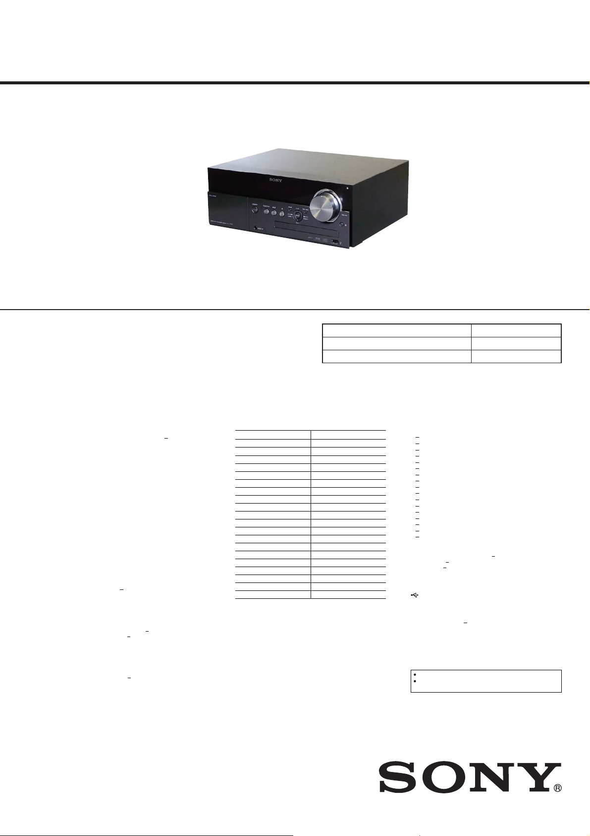
HCD-MX500i/MX550i
SERVICE MANUAL
Canadian Model
Chinese Model
Ver. 1.0 2010.05
Singapore Model
Photo: HCD-MX550i
• HCD-MX500i is the amplifi er, CD player, tuner, USB (Except Canadian) and iPod/iPhone section in CMT-MX500i.
• HCD-MX550i is the amplifi er, CD player, tuner, USB and iPod/iPhone section in CMT-MX550i.
• iPod is a trademark of Apple Inc.
• iPhone is a trademark of Apple Inc.
• MPEG Layer-3 audio coding technology and patents licensed from Fraunhofer IIS and Thomson.
• Windows Media is either a registered trademark or trademark of Microsoft Corporation in the
United States and/or other countries.
• This product is protected by certain intellectual property rights of Microsoft Corporation. Use or
distribution of such technology outside of this product is prohibited without a license from Microsoft or an authorized Microsoft subsidiary.
• All other trademarks and registered trademarks are of their respective holders. In this manual, ™
and ® marks are not specifi ed.
Model Name Using Similar Mechanism NEW
CD Mechanism Type CDM85CD-DVBU102
Optical Pick-up Block Name KHM-313CAA
HCD-MX500i
AEP Model
HCD-MX500i/MX550i
UK Model
HCD-MX550i
Main unit
AUDIO POWER SPECIFICATIONS
With 6 ohm loads, both channels driven, from 120
per channel minimum RMS power, with no more than 10% total harmonic
distortion from 250 milliwatts to rated output.
Amplier section
European model:
DIN power output (rated): 25 watts + 25 watts (6 ohms at 1 kHz, DIN)
Continuous RMS power output (reference): 30 watts + 30 watts (6 ohms at
1 kHz, 10% THD)
Music power output (reference): 30 watts + 30 watts (6 ohms at 1 kHz, 10%
THD)
Other models:
DIN power output (rated): 25 watts + 25 watts (6 ohms at 1 kHz, DIN)
Continuous RMS power output (reference): 30 watts + 30 watts (6 ohms at
1 kHz, 10% THD)
Input
AUDIO IN (stereo mini jack): Sensitivity 700 mV, impedance 47 kilohms
Outputs
SPEAKERS: Accepts impedance of 6 ohms
CD player section
System: Compact disc and digital audio system
Laser Diode Properties
Emission Duration: Continuous
Laser Output*: Less than 44.6μW
* is output is the value measurement at a distance of 200mm from the
objective lens surface on the Optical Pick-up Block with 7mm aperture.
Frequency response: 20 Hz 20 kHz
Signal-to-noise ratio: More than 90 dB
Dynamic range: More than 90 dB
Tuner section
FM tuner section:
FM stereo, FM superheterodyne tuner
Tuning range:
North American model: 87.5 MHz
Other models: 87.5 MHz
Antenna: FM lead antenna
Antenna terminals: 75 ohms unbalanced
Intermediate frequency: 10.7 MHz
DAB/DAB+ tuner section (MX550i only):
FM stereo, DAB/FM superheterodyne tuner
Frequency range*
Band-III: 174.928 (5A) MHz
* For details, see “DAB/DAB+ frequency table” below.
Antenna: DAB/FM lead antenna
Antenna terminal: 75 ohms, F female
108.0 MHz (50 kHz step)
239.200 (13F) MHz
10,000 Hz; rated 30 watts
108.0 MHz (100 kHz step)
SPECIFICATIONS
DAB/DAB+ frequency table (Band-III)
Frequency Label Frequency Label
174.928 MHz 5A 209.936 MHz 10A
176.640 MHz 5B 211.648 MHz 10B
178.352 MHz 5C 213.360 MHz 10C
180.064 MHz 5D 215.072 MHz 10D
181.936 MHz 6A 216.928 MHz 11A
183.648 MHz 6B 218.640 MHz 11B
185.360 MHz 6C 220.352 MHz 11C
187.072 MHz 6D 222.064 MHz 11D
188.928 MHz 7A 223.936 MHz 12A
190.640 MHz 7B 225.648 MHz 12B
192.352 MHz 7C 227.360 MHz 12C
194.064 MHz 7D 229.072 MHz 12D
195.936 MHz 8A 230.784 MHz 13A
197.648 MHz 8B 232.496 MHz 13B
199.360 MHz 8C 234.208 MHz 13C
201.072 MHz 8D 235.776 MHz 13D
202.928 MHz 9A 237.488 MHz 13E
204.640 MHz 9B 239.200 MHz 13F
206.352 MHz 9C
208.064 MHz 9D
* Frequencies are displayed to two decimal places on this system.
iPod/iPhone section
Compatible iPod/iPhone models:
iPod touch 2nd generation
iPod touch 1st generation
iPod classic 120 GB, 160 GB (2009)
iPod classic 160 GB (2007)
iPod classic 80 GB
iPod nano 5th generation (video camera)
iPod nano 4th generation (video)
iPod nano 3rd generation (video)
iPod nano 2nd generation (aluminum)
iPod nano 1st generation
iPod 5th generation (video)
iPod 4th generation (color display)
iPod 4th generation
iPod mini
iPhone
iPhone 3G
iPhone 3GS
USB section (except for North American model)
Supported bit rate:
MP3 (MPEG 1 Audio Layer-3): 32 kbps
WMA: 48 kbps
AAC: 48 kbps
Sampling frequencies:
MP3 (MPEG 1 Audio Layer-3): 32/44.1/48 kHz
WMA: 44.1 kHz
AAC: 44.1 kHz
(USB) port: Type A, maximum current 500 mA
General
Power requirements:
North American model: AC 120 V, 60 Hz
Other models: AC 220 V
Power consumption: 33 watts
Dimensions (W/H/D) (excl. speakers):
Approx. 309 mm × 122 mm × 247 mm
Mass (excl. speakers): Approx. 2.9 kg
Design and specications are subject to change without notice.
Standby power consumption: 0.5 W
Halogenated ame retardants are not used in the certain printed
wiring boards.
192 kbps, VBR
320 kbps
320 kbps, VBR
240 V, 50/60 Hz
9-889-872-01
2010E05-1
2010.05
©
COMPACT DISC RECEIVER
Sony Corporation
Audio&Video Business Group
Published by Sony Techno Create Corporation
HCD-MX500i/MX550i
NOTES ON CHIP COMPONENT REPLACEMENT
• Never reuse a disconnected chip component.
• Notice that the minus side of a tantalum capacitor may be damaged by heat.
FLEXIBLE CIRCUIT BOARD REPAIRING
• Keep the temperature of soldering iron around 270 °C during
repairing.
• Do not touch the soldering iron on the same conductor of the
circuit board (within 3 times).
• Be careful not to apply force on the conductor when soldering
or unsoldering.
Laser component in this product is capable of emitting radiation
exceeding the limit for Class 1.
This appliance is classifi ed as
a CLASS 1 LASER product.
This marking is located on the
rear or bottom exterior.
SAFETY-RELATED COMPONENT WARNING!
COMPONENTS IDENTIFIED BY MARK 0 OR DOTTED LINE
WITH MARK 0 ON THE SCHEMATIC DIAGRAMS AND IN
THE PARTS LIST ARE CRITICAL TO SAFE OPERATION.
REPLACE THESE COMPONENTS WITH SONY PARTS
WHOSE PART NUMBERS APPEAR AS SHOWN IN THIS
MANUAL OR IN SUPPLEMENTS PUBLISHED BY SONY.
ATTENTION AU COMPOSANT AYANT RAPPORT
À LA SÉCURITÉ!
LES COMPOSANTS IDENTIFIÉS PAR UNE MARQUE 0 SUR
LES DIAGRAMMES SCHÉMATIQUES ET LA LISTE DES
PIÈCES SONT CRITIQUES POUR LA SÉCURITÉ DE FONCTIONNEMENT. NE REMPLACER CES COMPOSANTS QUE
PAR DES PIÈCES SONY DONT LES NUMÉROS SONT DONNÉS DANS CE MANUEL OU DANS LES SUPPLÉMENTS
PUBLIÉS PAR SONY.
TABLE OF CONTENTS
1. SERVICING NOTES ............................................. 3
2. DISASSEMBLY
2-1. Disassembly Flow ........................................................... 8
2-2. Case ................................................................................. 8
2-3. Front Panel Block ........................................................... 9
2-4. Knob (VOL) .................................................................... 10
2-5. MAIN Board ................................................................... 10
2-6. SP Board ......................................................................... 11
2-7. POWER Board ................................................................ 11
2-8. CD Block ........................................................................ 12
2-9. BD96/BD96U Board ....................................................... 13
2-10. Belt .................................................................................. 13
2-11. FFC Holder ..................................................................... 14
2-11. Optical Pick-up Block (KHM-313CAA) ........................ 14
3. TEST MODE ............................................................ 15
4. ELECTRICAL CHECK ......................................... 18
5. DIAGRAMS
5-1. Block Diagram - CD, USB Section - .............................. 19
5-2. Block Diagram
- TUNER, iPod/iPhone, AUDIO IN Section - ................ 20
5-3. Block Diagram - OUTPUT, PANEL Section - ............... 21
5-4. Block Diagram - POWER SUPPLY Section - ................ 22
5-5. Printed Wiring Board
- BD96/BD96U Board (Side A) - ................................... 24
5-6. Printed Wiring Board
- BD96/BD96U Board (Side B) - ................................... 25
5-7. Schematic Diagram - BD96/BD96U Board (1/2) - ........ 26
5-8. Schematic Diagram - BD96/BD96U Board (2/2) - ........ 27
5-9. Printed Wiring Board - DAB Board (MX550i) - ............ 28
5-10. Schematic Diagram - DAB Board (MX550i) - ............... 29
5-11. Printed Wiring Board - MAIN Board (1/2) - .................. 30
5-12. Printed Wiring Boards - MAIN Board (2/2) - ................. 31
5-13. Schematic Diagram - MAIN Section (1/4) - ................... 32
5-14. Schematic Diagram - MAIN Section (2/4) - ................... 33
5-15. Schematic Diagram - MAIN Section (3/4) - ................... 34
5-16. Schematic Diagram - MAIN Section (4/4) - ................... 35
5-17. Printed Wiring Boards - IP/JACK/SP/USB Boards - ..... 36
5-18. Schematic Diagram - IP/JACK/SP/USB Boards - .......... 37
5-19. Printed Wiring Boards - PANEL Section - ..................... 38
5-20. Schematic Diagram - PANEL Section - .......................... 39
5-21. Printed Wiring Board - POWER Board - ........................ 40
5-22. Schematic Diagram - POWER Board - .......................... 41
6. EXPLODED VIEWS
6-1. Case Section .................................................................... 54
6-2. Front Panel Section ......................................................... 55
6-3. iPod Dock Section .......................................................... 56
6-4. MAIN Board Section ...................................................... 57
6-5. Chassis Section ............................................................... 58
6-6. CD Mechanism Deck Section
(CDM85CD-DVBU102) ................................................ 59
7. ELECTRICAL PARTS LIST .............................. 60
2
SECTION 1
SERVICING NOTES
HCD-MX500i/MX550i
NOTES ON HANDLING THE OPTICAL PICK-UP
BLOCK OR BASE UNIT
The laser diode in the optical pick-up block may suffer electrostatic break-down because of the potential difference generated by
the charged electrostatic load, etc. on clothing and the human body.
During repair, pay attention to electrostatic break-down and also
use the procedure in the printed matter which is included in the
repair parts.
The fl exible board is easily damaged and should be handled with
care.
NOTES ON LASER DIODE EMISSION CHECK
The laser beam on this model is concentrated so as to be focused
on the disc refl ective surface by the objective lens in the optical
pickup block. Therefore, when checking the laser diode emission,
observe from more than 30 cm away from the objective lens.
UNLEADED SOLDER
Boards requiring use of unleaded solder are printed with the leadfree mark (LF) indicating the solder contains no lead.
(Caution: Some printed circuit boards may not come printed with
the lead free mark due to their particular size)
: LEAD FREE MARK
Unleaded solder has the following characteristics.
• Unleaded solder melts at a temperature about 40 °C higher
than ordinary solder.
Ordinary soldering irons can be used but the iron tip has to be
applied to the solder joint for a slightly longer time.
Soldering irons using a temperature regulator should be set to
about 350 °C.
Caution: The printed pattern (copper foil) may peel away if
the heated tip is applied for too long, so be careful!
• Strong viscosity
Unleaded solder is more viscous (sticky, less prone to fl ow)
than ordinary solder so use caution not to let solder bridges
occur such as on IC pins, etc.
• Usable with ordinary solder
It is best to use only unleaded solder but unleaded solder may
also be added to ordinary solder.
NOTE OF REPLACING THE MS-203 BOARD
When the MS-203 board is damaged, exchange the entire
CDM85 (CD) ASSY.
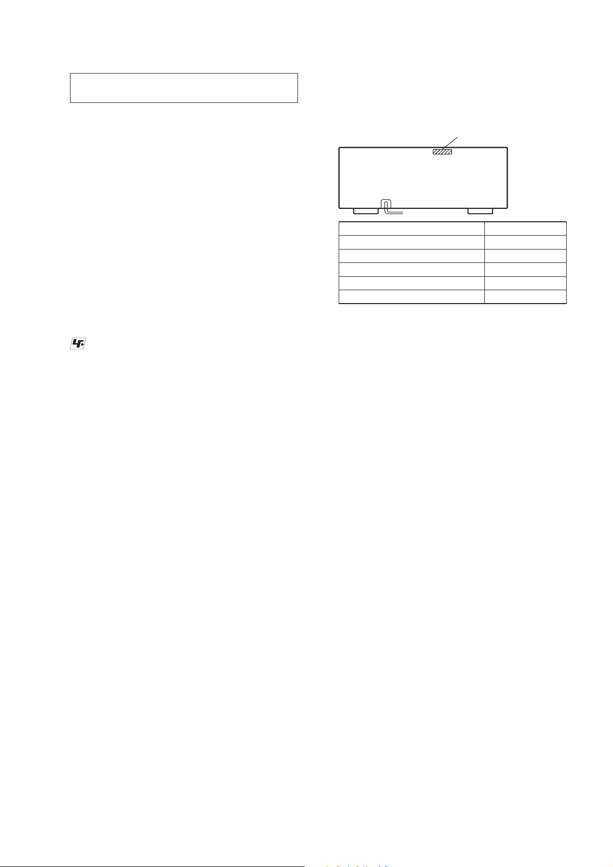
MODEL IDENTIFICATION
– Back Panel –
Model Part No.
HCD-MX500i: AEP model
HCD-MX500i: Canadian model
HCD-MX500i: Singapore model
HCD-MX500i: Chinese model
HCD-MX550i: AEP, UK models
PART No.
4-175-955-0[]
4-175-955-2[]
4-175-955-3[]
4-175-955-4[]
4-175-955-5[]
RELEASING THE ANTITHEFT LOCK
The disc tray lock function for the antitheft of an demonstration
disc in the store is equipped.
Releasing Procedure:
1. Press the [
] button to turn the power on.
?/1
2. While pressing the [x] button, press the [Z] button unit “UNLOCKED” displayed on the fl uorescent indicator tube (around
5 seconds) .
Note: When “LOCKED”is displayed, the disc tray lock is not released by
turning power on/off with the [
?/1
] button.
3
HCD-MX500i/MX550i
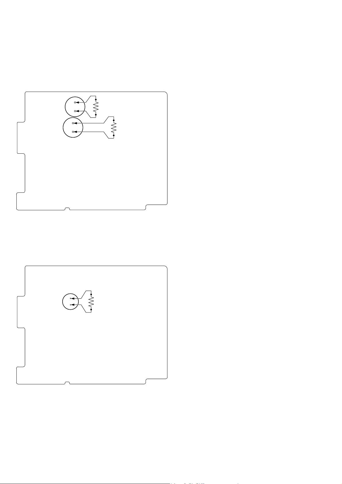
CAPACITOR ELECTRICAL DISCHARGE PROCESSING
When checking the board, the electrical discharge is necessary for the electric shock prevention.
Connect the resistors referring to the fi gure below.
• POWER board (C11, C12) (Canadian model)
Both ends of respective capacitors.
– POWER Board (Conductor Side) –
C12
C11
• POWER board (C10) (Except Canadian model)
Both ends of respective capacitors.
– POWER Board (Conductor Side) –
800 :/2 W
800 :/2 W
C10
800 :/2 W
4
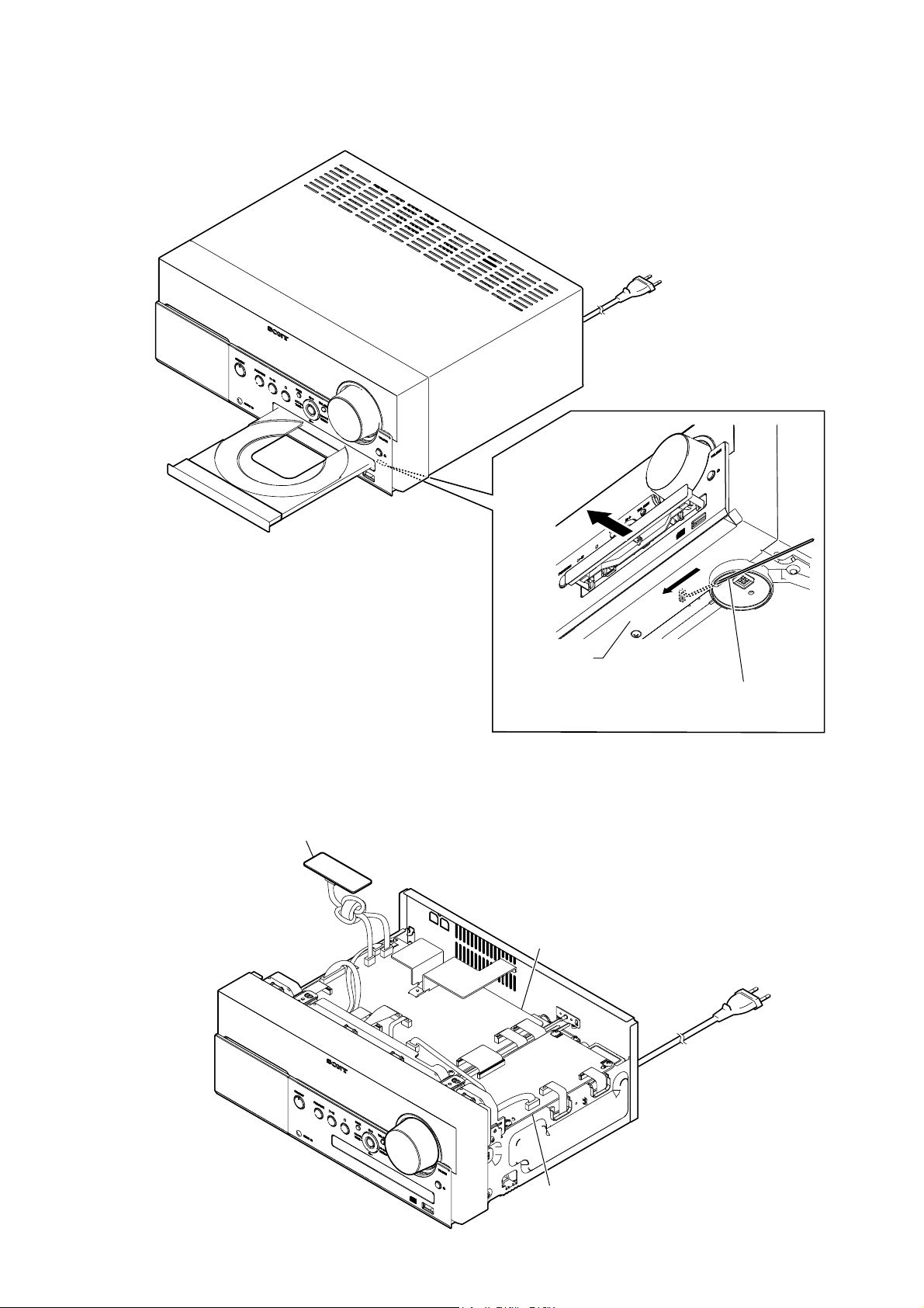
HOW TO OPEN THE TRAY WHEN POWER SWITCH TURN OFF
HCD-MX500i/MX550i
1 Insert the hard metal fittings of L character type in the
hole of the chassis, and push the lever in the direction
of the arrow.
MAIN, BD96/BD96U AND SP BOARDS SERVICE POSITION
SP board
bottom side
MAIN board
BD96 board (Canadian)
BD96U board (Except Canadian)
5
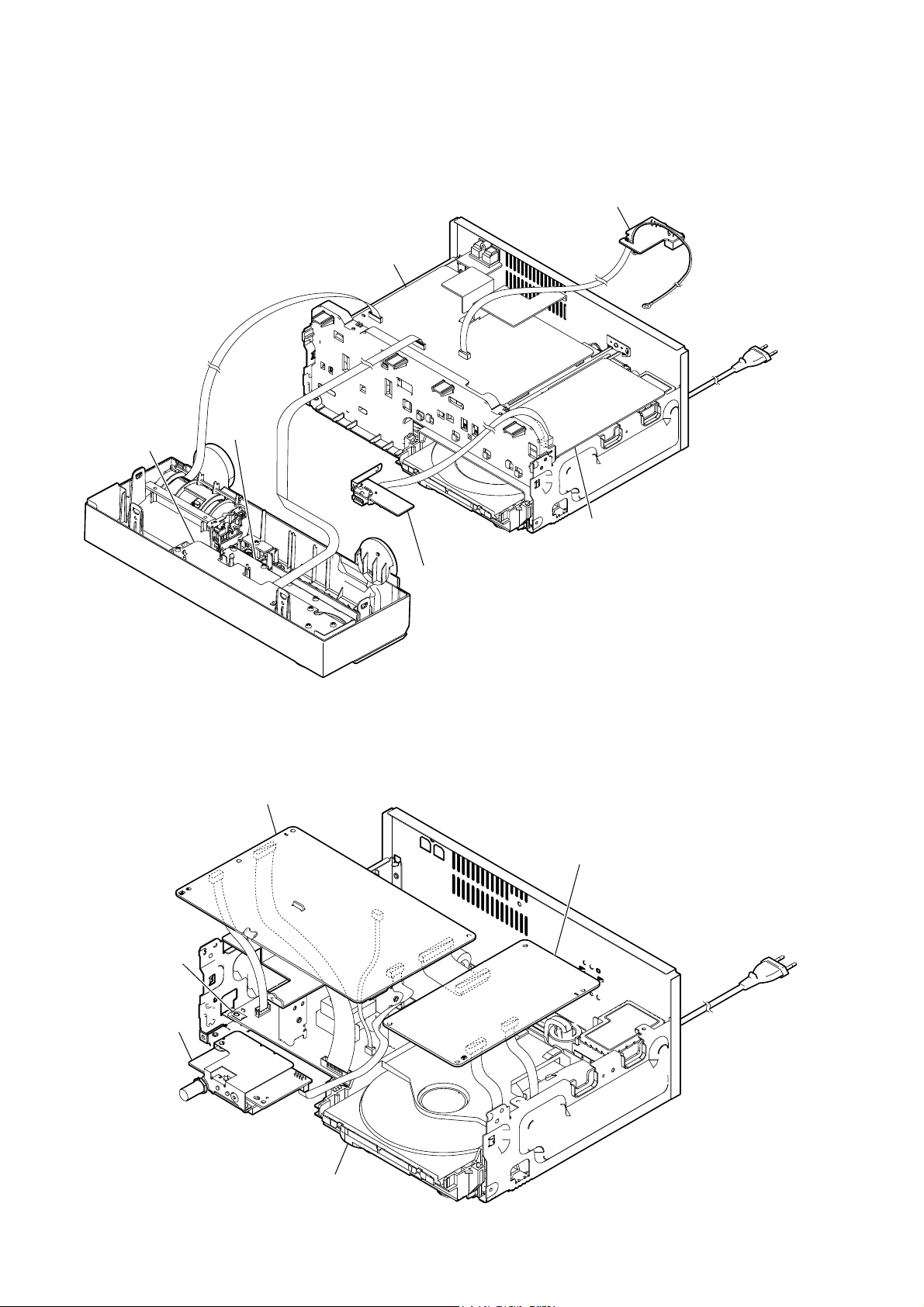
HCD-MX500i/MX550i
FL, KEY, JACK AND USB BOARDS SERVICE POSITION
MAIN board
JACK board
FL board
KEY board
BD96 board (Canadian)
BD96U board (Except Canadian)
USB board (Except Canadian)
CD MECHANISM DECK, MAIN AND BD96/BD96U BOARDS SERVICE POSITION
MAIN board
BD96 board (Canadian)
BD96U board (Except Canadian)
POWER board
DAB board (MX550i)
6
CD mechanism deck
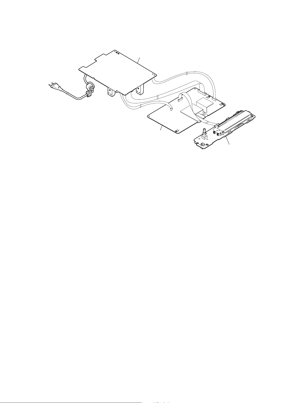
POWER BOARD SERVICE POSITION
HCD-MX500i/MX550i
POWER board
MAIN board
FL board
7
HCD-MX500i/MX550i
DISASSEMBLY
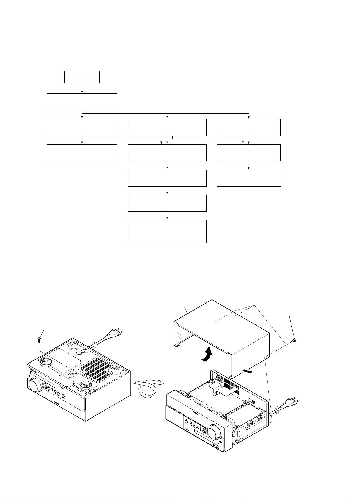
• This set can be disassembled in the order shown below.
2-1. DISASSEMBLY FLOW
SET
2-2. CASE
(Page 8)
SECTION 2
2-3. FRONT PANEL BLOCK
(Page 9)
2-4. KNOB (VOL)
(Page 10)
Note: Follow the disassembly procedure in the numerical order given.
2-5. MAIN BOARD
(Page10)
2-8. CD BLOCK
(Page 12)
2-9. BD96/BD96U BOARD
(Page 13)
2-11. FFC HOLDER
(Page 14)
2-12. OPTICAL PICK-UP BLOCK
(KHM-313CAA)
(Page 14)
2-2. CASE
2-6. SP BOARD
(Page 11)
2-7. POWER BOARD
(Page 11)
2-10. BELT
(Page 13)
1 two screws
(BV/RING)
– Bottom view –
5 case
3
2 three screws
(BV/RING)
4
3
8
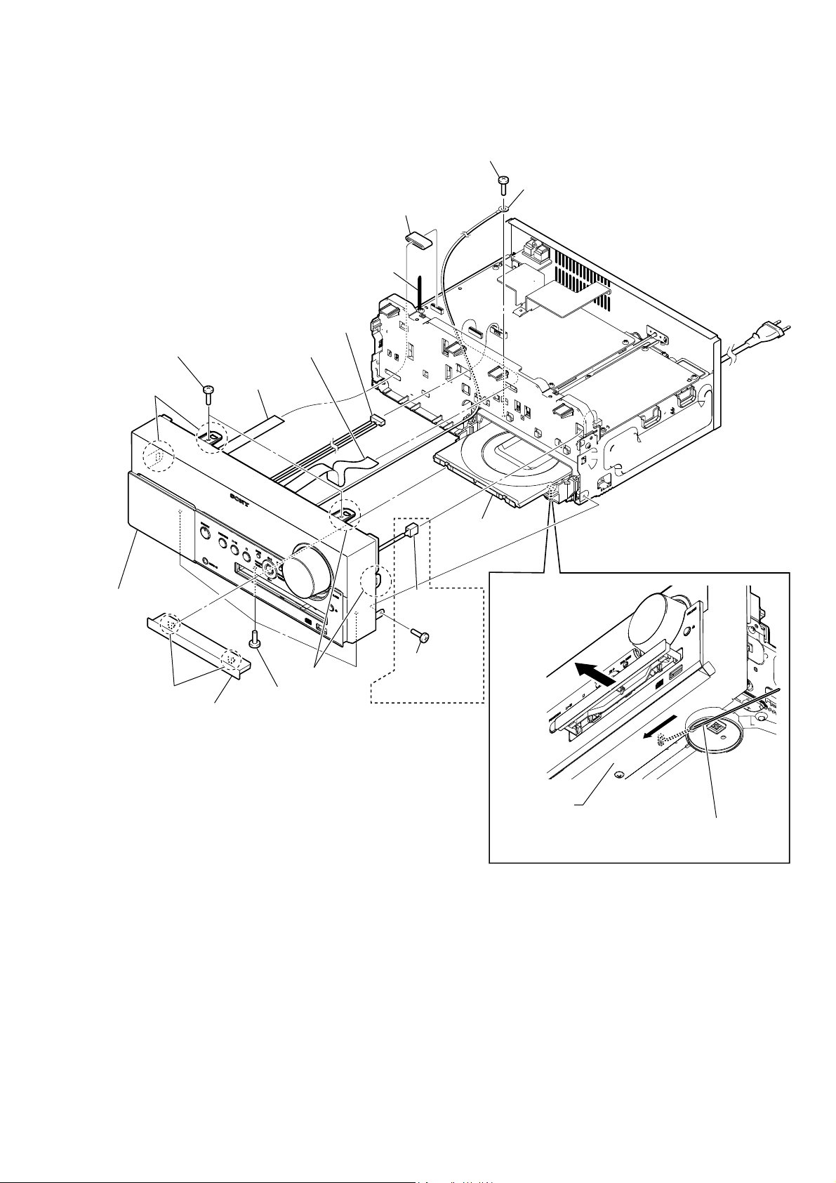
2-3. FRONT PANEL BLOCK
5 Lift up the coating clip.
8 flexible flat cable
qs two screws
(BV3)
qg two claws
(13 core) (CN404)
6 flexible flat cable
(13 core) (CN409)
7 ferrite core
9 connector
(CN402)
qd screw (BV3)
HCD-MX500i/MX550i
lead wire (from HP board)
qf
qh front panel block
3 two claws
4 panel (CD) block
qg two claws
qs three screws
(BV3)
2 Draw out
the tray.
0 connector
(CN402)
qa screw
(BV3)
(EXCEPT Canadian)
bottom side
1 Insert the hard metal fittings of L character type in the
hole of the chassis, and push the lever in the direction
of the arrow.
9
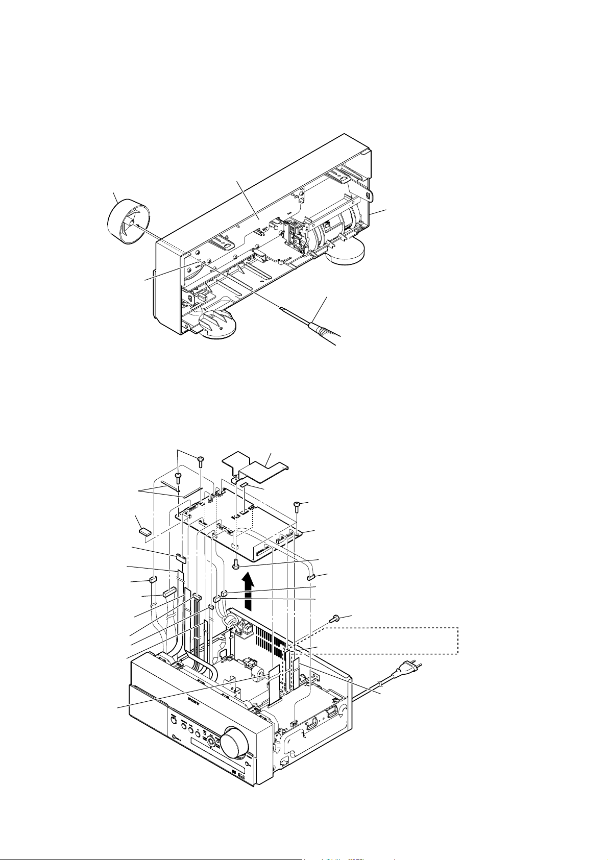
HCD-MX500i/MX550i
2-4. KNOB (VOL)
Note: The illustration sees the front panel block from FL board side.
knob (VOL)
2
2-5. MAIN BOARD
hole
FL board
qg two screws (BV3)
Push the knob (VOL) by flat-head screwdriver.
1
ql heatsink (AMP)
front panel block
qh two coating clips
wa cushion (ferrite)
2 ferrite core
1 flexible flat cable
(13 core) (CN409)
3 connector (CN704)
4 connector (CN412)
5 flexible flat cable
(13 core) (CN404)
6 connector (CN402)
7 connector (CN417)
8 flexible flat cable
(5 core) (CN410)
9 flexible flat cable
(19 core) (CN408)
(Canadian)/
flexible flat cable
(27 core) (CN415)
(Except Canadian)
qj
w; radiation sheet
qg three screws (BV3)
ws MAIN board
qk two screws (BV3)
qs connector (CN401)
qd connector (CN703)
qf connector (CN702)
qg screw (BV3)
(MX550i)
qa flexible flat cable (9 core) (CN407)
0 flexible flat cable (9 core) (CN405)
(CND, CH, SP)/
flexible flat cable (11 core) (CN406)
(AEP, UK)
• Abbreviation
CH : Chinese model
CND : Canadian model
SP : Singapore model
10
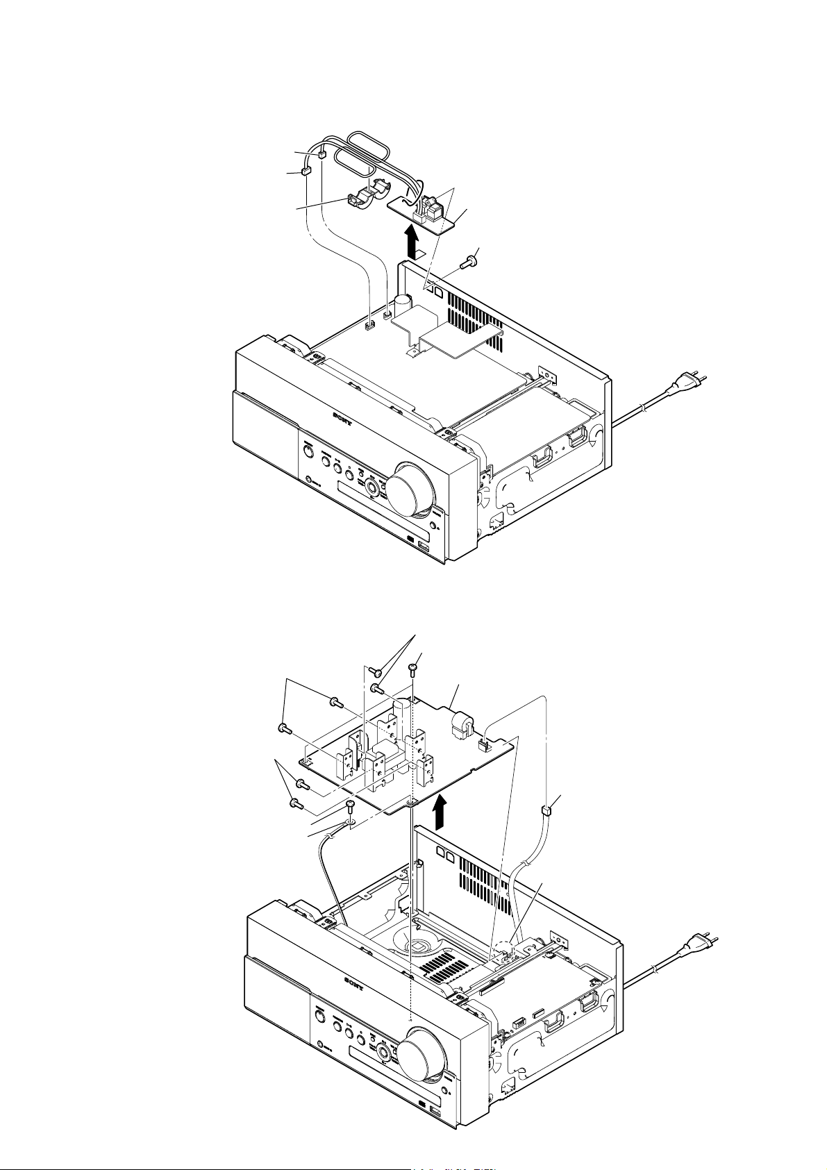
2-6. SP BOARD
2 connector (CN703)
1 connector (CN702)
HCD-MX500i/MX550i
5 clamp filter
2-7. POWER BOARD
4
6 SP board
3 screw (BV3)
6 two screws (BV3)
6 two screws (BV3)
2 screw (BV3)
lead wire (from HP board)
3
6 two screws (BV3)
2 two screws (BV3)
7 POWER board
5
1 power cord connector
(CN1)
4 claw
11
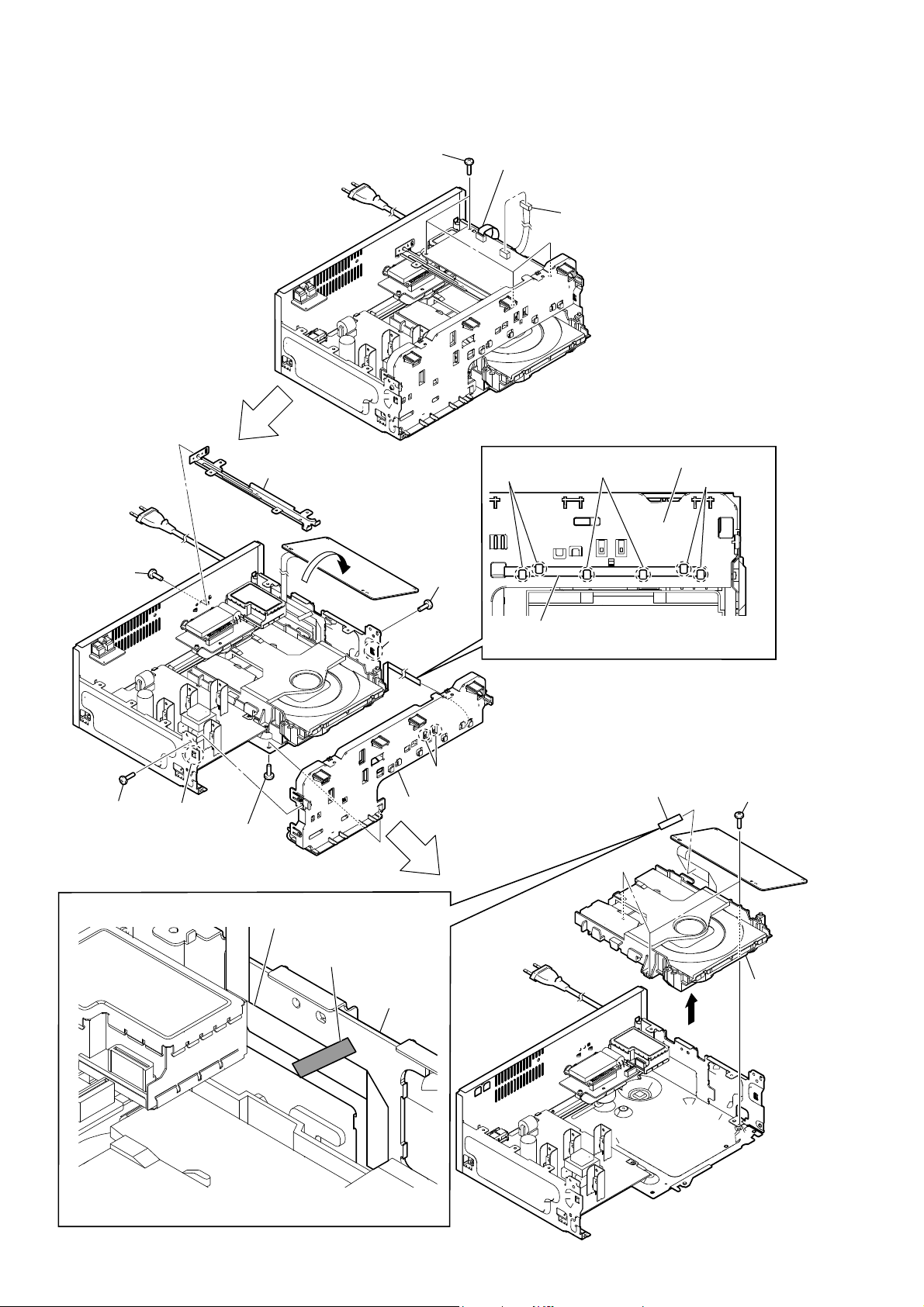
HCD-MX500i/MX550i
2-8. CD BLOCK
4 screw (BV3)
2 four screws (BV3)
6 bracket (center)
3
8 screw
(BV3)
Note 1: Do not remove this connector (CN201) at this point.
It is necessary to process electrostatic measures of
optical pick-up.
1 connector (CN301)
7 two claws
7 two claws
bracket (front)
7 two claws
8 screw (BV3)
9 claw
8 screw (BV3)
wire (flat type) (24 core)
filament tape
guard board
9 claw
5 two claws
0 bracket (front)
flexible flat cable (5 core)
– Front side view –
qa filament tape
qs three screws
(BV3)
qf CD block
qd
Note 2: When you install CD block, fix the wire (flat type) (24 core) with
the filament tape firmly as shown in figure.
12
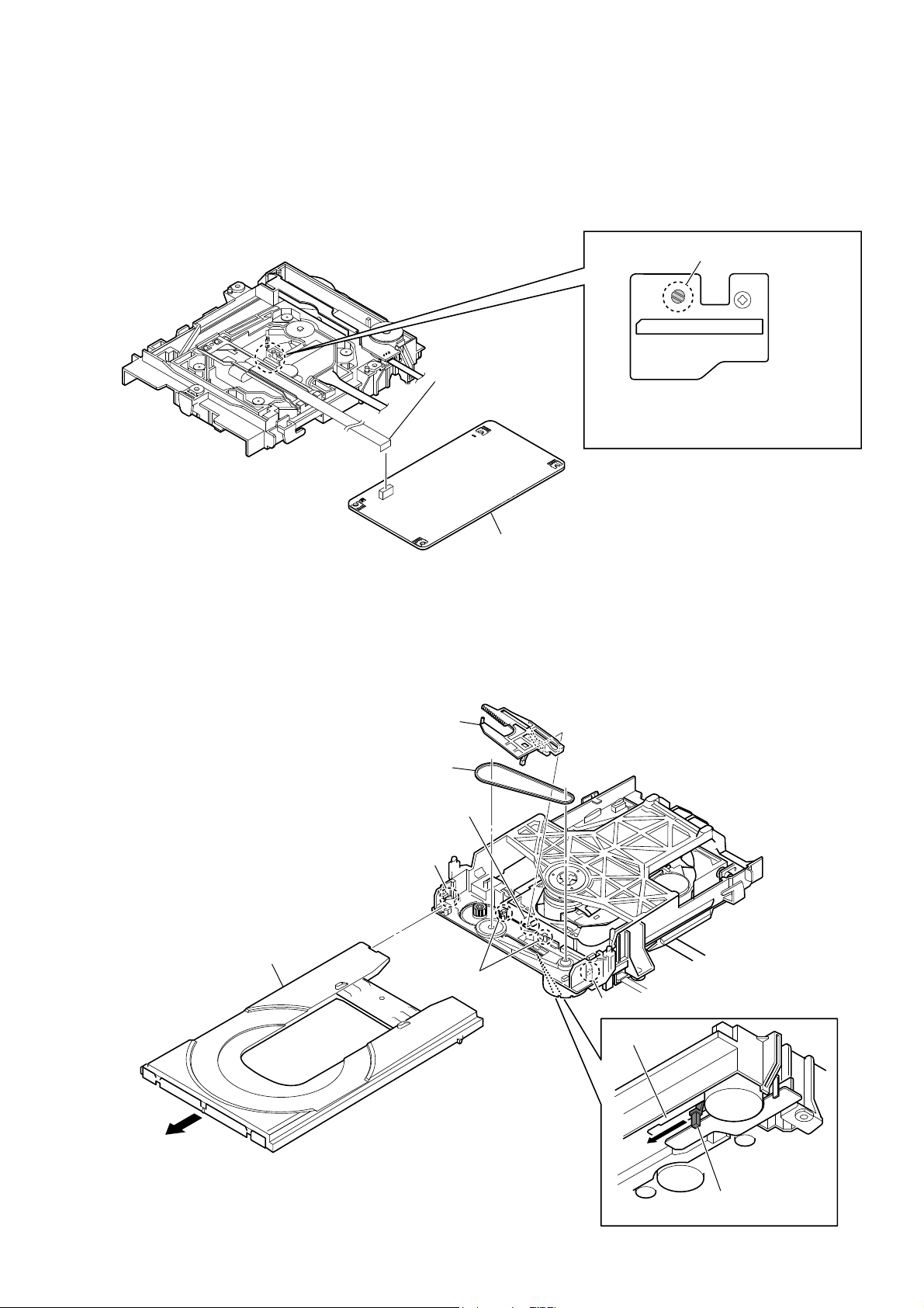
2-9. BD96/BD96U BOARD
Note 1: When disconnection the wire (fl at type) (24 core) of optical pick-up block, solder the short-land.
2 wire (flat type) (24 core)
(CN201)
Note 2: When assembling the optical pick-up block,
remove the solder of short-land after
connecting the wire (flat type) (24 core).
– CD mechanism deck block bottom view –
HCD-MX500i/MX550i
Solder the short-land.
1
• Abbreviation
CH : Chinese model
CND : Canadian model
SP : Singapore model
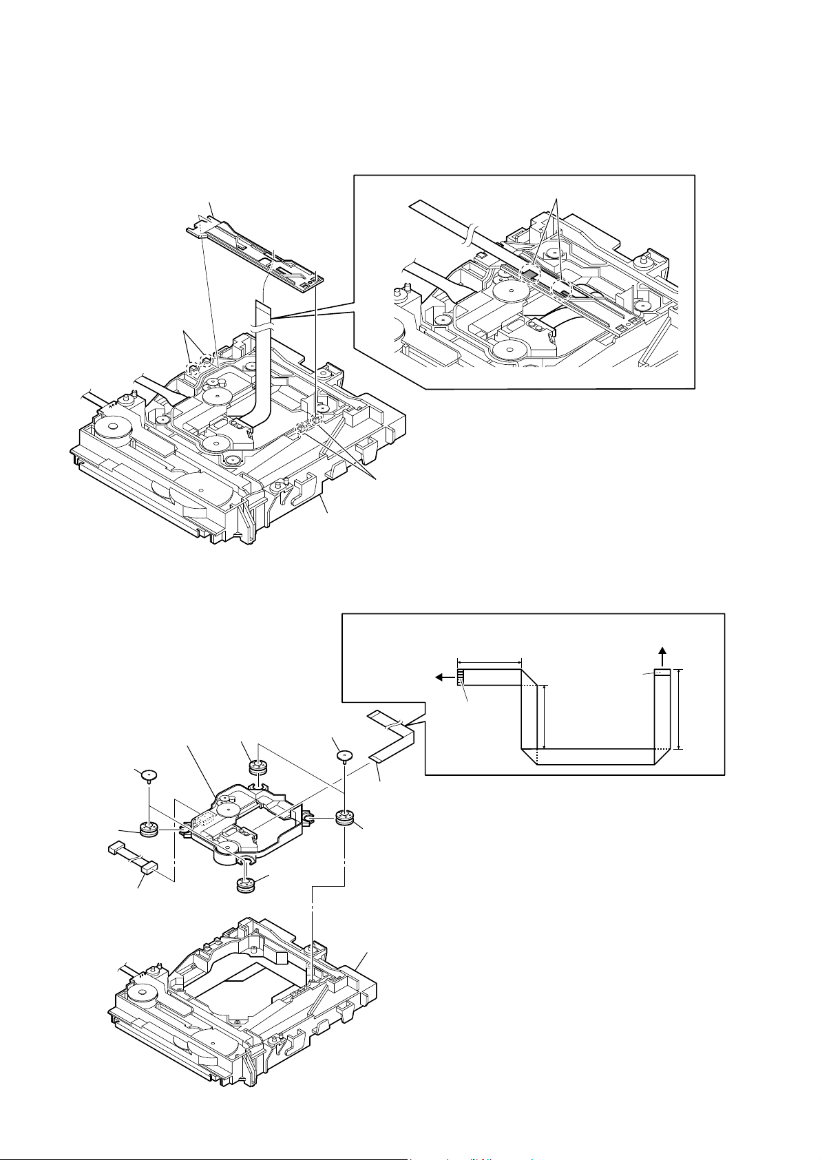
2-10. BELT
3 BD96 board (MX500i: CND)/
BD96U board (MX500i: AEP, CH, SP/MX550i)
7 chuck cam
8 belt
6 shaft
3 claw
4 tray
5 two hooks
2
3 claw
bottom side
1 Push the lever in the
direction of the arrow.
13
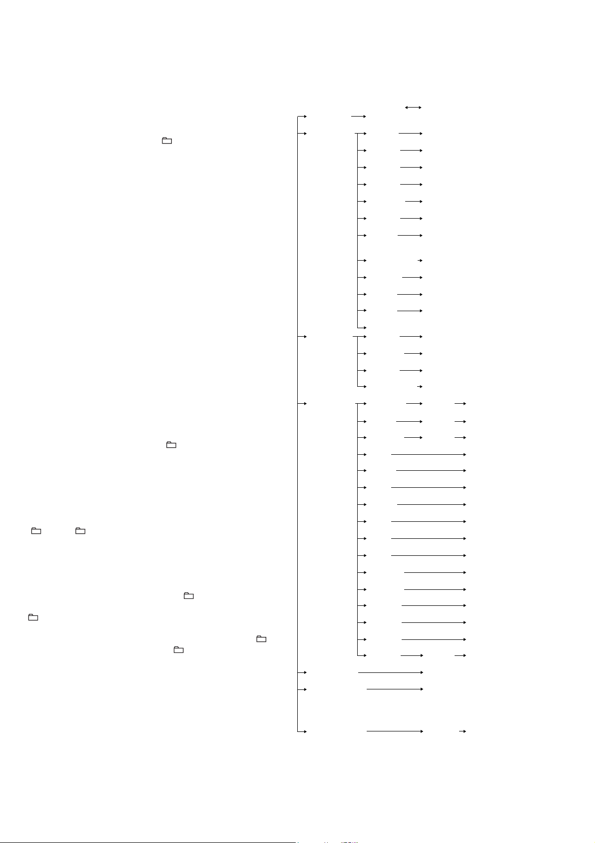
HCD-MX500i/MX550i
2-11. FFC HOLDER
Note 1: The illustration sees the CD mechanism deck block from optical pick-up block side.
3 FFC holder
Note 2: Remove the FFC holder from the
original set and install it again.
1 two claws
2 two claws
CD mechanism deck block
2-12. OPTICAL PICK-UP BLOCK (KHM-313CAA)
+RZWREHQGWKHwire (flat type) (24 core)
two screws
optical pick-up block
6
(KHM-313CAA)
two screws
1
(PTPWH M2.6)
insulator
3
connector
5
insulator
3
1
(PTPWH M2.6)
insulator
3
1 two claws
to BD96/BD96U
board (CN201)
wire (flat type) (24 core)
4
insulator
3
40 mm
The upper side
is contact side.
The lower side
is contact side.
40 mm
to optical pick-up block
(KHM-313CAA)
50 mm
14
– CD mechanism deck block bottom view –
mechanism deck
2
(CDM85 (CD))

SECTION 3
TEST MODE
HCD-MX500i/MX550i
COLD RESET
The cold reset clears all data including preset data stored in the
memory to initial conditions. Execute this mode when returning
the set to the customer.
Procedure:
1. In the standby status, press the [?/1] button to turn the power
on.
2. Press two buttons of [ENTER] and [
3. When “RESET” appears, the set enters.
AUTO STANDBY MODE
This mode is used to change the automatic standby function.
With this function, the system enters standby mode automatically
in about 30 minutes when there is no operation or audio signal
output.By default, the automatic standby function is turned on.
Procedure:
1. Press the [
2. Press the [
3. The message “AUTO STBY” → “OFF” is displayed on the
fl uorescent indicator tube and the automatic standby OFF
mode is set.
4. To turn this function on, press the [
onds.
The message “AUTO STBY” → “ON” is displayed on the
fl uorescent indicator tube and the automatic standby ON mode
is set.
COMMON TEST MODE
This mode is used to check operations of amplifi er.
Procedure:
1. Press the [?/1] button to turn the power on.
2. Press two buttons of [ENTER] and [FUNCTION] simultaneously.
3. When the COMMON test mode is activated, “AUDIO IN”
is displayed on the fl uorescent indicator tube and “c PLAY
SLEEP” blink on the fl uorescent indicator tube.
4. Each time [EQ] button on the remote commander is pressed,
the display changes starting “TONE MAX”, “TONE MIN”
and “TONE FLAT” this order.
5. Turn the [VOLUME] knob counterclockwise, “VOLUME
MIN” is displayed on the fl uorescent indicator tube. Turn the
[VOLUME] knob clockwise, “VOLUME MAX” is displayed
on the fl uorescent indicator tube.
6. To release this mode, press the [?/1] button.
PANEL TEST MODE
This mode is used to check the fl uorescent indicator tube, LED,
model, destination, software version and key.
Procedure:
1. Press the [?/1] button to turn the power on.
2. Press three buttons of [ENTER] and [x] simultaneously.
3. All segments on the fl uorescent indicator tube, [STANDBY]
LED light up.
4. Press the [ENTER] button, the model and destination are displayed on the fl uorescent indicator tube.
5. Press the [ENTER] button again, MC version is displayed on
the fl uorescent indicator tube.
6. Each time [ENTER] button is pressed, the display changes
starting from MC version, GC version, USBL version , USBM
version, IPL version, CD version, CDD version, CDMA version, CDMB version, BDA version, BDB version, ST version,
TA version and TM version this order, and returns to the MC
version display.
7. When [x] button is pressed while the MC version is displayed,
year, month and day of the software creation is displayed.
When [
MC version display.
] button to turn the power on.
?/1
] button for 2 seconds.
?/1
] button is pressed again, the display returns to the
x
] simultaneously.
?/1
] button again for 2 sec-
?/1
8. Press the [TOOL MENU] button, the key test mode is activated and “K 0 V0” is displayed on the fl uorescent indicator
tube.
9. Each time a button is pressed, “K” value increases. However,
once a button is pressed, it is no longer taken into account.
All keys are pressed, display becomes “K9” .
10. “V” value increases 2, 4, 6 ... if turn the [VOLUME] knob
clockwise, or it decreases 8, 6, 4 ... if turn the knob counterclockwise.
11. To release this mode, press three buttons in the same manner as
step 2, or disconnect the power cord.
CD SHIP MODE
This mode moves the optical pick-up to the position durable to
vibration. Use this mode when returning the set to the customer
after repair.
Procedure:
1. Press the [
2. Press the [FUNCTION] button to select “CD”.
3. Press two buttons of [TOOL MENU] and [?/1] simultaneously.
4. After blink “STANDBY”, “LOOK” is displayed, disconnect
the AC plug.
CD SHIP MODE & MEMORY CLEAR
This mode is used to perform CD ship mode and cold reset simultaneously.
Procedure:
1. Press the [?/1] button to turn the power on.
2. Press three buttons of [x] and [DSGX] simultaneously.
3. After blink “STANDBY”, “LOOK” is displayed disconnect
the AC plug.
ANTITHEFT LOCK MODE
This mode is used to unable to take sample disc out of disc tray in
the shop.
Procedure:
1. Press the [?/1] button to turn the power on.
2. Press the [Z] button to open the disc tray and set the CD disc.
3. Press the [Z] button to close the disc tray.
4. Press two buttons of [
5. The message “LOCKED” is displayed on the fl uorescent indi-
cator tube and the disc tray is locked. (Even if pressing the [
button, the message “LOCKED” is displayed on the fl uores-
cent indicator tube and the disc tray is locked)
6. To release from this mode, press two buttons of [
for 5 seconds.
7. The message “UNLOCKED” is displayed on the fl uorescent
indicator tube and the disc tray is unlocked.
CD POWER MANAGE
This mode is used to changed over CD power on/off for decreasing
of reception noise in the tuner mode.
Procedure:
1. Press the [?/1] button to turn the power on.
2. Press the [FUNCTION] button to select “CD”.
3. Press the [?/1] button again to turn the power off.
4. Press two buttons of [ + v] and [?/1] simultaneously.
5. The message “CD POWER ON” or “CD POWER OFF” is displayed on the fl uorescent indicator tube, and CD power on/off
is changed over in the tuner mode.
] button to turn the power on.
?/1
] and [Z] for 5 seconds.
x
] and [Z]
x
Z
]
15
HCD-MX500i/MX550i
CD SERVICE MODE
This mode can run the CD sled motor freely. Use this mode, for
instance, when cleaning the optical pick-up.
Procedure:
1. Press the [?/1] button to turn the power on.
2. Press the [FUNCTION] button to select “CD”.
3. Press three buttons of [x] and [ + v] simultaneously, the
message “SERVICE MO” is displayed on the fl uorescent indi-
cator tube.
4. Press the [
l m
up to inside track and the message “SLED IN” is displayed on
the fl uorescent indicator tube, or press the [
+] button to outside track and the message “SLED OUT” is
displayed on the fl uorescent indicator tube.
5. Press the [u] button, “LD ON” or “LD OFF” is displayed
on the fl uorescent indicator tube. Each time [u] button is
pressed, laser diode on/off is changed over.
6. To release this mode, press the [
CD SERVO TEST MODE
This mode can check the servo system operations of the optical
pick-up system (= optical unit + BD96/BD96U board).
Note 1: Do not enter the [CD SERVO TEST MODE] while any other test
mode is in progress.
Note 2: Do not enter any other test mode while the [CD SERVO TEST
MODE] is in progress.
Note 3: In RAM Read, “SBADrough”, “SBBTrough”, “DT-GI roug”,
“SBAD fi ne”, “SBBT fi ne”, “DT-GI fi ne”, “DSPcomcnt”, and
“EDCcomcnt” are displayed but are not used in the service.
How to Enter the CD Servo Test Mode
Procedure:
1. Press the [
?/1
2. Press the [FUNCTION] button to select CD function.
3. Press three buttons of [
4. It enters the CD servo test mode and displays “bdt S CURV”.
How to Exit from the CD Servo Test Mode
Procedure:
1. To release this mode, press the [
Key Operation:
+ v], [V –]:
[
Use these keys to move between the seven modes contained in the
CD Servo Test Mode, that are the S-Curve Mode, the RAM Read
Mode, the RAM Write Mode, the Command Out Mode, the Error
Rate Mode the LOG Initialize Mode and the LOG Read Mode as
described below. Also, use these keys to move between the menus
within the respective seven modes. When [ + v] is pressed, the
screen advances to the next menu or to the next mode. When [V
–] is pressed, the screen returns back to the previous menu or
to the previous mode. Use these keys also to increase or decrease
the numeric value when changing the numeric value. Pressing [
+ v] increases the value and pressing [V –] decreases the value.
[ENTER], [
]:
x
Use these keys to move between the different layers of the hierarchy of the CD Servo Test Mode shown below. Press [ENTER]
to move down to the lower layer, and press [x] to move up to the
higher layer.
[
M L
TUNE +], [
Use these keys to move the cursor to the right digit or to the left
digit in the six-digit number, when changing the numeric value.
M L
Press [
press [
l m
TUNE –] button to move the optical pick-
TUNE
?/1
M L
] button.
] button to turn the power on.
], and [
x
l m
TUNE –]:
] simultaneously.
V ‒
] button.
?/1
TUNE +] to move the cursor to the right, and
TUNE –] to return the cursor to the left.
[
]:
u
Use this key to execute Command Out in the Command Out Mode.
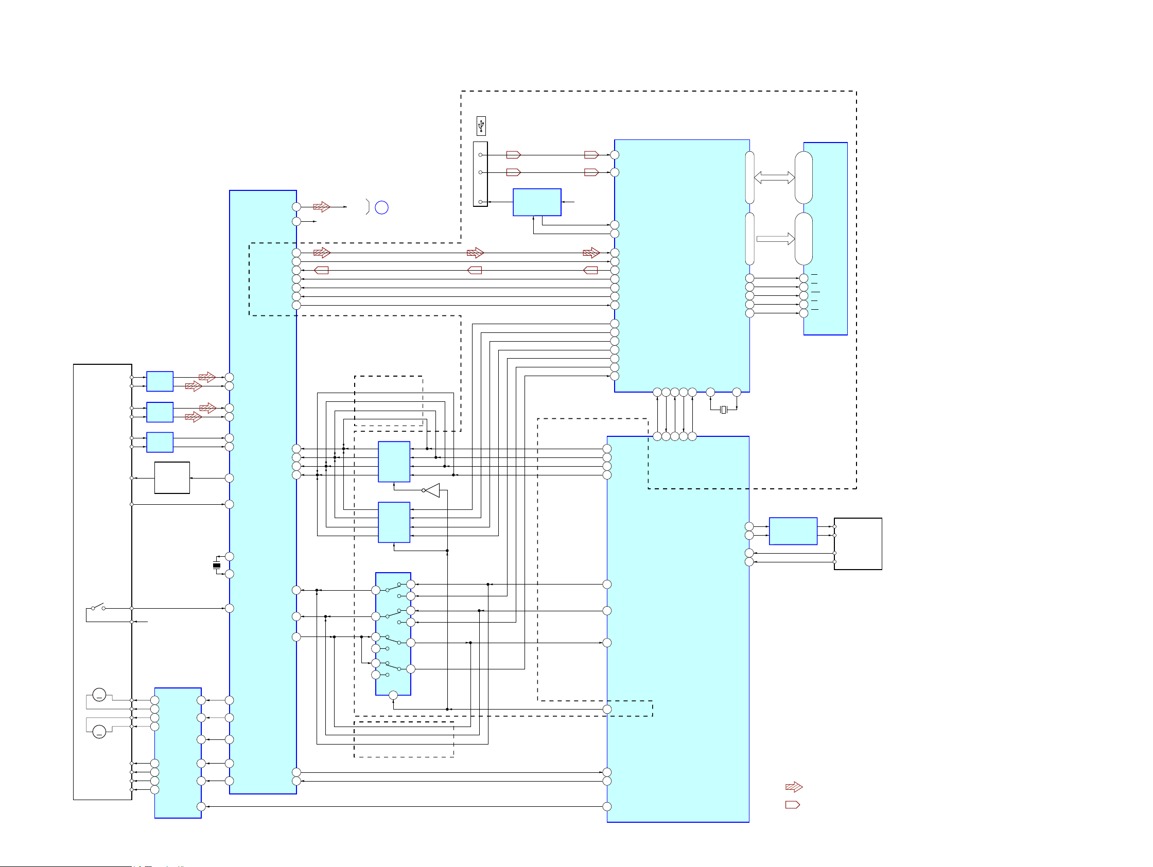
CD Servo Test Mode Tree:
S Curve Mode LD ON
(bdt S CURV) (LD ON)
RAM Read Mode
(bdtRAM REA) (DiscType) (AL: 0000, RW: 0001)
Gain Index value indication
(GainIndx) (0001)
RFO GAIN value indication
(RFO_GAIN) (0008)
FEO GAIN value indication
(FEO_GAIN) (0005)
SBAD GAIN value indication
(SBAD_GAIN) (0008)
TEO GAIN value indication
(TEO_GAIN) (0008)
Disc Size value indication
(DiscSize) (0000: Non disc, 0001: 8cm,
0002: 12cm)
(OpAbrkErr) (0000)
SBBT Data value indication
(SBBT Data) (0053)
TE Peak value indication
(TE P-P) (0097)
FEOOCD value indication
(FEOOCD) (00C0)
The following items are not used (Note 3)
RAM Write Mode
(bdtRAM WRI) (00 SPG_M) (Non mask:00, Mask:01)
Fix RF Gain value edit
(00 FixRF) (Non Fix:00, AL Fix:01, RW Fix:02)
TMAX ON value edit
(00 tmaxo)
Driver Mute OFF value edit
(00 d_mut) (Normal:00, Forced OFF:01)
Command Out Mode
(bdt COMOUT) (COMOUT6X) (000000) (OK)
READ2X value edit command out
(READ2X) (60) (50)
REG READ value edit command out
(REG_READ) (00) (0000)
FEBC? command out
(FEBC?) (00)
FGADD? command out
(FGADD?) (FA)
TEBC? command out
(TEBC?) (02)
TGADD? command out
(TGADD?) (0D)
RFGC? command out
(RFGC?) (3F)
FEOF? command out
(FEOF?) (0000)
TEOF? command out
(TEOF?) (FFC0)
TEIOCD1? command out
(TEIOCD1?) (FEC0)
TEIOCD2? command out
(TEIOCD2?) (FEC0)
TEIOCD3? command out
(TEIOCD3?) (0080)
TEOOCD? command out
(TEOOCD?) (FB80)
FEOOCD? command out
(FEOOCD?) (00C0)
MONITOR value edit command out
(MONITOR) (570A00) (OK)
Error Rate Mode Error rate indication
(bdt ERR RA) (0000000000)
LOG Read Mode value indication
(bdtLOG REA) (XX: YYYYYY: ZZZZ)
XX: LOG Number
YYYYYY: Communication LOG
ZZZZ: LOG Number
LOG Initialize Mode Initializetion Initialization execution
(bdtLOG INI) confirmation (INIT done)
indication
Higher layer Lower layer of menu hierarchy
Disc Type value indication
Op ABRAKE Error
SPG Mask value edit
COMOUT6X value edit command out
value indication
16

HCD-MX500i/MX550i
CD ERROR CODE
The past errors of the CD mechanism (CDM) are displayed as the
CDM Errors, and those of the optical pick-up system (= optical
unit + BD96/BD96U board) are displayed as the BD Errors as
shown below.
Procedure:
1. Press the [
2. Press the [FUNCTION] button to select CD function.
3. Press three buttons of [TOOL MENU] and [
ously.
4. BD and CDM error counts are displayed on the fl uoresent in-
dicator tube as shown below.
] button to turn the power on.
?/1
] simultane-
u
Em**Ed** X
Mode-in count
BD error count
5. Press the [
6. Then, the CDM error code is displayed as “M0xxxxxxxx” (x
means hexadecimal number) on the fl uorescent indicator tube
as shown below.
7. Every pressing of the [
increments the number after “M” starting from “M0” up to
“M9”, and then returns to “M0”. Every pressing of the [
m
TUNE –] button in this mode decrements the number after
“M”. The smaller the error code number is, the newer the error
content is.
Press the [V –] button to return to the previous display.
8. When the [ + v] button is pressed then, the BD error code
is displayed as “D0xxxxxxxx” (x means hexadecimal number)
on the fl uoresent indicator tube as shown below. In the same
way as the CDM error code, use of the [
and the [
ing of the error history.
Press the [V –] button to return to the previous display.
9. To release from this mode, press the [
power off.
Contents of “CDM Errors”
Error display example
M 0 FF 11 42 00
1 2 3 4 5
1 It indicates the error history number
0 to 9: The error code number 0 indicates the newest error.
2 It indicates whether the CDM error occurs in the normal opera-
tions or during the initialization operation.
FF : The error has occurred in the normal opera-
Other than FF : The error has occurred during the initialization
3 It indicates the processing during which the trouble has oc-
curred.
01: The disc EJECT processing is in progress.
02: The disc INSERTION-WAITING processing is in prog-
03: Processing of the disc INSERTION-REQUEST for the up-
04: Processing of the disc EJECTION-REQUEST for the up-
05: The disc pulling-in operation is in progress.
06: The disc chucking processing is in progress.
07: The disc re-chucking processing is in progress.
l m
ress.
per CD tray is in progress.
per CD tray is in progress.
CDM error count
+ v] button.
M L
TUNE –] buttons in this mode enables trac-
tions.
operation.
TUNE +] button in this mode
M L
] button to turn the
?/1
l
TUNE +]
08: The disc chucking-release completion operation is in prog-
ress.
4 It indicates the operation during which the trouble has oc-
curred.
00 : Waiting for the operation.
10 to 13 : The disc EJECT operation is in progress.
20 : The disc pulling-in operation is in progress.
30 : The disc chucking-release operation is in progress.
40 to 43 : The disc EJECT operation due to error is in prog-
ress.
5 Reserve
00: Fix
Contents of “BD Errors”
Error display example
D
0 02 09
1 2 3 4 5
1 It indicates the error history number
0 to 9: The error code number 0 indicates the newest error.
2 It indicates the error content
01: The focus servo cannot lock-in.
02: GFS is no good (NG).
03: The startup time exceeds the specifi ed period of time (time
over)
04: The focus servo is unlocked continuously.
05: Q code cannot be obtained within the specifi ed period of
time.
06: The tracking servo cannot lock-in.
07: Blank disc
3 It indicates the on-going processing of optical pick-up system
(= optical unit + BD96/BD96U board) when the trouble has
occurred.
01: The CD SHIP mode processing is in progress.
02: The POWER OFF processing is in progress.
03: The INITIALIZE processing is in progress.
04: The optical pick-up system (= optical unit + BD96/
BD96U) is in the stop state.
05: The STOP operation is in progress.
06: The startup processing is in progress.
07: The TOC read-in processing is in progress.
08: The SEARCH operation is in progress.
09: The PLAY operation is in progress.
0A: The PAUSE operation is in progress.
0B: The PLAY – MANUAL SEARCH operation is in prog-
ress.
0C: The PAUSE – MANUAL SEARCH operation is in prog-
ress.
4 It indicates the disc speed when the trouble has occurred.
It indicates the step number of each processing specifi ed by 3.
Because the numbers of steps are different in each processing,
this number is different in each processing.
5 It indicates the disc speed when the trouble has occurred.
01: 1x (normal)
01 01
17

HCD-MX500i/MX550i
SECTION 4
ELECTRICAL CHECK
FM TUNE LEVEL CHECK
signal
generator
Procedure:
1. Turn on the set.
2. Input the following signal from signal generator to FM antenna
input directly.
Carrier frequency : A = 87.5 MHz, B = 98 MHz, C = 108 MHz
Deviation : 75 kHz
Modulation : 1 kHz
ANT input : 35 dBu (EMF)
Note: Use 75 ohm coaxial cable to connect signal generator and the set.
You cannot use video cable for checking.
Use signal generator whose output impedance is 75 ohm.
3. Set to FM tuner function and tune A, B and C signals.
4. Confi rm “TUNED” is lit on the display for A, B and C signals.
set
When the selected station signal is received in good condition,
“TUNED” is displayed.
18
HCD-MX500i/MX550i
HCD-MX500i/MX550i
1919
SECTION 5
DIAGRAMS
5-1. BLOCK DIAGRAM - CD, USB Section -
6,*1$/3$7+
&'3/$<
86%
5FKLVRPLWWHGGXHWRVDPHDV/FK
237,&$/3,&.83%/2&.
.+0&$$
92%%
92&&
92''
92((*
92$$
92)))
63
/,0,7
63
/'
3'
$8720$7,&
32:(5
&21752/
4
)2&8675$&.,1*&2,/'5,9(
6/('63,1'/(02725'5,9(
,&
&'9
&'03352&(6625
,&
922
92
,1
%,$6 2
6/
6/
922
922
2
,12
9
75.
75.
92
92
,1
2
)&6
)&6
9226
92
2
,1
24
087(
95 $
96 '
94 &
E
9%
9 F
9/'2
0',
4 952
'02
92
2F02
752
9FOO
XO
X,
X
6940+]
/,0,7
63,1'/E
6/E'
24
2
2
&'/
5&+2
%86
%86 9
&'%86
9
&'%86
95
%862 4
%86 4
&'%86294
&'%86
9
&'&/.
9
&'&&E
9
X567
&'BX567
&'B'5,9E5B087E
03B,5E4
9
6%6<
54 6%6<9
$
&'0B/O$'B,1
59
&'0B/O$'BO87 6
&/O6E
O3E1
&/O6E6:
O3E16:
&'0BO3E1B6: 5
&'0B&/O6EB6: 5
062%O$5'
6<67E0&O175O//E5
,&44
42%8&.
4X&&E
45E4
44
92 'E&%866E/
'$7$6E/E&7O5
,&45
6E/E&7
4
2
5
6
2
4
9
%86
6:,7&+
,&44
%8FFE5
,&2
%8FFE5
,&22
%8FFE5
,&2
%86
6:,7&+
,&4
65
66
6
5
49
4
6
/,0,7
00
00
/%
,O±,O5'±'5
65$0
,&42
9
8%4
OE4
:E
&E6
9 '
'
86%O&
86%&O175O//E5
,&4
86%B7['BO87
&16
2
'
'±
86%3O1
65$0&6
64
5'
6565:5
6665//%
665/8%
9%86
9%863O:E5
O1OFF6:,7&+
,&46
/O$',1*
0O7O5'5,9E
,&5
9%8659
9 $,1
92 %&.
/5&.
94 *$7E
9675E4
55 %868
56 %868
,86%6,
2
8X%B5['B,1
O86%6O
86%B576
2
,86%',
2
86%B&76
4
O86%'O
2
86%B5E6E7
86%567
5%8628
5%868
59 %8&.8
6&&E8
96 5E48
±±6
29±25±
±252±5
$±$5$±$6
44±422±24
2±5±
±446±54
X2
5
X
X4
90+]
5 '$7$
6 &/.
/O87
5O87
$,1
%&.,
/5&.,
*$7E
3,O67B5E4
$O872
%&.O
,1B6:
E[FHSW&DQDGLDQ
&DQDGLDQ
&DQDGLDQ
(Page 20)
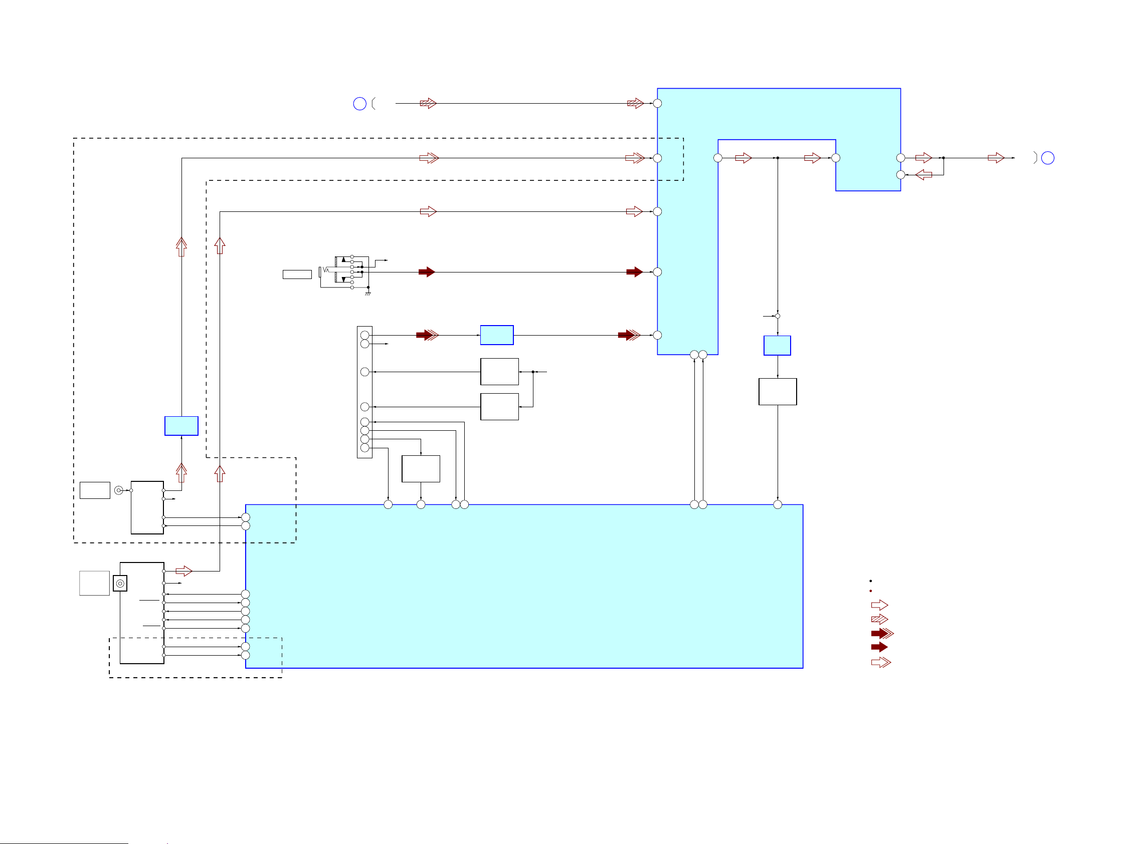
HCD-MX500i/MX550i
HCD-MX500i/MX550i
2020
R-CH
R-CH
CN01
AUDIO IN
J302
28
SDA27SCL
13
IN-L1
VOL L
1 IN-L2
IN-L3
VOL IIC_SDA/E2P-SDA
47
VOL IIC_CLK/E2P-CLK
48
AUDIO_LEVEL_INPUT
12
SEL L
25OUT L
24SB L
ELECTRICAL VOLUME,
INPUT SELECTOR
IC502
: TUNER
: CD PLAY
: iPod/iPhone
SIGNAL PATH
R-ch is omitted due to same as L-ch.
: AUDIO IN
A
B
CD-L
SP_L
7IN-L5
CN332
(iPod/iPhone Dock)
27
28
LINE AMP
IC503
BUFFER
IC515
R-CH
18
19
13
LINE-OUT-L
LINE-OUT-R
RXD
10
Acc ID
TXD
Acc PWR(3.3V)
30
DGND
iPod_RxD_IN
iPod_TxD_OUT
iPod_WAKE
3
75
iPod_DET
76
78 77
: DAB
DAB1
DAB TUNER
MODULE
S1_DIN
S1_DOUT
35 DAB TxD_OUT
36 DAB RxD_IN
AUDR
AUDL
LINE AMP
IC511
SYSTEM CONTROLLER
IC401 (2/4)
ANTENNA
DAB 75:
FM 75:
COAXIAL
ANTENNA
TU1
TUNER (FM)
L-OUT
DO/STEREO
CE
TUNED
DI
CLK
R-OUT R-CH
ST_CE
52
ST_CLK
54
ST_DI/STEREO
55
ST_DO
53
ST_TUNED
51
RDS DATA
RDS INT
RDS_DATA
56
RDS-INT
18
(MX500i: AEP/MX550i)
(MX550i)
iPod POWER
DETECT
Q505
iPod +5V
20
Acc DET
iPod POWER
DETECT
Q506
iPod WAKE
UP DETECT
Q512
AUDIO INPUT
DETECT
Q504, 517
R-CH
32
IN-L45
66
+
5-2. BLOCK DIAGRAM - TUNER, iPod/iPhone, AUDIO IN Section -
(Page 19)
(Page 21)
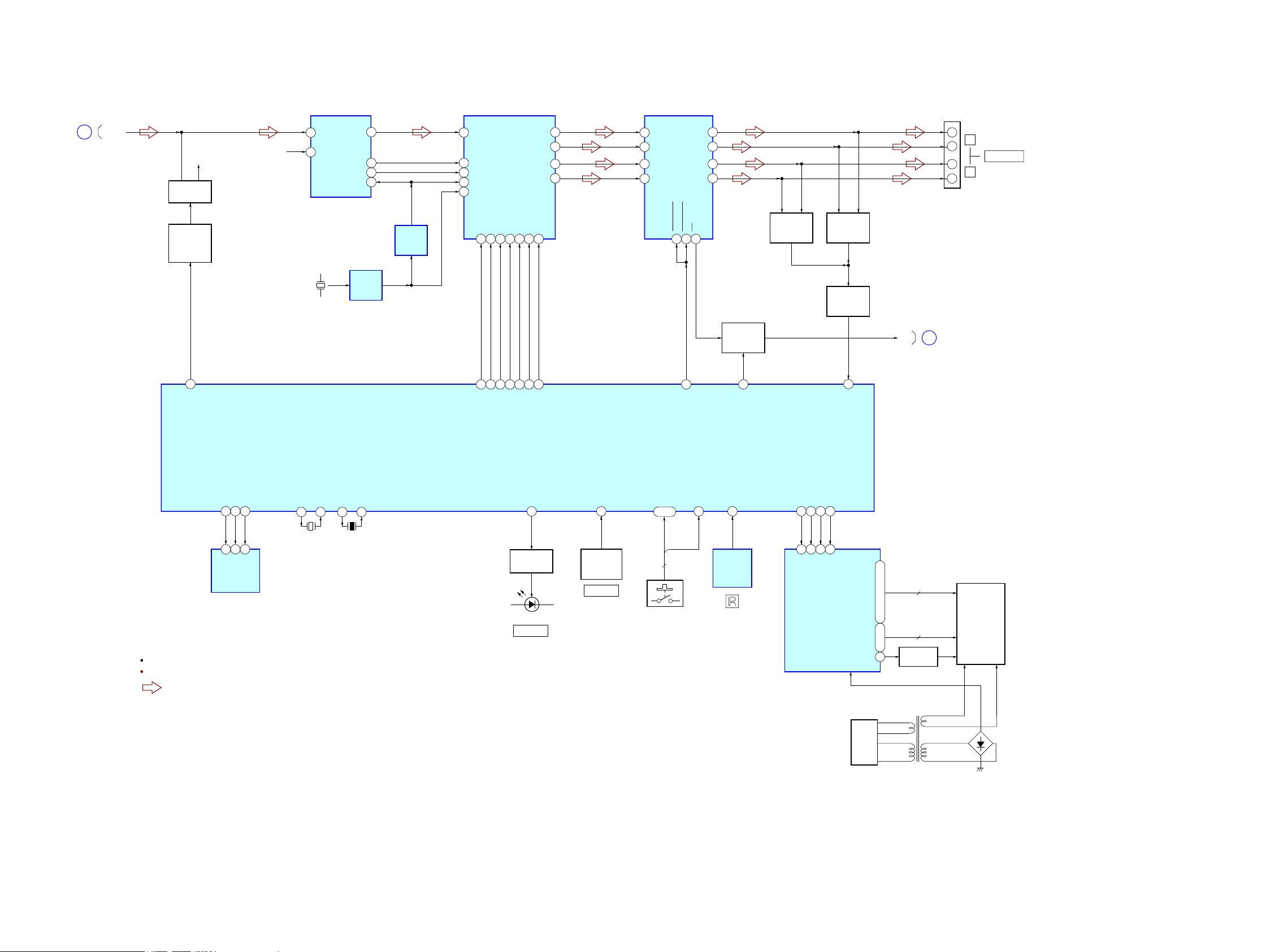
HCD-MX500i/MX550i
HCD-MX500i/MX550i
2121
B
SP-L
SYSTEM CONTROLLER
IC401 (3/4)
: TUNER
SIGNAL PATH
R-ch is omitted due to same as L-ch.
C
SD
SPEAKERS
+
–
–
+
R
L
TB322
17
RESET_CD5SD
PWM_C
PWM_D
7
RESET_AB
S-MASTER_RESET
39
39
OUT_A
36
OUT_B
31
OUT_C
28
OUT_D
6 PWM_A
18
16
PWM_B
8
S-MASTER_DCP
OVER LOAD
DETECT
Q702, 703
PROTECT
DETECT
Q701
LED DRIVE
Q623
BYPASS
73
OVER LOAD
DETECT
Q752, 753
DIGITAL POWER AMP
IC707
11
OUTL1
9
OUTL2
6
OUTR1
4
OUTR2
STREAM PROCESSOR
IC705
A/D CONVERTER
IC711
34
TA_LINE_MUTE
MUTING
Q106
MUTING
CONTROL
SWITCH
Q507, 508
82
PROTECT
DETECT
Q516
X703
49.152MHz
S-MASTER_DATA
40
SCDT
21
S-MASTER_SHIFT
42
S-MASTER_LATCH
43
S-MASTER_PG_MUTE
37
S-MASTER_SOFT_MUTE
38
S-MASTER_NSP_MUTE
44
SCSHIFT22SCLATCH23PGMUTE20SOFTMUTE19NSPMUTE
18
S-MASTER_INIT
45
INIT
27
31 DATA2 AINL
1 AINRR-CH
R-CH
SCLK
12
SDTO
9
LRCK
10
MCLK
11
BCK
30
LRCK
29
XFSIIN
36
XFSOIN
48
CLOCK
BUFFER
IC709
CLOCK
SHIFT
IC703
54
CLKB
53
CSB
55
32
DIN
ND621
FLUORESCENT
INDICATOR
TUBE
G2R - G11
SG1 - SG35,
AD1, AD2
33 - 42 61 - 64, 1 - 31, 60, 59
GR1
1
FL/LCD DO2FL/LCD SCL
24
iPod CP IIC SDA22iPod CP IIC SCL26iPod CP RESET
3
FL/LCD CS
52
RSTB
61
FL/LCD RESET
GRID DRIVE
Q622
FLUORESCENT
INDICATOR
TUBE DRIVER
IC621
SIRCS_IN
REMOTE
CONTROL
RECEIVER
IC622
4
I_KEY WAKE UP_POWER & DISPLAY
74
VOLUME_JOG
72
STBY_LED
46
KEY_1, KEY_2
T621
DC/DC CONVERTER
TRANSFORMER
D621, 622
RECT
VEE
OSC
Q621
X402
5MHz
Xout
Xin
13 15
X401
32.768kHz
EEPROM
IC402
Xcout
Xcin
11 10
S621 - 632
(PANEL KEYS)
70, 71
2
37
10
STANDBY
VOLUME
KEY_1
D624
12
I2C_SCL
4
RESET
13
I2C_SDA
ROTARY
ENCODER
RV621
5-3. BLOCK DIAGRAM - OUTPUT, PANEL Section -
(Page 20)
(Page 22)
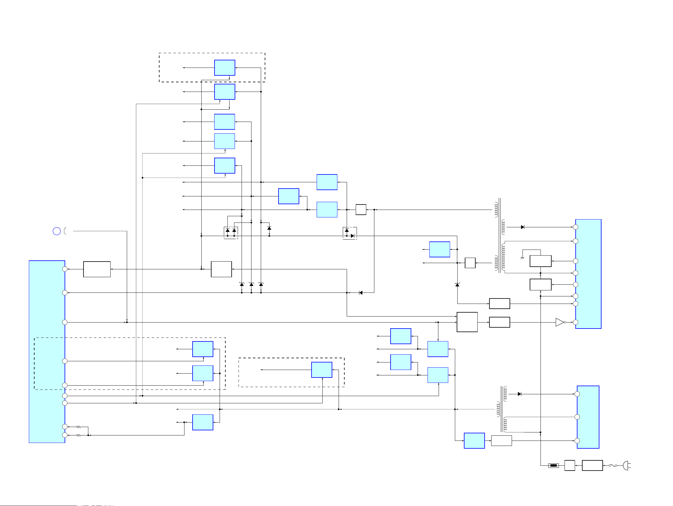
HCD-MX500i/MX550i
HCD-MX500i/MX550i
2222
20
12
POWER ON 63
D923
POWER CONTROL
IC11
D14
D603
EVER +4V
EVER +3.3V
(AC IN)
F1
LINE FILTER
T1
RECT
D1
TH1
D902
15 VS
18 VD
1 VSENSE
2 F/B
16 VG-H
12 VG-L
8VC1
POWER CONTROL
IC601
5 DRAIN
2FB
4VCC
ISOLATOR
PC11
ISOLATOR
PC602
ISOLATOR
PH601
T031
MAIN POWER
TRANSFORMER
T603
SUB POWER
TRANSFORMER
POWER
ON/OFF
CONTROL
Q901 - 903
SWITCHING
Q012
SWITCHING
Q011
SHUNT
REGULATOR
IC909
RECT
D904
+12V
REGULATOR
IC710
Q601
9OCP
D905
AMP +27V
AMP +12V
RESET
69
AC_DET
D927 D914
83
POWER_PROTECT
+3.3V
REGULATOR
IC405
AMP +3.3V
+3.3V
REGULATOR
IC704
VBUS +5V
+5V
REGULATOR
IC506
iPod +5V
AMP +1.8V
+1.8V
REGULATOR
IC712
CD D +3.3V
CD D +1.5V
+1.5V
REGULATOR
IC102
DAB +3.3V
+3.3V
REGULATOR
IC671
A +9V
M +7V
+9V
REGULATOR
IC905
A +5V
+5V
REGULATOR
IC908
+7V
REGULATOR
IC904
RECT
D903
D911
D922
AC-CUT
49
DAB-POWER_3.3
USB +3.3V
+3.3V
REGULATOR
IC509
85
BOLERO/iPod_ON
86
ZIPANG_ON
DAB +1.2V
+1.2V
REGULATOR
IC672
50
DAB-POWER_1.2
C
SD
PROTECT
DETECT
Q904
OVER CURRENT
PROTECT
Q509
SYSTEM CONTROLLER
IC401 (4/4)
D913
(MX550i)
(Except Canadian)
(Except Canadian)
+3.3V
REGULATOR
IC508
+5V
REGULATOR
IC510
CD A +3.3V
+3.3V
REGULATOR
IC505
CD +5V
+5V
REGULATOR
IC504
A/D +3.3V
+3.3V
REGULATOR
IC702
5-4. BLOCK DIAGRAM - POWER SUPPLY Section -
(Page 21)
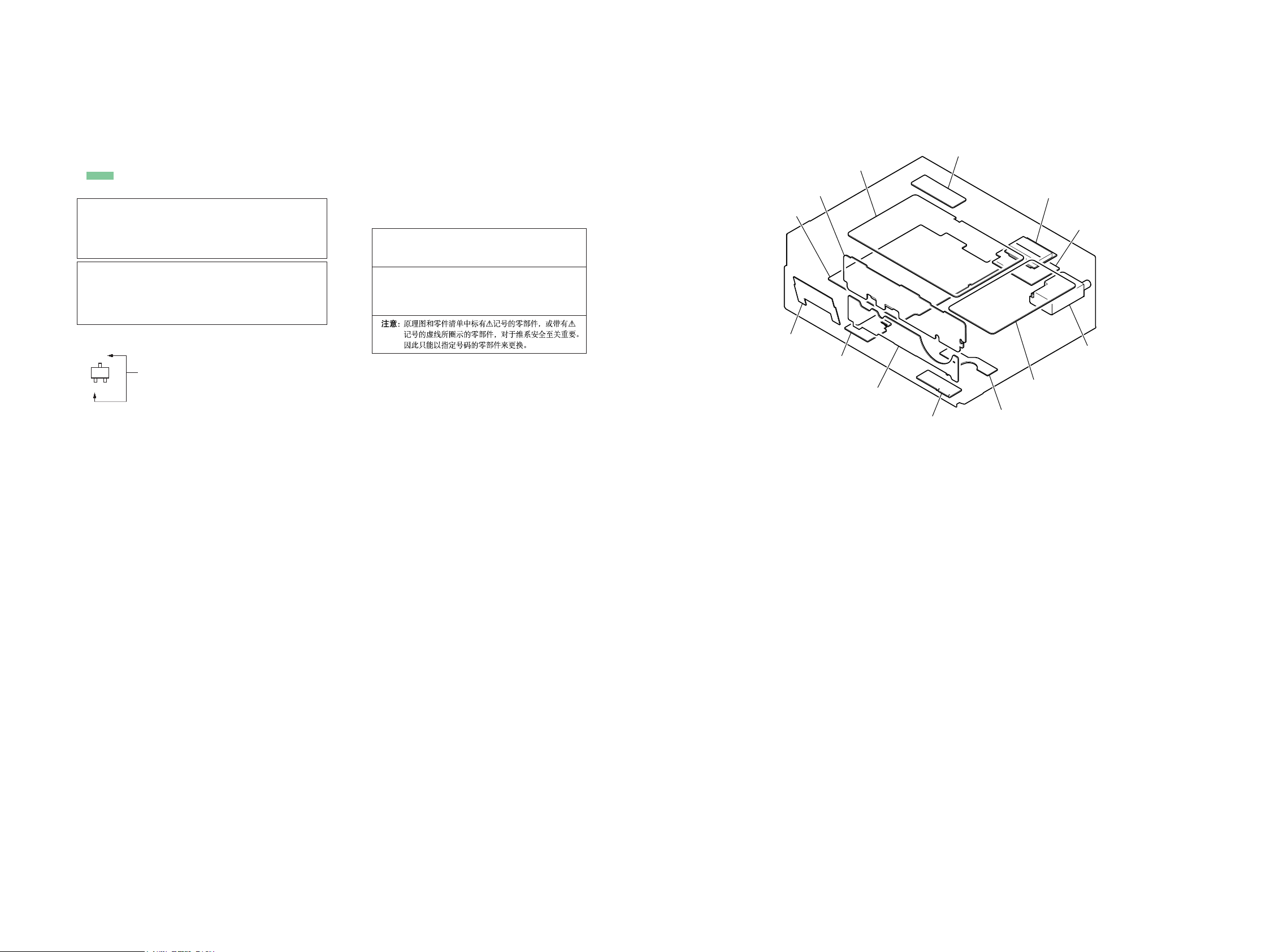
HCD-MX500i/MX550i
HCD-MX500i/MX550i
2323
For Schematic Diagrams.
Note:
• All capacitors are in μF unless otherwise noted. (p: pF) 50
WV or less are not indicated except for electrolytics and
tantalums.
• All resistors are in Ω and 1/4 W or less unless otherwise
specifi ed.
• f : Internal component.
• 2 : Nonfl ammable resistor.
• C : Panel designation.
THIS NOTE IS COMMON FOR PRINTED WIRING BOARDS AND SCHEMATIC DIAGRAMS.
(In addition to this, the necessary note is printed in each block.)
• A : B+ Line.
• B : B– Line.
• Voltages and waveforms are dc with respect to ground
under no-signal (detuned) conditions.
– BD96/BD96U Board –
no mark : CD PLAY
– Other Boards –
no mark : TUNER FM
< > : TUNER DAB
* : Impossible to measure
• Voltages are taken with VOM (Input impedance 10 MΩ).
Voltage variations may be noted due to normal production
tolerances.
• Waveforms are taken with a oscilloscope.
Voltage variations may be noted due to normal production
tolerances.
• Circled numbers refer to waveforms.
• Signal path.
F : TUNER
J : CD PLAY
d : USB
i : iPod/iPhone
f : AUDIO IN
• Abbreviation
CH : Chinese model
CND : Canadian model
SP : Singapore model
For Printed Wiring Boards.
Note:
• X : Parts extracted from the component side.
• Y : Parts extracted from the conductor side.
• f : Internal component.
• : Pattern from the side which enables seeing.
(The other layers’ patterns are not indicated.)
• Indication of transistor.
Caution:
Pattern face side:
(SIDE B)
Parts face side:
(SIDE A)
Parts on the pattern face side seen
from the pattern face are indicated.
Parts on the parts face side seen from
the parts face are indicated.
Note: The components identifi ed by mark 0 or
dotted line with mark 0 are critical for safety.
Replace only with part number specifi ed.
Note: Les composants identifi és par une marque
0 sont critiques pour la sécurité.
Ne les remplacer que par une piéce portant
le numéro spécifi é.
Caution:
Pattern face side:
(Conductor Side)
Parts face side:
(Component Side)
Parts on the pattern face side seen
from the pattern face are indicated.
Parts on the parts face side seen from
the parts face are indicated.
• Circuit Boards Location.
• Abbreviation
CH : Chinese model
CND : Canadian model
SP : Singapore model
C
Q
B
E
These are omitted.
FL board
POWER board
IP board
MAIN board
JACK board
KEY board
SP board
USB board
(Except Canadian)
MODULE (DAB TUNER) (MX550i)
DAB board (MX550i)
TUNER (FM)
BD96 board (Canadian)
BD96U board (Except Canadian)
MS-203 board
 Loading...