

Page 1

HCD-MJ1
SERVICE MANUAL
Ver 1.2 2003.12
r HCD-MJ1 is the tuner, CD
amplifier and MDsection in
MJ-L1.
CD
US and foreign patents licensed from Dolby
Laboratories Licensing Corporation.
CD ptayer section
System Compact disc and digital audio system
Laser Semiconductor laser (λ=780 nm)
Emission duration: continuous
Laser output
Max 44.6 µW*
* This output is the value measured at a
distance of 200mm from the objective
lens surface on the Optical Pick-up
Block with 7 mm aperture.
Wavelength
780 - 790 nm
Frequency response
2 Hz - 20 kHz
MiniDisc deck section
System MiniDisc digital audio system
Disc MiniDisc
Laser Semiconductor laser (λ= 780 nm)
Laser output
Max 44.6 µW*
* This output is the value measured at a
distance of 200mm from the objective
lens surface on the Optical Pick-up
Block with 7 mm aperture.
SPECIFICATIONS
Laser diode properties
Materi.II: GaAIAs
Revolutions (CLV)
Approx. 400 rpm to 900 rpm
Error correction
Adv,Inced Cross IntL•rleave Rced
Solomon Code (ACIRC)
Sampling frequency
44.1 kHZ
Modulation system
EFM
(Eight-to-Fourteen Modula tion)
Number of channels
2 stereo channels
Frequency response
5 Hz - 20 kHz
Wow and fluttei
Below measurable limit
Tuner section
FM tuner section
Tuning range
US, Canadian model
: 87.5 - 108.0 MHz (100 kHz step)
Except US, Canadian model
: 87.5 - 108.0 MHz (50 kHz step)
Section
MD Model Name Using Similaar Mechanism NEW
Section Mini Disc Mechanism Type MDM-2ER
US Model
Canadian Model
AEP Model
UK Model
E Model
Model Name Using Similar Machanism HCD-D1/T1
––––––––––––––––––––––––––––––––––––––––––––––––––––––––––––––––––––––––––––––––––––––––––––––––––––––––
CD Mechanism Type CDM13C-5BD19
––––––––––––––––––––––––––––––––––––––––––––––––––––––––––––––––––––––––––––––––––––––––––––––––––––––––
Base Unit Name BU-5BD19
––––––––––––––––––––––––––––––––––––––––––––––––––––––––––––––––––––––––––––––––––––––––––––––––––––––––
Aerial FM Iead aerial
Aerial terminal
Intermediate frequency
AM tuner section
Tuning range
US, Canadian model
AEP, UK, German, Italian, Singapore,
Hong kong model
Aerial AM Ioop aerial,
Intermediate frequency
Timer section
System Quartz lock system
Timer setting
Sleep timer
75 ohm unbalanced
l0.7 MHz
: 530 - 1.710 kHz
(with the interval set at 10 kHz)
: 531 - 1.602 kHz
(with the interval set at 9 kHz)
External aerial terminals
450 kHz
One-minute step
10-minute step. max. 90 minutes
– Continued on pag 2 –
9-960-606-13
2003L02-1
© 2003.12
FLAT COMPONENT SYSTEM
Sony Corporation
Home Audio Company
Published by Sony Engineering Corporation
Page 2

Amplifier section
DIN power output
Continuous RMS power output
US, Canadian model :
Except US, Canadian model :
Music power output
Inputs TAPE (phono jacks):
Outputs TAPE (phono jacks):
Supplied accessories
General
Power requirements
Destination Power Power
US, Canadian model 120V AC,60Hz 95W
AEP, UK, German
Italian model
E, Singapore,
Hong Kong model
Dimensions
Mass Approx. 7.0 kg (15 Ib 7 oz)
Design and specifications are subject to
change without notice.
30 W + 30 W
(6 ohms at 1 kHz, DIN)
30 W + 30 W
(6 ohms at 40Hz-16kHz, 1.0% THD)
35 W + 35 W
(6 ohms at 1kHz, 5% THD)
POPO 350W
40 W + 40 W
(6 ohms at 1 kHz, lO% THD)
70W+70W
(6 ohms at 1 kHz. lO% THD)
voltage 250 mV
impedance 47 kilohms
voltage 250 mV
impedance 1 kilohms
PHONES (stereo phone jack):
accepts headphones of 8 ohms
or more.
Sony RM-SMJI Remote (1)
Sony lithium battery. CR2025 (1 )
FM lead aerial (1)
AM loop aerial (1)
Speaker cords (2)
requirements consumption
220-230V AC, 50/60Hz
110-120V/ 220-240V AC,
50/60Hz Adjustable with 95W
the Voltage Selector
Approx. 430 x 95 x 290 mm
(17 x 33/4 x 11 1/2 inches) (w/h/d)
incl. projecting parts and controls
95W
TABLE OF CONTENTS
Specifications ............................................................................... 1
1.
SERVICING NOTES ..................................................4
2. GENERAL
Index to parts and Controls .................................................... 5
3.
DISASSEMBLY
3-1. Case (Top) Section and
Plate (T back) Ornamentel Removal............................... 8
3-2. Main board,Tuner board and Display board Removal .... 8
3-3. CD Mechanism, MD Mechanism and
Digital board Removal .................................................... 9
4.
DISC TABLE GETTING OUT PROCEDURE
ON THE POWER SUPPLY IS OFF ....................... 10
5.
TEST MODE ............................................................. 11
6. ELECTRICAL ADJUSTMENTS ..................................... 14
7.
EXPLANATION OF IC TERMINALS ...................... 22
8. DIAGRAMS
8-1. Block Diagram –Main Section– ................................. 30
8-2. Block Diagram –MD Section– ................................... 33
8-3. Circuit Boards Location.............................................. 37
8-4. Printed Wiring Boards –Main Section–...................... 38
8-5. Schematic Diagram –Main Section– .......................... 41
8-6. Schematic Diagram –Digital Section– ....................... 46
8-7. Printed Wiring Boards –Digital Section– ................... 51
8-8. Printed Wiring Boards –BD : MD Section– ............... 54
8-9. Schematic Diagram –BD : MD Section– ................... 57
8-10. Schematic Diagram –Display Section– ...................... 61
8-11. Printed Wiring Boards –Display Section–.................. 65
8-12. Schematic Diagram –BD : CD Section– .................... 70
8-13. Printed Wiring Boards –BD : CD Section– ................ 73
8-14. IC Block Diagram....................................................... 75
9. EXPLODED VIEWS
9-1. Cabinet Section............................................................. 79
9-2. Chassis Section-1.......................................................... 80
9-3. Chassis Section-2.......................................................... 81
9-4. MD Mechanism Section (MDM-2ER) ......................... 82
9-5. Base Unit Section (MD) (MBU-2) ............................... 83
9-6. CD Mechanism Section-1 (CMD-5BD19) ................... 84
9-7. CD Mechanism Section-1 (CMD-5BD19) ................... 85
10. ELECTRICAL PARTS LIST ............................................ 86
– 2 –
Page 3

MODEL IDENTIFICATION
MODEL NO. HCD-MJ1
FLAT COMPONENT SYSTEM
US, Canadian model : AC120V ⁄60Hz
AEP, UK, German, Italian model
: AC220-230V ⁄50/60Hz
Hong kong, Sinagpore mdel
: AC110-120V/AC220-240V ⁄50/60Hz
Laser component in this product is capable of emitting radiation
exceeding the limit for Class 1.
For customers in Europe
This Compact Disc player is
classified as a CLASS 1 LASER
product.
The CLASSLASER
PRODUCT label is located on
the rear exterior.
SAFETY CHECK-OUT
After correcting the original service problem, perform the following safety check before releasing the set to the customer :
Check the antenna terminals, metal trim, “metallized” knobs,
screws, and all other exposed metal parts for AC leakage. Check
leakage as described below.
LEAKAGE TEST
The AC leakage from any exposed metal part to earth ground and
from all exposed metal parts to any exposed metal part having a
return to chassis, must not exceed 0.5mA (500 microampers).
Leakage current can be measured by any one of three methods.
1. A commercial leakage tester, such as the Simpson 229 or RCA
WT-540A. Follow the manufacturers’ instructions to use these
instruments.
2. A battery-operated AC milliammeter. The Data Precision 245
digital multimeter is suitable for this job.
3. Measuring the voltage drop across a resistor by means of a
VOM
or battery-operated AC voltmeter. The “limit” indication is
0.75V, so analog meters must have an accurate low-voltage
scale. The Simpson 250 and Sanwa SH-63Trd are examples of a
passive VOM that is suitable. Nearly all battery operated digital
multimeters that have a 2V AC range are suitable. (See Fig. A)
To Exposed Metal
Parts on Set
AC
0.15
1.5k
µ
F
Ω
Voltmeter
(0.75V)
This caution label is located
insuide the unit.
CAUTION
Use of controls or adjustments or performance of procedures other
than those specified herein may result in hazardous radiation exposure.
Earth Ground
Fig. A. Using an AC voltmeter to check AC leakage.
SAFETY-RELATED COMPONENT WARNING!!
COMPONENTS IDENTIFIED BY MARK ! OR DOTTED LINE
WITH MARK !ON THE SCHEMATIC DIAGRAMS AND IN THE
PARTS LIST ARE CRITICAL TO SAFE OPERATION.
REPLACE THESE COMPONENTS WITH SONY PARTS WHOSE
PART NUMBERS APPEAR AS SHOWN IN THIS MANUAL OR IN
SUPPLEMENTS PUBLISHED BY SONY.
ATTENTION AU COMPOSANT AYANT RAPPORT
À LA SÉCURITÉ!
LES COMPOSANTS IDENTIFIÉS PAR UNE MARQUE ! SUR LES
DIAGRAMMES SCHÉMATIQUES ET LA LISTE DES PIÈCES SONT
CRITIQUES POUR LA SÉCURITÉ DE FONCTIONNEMENT. NE
REMPLACER CES COMPOSANTS QUE PAR DES PIÈCES SONY
DONT LES NUMÉROS SONT DONNÉS DANS CE MANUEL OU
DANS LES SUPPLÉMENTS PUBLIÉS PAR SONY.
– 3 –
Page 4

SECTION 1
SERVICING NOTES
NOTES ON HANDLING THE OPTICAL PICK-UP
BLOCK OR BASE UNIT
The laser diode in the optical pick-up block may suffer electrostatic
breakdown because of the potential difference generated by the
charged electrostatic load, etc. on clothing and the human body.
During repair, pay attention to electrostatic breakdown and also use
the procedure in the printed matter which is included in the repair
parts.
The flexible board is easily damaged and should be handled with
care.
NOTES ON LASER DIODE EMISSION CHECK
The laser beam on this model is concentrated so as to be focused on
the disc reflective surface by the objective lens in the optical pick-up
block. Therefore, when checking the laser diode emission, observe
more than 30 cm away from the objective lens.
ENTERING TEST MODE
When you press the DISP button, p button, and EDIT button at the
same tilne, the system goes into key , fluorescent tube, jogr and LED
check mode.
r Fluorescent tube check
All the lights light up. Then, each time you press the ENTER but-
ton, the display mode changes as shown below.
nAll lit n partially lit l n partially lit 2
r LED check
When you turn the jog dial, the LEDS change froln all lit to indi-
vidually lit.
r Key check
The EDIT/NO button puts the system into key/jog check mode .
When you press a button, the number is counted up.
However, pressing a button again that you already pressed does
not count up the number.
Turning the jog dial to the right increases the jog count display,
turning the jog dial to the left decreases the jog count.
When you have pressed all the buttons and “KEY= 0K” is dis-
played, pressing any button ends test Inode.
Cautions when replacing IC121 and
IC171 on the BD board
A change has been made from CXD2535BR due to a modification of
IC121 on the BD board in this unit.
Accompanying this modification, a portion of the nonü]volatile
memory of IC171 (XC24CO1S) has been changed.
Conversely, when IC121 has been replaced, use CXD2535BR and
rewrite the contents of IC171.
Contents of non-volatile memories CXD2535BR
Address CXD2535BR
15 93
2D 1A
2E 1A
Rewrite Procedure for Non-volatile Memory
(1) With the power switched off and the power plug plugged into a
socket. press the BASS/TREBLE button. CLOCK button, and MD
button more than one at a time in order.
(2)Rotate the JOG dial knob and display the “EEP MODE”.
When you press the YES key, the display changes to show
“EEP**@@”.
(Here, **indicates the address, and @@ indicates the data.)
(3)Rotate the JOG dial knob and display the “EEP 15 @@”.
(4)When you press the CD SYNCHRO button, “EEP 15 @@>@@”
is displayed so then turn the JOG dial knob to show ügEEP 15
@@>93”
(5)Press the YES key and “COMPLETE” will appear for a moment
and data shown as “EEP 15 93” is being rewritten.
(6)Rewrite address 2D and address 2E, into 1A using steps (3) to (5)
above.
(7) When all changes are complete, press the NO key and display
“EEP MODE”.
(8)Press the REPEAT button. If no disc is loaded, the time is dis-
played, so unplug the power plug. If a disc is loaded, the disc is
ejected, then the time is displayed. Unplug the power plug from
the socket to end EEP rewrite mode. (See “How to end test mode”
below .)
Note: Changes in the contents of non-volatile memory are not re-
flected until the power is switched off, then on.
HOW TO END TEST MODE
Method :
l Press the REPEAT button.
2 If no disc is loaded, the time is displayed. If a disc is loaded, the
disc is ejected, then the time is displayed .
3 Unplug the power plug from the socket.
– 4 –
Page 5

SECTION 2
GENERAL
This section is extracted from instruction manual.
– 5 –
Page 6

– 6 –
Page 7

– 7 –
Page 8
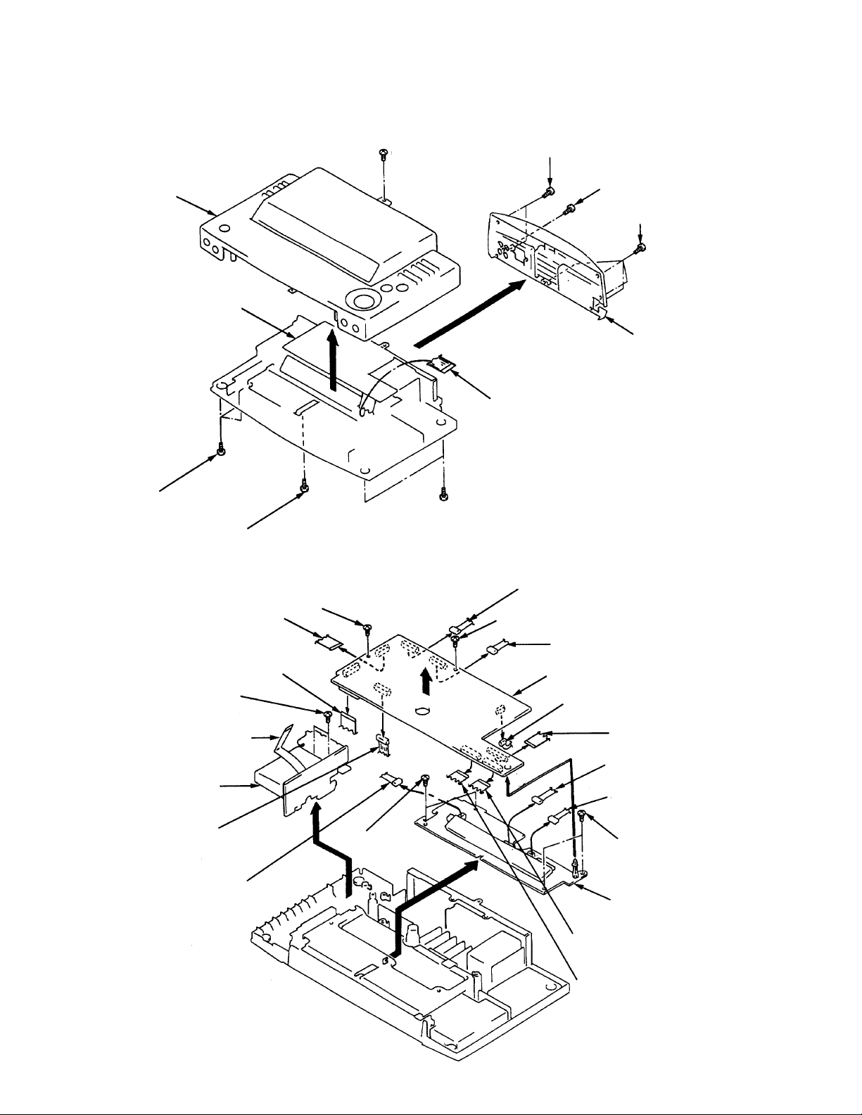
SECTION 3
DISASSEMBLY
Note : Follow the disassembly procedure in the numerical order given.
3-1. CASE (TOP) SECTION AND PLATE (T BACK) ORNAMENTEL REMOVAL
4
+BVTT 3 x 6
CASE (TOP) SECTION
3
MAIN BOARD
1
+BVTT 3 x 10
2
+BVTP 3 x 10
1
+BVTT 3 x 10
7
5
+BVTP 3 x 10
6
+BVTT 3 x 10
5
+BVTP 3 x 10
3-2. MAIN BOARD,TUNER BOARD AND DISPLAY BOARD REMOVAL
1
4
Wire (flat type) (13CORE) (CN103)
to TERMINAL BOARD (CN602)
3
Wire (flat type) (19CORE) (CN105)
to CDM
!§
+BVTP 3 x 8
!¶
Wire (flat type) (15CORE) (CN4)
to MAIN BOARD (CN104)
TUNER BOARD
8
CN106 (8pin)
to DIGITAL BOARD (CN281)
+BVTP 3 x 8
!•
!¢
+BVTP 3 x 8
PLATE (T BACK) ORNAMENTAL
8
Wire (flat type) (11CORE)
to Switch (R) BOARD
5
CN102 (8pin)
to AMP BOARD (CN901)
1
+BVTP 3 x 8
6
CN101 (9pin)
to TRANSFORMER BOARD (CN804)
MAIN BOARD
7
CN111 (3pin) toFAN801
2
4
Wire (flat type) (21CORE) (CN109)
to DIGITAL BOARD (CN223)
!™
CN702 (5pin) to CDM
!£
CN706 (3pin)
to SENSOR BOARD (CN706)
!¢
+BVTP 3 x 8
!¡
CN701(4pin)
SWTCH (LID) BOARD (CN703)
and MOTOR (LID) BOARD (CN704)
– 8 –
!∞
DISPLAY BOARD
!º
Wire (flat type) (19CORE) (CN110)
to SWITCH (R) BOARD (CN501)
9
Wire (flat type) (19CORE) (CN107)
to DISPLAY BOARD (CN551)
Page 9
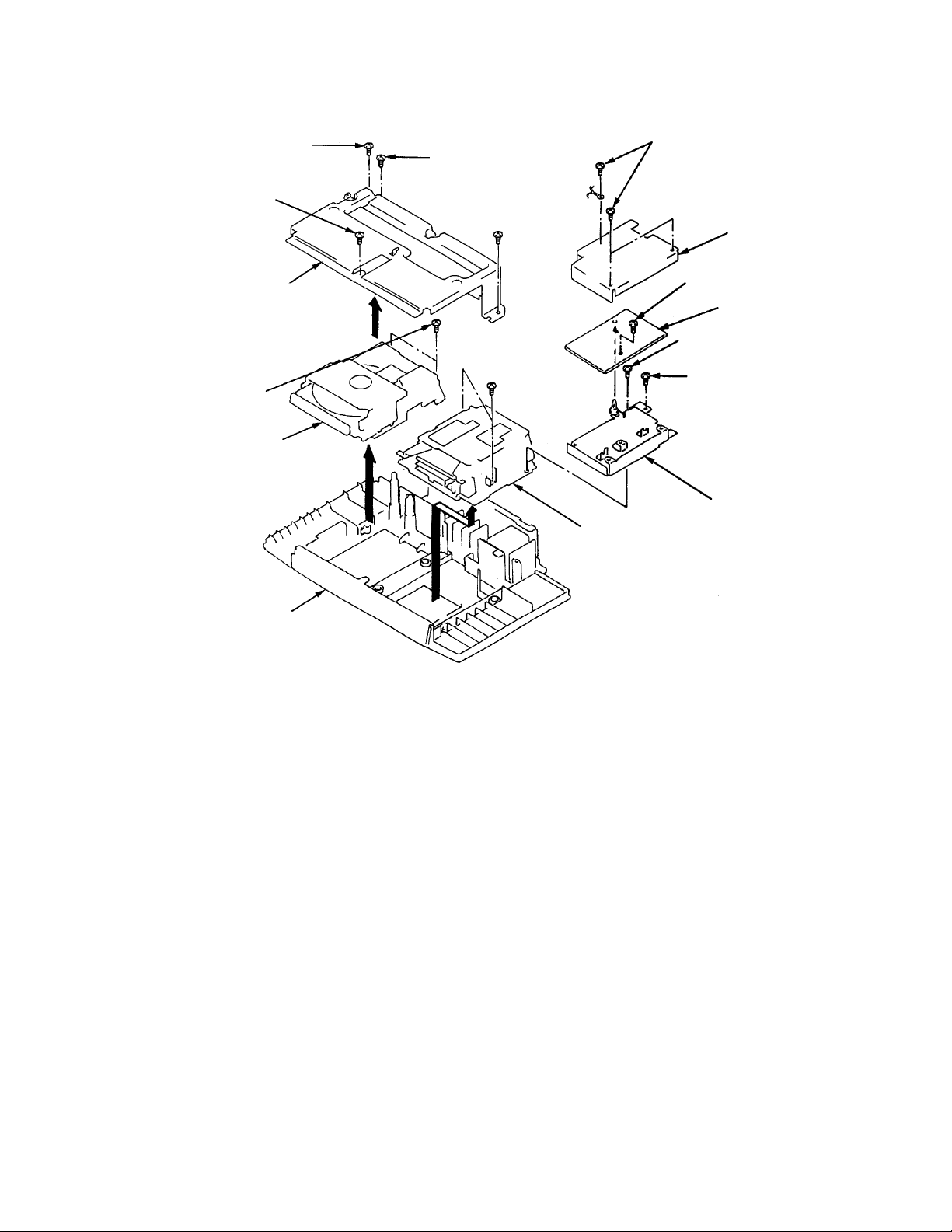
3-3. CD MECHANISM, MD MECHANISM AND DIGITAL BOARD REMOVAL
1
+BVTP 3 x 8
3
+BVTT 3 x 6
CHASSIS (M)
!£
+BVTT3 x 10
CD MECHANISM SECTION
4
!¢
2
+BVTT3 x 10
!¡
1
+BVTP 3 x 8
+BVTT3 x 10
MD MECHANISM SECTION
5
+BVTT3 x 6
7
9
+BVTT 3 x 10
!º
SHELDE (T)
+BVTP 3 x 8
DIGITAL BOARD
+BVTP 3 x 8
SHELDE
CASE (BOTTOM) SECTION
!™
– 9 –
Page 10

SECTION 4
DISC TABLE GETTING OUT PROCEDURE ON THE POWER SUPPLY IS OFF
1
TWEEZERS
DOOR
2
CAM
4
3
DISC TABLE
– 10 –
Page 11
SECTION 5
TEST MODE
5-1. How to enter the Test Mode
With the power switched of f and the po wer plug plugged into a socket, pr ess the B ASS/TREBLE b utton, CLOCK b utton, and MD b utton more
than one at a time in order.
5-2. How to Release the Test Mode
Press the REPEAT button.
5-3. Basic Operations of the Test Mode
All operations are performed using the JOG dial (Rotary Encoder) , YES (ENTR/TES)button, and NO (EDIT/ON)button.
The functions of these keys are as follows.
Function Contents
JOG dial Changes parameters and modes.
YES button Proceeds onto the next setp. inalizes input
NO button Returns to previous step. Stops operations.
5-4. Selecting the Test Mode
Eight test modes are selected by turning the AMS knob.
Display Contents
TEMP ADJUST Temperature compnsation offset adjustment
LDPWR ADJUST Laser power adjustment
EFBAL ADJUST Trav erse adjustment
FBIAS ADJUST Focus bias adjustment
FBIAS CHECK Focus bias check
CPLAY MODE Continuous playback mode
CREC MODE Continuous recording mode
EEP MODE Non-volatile memory mode*
For detailed description of each adjustment mode, refer to 6. Electrical Adjustments.
If a different adjustment mode has been selected by mistake, press the NO button to exit from it.
* The EEP MODE is not used in servicing. If set accidentally, press the NO button immediately to exit it.
5-5-1. Operating the Continuous Playback Mode
1. Entering the continuous playback mode
1 Set the disc in the unit (either MO or CD).
2 Rotate the JOG dial and display “CPLAY MODE”.
3 Press the YES button to change the display “CPLAY IN”.
4 When access completes, the display changes to “C1 = AD = ”
Note : The “ ” displayed are arbitrary numbers.
2. Changing the parts to be played back
1 Press the YES button during continuous playback to change the display to “CPLAY MID”, “CPLAY OUT”.
When pressed another time, the parts to be playedback can be changed.
2 When access completes, the display changes to “C1 = AD = ”
Note : The “ ” displayed are arbitrary numbers.
3. Ending the continuous playback mode
1 Press the No button. The display will change to “CPLAY MODE”.
2 Press the MD § button and remove the disc.
Note 1 : The playback start addresses for IN, MID, and OUT are as follows.
Press the DISPIAY button twice to display thae address. Pressing the DISPIAY buttan again returns the display to
“C1 = AD = ”
IN 40h cluster
MID 300h cluster
OUT 700h cluster
– 11 –
Page 12

5-5-2. Operating the Continuous Recording Mode
1. Entering the continuous recording mode
1 Set the MO disc in the unit.
2 Rotate the JOG dial knob and display “CREC MODE”.
3 Press the YES button to change the display to “CREC IN”.
4 When access completes, the display changes to “CREC ( ) and REC lights up.
Note : The “ ” displayed are arbitrary numbers.
2. Changing the parts to be recorded
1 When the YES button is pressed during continuous recording. the display changes to “CREC MID”, “CREC OUT”and REC goes off.
When pressed another time, the parts to be recorded can be changed.
2 When access completes, the display changes to “CREC ( ) and REC lights up.
Note : The “ ” displayed are arbitrary numbers.
3. Ending the continuous recording mode
1 Press the No bottan. The display change to CREC MODE” and REC goes off.
2 Press the MD § button and remove the disc.
Note 1 : The recording start addresses for IN, MID, and OUT are as follows.
IN 40h cluster
MID 300h cluster
OUT 700h cluster
Note 2 : The No buttton can be used to stop recording anytime.
Note 3 : During the test mode, the erasing-protection tab will not be detected. Therefore be careful not to set the continuous recording mode
when a disc not be erased is set in the unit.
Note 4 : Do not perform continuous recording for long periods of time above 5minutes.
Note 5 : During continuous recording, be careful not to apply vibration.
5-5-3. Non-Volatile Memory Mode (EEP MODE)
This mode reads and writes the contents of the nonü]volatile memory.
It is not used in servicing. If set accidentally, press the No button immediately to exit it.
5-6. Functions of Other buttons
Function Contents
^
p Stops continuouse playback and continuouse recording.
) The sled moves to the outer circumference only when this is pressed.
0 The sled moves to the inner circumference only when this is pressed.
r Turns recording ON/OFF when presed during continuoos playback.
SCROOLL Switches butween the pit and groove modes when pressed.
DISPLAY Switches the display whin pressed. Returns to previous step. Stops operations.
Sets continuous playback when pressed in the STOP state.
When pressed during continuouse playback,the tracking servo turns ON/OFF.
Note : The erasing-protection tab is not detected during the test mode. Recording will start regardless of the position of the erasing-protection
tab when the r (REC) button is pressed.
– 12 –
Page 13

5-7. Test Mode Displays
Each time the DISPLAY button is pressed, the display changes in the following order.
MODE displaynError rate displaynAddress display
1. MODE display
Displays “TEMP ADJUST” , “CPLAY MODE” , etc.
2. Address display
Addresses are displayed as follows.
h = s = (MO pit and CD)
h = a = (MO groove)
h = Header address
s = SUBQ address
a = ADIP address
* A ‘ ’ display appears when the address cannot be loaded.
3. Error rate display
Error rates are displayed as follows.
C1 = AD =
C1 = Indicates C1 error
AD = Indicates ADER
5-8. Meanings of Other Displays
Display Contents
Light Off Blinkig
( During continuous playbak STOP
^ Tracking servo OFF Tracking servo ON
REC Recording mode ON Recording mode OFF
SYNC CLV LOCK CLV UNLOCK
TRACK Pit Groove
DISC High refiection Low refiection
LEVEL-SYNC CLV-S CLV-A
MEMORY ABCD adjustment completed
SHUFFLE Focus auto gain successful Focus auto gain successful
Tracking auto gain successful Tracking auto gain failed
5-9. Precautions for Use of Test Mode
2 As loading related operations will be performed regardless of the test mode operations being performed, be sure to check that the disc
is stopped before setting and removing it.
Even if the MD § button is pressed while the disc is rotating during continuous playback, continuous recording, etc., the disc will not
stop rotating.
Therefore, it will be ejected while rotating.
* Always press the NO button before pressing the MD § button.
2 The erasing-protection tab is not detected in the test mode. Therefore, when modes which output the recording laser power such as
continuous recording mode and traverse adjustment mode, etc. are set, the recorded contents will be erased regardless of the position
of the tab. When using a disc that is not to be er ased in the test mode, be careful not enter the continuous recording mode and tra verse
adjustment mode.
– 13 –
Page 14

SECTION 6
ELECTRICAL ADJUSTMENTS
PRECAUTION
6-1. Precautions for Checking Laser Diode Emission
To check the emission of the leaser diode during adjustments, never
view directly from the top as this may lose your eye-sight.
6-2. Precautions for Use of optical pickup (KMS-210A)
As the laser diode in the optical pickup is easily damaged by static
electricity, solder the laser tap of the flexible board when using it.
Before disconnecting the connector, desolder first. Before connecting the connector,be careful not to remove the solder. Also tale adequate measures to prevent damage by static electricity. Handle the
flexible board with care as it breaks easily.
Laser tap
Optical pickup flexible board
6-3. Precautions for Adjustments
1) when replacing the following parts, perform the adjustments and
checks with O in the order shown in the following table.
Optical BD (MD) BOARD
pickup IC171 D101 IC101,IC121,IC191
1. Temperature
compensation X O O O
offset adjustment
2. Laser power
adjustment
3. Traverse
adjustment
4. Focus bias
adjustment
5. Error rate check O O X O
OXX O
OOX O
OOX O
2) Set the test mode when performing adjustments.
After completing the adjustments,exit the test mode.
3) Perform the adjustments in the order shown.
4) Use the following tools and measuring devices.
r Test disc (CD) TDYS-1 (Parts No. 4-963-646-01)
r Laser power meter LPM-8001 (Parts No. J-2501-046-A)
r Oscilloscope
r Digital voltmeter
r Thermometer
5) When observing several signals on the oscilloscope, etc., make
sure that VC and GND do not connect inside the oscilloscope.
(VC and GND will become short-circuited)
6) Do not move RV105 of the BD (MD) board. When replacing it,
adjust to the mechanical center of the semi-fixed resistor.
6-4. Creating MO Continuously Recorded Disc
* This disc is used in focus bias adjustment and error rate check.
The following describes how to create a MO continuous recording disc.
1. Insert a MO disc (blank disc) commercially available.
2. Rotate the JOG dial and display “ CREC MODE”.
3. Press the YES button and display “ CREC IN”.
4. Press the YES button again to display “ CREC MID”.
“ CREC (0300)” is displayed for a moment and recording starts.
5. Complete recording within 5 minutes.
6. Press the NO button and stop recording
7. Press the MD § button and remove the MO disc.
The above has been how to create a continuous recording data for the
focus bias adjustment and error rate check.
Note :
r Be careful not to apply vibration during continuous recording.
– 14 –
Page 15

r
r
6-5. Temperature Compensation Offset Adjustment
Save the temperature data at that time in the non-volatile memory as
25°C reference data.
Note :
1. Usually, do not perform this adjustment.
2. Perform this adjustment in an ambient temperature of 22°C to
28°C. Perform it immediately after the power is turned on when
the internal temperature of the unit is the same as the ambient
temperature
3. When D101 has been replaced, perform this adjustment after the
temperature of this part has become the ambient temperature.
Adjusting Method :
1. Rotate the JOG dial and display “TEMP ADJUST”.
2. Press the YES button and select the “TEMP ADJUST” mode.
3. “TEMP =
”and the current temperature data will be displayed
4. To save the data, press the YES button.
When not saving the data, press the NO button.
5. When the YES button is pressed, “TEMP = SAVE”will be
displayed for some time, followed by “TEMP ADJUST”.
When the NO button is pressed, “TEMP ADJUST” will be displayed.
Specifications :
The temperature should be within “TEMP = EO” to “TEMP = IF”.
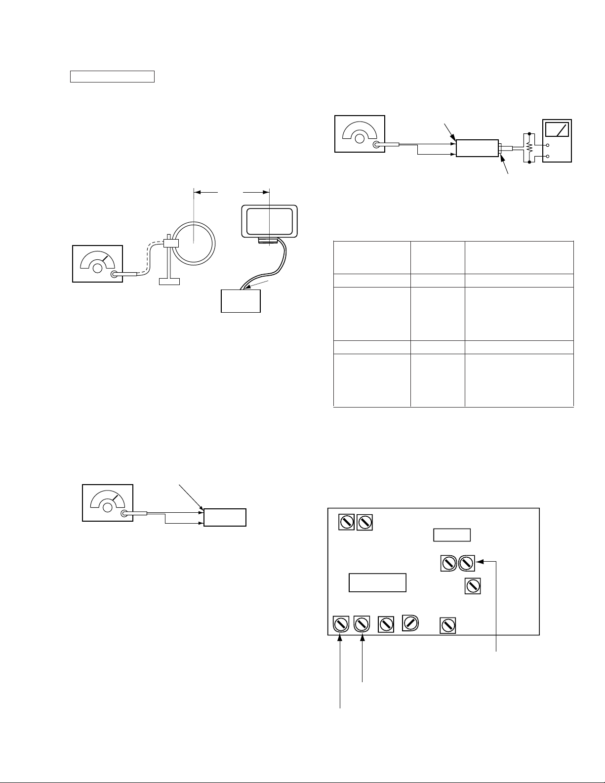
4-6. Laser Power Adjustment
Connection :
laser power mete
Optical pickup
objective lens
digital voltmete
BD (MD) board
TP (I+5V)
TP (IOP)
+
–
Adjusting Method :
1. Set the laser power meter on the objective lens of the optical pickup.
(When it cannot be set properly, press the 0 button or ) but-
ton and move the optical pickup.)
Connect the digital volt meter to TP (IOP) and TP (I+5V).
2. Rotate the JOG dial and display “LDPWR ADJUST”.
(Laser power : For adjustment)
3. Press the YES button twice and display “LD $ 4B = 3.5mW”.
4. Adjust RV102 of the BD (MD) board so that the reading of the
laser power meter becomes 3.4
+0.1
- 0
mW.
5. Press the YES button and display “LD $ 96 = 7.0mW”.
(Laser power : MO writing)
6. Check that the laser power meter and digital voltmeter readings
satisfy the specified value.
Specification :
Laser power meter reading : 7.0 ± 0.3 mW
Digital voltmeter reading : Optical pickup displayed value
± 10%
(Optical pickup label)
KMS210A
27X40
B0825
IOP = 82.5mA in this case
IOP (mA) = Digital voltmeter reading (mV) / 1(Ω)
7. Press the YES button and display “LD $ 0F = 0.7mW”.
(Laser power : MO reading)
8. Check that the laser power meter at this time satisfies the specified value.
Specification :
Laser power meter reading : 0.70 ± 0.1mW
9. Press the NO button and display “LDPWR ADJUST”, and stop
laser emission.
(The NO button is effective at all times to stop the laser emission.)
– 15 –
Page 16

6-7. T raverse Adjustment
Connection :
oscilloscope
BD (MD) board
TP (TEO)
TP (VC)
+
–
Adjusting Method :
1. Connect an oscilloscope to TP (TEO) and TP (VC) of the BD
(MD) board.
2. Load a MO disc (any available on the market).
3. Press the 0 button or ) button and move the optical pickup
outside the pit.
4. Rotate the JOG dial and display “EFBAL ADJUST”.
5. Press the YES button and display “EFBAL MO-W”.
(Laser power WRITE po wer/Focus servo ON/tracking servo OFF/
spindle (S) servo ON)
6. Adjust R V101 of the BD (MD) board so that the wa v eform of the
oscilloscope becomes the specified value.
(MO groove write power traverse adjustment)
(Traverse Wavefom)
A
VC
B
Specification : A = B
7. Press the YES button and display “EFB = $ MO-R”.
(Laser power : MO reading)
8. Rotate the JOG dial so that waveforms of the oscilloscope becomes the specified value.
(When the JOG dial is rotated, the
of “EFB = ” changes and
the waveform changes.) in this adjustment, waveform varies at
intervals of approx. 3%. Adjust the waveform so that the specified value is satisfied as much as possible.
(MO groove read power traverse adjustment)
(Traverse Wavefom)
11.Rotate the JOG dial until the waveforms of the oscilloscope moves
closer to the specified value.
In this adjustment, waveform varies at intervals of approx. 3%.
Adjust the waveform so that the specified value is satisfied as
much as possible.
(Traverse Wavefom)
A
VC
B
Specification : A = B
12.Press the YES button, display “EFB = SAVE ” for a moment
and save the adjustment results in the non-volatile memory.
Next “EFBAL CD” is displayed. The disc stops rotating automatically.
13.Press the MD § button and remove the MO disc.
14.Load the test disc TDYS-1.
15.Press the YES button and display “EFB =
CD ” . Servo is im-
posed automatically.
16.Rotate the JOG dial so that the waveforms of the oscilloscope
moves closer to the specified value.
In this adjustment, waveform varies at intervals of approx. 3%.
Adjust the waveform so that the specified value is satisfied as
much as possible.
(Traverse Wavefom)
A
VC
B
Specification : A = B
17.Press the YES button, display “EFB = $ SAVE” for a moment
and save the adjustment results in the non-volatile memory.
Next “EFBAL ADJUST” is displayed.
18.Press the MD § button and remove the test disc TDYS-1.
A
VC
B
Specification : A = B
9. Press the YES button, display “EFB = $ SAVE” for a moment
and save the adjustment results in the non-volatile memory.
Next “EFBAL MO-P” is displayed.
10.Press the YES button and display “EFB = $
MO-P”.
The optical pickup moves to the pit area automatically and servo
is imposed.
Note 1) Data will be erased during MO reading if a recorded disc is
used in this adjustment.
Note 2) If the traverse waveform is not clear, connect the oscillo-
scope as shown in the following figure so that it can be seen
more clearly.
oscilloscope
Ω
TP (TEO)
TP (VC)
330k
10pF
– 16 –
+
–
Page 17

6-8. Focus Bias Adjustment
Adjusting Method :
1. Load a continuously recorded disc (Refer to “6-4. Creating MO
Continuously Recorded Disc”.)
2. Rotate the JOG dial and display “CPLAY MODE”.
3. Press the YES button twice and display “CPLAY MID”.
4. Press the NO button when “C1 = AD = ” is displayed.
5. Rotate the JOG dial and display “FBIAS ADJUST”.
6. Press the YES button and display “ / a = ”.
The first four digits indicate the C1 error rate, the two digits after
[/] indicate ADER, and the 2 digits after [a =] indicate the focus
bias value.
7. Rotate the JOG dial in the clockwise direction and find the focus
bias value at which the C1 error rate becomes 220.
8. Press the YES button and display “ / b = ”.
9. Rotate the JOG dial in the counterclockwise direction and find
the focus bias value at which the C1 error rate becomes 220.
10.Press the YES button and display “ / c = ”.
11.Check that the C1 error rate is below 50 and ADER is 00.
Then press the YES button.
12.If the “( )” in “ - - ( )” is above 20, press the YES
button.
If below 20, press the NO button and repeat the adjustment from
step 2 again.
13.Press the NO button and press the MD § button to remove the
continuously recorded disc.
Note 1 : The relation between the C1 error and focus bias is as shown
in the following figure. Find points a and b in the following
figure using the above adjustment. The f ocal point position
c is automatically calculated from points a and b.
Note 2 : As the C1 error rate changes, perform the adjustment using
the average vale.
C1 error
220
Focus bias value
(F, BIAS)
bc b
6-9. Error Rate Check
6-9-1. CD Error Rate Check
Checking Method :
1. Load a test disc TDYS-1.
2. Rotate the JOG dial and display “CPLAY MODE”.
3. Press the YES button twice and display “CPLAY MID”.
4. “C1 =
AD = - -” is displayed.
5. Check that the C1 error is below 20.
6. Press the NO button, stop playback, press the MD § button, and
remove the test disc.
6-9-2. MO Error Rate Check
Checking Method :
1. Load a continuously recorded disc (Refer to “6-4. Creating MO
Continuously Recorded Disc”.)
2. Rotate the JOG dial and display “CPLAY MODE”.
3. Press the YES button twice and display “CPLAY MID”.
4. “C1 = AD = ”is displayed
5. If the C1 error rate is below 50, check that ADER is 00.
6. Press the NO button, stop playback, press the MD § button, and
remove the continuously recorded disc.
6-10. Focus Bias Check
Change the focus bias and check the focus tolerance amount.
Checking Method :
1. Load a continuously recorded disc (Refer to “6-4. Creating MO
Continuously Recorded Disc”.)
2. Rotate the JOG dial and display “CPLAY MODE”.
3. Press the YES button twice and display “CPLAY MID”.
4. Press the NO button when “C1 = AD = ” is displayed
5. Rotate the JOG dial and display “FBIAS CHECK”.
6. Press the YES button and display “
/ c = ”.
The first four digits indicate the C1 error rate, the two digits after
[/] indicate ADER, and the 2 digits after [c =] indicate the focus
bias value.
Check that the C1 error is below 50 and ADER is 00.
7. Press the YES button and display “ / b = ”.
Check that the C1 error is not below 220 and ADER is not above
00 every time.
8. Press the YES button and display “ / a = ”.
Check that the C1 error is not below 220 and ADER is not above
00 every time.
9. Press the NO button, next press the MD § button, and remove the
continuously recorded disc.
Note 1 : If the C1 error and ADER are abov e 00 at points a or b, the
focus bias adjustment may not have been carried out properly. Adjust perform the beginning again.
– 17 –
Page 18

6-11. Adjusting Points and Connecting Points
[BD (MD) BOARD] (Component side)
D101
[BD (MD) BOARD] (Conductor side)
(IOP)
(I+5V)
RV101
(VC)
RV102
IC191
IC101
(TEO)
IC121
– 18 –
Page 19
r
)
TUNER SECTION
As a front-end (TB1) is difficult to repair if faulty, replace it with
new one.
But AEP, UK, German, and Italian model are please note, however,
that the following adjustments are possible:
AM Section Adjustment
AM Tuned Indication Lighting Level Adjustment
Band : AM
Setting :
loop antenna
AM RF SSG
carrier frequency : 999kHz
Modulation : 400Hz 30%
60 cm
set
Procedure :
1. Set AM RF SSG output level to 81dBµ so that the input level
becomes 55dBµ.
2. Tune the set to 999kHz .
3. Adjust RV(AM TUNED LEVEL ADJUSTMENT) so that the
TUNED light up.
Adjustment Location : TB1 (TUNER board)
loop antenna of
accessories
AM ANTENNA
terminal (TM1)
FM Stereo Separation Adjustment
Setting :
FM RF SSG
FM ANTENNA terminal (TM1)
set
Carrier frequency : 98MHz
Output level : 1mV (60dB)
Modulation
Main (1kHz) : 33.75kHz dev. (45%)
Sub (1kHz) : 33.75kHz dev. (45%)
Pilot (19kHz) : 7.5kHz dev. (10%)
Procedure :
Turn the set to 98MHz.
FM stereo VTVM VTVM
signal generator connection reading (dB)
output channel
L-CH L-CH A
R-CH L-CH
Adjust RV (FM STEREO
SEPARATION ADJUSTMENT) for minimum reading.
R-CH R-CH C
L-CH R-CH
Adjust RV (FM STEREO
SEPARATION ADJUSTMENT) for minimum reading.
level mete
47k
Ω
J601 (LINE OUT)
B
D
+
–
FM Section Adjustment
FM Tuned Indication Lighting Level Adjustment
Band : FW
Setting :
FM RF SSG
carrier frequency : 98MHz
Modulation : 1kHz,75kHz deviation
FM ANTENNA terminal (TM1)
set
Procedure :
1. Supply a 17.8 µV (25dBµ) 98MHz signal to the ANTENNA ter-
minal.
2. Tune the set to 98MHz.
3. Adjust RV(FM TUNED LEVEL ADJUSTMENT) so that the
TUNED light up.
Adjustment Location : TB1 (TUNER board)
L-CH Stereo separation : A - B
R-CH Stereo separation : C - D
The separations of both channels should be equal.
Adjustment Location : TB1 (TUNER board)
[TB1 TUNER BOARD] (Conductor side )
IC
IC
RV (FM TUNED
LEVEL ADJUSTMENT
RV (AM TUNED LEVEL ADJUSTMENT)
RV (FM STEREO SEPARATION ADJUSTMENT)
– 19 –
Page 20

CD SECTION
s
NOTE :
1. CD Block basically constructed to operate without adjustment.
Therefore, check each item in order given.
2. Use YEDS-18 disc (3-702-101-01) unless otherwise indicated.
3. Use the oscilloscope with more than 10MΩ impedance.
4. Clean an object lens by an applicator with neutral detergent when
the signal level is low than specified value with the following
checks.
Focus Bias Adjustment
This adjustment is to be done when the optical block is replaced.
Adjustment procedure :
oscilloscope
(DC range)
BD (CD) board
TP (RF)
TP (VC)
1. Connect oscilloscope to test point TP (VC) and TP (RF) on BD
(CD) board.
2. Connect TP ADJ (IC301 @• pin) to ground with lead wire on Main
board.
3. Turned power switch ON. (Stop mode)
4. Put disc (YEDS-18) in and press the ^ button.
5. Press the ^ button (Tracking servo ON).
6. Adjust RV101 so that the oscilloscope waveform is as shown in
the figure below (eye pattern).
A good eye pattern means that the diamond shape ( ) in the center
of the waveform can be clearly distinguished.
7. After adjustment,remove the lead wire connected in step 2.
r RF signal reference waveform (eye pattern)
+
–
VOLT/DIV : 0.2V
TIME/DIV : 500n
1.3 ± 0.3Vp-p
2. Connect between test point TP (FOK) and GND by lead wire.
3. Turned Power switch on.
4. Put disc (YEDS-18) in and turned Power switch on again and
actuate the focus search. (actuate the focus search when disc table
is moving in and out.)
5. Check the oscilloscope waveform (S-curve) is symmetrical between A and B. And confirm peak to peak level within
2.4 ± 0.7Vp-p.
S-curve waveform
symmetry
A
within 2.4
B
±
0.7Vp-p
6. After check, remove the lead wire connected in step 2.
Note : r Try to measure several times to make sure that the ratio
of A : B or B : A is more than 10 : 7.
r T ake sweep time as long as possible and light up the bright
ness to obtain best waveform.
Adjustment Location : BD (CD) board. (see page 13)
RF Level Check
oscilloscope
BD (CD) board
TP (RF)
TP (VC)
Procedure :
1. Connect oscilloscope to test point TP (VC) and TP (RF) on BD
(CD) board.
2. Turned Power switch on.
3. Put disc (YEDS-18) in and press the ^ button.
4. Confirm that oscilloscope waveform is clear and check RF signal
level is correct or not.
Note :
Clear RF signal waveform means that the shape “◊” can be clearly
distinguished at the center of the waveform.
+
–
When observing the eye pattern, set the oscilloscope for A C range
and raise vertical sensitivity.
Adjustment Location : BD (CD) board. (see page 13)
S-Curve Check
oscilloscope
BD (CD) board
TP (FEO)
TP (VC)
+
–
Procedure :
1. Connect oscilloscope to test point TP (VC) and TP (FEO) on BD
(CD) board.
r RF signal waveform
VOLT/DIV : 200mV
TIME/DIV : 500ns
level : 1.3
Adjustment Location : BD (CD) board. (see page 13)
– 20 –
±
0.3Vp-p
Page 21

E-F Balance Check
oscilloscope
(DC range)
BD (CD) board
TP (TEO)
TP (VC)
+
–
Procedure :
1. Connect TP ADJ (IC301 @• pin) to ground with lead wire on Main
board.
2. Connect oscilloscope to test point TP (VC) and TP (TEO) on BD
(CD) board.
3. Turned Power switc h on.
4. Put disc (YEDS-18) in and press the ^ button.
5. Confirm that the osilloscope waveform is symmetrical on the
top and bottom in relation to 0V, and check this level.
Traverse waveform
A
0V
B
level : 300 ± 100mVp-p
Adjustment Location
[BD (CD) BOARD] (Conductor side)
RV103
IC104
RV101
TEO
VC
RF
IC101
FEO
RV102
GND
FOK
IC102
TE1
FE1
PCK
specified value : r
A–B
2 (A+B)
r
A+B = 300 ± 100mVp-p
X100 = less than ± 7%
6. Remove the lead wire connected in step 1.
Focus/Tracking Gain Adjustment (RV102, RV103)
This gain has a margin, so even if it is slightly off. There is no problem.
Therefore, do not perform, this adjustment.
Please note that it should be fixed to mechanical center position when
you moved and do not know original position.
– 21 –
Page 22

SECTION 7
IC101 RF AMP (CXA1981AR)
EXPLANATION OF IC TERMINALS
Pin No. Pin name I/O Description
1 VC O Output terminal for the center point voltage (+1.4V) generated.
2 – 7 A– F I Signal input from detector circuit in the optical pick-up block.
8 FI I Signal (–) input of the operational amplifier for F signal.
9 FO O Signal output of the operational amplifier for F signal.
10 PD I Front monitor. Connected to the photo diode.
11 APCREF I Input terminal for the setting of laser power.
12 TEMPI I Terminal for the connection to temperature sensor.
13 GND – Ground terminal.
14 AAPC O LD amplifier output terminal of APC circuit.
15 DAPC O Not used. (Open)
16 TEMPR O Output terminal of thr reference voltage for temperature sensor.
17 XRST I Reset signal input from the system controller (IC201). When reset : “L”
18 SWDT I Write data signal input from the system controller (IC201).
19 SCLK I Clock signal input from the system controller (IC201).
20 XLAT I Latch signal input from the system controller (IC201).
21 VREF O Reference voltage output. Not used this set (Open)
22 TENV O Not used. (Open)
23 THLD I Not used. (Connected to the VC)
24 VCC – Power supply terminal. (+5V)
25 TFIL I Not used. (Open)
26 TE O Tracking error signal output to CXD2535BR (IC121).
27 TLB I Input terminal of the adder signal to tracking error.
28 CSLED I Terminal for the sled error lowpass filter.
29 SE O Sled error signal output to CXD2535BR (IC121).
30 ADFM O FM signal output terminal of the ADIP.
31 ADIN I Input terminal by AC coupling is FM signal of the ADIP.
32 ADAGC I External capacitor connect terminal for AGC of the ADIP.
33 ADFG O ADIP double turned FM signal output to CXD2535BR (IC121). (22.05kHz±1kHz)
34 AUX O Sub signal output to CXD2535BR (IC121).
35 FE O Focus error signal output to CXD2535BR (IC121).
36 FLB I Not used. (Open)
37 ABCD O Light amount signal output to CXD2535BR (IC121).
38 BOTM O Light amount bottom hold signal output to CXD2535BR (IC121).
39 PEAK O Light amount peak hold signal output to CXD2535BR (IC121).
40 PFAGC I External capacitor connect terminal of AGC circuit for the RF.
41 RF O Playback EFM RF signal output to CXD2535BR (IC121).
42 ISET I Setting terminal for the internal circuit constant. 22kHz, BPF center frequency
43 AGCT I Input terminal by AC coupling is RF signal.
44 RFO O RF signal output terminal.
45 MORFI I Input terminal by AC coupling is RF signal of the MO.
46 MORFO O RF signal output terminal of the MO.
47,48 I,J I Signal input from detector circuit in the optical pick-up block.
– 22 –
Page 23

IC201 SYSTEM CONTROLLER (M37610MD-068FP)
Pin No. Pin name I/O Description
1 C. SET1 I Not used this set. (Fixed at “L”)
2 C. SET0 I Not used this set. (Fixed at “L”)
3 KEY3 I Key input terminal. Not used this set (Fixed at “L”)
4 – 6 KEY2–KEY0 I Key input terminal. Not used this set (Fixed at “L”)
7 I Not used this set. (Fixed at “L”)
8 XINT I Interruption status input from CXD2536R (IC271).
9 SENS I Internal status (SENSE) input from CXD2535BR (IC121).
10 SHCK I Track jump signal input from CXD2535BR (IC121).
11 AUBK I Audio bus signal input. (Not used this set)
12 S/A O Sircs remote controller/audio bus selection signal output. (Not used this set)
13 BEEP SW I Not used this set. (Fixed at “L”)
14 REC/OTHER O When recording :“L”, Other : “H” (Not used this set).
15 BEEP O Buzzer signal output. (Not used this set)
16 F. BIAS/C2 I Not used this set. (Fixed at “L”)
17 GND (CNVSS) – Ground terminal.
18 SYSTEM RST I System reset signal input. “H” after several hundred ms of “L” after power start-up.
19 XIN T I Not used this set. (Fixed at “L”)
20 XOUT T O Not used this set. (Fixed at “L”)
21 GND – Ground terminal.
22 XIN I 8MHz crystal oscillator input.
23 XOUT O 8MHz crystal oscillator output.
24 +5V – Power supply terminal. (+5V)
25 STB O Strobe signal output to the power supply circuit. When power ON :“H”, When standby : “L”
26, 27 MIC SW I Not used this set. (Fixed at “L”)
28 BUS OUT O Not used this set. (Fixed at “L”)
29 I Not used this set. (Fixed at “L”)
30, 31 LED2, LED1 I Not used this set. (Fixed at “L”)
32 LED0 O Not used this set. (Fixed at “L”)
33 C1 I Not used this set. (Fixed at “L”)
34 ADER I Not used this set. (Fixed at “L”)
35 N. C. I Not used this set. (Fixed at “L”)
36 MASTER/SLAVE I Not used this set. (Fixed at “H”)
37, 38 JOG1, JOG0 I Not used this set. (Fixed at “L”)
39 SDA I/O Backup memory (IC171) data bus.
40 SCL O Clock signal output to the Backup memory (IC171).
41 POWER DOWN I Power down detection input. Normally : “H” input
42 REMOCON I Remote control signal input. Not used this set (Fixed at “L”)
43 ATSY I
44 DQSY I
45 – 48 I Not used this set. (Fixed at “L”)
49 SCLK O Clock signal output to the serial bus.
–––
––––––––––
ATP address sync or sub-code Q sync (SCOR) input from CXD2535BR (IC121).
“L” every 13.3msec, Almost “H”
Input the U-bit CD format sub-code Q sync (SCOR) of the digital in from CXD2535BR (IC121).
“L” every 13.3msec, Almost “H”
– 23 –
Page 24

Pin No. Pin name I/O Description
50 SWDT O Write data signal output to the serial bus.
51 SRDT I Read data signal input to the serial bus.
52 I Connected to the pin %¡.
53 FLCLK O Serial clock signal output to the display driver (IC701). Not used this set (Fixed at “L”)
54 FLDATA O Serial data signal output to the display driver (IC701). Not used this set (Fixed at “L”)
55 FLCS O Chip select signal output to the display driver (IC701). Not used this set (Fixed at “L”)
56 I Not used. (Fixed at “L”)
57 TEST0 I Terminal for test. (Fixed at “L”)
58 TEST1 O Reset signal output to CXD2536R (IC271).
59, 60 I Not used. (Fixed at “L”)
61 AFAST I Not used this set. (Fixed at “L”)
62 16/18 I 16bit/18bit selector. “H” : 16bit
63 LDON O Laser ON/OFF control signal output.When laser ON : “H”
64 P/GROOVE I
65 FOK I Focus OK signal input from CXD2535BR (IC121). “H” is input when the focus is applied.
66 MON I Not used this set. (Input and the pull-down)
67 LOCK O Not used this set. (Output and the pull-down)
68 WRPWR O Laser power selection signal output to the optical pick-up block and CXD2535BR (IC121).
69 DIG RST O
70 DA RST O
71, 72 SCMD 1, SCMD 0 O Serial command control mode signal output to CXD2536R (IC271).
––––
PIT/GROOVE detection input.“H” : Disc for playing and TOC area.
Not used this set (Fixed at “L”)
Reset signal output to CXA1981R (IC101), CXD2535BR (IC121), and the motor driver
(IC151).When reset : “L”
Reset signal output to D/A converter (IC341) and the A/D converter (IC301).
When reset : “L”
Laser modulation selection signal output.
When playback power : “L”,When stop : “H”
When recording power :
73 MOD O
74 REC/PB O
Recording/playback selection signal output to CXD2535BR (IC121).
When recording : “H” ,When playback : “L”
0.5S
2S
75 WR/MN O Write/monitor mode selection signal output to CXD2536R (IC271).
76 SCTX O
Writing data transmission timing output to CXD2536R (IC271).
Used together with the magnetic field head ON/OFF output.
77 XLATCH O Latch signal output to the serial bus.
78 DFLATCH O Latch signal output to the D/A converter (IC341).
79 DFMUTE O Muting signal output. Not used this set. (Connected to the Ground)
– 24 –
Page 25

Pin No. Pin name I/O Description
80 AMUTE O Line out muting signal output.
81 LDOUT O Loading motor (M191) control output. *1
82 LDIN O Loading motor (M191) control output. *1
83 CHKIN I Detection signal input from the chucking in switch (S193). When chucking : “L”
84 INSW I
85 OUTSW I
86 PROTECT I
87 REFLECT I
88 LIMIT IN I
89 232C. 4 O UART data transmission request signal output to mPD78052G (IC301)
90 232C. 3 I UART data transmission reqeust signal input from mPD78052G (IC301)
91 232C. 2 I UART data input from mPD78052GC (IC301)
92 232C. 1 O UART data output to mPD78052GC (IC301)
93–96 O Not used (Fixed at “L”).
97 AVSS (AGND) – Ground terminal.
98 VREF (+5V) I Reference voltage input (+5V)
99 TIMER REC/PLAY I When timer recording : “H”, When timer playback : “L”,
100 INPUT SELECT I Analog/digital in selection signal input terminal
Detection signal input from the loading in switch (S192).
“L” at the position where the head descends, Others : “H”
Detection signal input from the loading out switch (S191).
“L” at the position of load out, Others : “H”
Rec proof detection signal input from the protect detector switch (S102-1).
When protect : “H”
Disc reflection rate detection signal input from the reflect detector switch (S102-2).
“H” : Low reflection rate disc
Detection signal input from the limit in switch (S101).
When sled limit in : “L”
Timer record /time playback/time OFF selection signal input terminal.
When timer OFF : Center point voltage (+2.5V) Not used this set (Fixed at “L”)
When analog in : “L”, When digital in : “H” Not used this set (Fixed at “L”)
* 1 Loading motor control
Mode
Terminal
LDIN pin *™ “H” “L” “H”
LDOUT pin *¡ “L” “H” “H”
IN OUT BRAKE
– 25 –
Page 26

IC271 SHCCK PROOF MEMORY CONTROLLER, ATRAC ENCODER/DECODER (CXD2536R)
Pin No. Pin name I/O Description
1 VDD – Power supply terminal. (+5V)
2 SWDT I Write data signal input from the system controller (IC201).
3 SCK I Serial clock signal input from the system controller (IC201).
4 XLAT I Serial latch signal input from the system controller (IC201).
5 SRDT O Read data signal output to the system controller (IC201).
6 SENSE O Internal status (SENSE) output to the system controller (IC201).
7 SCMD0 I Serial command control mode input from the system controller. (Fixed at “H”)
8 SCMD1 I Serial command control mode input from the system controller. (Fixed at “H”)
9 XINT O Interruption status output to the system controller (IC201).
10 RCPB I Record/playback selection signal input. Not used this set. (Fixed at “L”)
11 WRMN I Write/monitor mode selection signal input from the system controller (IC201).
12 TX –
13 VSS – Ground terminal.
14 SICK I Chip reserve terminal. (Fixed at “L”)
15 IDSL I Chip reserve terminal. (Fixed at “L”)
16 XILT I Chip reserve terminal. (Fixed at “H”)
17 XRST I Reset signal input from the system controller (IC201). When reset : “L”
18–21 TS0–TS3 I Test input terminal. (Fixed at “L”)
22 EXIR I Chip reserve terminal. (Fixed at “L”)
23 SASL I Single use the block selection. “L” : ATRAC, “H” : RAM Controller (Fixed at “L”)
24 SNGLE I
25 VSS – Ground terminal.
26 AIRCPB O
27 XRQ I/O XRQ signal input/output terminal of the ATRAC interface. Not used this set.
28 ADTO I/O Decoder data signal input/output terminal of the ATRAC. Not used this set.
29 ADTI I/O Encoder data signal input/output terminal of the ATRAC. Not used this set.
30 XALT I/O XALT signal input/output terminal of the ATRAC interface. Not used this set.
31 ACK I/O ACK signal input/output terminal of the ATRAC interface. Not used this set.
32 AC2 I/O Error data signal input/output terminal of the ATRAC interface. Not used this set.
33 LCHST I/O Lch Start data signal input/output terminal of the ATRAC interface. Not used this set.
34 EXE I/O EXE signal input/output terminal of the ATRAC interface. Not used this set.
35 MUTE I/O MUTE signal input/output terminal of the ATRAC interface. Not used this set.
36 OSCO O 45MHz clock oscillation output. (45MHz)
37 OSCI I 45MHz clock oscillation input. (45MHz)
38 VSS – Ground terminal.
39 ATT I/O ATT signal input/output terminal of the ATRAC interface. Not used this set.
40 F86 O 11.6msec timing signal output terminal of the ATRAC block. Not used this set.
41 DOUT O Monitor/audio decode data signal output to the D/A converter (IC281).
42 ADIN I Recoding data signal input from the D/A converter (IC261).
43 ABCK O Bit clock signal output to the A/D, D/A converter (IC261, 281).
44 ALRCK O L/R clock signal output to the A/D, D/A converter (IC261, 281).
45-47 SA2-SA0 O Address signal output. Not used this set (OPEN)
48,49 A11,A10 O Address signal output. Not used this set
Writing data transmission timing input from the system controller (IC201).
Used together with the magnetic field head ON/OFF output.
Normally fixed at “L”, Fixed at “H” when the ATRAC or RAM controller is single used.
(Fixed at “L”)
Record/playback mode signal output terminal of the ATRAC or external audio block.
Not used this set.
– 26 –
Page 27

Pin No. Pin name I/O Description
50 VSS – Ground terminal.
51 VDD – Power supply terminal. (+5V)
52– 55 A03– A00 O Address signal output to the RAM (IC222)
56– 60 A04– A08 O Address signal output to the RAM (IC222)
61 XOE O Output enable control signal output to the RAM (IC222).
62 XCAS O Column address strobe signal output to the RAM (IC222).
63 VSS – Ground terminal.
64 XCS O Chip select signal output. Not used this set
65 A09 O Address signal output to the RAM (IC222).
66 XRAS O Row address strobe signal output to the RAM (IC222).
67 XWE O Write enable control signal output to the RAM (IC222).
68,69 D1, D0 I/O RAM (IC222) data bus.
70,71 D2,D3 I/O RAM (IC222) data bus.
72–74 D4–D6 I/O Data bus. Not used this set (OPEN)
75 VSS – Ground terminal.
76 D7 I/O Data bus. Not used this set (OPEN)
77 ERR I/O
78 EXTC2R I
79 BUSY O BUSY signal output of the RAM access. Not used this set (OPEN)
80 EMP O Empty or before the full of the ATRAC data. (When DSC=ASC+1 : “H” ). Not used this set.
81 FUL O Full or before the empty of the ATRAC data. (When ASC=DSC+1 : “H” ). Not used this set.
82 EQL O Empty of the ATRACK data. (when DSC=ASC : “H” ). Not used this set.
83 MDLK O
84 CPSY O Interpolation sync signal output. Not used this set.
85 CTMD0 O DSC counter mode output. Not used this set.
86 CTMD1 O DSC counter mode output. Not used this set.
87 SPO O System clock (512Fs=22.5792MHz) signal output to CXD2535BR (IC121).
88 VSS – Ground terminal.
89 MDSY O Sync detection signal output of the main data. Not used this set.
90 LRCK I L/R clock (44.1kHz) signal input from CXD2535BR (IC121).
91 BCK I Bit clock (2.8224MHz) signal input from CXD2535BR (IC121).
92 C2PO I When playback : C2PO (“H”), When digital recording : D. IN-Vflag,
93 DATA I/O
94 DIDT I 16-bit data input terminal for the digital audio in from the CXD2535BR(IC121).
95 DODT O 16-bit data output terminal for the digital audio out from the CXD2535BR (IC121).
96 DIRCPB O
97 MIN I Defect ON/OFF selection signal input from CXD2535BR (IC121).
98 SPOSL I IN/OUT selection input terminal of the pin *¶. ( “L” : IN, “H” : OUT) (Fixed at “H”)
99 MCKT1 O Internal master clock signal output terminal of the RAM controller. Not used ths set.
100 VSS – Ground terminal.
Input/output terminal of the error (C2PO) data signal to the external RAM.
Not used this set (OPEN)
External RAM selection signal input for the error data writing.
(When “H” : External RAM) (Fixed at “L”).
Indicate the main/sub of the recording or playback data.
(When sub and linking : “H” , When the main : “L”). Not used this set.
C2PO (indicate the error mode of the data) signal input from CXD2535BR (IC121).
When analog recording : “L”
When recording : Record audio data signal output to CXD2535BR (IC121).
When playback : playback audio data signal input from CXD2535BR (IC121).
Disc drive, Record or playback mode output of the EFM encoder/decoder.
Not used this set (Open)
– 27 –
Page 28

IC301 MASTER CONTROL (µPD78058GC-243-3B9)
Pin No. Pin name I/O Description
1 LID SW I LID switch input (OPEN, CLOSE, SHUT switch).
2 MD RESET I Reset input for MD.
3 I CADY sensor input terminal.
4 AVSS – Ground.
5 LID-OPEN O LID motor control output (open direction).
6 LID CLS O LID motor control output (close direction).
7 – Not used.
8 DATA IN I Serial data input from MD.
9 DATA OUT O Serial data output to MD.
10 CTS I Clock input from 8 , 9 pin.
11 RTS O Clock output to 8 , 9 pin.
12 SDATA O Serial data output to FL driver.
13 SCK O Clock output to FL driver.
14 CS O Chip selector output to FL driver.
15 REST O Reset output to FL driver.
16 SUBQ I SUB “Q” input from CD.
17 OPEN – Not used.
18 SQCLK O SUB “Q” clock output to CD.
19 CCLOK O Master clock output to CD.
20 DATA O Data output to CD.
21 XLT O Latch output to CD.
22 DFLATCH O Latch output to CD digital filter.
23 FCSSW O output to Focus SW.
24 A MUTE – Not used.
25 BDRST O Reset output to CD.
26 CD POWER O CD Block Power ON/OFF. ( “H” : ACT )
27 SENS I Sens input from CD.
28 ADJ I Terminal for test mode. ( “L” : Test mode )
29 IN SW I LOAD IN Switch input. ( close )
30 OUT SW I LOAD OUT Switch input. ( open )
31 LOD IN O Loading Motor drive output. ( open direction )
32 LOD OUT O Loading Motor drive output. ( close direction )
33 VSS – Ground.
34 – Not used. ( open )
35 – Not used. ( open )
36 SYS POWER O System power ON / OFF control. ( “L” : power ON )
37 – Not used.
38 ST POWER O ST Power ON / OFF control. ( “L” : ST ON )
39 TAPE – Not used.
40 – Not used.
41 – Not used.
42 STEREO I Stereo Signal input from ST block.
43 TUNED I Tuned Signal input from ST block.
44 DATA IN I Serial data input from ST block.
45 DATA OUT O Serial data output to ST block.
46 CLOCK I/O Clock input / output of the ST block.
–––––
––––––––––––––––––––
––––––––––––––––––––––
––––––––––––––––––––
––––––––––
– 28 –
Page 29

Pin No. Pin name I/O Description
47 CE O Chip enable output to ST block.
48 CE O Chip enable output to IC101 ( CXA1946Q ).
49 CLOCK O Clock output to IC101 ( CXA1946Q ).
50 DATA O Serial data output to IC101 ( CXA1946Q ).
51 TA MUTE O Mute signal output to AMP. “L” : Mute
52 AUX ATT O Attenuation output for when AUX input. “L” : ATT
53 MIC DET – Not used.
54 CLEAR O Reset output to LED driver.
55 LATCH O Latch output to LED driver.
56 CLOCK O Clock output to LED driver.
57 DATA O Data output to LED driver.
58 SIRCS I SIRCS signal input terminal.
59 AC-DET I AC detection terminal.
60 CST I System reset terminal.
61 AUB I – Not used. ( Ground connection )
62 AUB O – Not used. ( Ground connection )
63 ENC I Input terminal from encoder.
64 ENC I Input terminal from encoder.
65 Not used.
66 FAN I FAN input terminal.
67 SCOR I SCOR input from BD.
68 VDD – Power supply. ( +5 V )
69 X2 O MICOM clock output terminal. ( 5.0 MHz )
70 X1 I MICOM clock input terminal. ( 5.0 MHz )
71 GND – Ground.
72 XT2 O Clock output for timer. ( 3.0 kHz )
73 XT1 I Clock input for timer. ( 3.0 kHz )
74 AVDD – Power supply for Analog. ( +5 V )
75 AVREFO – Reference Voltage output for Analog. ( +5 V )
76 K0 I Key input.
77 K1 I Key input.
78 K2 I Key input.
79 K3 I Key input.
80 VER I Input terminal for Virsion Select.
– 29 –
Page 30

Page 31

Page 32

Page 33

Page 34

Page 35

Page 36

Page 37

Page 38

Page 39

Page 40

Page 41

Page 42

Page 43

Page 44

Page 45

SECTION 9
EXPLODED VIEWS
NOTE :
r
-XX, -X mean standardized parts, so they may
have some difference from the original one.
r
Items marked “ * ”are not stocked since they
are seldom required for routine service. Some
delay should be anticipated when ordering these
items.
9-1. CABINET SECTION
8
6
5
4
3
2
r
The mechanical parts with no reference number in the exploded views are not supplied.
r
Hardware (# mark) list and accessories and
packing materials are given in the last of this
parts list.
r
Abbreviation
CND : Canadian SP : Singapore
HK : Hong Kong G : German
IT : Italian
7
9
9
11
#1
10
#3
12
The components identified by mark !
or dotted line with mark ! are critical
for safety.
Replace only with part number specified.
Les composants identifiés par une
marque !sont critiques pour la sécurité.
Ne les remplacer que par une pièce
portant le numéro spécifié.
8
#2
#1
#2
#2
#6
22
13
14
15
17
(including 12)
1
16
not supplied
#1
#1
#1
#18
#1
Ref. No. Part No. Description Remark Ref. No. Part No. Description Remark
––––––– ––––––– –––––––––– ––––––– ––––––– ––––––– –––––––––– ––––––
1 X-4947-203-1 CASE (TOP) ASSY (US,CND)
1 X-4947-204-1 CASE (TOP) ASSY (AEP,UK,G,IT)
* 1 X-4947-205-1 CASE (TOP) ASSY (HK,SP)
* 2 1-661-325-11 HP BOARD
* 3 1-661-324-11 SWITCH (L) BOARD
4 4-980-513-01 PLATE, INDICATION
5 X-4947-046-1 BUTTON (POWER) ASSY
6 X-4947-044-1 BUTTON (MODE) ASSY
7 4-980-512-01 PLATE, ORNAMENTAL
8 4-982-457-01 SCREW, HEXAGON HOLE TAPPING
#1
11 X-4947-291-1 KNOB (JOG) ASSY
12 4-942-567-01 EMBLEM (NO.4), SONY
13 X-4947-045-1 BUTTON (BAND) ASSY
* 14 4-980-506-01 PLATE (T BACK), ORNAMENTAL
15 1-777-137-11 WIRE (FLAT TYPE) (11CORE)
* 16 1-661-323-11 SWITCH (R) BOARD
17 4-951-620-01 SCREW (2.6X8), +BVTP
* 18 1-661-329-11 IR BOARD
19 4-981-608-11 WASHER, SLIT
20 X-4946-857-1 ROTOR ASSY
18
19
17
20
21
17
9 4-980-519-01 INDICATOR (FUN)
10 X-4947-047-1 BUTTON (VOL) ASSY
21 X-4946-856-1 PLATE (JOG) ASSY
22 4-983-312-01 BRACKET (T BACK)
– 79 –
Page 46

9-2. CHASSIS SECTION-1
59
#4
#4
60
61
62
#1
71
#4
FL501
54
55
53
#4
52
56
#4
54
#4
51
58
57
#2
#5
#2
#18
63
FAN801
not
supplied
#4
64
S801
#4
67
65
68
F801
F802
68
#2
#4
T801
70
69
not
supplied
#2
66
Ref. No. Part No. Description Remark Ref. No. Part No. Description Remark
––––––– ––––––– –––––––––– ––––––– ––––––– ––––––– –––––––––– ––––––
* 51 4-982-455-01 HOLDER, PC BOARD
* 52 1-661-322-11 DISPLAY BOARD
* 53 4-980-523-01 HOLDER (FL)
* 54 4-955-901-01 CUSHION (FL)
* 55 4-980-522-01 FILTER
* 56 1-661-333-11 TUNER BOARD
* 57 A-4390-522-A AMP BOARD, COMPLETE (US)
* 57 A-4390-538-A AMP BOARD, COMPLETE (AEP,G,IT)
* 57 A-4390-554-A AMP BOARD, COMPLETE (HK,SP)
* 57 A-4390-719-A AMP BOARD, COMPLETE (CND)
* 57 A-4390-735-A AMP BOARD, COMPLETE (UK)
58 1-777-033-11 WIRE (FLAT TYPE) (19 CORE)
59 1-773-004-11 WIRE (FLAT TYPE) (15 CORE)
* 60 A-4390-518-A MAIN BOARD, COMPLETE (US)
* 60 A-4390-534-A MAIN BOARD, COMPLETE (AEP,G,IT)
* 60 A-4390-550-A MAIN BOARD, COMPLETE (HK,SP)
* 60 A-4390-715-A MAIN BOARD, COMPLETE (CND)
* 60 A-4390-731-A MAIN BOARD, COMPLETE (UK)
61 1-777-291-11 WIRE (FLAT TYPE) (21 CORE)
62 1-769-974-11 WIRE (FLAT TYPE) (13 CORE)
63 1-773-106-11 WIRE (FLAT TYPE) (19 CORE)
64 1-773-117-11 WIRE (FLAT TYPE) (19 CORE)
* 65 1-661-328-11 TERMINAL BOARD
* 66 1-661-332-11 TRANSFORMER BOARD
* 67 1-661-331-11 AC BOARD
68 1-533-293-11 FUSE HOLDER
* 69 4-888-798-11 BUSHING, RUBBER
* 70 4-983-696-01 COLLAR
* 71 4-617-314-01 CLAMP
! F801 1-533-296-11 FUSE,GLASS CYLINDRICAL (2A 125V)(US,CND)
! F801 1-532-259-00 FUSE, TIME LAG (T1.6AL 250V)(SP,HK)
! F802 1-532-215-00 FUSE, TIME LAG (T0.8AL 250V)
FAN801 1-698-651-11 FAN, D.C.
FL501 1-517-520-11 INDICATOR TUBE, FLUORESCENT
! S801 1-572-675-11 SWITCH, POWER VOLTAGE CHANGE
! T801 1-429-661-11 TRANSFORMER, POWER (AEP,UK,G,IT)
! T801 1-429-662-11 TRANSFORMER, POWER (SP,HK)
! T801 1-429-663-11 TRANSFORMER, POWER (US,CND)
The components identified by mark !
or dotted line with mark ! are critical
for safety.
Replace only with part number specified.
Les composants identifiés par une
marque !sont critiques pour la sécurité.
Ne les remplacer que par une pièce
portant le numéro spécifié.
(AEP,UK,G,IT,SP,HK)
– 80 –
Page 47

9-3. CHASSIS SECTION-2
115
#6
131
M701
114
#4
113
107
108
129
128
not
supplied
#17
106
126
132
#4
105
#17
111
104
103
130
133
112
134
#6
109
102
#4
#2
110
CDM13C-5BD19
134
not supplied
#2
#4
MDM-2ER
#2
not supplied
124
136
119
not
supplied
#3
#3
#4
#2
118
#3
117
CNP801
125
AEP, G,
IT,HK,SP
model
HK
model
CNP801
120
not supplied
Ver 1.2
CNP801
US,CND
model
UK
model
101
not supplied
127
Ref. No. Part No. Description Remark Ref. No. Part No. Description Remark
––––––– ––––––– –––––––––– ––––––– ––––––– ––––––– –––––––––– ––––––
101 X-4946-828-1 LID ASSY
* 102 1-661-335-11 SENSOR BOARD
* 103 4-980-529-01 HOLDER (SENSOR)
104 4-980-520-01 PANEL, CD
105 4-981-608-11 WASHER, SLIT
106 4-980-496-01 GEAR (CAM)
* 107 4-980-492-01 PLATE (CL)
* 108 X-4946-826-1 CHASSIS (LD) ASSY
109 4-980-495-01 GEAR (C)
110 4-981-608-01 WASHER, SLIT
* 111 X-4946-830-1 PLATE (OP) ASSY
112 4-965-659-01 SCREW (+B 2X2.2)
113 4-982-456-01 SPRING, TENSION
* 114 1-661-327-11 SWITCH (LID) BOARD
* 115 1-661-326-11 MOTOR (LID) BOARD
116 4-984-379-01 CUSHION (FOOT)
117 1-777-291-11 WIRE (FLAT TYPE) (21 CORE)
* 118 A-4390-532-A DIGITAL BOARD, COMPLETE (US)
* 118 A-4390-548-A DIGITAL BOARD, COMPLETE (AEP,G,IT)
* 118 A-4390-564-A DIGITAL BOARD, COMPLETE (HK,SP)
* 118 A-4390-729-A DIGITAL BOARD, COMPLETE (CND)
* 118 A-4390-745-A DIGITAL BOARD, COMPLETE (UK)
119 4-924-098-21 HOLDER, PC BOARD
* 120 3-703-244-00 BUSHING (2104), CORD
121 4-981-393-01 FOOT
122 3-531-576-11 RIVET
* 123 4-980-505-01 CASE (BOTTOM)
124 1-769-118-11 WIRE (FLAT TYPE) (30 CORE)
123
!125 1-770-019-11 ADAPTOR, CONVERSION PLUG 3P(HK)
* 126 4-983-700-01 CUSHION (L)
* 128 4-983-697-01 PLATE (LD)
* 129 4-983-708-01 RUBBER (C)
* 130 4-983-703-01 CUSHION (T)
* 131 4-983-705-01 RUBBER
* 132 4-983-702-11 CUSHION (M)
* 133 4-983-701-01 CUSHION (B)
* 134 4-983-707-01 RUBBER (B)
! CNP801 1-575-651-31 CORD, POWER (AEP,G,IT,SP,HK)
! CNP801 1-775-789-11 CORD, POWER (US,CND)
! CNP801 1-696-570-21 CORD, POWER (UK)
The components identified by mark !
or dotted line with mark ! are critical
for safety.
Replace only with part number specified.
116
not supplied
#19
127 4-949-303-41 SPACER
136 1-769-119-11 WIRE (FLAT TYPE) (18 CORE)
M701 X-4947-281-1 LID MOTOR,ASSY
#2 7-685-873-09 SCREW +BVTT 3X10 (S)
#3 7-685-871-01 SCREW +BVTT 3X6 (S)
#4 7-685-646-79 SCREW +BVTP 3X8 TYPE2 N-S
#6 7-685-132-19 SCREW +BTP 2.6X5 TYPE2 N-S
#17 7-685-546-19 SCREW +BTP 3X8 TYPE2 N-S
#18 7-685-874-09 SCREW +BVTT 3X12 (S)
#19 7-623-422-07 LW3, TYPE B
#18
122
Les composants identifiés par une
marque !sont critiques pour la sécurité.
Ne les remplacer que par une pièce
portant le numéro spécifié.
121
– 81 –
Page 48

9-4. MD MECHANISM SECTION
(MDM-2ER)
157
154
189
156
155
188
151
152
153
186
158
189
165
#9
189
164
188
151
166
160
161
162
163
#10
185
#8
not supplied
187
190
#10
173
174
152
153
169
170
152
152
153
167
168
153
MBU-2B
#7
#8
171
#1
#7
M191
172
184
183
180
182
175
176
177
178
179
181
not supplied
Ref. No. Part No. Description Remark Ref. No. Part No. Description Remark
––––––– ––––––– –––––––––– ––––––– ––––––– ––––––– –––––––––– ––––––
151 4-983-100-01 COLLAR (DAMPER)
152 4-967-671-01 INSULATOR (MD)
153 4-967-673-01 SPRING, COMPRESSION
154 4-967-668-01 SPRING (UDL), TORSION
155 4-967-667-01 LEVER (UDL)
156 4-977-610-01 GEAR (BD-B)
157 X-4945-069-1 CAM ASSY
158 4-967-656-01 BELT (BD)
160 4-967-637-01 LEVER (SLM)
161 4-984-426-01 SPRING (SLM), TORSION
162 4-968-273-01 SPRING (OWH), TORSION
163 4-968-272-01 LEVER (OWH)
164 4-977-609-01 GEAR (BD-A)
165 4-957-794-01 PULLEY (GEAR 1)
* 166 X-4945-068-1 BASE (BD) ASSY
167 4-967-669-01 LEVER (UDR)
168 4-967-670-01 SPRING (UDR), TORSION
169 4-979-400-01 LEVER (DOOR)
170 4-970-710-01 SPRING, COMPRESSION
* 171 1-653-411-11 DETECTION SW BOARD
* 172 1-653-412-11 MOTOR BOARD
173 A-4672-087-A BRACKET (LVO) ASSY
174 X-4947-136-2 HOLDER ASSY
175 4-968-919-11 WASHER, STOPPER
176 4-967-646-01 SPRING (SHT), TORSION
177 4-967-645-01 LEVER (SHT)
178 4-983-106-02 SPRING (LM), TORSION
179 4-967-639-01 LEVER (LM)
180 4-968-919-01 WASHER, STOPPER
181 4-967-641-01 LEVER (L)
182 4-967-642-01 SPRING (L), TORSION
183 4-982-040-01 LEVER (LOCK)
184 4-982-099-01 SPRING (LOCK), TORSION
185 4-971-743-02 SPRING, TENSION
186 4-933-134-01 SCREW (+PTPWH M2.6X6)
* 187 X-4945-872-1 SLIDER (M) ASSY
188 4-972-910-01 SCREW (2.6X18), +B
189 7-621-770-67 SCREW +PWH 2.6X6
190 7-621-255-25 SCREW +PTT 2X4 (S)
M191 A-4660-646-A MOTOR (LOADING) ASSY
180
180
– 82 –
Page 49

9-5. BASE UNIT SECTION (MD)
(MBU-2)
S102
not
supplied
not supplied
#12
201
#12
#11
#12
202
HR901
not supplied
#11
M102
204
205
207
M101
206
208
Ref. No. Part No. Description Remark Ref. No. Part No. Description Remark
––––––– ––––––– –––––––––– ––––––– ––––––– ––––––– –––––––––– ––––––
* 201 1-634-461-11 LOADING BOARD
202 4-967-675-01 GEAR (SL-A)
204 4-967-676-01 GEAR (SL-B)
205 4-967-677-01 GEAR (SL-C)
206 4-967-678-01 SHAFT (OP)
! 207 8-583-009-11 OPTICAL PICK-UP KMS-210A/J-N (MD)
* 208 A-4673-809-A BD(MD)BOARD, COMPLETE
HR901 1-500-304-21 HEAD, OVER LIGHT (RF322-74A)
M101 A-4660-651-A MOTOR (SLED) ASSY
M102 A-4660-650-A CHASSIS ASSY, BU
S102 1-762-148-11 SWITCH, PUSH (2 KEY)
(PROTECT/REFLECT SWITCH)
The components identified by mark !
or dotted line with mark ! are critical
for safety.
Replace only with part number specified.
– 83 –
Les composants identifiés par une
marque !sont critiques pour la sécurité.
Ne les remplacer que par une pièce
portant le numéro spécifié.
Page 50

9-6. CD MECHANISM SECTION-1
(CDM-5BD19)
261
#4
#4
257
not supplied
262
#15
258
#14
254
S292
269
268
253
252
251
256
#15
255
M903
260
265
S291
266
not supplied
259
#13
#4
264
263
265
270
266
267
Ref. No. Part No. Description Remark Ref. No. Part No. Description Remark
––––––– ––––––– –––––––––– ––––––– ––––––– ––––––– –––––––––– ––––––
251 4-967-679-01 SPRING (OP), LEAF
252 4-927-654-01 WASHER (LIMITER)
253 3-659-338-00 SPRING, COMPRESSION
254 4-929-764-01 SHAFT (TABLE GUIDE)
255 4-927-620-01 GEAR (P)
256 4-944-006-11 BEARING
257 4-927-628-01 GEAR (C)
258 4-927-649-01 BELT
259 4-929-724-01 PULLEY (B)
260 X-4947-265-1 ARM ASSY, SWING
261 4-944-012-01 TABLE, DISC
262 A-4604-752-A HOLDER (MG) ASSY
* 263 4-917-583-21 BRACKET, YOKE
* 264 X-4946-208-2 CHASSIS (MD) ASSY
265 4-933-134-01 SCREW (+PTPWH M2.6X6)
266 4-958-593-01 SPRING (BU), COMPRESSION
267 4-929-747-01 HOLDER (BU)
268 4-929-727-01 CAM (A)
269 4-929-729-01 CAM (B)
270 1-777-033-11 WIRE (FLAT TYPE) (19 CORE)
M903 A-4608-362-A MOTOR (L)ASSY (LOADING)
S291 1-571-924-11 SWITCH, LEAF (LOAD OUT)
S292 1-571-924-11 SWITCH, LEAF (LOAD IN)
– 84 –
Page 51

9-7. CD MECHANISM SECTION-2
(CDM-5BD19)
304
305
306
307
r
A
#16
304
M104
(including rA)
303
308
M103
301
Ref. No. Part No. Description Remark Ref. No. Part No. Description Remark
––––––– ––––––– –––––––––– ––––––– ––––––– ––––––– –––––––––– ––––––
301 4-951-620-01 SCREW (2.6X8), +BVTP
* 302 A-4673-402-A BD (CD) BOARD, COMPLETE
303 4-917-565-01 SHAFT, SLED
304 4-951-940-01 INSULATOR (BU)
! 305 8-848-367-11 OPTICAL PICK-UP KSS-213B/K-N (CD)
302
306 1-769-069-11 WIRE (FLAT TYPE) (16 CORE)
307 4-917-567-01 GEAR (M)
308 4-917-564-01 GEAR (P), FLATNESS
M103 X-4917-504-1 MOTOR, ASSY(CD)(SLED MOTOR)
M104 X-4917-523-4 MOTOR, ASSY(CD)(SPINDLE MOTOR)
The components identified by mark !
or dotted line with mark ! are critical
for safety.
Replace only with part number specified.
– 85 –
Les composants identifiés par une
marque !sont critiques pour la sécurité.
Ne les remplacer que par une pièce
portant le numéro spécifié.
Page 52

AC
AMP
SECTION 10
ELECTRICAL PARTS LIST
NOTE :
r
Due to standardization, replacements in the
parts list may be different from the parts specified in the diagrams or the components used on
the set.
r
-XX, -X mean standardized parts, so they may
have some difference from the original one.
r
RESISTORS
All resistors are in ohms
METAL : Metal-film resistor
METAL OXIDE :Metal oxide-film resistor
F : nonflammable
r
Items marked “ * ”are not stocked since they
are seldom required for routine service. Some
delay should be anticipated when ordering these
items.
Ref. No. Part No. Description Remark Ref. No. Part No. Description Remark
––––––– ––––––– –––––––––– ––––––– ––––––– ––––––– –––––––––– ––––––
* 1-661-331-11 AC BOARD
*********
1-533-293-11 FUSE HOLDER
< CAPACITOR >
! C833 1-115-377-61 CERAMIC 3300PF 20% 250V
! C834 1-115-377-61 CERAMIC 3300PF 20% 250V
! C837 1-115-377-61 CERAMIC 3300PF 20% 250V
r
SEMICONDUCTORS
In each case, u : µ , for example :
uA.... : µ A.... , uPA.... : µ PA....
uPB.... : µ PB.... , uPC.... : µ PC....
uPD.... : µ PD....
r
CAPACITORS
uF : µ F
r
COILS
uH : µ H
r
Abbreviation
CND : Canadian SP : Singapore
HK : Hong Kong G : German
IT : Italian
C902 1-162-282-31 CERAMIC 100PF 10% 50V
C903 1-126-964-11 ELECT 10uF 20% 50V
C904 1-126-967-11 ELECT 47uF 20% 50V
C905 1-126-052-11 ELECT 100uF 20% 50V
C906 1-126-964-11 ELECT 10uF 20% 50V
C907 1-126-964-11 ELECT 10uF 20% 50V
C908 1-136-165-00 FILM 0.1uF 5% 50V
C909 1-136-165-00 FILM 0.1uF 5% 50V
C921 1-126-923-11 ELECT 220uF 20% 10V
The components identified by mark !
or dotted line with mark ! are critical
for safety.
Replace only with part number specified.
Les composants identifiés par une
marque !sont critiques pour la sécurité.
Ne les remplacer que par une pièce
portant le numéro spécifié.
When indicating parts by reference
number, please include the board.
< CONNECTOR >
CN801 1-564-321-00 PIN, CONNECTOR 2P
* CN802 1-564-687-11 PIN, CONNECTOR 3P
< FUSE >
! F801 1-533-296-11 FUSE,GLASS CYLINDRICAL (2A 125V)(US,CND)
! F801 1-532-259-00 FUSE, TIME LAG (T1.6AL 250V)(SP,HK)
! F802 1-532-215-00 FUSE, TIME LAG (T0.8AL 250V)
(AEP,UK,G,IT,SP,HK)
< LINE FILTER >
! LF801 1-411-910-11 TRANSFORMER, LINE FILTER
< SWITCH >
! S801 1-572-675-11 SWITCH, POWER VOLTAGE CHANGE
(VOLTAGE SELECTOR)(SP,HK)
************************************************************
* A-4390-522-A AMP BOARD, COMPLETE (US)
* A-4390-538-A AMP BOARD, COMPLETE (AEP,G,IT)
* A-4390-554-A AMP BOARD, COMPLETE (SP,HK)
* A-4390-719-A AMP BOARD, COMPLETE (CND)
* A-4390-735-A AMP BOARD, COMPLETE (UK)
********************
C922 1-124-903-11 ELECT 1uF 20% 50V
C923 1-126-964-11 ELECT 10uF 20% 50V
C941 1-124-903-11 ELECT 1uF 20% 50V
C951 1-126-964-11 ELECT 10uF 20% 50V
C952 1-162-282-31 CERAMIC 100PF 10% 50V
C953 1-126-964-11 ELECT 10uF 20% 50V
C954 1-126-967-11 ELECT 47uF 20% 50V
C955 1-126-052-11 ELECT 100uF 20% 50V
C956 1-164-159-21 CERAMIC 0.1uF 50V
C957 1-126-964-11 ELECT 10uF 50V
C958 1-136-165-00 FILM 0.1uF 5% 50V
C959 1-136-165-00 FILM 0.1uF 5% 50V
< CONNECTOR >
CN901 1-564-511-11 PLUG, CONNECTOR 8P
CN902 1-770-726-11 CONNECTOR, BOARD TO BOARD 6P
< DIODE >
D901 8-719-987-63 DIODE 1N4148M
D951 8-719-987-63 DIODE 1N4148M
< IC >
IC901 8-749-900-96 IC STK-4142MK2
< CAPACITOR >
C901 1-126-964-11 ELECT 10uF 20% 50V
< TRANSISTOR >
Q901 8-729-140-84 TRANSISTOR 2SC1841-PAFAEA
Q921 8-729-620-05 TRANSISTOR 2SC2603-EF
– 86 –
Page 53

AMP
Ref. No. Part No. Description Remark Ref. No. Part No. Description Remark
––––––– ––––––– –––––––––– ––––––– ––––––– ––––––– –––––––––– ––––––
Q922 8-729-620-05 TRANSISTOR 2SC2603-EF
Q923 8-729-620-05 TRANSISTOR 2SC2603-EF
Q924 8-729-119-76 TRANSISTOR 2SA1175-HFE
! R957 1-217-637-00 FUSIBLE 1 5% 1/4W F
! R959 1-212-881-11 FUSIBLE 100 5% 1/4W F
! R960 1-217-151-00 METAL PLATE 0.22 F
BD (CD)
Q925 8-729-620-05 TRANSISTOR 2SC2603-EF
Q931 8-729-620-05 TRANSISTOR 2SC2603-EF
Q932 8-729-422-73 TRANSISTOR UN4212
Q941 8-729-620-05 TRANSISTOR 2SC2603-EF
Q951 8-729-140-84 TRANSISTOR 2SC1841-PAFAEA
< RESISTOR >
R901 1-249-417-11 CARBON 1K 5% 1/4W
R902 1-249-438-11 CARBON 56K 5% 1/4W
R903 1-249-415-11 CARBON 680 5% 1/4W
R904 1-249-438-11 CARBON 56K 5% 1/4W
R905 1-260-103-11 CARBON 2.2K 5% 1/2W
R906 1-260-103-11 CARBON 2.2K 5% 1/2W
R907 1-260-099-11 CARBON 1K 5% 1/2W
R908 1-260-099-11 CARBON 1K 5% 1/2W
! R909 1-212-881-11 FUSIBLE 100 5% 1/4W F
! R910 1-217-151-00 METAL PLATE 0.22 F
R911 1-249-417-11 CARBON 1K 5% 1/4W
R912 1-249-431-11 CARBON 15K 5% 1/4W
R913 1-249-441-11 CARBON 100K 5% 1/4W
R914 1-260-076-11 CARBON 10 5% 1/2W
R921 1-249-438-11 CARBON 56K 5% 1/4W
R922 1-249-437-11 CARBON 47K 5% 1/4W
R923 1-249-441-11 CARBON 100K 5% 1/4W
R924 1-249-429-11 CARBON 10K 5% 1/4W
R925 1-249-441-11 CARBON 100K 5% 1/4W
R926 1-249-429-11 CARBON 10K 5% 1/4W
R927 1-249-441-11 CARBON 100K 5% 1/4W
R928 1-249-441-11 CARBON 100K 5% 1/4W
R929 1-249-429-11 CARBON 10K 5% 1/4W
R930 1-249-441-11 CARBON 100K 5% 1/4W
R931 1-249-429-11 CARBON 10K 5% 1/4W
R932 1-249-429-11 CARBON 10K 5% 1/4W
R933 1-249-439-11 CARBON 68K 5% 1/4W
R934 1-249-441-11 CARBON 100K 5% 1/4W
R935 1-249-441-11 CARBON 100K 5% 1/4W
R941 1-249-429-11 CARBON 10K 5% 1/4W
R942 1-249-441-11 CARBON 100K 5% 1/4W
R943 1-247-807-31 CARBON 100 5% 1/4W
R944 1-249-437-11 CARBON 47K 5% 1/4W
R945 1-249-437-11 CARBON 47K 5% 1/4W
R946 1-249-441-11 CARBON 100K 5% 1/4W
R947 1-249-429-11 CARBON 10K 5% 1/4W
R951 1-249-417-11 CARBON 1K 5% 1/4W
R952 1-249-438-11 CARBON 56K 5% 1/4W
R953 1-249-415-11 CARBON 680 5% 1/4W
R954 1-249-438-11 CARBON 56K 5% 1/4W
R955 1-260-103-11 CARBON 2.2K 5% 1/2W
R956 1-260-103-11 CARBON 2.2K 5% 1/2W
R961 1-249-417-11 CARBON 1K 5% 1/4W
R962 1-249-431-11 CARBON 15K 5% 1/4W
R963 1-249-441-11 CARBON 100K 5% 1/4W
R964 1-260-076-11 CARBON 10 5% 1/2W
< THERMISTOR >
TH931 1-807-796-11 THERMISTOR
************************************************************
* A-4673-402-A BD(CD) BOARD, COMPLETE
**********************
< CAPACITOR >
C101 1-126-607-11 ELECT CHIP 47uF 20% 4V
C102 1-163-275-11 CERAMIC CHIP 0.001uF 5% 50V
C103 1-164-346-11 CERAMIC CHIP 1uF 16V
C105 1-163-038-91 CERAMIC CHIP 0.1uF 25V
C106 1-164-695-11 CERAMIC CHIP 0.0022uF 5% 50V
C107 1-164-695-11 CERAMIC CHIP 0.0022uF 5% 50V
C108 1-164-232-11 CERAMIC CHIP 0.01uF 50V
C109 1-164-232-11 CERAMIC CHIP 0.01uF 50V
C110 1-163-989-11 CERAMIC CHIP 0.033uF 10% 25V
C111 1-163-038-91 CERAMIC CHIP 0.1uF 25V
C112 1-163-038-91 CERAMIC CHIP 0.1uF 25V
C113 1-164-695-11 CERAMIC CHIP 0.0022uF 5% 50V
C114 1-164-005-11 CERAMIC CHIP 0.47uF 25V
C115 1-126-607-11 ELECT CHIP 47uF 20% 4V
C116 1-163-016-00 CERAMIC CHIP 0.0039uF 10% 50V
C117 1-164-005-11 CERAMIC CHIP 0.47uF 25V
C118 1-107-823-11 CERAMIC CHIP 0.47uF 10% 16V
C119 1-163-038-91 CERAMIC CHIP 0.1uF 25V
C120 1-135-201-11 TANTALUM CHIP 10uF 20% 4V
C121 1-163-038-91 CERAMIC CHIP 0.1uF 25V
C122 1-164-232-11 CERAMIC CHIP 0.01uF 50V
C123 1-163-038-91 CERAMIC CHIP 0.1uF 25V
C124 1-126-607-11 ELECT CHIP 47uF 20% 4V
C125 1-164-232-11 CERAMIC CHIP 0.01uF 50V
C126 1-163-038-91 CERAMIC CHIP 0.1uF 25V
C127 1-164-695-11 CERAMIC CHIP 0.0022uF 5% 50V
C128 1-163-135-00 CERAMIC CHIP 560PF 5% 50V
C129 1-163-038-91 CERAMIC CHIP 0.1uF 25V
C130 1-164-336-11 CERAMIC CHIP 0.33uF 25V
C131 1-163-038-91 CERAMIC CHIP 0.1uF 25V
C132 1-163-037-11 CERAMIC CHIP 0.022uF 10% 25V
C133 1-163-145-00 CERAMIC CHIP 0.0015uF 5% 50V
C134 1-164-346-11 CERAMIC CHIP 1uF 16V
C135 1-163-251-11 CERAMIC CHIP 100PF 5% 50V
C136 1-164-005-11 CERAMIC CHIP 0.47uF 25V
C137 1-164-232-11 CERAMIC CHIP 0.01uF 50V
The components identified by mark !
or dotted line with mark ! are critical
for safety.
Replace only with part number specified.
– 87 –
Les composants identifiés par une
marque !sont critiques pour la sécurité.
Ne les remplacer que par une pièce
portant le numéro spécifié.
Page 54

BD (CD)
Ref. No. Part No. Description Remark Ref. No. Part No. Description Remark
––––––– ––––––– –––––––––– ––––––– ––––––– ––––––– –––––––––– ––––––
C139 1-163-235-11 CERAMIC CHIP 22PF 5% 50V
C140 1-163-235-11 CERAMIC CHIP 22PF 5% 50V
C141 1-163-038-91 CERAMIC CHIP 0.1uF 25V
C142 1-163-038-91 CERAMIC CHIP 0.1uF 25V
C145 1-135-201-11 TANTALUM CHIP 10uF 20% 4V
C146 1-135-201-11 TANTALUM CHIP 10uF 20% 4V
C147 1-163-275-11 CERAMIC CHIP 0.001uF 5% 50V
C148 1-163-275-11 CERAMIC CHIP 0.001uF 5% 50V
C149 1-164-346-11 CERAMIC CHIP 1uF 16V
C150 1-163-017-00 CERAMIC CHIP 0.0047uF 10% 50V
C153 1-135-259-11 TANTAL. CHIP 10uF 20% 6.3V
C154 1-163-235-11 CERAMIC CHIP 22PF 5% 50V
BD (MD)
R127 1-216-089-91 METAL GLAZE 47K 5% 1/10W
R128 1-216-105-91 METAL GLAZE 220K 5% 1/10W
R129 1-216-049-91 METAL GLAZE 1K 5% 1/10W
R130 1-216-079-00 METAL CHIP 18K 5% 1/10W
R131 1-216-079-00 METAL CHIP 18K 5% 1/10W
R132 1-216-061-00 METAL CHIP 3.3K 5% 1/10W
R133 1-216-061-00 METAL CHIP 3.3K 5% 1/10W
R134 1-216-065-00 METAL CHIP 4.7K 5% 1/10W
R135 1-216-065-00 METAL CHIP 4.7K 5% 1/10W
R136 1-216-073-00 METAL CHIP 10K 5% 1/10W
R137 1-216-065-00 METAL CHIP 4.7K 5% 1/10W
R138 1-216-049-91 METAL GLAZE 1K 5% 1/10W
< CONNECTOR>
CNU101 1-770-014-11 CONNECTOR, FFC/FPC 16P
CNU102 1-770-013-11 CONNECTOR, FFC/FPC 19P
< IC >
IC101 8-752-069-56 IC CXA1782BQ
IC102 8-759-291-06 IC BA6397FP
IC103 8-752-372-94 IC CXD2507AQ
IC104 8-759-185-29 IC PCM1710U-B
< TRANSISTOR >
Q101 8-729-010-08 TRANSISTOR MSB710-R
Q102 8-729-424-08 TRANSISTOR UN2111
Q103 8-729-421-22 TRANSISTOR UN2211
< RESISTOR >
R102 1-216-001-00 METAL CHIP 10 5% 1/10W
R103 1-216-049-91 METAL GLAZE 1K 5% 1/10W
R104 1-216-097-91 METAL GLAZE 100K 5% 1/10W
R105 1-216-093-00 METAL CHIP 68K 5% 1/10W
R106 1-216-093-00 METAL CHIP 68K 5% 1/10W
R107 1-216-093-00 METAL CHIP 68K 5% 1/10W
R108 1-216-093-00 METAL CHIP 68K 5% 1/10W
R109 1-216-097-91 METAL GLAZE 100K 5% 1/10W
R112 1-216-083-00 METAL CHIP 27K 5% 1/10W
R113 1-216-083-00 METAL CHIP 27K 5% 1/10W
R114 1-216-101-00 METAL CHIP 150K 5% 1/10W
R115 1-216-101-00 METAL CHIP 150K 5% 1/10W
R116 1-216-061-00 METAL CHIP 3.3K 5% 1/10W
R117 1-216-069-00 METAL CHIP 6.8K 5% 1/10W
R118 1-216-049-91 METAL GLAZE 1K 5% 1/10W
R139 1-216-033-00 METAL CHIP 220 5% 1/10W
R140 1-216-081-00 METAL CHIP 22K 5% 1/10W
R141 1-216-061-00 METAL CHIP 3.3K 5% 1/10W
R142 1-216-061-00 METAL CHIP 3.3K 5% 1/10W
R143 1-216-121-91 METAL GLAZE 1M 5% 1/10W
R144 1-216-073-00 METAL CHIP 10K 5% 1/10W
R145 1-216-097-91 METAL GLAZE 100K 5% 1/10W
R146 1-216-097-91 METAL GLAZE 100K 5% 1/10W
R147 1-216-049-91 METAL GLAZE 1K 5% 1/10W
R148 1-216-049-91 METAL GLAZE 1K 5% 1/10W
R149 1-216-049-91 METAL GLAZE 1K 5% 1/10W
R150 1-216-037-00 METAL CHIP 330 5% 1/10W
R151 1-216-037-00 METAL CHIP 330 5% 1/10W
R152 1-216-037-00 METAL CHIP 330 5% 1/10W
R153 1-216-082-00 METAL GLAZE 24K 5% 1/10W
R154 1-216-065-00 METAL CHIP 4.7K 5% 1/10W
R156 1-216-085-00 METAL CHIP 33K 5% 1/10W
R157 1-216-069-00 METAL CHIP 6.8K 5% 1/10W
R158 1-216-001-00 METAL CHIP 10 5% 1/10W
< VARIABLE RESISTOR >
RV101 1-241-396-11 RES, ADJ, METAL GLAZE 22K (FOCUS BIAS)
RV102 1-241-396-11 RES, ADJ, METAL GLAZE 22K
RV103 1-241-396-11 RES, ADJ, METAL GLAZE 22K
< SWITCH >
S101 1-572-085-11 SWITCH, LEAF (LIMIT SWITCH)
< VIBRATOR >
X101 1-579-280-11 VIBRATOR, CRYSTAL (16.9344MHz)
************************************************************
R119 1-216-089-91 METAL GLAZE 47K 5% 1/10W
R120 1-216-089-91 METAL GLAZE 47K 5% 1/10W
R121 1-216-114-00 METAL GLAZE 510K 5% 1/10W
R122 1-216-097-91 METAL GLAZE 100K 5% 1/10W
R123 1-216-099-00 METAL CHIP 120K 5% 1/10W
R124 1-216-091-00 METAL CHIP 56K 5% 1/10W
R125 1-216-069-00 METAL CHIP 6.8K 5% 1/10W
R126 1-216-063-91 METAL GLAZE 3.9K 5% 1/10W
* A-4673-809-A BD(MD) BOARD, COMPLETE
***********************
< CAPACITOR >
C101 1-104-913-11 TANTAL. CHIP 10uF 20% 16V
C102 1-163-038-91 CERAMIC CHIP 0.1uF 25V
C103 1-104-913-11 TANTAL. CHIP 10uF 20% 16V
C104 1-104-913-11 TANTAL. CHIP 10uF 20% 16V
– 88 –
Page 55

BD (MD)
Ref. No. Part No. Description Remark Ref. No. Part No. Description Remark
––––––– ––––––– –––––––––– ––––––– ––––––– ––––––– –––––––––– ––––––
C105 1-164-232-11 CERAMIC CHIP 0.01uF 50V
C106 1-163-275-11 CERAMIC CHIP 0.001uF 5% 50V
C107 1-164-232-11 CERAMIC CHIP 0.01uF 50V
C108 1-164-232-11 CERAMIC CHIP 0.01uF 50V
C109 1-163-037-11 CERAMIC CHIP 0.022uF 10% 25V
C111 1-164-004-11 CERAMIC CHIP 0.1uF 10% 25V
C112 1-164-232-11 CERAMIC CHIP 0.01uF 50V
C113 1-107-682-11 CERAMIC CHIP 1uF 10% 16V
C114 1-163-038-91 CERAMIC CHIP 0.1uF 25V
C115 1-107-682-11 CERAMIC CHIP 1uF 10% 16V
C116 1-163-019-00 CERAMIC CHIP 0.0068uF 10% 50V
C117 1-164-004-11 CERAMIC CHIP 0.1uF 10% 25V
C119 1-104-913-11 TANTAL. CHIP 10uF 20% 16V
C121 1-126-395-11 ELECT 22uF 20% 16V
C122 1-164-232-11 CERAMIC CHIP 0.01uF 50V
C123 1-163-038-91 CERAMIC CHIP 0.1uF 25V
C124 1-163-038-91 CERAMIC CHIP 0.1uF 25V
C125 1-104-760-11 CERAMIC CHIP 0.047uF 10% 50V
C126 1-107-682-11 CERAMIC CHIP 1uF 10% 16V
C127 1-163-038-91 CERAMIC CHIP 0.1uF 25V
C128 1-164-232-11 CERAMIC CHIP 0.01uF 50V
C129 1-107-823-11 CERAMIC CHIP 0.47uF 10% 16V
C130 1-163-251-11 CERAMIC CHIP 100PF 5% 50V
C131 1-104-760-11 CERAMIC CHIP 0.047uF 10% 50V
C132 1-107-682-11 CERAMIC CHIP 1uF 10% 16V
C133 1-163-017-00 CERAMIC CHIP 0.0047uF 5% 50V
C134 1-163-038-91 CERAMIC CHIP 0.1uF 25V
C135 1-163-038-91 CERAMIC CHIP 0.1uF 25V
C136 1-126-206-11 ELECT CHIP 100uF 20% 6.3V
C141 1-163-038-91 CERAMIC CHIP 0.1uF 25V
C142 1-163-251-11 CERAMIC CHIP 100PF 5% 50V
C143 1-163-251-11 CERAMIC CHIP 100PF 5% 50V
C144 1-163-251-11 CERAMIC CHIP 100PF 5% 50V
C151 1-104-913-11 TANTAL. CHIP 10uF 20% 16V
C152 1-163-038-91 CERAMIC CHIP 0.1uF 25V
C155 1-104-916-11 TANTAL. CHIP 6.8uF 20% 20V
C160 1-104-601-11 ELECT CHIP 10uF 20% 10V
C161 1-104-601-11 ELECT CHIP 10uF 20% 10V
C163 1-164-232-11 CERAMIC CHIP 0.01uF 50V
C164 1-164-232-11 CERAMIC CHIP 0.01uF 50V
C166 1-163-275-11 CERAMIC CHIP 0.001uF 5% 50V
C167 1-163-038-91 CERAMIC CHIP 0.1uF 25V
C169 1-104-913-11 TANTAL. CHIP 10uF 20% 16V
C170 1-104-913-11 TANTAL. CHIP 10uF 20% 16V
C171 1-163-038-91 CERAMIC CHIP 0.1uF 25V
C175 1-163-038-91 CERAMIC CHIP 0.1uF 25V
C176 1-163-227-11 CERAMIC CHIP 10PF 0.5PF 50V
C177 1-163-227-11 CERAMIC CHIP 10PF 0.5PF 50V
C178 1-163-038-91 CERAMIC CHIP 0.1uF 25V
C181 1-104-913-11 TANTAL. CHIP 10uF 20% 16V
C182 1-163-038-91 CERAMIC CHIP 0.1uF 25V
C183 1-163-038-91 CERAMIC CHIP 0.1uF 25V
C184 1-107-836-11 ELECT CHIP 22uF 20% 8V
C185 1-164-611-11 CERAMIC CHIP 0.001uF 10% 500V
C186 1-163-038-91 CERAMIC CHIP 0.1uF 25V
C191 1-126-395-11 ELECT 22uF 20% 16V
C192 1-163-038-91 CERAMIC CHIP 0.1uF 25V
C193 1-164-346-11 CERAMIC CHIP 1uF 16V
C194 1-126-206-11 ELECT CHIP 100uF 20% 6.3V
< CONNECTOR >
CN101 1-766-508-11 CONNECTOR, FFC/FPC (ZIF) 22P
CN102 1-766-510-21 CONNECTOR, FFC/FPC 30P
CN103 1-766-509-21 CONNECTOR, FFC/FPC 18P
CN104 1-766-898-21 HOUSING, CONNECTOR(PC BOARD)4P
< DIODE >
D101 8-719-988-62 DIODE 1SS355
D155 8-719-031-17 DIODE 1SS322-TE85L
D161 8-719-421-15 DIODE MA8027-L
D181 8-719-033-60 DIODE F1P2STP
D183 8-719-033-60 DIODE F1P2STP
< IC >
IC101 8-752-072-68 IC CXA1981AR
IC102 8-759-243-19 IC TC7SU04F
IC121 8-752-375-36 IC CXD2535BR
IC122 8-759-243-19 IC TC7SU04F
IC151 8-759-179-60 IC MPC17A38VMEL
IC171 8-759-504-12 IC X24C01S
IC172 8-759-149-73 IC uPC842G2
IC181 8-759-095-65 IC TC74ACT540FS
IC182 8-759-243-19 IC TC7SU04F
IC191 8-759-822-99 IC L88MS05T-FA
< COIL >
L101 1-414-234-11 INDUCTOR, FERRITE BEAD
L102 1-414-234-11 INDUCTOR, FERRITE BEAD
L103 1-414-234-11 INDUCTOR, FERRITE BEAD
L105 1-414-234-11 INDUCTOR, FERRITE BEAD
L106 1-414-234-11 INDUCTOR, FERRITE BEAD
L121 1-414-234-11 INDUCTOR, FERRITE BEAD
L122 1-412-039-51 INDUCTOR CHIP 100uH
L151 1-412-622-51 INDUCTOR 10uH
L152 1-412-622-51 INDUCTOR 10uH
L153 1-412-039-51 INDUCTOR CHIP 100uH
L154 1-412-039-51 INDUCTOR CHIP 100uH
L155 1-410-980-51 INDUCTOR CHIP 1mH
L161 1-414-234-11 INDUCTOR, FERRITE BEAD
L162 1-414-234-11 INDUCTOR, FERRITE BEAD
L195 1-233-316-21 FILTER, CHIP EMI
< TRANSISTOR >
Q101 8-729-905-12 TRANSISTOR DTA144EU
– 89 –
Page 56

BD (MD) DETECTION SW
Ref. No. Part No. Description Remark Ref. No. Part No. Description Remark
––––––– ––––––– –––––––––– ––––––– ––––––– ––––––– –––––––––– ––––––
Q151 8-729-905-18 TRANSISTOR DTC144EU
Q162 8-729-101-07 TRANSISTOR 2SB798-DL
Q163 8-729-905-12 TRANSISTOR DTA144EU
Q164 8-729-924-19 TRANSISTOR DTA123JU
Q181 8-729-018-75 TRANSISTOR 2SJ278MY
Q182 8-729-017-65 TRANSISTOR 2SK1764KY
DIGITAL
R163 1-216-057-00 METAL CHIP 2.2K 5% 1/10W
R164 1-216-045-00 METAL CHIP 680 5% 1/10W
R165 1-216-097-91 METAL GLAZE 100K 5% 1/10W
R166 1-220-250-11 METAL GLAZE 10 5% 1/2W
R167 1-216-065-00 METAL CHIP 4.7K 5% 1/10W
R169 1-219-724-11 METAL CHIP 1 1% 1/4W
< RESISTOR >
R101 1-216-077-00 METAL CHIP 15K 5% 1/10W
R102 1-216-073-00 METAL CHIP 10K 5% 1/10W
R103 1-216-073-00 METAL CHIP 10K 5% 1/10W
R104 1-216-049-91 METAL GLAZE 1K 5% 1/10W
R105 1-216-065-00 METAL CHIP 4.7K 5% 1/10W
R106 1-216-133-00 METAL CHIP 3.3M 5% 1/10W
R107 1-216-113-00 METAL CHIP 470K 5% 1/10W
R110 1-216-077-00 METAL CHIP 15K 5% 1/10W
R113 1-216-061-00 METAL CHIP 3.3K 5% 1/10W
R114 1-216-025-91 METAL GLAZE 100 5% 1/10W
R116 1-216-069-00 METAL CHIP 6.8K 5% 1/10W
R117 1-216-113-00 METAL CHIP 470K 5% 1/10W
R120 1-216-025-91 METAL GLAZE 100 5% 1/10W
R121 1-216-097-91 METAL GLAZE 100K 5% 1/10W
R122 1-216-295-91 METAL GLAZE 0 5% 1/10W
R124 1-216-025-91 METAL GLAZE 100 5% 1/10W
R125 1-216-025-91 METAL GLAZE 100 5% 1/10W
R128 1-216-053-00 METAL CHIP 1.5K 5% 1/10W
R129 1-216-037-00 METAL CHIP 330 5% 1/10W
R130 1-216-041-00 METAL CHIP 470 5% 1/10W
R131 1-216-073-00 METAL CHIP 10K 5% 1/10W
R132 1-216-097-91 METAL GLAZE 100K 5% 1/10W
R133 1-216-129-00 METAL CHIP 2.2M 5% 1/10W
R134 1-216-037-00 METAL CHIP 330 5% 1/10W
R135 1-216-053-00 METAL CHIP 1.5K 5% 1/10W
R136 1-216-041-00 METAL CHIP 470 5% 1/10W
R137 1-216-025-91 METAL GLAZE 100 5% 1/10W
R139 1-216-017-91 METAL GLAZE 47 5% 1/10W
R140 1-216-017-91 METAL GLAZE 47 5% 1/10W
R141 1-216-295-91 METAL GLAZE 0 5% 1/10W
R170 1-216-073-00 METAL CHIP 10K 5% 1/10W
R171 1-216-073-00 METAL CHIP 10K 5% 1/10W
R172 1-216-065-00 METAL CHIP 4.7K 5% 1/10W
R174 1-216-065-00 METAL CHIP 4.7K 5% 1/10W
R176 1-216-065-00 METAL CHIP 4.7K 5% 1/10W
R178 1-216-065-00 METAL CHIP 4.7K 5% 1/10W
R181 1-216-073-00 METAL CHIP 10K 5% 1/10W
R182 1-216-089-91 METAL GLAZE 47K 5% 1/10W
R183 1-216-089-91 METAL GLAZE 47K 5% 1/10W
R186 1-216-134-00 METAL CHIP 2.2 5% 1/8W
R187 1-216-134-00 METAL CHIP 2.2 5% 1/8W
< VARIABLE RESISTOR >
RV101 1-241-396-11 RES, ADJ, METAL GLAZE 22K (E-F BALANCE)
RV102 1-241-396-11 RES, ADJ, METAL GLAZE 22K (LASER POWER)
< SWITCH >
S101 1-572-467-41 SWITCH, PUSH (1 KEY)(LIMIT SWITCH)
************************************************************
* 1-653-411-11 DETECTION SW BOARD
*******************
< CONNECTOR >
CN193 1-770-010-21 CONNECTOR, BOARD TO BOARD 4P
< SWITCH >
S191 1-762-149-11 SWITCH, PUSH (1 KEY) (LOAD OUT DET)
S192 1-762-149-11 SWITCH, PUSH (1 KEY) (LOAD IN DET)
S193 1-762-149-11 SWITCH, PUSH (1 KEY) (CHACKING IN DET)
************************************************************
R142 1-216-073-00 METAL CHIP 10K 5% 1/10W
R143 1-216-073-00 METAL CHIP 10K 5% 1/10W
R144 1-216-025-91 METAL GLAZE 100 5% 1/10W
R145 1-216-121-91 METAL GLAZE 1M 5% 1/10W
R146 1-216-037-00 METAL CHIP 330 5% 1/10W
R147 1-216-025-91 METAL GLAZE 100 5% 1/10W
R148 1-216-045-00 METAL CHIP 680 5% 1/10W
R150 1-216-295-91 METAL GLAZE 0 5% 1/10W
R151 1-216-097-91 METAL GLAZE 100K 5% 1/10W
R154 1-220-262-11 METAL GLAZE 680 5% 1/4W
R155 1-220-262-11 METAL GLAZE 680 5% 1/4W
R158 1-216-121-91 METAL GLAZE 1M 5% 1/10W
R161 1-216-057-00 METAL CHIP 2.2K 5% 1/10W
R162 1-216-057-00 METAL CHIP 2.2K 5% 1/10W
* A-4390-532-A DIGITAL BOARD, COMPLETE (US)
* A-4390-548-A DIGITAL BOARD, COMPLETE (AEP,G,IT)
* A-4390-564-A DIGITAL BOARD, COMPLETE (SP,HK)
* A-4390-729-A DIGITAL BOARD, COMPLETE (CND)
* A-4390-745-A DIGITAL BOARD, COMPLETE (UK)
************************
< CAPACITOR >
C202 1-163-038-91 CERAMIC CHIP 0.1uF 25V
C206 1-163-038-91 CERAMIC CHIP 0.1uF 25V
C207 1-163-038-91 CERAMIC CHIP 0.1uF 25V
C212 1-163-038-91 CERAMIC CHIP 0.1uF 25V
C213 1-126-395-11 ELECT 22uF 20% 16V
C271 1-163-038-91 CERAMIC CHIP 0.1uF 25V
– 90 –
Page 57

DIGITAL
Ref. No. Part No. Description Remark Ref. No. Part No. Description Remark
––––––– ––––––– –––––––––– ––––––– ––––––– ––––––– –––––––––– ––––––
C273 1-126-395-11 ELECT 22uF 20% 16V
C274 1-163-031-11 CERAMIC CHIP 0.01uF 50V
C275 1-163-091-00 CERAMIC CHIP 8PF 50V
C276 1-163-091-00 CERAMIC CHIP 8PF 50V
C280 1-126-204-11 ELECT CHIP 47uF 20% 16V
C281 1-163-038-91 CERAMIC CHIP 0.1uF 25V
C282 1-163-038-91 CERAMIC CHIP 0.1uF 25V
C284 1-163-091-00 CERAMIC CHIP 8PF 50V
C285 1-126-204-11 ELECT CHIP 47uF 20% 16V
C286 1-163-038-91 CERAMIC CHIP 0.1uF 25V
C287 1-163-038-91 CERAMIC CHIP 0.1uF 25V
C301 1-126-395-11 ELECT 22uF 20% 16V
C302 1-126-395-11 ELECT 22uF 20% 16V
C303 1-126-204-11 ELECT CHIP 47uF 20% 16V
C304 1-126-204-11 ELECT CHIP 47uF 20% 16V
C305 1-163-038-91 CERAMIC CHIP 0.1uF 25V
C306 1-163-038-91 CERAMIC CHIP 0.1uF 25V
C307 1-163-117-00 CERAMIC CHIP 100PF 5% 50V
C308 1-163-117-00 CERAMIC CHIP 100PF 5% 50V
C309 1-126-395-11 ELECT 22uF 20% 16V
C310 1-126-395-11 ELECT 22uF 20% 16V
C311 1-163-001-11 CERAMIC CHIP 220PF 10% 50V
C312 1-163-001-11 CERAMIC CHIP 220PF 10% 50V
C313 1-163-038-91 CERAMIC CHIP 0.1uF 25V
C314 1-126-204-11 ELECT CHIP 47uF 20% 16V
C315 1-163-017-00 CERAMIC CHIP 0.0047uF 5% 50V
C316 1-163-017-00 CERAMIC CHIP 0.0047uF 5% 50V
C317 1-163-017-00 CERAMIC CHIP 0.0047uF 5% 50V
C318 1-163-017-00 CERAMIC CHIP 0.0047uF 5% 50V
C319 1-126-204-11 ELECT CHIP 47uF 20% 16V
C320 1-163-038-91 CERAMIC CHIP 0.1uF 25V
C321 1-126-204-11 ELECT CHIP 47uF 20% 16V
C322 1-163-038-91 CERAMIC CHIP 0.1uF 25V
C323 1-163-038-91 CERAMIC CHIP 0.1uF 25V
C326 1-163-038-91 CERAMIC CHIP 0.1uF 25V
C327 1-126-204-11 ELECT CHIP 47uF 20% 16V
C328 1-163-038-91 CERAMIC CHIP 0.1uF 25V
C329 1-163-038-91 CERAMIC CHIP 0.1uF 25V
C331 1-163-038-91 CERAMIC CHIP 0.1uF 25V
C332 1-126-204-11 ELECT CHIP 47uF 20% 16V
C333 1-163-038-91 CERAMIC CHIP 0.1uF 25V
C334 1-163-038-91 CERAMIC CHIP 0.1uF 25V
C341 1-163-038-91 CERAMIC CHIP 0.1uF 25V
C342 1-126-204-11 ELECT CHIP 47uF 20% 16V
C343 1-163-038-91 CERAMIC CHIP 0.1uF 25V
C344 1-126-395-11 ELECT CHIP 22uF 20% 16V
C351 1-163-038-91 CERAMIC CHIP 0.1uF 25V
C352 1-126-204-11 ELECT CHIP 47uF 20% 16V
C353 1-163-038-91 CERAMIC CHIP 0.1uF 25V
C354 1-126-204-11 ELECT CHIP 47uF 20% 16V
C355 1-163-038-91 CERAMIC CHIP 0.1uF 25V
C356 1-126-204-11 ELECT CHIP 47uF 20% 16V
C361 1-163-113-00 CERAMIC CHIP 68PF 5% 50V
C362 1-163-113-00 CERAMIC CHIP 68PF 5% 50V
C363 1-163-239-11 CERAMIC CHIP 33PF 5% 50V
C364 1-163-239-11 CERAMIC CHIP 33PF 5% 50V
C365 1-163-239-11 CERAMIC CHIP 33PF 5% 50V
C366 1-163-239-11 CERAMIC CHIP 33PF 5% 50V
C367 1-163-038-91 CERAMIC CHIP 0.1uF 25V
C368 1-163-038-91 CERAMIC CHIP 0.1uF 25V
C369 1-163-133-00 CERAMIC CHIP 470PF 5% 50V
C370 1-163-133-00 CERAMIC CHIP 470PF 5% 50V
C371 1-163-253-11 CERAMIC CHIP 120PF 5% 50V
C372 1-163-253-11 CERAMIC CHIP 120PF 5% 50V
C411 1-164-004-11 CERAMIC CHIP 0.1uF 10% 25V
C412 1-163-037-11 CERAMIC CHIP 0.022uF 10% 25V
C413 1-163-009-11 CERAMIC CHIP 0.001uF 10% 50V
C414 1-163-009-11 CERAMIC CHIP 0.001uF 10% 50V
C415 1-163-113-00 CERAMIC CHIP 68PF 5% 50V
C416 1-163-038-91 CERAMIC CHIP 0.1uF 25V
C417 1-163-038-91 CERAMIC CHIP 0.1uF 25V
C418 1-163-038-91 CERAMIC CHIP 0.1uF 25V
C420 1-126-204-11 ELECT CHIP 47uF 20% 16V
C421 1-163-091-00 CERAMIC CHIP 8PF 50V
C423 1-163-251-11 CERAMIC CHIP 100PF 5% 50V
C424 1-163-251-11 CERAMIC CHIP 100PF 5% 50V
C431 1-164-346-11 CERAMIC CHIP 1uF 16V
C471 1-163-038-91 CERAMIC CHIP 0.1uF 25V
C472 1-163-038-91 CERAMIC CHIP 0.1uF 25V
C473 1-163-038-91 CERAMIC CHIP 0.1uF 25V
C474 1-163-038-91 CERAMIC CHIP 0.1uF 25V
C475 1-163-038-91 CERAMIC CHIP 0.1uF 25V
C477 1-163-038-91 CERAMIC CHIP 0.1uF 25V
< CONNECTOR >
CN202 1-774-031-21 CONNECTOR, FFC/FPC 30P
CN221 1-774-030-21 CONNECTOR, FFC/FPC 18P
CN223 1-774-333-21 CONNECTOR, FFC/FPC 21P
CN251 1-774-180-11 PIN, CONNECTOR (PC BOARD) 6P
CN281 1-774-863-11 PIN, CONNECTOR (PC BOARD) 8P
< DIODE >
D301 8-719-914-42 DIODE DA204K
D302 8-719-914-42 DIODE DA204K
D303 8-719-056-15 DIODE F01J4L
D304 8-719-056-15 DIODE F01J4L
D341 8-719-056-15 DIODE F01J4L
D411 8-719-974-98 DIODE HVM17-01
< FERRITE BEAD >
FB272 1-550-907-21 BEAD, FERRITE (CHIP)
FB274 1-216-295-91 METAL GLAZE 0 5% 1/10W
FB341 1-216-295-91 METAL GLAZE 0 5% 1/10W
FB411 1-216-295-91 METAL GLAZE 0 5% 1/10W
– 91 –
Page 58

DIGITAL
Ref. No. Part No. Description Remark Ref. No. Part No. Description Remark
––––––– ––––––– –––––––––– ––––––– ––––––– ––––––– –––––––––– ––––––
FB412 1-216-295-91 METAL GLAZE 0 5% 1/10W
FB471 1-216-295-91 METAL GLAZE 0 5% 1/10W
< IC >
IC201 8-759-394-99 IC M37610MD-068FP
IC271 8-752-371-17 IC CXD2536R
IC272 8-759-382-21 IC M5M44400BJ-7-L2
IC301 8-759-352-63 IC CXD8566M
IC302 8-759-352-59 IC CXA8054M
IC341 8-759-362-47 IC CXD8567AM
IC342 8-759-981-48 IC TL082M
IC343 8-759-981-48 IC TL082M
IC401 8-759-243-19 IC TC7SU04F
IC411 8-759-158-96 IC TC9246F-TP1
IC412 8-759-242-70 IC TC7WU04F
IC431 8-759-040-83 IC BA6287F
< COIL >
R250 1-216-073-00 METAL CHIP 10K 5% 1/10W
R251 1-216-073-00 METAL CHIP 10K 5% 1/10W
R252 1-216-073-00 METAL CHIP 10K 5% 1/10W
R253 1-163-017-00 CERAMIC CHIP 0.0047uF 5% 50V
R254 1-163-017-00 CERAMIC CHIP 0.0047uF 5% 50V
R255 1-163-017-00 CERAMIC CHIP 0.0047uF 5% 50V
R256 1-163-017-00 CERAMIC CHIP 0.0047uF 5% 50V
R257 1-216-049-91 METAL GLAZE 1K 5% 1/10W
R258 1-216-049-91 METAL GLAZE 1K 5% 1/10W
R271 1-216-097-91 METAL GLAZE 100K 5% 1/10W
R272 1-216-097-91 METAL GLAZE 100K 5% 1/10W
R273 1-216-097-91 METAL GLAZE 100K 5% 1/10W
R274 1-216-097-91 METAL GLAZE 100K 5% 1/10W
R275 1-216-097-91 METAL GLAZE 100K 5% 1/10W
R276 1-216-037-00 METAL CHIP 330 5% 1/10W
R277 1-216-033-00 METAL CHIP 220 5% 1/10W
R278 1-216-049-91 METAL GLAZE 1K 5% 1/10W
R279 1-216-295-91 METAL GLAZE 0 5% 1/10W
R280 1-216-295-91 METAL GLAZE 0 5% 1/10W
L221 1-550-907-21 BEAD, FERRITE (CHIP)
L341 1-550-907-21 BEAD, FERRITE (CHIP)
L344 1-550-907-21 BEAD, FERRITE (CHIP)
L411 1-412-332-41 INDUCTOR 2.2uH
L412 1-550-907-21 BEAD, FERRITE (CHIP)
< RESISTOR >
R204 1-216-097-91 METAL GLAZE 100K 5% 1/10W
R206 1-216-073-00 METAL CHIP 10K 5% 1/10W
R209 1-216-097-91 METAL GLAZE 100K 5% 1/10W
R214 1-216-049-91 METAL GLAZE 1K 5% 1/10W
R216 1-216-073-00 METAL CHIP 10K 5% 1/10W
R221 1-216-097-91 METAL GLAZE 100K 5% 1/10W
R223 1-216-097-91 METAL GLAZE 100K 5% 1/10W
R226 1-216-097-91 METAL GLAZE 100K 5% 1/10W
R229 1-216-049-91 METAL GLAZE 1K 5% 1/10W
R230 1-216-049-91 METAL GLAZE 1K 5% 1/10W
R231 1-216-073-00 METAL CHIP 10K 5% 1/10W
R233 1-216-097-91 METAL GLAZE 100K 5% 1/10W
R234 1-216-073-00 METAL CHIP 10K 5% 1/10W
R236 1-216-097-91 METAL GLAZE 100K 5% 1/10W
R237 1-216-097-91 METAL GLAZE 100K 5% 1/10W
R239 1-216-097-91 METAL GLAZE 100K 5% 1/10W
R240 1-216-097-91 METAL GLAZE 100K 5% 1/10W
R241 1-216-073-00 METAL CHIP 10K 5% 1/10W
R242 1-216-073-00 METAL CHIP 10K 5% 1/10W
R243 1-216-097-91 METAL GLAZE 100K 5% 1/10W
R244 1-216-073-00 METAL CHIP 10K 5% 1/10W
R245 1-216-049-91 METAL GLAZE 1K 5% 1/10W
R246 1-216-065-00 METAL CHIP 4.7K 5% 1/10W
R247 1-216-073-00 METAL CHIP 10K 5% 1/10W
R248 1-216-073-00 METAL CHIP 10K 5% 1/10W
R249 1-216-073-00 METAL CHIP 10K 5% 1/10W
R281 1-216-041-00 METAL CHIP 470 5% 1/10W
R282 1-216-025-91 METAL GLAZE 100 5% 1/10W
R283 1-216-033-00 METAL CHIP 220 5% 1/10W
R284 1-216-063-91 METAL GLAZE 3.9K 5% 1/10W
R285 1-216-049-91 METAL GLAZE 1K 5% 1/10W
R286 1-216-295-91 METAL GLAZE 0 5% 1/10W
R287 1-216-295-91 METAL GLAZE 0 5% 1/10W
R288 1-216-295-91 METAL GLAZE 0 5% 1/10W
R301 1-216-081-00 METAL CHIP 22K 5% 1/10W
R302 1-216-081-00 METAL CHIP 22K 5% 1/10W
R303 1-216-081-00 METAL CHIP 22K 5% 1/10W
R304 1-216-081-00 METAL CHIP 22K 5% 1/10W
R305 1-216-017-91 METAL GLAZE 47 5% 1/10W
R306 1-216-017-91 METAL GLAZE 47 5% 1/10W
R307 1-216-017-91 METAL GLAZE 47 5% 1/10W
R308 1-216-033-00 METAL CHIP 220 5% 1/10W
R341 1-216-041-00 METAL GLAZE 470 5% 1/10W
R361 1-216-687-11 METAL CHIP 33K 0.5% 1/10W
R362 1-216-687-11 METAL CHIP 33K 0.5% 1/10W
R363 1-208-814-11 METAL CHIP 22K 0.50% 1/10W
R364 1-208-814-11 METAL CHIP 22K 0.50% 1/10W
R365 1-216-687-11 METAL CHIP 33K 0.5% 1/10W
R366 1-216-687-11 METAL CHIP 33K 0.5% 1/10W
R367 1-208-814-11 METAL CHIP 22K 0.50% 1/10W
R368 1-208-814-11 METAL CHIP 22K 0.50% 1/10W
R369 1-216-695-11 METAL CHIP 68K 0.5% 1/10W
R370 1-216-695-11 METAL CHIP 68K 0.5% 1/10W
R371 1-216-695-11 METAL CHIP 68K 0.5% 1/10W
R372 1-216-695-11 METAL CHIP 68K 0.5% 1/10W
R373 1-208-810-11 METAL CHIP 15K 0.50% 1/10W
R374 1-208-810-11 METAL CHIP 15K 0.50% 1/10W
R375 1-208-810-11 METAL CHIP 15K 0.50% 1/10W
R376 1-208-810-11 METAL CHIP 15K 0.50% 1/10W
– 92 –
Page 59

DIGITAL
Ref. No. Part No. Description Remark Ref. No. Part No. Description Remark
––––––– ––––––– –––––––––– ––––––– ––––––– ––––––– –––––––––– ––––––
R401 1-550-907-21 BEAD, FERRITE (CHIP)
R402 1-216-295-91 METAL GLAZE 0 5% 1/10W
* 1-661-322-11 DISPLAY BOARD
**************
DISPLAY
R410 1-550-907-21 BEAD, FERRITE (CHIP)
R411 1-208-810-11 METAL CHIP 15K 0.50% 1/10W
R412 1-208-810-11 METAL CHIP 15K 0.50% 1/10W
R413 1-208-810-11 METAL CHIP 15K 0.50% 1/10W
R414 1-208-810-11 METAL CHIP 15K 0.50% 1/10W
R415 1-216-049-91 METAL GLAZE 1K 5% 1/10W
R416 1-216-049-91 METAL GLAZE 1K 5% 1/10W
R417 1-216-121-91 METAL GLAZE 1M 5% 1/10W
R418 1-216-041-00 METAL GLAZE 470 5% 1/10W
R420 1-216-295-91 METAL GLAZE 0 5% 1/10W
R431 1-216-021-00 METAL CHIP 68 5% 1/10W
R432 1-216-021-00 METAL CHIP 68 5% 1/10W
R461 1-216-097-91 METAL GLAZE 100K 5% 1/10W
R601 1-216-025-91 METAL GLAZE 100 5% 1/10W
R604 1-216-073-00 METAL CHIP 10K 5% 1/10W
R610 1-550-907-21 BEAD, FERRITE (CHIP)
R611 1-550-907-21 BEAD, FERRITE (CHIP)
R612 1-550-907-21 BEAD, FERRITE (CHIP)
R613 1-550-907-21 BEAD, FERRITE (CHIP)
R614 1-216-295-91 METAL GLAZE 0 5% 1/10W
R615 1-550-907-21 BEAD, FERRITE (CHIP)
R616 1-550-907-21 BEAD, FERRITE (CHIP)
R617 1-550-907-21 BEAD, FERRITE (CHIP)
R619 1-550-907-21 BEAD, FERRITE (CHIP)
R620 1-550-907-21 BEAD, FERRITE (CHIP)
R621 1-550-907-21 BEAD, FERRITE (CHIP)
R623 1-550-907-21 BEAD, FERRITE (CHIP)
R624 1-550-907-21 BEAD, FERRITE (CHIP)
R625 1-550-907-21 BEAD, FERRITE (CHIP)
R626 1-550-907-21 BEAD, FERRITE (CHIP)
R627 1-216-025-91 METAL GLAZE 100 5% 1/10W
R630 1-216-049-91 METAL GLAZE 1K 5% 1/10W
R631 1-216-049-91 METAL GLAZE 1K 5% 1/10W
R632 1-216-049-91 METAL GLAZE 1K 5% 1/10W
R633 1-216-049-91 METAL GLAZE 1K 5% 1/10W
* 4-980-523-01 HOLDER (FL)
< CAPACITOR >
C501 1-124-261-00 ELECT 10uF 20% 50V
C537 1-163-025-11 CERAMIC CHIP 0.001uF 50V
C538 1-163-025-11 CERAMIC CHIP 0.001uF 50V
C539 1-163-025-11 CERAMIC CHIP 0.001uF 50V
C540 1-163-001-11 CERAMIC CHIP 220PF 10% 50V
C541 1-163-001-11 CERAMIC CHIP 220PF 10% 50V
C542 1-163-001-11 CERAMIC CHIP 220PF 10% 50V
C543 1-163-001-11 CERAMIC CHIP 220PF 10% 50V
C544 1-163-001-11 CERAMIC CHIP 220PF 10% 50V
C545 1-163-001-11 CERAMIC CHIP 220PF 10% 50V
C546 1-163-001-11 CERAMIC CHIP 220PF 10% 50V
C547 1-163-001-11 CERAMIC CHIP 220PF 10% 50V
C548 1-163-001-11 CERAMIC CHIP 220PF 10% 50V
C549 1-163-001-11 CERAMIC CHIP 220PF 10% 50V
C550 1-163-001-11 CERAMIC CHIP 220PF 10% 50V
C551 1-163-001-11 CERAMIC CHIP 220PF 10% 50V
C552 1-163-001-11 CERAMIC CHIP 220PF 10% 50V
C553 1-124-261-00 ELECT 10uF 20% 50V
C554 1-124-234-00 ELECT 22uF 20% 16V
C555 1-165-319-11 CERAMIC CHIP 0.1uF 50V
C559 1-163-025-11 CERAMIC CHIP 0.001uF 50V
C560 1-163-251-11 CERAMIC CHIP 100PF 5% 50V
C561 1-124-261-00 ELECT 10uF 20% 50V
C562 1-165-319-11 CERAMIC CHIP 0.1uF 50V
C701 1-163-031-11 CERAMIC CHIP 0.01uF 50V
C702 1-163-031-11 CERAMIC CHIP 0.01uF 50V
C703 1-163-031-11 CERAMIC CHIP 0.01uF 50V
C704 1-163-031-11 CERAMIC CHIP 0.01uF 50V
C705 1-163-031-11 CERAMIC CHIP 0.01uF 50V
C706 1-163-031-11 CERAMIC CHIP 0.01uF 50V
< CONNECTOR >
R634 1-216-049-91 METAL GLAZE 1K 5% 1/10W
R635 1-216-049-91 METAL GLAZE 1K 5% 1/10W
R640 1-550-907-21 BEAD, FERRITE (CHIP)
R641 1-550-907-21 BEAD, FERRITE (CHIP)
R642 1-550-907-21 BEAD, FERRITE (CHIP)
R643 1-550-907-21 BEAD, FERRITE (CHIP)
R644 1-550-907-21 BEAD, FERRITE (CHIP)
R646 1-550-907-21 BEAD, FERRITE (CHIP)
< VIBRATOR >
X201 1-760-493-11 VIBRATOR, CERAMIC (CHIP TYPE)(8MHz)
X203 1-760-841-11 VIBRATOR, CRYSTAL (45.1584MHz)
************************************************************
CN551 1-568-802-11 SOCKET, CONNECTOR 19P
* CN701 1-564-706-11 PIN, CONNECTOR (SMALL TYPE) 4P
* CN702 1-564-339-00 PIN, CONNECTOR 5P
* CN705 1-564-705-11 PIN, CONNECTOR (SMALL TYPE) 3P
< DIODE >
D501 8-719-045-69 DIODE MA5062-(TX)
D701 8-719-422-31 DIODE MA8047-M
D702 8-719-421-36 DIODE MA8036-L
< INDICATOR TUBE >
FL501 1-517-520-11 INDICATOR TUBE, FLUORESCENT
– 93 –
Page 60

DISPLAY IRHP LOADING
Ref. No. Part No. Description Remark Ref. No. Part No. Description Remark
––––––– ––––––– –––––––––– ––––––– ––––––– ––––––– –––––––––– ––––––
< IC >
MAIN
< JACK >
IC501 8-759-297-23 IC M66004M8FP
IC701 8-759-822-09 IC LB1641
IC702 8-759-822-09 IC LB1641
< JUMPER RESISTOR >
JW713 1-216-295-91 CONDUCTOR, CHIP
JW714 1-216-295-91 CONDUCTOR, CHIP
JW715 1-216-295-91 CONDUCTOR, CHIP
< TRANSISTOR >
Q501 8-729-107-43 TRANSISTOR 2SC3624-L18
Q502 8-729-107-43 TRANSISTOR 2SC3624-L18
Q503 8-729-107-43 TRANSISTOR 2SC3624-L18
< RESISTOR >
R501 1-216-049-91 METAL GLAZE 1K 5% 1/10W
R502 1-216-049-91 METAL GLAZE 1K 5% 1/10W
R503 1-216-049-91 METAL GLAZE 1K 5% 1/10W
R505 1-216-085-00 METAL CHIP 33K 5% 1/10W
R506 1-216-057-00 METAL CHIP 2.2K 5% 1/10W
R507 1-216-049-91 METAL GLAZE 1K 5% 1/10W
R508 1-216-049-91 METAL GLAZE 1K 5% 1/10W
R509 1-216-081-00 METAL CHIP 22K 5% 1/10W
R551 1-216-049-91 METAL GLAZE 1K 5% 1/10W
R552 1-216-049-91 METAL GLAZE 1K 5% 1/10W
J701 1-691-293-41 JACK (2 )
< RESISTOR >
R526 1-216-075-00 METAL CHIP 12K 5% 1/10W
< SWITCH >
S526 1-554-303-21 SWITCH, TACTILE (6 CD)
************************************************************
* 1-661-329-11 IR BOARD
*********
< CAPACITOR >
C591 1-165-319-11 CERAMIC CHIP 0.1uF 50V
< IC >
IC503 8-749-923-80 IC GP1U90XB
< RESISTOR >
R534 1-216-075-00 METAL CHIP 12K 5% 1/10W
R591 1-216-295-91 CONDUCTOR, CHIP
R592 1-216-295-91 CONDUCTOR, CHIP
< SWITCH >
R553 1-216-049-91 METAL GLAZE 1K 5% 1/10W
R554 1-216-049-91 METAL GLAZE 1K 5% 1/10W
R585 1-216-097-91 METAL GLAZE 100K 5% 1/10W
R586 1-216-097-91 METAL GLAZE 100K 5% 1/10W
R587 1-216-097-91 METAL GLAZE 100K 5% 1/10W
R588 1-216-097-91 METAL GLAZE 100K 5% 1/10W
R704 1-216-025-91 METAL GLAZE 100 5% 1/10W
R705 1-216-025-91 METAL GLAZE 100 5% 1/10W
R706 1-216-025-91 METAL GLAZE 100 5% 1/10W
R707 1-216-025-91 METAL GLAZE 100 5% 1/10W
R708 1-216-073-00 METAL CHIP 10K 5% 1/10W
R709 1-216-073-00 METAL CHIP 10K 5% 1/10W
R710 1-216-061-00 METAL CHIP 3.3K 5% 1/10W
R714 1-216-041-00 METAL CHIP 470 5% 1/10W
R715 1-216-041-00 METAL CHIP 470 5% 1/10W
************************************************************
* 1-661-325-11 HP BOARD
*********
< CAPACITOR >
C719 1-163-251-11 CERAMIC CHIP 100PF 5% 50V
C720 1-163-251-11 CERAMIC CHIP 100PF 5% 50V
C722 1-165-319-11 CERAMIC CHIP 0.1uF 50V
S534 1-554-303-21 SWITCH, TACTILE (6 MD)
************************************************************
* 1-634-461-11 LOADING BOARD
*************
< CONNECTOR >
* CN291 1-564-498-11 PIN, CONNECTOR 5P
< SWITCH >
S291 1-571-924-11 SWITCH, LEAF (LOAD OUT)
S292 1-571-924-11 SWITCH, LEAF (LOAD IN)
************************************************************
* A-4390-518-A MAIN BOARD, COMPLETE (US)
* A-4390-534-A MAIN BOARD, COMPLETE (AEP,G,IT)
* A-4390-550-A MAIN BOARD, COMPLETE (SP,HK)
* A-4390-715-A MAIN BOARD, COMPLETE (CND)
* A-4390-731-A MAIN BOARD, COMPLETE (UK)
*********************
1-537-770-21 TERMINAL BOARD, GROUND
< CAPACITOR >
C101 1-126-059-11 ELECT 10uF 20% 63V
C102 1-126-059-11 ELECT 10uF 20% 63V
C103 1-124-907-11 ELECT 10uF 20% 50V
– 94 –
Page 61

MAIN
Ref. No. Part No. Description Remark Ref. No. Part No. Description Remark
––––––– ––––––– –––––––––– ––––––– ––––––– ––––––– –––––––––– ––––––
C104 1-124-907-11 ELECT 10uF 20% 50V
C105 1-126-059-11 ELECT 10uF 20% 63V
C106 1-137-367-11 FILM 0.0033uF 5% 50V
C107 1-126-059-11 ELECT 10uF 20% 63V
C108 1-136-171-00 FILM 0.33uF 5% 50V
C109 1-126-059-11 ELECT 10uF 20% 63V
C110 1-124-907-11 ELECT 10uF 20% 50V
C112 1-126-059-11 ELECT 10uF 20% 63V
C113 1-164-159-21 CERAMIC 0.1uF 50V
C114 1-162-306-11 CERAMIC 0.01uF 30% 16V
C115 1-162-306-11 CERAMIC 0.01uF 30% 16V
C116 1-162-306-11 CERAMIC 0.01uF 30% 16V
C117 1-164-159-21 CERAMIC 0.1uF 50V
C119 1-164-159-21 CERAMIC 0.1uF 50V
C123 1-126-059-11 ELECT 10uF 20% 63V
C124 1-124-907-11 ELECT 10uF 20% 50V
C127 1-124-907-11 ELECT 10uF 20% 50V
C141 1-130-479-00 FILM 0.0047uF 5% 50V
C142 1-164-159-21 CERAMIC 0.1uF 50V
C151 1-130-475-00 FILM 0.0022uF 5% 50V
C201 1-124-907-11 ELECT 10uF 20% 50V
C202 1-126-059-11 ELECT 10uF 20% 63V
C203 1-124-907-11 ELECT 10uF 20% 50V
C204 1-124-907-11 ELECT 10uF 20% 50V
C205 1-126-059-11 ELECT 10uF 20% 63V
C206 1-137-367-11 FILM 0.0033uF 5% 50V
C207 1-126-059-11 ELECT 10uF 20% 63V
C208 1-136-171-00 FILM 0.33uF 5% 50V
C209 1-126-059-11 ELECT 10uF 20% 63V
C210 1-124-907-11 ELECT 10uF 20% 50V
C219 1-164-159-21 CERAMIC 0.1uF 50V
C223 1-126-059-11 ELECT 10uF 20% 63V
C227 1-124-907-11 ELECT 10uF 20% 50V
C241 1-130-479-00 FILM 0.0047uF 5% 50V
C251 1-130-475-00 FILM 0.0022uF 5% 50V
C301 1-162-206-31 CERAMIC 20PF 5% 50V
C302 1-162-206-31 CERAMIC 20PF 5% 50V
C303 1-164-159-21 CERAMIC 0.1uF 50V
C304 1-164-159-21 CERAMIC 0.1uF 50V
C306 1-164-159-21 CERAMIC 0.1uF 50V
C307 1-164-159-21 CERAMIC 0.1uF 50V
C308 1-164-159-21 CERAMIC 0.1uF 50V
C309 1-164-159-21 CERAMIC 0.1uF 50V
C310 1-164-159-21 CERAMIC 0.1uF 50V
C311 1-164-159-21 CERAMIC 0.1uF 50V
C313 1-162-294-31 CERAMIC 0.001uF 10% 50V
C314 1-162-294-31 CERAMIC 0.001uF 10% 50V
C315 1-162-294-31 CERAMIC 0.001uF 10% 50V
C316 1-162-294-31 CERAMIC 0.001uF 10% 50V
C317 1-162-282-31 CERAMIC 100PF 10% 50V
C318 1-136-177-00 FILM 1uF 5% 50V
C319 1-124-907-11 ELECT 10uF 20% 50V
C320 1-164-159-21 CERAMIC 0.1uF 50V
C801 1-126-224-11 ELECT 4700uF 20% 42V
C802 1-126-224-11 ELECT 4700uF 20% 42V
C803 1-136-165-00 FILM 0.1uF 5% 50V
C804 1-136-165-00 FILM 0.1uF 5% 50V
C811 1-126-943-11 ELECT 2200uF 20% 25V
C812 1-164-159-21 CERAMIC 0.1uF 50V
C813 1-164-159-21 CERAMIC 0.1uF 50V
C814 1-164-159-21 CERAMIC 0.1uF 50V
C815 1-126-941-11 ELECT 470uF 20% 16V
C816 1-164-159-21 CERAMIC 0.1uF 50V
C817 1-124-907-11 ELECT 10uF 20% 50V
C818 1-104-664-11 ELECT 47uF 20% 25V
C819 1-124-907-11 ELECT 10uF 20% 50V
C821 1-115-582-11 ELECT 27000uF 20% 16
C822 1-164-159-21 CERAMIC 0.1uF 50V
C823 1-164-159-21 CERAMIC 0.1uF 50V
C824 1-104-664-11 ELECT 47uF 20% 25V
C825 1-124-443-00 ELECT 100uF 20% 10V
C826 1-124-443-00 ELECT 100uF 20% 10V
C827 1-126-059-11 ELECT 10uF 20% 63V
C828 1-124-443-00 ELECT 100uF 20% 10V
C829 1-124-472-11 ELECT 470uF 20% 10V
C835 1-124-443-00 ELECT 100uF 20% 10V
C836 1-124-443-00 ELECT 100uF 20% 10V
C838 1-164-159-21 CERAMIC 0.1uF 50V
C841 1-164-159-21 CERAMIC 0.1uF 50V
C842 1-124-907-11 ELECT 10uF 20% 50V
C851 1-125-507-11 CAPACITOR 0.22F 5.5V
C852 1-110-489-11 CAPACITOR 1F 5.5V
C853 1-124-443-00 ELECT 100uF 20% 10V
C854 1-136-165-00 FILM 0.1uF 5% 50V
C855 1-164-159-21 CERAMIC 0.1uF 50V
C861 1-104-665-11 ELECT 100uF 20% 16V
C862 1-124-903-11 ELECT 1uF 20% 50V
C863 1-162-294-31 CERAMIC 0.001uF 10% 50V
C871 1-164-159-21 CERAMIC 0.1uF 50V
C880 1-124-261-00 ELECT 10uF 20% 50V
C881 1-124-261-00 ELECT 10uF 20% 50V
C882 1-124-261-00 ELECT 10uF 20% 50V
C9003 1-163-038-91 CERAMIC CHIP 0.1uF 25V
< CONNECTOR >
* CN101 1-564-512-11 PLUG, CONNECTOR 9P
CN102 1-564-511-11 PLUG, CONNECTOR 8P
* CN103 1-568-856-11 SOCKET, CONNECTOR 13P
* CN104 1-568-834-11 SOCKET, CONNECTOR 15P
CN105 1-770-067-11 CONNECTOR, FFC/FPC 19P
* CN106 1-564-710-11 PIN, CONNECTOR (SMALL TYPE) 8P
CN107 1-568-802-11 SOCKET, CONNECTOR 19P
CN109 1-770-649-11 CONNECTOR, FFC/FPC 21P
CN110 1-568-802-11 SOCKET, CONNECTOR 19P
– 95 –
Page 62

MAIN
Ref. No. Part No. Description Remark Ref. No. Part No. Description Remark
––––––– ––––––– –––––––––– ––––––– ––––––– ––––––– –––––––––– ––––––
CN111 1-564-506-11 PLUG, CONNECTOR 3P
! ICP822 1-532-845-21 LINC, IC (4A 250V)(AEP,UK,G,IT,SP,HK)
* CN112 1-564-506-11 PLUG, CONNECTOR 3P
* CN113 1-564-506-11 PLUG, CONNECTOR 3P
< DIODE >
D301 8-719-987-63 DIODE 1N4148M
D801 8-719-500-56 DIODE D3SBA20
D811 8-719-200-82 DIODE 11ES2
D812 8-719-200-82 DIODE 11ES2
D813 8-719-200-82 DIODE 11ES2
D814 8-719-200-82 DIODE 11ES2
D815 8-719-010-39 DIODE UZ-5.1BSC
D821 8-719-500-56 DIODE D3SBA20
D822 8-719-987-63 DIODE 1N4148M
D825 8-719-200-82 DIODE 11ES2
D826 8-719-987-63 DIODE 1N4148M
D841 8-719-934-13 DIODE HZS24-1L
D842 8-719-910-25 DIODE HZ12B2L
D851 8-719-200-82 DIODE 11ES2
D852 8-719-200-82 DIODE 11ES2
D853 8-719-200-82 DIODE 11ES2
D854 8-719-987-63 DIODE 1N4148M
D855 8-719-987-63 DIODE 1N4148M
D856 8-719-987-63 DIODE 1N4148M
D861 8-719-987-63 DIODE 1N4148M
D862 8-719-987-63 DIODE 1N4148M
D863 8-719-987-63 DIODE 1N4148M
D871 8-719-987-63 DIODE 1N4148M
D872 8-719-987-63 DIODE 1N4148M
< FERRITE BEAD >
FB101 1-410-397-21 FERRITE BEAD 1.1uH
FB102 1-410-397-21 FERRITE BEAD 1.1uH
< JUMPER RESISTOR >
JW130 1-162-306-11 CERAMIC 0.01uF 30% 16V
JW144 1-249-429-11 CARBON 10K 5% 1/4W
JW145 1-249-429-11 CARBON 10K 5% 1/4W
JW240 1-410-509-11 INDUCTOR 10uH
< COIL >
L301 1-410-521-11 INDUCTOR 100uH
< TRANSISTOR >
Q121 8-729-141-30 TRANSISTOR 2SC3623A-LK
Q122 8-729-900-63 TRANSISTOR DTA124ES
Q131 8-729-422-73 TRANSISTOR UN4212
Q132 8-729-900-63 TRANSISTOR DTA124ES
Q133 8-729-141-30 TRANSISTOR 2SC3623A-LK
Q221 8-729-141-30 TRANSISTOR 2SC3623A-LK
Q231 8-729-422-73 TRANSISTOR UN4212
Q233 8-729-141-30 TRANSISTOR 2SC3623A-LK
Q811 8-729-111-29 TRANSISTOR 2SD1616A-K
Q812 8-729-900-63 TRANSISTOR DTA124ES
Q821 8-729-111-29 TRANSISTOR 2SD1616A-K
Q822 8-729-900-63 TRANSISTOR DTA124ES
Q823 8-729-900-63 TRANSISTOR DTA124ES
Q841 8-729-140-04 TRANSISTOR 2SB1116A-L
Q842 8-729-140-04 TRANSISTOR 2SB1116A-L
Q851 8-729-422-73 TRANSISTOR UN4212
Q852 8-729-620-05 TRANSISTOR 2SC2603-EF
Q871 8-729-140-04 TRANSISTOR 2SB1116A-L
Q872 8-729-620-05 TRANSISTOR 2SC2603-EF
Q873 8-729-620-05 TRANSISTOR 2SC2603-EF
Q874 8-729-620-05 TRANSISTOR 2SC2603-EF
< FUSE>
! F821 1-532-782-11 FUSE, MICHRO (4A 125V)(US,CND)
! F822 1-532-782-11 FUSE, MICHRO (4A 125V)(US,CND)
< IC >
IC001 8-759-390-50 IC uPC2408AHF
IC002 8-759-390-50 IC uPC2408AHF
IC101 8-752-074-41 IC CXA1946AQ
IC301 8-759-426-06 IC uPD78058GC-243-3B9
IC811 8-759-604-39 IC M5F78M12
IC821 8-759-290-19 IC BA3960
IC831 8-759-290-19 IC BA3960
IC851 8-759-327-15 IC M62005L
IC852 8-759-165-80 IC PST600C-T
< IC LINK >
! ICP821 1-532-845-21 LINC, IC (4A 250V)(AEP,UK,G,IT,SP,HK)
< RESISTOR >
R101 1-249-441-11 CARBON 100K 5% 1/4W
R103 1-247-807-31 CARBON 100 5% 1/4W
R111 1-249-417-11 CARBON 1K 5% 1/4W
R112 1-249-419-11 CARBON 1.5K 5% 1/4W
(US,CND,SP,HK)
R125 1-249-429-11 CARBON 10K 5% 1/4W
R126 1-249-417-11 CARBON 1K 5% 1/4W
R127 1-249-417-11 CARBON 1K 5% 1/4W
R128 1-249-417-11 CARBON 1K 5% 1/4W
R129 1-249-441-11 CARBON 100K 5% 1/4W
R131 1-249-429-11 CARBON 10K 5% 1/4W
R132 1-249-429-11 CARBON 10K 5% 1/4W
R133 1-249-441-11 CARBON 100K 5% 1/4W
R134 1-249-417-11 CARBON 1K 5% 1/4W
R141 1-249-415-11 CARBON 680 5% 1/4W
R142 1-249-431-11 CARBON 15K 5% 1/4W
– 96 –
Page 63

MAIN
Ref. No. Part No. Description Remark Ref. No. Part No. Description Remark
––––––– ––––––– –––––––––– ––––––– ––––––– ––––––– –––––––––– ––––––
R151 1-249-425-11 CARBON 4.7K 5% 1/4W
R152 1-249-427-11 CARBON 6.8K 5% 1/4W
R157 1-249-441-11 CARBON 100K 5% 1/4W
R158 1-249-417-11 CARBON 1K 5% 1/4W
R161 1-249-417-11 CARBON 1K 5% 1/4W
R162 1-249-417-11 CARBON 1K 5% 1/4W
R163 1-247-807-31 CARBON 100 5% 1/4W
R164 1-249-417-11 CARBON 1K 5% 1/4W
R165 1-249-441-11 CARBON 100K 5% 1/4W
R201 1-249-441-11 CARBON 100K 5% 1/4W
R203 1-247-807-31 CARBON 100 5% 1/4W
R211 1-249-417-11 CARBON 1K 5% 1/4W
R212 1-249-419-11 CARBON 1.5K 5% 1/4W
(US,CND,SP,HK)
R225 1-249-429-11 CARBON 10K 5% 1/4W
R226 1-249-417-11 CARBON 1K 5% 1/4W
R227 1-249-417-11 CARBON 1K 5% 1/4W
R231 1-249-429-11 CARBON 10K 5% 1/4W
R232 1-249-429-11 CARBON 10K 5% 1/4W
R234 1-249-417-11 CARBON 1K 5% 1/4W
R241 1-249-415-11 CARBON 680 5% 1/4W
R242 1-249-431-11 CARBON 15K 5% 1/4W
R251 1-249-425-11 CARBON 4.7K 5% 1/4W
R252 1-249-427-11 CARBON 6.8K 5% 1/4W
R257 1-249-441-11 CARBON 100K 5% 1/4W
R258 1-249-417-11 CARBON 1K 5% 1/4W
R301 1-249-441-11 CARBON 100K 5% 1/4W
R302 1-249-429-11 CARBON 10K 5% 1/4W
R303 1-247-807-31 CARBON 100 5% 1/4W
R304 1-247-807-31 CARBON 100 5% 1/4W
R305 1-247-807-31 CARBON 100 5% 1/4W
R306 1-247-807-31 CARBON 100 5% 1/4W
R307 1-247-807-31 CARBON 100 5% 1/4W
R308 1-249-429-11 CARBON 10K 5% 1/4W
R309 1-249-429-11 CARBON 10K 5% 1/4W
R310 1-249-429-11 CARBON 10K 5% 1/4W
R311 1-249-429-11 CARBON 10K 5% 1/4W
R312 1-249-417-11 CARBON 1K 5% 1/4W
R313 1-247-807-31 CARBON 100 5% 1/4W
R314 1-247-807-31 CARBON 100 5% 1/4W
R315 1-247-807-31 CARBON 100 5% 1/4W
R316 1-247-807-31 CARBON 100 5% 1/4W
R317 1-247-807-31 CARBON 100 5% 1/4W
R318 1-247-807-31 CARBON 100 5% 1/4W
R319 1-247-807-31 CARBON 100 5% 1/4W
R320 1-247-807-31 CARBON 100 5% 1/4W
R321 1-247-807-31 CARBON 100 5% 1/4W
R322 1-247-807-31 CARBON 100 5% 1/4W
R323 1-249-429-11 CARBON 10K 5% 1/4W
(US,CND)
R323 1-249-431-11 CARBON 15K 5% 1/4W
(SP,HK)
R330 1-249-425-11 CARBON 4.7K 5% 1/4W
R331 1-249-425-11 CARBON 4.7K 5% 1/4W
R332 1-249-425-11 CARBON 4.7K 5% 1/4W
R348 1-249-429-11 CARBON 10K 5% 1/4W
R381 1-249-423-11 CARBON 3.3K 5% 1/4W
(AEP,UK,G,IT)
R381 1-249-425-11 CARBON 4.7K 5% 1/4W
(SP,HK)
R383 1-249-417-11 CARBON 1K 5% 1/4W
! R716 1-219-122-91 FUSIBLE 0.33 5% 1/4W F
! R801 1-212-881-11 FUSIBLE 100 5% 1/4W F
! R811 1-219-122-91 FUSIBLE 0.33 5% 1/4W F
! R812 1-219-122-91 FUSIBLE 0.33 5% 1/4W F
R813 1-247-815-91 CARBON 220 5% 1/4W
R814 1-249-429-11 CARBON 10K 5% 1/4W
R815 1-247-807-31 CARBON 100 5% 1/4W
R816 1-247-807-31 CARBON 100 5% 1/4W
R817 1-247-807-31 CARBON 100 5% 1/4W
R818 1-247-815-91 CARBON 220 5% 1/4W
R823 1-247-863-91 CARBON 22K 5% 1/4W
R824 1-249-425-11 CARBON 4.7K 5% 1/4W
R825 1-249-430-11 CARBON 12K 5% 1/4W
R826 1-249-423-11 CARBON 3.3K 5% 1/4W
R827 1-249-429-11 CARBON 10K 5% 1/4W
R828 1-247-815-91 CARBON 220 5% 1/4W
R829 1-249-429-11 CARBON 10K 5% 1/4W
R833 1-249-431-11 CARBON 15K 5% 1/4W
R834 1-249-425-11 CARBON 4.7K 5% 1/4W
R835 1-249-431-11 CARBON 15K 5% 1/4W
R836 1-249-425-11 CARBON 4.7K 5% 1/4W
R841 1-249-429-11 CARBON 10K 5% 1/4W
! R842 1-217-641-00 FUSIBLE 4.7 5% 1/4W F
R843 1-249-429-11 CARBON 10K 5% 1/4W
R851 1-249-429-11 CARBON 10K 5% 1/4W
R853 1-249-429-11 CARBON 10K 5% 1/4W
R854 1-249-429-11 CARBON 10K 5% 1/4W
R861 1-249-417-11 CARBON 1K 5% 1/4W
R862 1-249-417-11 CARBON 1K 5% 1/4W
R863 1-249-423-11 CARBON 3.3K 5% 1/4W
R864 1-249-417-11 CARBON 1K 5% 1/4W
R871 1-249-429-11 CARBON 10K 5% 1/4W
R872 1-249-439-11 CARBON 68K 5% 1/4W
R873 1-249-441-11 CARBON 100K 5% 1/4W
R874 1-249-429-11 CARBON 10K 5% 1/4W
R875 1-249-429-11 CARBON 10K 5% 1/4W
R876 1-249-429-11 CARBON 10K 5% 1/4W
< VIBRATOR >
R323 1-249-421-11 CARBON 2.2K 5% 1/4W
(AEP,UK,G,IT)
X301 1-760-489-11 VIBRATOR, CERAMIC (5MHz)
X302 1-567-098-41 VIBRATOR, CRYSTAL (32.768MHz)
************************************************************
The components identified by mark !
or dotted line with mark ! are critical
for safety.
Replace only with part number specified.
Les composants identifiés par une
marque !sont critiques pour la sécurité.
Ne les remplacer que par une pièce
portant le numéro spécifié.
– 97 –
Page 64

MOTOR
Ref. No. Part No. Description Remark Ref. No. Part No. Description Remark
––––––– ––––––– –––––––––– ––––––– ––––––– ––––––– –––––––––– ––––––
* 1-653-412-11 MOTOR BOARD
C199 1-164-159-11 CERAMIC 0.1uF 50V
* CN191 1-568-944-11 PIN, CONNECTOR 6P
CN192 1-770-011-41 CONNECTOR, BOARD TO BOARD 4P
************************************************************
* 1-661-326-11 MOTOR (LID) BOARD
MOTOR (LID)
************
< CAPACITOR >
< CONNECTOR >
******************
< CAPACITOR >
SENSOR
SWITCH (L)
D521 8-719-048-97 DIODE SEL6910A-TP5 (ENTER YES)
L701 1-216-296-91 CONDUCTOR, CHIP
L702 1-216-296-91 CONDUCTOR, CHIP
L703 1-216-296-91 CONDUCTOR, CHIP
R511 1-216-061-00 METAL CHIP 3.3K 5% 1/10W
R512 1-216-041-00 METAL CHIP 470 5% 1/10W
R513 1-216-045-00 METAL CHIP 680 5% 1/10W
R514 1-216-049-91 METAL GLAZE 1K 5% 1/10W
R515 1-216-053-00 METAL CHIP 1.5K 5% 1/10W
SWITCH (LID)
< DIODE >
< COIL >
< RESISTOR >
C723 1-165-319-11 CERAMIC CHIP 0.1uF 50V
< CONNECTOR >
* CN704 1-564-718-11 PIN, CONNECTOR (SMALL TYPE) 2P
************************************************************
* 1-661-335-11 SENSOR BOARD
**************
* 4-980-529-01 HOLDER (SENSOR)
< CONNECTOR >
* CN706 1-564-705-11 PIN, CONNECTOR (SMALL TYPE) 3P
< DIODE >
D901 8-719-029-95 DIODE TLN117
< TRANSISTOR >
Q901 8-729-018-23 TRANSISTOR TPS626
< RESISTOR >
R711 1-216-073-00 METAL CHIP 10K 5% 1/10W
R712 1-216-041-00 METAL CHIP 470 5% 1/10W
************************************************************
* 1-661-324-11 SWITCH (L) BOARD
*****************
R516 1-216-057-00 METAL CHIP 2.2K 5% 1/10W
R517 1-216-065-00 METAL CHIP 4.7K 5% 1/10W
R518 1-216-075-00 METAL CHIP 12K 5% 1/10W
R523 1-216-053-00 METAL CHIP 1.5K 5% 1/10W
R524 1-216-057-00 METAL CHIP 2.2K 5% 1/10W
R525 1-216-065-00 METAL CHIP 4.7K 5% 1/10W
R584 1-216-029-00 METAL CHIP 150 5% 1/10W
R593 1-216-295-91 METAL GLAZE 0 5% 1/10W
R594 1-216-295-92 METAL GLAZE 0 5% 1/10W
< SWITCH >
S511 1-554-303-21 SWITCH, TACTILE (POWER)
S512 1-554-303-21 SWITCH, TACTILE (ENTER YES)
S513 1-554-303-21 SWITCH, TACTILE (EDIT NO)
S514 1-554-303-21 SWITCH, TACTILE (TUNING PLAY MODE)
S515 1-554-303-21 SWITCH, TACTILE (STEREO/MONO REPEAT)
S516 1-554-303-21 SWITCH, TACTILE (BALANCE)
S517 1-554-303-21 SWITCH, TACTILE (CHARACTER)
S518 1-554-303-21 SWITCH, TACTILE (BASS/TREBLE)
S523 1-554-303-21 SWITCH, TACTILE (CLOCK)
S524 1-554-303-21 SWITCH, TACTILE (TIMER SELECT)
S525 1-554-303-21 SWITCH, TACTILE (TIMER SET)
************************************************************
* 1-661-327-11 SWITCH (LID) BOARD
******************
< CONNECTOR >
< CAPACITOR >
C594 1-163-038-91 CERAMIC CHIP 0.1uF 25V
C595 1-163-038-91 CERAMIC CHIP 0.1uF 25V
< CONNECTOR >
* CN504 1-770-642-11 CONNECTOR, FFC/FPC 11P
* CN703 1-564-704-11 PIN, CONNECTOR (SMALL TYPE) 2P
< RESISTOR >
R701 1-216-065-00 METAL CHIP 4.7K 5% 1/10W
R702 1-216-057-00 METAL CHIP 2.2K 5% 1/10W
R703 1-216-049-91 METAL GLAZE 1K 5% 1/10W
< SWITCH >
S701 1-762-010-11 SWITCH, LEVER (LID OPEN)
– 98 –
Page 65

SWITCH (R)SWITCH (LID)
Ref. No. Part No. Description Remark Ref. No. Part No. Description Remark
––––––– ––––––– –––––––––– ––––––– ––––––– ––––––– –––––––––– ––––––
S702 1-762-010-11 SWITCH, LEVER (LID CLOSE)
S703 1-762-010-11 SWITCH, LEVER (LID SHUT)
************************************************************
* 1-661-323-11 SWITCH (R) BOARD
*****************
< CAPACITOR >
C570 1-163-025-11 CERAMIC CHIP 0.001uF 50V
C571 1-163-025-11 CERAMIC CHIP 0.001uF 50V
C572 1-165-319-11 CERAMIC CHIP 0.1uF 50V
C575 1-165-319-11 CERAMIC CHIP 0.1uF 50V
C576 1-165-319-11 CERAMIC CHIP 0.1uF 50V
C593 1-163-031-11 CERAMIC CHIP 0.01uF 50V
< CONNECTOR >
* CN501 1-568-862-11 SOCKET, CONNECTOR 19P
CN502 1-774-758-11 CONNECTOR, FFC/FPC 11P
R538 1-216-049-91 METAL GLAZE 1K 5% 1/10W
R539 1-216-053-00 METAL CHIP 1.5K 5% 1/10W
R543 1-216-073-00 METAL CHIP 10K 5% 1/10W
R544 1-216-073-00 METAL CHIP 10K 5% 1/10W
R550 1-216-033-00 METAL CHIP 220 5% 1/10W
R558 1-216-033-00 METAL CHIP 220 5% 1/10W
R570 1-216-025-91 METAL GLAZE 100 5% 1/10W
R571 1-216-025-91 METAL GLAZE 100 5% 1/10W
R572 1-216-025-91 METAL GLAZE 100 5% 1/10W
R573 1-216-025-91 METAL GLAZE 100 5% 1/10W
R575 1-216-033-00 METAL CHIP 220 5% 1/10W
R578 1-216-033-00 METAL CHIP 220 5% 1/10W
R579 1-216-025-91 METAL GLAZE 100 5% 1/10W
R580 1-216-025-91 METAL GLAZE 100 5% 1/10W
R581 1-216-033-00 METAL CHIP 220 5% 1/10W
R583 1-216-033-00 METAL CHIP 220 5% 1/10W
R589 1-216-097-91 METAL GLAZE 100K 5% 1/10W
TERMINAL
< DIODE >
D506 8-719-048-97 LED SEL6910A-TP5 (++)
D509 8-719-048-97 LED SEL6910A-TP5 (=–)
D511 8-719-032-38 LED SEL6110R-TP5 (MD)
D513 8-719-048-97 LED SEL6910A-TP5 (++)
D515 8-719-032-38 LED SEL6110R-TP5 (TUNER BAND)
D516 8-719-048-97 LED SEL6910A-TP5 (REC PAUSE)
D517 8-719-032-38 LED SEL6110R-TP5 (TAPE)
D518 8-719-032-38 LED SEL6110R-TP5 (CD)
D520 8-719-048-97 LED SEL6910A-TP5 (=–)
< IC >
IC502 8-759-636-56 IC M66311FP
< PHOTO INTERRUPTER >
PH501 8-719-980-75 PHOTO INTRRUPTER GP2S24-C
PH502 8-719-980-75 PHOTO INTRRUPTER GP2S24-C
< RESISTOR >
R519 1-216-061-00 METAL CHIP 3.3K 5% 1/10W
R520 1-216-041-00 METAL CHIP 470 5% 1/10W
R521 1-216-045-00 METAL CHIP 680 5% 1/10W
R522 1-216-049-91 METAL GLAZE 1K 5% 1/10W
R527 1-216-061-00 METAL CHIP 3.3K 5% 1/10W
R528 1-216-041-00 METAL CHIP 470 5% 1/10W
R529 1-216-045-00 METAL CHIP 680 5% 1/10W
R530 1-216-049-91 METAL GLAZE 1K 5% 1/10W
R531 1-216-053-00 METAL CHIP 1.5K 5% 1/10W
R532 1-216-057-00 METAL CHIP 2.2K 5% 1/10W
R533 1-216-065-00 METAL CHIP 4.7K 5% 1/10W
R535 1-216-061-00 METAL CHIP 3.3K 5% 1/10W
R536 1-216-041-00 METAL CHIP 470 5% 1/10W
R537 1-216-045-00 METAL CHIP 680 5% 1/10W
< SWITCH >
S519 1-554-303-21 SWITCH, TACTILE (p)
S520 1-554-303-21 SWITCH, TACTILE (+)
S521 1-554-303-21 SWITCH, TACTILE (=
S522 1-554-303-21 SWITCH, TACTILE (^)
S527 1-554-303-21 SWITCH, TACTILE (VOL –)
S528 1-554-303-21 SWITCH, TACTILE (VOL +)
S529 1-554-303-21 SWITCH, TACTILE (MD)
S530 1-554-303-21 SWITCH, TACTILE (CD)
S531 1-554-303-21 SWITCH, TACTILE (TAPE)
S532 1-554-303-21 SWITCH, TACTILE (TUNER BAND)
S533 1-554-303-21 SWITCH, TACTILE (REC STOP)
S535 1-554-303-21 SWITCH, TACTILE (REC PAUSE)
S536 1-554-303-21 SWITCH, TACTILE (CD SYNCHRO)
S537 1-554-303-21 SWITCH, TACTILE (REC)
S538 1-554-303-21 SWITCH, TACTILE (SCROLL)
S539 1-554-303-21 SWITCH, TACTILE (DISPLAY)
************************************************************
* 1-661-328-11 TERMINAL BOARD
****************
< CAPACITOR >
C611 1-162-282-31 CERAMIC 100PF 10% 50V
C612 1-124-907-11 ELECT 10uF 20% 50V
C613 1-162-282-31 CERAMIC 100PF 10% 50V
C641 1-136-165-00 FILM 0.1uF 5% 50V
C661 1-162-282-31 CERAMIC 100PF 10% 50V
C662 1-124-907-11 ELECT 10uF 20% 50V
C663 1-162-282-31 CERAMIC 100PF 10% 50V
C9001 1-162-600-11 CERAMIC 0.0047uF 5% 50V
C9002 1-162-600-11 CERAMIC 0.0047uF 5% 50V
– 99 –
Page 66

Ver 1.2
TERMINAL
Ref. No. Part No. Description Remark Ref. No. Part No. Description Remark
––––––– ––––––– –––––––––– ––––––– ––––––– ––––––– –––––––––– ––––––
CN601 1-770-722-11 CONNECTOR, BOARD TO BOARD 6P
* CN602 1-568-832-11 SOCKET, CONNECTOR 13P
D631 8-719-987-63 DIODE 1N4148M
D641 8-719-987-63 DIODE 1N4148M
D642 8-719-987-63 DIODE 1N4148M
J601 1-770-720-11 JACK, PIN 4P (LINE IN/OUT)
Q631 8-729-620-05 TRANSISTOR 2SC2603-EF
R612 1-249-441-11 CARBON 100K 5% 1/4W
R621 1-249-417-11 CARBON 1K 5% 1/4W
R622 1-249-417-11 CARBON 1K 5% 1/4W
R632 1-249-429-11 CARBON 10K 5% 1/4W
R641 1-249-441-11 CARBON 100K 5% 1/4W
TRANSFORMER TUNER
< CONNECTOR >
< DIODE >
< JACK >
< TRANSISTOR >
< RESISTOR >
* 1-661-333-11 TUNER BOARD
*************
< CAPACITOR >
C1 1-136-177-00 FILM 1uF 5% 50V
C16 1-162-306-11 CERAMIC 0.01uF 30% 16V
C17 1-124-907-11 ELECT 10uF 20% 50V
C18 1-162-306-11 CERAMIC 0.01uF 30% 16V
C19 1-124-261-00 ELECT 10uF 20% 50V
< CONNECTOR >
* CN4 1-568-834-11 SOCKET, CONNECTOR 15P
< DIODE >
D9001 8-719-987-63 DIODE 1N4148M
D9002 8-719-987-63 DIODE 1N4148M
< RESISTOR >
R8 1-249-429-11 CARBON 10K 5% 1/4W
R9 1-249-421-11 CARBON 2.2K 5% 1/4W
< TERMINAL >
R642 1-249-441-11 CARBON 100K 5% 1/4W
R643 1-249-441-11 CARBON 100K 5% 1/4W
R662 1-249-441-11 CARBON 100K 5% 1/4W
R671 1-249-417-11 CARBON 1K 5% 1/4W
R672 1-249-417-11 CARBON 1K 5% 1/4W
< RELAY >
RY601 1-515-921-11 RELAY (12V)
< TERMINAL >
TB601 1-694-091-11 TERMINAL BOARD (SPEAKER)
************************************************************
* 1-661-332-11 TRANSFORMER BOARD
********************
< CONNECTOR >
* CN803 1-580-445-11 PIN, CONNECTOR 3P
* CN804 1-564-512-11 PLUG, CONNECTOR 9P
< RESISTOR >
! R830 1-202-725-00 SOLID 3.3M 10% 1/2W
(US,CND)
< TRANSFORMER >
TB1 1-233-592-11 TUNER (US,CND,SP,HK)
TB1 1-693-287-11 TUNER (AEP,UK,G,IT)
< TERMINAL >
TM1 1-537-238-21 TERMINAL BOARD (ANTENNA)(US,CND,SP,HK)
TM1 1-537-488-11 TERMINAL BOARD (ANTENNA)(AEP,UK,G,IT)
************************************************************
MISCELLANEOUS
**************
15 1-777-137-11 WIRE (FLAT TYPE) (11CORE)
58 1-777-033-11 WIRE (FLAT TYPE) (19 CORE)
59 1-773-004-11 WIRE (FLAT TYPE) (15 CORE)
61 1-777-291-11 WIRE (FLAT TYPE) (21 CORE)
62 1-769-974-11 WIRE (FLAT TYPE) (13 CORE)
63 1-773-106-11 WIRE (FLAT TYPE) (19 CORE)
64 1-773-117-11 WIRE (FLAT TYPE) (19 CORE)
68 1-533-293-11 FUSE HOLDER
117 1-777-291-11 WIRE (FLAT TYPE) (21 CORE)
124 1-769-118-11 WIRE (FLAT TYPE) (30 CORE)
!125 1-770-019-11 ADAPTOR, CONVERSION PLUG 3P(HK)
136 1-769-119-11 WIRE (FLAT TYPE) (18 CORE)
! 207 8-583-009-11 OPTICAL PICK-UP KMS-210A/J-N (MD)
270 1-777-033-11 WIRE (FLAT TYPE) (19 CORE)
! 305 8-848-367-11 OPTICAL PICK-UP KSS-213B/K-N (CD)
! T801 1-429-663-11 TRANSFORMER POWER (US,CND)
! T801 1-429-661-11 TRANSFORMER POWER (AEP,UK,G,IT)
! T801 1-429-662-11 TRANSFORMER POWER (SP,HK)
************************************************************
306 1-769-069-11 WIRE (FLAT TYPE) (16 CORE)
! CNP801 1-575-651-31 CORD, POWER (AEP,G,IT,SP,HK)
! CNP801 1-696-570-21 CORD, POWER (UK)
! CNP801 1-775-789-11 CORD, POWER (US,CND)
! F801 1-533-296-11 FUSE,GLASS CYLINDRICAL (2A 125V)(US,CND)
! F801 1-532-259-00 FUSE, TIME LAG (T1.6AL 250V)(SP,HK)
The components identified by mark !
or dotted line with mark ! are critical
for safety.
Replace only with part number specified.
Les composants identifiés par une
marque !sont critiques pour la sécurité.
Ne les remplacer que par une pièce
portant le numéro spécifié.
– 100 –
Page 67

Ref. No. Part No. Description Remark
––––––– ––––––– –––––––––– –––––––
! F802 1-532-215-00 FUSE, TIME LAG (T0.8AL 250V)
(AEP,UK,G,IT,SP,HK)
FAN801 1-698-651-11 FAN, D.C.
HR901 1-500-304-21 HEAD, OVER LIGHT (RF322-74A)
M101 A-4660-651-A MOTOR (SLED) ASSY
M102 A-4660-650-A CHASSIS ASSY, BU
M103 X-4917-504-1 MOTOR, ASSY(CD)(SLED MOTOR)
M104 X-4917-523-4 MOTOR, ASSY(CD)(SPINDLE MOTOR)
M701 X-4947-281-1 LID MOTOR,ASSY
M191 A-4660-646-A MOTOR (LOADING) ASSY
M903 A-4608-362-A MOTOR (L)ASSY
S102 1-762-148-11 SWITCH, PUSH (2 KEY)
(PROTECT/REFLECT SEITCH)
S801 1-572-675-11 SWITCH, POWER VOLTAGE CHANGE
S291 1-571-924-11 SWITCH, LEAF (LOAD OUT)
S292 1-571-924-11 SWITCH, LEAF (LOAD IN)
! T801 1-429-663-11 TRANSFORMER POWER (US,CND)
! T801 1-429-661-11 TRANSFORMER POWER (AEP,UK,G,IT)
! T801 1-429-662-11 TRANSFORMER POWER (SP,HK)
************************************************************
ACCESSORIES & PACKING MATERIALS
********************************
* 4-941-548-01 LABEL, CLASS (1)(EXCEPT US,CND)
* 4-981-825-01 CUSHION (RIGHT)
* 4-981-826-01 CUSHION (LEFT)
************************************************************
*******************
(VOLTAGE SELECTOR)(SP,HK)
HARDWARE LIST
*******************
#1 7-685-647-79 SCREW +BVTP 3X10 TYPE2 N-S
#2 7-685-873-09 SCREW +BVTT 3X10 (S)
#3 7-685-871-01 SCREW +BVTT 3X6 (S)
#4 7-685-646-79 SCREW +BVTP 3X8 TYPE2 N-S
#5 7-685-649-79 SCREW +BVTP 3X14 TYPE2 N-S
#6 7-685-132-19 SCREW +BTP 2.6X5 TYPE2 N-S
#7 7-685-645-79 SCREW +BVTP 3X6 TYPE2 N-S
#8 7-621-773-86 SCREW +BVTT 2.6X4 (S)
#9 7-621-775-20 SCREW +B 2.6X5
#10 7-685-104-19 SCREW +P 2X6 TYPE2 NON-SLIT
#11 7-627-852-08 SCREW,PRECISION +P 1.7X2.5
#12 7-685-105-19 TPG +P 2X8, TYPE 2, NON-SLIT
#13 7-621-775-10 SCREW +B 2.6X4
#14 7-685-234-19 SCREW +KTP 2.6X8 TYPE2NON-SLIT
#15 7-624-105-04 STOP RING 2.3, TYPE -E
#16 7-621-255-15 SCREW +P 2X3
#17 7-685-546-19 SCREW +BTP 3X8 TYPE2 N-S
#18 7-685-874-09 SCREW +BVTT 3X12 (S)
#19 7-623-422-07 LW3, TYPE B
The components identified by mark !
or dotted line with mark ! are critical
for safety.
Replace only with part number specified.
– 101 –
Les composants identifiés par une
marque !sont critiques pour la sécurité.
Ne les remplacer que par une pièce
portant le numéro spécifié.
Page 68

HCD-MJ1
REVISION HISTORY
Clicking the version allows you to jump to the revised page.
Also, clicking the version at the upper right on the revised page allows you to jump to the next revised
page.
Ver. Date Description of Revision
1.0 1996.05 New
1.1 2002.11 Exploded views correction (delete of Ref.No. 135). (SPM-02110)
1.2 2003.12 Addition of Ref. No. 136 for exploded views. (SPM-03111)
 Loading...