

Sony HCD-MG510AV Service manual
)
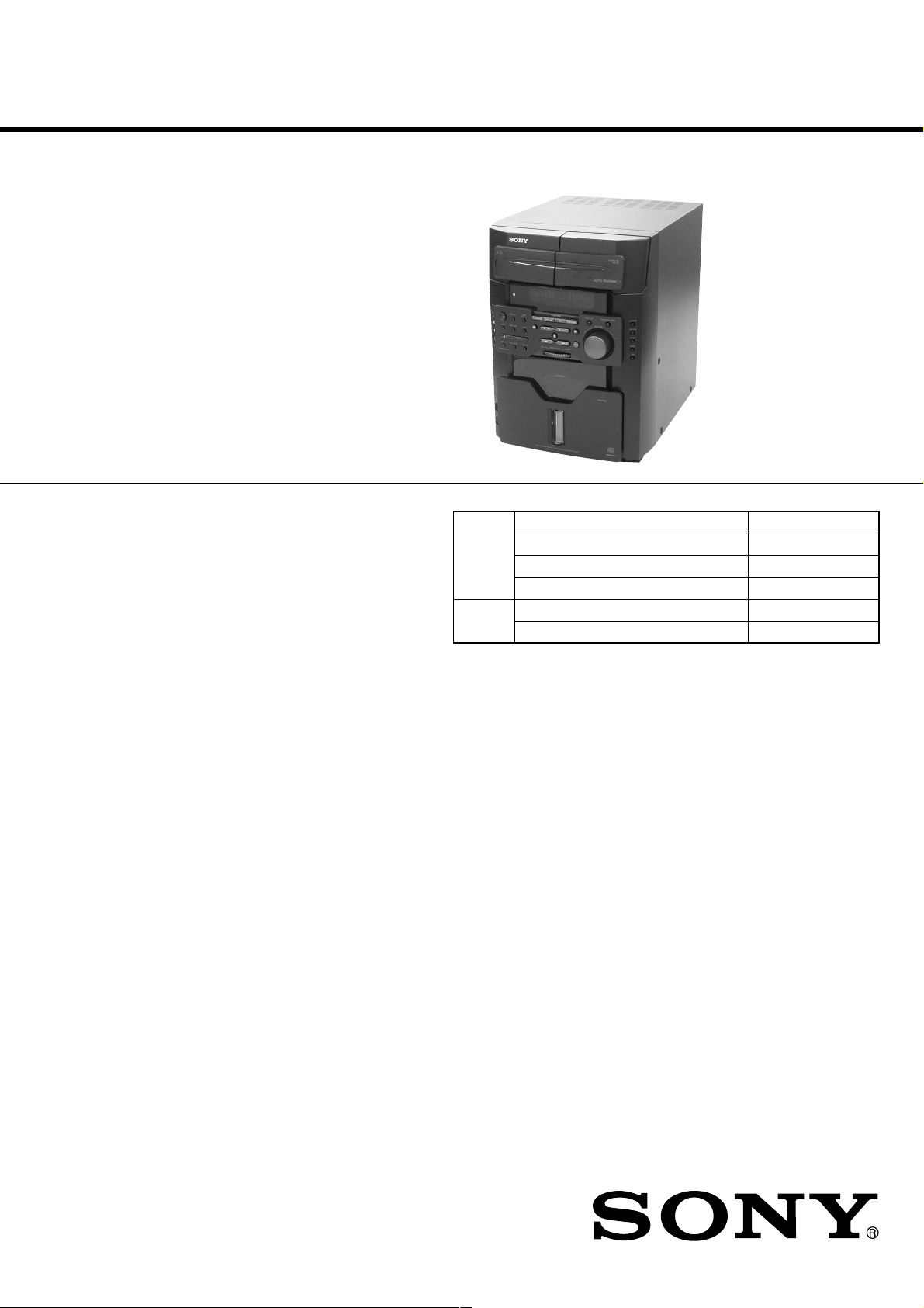
HCD-MG510AV
SERVICE MANUAL
Ver 1.0 2001.04
HCD-MG510AV are the Amplifier, CD player, Tape
Deck and Tuner section in MHC-MG510AV.
This stereo system is equipped with the Dolby* Pro Logic
Surround decoder.
* Manufactured under license from Dolby Laboratories.
Dolby, Pro Logic, and the double-D symbol ; are
trademarks of Dolby Laboratories. Confidential
unpublished works. '1992-1997 Dolby Laboratories.
All rights reserved.
CD
Section
TAPE
Section
US Model
Model Name Using Similar Mechanism HCD-MG310AV
CD Mechanism Type CDM64-K1BD44A
Base Unit Name BU-K1BD44A
Optical Pick-up Name KSM-213BFN
Model Name Using Similar Mechanism HCD-MG310AV
T ape Transport Mechanism Type CM8L6Z511A
Amplifier section Inputs
AUDIO POWER SPECIFICATIONS
POWER OUTPUT AND TOTAL
HARMONIC DISTORTION:
with 8 ohm loads both channels driven, from
120 – 10,000 Hz; rated 75 watts per channel
minimum RMS power, with no more than 10%
total harmonic distortion from 250 milliwatts to
rated output.
Front speaker:
Continuous RMS power output
Total harmonic distortion less than 0.09%
Center speaker:
Continuous RMS power output
Rear speaker:
Continuous RMS power output
Sub woofer:
Continuous RMS power output
75 + 75 watts
(8 ohms at 1 kHz,
10% THD)
(8 ohms at 1 kHz,
40 watts)
45 watts
(8 ohms at 1 kHz,
10% THD)
45 + 45 watts
(8 ohms at 1 kHz,
10% THD)
45 watts
(8 ohms at 100 Hz,
10% THD
VIDEO/MD IN (phono jacks):
5.1CH:
FRONT (phono jacks): voltage 450 mV,
REAR (phono jacks): voltage 450 mV,
CENTER (phono jack): voltage 450 mV,
SUB WOOFER (phono jack):
Outputs
PHONES (stereo phone jack):
FRONT SPEAKER: accepts impedance of 8 to
SURROUND SPEAKER REAR:
SURROUND SPEAKER CENTER:
SURROUND SPEAKER SUB WOOFER:
SPECIFICATIONS
voltage 250 mV/450 mV,
impedance 47 kilohms
impedance 47 kilohms
impedance 47 kilohms
impedance 47 kilohms
voltage 450 mV,
impedance 47 kilohms
accepts headphones of
8 ohms or more
16 ohms
accepts impedance of 8 to
16 ohms
accepts impedance of
8 ohms
accepts impedance of
8 ohms
COMPACT DISC DECK RECEIVER
CD player section
System Compact disc and digital
Laser Semiconductor laser
Frequency response 2 Hz – 20 kHz (±0.5 dB)
Wavelength 780 – 790 nm
Signal-to-noise ratio More than 90 dB
Dynamic range More than 90 dB
OPTICAL OUT (CD)
(Square optical connector jack, rear panel)
Wavelength 660 nm
Output Level –18 dBm
Tape player section
Recording system 4-track 2-channel stereo
Frequency response 40 – 13,000 Hz (±3 dB),
Wow and flutter ±0.15% W.Peak (IEC)
audio system
(λ = 780 nm)
Emission duration:
continuous
using Sony TYPE I
cassette
0.1% W.RMS (NAB)
±0.2% W.Peak (DIN)
– Continued on next page –
9-873-812-11 Sony Corporation
2001D0500-1 Home Audio Company
C 2001.4 Shinagawa Tec Service Manual Production Group

HCD-MG510AV
Tuner section
FM stereo, FM/AM superheterodyne tuner
FM tuner section
Tuning range 87.5 – 108.0 MHz
Antenna FM lead antenna
Antenna terminals 75 ohms unbalanced
Intermediate frequency 10.7 MHz
AM tuner section
Tuning range 530 – 1,710 kHz
Antenna AM loop antenna
Antenna terminals External antenna terminal
Intermediate frequency 450 kHz
TABLE OF CONTENTS
1. SERVICING NOTES ............................................... 4
2. GENERAL ................................................................... 5
3. DISASSEMBLY
3-1. Disassembly Flow ........................................................... 7
3-2. Upper Cover .................................................................... 8
3-3. Front Block Assy............................................................. 8
3-4. MAIN Board ................................................................... 9
3-5. Back Panel, DC FAN (M391)......................................... 9
3-6. MAIN AMP Board, POWER Board............................... 10
3-7. Middle (F) Assy, Bracket (Middle-R),
Power Bracket ................................................................. 10
3-8. CD Mechanism Deck (CDM64-K1BD44A) .................. 11
3-9. Base Unit (BU-K1BD44A)............................................. 11
3-10. BU Holder Assy .............................................................. 12
3-11. Motor Gear Assy (Sled) (M102), CD Board.................. 12
3-12. Op Base Assy (KSM-213BFN) ...................................... 13
3-13. Cassette Lid Assy (A)/(B)............................................... 13
3-14. Mech Deck (Tape)........................................................... 14
4. MECHANICAL ADJUSTMENTS....................... 15
General
(with the interval set at
10 kHz)
531 – 1,710 kHz
(with the interval set at
9 kHz)
Power requirements 120 V AC, 60 Hz
Power consumption 220 watts
Dimensions (w/h/d) incl. projecting parts and controls
Mass Approx. 11.5 kg
Design and specifications are subject to change
without notice.
Approx. 280 × 383 × 480
mm
5-8. Printed Wiring Board – CD Section – ............................ 25
5-9. Printed Wiring Boards
– CD MOTOR/SENSOR Section – ................................ 26
5-10. Schematic Diagram
– CD MOTOR/SENSOR Section – ................................ 27
5-11. Printed Wiring Board – TC Section –............................. 28
5-12. Schematic Diagram – TC Section – ............................... 29
5-13. Schematic Diagram – MAIN Section (1/4) –................. 30
5-14. Schematic Diagram – MAIN Section (2/4) –................. 31
5-15. Schematic Diagram – MAIN Section (3/4) –................. 32
5-16. Schematic Diagram – MAIN Section (4/4) –................. 33
5-17. Printed Wiring Board – MAIN Section –....................... 34
5-18. Printed Wiring Boards – MAIN AMP Section – ............ 36
5-19. Schematic Diagram – MAIN AMP Section – ................ 37
5-20. Printed Wiring Board – SUB AMP Section – ................ 38
5-21. Schematic Diagram – SUB AMP Section – ................... 38
5-22. Printed Wiring Boards – DISPLAY Section – ............... 40
5-23. Schematic Diagram – DISPLAY Section – .................... 41
5-24. Printed Wiring Board – CONTROL Section – ............... 42
5-25. Schematic Diagram – CONTROL Section –.................. 43
5-26. Printed Wiring Boards – POWER Section – .................. 44
5-27. Schematic Diagram – POWER Section – ...................... 45
5-28. IC Pin Function Description ........................................... 46
5. DIAGRAMS
5-1. Block Diagram – CD SERVO Section – ........................ 17
5-2. Block Diagram – TUNER/TAPE DECK Section – ...... 18
5-3. Block Diagram – SURROUND Section –...................... 19
5-4. Block Diagram – AMP Section – ................................... 20
5-5. Block Diagram
– DISPLAY/POWER SUPPLY Section – ...................... 21
5-6. Note for Printed Wiring Boards and
Schematic Diagrams ....................................................... 22
5-7. Schematic Diagram – CD Section – ............................... 24
6. EXPLODED VIEWS
6-1. General Section ............................................................... 52
6-2. Front Panel Section ......................................................... 53
6-3. Chassis Section ............................................................... 54
6-4. CD Mechanism Deck Section (CDM64-K1BD44A)..... 55
6-5. Base Unit Section (BU-K1BD44A) ............................... 56
7. ELECTRICAL PARTS LIST ............................... 57
2

HCD-MG510AV
r
Notes on chip component replacement
• Never reuse a disconnected chip component.
• Notice that the minus side of a tantalum capacitor may be dam-
aged by heat.
Flexible Circuit Board Repairing
• Keep the temperature of the soldering iron around 270 ˚C during repairing.
• Do not touch the soldering iron on the same conductor of the
circuit board (within 3 times).
• Be careful not to apply force on the conductor when soldering
or unsoldering.
SAFETY CHECK-OUT
After correcting the original service problem, perform the following safety check before releasing the set to the customer:
Check the antenna terminals, metal trim, “metallized” knobs,
screws, and all other exposed metal parts for AC leakage.
Check leakage as described below.
LEAKAGE TEST
The AC leakage from any exposed metal part to earth ground and
from all exposed metal parts to any exposed metal part having a
return to chassis, must not exceed 0.5 mA (500 microamperes.).
Leakage current can be measured by any one of three methods.
1. A commercial leakage tester , such as the Simpson 229 or RCA
WT -540A. Follo w the manufacturers’ instructions to use these
instruments.
2. A battery-operated AC milliammeter. The Data Precision 245
digital multimeter is suitable for this job.
3. Measuring the voltage drop across a resistor by means of a
VOM or battery-operated AC voltmeter. The “limit” indication is 0.75 V, so analog meters must have an accurate lowvoltage scale. The Simpson 250 and Sanwa SH-63Trd are examples of a passive VOM that is suitable. Nearly all battery
operated digital multimeters that have a 2 V AC range are
suitable. (See Fig. A)
CAUTION
Use of controls or adjustments or performance of procedures
other than those specified herein may result in hazardous radiation exposure.
NOTES ON HANDLING THE OPTICAL PICK-UP
BLOCK OR BASE UNIT
The laser diode in the optical pick-up block may suffer electrostatic break-down because of the potential difference generated
by the charged electrostatic load, etc. on clothing and the human
body.
During repair, pay attention to electrostatic break-down and also
use the procedure in the printed matter which is included in the
repair parts.
The flexible board is easily damaged and should be handled with
care.
NOTES ON LASER DIODE EMISSION CHECK
The laser beam on this model is concentrated so as to be focused
on the disc reflective surface by the objective lens in the optical
pick-up block. Therefore, when checking the laser diode emission, observe from more than 30 cm away from the objective lens.
To Exposed Metal
Parts on Set
AC
1.5 k
0.15 µF
Fig. A. Using an AC voltmeter to check AC leakage.
SAFETY-RELATED COMPONENT WARNING!!
COMPONENTS IDENTIFIED BY MARK 0 OR DOTTED
LINE WITH MARK 0 ON THE SCHEMATIC DIA GRAMS
AND IN THE PARTS LIST ARE CRITICAL TO SAFE
OPERATION. REPLACE THESE COMPONENTS WITH
SONY PARTS WHOSE PART NUMBERS APPEAR AS
SHOWN IN THIS MANUAL OR IN SUPPLEMENTS PUBLISHED BY SONY.
Ω
Earth Ground
voltmete
(0.75 V)
3
HCD-MG510AV
SECTION 1
SERVICING NOTES
CD-TEXT TEST DISC
This unit is able to display the test data (character information)
written in the CD on its fluorescent indicator tube.
The CD-TEXT TEST DISC (TGCS-313:4-989-366-01) is used
for checking the display.
To check, perform the following procedure.
Checking Method:
1. Press the I/1 button to turn the power on, set the disc to the
disc table with the “test disc” label facing up, and chuck the
disc.
2. Press the [CD] button to set CD function, and press the n N button
to playback the disc.
3. The following will be displayed on the liquid crystal display.
Display : 1KHZ/0DB/L R
4. Pressing the [-- ] or [ +] button, select the track. The text
data of each track will be displayed.
For details of the displayed contents for each track, refer to “Table
1: CD-TEXT TEST DISC TEXT Data Contents”.
Restrictions in CD-TEXT Display
In this unit, some special characters will not be displayed properly. These will be displayed as a space or a character resembling
it.
Table 1: CD-TEXT TEST DISC TEXT Data Contents
TRACK
No.
1 1kHz/0dB/L&R
2 20Hz/0dB/L&R
3 40Hz/0dB/L&R
4 100Hz/0dB/L&R
5 200Hz/0dB/L&R
6 500Hz/0dB/L&R
7 1kHz/0dB/L&R
8 5kHz/0dB/L&R
9 7kHz/0dB/L&R
10 10kHz/0dB/L&R
11 16kHz/0dB/L&R
12 18kHz/0dB/L&R
13 20kHz/0dB/L&R
14 1kHz/0dB/L&R
15 1kHz/–1dB/L&R
16 1kHz/–3dB/L&R
17 1kHz/–6dB/L&R
18 1kHz/–10dB/L&R
19 1kHz/–20dB/L&R
20 1kHz/–60dB/L&R
.>
(TRACKS No. 1 to 20:Normal Characters)
Displayed Contents
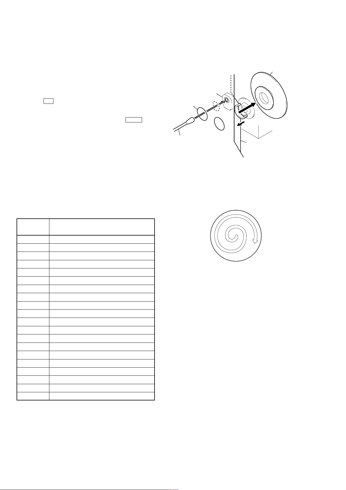
CLEANING OBJECTIVE LENS OF OPTICAL PICK-UP
• In cleaning the objective lens of optical pick-up, be sure the
following below.
2
Remove the
magnet assy.
optical pick-up
bracket (top 60) hole
A
3
Put a cotton bud into
the hole on the bracket
(top 60) and clean the
OP lens.
Note 1. In cleaning the lens, do not apply an excessive force.
As the optical pick-up is vulnerable, application of excessive
force could damage the lens holder.
Note 2. In cleaning, do not use a cleaner other than exclusive cleaning
liquid (KK-91 or isopropyl alcohol).
Note 3. Wipe the objective lens spirall y from center toward outside. (See
Figure A)
1
Open the torsion holder
(magnet) in direction of
arrow
A
.
(Figure A)
Note: Track No. 21 to 99 are not displayed.
4
Parts Identification
The items are arranged in alphabetical order.
Refer to the pages indicated in parentheses ( ) for details.
Main unit
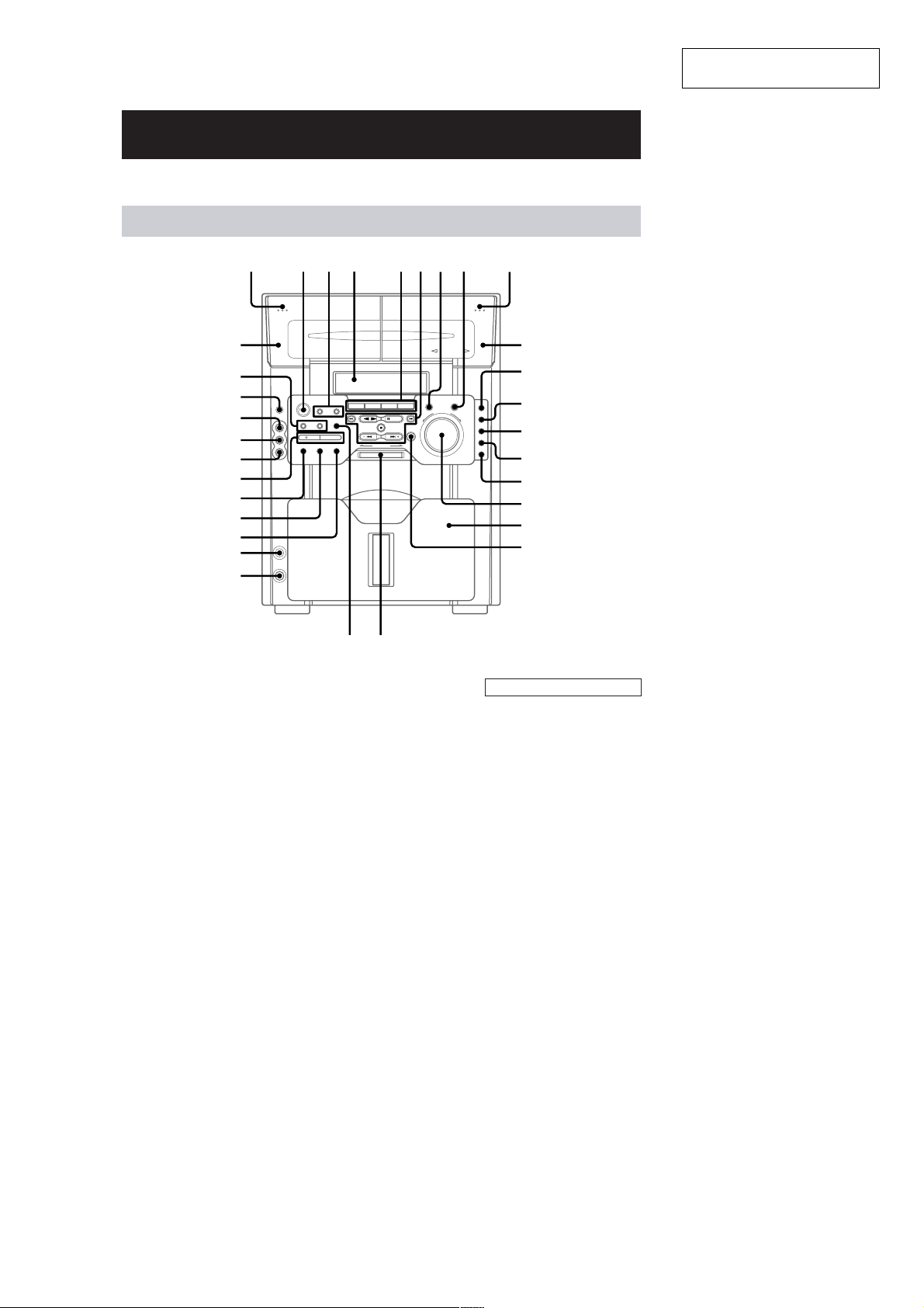
SECTION 2
GENERAL
HCD-MG510AV
This section is extracted from
instruction manual.
1
es
ea
e;
wl
wk
wj
wh
wg
wf
wd
ws
wa
5.1CH/VIDEO (MD) 5 (28 )
AUDIO IN L jack wk (29)
AUDIO IN R jack wj (29)
CD 5 (14, 21)
CD SYNCHRO wh (21, 22)
CLEAR w; (15, 19, 34)
Deck A es (20)
Deck B 0 (20)
DIRECTION ea (20)
DIS C ACCESS ql ( 12, 21)
Display window 4
DISPLAY wd (12, 17, 19, 34)
ENTER qk (11, 15, 18, 22, 26, 28)
FRONT qd (25)
GAME e; (26, 29)
KEYBOARD INPUT jack ws
(27)
LINK qg (25)
MENU ea (16, 18)
234
5
67 8 9
w; ql
PHONES jack wa
PLAY MODE wf (14, 22)
PRESET EQ 7 (24)
PRO LOGIC qs (11, 25)
PUSH OPEN (Front cover) qj
(12)
REAR qf (25)
REC PAUSE/START wh (21,22)
REPEAT wg (14)
STEREO/MONO wg (19)
SURROUND qa (25)
SURROUND MODE 8 (25)
TAPE A/B 5 (20)
TIMER SELECT 3 ( 23, 27)
TIMER SET 3 (11, 23, 26)
TUNER/BAND 5 (18)
VIDEO IN jack wl (29)
VOLUME control qh
0
qa
qs
qd
qf
qg
qh
qj
qk
BUTTON DESCRIPTIONS
Z (deck A) 1
=/1 (power) 2
m (rewind) 6
n N (play) 6
X PAUSE 6
M (fast forward) 6
x (stop) 6
– . (go back) 6
> + (go forward) 6
Z (deck B) 9
4
5

HCD-MG510AV
p
Remote Control
1234
wf
wd
ws
wa
w;
ql
qk
qj
qh
qg
5
6
7
8
9
0
qa
qs
qd
qf
5.1CH wa (30)
CD ql (14, 21)
CENTER +/– 5 (11)
DBFB qd (24)
DISPLAY 9 (12, 17, 19)
GAME 8 (26, 29)
GROOVE qf (24)
PLAY MODE 2 (14, 22)
PRESET EQ qk (24)
PRO LOGIC wf (11, 25)
REAR +/– 6 (11)
REPEAT 3 (14)
SCROLL qa (17)
SLEEP 1 (26)
SURROUND qh (25)
TAPE A/B w; (20)
TEST TONE ws (11)
TUNER/BAND 7 (18)
VIDEO (MD) wd (28)
VOL +/– qg
BUTTON DESCRIPTIONS
@/1 (power) 4
N (play) 0
X (pause) 0
x (stop) 0
. (go back) 0
m (rewind) 0
M (fast forward) 0
> (go forward) 0
TDISC/DISCt qs qj
Setting the time
1
Turn on the system.
2
Press TIMER SET.
When you set the clock for the first time, go
to step 5.
3
Press – . or > + repeatedly to
select “CLOCK SET”.
4
Press ENTER.
5
Press – . or > + repeatedly to set
the hour.
6
Press ENTER.
7
Press – . or > + repeatedly to set
the minute.
8
Press ENTER.
Tip
If you made a mistake or want to change the time,
start over from step 1.
Note
The clock settings are canceled when you disconnect
the
ower cord or if a power failure occurs.
6

• This set can be disassembled in the order shown below.
3-1. DISASSEMBLY FLOW
SET
3-2. UPPER COVER
(Page 8)
HCD-MG510AV
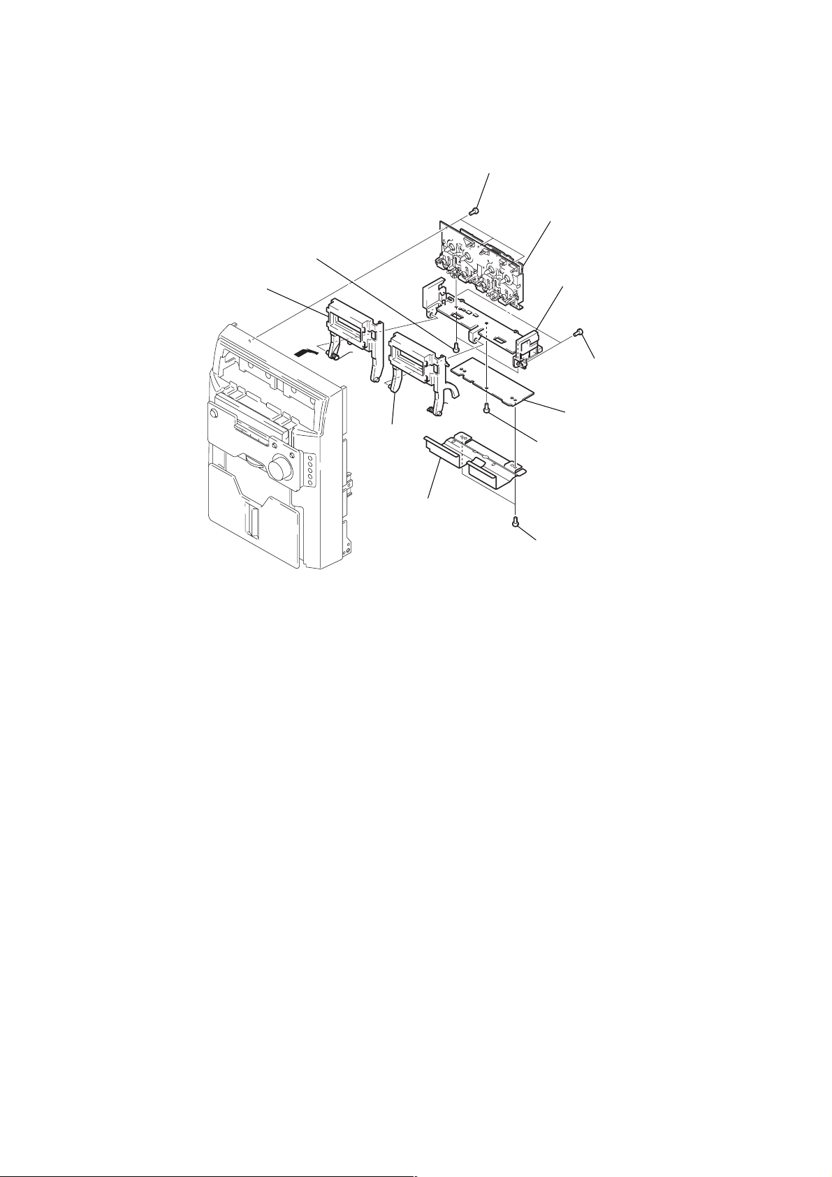
SECTION 3
DISASSEMBLY
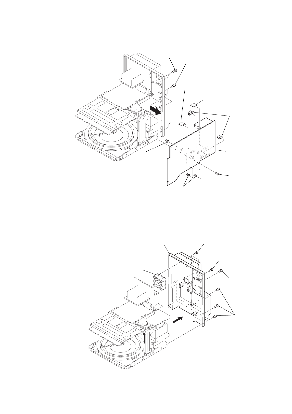
3-3. FRONT BLOCK ASSY
(Page 8)
3-4. MAIN BOARD
(Page 9)
3-5. BACK PANEL,
DC FAN (M391)
(Page 9)
3-6. MAIN AMP BOARD,
POWER BOARD
(Page 10)
3-7. MIDDLE (F) ASSY,
BRACKET (MIDDLE-R),
POWER BRACKET
(Page 10)
3-8. CD MECHANISM DECK
(CDM64-K1BD44A)
(Page 11)
3-13. CASSETTE LID ASSY (A)/(B)
(Page 13)
3-14. MECH DECK (TAPE)
(Page 14)
3-9. BASE UNIT
(BU-K1BD44A)
(Page 11)
3-10. BU HOLDER ASSY
(Page 12)
3-11. MOTOR GEAR ASSY
(SLED) (M102),
CD BOARD
(Page 12)
3-12. OP BASE ASSY
(KSM-213BFN)
(Page 13)
7
HCD-MG510AV
Note: Follow the disassembly procedure in the numerical order given.
3-2. UPPER COVER
3
upper cover
1
three screws
(BVTP3
×
8)
2
five screws
(BVTP3
2
two screws
(BVTP3
1
three screws
(BVTP3
×
8)
×
8)
×
8)
3-3. FRONT BLOCK ASSY
2
6
front block assy
4
screw (KTP3 × 8)
1
wire (flat type) (11 core)
(CN312)
1
wire (flat type) (17 core)
(CN301)
three connectors
(CN310, 503, 803)
5
two bosses
1
wire (flat type) (10 core)
(CN311)
5
two bosses
4
screw (KTP3 × 8)
3
three screws
(BVTP3 × 8)
8
3-4. MAIN BOARD
s
s
2
connector
(CN313)
3
two screws
(BVTP3 × 8)
3
three screws
(BVTP3 × 8)
1
wire (flat type) (18 core)
(CN309)
1
wire (flat type) (21 core)
(CN303)
HCD-MG510AV
2
two connector
(CN304, 903)
5
MAIN board
3-5. BACK PANEL, DC FAN (M391)
4
DC fan (M391)
5
back panel
2
two connectors
(CN305, 317)
2
3
four screws
(BVTP3 × 10)
4
1
two screws
(BVTP3 × 10)
1
screw
(BVTP3 × 8)
two screws
(BVTP3
×
eleven screw
1
(BVTP3 × 10)
10)
9
HCD-MG510AV
)
3-6. MAIN AMP BOARD, POWER BOARD
1
connector
(CN502)
4
three screws
5
center bracket
(BVTP3
×
8)
2
two screws
(BVTP3
×
8)
2
four screws
(BVTP3
×
8)
3
MAIN AMP board
7
POWER board
6
two screws
(BVTP4
×
8
3-7. MIDDLE (F) ASSY, BRACKET (MIDDLE-R), POWER BRACKET
6
bracket (middle-R)
4
two screws
2
screw (BVTP3 × 8)
1
screw (BVTP3 × 8)
(BVTP3
×
8)
6
two screws
(BVTP4
5
two screws
(BVTP3
×
8)
×
8)
8
three screws
(BVTP3
9
two screws
(BVTP3
×
8)
×
8)
10
3
middle (F) assy
2
screw
(BVTP3
×
7
8)
screw
(BVTP3
0
×
8)
power bracket
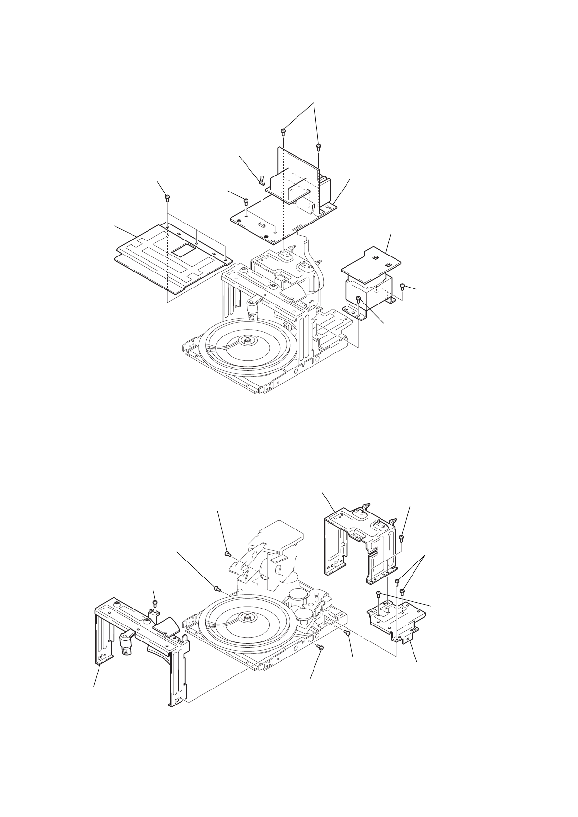
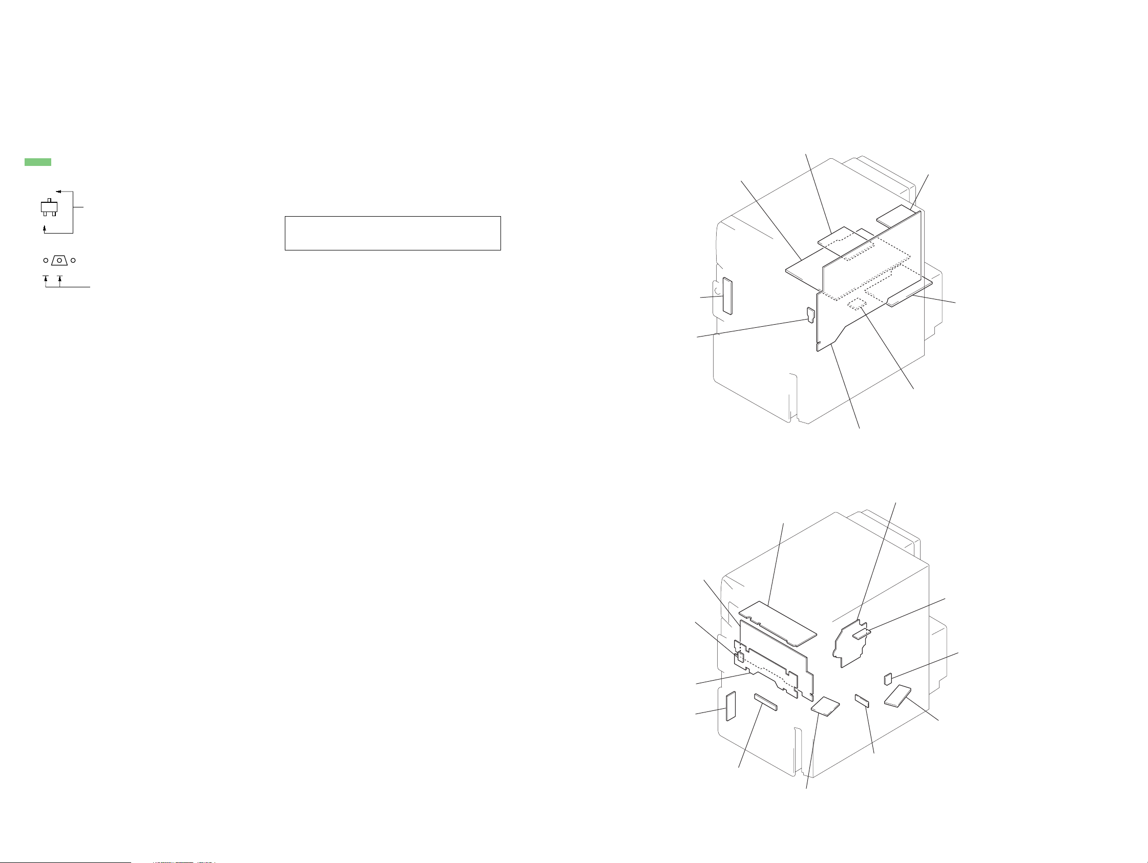
3-8. CD MECHANISM DECK
)
(CDM64-K1BD44A)
1
screw (2.6 × 8)
2
table (60)
5
CD mechanism deck
(CDM64-K1BD44A)
HCD-MG510AV
4
two screws
(BVTP3
×
8
3-9. BASE UNIT
(BU-K1BD44A)
1
three screws
(BVTP3
×
8)
lower chassis
2
bracket (top 60)
4
four screws
(BVTP3
3
screw
(PSW3
×
6)
4
×
8)
four screws
(BVTP3
×
3
base unit
(BU-K1BD44A)
8)
11
HCD-MG510AV
)
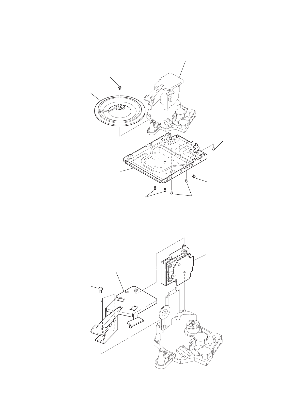
3-10. BU HOLDER ASSY
1
tension spring (F1)
2
tension spring (F-2)
3
two screws
(PTP2.6
×
8
4
BU holder assy
3-11. MOTOR GEAR ASSY (SLED) (M102), CD BOARD
7
2
two screws
(P2
gear
6
claw
×
3)
8
3
two screws
(PTP2.6
claw
9
gear cover
0
×
8)
8
gear
two claws
12
qd
1
Remove two
solders.
CD board
4
qa
Remove two solders.
5
parallel (FFC) (16 core) wire
(CN102)
qs
motor gear assy (SLED)
(M102)
3
screw (P2 × 5)

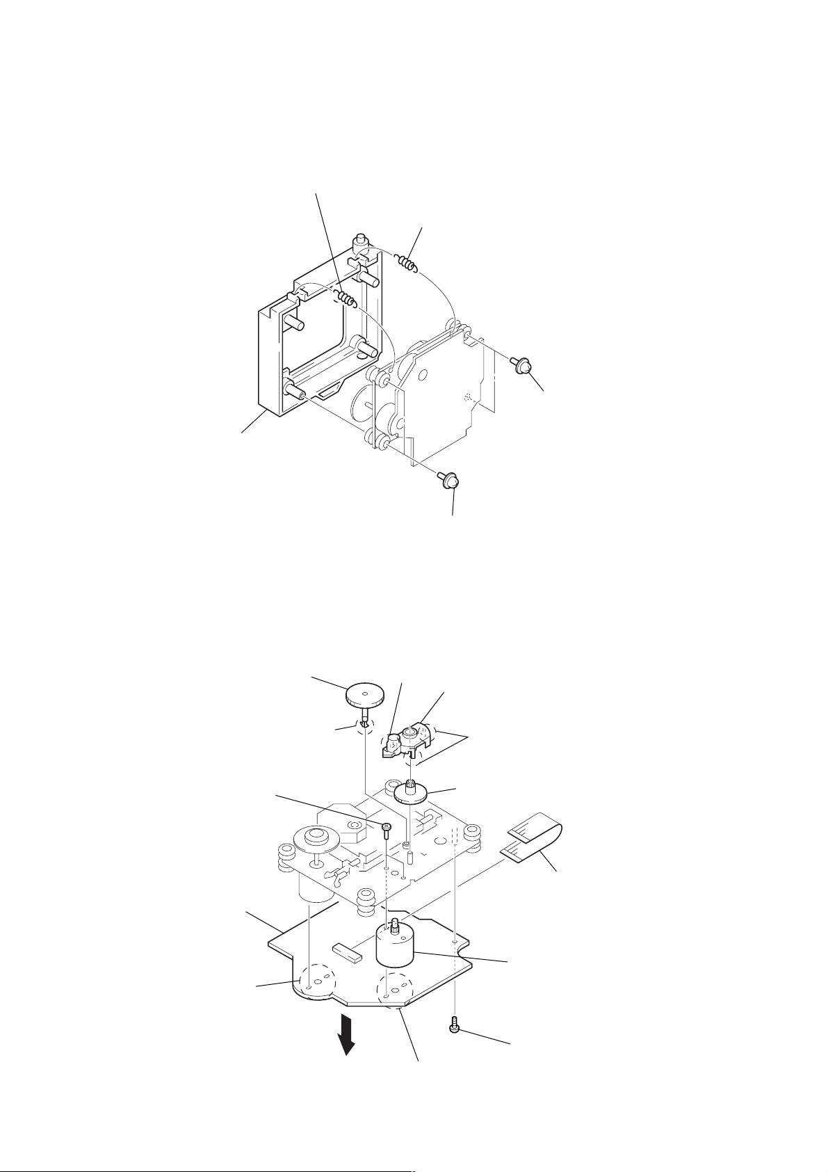
3-12. OP BASE ASSY
n
d
(KSM-213BFN)
3
Remove the optical pick-up
(KSM-213BFN) in the directio
of arrow B.
B
HCD-MG510AV
2
sled shaft
3-13. CASSETTE LID ASSY (A) / (B)
1
Open the cassette lid
assy (A)/(B).
A
1
Slide the lever
in the direction of arrow
A
.
2
two claws
3
cassette lid
assy (A)
4
two claws
5
cassette li
assy (B)
13
HCD-MG510AV
)
3-14. MECH DECK (TAPE)
4
cassette holder assy (A)
0
two screws
(BVTP2.6)
1
three screws
(BVTP3
×
10)
qs
mech deck (tape)
qa
MD bracket
3
5
cassette
holder
assy (B)
7
shield plate (MD)
2
9
TC board
8
screw (BVTP2.6)
6
two screws
(BVTP2.6)
two screws
(BVTP3 × 10
14

SECTION 4
MECHANICAL ADJUSTMENTS
HCD-MG510AV
• TAPE MECHANISM DECK SECTION
Precaution
1. Clean the following parts with a denatured alcohol-moistened
swab:
record/playback heads pinch rollers
erase head rubber belts
capstan idlers
2. Demagnetize the record/playback head with a head demagnetizer.
3. Do not use a magnetized screwdriver for the adjustments.
4. After the adjustments, apply suitable locking compound to the
parts adjusted.
5. The adjustments should be performed with the rated power
supply voltage unless otherwise noted.
Torque Measurement
Mode
FWD
FWD
back tension
REV
REV
back tension
FF/REW
FWD tension
REV tension
Torque meter
CQ-102C
CQ-102C
CQ-102RC
CQ-102RC
CQ-201B
CQ-403A
CQ-403R
Meter reading
2.94 mN • m to 7.84 mN • m
31 to 71 g • cm
(0.43 – 0.98 oz • inch)
0.14 mN • m to 0.59 mN • m
2 to 6 g • cm
(0.02 – 0.08 oz • inch)
2.94 mN • m to 7.84 mN • m
31 to 71 g • cm
(0.43 – 0.98 oz • inch)
0.14 mN • m to 0.59 mN • m
2 to 6 g • cm
(0.02 – 0.08 oz • inch)
6.86 mN • m to 17.64 mN • m
71 to 143 g • cm
(0.98 – 1.99 oz • inch)
more than 0.98 N • m
100 g or more
(3.53 oz or more)
more than 0.98 N • m
100 g or more
(3.53 oz or more)
15

HCD-MG510AV
MEMO
16
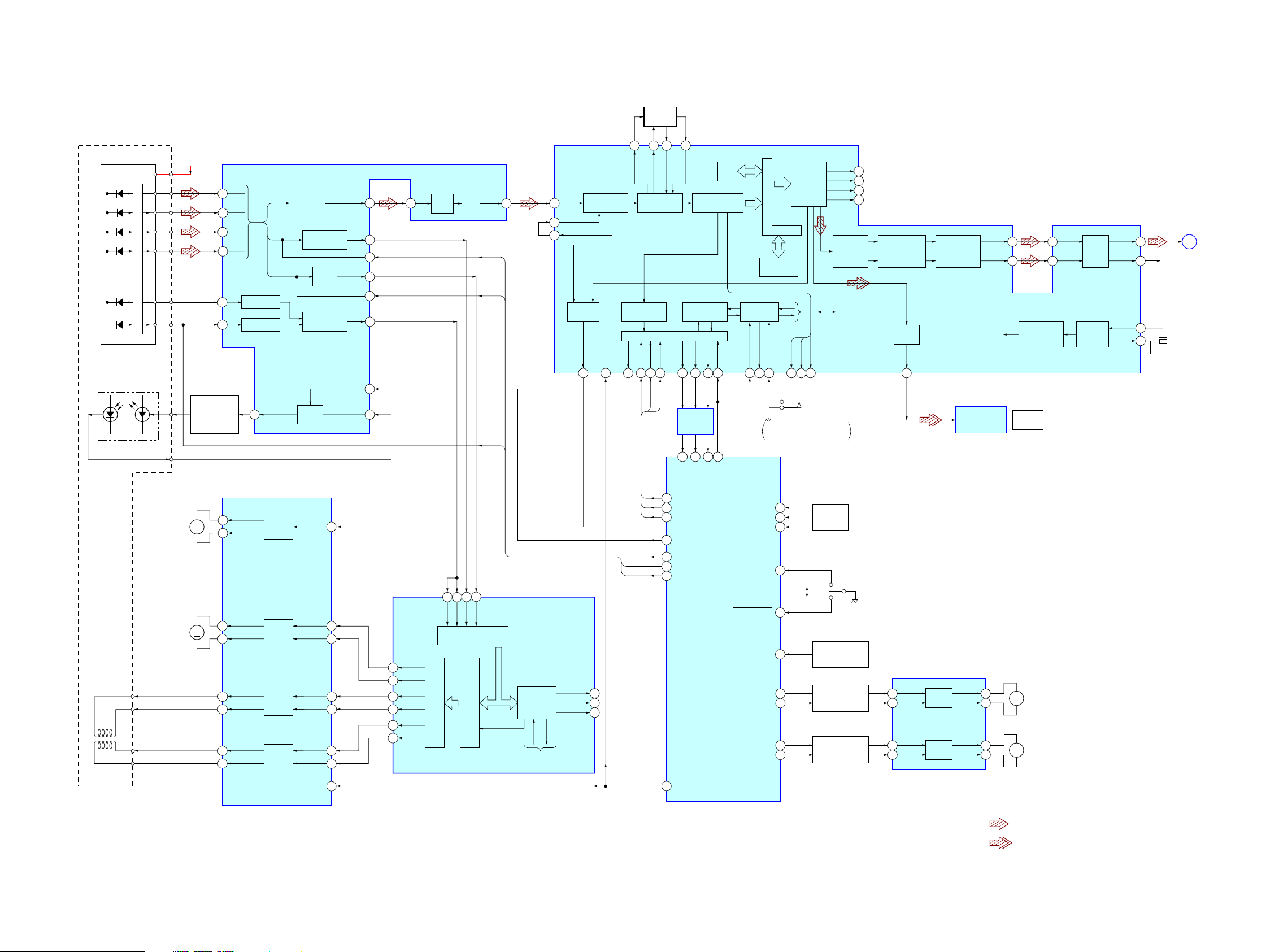
SECTION 5
DIAGRAMS
5-1. BLOCK DIAGRAM – CD SERVO Section –
HCD-MG510AV
DETECTOR
A
B
C
D
F
E
OPTICAL PICK-UP
BLOCK
(KSM-213BFN)
LASER DIODE
PD
I-V AMP
LD
CD +5V
6
7
8
9
11
10
AUTOMATIC
POWER
CONTROL
Q101
A
B
C
D
F
E
F I-V AMP
E I-V AMP
LD
1
FOCUS/TRACKING ERROR AMP
RF
SUMMING
AMP
FOCUS
ERROR AMP
RF DC
AMP
TRACKING
ERROR AMP
APC LD
AMP
AC
SUM
RFDCO
RFDCI
SW
RF AMP,
IC103
FE
FEI
TE
PD
FILTER
53
54 56
FILO
EQ
IN
4
16
17
28
29
18
12
2
RFAC
3
VCA
RFAC
EQ
15
PWM1
PWM3
PWM2
RFAC
51
49
48
ASYMMETRY
CORRECTION
ASYI
ASYO
DIGITAL
CLV
MDP
XRST
26 7 8
3
SUBCODE
PROCESSOR
XLON
DATA
CLOK
14 5
PCO
CLTV
DIGITAL
PLL
CPU INTERFACE
XLAT
SENS
6
84 19
55
DIGITAL SIGNAL PROCESSOR,
DIGITAL FILTER, D/A CONVERTER
FILI
LEVEL
SHIFT
IC803
EFM
DEMODULATOR
SERVO AUTO
SEQUENCER
SQSO
SCOR
20
1 2
32 33
16K
RAM
SQCK
IC101 (1/2)
CORRECTOR
SERVO
INTERFACE
SCLK
COUT
9 21
D/A
INTERFACE
INTERNAL BUS
ERROR
SSTP
EMPH
WFCK
GFS
64 15
27
ON :
18
S101
(LIMIT)
When the optical pick-up
is inner position
PCMD
62
BCK
63
LRCK
61
C2PO
19
SERIAL
IN
INTERFACE
TO MIRR/DFCT/
FOK DETECTOR
DIGITAL
FILTER,
NOISE SHAPER
DIGITAL
OUT
DOUT
60
PWM
&
INTEGRATOR
TRANSCEIVER
OPTICAL
IC361
AOUT1
AOUT2
70
77
OPTICAL
OUT (CD)
71
76
CLOCK
GENERATOR
AIN1
AIN2
BUFFER
TIMING
LOGIC
LOUT1
LOUT2
XTAI
XTAO
CD
L-CH
72
75
R-CH
66
67
A
X101
16.9344MHz
(Page 19)
2-AXIS
DEVICE
(TRACKING)
(FOCUS)
M101
(SPINDLE)
M102
(SLED)
FOCUS/TRACKING COIL DRIVE,
SPINDLE/SLED MOTOR DRIVE
IC102
CH4OUTF
15
M
M
16
17
18
11
12
13
14
CH4OUTR
CH3OUTF
CH3OUTR
CH2OUTR
CH2OUTF
CH1OUTR
CH1OUTF
MOTOR
DRIVE
MOTOR
DRIVE
COIL
DRIVE
COIL
DRIVE
CH4SIN
CH3FIN
CH3RIN
CH2RIN
CH2FIN
CH1RIN
CH1FIN
MUTE
25
PWM1
PWM2
PWM3
43
39
40
41
FE
TE
SE
24
23
SFDR
28
SRDR
29
6
5
3
2
20
TFDR
30
TRDR
31
FFDR
32
FRDR
33
PWM GENERATOR
FOCUS/TRACKING/SLED
RFDC
A/D
CONVERTER
SERVO DSP
FOCUS/TRACKING/SLED
DIGITAL SERVO
PROCESSOR
IC101 (2/2)
MIRR/DFCT/
FOK
DETECTOR
TO SERVO INTERFACE
FOK
MIRR
DFCT
24
22
23
85
87
86
88
22
24
26
83
C-SENS
C-DATA
C-CLK
C-LATCH
LD ON
PWM1
PWM2
PWM3
C-XRST
C-SQCK
C-SCOR
C-SQSO
LOAD IN SW 6
LOAD OUT SW 7
SYSTEM CONTROLLER
IC801 (1/5)
LOAD NEG 3
LOAD POS
TABLE POS 5
TABLE NEG
T-SENS1
T-SENS2
T-SENS3
D-SENS 92
93
18
91
2
100
LOAD IN
LOAD OUT
TABLE
SENSOR
IC11 – 13
S842
(LOAD)
DISC IN
DETECT SENSOR
D841, Q841
LOADING
MOTOR CONTROL
Q881 – 884
TABLE
MOTOR CONTROL
Q885 – 888
2
3
17
16
LOADING/TABLE
MOTOR DRIVE
FN1
RN1
FIN2
RIN2
IC881
MOTOR
DRIVE
MOTOR
DRIVE
OUT1 +
OUT1 –
OUT2 +
OUT2 –
8
9
11
10
M
M
M51
(LOADING)
M52
(TABLE)
• R-ch is omitted due to same as L-ch.
• SIGNAL PATH
: CD PLAY (ANALOG)
: CD PLAY (DIGITAL OUT)
1717

HCD-MG510AV
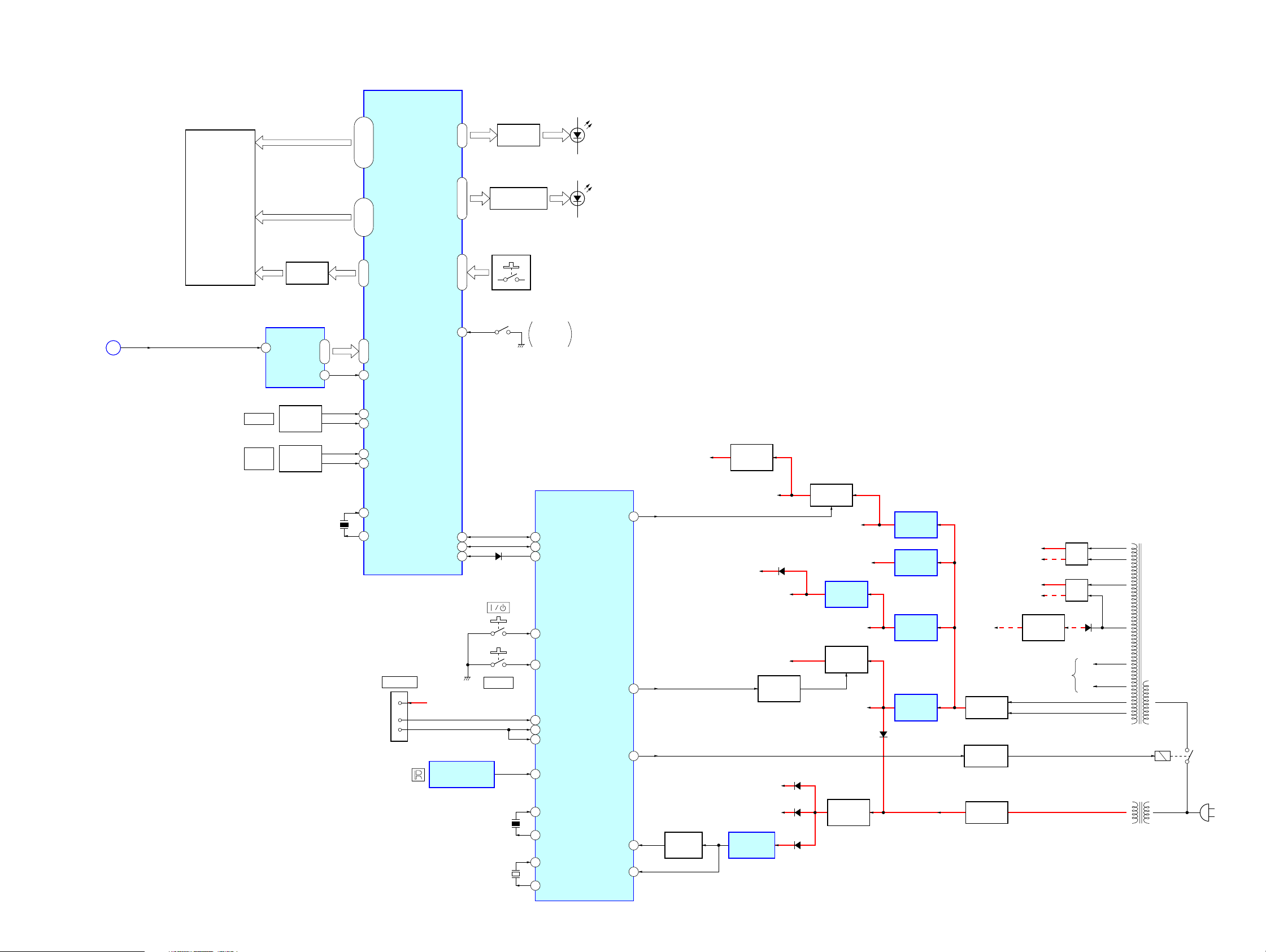
5-2. BLOCK DIAGRAM – TUNER/TAPE DECK Section –
FM 75Ω
HP101
(PLAY)
AM
L-CH
R-CH
L-CH
R-CH
R-CH
R-CH
FM ANT
ANT GND
AM ANT
ANT GND
TUNER PACK
R-CH R-CH
L-CH
R-CH
TU-CLK
TU-CE
TUNED
DI
DO
REC/PB SWITCHING
13
TUNER
L-CH
R-CH
DI
DO
CLK
CE
TUNED
5.1CH
INPUT SELECT
SWITCH
PB AMP
IC401 (1/2)
A IN-L
24
B IN-L
23
IC402
A/B SW
19
R-CH
PB
AMP
R-CH
PB-L
20
MIX
OUT
6
+
AMS DET
Q404, 405
MUTING
Q102
MUTING
Q101
R-CHR-CH
IC306
1 2
4 3
5 13
TAPE
L-CH
R-CHR-CH
B
C
D
(Page 19)
(Page 19)
(Page 19)
HRPE101
(REC/PLAY/ERASE)
R-CH
M1
(CAPSTAN)
BIAS OSC
T401
SENSOR B+
MM
T403
2
BIAS OSC
C429, R429
Q401
MOTOR DRIVE
BIAS
TRAP
REC BIAS
Q402, 403
CAPSTAN
Q381, 382
SWITCH
MOTOR
+12V
4
AU +9V
58 MO-ON
54
53
PB/REC
PB-A/B
(DECK A PLAY)
61
A-PLAY
16
67
AMS
B-PLAY
56
(DECK B PLAY)
REC
OUT-L
REC AMP
IC401 (2/2)
REC
AMP
(DECK A HALF)
TAPE MECHANISM
DECK BLOCK
(1/2)
REC
IN-L
66
14
R-CH
A-HALF
MUTING
Q112
50
REC-MUTE
(DECK B HALF)
(DECK B REC)
68
PB-MUTE
B-HALF
90
69
TAPE
(DECK A REC)
70
DVD
SYSTEM CONTROLLER
TAPE MECHANISM
DECK BLOCK
(2/2)
ROTATION
DETECT SENSOR
(DECK A)
97
A-SHUT
IC801 (2/5)
ROTATION
DETECT SENSOR
(DECK B)
89
B-SHUT
TRIGGER PLUNGER
(DECK A)
TRIGGER
PLUNGER DRIVE
(DECK A)
Q383, 384
59
A-TRIG
TRIGGER PLUNGER
(DECK B)
TRIGGER
PLUNGER DRIVE
(DECK B)
Q385, 386
• R-ch is omitted due to same as L-ch.
• SIGNAL PATH
: TUNER
: TAPE PLAY (DECK A)
: TAPE PLAY (DECK B)
60
B-TRIG
DI
DO
CLK
78
80
79
TU-DI
TU-DO
TU-CLK
: REC
: 5.1CH INPUT
CE
77
TUNED
76
TU-CE
TU-TUNED
REC
L-CH
E
(Page 19)
1818

5-3. BLOCK DIAGRAM – SURROUND Section –
HCD-MG510AV
5.1CH
INPUT
VIDEO IN
AUDIO
FRONT
REAR
CENTER
SUPER
WOOFER
(Page 21)
(Page 18)
(Page 17)
(Page 18)
(Page 18)
L
R
L
R
VIDEO
(Page 18)
L
R
L
R
J302
J701
J301
F
E
A
B
D
C
SPE ANA
REC
L-CH
CD
L-CH
TUNER
L-CH
TAPE
L-CH
R-CH
R-CH
5.1CH
R-CH
R-CH
3
5
7
1
9
J304
VIDEO OUT
FRONT
REAR
CENTER
WOOFER
B1
C1
D1
A1
E1
INPUT SELECT
IC302 (1/2)
INPUT SELECT
LOGIC
DATA
DATA
+
R-CH
CLK
1514
CLK
DATA
CLK
LINE
OUT
LOW-PASS
FILTER
IC304 (1/2)
DOLBY PRO LOGIC
SURROUND PROCESSOR
IC301
AUTO-BALANCE
L–R
SW
OUT
INPUT
DS2L
OUT
WOOFER
FRONT
32
CENTER
REAR
79
80
72
74
76
77
SWIN
VRSWIN
LIN
LTIN
CIN
SLIN
L+R
R-CH
2
SWVOL
IN
SELECTOR
COMMAND
REQ
TRIMMER,
VOLUME
ADAPTIVE
MATRIX
S
DIN
R-CH
L
R
C
10KBIT S-RAM
LOGIC
CIRCUIT
PSEUDO
STEREO
PS
RIN
CENTER
MODE
CONTROL
PS
LIN
DELAY
VOLUME
1615
NOISE
SEQUENCER
26 27
CPU
INTERFACE
DATA
SCK
22 23 24 8 7 6
27 28 25
R-CH
DVOL
OUT
OUT
SL
OUT
SWVOL OUT
+
MODIFIED
BNR
BNR
IN
4240
C
45
1011
CVOL
IN
SLVOL
IN
TRIMMER,
VOLUME
TRIMMER,
VOLUME
R-CH
SLVOL OUT
LOUT
CVOL OUT
17
1
3
9
BAND-PASS
FILTER
IC305
ELECTRICAL VOLUME
VOL1
29
IC302 (2/2)
SOUND
CONTROL
AMP
IC304 (2/2)
OUT1
20
• R-ch is omitted due to same as L-ch.
R-CH
+
SW
(Page 20)
Z
FRONT
L-CH
CENTER
REAR
L-CH
G
H
J
(Page 20)
(Page 20)
(Page 20)
• SIGNAL PATH
51 V-DATA
52 V-CLK
SYSTEM CONTROLLER
IC801 (3/5)
PL-CLK
PL-DATA
PL-RQ
: TUNER
: CD PLAY
: TAPE PLAY
: REC
: VIDEO IN (AUDIO)
: GAME IN (AUDIO)
: GAME IN (VIDEO)
: 5.1CH INPUT
1919

HCD-MG510AV
5-4. BLOCK DIAGRAM – AMP Section –
J503
PHONE
(Page 19)
(Page 19)
(Page 19)
(Page 19)
G
H
Z
J
FRONT
L-CH
REAR
L-CH
CENTER
SW
D395, 399
D389
DBFB AMP
IC303
DBFB
SWITCH
Q141
DBFB LEVEL
CONTROL
Q142
R-CH
REAR OUTPUT
SELECT SWITCH
IC307
6 12
R-CH R-CH
R-CH
1011
98
R-CH
STK MUTE
STK MUTE
R-CH
R-MUTE
C-MUTE
SW-MUTE
Q524
MUTING
Q517, 518
MUTING
CONTROL
Q522
MUTING
Q602, 603
MUTING
CONTROL
Q341, 342
MUTING
Q601
MUTING
CONTROL
Q343, 344
MUTING
Q232
MUTING
CONTROL
Q333, 334
POWER AMP
IC501
MUTING
Q501
MUTING
CONTROL
Q502, 516
POWER AMP
IC602
POWER AMP
IC601
AU +9V
POWER ON
MUTING
Q521
TH501
D513
TERMINAL
DETECT
Q511, 512
PROTECT
DETECT
Q514
+
PROTECTOR
Q505, 508
OVER LOAD
DETECT
Q604, 605
OVER LOAD
DETECT
Q608
OVER LOAD
DETECT
Q607
D501
OVER LOAD
DETECT
Q506, 507
DC DETECT
Q513, 515
+ + +
RY501
MUTING
Q519, 520
MUTING
+
CONTROL
Q523
RELAY DRIVE
Q504, 510
F-RELAY
+
D503
++
RY502
+
+ +
RY503
+
++
HP CHK
FAN MOTOR
DRIVE
Q391, 392
J501 (1/2)
+
–
+
–
M391
(FAN)
M
J501 (2/2)
+
–
+
–
+
–
+
–
L
FRONT SPEAKER
IMPEDANCE
USE 8Ω
R
L
REAR
IMPEDANCE
USE 8Ω
R
CENTER
IMPEDANCE
USE 8Ω
SUPER WOOFER
IMPEDANCE
USE 8Ω
SURROUND
SPEAKER
47
DBFB-ON
48
DBFB-H/L
35
REAR
34
FRONT
STK-MUTE
65
44
STK-MUTE
A-MUTE
R-MUTE
23
A-MUTE
C-MUTE
21
38
C-MUTE
R-MUTE
SW-MUTE
S/W MUTE
SYSTEM CONTROLLER
IC801 (4/5)
RELAY DRIVE
Q503, 509
HP CHK
F-RELAY
40
R-RELAY
55
F-RELAY
45
HP-CHK
• R-ch is omitted due to same as L-ch.
• SIGNAL PATH
: TUNER
2020
5-5. BLOCK DIAGRAM – DISPLAY/POWER SUPPLY Section –
22 – 12
S1 – S34
47 – 43,41 – 24,
LED3 – LED7
HCD-MG510AV
GRID DRIVE
LED DRIVE
Q721 – 723
89 – 93
Q713 – 717
D703 – 707
(Page 19)
X
F
SPE ANA
FL701
FLUORESCENT
INDICATOR TUBE
VOLUME
DISC
ACCESS
BAND-PASS
4 LINE IN
GRID DRIVE
GRID DRIVE
Q721 – 723
Q721 – 723
FILTER
IC703
ROTARY
ENCODER
RV701
ROTARY
ENCODER
RV702
F1 – F4
13L+R
X701
4MHz
IC801 (5/5)
D708, 736,
D781, 782, 791
CD +3V
81CD POWER
71FM-ON
42POWER STBY
12RESET
82AC CUT
RESET
SWITCH
Q801
+3.3V
REGULATOR
Q102
CD +5V
FL +3.3V
REGULATOR
BU +5V
U-COM +5V
RESET SIGNAL
GENERATOR
IC802
D701, 702
B+ 5V
FM +7V
CONTROL
Q350, 351
D802
D803
D806
B+ SWITCH
Q361, 362
COM +5V
REGULATOR
IC905
MOTOR +12V
REGULATOR
REGULATOR
Q802, 803
+5V
+7V
Q352
+5.6V
CD +8V
AU +9V
D866
+5V
REGULATOR
IC904
+8V
REGULATOR
IC903
+12V
REGULATOR
IC902
+9V
REGULATOR
IC901
VP – 33V
RECT
D961 – 964
RELAY DRIVE
Q901
RECT
D911 – 914
R AMP B+
R AMP B–
F AMP B+
F AMP B–
– 33V
REGULATOR
Q397
TO FLUORESCENT
INDICATOR TUBE
FL701
RECT
D507
RECT
D511
D901
RECT
VF1
VF2
T901
POWER
TRANSFORMER
(MAIN)
T902
POWER
TRANSFORMER
(SUB)
RY901
(AC IN)
LED DRIVE
86, 87, 94, 95
80 – 78, 76
S700
S770
DISPLAY
X802
16MHz
X801
32.768kHz
Q702 – 705, 718
OPEN/CLOSE
30 IIC DATA
29 IIC CLK
43 FL-RESET
74 POWER KEY
73 DISPLAY KEY
36 KB-SDA
20 KB-SCL
37 KB-CTRL
15 XIN
13 XOUT
10 SUBXIN
11 SUBXOUT
S701, 741 – 745,
S750 – 757, 760 – 767,
S771 – 777
S791
CD LID
DETECT
SYSTEM CONTROLLER
4 RMC
LED8, LED9
LED0, LED1,
3, 5 – 10
G8 – G13
99, 100, 2,
G2, G3, G5, G6,
98, 1, 4
G1, G4, G7
DISPLAY CONTROLLER
IC701
17 – 14
75 – 72
BPF1 – BPF4
71 L+R
66 VOL A
67 VOL B
64 JOG A
65 JOG B
82 X0
83 X1
SDA
SCL
J801
KEYBOARD
4
1
5
KEY0 – KEY3
59DOOR SW
60SDA
61SCL
77RSTX
B+ 5V+5V
REMOTE CONTORL
RECEIVER
IC702
2121
HCD-MG510AV
d
5-6. NOTE FOR PRINTED WIRING BOARDS AND SCHEMATIC DIAGRAMS
(In addition to this, the necessary note is printed in each block)
Note on Printed Wiring Boards:
• X : parts extracted from the component side.
• Y : parts extracted from the conductor side.
• W : indicates side identified with part number.
f
•
• : Pattern from the side which enables seeing.
• Indication of transistor.
: internal component.
C
Q
B
E
B
These are omitted.
Q
CE
These are omitted.
Note on Schematic Diagram:
• All capacitors are in µF unless otherwise noted. pF: µµF
50 WV or less are not indicated except for electrolytics
and tantalums.
• All resistors are in Ω and 1/
specified.
f
•
• 2 : nonflammable resistor.
• 5 : fusible resistor .
• C : panel designation.
Note: The components identified by mark 0 or dotted line
• A : B+ Line.
• B : B– Line.
• Voltages are taken with a VOM (Input impedance 10 MΩ).
• Waveforms are taken with a oscilloscope.
• Circled numbers refer to waveforms.
• Signal path.
: internal component.
with mark 0 are critical for safety.
Replace only with part number specified.
Voltage var iations may be noted due to normal production tolerances.
Voltage var iations may be noted due to normal production tolerances.
F : TUNER
J : CD PLAY (ANALOG)
c : CD PLAY (DIGITAL OUT)
E : TAPE PLAY (DECK A)
d : TAPE PLAY (DECK B)
G : REC
q : VIDEO IN (AUDIO)
j : GAME IN (AUDIO)
k : GAME IN (VIDEO)
f : 5.1CH INPUT
4
W or less unless otherwise
• Circuit Boards Location
GAME LINK board
CD LED board
MAIN AMP board
SUB AMP board
FM/AM TUNER PACK
POWER board
FUSE board
MAIN board
CD board
TC board
DISPLAY board
D SENSOR (OUT) boar
RMC board
LOAD SW board
CONTROL board
H/P board
L. T MOTOR board
D SENSOR (IN) board
DOOR LED board
T SENSOR board
2222
 Loading...