

Sony HCD-LX5, HCD-LX6, HCD-LX30, HCD-LX50 Service manual
HCD-LX5/LX6/LX30/LX50
SERVICE MANUAL
HCD-LX5/LX6/LX30/LX50 are the
Amplifier, CD player, Tape Deck and Tuner
section in LBT-LX5/LX6/LX30/LX50.
Dolby noise reduction manufactured under license
from Dolby Laboratories Licensing Corporation.
“DOLBY” and the double-D symbol ; are trademarks of Dolby Laboratories Licensing Corporation.
Photo: HCD-LX50
CD
Section
TAPE
Section
US Model
HCD-LX30/LX50
Canadian Model
HCD-LX50
AEP Model
UK Model
HCD-LX5
E Model
Australian Model
HCD-LX6
Model Name Using Similar Mechanism HCD-D290/G3300/XB3
CD Mechanism Type CDM37M-5BD32L
Base Unit Name BU-5BD32L
Optical Pick-up Name KSS-213D/Q-NP
Model Name Using Similar Mechanism HCD-DR4
Tape Transport Mechanism Type TCM-230PWR1
SPECIFICATIONS
– Continued on next page –
COMPACT Hi-Fi STEREO SYSTEM
SAFETY-RELATED COMPONENT WARNING!!
COMPONENTS IDENTIFIED BY MARK 0 OR DOTTED
LINE WITH MARK 0 ON THE SCHEMATIC DIAGRAMS
AND IN THE PARTS LIST ARE CRITICAL TO SAFE
OPERATION. REPLACE THESE COMPONENTS WITH
SONY PARTS WHOSE PART NUMBERS APPEAR AS
SHOWN IN THIS MANU AL OR IN SUPPLEMENTS PUBLISHED BY SONY.
2
ATTENTION AU COMPOSANT AYANT RAPPORT
À LA SÉCURITÉ!
LES COMPOSANTS IDENTIFIÉS P AR UNE MARQUE 0
SUR LES DIAGRAMMES SCHÉMATIQUES ET LA LISTE
DES PIÈCES SONT CRITIQUES POUR LA SÉCURITÉ
DE FONCTIONNEMENT. NE REMPLACER CES COMPOSANTS QUE PAR DES PIÈCES SONY DONT LES
NUMÉROS SONT DONNÉS DANS CE MANUEL OU
DANS LES SUPPLÉMENTS PUBLIÉS PAR SONY.
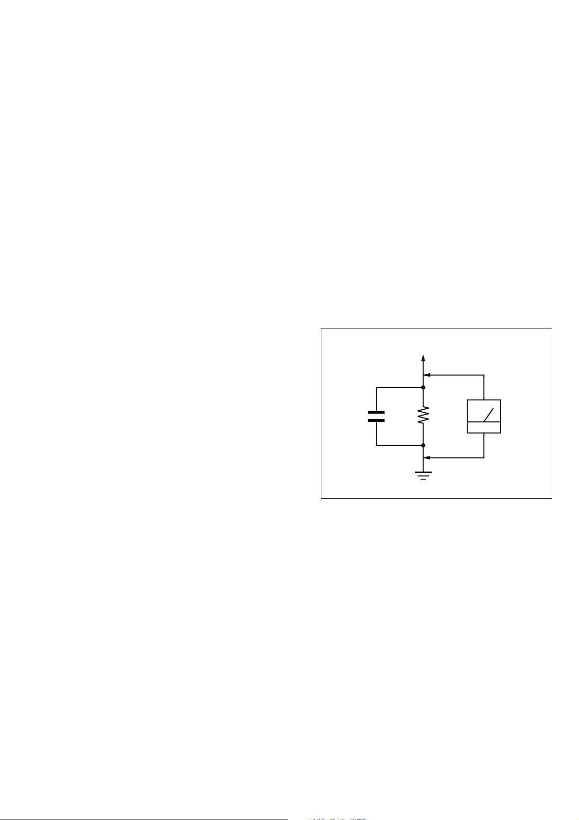
TABLE OF CONTENTS
SECTION 1
SERVICING NOTES
1. SERVICING NOTES............................................... 3
2. GENERAL
Location of Controls ....................................................... 4
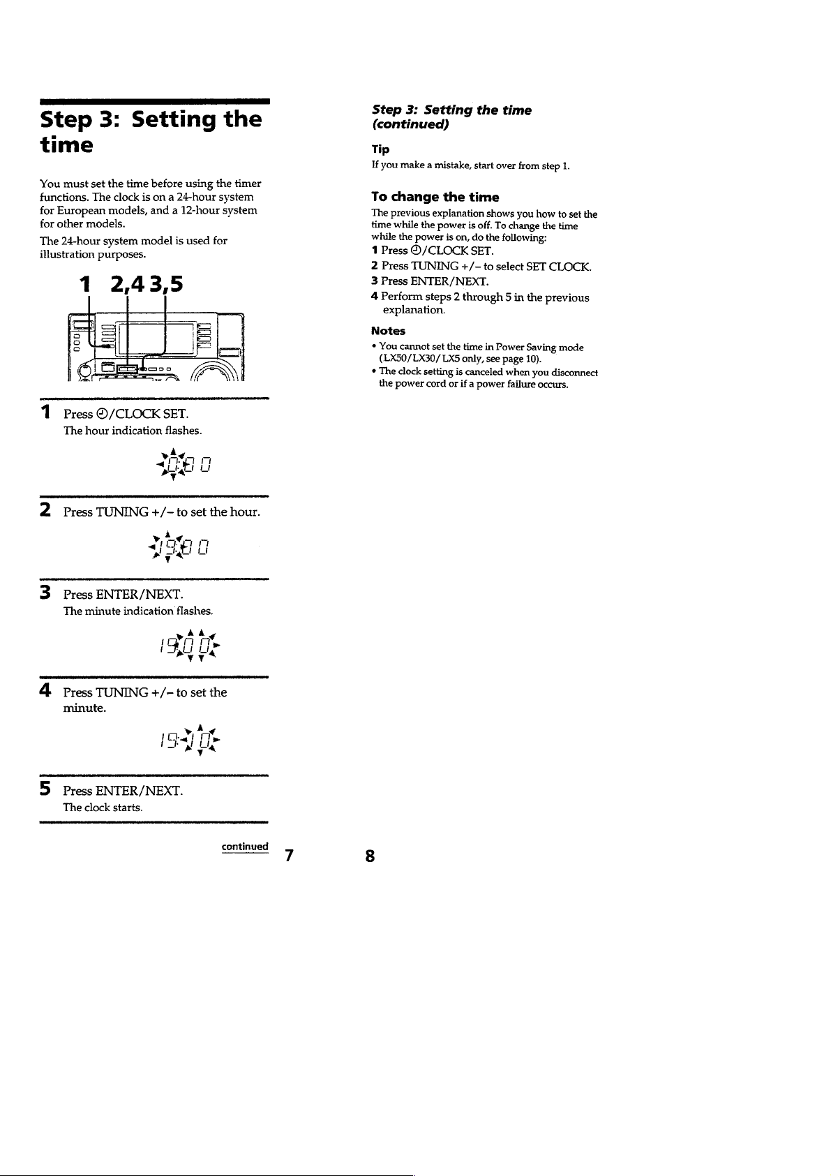
Setting the Time .............................................................. 6
3. DISASSEMBLY ......................................................... 7
4. DIAGRAMS
4-1. Note for Printed Wiring Boards and
Schematic Diagrams ....................................................... 11
4-2. Printed Wiring Board – BD Board – .............................. 12
4-3. Schematic Diagram – BD Board – ................................ 13
4-4. Printed Wiring Boards – CD MOTOR Section –.......... 14
4-5. Schematic Diagram – CD MOTOR Section – .............. 15
4-6. Printed Wiring Board – AUDIO Board – ...................... 16
4-7. Schematic Diagram – AUDIO Board – ......................... 17
4-8. Printed Wiring Board – LEAF SW Board –.................. 18
4-9. Schematic Diagram – LEAF SW Board –..................... 18
4-10. Printed Wiring Board – MAIN Board – ........................ 19
4-11. Schematic Diagram – MAIN Board (1/3) – .................. 20
4-12. Schematic Diagram – MAIN Board (2/3) – .................. 21
4-13. Schematic Diagram – MAIN Board (3/3) – .................. 22
4-14. Printed Wiring Board – PANEL FL Board –................. 24
4-15. Schematic Diagram – PANEL FL Board –.................... 25
4-16. Printed Wiring Board – PANEL VR Board –................ 26
4-17. Schematic Diagram – PANEL VR Board –................... 27
4-18. Printed Wiring Boards – TC-A/TC-B/CD-L/
CD-L2/CD-R/CD-R2 Boards – ...................................... 28
4-19. Schematic Diagram – TC-A/TC-B/CD-L/
CD-L2/CD-R/CD-R2 Boards – ...................................... 29
4-20. Printed Wiring Boards – FRONT INPUT/
HEADPHONE/MIC Boards – ........................................ 30
4-21. Schematic Diagram – FRONT INPUT/
HEADPHONE/MIC Boards – ........................................ 31
4-22. Printed Wiring Board – PA Board – .............................. 32
4-23. Schematic Diagram – PA Board – ................................. 33
4-24. Printed Wiring Boards – TRANS/SUB TRANS
(LX5/LX30/LX50) Boards – .......................................... 34
4-25. Schematic Diagram – TRANS/SUB TRANS
(LX5/LX30/LX50) Boards – .......................................... 35
SAFETY CHECK-OUT
After correcting the original service problem, perform the following safety check before releasing the set to the customer:
Check the antenna terminals, metal trim, “metallized” knobs,
screws, and all other exposed metal parts for AC leakage.
Check leakage as described below.
LEAKAGE TEST
The AC leakage from any exposed metal part to earth ground and
from all exposed metal parts to any exposed metal part having a
return to chassis, must not exceed 0.5 mA (500 microamperes.).
Leakage current can be measured by any one of three methods.
1. A commercial leakage tester , such as the Simpson 229 or RCA
WT -540A. Follo w the manufacturers’ instructions to use these
instruments.
2. A battery-operated AC milliammeter. The Data Precision 245
digital multimeter is suitable for this job.
3. Measuring the voltage drop across a resistor by means of a
VOM or battery-operated AC voltmeter. The “limit” indication is 0.75 V, so analog meters must have an accurate lowvoltage scale. The Simpson 250 and Sanwa SH-63Trd are examples of a passive VOM that is suitable. Nearly all battery
operated digital multimeters that have a 2 V A C range are suitable. (See Fig. A)
To Exposed Metal
Parts on Set
AC
1.5 k
0.15 µF
Fig. A. Using an AC voltmeter to check AC leakage.
Ω
Earth Ground
voltmeter
(0.75 V)
5. EXPLODED VIEWS................................................ 38
6. ELECTRICAL PARTS LIST ............................... 46
3
SECTION 2
GENERAL
This appliance is classified as a CLASS 1 LASER product.
The CLASS 1 LASER PRODUCT MARKING is located on
the rear exterior.
Laser component in this product is capable of emitting radiation
exceeding the limit for Class 1.
The following caution label is located inside the unit.
NOTES ON HANDLING THE OPTICAL PICK-UP
BLOCK OR BASE UNIT
The laser diode in the optical pick-up block may suffer electrostatic break-down because of the potential difference generated
by the charged electrostatic load, etc. on clothing and the human
body.
During repair, pay attention to electrostatic break-down and also
use the procedure in the printed matter which is included in the
repair parts.
The flexible board is easily damaged and should be handled with
care.
LOCATION OF CONTROLS
– Front Panel –
2 43
1
wf
wd
ws
wa
w;
ql
qk
qj
5
6
7
8
9
0
qa
qs
qd
qfqgqh
NOTES ON LASER DIODE EMISSION CHECK
The laser beam on this model is concentrated so as to be focused
on the disc reflective surface by the objective lens in the optical
pick-up block. Therefore, when checking the laser diode emission, observe from more than 30 cm away from the objective lens.
Notes on chip component replacement
• Never reuse a disconnected chip component.
• Notice that the minus side of a tantalum capacitor may be damaged by heat.
Flexible Circuit Board Repairing
• Keep the temperature of the soldering iron around 270 ˚C during repairing.
• Do not touch the soldering iron on the same conductor of the
circuit board (within 3 times).
• Be careful not to apply force on the conductor when soldering
or unsoldering.
CAUTION
Use of controls or adjustments or performance of procedures
other than those specified herein may result in hazardous radiation exposure.
– Rear Panel –
2
1
9
8
7
6
5
4 3
4

1 ?/1 (POWER) button
2 DAILY button
REC button
SLEEP button
c/CLOCK SET button
3 Display
4 SYNC EQ button
SYNC BASS button
SURROUND button
MIX GUITAR/KARAOKE button
5 FUNCTION button
6 v/B/V/b button
7 VOLUME control
8 DECK B
9 PHONES jack
0 DECK B operating button
g button G button x button
m button M button X button
z REC button HI SPEED DUB button
CD SYNC button
qa . AMS > control
qs CD operating button
G X button x button m button
M button DISC SKIP button
qd VIDEO 2 INPUT jack
qf PLAY MODE button
REPEAT button
qg Z A EJECT
Z B EJECT
qh DISC1-5 button
qj LOOP button
FLASH button
NON-STOP button
EDIT button
qk DECK A operating button
g button G button x button
m button M button
DIRECTION button
DOLBY NR button
ql MIC MIX jack
GUITAR jack
w; DECK A
wa SUPPER WOOFER MODE button
MIC LEVEL control
GUITAR LEVEL control
ws EJECT button
GROOVE button
SUPER WOOFER button
wd TUNER/BAND button
TUNING +/– button
ENTER/NEXT button
TUNER MEMORY button
STEREO/MONO button
TUNING MODE button
PTY button (LX5 only)
wf POWER SAVE/DEMO (STAND BY) button
DISPLAY button
SPECTRUM ANALYZER button
1 DJ MIX jack
2 ANTENNA terminal
3 REAR SURROUND SPEAKER terminal (LX50 only)
4 FRONT SPEAKER terminal
5 CD DIGITAL OUT terminal
6 VIDEO OUT jack
7 VIDEO 1 jack
8 MD IN/OUT jack
9 PHONO IN jack
5
6
SECTION 3
)
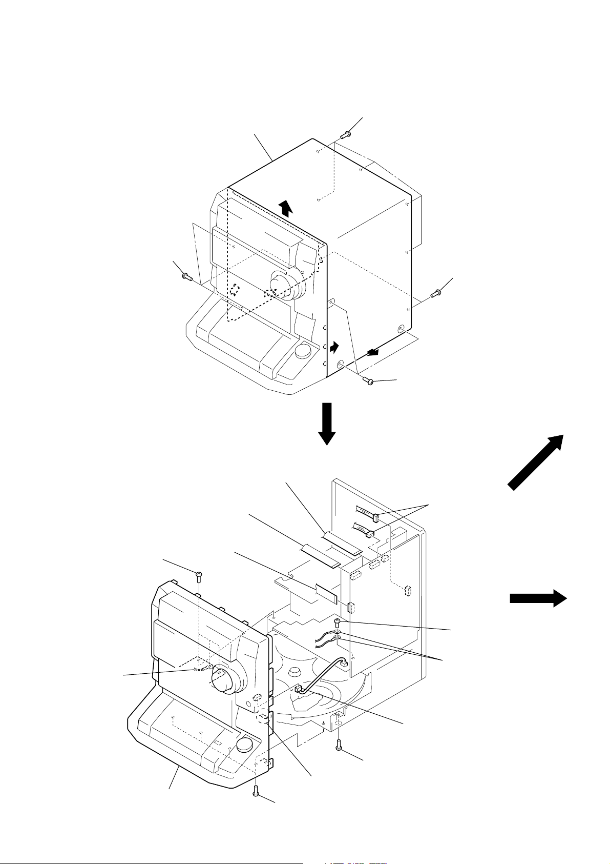
DISASSEMBLY
Note: Follow the disassembly procedure in the numerical order given.
CASE
6 case
1 three screws
(CASE3 TP2)
4
5
2 five screws
(BVTT3 × 6)
3 two screws
(BVTP3 × 8)
FRONT PANEL SECTION
1 wire (flat type)
3 three screws
(BVTP3 × 8)
1 wire (flat type)
1 wire (flat type)
(17 core) (CN304)
(13 core) (CN431)
(15 core) (CN303)
5
4
1 three screws
(CASE3 TP2)
2 two connectors
(CN452, 702)
MAIN BOARD (Page 8)
CD MECHANISM DECK
(Page 9)
3 screw
(BVTP3 × 8
4 lug
4 two lugs
2 connector
(CN802)
5 screw (BVTP3 × 8)
6 claw
7 front panel section
5 four screws
(BVTP3 × 8)
7
TAPE MECHANISM DECK (TCM-230PWR1)
2 two screws
(BVTP3 × 8)
1 wire (flat type) (17 core)
(CN1001)
1 wire (flat type) (15 core)
(CN601)
2 two screws
(BVTP3 × 8)
3 tape mechanism deck
(TCM-230PWR1)
MAIN BOARD
7 wire (flat type) (19 core)
(CN411)
6 back panel
2 nine screws
(BVTP3 × 8)
1 wire (flat type) (15 core) (LX5)
wire (flat type) (13 core) (LX6/LX30/LX50)
(CN441)
4
3 jumper plug
(LX5/LX6: Mexican/LX30/LX50)
2 screw (BVTP3 × 8)
(LX5/LX6: Mexican/
LX30/LX50)
2 three screws (BVTP3 × 8)
2 screw (BVTP3 × 8)
(LX50)
2 two screws (BVTP3 × 8)
5 connector (CN903)
qa MAIN board
9 two screws
(BVTP3 × 8)
8 connector
(CN412)
0 two connector
(CN803, 804)
8
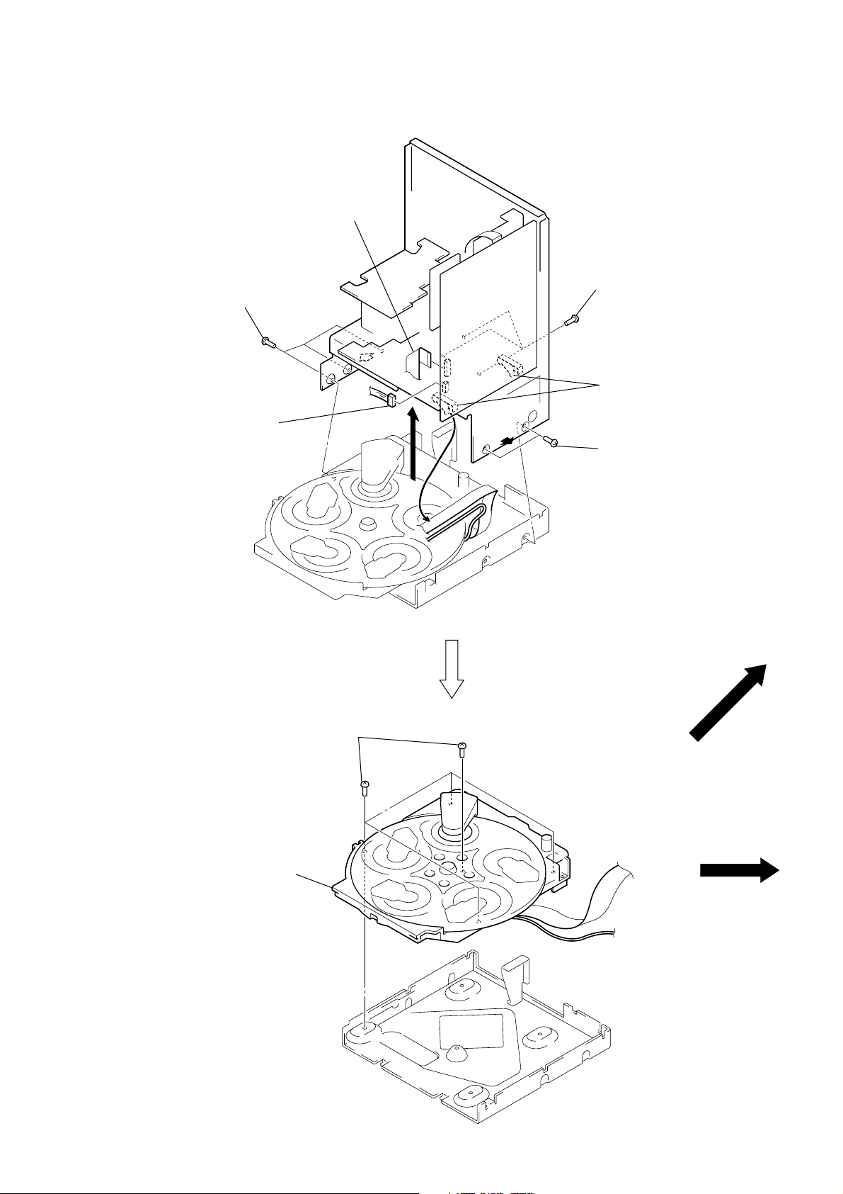
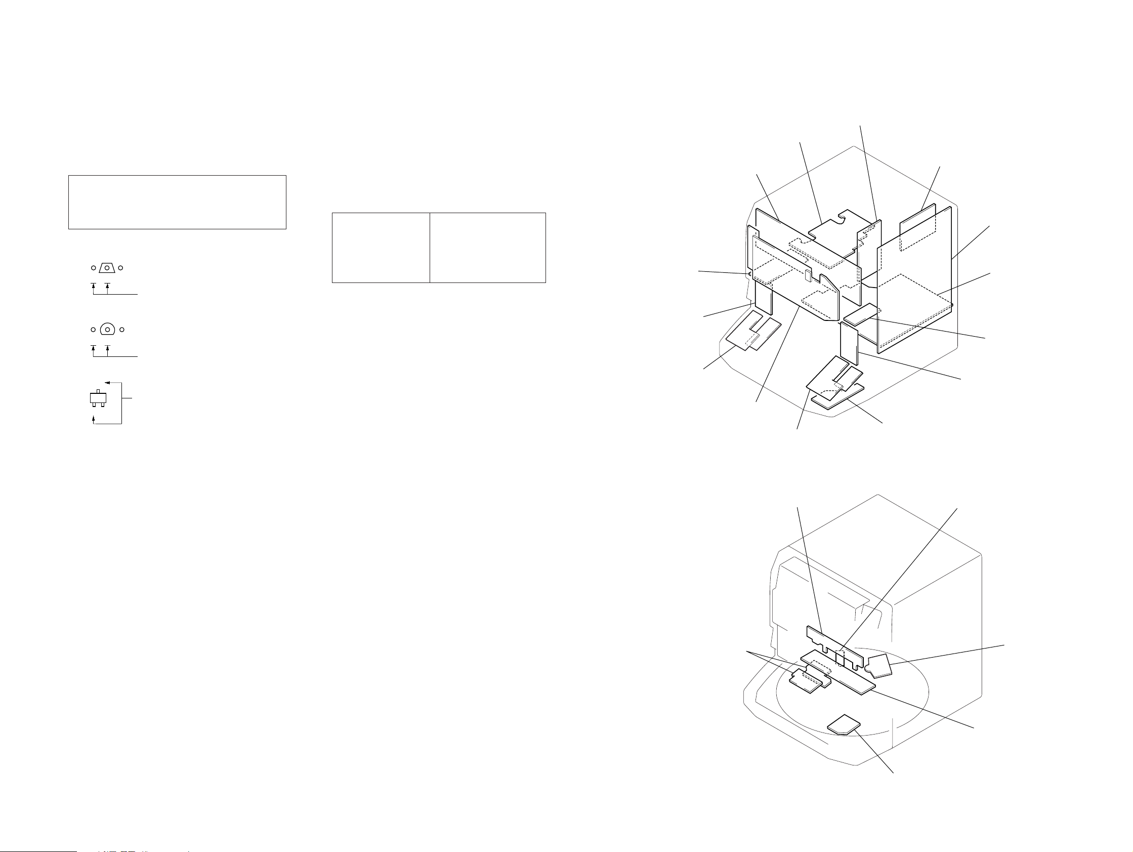
CD MECHANISM DECK (CDM37M-5BD32L)
1 wire (flat type) (19 core)
(CN411)
3 three screws
(BVTP3 × 8)
2 connector
(CN412)
4
6
3 three screws
(BVTP3 × 8)
5 Open the two cable clamps.
4
3 two screws
(BVTP3 × 8)
7 five screws
8 CD mechanism deck
(CDM37M-5BD32L)
(BVTP3 × 8)
9
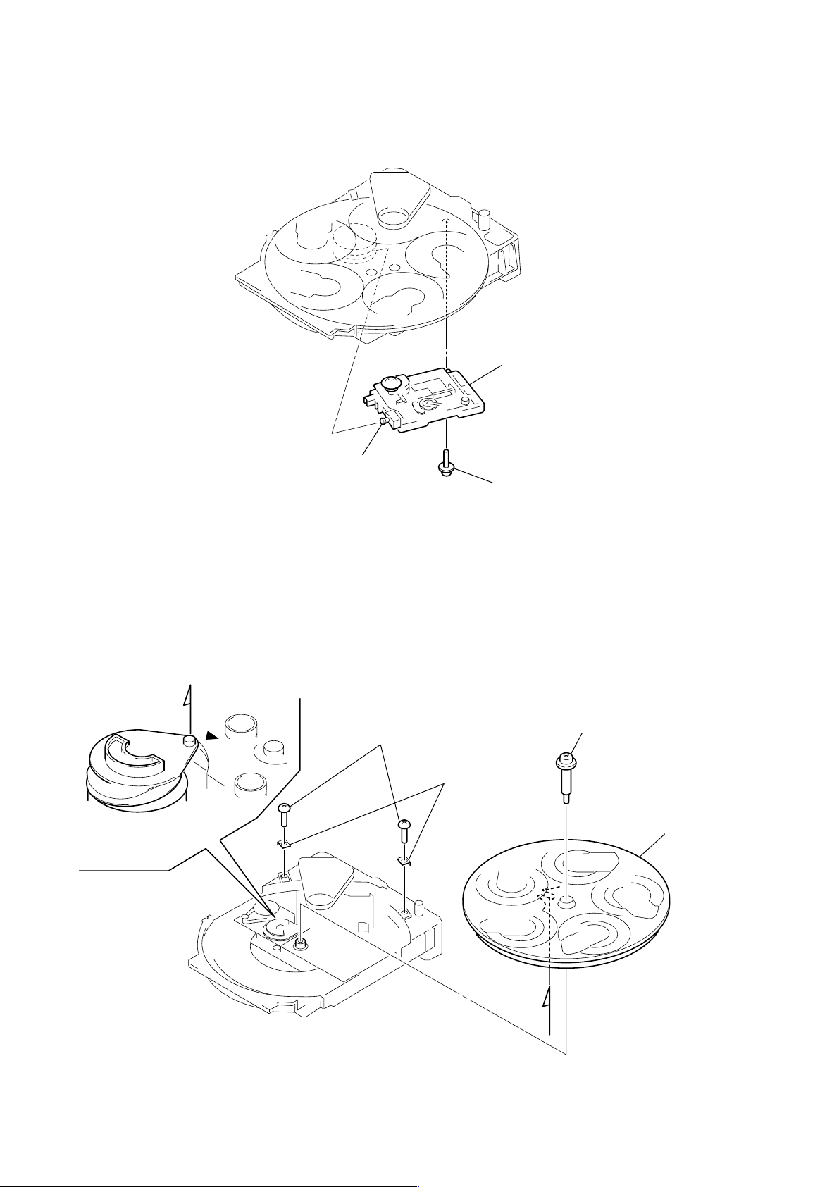
BASE UNIT (BU-5BD32L)
w
e
3 base unit
(BU-5BD32L)
2 boss
1 BU fitting scre
DISC TABLE
Note: When the disc table is installed, adjust the positions of roller cam
and mark B as shown in the figure, then set to the groove of disc
table.
A
1 two screws
(BVTP3 × 8)
3 step screw
2 two brackets (BU)
4 disc tabl
A
10
SECTION 4
d
d
DIAGRAMS
4-1. NOTE FOR PRINTED WIRING BOARDS AND SCHEMATIC DIAGRAMS
(In addition to this, the necessary note is printed in each block)
Note on Printed Wiring Board:
• X : parts extracted from the component side.
• Y : parts extracted from the conductor side.
f
•
• b : Pattern from the side which enables seeing.
(The other layers' patterns are not indicated.)
Caution:
Pattern face side: Parts on the pattern face side seen from
(Side B) the pattern face are indicated.
Parts face side: Parts on the parts face side seen from
(Side A) the parts face are indicated.
• Indication of transisitor.
: internal component.
Q
B
CE
These are omitted.
Q
B
CE
These are omitted.
C
Q
B
E
These are omitted.
Note on Schematic Diagram:
• All capacitors are in µF unless otherwise noted. pF: µµF
50 WV or less are not indicated except for electrolytics
and tantalums.
• All resistors are in Ω and 1/
specified.
f
•
• 2 : nonflammable resistor.
• 5 : fusible resistor.
• C : panel designation.
• U : B+ Line.
• V : B– Line.
• H : adjustment for repair.
• Voltages are tak en with a V OM (Input impedance 10 MΩ).
• Waveforms are taken with a oscilloscope.
• Circled numbers refer to waveforms.
• Signal path.
• Abbreviation
: internal component.
Note:
The components identified by mark 0 or dotted
line with mark 0 are critical for safety.
Replace only with part
number specified.
Voltage variations may be noted due to normal production tolerances.
Voltage variations may be noted due to normal production tolerances.
F : TUNER (FM/AM)
E : PLAYBACK (DECK A)
d : PLAYBACK (DECK B)
G : RECORD
J : CD PLAY (ANALOG OUT)
c : CD PLAY (DIGITAL OUT)
N : MIC INPUT
AUS : Australian model
AR : Argentine model
EA : Saudi Arabia model
MY : Malaysia model
MX : Mexican model
SP : Singapore model
4
Note:
Les composants identifiés par
une marque 0 sont critiques
pour la sécurité.
Ne les remplacer que par une
pièce portant le numéro
spécifié.
W or less unless otherwise
• Circuit Boards Location
MIC board
TC-A board
CD-L board
TRANS board
PANEL FL board
P ANEL VR board
CD-R board
LEAF SW board
SUB TRANS board
(LX5/LX30/LX50)
TUNER (FM/AM)
MAIN board
PA board
HEADPHONE boar
TC-B board
FRONT INPUT board
TABLE SENSOR board
CD MOTOR board
BD boar
AUDIO board
LED board
1111
HCD-LX5/LX6/LX30/LX50
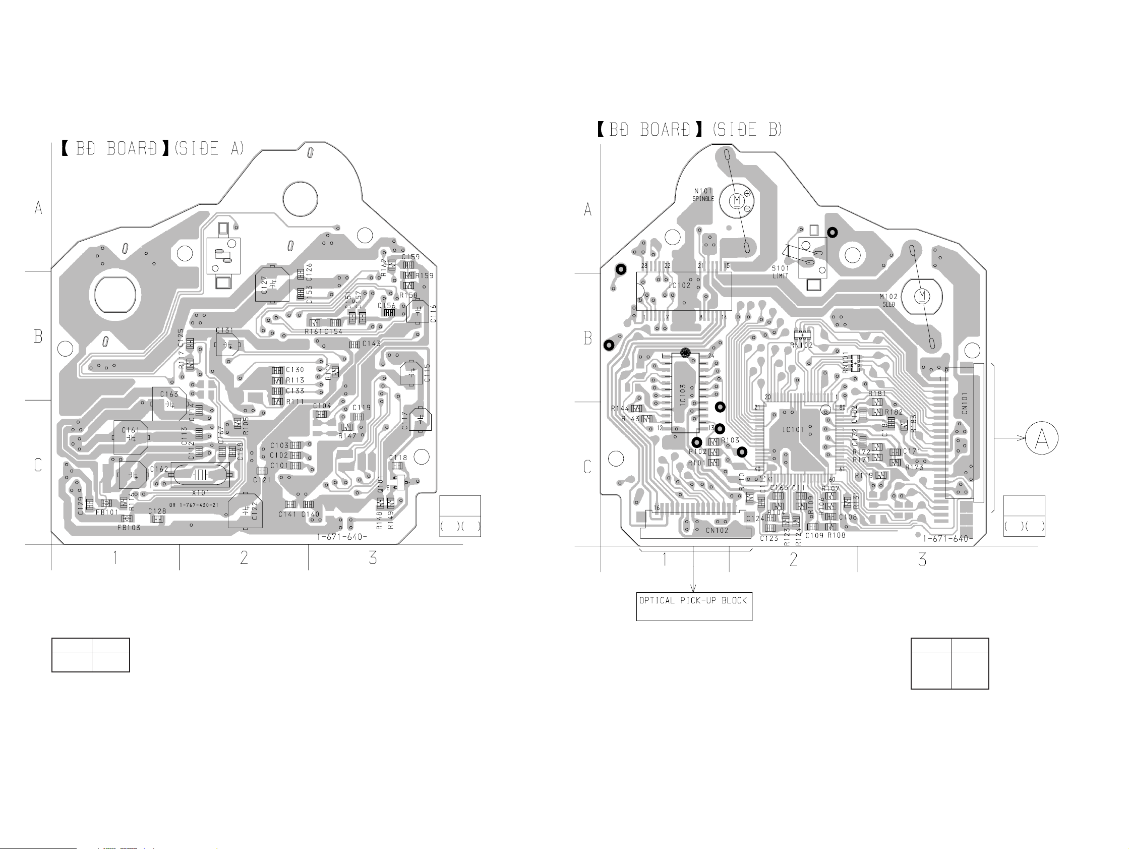
4-2. PRINTED WIRING BOARD – BD Board – • See page 11 for Circuit Boards Location.
)(
TP(GND)
TP(VC)
TP(RF)
TP
(AGCCON)
TP(FE)
TP(TE)
TP(FE1)
21
31
31,,
21
05
05
)(
)(
(Page 19)
19
21
21
31
31,,
• Semiconductor
Location
(Side A)
Ref. No. Location
Q101 C-3
KSS-213D/Q-NP
• Semiconductor
Location
(Side B)
Ref. No. Location
IC101 C-2
IC102 B-1
IC103 B-1
1212
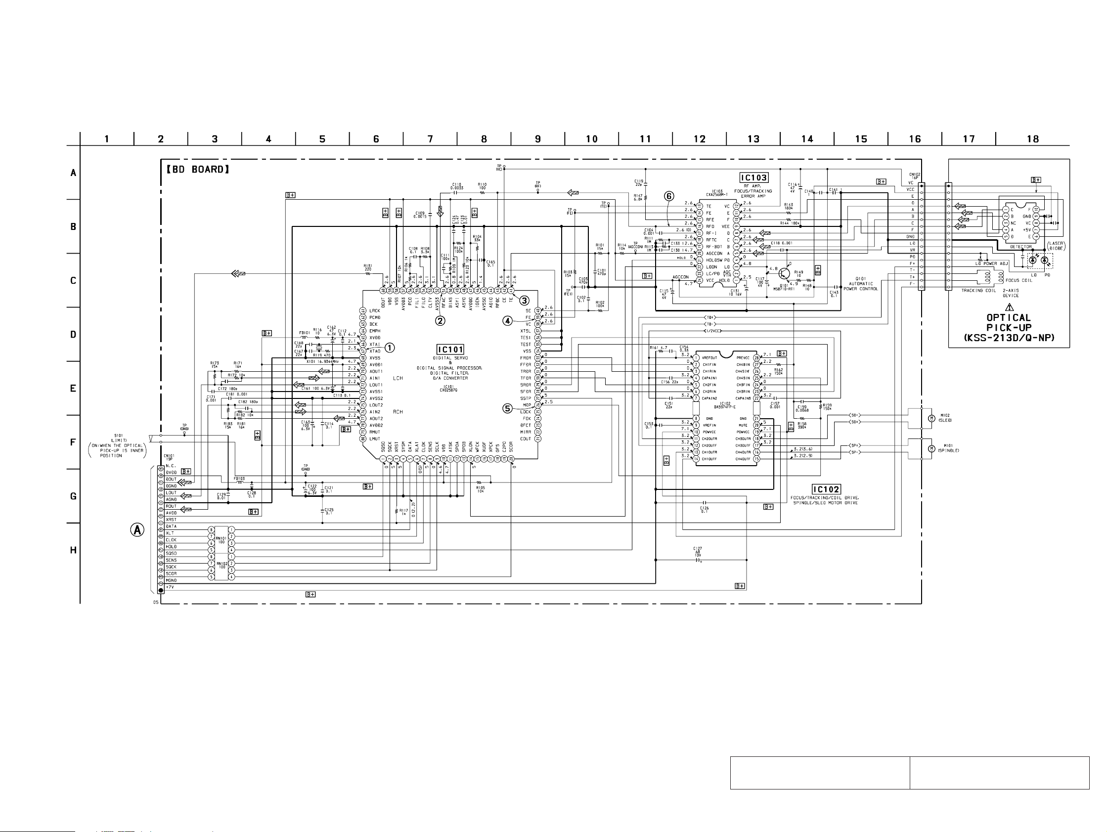
4-3. SCHEMATIC DIAGRAM – BD Board – • See page 23 for Waveforms. • See page 36 for IC Block Diagrams.
HCD-LX5/LX6/LX30/LX50
(Page 21)
• Voltages and waveforms are dc with respect to ground
under no-signal conditions.
no mark : CD STOP
( ) : CD PLAY
The components identified by mark 0 or dotted
line with mark 0 are critical for safety.
Replace only with part number specified.
Les composants identifiés par une marque 0 sont
critiques pour la sécurité. Ne les remplacer que
par une pièce portant le numéro spécifié.
1313
HCD-LX5/LX6/LX30/LX50
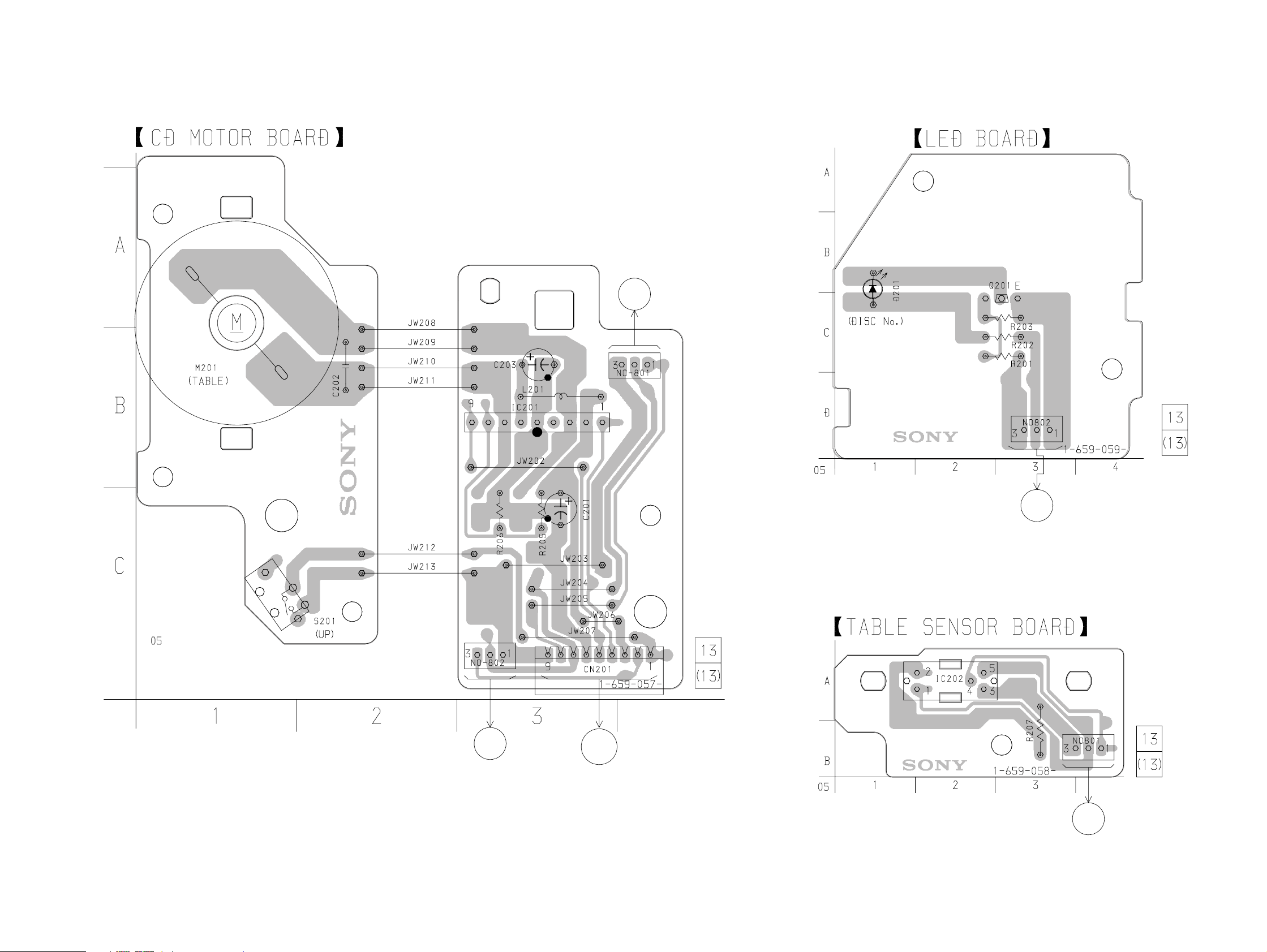
4-4. PRINTED WIRING BOARDS – CD MOTOR Section – • See page 11 for Circuit Boards Location.
TABLE SENSOR BOARD
TO
D
C
TO
CD MOTOR BOARD
C
LED BOARD
B
(Page 19)TO
D
TO
CD MOTOR BOARD
1414
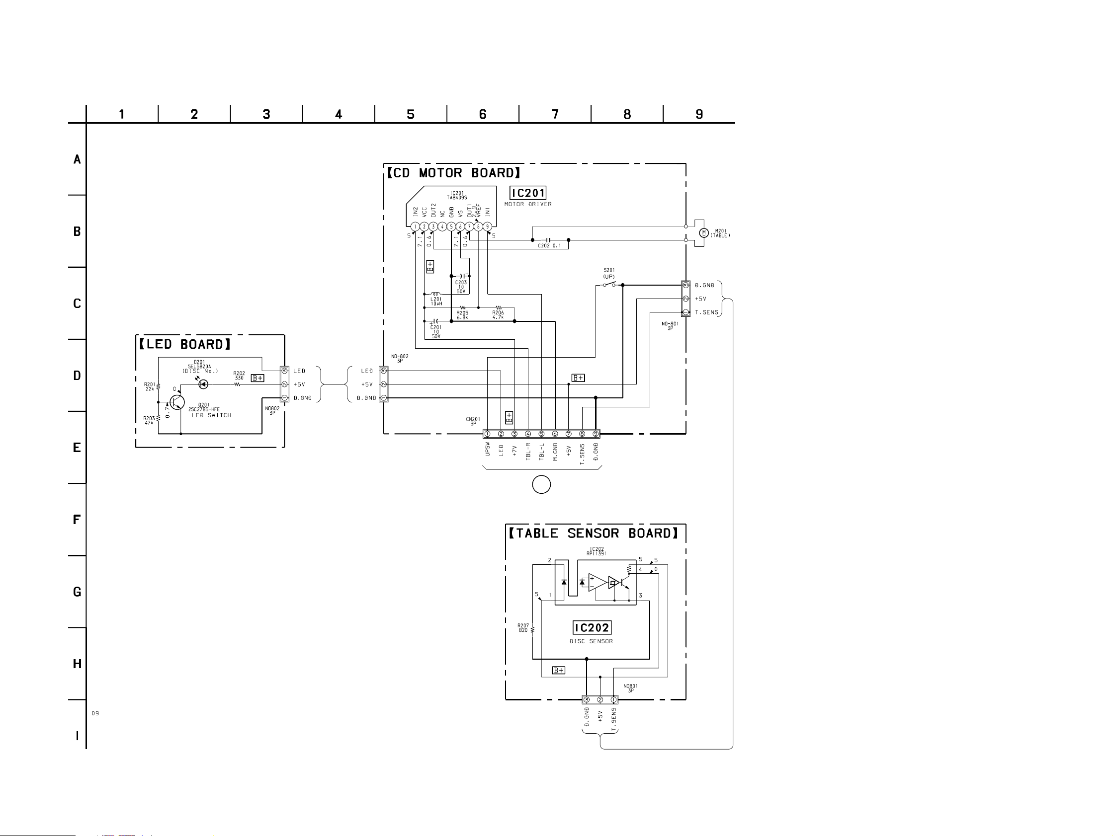
4-5. SCHEMATIC DIAGRAM – CD MOTOR Section – • See page 36 for IC Block Diagrams.
HCD-LX5/LX6/LX30/LX50
B
(Page 21)
• Voltages are dc with respect to ground under no-signal
conditions.
no mark : CD STOP
1515
HCD-LX5/LX6/LX30/LX50
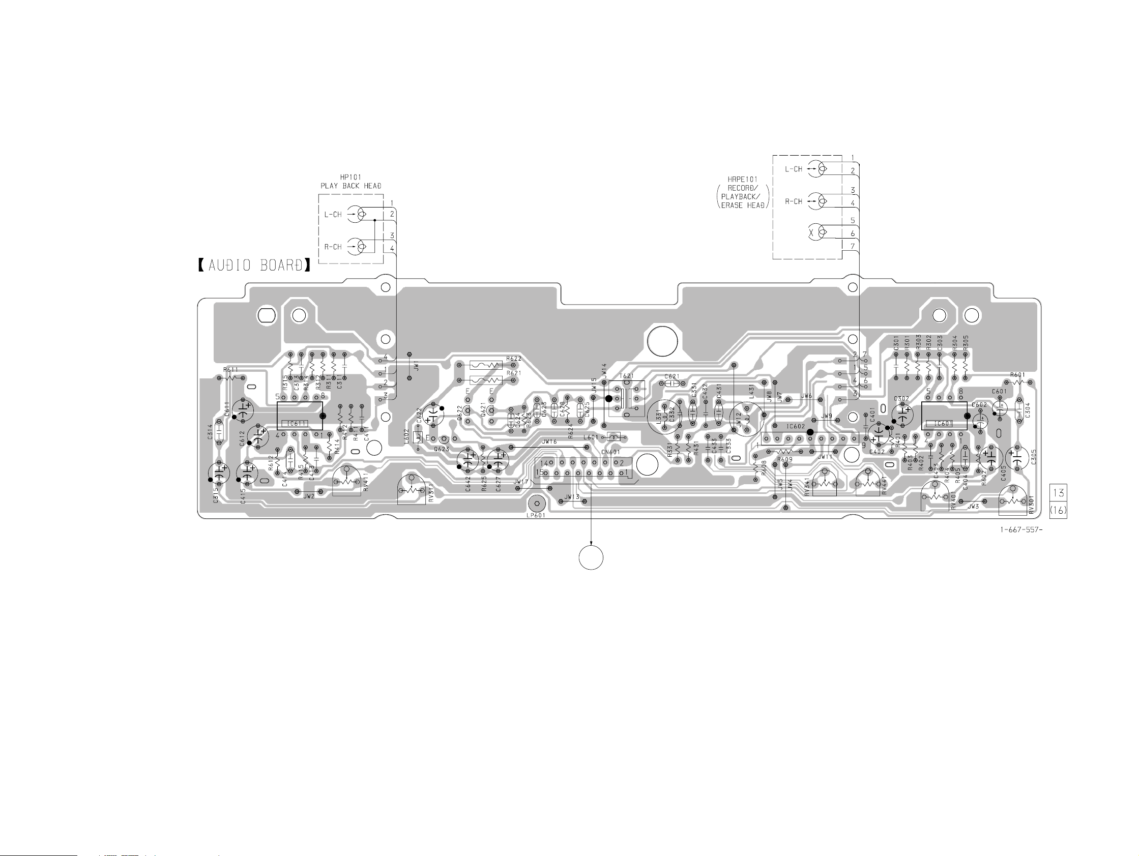
4-6. PRINTED WIRING BOARD – AUDIO Board – • See page 11 for Circuit Boards Location.
(
)
05
E
(Page 19)
1616
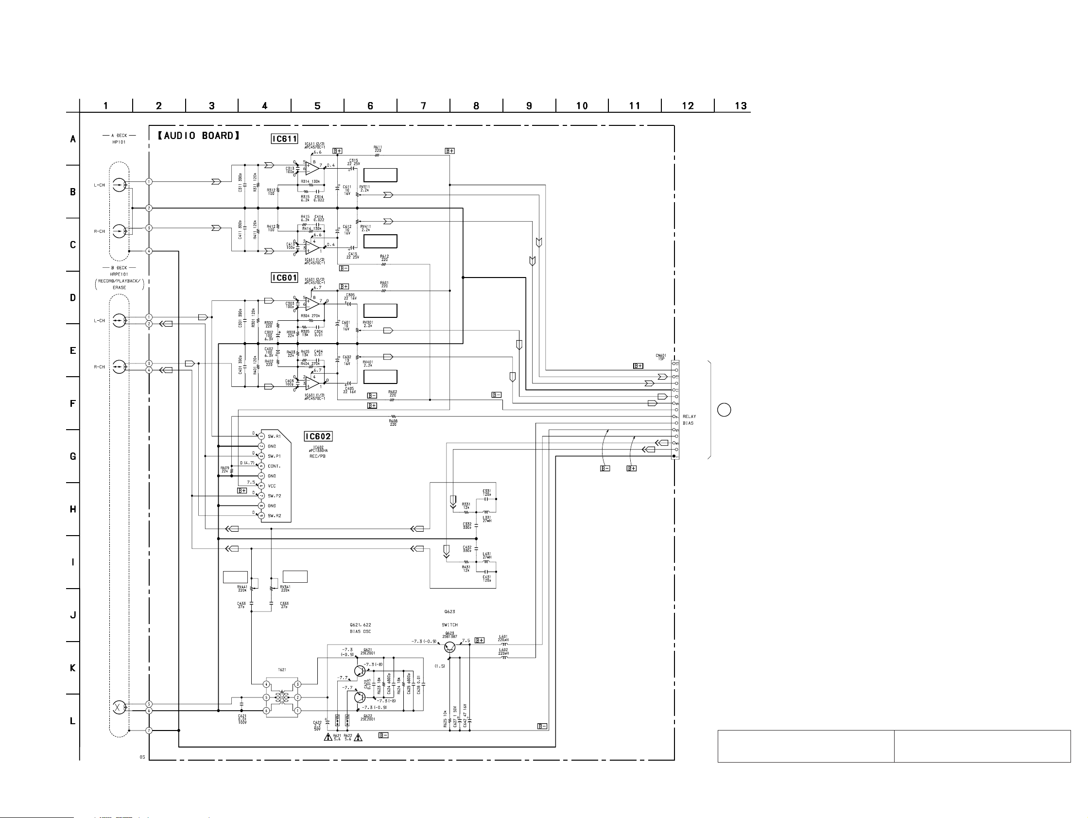
4-7. SCHEMATIC DIAGRAM – AUDIO Board – • See page 36 for IC Block Diagrams.
HCD-LX5/LX6/LX30/LX50
(PLAYBACK)
PB EQ AMP
(DECK A)
PB EQ AMP
(DECK B)
SWITCHING
PB LEVEL (L)
(DECK A)
PB LEVEL (R)
(DECK A)
PB LEVEL (L)
(DECK B)
PB LEVEL (R)
(DECK B)
NC
A +7.5V
APB–LCH
APB–RCH
AGND
BPB–LCH
BPB–RCH
A –7.5V
–VBIAS (–7.5V)
+VBIAS (+7.5V)
B–REC–RCH
B–REC–LCH
TC–HEAD–GND
E
(Page21)
REC BIAS (R)
(DECK B)
BIAS OSC
REC BIAS (L)
(DECK B)
-6.8
REC BIAS
• Voltages are dc with respect to ground under no-signal
conditions.
no mark : TAPE PLAY
( ) : RECORD
The components identified by mark 0 or dotted
line with mark 0 are critical for safety.
Replace only with part number specified.
Les composants identifiés par une marque 0 sont
critiques pour la sécurité. Ne les remplacer que
par une pièce portant le numéro spécifié.
1717
HCD-LX5/LX6/LX30/LX50
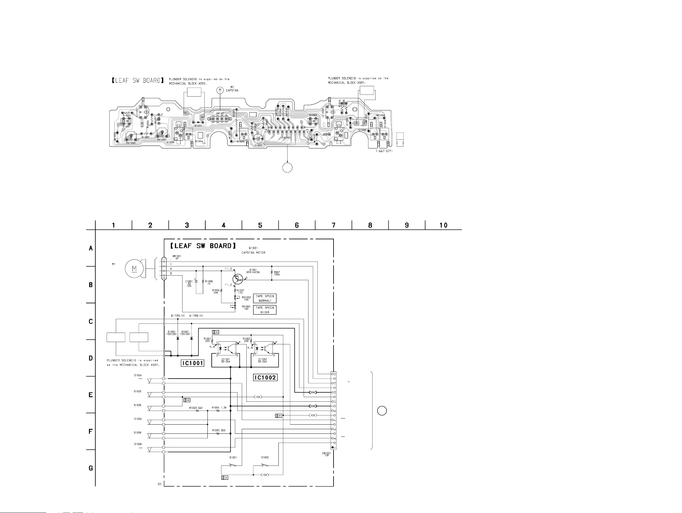
4-8. PRINTED WIRING BOARD – LEAF SW Board – • See page 11 for Circuit Boards Location.
DECK A
PLUNGER
4
3
1
2
(DECK A PLAY)
05
(DECK A HALF)
(DECK A 120/70)
(
4-9. SCHEMATIC DIAGRAM – LEAF SW Board –
)
(DECK A REC)
CONTROL SWITCH
F
(Page 19)
(DECK B PLAY)
4
1
(DECK B HALF)
DECK B
PLUNGER
3
2
(DECK B 120/70)
(DECK B REC)
12
12
(CAPSTAN)
DECK B
PLUNGER
DECK A
PLUNGER
(DECK A 120/70)
(DECK A HALF)
(DECK A REC)
(DECK B HALF)
(DECK B REC)
(DECK B 120/70)
ROTATION DETECT SENSOR
(DECK A)
ROTATION DETECT
SENSOR (DECK B)
CAPM–
CAPM+
CAPM–H/L
A–TRGM
TRGM–GND
B–TRGM
A–SHUT
DGND
A–HALF
+5V
A–120/70
B–SHUT
A PLAY
B–HALF / REC–A / REC–B
B–120/70
B PALY
NC
F
(Page 21)
(DECK A PLAY)
(DECK B PLAY)
• Voltages are dc with respect to ground under no-signal
conditions.
no mark : TAPE PLAY
( ) : RECORD
: Impossible to measure
∗
1818
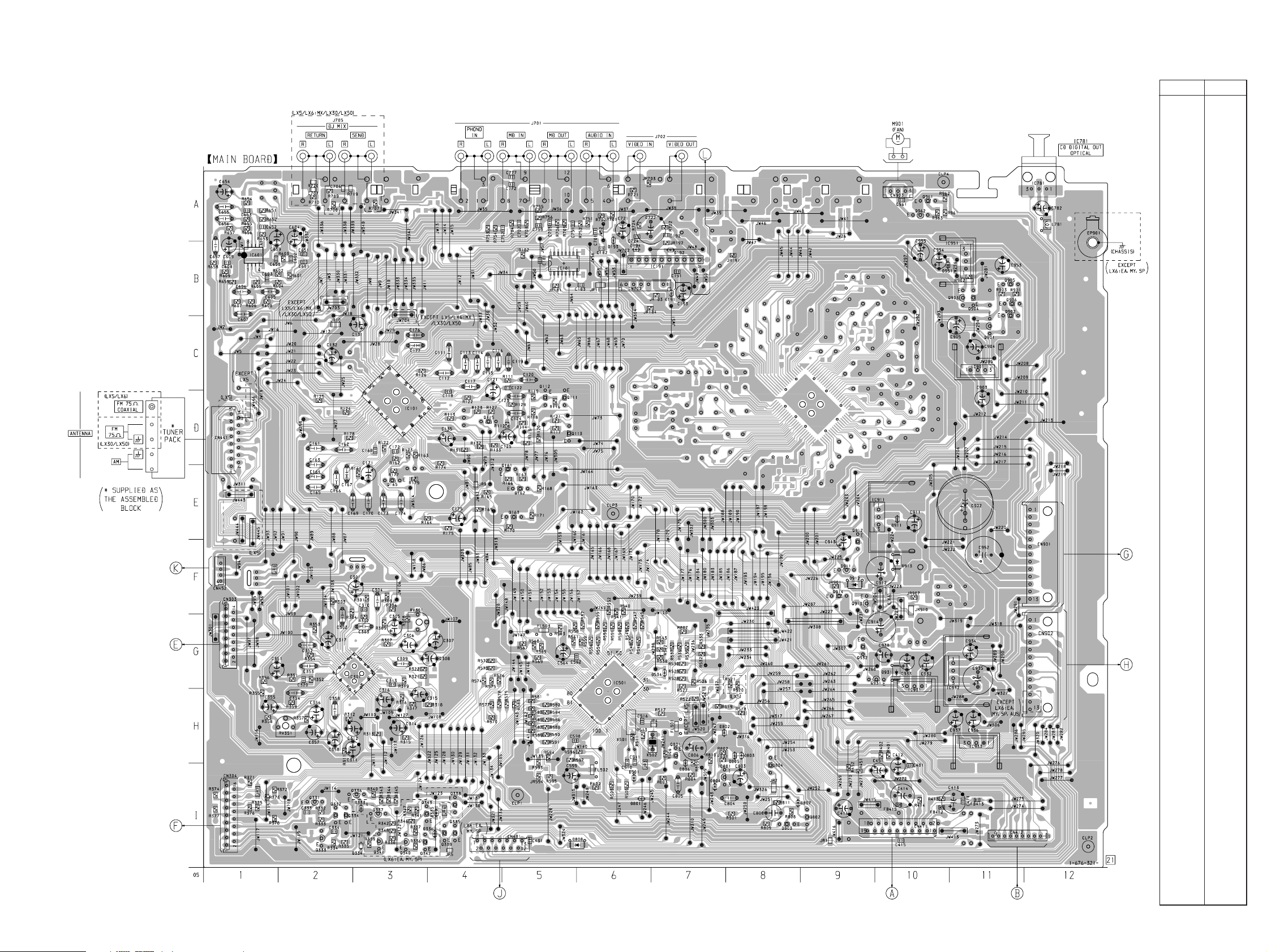
4-10. PRINTED WIRING BOARD – MAIN Board – • See page 11 for Circuit Boards Location.
(Page 30)
HCD-LX5/LX6/LX30/LX50
• Semiconductor
Location
Ref. No. Location
D191 B-7
D192 B-7
D193 A-6
D194 B-6
D333 I-3
D334 I-3
D335 I-4
D336 I-4
D501 I-6
D534 G-7
D801 I-6
D802 H-7
D803 H-8
D804 I-7
D805 H-8
D806 H-7
D807 H-8
D808 I-6
D911 E-10
D912 F-9
D913 F-10
D931 G-10
D951 B-10
IC101 D-3
IC181 B-5
IC191 B-7
IC301 G-2
IC501 H-6
IC601 B-1
IC781 A-12
IC801 I-7
IC901 C-11
IC911 E-10
IC931 G-10
IC932 G-11
IC932 G-12
IC933 H-11
IC951 B-11
(Page 26)
(Page 16)
(Page 18)
(Page 24)
Q111 D-5
Q112 D-5
Q113 D-5
Q115 D-4
Q161 E-5
(Page 32)
(Page 32)
(Page 14)(Page 12)
Q162 E-5
Q163 E-5
Q165 E-3
Q331 I-2
Q332 I-2
Q333 I-2
Q334 I-2
Q335 I-4
Q336 I-3
Q337 I-3
Q338 I-4
Q339 I-4
Q340 I-3
Q341 I-3
Q342 I-3
Q343 I-3
Q801 H-7
Q802 H-9
Q803 H-8
Q804 I-8
Q901 C-11
Q902 B-11
Q903 B-11
Q904 B-11
Q905 B-11
Q906 B-11
Q911 F-9
Q912 F-9
Q913 F-9
Q914 F-9
Q931 G-10
Q932 G-9
Q961 A-10
Q962 A-10
1919
 Loading...