

Sony HCD-LV100AV Service manual
Amplifier section
Front Speaker:
The following measured at AC 120/220/240 V,
50Hz
DIN power output (Rated)
150 + 150 watts
(6 ohms at 1 kHz, DIN)
Continuous RMS power output (Reference)
200 + 200 watts
(6 ohms at 1 kHz, 10%
THD)
Center Speaker:
DIN power output (Rated)
35 watts
(8 ohms at 1 kHz, DIN)
Continuous RMS power output (Reference)
50 watts
(8 ohms at 1 kHz, 10%
THD)
Rear Speaker:
DIN power output (Rated)
35 + 35 watts
(8 ohms at 1 kHz, DIN)
Continuous RMS power output (Reference)
50 + 50 watts
(8 ohms at 1 kHz, 10%
THD)
Inputs
PHONO IN (phono jacks):sensitivity 3 mV,
impedance 47 kilohms
MIC 1/2 (phone jack): sensitivity 1 mV,
impedance 10 kilohms
VIDEO1 IN (phono jacks):sensitivity 250 mV,
impedance 47 kilohms
VIDEO2 IN (phono jacks):sensitivity 250 mV,
impedance 47 kilohms
MD IN (phono jacks): sensitivity 450 mV,
impedance 47 kilohms
DVD INPUT
FRONT, REAR, CENTER, WOOFER (phono jacks):
sensitivity 450 mV,
impedance 47 kilohms
Outputs
PHONES (stereo phone jack):
accepts headphones of 8
ohms or more
VIDEO OUT (phono jack):
voltage 250 mV,
impedance 1 kilohm
MD OUT (phono jacks): voltage 250 mV,
impedance 1 kilohm
WOOFER OUT (phono jack):
voltage 1 V, impedance
1 kilohm
FRONT SPEAKER: accepts impedance of 6 to
16 ohms
CENTER SPEAKER: accepts impedance of 8 to
16 ohms
REAR SPEAKER: accepts impedance of 8 to
16 ohms
Video section
Inputs
VIDEO1 IN (phono jacks):1 V p-p, 75 ohms
VIDEO2 IN (phono jacks):1 V p-p, 75 ohms
Outputs
VIDEO OUT (phono jack):1 V p-p, 75 ohms
S-VIDEO OUT (4-pin/mini-DIN jack):
Y: 1V p-p, unbalanced,
Sync negative,
C: 0.286 V p-p,
load impedance 75 ohms
VIDEO CD/CD player section
System Compact disc and digital
audio system
Laser Semiconductor laser
( = 780 nm)
Emission
duration: continuous
Laser output Max. 44.6 W*
* This output is the value
measured at a distance of
200 mm from the
objective lens surface on
the Optical Pick-up Block
with 7 mm aperture.
Wavelength 780 – 790 nm
Frequency response 2 Hz – 20 kHz (±0.5 dB)
Signal-to-noise ratio More than 90 dB
Dynamic range More than 90 dB
Video color system format
NTSC, PAL
HCD-LV100AV
SERVICE MANUAL
• HCD-LV100AV is the Amplifier, CD player,
Tape Deck and Tuner section in LBT-LV100AV.
Manufactured under license from Dolby
Laboratories Licensing Corporation.
“DOLBY” and the double-D symbol ; are
trademarks of Dolby Laboratories Licensing
Corporation.
CD CD Mechanism Type CDM37L-5BD34L
Section Base Unit Name BU-5BD34L
Tape deck Model Name Using Similar Mechanism NEW
Section Tape Transport Mechanism Type TCM-230PWR12
E Model
Model Name Using Similar Mechanism HCD-VR90AV
Optical Pick-up Name KSS-213D/Q-NP
SPECIFICATIONS
COMPACT Hi-Fi STEREO SYSTEM
— Continued on next page —
CD DIGITAL OUT
(square optical connector jack, rear panel)
Wave length: 660 nm
Output level: –18 dBm
Tape player section
Recording system 4-track 2-channel stereo
Frequency response (DOLBY NR OFF)
Tuner section
FM stereo, FM/AM superheterodyne tuner
FM tuner section
Tuning range 87.5 – 108.0 MHz (50 kHz
Antenna FM wire antenna
Antenna terminals 75 ohm unbalanced
Intermediate frequency 10.7 MHz
AM tuner section
Tuning range
Middle Eastern model: 531 – 1,602 kHz
Other models: 531 – 1,602 kHz
Antenna AM loop antenna,
Intermediate frequency 450 kHz
40 – 13,000 Hz (±3 dB),
using a Sony TYPE I
cassette
40 – 14,000 Hz (±3 dB),
using a Sony TYPE II
cassette
step)
(with the tuning interval
set at 9 kHz)
(with the tuning interval
set at 9 kHz)
530 – 1,710 kHz
(with the tuning interval
set at 10 kHz)
External antenna
terminals
General
Power requirements 120 V, 220 V, or 230 –
Power consumption 230 watts
Dimensions (w/h/d) Approx. 356 × 423 × 446
Mass Approx. 15.7 kg
Supplied accessories AM loop antenna (1)
Design and specifications are subject to change
without notice.
240 V AC, 50/60 Hz
Adjustable with voltage
selector
mm incl. projecting parts
and controls
FM wire antenna (1)
Speaker cords (2)
Remote (1)
R6 (size AA) batteries (2)
MODEL IDENTIFICATION
— BACK PANEL —
Parts No.
PARTS No.
MODEL
4-227-751-4π MY, SP
4-227-751-5π EA
4-227-751-7π IA
• Abbreviation
EA : Saudi Arabia model.
SP : Singapore model.
MY : Malaysia model.
IA : Indonesian model.
SAFETY CHECK-OUT
After correcting the original service problem, perform the following safety
checks before releasing the set to the customer.
1. Check the area of your repair for unsoldered or poorly-soldered
connections. Check the entire board surface for solder splashes
and bridges.
2. Check the interboard wiring to ensure that no wires are
"pinched" or contact high-wattage resistors.
3. Look for unauthorized replacement parts, particularly
transistors, that were installed during a previous repair . Point
them out to the customer and recommend their replacement.
4. Look for parts which, through functioning, show obvious signs
of deterioration. Point them out to the customer and
recommend their replacement.
SAFETY-RELATED COMPONENT WARNING!!
COMPONENTS IDENTIFIED BY MARK 0 OR DOTTED LINE WITH
MARK 0 ON THE SCHEMATIC DIAGRAMS AND IN THE PARTS
LIST ARE CRITICAL TO SAFE OPERATION. REPLACE THESE
COMPONENTS WITH SONY PARTS WHOSE PART NUMBERS
APPEAR AS SHOWN IN THIS MANUAL OR IN SUPPLEMENTS
PUBLISHED BY SONY.
5. Check the B+ voltage to see it is at the values specified.
6. Flexible Circuit Board Repairing
• Keep the temperature of the soldering iron around 270˚C
during repairing.
• Do not touch the soldering iron on the same conductor of the
circuit board (within 3 times).
• Be careful not to apply force on the conductor when soldering
or unsoldering.
2
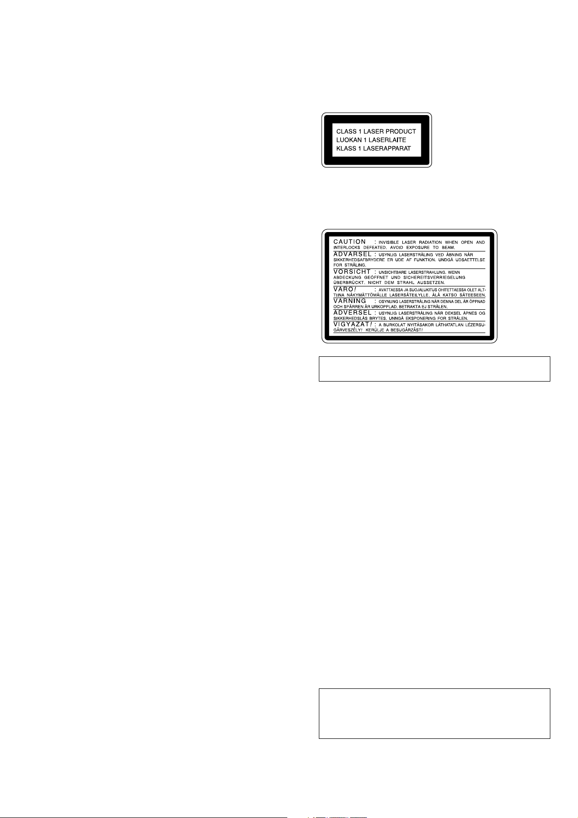
TABLE OF CONTENTS
1. GENERAL ...................................................................... 4
2. DISASSEMBLY............................................................. 7
3. SERVICE MODE .......................................................... 11
4. MECHANICAL ADJUSTMENTS............................ 15
5. ELECTRICAL ADJUSTMENTS ............................. 15
6. DIAGRAMS
6-1. Circuit Boards Location ·············································· 20
6-2. Block Diagrams ···························································21
6-3. Schematic Diagram Video Board (1/2) ···················25
6-4. Schematic Diagram Video Board (2/2) ···················26
6-5. Printed Wiring Board Video Board ························· 27
6-6. Printed Wiring Board BD Board ····························· 28
6-7. Schematic Diagam BD Board ·································29
6-8. Printed Wiring Baord CD Motor Section ················30
6-9. Schematic Diagram CD Motor Section ···················31
6-10.Printed Wiring Board Audio Board ·························32
6-11.Schematic Diagram Audio Board···························· 33
6-12.Printed W iring Board Leaf SW Board ···················· 34
6-13.Schematic Diagram Leaf SW Board ······················· 34
6-14.Printed Wiring Board Main Board ·························· 35
6-15.Schematic Diagram Main Board (1/3) ···················· 36
6-16.Schematic Diagram Main Board (2/3) ···················· 37
6-17.Schematic Diagram Main Board (3/3) ···················· 38
6-18.Printed Wiring Board Panel FL Board ···················· 40
6-19.Schematic Diagram Panel FL Board ·······················41
6-20.Printed Wiring Board Panel VR Board···················· 42
6-21.Schematic Diagram Panel VR Board ······················ 43
6-22.Printed Wiring Board
TC-A/TC-B/CD-L/CD-L2/CD-R/CD-R2 Boards ·······44
6-23.Schematic Diagram
TC-A/TC-B/CD-L/CD-L2/CD-R/CD-R2 Boards ·······45
6-24.Printed Wiring Board
Front Input/Headphone/MIC Boards··························· 46
6-25.Schematic Diagram
Front Input/Headphone/MIC Boards··························· 47
6-26.Printed Wiring Board PA Board······························ 48
6-27.Schematic Diagram PA Board ································· 49
7-28.Printed Wiring Board Surround Board ····················50
6-29.Schematic Diagram Surround Board······················· 51
6-30.Printed W iring Board Trans/Sub Trans Boards ······· 52
6-31.Schematic Diagram Trans/Sub Ttrans Boards········· 53
6-32.IC Block Diagrams ······················································ 54
6-33.IC Pin Function Description········································ 56
This appliance is classified as a CLASS 1 LASER product.
The CLASS 1 LASER PRODUCT MARKING is located on
the rear exterior.
Laser component in this product is capable of emitting radiation
exceeding the limit for Class 1.
The following caution label is located inside the unit.
NOTES ON HANDLING THE OPTICAL PICK-UP
BLOCK OR BASE UNIT
The laser diode in the optical pick-up block may suffer electrostatic
break-down because of the potential difference generated by the
charged electrostatic load, etc. on clothing and the human body.
During repair, pay attention to electrostatic break-down and also
use the procedure in the printed matter which is included in the
repair parts.
The flexible board is easily damaged and should be handled with
care.
NOTES ON LASER DIODE EMISSION CHECK
The laser beam on this model is concentrated so as to be focused on
the disc reflective surface by the objective lens in the optical pickup block. Therefore, when checking the laser diode emission,
observe from more than 30 cm away from the objective lens.
Notes on chip component replacement
• Never reuse a disconnected chip component.
• Notice that the minus side of a tantalum capacitor may be dam-
aged by heat.
7. EXPLODED VIEWS ................................................... 64
8. ELECTRICAL PARTS LIST ................................... 72
Flexible Circuit Board Repairing
• Keep the temperature of the soldering iron around 270 ˚C during repairing.
• Do not touch the soldering iron on the same conductor of the
circuit board (within 3 times).
• Be careful not to apply force on the conductor when soldering
or unsoldering.
CAUTION
Use of controls or adjustments or performance of procedures
other than those specified herein may result in hazardous
radiation exposure.
3
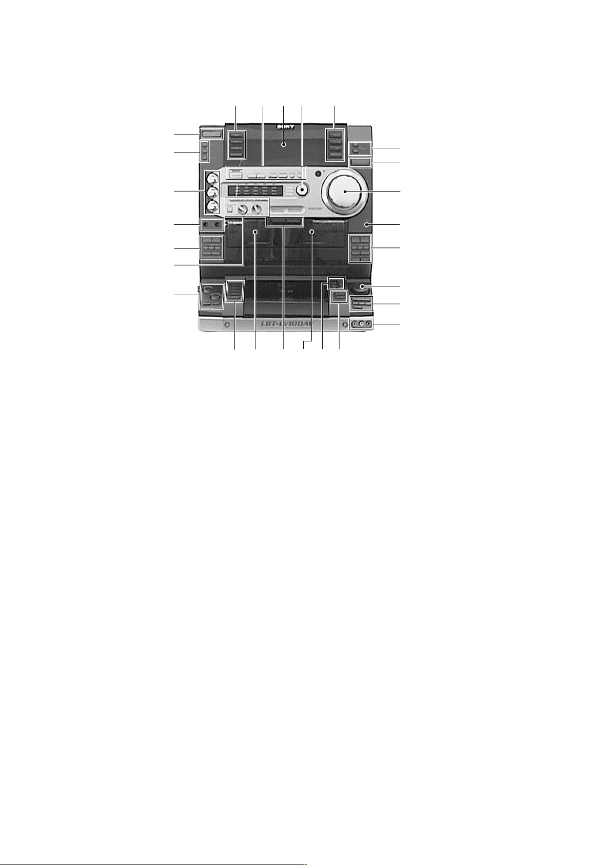
LOCATION OF CONTROLS
– Front Panel –
1
wh
SECTION 1
GENERAL
2
3
4
5
6
7
8
wg
wf
wd
ws
wa
1 ?/1 (POWER) button
2 DAILY button
REC button
SLEEP button
c/CLOCK SET button
3 TUNER/BAND button
TUNING +/– button
ENTER/NEXT button
TUNER MEMORY button
STEREO/MONO button
TUNING MODE button
PTY button
4 Display
5 v/B/V/b button
6 SYNC EQ button
SYNC BASS button
SURROUND button
MIX GUITAR/KARAOKE button
7 KEY CONTROL #/2 button
8 FUNCTION button
9 VOLUME control
0 PHONES jack
qa DECK B operating button
g button G button x button
m button M button X button
z REC button HI SPEED DUB button
CD SYNC button
qs . AMS > contr ol
qd CD operating button
G X button x button m button
M button DISC SKIP button
qf VIDEO 2 INPUT jack
w;
9
0
qa
qs
qd
qf
qh
qgqjqkql
qg PLAY MODE button
REPEAT button
qh ACTIVE button
SELECT button
RETURN button
PREV button
NEXT button
qj DECK B
qk Z A EJECT
Z B EJECT
ql DECK A
w; DISC1-5 button
wa LOOP button
FLASH button
NON-STOP button
EDIT button
ws SUPPER WOOFER MODE button
MIC LEVEL control
GUITAR LEVEL contro
wd DECK A operating button
g button G button x button
m button M button
DIRECTION button
DOLBY NR button
wf MIC MIX jack
GUITAR jackl
wg EFFECT button
GROOVE button
SUPER WOOFER button
wh POWER SAVE/DEMO (STAND BY) button
DISPLAY button
SPECTRUM AN ALYZER button
4
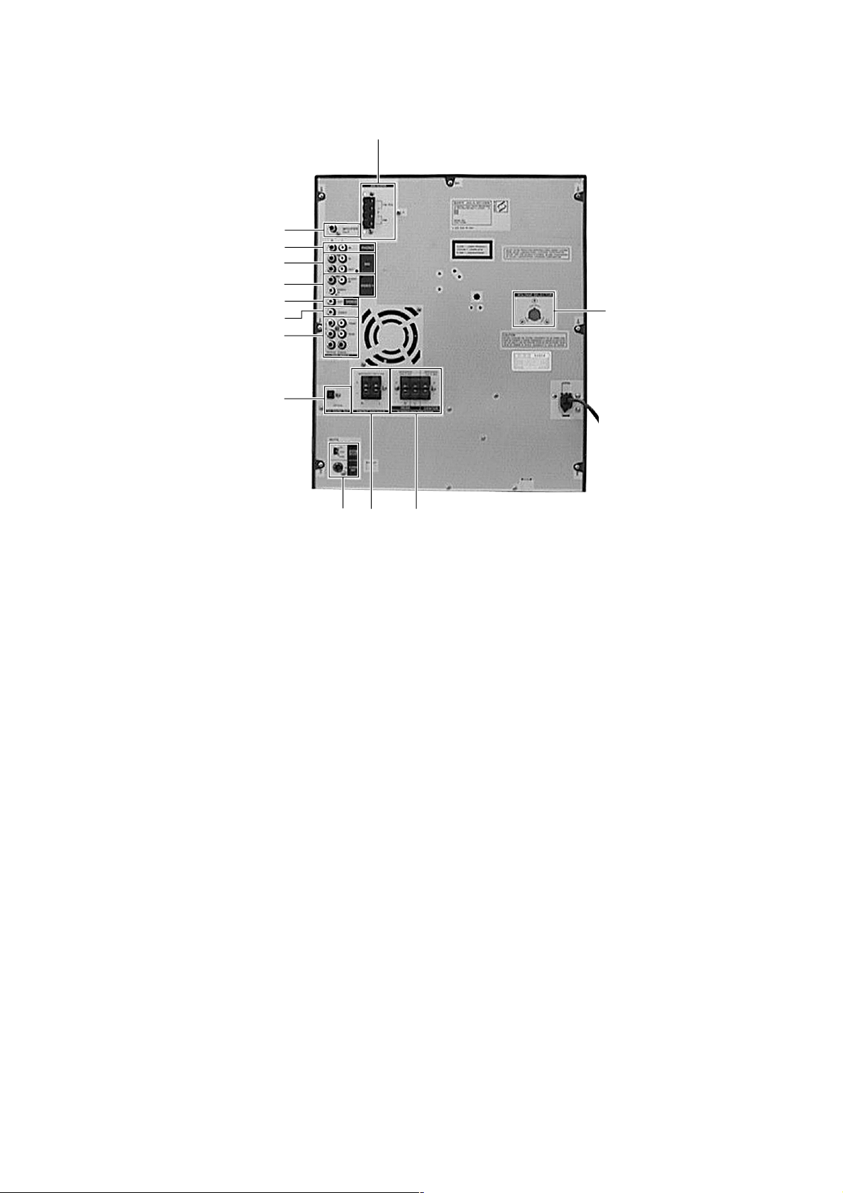
– Rear Panel –
qd
qs
qa
q;
9
8
7
6
1
2
45
1 ANTENNA terminal
2 VOLTAGE SELECTOR
3 SURROUND SPEAKER terminal
4 FRONT SPEAKER terminal
5 NOTE ONLY FOR VCD
6 CD DIGITAL OUT terminal
7 DVD INPUT FRONT jack
8 DVD INPUT VIDEL jack
9 VIDEO OUT jack
0 VIDEO 1 jack
qa MD IN/OUT jack
qs PHONO IN jack
qd WOOFER OUT jack
3
SYSTEM SELECT switch
S VIDEO OUT terminal
DVD INPUT REAR jack
DVD INPUT WOOFER jack
DVD INPUT CENTER jack
5
This section is extracted
from instruction manual.
6
SECTION 2
)
DISASSEMBLY
Note: Follow the disassembly procedure in the numerical order given.
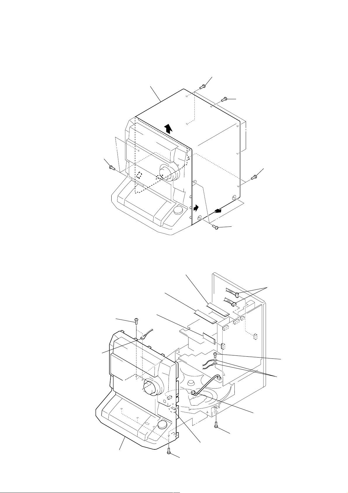
3-1. UPPER CASE
1 Three screws
(CASE3 TP2)
6 Upper case
(Remove in the direction of the arrows)
5 Four screws
(BVTT 3 × 6)
4 Screws
(BVTP3 × 8)
3 Two screws
(BVTP3 × 8
2 Three screws
(CASE3 TP2)
3-2. FRONT PANEL SECTION
7
Two screws
(BVTP3 × 8)
Lug
3
Wire (flat type)
(17 core) (CN304)
4
Wire (flat type)
(13 core) (CN431)
2
Wire (flat type)
(15 core) (CN303)
1
Two connectors
(CN452, 702)
Screw
6
(BVTP3 × 8)
Two lugs
Connector
5
(CN802)
0
Front panel section
(Be careful in has claws)
9
Four screws
(BVTP3 × 8)
Claw
8
Screw (BVTP3 × 8)
7
3-3. TAPE MECHANISM DECK (TCM-230PWR12)
Two screws
1
(BVTP3 × 8)
Two screws
2
(BVTP3 × 8)
Tape mechanism deck
3
(TCM-230PWR12)
3-4. MAIN BOARD
9
Wire (flat type)
(13 core) (CN411)
8
Connector
(CN102)
5
Eleven screws
(BVTP3 × 8)
7
Connector
(CN701)
1
Wire (flat type) (13 core) (CN441)
6
Back panel
2
(CN903)
qd
Main board
4
Five screws
(BVTP3 × 8)
3
Two screws
(BVTP3 × 8)
Connector
qa
Two screws
(BVTP3 × 8)
qs
q;
Connector
(CN412)
Two connector
(CN803, CN804)
8
3-5. CD MECHANISM DECK (CDM37L-5BD34L)
6
Three screws
(BVTP3 × 8)
1
Wire (flat type)
(13 core) (CN411)
9
2
Connector
(CN412)
8
Two screws
(BVTP3 × 8)
3
Open the cable clamp
7
Two screws
(BVTP3 × 8)
4
Connector
(CN301)
5
Two screws
(BVTP3 × 8)
CD mechanism dec
6
(CDM37L-5BD34L)
5
Five screws
(BVTP3 × 8)
k
1
Screw
(BVTP3 × 8)
3
Video board
2
Screw
(BVTP3 × 8)
4
Wire (flat type)
(23 core) (CN501)
9
3-6. BASE UNIT (BU-5BD34L)
3 Base unit
(BU-5BD34L)
2 Boss
1 BU fitting screw
3-7. DISC TABLE
Note: When the disc table is installed, adjust the positions of roller cam
and mark
table.
B
as shown in the figure, then set to the groove of disc
A
1 screw (BVTP3 × 8)
2 bracket (BU)
3 Step screw
4 Disc table
A
10

SECTION 3
SERVICE MODE
MC Cold Reset
• The cold reset clears all data including preset data stored in the RAM to initial conditions. Execute this mode when returning the set to
the customer.
Procedure:
1. Press three buttons c/CLOCK SET , ENTER , and ?/1 simultaneously.
2. “COLD RESET” is displayed on the fluorescent display tube and reset is executed.
CD Delivery Mode
• This mode moves the pick-up to the position durable to vibration. Use this mode when returning the set to the customer after repair.
Procedure:
1. Press ?/1 button to turn the set ON.
2. Press LOOP button and ?/1 button simultaneously.
3. A message “LOCK” is displayed on the fluorescent indicator tube, and the CD delivery mode is set.
MC Hot Reset
• This mode resets the set with the preset data kept stored in the memory. The hot reset mode functions same as if the power cord is
plugged in and out.
Procedure:
1. Press three buttons c/CLOCK SET , ENTER , and DISC 1 simultaneously.
2. The fluorescent indicator tube becomes blank instantaneously, and the set is reset.
Sled Servo Mode
• This mode can run the CD sled motor freely. Use this mode, for instance, when cleaning the pick-up.
Procedure:
1. Press ?/1 button to turn the set ON.
2. Press three buttons c/CLOCK SET , ENTER , and DISC 5 simultaneously.
3. The Sled Servo mode is selected, if “CD” is blanking on the fluorescent indicator tube.
4. With the CD in stop status, When the M botton is pressed, the optical pick-up moves outside. W hen m botton is pressed, it moves
inside.
5. To exit from this mode, perform as follows:
1) Move the pick-up to the most inside track.
2) Execute MC cold reset. (Press the three buttons c/CLOCK SET , ENTER , and ?/1 button simultaneously.)
Note:
• Always move the pick-up to most inside track when exiting from this mode. Otherwise, a disc will not be unloaded.
• Do not run the sled motor excessively, otherwise the gear can be chipped.
Change-over of AM Tuner Step between 9kHz and 10kHz (DR8AV Only)
• A step of AM channels can be changed over between 9kHz and 10kHz.
Procedure:
1. Press ?/1 button to turn the set ON.
2. Select the function “TUNER”, and press TUNER/BAND button to select the BAND “AM”.
3. Press ?/1 button to turn the set OFF.
4. Press ENTER and ?/1 buttons simultaneously, and the display of fluorescent indicator tube changes to “AM 9k STEP” or “AM 10k
STEP”, and thus the channel step is changed over.
LED and Fluorescent Indicator Tube All Lit, Key Check Mode
Procedure:
1. Press three buttons c/CLOCK SET , ENTER , and DISC 2 simultaneously.
2. LEDs and fluorescent indicator tube are all turned on.
Press DISC 2 button, and the key check mode is activated.
3. In the key check mode, the fluorescent indicator tube displays “K @ V0 J0”. Each time a button is pressed, “K”value increases.
However, once a button is pressed, it is no longer taken into account.
“J” Value increases like 1, 2, 3 ... if rotating . AMS > knob in “+” direction, or it decreases like 0, 9, 8 ... if rotating in “-”
direction.
“V” Value increases like 1, 2, 3 ... if rotating V OLUME knob in “+” direction, or it decreases like 0, 9, 8 ... if rotating in “-” direction.
4. To exit from this mode, press three buttons in the same manner as step 1, or disconnect the power cord.
11

AMS Test Mode
• This mode is used for checking the AMS operations of the tape deck.
JIG
7-819-039-12 Alignment tape, AMS-110A
Procedure:
1. Press the ?/1 button to turn the set ON.
2. Set the tape (AMS-110A).
3. Press the three buttons c/CLOCK SET , ENTER , and DISC 3 button simultaneously.
4. “TEST MODE” is displayed on the fluorescent display tube.
5. Press the FUNCTION button and switch the function to the deck with the tape (AMS-110A).
6. Press the CD SYNCHRO button. “AMS CHECK” is displayed on the fluorescent display tube and the tape is rewound.
7. AMS starts in the normal direction. If the AMS count is 2 at shut down, proceed to step 8.
“NG” is displayed at other times, and the deck stops.
8. AMS starts in the opposite direction. If the AMS count is 2 at shut down again, “OK” is displayed.
“NG” is displayed at other times.
Aging Mode
During the aging mode, both the CD player and tape deck are executed together.
• If an error occurs:
Aging stops, and the error state is displayed on the fluorescent display tube.
• If no error occurs:
Aging is repeated.
Procedure:
1. Press the ?/1 button to turn the set ON.
2. Load 10 minute tapes with unbent rec-proof tabs in decks A and B.
3. Set CDs on the DISC 1 and DISC 4 tables.
4. Set the CD mode REPEAT to OFF and PLAY MODE to ALL DISCS.
(Press the PLAY MODE and REPEAT buttons to set these modes.)
5. Press the FUNCTION button to switch the function to “CD”.
6. Press the three buttons c/CLOCK SET , ENTER , and DISC 4 button simultaneously.
7. Aging starts.
8. To end aging, press the ?/1 button to turn the set OFF.
Aging Sequence:
Aging is performed in the following sequence.
• T ape Deck
1. The tape in deck A is rewound. “TAPE A AG-1” is displayed.
2. The FWD side of deck A is played for two minutes.
“T APE A AG-2” is displayed.
3. The tape in deck A is fast forwarded. “T APE A A G-3” is displayed. Fast forward is carried out for 20 seconds or to the tape end.
4. The RVS side of deck A is played for two minutes.
“T APE A AG-4” is displayed.
5. The tape in deck A is rewound. “TAPE A AG-5” is displayed.
6. The FWD side of deck B is played for two minutes.
“TAPE B AG-2” is displayed.
7. The tape in deck B is fast forwarded. “TAPE B AG-3” is displayed. Fast forward is carried out for 20 seconds or to the tape end.
8. The RVS side of deck B is played for two minutes.
“TAPE B AG-4” is displayed.
9. The tape in deck A is rewound. “TAPE A AG-5” is displayed.
10. Repeated from step 2.
• CD
1. The tray rotates.
2. DISC 1 is chucked.
3. The TOC is read.
4. The first track is played for 2 seconds.
5. The last track is played for 2 seconds.
6. The tray rotates.
7. DISC 4 is chucked.
8. The TOC is read.
9. The first track is played for 2 seconds.
10. The last track is played for 2 seconds.
11. Repeated from step 1.
12

• Display when ended abnormally
When the tape deck is abnormal:
The state when ended abnormally is displayed.
The contents of display are the same as that during aging.
When the CD player is abnormal:
A message indicating that errors such as “CD MEC ERR” have occurred.
Check the error contents in the following error history display mode.
Error History Display Mode
Mode which enables the history of error occurring in the CD player to be checked.
Execute this mode after ending the aging mode.
Procedure:
1. Press the ?/1 button to turn the set ON.
2. Press the three buttons c/CLOCK SET , ENTER , and CD SYNCHRO simultaneously.
3. A message such as “EMC@@EDC**” is displayed.
@@ : Number of mechanical errors (Up to three past errors)
** : Number of errors (NO DISC ERROR) which occurs after chucking (Up to three past errors)
4. When checking the history of mechanical errors, press the PLAY MODE button. When checking errors after chucking, press the
REPEAT button to switch the display.
5. Press the ?/1 button to end and turn the set OFF.
6. To erase the error history, perform COLD reset.
(Press the three buttons c/CLOCK SET , ENTER , and DISC 1 simultaneously.
• Viewing the mechanical error history display
(Switch the history by pressing the PLAY MODE button.)
Display
E@@M#*****
@@ : Error number. 00 is the newest.
# : Operating state of table
0 : Currently in the INITIAL mode
7 : Currently rotating to the right
8 : Currently rotating to the left
A : Currently chucking down
B : Currently chucking up
* : Invalid
• Viewing the NO DISC ERROR history display
(Switch the history by pressing the REPEAT button.)
Display
E@@D##$$%*
@@ : Error number. 00 is the newest
## : Error contents
01: Focus error
02: GFS error
03: Setup error
$$ : Retries
00: NO DISC is determined without attempting chucking
retry
02: NO DISC is determined after chucking retry.
% : State when determined as NO DISC
1 : When stopped
2 : At setup
3 : At TOC READ
4 : When accessing
5 : When playing
6 : When pausing
7 : When manual searching (during play)
8 : When manual searching (during pausing)
* : Invalid
13
[VIDEO CD Color-bars Mode]
On this mode, the data of the color-bars signal as a picture signal
and the 1 kHz sine wave signal as a sound signal are output by the
mechanism controller (IC502) for the video CD signal check. When
measurement of the voltage and waveform on the VIDEO board,
perform it in this mode.
For reference, the color-bars signal can be observed at J302 (VIDEO
OUT) and the sound signal can be observed at J101 (VIDEO/MD
(AUDIO) OUT) using an oscilloscope.
Procedure:
1. Short the both ends of the land of SL503 of the VIDEO board.
2. Turn the po wer on. Press the [FUNCTION] button to select CD.
3. The color-bars appears when the CD is in stop status, and it
disappears when the CD goes in play status.
4. After measuring, remove the lead wire connected.
– VIDEO board (Side A) –
D502
SL503
CN503
SL502
SL503
SL502
SL501
IC505
IC502
SL501
CN501
14
SECTION 4
MECHANICAL ADJUSTMENTS
SECTION 5
ELECTRICAL ADJUSTMENTS
Precaution
1. Clean the following par ts with a denatured alcohol-moistened
swab:
record/playback heads pinch rollers
erase head rubber belts
capstan idlers
2. Demagnetize the record/playback head with a head
demagnetizer.
3. Do not use a magnetized screwdriver for the adjustments.
4. After the adjustments, apply suitable locking compound to the
parts adjusted.
5. The adjustments should be performed with the rated power
supply voltage unless otherwise noted.
Torque Measurement
Mode Torque meter
Meter reading
3.06 N • m to 6.96 N • m
FWD
CQ-102C
31 to 71 g • cm
(0.43 – 0.98 oz • inch)
FWD
back tension
CQ-102C
0.19 N • m to 0.58 N • m
2 to 6 g • cm
(0.02 – 0.08 oz • inch)
3.06 N • m to 6.96 N • m
REV
CQ-102RC
31 to 71 g • cm
(0.43 – 0.98 oz • inch)
REV
back tension
CQ-102RC
0.19 N • m to 0.58 N • m
2 to 6 g • cm
(0.02 – 0.08 oz • inch)
6.96 N • m to 14.02 N • m
FF/REW
CQ-201B
71 to 143 g • cm
(0.98 – 1.99 oz • inch)
9.80 N • m
FWD tension
CQ-403A
100 g or more
(3.53 oz or more)
9.80 N • m
REV tension
CQ-403R
100 g or more
(3.53 oz or more)
DECK SECTION 0 dB=0.775V
1. Demagnetize the record/playback head with a head
demagnetizer.
2. Do not use a magnetized screwdriver for the adjustments.
3. After the adjustments, apply suitable locking compound to the
parts adjusted.
4. The adjustments should be performed with the rated power
supply voltage unless otherwise noted.
5. The adjustments should be performed in the order giv en in this
service manual. (As a general rule, playback circuit adjustment
should be completed before performing recording circuit
adjustment.)
6. The adjustments should be performed for both L-CH and RCH.
7. Switches and controls should be set as follows unless otherwise
specified.
Tape Signal Used for
P-4-A100
WS-48B
P-4-L300
Record/Playback Head Azimuth Adjustment
(Deck A, Deck B)
Note: Perform this adjustments for both decks.
Procedure:
1. Mode : Playback
test tape
P-4-A100
(10kHz, –10dB)
2. T urn the adjustment screw and check output peaks. If the peaks
do not match for L-CH and R-CH, turn the adjustment screw
so that outputs match within 1 dB of peak.
10 kHz, –10 dB
3 kHz, 0 dB
315 Hz, 0 dB
MD OUT
set
Azimuth Adjustment
Tape Speed Adjustment
Level Adjustment
level meter
+
–
L-CH
peak
screw
position
R-CH
peak
output
level
within
1 dB
L-CH
peak
R-CH
peak
within 1dB
screw
position
15
3. Mode: Playback Tape Speed Adjustment (Deck A)
)
test tape
P-4-A100
(10kHz, –10dB)
oscilloscope
MD OUT
Note: Set the test mode using the following method and begin tape
speed adjustment.
In the test mode, the speed will switch to double speed or
normal speed each time the HI-SPEED DUB button is pressed.
set
Waveform of oscilloscope
in phase 45°
good
90°
135°
180°
wrong
4. After the adjustments, apply suitable locking compound to the
parts adjusted.
Adjustment Location: Playback Head (Deck A)
Record/Playback/Erase Head (Deck B)
Procedure:
With the power turned ON, press the c/CLOCK SET button,
ENTER button, and DISC 3 button simultaneously.
(The “VOLUME” on the fluorescent display tube will blink while
in the test mode.)
To exit the test mode, press the ?/1 button.
1. Insert the WS-48B into deck B.
2. Press the H button of deck B.
3. Press the HI-SPEED DUB button and play the tape at double speed.
4. Adjust RV1001 of the LEAF SW board so that the reading of
the frequency counter becomes 6000 ± 180 Hz.
5. Press the HI-SPEED DUB button and play the tape at normal speed.
6. Adjust RV1002 of the LEAF SW board so that the reading of
the frequency counter becomes 3000 ± 90 Hz.
Adjustment Location: LEAF SW board
Sample Value of Wow and flutter
W.RMS (JIS) less than 0.3%
(test tape: WS-48B)
Playback Level Adjustment (Deck A, Deck B)
Procedure:
Mode: Playback
test tape
P-4-L300
(315Hz, 0dB)
set
MD OUT
level meter
Deck A is RV311 (L-CH) and RV411 (R-CH), deck B is RV301
(L-CH) and RV401 (R-CH)
so that adjustment within the following adjustment level.
Adjustment level:
CN301 playback level: 301.5 to 338.3 mV (–8.2 to –7.2 dB)
level difference between the channels: within ± 0.5 dB
Adjustment Location: AUDIO board
Adjustment Location
[LEAF SW BOARD]
RV1001(High Speed)
RV1002(Normal Speed
16
RV1002 RV1001
Record Bias Adjustment (Deck B)
AF OSC
VIDEO 1 (AUDIO) IN
315Hz 50 mV (–23.8 dB)
blank tape
CS-123
set
attenuator
600 Ω
Record Level (Lch)
RV301
RV351
Record Level (Rch)
IC301
56
43
42
29
28
15
14
1
1
3
Record Level Adjustment (Deck B)
Procedure:
INTRODUCTION
When set to the test mode performed in Tape Speed
Adjustment,
when the tape is rewound after recording, the “REC memory mode”
which rewinds only the recorded portion and playback is set.
This “REC memory mode” is convenient for performing this
adjustment. During recording, the input signal FUNCTION will
automatically switch to VIDEO 1.
(After recording, press the m button without stopping will
return to the position where recording was started.)
1. Press FUNCTION button to select VIDEO 1. (This step is not
necessary if the above test mode has already been set.)
2. Insert a tape into deck B, press the z REC button, and
then press the H button to start recording.
3. Mode: Record
4. Mode: Playback
5. Confirm playback the signal recorded in step 2 become
adjustment level as follows.
VIDEO 1 (AUDIO) IN
1) 315 Hz
2) 10 kHz
AF OSC
attenuator
600 Ω
} 50 mV (–23.8 dB)
blank tape
CS-123
set
Procedure:
INTRODUCTION
When set to the test mode performed in Tape Speed Adjustment
when the tape is rewound after recording, the “REC memory mode”
which rewinds only the recorded portion and playback is set.
This “REC memory mode” is convenient for performing this
adjustment. During recording, the input signal FUNCTION will
automatically switch to VIDEO 1.
(After recording, press the m button without stopping will
return to the position where recording was started.)
1. Press FUNCTION button to select VIDEO 1. (This step is not
necessary if the above test mode has already been set.)
2. Insert a tape into deck B, press the z REC button, and
then press the H button to start recording.
3. Mode: Record
4. Mode: Playback
5. Confirm playback the signal recorded in step 2 become
adjustment level as follows.
,
If these levels do not adjustment level, adjust the RV341 (LCH) and R V441 (R-CH) on the A UDIO board to repeat steps 3
and 4.
recorded
position
set
MD OUT
level meter
Adjustment level: The playback output of 10 kHz le vel dif ference
against 315 Hz reference should be ± 1.0 dB.
Adjustment Location: AUDIO board
Adjustment Location:
[AUDIO BOARD] (Conductor Side)
RV341(Lch),RV441(Rch)
Record Bias
RV311(Lch),RV411(Rch)
Playback Level (Deck A)
If these levels do not adjustment level, adjust the RV301 (LCH) and R V351 (R-CH) on the MAIN board to repeat steps 3
and 4.
recorded
position
set
MD OUT
level meter
Adjustment level:
CN403 playback level: 47.2 to 53.0 mV (–24.3 to –23.3 dB)
Adjustment Location: MAIN board
[MAIN BOARD] (Conductor Side)
RV301 RV401
RV441 RV341
RV301(Lch),RV401(Rch)
Playback Level (Deck B)
RV311
RV411
17
CD SECTION
e
e
V
+
–
BD board
TP (TE)
TP (VC)
oscilloscope
)
Note:
1. CD Block is basically designed to operate without adjustment. Therefore, check each item in order given.
2. Use YEDS-18 disc (3-702-101-01) unless otherwise indicated.
3. Use an oscilloscope with more than 10 MΩ impedance.
4. Clean the object lens by an applicator with neutral detergent when the
signal level is low than specified value with the following checks.
E-F Balance (1 Track Jump) Check
S-Curve Check
BD board
TP (FE)
TP (VC)
oscilloscop
+
–
Procedure:
1. Connect oscilloscope to TP (FE).
2. Connect between TP (FE1) and TP (VC) by lead wire.
3. Connect between TP (AGCCON) and TP (GND) by lead wire.
4. Turn the power ON.
5. Load a disc (YEDS-18) and actuate the focus search. (In
consequence of open and close the disc tray, actuate the focus
search)
6. Cofirm that the oscilloscope waveform (S-curve) is symmetrical
between A and B. And confirm peak to peak level within
4 ± 1 Vp-p.
S-curve waveform
symmetry
A
within 4 ± 1 Vp-p
B
7. After check, remove the lead wire connected in step 2 and 3.
Note: • Try to measure sev eral times to make sure than the ratio of A : B
or B : A is more than 10 : 7.
• Take sweep time as long as possible and light up the brightness
to obtain best waveform.
Procedure :
1. Connect oscilloscpe to TP (TE) and TP (VC).
2. Turn the power ON.
3. Load a disc (YEDS-18) and playback the number five track.
4. Press the ^ (CD) button. (Becomes the 1 track jump mode)
5. Confirm that the level B and A (DC v oltage) on the oscilloscope
waveform.
1 track jump waveform
B
0V
level = 1.3 ± 0.6 Vp-p symmetry
Specified level: × 100 = less than ± 22%
A
B
center of
waveform
A (DC voltage
6. After check, remove the lead wire connected in step 1.
Checking Location:
– BD BOARD (Side B) –
RF Level Check
oscilloscop
BD board
TP (RF)
TP (VC)
+
–
Procedure:
1. Connect oscilloscope to TP (RF).
2. Connect between TP (AGCCON) and TP (GND) by lead wire.
3. Turn the power ON.
4. Load a disc (YEDS-18) and press the ^ button to play.
5. Confirm that the oscilloscope waveform is clear and check RF
signal level is correct or not.
6. After check, remove the lead wire connected in step 2.
Note: Clear RF signal wa veform means that the shape “≈” can be clearly
distinguished at the center of the waveform.
VOLT/DIV: 200 m
TIME/DIV: 500 ns
level:
1.45 ± 0.3 Vp-p
TP (AGCCON)
TP (RF)
IC102
TP (TE)
TP (FE)
IC103
TP (VC)
TP (GND)
TP (FE1)
IC101
18

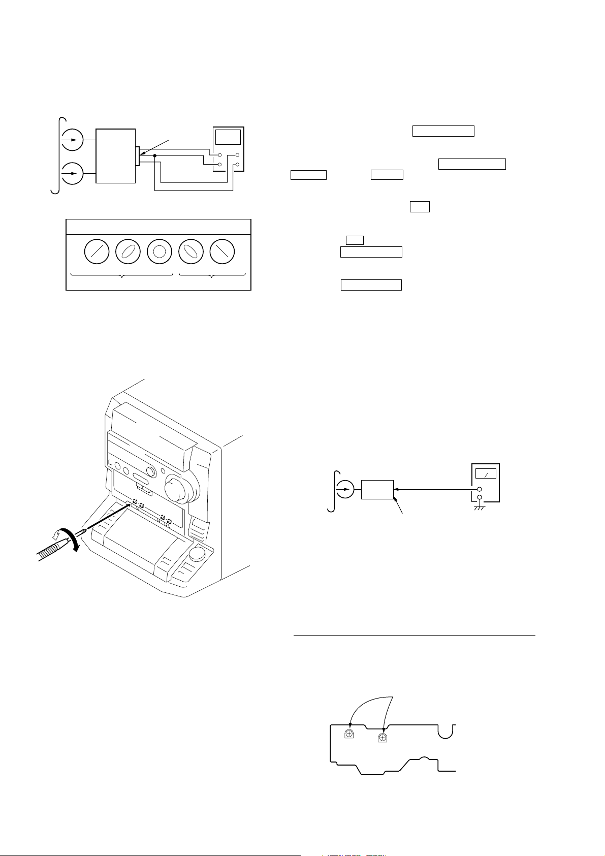
VIDEO SECTION
Frequency Adjustment
Connection:
VIDEO board
TP508 (27 MHz)
frequency counter
+
–
Procedure:
1. Connect the frequency counter to TP508 (27 MHz) on VIDEO
board.
2. Turned power switch on.
3. Press the [FUNCTION] button to select the CD.
4. Adjust CT503 on the VIDEO board so that the frequency counter
reading 27.0 MHz ± 80 Hz at stop status.
Adjustment Location:
– VIDEO Board (Side A) –
IC507
IC505
TP508
(27 MHz)
CT503
VIDEO
Frequency
Adjustment
1919
SECTION 6
d
DIAGRAMS
NOTE FOR PRINTED WIRING BOARDS AND SCHEMATIC DIAGRAMS
(In addition to this, the necessary note is printed in each block)
Note on Printed Wiring Board:
• X : parts extracted from the component side.
f
•
• b : Pattern from the side which enables seeing.
Caution:
Pattern face side: Parts on the pattern face side seen from
(Side B) the pattern face are indicated.
Parts face side: Parts on the parts face side seen from
(Side A) the parts face are indicated.
• Indication of transisitor.
: internal component.
Q
B
CE
These are omitted.
Q
B
CE
These are omitted.
C
Q
B
E
These are omitted.
Note on Schematic Diagram:
• All capacitors are in µF unless otherwise noted. pF: µµF
50 WV or less are not indicated except for electrolytics
and tantalums.
• All resistors are in Ω and 1/
specified.
f
•
• 2 : nonflammable resistor.
• 5 : fusible resistor.
• C : panel designation.
The components identified by mark 0 or dotted
line with mark 0 are critical for safety.
Replace only with part number specified.
• U : B+ Line.
• V : B– Line.
• H : adjustment for repair.
• Voltages are tak en with a VOM (Input impedance 10 MΩ).
• Waveforms are taken with a oscilloscope.
• Circled numbers refer to waveforms.
• Signal path.
• Abbreviation
: internal component.
Voltage variations may be noted due to normal production tolerances.
Voltage variations may be noted due to normal production tolerances.
F : TUNER (FM/AM)
E : PLAYBACK (DECK A)
d : PLAYBACK (DECK B)
G : RECORD
J : CD PLAY (ANALOG OUT)
c : CD PLAY (DIGITAL OUT)
N : MIC INPUT
EA : Saudi Arabia model.
SP : Singapore model.
MY : Malaysia model.
IA : Indonesian model.
4
W or less unless otherwise
6-1. CIRCUIT BOARDS LOCATION
TRANS board
PANEL FL board
MIC board
TC-A board
CD-L board
CD-L2 board
P ANEL VR board
LEAF SW board
CD-R board
TUNER UNIT (FM/AM)
TC-B board
CD-R2 board
FRONT INPUT board
TABLE SENSOR board
SURROUND AMP board
MAIN board
PA
board
VIDEO board
HEADPHONE boar
d
CD MOTOR board
AUDIO board
BD boar
LED board
2020
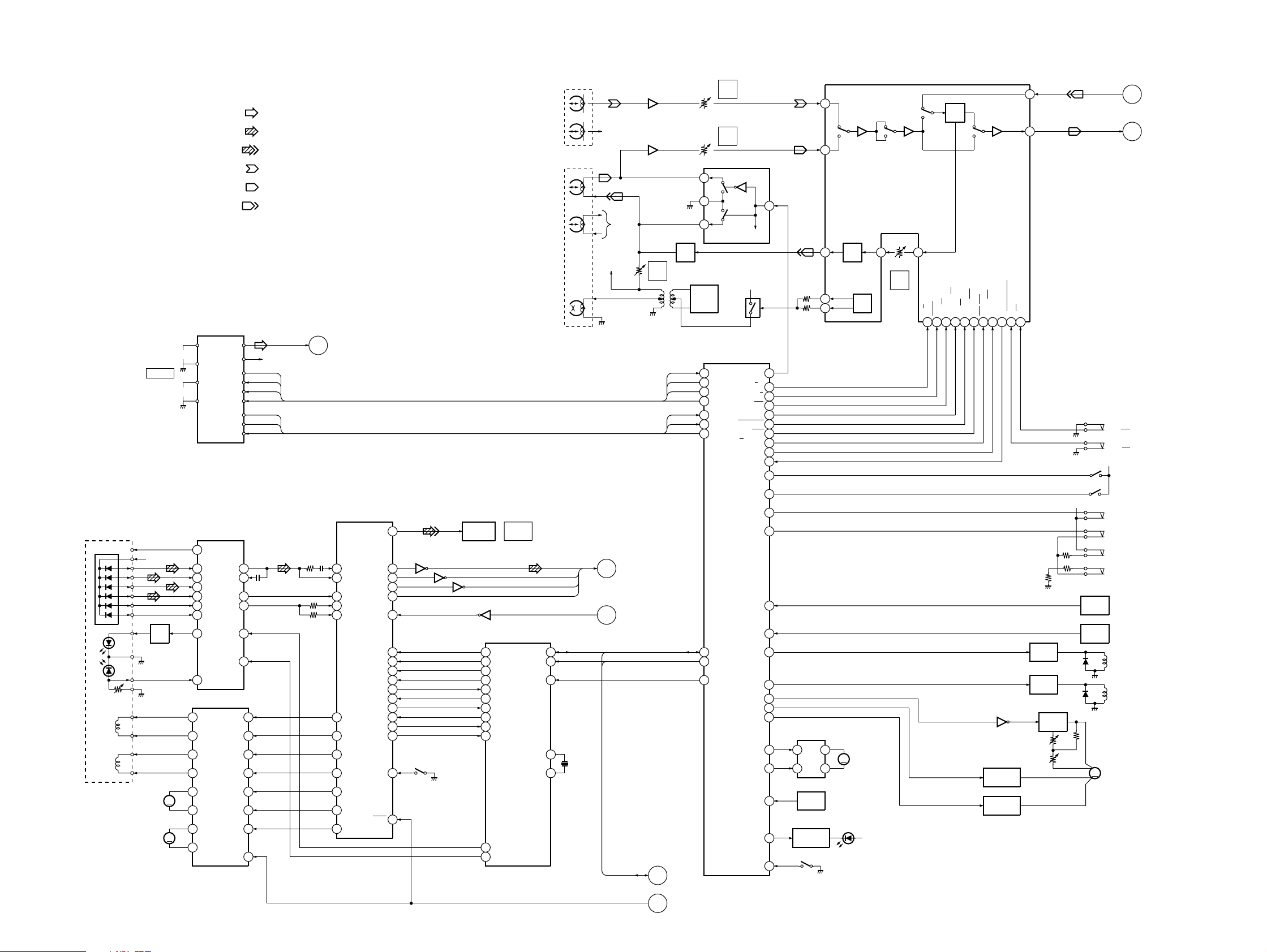
6-1. BLOCK DIAGRAMS TUNER/CD/DECK SECION
HCD-LV100AV
OPTICAL PICK-UP
BLOCK
(KSS-213D/QNP)
VC
A
B
C
D
E
F
LD
GND
PD
VR
FOCUS
COIL
TRACKING
COIL
16
R-CH
PB EQ
AMP
IC611
57
PB EQ
AMP
IC601
75
L331,C332
RV341
REC
BIAS
T621
BIAS
TRAP
RV311
RV301
1
2
3
BIAS
OSC
Q621,622
PB(L)
LEVEL
PB(L)
LEVEL
REC/PB SWITCH
IC602
+7V
Q623
R CH
REC
PB
B NORM/CROM/METAL
LM ON/OFF
MS OUT
26
17
19
43
40
A120/70
48
A
B
46
DECK A/B SELECT
PB/REC EQ AMP
4
REC
36
EQ
NORM
33
32
CROM
BIAS
SW
70
120
IC301
38
RV301
REC(L)
LEVEL
REC
DOLBY
PB A/B
16
NORM/HIGH
ALC ON/OFF
15
18
B
DOL
PAS
BIAS ON/OFF
RM ON/OFF
20
22
NR ON/OFF
23
24
REC /PB/PASS
25
PB
39
TC REC-L
TC PB-L
MAIN
SECTION
F
(Page 22)
MAIN
SECTION
G
(Page 22)
• RCH is omitted
• Signal Path
: FM
: CD
: DIGITAL OUT
: PB (DECK A)
: PB (DECK B)
: REC (DECK B)
HP101
HEAD
HRPE101
REC/PB
HEAD
ERASE
HEAD
DECK-A
PB
R-CH
DECK-B
R-CH
TUNER UNIT
FM 75Ω
ANTENNA
AM
+5V
Q101
LD
DRIVE
F-
F+
T-
T+
M101
SPINDLE
MOTOR
M102
SLED
MOTOR
12
11
10
13
14
11
12
18
M
17
16
M
15
ST-L
ST-R
ST DOUT
ST DIN
ST CLK
STCE
TUNED
STEREO
MUTE
RF AMP
IC103
VC
RFO
A
5
6
7
8
3
4
RFI
B
C
FE
D
TE
E
F
LD
PD
IC102
MOTOR/COIL DRIVE
CH1RI
CH1RO
CH1FI
CH1FO
CH2RI
CH2RO
CH2FI
CH2FO
CH3RI
CH3RO
CH3FO
CH4RO
CH4FO
MUTE
ST MUTE
16
17
14
13
22LD ON
21HOLD SW
3
2
6
5
23
24CH3FI
25CH4INS
20
ST-L
R-CH
DO
DI
CL
CE
TUNED
STEREO
MAIN
A
SECTION
(Page 22)
DIGITAL SIGNAL PROC.
50
43
39
41
40
34
33
32
31
30
29
25
DIGITAL SERVO
D/A CONV.
IC101
RFAC
RFDC
FE
TE
SE
FRDR
FFDR
TRDR
TFDR
SRDR
SFDR
MDP
D OUT
PCMD
BCLK
LRCK
C2PO
XTAI
DATA
CLOK
XLAT
MUTE
SQSO
SQCK
SENS
SCLK
SCOR
XTSL
SSTP
XRST
64
66
67
65
14
71
4
6
5
3
76
77
7
8
15
69
27
2
LEVEL SHIFT
IC501
14
13 10
IC781
DIGTAL OUT
58
S101
LIMIT
IN SW
4
CD
IC104
2
CD MECHA CONT
DSP DATA
3
DSP CLK
5
DSP LATH
4
DSP MUTE
10
SUBQ DATA
36
SUBQ CLK
37
SENSE
1
SENSE CLK
2
SCOR
18
CTRL1
11
28
LDON
27
CTRL2
DIGITAL
OUT
OPTICAL
IC502(1/2)
IIC DATA
IIC CLK
XRESET
XOUT
SYSTEM CONTROL
54
53
55
52
51
50
49
30
29
59
ST DIN
ST DOUT
ST CLK
ST CE
TUNED
STEREO
ST MUTE
IIC DATA
IIC CLK
XRST
IC501(1/3)
REC MUTE
NR ON/OFF
R/PB PAS
TC MUTE
CAP M H/L 76
CAP M CONT2
CAP M CONT1
DISC LED
ENC3/UP SW
PB A/B
EQ H/N
ALC
BIAS
AMS IN
A PLAY
B PLAY
A HALF
B HALF
A SHUT
B SHUT
A TRIG
B TRIG
TBL-R
100TC RELAY
84
83
85
82
81
80
79
78
77
87
86
88
89
91
90
73
72
74
75
IC201
9
63TBL-L
65
61T SENS
69
68
MOTOR
DRIVE
1
IC202
DISC
SENSOR
LED DRIVE
Q201
7
3
UP SW
S201
M
D201
DISC
M201
TURN
MOTOR
Q335
Q336-339
CAP MOTOR
SPEED CONT
Q340-343
CAP MOTOR
DRIVE
Q333,334
A TRIG
DRIVE
Q331,332
B TRIG
DRIVE
RV1002
NORM S
RV1001
HIGH S
Q1001
MOTOR
CONT
+5V
IC1001
A REEL
DET
IC1002
B REEL
DET
M
+5V
A TRG M+
B TRG M+
M901
CAPSTAN
MOTOR
S1004
A 120/70
S1008
B 120/70
S1001
A PLAY
S1002
B PLAY
S1003
A HALF
S1006
B HALF
S1005
REC A
S1009
REC B
DO
DI
CL
CE
TUNED
STEREO
ST MUTE
CD DATA
CD BCK
CD LRCK
C2PO
XTAL33.8M
30
29
12
XIN
15
X501
10MHz
13
B
C
VIDEO
SECTION
(Page 23)
VIDEO
SECTION
(Page 23)
IIC DATA
IIC CLK
XRST
D
E
DISPLAY
SECTION
(Page 24)
VIDEO
SECTION
(Page 23)
2121
HCD-LV100AV
MAIN SECTION
VIDEO 2
INPUT
DVD
INPUT
PHONO IN
VIDEO 1 IN
(AUDIO)
MD IN
MD OUT
AUDIO
VIDEO
CENTER
WOOFER
VIDEO 1 IN
(VIDEO)
VIDEO
OUT
DVD
VIDEO IN
TUNER
SECTION
(Page 21)
VIDEO
SECTION
(Page 23)
TC
SECTION
(Page 21)
TC
SECTION
(Page 21)
FRONT
REAR
VIDEO
SECTION
(Page 23)
R CH
MUTE
Q805
R CH
R CH
M901
FAN
TM401
L
R
L
R
TM402
L
R
L
R
L
R
J704
SPA SIG
MIC SIG
TA MUTE
• RCH is omitted
• Signal Path
: FM
: CD
: PB (DECK A)
: PB (DECK B)
: REC (DECK B)
: VIDEO
HP IN
FAN DRIVE
Q961,962
INPUT SELECT/
GRAPHIC EQ CONT/
ELECTRICAL VOLUME
ST-L
A
CD-L
I
TC REC-L
F
TC PB-L
G
V L-CH
PHONO AMP
IC601
31
VIDEO SELECT
6
1
10
4
8
IC191
IN3
IN1
VD OUT
IN2
IN4
12
14
15
11
A
2
B
3
C
5
16
AUDIO SELECT
IC181
10
9
A
B
A
B
AB
28
46
V MUTE
FUNC SEL045FUNC SEL1
DATA
CLOCK
LATCH
13
DOLBY
SURROUND PROCESSOR
IC201
1
L IN
80
VR SW IN
DATA
24
PL DATA
DATA
CLK
LAT
CLK
23
LAT
25
PL CLK
74
77
76
79
22
23
24
PL LAT
LT IN
SL IN
C IN
SW IN
DATA
SCK
REQ
SL OUT
C OUT
SW OUT
9
3
17
47
DATA
DATA
CLOCK
48
CLK
LATCH
38
LAT
J701
L
L
L
L
J804
L
J703
J702
H
68
66
58
67
69
65
57
64
60
72
59
33
32
34
IC101
INB2
IND2
RECA2
INC2
INA2
INE2
RECB2
INF2
KEYIN2
SW
KYE OUT2
DATA
CLOCK
LATCH
OUT2
BB A2
BB B2
36
37IN2
39
38
30L+R
2MIC IN
6
LINE MUTE
Q115
MUTE CONT
Q803
34
SW MODE
MUTE
Q113
Q111
SYSTEM CONTROL
IC501(2/3)
DBFB CONT
Q112
7
27
DBFB H/L
PROTECT
POWER AMP
IC901
18
17
PROTRCT
Q432
Q437,439
RELAY
+B SW
Q431
10
MUTE
Q281
MUTE
Q271
11
22
OVER LOAD
DETECT
RELAY +B
Q801
D803
D401
93
HP MUTE
R-CH
DC DET
Q433,434
OVER HEAT
DETECT
Q831,832
MUTE CONT
Q833
32.768kHz
10
TH831
X501
XC IN
11
+7V
XC OUT
15
X502
16MHz
X IN
13
X OUT
3
F RELAY
RELAY
DRIVE
Q401,402
MUTE
Q103,104
RELAY
DRIVE
Q403,407
MUTE
CONT
4
REAR RELAY
SURROUND
IC101
10 5
OVER LOAD
DETECT
Q101,151
IC101
14 6
Q804
AMP
RY401
12
RY402
MUTE
Q731
D807
36
HEADPHONS
FRONT
SPEAKER
REAR SURROUND
CENTER
SPEAKER
WOOFER
OUT
DISPLAY
J
SECTION
(Page 24)
DISPLAY
K
SECTION
(Page 24)
POWER
L
SECTION
(Page 24)
J803
SPEAKER
2222
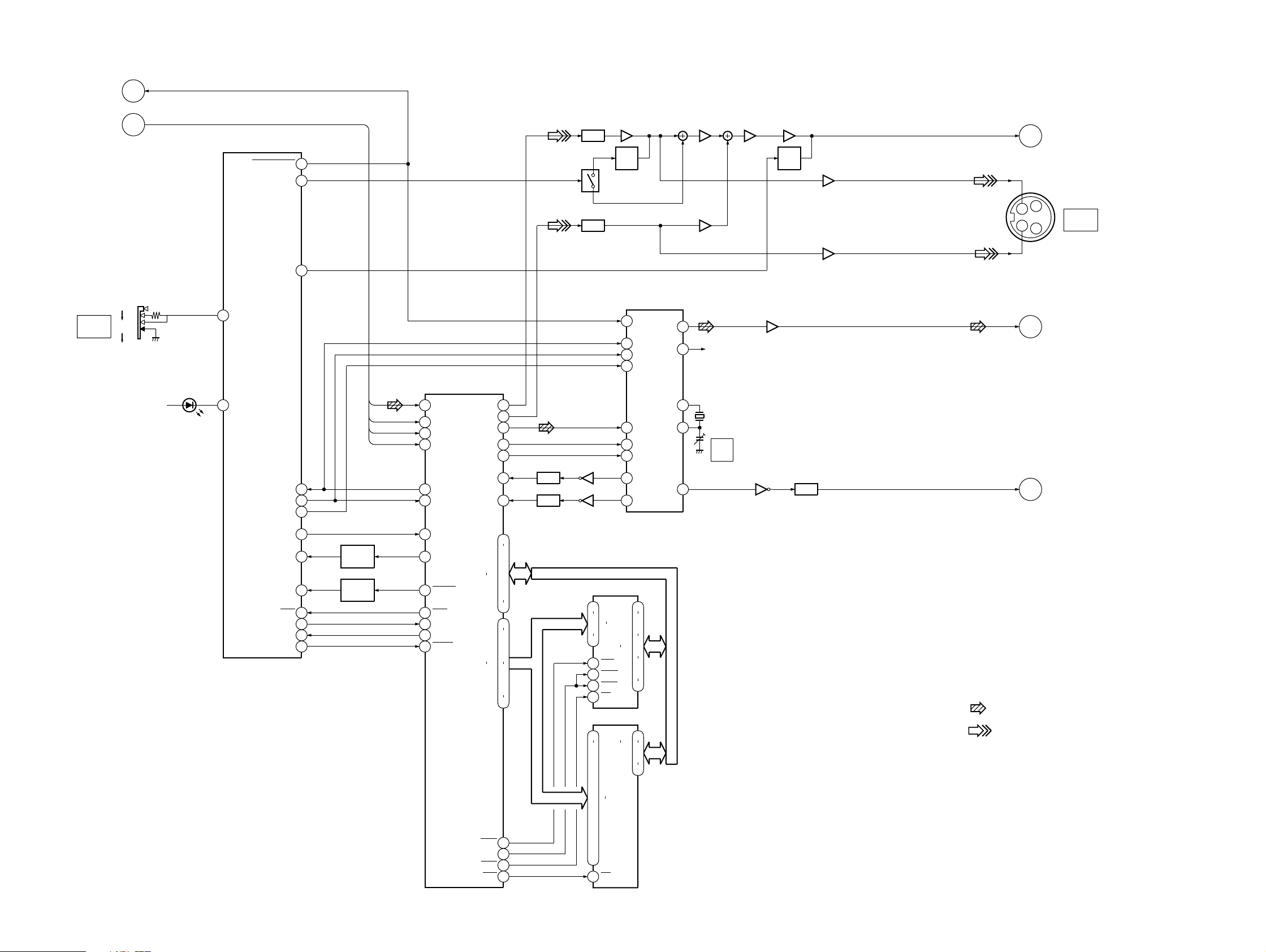
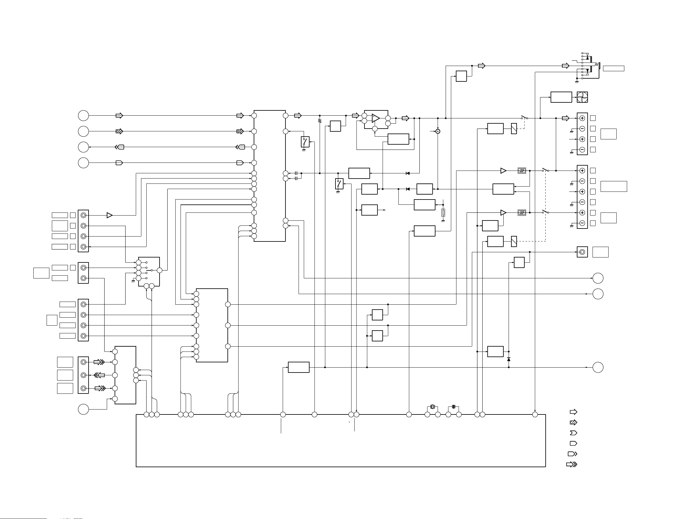
VIDEO CD SECTION
HCD-LV100AV
SECTION
(Page 21)
SECTION
(Page 21)
S501
SYSTEM
SELECT
CD
CD
NTSC
AUTO
PAL
XRST
E
CD DATA/CD BCK/CD LRCK/C2PO
B
SELF
DIAGNOSIS
D502
D+5V
93
73
16
CD MECHA CONT
IC502(2/2)
DEVICE RESET
SHARPNESS
NT/PAL
TEST LED
V MUTE
DATA1 I
DATA1 O
DF LATH
CLK1
HINT
HSEL
HRDY
RESET
Q307 Q308
B.P.F
FILTER
Q306
B.P.F
3
DRAM
IC507
16
A0
19
.
A8
22
DQ1
26
DQ16
14
RAS
28
UCAS
29
LCAS
13
WE
PROGRAM ROM
IC506
DQ1
12
DQ16
5
.
27
.
26
.
23
.
A0
25
.
A8
4
.
28
.
29
.
3
.
2
.
30
22
CE
Q302
DIGITAL FILTER
D/A CONV
10
RSTB
9
MD
8
MC
7
ML
18
DATA
17
BCK
19
LRCK
21
768FSO
4
MCKO
2
5
.
7
10
.
31
34
.
36
39
13
15
.
17
21
IC509
V OUT L
V OUT R
384FSO
XT1
XT2
Q304
14
11
1
27MHz
24
20
77
34
65
MPEG VIDEO/AUDIO DEC
VIDEO SIGNAL PROC
IC505
4
CD DATA
3
CD BCK
5
CD LRCK
6
CD C2PO
32
31
22
33
25H SYNC
45V SYNC
20
21
23
24
BUFFER
Q501
BUFFER
Q502
112
119
117
101
93
114
121
113
60
HD OUT
HD IN
HCK
H SYNC
V SYNC
HINT
HSEL
HRDY
RESET
Y OUT
C OUT
DA DATA
DA BCK
DA LRCK
DA XCLK
VCK
MD0
MD15
MA0
MA10
RAS0
CAS
69
75
110
111
108
86
106
10
15
.
17
.
19
.
21
.
23
29
58
56
.
54
.
52
50
.
48
.
46
44
42
40
38MWE
37MCE
L.P.F
L.P.F
IC504
811
6
IC504
27MHz
R-CH
X503
CT503
VIDEO
Q310
FRQ
IC401
5
MUTE
Q454
L.P.F
IC101
21
IC504
112
7
L.P.F
3
IC401
Q303
V L-CH
1
Y
C
CD-L
XTAL33.8M
• Signal Path
: CD
: VIDEO
MAIN
H
SECTION
(Page 22)
MAIN
SECTION
(Page 22)
CD
SECTION
(Page 21)
J301
S VIDEO
OUT
2
4
3
1
I
C
2323
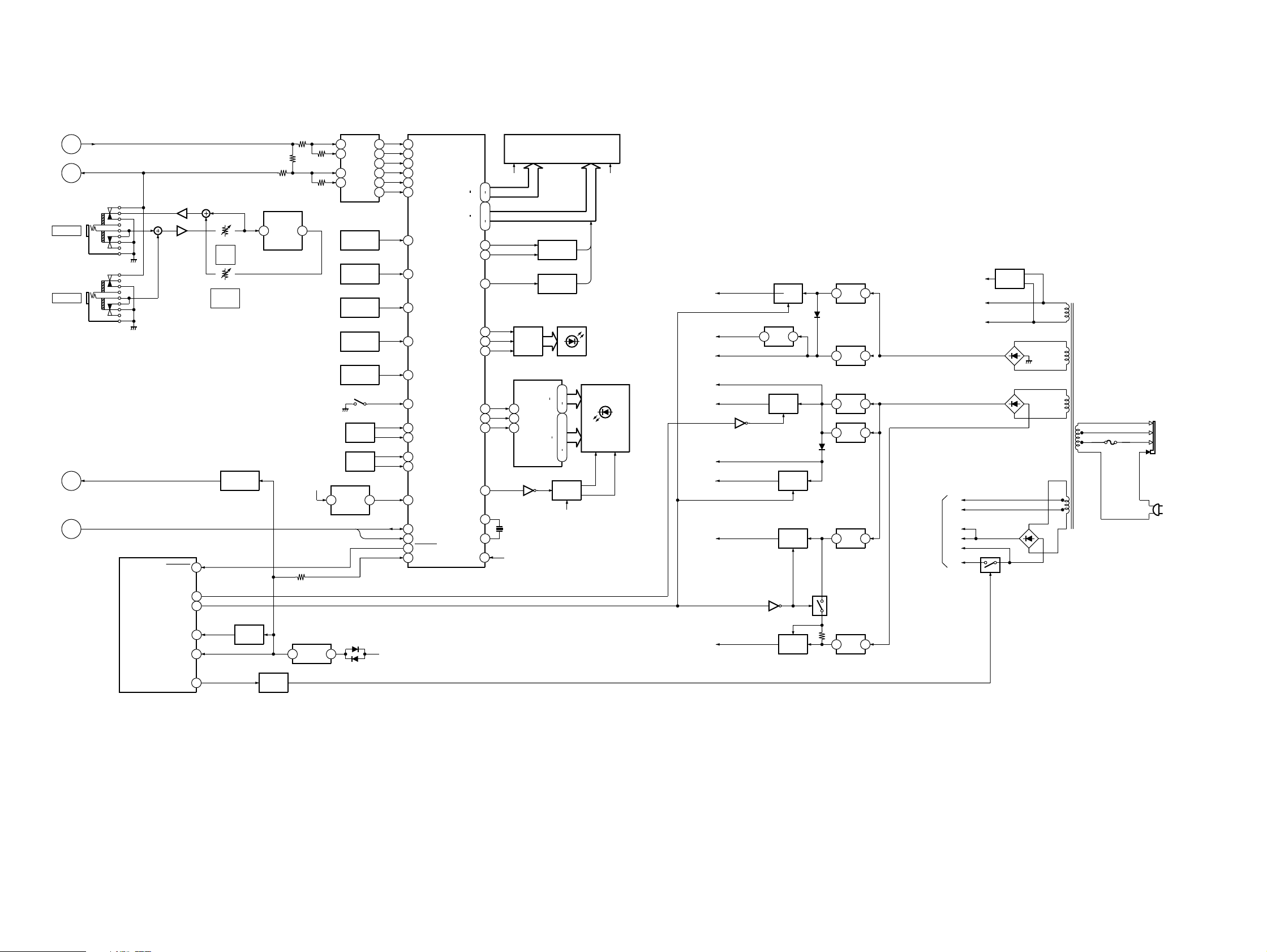
HCD-LV100AV
DISPLAY/POWER SECTION
J
K
L
D
SPA SIG
MIC SIG
TA MUTE
IIC DATA,IIC CLK
SYSTEM CONTROL
IC501(3/3)
MAIN
SECTION
(Page 22)
MAIN
SECTION
(Page 22)
MAIN
SECTION
(Page 22)
CD
SECTION
(Page 21)
J801
MIX MIC
J802
GUITAR
IC850
WAKE UP
DISPLAY CONTROL
IC601
6
5
4
3
ECHO
CONT
1 8
RV750
MIC
LEVEL
RV751
GUITAR
LEVEL
MUTE CONT
Q802
18
IC851
S621-624,626-630
S633,634,636,637,659
S617-619,654-659
S620,631,632,635
S651-653,667-671
+5V
3
REMOTE
CONTROL
RECEIVER
SPEANA
IC603
S601-604
S606-615
FUCTION
S641-647
S651-658
FUCTION
FUCTION
S676-682
FUCTION
FUCTION
S691
DOOR
S701
VOLUME
S791
CD JOG
IC702
BPF
KEY
KEY
KEY
KEY
KEY
17
16
14
13
12
11
1
IIC DATA
IIC CLK
16
17
18
19
20
21
11
12
13
14
15
80
9
10
2
8
1
78
79
22
73
BPF0
BPF1
BPF2
BPF3
BPF4
ALL BAND
KEY0
KEY1
KEY2
KEY3
KEY4
DSW
VOL A
VOL B
JOG A
JOG B
SIRCS
IIC DATA
IIC CLOCK
WAKE UP
RESET
SEG1
SEG23
GR2
GR14
GR1
GR15
ECO LED
DAILY LED
REC LED
LED DATA
LED SCK
LED LATCH
LED SEL
VKK
F1 F2
45
67
42
.
40
29
43
28
27GR16
Q605-607
77
74
75
5
3
4
7
XIN
70
72XOUT
68
13
14
15
X601
12.5MHz
VP
DRIVER
INDICATOR TUBE
LED
LED DRIVER
IC701
DATA
CLK
STB
Q601
FL601
FLOURESCENT
GRID BUFF
Q608-610
GRID BUFF
Q608
D601-603
17
.
P1
19
P5
22
1
.
3
P7
5
.
P16
7
11
LED +B
SWITCH
Q602,603
+5V
D623-627,635-638
D698,699,780
10V
12V
NEGATIVE
VP
VOL REG
Q903
F1
F2
D833-836
D841-844
D831
Q834
T951
MAIN TRANS
F951
S901
VOLTAGE
SELECTOR
230-240V
220V
120V
AC
IN
D912
IC931
+10V
3
1
REG
IC932
+12V
3
1
REG
IC921
+5V
3
1
REG
IC911
+5V
3
1
REG
+VL
-VL
IC901
+7V
3
1
REG
SURR/POWER
AMP
+VH
+VCC
-VH
-VCC
TUNER +B
SWITCH
Q931,932
D931
IC933
+7V
Q914
3
REG
CD +B SW
Q921
+B SW
Q911,912
+B SW
Q901,902
1
7V
5V
5V
5V
5V
7V
CD POWER
POWER
RESET
AC CUT
STK POWER
5
2
12
22
1
RESET
SWITCH
Q801
STBY
SWITCH
Q803,804
IC801
RESET
3
D803
1
+5V
D805
-7V
Q906
-B SW
Q903,904
Q905
IC951
-7V
3
2
REG
2424
HCD-LV100AV
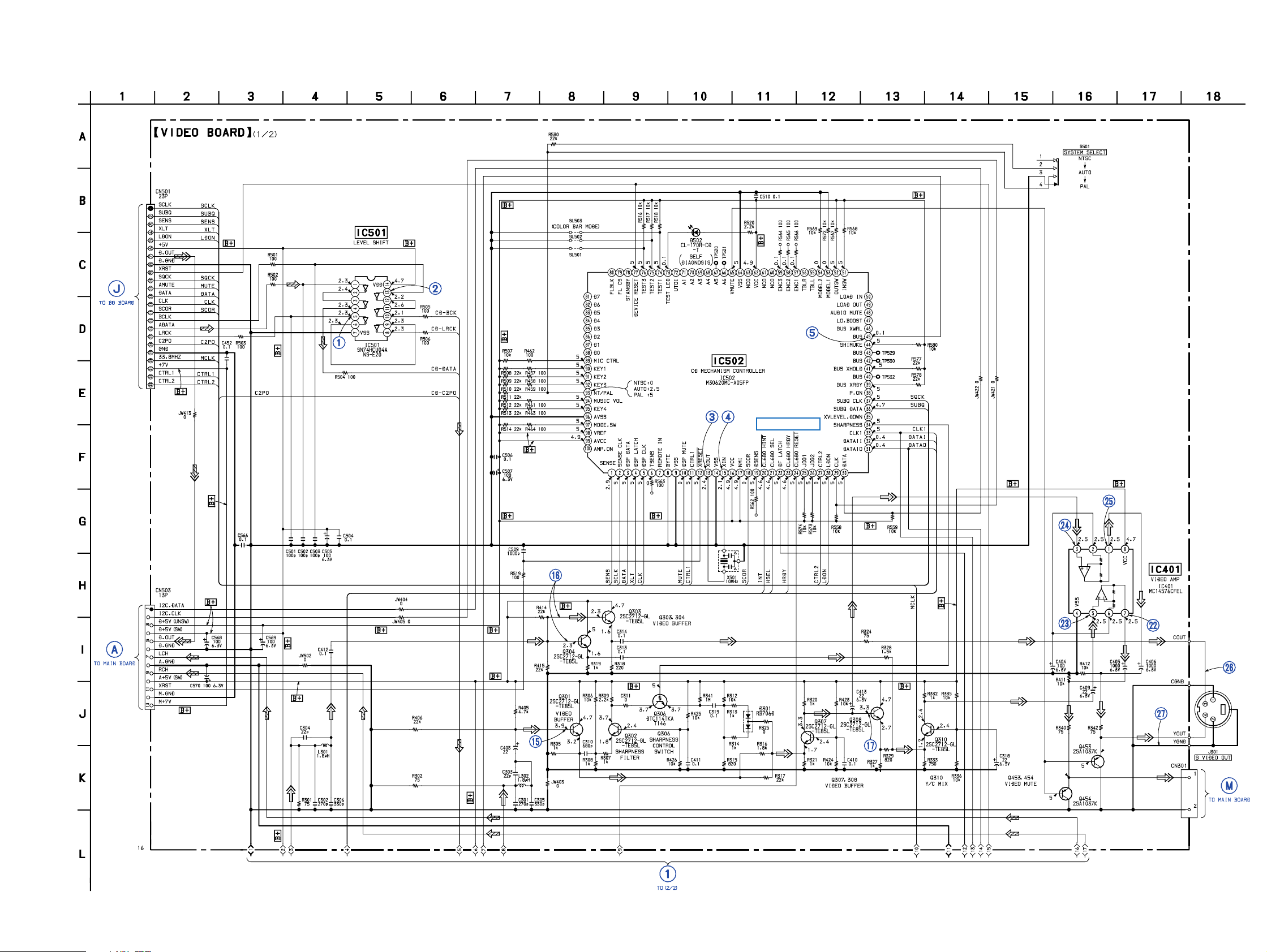
6-3. SCHEMATIC DIAGRAM VIDEO Board (1/2)
(Page 29)
• See page 39 for Waveforms.
• See page 59 for IC Pin Function Description.
(Page 37)
PIN FUNCTION
3
3
(Page 36)
• Voltages and waveforms are dc with respect to ground
under no-signal conditions.
no mark : VIDEO CD PLAY
2525
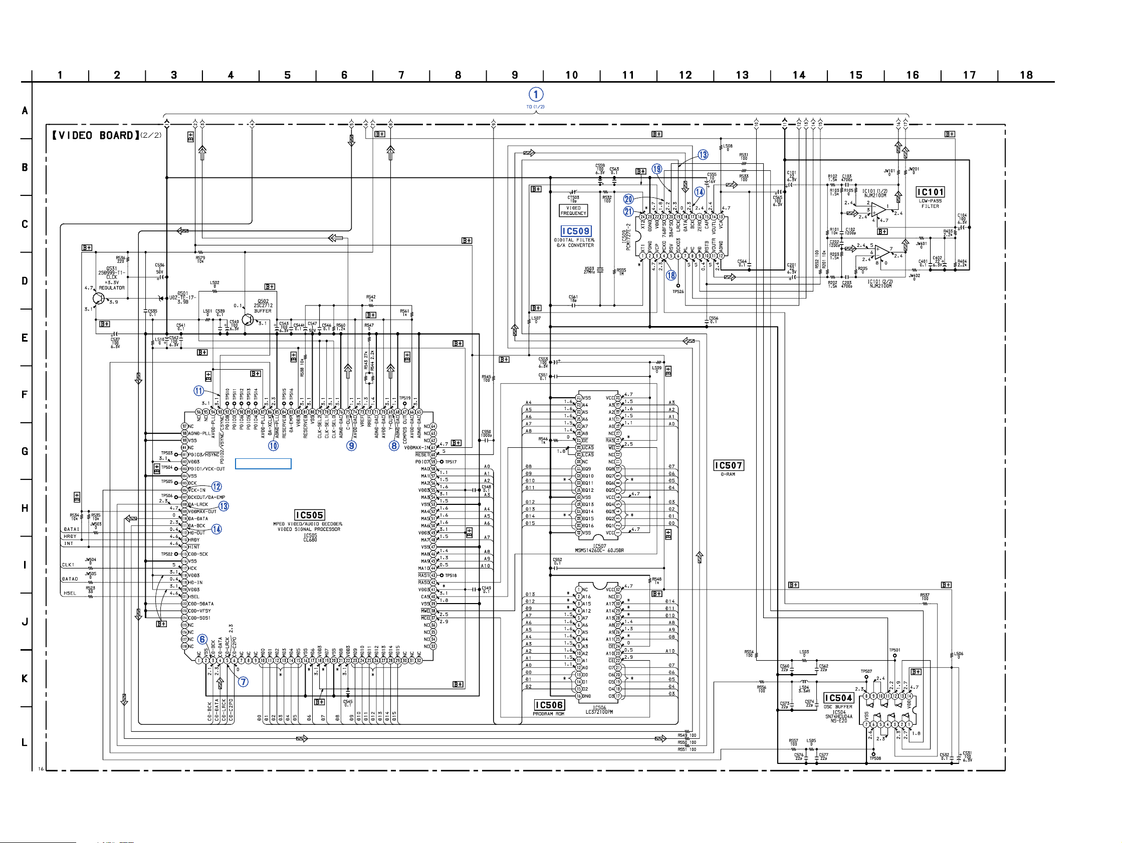
HCD-LV100AV
6-4. SCHEMATIC DIAGRAM VIDEO Board (2/2)
• See page 39 for Waveforms. • See page 55 for IC Block Diagram.
• See page 61 for IC Pin Function
PIN FUNCTION
• Voltages and waveforms are dc with respect to ground
under no-signal conditions.
no mark : VIDEO CD PLAY
* : Impossible to measure
2626
HCD-LV100AV
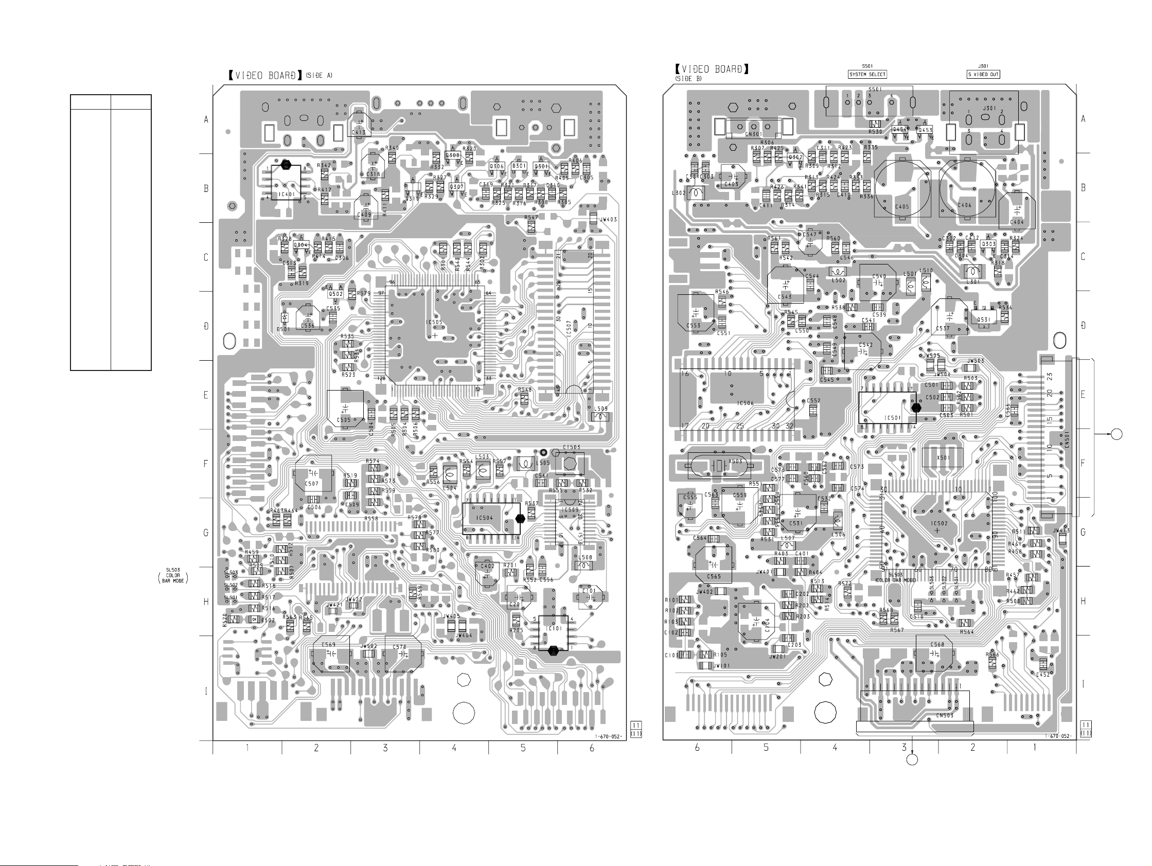
6-5. PRINTED WIRING BOARD VIDEO Board
• Semiconductor
Location
Ref. No. Location
D301 B-5(A)
D501 D-2(A)
D502 H-1(A)
IC101 H-5(A)
IC401 B-2(A)
IC501 E-3(B)
IC502 G-3(B)
IC504 G-4(A)
C505 D-4(A)
IC506 E-5(B)
IC507 D-5(A)
IC509 G-5(A)
Q301 B-5(A)
Q302 B-5(B)
Q303 C-2(B)
Q304 C-2(A)
Q306 B-4(A)
Q307 B-4(A)
Q308 B-4(A)
Q310 B-3(A)
Q453 A-3(A)
Q454 A-3(A)
Q502 D-2(A)
Q531 D-2(B)
• See page 20 for Circuit Board Location.
TP508
(27MHz)
A
TO
BD BOARD
(Page 28)
16
16
J
TO
MAIN BOARD
(Page 35)
2727
HCD-LV100AV
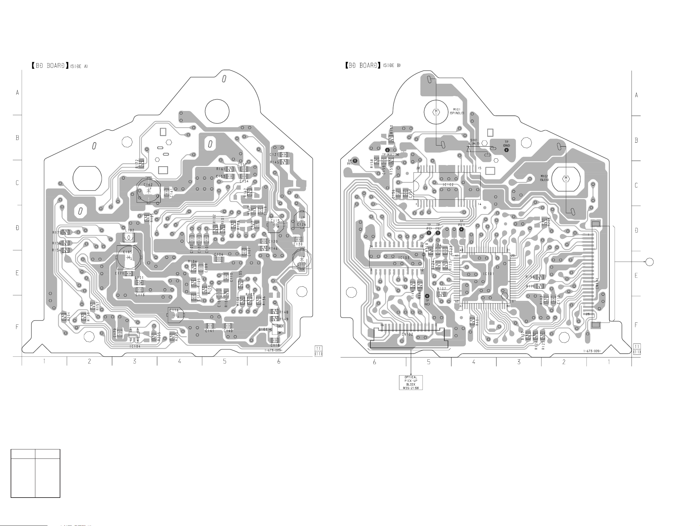
6-6. PRINTED WIRING BOARD BD Board
• See page 20 for Circuit Board Location.
16
• Semiconductor
Location
Ref. No. Location
IC101 E-4(B)
IC102 C-5(B)
IC103 E-6(B)
IC104 F-3(A)
A
TO
VIDEO
BOARD
(Page 27)
16
Q101 F-6(A)
2828
 Loading...