

Page 1
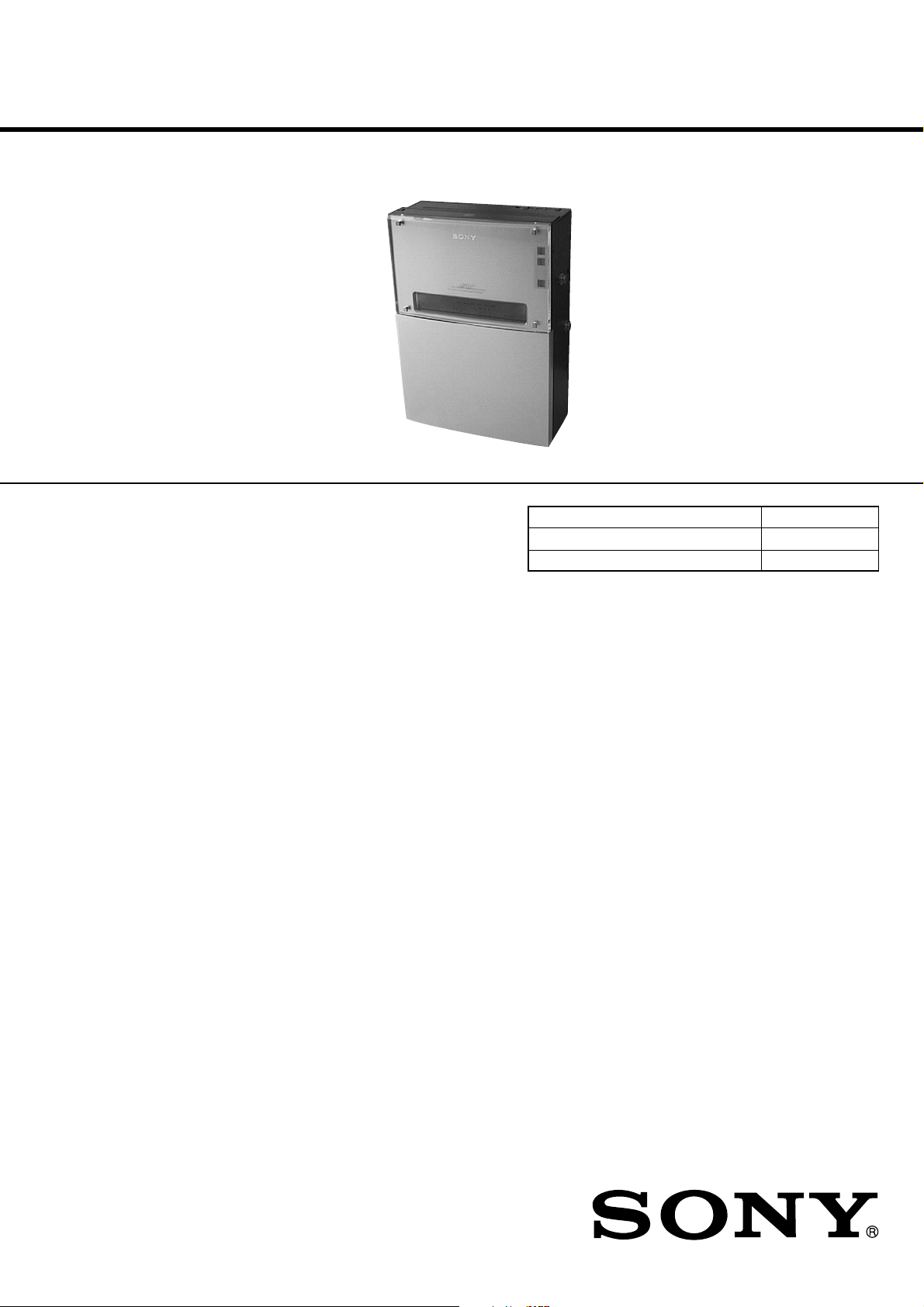
HCD-LS1
SERVICE MANUAL
HCD-LS1 is the Amplifier, CD player and
Tuner section in CMT-LS1.
SPECIFICATIONS
US Model
Canadian Model
AEP Model
UK Model
E Model
Model Name Using Similar Mechanism NEW
CD Mechanism Type HG-1
Optical Pick-up Name KSS-540A
Amplifier section
For the U.S. model
AUDIO POWER SPECIFICATIONS
POWER OUTPUT AND TOTAL HARMONIC
DISTORTION:
With 4 ohm loads both channels driven, from 120 –
10,000 Hz; rated 10 watts per channel minimum
RMS power, with no more than 10% total
harmonic distortion from 250 milliwatts to rated
output.
North American model:
Continuous RMS power output (Reference)
European model:
DIN power output (Rated) 11 + 11 watts
Continuous RMS power output (Reference)
Other models:
DIN power output (Rated) 11 + 11 watts
Continuous RMS power output (Reference)
16 + 16 watts
(4 ohms at 1 kHz, 10% THD)
(4 ohms at 1 kHz, DIN)
16 + 16 watts
(4 ohms at 1 kHz, 10% THD)
(4 ohms at 1 kHz, DIN, 240 V)
11 + 11 watts
(4 ohms at 1 kHz, DIN, 220 V)
16 + 16 watts
(4 ohms at 1 kHz, 10% THD,
240 V)
16 + 16 watts
(4 ohms at 1 kHz, 10% THD,
220 V)
Inputs TAPE IN (stereo mini jack):
Outputs TAPE OUT (stereo mini jack):
CD player section
System Compact disc and digital audio
Laser Semiconductor laser (λ=780 nm)
Laser output Max. 44.6 µW*
Frequency response 20 Hz – 20,000 Hz (±3.0 dB)
voltage 250 mV, impedance
47 kilohms
1Vrms at CD Full Bit Play,
impedance 1 kilohm
CD OUT: Optical
PHONES (stereo mini jack):
accepts headphones of 8 ohms or
more
SPEAKER: speaker system
4 ohms
system
Emission duration: continuous
*This output is the value measured
at a distance of 200 mm from the
objective lens surface on the
Optical Pick-up Block with 7 mm
aperture.
– Continued on next page –
COMPACT DISC RECEIVER
Page 2

Tuner section
FM stereo, FM/AM superheterodyne tuner
FM tuner section
Tuning range
North American model: 87.5 – 108.0 MHz (100 kHz step)
Other models: 87.5 – 108.0 MHz (50 kHz step)
Antenna FM lead antenna
Antenna terminals 75 ohms unbalanced
Intermediate frequency 10.7 MHz
AM tuner section
Tuning range
North American model: 530 – 1,710 kHz
European model: 531 – 1,602 kHz
Other models: 531 – 1,602 kHz
Antenna AM loop antenna
Intermediate frequency 450 kHz
(with the interval set at 10 kHz)
531 – 1,710 kHz
(with the interval set at 9 kHz)
(with the interval set at 9 kHz)
(with the interval set at 9 kHz)
530 – 1,710 kHz
(with the interval set at 10 kHz)
Desktop stand
Dimensions (w/h/d) 184 × 218 × 140 mm
Mass Approx. 0.5 kg
Wall hanging adapter
Dimensions (w/h/d) 180 × 220 × 39 mm
Mass Approx. 0.5 kg
Wall hanging bracket
Dimensions (w/h/d) 180 × 220 × 12 mm
Mass Approx. 0.4 kg
General
Power requirements
North American model: 120 V AC, 60 Hz
European model: 230 V AC, 50/60 Hz
Other models: 220 – 240 V AC, 50/60 Hz
Power consumption 25 W
Dimensions 192 × 295 × 150 mm
Mass Approx. 4.0 (with Desktop
Supplied accessories Remote commander (1)
(w/h/d, incl. projecting parts,
controls and desktop stand)
stand) kg
AM loop antenna (1)
FM wire antenna (1)
Desktop stand (1)
Wall hanging adapter (1)
Wall hanging bracket (1)
Screws for stand or adapter
M4 ×14 (4)
Dust caps (3)
TABLE OF CONTENTS
1. SERVICING NOTES ............................................... 3
2. GENERAL ................................................................... 5
3. DISASSEMBLY ......................................................... 7
4. ELECTRICAL ADJUSTMENT............................ 19
5. DIAGRAMS
5-1. Note for Printed Wiring Boards and
Schematic Diagrams ....................................................... 21
5-2. Printed Wiring Board – CD Section – ........................... 22
5-3. Schematic Diagram – CD Section (1/3) – ..................... 23
5-4. Schematic Diagram – CD Section (2/3) – ..................... 24
5-5. Schematic Diagram – CD Section (3/3) – ..................... 25
5-6. Printed Wiring Board – Main Section – ........................ 26
5-7. Schematic Diagram
– MAIN Section – ........................................................... 27
5-8. Printed Wiring Boards
– AMP/RELA Y/JACK Board – ...................................... 28
5-9. Schematic Diagram
– AMP/RELA Y/JACK Board – ...................................... 29
5-10. Printed Wiring Boards – Panel Section (1/2) – ............. 30
5-11. Schematic Diagram – Panel Section (1/2) –.................. 31
5-12. Printed Wiring Boards – Panel Section (2/2) – ............. 32
5-13. Schematic Diagram – Panel Section (2/2) –.................. 32
5-14. Printed Wiring Boards
– POWER SUPPLY Section – ....................................... 34
5-15. Schematic Diagram – POWER SUPPLY Section –....... 35
6. EXPLODED VIEWS ................................................ 37
7. ELECTRICAL PARTS LIST ............................... 43
Designs and specifications are subject to change
without notice.
SAFETY-RELATED COMPONENT WARNING!!
COMPONENTS IDENTIFIED BY MARK 0 OR DOTTED
LINE WITH MARK 0 ON THE SCHEMATIC DIA GRAMS
AND IN THE PARTS LIST ARE CRITICAL TO SAFE
OPERATION. REPLACE THESE COMPONENTS WITH
SONY PARTS WHOSE PART NUMBERS APPEAR AS
SHOWN IN THIS MANUAL OR IN SUPPLEMENTS PUBLISHED BY SONY.
2
ATTENTION AU COMPOSANT AYANT RAPPORT
À LA SÉCURITÉ!
LES COMPOSANTS IDENTIFIÉS P AR UNE MARQUE 0
SUR LES DIAGRAMMES SCHÉMA TIQUES ET LA LISTE
DES PIÈCES SONT CRITIQUES POUR LA SÉCURITÉ
DE FONCTIONNEMENT. NE REMPLACER CES COMPOSANTS QUE PAR DES PIÈCES SONY DONT LES
NUMÉROS SONT DONNÉS DANS CE MANUEL OU
DANS LES SUPPLÉMENTS PUBLIÉS PAR SONY.
Page 3
SECTION 1
SERVICING NOTES
SAFETY CHECK-OUT
After correcting the original service problem, perform the following safety check before releasing the set to the customer:
Check the antenna terminals, metal trim, “metallized” knobs,
screws, and all other exposed metal parts for AC leakage.
Check leakage as described below.
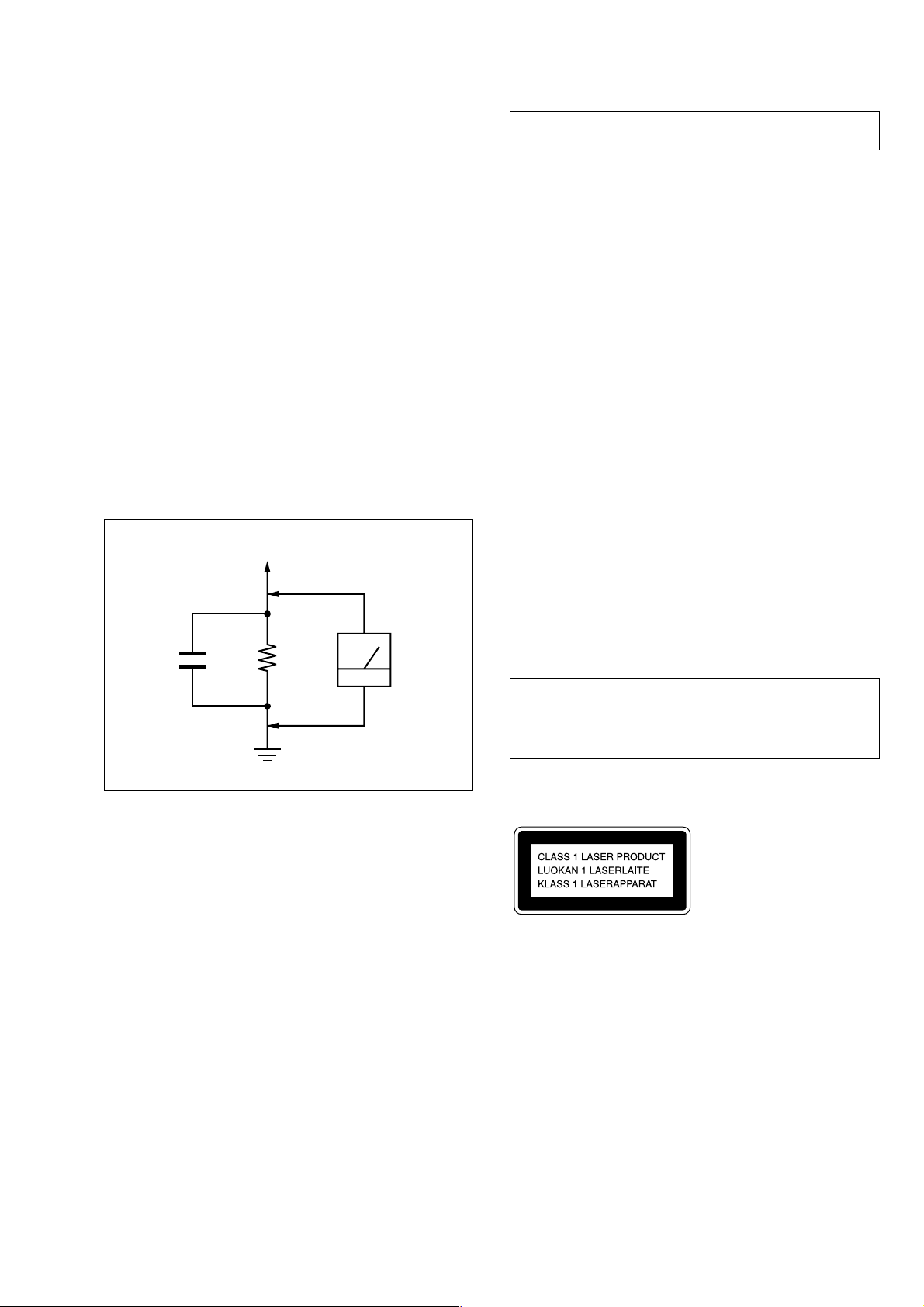
LEAKAGE TEST
The AC leakage from any exposed metal part to earth ground and
from all exposed metal parts to any exposed metal part having a
return to chassis, must not exceed 0.5 mA (500 microamperes.).
Leakage current can be measured by any one of three methods.
1. A commercial leaka ge tester, such as the Simpson 229 or RCA
WT -540A. Follo w the manufacturers’ instructions to use these
instruments.
2. A battery-operated AC milliammeter. The Data Precision 245
digital multimeter is suitable for this job.
3. Measuring the voltage drop across a resistor by means of a
VOM or battery-operated AC voltmeter. The “limit” indication is 0.75 V, so analog meters must have an accurate lowvoltage scale. The Simpson 250 and Sanwa SH-63Trd are examples of a passive VOM that is suitable. Nearly all battery
operated digital multimeters that have a 2 V A C range are suitable. (See Fig. A)
To Exposed Metal
Parts on Set
NOTES ON HANDLING THE OPTICAL PICK-UP
BLOCK OR BASE UNIT
The laser diode in the optical pick-up block may suffer electrostatic break-down because of the potential difference generated
by the charged electrostatic load, etc. on clothing and the human
body.
During repair, pay attention to electrostatic break-down and also
use the procedure in the printed matter which is included in the
repair parts.
The flexible board is easily damaged and should be handled with
care.
NOTES ON LASER DIODE EMISSION CHECK
The laser beam on this model is concentrated so as to be focused
on the disc reflective surface by the objective lens in the optical
pick-up block. Therefore, when checking the laser diode emission, observe from more than 30 cm away from the objective lens.
Notes on chip component replacement
• Never reuse a disconnected chip component.
• Notice that the minus side of a tantalum capacitor may be damaged by heat.
Flexible Circuit Board Repairing
• Keep the temperature of the soldering iron around 270 ˚C during repairing.
• Do not touch the soldering iron on the same conductor of the
circuit board (within 3 times).
• Be careful not to apply force on the conductor when soldering
or unsoldering.
1.5 k
0.15 µF
Fig. A. Using an AC voltmeter to check AC leakage.
Ω
Earth Ground
AC
voltmeter
(0.75 V)
CAUTION
Use of controls or adjustments or performance of procedures
other than those specified herein may result in hazardous radiation exposure.
This appliance is classified as a CLASS 1 LASER product.
The CLASS 1 LASER PRODUCT MARKING is located on
the rear exterior.
3
Page 4
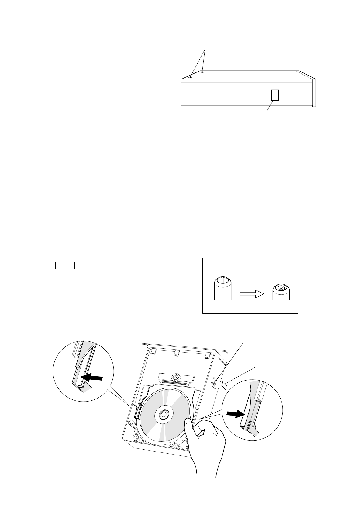
DISC EJECTION IN EMERGENCY
L
In case of emergency , remove the discs inside the Mec hanism Ass’y
(CD Changer) as follows:
(1) Disconnect the power of the Main Unit.
(2) Remove the Mechanism Ass’y. Refer to item
(3) Remove two top cover fastening screws at the rear of the
Mechanism Ass’y, and tak e off the Top Cover HS Ass’y . Refer
to Fig. A.
(4) Remove the left side adhesive label (Dust Seal EMA SL) on
the left side of the Mechanism Ass’y. Refer to Fig. A.
Note: Carefully remove it since it is used again later.
(5) Turn the Emergency Gear SL up or down until the disc lock
sleeve SL is lowered as shown in Fig. B.
Caution:Never use nail when turning the Emergency Gear
SL. Otherwise, the gear tooth may be broken.
(6) Raise the front section of the Mechanism Ass’y as illustrated
in Fig. B. Then carefully spread the Loading L/R MF Ass’y so
that the disc drops into the Stocker.
(7) While keeping the Loading L/R MF Ass’y spread, remov e the
discs.
Note: When removing the discs, take care not to scrape them
against other parts, to prevent damage.
(8) Re place the removed parts by reversing the above procedure.
Note: To prevent dust from entering the unit, reattach the
adhesive label on the opening for the Emergency Gear
SL.
(9) Perform the mechanism initialization as follows to clear the
disc information stored in the Mechanism Ass’y.
Press the DISC1 button while pressing the DISC5 button.
Then, the Unit enters the CD Playback mode and mechanism
Initialization operation begins and disc change operation starts.
After that, the Unit enters Standby mode.
DISC1 + DISC5
Top Cover Fastening Screws
Label
Fig. A
Disc Lock Sleeve SL
Loading R MF Ass’y
– Up Position –– Down Position –
Emergency Gear SL
Dust Seal EMA S
Loading L MF Ass’y
Fig. B
4
Page 5
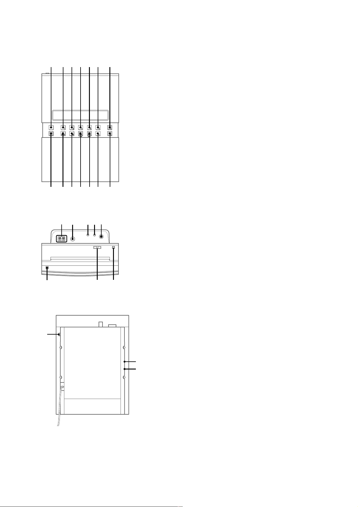
• LOCATION OF CONTROLS
– Front View –
SECTION 2
GENERAL
1 23456 7
8 9 q; qa qs qd qf
– Top View –
54321
678
1 FUNCTION button
2 DISC 1 button and indicator
3 DISC 2 button and indicator
4 DISC 3 button and indicator
5 DISC 4 button and indicator
6 DISC 5 button and indicator
7 VOLUME + button
8 TUNER/BAND button
9 u button and indicator
q; x button
qa . m , TUNER - button
qs > M , TUNER + button
qd A button
qf VOLUME - button
1 AM ANTENNA terminals
2 FM ANTENNA jack
3 TAPE OUT jack
4 TAPE IN jack
5 PHONES jack
6 `/1 button
7 PANEL OPEN switch
8 PANEL OPEN/CLOSE switch
– Rear View –
1
1 CD DIGITAL OUT (OPTICAL) connector
2 LEFT SPEAKER terminals
3 RIGHT SPEAKER terminals
2
3
5
Page 6
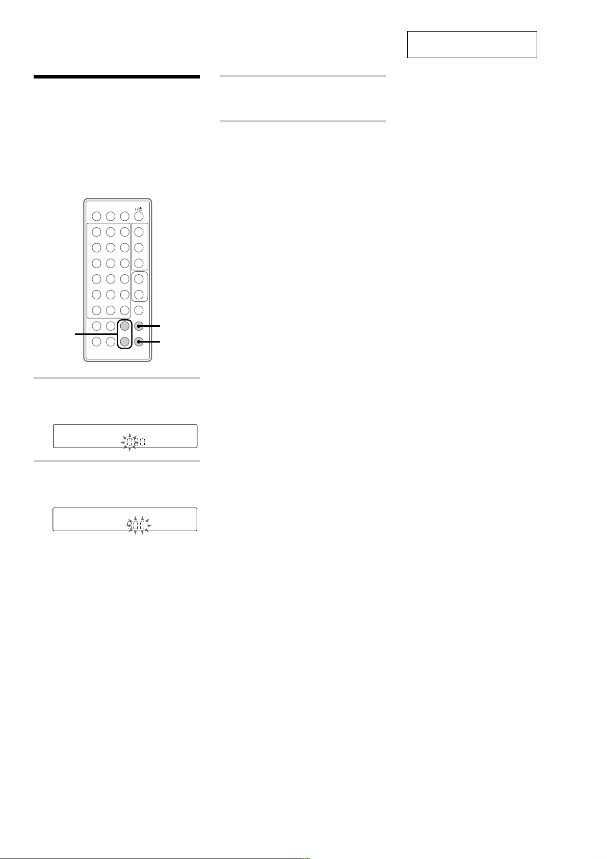
Step 2: Setting the time
You must set the time before you can use the
timer functions.
The clock is on a 24-hour system for the European
model, and a 12-hour system for other models.
The 24 hour system model is used for illustration
purposes.
Set the time before turning on the power.
31
2
564
8
97
10/0
>10
+
X
x
+
–
.>
M
+
–
–
1
2,3
N
m
2,3
3
Press +/– to set the minute then press
ENTER.
The clock starts.
To change the time
You can change the preset time while the power is
on.
1 Press CLOCK/TIMER SET.
2 Press +/– repeatedly until “SET CLOCK”
appears then press ENTER.
3 Repeat steps 2 and 3 of “Setting the time”.
Tips
• If you have made a mistake, start again from step 1.
• The built-in clock shows the time in the display
while the power is off.
• The upper dot flashes for the first half of a minute
(0 to 29 seconds), and the lower dot flashes for the
last half of a minute (30 to 59 seconds).
This section is extracted from
instruction manual.
1
Press CLOCK/TIMER SET while the
power is off.
The hour indication flashes.
2
Press +/– to set the hour then press
ENTER.
The minute indication flashes.
6
Page 7
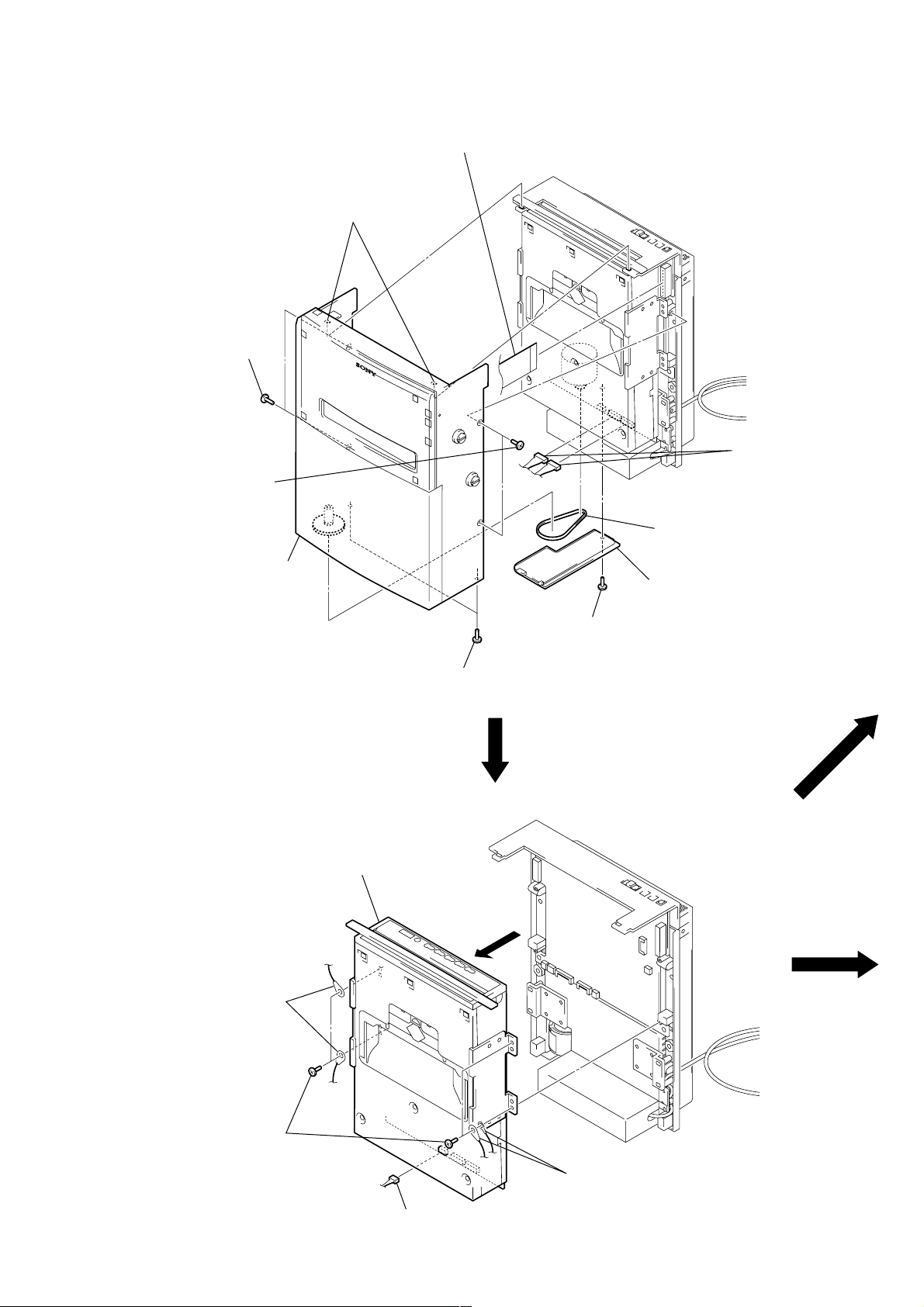
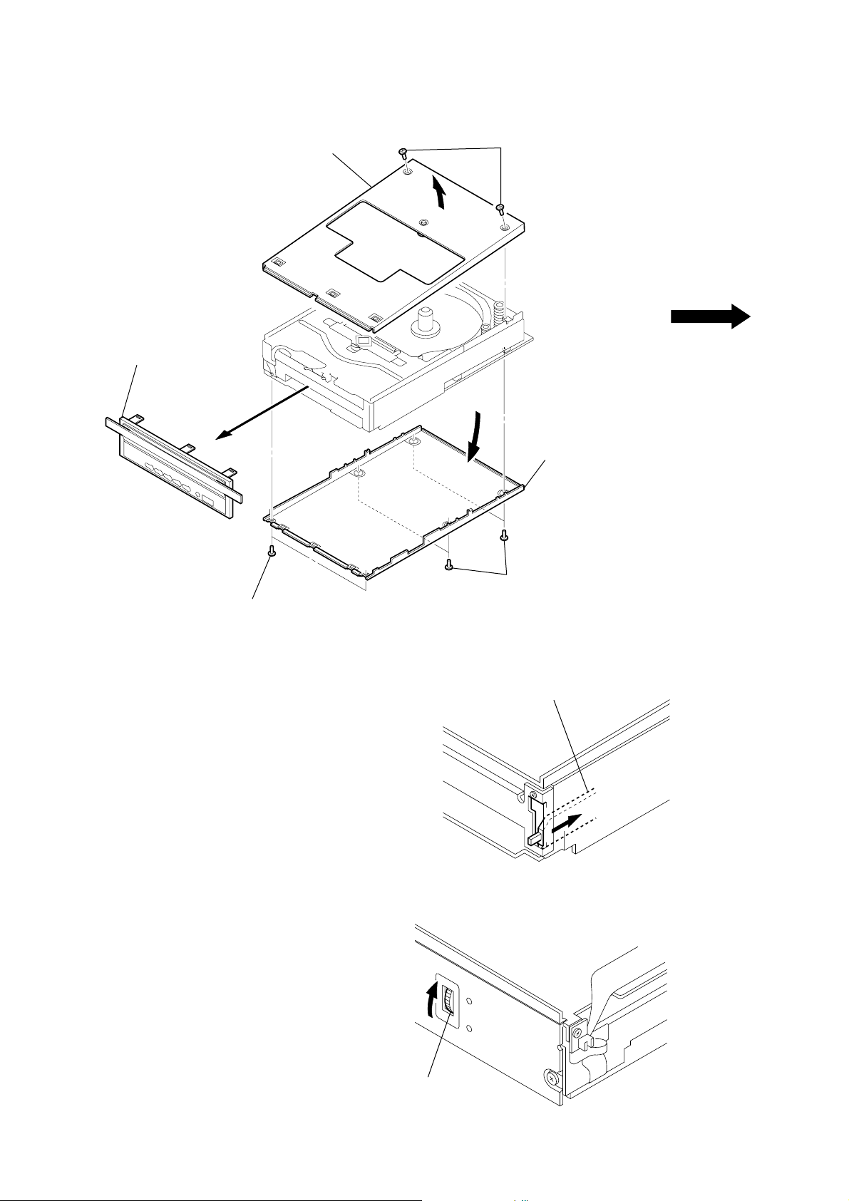
SECTION 3
DISASSEMBLY
Note: Follow the disassembly procedure in the numerical order given.
MAIN CASE SECTION
5 two screws
(BTP 3 × 10)
5 two screws
(BTP 3 × 10)
9 main case section
7 FFC (26core)
(CN604)
6 two claws
8 two connectors
(PC501, 502)
3 belt
2 bottom cover
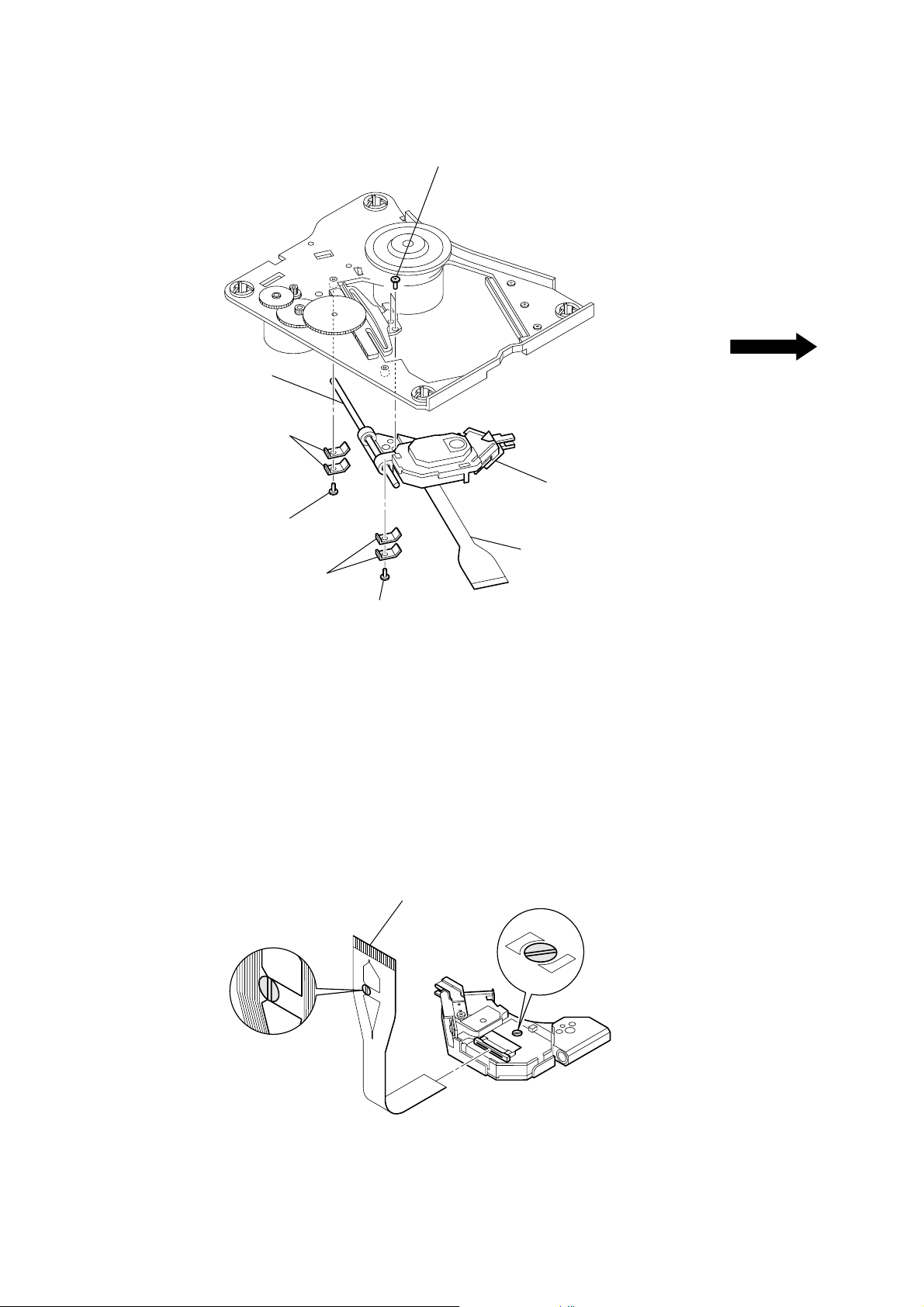
MECHANISM DECK (HG-1)
2 two lugs
1 screw
(B3 × 6)
4 two screws
(BTP 3 × 10)
DOOR MOTOR ASS’Y (M391) (Ne xt P age)
HOLDER MECHA, DUST SEAL EMA SL
(Page 9)
5 mechanism deck (HG-1)
3
1 four screws
(BTP 3 × 10)
2 two lugs
4 connector
(CP503)
7
Page 8
DOOR MOTOR ASS’Y (M391)
(
)
7 door motor ass’y
(M391)
6 motor bracket
2 two screws
(BTP3 × 8)
1 connector
(CN391)
4
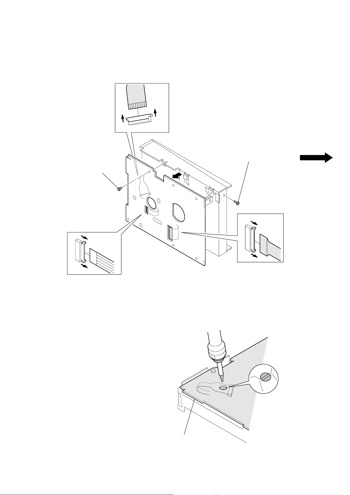
MAIN BOARD
4 Remove the MAIN board
in the direction of the arrow.
3 lug
1 FFC (15core)
(CN101)
S391
5 two screws
(P2.6 × 3)
Note: On installation MAIN board
adjust the S391 and slide knob.
slide knob
2 two connectors
(CN201, 204)
2 five connectors
CN203, 301, 302, 303, 391
3 two screws
(PWH2.6 × 6)
8
Page 9
(1) MODE-1
EJECT, DISC LOAD state
(2) MODE-2
STANDARD State (STOP state)
(3) MODE-3
PLAY, DISC CHANGE state
When disassembling and reassembling the mechanism deck by any failure, the mechanism deck must be in (2) Standard
state (STOP state) as shown below.
• The mechanism deck (HG-1) has three modes. (Fig. A)
mecha UD sub cam SL
Traverse Mecha Down state
Traverse Mecha Up state
sus base X sub ass’y shaft
(Fig. A)
HOW TO ADJUST STOP STATE POSITION
D lock sleeve SL
emergency gear SL
2 Rotate gradually the emergency
gear SL in the up arrow direction
up to the position where the D lock
sleeve SL comes to the bottom.
(To attain (2) standard state in Fig. A)
1 Rotate fully the emergency gear SL
in the down arrow direction.
HOLDER MECHA, DUST SEAL EMA SL
1 four screws
(B3 × 5)
3 dust seal EMA SL
Note:Carefully remove it since
it is used again later.
2 holder mecha
2 holder mecha
PRECAUTIONS ON DISASSEMBLING AND REASSEMBLING MECHANISM DECK
1 four screws
(B3 × 5)
9
Page 10
TOP COVER HS ASS’Y, BOTTOM COVER MF ASS’Y, F PANEL ASS’Y R237
2 Remove top cover HS ass’y
in the direction of arrow A.
A
5 F panel ass’y R237
1 two screws
(P2.6 × 3)
B
4 Remove bottom cover
MF ass’y in the direction
of arrow B.
3 two screws
(P2.6 × 5)
Note: 1.Before reassembling F Panel Ass’y R237
be sure that the end of the Mecha UD Sub
Cam SL on the right front does not protrude
as shown in (Fig. B.1). If it protrudes, move
it backward as follows:
1) Carefully remove the left side adhesive
label (Dust Seal EMA SL) on the left side
of the unit. refer to (Fig. B.2)
2) Turn the Emergency Gear SL with your
finger tip in the direction of the arrow
until the end of the Mecha UD Sub Cam
SL is drawn inside the unit. (See Fig. B.2).
When turning the Gear, DO NOT use nail
as the gear tooth can be broken.
3) Reattach the adhesive label (Dust Seal EMA
SL).
Note: 2.Be sure that the claws of F Panel Ass’y R237 are
securely inserted into each holes in Top Cover HS
Ass’y and Bottom Cover MF ass’y.
3 four screws
(P2.6 × 5)
Mecha UD Sub SL
(Fig. B.1)
10
Emergency Gear SL
(Fig. B.2)
Page 11
MAIN R237 BOARD
(
)
y
MAIN R237 board
Unsolder the shorting lands
on the pick-up flexible board.
Note: To allow easier installation of the MAIN R237 board,
move the optical pick-up KSS-540A to the outermost
position, before removing the MAIN R237 board.
6 pick-up flexible board
(CP101)
2 screw
(P2.6 × 4)
4 wire flexible board
CP102
Note: When disconnecting these felxible boards,
do not open the MAIN R237 board wide to
avoid damage to flexible boaards.
1 screw
(P2.6 × 8)
3
5 PCB FLEX mecha ass’
(CP103)
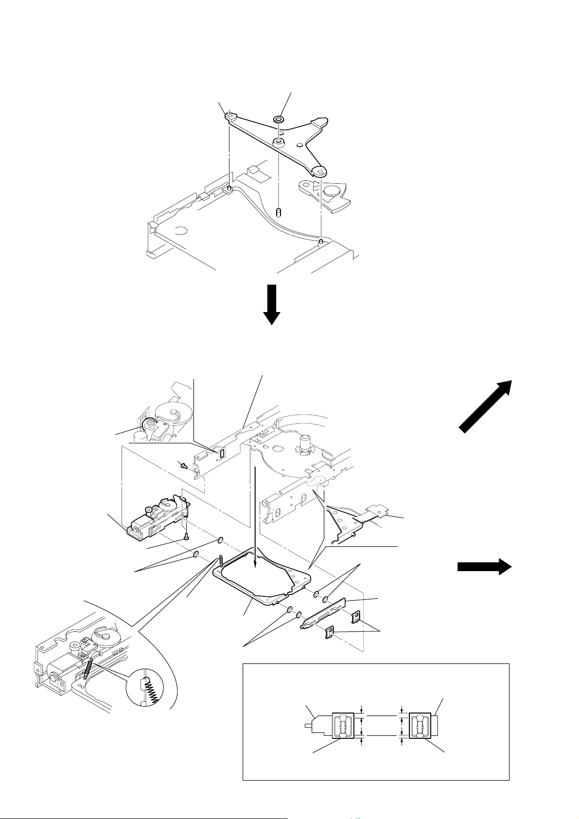
LOADING MF ASS’Y
(Next Page)
STC POS GEAR SL
(Page 18)
INSTALLING THE MAIN R237 BOARD
11
Page 12
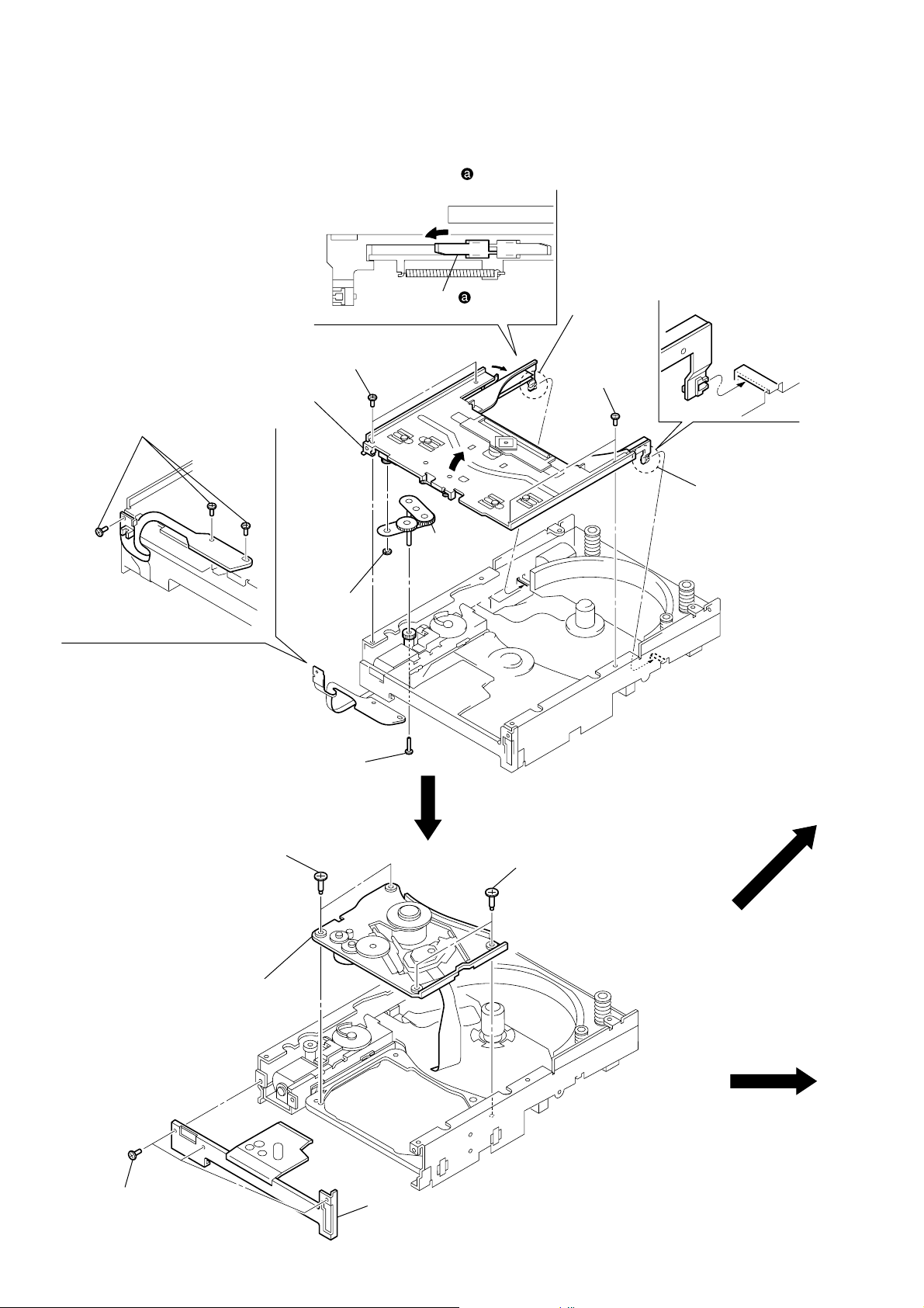
LOADING MF ASS’Y
Note:Though the cam of the Mecha UD sub cam SL will be in (1) state in (Refer to page 9. Fig. A)
when the loading MF Ass’y is assembled, set in (2) state in (Refer to page 9. Fig. A) using
the emergency gear SL.
6 While pushing lever inward, remove
loading MF ass’y by lifting it upward.
1 three screws
(P2 × 2)
2 two screws
(2.6 × 3)
7 loading MF ass’y
8 washer
lever
4
9 loading link
SL ass’y
5 ditch
2 two screws
(2.6 × 3)
5 ditch
TRAVERSE MECHA ASS’Y
3 two damper screws
4 traverse mecha ass’y
1 three screws
(P2 × 2)
3 screw
(P1.7 × 2.5)
3 two damper screws
PCB FLEX MECHA
ASS’Y
(Page 15)
2 FR chassis SL ass’y
12
Page 13
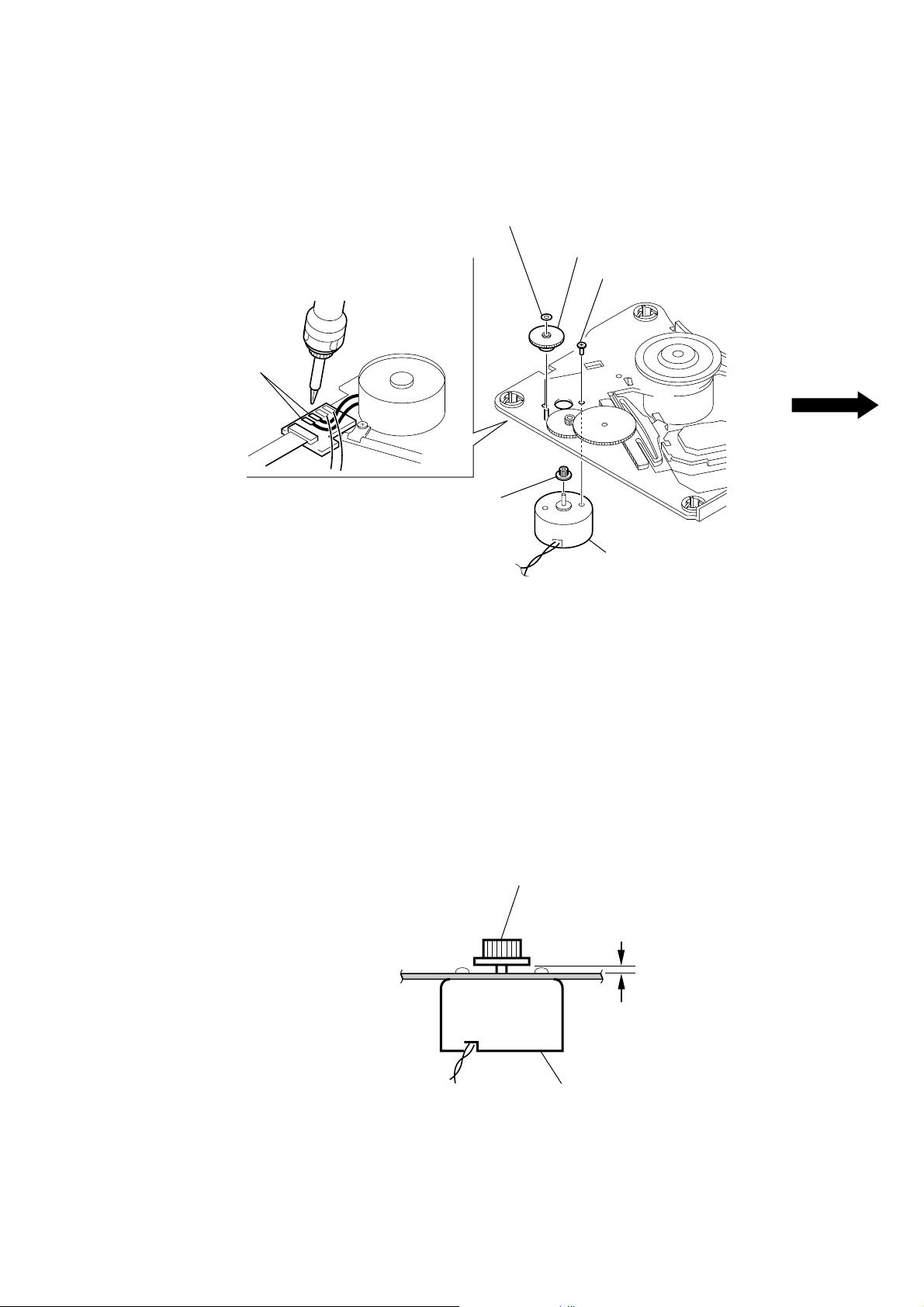
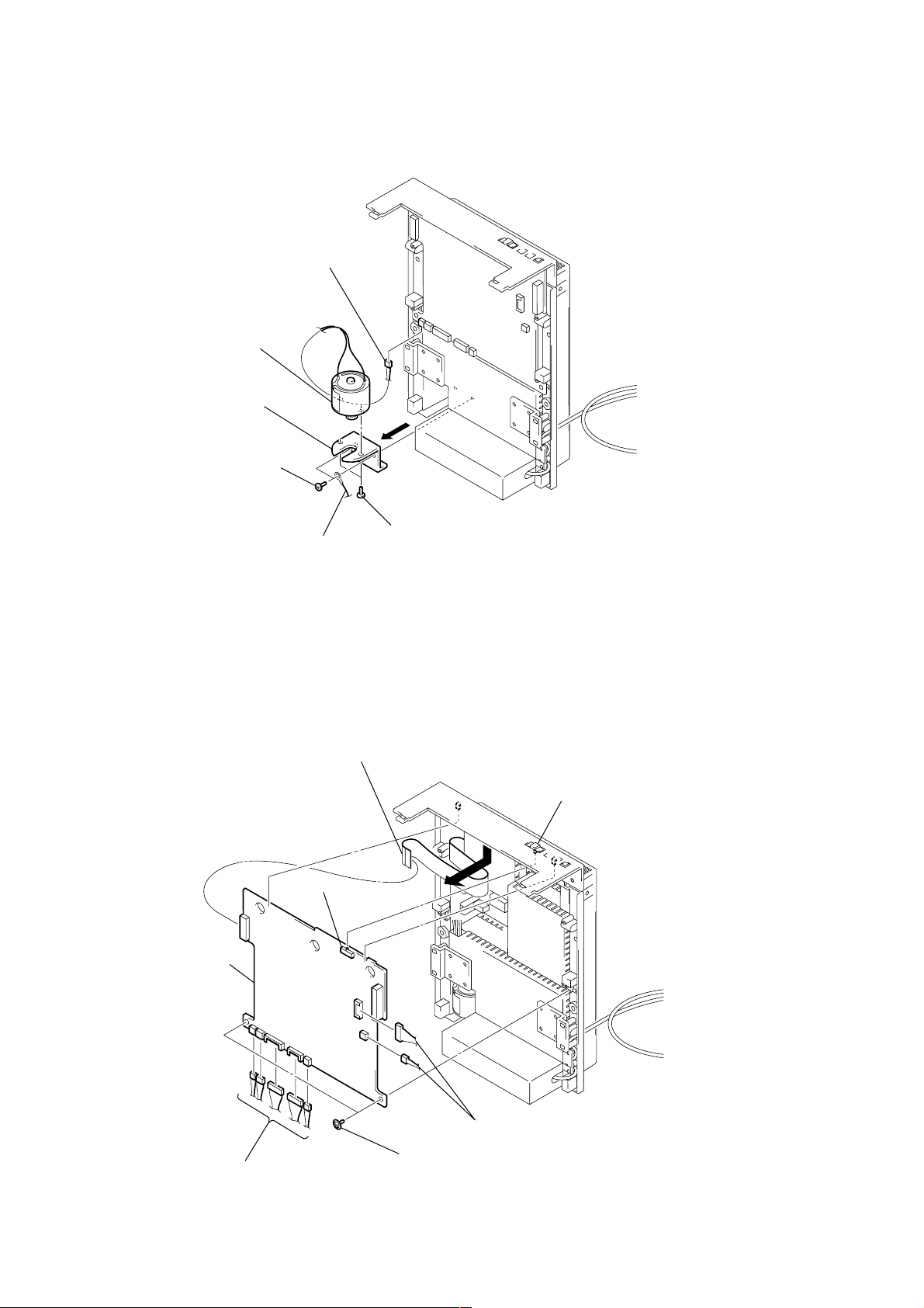
MOTOR (SLED) (M1)
1 Remove two solders of
the sled motor leads (M1).
2 washer
5 first gear
Note:When first gear is removed,
make sure to install a bland
new gear.
3 second gear
4 two screws
(P1.7 × 2.5)
6 motor (sled)
(M1)
Note:Pay attention to the motor (sled)
installing direction.
INSTALLING A MOTOR (SLED) (M1)
Note: Press fit a new first gear so that the gap
between the chassis surface and the bottom
of first gear is 0.1mm as shown in Fig. C.
first gear
0.1 mm
motor (sled) (M1)
(Fig. C)
13
Page 14
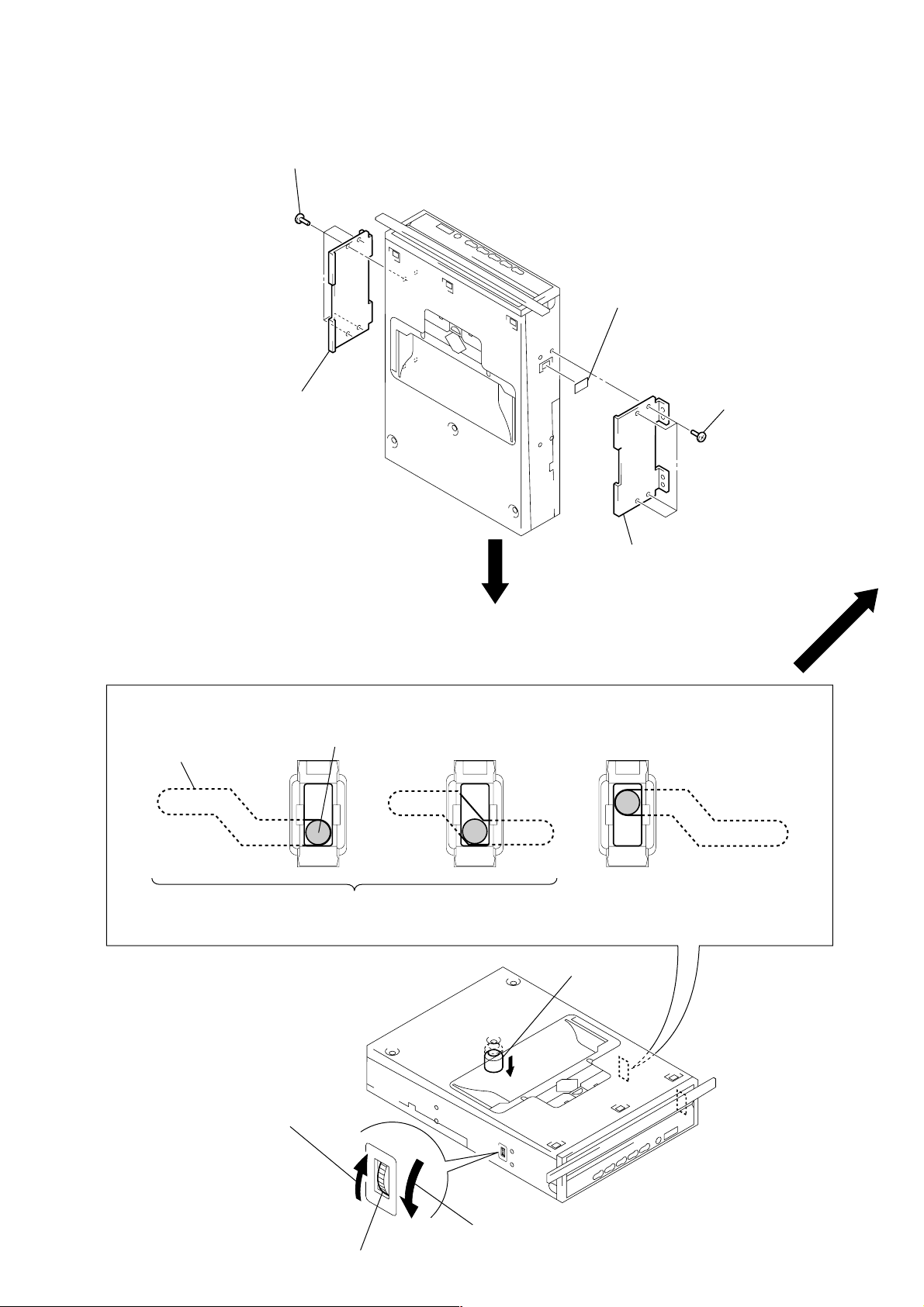
OPTICAL PICK-UP KSS-540A
4 PU guide shaft SL
3 two SH lock plate SLs
2 screw
(P2.6 × 3)
3 two SH lock plate SLs
2 screw
(P2.6 × 3)
1 two screws
(P1.7 × 4)
6 optical pick-up KSS-540A
5 pick-up flexible board
Note: Before disconnecting the pick-up
flexible board from the optical pick-up
KSS-540A, short the laser diode
shorting lands on the bottom of the
optical pick-up KSS-540A.
Refer to Fig. D.
INSTALLING A OPTICAL PICK-UP KSS-540A
1. Connect the pick-up flexible board to the optical pick-up KSS-540A.
2. Open the laser diode shorting lands on the bottom of the optical pick-up KSS-540A.
Note:Use the soldering iron whose metal part
is grounded or a ceramic soldering iron.
pick-up flexible board
(Fig. D)
14
Page 15
2 two screws
(P2 × 2)
1 Remove two solders of
the STC motor SL ass’y
flexible board (M3).
4 screw
(P2 × 2)
5 PCB FLEX mecha ass’y
3 Remove four solders of the
loading motor leads (M4)
and up/down motor leads
(M5).
PU G PLATE H SL
PCB FLEX MECHA ASS’Y
3 screw (2 × 4)
2 screw (2 × 4)
1 screw (2 × 4)
4 PU G plate H SL
Note:Assemble with tighten
screw in the order of
3 to 1.
15
Page 16
UD LINK ARM SL
MOTOR CHASSIS SL ASS’Y
Note:When reassembling motor chassis
SL ass’y with the 2 screws, DO NOT
let its Emergency Gear SL Teach touch
the edge of the MA chassis SL S ass’y
as they can be broken.
1 washer
2 UD link arm SL
MA chassis SL ass’y
emergency gear SL
4 motor chassis SL ass’y
2 two screws
(2.6 × 3)
2 screw
(2.6 × 3)
4 two pet washers
1 anti rattle SP SL
5 sus base X sub ass’y
4 two pet washers
3
Note:Reassemble UD S cam guide SL so that their
wider sides come upper as shwon in Fig. E.
mecha UD sub cam SL
Note:Be sure that the plate spring SL
is put on sus base X sub ass’y
as shown in figure.
plate spring SL
LDG PLATE CAM SL
4 two pet washers
6 mecha UD sub cam SL
7 two UD S cam guide SL
Wide Wide
(Page 18)
mecha UD sub cam SL
Note:Hook anti rattle SP SL
on motor chassis SL
ass’y as shown in figure.
16
Narrow Narrow
(fig. E)
UD S cam guide SLUD S cam guide SL
Page 17
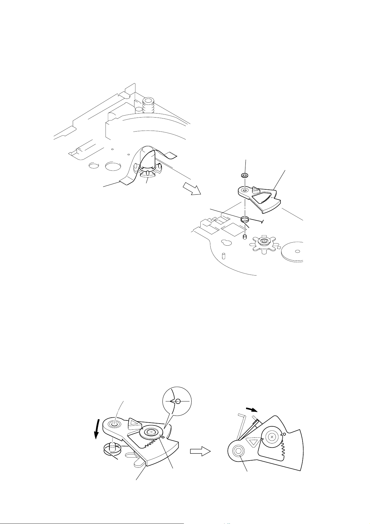
DISC LOCK ARM SL
L
1 Apply sellotape to the disc lock SL ass’y as shown in
figure to prevent the disc lock from falling off while
removing the disc arm SL.
2 washer
3 disc lock arm S
sellotape
(Fig. F. 1)
disc lock SL ass’y
D lock spring SL
INSTALLING THE DISC LOCK ARM SL
POSITIONING OF THE DISC LOCK ARM SL IS REQUIRED. (Refer to Fig. F. 2)
(1) Place the disc lock spring SL as shown in the figure.
(2) Insert the disc lock pinion into the hole on the disc lock arm SL.
(3) Adjust the position of the disc lock arm SL until its mark meets
the V-cut of the disc lock pinion as shown in the figure.
(4) Insert the shaft hole of the disc lock arm SL into the shaft.
(5) Hook the end of the disc lock spring SL on the chassis hole as
shown in the figure.
(6) Reassemble the washer in place.
(7) Peel off the sellotape. Refer to Fig. F. 1.
disc lock arm SL
disc lock pinion
(Fig. F. 2)
washer
17
Page 18

STC POS GEAR SL
L
Note:DO NOT remove the STC POS Gear
SL together with the STC Motor SL Ass’y
(Stocker) (M3), always replace it alone.
If they are removed at the same time and
the gear in the stocker height becomes out
of position.
2 STC POS gear SL
1 washer
MA chassis SL S ass’y
POSITIONING OF THE STC POS GEAR SL REQUIRED
Note:Assemble the STC POS gear
SL so that the mark on the
STC POS gear SL meets the
b
mark on the MA chassis SL
S ass’y.
c
STC POS gear SL
b
c
LDG PLATE CAM SL
1 washer
2 LDG plate cam SL
Note:Never use nail when
turning the emergency
gear SL.Otherwise, the
gear tooth may be broken.
emergency gear SL
(Fig. G. 1)
INSTALLING THE LDG PLATE CAM SL
POSITIONING OF THE LDG PLATE CAM SL IS REQUIRED.
(1) Turn the emergency gear SL in the direction of the arrow as shown
in Fig. G. 1 until it stops.
(2) Assemble LDG plate cam SL so that the center of the LDG plate cam
SL, mark on the LDG plate cam SL and the center of the shaft are
aligned on one line as shown in Fig. G. 2.
(3) Turn the emergency gear SL in revers until the marks , on
LDG plate cam SL are almost aligened as shown in Fig. G. 3. (This
operation is required to return to the mechanism in standby state.)
d
e
d
(Fig. G. 2)
Note:Never use nail when
turning the emergency
gear SL.
Otherwise the gear
tooth may be broken.
emergency gear SL
d
d
LDG plate cam S
e
18
(Fig. G. 3)
Page 19

SECTION 4
V
ELECTRICAL ADJUSTMENT
Forcus Bias Adjustment
Note:
1. CD Block is basically designed to operate without adjustment.
2. Use YEDS-18 disc (3-702-101-01)
3. Use an oscilloscope with more than 10 MΩ impedance.
4. Clean the object lens by an applicator with lens cleaning liquid when the signal level is low than specified value with the
following adjustment.
5. Adjust the focus bias adjustment when optical block is replaced.
Focus Bias Adjustment
oscilloscope
(DC range)
MAIN R237 board
TP (RFO)
TP (VC)
+
–
Procedure :
1. Connect oscilloscope to TP101(pin 1: RFO) and TP101 (pin
3: VC) on MAIN R237 board.
2. Press the
I/1 button to turn the power on.
3. Put test disc (YEDS-18) in and press the u button to play-
back.
4. Adjust VR102 so that oscilloscope waveform is as shown in
the figure below. (eye pattern)
A good eye pattern means that the diamond shape ( ) in the
s
center of the waveform can be clearly distinguished.
5. After adjustment, check the RF signal level.
Adjustment Location:
– MAIN R237 BOARD (Conductor Side) –
TP101
(Pin 1 : RFO)
TP101
(Pin 3 : VC)
VR102
FOCUS BIAS
ADJUSTMENT
VOLT/DIV: 200 m
TIME/DIV: 500 ns
10: 1
level:
+0.3
1.0 Vp-p
- 0.2
19
Page 20

MEMO
20
Page 21

SECTION 5
TRA ASSY V619
MAIN R237 board
DIAGRAMS
5-1. NOTE FOR PRINTED WIRING BOARDS AND SCHEMATIC DIAGRAMS • Circuit Boards Location
Note on Printed Wiring Board:
• X : parts extracted from the component side.
• Y : parts extracted from the conductor side.
z
•
• b : Pattern from the side which enables seeing.
(The other layers' patterns are not indicated.)
Caution:
Pattern face side: Parts on the pattern face side seen from
(Conductor Side) the pattern face are indicated.
Parts face side: Parts on the par ts face side seen from
(Component Side) the parts face are indicated.
: Through hole.
Note on Schematic Diagram:
• All capacitors are in µF unless otherwise noted. pF: µµF
50 WV or less are not indicated except for electrolytics
and tantalums.
• All resistors are in Ω and 1/
specified.
• 2 : nonflammable resistor.
• C : panel designation.
Note:
The components identified by mark 0 or dotted
line with mark 0 are critical for safety.
Replace only with part
number specified.
• U : B+ Line.
• V : B– Line.
• H : adjustment for repair.
• V oltages are taken with a VOM (Input impedance 10 MΩ).
Voltage variations may be noted due to normal production tolerances.
• Waveforms are taken with a oscilloscope.
Voltage variations may be noted due to normal production tolerances.
• Circled numbers refer to waveforms.
• Signal path.
F : TUNER (FM/AM)
J : CD PLAY
E : TAPE
4
W or less unless otherwise
Note:
Les composants identifiés par
une marque 0 sont critiques
pour la sécurité.
Ne les remplacer que par une
pièce portant le numéro
spécifié.
POWER SW board
FRONT board
TACT SW board
DOOR SW board
MAIN board
TUNER (FM/AM)
RELAY board
JACK board
PHOTO JACK board
AMP board
POWER SUPPLY board
AC board
2121
Page 22

HCD-LS1
5-2. PRINTED WIRING BOARD – CD Section –• See page 21 for Circuit Boards Location.
1
2 3 4 5 6 7 8 9 10 11 12 13 14 15
(Page 26) (Page 30) (Page 26)
A
MAIN R237 BOARD
B
C
D
Q403
E
(COMPONENT SIDE)
BCE
16
9
U502
18
Q414
ECB
Q404
D802
R401
R423
C423
C406
+
C405
A/K
A
K
(CONDUCTOR SIDE)
ZD405
ZD404
C407
+
C403
+
D409
Q521
Q522
ZD401
KKA
BCE
BCE
R553
D521
R563R554
R552
AKK
R402
R403
ZD521
Q8012
R551
L802
AKK
BCE BCE
C402
D801
Q8011
J404
R404
D404
1
CP503
Q412
BCE
C414
R414
BCE
R408
R407
KKA
Q413
AKK
R526
D517
R565
R564
R8102
R8101
3
R409
R530
ZD502
ZD503
R410
C509
R406
D401
R531
KA
Q502
L401
L402
1
R532
C413
D516
KKA
R527
R528
R415
BCE
CP501
R405
BCE
R416
C505
R519
R529
Q411
C506
R516
C411
7
R518
B
C
Q501
E
R517
+
MAIN R237 BOARD
4
1
U401
C404
ECB
R417
R411
C422
R412
BCE
Q402
ECB
Q401
R418
R419
R413
ZD402
1
5
TP101
FOR
ADJUSTMENT
A D B C
(Page 26)
1
5
CP502
D406
AKK
+
C409
R420
+
C417
R422
C401
C419
+
ZD403
R524
C504
(CHASSIS)
R603R602
C
R708
C134
R114
C123
C157
R713
C122
R704
R17
+
C141
R573
R572
R571
R570
R8082
R8092
C8102
+
R8091
R8081
R543
R510
R548
R511
R542
R508
R541
R509
R540
R512
R539
R513
C164C140
R538
R549
R537
R506
R536
R507
+
C8101
Q102Q103
E
BCE
B
R700
R199
R707
R703
R115
R116
C121
C112
R711
R702
R125
R126
R121
R122 R123
C114
R177
C106
C115 R110
R111
C116
R143
C101
R145
R144
C105
R142
R141
C1041
C1042
C145
C144
R120
R132
C142
R136
R134
C136C138
+
R124
R14
C135
R13
R12
R11
R135
R10
X501
C11
R19
R18
C12
R4R5R6
L503
C5072
C5071
C521
C516
R3
R2
R9
C143
R105
VR102
R102
R181
R137
R103
C107
R200
C1092
C1091
C110
C1112
R106
R127 R158
C137
R195
R194
C165
R196
R159
C1111
C169
R545
R131
C139
R129
R130
R133
C1
R109
C103
KKA
D101
R101
+
L101
C102
R706
R179
R180
C113
F
CP103
122
G
10
U107
516
H
I
J
40 21
41
60
61 80
K
05
L
516
516
U106
U501
10
10
U105
1
8
U103
4
5
CP102
1
20
1
U404
14
28
15
TRA ASSY
18
V619
85
U180
14
16
CP101
1
Q101
BCE
253232
1
24
U101
17
8
169
OPTICAL PICK-UP
BLOCK
(KSS-540A)
20 1
21
U102
40
41 60
80
61
M4
(LOADING)
M
M
M
CD SENSOR
BLOCK
M5
(UP/DOWN)
M3
(STOCKER)
D102
C131 C130
C127
X101
R710
AK
+
C128
C133 R197
C132
R15
C126
C125
L102
C129
C117
R112
C118
C163
R147
+
R714
L103
+
R705
C8012 C8011
R139
C162
R709
C8022
R8012
R8022
R8032
R8031
R8021
R8011
C8021
R128C124
R117
R701
R119
C119
R113
R712
R118
C120
M M
M1
(SLED)
M2
(SPINDLE)
2222
Page 23

• Semiconductor
Location
Ref. No. Location
D101 J-12
D102 K-9
D401 B-12
D404 B-11
D406 E-15
D409 C-11
D516 B-13
D517 B-12
D521 D-11
D801 C-11
Q101 J-5
Q102 I-10
Q103 I-10
Q401 D-7
Q402 C-9
Q403 E-2
Q404 C-7
Q411 B-13
Q412 B-12
Q413 B-12
Q414 C-6
Q501 C-13
Q502 C-13
Q521 C-11
Q522 C-11
Q8011 C-11
Q8012 C-11
HCD-LS1
5-3. SCHEMATIC DIAGRAM – CD Section (1/3) –• See page 33 for Waveforms.
U101 K-5
U102 J-7
U103 I-7
U105 H-2
U106 H-2
U107 H-2
U180 J-4
U401 B-9
U404 J-3
U501 J-2
U502 C-3
ZD401 B-11
ZD402 D-9
ZD403 E-15
ZD404 D-10
ZD405 D-10
ZD502 C-12
ZD503 C-12
ZD521 B-11
(Page 24)
Note:
• In the printed wiring diagram of the MAIN R237
Board, “A and L” or “B and R” of the last code of Ref
No. on the silk-screen printing drawing of the main
unit are replace with “1” or “2” respectively.
Example: C104A → C1041
R801R → R8012
• Voltages and waveforms are dc with respect to ground
under no-signal conditions.
no mark : CD PLAY
The components identified by mark 0 or dotted
line with mark 0 are critical for safety.
2323
Replace only with part number specified.
Les composants identifiés par une marque 0 sont
critiques pour la sécurité. Ne les remplacer que
par une pièce portant le numéro spécifié.
Page 24

HCD-LS1
5-4. SCHEMATIC DIAGRAM – CD Section (2/3) –• See page 33 for Waveforms. • See page 36 for IC Block Diagram.
(Page 27)
(Page 27)
(Page 27)
(Page 23)
• Voltages and waveforms are dc with respect to ground
under no-signal conditions.
no mark : CD PLAY
(Page 25)
2424
Page 25

5-5. SCHEMATIC DIAGRAM – CD Section (3/3) –• See page 33 for Waveform.
HCD-LS1
(Page 24)
(Page 31)
• Voltages and waveforms are dc with respect to ground
under no-signal conditions.
2525
no mark : CD PLAY
Page 26

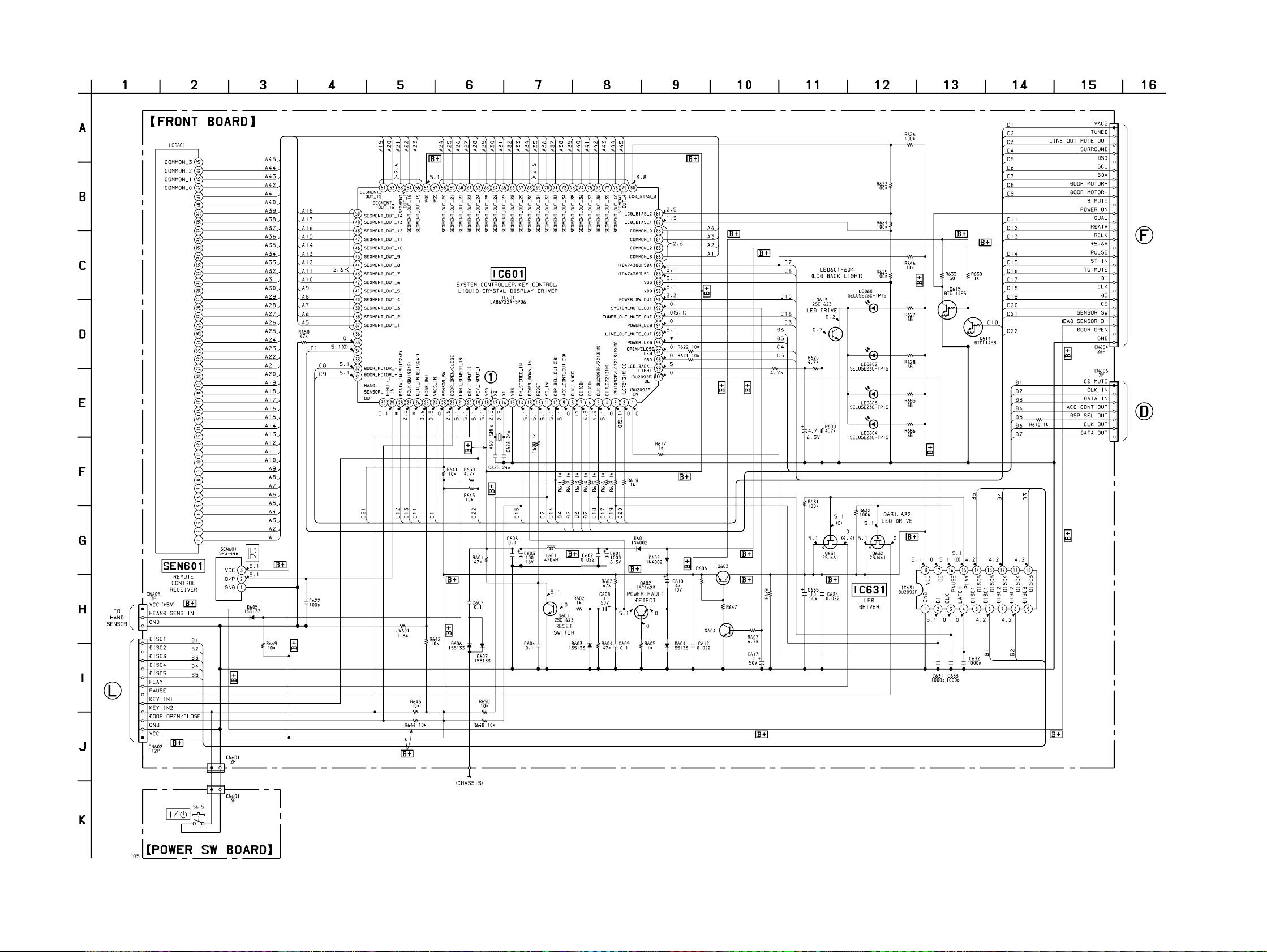
HCD-LS1
5-6. PRINTED WIRING BOARDS – MAIN Section –• See page 21 for Circuit Boards Location.
• Semiconductor
Location
Ref. No. Location
D200 F-2
D251 B-5
D252 B-4
D253 C-3
D254 B-4
D304 H-4
D312 C-3
D316 G-4
D321 D-2
D352 E-3
D391 B-2
IC103 C-8
IC201 D-8
IC251 C-5
IC321 E-6
IC351 F-4
IC390 B-6
IC391 C-7
PH200 E-2
Q201 C-4
Q202 D-4
Q203 C-5
Q204 D-5
Q205 D-3
Q301 G-6
Q302 G-6
Q303 G-6
Q304 F-9
Q305 G-4
Q306 H-8
Q311 G-7
Q312 G-7
Q313 G-8
Q316 G-4
Q317 G-3
Q321 E-5
Q351 E-4
Q352 E-4
Q371 G-6
Q372 F-6
Q373 G-7
Q374 F-7
Q375 G-6
Q376 G-5
Q377 G-5
Q381 F-8
Q382 F-7
Q383 G-8
Q384 G-8
A
B
C
D
E
F
G
H
1
(Page 30)
PH200
CD DIGITAL
OUT
(OPTICAL)
R2001
(R200A)
C2001
(C200A)
S391
1234 5
678910
F
E
(Page 28)
PHOTO JACK
PH200
B
(Page 22)
BOARD
CN204
C200
1
3
1
1-678-385-
05
1
2 3 4 5 6 7 8 9 10 11
MAIN BOARD
S392
PANEL
OPEN/CLOSE
D391
R399
CN604
26
25
(AEP, UK)
R145
R143
R144
D312
2
1
SDG
Q205
D321
1
2
CN204
2
D352
R200
D200
CN200
2
C355
C357
C359
11
C313 C316
C307
+
+
+
C306
12345
678910
PANEL OPEN
MANUAL AUTO ON/AUTO
D254
D253
C257
+
R258
C214
CN201
7
C201
1
R351
R355
R361
R353
5
R359
R357
8
C333
+ +
Q317
BCE
R316
Q305
S391
C251
+
R201
R257
C213
C202
BCE
Q351
IC351
BCE
D252 D251
R253
R251
R252
+
C252
R213
BCE
R209
Q201
R210
BCE
R214
Q202
R204
R203
R202
Q352
BCE
R356
R354
4
1
C334
Q316
BCE
R318
R317
D316
R307
C310 C309
D304
C253
R362
5
8
C205
R212R211
R360
+ +
C206
IC251
R215
C356
R358
C308
+
R306
R352
C358
C360
C256
C331
+
R216
C387
+
C220
R254
4
1
+
R217
R218
Q203
+
Q204
R325
R326
C329
BCE
C327
C328
C330
C392
R391
R328
R334
IC390
1
3
+
R392
R393
IC391
R394
1
C290
CN202
1
C255
+
R256
C207
R219
C209
++
C208
BCE
C325
R331R333
R220
Q321
C210
R223
C324
R329
C323
S
R327
IC321
4
5
1
8
R332
Q372
Q301Q303
1
CN203
BCE
R377
BCE
R373
R372
BCE
Q371
R371
Q302
7
2
Q376
R304
+
C389
Q377
C302
C301
R302
BCE
+
R380
R381
Q375
C388
R379
+
R225
+
C249
+
R376
R303
C391
6510
C203
R227
BCE
Q374
R375
CN301
R226
BCE
3
+
R228
R364
R382
R370
Q373
(AEP, UK)
+
C211
C212
R363
R369
C162
16 9
C163
X102
R321 R322
C321
C322
+ +
C204
28 15
IC103
18
C160
C158
+
C243
+
C240 C239
R235
R236
C241
C242
IC201
114
C216
C271
+ +
Q382
C215
C232
+
+
R281
C272
R221
R222
Q381
R282
C399
R237
R238
C381
C234
C103
C104
C382
+ +
+
BCE
C383
C367
R397
R366R365
BCE
+
CN303
R311
1
C386
BCE
Q312
+
R314
R308
R309
R312
C385
R315
BCE
Q311
BCE
R389R390
9
Q306
SDG
+
Q383
Q313
R313
R368R367
C384
+
+
R388R387
C159
C161
+
C157
+
R231
R233
R234
R232
R230
Q384
C368
1
R142
C231
C233
C235
C237
C238
C236
R229
Q304
BCE
C305
+
C326
+ +
CN302
1
L101
R305
C362
3
C312
+
2
CN391
CN101
2
14
(Page 22)
1
1
C102
15
A
AM
ANTENNA
FM
TUNER PACK (FM/AM)
(SUPPLIED WITH THE ASSEMBLED BLOCK)
75Ω
C
G J
(Page 22) (Page 34) (Page 28) (Page 34)
H
M391
(DOOR)
M
2626
Page 27

5-7. SCHEMATIC DIAGRAM – MAIN Section –• See page 33 for Waveform. • See page 36 for IC Block Diagram.
HCD-LS1
(Page
29)
(Page 24)
(Page 24)
(Page 24)
(Page 31)
(Page 35)
(Page 35)
• Voltages and waveforms are dc with respect to ground
under no-signal (detuned) conditions.
no mark : TUNER (FM/AM)
: Impossible to measure
∗
(Page 29)
The components identified by mark 0 or dotted
line with mark 0 are critical for safety.
2727
Replace only with part number specified.
Les composants identifiés par une marque 0 sont
critiques pour la sécurité. Ne les remplacer que
par une pièce portant le numéro spécifié.
Page 28

HCD-LS1
5-8. PRINTED WIRING BOARDS – AMP/RELAY/JACK Board –• See page 21 for Circuit Boards Location.
• Semiconductor
Location
Ref. No. Location
D201 F-9
D202 F-9
D203 F-9
D204 F-10
D205 E-8
D206 E-8
D501 F-1
D502 F-3
D503 F-1
D504 F-3
D505 G-5
D506 H-6
D507 H-6
D508 F-8
D509 F-9
D510 F-8
D511 F-9
D512 H-6
D513 H-6
D514 G-2
D515 G-2
D516 G-2
IC501 G-2
IC502 F-11
IC503 H-2
Q501 G-5
Q502 F-9
Q503 F-9
Q504 G-5
Q505 G-6
1
AMP BOARD
2 3 4 5 6 7 8 9 10 11
(COMPONENT SIDE)
RELAY BOARD
(COMPONENT SIDE)
A
C951
11
C952
22
C953
33
C954
B
44
C955
55
C959
9
8
7
6
C958
C957
C956
9
8
7
6
JACK BOARD
(COMPONENT SIDE)
C
D
(Page 26)
E
2
17
CN201
C206
C205
D202
JK201
TAPE OUT
D204
C203
JK202
TAPE IN
JK202
R513
3
1
R517
R514
R520
R522
R521 R519
12
2
R515
C555
C518
C518
C519
R553
C524
C531
CN505
61
+
R523
C553
54
IC502
8
1
R552
21
C530
+
+
C523
+
C556
+
R550
C554
R518
C520
R516
+
C547
C552
C526
R524
C548
+
1
2
3
D511
Q502
Q502, 503
1
2
3
CN503
RIGHT SPEAKER
C525
(CONDUCTOR SIDE)
54
623
C551
R527
PHONES
D203
Q503
JK501
JK201
3
1
C204
D201
1
2
R525
3
JK501
1
D509
D509
R526
+
C549
E
AMP BOARD
L503
D501
F
G
L506
C538
C512
C511
C517
D503
+
+
+
C508
H
05
(CONDUCTOR SIDE)
C505
L501
+
C550
IC501
D515
D516
C539
C537
D514
R507
R535
R533
C534C532
C542
32
C503
C514
C541
C501
+
C507
R502
L505
C513
R504R530
C502
C506
C504
C558
CN504
LEFT SPEAKER
(IMPEDANCE USE 4Ω)
+–
RELAY BOARD
C515
+
C557
C509
+
R503
R531
R529
C529
+
C510
D505
Q501
CN502
3
1
19
(CONDUCTOR SIDE)
RY501
Q504
R509
D513
D512
CN501
Q505
D507
R543
–2
–1
C527
C545
+
R510
R538
+
R549
R546
+
R548
C546
R551
D506
16
CN505
R545
C544
+
R544
C5021
(C502A)
2
C5011
(C501A)
2
1
1
R501
31
R505
8
5
C528
D504
R536
C543
+
R506
L504
D502
C540
R528
L502
+
C516
C535C533C536
R508
2
1
R532
R534
1
4
IC503
JACK BOARD
D206
D205
D508
D510
+
(IMPEDANCE USE 4Ω)
–
K J
(Page 34) (Page 26)
2828
Page 29

5-9. SCHEMATIC DIAGRAM – AMP/RELAY/JACK Board –
HCD-LS1
(Page
27)
(Page 35)
(Page 27)
• Voltages are dc with respect to ground under no-signal
(detuned) conditions.
no mark : TUNER (FM/AM)
The components identified by mark 0 or dotted
line with mark 0 are critical for safety.
2929
Replace only with part number specified.
Les composants identifiés par une marque 0 sont
critiques pour la sécurité. Ne les remplacer que
par une pièce portant le numéro spécifié.
Page 30
HCD-LS1
5-10. PRINTED WIRING BOARDS – PANEL Section (1/2) – • See page 21 for Circuit Boards Location.
• Semiconductor
Location
Ref. No. Location
D601 D-8
D602 D-8
D603 E-2
D604 D-2
D605 E-7
D606 E-4
D607 E-4
IC601 C-5
IC631 C-2
LED601 A-9
LED602 A-1
LED603 B-9
LED604 B-1
Q601 E-2
Q602 D-3
Q613 C-2
Q631 D-2
Q632 D-1
SEN601 C-9
1
A
FRONT BOARD
LED602
LED604
B
R686
Q613
C
CN602
SDG
D
Q632
C606
R644
R643
2 3 4 5 6 7 89
R628
BCE
121
R632
R645
D603
LED602, 604
(LCD BACK LIGHT)
L
R620
R609
C633
10
Q631
R631
SDG
(Page 32)
C632
IC631
R605
D604
Q602
C631
C634
19
18
BCE
R625
R607
C609
R626
R617
R603
LED601, 603
(LCD BACK LIGHT)
(Page 22)
45
LCD601
51
50
C608
+
R624 R623
C613
+
C610
R646
+
81
R622
80
R621
IC601
31
30
100
1
R619
R618
R616
R615
C625
C626
X601
C603
+
R659
L601
1
R641
C612
C601
C635
+
+
C602
JW601
D602
R650
R642
D601
D
1
R612
R613
CN604
1
SEN601
LR
LED601
LED603
CN606
R611
C622
R610
3
R614
R685
7
F
R627
1
(Page 26)
BCE
C604
R601
E
05
R602
R604
Q601
R608
POWER SW BOARD
S615
/
1-678-387-
CN601
CN601
1
2
1
2
11
(CHASSIS)
D606
D607
C607
R649
D605
CN605
3
TO HAND SENSOR
26
R648
1
R658
3030
Page 31
5-11. SCHEMATIC DIAGRAM – PANEL Section (1/2) –• See page 33 for Waveform. • See page 36 for IC Block Diagram.
HCD-LS1
(Page 27)
(Page
32)
(Page 25)
• Voltages and waveforms are dc with respect to ground
under no-signal (detuned) conditions.
no mark : TUNER (FM/AM)
3131
( ) : CD PLAY
: Impossible to measure
∗
Page 32

HCD-LS1
5-12. PRINTED WIRING BOARDS – PANEL Section (2/2) –• See page 21 for Circuit Boards Location.
1
A
TACT SW BOARD
B
S601
FUNCTION
S608
TUNER/BAND
C
CN602
L
D
05
(Page 30)
2 3 4 5 67
LED651, S602
LED656, S609
112
DOOR SW BOARD
DISC 1
R656
S691
DOOR
OPEN/CLOSE
R651
S601-614
LED651
AAK
AAK
S609
R657
LED656
R678
R671
CN603
R691
1-678-836-
LED652, S603
DISC 2
S610
R679
1
2
LED651-656
R652
R672
1
11
AAK
S603S602
CN603
LED652
2
LED653, S604
DISC 3
S611
TUNER –
R673
R653
R674
LED653
AAK
S604
R680
LED654, S605
R681
DISC 4
S612
TUNER +
R654
LED654
AAK
S605
LED655, S606
DISC 5
R675
R682
R676
R655
LED655
AAK
S606
S613
R683
R677
S614
VOLUME –
S607
VOLUME +
R684
5-13. SCHEMATIC DIAGRAM – PANEL Section (2/2) –
(Page 31)
• Semiconductor
Location
Ref. No. Location
LED651 B-3
LED652 B-4
LED653 B-4
LED654 B-5
LED655 B-6
LED656 C-3
3232
Page 33
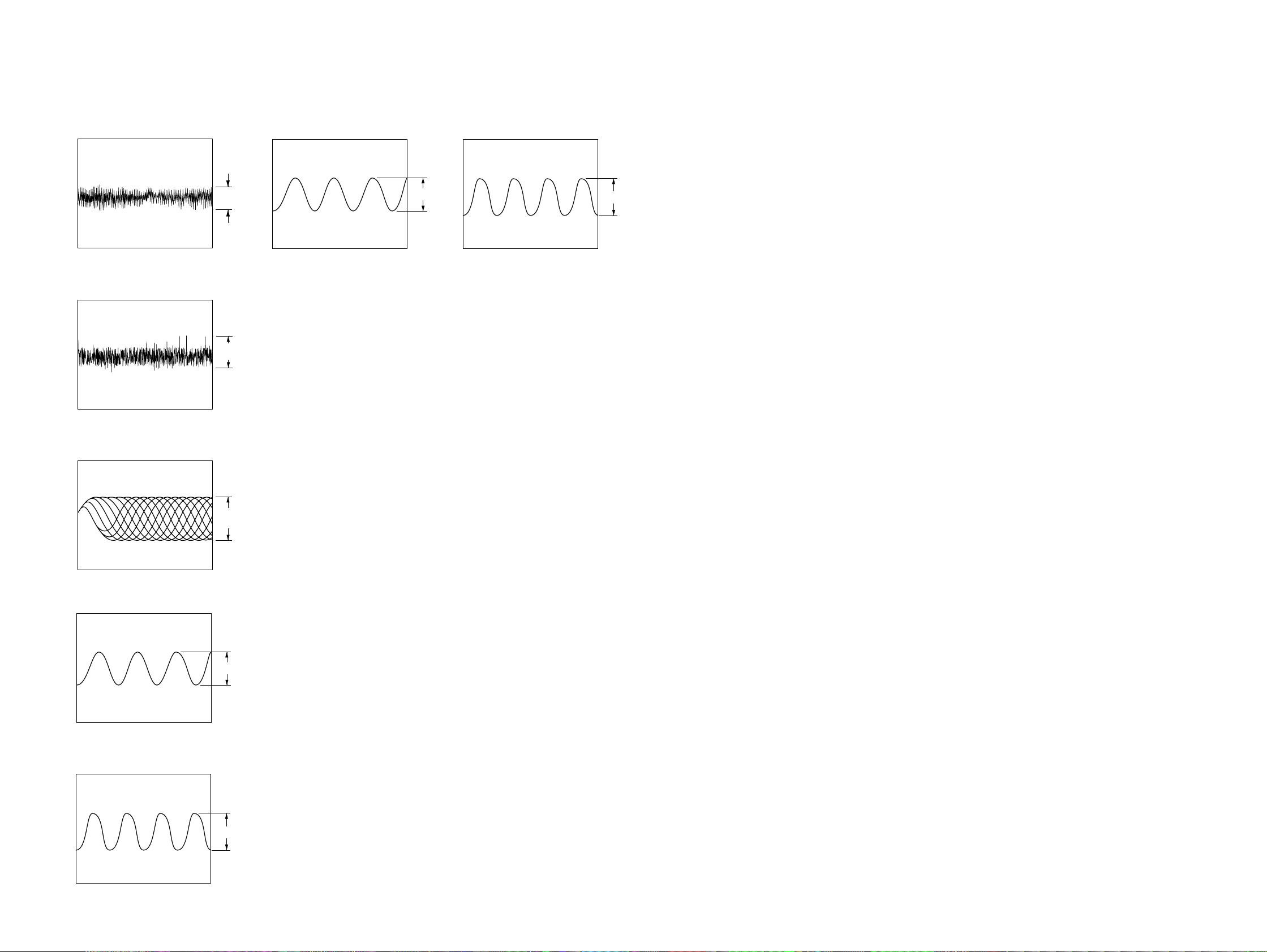
• Waveforms
– MAIN R237 Board –
– MAIN Board –
– FRONT Board –
1 U101 8 (TE), U102 ra (TE)
(CD Play Mode)
2 U101 q; (FE), U102 el (FE)
(CD Play Mode)
3 U101 wf (RFI), wg (RFO)
U102 rd (RFDC), ta (RFAC)
(CD Play Mode)
Approx.
140 m Vp-p
Approx.
200 mVp-p
1 IC103 qd (XI)
4.332 MHz
3.2 Vp-p
1 IC601 qj (X2)
5.2 Vp-p
5 MHz
4 U102 yh (XTAI)
16.9344 MHz
5 U501 yl (X2)
Approx.
1.2 Vp-p
2.4 Vp-p
3.7 Vp-p
4.194304 MHz
3333
Page 34

HCD-LS1
5-14. PRINTED WIRING BOARDS – POWER SUPPLY Section –• See page 21 for Circuit Boards Location.
• Semiconductor
Location
Ref. No. Location
D1 H-6
D2 H-6
D3 H-6
D4 H-6
D5 G-5
D6 F-4
D7 F-4
D8 G-4
D9 G-4
D10 E-6
D11 H-6
D12 H-5
D13 F-6
D14 F-6
D15 F-6
D16 F-8
IC1 G-5
IC2 G-6
IC3 G-6
IC4 G-6
IC5 G-9
Q1 H-6
Q2 H-5
Q3 H-5
Q4 G-7
Q5 F-8
Q6 E-8
Q7 F-8
1
2 3 4 5 6 7 8 9
POWER SUPPLY BOARD
(COMPONENT SIDE)
A
B
C
AC BOARD
(COMPONENT SIDE)
D
1-678-395-
11
(Page 26) (Page 26) (Page 28)
T901
1
C9
42
IC1
R3
FB1
R5
D12
(CONDUCTOR SIDE)
D10
C13
1234
1234
5
D5
R1
Q3
C20
R17
R15
TH1
C28
R9
C12
R22
IC2 IC4
R16
D11
Q1
D3
D1
Q2
D4
D14
D2
R14
R10
IC3
3
1
+
C15
D15
D13
C27
R11
C18
R13
R12
C21
R4
C2
L2
C24
R30
+
R26
R27
GND1
+
Q4
2
3
L1
LINE
FILTER
1
4
+
C22
7
C16
+
+
C17
C5
C4
C3
CN1
Q6
R23
D16
L4
Q7
R24
R28
10
(CHASSIS)
2
1
Q5
C26
C30
1
L3
R25
C1
E
AC BOARD
(CONDUCTOR SIDE)
1
F501
2
1-678-395-
11
F
AC IN
G
POWER SUPPLY BOARD
5
6
C31
DC/DC CONVERTER
D6
D7
R6
R8
C10
C11
R7
C8
+
D9
D8
R2
+
C6
H
05
CN3
IC5
KHG
+
C23
3
1
CN2
R29
3
1
+
+
+
C25
1
+
C29
3434
Page 35

5-15. SCHEMATIC DIAGRAM – POWER SUPPLY Section –• See page 36 for IC Block Diagram.
HCD-LS1
(Page 29)
(Page 27)
(Page 27)
• Voltages are dc with respect to ground under no-signal
(detuned) conditions.
no mark : TUNER (FM/AM)
The components identified by mark 0 or dotted
line with mark 0 are critical for safety.
3535
Replace only with part number specified.
: Impossible to measure
∗
Les composants identifiés par une marque 0 sont
critiques pour la sécurité. Ne les remplacer que
par une pièce portant le numéro spécifié.
Page 36

• IC Block Diagrams
– MAIN R237 Board –
U102 CXD2587Q
– MAIN Board –
IC103 BU1924F (AEP, UK models)
RCLK
NC
VDD2
XO
141516 13 121110 9
VSS2
XI
T1
T2
LRCK
PCMD
BCK
EMPH
XVDD
XTAI
XTAO
XVSS
AVDD1
AOUT1
AIN1
LOUT1
AVSS1
AVSS2
LOUT2
AIN2
AOUT2
AVDD2
RMUT
LMUT
VDD
AVDD3
DOUT
60
DIGITAL
OUT
61
62
63
64
65
66
67
68
69
70
71
72
73
74
75
76
77
78
79
80
D/A
INTERFACE
TIMING
LOGIC
OVER SAMPLING
PWM
3rd ORDER
NOISE SHAPER
DIGITAL FILTER
SERIAL IN
INTERFACE
59
58
INTERNAL BUS
PWM
VSS
57
ERROR
CORRECTOR
16K
RAM
SUBCODE
PROCESSOR
FILO
FILI
PCO
54
56
55
53
DIGITAL
PLL
EFM
DEMODULATOR
SERVO
INTERFACE
SERVO AUTO
SEQUENCER
CLTV
AVSS3
52
ASYI
BIAS
RFAC
51
49
50
ASYMMETRY
CORRECTION
48
ASYO
47
AVDD0
46
IGEN
AVSS0
45
ADIO
44
SERVO DSP
FOCUS
SERVO
TRACKING
SERVO
SLED
SERVO
CE
TE
RFDC
43
41
42
OPERATIONAL
AMPLIFIER
ANALOG SWITCH
A/D
CONVERTER
PWM GENERATOR
CLOCK
GENERATOR
FOCUS PWM
GENERATOR
TRACKING
PWM GENERATOR
SLED PWM
GENERATOR
DIGITAL
CLV
MIRR, DFCT,
FOK
DETECTOR
SE
40
FE
39
VC
38
PLL
1187.5Hz
BIPHASE
DECODER
DEFFERENTIAL
XTSL
37
TES1
36
TEST
35
VSS
34
33
FRDR
32
FFDR
TRDR
31
TFDR
30
SRDR
29
28
SFDR
SSTP
27
MDP
26
25
LOCK
FOK
24
DFCT
23
22
MIRR
– FRONT Board –
IC631 BU2092F-E2
DECODER
1 43 65 872
QUAL
RDAT
COMPARATOR
8th SWITCHED
ANTI-ALIASING
VREF
PLL 57kHz
RDS/ARI
CAPACITOR
FILTER
FILTER
MUX
CLOCK
ANALOG
VDD1
VSS1
VSS3
CMP
TEST
DIGITAL
– POWER SUPPLY Board –
IC5 LA5617
1
2
SQSO
SQCK
3
XRST
4
SYSM
CPU
INTERFACE
7
5
6
XLAT
DATA
CLOK
8
SENS
9
10
SCLK
11 12
VDD
ATSK
13
SPOA
14
SPOB
1516171819
XUGF
XPCK
XLON
WFCK
GFS
20
C2PO
SCOR
12 BIT
SHIFT
REGISTER
12 BIT
STORAGE
REGISTER
LCK
VDDOEQ11
COUT
21
CONTROL
CIRCUIT
2 3
DATA
4
CLOCK
1
VSS
16 15 14 13 12
1718
Q10Q9Q8Q7Q6
OUTPUT
BUFFER
(OPEN DRAIN)
5 6 7 8 9
Q2
Q1
Q0
Q5
10
11
ERROR
Q4
Q3
AMP
2 3
1
VO1
VCC
ON/OFF
VREF
CN1
CURRENT
LIMITER
VMUTE VCC
VCC
4
EN
CURRENT
LIMITER
5 6 7 8 9
GND
EN DISPLAY
ON/OFF
140uA
~_
COMPARATER
VREF
~_
1.8V
NC
CN2
ERROR
AMP
OVER HEAT
START
CIRCUIT
VREF
PROTECT
VEE
10
VO2
3636
Page 37

d
SECTION 6
EXPLODED VIEWS
NOTE:
• -XX and -X mean standardized parts, so they
may have some difference from the original
one.
• Color Indication of Appearance Parts
Example:
KNOB, BALANCE (WHITE) . . . (RED)
↑↑
Parts Color Cabinet's Color
(1) MAIN CASE SECTION
not supplied
7
6
5
4
#6
3
2
• Items marked “*” are not stocked since they
are seldom required for routine service. Some
delay should be anticipated when ordering
these items.
• The mechanical parts with no reference number in the exploded views are not supplied.
• Hardware (# mark) list is given in the last of
the electrical parts list.
not
supplied
10
8
16
#2
9
not
supplied
11
14
12
#3
24
28
26
27
A
4
#6
29
#1
D704
13
25
#1
#2
21
23
12
D703
not
supplied
not supplied
D702
not supplied
22
The components identified by
mark 0 or dotted line with mark
0 are critical for safety.
Replace only with part number
specified.
Les composants identifiés par une
marque 0 sont critiquens pour la
sécurité.
Ne les remplacer que par une pièce
portant le numéro spécifié.
D701
not supplie
not supplied
17
#1
#4
18
19
20
21
#1
#2
#6
30
31
1
not
supplied
Ref. No. Part No. Description Remark
1 X-4953-040-1 SLIDE DOOR ASSY
2 4-229-209-01 FUNCTION PANEL
3 4-229-217-01 MAIN CASE
4 4-229-220-01 SP. SCREW
5 4-229-208-01 FRONT WINDOW
6 4-229-214-01 FRONT SCREW
7 4-229-216-01 AL PANEL
8 4-229-219-01 POWER BUTTON (SUB)
9 PCB BRACKET
10 1-678-387-11 POWER SW BOARD
11 8-719-070-85 HAND SENSOR KU381-40
12 4-229-242-01 SP. HOOK BKT.
13 4-229-201-01 +B 2X8 SCREW
14 1-792-759-11 FFC (12CORE)
16 A-4473-557-A FRONT BOARD, COMPLETE
17 1-792-758-11 FFC (26CORE)
18 A-4473-559-A TACT SW BOARD, COMPLETE
19 FIBER WASHER
20 X-4953-039-1 FUNCTION BUTTON ASSY
A
33
32
Ref. No. Part No. Description Remark
21 LIGHT LEAK SEAL A
22 LIGHT LEAK SEAL B
23 4-229-330-01 SHEET METAL, EARTH
24 4-229-227-01 COIL SPRING
25 4-229-241-01 SCREW (2.6X6), TAPPING
26 DOOR SPRING
27 4-229-240-01 SLIDE DOOR WASHER
28 SLIDE DOOR CUSHION
29 1-678-386-11 DOOR SW BOARD
30 4-229-226-01 WORM GEAR HOLDER
31 4-229-222-01 WORM GEAR
32 X-4953-041-1 GEAR ASSY
33 4-229-264-01 BELT
34 4-229-259-01 BOTTOM COVER
D701 8-719-991-33 DIODE 1SS133T-77
D702 8-719-991-33 DIODE 1SS133T-77
D703 8-719-991-33 DIODE 1SS133T-77
D704 8-719-991-33 DIODE 1SS133T-77
34
#5
37
Page 38

(2) BOTTOM CASE SECTION
not
supplied
#19
D707
D708
not
supplied
#7
D801
51
not
supplied
52
#19
56
51
not
supplied
#1
57
#7
B
60
D706
#1
61
not supplied
D705
not supplied
59
#1
58
62
#8
#9
65
#19
#6
63
64
#18
66
B
#8
#19
not supplied
55
#20
#19
54
53
not supplied
#19
not supplied
Ref. No. Part No. Description Remark
51 4-229-265-01 MECHA, HOLDER
52 A-4473-561-A MAIN BOARD, COMPLETE
53 1-500-386-11 FILTER, CLAMP (FERRITE CORE)
54 4-229-328-01 EGG TERMINAL
55 1-678-395-11 AC BOARD
68
67
M391
not
supplied
not
supplied
Ref. No. Part No. Description Remark
63 4-229-260-01 SLIDE KNOB
64 SLIDE KNOB PLATE
65 A-4473-562-A PHOTO JACK BOARD, COMPLETE
66 4-229-258-01 BOTTOM CASE
67 1-792-757-11 AC CORD (POWER)
#2
#13
not supplied
not supplied
56 A-4473-563-A POWER SUPPLY BOARD, COMPLETE
57 A-4473-565-A RELAY BOARD, COMPLETE
58 A-4473-564-A AMP BOARD, COMPLETE
59 A-4473-566-A JACK BOARD, COMPLETE
60 FFC (15CORE)
61 1-693-473-21 TUNER PACK (FM/AM)
62 X-4953-038-1 TOP PANEL ASSY
38
68 4-229-263-01 AC CORD STOPPER
D705 8-719-991-33 DIODE 1SS133T-77
D706 8-719-991-33 DIODE 1SS133T-77
D707 8-719-991-33 DIODE 1SS133T-77
D708 8-719-991-33 DIODE 1SS133T-77
D801 8-719-070-85 DIODE KU381-4
M391 X-4953-037-1 MOTOR PULLEY ASSY (DOOR)
Page 39

109
Loading MF ass’y
107
107
C
D
Motor chassis
SL ass’y
Traverse mecha
ass’y
108
108
107
104
106
#12
104
105
#11
104
103
104
110
111
112
113
115
114
107
116
111
117
118
111
119
120
121
122
F
M3
123
#13
124
122
125
126
120
119
111
118
#14
F
E
127
129
130
111
128
#15
136
131
132
135
#11
134
107
133
#10
#10
#10
137
101
102
#11
#11
#11
C
E
D
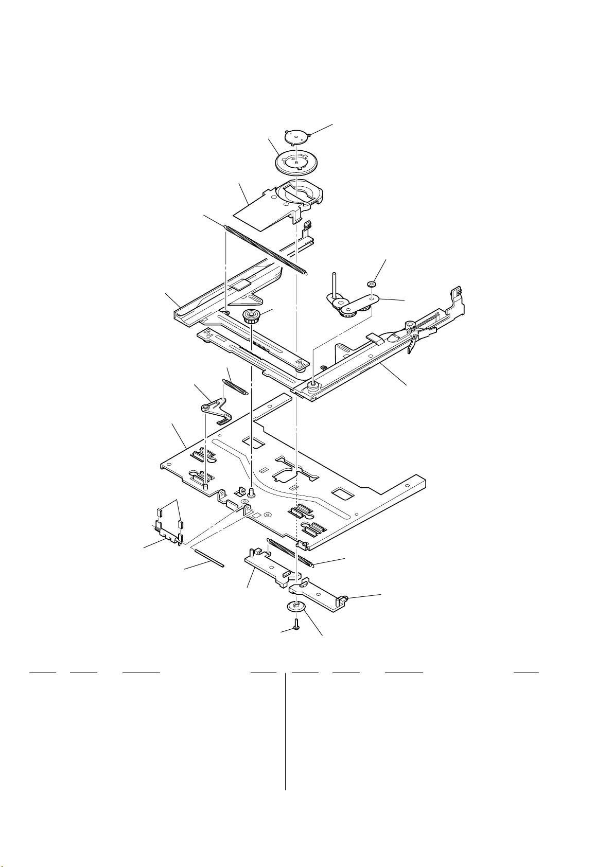
(3) MECHANISM DECK SECTION-1
(HG-1: MAIN SECTION)
120 STC SCREW NUT A SL
121 4-229-320-01 STC SPRING B SL
122 4-229-317-01 STC SP CAP A SL
123 STOCKER CD SL
124 4-229-316-01 STC SP CAP B SL
125 4-229-319-01 STC SPRING A SL
126 4-229-321-01 STC SPRING C SL
127 4-229-282-01 MA CHASSIS SL S ASSY
128 4-229-351-01 HEAT SINK REG
129 4-229-289-01 D LOCK SPRING SL
130 4-229-288-01 DISC LOCK ARM SL
131 4-229-326-01 WASHER
132 4-229-322-01 UD LINK ARM SL
133 4-229-323-01 PLATE SPRING SL
134 4-229-290-01 UD S CAM GUIDE SL
135 4-229-313-01 FR CHASSIS SL ASSY
136 A-4473-555-A MAIN R237 BOARD, COMPLETE
137 4-229-349-01 BOTTOM COVER MF ASSY
M3 4-229-284-01 STC MOTOR SL ASSY (STOCKER)
Ref. No. Part No. Description Remark Ref. No. Part No. Description Remark
101 4-229-348-01 F PANEL ASSY R237
102 4-229-314-01 PCB FLEX MECHA ASSY
103 4-229-318-01 MECH UD SUB CAM SL
104 4-229-315-01 PET WASHER
105 4-229-312-01 SUS BASE X SUB ASSY
106 4-229-324-01 ANTI RATTLE SP SL
107 4-229-295-01 SCREW 2.6X3
108 4-229-325-01 DAMPER SCREW SL
109 4-229-350-01 TOP COVER HS ASSY
110 4-229-327-01 DUST SEAL EMA SL
111 4-229-311-01 WASHER
112 4-229-287-01 STC POS GEAR SL
113 4-229-293-01 STC MOTOR SHEET SL
114 4-229-294-01 WASHER
115 4-229-291-01 STC WORM GEAR SL
116 4-229-286-01 STC C IDLE GEAR SL
117 4-229-283-01 DISC LOCK SL ASSY
118 4-229-292-01 STC IDLE GEAR SL
119 STC SCREW GEAR SL
39
Page 40

(4) MECHANISM DECK SECTION-2
(HG-1: MOTOR CHASSIS SL ASS’Y)
M5
152
153
155
153
154
159
#13
152
157
158
156
162
160
#16
161
163
164
165
M4
151
Ref. No. Part No. Description Remark Ref. No. Part No. Description Remark
151 4-229-306-01 EMERGENCY GEAR SL
152 4-229-308-01 BRACKET SCREW SL
153 4-229-311-01 WASHER
154 4-229-301-01 MECHA UD GEAR SL
155 4-229-305-01 LDG PLATE CAM SL
156 4-229-307-01 UD WORM PLATE SL
157 4-229-310-01 E-RING
158 4-229-300-01 UD WORM GEAR SL
159 4-229-302-01 MEC SENSOR RING SL
160 4-229-303-01 LDG WORM GEAR SL
161 4-229-304-01 LDG SENSOR RING SL
162 UD CAM GUIDE SL
163 4-229-299-01 UD CAM SL
164 4-229-309-01 UD CAM GUIDE W SL
165 4-229-296-01 MO CHASSIS SL S ASSY
M4 4-229-297-01 LDG MOTOR SL ASSY (LOADING)
M5 4-229-298-01 UD MOTOR SL ASSY (UP/DOWN)
40
Page 41

(5) MECHANISM DECK SECTION-3
(HG-1: TRAVERSE MECHA ASS’Y)
204
207
206
205
M1
206
206
208
#12
209
204
M2
203
#17
202
#12
214
201
214
Ref. No. Part No. Description Remark
201 4-229-268-01 TRA ASSY V619
202 1-792-692-11 WIRE FLEXIBLE BOARD
203 4-229-276-01 FIRST GEAR
204 4-229-273-01 DAMPER S SL
205 4-229-278-01 THIRD GEAR
210
#13
211
215
#13
212
213
The components identified by
mark 0 or dotted line with
mark 0 are critical for safety .
Replace only with part number specified.
Ref. No. Part No. Description Remark
209 4-229-280-01 SCREW 2X4
210 4-229-275-01 PU G PLATE H SL
211 4-229-279-01 RACK CA
0 212 1-251-883-11 OPTICAL PICK-UP KSS-540A
213 1-678-133-11 PICK-UP FLEXIBLE BOARD
Les composants identifiés par une
marque 0 sont critiques pour la
sécurité.
Ne les remplacer que par une pièce
portant le numéro spécifié.
206 4-229-294-01 WASHER
207 4-229-277-01 SECOND GEAR
208 4-229-272-01 POWER GEAR
214 4-229-271-01 SH LOCK PLATE SL
215 4-229-270-01 PU GUIDE SHAFT SL
M1 1-763-519-11 MOTOR (SLED)
M2 4-229-269-01 DISC MOTOR CH ASSY (SPINDLE)
41
Page 42
(6) MECHANISM DECK SECTION-4
(HG-1: LOADING MF ASS’Y)
259
262
261
260
263
252
258
254
253
251
255
256
257
264
265
266
270
269
Ref. No. Part No. Description Remark Ref. No. Part No. Description Remark
251 4-229-188-01 SHUT ARM SHAFT SL
252 4-229-193-01 SHUTTER ARM SL
253 4-229-187-01 SHUT ARM CUSH SL
254 LOADING CHASSIS SL ASSY
255 4-229-196-01 SHUTTER LEVER SL
256 4-229-192-01 SHUTTER SPRING SL
257 4-229-191-01 LDG CENTER GEAR SL
258 4-229-183-01 LOADING L MF ASSY
259 4-229-190-01 LDG RETURN SP SL
260 4-229-197-01 DISC G UPPER SL
268
261 4-229-200-01 DISC CRAMP BASE
262 4-229-198-01 STEEL RING
263 4-229-294-01 WASHER
264 4-229-185-01 LDG LINK SL ASSY
265 4-229-184-01 LOADING R MF ASSY
266 4-229-189-01 CLAMPER RE SP SL
267 4-229-195-01 CLAMP HOLDER L SL
268 4-229-199-01 CLAMP TOP
269 4-229-186-01 BT 1.7X5 +PAN (0 TYPE 3)
270 4-229-194-01 CLAMP HOLDER R SL
267
42
Page 43

SECTION 7
ELECTRICAL PARTS LIST
AC AMP
NOTE:
• Due to standardization, replacements in the
parts list may be different from the parts specified in the diagrams or the components used
on the set.
• -XX and -X mean standardized parts, so they
may have some difference from the original
one.
• RESISTORS
All resistors are in ohms.
METAL: Metal-film resistor.
METAL OXIDE: Metal oxide-film resistor.
F: nonflammable
Ref. No. Part No. Description Remark Ref. No. Part No. Description Remark
1-678-395-11 AC BOARD
*********
4-229-206-01 TERMINAL PIN (K)
4-229-207-01 TERMINAL PIN (L)
1-576-450-11 FUSE HOLDER
< FUSE >
0 F501 1-532-465-31 FUSE (3.15A/250V)
**************************************************************
A-4473-564-A AMP BOARD, COMPLETE
********************
4-229-344-01 SCREW (3X1), TAPPING
4-229-345-01 INSULATING SHEET (A)
4-229-346-01 INSULATING SHEET (B)
< CAPACITOR >
• Items marked “*” are not stocked since they
are seldom required for routine service.
Some delay should be anticipated when ordering these items.
• SEMICONDUCTORS
In each case, u: µ, for example:
uA. . : µA. . uPA. . : µPA. .
uPB. . : µPB. . uPC. . : µPC. .
uPD. . : µPD. .
• CAPACITORS
uF: µF
• COILS
uH: µH
C539 1-136-169-00 MYLAR 0.22uF 5% 50V
C540 1-136-169-00 MYLAR 0.22uF 5% 50V
C541 1-163-038-00 CERAMIC CHIP 0.1uF 25V
C542 1-163-038-00 CERAMIC CHIP 0.1uF 25V
C543 1-126-933-11 ELECT 100uF 20% 16V
C550 1-124-724-11 ELECT 47uF 20% 16V
C557 1-137-505-11 MYLAR 220PF 5% 50V
C558 1-137-505-11 MYLAR 220PF 5% 50V
C591 1-135-838-11 CERAMIC 2000PF
C592 1-135-838-11 CERAMIC 2000PF
C593 1-135-838-11 CERAMIC 2000PF
C594 1-135-838-11 CERAMIC 2000PF
C595 1-135-838-11 CERAMIC 2000PF
C596 1-135-838-11 CERAMIC 2000PF
C597 1-135-838-11 CERAMIC 2000PF
C598 1-135-838-11 CERAMIC 2000PF
C599 1-135-838-11 CERAMIC 2000PF
The components identified by
mark 0 or dotted line with mark
0 are critical for safety.
Replace only with part number
specified.
Les composants identifiés par une
marque 0 sont critiquens pour la
sécurité.
Ne les remplacer que par une pièce
portant le numéro spécifié.
When indicating parts by reference
number, please include the board.
C501 1-136-165-00 MYLAR 0.1uF 5% 50V
C502 1-136-165-00 MYLAR 0.1uF 5% 50V
C503 1-136-846-11 MYLAR 1.5uF 5% 50V
C504 1-136-846-11 MYLAR 1.5uF 5% 50V
C505 1-136-846-11 MYLAR 1.5uF 5% 50V
C506 1-136-846-11 MYLAR 1.5uF 5% 50V
C507 1-126-012-11 ELECT 470uF 20% 16V
C508 1-126-012-11 ELECT 470uF 20% 16V
C509 1-126-044-11 ELECT 1uF 20% 50V
C510 1-126-044-11 ELECT 1uF 20% 50V
C511 1-126-052-11 ELECT 100uF 20% 16V
C512 1-126-052-11 ELECT 100uF 20% 16V
C513 1-136-177-00 MYLAR 1uF 5% 50V
C514 1-136-165-00 MYLAR 0.1uF 5% 50V
C515 1-124-360-00 ELECT 1000uF 20% 16V
C516 1-124-360-00 ELECT 1000uF 20% 16V
C517 1-136-177-00 MYLAR 1uF 5% 50V
C528 1-136-165-00 MYLAR 0.1uF 5% 50V
C529 1-136-165-00 MYLAR 0.1uF 5% 50V
C532 1-163-038-00 CERAMIC CHIP 0.1uF 25V
C533 1-163-038-00 CERAMIC CHIP 0.1uF 25V
C534 1-163-038-00 CERAMIC CHIP 0.1uF 25V
C535 1-163-038-00 CERAMIC CHIP 0.1uF 25V
C536 1-163-038-00 CERAMIC CHIP 0.1uF 25V
C537 1-136-169-00 MYLAR 0.22uF 5% 50V
C538 1-136-169-00 MYLAR 0.22uF 5% 50V
< DIODE >
D501 8-719-210-21 DIODE 11EQS04
D502 8-719-210-21 DIODE 11EQS04
D503 8-719-210-21 DIODE 11EQS04
D504 8-719-210-21 DIODE 11EQS04
D514 8-719-820-58 DIODE 1SS177
D515 8-719-820-58 DIODE 1SS177
D516 8-719-820-58 DIODE 1SS177
< IC >
IC501 8-759-638-11 IC TA2020-020
IC503 8-759-100-96 IC NJM4558M
< COIL >
L501 1-419-281-11 INDUCTOR 10uH
L502 1-419-281-11 INDUCTOR 10uH
L503 1-419-281-11 INDUCTOR 10uH
L504 1-419-281-11 INDUCTOR 10uH
L505 1-419-282-11 INDUCTOR 10uH
L506 1-410-509-11 INDUCTOR 10uH
< RESISTOR >
0 R501 1-215-857-11 METAL OXIDE 10 5% 1W F
0 R502 1-215-857-11 METAL OXIDE 10 5% 1W F
R503 1-216-222-00 RES, CHIP 10K 5% 1/8W
43
Page 44

AMP DOOR SW FRONT
Ref. No. Part No. Description Remark
R504 1-216-222-00 RES, CHIP 10K 5% 1/8W
R505 1-216-230-00 RES, CHIP 22K 5% 1/8W
R506 1-216-230-00 RES, CHIP 22K 5% 1/8W
R507 1-216-220-00 RES, CHIP 8.2K 5% 1/8W
R508 1-216-246-00 RES, CHIP 100K 5% 1/8W
R528 1-216-270-00 RES, CHIP 1M 5% 1/8W
R529 1-216-270-00 RES, CHIP 1M 5% 1/8W
R530 1-216-270-00 RES, CHIP 1M 5% 1/8W
R531 1-216-270-00 RES, CHIP 1M 5% 1/8W
R532 1-216-262-00 RES, CHIP 470K 5% 1/8W
R533 1-216-262-00 RES, CHIP 470K 5% 1/8W
R534 1-216-262-00 RES, CHIP 470K 5% 1/8W
R535 1-216-262-00 RES, CHIP 470K 5% 1/8W
R536 1-216-174-00 RES, CHIP 100 5% 1/8W
**************************************************************
1-678-386-11 DOOR SW BOARD
***************
< RESISTOR >
R691 1-216-073-00 METAL CHIP 10K 5% 1/10W
< SWITCH >
Ref. No. Part No. Description Remark
< DIODE >
D601 8-719-200-02 DIODE 1N4002
D602 8-719-200-02 DIODE 1N4002
D603 8-719-991-33 DIODE 1SS133T-77
D604 8-719-991-33 DIODE 1SS133T-77
D605 8-719-991-33 DIODE 1SS133T-77
D606 8-719-991-33 DIODE 1SS133T-77
D607 8-719-991-33 DIODE 1SS133T-77
< IC >
IC601 8-759-677-45 IC LC867232A-5P06
IC631 8-759-396-78 IC BU2092F-E2
< RESISTOR >
JW601 1-216-053-00 METAL CHIP 1.5K 5% 1/10W
< COIL >
L601 1-419-636-11 COIL, CHOKE
< LIQUID CRYSTAL DISPLAY >
LCD601 1-804-047-11 LCD
S691 1-771-960-11 LEAF SW (DOOR OPEN/CLOSE)
**************************************************************
A-4473-557-A FRONT BOARD, COMPLETE
**********************
4-229-202-01 BACK LIGHT WINDOW
< CAPACITOR >
C601 1-126-916-11 ELECT 1000uF 20% 6.3V
C602 1-163-033-00 CERAMIC CHIP 0.022uF 50V
C603 1-125-972-91 ELECT 100uF 20% 16V
C604 1-163-038-00 CERAMIC CHIP 0.1uF 25V
C606 1-163-038-00 CERAMIC CHIP 0.1uF 25V
C607 1-163-038-00 CERAMIC CHIP 0.1uF 25V
C608 1-126-160-11 ELECT 1uF 20% 50V
C609 1-163-038-00 CERAMIC CHIP 0.1uF 25V
C610 1-124-589-11 ELECT 47uF 20% 16V
C612 1-163-033-00 CERAMIC CHIP 0.022uF 50V
C613 1-126-160-11 ELECT 1uF 20% 50V
C622 1-163-117-00 CERAMIC CHIP 100PF 5% 50V
C625 1-163-102-00 CERAMIC CHIP 24PF 5% 50V
C626 1-163-102-00 CERAMIC CHIP 24PF 5% 50V
C631 1-163-009-11 CERAMIC CHIP 0.001uF 10% 50V
C632 1-163-009-11 CERAMIC CHIP 0.001uF 10% 50V
C633 1-163-009-11 CERAMIC CHIP 0.001uF 10% 50V
C634 1-163-033-00 CERAMIC CHIP 0.022uF 50V
C635 1-124-247-91 ELECT 10uF 20% 35V
< CONNECTOR >
CN602 1-794-485-11 CONNECTOR 12P
CN604 1-794-484-11 CONNECTOR 26P
CN605 1-794-486-11 CONNECTOR 3P
< LED >
LED601 8-719-069-45 LED SELU5E23C-TP15 (LCD BACK LIGHT)
LED602 8-719-069-45 LED SELU5E23C-TP15 (LCD BACK LIGHT)
LED603 8-719-069-45 LED SELU5E23C-TP15 (LCD BACK LIGHT)
LED604 8-719-069-45 LED SELU5E23C-TP15 (LCD BACK LIGHT)
< TRANSISTOR >
Q601 8-729-120-28 TRANSISTOR 2SC1623-L6
Q602 8-729-120-28 TRANSISTOR 2SC1623-L6
Q613 8-729-120-28 TRANSISTOR 2SC1623-L6
Q614 8-729-029-66 TRANSISTOR DTC114ESA
Q615 8-729-029-66 TRANSISTOR DTC114ESA
Q631 8-729-052-45 FET 2SJ461
Q632 8-729-052-45 FET 2SJ461
< RESISTOR >
R601 1-216-089-00 RES, CHIP 47K 5% 1/10W
R602 1-216-049-11 RES, CHIP 1K 5% 1/10W
R603 1-216-089-00 RES, CHIP 47K 5% 1/10W
R604 1-216-089-00 RES, CHIP 47K 5% 1/10W
R605 1-216-049-11 RES, CHIP 1K 5% 1/10W
R607 1-216-065-00 RES, CHIP 4.7K 5% 1/10W
R608 1-216-049-11 RES, CHIP 1K 5% 1/10W
R609 1-216-065-00 RES, CHIP 4.7K 5% 1/10W
R610 1-216-049-11 RES, CHIP 1K 5% 1/10W
R611 1-216-049-11 RES, CHIP 1K 5% 1/10W
R612 1-216-049-11 RES, CHIP 1K 5% 1/10W
R613 1-216-049-11 RES, CHIP 1K 5% 1/10W
R614 1-216-049-11 RES, CHIP 1K 5% 1/10W
R615 1-249-049-11 CARBON 1K 5% 1/4W
R616 1-249-049-11 CARBON 1K 5% 1/4W
R617 1-216-049-11 RES, CHIP 1K 5% 1/10W
R618 1-249-049-11 CARBON 1K 5% 1/4W
R619 1-249-049-11 CARBON 1K 5% 1/4W
44
Page 45

FRONT JACK MAIN
Ref. No. Part No. Description Remark
R620 1-216-065-00 RES, CHIP 4.7K 5% 1/10W
R621 1-249-429-11 CARBON 10K 5% 1/4W
R622 1-249-429-11 CARBON 10K 5% 1/4W
R623 1-216-097-00 RES, CHIP 100K 5% 1/10W
R624 1-216-097-00 RES, CHIP 100K 5% 1/10W
R625 1-216-097-00 RES, CHIP 100K 5% 1/10W
R626 1-216-097-00 RES, CHIP 100K 5% 1/10W
R627 1-216-021-00 METAL CHIP 68 5% 1/10W
R628 1-216-021-00 METAL CHIP 68 5% 1/10W
R630 1-216-049-91 RES, CHIP 1K 5% 1/10W
R631 1-216-097-00 RES, CHIP 100K 5% 1/10W
R632 1-216-097-00 RES, CHIP 100K 5% 1/10W
R633 1-216-029-00 RES, CHIP 150 5% 1/10W
R641 1-216-073-00 METAL CHIP 10K 5% 1/10W
R642 1-216-073-00 METAL CHIP 10K 5% 1/10W
R643 1-216-073-00 METAL CHIP 10K 5% 1/10W
R644 1-216-073-00 METAL CHIP 10K 5% 1/10W
R645 1-216-073-00 METAL CHIP 10K 5% 1/10W
R646 1-216-073-00 METAL CHIP 10K 5% 1/10W
R648 1-216-073-00 METAL CHIP 10K 5% 1/10W
R649 1-216-073-00 METAL CHIP 10K 5% 1/10W
R650 1-216-073-00 METAL CHIP 10K 5% 1/10W
R658 1-216-065-00 RES, CHIP 4.7K 5% 1/10W
R659 1-216-089-00 RES, CHIP 47K 5% 1/10W
R685 1-216-045-00 METAL CHIP 680 5% 1/10W
R686 1-216-045-00 METAL CHIP 680 5% 1/10W
< IC >
SEN601 8-749-017-81 IC SPS-446 (REMOTE CONTROL RECEIVER)
< VIBRATOR >
X601 1-781-679-11 VIBRATOR, CRYSTAL (5MHz)
**************************************************************
A-4473-566-A JACK BOARD, COMPLETE
*********************
< CAPACITOR >
C203 1-163-038-00 CERAMIC CHIP 0.1uF 25V
C204 1-163-038-00 CERAMIC CHIP 0.1uF 25V
C205 1-163-038-00 CERAMIC CHIP 0.1uF 25V
C206 1-163-038-00 CERAMIC CHIP 0.1uF 25V
C518 1-128-526-11 ELECT 220uF 20% 10V
C519 1-163-009-11 CERAMIC CHIP 0.001uF 10% 50V
C520 1-163-009-11 CERAMIC CHIP 0.001uF 10% 50V
C523 1-126-868-11 ELECT 47uF 20% 50V
C524 1-126-868-11 ELECT 47uF 20% 50V
C525 1-163-009-11 CERAMIC CHIP 0.001uF 10% 50V
C526 1-163-009-11 CERAMIC CHIP 0.001uF 10% 50V
C530 1-104-942-11 ELECT 1uF 20% 50V
C531 1-104-942-11 ELECT 1uF 20% 50V
C547 1-128-526-11 ELECT 220uF 20% 10V
C548 1-126-163-11 ELECT 4.7uF 20% 50V
Ref. No. Part No. Description Remark
C554 1-163-129-00 CERAMIC CHIP 330PF 5% 50V
C555 1-163-133-00 CERAMIC CHIP 470PF 5% 50V
C556 1-163-133-00 CERAMIC CHIP 470PF 5% 50V
< DIODE >
D201 8-719-947-61 DIODE MTZJ-T-72-15B
D202 8-719-947-61 DIODE MTZJ-T-72-15B
D203 8-719-947-61 DIODE MTZJ-T-72-15B
D204 8-719-947-61 DIODE MTZJ-T-72-15B
D205 8-719-820-58 DIODE 1SS177
D206 8-719-820-58 DIODE 1SS177
D508 8-719-947-61 DIODE MTZJ-T-72-15B
D509 8-719-947-61 DIODE MTZJ-T-72-15B
D510 8-719-820-58 DIODE 1SS177
D511 8-719-820-58 DIODE 1SS177
< IC >
IC502 8-759-711-82 IC NJM4580E
< JACK >
JK201 1-563-281-41 JACK (TAPE OUT)
JK202 1-563-281-41 JACK (TAPE IN)
JK501 1-794-492-11 HP JACK (PHONES)
< TRANSISTOR >
Q502 8-729-231-55 TRANSISTOR 2SC2878-A
Q503 8-729-231-55 TRANSISTOR 2SC2878-A
< RESISTOR >
R511 1-216-138-00 RES, CHIP 3.3 5% 1/8W
R513 1-216-206-00 RES, CHIP 2.2K 5% 1/8W
R514 1-216-206-00 RES, CHIP 2.2K 5% 1/8W
R515 1-216-238-91 RES, CHIP 47K 5% 1/8W
R516 1-216-238-91 RES, CHIP 47K 5% 1/8W
R517 1-216-210-00 RES, CHIP 3.3K 5% 1/8W
R518 1-216-210-00 RES, CHIP 3.3K 5% 1/8W
R519 1-216-254-00 RES, CHIP 220K 5% 1/8W
R520 1-216-254-00 RES, CHIP 220K 5% 1/8W
R521 1-216-190-00 RES, CHIP 470 5% 1/8W
R522 1-216-190-00 RES, CHIP 470 5% 1/8W
R523 1-216-182-00 RES, CHIP 220 5% 1/8W
R524 1-216-150-00 RES, CHIP 10 5% 1/8W
R525 1-216-150-00 RES, CHIP 10 5% 1/8W
R526 1-216-214-00 RES, CHIP 4.7K 5% 1/8W
R527 1-216-214-00 RES, CHIP 4.7K 5% 1/8W
R550 1-216-182-00 RES, CHIP 220 5% 1/8W
R552 1-216-230-00 RES, CHIP 22K 5% 1/8W
R553 1-216-230-00 RES, CHIP 22K 5% 1/8W
**************************************************************
A-4473-561-A MAIN BOARD, COMPLETE
*********************
< CAPACITOR >
C549 1-126-163-11 ELECT 4.7uF 20% 50V
C551 1-163-038-00 CERAMIC CHIP 0.1uF 25V
C552 1-163-038-00 CERAMIC CHIP 0.1uF 25V
C553 1-163-129-00 CERAMIC CHIP 330PF 5% 50V
C102 1-163-038-00 CERAMIC CHIP 0.1uF 25V
C103 1-130-471-00 MYLAR 0.001uF 5% 50V
C104 1-130-471-00 MYLAR 0.001uF 5% 50V
45
Page 46

MAIN
Ref. No. Part No. Description Remark
C157 1-124-589-11 ELECT 47uF 20% 16V
(AEP, UK)
C158 1-163-135-00 CERAMIC CHIP 560PF 5% 50V
(AEP, UK)
C159 1-163-127-00 CERAMIC CHIP 270PF 5% 50V
(AEP, UK)
C160 1-126-162-11 ELECT 3.3uF 20% 50V
(AEP, UK)
C161 1-124-589-11 ELECT 47uF 20% 16V
(AEP, UK)
C162 1-102-518-11 CERAMIC 33PF 5% 50V
(AEP, UK)
C163 1-102-518-11 CERAMIC 33PF 5% 50V
(AEP, UK)
C201 1-130-471-00 MYLAR 0.001uF 5% 50V
C202 1-130-471-00 MYLAR 0.001uF 5% 50V
C203 1-126-045-11 ELECT 2.2uF 20% 50V
C204 1-126-045-11 ELECT 2.2uF 20% 50V
C205 1-126-045-11 ELECT 2.2uF 20% 50V
C206 1-126-045-11 ELECT 2.2uF 20% 50V
C207 1-137-503-11 MYLAR 0.0001uF 5% 50V
C208 1-137-503-11 MYLAR 0.0001uF 5% 50V
C209 1-126-045-11 ELECT 2.2uF 20% 50V
C210 1-126-045-11 ELECT 2.2uF 20% 50V
C211 1-126-045-11 ELECT 2.2uF 20% 50V
C212 1-126-045-11 ELECT 2.2uF 20% 50V
C213 1-130-471-00 MYLAR 0.001uF 5% 50V
C214 1-130-471-00 MYLAR 0.001uF 5% 50V
C215 1-126-045-11 ELECT 2.2uF 20% 50V
C216 1-126-045-11 ELECT 2.2uF 20% 50V
C220 1-124-673-11 ELECT 100uF 20% 10V
C231 1-137-440-11 MYLAR 0.018uF 5% 50V
C232 1-137-440-11 MYLAR 0.018uF 5% 50V
C233 1-137-372-11 MYLAR 0.022uF 5% 50V
C234 1-137-372-11 MYLAR 0.022uF 5% 50V
C235 1-130-495-00 MYLAR 0.1uF 5% 50V
C236 1-130-495-00 MYLAR 0.1uF 5% 50V
C237 1-130-495-00 MYLAR 0.1uF 5% 50V
C238 1-130-495-00 MYLAR 0.1uF 5% 50V
C239 1-137-437-11 MYLAR 0.0056uF 5% 50V
C240 1-137-437-11 MYLAR 0.0056uF 5% 50V
C241 1-163-125-00 CERAMIC CHIP 220PF 5% 50V
C242 1-163-125-00 CERAMIC CHIP 220PF 5% 50V
C243 1-124-261-00 ELECT 10uF 20% 50V
C249 1-130-495-00 MYLAR 0.1uF 5% 50V
C251 1-124-257-00 ELECT 2.2uF 20% 50V
C252 1-124-257-00 ELECT 2.2uF 20% 50V
C253 1-163-009-11 CERAMIC CHIP 0.001uF 10% 50V
C255 1-125-972-91 ELECT 100uF 20% 16V
C256 1-125-972-91 ELECT 100uF 20% 16V
C257 1-124-464-11 ELECT 0.22uF 20% 50V
C271 1-126-045-11 ELECT 2.2uF 20% 50V
C272 1-126-045-11 ELECT 2.2uF 20% 50V
C290 1-124-673-11 ELECT 100uF 20% 10V
Ref. No. Part No. Description Remark
C308 1-125-972-91 ELECT 100uF 20% 16V
C309 1-164-004-11 CERAMIC CHIP 0.1uF 10% 25V
C310 1-163-037-11 CERAMIC CHIP 0.022uF 10% 50V
C312 1-125-972-91 ELECT 100uF 20% 16V
C313 1-125-972-91 ELECT 100uF 20% 16V
C316 1-124-589-11 ELECT 47uF 20% 16V
C321 1-126-045-11 ELECT 2.2uF 20% 50V
C322 1-126-045-11 ELECT 2.2uF 20% 50V
C323 1-137-361-11 MYLAR 330PF 5% 50V
C324 1-137-361-11 MYLAR 330PF 5% 50V
C325 1-137-378-11 MYLAR 0.22uF 5% 50V
C326 1-128-526-11 ELECT 220uF 20% 10V
C327 1-137-361-11 MYLAR 330PF 5% 50V
C328 1-137-361-11 MYLAR 330PF 5% 50V
C329 1-137-361-11 MYLAR 330PF 5% 50V
C330 1-137-361-11 MYLAR 330PF 5% 50V
C331 1-124-465-00 ELECT 0.47uF 20% 50V
C333 1-124-673-11 ELECT 100uF 20% 10V
C334 1-124-673-11 ELECT 100uF 20% 10V
C355 1-130-495-00 MYLAR 0.1uF 5% 50V
C356 1-130-495-00 MYLAR 0.1uF 5% 50V
C357 1-130-495-00 MYLAR 0.1uF 5% 50V
C358 1-130-495-00 MYLAR 0.1uF 5% 50V
C359 1-137-503-11 MYLAR 0.0001uF 5% 50V
C360 1-137-503-11 MYLAR 0.0001uF 5% 50V
C362 1-128-526-11 ELECT 220uF 20% 10V
C367 1-136-356-11 MYLAR 470PF 5% 50V
C368 1-136-356-11 MYLAR 470PF 5% 50V
C381 1-126-045-11 ELECT 2.2uF 20% 50V
C382 1-126-045-11 ELECT 2.2uF 20% 50V
C383 1-126-045-11 ELECT 2.2uF 20% 50V
C384 1-126-045-11 ELECT 2.2uF 20% 50V
C385 1-124-261-00 ELECT 10uF 20% 50V
C386 1-124-261-00 ELECT 10uF 20% 50V
C387 1-124-257-00 ELECT 2.2uF 20% 50V
C388 1-124-257-00 ELECT 2.2uF 20% 50V
C389 1-124-257-00 ELECT 2.2uF 20% 50V
C391 1-124-261-00 ELECT 10uF 20% 50V
C392 1-124-261-00 ELECT 10uF 20% 50V
C399 1-163-038-00 CERAMIC CHIP 0.1uF 25V
< CONNECTOR >
CN101 1-794-490-11 CONNECTOR 15P
CN201 1-564-723-11 PIN, CONNECTOR (SMALL TYPE) 7P
CN202 1-794-488-11 CONNECTOR
* CN203 1-564-718-11 PIN, CONNECTOR (SMALL TYPE) 2P
CN204 1-564-718-11 PIN, CONNECTOR (SMALL TYPE) 2P
CN301 1-564-723-11 PIN, CONNECTOR (SMALL TYPE) 7P
* CN302 1-564-719-31 PIN, CONNECTOR (SMALL TYPE) 3P
* CN303 1-564-725-11 PIN, CONNECTOR (SMALL TYPE) 9P
CN391 1-564-718-11 PIN, CONNECTOR (SMALL TYPE) 2P
CN604 1-794-489-11 CONNECTOR 26P
C301 1-163-037-11 CERAMIC CHIP 0.022uF 10% 50V
C302 1-125-972-91 ELECT 100uF 20% 16V
C305 1-125-972-91 ELECT 100uF 20% 16V
C306 1-163-037-11 CERAMIC CHIP 0.022uF 10% 50V
C307 1-125-972-91 ELECT 100uF 20% 16V
46
< DIODE >
D251 8-719-921-49 DIODE MTZJ-6.2
D252 8-719-921-49 DIODE MTZJ-6.2
D253 8-719-991-33 DIODE 1SS133T-77
Page 47

MAIN
Ref. No. Part No. Description Remark
D254 8-719-991-33 DIODE 1SS133T-77
D304 8-719-109-97 DIODE RD6.8ESB2
D312 8-719-991-33 DIODE 1SS133T-77
D316 8-719-991-33 DIODE 1SS133T-77
D321 8-719-991-33 DIODE 1SS133T-77
D352 8-719-991-33 DIODE 1SS133T-77
D391 8-719-991-33 DIODE 1SS133T-77
< IC >
IC103 8-759-560-51 IC BU1924F (AEP, UK)
IC201 8-759-476-86 IC TDA7438D013TR
IC251 8-759-100-96 IC NJM4558M
IC321 8-759-711-82 IC NJM4580E
IC351 8-759-711-82 IC NJM4580E
IC390 8-759-332-39 IC NJM7806FA
IC391 8-759-675-71 IC TA8409F
< COIL >
L101 1-410-330-11 INDUCTOR 22uH
< TRANSISTOR >
Q201 8-729-120-28 TRANSISTOR 2SC1623-L6
Q202 8-729-120-28 TRANSISTOR 2SC1623-L6
Q203 8-729-120-28 TRANSISTOR 2SC1623-L6
Q204 8-729-120-28 TRANSISTOR 2SC1623-L6
Q205 8-729-052-45 FET 2SJ461
Q301 8-729-216-22 TRANSISTOR 2SA812-T1M5
Q302 8-729-141-83 TRANSISTOR 2SB1015-O
Q303 8-729-120-28 TRANSISTOR 2SC1623-L6
Q304 8-729-141-75 TRANSISTOR 2SD596-DV3
Q305 8-729-922-34 TRANSISTOR 2SD1758F5-Q
Q306 8-729-216-22 TRANSISTOR 2SA812-T1M5
Q311 8-729-216-22 TRANSISTOR 2SA812-T1M5
Q312 8-729-120-28 TRANSISTOR 2SC1623-L6
Q313 8-729-052-45 FET 2SJ461
Q316 8-729-216-22 TRANSISTOR 2SA812-T1M5
Q317 8-729-120-28 TRANSISTOR 2SC1623-L6
Q321 8-729-048-99 FET 2SK2541-T
Q351 8-729-120-28 TRANSISTOR 2SC1623-L6
Q352 8-729-120-28 TRANSISTOR 2SC1623-L6
Q371 8-729-120-28 TRANSISTOR 2SC1623-L6
Q372 8-729-120-28 TRANSISTOR 2SC1623-L6
Q373 8-729-120-28 TRANSISTOR 2SC1623-L6
Q374 8-729-120-28 TRANSISTOR 2SC1623-L6
Q375 8-729-422-57 TRANSISTOR DTA114ES
Q376 8-729-029-66 TRANSISTOR DTC114ES
Q377 8-729-029-66 TRANSISTOR DTC114ES
Q381 8-729-231-55 TRANSISTOR 2SC2878-A
Q382 8-729-231-55 TRANSISTOR 2SC2878-A
Q383 8-729-120-28 TRANSISTOR 2SC1623-L6
Q384 8-729-120-28 TRANSISTOR 2SC1623-L6
< RESISTOR >
R142 1-249-405-11 CARBON 100 5% 1/4W
(AEP, UK)
R143 1-216-025-00 RES, CHIP 100 5% 1/10W
(AEP, UK)
Ref. No. Part No. Description Remark
R144 1-216-025-00 RES, CHIP 100 5% 1/10W
(AEP, UK)
R145 1-216-025-00 RES, CHIP 100 5% 1/10W
(AEP, UK)
R201 1-216-077-00 RES, CHIP 15K 5% 1/10W
R202 1-216-077-00 RES, CHIP 15K 5% 1/10W
R203 1-216-085-00 METAL CHIP 33K 5% 1/10W
R204 1-216-085-00 METAL CHIP 33K 5% 1/10W
R209 1-216-089-00 RES, CHIP 47K 5% 1/10W
R210 1-216-089-00 RES, CHIP 47K 5% 1/10W
R211 1-216-057-00 METAL CHIP 2.2K 5% 1/10W
R212 1-216-057-00 METAL CHIP 2.2K 5% 1/10W
R213 1-216-057-00 METAL CHIP 2.2K 5% 1/10W
R214 1-216-057-00 METAL CHIP 2.2K 5% 1/10W
R215 1-216-061-00 METAL CHIP 3.3K 5% 1/10W
R216 1-216-061-00 METAL CHIP 3.3K 5% 1/10W
R217 1-216-049-00 METAL CHIP 1K 5% 1/10W
R218 1-216-049-00 METAL CHIP 1K 5% 1/10W
R219 1-216-121-00 METAL CHIP 1M 5% 1/10W
R220 1-216-121-00 METAL CHIP 1M 5% 1/10W
R221 1-216-073-00 METAL CHIP 10K 5% 1/10W
R222 1-216-073-00 METAL CHIP 10K 5% 1/10W
R223 1-247-704-11 CARBON 220 5% 1/4W
R225 1-216-073-00 METAL CHIP 10K 5% 1/10W
R226 1-216-073-00 METAL CHIP 10K 5% 1/10W
R227 1-216-067-00 METAL CHIP 5.6K 5% 1/10W
R228 1-216-067-00 METAL CHIP 5.6K 5% 1/10W
R229 1-216-073-00 METAL CHIP 10K 5% 1/10W
R230 1-216-073-00 METAL CHIP 10K 5% 1/10W
R231 1-216-059-00 METAL CHIP 2.7K 5% 1/10W
R232 1-216-059-00 METAL CHIP 2.7K 5% 1/10W
R233 1-216-067-00 METAL CHIP 5.6K 5% 1/10W
R234 1-216-067-00 METAL CHIP 5.6K 5% 1/10W
R235 1-216-049-11 RES, CHIP 1K 5% 1/10W
R236 1-216-049-11 RES, CHIP 1K 5% 1/10W
R237 1-216-071-00 METAL CHIP 8.2K 5% 1/10W
R238 1-216-071-00 METAL CHIP 8.2K 5% 1/10W
R251 1-216-089-00 RES, CHIP 47K 5% 1/10W
R252 1-216-089-00 RES, CHIP 47K 5% 1/10W
R253 1-216-119-00 METAL CHIP 820K 5% 1/10W
R254 1-216-081-00 METAL CHIP 22K 5% 1/10W
R256 1-247-704-11 CARBON 220 5% 1/4W
R257 1-216-091-00 METAL CHIP 56K 5% 1/10W
R258 1-216-113-00 METAL CHIP 470K 5% 1/10W
R281 1-216-057-00 METAL CHIP 2.2K 5% 1/10W
R282 1-216-057-00 METAL CHIP 2.2K 5% 1/10W
R302 1-247-717-11 CARBON 2.2K 5% 1/4W
R303 1-216-073-00 METAL CHIP 10K 5% 1/10W
R304 1-216-073-00 METAL CHIP 10K 5% 1/10W
R305 1-247-713-11 CARBON 1K 5% 1/4W
0 R306 1-215-880-11 METAL OXIDE 100 5% 2W F
R307 1-247-716-11 CARBON 1.8K 5% 1/4W
R308 1-216-073-00 METAL CHIP 10K 5% 1/10W
R309 1-216-073-00 METAL CHIP 10K 5% 1/10W
R311 1-216-065-00 RES, CHIP 4.7K 5% 1/10W
R312 1-216-065-00 RES, CHIP 4.7K 5% 1/10W
R313 1-216-041-00 METAL CHIP 470 5% 1/10W
The components identified by
mark 0 or dotted line with
mark 0 are critical for safety .
Replace only with part number specified.
Les composants identifiés par une
marque 0 sont critiques pour la
sécurité.
Ne les remplacer que par une pièce
portant le neméro spécifié.
47
Page 48

MAIN MAIN R237
Ref. No. Part No. Description Remark
R314 1-216-073-00 METAL CHIP 10K 5% 1/10W
R315 1-216-097-00 RES, CHIP 100K 5% 1/10W
R316 1-216-065-00 RES, CHIP 4.7K 5% 1/10W
R317 1-216-073-00 METAL CHIP 10K 5% 1/10W
R318 1-216-065-00 RES, CHIP 4.7K 5% 1/10W
R321 1-216-049-11 RES, CHIP 1K 5% 1/10W
R322 1-216-049-11 RES, CHIP 1K 5% 1/10W
R325 1-216-097-00 RES, CHIP 100K 5% 1/10W
R326 1-216-065-00 RES, CHIP 4.7K 5% 1/10W
R327 1-216-089-00 RES, CHIP 47K 5% 1/10W
R328 1-216-089-00 RES, CHIP 47K 5% 1/10W
R329 1-216-113-00 METAL CHIP 470K 5% 1/10W
R331 1-216-073-00 METAL CHIP 10K 5% 1/10W
R332 1-216-073-00 METAL CHIP 10K 5% 1/10W
R333 1-216-073-00 METAL CHIP 10K 5% 1/10W
R334 1-216-073-00 METAL CHIP 10K 5% 1/10W
R351 1-216-295-00 SHORT 0
R352 1-216-295-00 SHORT 0
R353 1-216-081-00 METAL CHIP 22K 5% 1/10W
R354 1-216-081-00 METAL CHIP 22K 5% 1/10W
R355 1-216-089-00 RES, CHIP 47K 5% 1/10W
R356 1-216-089-00 RES, CHIP 47K 5% 1/10W
R357 1-216-105-00 RES, CHIP 220K 5% 1/10W
R358 1-216-105-00 RES, CHIP 220K 5% 1/10W
R359 1-216-295-00 SHORT 0
R360 1-216-295-00 SHORT 0
R361 1-216-059-00 METAL CHIP 2.7K 5% 1/10W
R362 1-216-059-00 METAL CHIP 2.7K 5% 1/10W
R363 1-216-059-00 METAL CHIP 2.7K 5% 1/10W
R364 1-216-059-00 METAL CHIP 2.7K 5% 1/10W
R365 1-216-121-00 METAL CHIP 1M 5% 1/10W
R366 1-216-121-00 METAL CHIP 1M 5% 1/10W
R367 1-216-073-00 METAL CHIP 10K 5% 1/10W
R368 1-216-073-00 METAL CHIP 10K 5% 1/10W
R369 1-216-081-00 METAL CHIP 22K 5% 1/10W
R370 1-216-081-00 METAL CHIP 22K 5% 1/10W
R373 1-216-113-00 METAL CHIP 470K 5% 1/10W
R375 1-216-073-00 METAL CHIP 10K 5% 1/10W
R376 1-216-073-00 METAL CHIP 10K 5% 1/10W
R377 1-216-113-00 METAL CHIP 470K 5% 1/10W
R379 1-216-073-00 METAL CHIP 10K 5% 1/10W
R381 1-216-073-00 RES, CHIP 10K 5% 1/10W
R387 1-216-049-11 RES, CHIP 1K 5% 1/10W
R388 1-216-049-11 RES, CHIP 1K 5% 1/10W
R389 1-216-081-00 METAL CHIP 22K 5% 1/10W
R390 1-216-081-00 METAL CHIP 22K 5% 1/10W
R391 1-216-049-11 RES, CHIP 1K 5% 1/10W
R392 1-216-049-11 RES, CHIP 1K 5% 1/10W
R393 1-216-073-00 METAL CHIP 10K 5% 1/10W
R394 1-216-065-00 RES, CHIP 4.7K 5% 1/10W
R397 1-216-105-00 RES, CHIP 220K 5% 1/10W
R399 1-216-073-00 METAL CHIP 10K 5% 1/10W
Ref. No. Part No. Description Remark
< VIBRATOR >
X102 1-781-919-11 X TAL (4.332MHz) (AEP, UK)
**************************************************************
A-4473-555-A MAIN R237 BOARD, COMPLETE
**************************
< CAPACITOR >
C1 1-163-038-00 CERAMIC CHIP 0.1uF 25V
C11 1-163-237-11 CERAMIC CHIP 27PF 5% 50V
C12 1-163-237-11 CERAMIC CHIP 27PF 5% 50V
C101 1-124-225-11 ELECT 100uF 20% 6.3V
C102 1-163-038-00 CERAMIC CHIP 0.1uF 25V
C103 1-163-038-00 CERAMIC CHIP 0.1uF 25V
C105 1-110-501-11 CERAMIC CHIP 0.33uF 10% 16V
C106 1-163-239-11 CERAMIC CHIP 33PF 5% 50V
C107 1-163-239-11 CERAMIC CHIP 33PF 5% 50V
C110 1-163-038-00 CERAMIC CHIP 0.1uF 25V
C112 1-163-017-00 CERAMIC CHIP 0.0047uF 5% 50V
C113 1-163-011-11 CERAMIC CHIP 0.0015uF 10% 50V
C114 1-163-243-11 CERAMIC CHIP 47PF 5% 50V
C115 1-163-263-11 CERAMIC CHIP 330PF 5% 50V
C116 1-163-038-00 CERAMIC CHIP 0.1uF 25V
C117 1-163-263-11 CERAMIC CHIP 330PF 5% 50V
C118 1-163-137-00 CERAMIC CHIP 680PF 5% 50V
C119 1-163-038-00 CERAMIC CHIP 0.1uF 25V
C120 1-163-021-11 CERAMIC CHIP 0.01uF 10% 50V
C121 1-107-823-11 CERAMIC CHIP 0.47uF 10% 16V
C122 1-163-125-00 CERAMIC CHIP 220PF 5% 50V
C123 1-163-011-11 CERAMIC CHIP 0.0015uF 10% 50V
C124 1-163-809-11 CERAMIC CHIP 0.047uF 10% 25V
C125 1-124-589-11 ELECT 47uF 20% 16V
C126 1-163-038-00 CERAMIC CHIP 0.1uF 25V
C127 1-128-057-11 ELECT 330uF 20% 6.3V
C128 1-163-038-00 CERAMIC CHIP 0.1uF 25V
C129 1-163-038-00 CERAMIC CHIP 0.1uF 25V
C130 1-163-229-11 CERAMIC CHIP 12PF 5% 50V
C131 1-163-229-11 CERAMIC CHIP 12PF 5% 50V
C132 1-163-038-00 CERAMIC CHIP 0.1uF 25V
C133 1-163-038-00 CERAMIC CHIP 0.1uF 25V
C134 1-163-038-00 CERAMIC CHIP 0.1uF 25V
C135 1-163-137-00 CERAMIC CHIP 680PF 5% 50V
C136 1-163-137-00 CERAMIC CHIP 680PF 5% 50V
C137 1-163-137-00 CERAMIC CHIP 680PF 5% 50V
C138 1-163-038-00 CERAMIC CHIP 0.1uF 25V
C139 1-163-038-00 CERAMIC CHIP 0.1uF 25V
C140 1-163-038-00 CERAMIC CHIP 0.1uF 25V
C141 1-124-589-11 ELECT 47uF 20% 16V
C142 1-163-037-11 CERAMIC CHIP 0.022uF 10% 50V
C143 1-163-137-00 CERAMIC CHIP 680PF 5% 50V
C144 1-128-057-11 ELECT 330uF 20% 6.3V
C145 1-163-038-00 CERAMIC CHIP 0.1uF 25V
< SWITCH >
S391 1-554-843-11 SWITCH, SLIDE (PANEL OPEN)
S392 1-572-499-21 SWITCH, TACTIL (PANEL OPEN/CLOSE)
48
C157 1-163-017-00 CERAMIC CHIP 0.0047uF 5% 50V
C162 1-126-176-11 ELECT 220uF 20% 10V
C163 1-163-038-00 CERAMIC CHIP 0.1uF 25V
C164 1-163-038-00 CERAMIC CHIP 0.1uF 25V
C165 1-164-348-11 CERAMIC CHIP 0.12uF 10% 25V
Page 49

MAIN R237
Ref. No. Part No. Description Remark
C169 1-163-251-11 CERAMIC CHIP 100PF 5% 50V
C401 1-126-767-11 ELECT 1000uF 20% 16V
C402 1-163-038-00 CERAMIC CHIP 0.1uF 25V
C403 1-124-584-00 ELECT 100uF 20% 10V
C404 1-163-038-00 CERAMIC CHIP 0.1uF 25V
C405 1-126-176-11 ELECT 220uF 20% 10V
C406 1-163-809-11 CERAMIC CHIP 0.047uF 10% 25V
C407 1-124-242-00 ELECT 33uF 20% 25V
C409 1-125-972-11 ELECT 100uF 20% 16V
C411 1-125-622-11 DOUBLE LAYER 0.1F 5.5V
C413 1-163-038-00 CERAMIC CHIP 0.1uF 25V
C414 1-163-038-00 CERAMIC CHIP 0.1uF 25V
C417 1-124-225-11 ELECT 100uF 20% 6.3V
C419 1-163-809-11 CERAMIC CHIP 0.047uF 10% 25V
C422 1-163-275-11 CERAMIC CHIP 0.001uF 5% 50V
C423 1-163-809-11 CERAMIC CHIP 0.047uF 10% 25V
C504 1-163-038-00 CERAMIC CHIP 0.1uF 25V
C505 1-163-135-00 CERAMIC CHIP 560PF 5% 50V
C506 1-163-135-00 CERAMIC CHIP 560PF 5% 50V
C509 1-163-243-11 CERAMIC CHIP 47PF 5% 50V
C516 1-163-038-00 CERAMIC CHIP 0.1uF 25V
C521 1-163-038-00 CERAMIC CHIP 0.1uF 25V
C1041 1-127-573-11 CERAMIC CHIP 1uF 10% 16V
C1042 1-127-573-11 CERAMIC CHIP 1uF 10% 16V
Ref. No. Part No. Description Remark
< SHORT >
J404 1-216-295-00 SHORT 0
< COIL/SHORT >
L101 1-410-509-11 INDUCTOR 10uH
L102 1-469-780-11 FERRITE 0uH
L103 1-469-780-11 FERRITE 0uH
L401 1-216-295-00 SHORT 0
L402 1-216-295-00 SHORT 0
L503 1-469-780-11 FERRITE 0uH
L802 1-469-780-11 FERRITE 0uH
< TRANSISTOR >
Q101 8-729-903-46 TRANSISTOR 2SB1132-P
Q102 1-801-806-11 TRANSISTOR DTC144EKA-T146
Q103 8-729-027-56 TRANSISTOR DTC143TKA-T146
Q401 8-729-927-50 TRANSISTOR 2SB1182-Q
Q402 8-729-120-28 TRANSISTOR 2SC2412K-QR
Q403 8-729-044-09 TRANSISTOR 2SD2153T100V
Q404 8-729-922-34 TRANSISTOR 2SD1758F5-QR
Q411 8-729-120-28 TRANSISTOR 2SC2412K-QR
Q412 8-729-120-28 TRANSISTOR 2SC2412K-QR
Q413 8-729-120-28 TRANSISTOR 2SC2412K-QR
C1091 1-127-573-11 CERAMIC CHIP 1uF 10% 16V
C1092 1-127-573-11 CERAMIC CHIP 1uF 10% 16V
C1111 1-127-573-11 CERAMIC CHIP 1uF 10% 16V
C1112 1-127-573-11 CERAMIC CHIP 1uF 10% 16V
C5071 1-127-573-11 CERAMIC CHIP 1uF 10% 16V
C5072 1-127-573-11 CERAMIC CHIP 1uF 10% 16V
C8011 1-163-255-11 CERAMIC CHIP 150PF 5% 50V
C8012 1-163-255-11 CERAMIC CHIP 150PF 5% 50V
C8021 1-163-137-00 CERAMIC CHIP 680PF 5% 50V
C8022 1-163-137-00 CERAMIC CHIP 680PF 5% 50V
C8101 1-126-153-11 ELECT 22uF 20% 6.3V
C8102 1-126-153-11 ELECT 22uF 20% 6.3V
< CONNECTOR >
* CP101 1-770-114-11 SOCKET, CONNECTOR 16P
CP102 1-568-164-11 CONNECTOR, FPC (1.0MM) (ZIF) 8P
CP103 1-568-165-11 CONNECTOR, FPC 22P
* CP501 1-564-709-11 PIN, CONNECTOR (SMALL TYPE) 7P
CP502 1-564-707-11 PIN, CONNECTOR (SMALL TYPE) 5P
* CP503 1-564-705-11 PIN, CONNECTOR (SMALL TYPE) 3P
* CP504 1-560-060-00 PIN, CONNECTOR 2P
< DIODE >
D101 8-719-400-20 DIODE MA152WA-TX
D102 8-719-400-20 DIODE MA152WA-TX
D401 8-719-400-20 DIODE MA152WA-TX
D404 8-719-400-20 DIODE MA152WA-TX
D406 8-719-400-20 DIODE MA152WA-TX
D409 8-719-400-20 DIODE MA152WA-TX
D516 8-719-400-20 DIODE MA152WA-TX
D517 8-719-400-20 DIODE MA152WA-TX
D521 8-719-400-20 DIODE MA152WA-TX
D801 8-719-400-20 DIODE MA152WA-TX
Q414 8-729-922-34 TRANSISTOR 2SD1758F5-QR
Q501 8-729-120-28 TRANSISTOR 2SC2412K-QR
Q502 1-801-806-11 TRANSISTOR DTC144EKA-T146
Q521 8-729-027-23 TRANSISTOR DTA114EKA-T146
Q522 8-729-120-28 TRANSISTOR 2SC2412K-QR
Q8011 8-729-015-39 TRANSISTOR DTC323TK
Q8012 8-729-015-39 TRANSISTOR DTC323TK
< RESISTOR/COIL >
R2 1-216-073-00 METAL CHIP 10K 5% 1/10W
R3 1-216-073-00 METAL CHIP 10K 5% 1/10W
R4 1-216-097-00 RES, CHIP 100K 5% 1/10W
R5 1-216-097-00 RES, CHIP 100K 5% 1/10W
R6 1-216-097-00 RES, CHIP 100K 5% 1/10W
R9 1-216-073-00 METAL CHIP 10K 5% 1/10W
R10 1-216-089-00 RES, CHIP 47K 5% 1/10W
R11 1-216-089-00 RES, CHIP 47K 5% 1/10W
R12 1-216-089-00 RES, CHIP 47K 5% 1/10W
R13 1-216-089-00 RES, CHIP 47K 5% 1/10W
R14 1-216-089-00 RES, CHIP 47K 5% 1/10W
R15 1-216-041-00 METAL CHIP 470 5% 1/10W
R17 1-414-234-22 INDUCTOR CHIP 0uH
R18 1-216-295-00 SHORT 0
R101 1-216-603-11 METAL CHIP 10 0.5% 1/10W
R102 1-216-081-00 METAL CHIP 22K 5% 1/10W
R103 1-216-100-00 RES, CHIP 130K 5% 1/10W
R105 1-216-072-00 METAL CHIP 9.1K 5% 1/10W
R106 1-216-072-00 METAL CHIP 9.1K 5% 1/10W
R109 1-216-024-00 RES, CHIP 91 5% 1/10W
R110 1-216-085-00 METAL CHIP 33K 5% 1/10W
R111 1-216-099-00 METAL CHIP 120K 5% 1/10W
R112 1-216-085-00 METAL CHIP 33K 5% 1/10W
R113 1-216-080-00 METAL CHIP 20K 5% 1/10W
R114 1-216-085-00 METAL CHIP 33K 5% 1/10W
49
Page 50

MAIN R237
Ref. No. Part No. Description Remark
R115 1-216-073-00 METAL CHIP 10K 5% 1/10W
R116 1-216-097-00 RES, CHIP 100K 5% 1/10W
R117 1-216-121-00 RES, CHIP 1M 5% 1/10W
R118 1-216-073-00 METAL CHIP 10K 5% 1/10W
R119 1-216-061-00 METAL CHIP 3.3K 5% 1/10W
R120 1-216-107-00 METAL CHIP 270K 5% 1/10W
R121 1-216-084-00 METAL CHIP 30K 5% 1/10W
R122 1-216-084-00 METAL CHIP 30K 5% 1/10W
R123 1-216-070-00 METAL CHIP 7.5K 5% 1/10W
R124 1-216-070-00 METAL CHIP 7.5K 5% 1/10W
R125 1-216-077-00 RES, CHIP 15K 5% 1/10W
R126 1-216-077-00 RES, CHIP 15K 5% 1/10W
R127 1-216-070-00 METAL CHIP 7.5K 5% 1/10W
R128 1-216-061-00 METAL CHIP 3.3K 5% 1/10W
R129 1-216-084-00 METAL CHIP 30K 5% 1/10W
R130 1-216-084-00 METAL CHIP 30K 5% 1/10W
R131 1-216-070-00 METAL CHIP 7.5K 5% 1/10W
R132 1-216-070-00 METAL CHIP 7.5K 5% 1/10W
R133 1-216-073-00 METAL CHIP 10K 5% 1/10W
R134 1-216-109-00 METAL CHIP 330K 5% 1/10W
R135 1-216-090-00 METAL CHIP 51K 5% 1/10W
R136 1-216-094-00 RES, CHIP 75K 5% 1/10W
R137 1-216-070-00 METAL CHIP 7.5K 5% 1/10W
R139 1-216-089-00 RES, CHIP 47K 5% 1/10W
R141 1-216-073-00 METAL CHIP 10K 5% 1/10W
R142 1-216-085-00 METAL CHIP 33K 5% 1/10W
R143 1-216-101-00 METAL CHIP 150K 5% 1/10W
R144 1-216-081-00 METAL CHIP 22K 5% 1/10W
R145 1-216-081-00 METAL CHIP 22K 5% 1/10W
R158 1-216-097-00 RES, CHIP 100K 5% 1/10W
R159 1-216-085-00 METAL CHIP 33K 5% 1/10W
R177 1-216-056-00 RES, CHIP 2K 5% 1/10W
R179 1-216-065-00 RES, CHIP 4.7K 5% 1/10W
R180 1-216-065-00 RES, CHIP 4.7K 5% 1/10W
R181 1-216-081-00 METAL CHIP 22K 5% 1/10W
R194 1-216-073-00 METAL CHIP 10K 5% 1/10W
R195 1-216-092-00 RES, CHIP 62K 5% 1/10W
R196 1-216-081-00 METAL CHIP 22K 5% 1/10W
R197 1-216-001-00 METAL CHIP 10 5% 1/10W
R199 1-216-073-00 METAL CHIP 10K 5% 1/10W
R200 1-216-085-00 METAL CHIP 33K 5% 1/10W
R401 1-216-037-00 METAL CHIP 330 5% 1/10W
R402 1-216-091-00 METAL CHIP 56K 5% 1/10W
R403 1-216-049-11 RES, CHIP 1K 5% 1/10W
R404 1-216-097-00 RES, CHIP 100K 5% 1/10W
R405 1-216-073-00 METAL CHIP 10K 5% 1/10W
R406 1-216-105-00 RES, CHIP 220K 5% 1/10W
R407 1-216-089-00 RES, CHIP 47K 5% 1/10W
R408 1-216-097-00 RES, CHIP 100K 5% 1/10W
R409 1-216-097-00 RES, CHIP 100K 5% 1/10W
R411 1-216-033-00 METAL CHIP 220 5% 1/10W
R412 1-216-073-00 METAL CHIP 10K 5% 1/10W
R413 1-216-043-00 RES, CHIP 560 5% 1/10W
R414 1-216-097-00 RES, CHIP 100K 5% 1/10W
R415 1-216-097-00 RES, CHIP 100K 5% 1/10W
R416 1-216-097-00 RES, CHIP 100K 5% 1/10W
R417 1-216-033-00 METAL CHIP 220 5% 1/10W
Ref. No. Part No. Description Remark
R418 1-216-049-11 RES, CHIP 1K 5% 1/10W
R419 1-216-105-00 RES, CHIP 220K 5% 1/10W
R420 1-216-121-00 RES, CHIP 1M 5% 1/10W
R422 1-216-077-00 RES, CHIP 15K 5% 1/10W
R423 1-216-037-00 METAL CHIP 330 5% 1/10W
R506 1-216-073-00 METAL CHIP 10K 5% 1/10W
R507 1-216-073-00 METAL CHIP 10K 5% 1/10W
R508 1-216-073-00 METAL CHIP 10K 5% 1/10W
R509 1-216-073-00 METAL CHIP 10K 5% 1/10W
R510 1-216-073-00 METAL CHIP 10K 5% 1/10W
R511 1-216-073-00 METAL CHIP 10K 5% 1/10W
R512 1-216-073-00 METAL CHIP 10K 5% 1/10W
R513 1-216-073-00 METAL CHIP 10K 5% 1/10W
R516 1-216-075-00 METAL CHIP 12K 5% 1/10W
R517 1-216-057-00 METAL CHIP 2.2K 5% 1/10W
R518 1-216-097-00 RES, CHIP 100K 5% 1/10W
R519 1-216-073-00 METAL CHIP 10K 5% 1/10W
R524 1-216-018-00 METAL CHIP 51 5% 1/10W
R526 1-216-073-00 METAL CHIP 10K 5% 1/10W
R527 1-216-065-00 RES, CHIP 4.7K 5% 1/10W
R528 1-216-121-00 RES, CHIP 1M 5% 1/10W
R529 1-216-065-00 RES, CHIP 4.7K 5% 1/10W
R530 1-216-065-00 RES, CHIP 4.7K 5% 1/10W
R531 1-216-121-00 RES, CHIP 1M 5% 1/10W
R532 1-216-065-00 RES, CHIP 4.7K 5% 1/10W
R536 1-216-089-00 RES, CHIP 47K 5% 1/10W
R537 1-216-089-00 RES, CHIP 47K 5% 1/10W
R538 1-216-089-00 RES, CHIP 47K 5% 1/10W
R539 1-216-089-00 RES, CHIP 47K 5% 1/10W
R540 1-216-089-00 RES, CHIP 47K 5% 1/10W
R541 1-216-089-00 RES, CHIP 47K 5% 1/10W
R542 1-216-089-00 RES, CHIP 47K 5% 1/10W
R543 1-216-089-00 RES, CHIP 47K 5% 1/10W
R545 1-216-041-00 METAL CHIP 470 5% 1/10W
R548 1-216-089-00 RES, CHIP 47K 5% 1/10W
R549 1-216-073-00 METAL CHIP 10K 5% 1/10W
R551 1-216-109-00 METAL CHIP 330K 5% 1/10W
R552 1-216-097-00 RES, CHIP 100K 5% 1/10W
R553 1-216-095-00 METAL CHIP 82K 5% 1/10W
R554 1-216-049-11 RES, CHIP 1K 5% 1/10W
R563 1-216-073-00 METAL CHIP 10K 5% 1/10W
R564 1-216-041-00 METAL CHIP 470 5% 1/10W
R565 1-216-041-00 METAL CHIP 470 5% 1/10W
R570 1-216-034-00 METAL CHIP 240 5% 1/10W
R571 1-216-019-00 METAL CHIP 56 5% 1/10W
R572 1-216-027-00 METAL CHIP 120 5% 1/10W
R573 1-216-023-00 METAL CHIP 82 5% 1/10W
R602 1-216-033-00 METAL CHIP 220 5% 1/10W
R603 1-216-065-00 RES, CHIP 4.7K 5% 1/10W
R700 1-216-049-11 RES, CHIP 1K 5% 1/10W
R701 1-216-097-00 RES, CHIP 100K 5% 1/10W
R702 1-216-049-11 RES, CHIP 1K 5% 1/10W
R703 1-216-049-11 RES, CHIP 1K 5% 1/10W
R704 1-216-049-11 RES, CHIP 1K 5% 1/10W
R705 1-216-049-11 RES, CHIP 1K 5% 1/10W
R706 1-216-049-11 RES, CHIP 1K 5% 1/10W
R707 1-216-049-11 RES, CHIP 1K 5% 1/10W
R708 1-216-049-11 RES, CHIP 1K 5% 1/10W
50
Page 51

MAIN R237 PHOTO JACK POWER SUPPLY
Ref. No. Part No. Description Remark
R709 1-216-049-11 RES, CHIP 1K 5% 1/10W
R710 1-216-049-11 RES, CHIP 1K 5% 1/10W
R711 1-216-049-11 RES, CHIP 1K 5% 1/10W
R712 1-216-049-11 RES, CHIP 1K 5% 1/10W
R713 1-216-049-11 RES, CHIP 1K 5% 1/10W
R714 1-216-049-11 RES, CHIP 1K 5% 1/10W
R8011 1-216-075-00 METAL CHIP 12K 5% 1/10W
R8012 1-216-075-00 METAL CHIP 12K 5% 1/10W
R8021 1-216-075-00 METAL CHIP 12K 5% 1/10W
R8022 1-216-075-00 METAL CHIP 12K 5% 1/10W
R8031 1-216-075-00 METAL CHIP 12K 5% 1/10W
R8032 1-216-075-00 METAL CHIP 12K 5% 1/10W
R8081 1-216-043-00 RES, CHIP 560 5% 1/10W
R8082 1-216-043-00 RES, CHIP 560 5% 1/10W
R8091 1-216-097-00 RES, CHIP 100K 5% 1/10W
R8092 1-216-097-00 RES, CHIP 100K 5% 1/10W
R8101 1-216-295-00 SHORT 0
R8102 1-216-295-00 SHORT 0
< CONNECTOR >
* TP101 PIN, CONNECTOR 5P
< IC >
U101 8-752-076-96 IC CXA2521AQ
U102 8-752-386-85 IC CXD2587Q
U103 8-759-082-61 IC TC4W53FU
U105 8-759-675-71 IC TA8409F
U106 8-759-675-71 IC TA8409F
Ref. No. Part No. Description Remark
A-4473-562-A PHOTO JACK BOARD, COMPLETE
***************************
< CAPACITOR >
C200 1-163-038-00 CERAMIC CHIP 0.1uF 25V
C2001 1-163-038-00 CERAMIC CHIP 0.1uF 25V
< DIODE >
D200 8-719-991-33 DIODE 1SS133T-77
< IC >
PH200 8-749-923-04 IC TOTX178A (CD DIGITAL OUT (OPTICAL))
< RESISTOR >
R200 1-216-049-11 RES, CHIP 1K 5% 1/10W
R2001 1-216-033-00 METAL CHIP 220 5% 1/10W
**************************************************************
A-4473-563-A POWER SUPPLY BOARD, COMPLETE
******************************
4-229-235-01 TERMINAL PIN (K)
4-229-247-01 BIND TYPE (A)
4-229-249-01 PLASTIC SCREW M2.6X6
4-229-255-01 SCREW (3X8), TAPPING
4-229-256-01 SCREW (3X6), TAPPING
7-621-773-86 SCREW +B 2.6X4
7-682-549-04 SCREW +B 3X10
7-685-546-14 SCREW +BTP 3X8 TYPE2 N-S
U107 8-759-675-71 IC TA8409F
U180 8-759-710-55 IC NJM2100M
U401 8-759-054-12 IC PQ09RF11
U404 8-759-673-97 IC BA5972FP
U501 8-759-673-93 IC uPD78058FGC-A80-8BT
U502 8-759-200-79 IC TC4049BF
< VARIABLE RESISTOR >
VR102 1-237-606-11 RES, ADJ, CARBON 22K
< VIBRATOR >
X101 1-767-226-11 VIBRATOR, CRYSTAL (16.9344MHz)
X501 1-577-121-11 VIBRATOR, CRYSTAL (4.194304MHz)
< DIODE >
ZD401 8-719-114-37 DIODE RD5.6JSAB2
ZD402 8-719-114-50 DIODE RD7.5JSAB3
ZD403 8-719-114-42 DIODE RD6.2JSAB3
ZD404 8-719-114-37 DIODE RD5.6JSAB2
ZD405 8-719-114-37 DIODE RD5.6JSAB2
ZD502 8-719-114-42 DIODE RD6.2JSAB3
ZD503 8-719-114-42 DIODE RD6.2JSAB3
ZD521 8-719-114-30 DIODE RD5.1JSAB2
**************************************************************
< CAPACITOR >
0 C1 1-131-983-11 FILM 0.1uF 250V
0 C2 1-131-983-11 FILM 0.1uF 250V
0 C3 1-113-896-11 CERAMIC 220PF 10% 250V
0 C4 1-113-896-11 CERAMIC 220PF 10% 250V
0 C5 1-113-896-11 CERAMIC 220PF 10% 250V
C6 1-135-738-11 ELECT 220uF 400V
C8 1-104-572-11 CERAMIC 0.0022uF 10% 2KV
C9 1-162-290-31 CERAMIC 470PF 10% 50V
C10 1-162-303-11 CERAMIC 0.0033uF 20% 16V
C11 1-107-909-11 ELECT 47uF 20% 50V
C12 1-162-115-00 CERAMIC 330PF 10% 2KV
C13 1-104-568-11 CERAMIC 470PF 10% 2KV
C15 1-135-737-21 ELECT 3300uF 25V
C16 1-111-044-11 ELECT 2200uF 20% 16V
C17 1-126-316-51 ELECT 470uF 20% 16V
C18 1-164-159-11 CERAMIC 0.1uF 50V
C20 1-164-159-11 CERAMIC 0.1uF 50V
C21 1-162-600-11 CERAMIC 0.0047uF 20% 16V
C22 1-111-068-11 ELECT 1500uF 20% 25V
C23 1-124-360-00 ELECT 1000uF 20% 16V
C24 1-126-044-11 ELECT 1uF 20% 50V
C25 1-126-335-11 ELECT 220uF 20% 10V
C26 1-126-335-11 ELECT 220uF 20% 10V
C27 1-104-568-11 CERAMIC 470PF 10% 2KV
The components identified by
mark 0 or dotted line with
mark 0 are critical for safety .
Replace only with part number specified.
Les composants identifiés par une
marque 0 sont critiques pour la
sécurité.
Ne les remplacer que par une pièce
portant le neméro spécifié.
C28 1-104-568-11 CERAMIC 470PF 10% 2KV
C29 1-126-052-11 ELECT 100uF 20% 16V
C30 1-126-052-11 ELECT 100uF 20% 16V
51
Page 52

POWER SUPPLY POWER SW RELAY
Ref. No. Part No. Description Remark
C31 1-117-703-11 CERAMIC 0.0047uF 250V
< DIODE >
D1 8-719-070-53 DIODE 11E4-TA1B2
D2 8-719-070-53 DIODE 11E4-TA1B2
D3 8-719-070-53 DIODE 11E4-TA1B2
D4 8-719-070-53 DIODE 11E4-TA1B2
D5 8-719-911-19 DIODE 1SS133
D6 8-719-200-91 DIODE 11EQS10-TA1
D7 8-719-200-91 DIODE 11EQS10-TA1
D8 8-719-109-97 DIODE MTZJ-6.8B
D9 8-719-210-21 DIODE 11EQS04
D10 8-719-076-45 DIODE FSQ10A06
D11 8-719-921-75 DIODE MTZN-T-77-10B
D12 8-719-924-05 DIODE MTZN-T-77-20B
D13 8-719-210-21 DIODE 11EQS04
D14 8-719-210-21 DIODE 11EQS04
D15 8-719-210-21 DIODE 11EQS04
D16 8-719-911-19 DIODE 1SS133
< FERRITE BEAD >
FB1 1-412-473-21 FERRITE BEAD INDUCTOR
Ref. No. Part No. Description Remark
R12 1-249-431-11 CARBON 15K 5% 1/4W
R13 1-249-415-11 CARBON 680 5% 1/4W
R14 1-249-421-11 CARBON 2.2K 5% 1/4W
R15 1-249-424-11 CARBON 3.9K 5% 1/4W
R16 1-247-881-00 CARBON 120K 5% 1/4W
R17 1-249-439-11 CARBON 68K 5% 1/4W
R22 1-249-420-11 CARBON 1.8K 5% 1/4W
R23 1-249-429-11 CARBON 10K 5% 1/4W
R24 1-249-421-11 CARBON 2.2K 5% 1/4W
R25 1-249-429-11 CARBON 10K 5% 1/4W
0 R26 1-219-119-21 FUSIBLE 0.1 5% 1/4W F
0 R27 1-219-119-21 FUSIBLE 0.1 5% 1/4W F
R28 1-249-437-11 CARBON 47K 5% 1/4W
R29 1-249-421-11 CARBON 2.2K 5% 1/4W
0 R30 1-219-119-21 FUSIBLE 0.1 5% 1/4W F
< TRANSFORMER >
T901 1-435-160-11 TRANSFORMER, CONVERTER
< THERMISTOR >
TH1 1-803-806-31 THERMISTOR, NTC
**************************************************************
< IC >
IC1 8-749-016-64 IC STR-F6674-LF1352
IC2 8-749-013-68 IC PS2561-1-D
IC3 8-759-644-34 IC SEN013E
IC4 8-749-013-68 IC PS2561-1-D
IC5 8-759-288-53 IC LA5617
< TRANSFORMER/COIL >
0 L1 1-435-466-11 LINE FILTER TRANS
L2 1-419-282-11 INDUCTOR 10uH
L3 1-410-525-11 INDUCTOR 220uH
L4 1-410-525-11 INDUCTOR 220uH
< TRANSISTOR >
Q1 8-729-265-52 TRANSISTOR 2SC2655-Y
Q2 8-729-374-02 TRANSISTOR 2SA1020-Y
Q3 8-729-026-43 TRANSISTOR 2SA933A-R
Q4 8-729-194-57 TRANSISTOR 2SC945-P
Q5 8-729-194-57 TRANSISTOR 2SC945-P
Q6 8-729-050-26 TRANSISTOR 2SA1757F
Q7 8-729-173-36 TRANSISTOR 2SA733-Q
< RESISTOR >
R1 1-249-426-11 CARBON 5.6K 5% 1/4W
R2 1-249-415-11 CARBON 680 5% 1/4W
0 R3 1-216-363-00 METAL OXIDE 0.33 5% 2W F
0 R4 1-215-903-11 METAL OXIDE 68K 5% 2W F
R5 1-247-895-00 CARBON 470K 5% 1/4W
R6 1-249-391-11 CARBON 6.8 5% 1/4W
R7 1-247-863-11 CARBON 22K 5% 1/4W
R8 1-249-422-11 CARBON 2.7K 5% 1/4W
R9 1-249-419-11 CARBON 1.5K 5% 1/4W
R10 1-249-401-11 CARBON 47 5% 1/4W
R11 1-249-425-11 CARBON 4.7K 5% 1/4W
1-678-387-11 POWER SW BOARD
****************
< SWITCH >
S615 1-572-595-11 SWITCH, TACTIL (REFLOW TYPE) (`/1)
**************************************************************
A-4473-565-A RELAY BOARD, COMPLETE
**********************
< CAPACITOR >
C527 1-126-968-11 ELECT 100uF 20% 50V
C544 1-126-964-11 ELECT 10uF 20% 50V
C545 1-126-964-11 ELECT 10uF 20% 50V
C546 1-126-959-11 ELECT 0.47uF 20% 50V
C5011 1-163-117-00 CERAMIC CHIP 100PF 5% 50V
C5022 1-163-117-00 CERAMIC CHIP 100PF 5% 50V
< CONNECTOR >
* CN502 1-564-705-11 PIN, CONNECTOR (SMALL TYPE) 3P
CN503 1-794-491-11 SOLDER HEADER 2P (RIGHT SPEAKER)
CN504 1-794-491-11 SOLDER HEADER 2P (LEFT SPEAKER)
* CN505 1-564-708-11 PIN, CONNECTOR (SMALL TYPE) 6P
< DIODE >
D505 8-719-820-58 DIODE 1SS177
D506 8-719-820-58 DIODE 1SS177
D507 8-719-820-58 DIODE 1SS177
D512 8-719-820-58 DIODE 1SS177
D513 8-719-820-58 DIODE 1SS177
< TRANSISTOR >
Q501 8-729-401-95 TRANSISTOR 2SB945-P
Q504 8-729-048-99 TRANSISTOR 2SK2541-T
Q505 8-729-048-99 TRANSISTOR 2SK2541-T
52
The components identified by
mark 0 or dotted line with
mark 0 are critical for safety .
Replace only with part number specified.
Les composants identifiés par une
marque 0 sont critiques pour la
sécurité.
Ne les remplacer que par une pièce
portant le numéro spécifié.
Page 53

RELAY TACT SW
Ref. No. Part No. Description Remark
< RESISTOR >
R509 1-216-222-00 RES, CHIP 10K 5% 1/8W
R510 1-216-222-00 RES, CHIP 10K 5% 1/8W
R538 1-216-242-00 RES, CHIP 68K 5% 1/8W
R543 1-216-238-91 RES, CHIP 47K 5% 1/8W
R544 1-216-230-00 RES, CHIP 22K 5% 1/8W
R545 1-216-230-00 RES, CHIP 22K 5% 1/8W
R546 1-216-226-00 RES, CHIP 15K 5% 1/8W
R548 1-216-246-00 RES, CHIP 100K 5% 1/8W
R549 1-216-270-00 RES, CHIP 1M 5% 1/8W
R551 1-216-214-00 RES, CHIP 4.7K 5% 1/8W
< RELAY >
RY501 1-755-067-11 RELAY
**************************************************************
A-4473-559-A TACT SW BOARD, COMPLETE
************************
< CONNECTOR >
CN602 1-794-485-11 CONNECTOR 12P
< LED >
LED651 8-719-080-10 LED KM-23SGC (DISC 1)
LED652 8-719-080-10 LED KM-23SGC (DISC 2)
LED653 8-719-080-10 LED KM-23SGC (DISC 3)
LED654 8-719-080-10 LED KM-23SGC (DISC 4)
LED655 8-719-080-10 LED KM-23SGC (DISC 5)
LED656 8-719-080-09 LED KM-23SGYC (u)
< RESISTOR >
R651 1-216-025-00 RES, CHIP 100 5% 1/10W
R652 1-216-025-00 RES, CHIP 100 5% 1/10W
R653 1-216-025-00 RES, CHIP 100 5% 1/10W
R654 1-216-025-00 RES, CHIP 100 5% 1/10W
R655 1-216-025-00 RES, CHIP 100 5% 1/10W
R656 1-216-025-00 RES, CHIP 100 5% 1/10W
R657 1-216-025-00 RES, CHIP 100 5% 1/10W
R671 1-216-045-00 METAL CHIP 680 5% 1/10W
R672 1-216-047-00 RES, CHIP 820 5% 1/10W
R673 1-216-051-00 METAL CHIP 1.2K 5% 1/10W
R674 1-216-053-00 METAL CHIP 1.5K 5% 1/10W
R675 1-216-057-00 METAL CHIP 2.2K 5% 1/10W
R676 1-216-061-00 METAL CHIP 3.3K 5% 1/10W
R677 1-216-065-00 RES, CHIP 4.7K 5% 1/10W
R678 1-216-045-00 METAL CHIP 680 5% 1/10W
Ref. No. Part No. Description Remark
S604 1-572-595-11 SWITCH, TACTIL (REFLOW TYPE) (DISC 3)
S605 1-572-595-11 SWITCH, TACTIL (REFLOW TYPE) (DISC 4)
S606 1-572-595-11 SWITCH, TACTIL (REFLOW TYPE) (DISC 5)
S607 1-572-595-11 SWITCH, TACTIL (REFLOW TYPE) (VOLUME +)
S608 1-572-595-11 SWITCH, TACTIL (REFLOW TYPE)
(TUNER/BAND)
S609 1-572-595-11 SWITCH, TACTIL (REFLOW TYPE) (u)
S610 1-572-595-11 SWITCH, TACTIL (REFLOW TYPE) (x)
S611 1-572-595-11 SWITCH, TACTIL (REFLOW TYPE)
(. m, TUNER -)
S612 1-572-595-11 SWITCH, TACTIL (REFLOW TYPE)
(> M, TUNER +)
S613 1-572-595-11 SWITCH, TACTIL (REFLOW TYPE) (A)
S614 1-572-595-11 SWITCH, TACTIL (REFLOW TYPE) (VOLUME -)
**************************************************************
MISCELLANEOUS
**************
11 8-719-070-85 HAND SENSOR KU381-40
17 1-792-758-11 FFC (26CORE)
53 1-500-386-11 FILTER, CLAMP (FERRITE CORE)
60 FFC (15CORE)
61 1-693-473-21 TUNER PACK (FM/AM)
67 1-792-757-11 AC CORD (POWER)
201 4-229-268-01 PCB TRA ASSY V619
202 1-792-692-11 WIRE FLEXIBLE BOARD
0 212 1-251-883-11 OPTICAL PICK-UP KSS-540A
213 1-678-133-11 PICK-UP FLEXIBLE BOARD
D701 8-719-991-33 DIODE 1SS133T-77
D702 8-719-991-33 DIODE 1SS133T-77
D703 8-719-991-33 DIODE 1SS133T-77
D704 8-719-991-33 DIODE 1SS133T-77
D705 8-719-991-33 DIODE 1SS133T-77
D706 8-719-991-33 DIODE 1SS133T-77
D707 8-719-991-33 DIODE 1SS133T-77
D708 8-719-991-33 DIODE 1SS133T-77
D801 8-719-070-85 DIODE KU381-4
M1 1-763-519-11 MOTOR (SLED)
M2 4-229-269-01 DISC MOTOR CH ASSY (SPINDLE)
M3 4-229-284-01 STC MOTOR SL ASSY (STOCKER)
M4 4-229-297-01 LDG MOTOR SL ASSY (LOADING)
M5 4-229-298-01 UD MOTOR SL ASSY (UP/DOWN)
M391 X-4953-037-1 MOTOR PULLEY ASSY (DOOR)
************************************************************
**************
HARDWARE LIST
**************
R679 1-216-047-00 RES, CHIP 820 5% 1/10W
R680 1-216-051-00 METAL CHIP 1.2K 5% 1/10W
R681 1-216-053-00 METAL CHIP 1.5K 5% 1/10W
R682 1-216-057-00 METAL CHIP 2.2K 5% 1/10W
R683 1-216-061-00 METAL CHIP 3.3K 5% 1/10W
R684 1-216-065-00 RES, CHIP 4.7K 5% 1/10W
< SWITCH >
S601 1-572-595-11 SWITCH, TACTIL (REFLOW TYPE) (FUNCTION)
S602 1-572-595-11 SWITCH, TACTIL (REFLOW TYPE) (DISC 1)
S603 1-572-595-11 SWITCH, TACTIL (REFLOW TYPE) (DISC 2)
The components identified by
mark 0 or dotted line with
mark 0 are critical for safety .
Replace only with part number specified.
Les composants identifiés par une
marque 0 sont critiques pour la
sécurité.
Ne les remplacer que par une pièce
portant le numéro spécifié.
#1 7-685-533-14 SCREW +BTP 2.6X6 TYPE2 N-S
#2 7-685-546-14 SCREW +BTP 3X8 TYPE2 N-S
#3 7-685-549-14 SCREW +BTP 3X14 TYPE2 N-S
#4 7-685-535-19 SCREW +BTP 2.6X10 TYPE2 N-S
#5 7-682-547-09 SCREW +B 3X6
#6 7-685-547-19 SCREW +BTP 3X10 TYPE2 N-S
#7 7-682-546-04 SCREW +B 3X5
#8 7-684-024-04 N 4, TYPE 2
#9 7-685-872-09 SCREW +BVTT 3X8 (S)
#10 7-621-770-87 SCREW +P 2.6X5
#11 7-627-553-17 PRECISION SCREW +P 2X2 TYPE3
53
Page 54

HCD-LS1
Ref. No. Part No. Description Remark
#12 7-627-852-08 SCREW, PRECISION +P 1.7X2.5
#13 7-621-775-08 SCREW +P 2.6X3
#14 7-621-284-30 SCREW +P 2.6X8
#15 7-621-259-25 SCREW +P 2.6X4
#16 7-627-850-08 SCREW, PRECISION +P 1.4X2
#17 7-627-852-18 SCREW, PRECISION +P 1.7X4 TYPE3
#18 7-685-546-19 SCREW +BTP 3X8 TYPE2 N-S
#19 7-685-547-14 SCREW +BTP 3X10 TYPE2 N-S
#20 7-685-902-11 SCREW +PWH 2.6X6
Ref. No. Part No. Description Remark
9-929-063-11
54
Sony Corporation
Home Audio Division Company
Printed in Japan C 2000. 2
2000B0582-1
Published by Quality Assurance Dept.
 Loading...