

Sony HCD-HX50BTR, HCD-HX70BTR, HCD-HX80R, HCD-HX90BTR Schematic
HCD-HX50BTR/HX70BTR/
HX80R/HX90BTR
SERVICE MANUAL
Ver. 1.1 2008.06
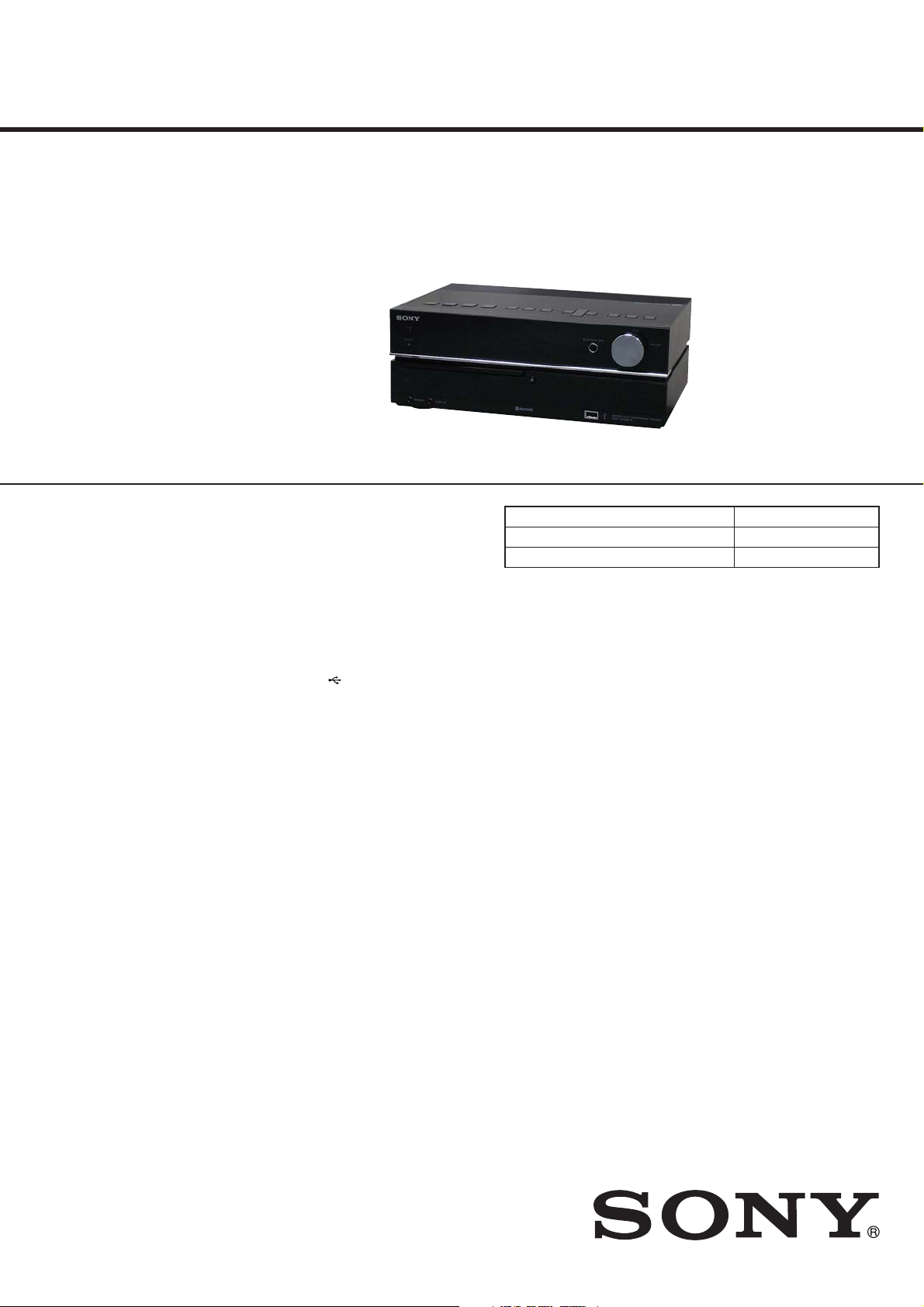
• HCD-HX50BTR is the amplifi er , bluetooth,
USB, CD player and tuner section in CMTHX50BTR.
• HCD-HX70BTR is the amplifi er , bluetooth,
USB, CD player and tuner section in CMTHX70BTR.
• HCD-HX80R is the amplifi er , USB, CD play-
er and tuner section in CMT-HX80R.
• HCD-HX90BTR is the amplifi er , bluetooth,
USB, CD player and tuner section in CMTHX90BTR.
• The Bluetooth word mark and logos are owned by the Bluetooth SIG, Inc. and any use of such
marks by Sony Corporation is under license. Other trademarks and trade names are those of their
respective owners.
• “WALKMAN” and “WALKMAN” logo are registered trademarks of Sony Corporation.
• MPEG Layer-3 audio coding technology and patents licensed from Fraunhofer IIS and Thom-
son.
• Windows Media is a registered trademark of Microsoft Corporation in the United States and/or
other countries.
Amplifier section
HCD-HX80R/HX90BTR
DIN power output (rated):
40 + 40 watts (6 ohms at 1 kHz, DIN)
Continuous RMS power output
(reference): 50 + 50 watts (6 ohms at
1 kHz, 10% THD)
Music power output (reference):
50 + 50 watts (6 ohms at 1 kHz, 10%
THD)
HCD-HX70BTR
DIN power output (rated):
60 + 60 watts (4 ohms at 1 kHz, DIN)
Continuous RMS power output
(reference): 75 + 75 watts (4 ohms at
1 kHz, 10% THD)
Music power output (reference):
75 + 75 watts (4 ohms at 1 kHz, 10%
THD)
HCD-HX50BTR
European and Russian models:
DIN power output (rated):
40 + 40 watts (6 ohms at 1 kHz, DIN)
Continuous RMS power output
(reference): 50 + 50 watts (6 ohms at
1 kHz, 10% THD)
Music power output (reference):
50 + 50 watts (6 ohms at 1 kHz, 10%
THD)
Other models:
DIN power output (rated):
40 + 40 watts (6 ohms at 1 kHz, DIN)
Continuous RMS power output
(reference): 50 + 50 watts (6 ohms at
1 kHz, 10% THD)
Inputs:
AUDIO IN (stereo mini jack):
voltage 250 mV, impedance
22 kilohms
(USB) port: Type A, maximum
current 500 mA
Outputs:
PHONES (stereo mini jack): accepts
headphones of 8 ohms or more
SPEAKER: accepts impedance of
4 ohms (CMT-HX70BTR) or 6 ohms
(CMT-HX50BTR)
Bluetooth section
(HCD-HX50BTR/HX70BTR/HX90BTR)
Communication system:
Bluetooth Standard version 2.0
Output:
Bluetooth Standard Power Class 2
Maximum communication range:
Line of sight approx. 10 m
Frequency band:
2.4 GHz band (2.4000 GHz
– 2.4835 GHz)
Modulation method:
FHSS
Compatible Bluetooth proles
A2DP (Advanced Audio Distribution
Prole)
AVRCP (Audio Video Remote
Control Prole)
Supported codecs:
Receive: SBC (Sub Band Codec), MP3
Transmit: SBC (Sub Band Codec)
2)
Photo: HCD-HX50BTR
SPECIFICATIONS
1)
:
Canadian Model
E Model
HCD-HX50BTR
AEP Model
HCD-HX50BTR/HX70BTR
UK Model
HCD-HX80R/HX90BTR
Model Name Using Similar Mechanism NEW
CD Mechanism Deck BU-K6BD91UR2-WOD
Optical Pick-up Block Name KSM-213DCP
1)
e actual range will vary depending on
factors such as obstacles between devices,
magnetic elds around a microwave oven,
static electricity, reception sensitivity,
antenna’s performance, operating system,
soware application, etc.
2)
Bluetooth standard proles indicate the
purpose of Bluetooth communication
between devices.
USB section
Supported bit rate
MP3 (MPEG 1 Audio Layer-3):
32 – 320 kbps, VBR
WMA: 32 – 192 kbps, VBR
AAC: 48 – 320 kbps
Sampling frequencies
MP3 (MPEG 1 Audio Layer-3):
32/44.1/48 kHz
WMA: 44.1 kHz
AAC: 44.1 kHz
CD player section
System: Compact disc and digital audio
system
Laser Diode Properties
Emission duration: Continuous
Laser Output*: Less than 44.6μW
* is output is the value measurement
at a distance of 200mm from the
objective lens surface on the Optical
Pick-up Block with 7mm aperture.
Frequency response: 20 Hz – 20 kHz
Signal-to-noise ratio: More than 90 dB
Dynamic range: More than 90 dB
Tuner section
DAB tuner section
(HCD-HX80R/HX90BTR) :
Frequency range*
Band-III: 174.928 (5A) – 239.200
(13F) MHz
* For details, see “DAB frequency table”.
Antenna: FM/DAB lead antenna
Antenna terminal: 75 ohms, F female
FM stereo, FM/AM superheterodyne tuner
FM tuner section:
Tuning range
Canadian and Brazilian models:
87.5 – 108.0 MHz (100 kHz step)
Other models: 87.5 – 108.0 MHz
(50 kHz step)
Antenna: FM lead antenna
Antenna terminals: 75 ohms unbalanced
Intermediate frequency: 10.7 MHz
AM tuner section:
Tuning range
European and Russian models:
531 – 1,602 kHz (with 9 kHz tuning
interval)
Canadian and Latin American
models:
530 – 1,710 kHz (with 10 kHz tuning
interval)
531 – 1,710 kHz (with 9 kHz tuning
interval)
Other models:
531 – 1,602 kHz (with 9 kHz tuning
interval)
530 – 1,610 kHz (with 10 kHz tuning
interval)
Antenna: AM loop antenna, external
antenna terminal
Intermediate frequency: 450 kHz
9-889-091-02
2008F05-1
2008.06
©
– Continued on next page –
COMPACT DISC RECEIVER
Sony Corporation
Audio Business Group
Published by Sony Techno Create Corporation
HCD-HX50BTR/HX70BTR/HX80R/HX90BTR
Ver. 1.1
DAB frequency table (Band-III)
Frequency Label Frequency Label
174.928 MHz 5A 209.936 MHz 10A
176.640 MHz 5B 211.648 MHz 10B
178.352 MHz 5C 213.360 MHz 10C
180.064 MHz 5D 215.072 MHz 10D
181.936 MHz 6A 216.928 MHz 11A
183.648 MHz 6B 218.640 MHz 11B
185.360 MHz 6C 220.352 MHz 11C
187.072 MHz 6D 222.064 MHz 11D
188.928 MHz 7A 223.936 MHz 12A
190.640 MHz 7B 225.648 MHz 12B
192.352 MHz 7C 227.360 MHz 12C
194.064 MHz 7D 229.072 MHz 12D
195.936 MHz 8A 230.784 MHz 13A
197.648 MHz 8B 232.496 MHz 13B
199.360 MHz 8C 234.208 MHz 13C
201.072 MHz 8D 235.776 MHz 13D
202.928 MHz 9A 237.488 MHz 13E
204.640 MHz 9B 239.200 MHz 13F
206.352 MHz 9C
208.064 MHz 9D
General
Power requirements
European and Russian models:
220 – 240 V AC, 50/60 Hz
Canadian model: 120 V AC, 60 Hz
Mexican model: 127 V AC, 60 Hz
Argentina model: 220 – 240 V AC,
50/60 Hz
Korean model: 220 – 240 V AC,
50/60 Hz
Latin American models (except for
Mexican and Argentina models):
120 – 127, 220 – 240 V AC, 50/60 Hz,
adjustable with voltage selector
Other models:
220 – 240 V AC, 50/60 Hz
Power consumption
HCD-HX90BRT: 40 watts
HCD-HX80R: 40 watts
HCD-HX70BTR: 50 watts
HCD-HX50BTR: 40 watts
Dimensions (w/h/d) (excl. speakers):
Approx. 305 × 116 × 226 mm
(HCD-HX80R/HX90BTR)
Approx. 305 × 116 × 225 mm
(HCD-HX50BTR/HC70BTR)
Design and specications are subject to
change without notice.
Notes on chip component replacement
• Never reuse a disconnected chip component.
• Notice that the minus side of a tantalum capacitor may be damaged by heat.
Flexible Circuit Board Repairing
• Keep the temperature of soldering iron around 270 °C during
repairing.
• Do not touch the soldering iron on the same conductor of the
circuit board (within 3 times).
• Be careful not to apply force on the conductor when soldering
or unsoldering.
CAUTION
Use of controls or adjustments or performance of procedures other than
those specifi ed herein may result in hazardous radiation exposure.
is appliance is classied as a CLASS 1
LASER product. is marking is located
on the rear exterior.
SAFETY-RELATED COMPONET WARNING!
COMPONENTS IDENTIFIED BY MARK 0 OR DOTTED LINE
WITH MARK 0 ON THE SCHEMATIC DIAGRAMS AND IN
THE PARTS LIST ARE CRITICAL TO SAFE OPERATION.
REPLACE THESE COMPONENTS WITH SONY PARTS
WHOSE PART NUMBERS APPEAR AS SHOWN IN THIS
MANUAL OR IN SUPPLEMENTS PUBLISHED BY SONY.
2
ATTENTION AU COMPOSANT AYANT RAPPORT
À LA SÉCURITÉ!
LES COMPOSANTS IDENTIFIÉS PAR UNE MARQUE 0 SUR
LES DIAGRAMMES SCHÉMATIQUES ET LA LISTE DES
PIÈCES SONT CRITIQUES POUR LA SÉCURITÉ DE FONCTIONNEMENT. NE REMPLACER CES COM- POSANTS QUE
PAR DES PIÈCES SONY DONT LES NUMÉROS SONT DONNÉS DANS CE MANUEL OU DANS LES SUPPLÉMENTS
PUBLIÉS PAR SONY.

HCD-HX50BTR/HX70BTR/HX80R/HX90BTR
TABLE OF CONTENTS
1. SERVICING NOTES ............................................. 4
2. GENERAL .................................................................. 6
3. DISASSEMBLY
3-1. Disassembly Flow ........................................................... 8
3-2. Panel (Top) Block ........................................................... 9
3-3. Panel (Front) Block ......................................................... 9
3-4. Knob Assy ....................................................................... 10
3-5. MAIN Board ................................................................... 10
3-6. Loading Mechanism Block ............................................. 11
3-7. Base Unit (BU-K6BD91UR2-WOD) ............................. 11
3-8. Belt .................................................................................. 12
3-9. Optical Pick-up Block (KSM-213D) .............................. 12
4. TEST MODE ............................................................ 13
5. ELECTRICAL CHECKS ...................................... 15
6. DIAGRAMS
6-1. Block Diagram - CD SERVO Section - .......................... 16
6-2. Block Diagram
- TUNER/USB/BLUETOOTH Section - ........................ 17
6-3. Block Diagram - MAIN Section - ................................... 18
6-4. Block Diagram - AMP Section - ..................................... 19
6-5. Block Diagram - PANEL/POWER SUPPLY - ............... 20
6-6. Printed Wiring Boards - CD Section - ............................ 22
6-7. Schematic Diagram - CD Board - ................................... 23
6-8. Printed Wiring Board - USB Board - .............................. 24
6-9. Schematic Diagram - USB Board - ................................. 25
6-10. Printed Wiring Boards - BLUETOOTH Section
(HX50BTR/HX70BTR/HX90BTR) - ............................. 26
6-11. Schematic Diagram - BLUETOOTH Section
(HX50BTR/HX70BTR/HX90BTR) - ............................. 27
6-12. Printed Wiring Board
- DAB Board (HX80R/HX90BTR) - .............................. 28
6-13. Schematic Diagram
- DAB Board (HX80R/HX90BTR) - .............................. 29
6-14. Printed Wiring Board - MAIN Section - ......................... 30
6-15. Schematic Diagram - MAIN Section (1/3) - ................... 31
6-16. Schematic Diagram - MAIN Section (2/3) - ................... 32
6-17. Schematic Diagram - MAIN Section (3/3) - ................... 33
6-18. Printed Wiring Board
- AMP Board (HX50BTR/HX80R/HX90BTR) - ........... 34
6-19. Schematic Diagram
- AMP Board (HX50BTR/HX80R/HX90BTR) - ........... 35
6-20. Printed Wiring Board - AMP Board (HX70BTR) - ........ 36
6-21. Schematic Diagram - AMP Board (HX70BTR) - ........... 37
6-22. Printed Wiring Boards - INPUT/OUTPUT Section - ..... 38
6-23. Schematic Diagram - INPUT/OUTPUT Section - .......... 39
6-24. Printed Wiring Boards - PANEL Section - ..................... 40
6-25. Schematic Diagram - PANEL Section - .......................... 41
6-26. Printed Wiring Board - SW POWER Board - ................. 42
6-27. Schematic Diagram - SW POWER Board - ................... 43
8. ELECTRICAL PARTS LIST .............................. 64
7. EXPLODED VIEWS
7-1. Panel (Top) Section ......................................................... 57
7-2. Chassis (Top) Section ..................................................... 58
7-3. Panel (Front) Section ...................................................... 59
7-4. Main Section ................................................................... 60
7-5. Chassis Section ............................................................... 61
7-6. Loading Mechanism Section .......................................... 62
7-7. Base Unit Section (BU-K6BD91UR2-WOD) ................ 63
3
HCD-HX50BTR/HX70BTR/HX80R/HX90BTR
Ver. 1.1
SECTION 1
SERVICING NOTES
NOTES ON HANDLING THE OPTICAL PICK-UP
BLOCK OR BASE UNIT
The laser diode in the optical pick-up block may suffer electrostatic break-down because of the potential difference generated by the
charged electrostatic load, etc. on clothing and the human body.
During repair, pay attention to electrostatic break-down and also
use the procedure in the printed matter which is included in the
repair parts.
The fl exible board is easily damaged and should be handled with
care.
NOTES ON LASER DIODE EMISSION CHECK
The laser beam on this model is concentrated so as to be focused
on the disc refl ective surface by the objective lens in the optical
pickup block. Therefore, when checking the laser diode emission,
observe from more than 30 cm away from the objective lens.
UNLEADED SOLDER
Boards requiring use of unleaded solder are printed with the leadfree mark (LF) indicating the solder contains no lead.
(Caution: Some printed circuit boards may not come printed with
the lead free mark due to their particular size)
: LEAD FREE MARK
Unleaded solder has the following characteristics.
• Unleaded solder melts at a temperature about 40 °C higher
than ordinary solder.
Ordinary soldering irons can be used but the iron tip has to be
applied to the solder joint for a slightly longer time.
Soldering irons using a temperature regulator should be set to
about 350 °C.
Caution: The printed pattern (copper foil) may peel away if the
heated tip is applied for too long, so be careful!
• Strong viscosity
Unleaded solder is more viscous (sticky, less prone to fl ow)
than ordinary solder so use caution not to let solder bridges
occur such as on IC pins, etc.
• Usable with ordinary solder
It is best to use only unleaded solder but unleaded solder may
also be added to ordinary solder.
MODEL IDENTIFICATION
– Back Panel –
Model Part No.
HX50BTR: AEP model
HX50BTR: Canadian model
HX50BTR: Russian model
HX50BTR: Singapore model
HX50BTR: Korean model
HX50BTR: Mexican model
HX50BTR: Chilean and Peruvian models
HX50BTR: Argentina model
HX50BTR: Brazilian model
HX70BTR
HX90BTR
HX80R
PART No.
3-284-497-0[]
3-284-497-1[]
3-284-497-2[]
3-284-497-3[]
3-284-497-5[]
3-284-497-7[]
3-284-497-8[]
3-284-497-9[]
3-290-773-0[]
3-290-773-1[]
3-290-773-2[]
3-290-773-3[]
RELEASING THE ANTITHEFT LOCK
The disc tray lock function for the antitheft of an demonstration
disc in the store is equipped.
Releasing Procedure:
1. Press the [
2. While pressing the [
] button to turn the power on.
?/1
x/CANCEL
] button, press the [
Z
] button unit “UNLOCKED” displayed on the fl uorescent indicator
tube (around 5 seconds) .
Note: When “LOCKED” is displayed, the tray lock is not released by
turning power on/off with the [?/1] button.
NOTE THE IC904 ON THE BT BOARD REPLACING
When IC904 cannot exchange with single. When IC904 is damaged, exchange the entire mounted board.
4

HCD-HX50BTR/HX70BTR/HX80R/HX90BTR
HOW TO OPEN THE TRAY WHEN POWER SWITCH TURN OFF
Remove the panel (side R).
(Illustration of disaaaembly is omitted.)
Make a small hole in the location
of the figure.
12 mm
12 mm
Open the tray.
chassis (main)
– chassis (main) side R view –
panel (front) block
Insert the driver.
ATTENTION WHEN INSTALLING Q12
Note 1: Be sure to use an original screw
(Part. No. 7-685-646-79 SCREW +BVTP 3X8 TYPE2 IT-3),
never use a screw longer than an original screw.
panel (back)
Q12
heatsink (REG)
screw (BVTP3x8)
Push the lever.
SW POWER board
chassis (main)
SW POWER board
chassis (main)
Q12
more than 5 mm
Note 2: Open more than 5 mm of screw (BVTP3x8)
installing Q12 in heatsink (REG)
to a chassis (main) from a screw point.
5
HCD-HX50BTR/HX70BTR/HX80R/HX90BTR
SECTION 2
GENERAL
This section is extracted
from instruction manual.
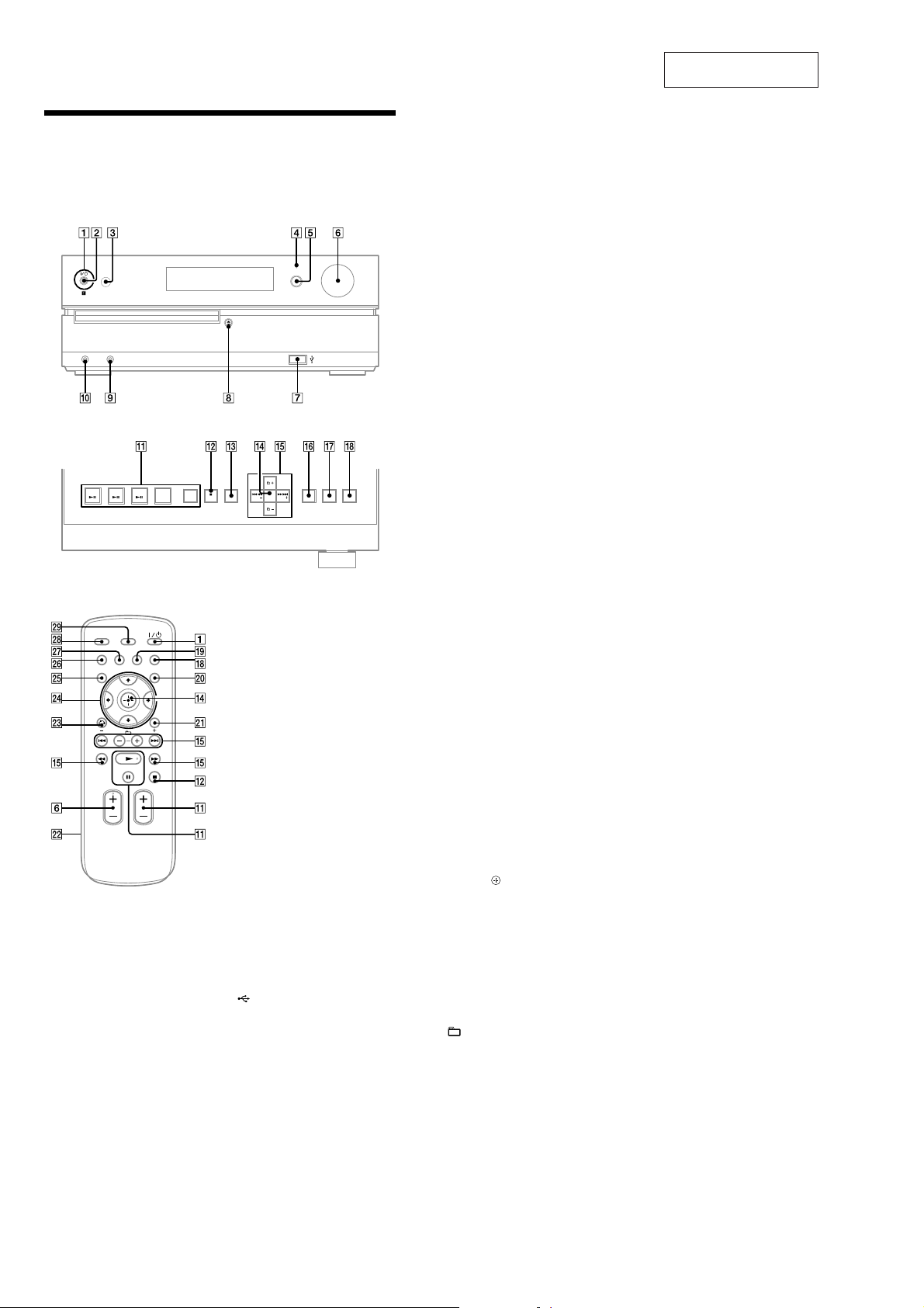
Guide to parts and controls
is manual mainly explains operations using the remote, but the same operations can
also be performed using the buttons on the unit having the same or similar names.
Unit
Front panel
Top panel
Remote (RM-AMU009)
/ (power) button
Press to turn on the system.
STANDBY indicator
Lights up when the system is turned o.
Remote sensor
BLUETOOTH indicator (HX50BTR/
HX70BTR/HX90BTR only)
Lights up when the Bluetooth function
is active.
BLUETOOTH button (HX50BTR/
HX70BTR/HX90BTR only)
Press to make a connection,
disconnection, or pairing with a
Bluetooth device.
Unit: VOLUME control
Remote: VOLUME +/– button
Turn or press to adjust the volume.
(USB) port
Connect to an optional USB device.
(open/close) button
Press to open or close the disc tray.
AUDIO IN jack
Connect to an optional audio
component.
PHONES jack
Connect the headphones.
Playback buttons and function
buttons
Unit: BLUETOOTH (play/
pause) button (HX50BTR/
HX70BTR/HX90BTR only)
Press to select the Bluetooth function.
Press to start or pause playback of the
music on the Bluetooth device (Bluetooth
mobile phone, etc.).
Unit: USB (play/pause)
button
Press to select the USB function.
Press to start or pause playback of an
optional USB device.
Unit: CD (play/pause)
button
Press to select the CD function.
Press to start or pause playback of a disc.
Remote: (play) button,
(pause) button
Press to start or pause playback.
Unit: TUNER/BAND button
Press to select the TUNER function.
Press to select FM or AM reception
mode.
Unit: DMPORT (play/pause)
button (HX80R only)
Press to select the DMPORT function.
Press to start or pause playback of the
audio device connected to the DIGITAL
MEDIA PORT adapter.
Unit: FUNCTION button
Remote: FUNCTION +/– button
Press to select the function.
Unit: /CANCEL (stop/cancel)
button
Remote: (stop) button
Press to stop playback.
Press to cancel search.
SEARCH button (HX50BTR/
HX70BTR)
Press to enter or exit search mode.
SEARCH/DAB AUTO SCAN button
(HX80R/HX90BTR)
Press to enter or exit search mode.
Press to run the DAB Automatic Scan.
Unit: ENTER button
Remote:
Press to enter the settings.
(enter) button
/ (go back/go forward)
button
Press to select a track or le.
Unit: TUNE +/– (tuning) button
Remote: +/– (tuning) button
Press to tune in the desired station.
+/– (select folder) button
Press to select a folder.
/ (rewind/fast forward)
button
Press to nd a point in a track or le.
CD-USB SYNC/REC1 button
Press to record from a disc onto the
connected optional USB device.
USB MENU button
Press to erase audio les and folders from
the connected optional USB device.
Press to select which memory to read
to if the USB device has more than one
memory.
Sound buttons
Unit: DSGX button
Remote: EQ button
Press to select the sound eect.
CLEAR button
Press to delete a pre-programmed track
or le.
Press to erase the pairing registration
information of the Bluetooth device.
TIMER MENU button
Press to set the clock and the Play Timer.
TOOL MENU button
Press to select a menu when using the
DIGITAL MEDIA PORT adapter.
Battery compartment lid
RETURN button
Press to return to the previous menu
when using the DIGITAL MEDIA PORT
adapter.
/// button
Press to select the menu items.
TUNER MEMORY button
Press to preset the radio station.
PLAY MODE/TUNING MODE
button
Press to select the play mode of a CD,
MP3 disc or an optional USB device.
Press to select the tuning mode.
XK
REPEAT/FM MODE button
Press to listen to a disc, a single track or
le repeatedly.
Press to select the FM reception mode
(monaural or stereo).
XL
SLEEP button
Press to set the Sleep Timer.
XM
DISPLAY button
Press to change the information on the
display.
6
HCD-HX50BTR/HX70BTR/HX80R/HX90BTR
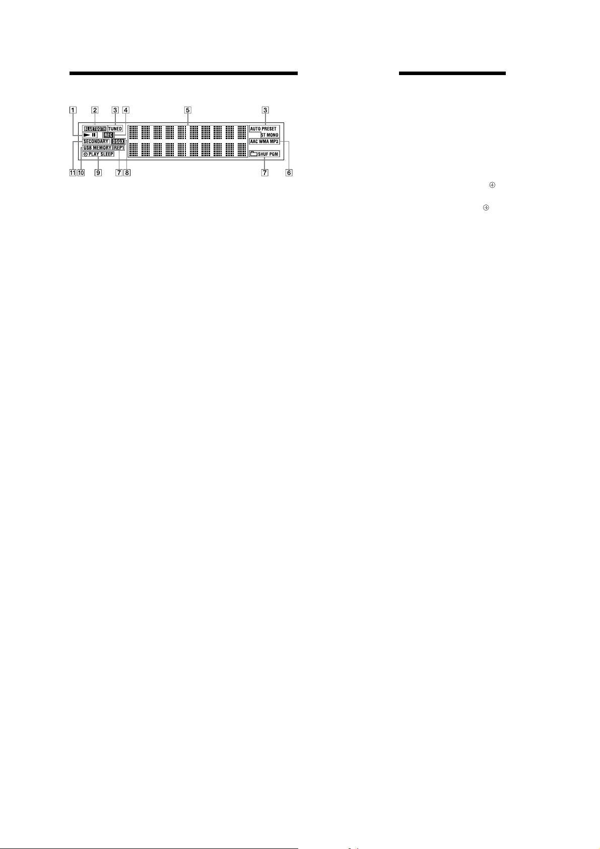
Information on the display
Play/Pause
BLUETOOTH (HX50BTR/HX70BTR/
HX90BTR only)
Lights up when the Bluetooth function
is selected.
Tuner reception mode
Tuner reception
REC
Text information
Audio format
Play mode
DSGX
Timer
USB MEMORY
Lights up when an optional USB device
is connected.
DAB service reception (HX80R/
HX90BTR only)
Lights up when secondary service is
received.
Setting the clock
Use buttons on the remote to set the
clock.
1
Press / to turn on the
system.
2
Press TIMER MENU .
e hour indication ashes in the
display.
If “PLAY SET?” ashes in the display,
press / repeatedly to select
“CLOCK SET?” and then press .
3
Press / repeatedly to set
the hour, and then press
4
Use the same procedure to set
the minutes.
e clock settings are lost when you
disconnect the power cord or if a
power failure occurs.
To display the clock when the system
is off
Press DISPLAY XM. e clock is displayed
for about 8 seconds.
.
7
HCD-HX50BTR/HX70BTR/HX80R/HX90BTR
SECTION 3
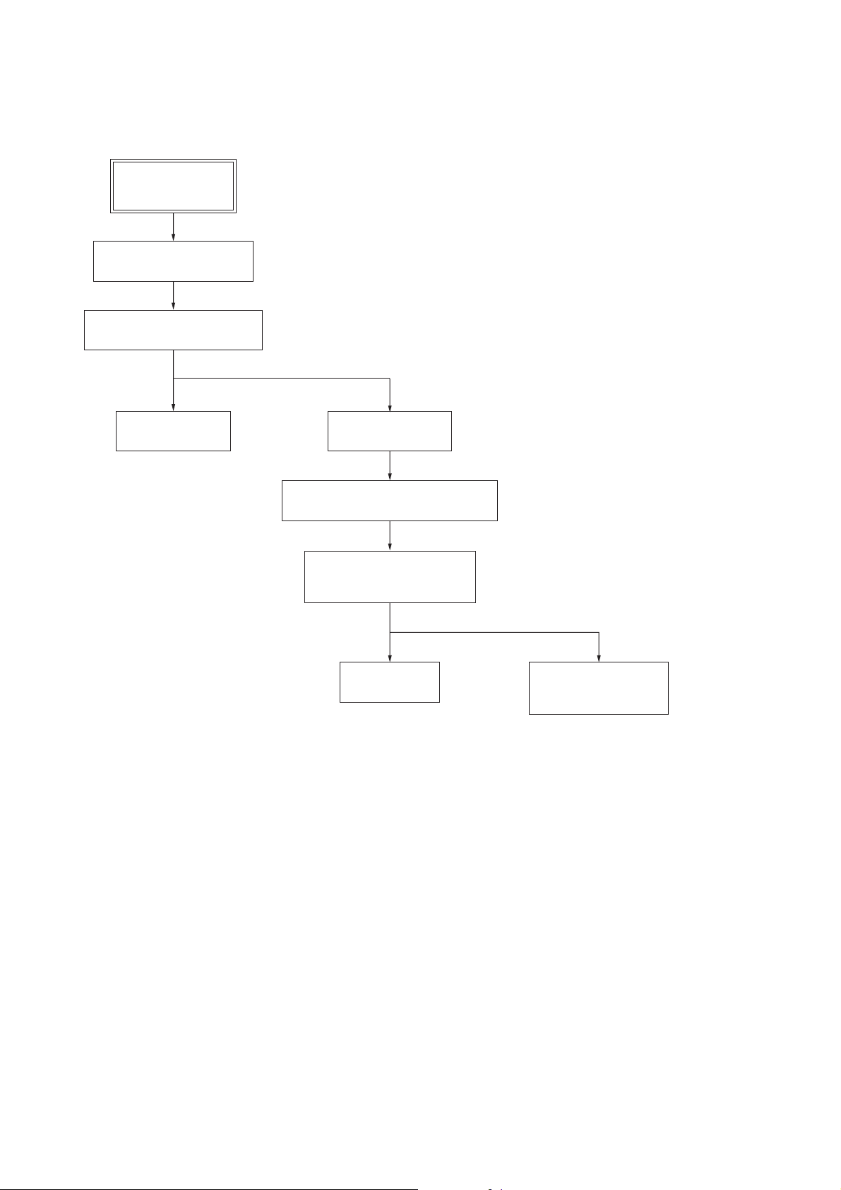
DISASSEMBLY
• This set can be disassembled in the order shown below.
3-1. DISASSEMBLY FLOW
SET
3-2. PANEL (TOP) BLOCK
(Page 9)
3-3. PANEL (FRONT) BLOCK
(Page 9)
3-4. KNOB ASSY
(Page 10)
3-5. MAIN BOARD
(Page 10)
3-6. LOADING MECHANISM BLOCK
(Page 11)
3-7. BASE UNIT
(BU-K6BD91UR2-WOD)
(Page 11)
3-8. BELT
(Page 12)
3-9. OP BASE ASSY
(KSM-213D)
(Page 12)
8
Note: Follow the disassembly procedure in the numerical order given.
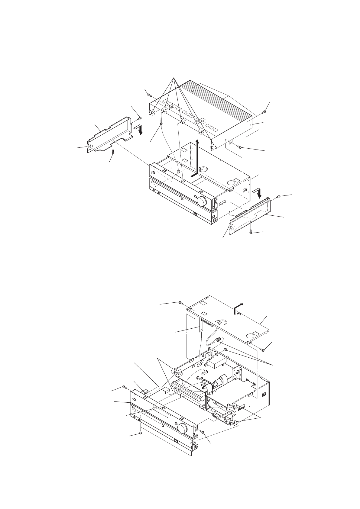
3-2. PANEL (TOP) BLOCK
five claws
RG
screw
RT
(BVTP3 × 8)
screw
(BVTP3 × 8)
panel (side L)
R
connector
claw
screw
(BVTP3 × 8)
RI
(CN507)
HCD-HX50BTR/HX70BTR/HX80R/HX90BTR
three screws
RE
(BVTP3 × 8)
panel (top) block
RK
screw
RB
RH
(BVTP3 × 8)
screw
(BVTP3 × 8)
3-3. PANEL (FRONT) BLOCK
flexible flat cable (11 core)
(CN518)
(HX80R/HX90BTR)
flexible flat cable (15 core)
(CN502)
connector
R
(CN501)
screw
(BVTP3 × 8)
panel (front) block
RE
screw
(BVTP3 × 8)
two claws
RT
claw
panel (side R)
screw
(BVTP3 × 8)
chassis (top) block
screw
(BVTP3 × 8)
DAB cable
(HX80R/HX90BTR)
flexible flat cable (15 core)
(CN609)
two screws
(BVTP3 × 8)
screw
(BVTP3 × 8)
two claws
RB
9
HCD-HX50BTR/HX70BTR/HX80R/HX90BTR
Ver. 1.1
3-4. KNOB ASSY
Insert a screw driver into the position shown in the fig
and push it to remove the knob assy,
not giving an excessive force.
knob assy
panel (front) block
knob assy
hole
screw driver
PANEL board back view
3-5. MAIN BOARD
flexible flat cable (11 core)
(CN502)
screw
RT
(BVTP3 × 8)
earth wire
RE
(HX80R/HX90BTR)
flexible flat cable (19 core)
(CN510)
MAIN board
RG
connector
(CN504)
three screws
RB
(BVTP3 × 8)
flexible flat cable (9 core)
(HX50BTR: CND, RU, E51, MX, BR, SP, AR, KR models),
flexible flat cable (11 core)
(HX50BTR: AEP/HX70BTR/HX80R/HX90BTR)
(tuner (FM/AM), MAIN board (CN518))
tuner (FM/AM)
connector
R
(CN908)
two screws
(BVTP3 × 8)
flexible flat cable (27 core)
(CN701)
flexible flat cable (21 core)
(CN751)
10
flexible flat cable (5 core)
(CN720)
• Abbreviation
AR : Argentina model
BR : Brazilian model
CND : Canadian model
E51 : Chilean and Peruvian model
KR : Korean model
MX : Mexican model
RU : Russian model
SP : Singapore model
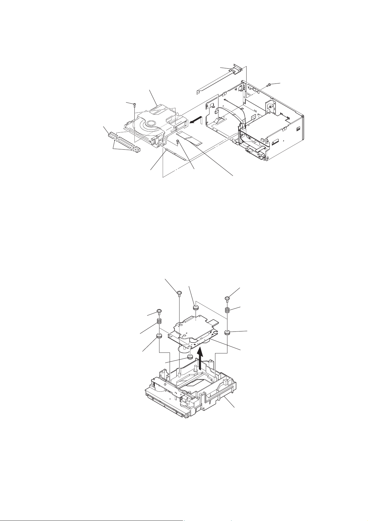
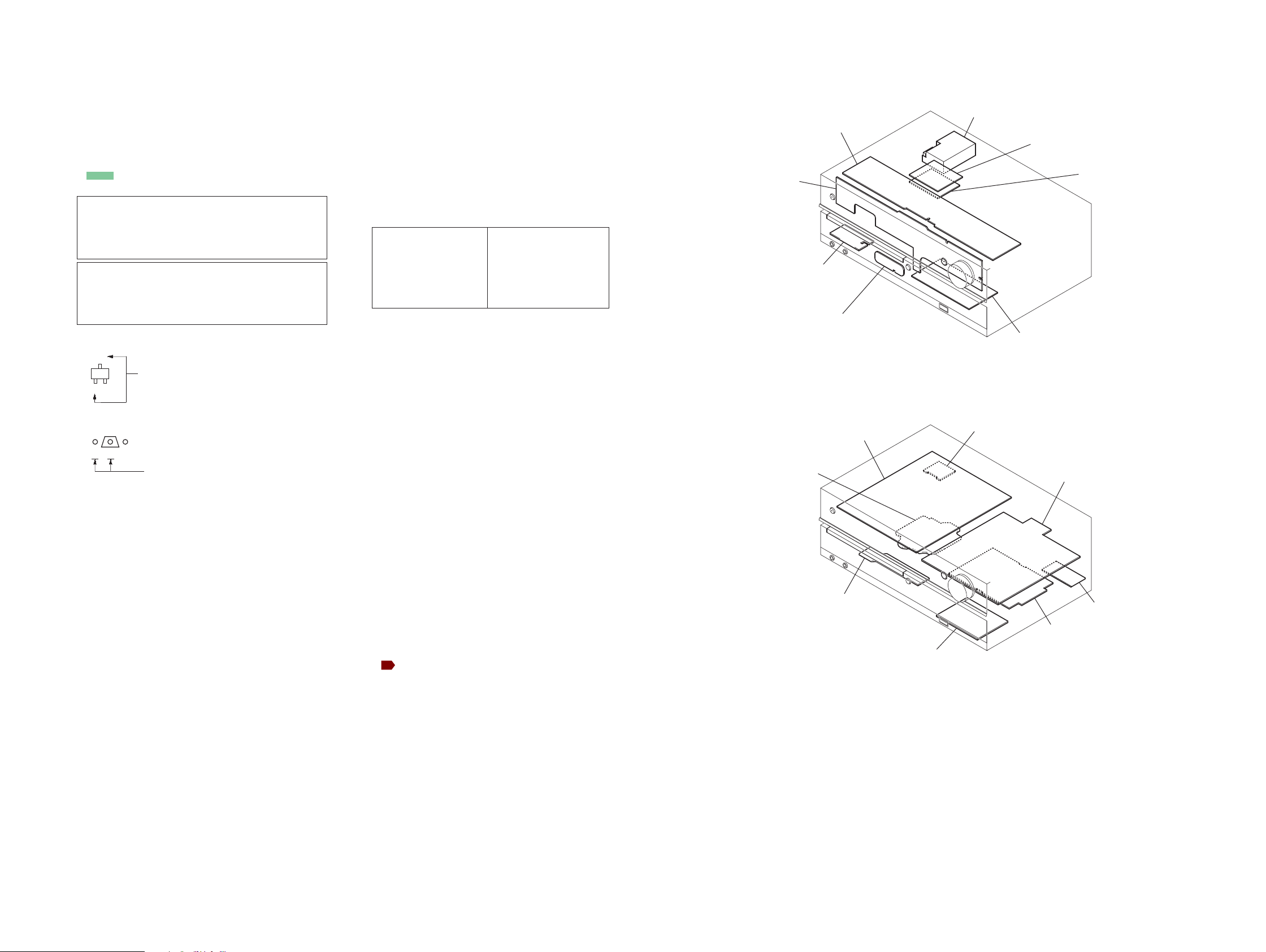
3-6. LOADING MECHANISM BLOCK
loading mechanism block
R
two screws
(BV3)
panel (CD)
two claws
flexible flat cable (5 core)
(CN001)
HCD-HX50BTR/HX70BTR/HX80R/HX90BTR
DMP board block
screw
(BVTP3 × 8)
screw
(BV3)
flexible flat cable (27 core)
(CN202)
3-7. BASE UNIT (BU-K6BD91UR2-WOD)
floating screw
two floating screws
two springs (insulator)
insulator
insulator
insulator
– Bottom view –
two floating screws
two springs
(insulator)
insulator
base unit
(BU-K6BD91UR2-WOD)
loading (BK) assy
11
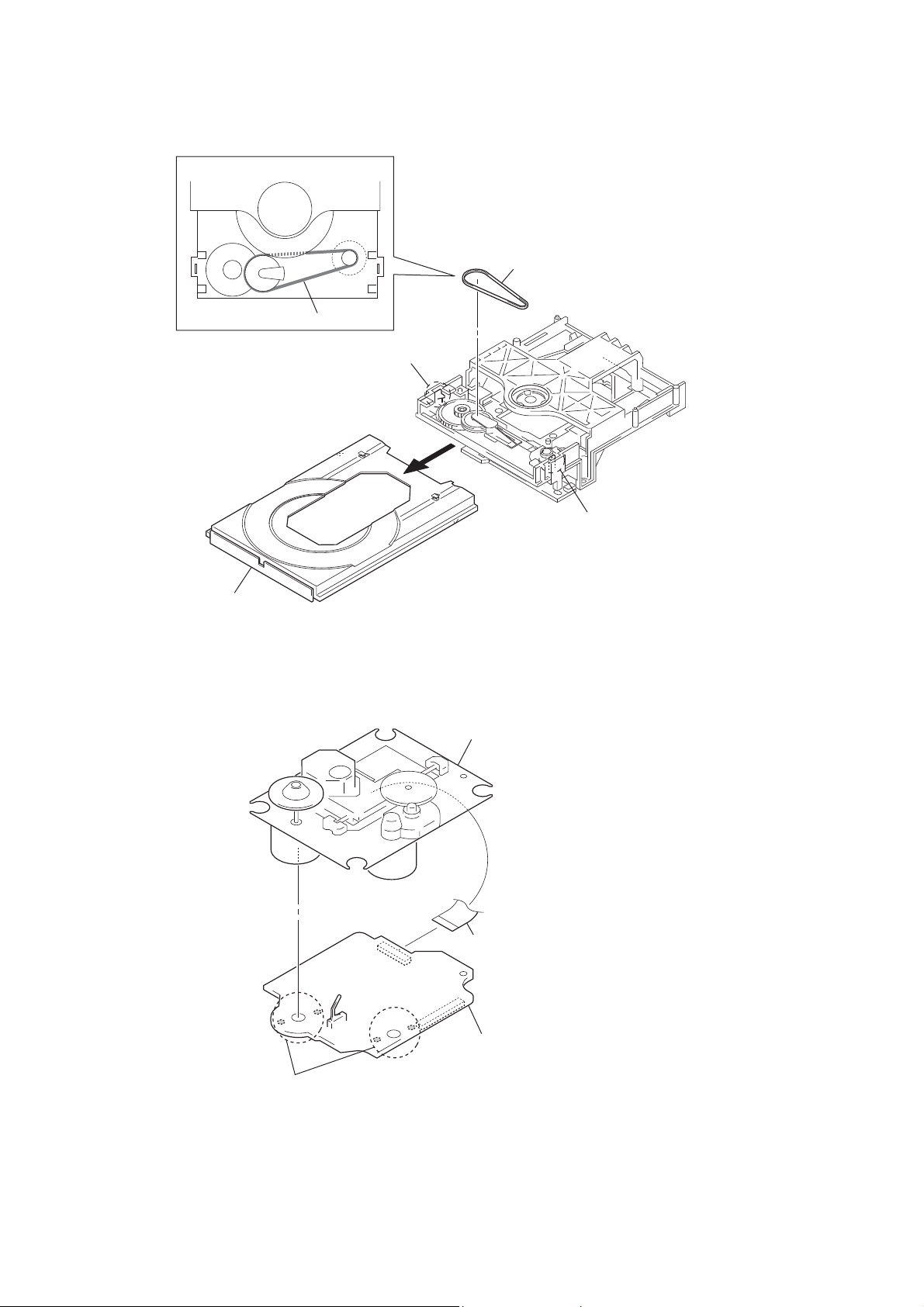
HCD-HX50BTR/HX70BTR/HX80R/HX90BTR
3-8. BELT
position of belt
belt
claw
belt
tray (AU)
3-9. OPTICAL PICK-UP BLOCK (KSM-213D)
claw
op base assy
(KSM-213D)
flexible flat cable (16 core)
(CN301)
12
CD board
Remove four solders.

HCD-HX50BTR/HX70BTR/HX80R/HX90BTR
SECTION 4
TEST MODE
Ver. 1.1
COLD RESET
The cold reset clears all data including preset data stored in the
RAM to initial conditions. Execute this mode when returning the
set to the customer.
Procedure:
1. Press three buttons of [x/CANCEL], [DSGX] and [?/1] simultaneously.
2. The system is reset and becomes standby states.
COMMON TEST MODE
This mode is used to check operations of amplifi er.
Procedure:
1. Press the [
2. Press three buttons of [x/CANCEL], [ENTER] and [Z] simultaneously.
3. When the COMMON test mode is activated, “AUDIO IN”
is displayed on the fl uorescent indicator tube and “c PLAY
SLEEP” blink on the fl uorescent indicator tube.
4. Each time [EQ] button on the remote commander is pressed,
the display changes starting “TONE MAX”, “TONE MIN”
and “TONE FLAT” this order.
5. Turn the [VOLUME] knob counterclockwise, “VOLUME
MIN” is displayed on the fl uorescent indicator tube. Turn the
[VOLUME] knob clockwise, “VOLUME MAX” is displayed
on the fl uorescent indicator tube.
6. To release this mode, press the [
PANEL TEST MODE
This mode is used to check the fl uorescent indicator tube, LED,
model, destination, software version and key.
Procedure:
1. Press the [?/1] button to turn the power on.
2. Press three buttons of [x/CANCEL], [DSGX] and [Z] simultaneously.
3. All segments on the fl uorescent indicator tube, [STANDBY]
LED and [BLUETOOTH OPR] LED (HX50BTR/HX70BTR/
HX90BTR only) light up.
4. Press the [DSGX] button, the model and destination are displayed on the fl uorescent indicator tube.
5. Press the [DSGX] button again, MC version is displayed on
the fl uorescent indicator tube.
6. Each time [DSGX] button is pressed, the display changes
starting from MC version, GC version, USBL version , USBM
version, BT version (HX50BTR/HX70BTR/HX90BTR only),
CLA version, CD version, CDD version, CDMA version,
CDMB version, BDA version, BDB version, ST version, TA
version and TM version this order, and returns to the MC version display.
7. When [SEARCH] button is pressed while the MC version is
displayed, year, month and day of the software creation is displayed. When [SEARCH] button is pressed again, the display
returns to the MC version display.
8. Press the [ENTER] button, the key test mode is activated and
“K 0 V0” is displayed on the fl uorescent indicator tube.
9. Each time a button is pressed, “K” value increases. However,
once a button is pressed, it is no longer taken into account.
All keys are pressed, display becomes “K17” (HX80R) or
“K18” (HX50BTR/HX70BTR/HX90BTR).
10. “V” value increases 2, 4, 6 ... if turn the [VOLUME] knob
clockwise, or it decreases 8, 6, 4 ... if turn the knob counterclockwise
11. To release this mode, press three buttons in the same manner as
step 2, or disconnect the power cord.
] button to turn the power on.
?/1
?/1
] button.
TUNER STEP CHANGE
(HX50BTR: Canadian, Chilean, Peruvian, Mexican, Brazilian, Singapore, Argentina and Korean models)
A step of AM tuning interval can be changed over between 9 kHz
or 10 kHz.
Procedure:
1. Press the [?/1] button to turn the power on.
2. Press the [TUNER/BAND] button to select “AM”.
3. Press the [
4. Press two buttons of [TUNER/BAND] and [
ously.
5. The message “AM 9kHz Step” or “AM 10kHz Step” is displayed on the fl uorescent indicator tube and thus the tuning
interval is changed over.
CD SHIP MODE
This mode moves the optical pick-up to the position durable to
vibration. Use this mode when returning the set to the customer
after repair.
Procedure:
1. Press the [?/1] button to turn the power on.
2. Press the [FUNCTION] button to select “CD”.
3. Press two buttons of [SEARCH] and [
4. After the “STANDBY” display blinks, “LOCK” is displayed
on the fl uorescent indicator tube, the ship mode is set.
CD SHIP MODE & MEMORY CLEAR
This mode is used to perform CD ship mode and cold reset simultaneously.
Procedure:
1. Press the [
2. Press three buttons of [SEARCH], [DSGX] and [?/1] simultaneously.
3. After the “STANDBY” display blinks, “LOCK” is displayed
on the fl uorescent indicator tube the ship mode is set and the
system is reset.
ANTITHEFT LOCK MODE
This mode is used to unable to take sample disc out of disc tray in
the shop.
Procedure:
1. Press the [?/1] button to turn the power on.
2. Press the [Z] button to open the disc tray and set the CD disc.
3. Press the [Z] button to close the disc tray.
4. Press two buttons of [x/CANCEL] and [Z] for 5 seconds.
5. The message “LOCKED” is displayed on the fl uorescent indi-
cator tube and the disc tray is locked. (Even if pressing the [Z]
button, the message “LOCKED” is displayed on the fl uores-
cent indicator tube and the disc tray is locked)
6. To release from this mode, press two buttons of [x/CANCEL]
and [Z] for 5 seconds.
7. The message “UNLOCKED” is displayed on the fl uorescent
indicator tube and the disc tray is unlocked.
CD POWER MANAGE
This mode is used to changed over CD power on/off for decreasing
of reception noise in the tuner mode.
Procedure:
1. Press the [?/1] button to turn the power on.
2. Press the [FUNCTION] button to select “CD”.
3. Press the [
4. Press two buttons of [
5. The message “CD POWER ON” or “CD POWER OFF” is displayed on the fl uorescent indicator tube, and CD power on/off
is changed over in the tuner mode.
] button again to turn the power off.
?/1
?/1
] button to turn the power on.
?/1
] button again to turn the power off.
?/1
/CANCEL] and [?/1] simultaneously.
x
] simultane-
?/1
] simultaneously.
13

HCD-HX50BTR/HX70BTR/HX80R/HX90BTR
CD SERVICE MODE
This mode can run the CD sled motor freely. Use this mode, for
instance, when cleaning the optical pick-up.
Procedure:
1. Press the [?/1] button to turn the power on.
2. Press the [FUNCTION] button to select “CD”.
3. Press three buttons of [SEARCH], [ +] and [Z] simultaneously, the message “SERVICE MODE” is displayed on the
fl uorescent indicator tube.
4. Press the [ –] button to move the optical pick-up to inside
track and the message “SLED IN” is displayed on the fl uores-
cent indicator tube, or press the [ +] button to outside track
and the message “SLED OUT” is displayed on the fl uorescent
indicator tube.
5. Press the [DSGX] button, “LD ON” or “LD OFF” is displayed
on the fl uorescent indicator tube. Each time [DSGX] button is
pressed, laser diode on/off is changed over.
6. To release this mode, press the [
BT TEST MODE
(XH50BTR/HX70BTR/HX90BTR)
This mode is used to check the fi rmware version and address of
bluetooth module.
Procedure:
1. Press the [
2. Press the [FUNCTION] button to select “BLUETOOTH”.
3. Press three buttons of [SEARCH], [FUNCTION] and [BLUTOOTH OPR] simultaneously, the message “BT Test” is displayed on the fl uorescent indicator tube. Then, the display is
automatically changed to the fi rmware version of bluetooth
module.
4. Press the [DISPLAY] button on the remote commaner, address
of bluetooth module is displayed on the fl uorescent indicator
tube.
5. To release this mode, press the [?/1] button.
] button to turn the power on.
?/1
?/1
] button.
14

HCD-HX50BTR/HX70BTR/HX80R/HX90BTR
HCD-HX50BTR/HX70BTR/HX80R/HX90BTR
1515
SECTION 5
ELECTRICAL CHECKS
FM TUNE LEVEL CHECK
Procedure:
1. Turn on the set.
2. Input the following signal from signal generator to FM antenna
input directly.
Carrier frequency : A = 87.5 MHz, B = 98 MHz, C = 108 MHz
Deviation :75 kHz
Modulation : 1 kHz
ANT input : 35 dBu (EMF)
Note: Use 75 ohm coaxial cable to connect signal generator and the set.
You cannot use video cable for checking.
Use signal generator whose output impedance is 75 ohm.
3. Set to FM tuner function and tune A, B and C signals.
4. Confi rm “TUNED” is lit on the display for A, B and C sig-
nals.
When the selected station signal is received in good condition,
“TUNED” is displayed.
Note:
1. CD Block is basically constructed to operate without adjustment.
2. Use YEDS-18 disc (3-702-101-01) unless otherwise indicated.
3. Use an oscilloscope with more than 10 MΩ impedance.
4. Clean the object lens by an applicator with neutral detergent
when the signal level is low than specifi ed value with the fol-
lowing checks.
5. Check the focus bias check when optical pick-up block is replaced.
FOCUS BIAS CHECK
Procedure:
1. Connect oscilloscope to TP121 (RFI) and TP124 (VC) on the
CD board.
2. Press the [?/1] button to turn the power on.
3. Set disc (YEDS-18) on the disc tray and press the [CD u]
button to playback.
4. Confi rm that oscilloscope waveform is as shown in the fi gure
below. (eye pattern)
A good eye pattern means that the diamond shape (◊) in the
center of the waveform can be clearly distinguished.
VOLT/DIV: 200 mV
TIME/DIV: 500 ns
level:
1.2 ± 0.3 Vp-p
Checking Location:
TUNER SECTION CD SECTION
signal
generator
set
oscilloscope
(DC range)
CD board
TP121 (RFI)
TP124 (VC)
+
–
– CD Board (Conductor Side) –
TP124
(VC)
TP121
(RFI)
IC101
HCD-HX50BTR/HX70BTR/HX80R/HX90BTR
HCD-HX50BTR/HX70BTR/HX80R/HX90BTR
1616
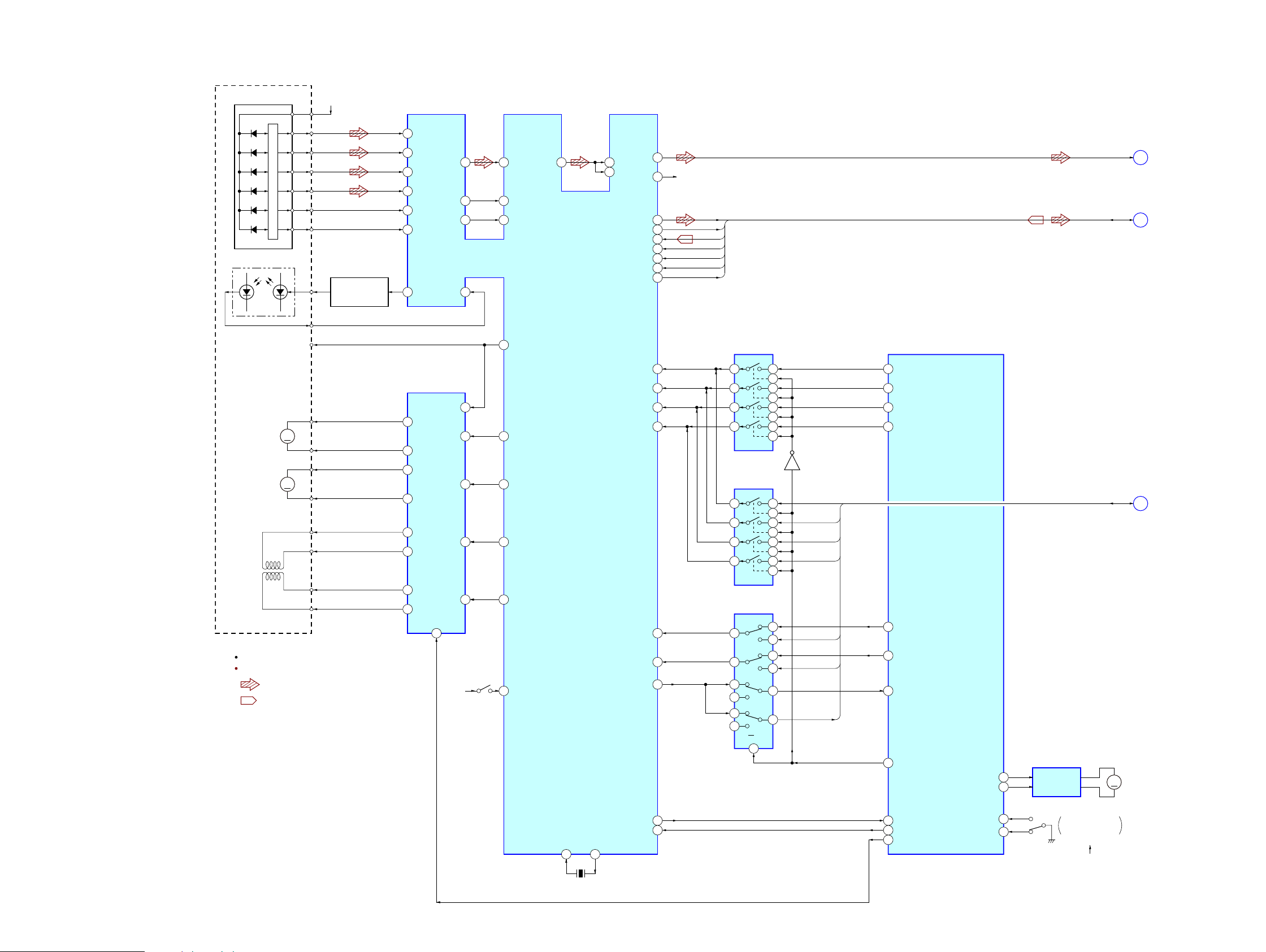
SECTION 6
DIAGRAMS
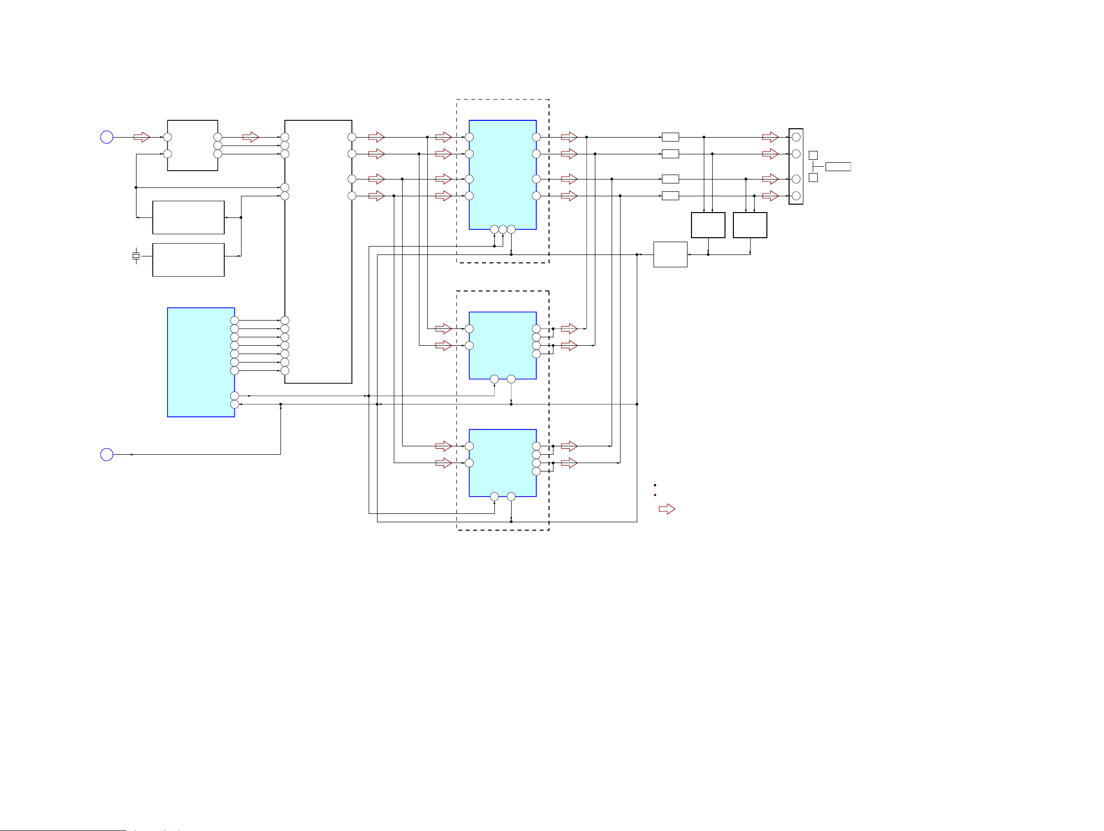
6-1. BLOCK DIAGRAM - CD SERVO Section -
SYSTEM CONTROLLER
IC301 (1/5)
CD-MP3 PROCESSOR
IC101
MUTE
2-AXIS
DEVICE
(TRACKING)(FOCUS)
95
89
A
AVDD
+3.3V
DETECTOR
FNi1 (A)
RFo
97 FPi1 (B)
88
2
AGCi
3RFRP RFZi
76TEi TEZi
83RFEQo 81 RFi
82 RFRPi
30LO
27RO
65AIN (PI4)
66BCKi (PI5)
BCK
A-IN
BUS1
BUS0
BUS2
BUS3
BUCK
67LRCKi (PI6)
LRCK
51PIO3
GATE
49PIO1
ST-REQ
38BUS0
R-CH
94 FNi2 (C)
96 FPi2 (D)
100 TNi (E)
98 TPi (F)
91 LDo 92MDi
2VO1+
1VO1–
13 DMO
AUTOMATIC
POWER CONTROL
Q301
LD
PD
LASER DIODE
OPTICAL PICK-UP
BLOCK
(KSM-213DCP)
B
C
D
E
F
12 FMO
10 TRo
9FOo
20 IO0 (/HSO)
I-V AMP
M401
(SPINDLE)
M402
(SLED)
12 VO2–
11 VO2+
18 VO3+
17 VO3–
26 VO4+
27
7
IN4’
24
IN3’ 20
IN2’
9
IN1
3
BIAS
23
84 VRo
VO4–
M
M
FOCUS/TRACKING COIL DRIVE,
SLED/SPINDLE MOTOR DRIVE
IC401
S201
(LIMIT)
DVDD
+3.3V
24
XO
23
XI
X102
16.9344MHz
95 CD DRIVER MUTE
LOADING
MOTOR DRIVE
IC701
CDM LOAD IN
53
CDM LOAD OUT
CDM OPEN SW
CDM CLOSE SW
54
51
52
M
A
CD-L
B
DATA, CLOCK,
A-IN, BCK, LRCK,
GATE, ST-REQ
C
BUS0 – BUS3,
BUCK, CCE, REQ
: CD PLAY
SIGNAL PATH
R-ch is omitted due to same as L-ch.
: USB
VCC
A
B
C
D
E
F
LD
PD
SP+
VC
SP–
SL+
SL–
T+
T–
F+
F–
1 2 3 CD BUS0
13
39BUS1 4 3 2 CD BUS1
5
40BUS2 (SO) 8 9 1 CD BUS2
23 CD CLK
6
41BUS3 (SI) 11 10 100 CD BUS3
12
BUS SWITCH
IC754
1 2
13
4 3
5
8 9
6
11 10
12
BUS SWITCH
IC753
DATA SELECTOR
IC751
A/B
Q352
42BUCK (CLK) 4
2
3
CCE
21 CD CCE
43XCCE
54SBSY
48PIO0
7
7 MP3 IREQ
25 DEC BUS SEL
19 SBSY
37XRST 94 CD XRST
5
REQ
6
12
14
13
9
10
11
1
S001
DISC TRAY
OPEN/CLOSE DETECT
OPEN
CLOSE
M001
(LOADING)
47AOUT2 (PO5)
63BCK (PO8)
CLOCK
DATA
(Page 18)
(Page 17)
(Page 17)
HCD-HX50BTR/HX70BTR/HX80R/HX90BTR
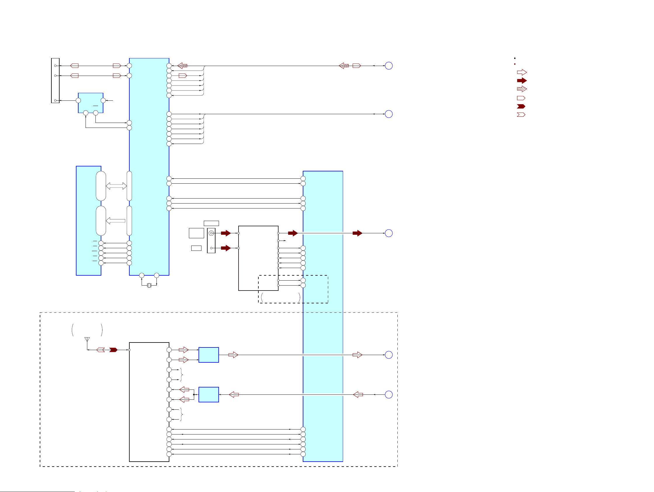
HCD-HX50BTR/HX70BTR/HX80R/HX90BTR
1717
6-2. BLOCK DIAGRAM - TUNER/USB/BLUETOOTH Section -
BUS1
BUS0
BUS2
BUS3
BUCK
CCE
REQ
LB
I/O0 – I/O15
D0 – D15
S-RAM
IC921
39
UB
40
OE
41
WE
17
CE
6
79 D+
80 D–
77 USBOC
USB CONTROLLER
IC901
35 USB TXD_OUT
SYSTEM CONTROLLER
IC301 (2/5)
CN902
(USB)
3
2
1
D+
D–
78 USBPON
70 CS2
64
RD
65 WR
66 SRLLB
67 SRLUB
VBUS
B
DATA, CLOCK,
A-IN, BCK, LRCK,
GATE, ST-REQ
C
BUS0 – BUS3,
BUCK, CCE, REQ
VBUS POWER
ON/OFF SWITCH
IC915
5
1
4OUT
EN
3
FLG
IN
VBUS
+5V
93DATA
92BCK
BCK
A-IN
LRCK
GATE
ST-REQ
71LRCK
94GATE
97ST-REQ
55BUS0
56BUS1
88RXD1
36 USB RXD_IN87TXD1
38 USB RTS2DI
6 USB_CTS84DO
5 USB_RESET1/RESET
57BUS2
58BUS3
59/BUCK
60/CCE
96REQ
7 – 10, 13 – 16,
29 – 32, 35 – 38
18 – 25, 28 – 35
A0 – A15
A1 – A16
44 – 42, 27 – 24,
21 – 18, 5 – 1
37 – 43, 46 – 54
73
X2
75
X1
X901
9MHz
: USB
CLOCK
DATA
85DATA
86CLOCK
: AUDIO
: CD PLAY
SIGNAL PATH
R-ch is omitted due to same as L-ch.
: TUNER (FM/AM)
ANT901
33 BT CTS
34 BT RTS
31 BT TXD_OUT
32 BT RXD_IN
IC904
BLUETOOTH MODULE
10A_OUT_P_L
9A_OUT_N_L
5A_IN_P_L
4A_IN_N_L
8A_OUT_P_R
7A_OUT_N_R
41UART_TXD
40UART_RXD
38UART_CTS
39UART_RTS
49 BT RESET
45 BT AV ROLE12PIO_00
46RESET
MIX AMP
IC902
3A_IN_P_R
2A_IN_N_R
D
TUNER-L
PATTERN
ANTENNA
(FOR BLUETOOTH)
R-CH
R-CH
LINE AMP
IC901
(HX50BTR/HX70BTR/HX90BTR)
E
BT-L
F
BT OUT-L
TUNER (FM/AM)
AM
FM ANT
AM ANT
L OUT
R OUT
DO/STEREO
R-CH
RDS DATA
RDS CLK
ST DIN
ST CLK
ST CE
FM75Ω
COAXIAL
ANTENNA
82 ST DATA IN/STEREO
83 RDS DATA
18 RDS INT
80 ST DATA OUT
81 ST CLK
79 ST CE
HX50BTR: AEP/HX70BTR/
HX80R/HX90BTR
: BLUETOOTH IN
: BLUETOOTH OUT
TUNED
76 ST TUNED
(Page 16)
(Page 16)
(Page 18)
(Page 18)
(Page 18)

HCD-HX50BTR/HX70BTR/HX80R/HX90BTR
HCD-HX50BTR/HX70BTR/HX80R/HX90BTR
1818
6-3. BLOCK DIAGRAM - MAIN Section -
(HX50BTR/HX70BTR/HX90BTR)
(HX80R/HX90BTR)
OUTPUT SELECTOR
IC510
A
13
14
12
10
AUDIO IN
R-CH
J981
CD-L
A
BT-L
E
TUNER-L
D
6
9
4
2
10A9
B
SEL A
70
SEL B
71
26
SDA25SCL
AMP IIC_SDA
24
AMP IIC_CLK
22
TA LINE-MUTE
89
HP MUTE
87
HP DET
86
AUDIO IN DET
85
G
(HX50BTR/HX70BTR/HX90BTR)
L-CH
F
BT OUT-L
X
X1
X0
OUT2
INPUT SELECTOR, ELECTRICAL VOLUME,
SURROUND/TONE CONTROL
IC501
SYSTEM CONTROLLER
IC301 (3/5)
: AUDIO
: CD PLAY
SIGNAL PATH
R-ch is omitted due to same as L-ch.
: DMPORT
: TUNER (DAB)
: AUDIO IN
: TUNER (FM/AM)
PHONES
R-CH
J982
15
12
BT AUD OUT MUTE
88
6
INHSEL INH
72
Q370
Q371(HX80R/HX90BTR)
Q372
Q388
INPUT SELECTOR
IC503
13
X0
14
X1
X2
C2
8
D2
SEL2
VOL2
B2
A2
X
12
MUTING
Q511
R-CH
19
MUTING
CONTROL SWITCH
Q389, 504
MUTING
Q554
R-CH
R-CH
MUTING
CONTROL SWITCH
Q387, 551
HEADPHONE
AMP
IC551
CN901
13
11
L+
L–
DMPORT
(HX50BTR/HX70BTR/HX90BTR)
(HX80R)
(HX50BTR/HX70BTR/HX90BTR)
DAB TXD_OUT
47
DAB RXD_IN
48
DAB TUNER MODULE
DAB ANT AUDL
AUDR
S1_DOUT
R-CH
S1_DIN
LOW-PASS
FILTER
IC803
ANTENNA
DAB 75Ω
14
12
R+
R–
6
5
TXD
RXD
7
DET
LINE AMP
IC521
CLINK RXD_IN
78
DMPORT DET
84
CLINK TXD_OUT
77
(Page 16)
(Page 17)
(Page 17)
(Page 17)
(Page 19)
HCD-HX50BTR/HX70BTR/HX80R/HX90BTR
HCD-HX50BTR/HX70BTR/HX80R/HX90BTR
1919
6-4. BLOCK DIAGRAM - AMP Section -
SYSTEM CONTROLLER
IC301 (4/5)
L-CH
SD
G
13
A/D CONVERTER
IC701 (HX50BTR/HX80R/HX90BTR)
IC701 (HX70BTR)
STREAM PROCESSOR
IC705 (HX50BTR/HX80R/HX90BTR)
IC705 (HX70BTR)
LI-N
31 DATA
6 SCKI
DOUT
9
30 BCKBCK
8
29 LRCK
36 XFSIIN
48 XFSOIN
LRCK
7
S-MASTER DATA
39
OUTL1 11
DIGITAL POWER AMP
IC707
4 PWM_A
6 PWM_B
16
3
PWM_D
/SD
14 PWM_C
OUT_A
33
OUT_B
30
OUT_D
22
OUT_C
25
OUTL2 9
15
/RST_CD
5
/RST_AB
OUTR1
6
OUTR2
4
X702
49.152MHz
21 SCDT
S-MASTER SHIFT
40
22 SCSHIFT
S-MASTER LATCH
42
23 SCLATCH
S-MASTER PG MUTE
27
20 PGMUTE
S-MASTER SOFT MUTE
28
19 SOFTMUTE
S-MASTER NSP MUTE
43
18 NSPMUTE
S-MASTER INIT
44
27 INIT
S-MASTER RST
37
S-MASTER SD
26
CLOCK SHIFT
IC703
(HX50BTR/HX80R/HX90BTR)
IC703 (HX70BTR)
CLOCK BUFFER
IC709
(HX50BTR/HX80R/HX90BTR)
IC709 (HX70BTR)
(HX50BTR/HX80R/HX90BTR)
DIGITAL POWER AMP
IC707
2 BP
17 AP
3
/SD
OUT_B
29
OVER LOAD
DETECT
Q702, 703
OVER LOAD
DETECT
Q752, 753
OUT_A
25
OUT_B
30
OUT_A
26
4
/RST
DIGITAL POWER AMP
IC708
2 BP
17 AP
3
/SD
OUT_B
29
OUT_A
25
OUT_B
30
OUT_A
26
4
/RST
(HX70BTR)
L.P.F.
L.P.F.
L.P.F.
L.P.F.
PROTECT
DETECT
Q701
R
L
+
–
+
–
SPEAKER
J860
: AUDIO
SIGNAL PATH
R-ch is omitted due to same as L-ch.
H
(Page 18)
(Page 20)

HCD-HX50BTR/HX70BTR/HX80R/HX90BTR
HCD-HX50BTR/HX70BTR/HX80R/HX90BTR
2020
6-5. BLOCK DIAGRAM - PANEL/POWER SUPPLY Section -
FL901
FLUORESCENT
INDICATOR TUBE
DA
CP
CS
1G, 12G
VH
Q1, Q12
GRID DRIVE
Q901, 902
VH B+
F+
VDD
VFD +7V
EVER +3.3V
D909
REMOTE CONTROL
RECEIVER
IC951
SYSTEM CONTROLLER
IC301 (5/5)
90STBY_RELAY
20AC_CUT
RESET SIGNAL
GENERATOR
IC401
RESET SWITCH
Q312
B+ SWITCH
Q952
69AC DET
12RESET
65 VOLUME JOG
KEY1 – KEY3
66 – 68
60 STBY LED
4 SIRCS
D951
STANDBY
LED DRIVE
Q951
63 BT LED
D953
BLUETOOTH
LED DRIVE
Q953
ROTARY
ENCODER
VOLUME
RV952
13
XOUT
15
XIN
X302
5MHz
11
XCOUT
10
XCIN
X301
32.768kHz
FL SD
58
FL SCLK
56
FL CS
57
FL RESET
59
74 KEY WAKE UP
S951 – 954,
S961 – 963,
S965 – 968,
S970 – 976
(AC IN)
T51
SUB POWER
TRANSFORMER
T31
MAIN POWER
TRANSFORMER
F1
LINE
FILTER
T1
RECT
D1
93CD ON
55FL POWER ON
D51
D14
4
POWER
CONTROL
IC51
VCC
5 DRAIN
2 FB
POWER CONTROL
IC11
1 VSENSE
2 F/B
9 OCP
16 VG (H)
ISOLATOR
PH51
FEED BACK
SWITCH
Q51
ISOLATOR
PH12
SHUNT
REGULATOR
IC71
18VD
SWITCHING
Q12
12 VG (L)
SWITCHING
Q11
15 VS
8 VC1
Q2
RECT
D32
RECT
D31
D33
+27V
DAB +9V
DVDD
+3.3V
+1.5V
AVDD
+3.3V
+12V
D401
+3.3V
EVER
+3.3V
VCC
TUNER +9V
FUNC +9V
AMP +5V
VH B+
+5V
REGULATOR
IC505
+9V
REGULATOR
IC502
50BT POWER
DC/DC
CONVERTER
Q906, 907
B+ SWITCH
IC901-2, Q904, 908
+3.3V
(FOR ADC )
+3.3V
REGULATOR
Q513
+1.5V
REGULATOR
IC201
DC DETECT
Q64, 82 – 84
POWER ON/OFF
CONTROL SWITCH
Q81
92USB POWER
USB
+3.3V
RESET
D474
(HX80R/HX90BTR)
(HX50BTR/HX70BTR/HX90BTR)
(HX50BTR/HX70BTR/HX90BTR)
(HX80R/HX90BTR)
(HX50BTR/HX70BTR/HX90BTR)
FOR
ROTARY ENCODER
TH1
ISOLATOR
PH11
POWER CONTROL
SWITCH
IC901-1, Q903, 905
B+ SWITCH
Q602, 606, 624
+
B+ SWITCH
Q316, 399
PROTECTOR
Q71, 72
+
HX50BTR:
CND, E51, MX, BR
(HX50BTR: E51, BR)
(HX50BTR: CND, MX)
HX50BTR: AEP, RU, SP, AR, KR/
HX70BTR/HX80R/HX90BTR
RECT
D43, 44
AC DETECT
Q60 – 63
+3.3V
REGULATOR
Q392, 706, 707
+3.3V
REGULATOR
Q393, 702 – 704
+12V
REGULATOR
Q707
BT +9V
+3.3V REGULATOR
IC702
(HX50BTR/HX80R/HX90BTR)
IC702 (HX70BTR)
+5V REGULATOR
IC507
+5V REGULATOR
IC506
91DMPORT POWER
DMP +5V
AMP D +3.3V
+1.8V REGULATOR
IC704
(HX50BTR/HX80R/HX90BTR)
IC704 (HX70BTR)
+1.8V
+3.3V REGULATOR
IC801
+1.2V REGULATOR
IC802
75DAB-POWER_1.2
73DAB-POWER_3.3
DAB +3.3V
VFD +7V
DAB +1.2V
BT +3.3V
+3.3V REGULATOR
IC903
VBUS +5V
HP AMP +12V
RIPPLE FILTER
Q555
D +12V
SUHT DOWN
CONTROL SWITCH
Q426, 716
SUHT DOWN
CONTROL SWITCH
Q326, 390
SD
H
Abbreviation
: Canadian modelCND
: Chilean and Peruvian modelsE51
: Russian modelRU
: Korean modelKR
: Mexican modelMX
: Singapore modelSP
S1
VOLTAGE SELECTOR
120 – 127V
220 – 240V
: Argentina modelAR
: Brazilian modelBR
(Page 19)
Ver. 1.1
HCD-HX50BTR/HX70BTR/HX80R/HX90BTR
HCD-HX50BTR/HX70BTR/HX80R/HX90BTR
2121
• Circuit Boards Location
For Schematic Diagrams.
Note:
• All capacitors are in μF unless otherwise noted. (p: pF) 50
WV or less are not indicated except for electrolytics and
tantalums.
• All resistors are in Ω and 1/4 W or less unless otherwise
specifi ed.
• f : internal component.
• 2 : nonfl ammable resistor.
• C : panel designation.
THIS NOTE IS COMMON FOR PRINTED WIRING BOARDS AND SCHEMATIC DIAGRAMS.
(In addition to this, the necessary note is printed in each block.)
• A : B+ Line.
• Voltages and waveforms are dc with respect to ground
under no-signal (detuned) conditions.
– CD Board –
no mark : CD PLAY
[ ] : USB
– USB and USB POWER Boards –
no mark
: USB
– BT Board –
no mark
: BLUETOOTH
– DAB Board –
no mark
: TUNER (DAB)
– Other Boards –
no mark
: TUNER (FM/AM)
( ) : CD PLAY
[ ] : USB
{ } : BLUETOOTH
* : Impossible to measure
• Voltages are taken with a VOM (Input impedance 10 MΩ).
Voltage variations may be noted due to normal production tolerances.
• Waveforms are taken with a oscilloscope.Voltage varia-
tions may be noted due to normal produc-tion tolerances.
• Circled numbers refer to waveforms.
• Signal path.
F : AUDIO
f : TUNER (FM/AM)
J : CD PLAY
d : USB
E : BLUETOOTH IN
j : BLUETOOTH OUT
: DMPORT
O : TUNER (DUB)
h : AUDIO IN
• Abbreviation
AR : Argentina model
BR : Brazilian model
CND :
Canadian model
E51 : Chilean and Peruvian models
KR : Korean model
MX : Mexican model
RU : Russian model
SP : Singapore model
For Printed Wiring Boards.
Note:
• X : Parts extracted from the component side.
• Y : parts extracted from the conductor side.
• f : internal component.
• : Pattern from the side which enables seeing.
(The other layers' patterns are not indicated.)
• Indication of transistor.
Caution:
Pattern face side:
(SIDE B)
Parts face side:
(SIDE A)
Parts on the pattern face side seen from
the pattern face are indicated.
Parts on the parts face side seen from
the parts face are indicated.
Note:
The components identifi ed by mark 0 or dotted
line with mark 0 are critical for safety.
Replace only with part
number specifi ed.
Note:
Les composants identifi és
par une marque 0 sont
critiques pour la sécurité.
Ne les remplacer que par
une piéce portant le numéro spécifi é.
Caution:
Pattern face side:
(Conductor Side)
Parts face side:
(Component Side)
Parts on the pattern face side seen from
the pattern face are indicated.
Parts on the parts face side seen from
the parts face are indicated.
Ver. 1.1
C
Q
B
E
Q
B
CE
These are omitted.
These are omitted.
PANEL board
CD board
TOP PANEL board
JACK board
ANT board
(HX50BTR/HX70BTR/HX90BTR)
MAIN board
MOTOR board
TUNER (FM/AM)
DAB board
(HX80R/HX90BTR)
MODULE (DAB TUNER)
(HX80R/HX90BTR)
BT board
(HX50BTR/HX70BTR/HX90BTR)
DMP board
SW POWER board
SP TERMINAL board
AMP board
USB board
HCD-HX50BTR/HX70BTR/HX80R/HX90BTR
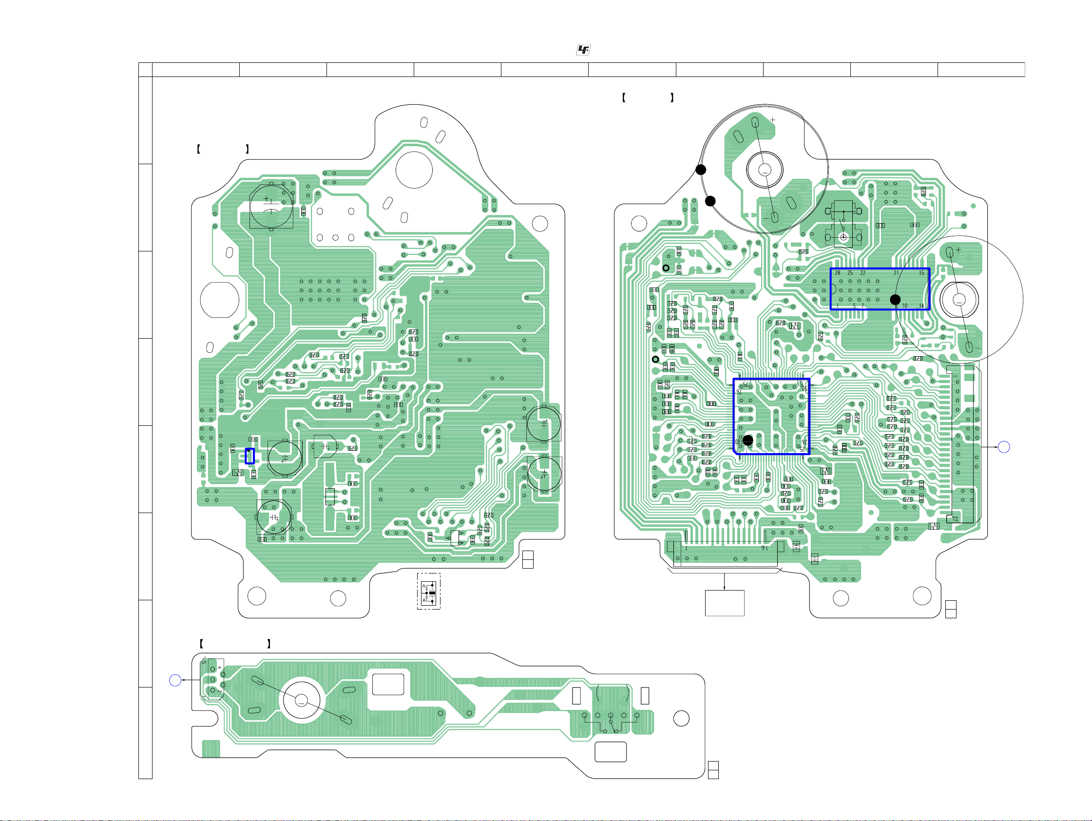
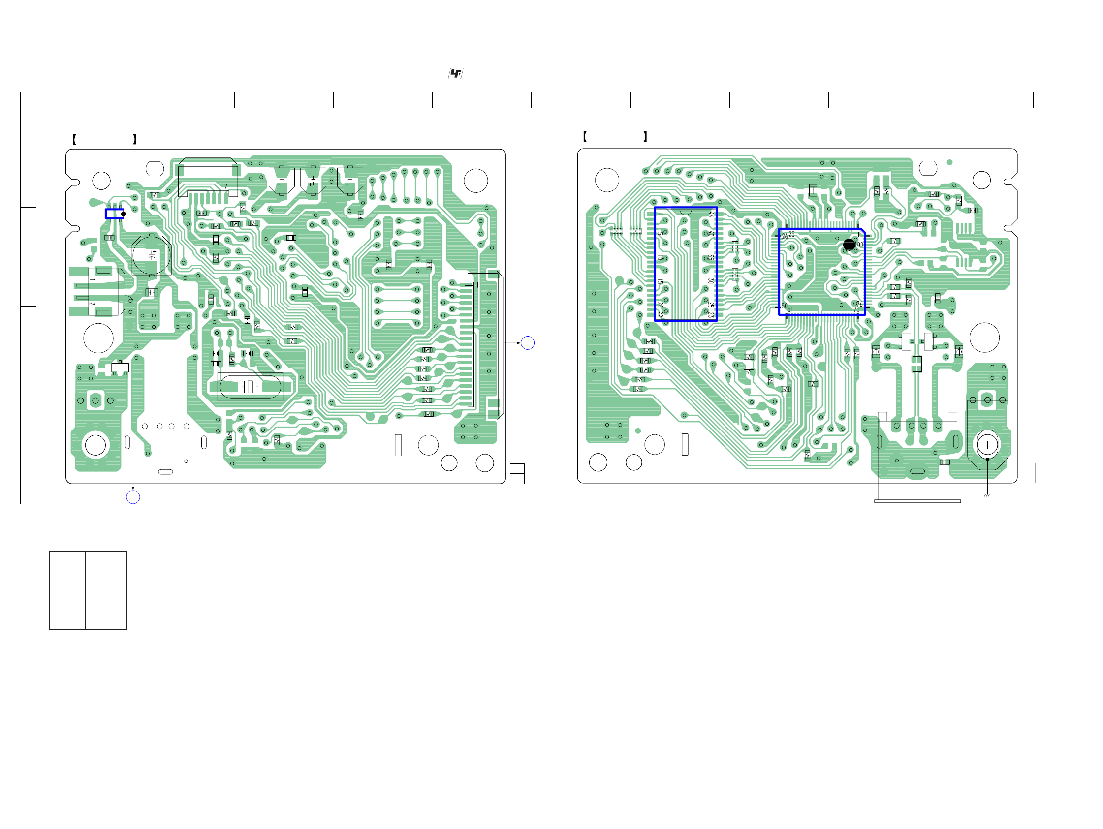
6-6. PRINTED WIRING BOARDS - CD Section -
12345678910
A
CD BOARD (COMPONENT SIDE)
C401
B
C405
C
R415
R213
C202
C201
R216
R121
R211
C206
R201
C212
C207
135
4
C205
C204
D
IC201
E
C115
X102
R112
R111
R212
R214
C133
F
• See page 21 for Circuit Boards Location.
R118
C153
R114
C108
R119
C112
R155
C130
R302
R303
R304
R301
C307
1-872-620-
C128
E
Q301
C309
X102
• : Uses unleaded solder.
CD BOARD (CONDUCTOR SIDE)
M401
(SLED)
C125
C124
TP124(VC)
C122
R140
C123
R142
R143
C143
C141
C144
C148
C137
C138
C139
C140
C142
R144
C146
C147
C149
R148
C150
R151
TP121
(RFI)
C106
C306
11
(11)
R136
R135
R146
C145
R134
C118
R139
R145
R147
R149
R150
R128
R130
C100
C105
C104
C117
CN301
R129
C136
C135
C120
C107
C119
M
IC101
C102
C101
C103
R101
C126
C127
C113
R109
C303
R108
R102
R106
C301
R402
R105
C302
R414
C109
R104
C132
(LIMIT)
C110
S201
R154
R405
C404
C403
IC401
M
R408
R224
R210
R209
R110
R218
R219
R220
R221
R153
R222
C116
R223
R157
R156
C217
R208
R207
R206
R205
R204
R203
CN202
C151
C152
R202
M402
(SPINDLE)
A
MAIN BOARD
CN701
(Page 30)
G
MOTOR BOARD
R
MAIN BOARD
CN720
(Page 30)
H
HCD-HX50BTR/HX70BTR/HX80R/HX90BTR
CN001
M
M001
(LOADING)
OPTICAL PICK-UP
S001
DISC TRAY
OPEN/CLOSE
DETECT
OPEN5CLOSE
1-866-548-
BLOCK
(KSM-213DCP)
21
(21)
1-872-620-
11
(11)
2222
HCD-HX50BTR/HX70BTR/HX80R/HX90BTR
HCD-HX50BTR/HX70BTR/HX80R/HX90BTR
2323
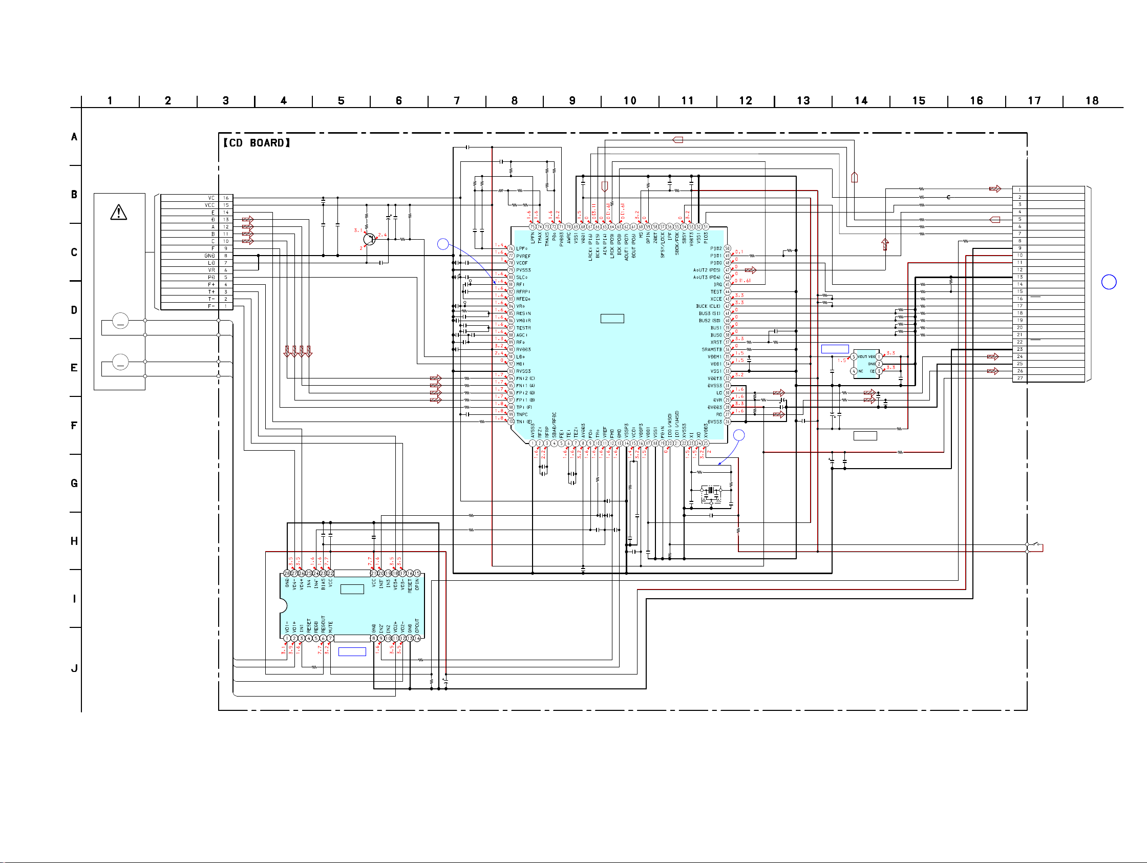
6-7. SCHEMATIC DIAGRAM - CD Board -
• See page 28 for Waveforms. • See page 44 for IC Block Diagrams. • See page 50 for IC Pin Function Description.
IC B/D
A
MAIN
BOARD
(3/3)
CN701
2
1
IC B/D
OPTICAL
PICK-UP
BLOCK
(KSM-213DCP)
M
M
CLOCK
GATE
ST_REQ
GPIN/AIN
SF SY/BCKIN
ZDET/LRCKIN
M-MUTE
MGND
VM (7V)
DVDD (3.3V)
D-OUT
DGND
SBSY
REQ
BUCK
BUS3
BUS2
BUS1
BUS0
AGND
DACGND
AVDD (3.3V)
L-OUT
R-OUT
CCE
DATA
R224 100
R121
100
R108
R109 100
R154
R153
C201
R304
R201
R110
R303
R203
R204
R205
R206
R207
R208
R209
R210
R219
R223
R222
R221
R218
R112
R202
R211
Q301
R301
C202
R157
TP121 (RFI)
TP124 (VC)
R156
CN301
R101
C401
R415
R102
R128
R129
R143
R142 R139
R114
R140
R151
R220
R150
R212
IC101
R105
R106
IC201
X102
C301
C307
C309
C100
C138
C153
C151
C204
C130
C128
C113
C127
C126
C103
C102
C120
C118
C117
C101
C124
C125
R145
R146
R147
R148
R149
C149
C105
C143
C146
C145
C148
C104
C405
C404
C403
C205
C116
C133
CN202
C110
R111
C115
R155
C109
C132
R104
C123
C122
C139
C150
R136 R135
R134
C112 C108
R119
R118
C136
C107
R130
R144
C144
C147
C140
C137
C141
C142
C106
R302
C306
C303C302
R405
R402
R408
R414
C207
C152
C206
IC401
1M
1M
100
10V
2.2
0
10k
C212
100k
2.2
100
100
100
100
100
100
100
100
100k
100k
100k
100k
100k
100
0
100
2SA2119K
100k
100
10V
100
100
16P
220
220
10V
47k
10k
470k
1k
47k
22k 47k
10k
0
0
100k
0
TK63115SCL-G@GT
0.1
1
0.001
0.1
470p
0.0022
0.1
0.1
0.0022
0.1
0.1
0.1
0.01
0.01
0.022
C119
0.022
0.1
0.0047
0.0047
0
0
0
0
0
22p
0.1
0.01
470p
0.01
47p
0.1
0.1
0.1
0.1
0.1
0.1
0.1
0.1
100
22
6.3V
47
0.1
0.1
0
470p
470p
0.01
0.001
22k 470k
1M
0.1 0.1
47p
0.1
4.7k
22k
0.1
0.1
0.01
0.01
0.0022
0.1
100
10V
0
100
10V
1010
10k
2.2k
2.2k
4.7k
1
0.0022
1
BA5826SFP-E2
SP-
SP+
SL+
SL-
100
R213 100
R214 100
R216
100
1M
1k
16.9344MHz
TC94A70FG-101
5p
5p
27P
0
100k
IC101
CD-MP3 PROCESSOR
IC401
FOCUS/TRACKING COIL DRIVE,
SLED/SPINDLE MOTOR DRIVE
IC201
+1.5V REGULATOR
SPSP+
SL+
SL-
M401
(SPINDLE)
M402
(SLED)
AUTOMATIC POWER
CONTROL
S201
(LIMIT)
0.1
C217
100k
RST
(Page
33)
HCD-HX50BTR/HX70BTR/HX80R/HX90BTR
6-8. PRINTED WIRING BOARD - USB Board -
1 2 3 4 5 6 7 8 9 10
USB BOARD (COMPONENT SIDE)
C901
C910
C912
(NC)
CN904
R901
R938
R937
C915
R934
C913
R922
R919
X901
R913
A
R928
31
IC915
45
C916
B
CN908
C
A/K
D905
A
C917
C918
K
D
MAIN BOARD
C
CNA506
(Page 30)
• See page 21 for Circuit Boards Location.
C909
R983
C908
C902
R986
R915
C907
R981
R985
C906
C903
C904
C905
C922
R978
R979
R932
R977
R982
R984
R976
• : Uses unleaded solder.
C921
(22)
MAIN BOARD
B
(Page 30)
22
CN907
21
1-872-405-
CN751
USB BOARD (CONDUCTOR SIDE)
RB922 RB921
IC921
R975
R974
R973
R972
R971
R970
RB924
RB923
R941
R902
R942
R943
R904
R903
R944
R907
IC901
R905
JR902
R906
R916
R949
R917
FB901
R933
R924
R923
R947
R921
R945
R926
C920
R925
A
A/K
D902
D901
A/K
K
L901
CN902
(USB)
C930
R920
C914
K
FB902
A
EP901
14
22
1-872-405-
(CHASSIS)
(22)
• Semiconductor
Location
Ref. No. Location
D901 C-9
D902 C-10
D905 C-1
IC901 B-8
IC915 B-1
IC921 B-7
HCD-HX50BTR/HX70BTR/HX80R/HX90BTR
2424

HCD-HX50BTR/HX70BTR/HX80R/HX90BTR
HCD-HX50BTR/HX70BTR/HX80R/HX90BTR
2525
6-9. SCHEMATIC DIAGRAM - USB Board -
• See page 28 for Waveforms. • See page 44 for IC Block Diagrams. • See page 50 for IC Pin Function Description.
R970
R971
R972
R973
R974
R975
R976
R977
R979
R978
R932
R982
R984
RB922
RB921
RB923
RB924
C907
C906
C921
R901
C901
R937
R983
C902
JR902
C903
C922
R907
R906
R905
R904
R903
R902
R917
R915
R913
C908
R919
C909
R916
C910C912
R944
R943
R942
R941
C905
C904
R933
R934
R938
C915
C913
C914
R981
R922
R924
R923
R921
IC921
CN904
R926
R925C920
IC915
C916
R920
CN907
CN902
EP901
CN908
FB901
C930
D905
D902
C918C917
IC901
R928
D901
X901
R949
100
100
100
100
100
100
100
100
100
100
100
100
100
47
47
47
47
0.1
0.1
0.1
10k
0.1
100
100
10
16V
0
10
16V
0.1
4.7k
4.7k
4.7k
4.7k
4.7k
4.7k
0
10k
100k
0.1
100
22p
0
22p10p
100k
100k
100k
100k
0.1
10
16V
0
R945 4.7k
R947 4.7k
10k
100
0.1
0.1
0.1
100
R985 100
R986 100
100k
27
27
100k
IS61LV6416-10T
7P
15k
15k0.1
R5523N001BTR-F
0.1
10k
21P
4P
2P
0.1
0
9MHz
4.7k
A13
A14
A15
D0
D1
D2
D3
D4
D5
D6
D7
RD
WR
LB
UB
SRAM-CS
A8
A9
A10
D7
D4
D5
D6
WR
D0
D1
D2
D3
SRAM-CS
A11
A12
A13
A14
A15
LB
UB
RD
A7
A8
A9
A10
A11
A12
A4
A5
A6
D12
D13
D14
D15
A4
A5
A6
D8
D9
D10
D11
D12
D13
D14
D15
BUS0
BUS1
BUS2
BUS3
BUCK
CCE
USB-SI
USB-SO
DO
DATA
CLOCK
USB-RST
LRCK
BCK
REQ
ST-REQ
A-IN
GATE
LRCK
CCE
BUCK
BUS3
BUS2
BUS1
BUS0
DO
DI
USB-SO
USB-SI
DATA
CLOCK
BCK
A-IN
GATE
REQ
ST-REQ
USB-RST
DI
A7
A16
A16
A1
A2
A3
A1
A2
A3
D11
D10
D9
D8
BOOT
AMO
TXD1
RXD1
RESET
BOOT
AM0
TXD1
RXD1
RESET
EN
FLG
EN
FLG
MC2837
MC2837
10220
6.3V
TMP92CD28AFG-6VD8
MC2837
D+
DAM0
DVSS
DVSS
RVOUT1
RVIN
RVIN
RVOUT2
DVSS
DVSS
DVSS
AM1
X2
DVSS
X1
VBUS-5V
DVDD 3.3V
DVSS
LRCK
CCE
BUCK
BUS3
BUS2
BUS1
BUS0
USB-RST
ST-REQ
REQ
GATE
A-IN
BCK
VBUS-GND
BOOT
RESET
RXD1
TXD1
DVSS
VCC
AM0
CLOCK
DATA
USB-SI
DO
DI
USB-SO
NC
A6
A5
A4
A3
NC
I/O8
I/O10
I/O11
VDD
GND
I/O12
I/O13
I/O14
I/O15
A2
A1
A0
I/O9
NC
A7
A8
A9
A10
I/O7
I/O6
I/O5
I/O4
GND
VDD
I/O3
I/O2
I/O1
I/O0
A11
A12
A13
A14
A15
WE
CELB
UB
OE
A13
GND
D+
D-
VBUS
(CHASSIS)
EN
GND
OUT
INFLG
(USB)
(NC)
S-RAM
VBUS POWER ON/OFF SWITCH
A12
A11
A10
A9
A8
DVCC
A7
A6
A5
A4
A3
A2
A1
A0
D15
D14
D13
D12
D11
D10
D9
D8
DVCC
D7
D6
D5
D4
D3
S2
D1
D0
DVSS
DVCC
DVCC
DVSS
NO USE
NO USE
NO USE
DVCC
G-3
NO USE
NO USE
DI
G-2
G-1
ST-REQ
REQ
DVCC
GATE
DATA
BCK
SCL
SDA
NO USE
RXD1
TXD1
CLOCK
DATA
DO
NO USE
USBPON
USBOC
DVCC
BOOT
NO USE
SRLUB
SRLLB
RD
WR
CS2
DVCC
NO USE
/CCE
/BUCK
BUS3
BUS2
BUS1
BUS0
A16
A15
A14
USB CONTROLLER
LRCK
/RESET
0
FB902
0
L901
(Page
33)
(Page 32)
 Loading...