

Sony HCD-HX3, HCD-HX5, HCD-HX7 Schematic
HCD-HX3/HX5/HX7
SERVICE MANUAL
Ver. 1.0 2007.03
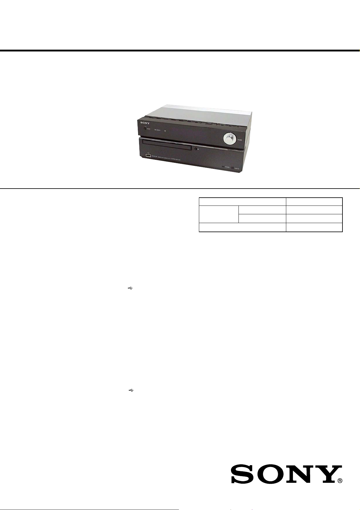
• HCD-HX3 is the amplifier, USB, CD player
and tuner section in CMT-HX3.
• HCD-HX5 is the amplifier, bluetooth, USB,
CD player and tuner section in CMT-HX5BT.
• HCD-HX7 is the amplifier, bluetooth, CD
player and tuner section in CMT-HX7BT.
• The Bluetooth word mark and logos are owned by the Bluetooth SIG, Inc.
and any use of such marks by Sony Corporation is under license. Other
trademarks and trade names are those of their respective owners.
• “WALKMAN” and “WALKMAN” logo are registered trademarks of Sony Corporation.
• MICROVAULT is a trademark of Sony Corporation.
• ATRAC, ATRAC3, ATRAC3plus and their logos are trademarks of Sony Corporation.
• U.S. and foreign patents licensed from Dolby Laboratories.
• MPEG Layer-3 audio coding technology and patents licensed from
Fraunhofer IIS and Thomson.
• The XM name and related logos are registered trademarks of XM Satellite Radio Inc.
• (c) 2006 SIRIUS Satellite Radio Inc. “SIRIUS” and the SIRIUS dog logo
are registered trademarks of SIRIUS Satellite Radio Inc.
TM ®
• and marks are omitted in this manual.
Photo: HCD-HX3
US Model
HCD-HX7
Canadian Model
AEP Model
HCD-HX3/HX5
UK Model
Australian Model
Korean Model
HCD-HX5
Model Name Using Similar Mechanism NEW
Base Unit Name HCD-HX7 BU-K6BD90-WOD
HCD-HX3/HX5 BU-K6BD90U-WOD
Optical Pick-Up Block Name KSM-213DCP
– HCD-HX7 –
AUDIO POWER SPECIFICATIONS
POWER OUTPUT AND TOTAL
HARMONIC DISTORTION:
(The United States model only)
With 6 ohm loads, both channels driven,
from 120 – 10,000 Hz; rated 50 watts per
channel minimum RMS power, with no
more than 10% total harmonic distortion
from 250 milliwatts to rated output.
Amplier section
– HCD-HX7 –
Continuous RMS power output
(reference): 50 + 50 watts (6 ohms at
1 kHz, 10% THD)
Inputs:
AUDIO IN (stereo mini jack):
voltage 250 mV, impedance 47
kilohms
Outputs:
PHONES (stereo mini jack): accepts
headphones of 8 ohms or more
SPEAKER: accepts impedance of
6 ohms
– HCD-HX5 –
Canadian, Australian, Korean models:
DIN power output (rated):
60 + 60 watts (4 ohms at 1 kHz, DIN)
Continuous RMS power output
(reference): 75 + 75 watts (4 ohms at
1 kHz, 10% THD)
European model:
DIN power output (rated):
60 + 60 watts (4 ohms at 1 kHz, DIN)
Continuous RMS power output
(reference): 75 + 75 watts (4 ohms at
1 kHz, 10% THD)
Music power output (reference):
75 + 75 watts (4 ohms at 1 kHz, 10%
THD)
Inputs:
AUDIO IN (stereo mini jack):
voltage 250 mV, impedance 47
kilohms
(USB) port: Type A, maximum
current 500 mA
Outputs:
PHONES (stereo mini jack): accepts
headphones of 8 ohms or more
SPEAKER: accepts impedance of
4 ohms
– HCD-HX3 –
Canadian model:
DIN power output (rated): 40 + 40
watts (6 ohms at 1 kHz, DIN)
Continuous RMS power output
(reference): 50 + 50 watts (6 ohms at
1 kHz, 10% THD)
European model:
DIN power output (rated): 40 + 40
watts (6 ohms at 1 kHz, DIN)
Continuous RMS power output
(reference): 50 + 50 watts (6 ohms at
1 kHz, 10% THD)
Music power output (reference): 50 +
50 watts (6 ohms at 1 kHz, 10% THD)
Inputs:
AUDIO IN (stereo mini jack):
voltage 250 mV, impedance
47 kilohms
(USB) port: Type A, maximum
current 500 mA
Outputs:
PHONES (stereo mini jack): accepts
headphones of 8 ohms or more
SPEAKER: accepts impedance of
6 ohms
SPECIFICATIONS
Bluetooth section (HCD-HX5/HX7)
Communication system:
Bluetooth Standard version 2.0
Output:
Bluetooth Standard Power Class 2
Maximum communication range:
Line of sight approx. 10 m
Frequen cy band:
2.4 GHz band (2.4000 GHz –
2.4835 GHz)
Modulation method:
FHSS
Compatible Bluetooth proles
A2DP (Advanced Audio Distribution
Profile)
AVRCP (Audio Video Remote
Control Profile)
Supp or ted codecs:
Receive: SBC (Sub Band Codec), MP3
Transmit: SBC (Sub Band Codec)
1)
The actual range will vary depending on
factors such as obstacles between devices,
magnetic fields around a microwave oven,
static electricity, reception sensitivity,
antenna’s performance, operating system,
software application, etc.
2)
Bluetooth standard proles indicate the
purpose of Bluetooth communication
between devices.
USB section (HCD-HX3/HX5)
Supported bit rate
MP3 (MPEG 1 Audio Layer-3):
32 – 320 kbps, VBR
ATRAC: 48 – 352 kbps
(ATRAC3plus), 66/105/132 kbps
(ATRAC3)
WMA: 32 – 192 kbps, VBR
AAC: 48 – 320 kbps
Sampling frequencies
MP3 (MPEG 1 Audio Layer-3):
32/44.1/48 kHz
ATRAC: 44.1 kHz
WMA: 44.1 kHz
1)
2)
:
AAC: 44.1 kHz
CD player section
System: Compact disc and digital audio
system
Laser Diode Properties
Emission duration: continuous
Laser Output*: Less than 44.6µW
* This is output is the value measurement
at a distance of 200mm from the
objective lens surface on the Optical
Pick-up Block with 7mm aperture.
Frequency response: 20 Hz – 20 kHz
Signal-to-noise ratio: More than 90 dB
Dynamic range: More than 90 dB
Tuner section
FM stereo, FM/AM superheterodyne tuner
FM tuner section:
Tuning range
US, Canadian models: 87.5 – 108.0 MHz
(100 kHz step)
Other models: 87.5 – 108.0 MHz
(50 kHz step)
Antenna: FM lead antenna
Antenna terminals: 75 ohms unbalanced
Intermediate frequency: 10.7 MHz
– Continued on next page –
9-887-618-01
2007C05-1
© 2007.03
COMPACT DISC RECEIVER
Sony Corporation
Personal Audio Division
Published by Sony Techno Create Corporation
HCD-HX3/HX5/HX7
r
AM tuner section:
Tun ing range
US, Canadian models:
530 – 1,710 kHz (with 10 kHz tuning
interval)
531 – 1,710 kHz (with 9 kHz tuning
interval)
European model:
531 – 1,602 kHz (with 9 kHz tuning
interval)
Other models:
530 – 1,710 kHz (with 10 kHz tuning
interval)
531 – 1,602 kHz (with 9 kHz tuning
interval)
Antenna: AM loop antenna, external
antenna terminal
Intermediate frequency: 450 kHz
General
Power requirements
US, Canadian models: 120 V AC, 60 Hz
Other models: 220 – 240 V AC,
50/60 Hz
Power consumption: 40 watts (HCD-HX3/HX7)
Dimensions (w/h/d) (excl. speakers):
Approx. 285 × 120 × 215 mm
Mass (excl. speakers): 2.6 kg (HCD-HX3/HX7)
Design and specications are subject to
change without notice.
50 watts (HCD-HX5)
2.7 kg (HCD-HX5)
Notes on chip component replacement
• Never reuse a disconnected chip component.
• Notice that the minus side of a tantalum capacitor may be
damaged by heat.
Flexible Circuit Board Repairing
• Keep the temperature of the soldering iron around 270 ˚C
during repairing.
• Do not touch the soldering iron on the same conductor of the
circuit board (within 3 times).
• Be careful not to apply force on the conductor when soldering
or unsoldering.
CAUTION
Use of controls or adjustments or performance of procedures
other than those specified herein may result in hazardous radiation
exposure.
SAFETY CHECK-OUT
After correcting the original service problem, perform the following
safety check before releasing the set to the customer:
Check the antenna terminals, metal trim, “metallized” knobs, screws,
and all other exposed metal parts for AC leakage.
Check leakage as described below.
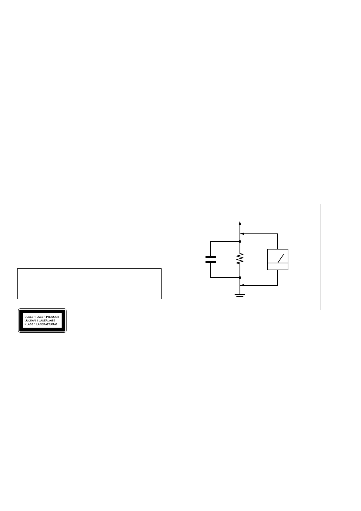
LEAKAGE TEST
The AC leakage from any exposed metal part to earth ground and
from all exposed metal parts to any exposed metal part having a
return to chassis, must not exceed 0.5 mA (500 microamperes.).
Leakage current can be measured by any one of three methods.
1. A commercial leakage tester, such as the Simpson 229 or RCA
WT -540A. Follow the man ufacturers’ instructions to use these
instruments.
2. A battery-operated A C milliammeter . The Data Precision 245
digital multimeter is suitable for this job.
3. Measuring the voltage drop across a resistor by means of a
VOM or battery-operated A C voltmeter . The “limit” indication
is 0.75 V, so analog meters must have an accurate low-v oltage
scale. The Simpson 250 and Sanwa SH-63Trd are examples
of a passive VOM that is suitable. Nearly all battery operated
digital multimeters that have a 2 V AC range are suitable. (See
Fig. A)
To Exposed Metal
Parts on Set
AC
0.15 µF
1.5 k
Ω
voltmete
(0.75 V)
Earth Ground
Fig. A. Using an AC voltmeter to check AC leakage.
This is appliance is classied as a CLASS 1
LASER product. This is marking is located
on the rear exterior.
ATTENTION AU COMPOSANT AYANT RAPPORT
À LA SÉCURITÉ!
LES COMPOSANTS IDENTIFIÉS P AR UNE MARQ UE 0 SUR
LES DIAGRAMMES SCHÉMATIQUES ET LA LISTE DES
PIÈCES SONT CRITIQUES POUR LA SÉCURITÉ DE
FONCTIONNEMENT. NE REMPLACER CES COM- POSANTS
QUE PAR DES PIÈCES SONY DONT LES NUMÉROS SONT
DONNÉS DANS CE MANUEL OU D ANS LES SUPPLÉMENTS
PUBLIÉS PAR SONY.
2
SAFETY-RELATED COMPONENT WARNING!!
COMPONENTS IDENTIFIED BY MARK 0 OR DOTTED LINE
WITH MARK 0 ON THE SCHEMATIC DIAGRAMS AND IN
THE PARTS LIST ARE CRITICAL TO SAFE OPERATION.
REPLACE THESE COMPONENTS WITH SONY PAR TS WHOSE
PART NUMBERS APPEAR AS SHOWN IN THIS MANUAL OR
IN SUPPLEMENTS PUBLISHED BY SONY.

TABLE OF CONTENTS
HCD-HX3/HX5/HX7
1. SERVICING NOTES ............................................... 4
2. GENERAL ................................................................... 5
3. DISASSEMBLY
3-1. Disassembly Flow ........................................................... 9
3-2. Panel (Top) ...................................................................... 10
3-3. Front Panel Block ............................................................ 10
3-4. MAIN Board (HX3/HX5) ............................................... 11
3-5. MAIN Board/XM Board (HX7) ...................................... 11
3-6. Switching Power Board/Sub Power Board...................... 12
3-7. Loading Mechanism Block ............................................. 12
3-8. Base Unit ......................................................................... 13
3-9. BELT ............................................................................... 13
3-10. OP Base Assy (KSM-213D)............................................ 14
4. TEST MODE.............................................................. 15
5. ELECTRICAL CHECKS........................................ 17
6. DIAGRAMS
6-1. Block Diagram – CD SERVO Section – ......................... 18
6-2. Block Diagram
– TUNER/USB/BLUETOOTH Section – ....................... 19
6-3. Block Diagram – MAIN Section – .................................. 20
6-4. Block Diagram – AMP Section – .................................... 21
6-5. Block Diagram
– PANEL/POWER SUPPLY Section – ........................... 22
6-6. Printed Wiring Boards – CD Section – ........................... 24
6-7. Schematic Diagram – CD Section – ............................... 25
6-8. Printed Wiring Boards – USB Section (HX3/HX5) –..... 26
6-9. Schematic Diagram – USB Section (HX3/HX5) – ......... 27
6-10. Printed Wiring Boards
– BLUETOOTH Section (HX5/HX7) –.......................... 28
6-11. Schematic Diagram
– BLUETOOTH Section (HX5/HX7) –.......................... 29
6-12. Printed Wiring Boards – XM Section (HX7) – ............... 30
6-13. Schematic Diagram – XM Section (HX7) – ................... 31
6-14. Printed Wiring Board – MAIN Section –........................ 32
6-15. Schematic Diagram – MAIN Section (1/3) – .................. 33
6-16. Schematic Diagram – MAIN Section (2/3) – .................. 34
6-17. Schematic Diagram – MAIN Section (3/3) – .................. 35
6-18. Printed Wiring Board – AMP Section (HX3/HX7) – ...... 36
6-19. Schematic Diagram – AMP Section (HX3/HX7) –......... 37
6-20. Printed Wiring Board – AMP Section (HX5) – ............... 38
6-21. Schematic Diagram – AMP Section (HX5) – ................. 39
6-22. Printed Wiring Boards – OUTPUT Section – ................. 40
6-23. Schematic Diagram – OUTPUT Section –...................... 40
6-24. Printed Wiring Boards – PANEL Section –..................... 42
6-25. Schematic Diagram – PANEL Section –......................... 43
6-26. Printed Wiring Boards – POWER SUPPLY Section –.... 44
6-27. Schematic Diagram – POWER SUPPLY Section – ........ 45
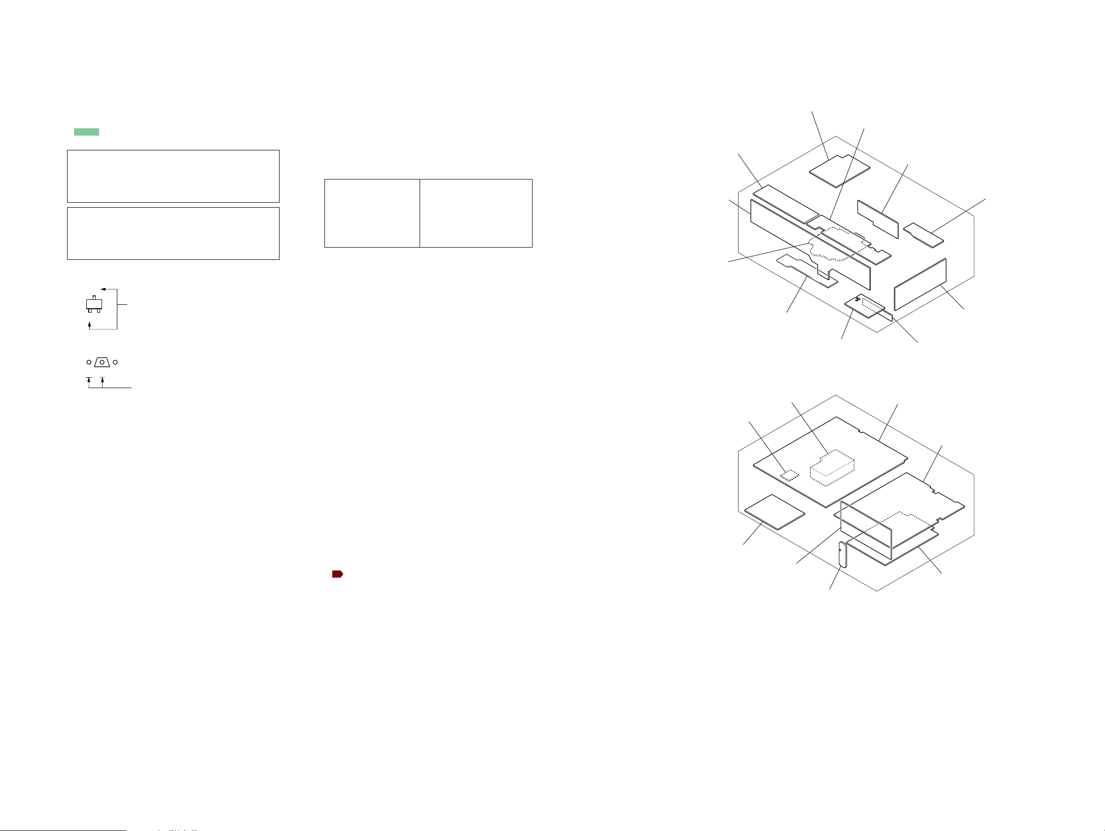
7. EXPLODED VIEWS
7-1. Panel Section ................................................................... 64
7-2. Chassis (Top) Section ...................................................... 65
7-3. Panel Key Section............................................................ 66
7-4. Front Panel Section ......................................................... 67
7-5. MAIN Section ................................................................. 68
7-6. Chassis Section ................................................................ 69
7-7. Loading Mechanism Section ........................................... 70
7-8. Base Unit Section (BU-K6BD90-WOD: HX7)
(BU-K6BD90U-WOD: HX3/HX5) ................................ 71
8. ELECTRICAL PARTS LIST................................ 72
3
HCD-HX3/HX5/HX7
SECTION 1
SERVICING NOTES
NOTES ON HANDLING THE OPTICAL PICK-UP
BLOCK OR BASE UNIT
The laser diode in the optical pick-up block may suffer electrostatic
break-down because of the potential difference generated by the
charged electrostatic load, etc. on clothing and the human body.
During repair, pay attention to electrostatic break-down and also
use the procedure in the printed matter which is included in the
repair parts.
The flexible board is easily damaged and should be handled with
care.
NOTES ON LASER DIODE EMISSION CHECK
The laser beam on this model is concentrated so as to be focused on
the disc reflective surface by the objective lens in the optical pickup block. Therefore, when checking the laser diode emission,
observe from more than 30 cm away from the objective lens.
UNLEADED SOLDER
Boards requiring use of unleaded solder are printed with the leadfree mark (LF) indicating the solder contains no lead.
(Caution: Some printed circuit boards may not come printed with
the lead free mark due to their particular size)
: LEAD FREE MARK
Unleaded solder has the following characteristics.
• Unleaded solder melts at a temperature about 40 °C higher
than ordinary solder.
Ordinary soldering irons can be used but the iron tip has to be
applied to the solder joint for a slightly longer time.
Soldering irons using a temperature regulator should be set to
about 350 °C.
Caution: The printed pattern (copper foil) may peel away if
the heated tip is applied for too long, so be careful!
• Strong viscosity
Unleaded solder is more viscou-s (sticky, less prone to flow)
than ordinary solder so use caution not to let solder bridges
occur such as on IC pins, etc.
• Usable with ordinary solder
It is best to use only unleaded solder but unleaded solder may
also be added to ordinary solder.
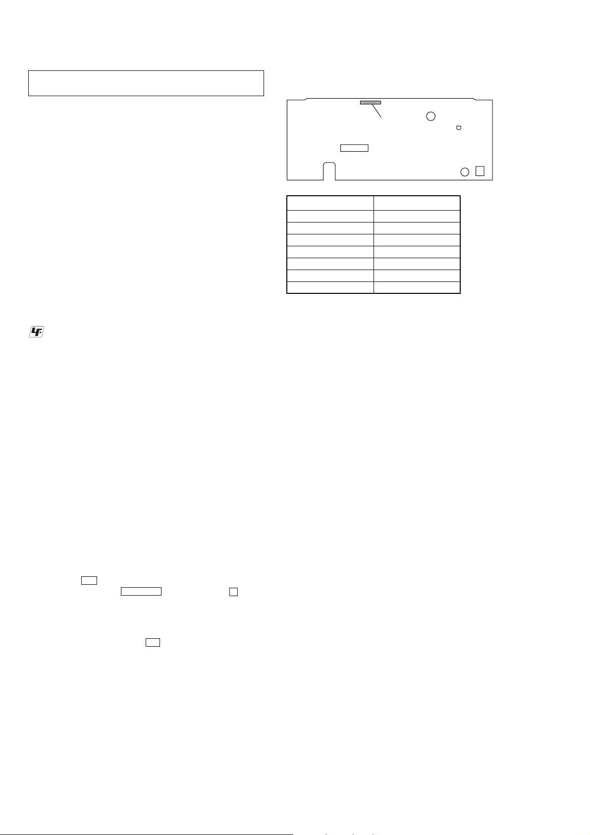
MODEL IDENTIFICATION
– Back Panel –
PART No.
MODEL PART No.
HX3: Canadian 2-895-161-0[]
HX3: AEP 2-895-161-1[]
HX5: Canadian 3-096-225-0[]
HX5: AEP , UK 3-096-225-1[]
HX5: Australian 3-096-225-3[]
HX5: Korean 3-096-225-4[]
HX7 3-096-225-5[]
RELEASING THE ANTITHEFT LOCK
The disc tray lock function for the antitheft of an demonstration
disc in the store is equipped.
Releasing Procedure :
1. Press the I/1 button to turn the power on.
2. While pressing the x/CANCEL button, press the Z button
until “UNLOCKED” displayed on the fluorescent indicator
tube (around 5 seconds).
Note: When “LOCKED” is displayed, the antitheft lock is not released by
turning power on/off with the I/1 button.
4
– HCD-HX3 –
SECTION 2
GENERAL
HCD-HX3/HX5/HX7
This section is extracted from
instruction manual.
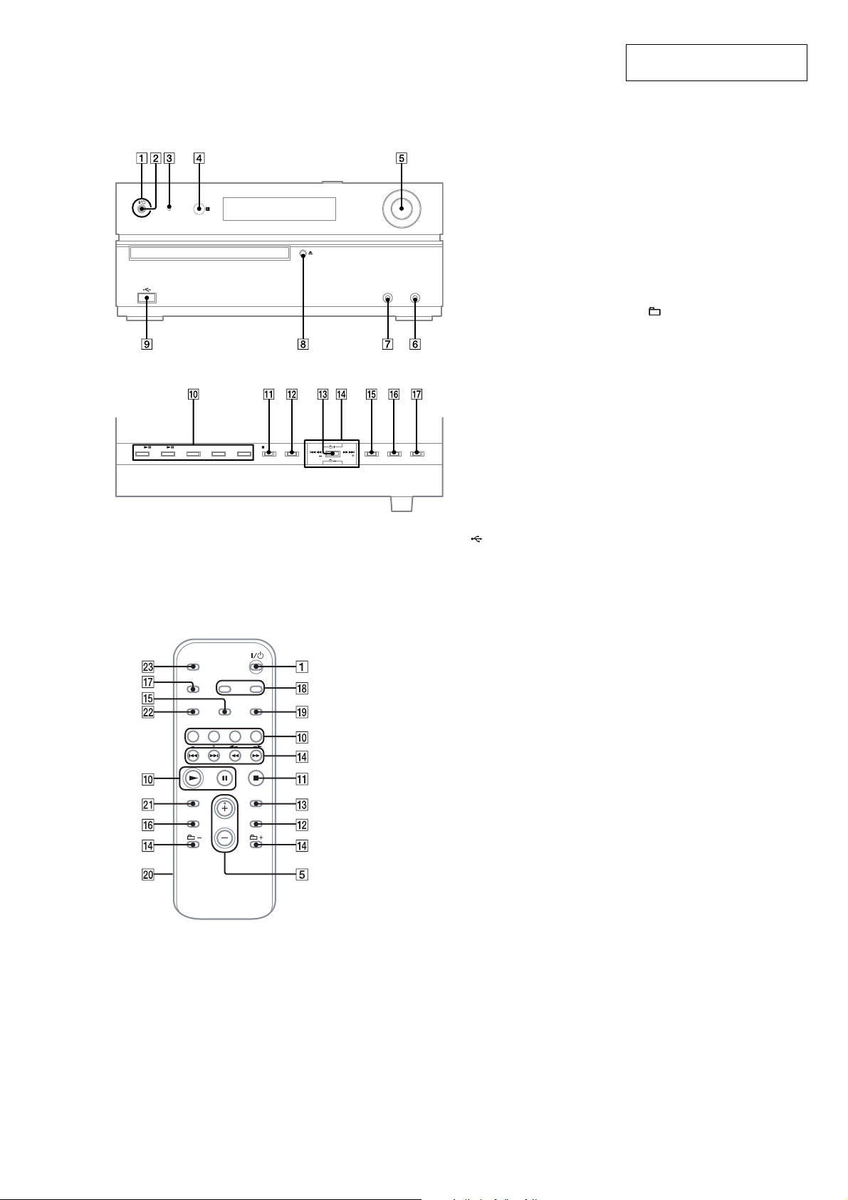
Front panel
Top panel
Remote (RM-SCU35)
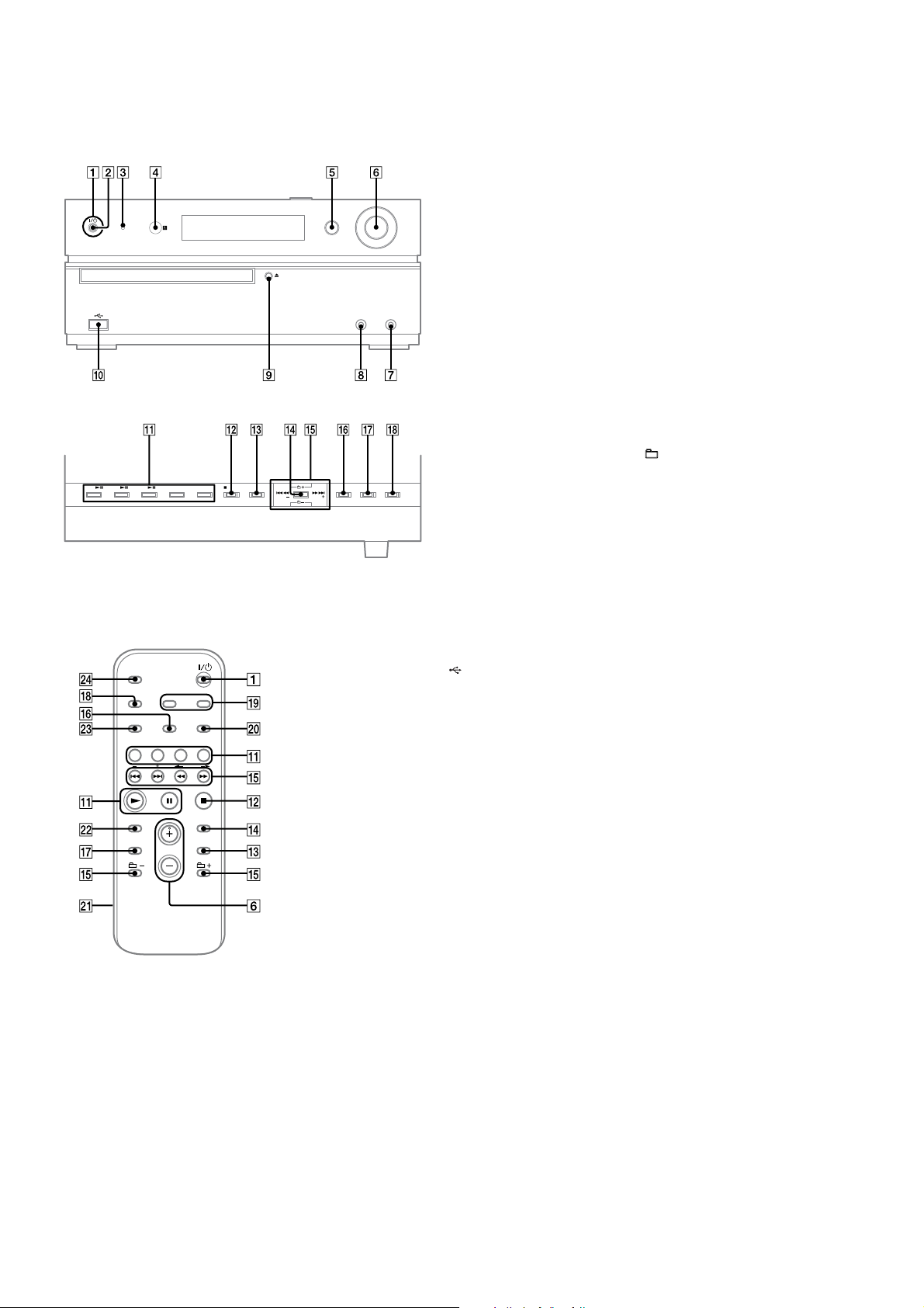
1
"/1 (power) button
Press to turn on the system.
2
STANDBY indicator
Lights up when the system is turned off.
3
USB MEMORY indicator
Lights up when an optional USB device
(Digital music player or USB storage
media) is connected.
4
Remote sensor
5
Unit: VOLUME control
Remote: VOLUME +/– button
Turn or press to adjust the volume.
6
AUDIO IN jack
Connect to an optional audio
component.
7
PHONES jack
Connect the headphones.
8
Z (open/close) button
Press to open or close the disc tray.
9
(USB) port
Connect to an optional USB device
(Digital music player or USB storage
media).
q;
Playback buttons and function
buttons
Unit: USB u (play/pause)
button
Press to select the USB function.
Press to start or pause playback of an
optional USB device (Digital music
player or USB storage media).
Remote: USB button
Press to select the USB function.
Unit: CD u (play/pause)
button
Press to select the CD function.
Press to start or pause playback of a disc.
Remote: CD button
Press to select the CD function.
Remote: N (play) button,
X (pause) button
Press to start or pause playback.
TUNER/BAND button
Press to select the TUNER function.
Press to select FM or AM reception
mode.
Unit: AUDIO IN button
Press to select the AUDIO IN function.
FUNCTION button
Press to select the function.
qa
Unit: x/CANCEL (stop/cancel)
button
Remote: x(stop) button
Press to stop playback.
Press to cancel search.
qs
SEARCH button
Press to enter or exit search mode.
qd
ENTER button
Press to enter the settings.
qf
./> (go back/go forward)
button
Press to select a track or file.
Unit: TUNE +/– (tuning) button
Remote: +/– (tuning) button
Press to tune in the desired station.
+/– (select folder) button
Press to select a folder.
m/M (rewind/fast forward)
button
Press to nd a point in a track or file.
qg
PLAY MODE/TUNING MODE
button
Press to select the play mode of a CD,
MP3 disc or an optional USB device
(Digital music player or USB storage
media).
Press to select the tuning mode.
qh
Sound buttons
Unit: DSGX button
Remote: EQ button
Press to select the sound effect.
qj
DISPLAY button
Press to change the information on the
display.
qk
CLOCK/TIMER SELECT button
CLOCK/TIMER SET button
Press to set the clock and the Play Timer.
ql
REPEAT/FM MODE button
Press to listen to a disc, a single track or
file repeatedly.
Press to select the FM reception mode
(monaural or stereo).
w;
Battery compartment lid
wa
CLEAR button
Press to delete a pre-programmed track
or file.
ws
TUNER MEMORY button
Press to preset the radio station.
wd
SLEEP button
Press to set the Sleep Timer.
5
HCD-HX3/HX5/HX7
– HCD-HX5 –
Front panel
Top panel
Remote (RM-SCU35)
1
"/1(power) button
Press to turn on the system.
2
STANDBY indicator
Lights up when the system is turned off.
3
BLUETOOTH indicator
Lights up when the Bluetooth function
is active.
4
Remote sensor
5
BLUETOOTH OPR button
Press to make a connection,
disconnection, or pairing with a
Bluetooth device.
6
Unit: VOLUME control
Remote: VOLUME +/– button
Turn or press to adjust the volume.
7
AUDIO IN jack
Connect to an optional audio
component.
8
PHONES jack
Connect the headphones.
9
Z (open/close) button
Press to open or close the disc tray.
q;
(USB) port
Connect to an optional USB device
(Digital music player or USB storage
media).
qa
Playback buttons and function
buttons
Unit: BLUETOOTH u (play/
pause) button
Press to select the Bluetooth function.
Press to start or pause playback of the
music on the Bluetooth device (Bluetooth
mobile phone, etc.).
Unit: USB u (play/pause)
button
Press to select the USB function.
Press to start or pause playback of an
optional USB device (Digital music
player or USB storage media).
Remote: USB button
Press to select the USB function.
Unit: CD u (play/pause)
button
Press to select the CD function.
Press to start or pause playback of a disc.
Remote: CD button
Press to select the CD function.
Remote: N (play) button,
X (pause) button
Press to start or pause playback.
TUNER/BAND button
Press to select the TUNER function.
Press to select FM or AM reception
mode.
Unit: AUDIO IN button
Press to select the AUDIO IN function.
Remote: FUNCTION button
Press to select the function.
qs
Unit: x/CANCEL (stop/cancel)
button
Remote: x (stop) button
Press to stop playback.
Press to cancel search.
qd
SEARCH button
Press to enter or exit search mode.
qf
ENTER button
Press to enter the settings.
qg
./> (go back/go forward)
button
Press to select a track or file.
Unit: TUNE +/– (tuning) button
Remote: +/– (tuning) button
Press to tune in the desired station.
+/– (select folder) button
Press to select a folder.
m/M (rewind/fast forward)
button
Press to find a point in a track or file.
qh
PLAY MODE/TUNING MODE
button
Press to select the play mode of a CD,
MP3 disc or an optional USB device
(Digital music player or USB storage
media).
Press to select the tuning mode.
qj
Sound buttons
Unit: DSGX button
Remote: EQ button
Press to select the sound effect.
qk
DISPLAY button
Press to change the information on the
display.
ql
CLOCK/TIMER SELECT button
CLOCK/TIMER SET button
Press to set the clock and the Play Timer.
w;
REPEAT/FM MODE button
Press to listen to a disc, a single track or
file repeatedly.
Press to select the FM reception mode
(monaural or stereo).
wa
Battery compartment lid
ws
CLEAR button
Press to delete a pre-programmed track
or file.
Press to erase the pairing registration
information of the Bluetooth device.
wd
TUNER MEMORY button
Press to preset the radio station.
wf
SLEEP button
Press to set the Sleep Timer.
6
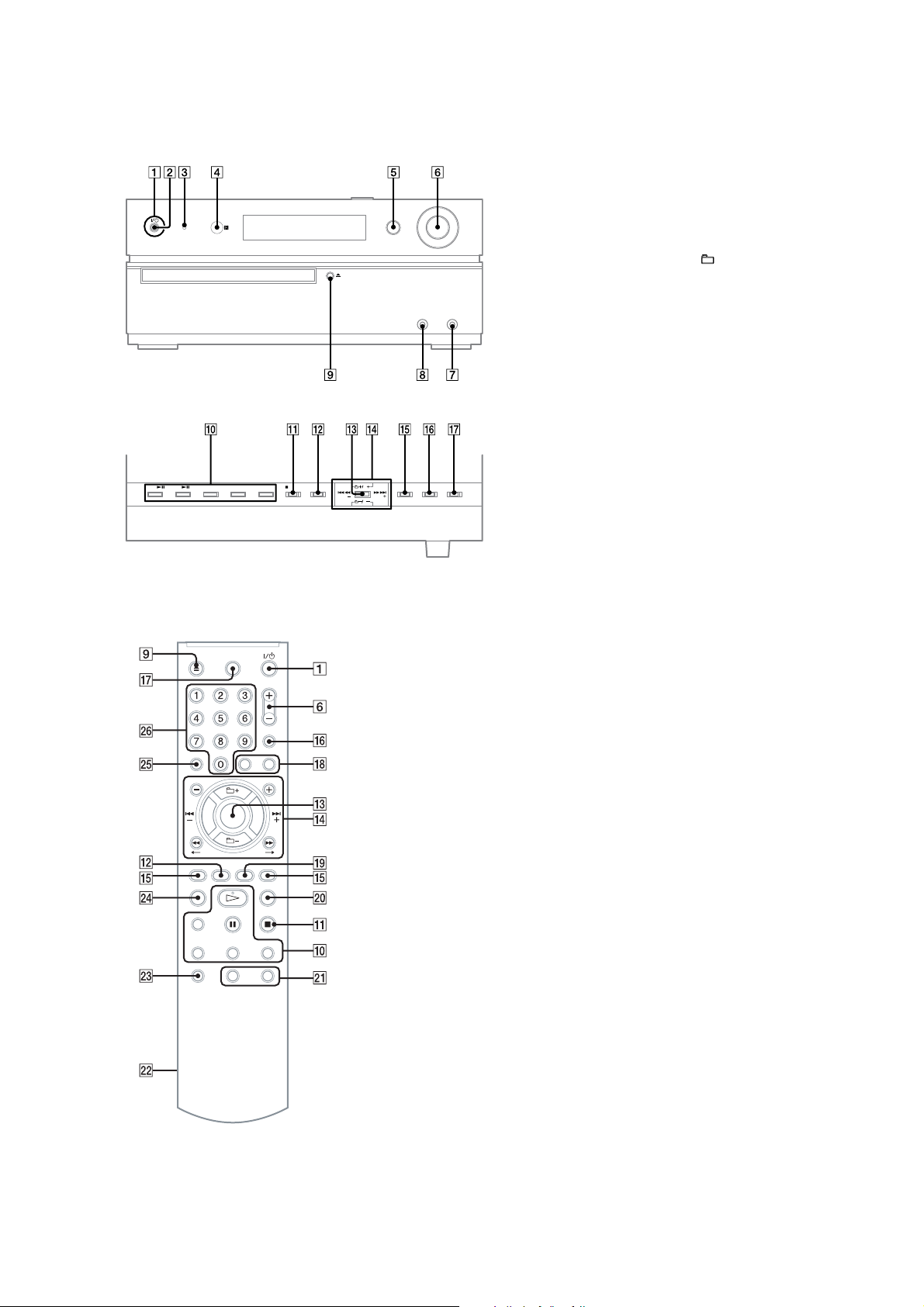
– HCD-HX7 –
Front panel
Top panel
Remote (RM-SCR32)
1
"/1 (power) button
Press to turn on the system.
2
STANDBY indicator
Lights up when the system is turned off.
3
BLUETOOTH indicator
Lights up when the Bluetooth function
is active.
4
Remote sensor
5
BLUETOOTH OPR button
Press to make a connection,
disconnection, or pairing with a
Bluetooth device.
6
Unit: VOLUME control
Remote: VOLUME +/– button
Turn or press to adjust the volume.
7
AUDIO IN jack
Connect to an optional audio
component.
8
PHONES jack
Connect the headphones.
9
Unit: Z (open/close) button
Remote: OPEN/CLOSE Z button
Press to open or close the disc tray.
q;
Playback buttons and function
buttons
Unit: BLUETOOTH u (play/
pause) button
Press to select the Bluetooth function.
Press to start or pause playback of the
music on the Bluetooth device (Bluetooth
mobile phone, etc.).
Unit: CD u (play/pause)
button
Press to select the CD function.
Press to start or pause playback of a disc.
Remote: CD button
Press to select the CD function.
Remote: n (play) button,
X (pause) button
Press to start or pause playback.
TUNER/BAND button
Press to select the TUNER function.
Press to switch among FM, AM, XM and
SIRIUS band.
AUDIO IN button
Press to select the AUDIO IN function.
FUNCTION button
Press to select the function.
qa
Unit: x/CANCEL (stop/cancel)
button
Remote: x(stop) button
Press to stop playback.
Press to cancel search.
qs
SEARCH button
Press to enter or exit search mode.
qd
ENTER button
Press to enter the settings.
HCD-HX3/HX5/HX7
qf
./> (go back/go forward)
button
Press to select a track or file.
Unit: TUNE +/– (tuning) button
Remote: +/– (tuning) button
Press to tune in the desired station.
+/– (select folder) button
Press to select a folder.
Unit: CAT +/– (category) button
Remote: CATEGORY +/– button
Press to select a satellite radio category.
m/M (rewind/fast forward)
button
Press to find a point in a track or file.
qg
PLAY MODE/TUNING MODE
button
Press to select the play mode of a CD or
MP3 disc.
Press to select the tuning mode.
qh
Sound buttons
Unit: DSGX button
Remote: EQ button
Press to select the sound effect.
qj
DISPLAY button
Press to change the information on the
display.
qk
Satellite radio buttons
XM button
Press to select XM band.
SIRIUS button
Press to select SIRIUS band.
ql
TUNER MEMORY button
Press to preset the radio station.
w;
FM MODE button
Press to select the FM reception mode
(monaural or stereo).
wa
CLOCK/TIMER SELECT button
CLOCK/TIMER SET button
Press to set the clock and the Play Timer.
ws
Battery compartment lid
wd
SLEEP button
Press to set the Sleep Timer.
wf
REPEAT button
Press to listen to a disc, a single track or
file repeatedly.
wg
CLEAR button
Press to delete a pre-programmed track
or file.
Press to delete a SIRIUS Parental Lock
password entry.
Press to erase the pairing registration
information of the Bluetooth device.
wh
Number buttons
Press to select a track, file or satellite
channel.
Press to enter a SIRIUS Parental Lock
password.
Press to enter a Bluetooth passcode.
7
HCD-HX3/HX5/HX7
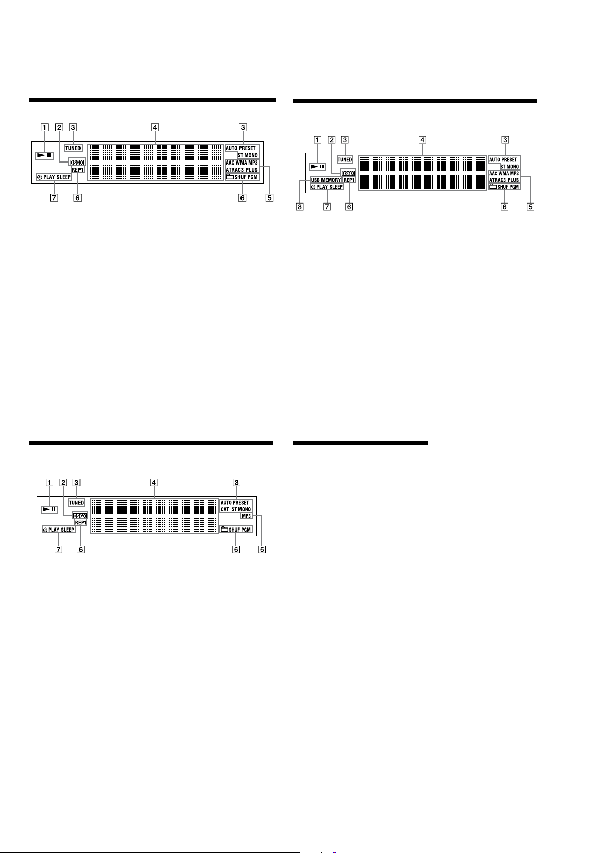
– HCD-HX3 –
Information on the display
1
Play/Pause
2
DSGX
3
Tuner reception mode
Tuner reception
4
Text information
5
Audio format
6
Play mode
7
Timer
– HCD-HX5 –
Information on the display
1
Play/Pause
2
DSGX
3
Tuner reception mode
Tuner reception
4
Text information
5
Audio format
6
Play mode
7
Timer
8
USB MEMORY
Lights up when an optional USB device
is connected.
– HCD-HX7 –
Information on the display
1
Play/Pause
2
DSGX
3
Tuner reception mode
Tuner reception
4
Text information
5
Audio format
6
Play mode
7
Timer
Setting the clock
Use buttons on the remote to set the
clock.
1
Press "/1 to turn on the
system.
2
Press CLOCK/TIMER SET.
If the current mode appears on
the display, press ./>
repeatedly to select “CLOCK SET?”
and then press ENTER.
3
Press ./> repeatedly
to set the hour, and then press
ENTER.
4
Use the same procedure to set
the minutes.
The clock settings are lost when you
disconnect the power cord or if a
power failure occurs.
To display the clock when the system
is off
Press DISPLAY. The clock is displayed
for about 8 seconds.
8
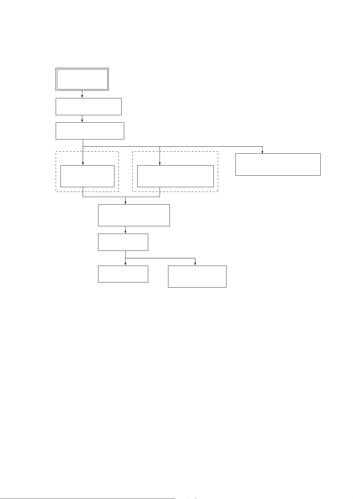
• This set can be disassembled in the order shown below.
3-1. DISASSEMBLY FLOW
SET
3-2. PANEL (TOP)
(Page 10)
3-3. FRONT PANEL BLOCK
(Page 10)
HCD-HX3/HX5/HX7
SECTION 3
DISASSEMBLY
(HX3/HX5)
3-4. MAIN BOARD
(HX3/HX5)
(Page 11)
3-5. MAIN BOARD/XM BOARD
(HX7)
(Page 11)
3-7. LOADING MECHANISM
BLOCK
(Page 12)
3-8. BASE UNIT
(Page 13)
3-9. BELT
(Page 13)
(HX7)
3-10. OP BASE ASSY
(KSM-213D)
(Page 14)
3-6. SWITCHING POWER BOARD/
SUB POWER BOARD
(Page 12)
9
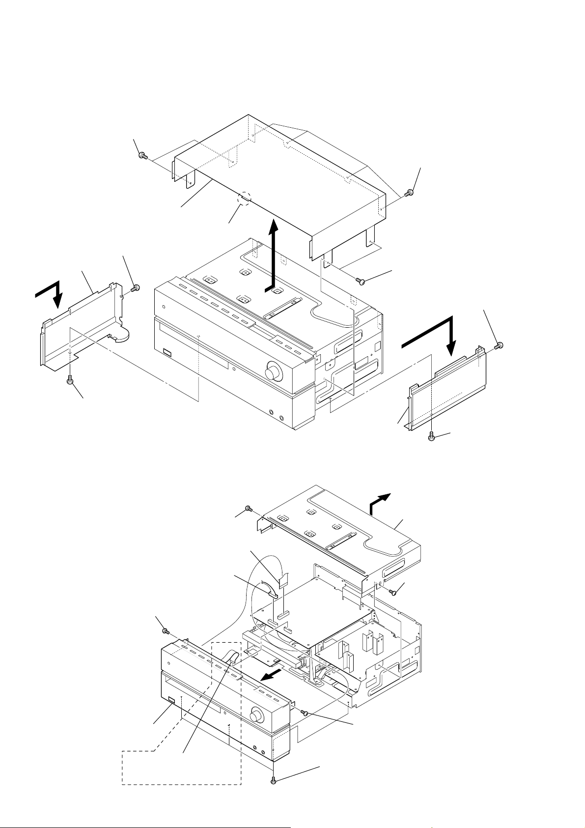
HCD-HX3/HX5/HX7
)
)
Note: Follow the disassembly procedure in the numerical order given.
3-2. PANEL (TOP)
9
two screws
(BVTT3
×
6)
qd
panel (top)
qa
claw
5
screw
(BVTT3
×
6)
8
panel (side L)
qs
9
two screws
(BVTT3
0
four screws
(BVTT3
×
6)
×
6)
7
6
screw
(BVTT3
×
6)
3-3. FRONT PANEL BLOCK
9
3
screw
(BVTT3
×
6)
1
screw
(BVTT3
×
6)
flexible flat cable (17 core)
(CN302)
0
connector
(CN301)
4
panel (side R)
5
6
chassis (top)
2
screw
(BVTT3
1
screw
(BVTT3
×
3
2
6
×
6)
screw
(BVTT3
×
6
10
qs
front panel block
qa
flexible flat cable (15 core)
(CN309)
(HX5/HX7)
8
7
three screws
(BVTP3
4
screw
(BVTT3
×
8)
×
6)
HCD-HX3/HX5/HX7
)
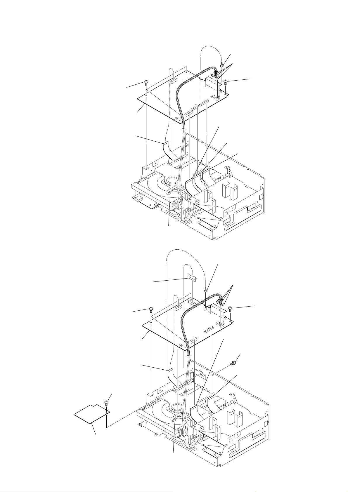
3-4. MAIN BOARD (HX3/HX5)
7
three screws
(BVTT3
×
6)
8
MAIN board
1
flexible flat cable (11 core)
(CN318)
6
connectors
(CN321)
6
three connectors
(CN304, CN305, CN306)
7
screw
(BVTT3
3
flexible flat cable (19 core)
(CN310)
4
flexible flat cable (19 core)
(CN307)
5
flexible flat cable (25 core)
(CN308)
×
6)
2
flexible flat cable (5 core)
(CN320)
3-5. MAIN BOARD/XM BOARD (HX7)
1
flexible flat cable (15 core)
(CN314)
8
three screws
(BVTT3
×
6)
0
MAIN board
2
flexible flat cable (11 core)
(CN318)
qa
screw
(BVTT3
×
6)
7
connector
(CN316)
6
three connectors
(CN304, CN305, CN306)
4
flexible flat cable (19 core)
(CN310)
9
screw
(BVTP3
5
flexible flat cable (25 core
(CN308)
8
screw
(BVTT3
×
8)
×
6)
qs
XM board
3
flexible flat cable (5 core)
(CN320)
11
HCD-HX3/HX5/HX7
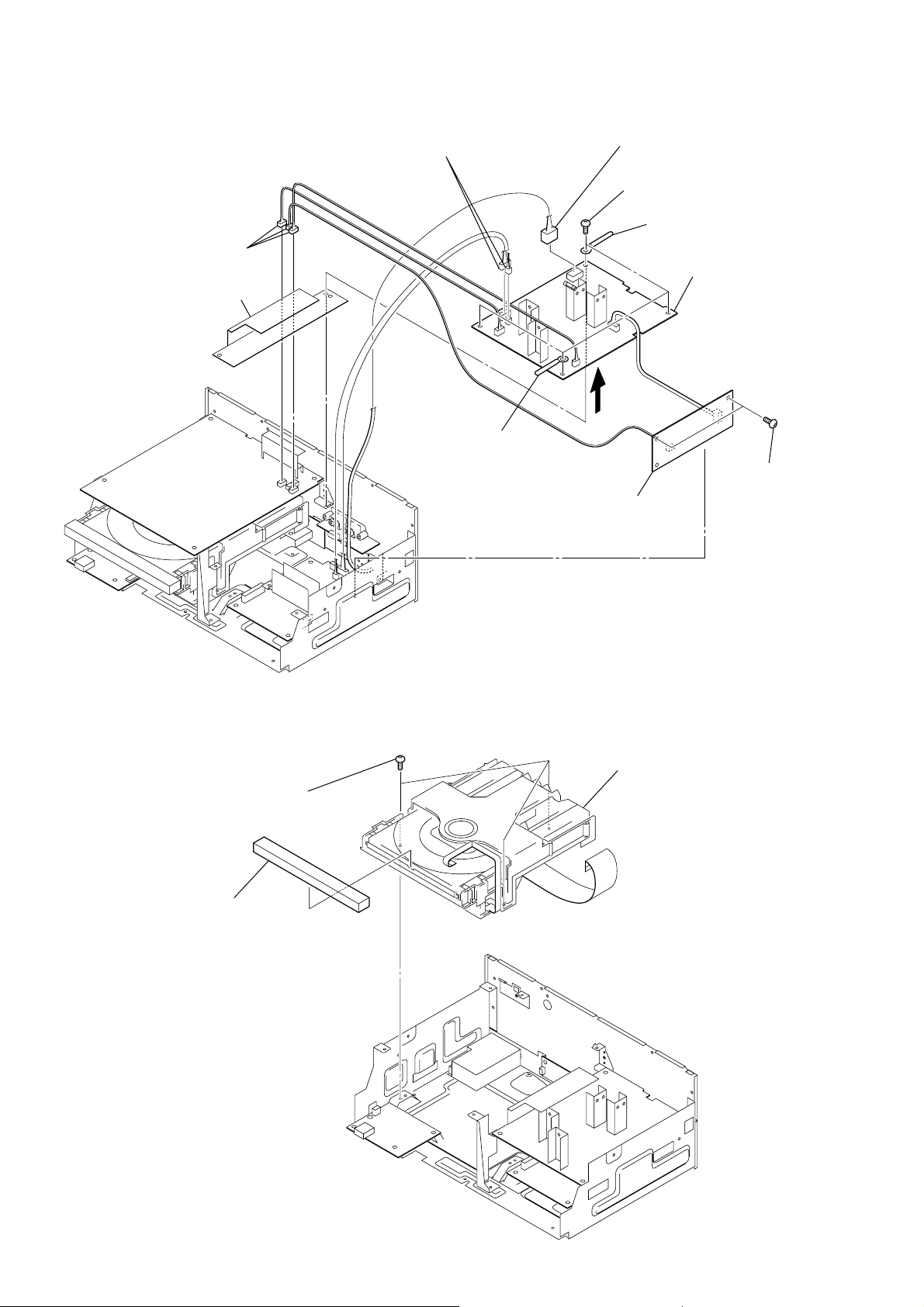
d
k
3-6. SWITCHING POWER BOARD/SUB POWER BOARD
3
two connectors
(CN31, CN33)
1
three connectors
(CN304, CN305, CN306)
9
insulated plate (power)
6
coating clip
2
4
8
qa
SUB POWER board
connector
(CN1)
four screws
(BVTT3
×
6)
5
coating clip
0
SWITCHING POWER boar
7
two screws
(BVTT3
×
6)
3-7. LOADING MECHANISM BLOCK
1
three screws
(BV3)
2
lid (CD) assy
3
loading mechanism bloc
12
3-8. BASE UNIT
1
flexible flat cable
(21 core: HX7) (CN201)
(25 core: HX3/HX5) (CN203)
2
two floating screws
3
two springs (insulator)
2
floating screw
5
insulator
HCD-HX3/HX5/HX7
2
two floating screws
3
two springs
(insulator)
5
insulator
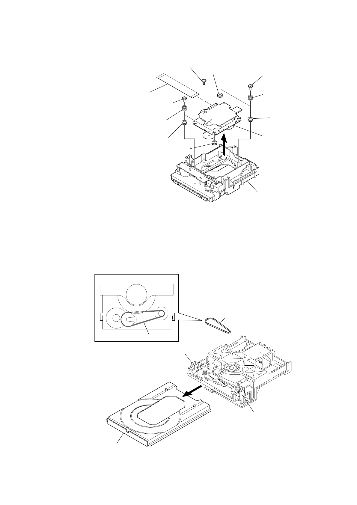
3-9. BELT
position of belt
5
insulator
5
insulator
– Bottom view –
4
6
base unit
loading (BK) assy
3
tray (AU)
belt
2
claw
1
4
belt
2
claw
13
HCD-HX3/HX5/HX7
)
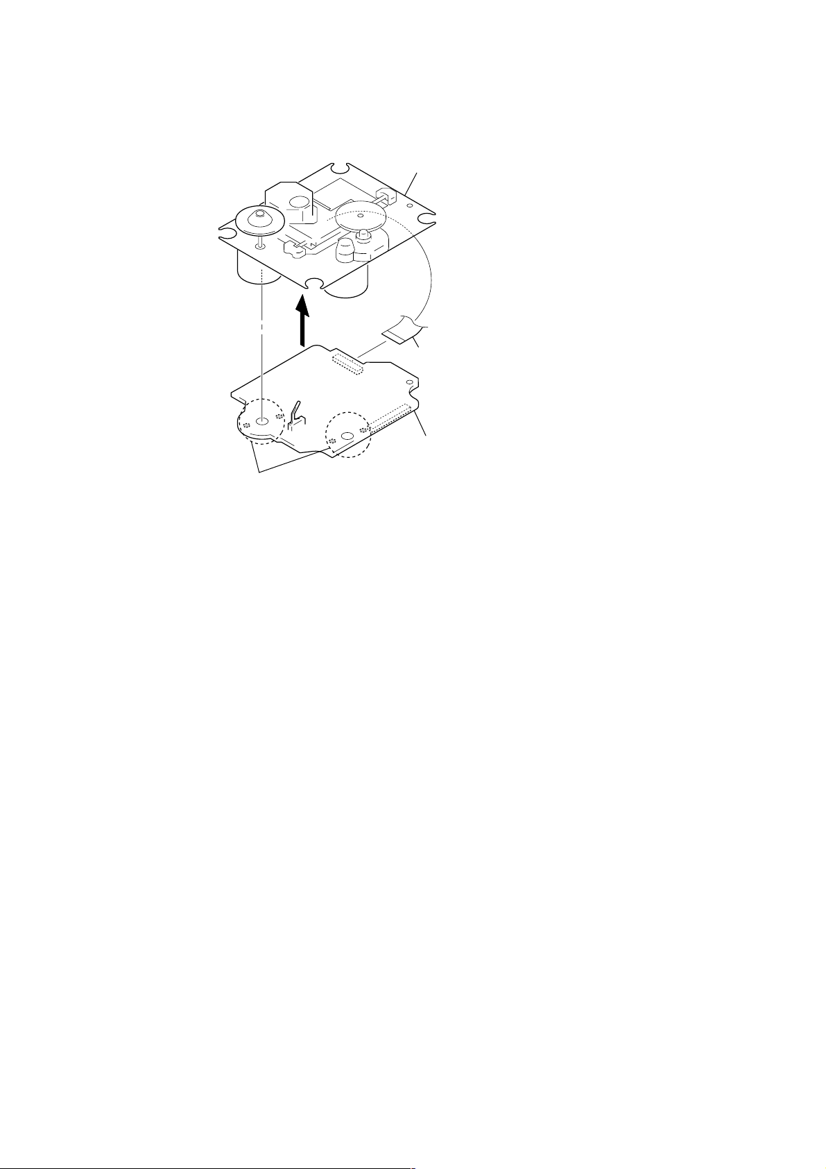
3-10. OP BASE ASSY (KSM-213D)
4
op base assy
(KSM-213D)
1
flexible flat cable (16 core
(CN301)
2
Remove four solders.
3
CD board
14
SECTION 4
TEST MODE
HCD-HX3/HX5/HX7
COLD RESET
The cold reset clears all data including preset data stored in the
RAM to initial conditions. Execute this mode when returning the
set to the customer.
Procedure:
1. Press three buttons of x/CANCEL , [DSGX] and I/1 simultaneously.
2. The system is reset and becomes standby states.
COMMON TEST MODE
This mode is used to check operations of amplifier.
Procedure:
1. Press the I/1 button to turn the power on.
2. Press three buttons of x/CANCEL , [ENTER] and Z simultaneously.
3. When the COMMON test mode is activated, “AUDIO IN” is
displayed on the fluorescent indicator tube and “c PLAY
SLEEP” blink on the fluorescent indicator tube.
4. Each time [EQ] button on the remote commander is pressed,
the display changes starting “TONE MAX”, “TONE MIN”
and “TONE FLAT” this order.
5. Turn the [VOLUME] knob counterclockwise, “V OLUME MIN”
is displayed on the fluorescent indicator tube. Turn the
[VOLUME] knob clockwise, “VOLUME MAX” is displayed
on the fluorescent indicator tube.
6. To release this mode, press the I/1 button.
PANEL TEST MODE
This mode is used to check the fluorescent indicator tube, LED,
model, destination, software version and key.
Procedure:
1. Press the I/1 button to turn the power on.
2. Press three buttons of x/CANCEL , [DSGX] and Z simultaneously.
3. All segments on the fluorescent indicator tube and [STANDBY]
LED light up.
4. Press the [DSGX] button, the model and destination are
displayed on the fluorescent indicator tube.
5. Press the [DSGX] button again, MC version is displayed on
the fluorescent indicator tube.
6. Each time [DSGX] button is pressed, the display changes
starting from MC version, GC version, USBL version (HX3/
HX5 only), USBM version (HX3/HX5 only), BT version
(HX5/HX7 only), CD version, CDD version, CDMA version,
CDMB version, BDA version, BDB version, ST version, TA
version and TM version this order, and returns to the MC
version display.
7. When [SEARCH] button is pressed while the MC version is
displayed, year, month and day of the software creation is
displayed. When [SEARCH] button is pressed again, the display
returns to the MC version display.
8. Press the [ENTER] button, the key test mode is activated
and “K 0 V0” is displayed on the fluorescent indicator tube.
9. Each time a button is pressed, “K” value increases. Howe ver,
once a button is pressed, it is no longer taken into account.
All keys are pressed, display becomes “K17” (HX3) or “K18”
(HX5/HX7).
10. “V” value increases 2, 4, 6 ... if turn the [VOLUME] knob
clockwise, or it decreases 8, 6, 4 ... if turn the knob
counterclockwise
11. To release this mode, press three buttons in the same manner
as step 2, or disconnect the power cord.
TUNER STEP CHANGE
(HX3: Canadian/HX5: Canadian, Australian, Korean/HX7)
A step of AM tuning interval can be changed over between 9 kHz
or 10 kHz.
Procedure:
1. Press the I/1 button to turn the power on.
2. Press the [TUNER/BAND] button to select “AM”.
3. Press the I/1 button again to turn the power off.
4. Press two buttons of [TUNER/BAND] and I/1 simultaneously.
5. The message “AM 9kHz Step” or “AM 10kHz Step” is
displayed on the fluorescent indicator tube and thus the tuning
interval is changed over.
CD SHIP MODE
This mode moves the optical pick-up to the position durable to
vibration. Use this mode when returning the set to the customer
after repair.
Procedure:
1. Press the I/1 button to turn the power on.
2. Press the [FUNCTION] button to select “CD” (HX3/HX7).
Press the [CD] button on the remote commander to select “CD”
(HX5).
3. Press two buttons of [SEARCH] and I/1 simultaneously.
4. After the “STANDBY” display blinks, “LOCK” is displayed
on the fluorescent indicator tube, and the ship mode is set.
CD SHIP MODE & MEMORY CLEAR
This mode is used to perform CD ship mode and cold reset
simultaneously.
Procedure:
1. Press the I/1 button to turn the power on.
2. Press thr ee buttons of [SEARCH], [DSGX] and I/1 simultaneously .
3. After the “STANDBY” display blinks, “LOCK” is displayed
on the fluorescent indicator tube, the ship mode is set and the
system is reset.
ANTITHEFT LOCK MODE
This mode is used to unable to take sample disc out of disc tray in
the shop.
Procedure:
1. Press the I/1 button to turn the power on.
2. Press the Z button to open the disc tray and set the CD disc.
3. Press the Z button to close the disc tray.
4. Press two buttons of x/CANCEL and Z for 5 seconds.
5. The message “LOCKED” is displayed on the fluorescent
indicator tube and the disc tray is locked. (Even if pressing
the Z button, the message “LOCKED” is displayed on the
fluorescent indicator tube and the disc tray is locked)
6. To release from this mode, press two buttons of x/CANCEL and
Z for 5 seconds.
7. The message “UNLOCKED” is displayed on the fluorescent
indicator tube and the disc tray is unlocked.
CD POWER MANAGE
This mode is used to changed over CD power on/of f for decreasing
of reception noise in the tuner mode.
Procedure:
1. Press the I/1 button to turn the power on.
2. Press the [FUNCTION] button to select “CD” (HX3/HX7).
Press the [CD] button on the remote commander to select “CD”
(HX5).
3. Press the I/1 button again to turn the power off.
4. Press two buttons of x/CANCEL and I/1 simultaneously.
5. The message “CD POWER ON” or “CD POWER OFF”is
displayed on the fluorescent indicator tube, and CD power
on/off is changed over in the tuner mode.
15

HCD-HX3/HX5/HX7
CD SERVICE MODE
This mode can run the CD sled motor freely. Use this mode, for
instance, when cleaning the optical pick-up.
Procedure:
1. Press the I/1 button to turn the power on.
2. Press the [FUNCTION] button to select “CD” (HX3/HX7).
Press the [CD] button on the remote commander to select “CD”
(HX5).
3. Press three buttons of [SEARCH], + and Z simultaneously,
the message “SERVICE MODE” is displayed on the
fluorescent indicator tube.
4. Press the – button to move the optical pick-up to inside
track and the message “SLED IN” is displayed on the
fluorescent indicator tube, or press the + button to outside
track and the message “SLED OUT” is displayed on the
fluorescent indicator tube.
5. Press the [DSGX] button, “LD ON” or “LD OFF” is displayed
on the fluorescent indicator tube. Each time [DSGX] button is
pressed, laser diode on/off is changed over.
6. To release this mode, press the I/1 button.
BT TEST MODE
(HX5/HX7)
This mode is used to check the firmware version and address of
bluetooth module.
Procedure:
1. Press the I/1 button to turn the power on.
2. Press the [FUNCTION] button to select “BLUETOOTH”
(HX7).
Press the [FUNCTION] button on the remote commander to
select “BLUETOOTH” (HX5).
3. Press three buttons of [SEARCH], – and [BLUTOOTH OPR]
simultaneously, the message “BT Test” is displayed on the
fluorescent indicator tube. Then, the display is automatically
changed to the firmware version of bluetooth module.
4. Press the [DISPLAY] button, address of bluetooth module is
displayed on the fluorescent indicator tube.
5. To release this mode, press the
I/1 button.
16
e
V
SECTION 5
ELECTRICAL CHECKS
HCD-HX3/HX5/HX7
TUNER SECTION
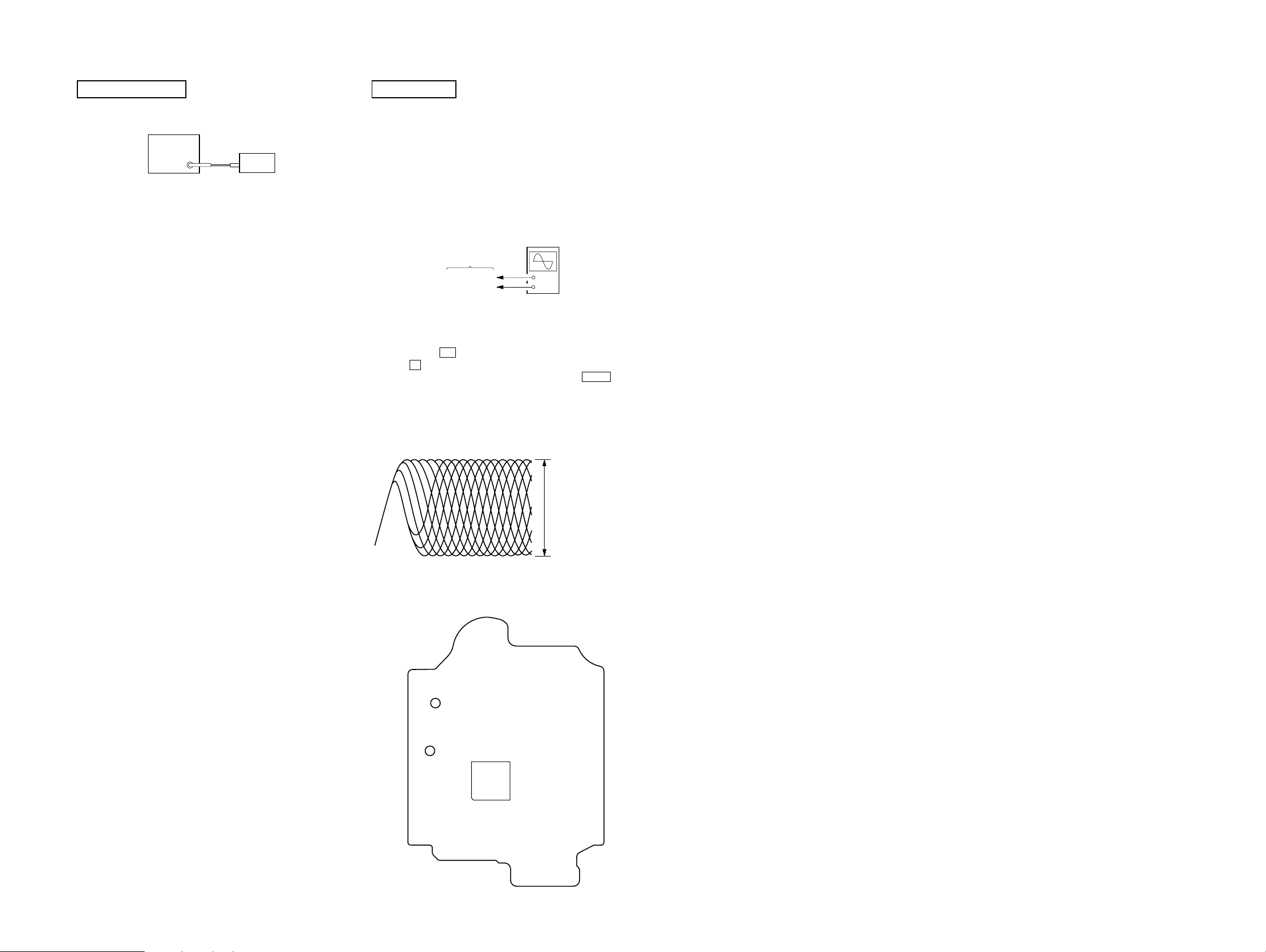
FM TUNE LEVEL CHECK
signal
generator
set
Procedure:
1. Turn on the set.
2. Input the following signal from signal generator to FM antenna
input directly.
Carrier frequency: A = 87.5 MHz, B = 98 MHz, C = 108 MHz
Deviation : 75 kHz
Modulation : 1 kHz
ANT input : 35 dBu (EMF)
Note: Use 75 ohm coaxial cable to connect signal generator and the set.
You cannot use video cable for checking.
Use signal generator whose output impedance is 75 ohm.
3. Set to FM tuner function and tune A, B and C signals.
4. Confirm “TUNED” is lit on the display for A, B and C signals.
When the selected station signal is received in good condition,
“TUNED” is displayed.
CD SECTION
Note:
1. CD Block is basically constructed to operate without adjustment.
2. Use YEDS-18 disc (3-702-101-01) unless otherwise indicated.
3. Use an oscilloscope with more than 10 MΩ impedance.
4. Clean the object lens by an applicator with neutral detergent when the
signal level is low than specified value with the following checks.
5. Check the focus bias check when optical pick-up block is replaced.
FOCUS BIAS CHECK
oscilloscop
(DC range)
CD board
TP121 (RFI)
TP124 (VC)
Procedure :
1. Connect oscilloscope to TP121 (RFI) and TP124 (VC) on the
CD board.
2. Press the I/1 button to turn the power on, and press
the Z button to open the disc tray.
3. Set disc (YEDS-18) on the tray and press the CD u button
to playback.
4. Confirm that oscilloscope waveform is as shown in the f igure
below. (eye pattern)
A good eye pattern means that the diamond shape (◊) in the
center of the waveform can be clearly distinguished.
+
–
Checking Location:
– CD Board (Conductor Side) –
TP124
(VC)
TP121
(RFI)
VOLT/DIV: 200 m
TIME/DIV: 500 ns
level:
0.9 ± 0.4 Vp-p
IC101
HCD-HX3/HX5/HX7
1717
HCD-HX3/HX5/HX7
SYSTEM CONTROLLER
IC301 (1/5)
CD-MP3 PROCESSOR
IC101
MUTE
2-AXIS
DEVICE
(TRACKING)(FOCUS)
95
89
A
AVDD
+3.3V
DETECTOR
FNi1 (A)
RFo
97 FPi1 (B)
88
2
AGCi
3RFRP RFZI
76TEi TEZi
83RFEQo 81 RFi
82 RFRPi
30LO
27RO
65AIN (PI4)
66BCKi (PI5)
BCK
A-IN
BUS1
BUS0
BUS2
BUS3
BUCK
67LRCKi (PI6)
LRCK
51PIO3
GATE
46AoUT3 (PO4)
ST-REQ
38BUS0
R-CH
94 FNi2 (C)
96 FPi2 (D)
100 TNi (E)
98 TPi (F)
91 LDo 92MDi
2 VO1+
1 VO1–
13 DMo
AUTOMATIC
POWER CONTROL
Q301
LD
PD
LASER DIODE
OPTICAL PICK-UP
BLOCK
(KSM-213DCP)
B
C
D
E
F
12 FMo
10 TRo
9FOo
20 IO0 (/HSO)
I-V AMP
M401
(SPINDLE)
M402
(SLED)
12 VO2–
11 VO2+
18 VO3+
17 VO3–
26 VO4+
27
7
IN4’
24
IN3’
20
IN2’
9
IN1
3
BIAS
23
84 VRo
VO4–
M
M
FOCUS/TRACKING COIL DRIVE,
SLED/SPINDLE MOTOR DRIVE
IC401
S201
(LIMIT)
DVDD
+3.3V
24
XO
23
XI
X102
16.9344MHz
22 CD DRIVE MUTE
LOADING
MOTOR DRIVE
IC320
CDM LOAD IN
49
CDM LOAD OUT
CDM OPEN SW
CDM CLOSE SW
48
50
51
M
A
CD-L
B
A-IN, BCK, LRCK,
GATE, ST-REQ
C
BUS0 – BUS3,
BUCK, CCE, REQ
: CD PLAY
SIGNAL PATH
R-ch is omitted due to same as L-ch.
: USB
VCC
A
B
C
D
E
F
LD
PD
SP+
VC
SP–
SL+
SL–
T+
T–
F+
F–
1 2 3 CD BUS0
13
39BUS1 4 3 2 CD BUS1
5
40BUS2 (SO) 8 9 1 CD BUS2
23 CD CLK
6
41BUS3 (SI) 11 10 100 CD BUS3
12
DATA BUS SWITCH
IC311
1 2
13
4 3
5
8 9
6
11 10
12
DATA BUS SWITCH
IC312
SIGNAL SELECTOR
IC313
A/B
Q321
42BUCK (CLK) 4
2
3
CCE
24 CD CCE
43XCCE
54SBSY
48PIO0
7
26 MP3 IREQ
6DEC BUS SEL1
19 SBSY
37XRST
25 CD XRST
5
REQ
6
12
14
13
9
10
11
1
S001
DISC TRAY
OPEN/CLOSE DETECT
OPEN
CLOSE
M001
(LOADING)
(HX7)
(HX7)
(HX3/HX5)
(HX3/HX5)
(HX3/HX5)
6-1. Block Diagram – CD SERVO Section –
SECTION 6
DIAGRAMS
(Page 20)
(Page 19)
(Page 19)
HCD-HX3/HX5/HX7
1818
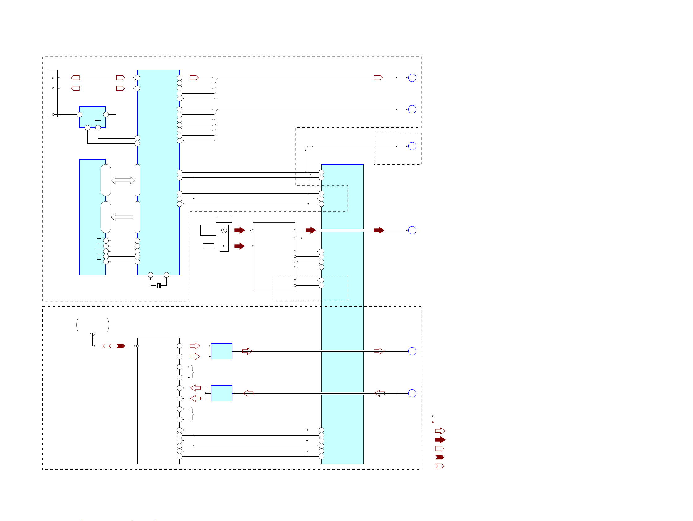
6-2. Block Diagram – TUNER/USB/BLUETOOTH Section –
HCD-HX3/HX5/HX7
CN902
(USB)
3
2
1
D+
D–
VBUS
VBUS POWER
ON/OFF SWITCH
IC915
5
EN
FLG
1
S-RAM
IC921
4OUT
IN
3
I/O0 – I/O15
7 – 10, 13 – 16,
A0 – A15
44 – 42, 27 – 24,
CE 6
OE 41
WE 17
LB
39
UB 40
VBUS
+5V
29 – 32, 35 – 38
21 – 18, 5 – 1
USB CONTROLLER
79 D+
80 D–
77 USBOC
78 USBPON
D0 – D15
18 – 25, 28 – 35
A1 – A16
37 – 43, 46 – 54
70 CS2
64
RD
65 WR
66 SRLLB
67 SRLUB
X1
75
IC901
X901
9MHz
(HX3/HX5)
A-IN, BCK, LRCK,
93DATA
92BCK
71LRCK
94GATE
97ST-REQ
55BUS0
56BUS1
57BUS2
58BUS3
59/BUCK
60/CCE
96REQ
88RXD1
X2
73
A-IN
BCK
LRCK
GATE
ST-REQ
BUS0
BUS1
BUS2
BUS3
BUCK
CCE
REQ
FM75Ω
COAXIAL
AM
ANTENNA
TUNER (FM/AM)
FM ANT
AM ANT
L OUT
R OUT
DO/STEREO
ST DIN
ST CLK
ST CE
RDS DATA
RDS CLK
(HX3: AEP/HX5: AEP,UK)
R-CH
SC_D_IN
SC_D_OUT
35 USB TXD/SAT TXD
36 USB RXD/SAT RXD87TXD1
38 USB_RTS2DI
37 USB_CTS84DO
27 USB RESET1/RESET
88 ST DATA IN/STEREO
90 ST DATA OUT
89 ST CLK
87 ST CE
86 RDS DATA
18 RDS INT
SYSTEM CONTROLLER
IC301 (2/5)
GATE, ST-REQ
BUS0 – BUS3,
BUCK, CCE, REQ
SC_D_IN,
SC_D_OUT
TUNER-L
B
(Page 18)
C
(Page 18)
D
(Page 20)
(HX7)
E
(Page 20)
ANT901
PATTERN
ANTENNA
(FOR BLUETOOTH)
IC904
BLUETOOTH MODULE
10A_OUT_P_L
9A_OUT_N_L
8A_OUT_P_R
R-CH
7A_OUT_N_R
5A_IN_P_L
4A_IN_N_L
3A_IN_P_R
R-CH
2A_IN_N_R
40UART_RXD
41UART_TXD
38UART_CTS
39UART_RTS
46RESET
MIX AMP
IC902
LINE AMP
IC901
31 BT_DOUT/DAB TXD
32 BT_DIN/DAB RXD
34 BT_RTS
61 BT_CTS
60 BT_AV_ROLE12PIO_00
63 BT RESET
BT-L
BT OUT-L
F
(Page 20)
G
(Page 20)
(HX5/HX7)
R-ch is omitted due to same as L-ch.
SIGNAL PATH
: AUDIO
: TUNER (FM/AM)
: USB
: BLUETOOTH IN
: BLUETOOTH OUT
HCD-HX3/HX5/HX7
1919
HCD-HX3/HX5/HX7
6-3. Block Diagram – MAIN Section –
A
(Page 18)
F
(Page 19)
(HX5/HX7)
E
(Page 19)
(HX7)
D
(Page 19)
J981
AUDIO IN
CD-L
BT-L
TUNER-L
SC_D_IN,
SC_D_OUT
SC_D_IN
SC_D_OUT
J001
XM
3
2
1
R-CH
D+
D–
VCC
DATA BUS SWITCH
IC318
11 10
1 2
8 9
4 3
R-ch is omitted due to same as L-ch.
SIGNAL PATH
: AUDIO
: TUNER (FM/AM)
: CD PLAY
: XM
: SIRIUS
: AUDIO IN
(HX3/HX5)
BT OUT-L
INPUT SELECTOR, ELECTRICAL VOLUME,
SURROUND/TONE CONTROL
IC304
XM RECEIVER
IC001
18 COMM_RX_P
19 COMM_RX_N
23 COMM_TX_P
22 COMM_TX_N
OSC_IN
OSC_OUT
5
2628
X001
45.158MHz
12
13
6
5
Q320
SC_TX_OUT
SC_RX_IN
11
3
RST#
37I2S_DA
39I2S_CLK
41I2S_LRCLK
43I2S_OCLK
XM
+3.3V
D216
B+ SWITCH
Q001, 003
B+ SWITCH
Q314, 315
D/A CONVERTER
IC041
3 SDTI
2 BICK
4 LRCK
1 MCLK
XM
+5.4V
+4V
AOUTR
PDN
R-CH
LINE AMP
IC051
11AOUTL
10
5
INPUT SELECTOR
IC303
X0
12
X2
15
X3
11
10A9
Q309
Q308
INL1
4
INL2
5
INL4
X
13
B
INH
6
Q311
7
6
8
9
INL3
IGOUTL
VOLINL
22
DATA21CLK
LOUT
27
MUTING
IC315
MUTING
CONTROL SWITCH
Q303, 304
(HX5/HX7)
OUTPUT SELECTOR
X
13
Q328
R-CH
IC310
A
10
X1
14
X0
12
(HX3)
HEADPHONE
AMP
IC317
CONTROL SWITCH
MUTING
IC316
MUTING
Q306, 307
R-CH
R-CH
(Page 19)
(HX5/HX7)
J982
PHONES
L-CH
(Page 21)
G
H
J301
SIRIUS
HCD-HX3/HX5/HX7
3 SSP_D_OUT
6 SSP_D_IN
8 L_OUT
5 R_OUT
2 PWR ENABLE
R-CH
LEVEL SHIFT
IC321
B+ SWITCH
Q316, 317
94
SR_POWER
XM
+5.4V
93
SAT SEL
91
XM RESET
69
92
XM_PWR_3.3V/5V
AUDIO IN DET
2020
58
SEL A57SEL B
SYSTEM CONTROLLER
59
SEL INH
IC301 (3/5)
55
56
AMP DATA
AMP CLOCK
54
TA LINE-MUTE
53
BT AUD OUT MUTE
(HX5/HX7)
52
HP MUTE
68
HP DET
6-4. Block Diagram – AMP Section –
HCD-HX3/HX5/HX7
L-CH
H
(Page 20)
49.152MHz
X702
A/D CONVERTER
IC701 (HX3/HX7)
IC701 (HX5)
1
15 SCKI
DOUT
LIN
LRCK
CLOCK SHIFT
IC703 (HX3/HX7)
IC703 (HX5)
CLOCK BUFFER
IC709 (HX3/HX7)
IC709 (HX5)
SYSTEM CONTROLLER
IC301 (4/5)
S-MASTER DATA
S-MASTER SHIFT
S-MASTER LATCH
S-MASTER PG MUTE
S-MASTER SOFT MUTE
S-MASTER NSP MUTE
S-MASTER INIT
S-MASTER RST
S-MASTER SD
STREAM PROCESSOR
IC705 (HX3/HX7)
IC705 (HX5)
12
11
12
43
42
33
47
7
40
39
45
44
31 DATA
30 BCKBCK
29 LRCK
36 XFSIIN
48 XFSOIN
21 SCDT
22 SCSHIFT
23 SCLATCH
20 PGMUTE
19 SOFTMUTE
18 NSPMUTE
27 INIT
OUTL1
OUTL2
OUTR1
OUTR2
11
9
6
4
(HX3/HX7)
DIGITAL POWER AMP
IC707
4 PWM_A
6 PWM_B
14 PWM_C
16
PWM_D
/RST_AB
15
5
DIGITAL POWER AMP
IC707
2 BP
17 AP
/RST
4
DIGITAL POWER AMP
IC708
OUT_A
OUT_B
OUT_C
OUT_D
/SD
/RST_CD
3
OUT_B
OUT_B
OUT_A
OUT_A
/SD
3
J860
33
30
25
22
29
30
25
26
L.P.F.
L.P.F.
L.P.F.
L.P.F.
PROTECT
DETECT
Q701
OVER LOAD
DETECT
Q702, 703
OVER LOAD
DETECT
Q752, 753
+
–
L
SPEAKER
R
+
–
2 DP
17 CP
4
/RST
(HX5)
OUT_D
OUT_D
OUT_C
OUT_C
/SD
3
29
30
25
26
R-ch is omitted due to same as L-ch.
SIGNAL PATH
: AUDIO
HCD-HX3/HX5/HX7
2121
HCD-HX3/HX5/HX7
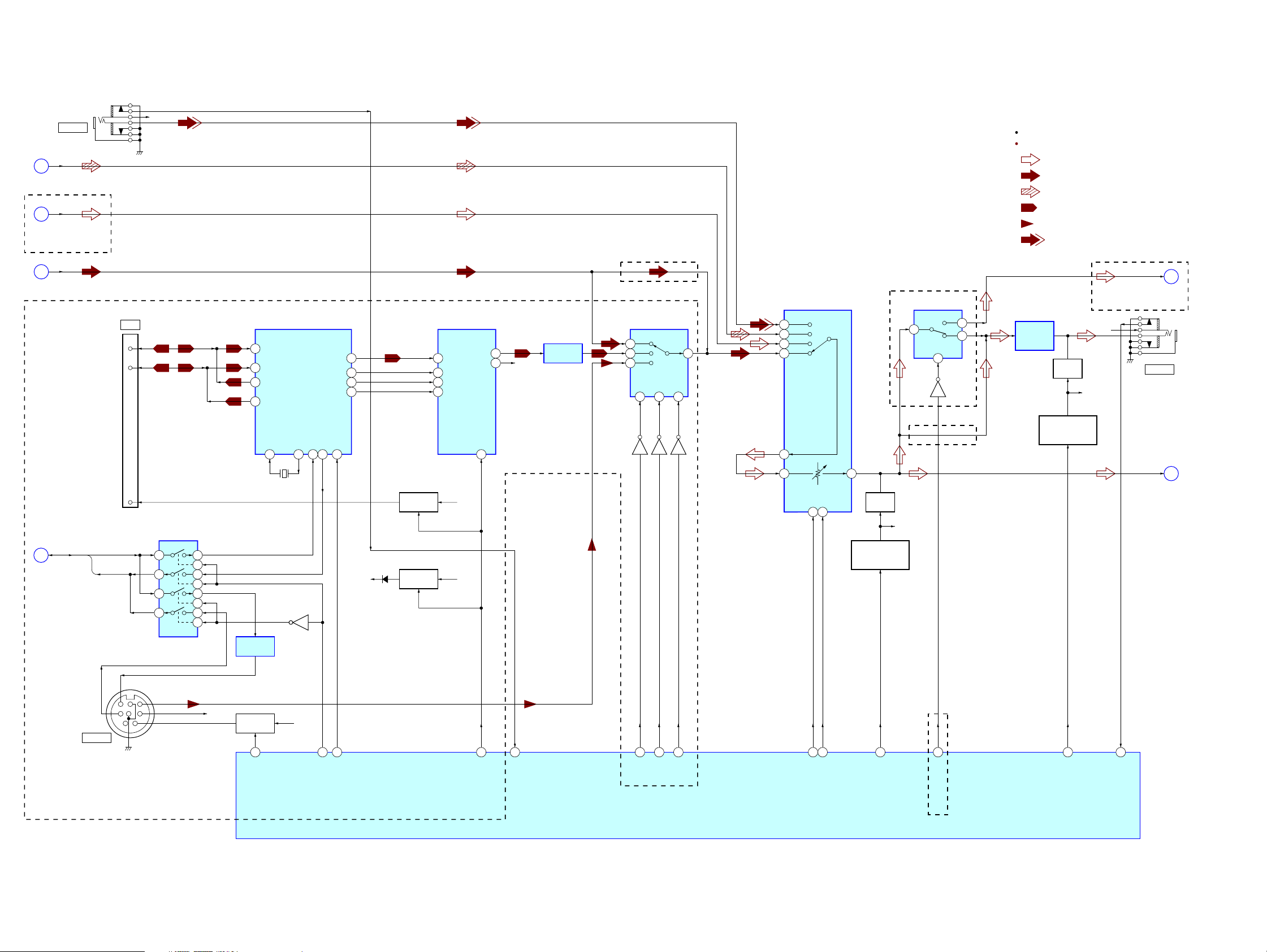
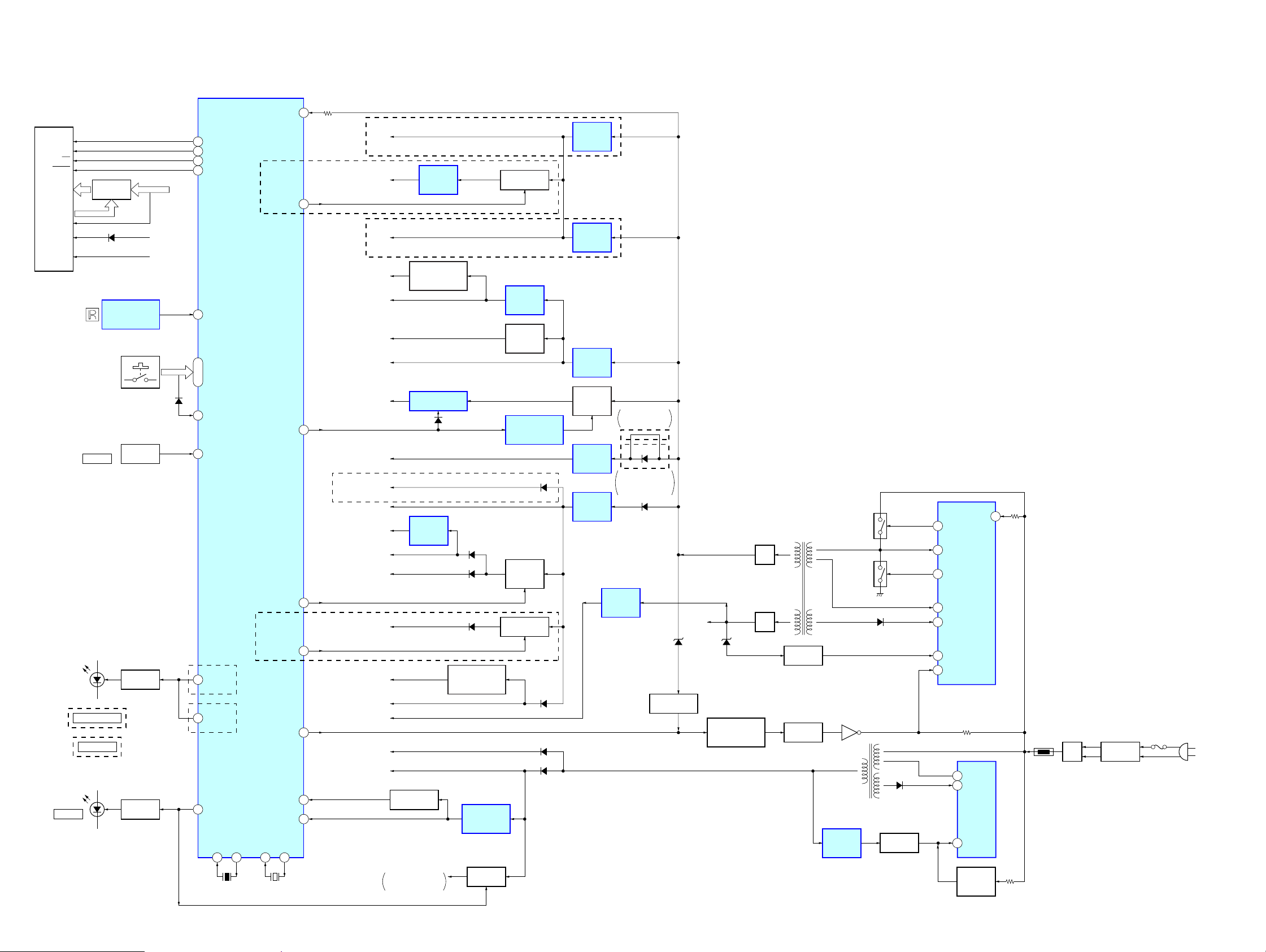
6-5. Block Diagram – PANEL/POWER SUPPLY Section –
SYSTEM CONTROLLER
IC301 (5/5)
FL901
FLUORESCENT
INDICATOR TUBE
DA
CP
CS
RESET
1G, 12G
Q1, Q12
VH
F+
VDD
D951
STANDBY
GRID DRIVE
Q901, 902
D909
REMOTE CONTROL
S951 – 954,
S961 – 963,
S965 – 968,
S970 – 976
RV952
VOLUME
D952
USB MEMORY
(HX3)
BLUETOOTH
(HX5/HX7)
RECEIVER
IC951
ROTARY
ENCODER
LED DRIVE
Q953
LED DRIVE
Q951
+7V
EVER +3.3V
D218, 219
VH B+
73
FL SD
FL SCLK
71
FL CS
72
FL RESET
75
4 SIRCS
KEY0 – KEY2
83 – 81
74 KEY WAKE UP
84 VOLUME JOG
(HX3)
76 USB LED
77 BT LED
(HX5/HX7)
78 STBY LED
XIN
13
15
X302
5MHz
(HX5/HX7)
XOUT
10
32.768kHz
XCIN
X301
85AC DET
65BT POWER
70FL POWER ON
21CD ON
28USB POWER
80STBY RELAY
12RESET
20AC CUT
XCOUT
11
VBUS
+5V
(HX3/HX5)
+3.3V
XM
+5.4V
(HX7)
+3.3V
(FOR ADC )
+9V
(FOR HP AMP)
VH B+
+3.3V
(FOR IC311 –313)
+1.5V
DVDD
+3.3V
AVDD
+3.3V
USB
+3.3V
+1.8V
AMP
+3.3V
+12V
µ-COM
+3.3V
EVER
+3.3V
BT
+5V
+9V
+7V
+4V
RESET SWITCH
Q301
+3.3V
FOR
ROTARY ENCODER
+3.3V
REGULATOR
IC903
+3.3V REGULATOR
IC702 (HX3/HX7)
IC702 (HX5)
B+ SWITCH
IC901-2, Q904, 908
D903
+1.5V
REGULATOR
IC201
+1.8V REGULATOR
D211
D212
D213
IC704 (HX3/HX7)
IC704 (HX5)
RESET SIGNAL
GENERATOR
IC302
B+ SWITCH
Q952
B+ SWITCH
Q302, 323, 324
+5V
REGULATOR
IC308
RIPPLE
FILTER
Q305
POWER CONTROL
SWITCH
IC901-1, Q903, 905
D210
(HX3/HX5)
B+ SWITCH
Q312, 313,
325, 326
B+ SWITCH
Q327, 329, 330
(HX3/HX5)
D203
D221
D220
SWITCHING
REGULATOR
IC319
+5.4V
REGULATOR
IC309
+9V
REGULATOR
IC305
DC/DC
CONVERTER
Q906, 907
+7V
REGULATOR
IC306
+4V
REGULATOR
IC307
HX3: AEP/HX5:
AEP, UK/HX7
HX3: Canadian/
HX5: Canadian,
Australian, Korean
+12V
REGULATOR
IC12
D209
D205 – 207
D652 D33
DC DETECT
Q651, 652
+27V
POWER ON/OFF
CONTROL SWITCH
Q650
RECT
D31
RECT
D32
T31
MAIN POWER
TRANSFORMER
ISOLATOR
PH11
ISOLATOR
PH602
SWITCHING
SWITCHING
Q601
TRANSFORMER
SHUNT
REGULATOR
IC650
Q12
Q11
T603
SUB POWER
D14
ISOLATOR
D603
PH601
16 VG (H)
15 VS
12 VG (L)
9 OCP
8 VC1
2 F/B
1 VSENSE
POWER CONTROL
IC11
5 DRAIN
4
VCC
POWER
CONTROL
2 FB
FEED BACK
SWITCH
IC601
Q615
18
VD
(AC IN)
TH1
RECT
D1
LINE FILTER
T1
F1
HCD-HX3/HX5/HX7
2222
• Circuit Boards Location• Note For Printed Wiring Boards and Schematic Diagrams
d
• Circuit Boards Location
HCD-HX3/HX5/HX7
Note on Printed Wiring Board:
• X : parts extracted from the component side.
• Y : parts extracted from the conductor side.
• f : internal component.
• : Pattern from the side which enables seeing.
(The other layers' patterns are not indicated.)
Caution:
Pattern face side: Parts on the pattern face side seen from
(Conductor Side) the pattern face are indicated.
Parts face side: Parts on the parts face side seen from
(Component Side) the parts face are indicated.
Caution:
Pattern face side: Parts on the pattern face side seen from
(Side B) the pattern face are indicated.
Parts face side: Parts on the parts face side seen from
(Side A) the parts face are indicated.
• Indication of transistor
C
Q
B
E
B
These are omitted.
Q
CE
These are omitted.
Note on Schematic Diagram:
• All capacitors are in µF unless otherwise noted. (p: pF)
50 WV or less are not indicated except for electrolytics
and tantalums.
• All resistors are in Ω and 1/
specified.
• f : internal component.
• 2 : nonflammable resistor.
• C : panel designation.
Note:
The components identified by mark 0 or dotted
line with mark 0 are critical for safety.
Replace only with part
number specified.
• A : B+ Line.
• Voltages and waveforms are dc with respect to ground
under no-signal (detuned) conditions.
– CD Board –
no mark : CD PLAY
[]: USB
– USB and USB POWER Boards –
no mark : USB
– BT Board –
no mark : BLUETOOTH
– XM and XM REGULATOR Boards –
no mark : XM
– Other Boards –
no mark : TUNER (FM/AM)
(): CD PLAY
[]: USB
{ }: BLUETOOTH
〈〈 〉〉 : XM
<>: SIRIUS
∗ : Impossible to measure
• Voltages are taken with a VOM (Input impedance 10 MΩ).
Voltage var iations may be noted due to normal production tolerances.
• Waveforms are taken with a oscilloscope.
Voltage var iations may be noted due to normal production tolerances.
• Circled numbers refer to waveforms.
• Signal path.
F : AUDIO
f : TUNER (FM/AM)
J : CD PLAY
d : USB
E : BLUETOOTH IN
j : BLUETOOTH OUT
: XM
O : SIRIUS
h : AUDIO IN
• Abbreviation
AUS: Australian model
CND : Canadian model
KR : Korean model
4
W or less unless otherwise
Note:
Les composants identifiés par
une marque 0 sont critiques
pour la sécurité.
Ne les remplacer que par une
pièce portant le numéro
spécifié.
TOP PANEL (FUNCTION) board
FRONT PANEL board
CD board
MOTOR board
XM REGULATOR board
(HX7)
USB board
(HX3/HX5)
XM board
(HX7)
TOP PANEL (PLAY) board
USB POWER board
(HX3/HX5)
H/P SUPPORT boardHEADPHONE board
TUNER (FM/AM) MAIN board
BT board
(HX5/HX7)
ANT board
(HX5/HX7)
SPEAKER boar
SUB POWER board
SWITCHING POWER board
AMP board
HCD-HX3/HX5/HX7
2323
HCD-HX3/HX5/HX7
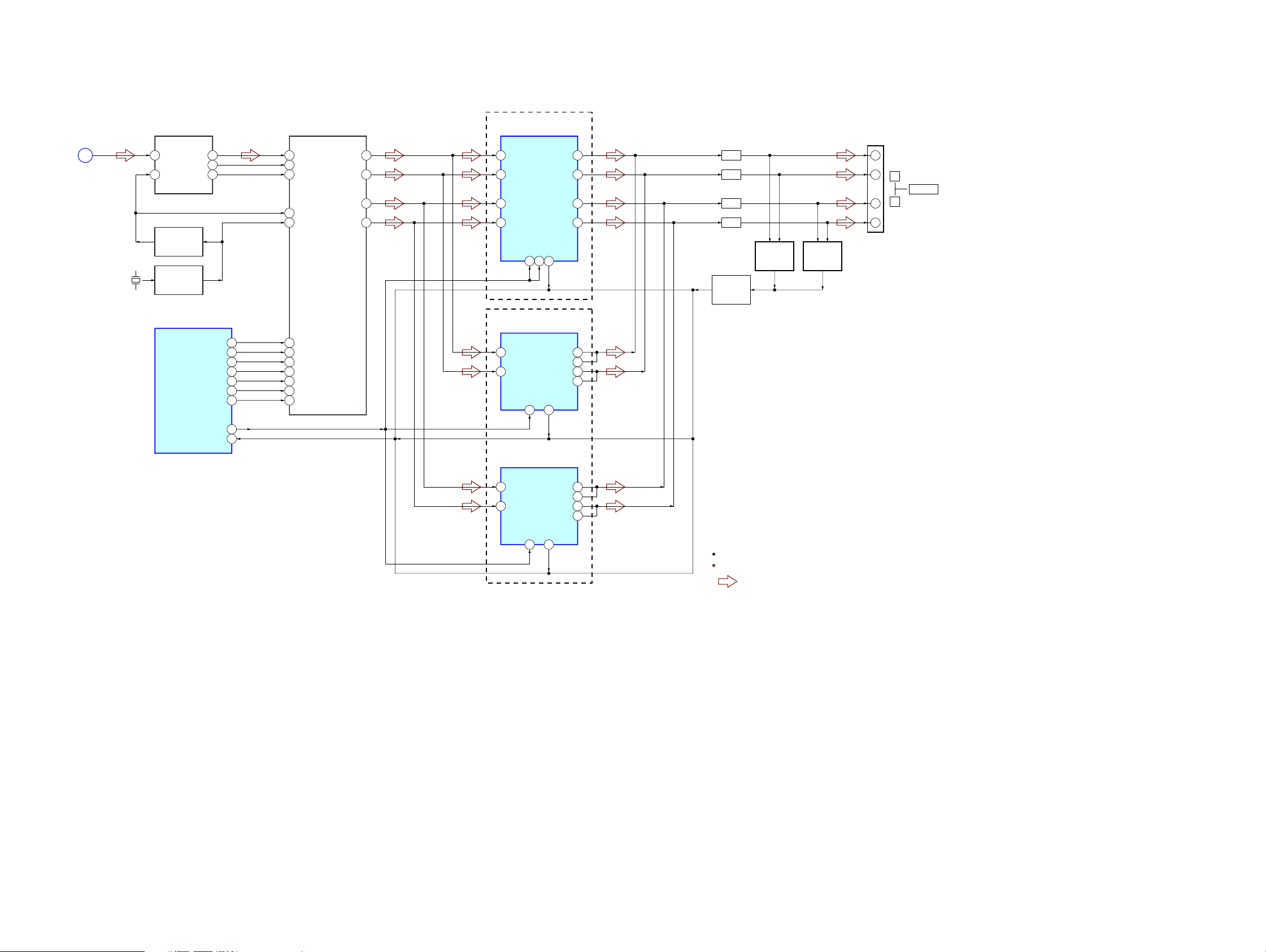
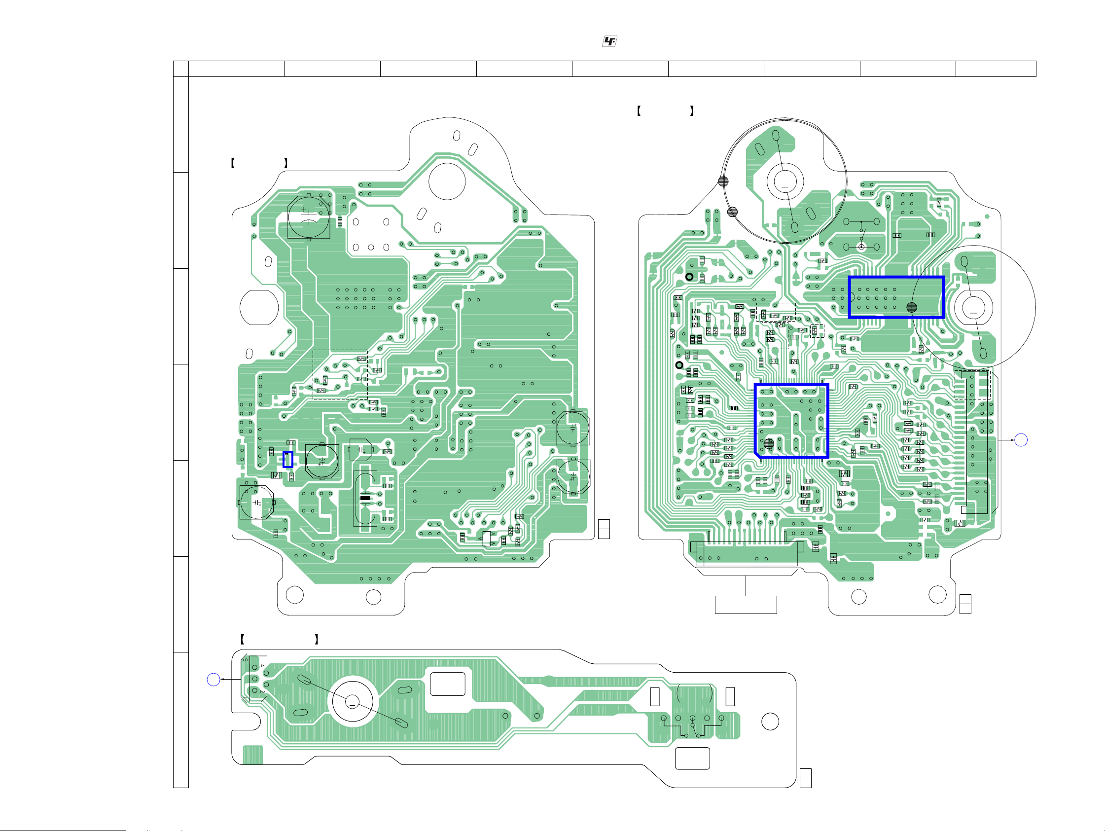
6-6. PRINTED WIRING BOARDS – CD Section –
1
2 3 4 567 8 9
A
CD BOARD
B
(COMPONENT SIDE)
C401
C405
C
(HX3/HX5)
R211
R215
D
C207
IC201
5
C206
314
R201
E
C202
C204
C201
C205
R216
X102
R213
R214
C115
R212
R112
R111
C133
R155
C130
C128
• See page 23 for Circuit Boards Location. :Uses unleaded solder.
C309
Q301
CD BOARD
TP121
(RFI)
C106
C306
R303
R302
E
C307
R301
R304
1-872-135-
11
(11)
(CONDUCTOR SIDE)
TP124
(VC)
C122
R140
C123
R142
R135
R143
R151
C138
C137
C140
C139
C141
C142
R144
C146
C143
C144
C148
C149
C147
R146
R148
C150
C125
C124
R136
C145
R134
C105
C104
C118
R139
R130
C100
R145
R147
R149
R150
R129
76
100
C117
CN301
C136
R128
R123
C107
1
C120
R122
R126
R125
C112
C119
M
(HX3/HX5)
R124
R127
(HX7)
IC101
C101
161
C153
R114
C102
C103
C126
C127
(SPINDLE)
R118
C113
M401
(HX7)
R101
C303
R402
5175
25
R120
R102
S201
(LIMIT)
28 22 21 15
17 814
R415
R414
C108
R113
50
C110
C109
R153
R154
C116
C132
R105
C301
C302
26
R104
R106
R110
C404
IC401
R210
R209
R218
R219
R220
R221
R222
R223
R157
R156
R108
R405
C403
M402
(SLED)
M
R408
(HX3/HX5)
1
R208
R207
R206
R205
R204
R203
C151
C152
CN201 (HX7)
25
R202
CN203 (HX3/HX5)
(Page 32)
A
MAIN
BOARD
CN308
HCD-HX3/HX5/HX7
F
G
B
MAIN BOARD
CN320
(Page 32)
MOTOR BOARD
CN001
M
M001
(LOADING)
11
(11)
S001
DISC TRAY
OPEN/CLOSE
DETECT
OPEN T CLOSE
OPTICAL PICK-UP BLOCK
(KSM-213DCP)
1-866-548-
1-872-135-
21
(21)
2424
HCD-HX3/HX5/HX7
6-7. SCHEMATIC DIAGRAM – CD Section –
CN301
16P
OPTICAL
PICK-UP
BLOCK
(KSM-213DCP)
M401
(SPINDLE)
M
M402
(SLED)
M
SP-
SP+
SL+
SL-
• See page 41 for Waveforms. • See page 46 for IC Block Diagrams. • See page 53 for IC Pin Function Description.
R127
C107
0.1
Q301
2SA2119K
AUTOMATIC POWER
C301
0.1
C405
0.1
CONTROL
C306
R303
100
2.2
C303C302
1010
C404
0.1
10V
R304
2.2
C309
0.001
C403
0.1
R301
100k
C307
1
R302
0
R143
47k
C137
0.01
1
C100
0.1
C139
C106
100
10V
C105
0.1
C144
0.1
C148
47p
C149
C104
0.1
C140
C141
C142
TP124 (VC)
R144
C143
C146
C145
R145
R146
R147
R148
R149
C150
R405
10k
R402
2.2k
0.01
TP121 (RFI)
R142 R139
22k 47k
470p
C138
0.01
0.0022
0.1
22k
0.01
470p
0.01
0.1
C147
22p
0
0
0
0
0
0.001
R150
0
C136
47p
R129
1k
R134
R140
0
1M
R136 R135
22k 470k
R130
4.7k
C118
0.01
R125
470k
C112 C108
0.1 0.1
R128
C117
0.022
C119
0.022
C120
0.01
R124
0
0
0
00
R126 R123
R122
0
R118
100k
IC101
CD-MP3 PROCESSOR
IC101
TC94A70FG-006 (HX7)
TC94A70FG-007 (S, D) (HX3/HX5)
0
R151
0.1
C102
0.0047
C123
470p
C124
C122
470p
0.0047
C125
C101
0.1
(HX3/HX5)(HX7)
C153
R120
(HX7)
R114
0.1
0
10k
10k
R113
0.1
C133
R112
100
100
R111
R110
10k
0.1
C110
R153
1M
R154
C115
R155
47
22
6.3V
0.1
C116
1M
R108
0
2
1k
1M
220
R101
0.0022
C127
0.1
C126
0.1
C113
C103
0.1
R105
R106
X102
16.9344MHz
5p
C128
R102
10k
5p
C130
C132
0.1
R104
0
CN201
21P (HX7)
CN203
(HX3/HX5)
R216 100
R215 100
R214 100
R213 100
R212
100
R210
100
R209
100
R218
100k
R219
100k
R220
100k
R221
100k
R222
100k
R223
100k
R208
100
R207
100
R206
100
R205
100
R204
100
R203
100
R211
25P (HX3/HX5)
100
A
MAIN
BOARD(3/3)
CN308
(Page 35)
IC B/D
C207
1
R157
100
R156
100
C205
C201
0.1
100
TK63115SCL-G@GT (HX7)
10V
100
10V
XC6215B152MR (HX3/HX5)
IC201
+1.5V REGULATOR
C204
0.1
C109
0.1
C202
IC201
C206
1
C151
470p
470p
C152
R201
0
R202
0
S201
(LIMIT)
HCD-HX3/HX5/HX7
IC401
FOCUS/TRACKING COIL DRIVE,
SLED/SPINDLE MOTOR DRIVE
IC401
BA5826SFP-E2
SP-
SP+
R414
4.7k
IC B/D
SL+
SL-
R408
2.2k
C401
R415
220
47k
10V
2525
HCD-HX3/HX5/HX7
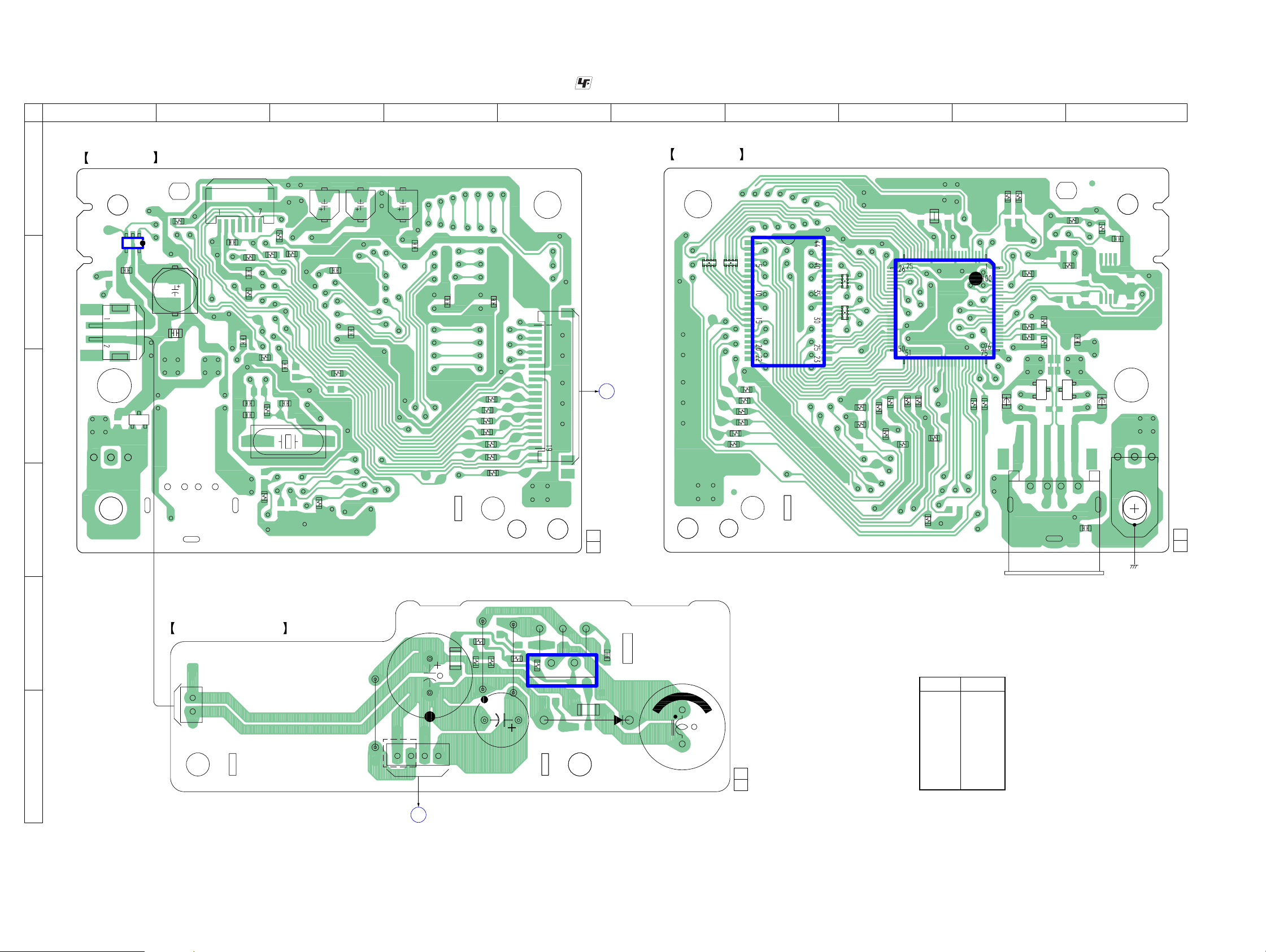
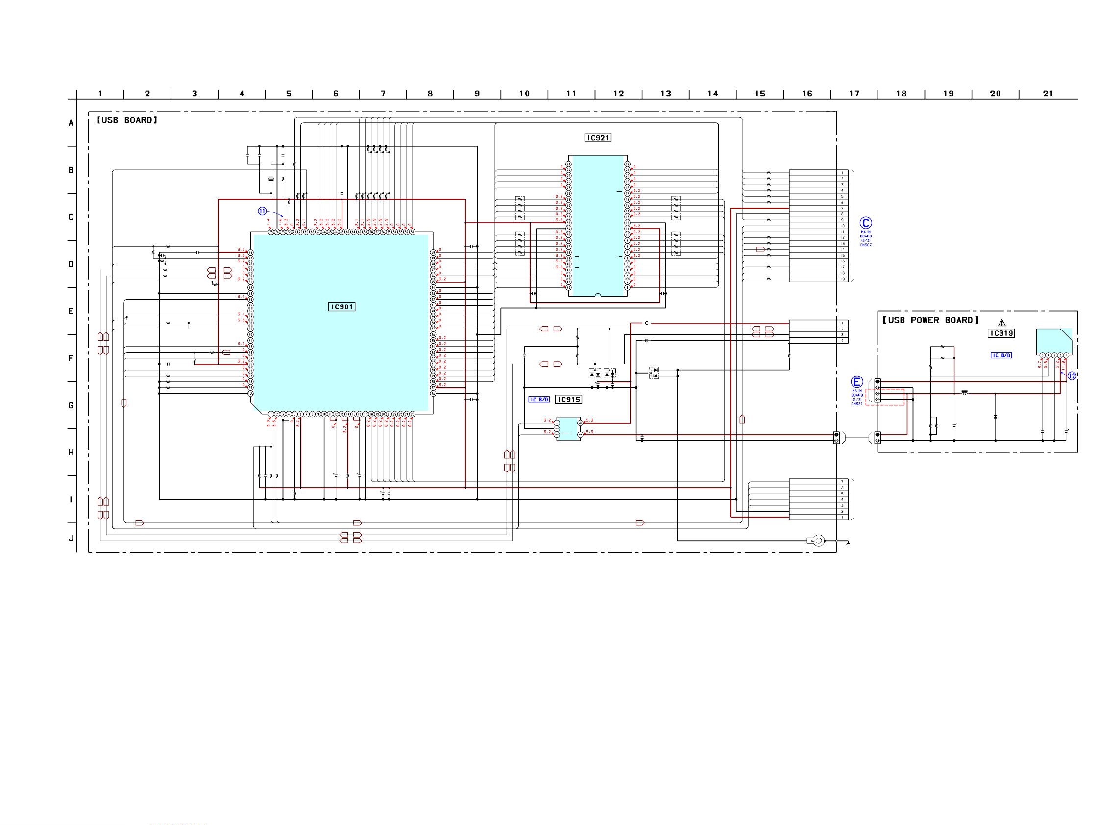
6-8. PRINTED WIRING BOARDS – USB Section (HX3/HX5) –
1 2 3 4 5 6 7 8 9 10
USB BOARD
A
31
IC915
45
B
CN908
C
D
(COMPONENT SIDE)
R928
C916
C917
C918
A/K
D905
K
A
C901
C915
R934
C910
C912
(NC)
CN904
C913
X901
R938
R922
R919
R913
R901
R937
C902
R983
C908
C909
R915
• See page 23 for Circuit Boards Location. :Uses unleaded solder.
C903
C907
C906
R981
C904
C905
C922
R978
R979
R932
R982
R984
R977
R976
C921
CN905
1-872-405-
11
(11)
C
MAIN BOARD
CN307
(Page 32)
USB BOARD
RB922 RB921
R975
R974
R973
R972
R971
R970
(CONDUCTOR SIDE)
IC921
RB924
RB923
R941
R902
R942
R943
R904
R903
JR902
R944
R907
IC901
R905
R906
R916
R950
R917
FB901
R933
R924
R923
R948
A
K
R946
A/K
D901
CN902
(USB)
R921
R926
R925
A/K
C930
C920
D902
R920
C914
K
FB902
A
EP901
14
11
1-872-405-
(11)
(CHASSIS)
E
F
USB POWER BOARD
1
CN324
2
JW556
(HX5)
CN322
E
C325
MAIN BOARD
CN321
14
JR360
R315
JW555
R314
R307
R317
C324
15
R409
JW554
IC319
42
JR361
D208
C358
L101
1-873-248-
11
(11)
• Semiconductor
Location
Ref. No. Location
D208 F-6
D901 C-9
D902 C-10
D905 C-1
IC319 E-5
IC901 B-8
IC915 B-1
IC921 B-7
(Page 32)
HCD-HX3/HX5/HX7
2626
HCD-HX3/HX5/HX7
6-9. SCHEMATIC DIAGRAM – USB Section (HX3/HX5) –
LRCK
DVCC
USBOC
USBPON
D+
D-
AM0
NO USE
DVSS
DO
DATA
CLOCK
TXD1
RXD1
NO USE
SDA
SCL
BCK
DATA
GATE
DVCC
REQ
ST-REQ
G-1
G-2
DVSS
C909
22p
R916
0
R919
100
X901
9MHz
R917
0
X2
X1
AM1
DVSS
/RESET
NO USE
NO USE
DI
C910C912
22p10p
BOOT
100k
FLG
EN
AMO
DO
USB-SO
TXD1
USB-SI
RXD1
BCK
A-IN
GATE
REQ
ST-REQ
R921
R920
10k
0.1
C914
100k
R922
27
R923
27
R924
R981
C915
R938
R946
R948
0.1
C913
R928
0
100
0
R933
10k
0.1
R934
100
4.7k
4.7k
LB
UB
SRAM-CS
10k
100k
R915
R913
CS2
LRCK
BOOT
SRLUB
NO USE
NO USE
NO USE
NO USE
DVCC
G-3
• See page 41 for Waveforms. • See page 46 for IC Block Diagrams. • See page 53 for IC Pin Function Description.
RD
WR
RD
WR
SRLLB
USB CONTROLLER
IC901
TMP92CD28FG-2CB2
RVOUT1
DVCC
DVSS
CCE
BUS3
BUCK
100k
R944
4.7k
4.7k
0.1
C908
4.7k
R907
R906
R905
/CCE
DVSS
DVCC
RVIN
BUS3
/BUCK
NO USE
RVOUT2
RVIN
D0
DVSS
DVCC
A14
A16
A15
A13
BUS1
BUS0
BUS2
S-RAM
IC921
R926
R925C920
IC915
R5523N001BTR-F
EN
GND
FLG
IS61LV6416-10T
NC
A6
A5
A4
A3
NC
I/O8
I/O9
I/O10
I/O11
VDD
GND
I/O12
I/O13
I/O14
I/O15
UB
OE
A2
A1
A0
15k
15k0.1
D901
MC2837
OUT
IN
NC
A7
A8
A9
A10
WE
I/O7
I/O6
I/O5
I/O4
GND
VDD
I/O3
I/O2
I/O1
I/O0
CELB
A11
A12
A13
A14
A15
D902
MC2837
C918C917
10220
6.3V
C921
0.1
FB902
FB901
D905
MC2837
C916
0.1
A8
A9
A10
A11
WR
D7
D6
D5
47
RB922
D4
D3
D2
D1
47
RB921
D0
SRAM-CS
A12
A13
A14
A15
A16
CCE
BUCK
BUS3
BUS2
BUS1
BUS0
LRCK
USB-RST
ST-REQ
REQ
GATE
A-IN
BCK
USB-SI
USB-SO
DI
DO
100
R970
100
R971
100
R972
100
R973
100
R974
100
R975
100
R976
100
R977
100
R978
100
R979
100
R932
100
R982
100
R984
100k
100k
100k
R943
R941
R942
4.7k
4.7k
4.7k
R904
R902
R903
A14
A16
A15
A13
BUS0
BUS2
BUS1
D3
S2
D1
A12
A11
A10
A9
A8
DVCC
DVSS
A7
A6
A5
A4
A3
A2
A1
A0
D15
D14
D13
D12
D11
D10
D9
D8
DVCC
DVSS
D7
D6
D5
D4
C907
C906
A7
A6
A5
A4
RB923
47
D8
D9
D10
D11
RB924
47
D12
D13
0.1
D14
A12
D15
LB
A11
UB
A10
RD
A9
A8
A3
A2
A1
A7
A6
A5
A4
A3
A2
A1
D15
D14
D13
D12
D11
D10
D9
D8
0.1
C922
0.1
VBUS POWER ON/OFF SWITCH
EN
FLG
C930
CCE
BUCK
BUS3
BUS2
BUS1
BUS0
DVDD3.3V
DVSS
LRCK
USB-RST
ST-REQ
REQ
GATE
A-IN
BCK
USB-SI(RXD)
USB-SO(TXD)
DI(CTS)
DO(RTS)
VBUS
D-
D+
GND
0
VBUS-5V
VBUS-GND
CN908
CN905
19P
CN902
(USB)
2P
4P
(Page 35)
(Page 34)
CN322
2P(HX3)
4P(HX5)
+11V
GND
DVDD_5V
DGND
(HX5)
CN324 R314
2P 1k
VBUS-5V
VBUS-GND
R307
100k
R317
4.7k
R315
0
R409
4.7k
SWITCHING REGULATOR
IC319
SI-8008TFE
L101
47µH
D208
C325
2200
16V
21DQ04
C358
0.1
IN
SW
SS
GND
ADJ
C324
220
25V
16V
16V
10k
0.1
100
100
R901
C901
R937
R983
R950
4.7k
USB-RST
DI
RESET
0
10
10
C903
C902
JR902
D1
D0
C904
10
16V
D7
D6
D5
D4
D3
D2
C905
0.1
BOOT
AM0
TXD1
RXD1
RESET
CN904
7P
BOOT
AM0
TXD1
RXD1
RESET
DVSS
VCC
EP901
(NC)
(CHASSIS)
HCD-HX3/HX5/HX7
2727
 Loading...