

Page 1

HCD-HPX11D
SERVICE MANUAL
Ver 1.0 2004.07
HCD-HPX11D is the amplifier, DVD player,
tape deck and tuner section in CMT-HPX11D.
DVD
Section
Tape deck Model Name Using Similar Mechanism HCD-M333
Section Tape Transport Mechanism Name CMAL1Z-236A
E Model
Australian Model
Model Name Using Similar Mechanism NEW
DVD Mechanism Type CDM82B-DVBU28
Optical Pick-up Block Name DBU-3
Amplifier section
The following measured at AC 120, 127, 220, 240 V,
50/60 Hz
DIN power output (rated): 55 + 55 W
(6 ohms at 1 kHz, DIN)
Continuous RMS power output (reference) :
70 + 70 W
(6 ohms at 1 kHz, 10%
THD)
Inputs
MD/VIDEO (phono jacks):
Sensitivity 450/250 mV,
impedance 47 kilohms
MIC (mini jack): Sensitivity 1 mV,
impedance 10 kilohms
Outputs
PHONES (stereo mini jack):
Accepts headphones with
an impedance of 8 ohms or
more.
SPEAKER: Accepts impedance of 6 to
16 ohms.
Disc player section
System Compact disc and digital
audio and video system
Laser Semiconductor laser
(DVD: λ = 645 – 660 nm,
CD: λ= 770 – 800 nm)
Emission duration:
continuous
SPECIFICATIONS
Frequency response 20 Hz – 20 kHz
Video color system format:
NTSC, PAL
Tape deck section
Recording system 4-track 2-channel, stereo
Frequency response 50 – 13,000 Hz (±3 dB),
using Sony TYPE I
cassettes
Tuner section
FM stereo, FM/AM superheterodyne tuner
FM tuner section
Tuning range 87.5 – 108.0 MHz
Antenna FM lead antenna
Antenna terminals 75 ohms unbalanced
Intermediate frequency 10.7 MHz
AM tuner section
Tuning range
Saudi Arabian models: 531 – 1,602 kHz
(with the interval set at 9
kHz)
Other models: 530 – 1,710 kHz
(with the tuning interval
set at 10 kHz)
531 – 1,602 kHz
(with the interval set at 9
kHz)
Antenna AM loop antenna, external
antenna terminal
Intermediate frequency 450 kHz
General
Power requirements
Australian model: 230 – 240 V AC, 50/60 Hz
Saudi Arabian model: 120 – 127, 220 or 230 –
240 V AC, 50/60 Hz
Adjustable with voltage
selector
Thai model: 220 V AC, 50/60 Hz
Other models: 120, 220 or 230 – 240 V
AC, 50/60 Hz
Adjustable with voltage
selector
Power consumption 140 W
Dimensions (w/h/d) Approx. 196 × 270 × 402
mm incl. projecting parts
and controls
Mass Approx. 9.7 kg
Design and specifications are subject to change
without notice.
9-877-999-01
2004G1678-1
© 2004.07
DVD DECK RECEIVER
Sony Corporation
Home Audio Company
Published by Sony Engineering Corporation
Page 2

HCD-HPX11D
Don’t throw away the battery with
general house waste, dispose of it
correctly as chemica l waste.
E
NERGY STAR
®
ENERGY STAR® is a U.S.
registered mark. As an E
®
S
TAR
partner, Sony Corporation
has determined that this product
meets the E
NERGY STAR
NERGY
®
guidelines for energy efficiency.
This system incorporates Dolby1) Digital adaptive
matrix surround decoder and DTS
2)
Digital Surround
System.
1)
Manufactured under license from Dolby
Laboratories.
“Dolby” and the double-D symbol are trademarks of
Dolby Laboratories.
2)
Manufactured under license from Digital Theater
Systems, Inc. “DTS” and “DTS 2.0 + DigitalOu t”
are trademarks of Digital Theater Systems, Inc.
Notes on chip component replacement
• Never reuse a disconnected chip component.
• Notice that the minus side of a tantalum capacitor may be
damaged by heat.
Flexible Circuit Board Repairing
• Keep the temperature of the soldering iron around 270 °C
during repairing.
• Do not touch the soldering iron on the same conductor of the
circuit board (within 3 times).
• Be careful not to apply force on the conductor when soldering
or unsoldering.
CAUTION
Use of controls or adjustments or performance of procedures
other than those specified herein may result in hazardous radiation
exposure.
This appliance is
classified as a CLASS 1
LASER product. This
label is located on the
rear exterior.
UNLEADED SOLDER
Boards requiring use of unleaded solder are printed with the leadfree mark (LF) indicating the solder contains no lead.
(Caution: Some printed circuit boards may not come printed with
the lead free mark due to their particular size)
: LEAD FREE MARK
Unleaded solder has the following characteristics.
• Unleaded solder melts at a temperature about 40 °C higher
than ordinary solder.
Ordinary soldering irons can be used but the iron tip has to be
applied to the solder joint for a slightly longer time.
Soldering irons using a temperature regulator should be set to
about 350 °C.
Caution: The printed pattern (copper foil) may peel away if
the heated tip is applied for too long, so be careful!
• Strong viscosity
Unleaded solder is more viscou-s (sticky, less prone to flow)
than ordinary solder so use caution not to let solder bridges
occur such as on IC pins, etc.
• Usable with ordinary solder
It is best to use only unleaded solder but unleaded solder may
also be added to ordinary solder.
SAFETY-RELATED COMPONENT WARNING!!
COMPONENTS IDENTIFIED BY MARK 0 OR DOTTED LINE
WITH MARK 0 ON THE SCHEMATIC DIAGRAMS AND IN
THE PARTS LIST ARE CRITICAL TO SAFE OPERATION.
REPLACE THESE COMPONENTS WITH SONY PARTS WHOSE
PART NUMBERS APPEAR AS SHOWN IN THIS MANUAL OR
IN SUPPLEMENTS PUBLISHED BY SONY.
2
Page 3

TABLE OF CONTENTS
HCD-HPX11D
1. SERVICING NOTES ................................................ 5
2. GENERAL ................................................................... 6
3. DISASSEMBLY
3-1. Disassembly Flow-1 ........................................................ 9
3-2. Disassembly Flow-2 ........................................................ 10
3-3. Optical Pick-up Block ..................................................... 11
3-4. Side Plate (L) (R), Top Panel Section.............................. 12
3-5. Mechanical Deck............................................................. 13
3-6. Front Panel Section ......................................................... 14
3-7. PANEL Board, SUB PANEL Board,
HP Board, MIC Board..................................................... 14
3-8. Tuner (FM/AM), VIDEO Board,
Switching Regulator, Main Heat Sink, AMP Board ........ 15
3-9. MAIN Board, POWER Board......................................... 16
3-10. Rear Panel, DC Fan ......................................................... 16
3-11. DMB07 Board, Power Transformer ................................ 17
3-12. DVD Mechanism Deck (CDM82B-DVBU28),
FFC Board ....................................................................... 18
3-13. Plate (Top), (L), (R)......................................................... 19
3-14. Top Section ...................................................................... 19
3-15. Arm Section ..................................................................... 20
3-16. DVD Mechanism Deck Section ...................................... 21
3-17. Sub Gear (2 Step), Sub Slider Assy................................. 22
3-18. Arm (R) ........................................................................... 23
3-19. Gear (Stock Planet) (Right) ............................................. 24
3-20. Lever (Sub Gear Back L) ................................................ 24
3-21. Arm (L)............................................................................ 25
3-22. Gear (Stock Rot Long) (Left) .......................................... 26
3-23. Gear (Stock Rot Short) (Right) ....................................... 26
3-24. Stocker (1) Assy to Stocker (5) Assy............................... 27
3-25. SPR-E (Roller Slider Upper), (Top Section) ................... 28
3-26. Rubber Roller (Top Section) ........................................... 28
3-27. Lod Motor........................................................................ 29
3-28. Slider (Push-popup) ......................................................... 29
3-29. Rotary Encoder ................................................................ 30
3-30. Assembling of the Rotary Encoder ................................. 31
3-31. ELV Motor....................................................................... 32
3-32. Chassis (Top), Chassis (Bottom) ..................................... 33
3-33. Lever (Loading R, Loading L) ........................................ 34
3-34. Disc Stop Lever ............................................................... 35
3-35. DRIVER Board ............................................................... 35
3-36. RF Board ......................................................................... 36
3-37. Optical Pick-up (DBU-3) ................................................ 36
3-38. Base Unit Section ............................................................ 37
3-39. Lever (BU Lock) ............................................................. 37
3-40. Gear (IDL-B) ................................................................... 37
3-41. Gear (IDL-C) ................................................................... 37
3-42. SPR-E (Tako-back).......................................................... 39
3-43. Plate (Push) Assy............................................................. 40
3-44. SPR-P (Lock) .................................................................. 41
4. ASSEMBLY
4-1. Assembly Flow................................................................ 42
4-2. Assembling of the Stocker Section ................................. 43
4-3. Assembling of the Gear (Stock Rot Short) (Right) ......... 44
4-4. Assembling of the Gear (Stock Rot Long) (Left)............ 45
4-5. Confirming the Assembling of the Stocker Section ........ 46
4-6. Assembling of the Gear (Stock Rotary Left).................. 47
4-7. Assembling of the Gear (Stock Rotary Right) ................ 48
4-8. Assembling of the Lever (Sub Gear Back L) .................. 49
4-9. Assembling of the Gear (Sub Gear Pin Right) ................ 50
4-10. Assembling of the Lever (Sub Gear Back R) .................. 51
4-11. Assembling of the Sub Gear (IDLER) ............................ 52
4-12. Assembling of the Sub Gear (2 Step) .............................. 53
4-13. Confirming the Assembling of the Arm Section ............. 54
5. TEST MODE ............................................................... 55
6. ELECTRICAL ADJUSTMENTS .......................... 57
7. DIAGRAMS
7-1. Block Diagram — DVD DSP Section —....................... 61
7-2. Block Diagram — SERVO Section — ........................... 62
7-3. Block Diagram — MAIN Section — ............................. 63
7-4. Block Diagram
— PANEL/POWER SUPPLY Section — ....................... 64
7-5. Printed Wiring Board — RF Board — ........................... 65
7-6. Schematic Diagram — RF Board —.............................. 66
7-7. Printed Wiring Board — FFC Board — ......................... 67
7-8. Schematic Diagram — FFC Board — ........................... 67
7-9. Printed Wiring Board — DVD Mechanism Section — . 68
7-10. Schematic Diagram — DVD Mechanism Section — .... 69
7-11. Printed Wiring Board — DMB07 Board (Side A) — .... 70
7-12. Printed Wiring Board — DMB07 Board (Side B) — .... 71
7-13. Schematic Diagram — DMB07 Board (1/8) — ............. 72
7-14. Schematic Diagram — DMB07 Board (2/8) — ............. 73
7-15. Schematic Diagram — DMB07 Board (3/8) — ............. 74
7-16. Schematic Diagram — DMB07 Board (4/8) — ............. 75
7-17. Schematic Diagram — DMB07 Board (5/8) — ............. 76
7-18. Schematic Diagram — DMB07 Board (6/8) — ............. 77
7-19. Schematic Diagram — DMB07 Board (7/8) —.............. 78
7-20. Schematic Diagram — DMB07 Board (8/8) —.............. 79
7-21. Printed Wiring Board — AMP Board — ....................... 80
7-22. Schematic Diagram — AMP Board — .......................... 81
7-23. Printed Wiring Board — MAIN Board — ..................... 82
7-24. Schematic Diagram — MAIN Board (1/3) — ............... 83
7-25. Schematic Diagram — MAIN Board (2/3) — ............... 84
7-26. Schematic Diagram — MAIN Board (3/3) — ............... 85
7-27. Printed Wiring Boar d — VIDEO Board —.................... 86
7-28. Schematic Diagram — VIDEO Board — ...................... 87
7-29. Printed Wiring Board
— SPEAKER OUTPUT Section — .............................. 88
7-30. Schematic Diagram
— SPEAKER OUTPUT Section — ............................... 89
7-31. Printed Wiring Board — PANEL Section — ................. 90
7-32. Schematic Diagram — PANEL Section —.................... 91
7-33. Printed Wiring Board — POWER Board — .................. 92
7-34. Schematic Diagram — POWER Board —..................... 93
8. EXPLODED VIEWS
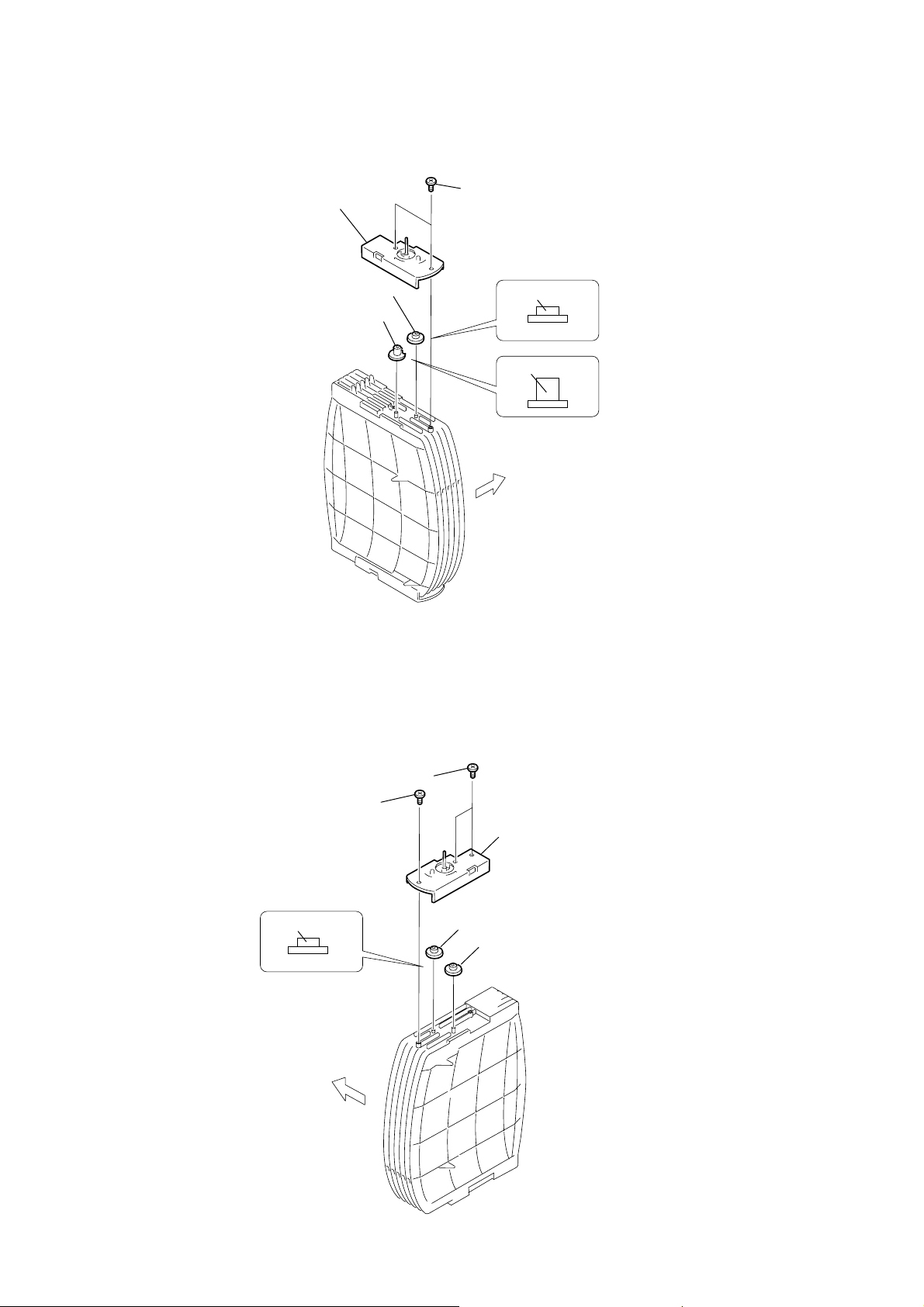
8-1. Side Plate, Top Panel Section ......................................... 103
8-2. Front Panel Section. .......................................................104
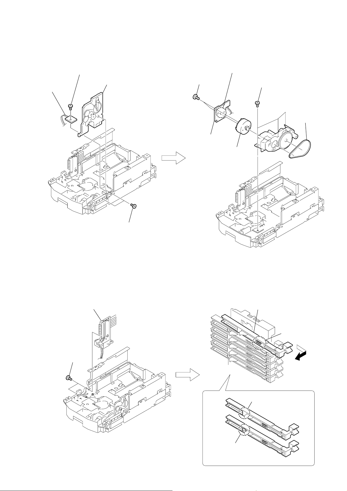
8-3. Chassis Section............................................................... 105
8-4. Rear Deck Section .......................................................... 106
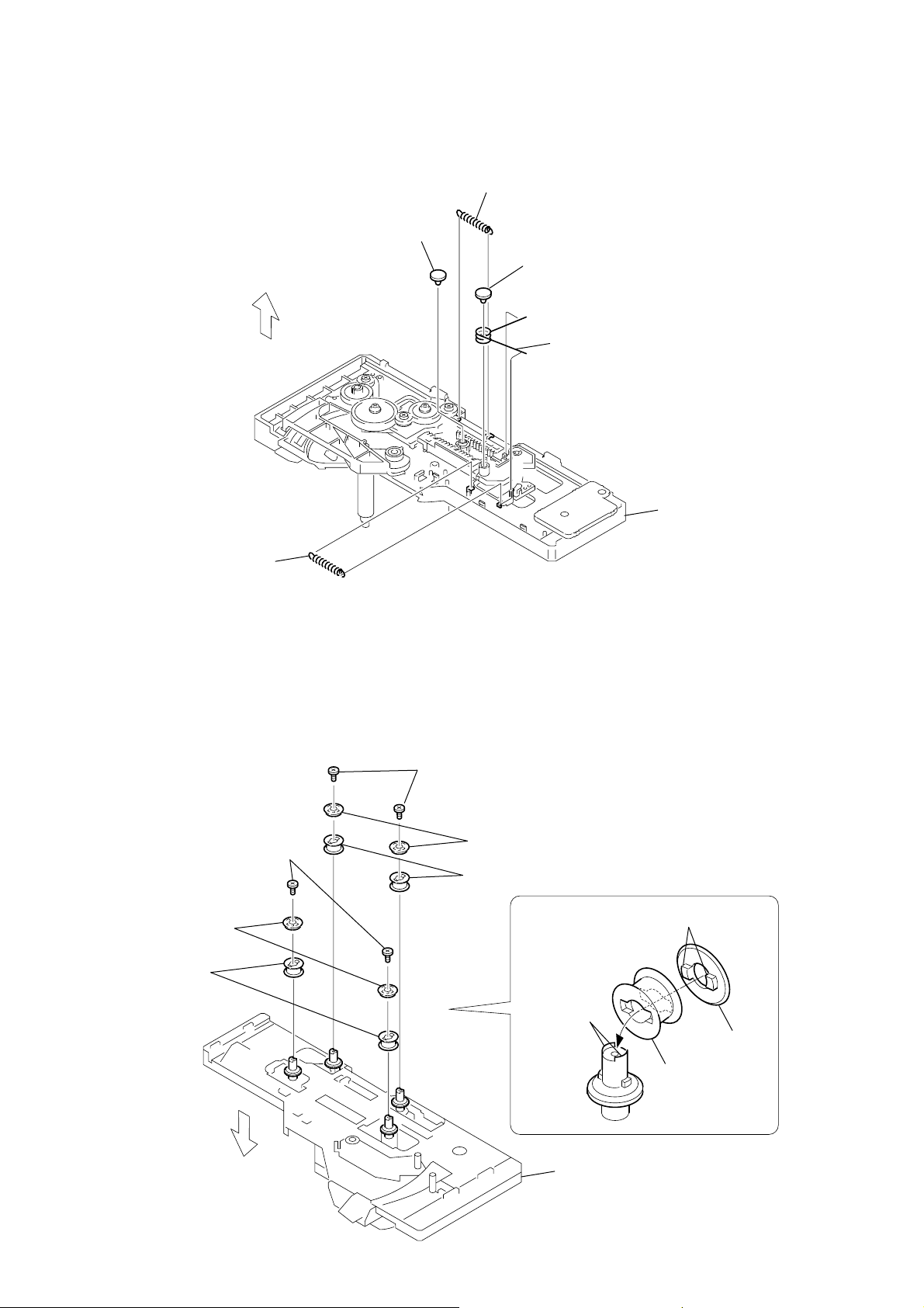
8-5. DVD Mechanism Deck Section-1
(CDM82B-DVBU28) ..................................................... 107
8-6. DVD Mechanism Deck Section-2
(CDM82B-DVBU28) .....................................................108
8-7. DVD Mechanism Deck Section-3
(CDM82B-DVBU28) .....................................................109
8-8. DVD Mechanism Deck Section-4
(CDM82B-DVBU28) ..................................................... 110
8-9. DVD Mechanism Deck Section-5
(CDM82B-DVBU28) ..................................................... 111
8-10. DVD Mechanism Deck Section-6
(CDM82B-DVBU28) ..................................................... 112
3
Page 4

HCD-HPX11D
8-11. DVD Mechanism Deck Section-7
(CDM82B-DVBU28) ..................................................... 113
8-12. DVD Mechanism Deck Section-8
(CDM82B-DVBU28) ..................................................... 114
8-13. DVD Mechanism Deck Section-9
(CDM82B-DVBU28) ..................................................... 115
8-14. DVD Mechanism Deck Section-10
(CDM82B-DVBU28) ..................................................... 116
8-15. Base Unit Section ........................................................... 117
9. ELECTRICAL PARTS LIST ................................ 118
4
Page 5

SECTION 1
SERVICING NOTES
HCD-HPX11D
NOTES ON HANDLING THE OPTICAL PICK-UP
BLOCK OR BASE UNIT
The laser diode in the optical pick-up block may suffer electrostatic
break-down because of the potential difference generated by the
charged electrostatic load, etc. on clothing and the human body.
During repair, pay attention to electrostatic break-down and also
use the procedure in the printed matter which is included in the
repair parts.
The flexible board is easily damaged and should be handled with
care.
NOTES ON LASER DIODE EMISSION CHECK
The laser beam on this model is concentrated so as to be focused on
the disc reflective surface by the objective lens in the optical pickup block. Therefore, when checking the laser diode emission,
observe from more than 30 cm away from the objective lens.
LASER DIODE AND FOCUS SEARCH OPERATION
CHECK
Carry out the “S curve check” in “CD section adjustment” and check
that the S curve waveforms is output three times.
• MODEL IDENTIFICATION
– Rear View –
Part No.
Model Name Part No.
SP and E3 models 4-255-426-0[]
EA model 4-255-426-1[]
AUS and TH models 4-255-426-2[]
•Abbreviation
AUS:Australian model
E3 : 240V AC area in E model
EA : Saudi Arabia model
SP : Singapore and Malaysia models
TH : Thai model
5
Page 6

HCD-HPX11D
12 3 4
q
q
q
q
q
q
Main unit
SECTION 2
GENERAL
This section is extracted
from instruction manual.
ALPHABETICAL ORDER
A – E F – Z
Cassette compartment 4
CD SYNC ws (36)
DIRECTION qj (35, 36, 37, 40,
54)
DISC 1 – 5, +1 wg (14, 17)
DISC SKIP 5 (14, 17)
Disc tray qs (12)
Display window 3
DSGX 6 (27, 37)
ECHO qh (39)
EQ EDIT qg (38)
EQ EDIT +/– qf (38)
EX-CHANGE w; (12, 14)
FUNCTION 9 (13, 18, 32, 33,
35, 48)
MIC VOL +/– qf (39)
PLAY MODE qj (13, 17, 18, 51)
Remote sensor 2
TUNER/BAND 0 (32, 33)
TUNING +/– 8 (32, 33)
TUNING MODE qj (32, 33)
VOLUME 7 (41, 50)
BUTTON DESCRIPTIONS
?/1 (power) 1 (9, 10, 33, 41, 42,
54)
lm/ML (skip back/
skip forward, rewind/fast
forward) 8 (14, 17)
x (stop) wf (14, 15, 35, 54)
z START (record) wd (36, 37,
40)
DVD/NX (play/pause) ql (13,
18, 51)
TAPE/hH (play) wa (35, 36,
37, 40)
Z (eject) qa (12, 14)
m
(mic) jack qd (39)
i
(phones) jack qk
wg
wf
wd
ws
wa
w;
ql
+/1
5
6
7
xz
lj JL
HShH
A
8
9
0
qa
qs
h
j
k
f
g
d
6
Page 7

Remote control
HCD-HPX11D
ALPHABETICAL ORDER
A – E
ALBUM + 7 (14, 17)
ALBUM – qa (14, 17)
ANGLE qk (25)
AUDIO qk (22)
BAND wg (32, 33)
CLEAR wl (18, 21)
CLOCK/TIMER SELECT e;
(42, 43, 50)
CLOCK/TIMER SET e; (10, 41,
42)
DISC SKIP wf (14, 17)
DISPLAY wa (43, 44, 45)
DVD DISPLAY wh (16, 17, 20,
22, 23, 25, 27, 45)
DVD MENU 7 (15)
DVD SETUP ws (11, 23, 25, 28
31, 54, 61)
DVD TOP MENU qa (15)
ENTER wj (10, 11, 15, 16, 17, 18,
20, 22, 25, 27, 31, 41, 54)
F – Z
FM MODE 5 (34, 53)
FUNCTION +/– 0 (13, 17, 32,
33, 35, 48)
KARAOKE/MPX qf (39)
#/2
KEY CONTROL
9 (39)
Number buttons qd (15, 16, 21,
24, 25, 28)
PLAY MODE 4 (13, 17, 18, 51)
REPEAT 5 (16)
SLEEP qh (41)
SOUND FIELD +/– wd (38)
SUBTITLE qk (23)
TUNER MEMORY 3 (32)
TUNING MODE 4 (32, 33)
TUNING +/– wk (32, 33)
TV CH +/– qg (9)
TV/VIDEO ea (9)
TV VOL +/– 2 (9)
VOLUME +/– 8 (41, 50)
BUTTON DESCRIPTIONS
?/1 (power) 1 (9, 10, 33, 41, 42,
54)
nN (play) 6 (13, 14, 15, 16,
17, 18, 30, 35, 51)
X (pause) 6 (14, 35)
x
(stop) 6 (14, 15, 35, 54)
>10* qs
TV ?/1 qj (9)
O RETURN ql (11, 16, 18, 21,
28, 29)
m (rewind) w; (14, 35)
M (fast forward) w; (14, 35)
SLOW /y w; (14)
M/m/</, wj (10, 14, 15, 16,
18, 20, 22, 25, 27, 31, 41, 42,
54)
. (go back) wk (14, 17)
> (go forward) wk (14, 17)
*This button does not funct ion.
ea
e;
wl
wk
wj
wh
wg
wf
qj
qh
+–+
–
qk
qf
+–+
–
qd
O
+–
y
y
mM.>
XbB
x
+
–
V
bB
+
v
–
+
+
–
–
ql
w;
wa
ws
qs
qa
O
+–
y
y
mM.>
XbB x
+–
V
bB
+
v
–
+
+
–
–
1
2qg
3
4
5
6
7
8
90
wd
7
Page 8

HCD-HPX11D
Setting the clock
Use buttons on th e remote for th e operation.
1
Press ?/1 to turn on the system.
2
Press CLOCK/TIMER SET.
3
Press M/m repeatedly to set the hour.
4
Press ENTER.
5
Press M/m repeatedly to set the
minute.
6
Press ENTER.
The clock start s working.
To adjust the clock
1 Press CL O CK/ TIMER SET.
2 Press M/m until “CLOCK SET” appears,
then press ENTER.
3 Do the same procedures as step 3 to 6
above.
Notes
•The clock settings are canceled when you disconnect
the power cord or if a power failure o ccurs.
•You cannot set the clock in Power Saving Mode.
8
Page 9

SECTION 3
DISASSEMBLY
•This is can be assemble according to the following sequence.
3-1. DISASSEMBLY FLOW-1
HCD-HPX11D
SET
3-3.OPTICAL PICK-UP BLOCK
(Page 11)
3-5.MECHANICAL DECK
(Page 13)
3-7.PANEL BOARD,
SUB PANEL BOARD,
HP BOARD,
MIC BOARD
(Page 14)
3-10.REAR PANEL,
DC FAN
(Page 16)
3-4.SIDE PLATE (L), (R),
TOP PANEL SECTION
(Page 12)
3-6.FRONT PANEL SECTION
(Page 14)
3-8.TUNER (FM/AM),
VIDEO BOARD,
SWITCHING REGULATOR,
MAIN HEAT SINK,
AMP BOARD
(Page 15)
3-9.MAIN BOARD,
POWER BOARD
(Page 16)
3-11.DMB07 BOARD,
POWER TRANSFORMER
(Page 17)
3-12.DVD MECHANISM DECK
(CDM82B-DVBU28),
FFC BOARD
(Page 18)
to DISASSEMBLY FLOW-2
9
Page 10

HCD-HPX11D
3-2. DISASSEMBLY FLOW-2
from DISASSEMBLY FLOW-1
3-13.PLATE (TOP)
(Page 19)
3-14. T OP SECTION
(Page 19)
3-15. ARM SECTION
(Page 20)
3-16. DVD MECHANISM DECK
SECTION (Page 21)
,
(L), (R)
3-25. SPR-E (ROLLER SLIDER UPPER)
(TOP SECTION) (Page 28)
3-17. SUB GEAR (2 STEP),
SUB SLIDER ASSY (Page 22)
3-18. ARM (R)
(Page 23)
3-19. GEAR (STOCK PLANET)
(RIGHT) (Page 24)
3-20. LEVER (SUB GEAR BACK L)
(Page 24)
3-21. ARM (L)
(Page 25)
3-22. GEAR (STOCK ROT LONG)
(LEFT) (Page 26)
3-26. RUBBER ROLLER
(TOP SECTION) (Page 28)
3-27. LOD MOTOR
(Page 29)
3-32. CHASSIS (TOP),
CHASSIS (BOTTOM) (Page 33)
3-33. LEVER
(LOADING R, LOADING L) (Page 34)
3-34. DISC STOP LEVER
(Page 35)
3-35. DRIVER BOARD
(Page 35)
3-23. GEAR (STOCK ROT SHORT)
(RIGHT) (Page 26)
3-24. STOCKER (1) ASSY TO
STOCKER (5) ASSY (Page 27)
3-28. SLIDER (PUSH-POPUP)
(Page 29)
3-36. RF BOARD
(Page 36)
3-37. OPTICAL PICK-UP
(DBU-3) (Page 36)
3-29. ROTARY ENCODER
(Page 30)
3-30. ASSEMBLING OF THE
ROTARY ENCODER (Page 31)
3-38. BASE UNIT SECTION
(Page 37)
3-39. LEVER (BU LOCK)
(Page 37)
3-40. GEAR (IDL-B)
(Page 38)
3-41. GEAR (IDL-C)
(Page 38)
3-31. ELV MOTOR
(Page 32)
3-42. SPR-E (TAKO-BACK)
(Page 39)
3-43. PLATE (PUSH) ASSY
(Page 40)
3-44. SPR-P (LOCK)
(Page 41)
10
Page 11

w
3-3. OPTICAL PICK-UP BLOCK
2
bottom cover plate
3
two screws
1
two screws
6
FFC board
5
HCD-HPX11D
4
w
ire (flat type)
29p(CN002)
q;
w
ire (flat type)
9p(CN003)
8
qa
9
w
ire (flat type)
24p(CN001)
7
two claws
RF board
qf
step screw
qk
insulator
ql
optical pick-up block
qg
qs
step scre
qh
insulator
qd
step screw
qj
insulator
11
Page 12

HCD-HPX11D
)
3-4. SIDE PLATE (L), (R), TOP PANEL SECTION
qs
top panel section
5
two screws
(BVTP3
7
side plate (L)
×
10
)
0
connector
(CN301)
8
two screws
(BVTP3
9
w
8p(CN302)
×
8
)
ire (flat type)
6
two screws
(BVTP3
qa
screw
(BVTP3
×
8
)
×
6
)
earth wire
3
sheet panel-T
When you exchange Side plate (R) assy,
please remove Sheet panel-T from old Side plate (R),
and attach in new Side plate (R).
4
side plate (R) assy
1
two screws
(BVTP3
2
two screws
(BVTP3
×
10
×
6
)
12
Page 13

T
3-5. MECHANICAL DECK
2
sheet (TC)
7
two screws
(BVTP2.6
HCD-HPX11D
1
four screws
(BVTP2.6
×
8
)
×
8
)
8
cassette shield plate
qa
leaf spring (cassette)
earth wire
6
two screws
(BVTP2.6
9
mechanical deck
qs
cassette panel
q;
×
8
)
3
two screws
(BVTP2.6
leaf spring (cassette)
5
cassette door
4
top panel
×
8
)
qd
sheet panel-
13
Page 14

HCD-HPX11D
3-6. FRONT PANEL SECTION
9
front panel section
3
screw
(KTP3
×
8
)
7
connector
6
w
ire (flat type) 17p(CN310)
(CN801)
earth wire
2
screw
(KTP3
×
8
)
4
CD panel
5
two screws
(BVTP3
×
6
)
3-7. PANEL BOARD, SUB PANEL BOARD, HP BOARD, MIC BOARD
4
w
ire (flat type)
2
five screws
(BVTP2.6
17p(CN801)
×
8
)
6
connector
(CN882)
8
connector
(CN306)
1
screw
(BVTP3
3
seven screws
(BVTP2.6
×
8
)
×
qf
PANEL board
5
7
HP board
q;
8
)
screw
(PWH2.6
four screws
(BVTP2.6
qa
(CN803)
×
10
)
×
8
connector
)
14
1
knob
(volume)
9
MIC board
qs
SUB PANEL board
qd
claw
8
screw
(PWH2.6
×
10
)
Page 15
qh
two screws
(
BVTP3
×
8)
5
four screws
(BVTP3
×
8
)
1
seven screws
(BVTP3
×
8
)
9
connector
(CN102)
6
board to board
connector
7
board to board
connector
3
claw
qk
connector
(CN601)
wa
connector
(CN502)
w;
connector
(CN501)
ql
connector
(CN602)
wj
AMP board
ws
four screws
(BVTP3
×
8
)
wd
four screws
(BVTP3
×
8
)
qf
connector
(CN201)
qg
connector
(CN101)
wh
Remove five
solderings
qj
SWITCHING REGULATOR
2
claw
8
w
ire (flat type) 17p(CN105)
qs
w
ire (flat type)
11p(CN305)
4
heat sink cover
q;
VIDEO board
qa
two screws
(BVTP3
×
8
)
qd
tuner (FM/AM
)
wk
SP board
wf
two screws
(
BVTP
3
×
16
)
wg
main heat sink
earth
HCD-HPX11D
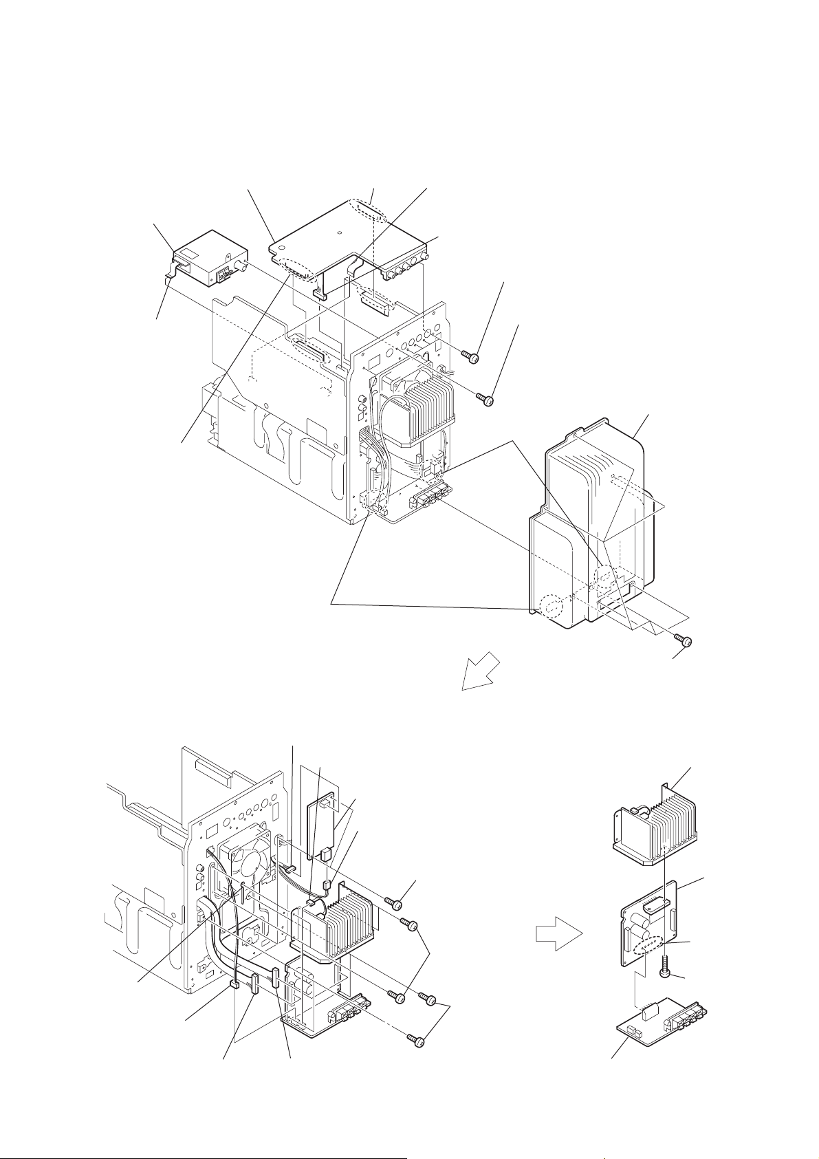
3-8. TUNER (FM/AM), VIDEO BOARD, SWITCHING REGULATOR, MAIN HEAT SINK, AMP BOARD
15
Page 16

HCD-HPX11D
)
3-9. MAIN BOARD, POWER BOARD
qg
four screws
(BVTP3
q;
two screws
(BVTP3
×
8
)
qf
connector
(CN1)
×
8
)
qs
connector
(CN52)
qa
(CN51)
connector
qd
connector
(CN3)
9
screw
(BVTP3
5
connector
(CN313)
3
(CN303)
×
8
)
connector
1
two screws
(BVTP3
×
8
4
w
ire (flat type)
(13p)(CN307)
8
)
MAIN board
qh
POWER board
3-10. REAR PANEL, DC FAN
6
w
ire (flat type)
(7p)(CN304)
2
7
w
ire (flat type)
(21p)(CN315)
two screws
(
TYPE2
3
2
two screws
(BVTP3
4
rear panel
×
30
)
3
DC fan
1
five screws
(BVTP3
×
8
)
×
8
16
Page 17

3-11. DMB07 BOARD, POWER TRANSFORMER
2
two screws
4
cover
3
two screws
6
four screws
(
BVTT
HCD-HPX11D
4
×
6
)
1
w
ire (flat type)
(29p)(CN501)
5
DMB07 board
7
power transformer
17
Page 18

HCD-HPX11D
3-12. DVD MECHANISM DECK (CDM82B-DVBU28), FFC BOARD
1
two screws
(BVTP3
×
6
)
2
sub chassis
1
two screws
(BVTP3
×
6
)
qa
w
ire (flat type)
21p (CN801)
5
two screws
(
M2.6 +BTTP
)
6
FFC cover
3
four screws
(BVTP3
×
4
chassis
7
(
9
29p (CN102)
qs
DVD mechanism deck
(CDM82B-DVBU28)
6
)
two screws
M2.6 +BTTP
8
FFC board
w
ire (flat type)
)
q;
w
ire (flat type)
29p (CN801)
18
Page 19
)
3-13. PLATE (TOP), (L), (R)
2
gear (joint op), shaft (stock)
7
screw
(BTTPM 2.6
3
four screws
(BTTPM 2.6
8
plate (cam R)
×
8)
×
HCD-HPX11D
8)
4
plate (cover top)
3-14. TOP SECTION
3
two screws
×
(BTP 2
8)
shock guard
(lower)
1
screw (BTP 2
2
gear (connection tp)
×
8)
4
two screws
(PTPWH 2
7
top section
×
14)
1
gear (joint op)
6
plate (cam L)
5
(BTTPM 2.6
6
shock guard
(lower)
5
claw
screw
×
8
8
shaft (connection)
19
Page 20

HCD-HPX11D
3-15. ARM SECTION
2
Slide the arm section in the
direction of the arrow B.
B
T
urn over the
1
in the direction of the arrow
pulley (LOD motor)
A
A
.
5
Remove the
in the direction of the arrow D.
D
arm section
6
arm section
3
claw
C
4
Pull this portion with a finger
in the direction of the arrow C.
20
Page 21

3-16. DVD MECHANISM DECK SECTION
pulley (ELV motor)
3
cover
B
1
two screws
HCD-HPX11D
2
two screws
A
4
T
urn over the
in the direction of the arrow A.
pulley (ELV motor)
plate (cam L)
5
Slide the
in the direction of the arrow
6
four
claws
7
Remove the DVD mechanism deck section
in the direction of the arrow C.
C
DVD mechanism deck section
B
.
21
Page 22

HCD-HPX11D
3-17. SUB GEAR (2 STEP), SUB SLIDER ASSY
9
Remove the
in the direction of the arrow.
sub slider assy
0
sub slider assy
5
sub gear (2 step)
sub slider assy
4
sub gear (idler)
1
k tapping screw (K2.6
3
2
two screws (M2
×
8)
cover (R)
×
5)
22
6
7
sub gear (idler)
8
sub gear (idler)
sub gear (idler)
Page 23
)
3-18. ARM (R)
3
lever (sub gear back R)
1
sub gear (joint just front)
2
SPR-T (sub gear back R)
HCD-HPX11D
7
gear (stock joint)
6
gear (stock rotary right)
5
gear (sub gear pin right
4
two washers (5.5)
9
arm (R)
8
two screws
× 5
(K2
)
23
Page 24
HCD-HPX11D
)
)
3-19. GEAR (STOCK PLANET) (RIGHT)
1
two screws (BTTP M2.6
2
stock base (A)
3
gear (stock sun)
4
gear (stock planet)
×
6
3-20. LEVER (SUB GEAR BACK L)
5
gear (stock joint),
shaft (stock)
UPPER
SIDE
2
screw (M2
1
3
6
7
lever (sub gear back L)
4
sub gear (joint just front)
×
5)
screw (K2.6
cover (L)
SPR-T (sub gear back L
×
8)
24
Page 25

)
3-21. ARM (L)
4
arm (L), stock base (B)
1
two washers (5.5)
UPPER
SIDE
HCD-HPX11D
2
gear (sub gear pin right
3
gear (stock rotary right)
6
gear (stock sun)
5
gear (stock planet)
UPPER
SIDE
25
Page 26
HCD-HPX11D
)
3-22. GEAR (STOCK ROT LONG) (LEFT)
2
stock box (L)
3
gear (stock rot short)
4
gear (stock rot long)
1
two screws (2
short
long
UPPER
SIDE
×
6)
3-23. GEAR (STOCK ROT SHORT) (RIGHT)
1
two screws (2
2
screw (1.7)
short
UPPER
SIDE
×
6)
3
stock box (R)
4
gear (stock rot short)
5
gear (stock rot short
26
Page 27

3-24. STOCKER (1) ASSY TO STOCKER (5) ASSY
UPPER
SIDE
1
dowel
2
claw
HCD-HPX11D
3
Remove the stocker
in the direction of the arrow.
(1) assy
Repeat the steps 1 to 3, when removing the part
(2), (3), (4) and (5) of the stocker assy.
4
stocker (1) assy
5
stocker (2) assy
UPPER
SIDE
6
stocker (3) assy
7
stocker (4) assy
8
stocker (5) assy
27
Page 28
HCD-HPX11D
3-25. SPR-E (ROLLER SLIDER UPPER) (TOP SECTION)
5
bushing
UPPER
SIDE
3
SPR-E (8 cm slider L)
1
bushing
2
SPR-T (8 cm slider R)
4
SPR-E
(roller slider upper)
3-26. RUBBER ROLLER (TOP SECTION)
4
two screws
(2
×
5)
5
two parasols
1
two screws
(2
×
5)
2
two parasols
3
two
rubber rollers
top section
two claws
28
6
two
rubber rollers
UPPER
SIDE
two claws
parasol
rubber roller
top section
Page 29
)
3-27. LOD MOTOR
2
screw
(BTTPM 2.6
3
SW (B) board
×
8)
4
sub chassis assy (L)
7
two screws
(BTTP M2.6
9
MOTOR LOD board
×
8
Remove soldering from the two points
5
8)
q;
LOD motor
three screws
(BTTP M2.6
HCD-HPX11D
×
8)
6
belt (MOT-OP
1
(BTTP M2.6
3-28. SLIDER (PUSH-POPUP)
2
sub chassis assy (R),
diskadress sw board
1
two screws
(BTTP M2.6
×
8)
two screws
×
8)
4
Remove the slider (push-popup1)
in the direction of the arrow.
3
claw
slider (push-popup 1)
slider (push-popup 2)
29
Page 30

HCD-HPX11D
3-29. ROTARY ENCODER
6
Rotate the
the hole on the chassis can be seen
through the plate (comR).
ELV
motor until the position for
plate (com R)
1
three screws
(BTTP M2.6
×
6)
4
TRANSLATION board
2
connector (CN805)
3
connector (CN808)
7
screw
(PTPWH2.6
9
screw
(PTPWH2.6
qa
screw
(PTPWH2.6
qd
screw
(PTPWH2.6
qg
step tapping screw
(PWH2
×
×
6)
×
8)
5
Rotate the ELV motor in
the direction of the arrow.
×
8)
8
×
8)
8)
q;
qs
gear (geneva 1)
qf
gear (encoder)
gear (pulley UD)
gear (geneva 2)
30
qh
Remove soldering
from the five points
qk
rotary encoder
qj
two claws
Page 31

3-30. ASSEMBLING OF THE ROTARY ENCODER
4
screw
(PTPWH2.6
2
two claws
3
Apply the soldering
in five points.
8
screw
(PTPWH2.6
gear (encoder)
5
gear (encoder)
×
HCD-HPX11D
8)
×
8)
1
rotary encoder
9
screw
(PTPWH2.6
6
gear (geneva 1)
×
8)
rotary encoder
qd
Align the plate (com R)
and the chassis hole.
7
gear (geneva 2)
gear (geneva 1)
gear
(geneva 1)
Adjust phases.
qa
Adjust phases.
qh
screw
(PTPWH2.6
qg
gear (pulley UD)
×
qs
screw
(PTPWH2.6
0
gear (geneva 2)
8)
×
8)
qf
Align the plate (com L)
and the chassis hole.
plate (com R)
plate (com L)
31
Page 32

HCD-HPX11D
3-31. ELV MOTOR
2
two screws
(BTTP M2.6
4
ELV MOTOR board
5
ELV
×
8)
motor
3
Remove soldering
from the five points
1
belt (MOT-UD)
belt (MOT-UD)
UPPER
SIDE
32
Page 33

)
3-32. CHASSIS (TOP), CHASSIS (BOTTOM)
4
three screws
3
two screws
(P2
5
chassis (top)
(BVTP2.6
×
10)
×
8)
1
screw
(BVTP2.6
2
lever (CL UP2)
HCD-HPX11D
×
8)
7
chassis (bottom
6
four screws
(P3
×
10)
33
Page 34

HCD-HPX11D
)
3-33. LEVER (LOADING R, LOADING L)
6
lever (loading R)
2
SPR-T (loading L) SPR-T (loading R)
5
two hooks
1
3
two hooks
PRECAUTION DURING LEVER (LOADING R/L) INSTALLATION
Align the horizontal position.
lever (loading L)
Install the
both levers so that they move symmetrically.
lever (loading R)
4
lever (loading L
34
Page 35

3-34. DISC STOP LEVER
d
5
two hooks
1
gear (cap)
2
gear (IDL L)
HCD-HPX11D
PRECAUTION DURING DISC STOP LEVER INSTALLATION
hole
chassis (top)
6
disc stop lever
3-35. DRIVER BOARD
3
Remove soldering
from the two points.
4
motor (pulley) assy
(LOD)
3
two claws
4
disc sensor lever
disc stop lever
hole
Install the disc stop lever so that the both holes
are aligned.
2
two screws
(BVTP2.6 × 8)
5
DRIVER boar
1
belt (MOT)
35
Page 36

HCD-HPX11D
s
3-36. RF BOARD
2
wire (flat type)
24p (CN001)
5
RF board
4
Remove soldering
from the two points.
1
wire (flat type)
9p (CN003)
3-37. OPTICAL PICK-UP (DBU-3)
2
(PTPWH M2.6)
floating screw
3
claw
1
two
floating screws
(PTPWH M2.6)
3
two insulator
36
4
i
nsulator
5
optical pick-up
(DBU-3)
Page 37

r
3-38. BASE UNIT SECTION
4
Remove the base unit
in the direction of the arrow.
2
f
loating screw
(PTPWH M2.6)
1
HCD-HPX11D
SPR-E 213 down holde
3-39. LEVER (BU LOCK)
5
lever (BU lock)
2
gear (BU lock)
1
f
loating screw
(PTPWH M2.6)
3
floating screw
(PTPWH M2.6)
4
three hooks
3
37
Page 38

HCD-HPX11D
3-40. GEAR (IDL-B)
2
claw
1
DIR spring
9
DIR lever
3
gear pulley
4
gear (cap)
5
gear (IDL-A)
q;
gear (IDL B long)
8
stopper
6
Loosen the screw.
7
Hold the Release lever
and change the direction.
3-41. GEAR (IDL-C)
3
gear (IDL-D)
2
two claws
1
gear (IDL-F)
7
gear (IDL-C)
4
three hooks
5
gear loading lever
38
6
claw
Page 39

)
3-42. SPR-E (TAKO-BACK)
two claws
HCD-HPX11D
two claws
parasol
rubber roller
3
four
rubber rollers
1
four screws (2 × 5)
2
four parasols
5
SPR-E (tako-back)
4
tension spring (lower
39
Page 40

HCD-HPX11D
3-43. PLATE (PUSH) ASSY
5
Remove the
in the direction of the arrow.
plate (push) assy
4
four claws
1
SPR-E (plate-push-back)
2
screw (PTPWH M2)
3
gear (tako second)
PRECAUTION DURING GEAR (TAKO SECOND) INSTALLATION
3
SPR-E (plate-push-back)
2
four claws
1
Remove the
in the direction of the arrow.
plate (push) assy
Adjust phases.
plate (push) assy
5
Adjust phases.
plate (push) assy
gear (tako second)
4
gear (tako second)
40
Page 41

3-44. SPR-P (LOCK)
1
claw
2
lever (lock)
3
SPR-P (lock)
HCD-HPX11D
PRECAUTION DURING LEVER INSTALLATION
2
Hold the both ends of the SPSR-P
(lock) with two claws.
1
SPR-P (lock)
3
lever (lock)
4
Pick up the SPR-P (lock) from
the claw and hook it on the lever.
41
Page 42

HCD-HPX11D
SECTION 4
ASSEMBLY
•This is can be assemble according to the following sequence.
4-1. ASSEMBLY FLOW
4-2. ASSEMBLING OF THE
STOCKER SECTION (Page 43)
4-3. ASSEMBLING OF THE GEAR
(STOCK RO T SHOR T) (RIGHT) (Page 44
4-4. ASSEMBLING OF THE GEAR
(STOCK RO T LONG) (LEFT) (P age 45)
4-5. CONFIRMING THE ASSEMBLING
OF THE STOCKER SECTION (Page 46)
4-6. ASSEMBLING OF THE GEAR
(STOCK RO TARY LEFT) (Page 47)
4-7. ASSEMBLING OF THE GEAR
(STOCK RO TARY RIGHT) (Page 48)
4-8. ASSEMBLING OF THE LEVER
(SUB GEAR BACK L) (Page 49)
4-9. ASSEMBLING OF THE GEAR
(SUB GEAR PIN RIGHT) (Page 50)
4-10. ASSEMBLING OF THE LEVER
(SUB GEAR BACK R) (Page 51)
4-11. ASSEMBLING OF THE
SUB GEAR (IDLER) (Page 52)
4-12. ASSEMBLING OF THE
SUB GEAR (2 STEP) (Page 53)
4-13. CONFIRMING THE ASSEMBLING
OF THE ARM SECTION (Page 54)
42
Page 43

4-2. ASSEMBLING OF THE STOCKER SECTION
1
Check the number on each stocker assy,
before assembling all the assys.
HCD-HPX11D
2
stocker (1) assy
6
stocker (1) assy
7
stocker (2) assy
UPPER
SIDE
3
stocker (2) assy
5
two claws
4
two dowels
8
stocker (3) assy
9
stocker (4) assy
0
stocker (5) assy
1
Repeat the steps 4 to 6, when installing the part
(2), (3), (4) and (5) of the stocker assy.
43
Page 44

HCD-HPX11D
4-3. ASSEMBLING OF THE GEAR (STOCK ROT SHORT) (RIGHT)
7
short
two screws (2
8
screw (1.7)
UPPER
SIDE
×
6)
Note:
Install the stock box (R) right after
finishing the phase adjustment.
4
gear (stock rot short)
2
gear (stock rot short)
6
stock box (R)
PRECAUTION DURING GEAR (STOCK ROT SHORT) INSTALLATION
1
Align the edges of the stockers. Keep the position of
the stockers until finishing installation of the gear
(stock rot short) and the stock box (R).
FRONT
SIDE
gear (stock rot short)
3
Adjusting the one stockers
44
5
Adjusting the two stockers
gear (stock rot short)
Page 45

4-4. ASSEMBLING OF THE GEAR (STOCK ROT LONG) (LEFT)
6
two screws (2
2
gear (stock rot short)
4
gear (stock rot long)
×
6)
HCD-HPX11D
Note.
Install the stock box (L) right after finishing
the phase adjustment.
7
stocker box (L)
short
long
UPPER
SIDE
PRECAUTION DURING
(STOCK ROT SHORT, STOCK ROT SHORT LONG)
1
Align the edges of the stockers. Keep the position of
the stockers until finishing installation of the gear
(stock rot short) and the stock box (L).
GEAR
INSTALLATION
FRONT
SIDE
5
Adjusting the one stockers
3
Adjusting the two stockers
gear (stock rot long)
gear (stock rot short)
45
Page 46

HCD-HPX11D
4-5. CONFIRMING THE ASSEMBLING OF THE STOCKER SECTION
stocker section
UPPER
SIDE
STOCKER ASSY (R) SIDE
3
Confirm that each claw contacts uniformly at the
respective stop positions of the stocker assy (1) to the stocker assy (5).
4
Confirm the stocker assys move smooth
by sliding the stocker assys (1) to (5)
FRONT
SIDE
Slide the stocker assy in the
1
direction of the arrow.
UPPER
SIDE
46
STOCKER ASSY (L) SIDE
FRONT
SIDE
2
Confirm that each claw contacts uniformly at the
respective stop positions of the stocker assy (1) to the stocker assy (5).
Page 47

4-6. ASSEMBLING OF THE GEAR (STOCK ROTARY LEFT)
2
gear (stock sun)
4
gear (stock planet)
UPPER
SIDE
PRECAUTION DURING GEAR (STOCK PLANET) INSTALLATION
1
Align the edges of stockers,
and keep the position.
FRONT
SIDE
HCD-HPX11D
3
Position to adjust phases
for the gear (stock sun).
Position to adjust phases
5
for the gear (stock planet)
6
Move the arm (L) and the stock
base (B) vertically to the gear.
UPPER
SIDE
7
Check if the stock base (B) is kept
parallel with groove of the stocker.
0
Align the edges of stockers,
and keep the position.
8
gear (stock rotary left)
9
washer (5.5)
The cut-off curve should
face to the front.
47
Page 48

HCD-HPX11D
4-7. ASSEMBLING OF THE GEAR (STOCK ROTARY RIGHT)
0
gear (stock rotary right)
UPPER
SIDE
1
Turn over the
in the direction of the arrow.
stocker assy
qa
washers (5.5)
The cut-off curve should
face to the front.
3
Check that these faces are positioned
parallel to each other.
PRECAUTION DURING GEAR
(STOCK PLANET) INSTALLATION
4
gear (stock sun)
6
gear (stock planet)
5
Position to adjust phases
for the gear (stock sun).
8
stock base (A)
9
two screws
(BTTP M2.6
×
6)
48
2
Keep the position of the edges of
the stockers and adjust phases.
FRONT
SIDE
7
Position to adjust phases
for the gear (stock planet).
Page 49

4-8. ASSEMBLING OF THE LEVER (SUB GEAR BACK L)
1
Turn over the
stocker assy
in the direction of the arrow.
2
Adjust phases.
gear (stock rotary left)
gear (sub gear pin left)
3
gear (sub gear pin left)
4
washers (5.5)
qa
k tapping screw
(2.6
×
8)
0
screw (M2
×
5)
9
cover (L)
7
lever
(sub gear back L)
8
SPR-T
(sub gear back L)
SPR-T (sub gear back L)
gear (stock rotary left)
sub gear (joint just front)
6
lever (joint just front)
gear (sub gear pin left)
5
gear (stock joint),
shaft (stock)
lever (sub gear back L)
PRECAUTION DURING SPR-T
(SUB GEAR BACK L) INSTALLATION
PRECAUTION DURING GEAR
(SUB GEAR PIN LEFT) INSTALLATION
UPPER
SIDE
HCD-HPX11D
49
Page 50

HCD-HPX11D
4-9. ASSEMBLING OF THE GEAR (SUB GEAR PIN RIGHT)
1
Turn over the
in the direction of the arrow.
stocker assy
PRECAUTION DURING GEAR
(SUB GEAR PIN RIGHT) INSTALLATION
UPPER
SIDE
2
Remove the
in the direction of the arrow.
arm (R)
4
two screws
(2
× 5
gear (sub gear pin right)
6
Adjust phases.
gear (stock rotary right)
)
5
gear (sub gear pin right)
gear (stock joint)
7
washers (5.5)
50
3
two dowels
Page 51

4-10. ASSEMBLING OF THE LEVER (SUB GEAR BACK R)
1
sub (joint just front)
2
gear (stock joint)
Note:
Put the driver on the bottom of the other side of the gear,
and push the gear (stock joint) into it. Confirm it is
attached securely .
HCD-HPX11D
PRECAUTION DURING SPR-T
(SUB GEAR BACK R) INSTALLATION
3
claw
5
SPR-T (sub gear back R)
4
lever (sub gear back R)
SPR-T (sub gear back R)
gear (stock rotary right)
gear (sub gear pin right)
claw
lever (sub gear back R)
51
Page 52

HCD-HPX11D
4-11. ASSEMBLING OF THE SUB GEAR (IDLER)
1
of the arrow A until it stops.
4
Position to adjust phases
for the sub gear (idler).
A
Push the sub slider assy in the direction
2
The place that the sub slider assy
stops outside of this.
sub slider assy
3
sub gear (idler)
Note.
The side which has a pattern is the bottom.
4
three sub gears (idler)
Note.
The side which has a pattern is the bottom.
No need of phase adjustment.
52
Page 53

4-12. ASSEMBLING OF THE SUB GEAR (2 STEP)
HCD-HPX11D
gear (sub gear pin right)
1
sub gear (2 step)
hole
hole
hole
PRECAUTION DURING SUB GEAR (2 STEP) INSTALLATION
2
Align the
the
sub gear (2 step)
sub gear (2 step)
gear (sub gear pin right)
gear (sub gear pin right)
and
hole.
5
two screws (M2
4
k tapping screw (2.6
×
5)
3
cover (R)
×
8)
6
arm section
53
Page 54

HCD-HPX11D
4-13. CONFIRMING THE ASSEMBLING OF THE ARM SECTION
2
Check point 1:
The smooth movement of
this part when sliding.
1
Release the lock of the sub slider assy
and slide it in the direction of the arrow.
UPPER
SIDE
Note.
If the two parts of the stopper do not touch the stock base (B) when
the sub slider assy is pushed to the end, the phases are not correctly
adjusted. Reassemble the assy.
6
Check point 3:
Two parts of the stopper
touch the stock base (B).
5
Push the sub slider
assy into the end of
the arm (R).
stock base (B)
3
Check point 2:
All the stocker assy is standing.
4
Slide the stocker assy in the
direction of the arrow.
54
Page 55

SECTION 5
TEST MODE
HCD-HPX11D
[Cold Reset]
• The cold reset clears all data including preset data stored in
the RAM to initial conditions. Execute this mode when
returning the set to the customer.
Procedure:
1. Press ?/1 button to turn the set ON.
2. Press three buttons x , PLAY MODE / TUNING MODE ,
and ?/1 simultaneously.
3. The fluorescent indicator tube does not display any message
and the set is reset.
[Tuner Step Change]
•A step of AM channels can be changed over between 9 kHz
and 10 kHz.
Procedure:
1. Press ?/1 button to turn the set ON.
2. Select the function “TUNER”, and press TUNER/BAND
button to select the BAND “AM”.
3. Press ?/1 button to turn the set OFF.
4. Press +ML and ?/1 buttons simultaneously, and the
display of fluorescent indicator tube changes to “STEP 9” or
“STEP 10”, and thus the channel step is changed over.
[Function Change]
• Change of function VIDEO or MD (also the input level
changes).
Procedure:
1. Press ?/1 button to turn the set ON.
2. Press FUNCTION and ?/1 buttons simultaneously, and
the display of fluorescent indicator tube changes to “MD” or
“VIDEO”, and thus the channel step is changed over.
3. Press ?/1 button to turn the set OFF.
[DISC TRA Y LOCK]
The disc tray lock function for the antitheft of a demonstration
disc in the store is equipped.
Setting Procedure :
1. Press the ?/1 button to turn the set on.
2. Press two buttons of x and Z simultaneously for five
seconds.
3. The message “LOCKED” is displayed and the tray is locked.
Releasing Procedure :
1. Press two buttons of x and Z simultaneously for five
seconds.
2. The message “UNLOCKED” is displayed and the tray is
unlocked.
Note : When “LOCKED” is displayed, the tray lock is not released by
turning power on/off with `/1 button.
[P ANEL Test Mode]
•This mode is used to check the version, FL tube, LED and
keyboard.
Procedure:
1. Press ?/1 button to turn the set ON.
2. Press three buttons x , DSGX , and ECHO simultaneously.
3. LEDs and fluorescent indicator tube are all turned on.
[COMMON (MC) Test Mode]
•This mode is used to check operations of the respective sections
of Amplifier, T uner, and Tape.
Procedure:
•To enter COMMON (MC) Test Mode
1. Press ?/1 button to turn on the set.
2. Press the three buttons of x , PLAY MODE / TUNING
MODE and DSGX simultaneously.
3. When VOLUME control knob is turned clockwise even
slightly, the sound volume increases to is maximum and a
message “VOLUME MAX” appears for two seconds, then
the display returns to the original display.
4. When VOLUME control knob is tuned counter-clockwise
even slightly, the sound volume decreases to its minimum and
a message “VOLUME MIN” appears for two seconds, then
the display returns to the original display.
5. When you press the EQ EDIT button, the message “GEQ
MAX” is displayed and the entire band of the graphic equalizer
is set to the maximum level.
6. When you press the EQ EDIT button, the message “GEQ
MIN” is displayed and the entire band of the graphic equalizer
is set to the minimum level.
7. When you press the EQ EDIT button, the message “GEQ
FL T” is displayed and the entire band of the graphic equalizer
is set to the center level.
8. When you want to exit this mode, press ?/1 button.
9. The cold reset is enforced at the same time.
[Color System Change]
Procedure:
1. Press ?/1 and lm– buttons simultaneously, and the
display of fluorescent indicator tube changes to “COL PAL”
or “COL NTSC”, and the color system is changed over.
[DVD and CD Ship Mode (No Memory Clear)]
•This mode moves the position to the position durable to vibration Use this mode when returning the set to the customer
after repair.
Procedure:
1. Press ?/1 button to turn the set ON.
2. Press three EX-CHANGE button and ?/1 button
simultaneously.
3. After the “STANBY” display blinks six times, a message
“LOCK” is displayed on the fluorescent indicator rube, and
the DVD ship mode is set.
[DVD and CD Ship Mode (Memory Clear)]
•This mode moves the pick-up to the position durable to vibration. Use this mode when returning the set to the customer
after repair.
Procedure:
1. Press ?/1 button to turn the set ON.
2. Press three buttons EX-CHANGE , Z , and PLAY MODE
/ TUNING MODE button simultaneously.
3. After the “STANDBY” display blinks six times, a message
“LOCK” is displayed on the fluorescent indicator tube, and
the DVD ship mode is set.
55
Page 56

HCD-HPX11D
[Ver sion Test Mode]
Procedure:
1. When the panal test mode is activated, press the DISC1 button
and the model name and destination is displayed one after the
other.
2. Whenever press the DISC1 button, the version is displayed
in order of MC, GC, ST, TA, TM, TC and DVD.
3. Press the DISC3 button and the date of the software production
is displayed.
4. Press the DISC3 button again and the version is displayed.
5. To exit from this mode, press three buttons x , DSGX and
ECHO simultaneously.
[Key T est Mode]
Procedure:
1. When the panel test mode is activated, press the DISC2 button,
to select the key test mode. In the key check mode, the
fluorecent indicator displays “K 0 V0”. Each time a b utton is
pressed, “K” value increases. However, once a button is
pressed, it is no longer taken into account. When all keys are
pressed correctly, “K25 V0” is displayed.
2. To exit from this mode, press three buttons x , DSGX and
ECHO simultaneously.
[DVD Power Manage]
Procedure:
1. Press the ?/1 button to turn the set on.
2. Select the FUNCTION to DVD.
3. Press the ?/1 button to turn off the main power.
4. While depressing the x button, press the ?/1 button.
5. The message “DVD POWER OFF” is displayed.
6. Press the ?/1 button to turn off the main power.
7. Repeat step 1 to 4.
8. The message “DVD POWER ON” is displayed.
[DVD Service Mode]
Procedure:
1. Press the ?/1 button on the main unit.
2. Set the FUNCTION to DVD.
3. Press three buttons of Z , x and MIC VOL + simultaneously .
4. The message “SERVICE IN” is display ed on the display. The
Test Mode Menu is displayed.
5. To execute each function, select the number on the remote
commander.
6. See the following section for explanation in detail.
7. To exit from this mode, press the ?/1 button.
56
Page 57

SECTION 6
test tape
P-4-A100
(10 kHz, –10 dB)
oscilloscope
set
Waveform of oscilloscope
in phase 45
°
90
°
135
°
180
°
good
wrong
R-ch
L-ch
VH
Pin
3
(GND)
MAIN board
CN301
Pin
2
(L-CH)
Pin 4 (R-CH)
ELECTRICAL ADJUSTMENTS
HCD-HPX11D
TAPE SECTION 0 dB=0.775V
1. Demagnetize the record/playback head with a head
demagnetizer.
2. Do not use a magnetized screwdriver for the adjustments.
3. After the adjustments, apply suitable locking compound to
the parts adjusted.
4. The adjustments should be performed with the rated power
supply voltage unless otherwise noted.
5. The adjustments should be performed in the order given in
this service manual. (As a general rule, playback circuit
adjustment should be completed before performing recording
circuit adjustment.)
6. The adjustments should be performed for both L-CH and RCH.
7. Switches and controls should be set as follows unless otherwise
specified.
Tape
P-4-A100
WS-48B
Record/Playback Head Azimuth Adjustment
Procedure :
1. Mode : Playback
test tape
P-4-A100
(10 kHz, –10 dB)
Signal Used for
10 kHz, –10 dB
3 kHz, 0 dB
MAIN board
CN301
2
Pin
4
Pin
Azimuth Adjustment
Tape Speed Adjustment
(L-CH) or
(R-CH)
level meter
3. Mode: Playback
4. After the adjustments, apply suitable locking compound to
the parts adjusted.
Adjustment Location: REC/PB Head
Tape Speed Check
Procedure :
1. MODE : FWD Playback.
set
Pin
3
(GND)
+
–
2. Turn the adjustment screw and check output peaks. If the peaks
do not match for L-CH and R-CH, turn the adjustment screw
so that outputs match within 1 dB of peak.
L-CH
peak
screw
position
R-CH
peak
output
level
within
1 dB
L-CH
peak
R-CH
peak
within 1dB
screw
position
set
MAIN board
CN301
Pin
2
(L-CH) or
Pin
4
(R-CH)
Pin
3
(GND)
frequency
counter
test tape
WS-48B
(3 kHz, 0 dB)
2. Insert the WS-48B into deck.
3. Press the TAPE hH button of deck.
4. Check the reading of frequency counter becomes 3000 ± 90
Hz.
Sample Value of Wow and flutter
W.RMS (JIS) less than 0.35%
(test tape: WS-48B)
57
Page 58

HCD-HPX11D
e
DVD SECTION
About the dicision to pass or fail of the optical pick-up block.
TEST DISC LIST
Use the following test disc on test mode.
LUV-P01 (CD): PART No. 4-999-032-01
TDV-520CSO (DVD-SL): PART No. J-2501-236-A
TDV-540C (DVD-DL): PART No. J-2501-235-A
Note: Do not use exiting test disc for DVD.
AUTO SERVO ADJUSTMENT
After parts related to the servo circuit (RF amplifier (IC001), DSP
(IC509), motor driver (IC501), EEPROM (IC903) so on) are
replaced, re-adjusting the servo circuit is necessary. Select “ALL”
at “1. DRIVE AUTO ADJUSTMENT” (Refer to page 2 in DVD
Service Mode) and adjust DVD-SL (single layer), CD and DVDDL (dual layer).
VIDEO SECTION
Video Level Check (VIDEO BOARD)
Purpose
This adjustment is made to satisfy the NTSC standard, and if not
adjusted correctly, the brightness will be too large or small.
oscilloscop
Ω
75
set
J703
VIDEO OUT jack
Procedure :
1. Connect oscilloscope to VIDEO output.
2. Load a DVD reference disc playback.
3. Check the video signal level is 1.00 ± 0.05Vp-p.
1.00 ± 0.05 Vp-p
(WHITE 100%)
58
Page 59

• Circuit Boards Location
HCD-HPX11D
SECTION 7
DIAGRAMS
PANEL board
HP board
POWER board
SWITCHING
REGULATOR
VIDEO board
THERMISTOR board
AMP board
SPEAKER board
FFC board
MAIN board
SUB PANEL board
DISC ADDRESS SW board
ELV MOTOR board
SW (C) board
MIC board
SW (D) board
DMB07 board
DRIVER board
SW (A) board
RF board
MOTOR LOD board
SW (B) board
TRANSLATION board
59
Page 60

HCD-HPX11D
NOTE FOR PRINTED WIRING BOARDS AND SCHEMATIC DIAGRAMS
Note on Printed Wiring Boards:
• X : parts extracted from the component side.
• Y : parts extracted from the conductor side.
• W : indicates side identified with part number.
• f : internal component.
• : Pattern from the side which enables seeing.
(The other layers' patterns are not indicated.)
Caution:
Pattern face side: P arts on the pattern face side seen from
(Side A) the pattern face are indicated.
Parts face side: Parts on the parts face side seen from
(Side B) the parts face are indicated.
• Indication of transistor.
C
Q
B
E
B
B
These are omitted.
Q
CE
These are omitted.
Q
CE
These are omitted.
Note on Schematic Diagram:
• All capacitors are in µF unless otherwise noted. (p:
pF)
50 WV or less are not indicated except for electrolytics
and tantalums.
•All resistors are in Ω and 1/
wise specified.
• f : internal component.
• 2 : nonflammable resistor.
• 5 : fusible resistor.
• C : panel designation.
Note: The components identified by mark 0 or dotted
line with mark 0 are critical for safety.
Replace only with part number specified.
• A : B+ Line.
• B : B– Line.
•Voltages and wavef orms are dc with respect to ground under no-signal conditions.
•Voltages are taken with a VOM (Input impedance 10 MΩ).
Voltage variations may be noted due to normal production
tolerances.
•Waveforms are taken with a oscilloscope.
Voltage variations may be noted due to normal production
tolerances.
• Circled numbers refer to waveforms.
• Signal path.
F : AUDIO
E : TAPE PLAY
a : TAPE REC
J : DVD (AUDIO)
h : AUX IN
L : VIDEO
c : DVD (RF)
I : DVD (DIGITAL)
•Abbreviation
AUS : Australian model
E3 : 240 V AC area in E model
EA : Saudi Arabia model
SP : Singapore and Malaysia models
TH : Thai model
4
W or less unless other-
60
Page 61

1
57
27
40
39
42
48
47
46
26
4
3
6
5
12
11
10
9
16
15
14
13
17
18
21
23
24
36
37
34
35
20
A+5V
CDPD
DVDPD
CDLD
DVDLD
VC
MIRR
PI/CE
SDEN
DATA RF
CLK RF
LDON
CD E
CD F
CD D
CD C
CD B
CD A
D
C
B
A
C2
D2
A2
B2
DVDRFP
63
RFSIN
50
RFAC
20
MIRR
65
44,41,39,35
32,30,27,24
LRCK
46HDRQ
HDB0-HDB7
48XHWR
53XHAC
76
66,-69,71,
73-75,
96,97,99,
101,102,
104-106
16MBIT D-RAM
IC706
128MBIT SD-RAM
IC203
79,80,
82-87,
89,91
16
10
21-24,
27-32
2-5,
7-10,
41-44,
46-49
17
18
33
34
35
XMWR
78XRAS
MDB0-MDBF
94XMOE
95XCAS
92MNT1
170XTL1
107GFS
SPIN
WE
OE
A0-A9
MA0-MA9
I/O0-I/O15
RAS
UCAS
LCAS
66PCMD
67
BCK
79SBSO
80EXCK
10WFCK
14C2PO
15SCOR
IC703 (2/2)
5
7
DVD DECODER
IC701
17
WDCK
25
MDP
71
XTAI
39
FE
40
SE
41
TE
43
RFDC
163
LRCK
117
RFIN
160
MDAT
158
BCLK
148
SBIN
147
EXCK
151
WFCK
155
C2PO
150
SCOR
146
GSCOR
21
DFCT
145
DFCT
137
MDIN2
135
SPO
109
APE0
88
33
FFDR
34
FRDR
DO1+
DO1-
48
IN1+
1
IN1-
3
IN2+
4
IN2-
13
IN5-
45
OUT5
7
IN3-
10
IN4-
LDSEL
TSD M
SPON
MUTE 2D
A8
DO2+
FFDR
FRDR
TFDR
TRDR
DO2-
27
28
47
46
32
31
SPINDLE
MOTOR
SLED
MOTOR
30
29
223921
76
73 63
60 97
SLED A
SLED B
43 44
FG
LDON
62 28
SDCLK RF
SDATA RF
82 83
SDEN
FCS JMP2
28
FCS JMP1
PI
766
TE
FE
65 67
MIRR
SLED
29
61
INLIM
SQSO
31 52
SQCK
DOCTRL/ISBTEST
54 3
XDRST
MUTE CD
98 59
DATA CD
LAT CD
CLOCK CD
SENS CD
SCLK CD
GFS CD
COUT CD
FOK CD
LOCK CD
SCOR
JIT
49 27 50 9 72 71 30 74 75
CDSP2
10 26 64
SCK DSO
45
IC703 (1/2)
1
3
2
XRD
85
XWR
84
XCS DVD
12
INITO DVD22INITO DVD
23
MECHANISM
CONTROL
IC901
CLR
SWITCHING
IC902
13
6
7
8
D+3.3V REG
IC907
31
3
99
5
EEPROM
IC903
SWITCH
IC111
100
7
5
6
GFS DVD
58
CS ZIVA
SI ZIVA
SO ZIVA
SCK ZIVA
32
CLOCK GENERATOR
IC906
Q202
EEPROM
IC204
FLIP FLOP
IC904
HA1-3
HA12-19
HA1,2
BUS INTERFACE
IC231
BUS INTERFACE
IC232
BUS INTERFACE
IC233
LE
2-9
12-19
Q
2
D+3.3V
SDA
42S
11S2D1D36
MO1
10
SO2
13
SO3
SCL
WP
SDA EEP
SCL EEP
WP EEP
D+5V
+3.3V REG
IC502
31
+3.3V
+5V
+3.3V REG
IC392
31
+3.3V
+5V
+1.8V REG
IC211
31
+1.8V
+5V
1
CK
8
190
47
195
25
27
12
22,19-14,
11-3
2,207,206
1
11
14
139
188
165 186187162 185 184 116 191 161 160
WC
DRVRDY
BA1
48 BA0
49 MCSO
51 MRAS
52 MCAS
62,73,86,97
42-33,
45,46
57-60,
64-71,
75-78,
81-84,
88-95,
99-102
25-27,
60-66,
24,21
16,71,28,59
53
MWE
183
178
SDCLK
SDREQ
MD0-MD31
DQ0-DQ31
A0-A9,A10/AP,NC
SDDATA0-SDDATA7
179
SDEN
26HDB8 182
SDERROR
MDQM0-MDQM3
DQM0-DQM3
MA0-MA11
CE
WE
OE
WRITE CTRL (ZIVA E2P)
202
RESET
SSTP
CS (ZIVA E2P)
DRVRX
DRVTX
DRVCLK
HIRQ1
HIRQ2
RST SPC
I2C DA
I2CCL
GPIOO
HAD0-15
6
DO
5
DI
ALE
23
BS1
56 MCLK
68
CLK
67
CKE
22
BS0
20
CS
19
RAS
18
CAS
17
WE
HCSO
HA1-3
HRD0-15
HAD0-7
LE
12-19
2-9
11
LE
7-9
12-14
11
WEH.UDS
HREAD
125
122
119
107
131
128
VDAC 0
VDAC 1
VDAC 2
VDAC 3
VDAC 4
151DATA1(FLR)
BCK
156IEC958
147
109
CDSEL
149
148LRCK
XCK
113
DVD SYSTEM PROCESSOR
IC207
MAIN
SECTION
(Page 63)
MDI
115
114
ML
MC
VS
XIN
4
SK
3
CS
1
R/B
XTI
XTO
4
SYS-RESET
I2C CLK
I2C DATA
3534
DRVRDY
37
DRVIRQ
3633
RST
38
I2C SIO
78
I2C SCL
79
TXD
81
XRST 1882
25
MNT1
614-21 89-96
D0-D7 A0-A7
20
19
LASER DIODE
SELECT
Q901
40
41
DO4-
TSD M
MUTE5
MUTE34
MUTE12
POWER SAVE
DO4+
DO3-
DO3+
IN6-
IN6+
DO5-
DO5+
SPDL+
SPDL-
SLA+
SLASLB+
SLB-
A+3.3V
31
TFDR
32
IC503
TRDR
29
SFDR
5
6
7
30
26
SQSO76XRST2MUTE3DATA4XLAT
5
SQCK77MD2
63
CLOCK6SENS7SCLK8GFS13COUT19FOK22LOCK24XTSL
69
XRST
164
XINT121XINT020XCS19XWR
18
17
XRD
172-176
1,2,4
5,7,
9-14
D0-D7 A0-A7
SRDR
FCS+
FCS-
TRK+
TRK-
INLIM 3V
INLIM
SW
XTAL
EXTAL
VCC
GND
SDEN
SDATA
SCLK
LDON
MIRR
MNTR
31
MIN
32
MEVO
RFAC
FE
TE
PD
LD GND
CDLD
DVDLD
VC
F
E
D
C
A
B
RF
CD/DVD/SACD RF AMP,
FOCUS/TRACKING ERROR AMP
IC001
FOCUS/TRACKING COIL DRIVER,
SPINDLE,SLED MOTOR DRIVER
IC501
CD DECODER,
DIGITAL SERVO PROCESSOR
IC509
OPTICAL PICK-UP
BLOCK
X901
20MHz
9
177-174,
171-168
2,4,5,7,
8,10,11,13
74,76,77,79,
80,82,83,85,
31,33,34,36,
37,39,40,42,
45,47,48,50,
51,53,54,56
32
12
4
28
X902
27MHz
2-11
34-44
15-22
24-31
HA1-HA22
DQ0-DQ15
HA1-21
HAD8-15
HA20-22
HA4-11
HAD0-15
PROGRAMMABLE ROM
IC205
V
MDI
MC
ML
CDSEL
XCK2
BCK-ZIBA2
LRCK-ZIBA3
DATA1(SEL)
IEC958
C
Y/G
CB/R
CR/B
WIDE
108
I/P SW
I/P SW
A
SERVO
SECTION
(Page 62)
B
SERVO
SECTION
(Page 62)
C
M
M
• Signal path
:DVD (AUDIO)
:DVD (RF)
:DVD (DIGITAL)
:AUDIO
:VIDEO
AUTOMATIC
POWER CONTROL
(FOR DVD)
Q001
22
AUTOMATIC
POWER CONTROL
(FOR CD)
Q002
84
DOUT
110
MREQ
MREQ
1
2
5
6
15 14 13 16 3 1 2
8 7
DIGITAL OPTICAL
TRANSMITTER
IC103
2CH DAC
IC331
ICE958
CDSEL
DATA1(SEL)
BCK-ZIBA2
LRCK-ZIBA3
XCK2
MDI
MC
ML
ML
MC
MD
SCK
LRCK
BCK
R-CH
DATA
LOUT
ROUT
OPTICAL OUT SELECTOR
IC252
DVD
DIGITAL OUT
(OPTICAL)
• R-ch is omitted due to same as L-ch.
HCD-HPX11D
7-1. BLOCK DIAGRAM — DVD DSP SECTION —
HCD-HPX11D
6161
Page 62

HCD-HPX11D
7-2. BLOCK DIAGRAM — SERVO SECTION —
J891
(MIC)
MIC AMP
IC251 (1/2)
MIC AMP
IC251 (2/2)
VIDEO SW
C
VIDEO MUTE
DVD RESET
M REQ
121312
341110
5698
ECHO SCK
24
ECHO SI
23
ECHO SLT22
36
35 34 33
MUTE REQ
VIDEO SW
DVD RESET
VIDEO MUTE
SYSTEM CONTROLLER
IC306
(1/3)
COMPONENT
VIDEO BUFFER
IC701
V
C
Y/G
DVD DSP
SECTION
(Page 61)
60CDM80 LOAD-IN
59CDM80 LOAD-OUT
63(OUT SW) CDM80 SW1
65(CHUCK SW) CDM80 SW2
48(OPEN) SW1
46(CLOSE) SW2-1
47(LOD POSITION) SW2-2
45(PUSH-CLOSE) SW3
52LOD POS
51LOD NEG
40ELV E3
41ELV E2
42ELV E1
43ELV E0
50ELV POS
49ELV NEG
2CD DISCSENS1
1CD DISCSENS2
B
DAC
R851-856
DAC
R857-862
ROTARY
ENCODER
WIDE
CB/R
CR/B
S701(OUT)
S702(CHUCK)
S811(OPEN)
S821(LOD POSITION/CLOSE)
S831(PUSH-CLOSE)
S841(8cm)44(8cm) SW4
S851(12cm)61(TRIGGER SW) CDM80 SW3
S881
ELV
S861(DICS 1)
S862(DICS 2)
S863(DICS 3)
S864(DICS 4)
S865(DICS 5)
S866(DICS(+1))
CVBS IN
423
4
2
2
6
6
10
10
25
25
12
12
14
14
3
3
13
13
C-IN
Y-IN
CY-IN
S1
CB-IN
CR-IN
MUTE1
MUTE2
S-DC OUT
23CVBS OUT
27
C OUT2726
26
21Y OUT
21
20CY OUT
20
18CB OUT
18
16CR OUT
16
LOADING MOTOR DRIVE
IC701
7 FIN
9 RIN
LOADING MOTOR DRIVE
IC801
7 FIN
9 RIN
ELEVATOR MOTOR DRIVE
IC811
7 FIN
9 RIN
• Signal Path
DVD DSP
SECTION
(Page 61)
MAIN
SECTION
D
(Page 63)
ECHO AMP
IC304
3SCK
DSIG
23
4SLT
MICIN
31
LCIN
29
5SI
6CLKO
7SLKI
INVERTER
IC303
X251
2MHz
C
Y
4OUT1
2OUT2
4OUT1
2OUT2
4OUT1
2OUT2
: AUDIO
J703
VIDEO
OUT
Y
P
PR/C
M
M
M
B/CB
J702
S VIDEO
OUT
J701
COMPONENT
VIDEO OUT
R
M701
(LOADING)
M871
(LOADING)
M881
(ELV)
: VIDEO
HCD-HPX11D
6262
Page 63

7-3. BLOCK DIAGRAM — MAIN SECTION —
HCD-HPX11D
HRP350
(REC/PB/ERASE)
L-CH
R-CH
ERASE
R-CH
R-CH
TAPE MECHANISM
DECK BLOCK
M+10V
MM
CAPSTAN/
REEL
TRGM+
PACK
F REC
R REC
END SW
PLAY SW
SERVO
SECTION
(Page 62)
DVD DSP
SECTION
(Page 61)
7 9
BIAS OSC
T301
CAPSTAN/REEL
MOTOR DRIVE
Q310, 311
PLUNGER
DRIVE
Q308, 309
D
A
8
REC/PB SWITCH
IC301
BIAS OSC
Q303, 304
4CONT
RIPPLE
FILTER
Q305
TC CONT
TC TRG
HALF
END SW
PLAY SW
MD/VIDEO
Q101, 151, 152
LEVEL SHIFT
Q301, 302
REC BIAS
SWITCH
Q306, 307
L
R
MUTING
CONTROL
BIAS TRAP
T101
BIAS
R/P
J301
R-CH
MD IN L
59
MICMIC
58
DVD IN L
61
TU IN L
63
TAPE IN L
11
PB
OUT L
7
TAPE L
3
REC OUT L
15
TC TRG
76
HALF
TC CONT
77
95
END SW
PLAY SW
75
94
BIAS
78
AC DET
HP SW
INPUT SELECT,
TONE CONTROL,
ELECTRICAL VOLUME
IC302
37
36
S301
(TC DOOR)
82
VOL
IN L
VOL
OUT L
33
MUTING
Q502
MUTING
CONTROL
Q533, 532
THP612
83
TONE
OUT
EQ
SC
19SI18
R/P
79
87
88
39
POWER ON
MUTING
R-CH
TEMPERATURE
DETECT
Q625
Q531
D624
8166
POWER AMP
IC501
STANDBY
SWITCH
Q541
86
84
D622
85
PROTECT
SWICTH
Q624
OVER LOAD
DETECT
Q501
+
PROTECT
CONTROL
IC601
OCP
1
OUT
+
R-CH
RELAY
RELAY
Q623
DRIVE
Q621, 622
FAN MOTOR
DRIVE
Q255, 252
R-CH
VP
2
4
CT
OFF SWITCH
3
R-CH
RY601
RELAY
B+ SWITCH
Q571, 572
+POWER
OVER LOAD
DETECT
Q251
REGULATOR
FAN MOTOR
DRIVE
+13V
Q253
Q254
+
+
–
+
–
M
PANEL/POWER SUPPLY
E
PANEL/POWER SUPPLY
F
J881
i
L
SPEAKER
IMPEDANCE
USE 6 – 16Ω
R
M301
(FAN)
TM601
SECTION
(Page 64)
SECTION
(Page 64)
FM 75Ω
AM
HCD-HPX11D
ANTENNA
FM/AM
TUNER PACK
TUNED
STEREO
LOUT
ROUT
CLK
MUTE
TC TRG
TC CAPM CONT
TC HALF/REC SW
R-CH
DI
DO
CE
ST DIN
ST DOUT
ST CLK
ST CE
TUNED
STEREO
ST MUTE
71
ST DIN
TC R/P
BIAS ON
TC PLAY
TC END SW
ST DATA OUT
ST DATA IN73ST CLK70ST CE69ST TUNED68ST STEREO67ST MUTE
72
ST DOUT
ST CLK
ST CE
TUNED
CD AMUTE
STEREO
ST MUTE
EQ CLK
EQ DATA
TC DOOR SW
SYSTEM CONTROLLER
IC306 (2/3)
LINE MUTE
X IN
15
X302
16MHz
FAN DRIVE
X OUT11XC OUT
13
X301
32.768kHz
10
XC IN
PROTECT
AMP POWER
SP RELAY
• R-ch is omitted due to same as L-ch.
• Signal Path
: AUDIO
: DVD (AUDIO)
: TAPE PLAY
: TAPE REC
: AUX IN
6363
Page 64

HCD-HPX11D
7-4. BLOCK DIAGRAM — PANEL/POWER SUPPLY SECTION —
MAIN
SECTION
(Page 63)
7DIN
8 CLK
9 STB
30 VEE
FL/LED DRIVER
IC801
GR1 – GR12
SG1 – SG16
31 – 42
14 – 29
1LED1
2LED2
3LED3
4LED4
LED DRIVE
Q801
LED DRIVE
Q802
LED DRIVE
Q803
LED DRIVE
Q809
LED DRIVE
Q804
FL701
FLUORESCENT
INDICATOR
TUBE
D801
DVD
N X
D802
TUNER/
BAND
D803
TAPE
b B
D807
DSGX
D804
I/1
A+9V
M+10V
M+12V
+9V
REGULATOR
IC71
+10V
REGULATOR
IC73
+12V
REGULATOR
IC74
+POWER
–POWER
RECT
D61
RECT
D51
D55
F61
F62
T901
POWER
TRANSFORMER
F51
D52
E3,SP,EA
S1
230-240V
VOLTAGE
220V
SELECTOR
120V
SYSTEM CONTROLLER
IC306 (3/3)
REMOTE CONTROL
RECEIVER
IC802
S701-725
HP SW
F
S803
ROTARY
VOLUME
ENCODER
D318
SIRCS IN/
4
WAKE
KEY1 – KEY3
89 – 91
74 KEY WAKE UP
5 VOL A
6 VOL B
FL DATA
100
21FL CLK
7FL STB
FL-30V
3STBY LED
RESET
AC-CUT
SW-POWER
+74V
D+4V
+5V
AUDIO +5V
57DVD POWER
D +3.3V
D +5V
80RY ON
12
20
53
REGULATOR
IC751
+3.3V REG
IC752
+5V REG
IC753
RESET SWITCH
Q314
SWITCH
Q751, 752
SWITCH
Q753, 754
VOLTAGE DETECT
IC305
U-COM B+
FL –30V
D303
D301
REGULATOR
IC72
CURRENT
LIMIT
Q808
SWITCHING
REGULATOR
EVER+4V AC
SW
SW 9V
FL AC
FL AC
–30V REGULATOR
Q807
AC
B+ SWITCH
Q92, 93
D91
RECT
D53
A+9V
RELAY DRIVE
Q81, 82
RY1
(AC IN)
E
MAIN
SECTION
(Page 63)
HCD-HPX11D
6464
Page 65

HCD-HPX11D
7-5. PRINTED WIRING BOARD — RF BOARD —
1 2 3 4 5 6 7 8 9 10 11 12 13
A
B
E
E
• See page 59 for Circuit Boards Location. :Uses unleaded solder.
RF BOARD
(SIDE A)
FLEXIBLE BOARD
OPTICAL PICK-UP
BLOCK
(DBU-3)
RF BOARD
(SIDE B)
C
D
E
F
A
FFC BOARD
CN101
(Page 67)
1-684-822-
11
(11)
64 49
1
IC001
16
17 32
48
33
11
1-684-822-
(11)
HCD-HPX11D
• Semiconductor
Location
Ref. No.
D001 B-3
D002 B-3
IC001 D-11
Q001 C-11
Q002 B-11
Location
6565
Page 66

HCD-HPX11D
7-6. SCHEMATIC DIAGRAM — RF BOARD —
CN001
24P
D
C
RF
GND
VC
(DBU-3)
FLEXIBLE
BOARD
LD GND
INLIM_3V
DVD LD
VCC
E
A
B
F
N.C
PD
VR
VCC
SW
INLIM
CD LD
FCS+
FCS-
TRK+
TRK-
• See page 94 for Waveforms. • See page 94 for IC Block Diagrams.
R023
820
C024
JL005
D
C
RFP
C009
0.1
RFP
A
E
A
B
B
C
F
D
100
R001
FD+
FD-
TD+
TD-
PD FD-
DVD_LD
CD_LD
R041
1k
E
F
D
P
R019 R020
00
JL007
R035
0
R025
100
C019
R022
5600p
220
C017
2200p
C016
0.01
R024
0
22p
22p
22p
C020
C021
C022
2200p
C015
2200p
C014
2200p
C042
180p
R014
0
R013
0
R012
0
R011
0
R018
0
R017
0
R016
0
R015
0
RFMON
R026C027C028
C031
12k0.10.1
1000p
0.01
IC001
CXD1881AR
C030
C029
0.01
4
C032
0.047
3
JL006
JL003
2
JL002
JL001
R033
0
330p
0.033
0.033
C036
R034
0.47
C037
C039
C038
N
R
O
IR
D
M
L
10M
C026
C025
0.1
0.1
JL004
22p
5600p
C023
C018
1
CD/DVD/SACD RF AMP,
FOCUS/TRACKING ERROR AMP
C041
C008
0.1
0.1
R021
0
C040
0.1
C006
C013
22
0.1
10V
C035
0.1
MIRR
PI/CE
TE
FE
SDEN
SDEN
0
R027
0
R028
0
R029
C033 C012
0.1 0.1
R032
100
C034
0.1
C005
22
10V
C049
0.1
DATA_RF
CLK_RF
DATA_RF
CLK_RF
LDON
RFMON
FE
TE
PI/CE
CN002
29P
AGND
RFAC
AGND
AVC
AVC
MIRR
PI
TE
FE
A5V
A5V
SDEN
DATA_RF
CLK_RF
LDON
A3V
RFMON
INLIM
LDSEL
FD+
TD-
TD+
SLB-
SLB+
SLA-
SLA+
FD-
FD+
TD-
TD+
SLEDB-
SLEDB+
SLEDA-
SLEDA+
SPDL-
SPDL+
FFC BOARD
CN101
(Page 67)
HCD-HPX11D
CD_LD
C001
R005 R009
IOP2
Q001 Q002
2SB1132-T100-QR 2SB1132-T100-QR
AUTOMATIC POWER
CONTROL
1SS355TE
-17
(FOR DVD)
CN003
9P
SLEDA+
SLEDB+
SLEDB-
SLEDA-
{LIMIT-SW(A)}
LED
{LIMIT-SW(B)}
GND
{LIMIT-SW(B)}
INLIM
SPDL-
SPDL+
SLA+
SLB+
SLB-
SLA-
DVD_LD
R004R003
L001
47µH
C002D001
10
16V
47k 47k
3333
C010
1000p
R006
100
470
6.3V
IOP1
AUTOMATIC POWER
CONTROL
(FOR CD)
1SS355TE
-17
L002
47µH
C004D002
10
16V
C003
R010R008R007
100
4703333
6.3V
C011
1000p
No mark : DVD STOP
6666
Page 67

HCD-HPX11D
7-7. PRINTED WIRING BOARD — FFC BOARD —
DMB07 BOARD
CN501
(Page 70)
• See page 59 for Circuit Boards Location.
:Uses unleaded solder.
7-8. SCHEMATIC DIAGRAM — FFC BOARD —
CN101 CN102
29P 29P
RF BOARD
CN002
(Page 65)
HCD-HPX11D
6767
Page 68

HCD-HPX11D
7-9. PRINTED WIRING BOARD — DVD MECHANISM SECTION —
12
34567891011
A
(LOD POSITION/CLOSE)
B
C
(8cm)
D
• See page 59 for Circuit Boards Location. :Uses unleaded solder.
TRANSLATION BOARD
IC801
IC811
(12cm)
DRIVER BOARD
IC701
S702
(CHUCK)
TP702
TP701
C705
R702
19
D701
R701
S701
(OUT)
C711
M701
M
(LOADING)
1-688-337-
CN701
E
F
G
H
(OPEN)
(PUSH-CLOSE)
M
(LOADING)
(DISC (+1))
(DISC 5)
(DISC 3)
MAIN
B
BOARD
CN303
(Page 82)
MAIN
BOARD
CN315
(Page 82)
M
(DISC 1)
(DISC 2)(DISC 4)
(ELV)
(ELV)
• Semiconductor
Location
Ref. No.
D701 D-10
D801 C-5
D811 D-6
Location
HCD-HPX11D
IC701 E-9
IC801 D-5
IC811 D-6
6868
Page 69

HCD-HPX11D
7-10. SCHEMATIC DIAGRAM — DVD MECHANISM SECTION —
TRANSLATION BOARD
CN802
CN808
2P
7P
C851
0.01
R812
100
D811
MTZJ-T-77-5.1A
CN861
CN871
CN811
7P
2P
3P
S861
S862
S863
S864
S865
S866
M871
S811
• See page 97 for IC Block Diagrams.
IC801
BA6956AN
R801
470
R811
470
IC811
BA6956AN
D801
MTZJ-T-77-6.2A
R802
100
R851
R853
R855
R857
R859
4.7k
4.7k
4.7k
R852
R854
R856
10k
22k
47k
C821
100
16V
R861
4.7k
4.7k
4.7k
R858
R860
R862
10k
22k
47k
C705
0.01
M701
CN801
21P
MAIN BOARD
(3/3)
CN315
(Page 85)
C802
47
16V
R702
100
MTZJ-T-77-6.2A
IC701
BA6956AN
CN701
7P
C711
R701
680
D701
10
50V
TP701
SW5
TP702
S702S701
GND
CN851
2P
S851
MAIN BOARD
(3/3)
CN303
(Page 85)
S831
CN821
3P
S821
CN804
CN805
3P
C841
0.01
CN807
7P
3P
CN806 CN841
2P 2P
CN881
5P
S841
M881
S881
( ELV)
HCD-HPX11D
6969
Page 70

HCD-HPX11D
7-11. PRINTED WIRING BOARD — DMB07 BOARD (SIDE A) —
1
234567891011121314
A
B
C
D1303
D1304
C1302
R1302
FL302
D
MAIN BOARD
CN307
(Page 82)
K
CN107
E
FL303
R936
R995
R994
C926
R917
R988
R916
C927
C903
D901
C925
C101
CN102
F
G
H
C393
JW392
C392
C394
I
R938
R997
R984
R998
FL101
• See page 59 for Circuit Boards Location. :Uses unleaded solder.
MAIN BOARD
CN304
N
(Page 82)
6
7
CN101
C924
R970
R805
JW801
JW804
JW805
JW806
R928
R929
X901
R942
R940
R921
C902
C532
C556
R943
C901
FL901
C558
R964
R962
C561
FL501
R958
C588
R552
R505
R586
R511
C528
R751
R504
C517
FL502
R506
R510
R523
C502
R550
C590
C518
R560
R558
IC503
C533
R562
C592
C545
R548
R545
C543
R551
R559
R563
R564
C544
R561
C531
C535
L501
C522
C534
C547
R593
R536
IC509
R584
IC211
R588
C548
R599
CN501
R566
C551
R568
C573
R565
C559
C904
R922
C151
C905
R907
R906
FB105
IC901
R905
R923
R978
L103
C530
C567
R567
C568
C560
C526
C214
R572
D202
R574
C563
R601
C215
C565
R571
C213
C569
C552
C553
R788
FL206
C916
C781
G
R762
R764
R760
C701
FL703
VIDEO BOARD
CN701
(Page 86)
CN105
C291
C917
R767
R769
FL702
RB202
RB203
RB204
C914
FL701
R758
C733
C777
16
C706
C774
C771
C779
C778
17
R765
C773
R763
C705
R231
C915
X902
IC906
R708
C702
C780
R908
CN901
R710
R927
C708
R975
FL205
R234
R254
R230
R707
C265
C907
R931
R709
C266
R269
IC904
C711
R712
C712
R711
C283
R217
IC902
C715
R748
R747
C716
R716
R714
R719
IC701
R268
C717
R717
R718
R263
R284
IC207
R283
R273
R274
R275
R276
R277
R267R266R265R264
IC231
(FOR CHECK)
CN202
C241
C248
R14
C252
C253
C278
C261
R213
C263
C201
C279
C242
C246
R13
C277
C259
IC232
C245
R15
C239
C227
FL204
C258
C202
HCD-HPX11D
I
VIDEO BOARD
NO753
(Page 86)
P
FFC BOARD
CN102
(Page 67)
(FOR CHECK)
• Semiconductor Location
Ref. No.
D202 F-9
D901 G-4
D1303 C-2
D1304 C-2
IC207 D-12
Location
Ref. No.
Location
IC211 E-8
IC231 H-13
IC232 H-14
IC503 F-7
IC509 F-8
IC701 G-11
Ref. No.
Location
IC901 F-5
IC902 E-11
IC904 F-11
IC906 F-11
IC907 G-4
7070
Page 71

HCD-HPX11D
7-12. PRINTED WIRING BOARD — DMB07 BOARD (SIDE B) —
R282
R281
R280 R279
R278
R251
R301
C255
C249
C254
FL203
IC203
C250
C235
C218
C271
C238
R271
C243
C220
C240
R272
R12
C234
R10
R11
C233
C280
C281
C232
R290
C231
C270
C230
C272
C226
C237
R245
C276
R257
C274
C269
C229
R261
C204
R253
R292
C267
R240
R227
R248
C268
R260
R1000
R239
Q202
R291
IC204
R241
R255
C282
R232
C236
R259
C251
R244
C216
C262
C244
C247
C256
R246
• See page 59 for Circuit Boards Location. :Uses unleaded solder.
R220
R9998
R9999
R9980
R270
C257
C260
R9981
C290
R299
R247
IC252
C289
R288
R1001
IC111
R310
R311
R312
R320
R308
R367
R309
C308
C309
R368
234567891011121314
R369
1
A
B
C
D
E
C205
C264
C203
IC205
IC233
C275
C742
C744
C745
R741
C740
C741
C743
R738
R743
C730
R730
R731
R732
R742
C722
C723
R733
R734
R735
IC706
R736
R737
C760 C761 C762 C763
C718
R744
R715
C714
C726
FL705
C724
C725
C713
R745
R746
R713
R778
C727
C752
C764
C709
C770
R777
FB902
C775
C769
C767
C766
R776
R726
R720
R721
C772
R750
R932
R725
R724
C768
R799
C765
R933
C720
FB903
R700
IC703
C703
L901
C728
R786
R789
C729
C721
C783
R728
R787
C734
R727
FL706
C776
FL903
C782
L704
R785
C570
R698
C519
R581
R694
R573
R580
R589
C514
R699
R533
R579
R534
C515
R530
C512
IC501
C540
R529
C511
C510
R527
C508
R525
C513
R517
R522
C507
R537
R524
R513
C524
R587
C509
C525
C501
R503
C589
R521
R512
C529
C527
C516
R520
C506
C503
C504
R515
R514
R516
R519
R583
R591
R576
R918
D500
R913
C521
IC903
R901
C523
R935
C910
R904
R902
C906
IC502
R925
C918
R926
R996
C908
C909
R911
Q901
• Semiconductor Location
Ref. No.
D392 I-3
D393 H-3
D394 H-3
D500 I-6
IC111 B-6
IC203 D-14
Location
R930
R990
R912
R920
C913
R915
R974
C928
FL908
Ref. No.
IC204 D-11
IC205 F-13
IC233 H-13
IC252 D-8
IC331 F-3
IC392 H-3
IC501 H-8
IC907
D392
Location
R342
IC331
C342 C344
IC392
Ref. No.
IC502 I-5
IC703 G-10
IC706 H-12
IC903 F-6
Q202 C-11
Q901 G-5
D393
D394
Location
F
G
H
I
J
HCD-HPX11D
7171
Page 72

HCD-HPX11D
7-13. SCHEMATIC DIAGRAM — DMB07 BOARD (1/8) —
(Page 77)
(Page 75)
IC392
D393
D392
C393
R392
10
(Page 78)
(Page 75)
(Page 75,77,78)
(Page 75,77,78)
BA33BC0FP-E2
C392
• See page 95 for IC Block Diagram.
R310
R311
R312
FL302
JW392
C394
220
D394
FL303
R309
R308
D1303
D1304
C309
C308
C1302
0.1
R1302
CL316
CL317
CL318
CL319
CL320
CL321
CL322
CL323
R369
CL324
CL325
R368 CL326
CL327
CN107
MAIN BOARD
K
(1/3)
CN307
(Page 83)
HCD-HPX11D
R342
IC331
IC B/D
R320
C342
C346
JL304
C343
JL303
C345
R367
C344
7272
Page 73

HCD-HPX11D
7-14. SCHEMATIC DIAGRAM — DMB07 BOARD (2/8) —
L501
FFC BOARD
CN102
(Page 67)
CN501
P
CL544
CL537
CL536
CL535
CL531
CL530
CL529
CL527
CL526
CL525
CL524
CL523
CL522
CL509
CL510
CL511
CL512
CL513
CL514
CL515
CL516
CL517
CL518
CL519
CL520
CL521
C511
220p
C513
C540
C515
220p
• See page 96 for IC Block Diagram.
C522
R536
C507
C518
C592
10 16V
C516
R591
R555
C517
C501
R599
R503
R506
R504
C502
R537
IC503
R560
(TE2)
R505
C533
C531
R561
C589
C590
C588
C534
CL501
R545
R548
C545
C543
R550
R551
R552
R559
R563
R564
R562R558
R584
C553
C535
C544
C547
CL502
CL503
R588
C548
CL504
IC509
IC B/D
R593
C551
CL505
CL528
C573
R601
R567
C560
C558
R566
R565
C559
R571
C552
R568
FL502
C568
C567
R694
CL508
CL507
CL506
R698
R699
C570
C569
1SS355TE-17
D500
2
R629 0
R573
13
C521
0.1
C530
10
*
R572
IC502
+3.3V REG
C565
FL501
C561C563 C556
R576
3.2 5
IC502
uPC2933T-E2
C532 C523
(Page 74)
HCD-HPX11D
(Page 75)
7373
R583
DOUT
35
DMB07 BOARD (6/8)
(Page 77)
Page 74

HCD-HPX11D
7-15. SCHEMATIC DIAGRAM — DMB07 BOARD (3/8) —
(Page 73)
C782
FL706
C729
NJM3404AV(TE2)
FL703
C780 C779
L704
R767
R786
R787
R788
C783
R789
IC703(2/2)
FL702
C777 C778
C781
220 4V
R765
C772
C774
R764 R763 R769
C771
C773
R760
R785
R751
C734C776
R758
R762
C702
C775
0.01
FL701
C701
100 4V
C770
C705
C706
0.01
C752
C733
R707
R708
C708
C709
R709
R710
C711
R711
C703
R712
C712
R714
R700
R713
C715
C713
C714
R747
C716 C717
R748
R716
R715
R717
R719
R718
C718
C722
C723
C730
R730
C740
R731
C741
C727
C724
C725
R720
FL705
R724
R721
C720
R726R725
IC703(1/2)
NJM3404AV(TE2)
C721
R727
C728
R728
R799
R750
R777
R778
C766
C765
C769
C768
C767
R776
C764
IC701
C763 C762
R745
R744
R746
C761 C760
R732
C742
R733
R734
C743
R735
R736
R737
R738
C744
R741
R742
C745
R743
IC706
C726
(Page 77)
HCD-HPX11D
(Page 76)
7474
Page 75

7-16. SCHEMATIC DIAGRAM — DMB07 BOARD (4/8) —
C526
C527
R589
R580
(Page 73)
C519
R581
HCD-HPX11D
(Page 76)
R587
R510
R511
C529
C528
C524
R514
R515
IC501
R513
C525
C504
R512
C503
R579
R534
R533C514
R529C512
R530
R527C510
R522C509
R586
C506R516
R525
R524
R521
R523
R519
R520
C508R517
L103
D901
C151
C928
C926
C927
C925
C101
IC907
FB105
FL101
CL931
CL932
CL933
CL936
CL935
CL937
CL939
CL940
CL941
CL942
CL943
CN102
(Page 72,77,78)
(Page 72,77,78)
(Page 78)
(Page 72)
(Page 72)
VIDEO BOARD
I
NO753
(Page 87)
HCD-HPX11D
7575
Page 76

HCD-HPX11D
7-17. SCHEMATIC DIAGRAM — DMB07 BOARD (5/8) —
(Page 75)
• See page 94 for Waveforms. • See page 96, 97 for IC Block Diagrams.
(Page 74)
FL901
C901
C902
R901
R902
C906
R978
R905
R906
R907
R911
R912
IC902
Q901
MAIN BOARD
(3/3)
CN304
(Page 85)
FL903
L901
C917
R908
R975
IC904
C916
C915
C914
C907
9p
CL954
CL959
CL955
CL950
CL951
CL952
CL953
X902
R931
R927
CN901
IC B/D
IC906
FB902
FB903
R932
R933
C918
IC B/D
IC903
BR24L16F-WE2
CL914
CL913
CL906
CL907
CL908
CL909
CL910
IC111
C924
R970
CN101
D-FIL-INIT
D-FIL-SELEXT
7P
N
6
7
R913
R958
R918
R964
R962
R943
R942
R921
IC901
CXP973064-245R
R940
X901
C910
C905
R930
R929
R928
R926
R925
R904
R935
C904
R936
CL922
R938
C903
C908
C913
R920
R990
R922
R923
R915
R974
R988
R917
R994
R995
R996
R997
R998
FL908
C909
R916
R984
HCD-HPX11D
(Page 77)
7676
Page 77

HCD-HPX11D
7-18. SCHEMATIC DIAGRAM — DMB07 BOARD (6/8) —
(Page 74)
(Page 76)
(Page 72)
• See page 95 for IC Block Diagram.
R270
RB202
RB203
IC B/D
IC252
R288
(Page 78)
CN202
CN105
R1001
DMB07 BOARD
(2/8)
(Page 73)
35
DOUT
RB204
R9998
R9999
R9980
R9981
C289
0.01
JW801
R239
JW805
* *
JW804
R574
330
JW806
CL204
CL206
CL207
CL208
CL209
R281R280R279R278
CL210
R282
R271
R272
(Page 72,75,78)
VIDEO BOARD
G
(Page 87)
CN701
HCD-HPX11D
(Page 72,75,78)
(Page 78)
7777
Page 78

HCD-HPX11D
7-19. SCHEMATIC DIAGRAM — DMB07 BOARD (7/8) —
R240
Q202
IC B/D
• See page 94 for Waveforms. • See page 95 for IC Block Diagram.
(Page 77)
R220
R269
R268
R217
R251
C226
R1000R261
R253
R234
R254
C244
C236 0.01
R259
R260
JL212
JL210
JL208
JL211
JL213
JL214
JL215
R291R292
JL209
C229
JL207
C276
C274
R284
R283
R263 R264 R265 R266 R267
C237
C230 C231 C232 C233 C234
R275
R274
R273
R276
R277
C238
R290
JL206
JL205
JL204
(Page 72)
JL203
C279
C241
C242
R15
(Page 77)
CL254
C257
CL257
CL252
CL255
C204
IC204
CL253
CL251
R805
CL256
C256
R255
R244
R247
R230
R231
C260
C262
C247
C216
R241
C290
R227
R248
C251
R246
JL216
R299
820
JL218
JL217
IC207
ZIVA5X-C1F
R14
R12
R213
C248
C252
C253
R13
(Page 79)
C261
C278
C263
C277
(Page 72,75,77)
(Page 72,75,77)
HCD-HPX11D
(Page 75)
IC211
FL205
C265
D202
FL206
C213
C215C214
C291
(Page 79)
C266
C283 C282
C267
R232
C268
C269
R257
R245
C281
C280
C272
C270
C271
JL202
R11
R10
7878
Page 79

7-20. SCHEMATIC DIAGRAM — DMB07 BOARD (8/8) —
HCD-HPX11D
IC203
C218
(Page 78)
IC231
IC232
C201
C202
FL203
C255
HA3
HA2
HA1
HAD0
HAD8
HAD1
HAD9
HAD2
HAD10
HAD3
HAD11
HA19
HA18
HA8
HA7
HA6
HA5
HA4
FL204
C258
C259
MR27V3202F-1BGTP03B7
WE
A18
A17
A7
A6
A5
A4
A3
A2
A1
A0
CE
VSS
OE
DQ0
DQ8
DQ1
DQ2
DQ0
DQ10
DQ3
DQ11
IC205
A19
A10
A11
A12
A13
A14
A15
A16
BYTE
VSS
DQ15
DQ7
DQ14
DQ6
DQ13
DQ5
DQ12
DQ4
VCC
C220
C205
C227
C235
IC205
C239
C264
HAD15
HAD7
HAD14
HAD6
HAD13
HAD5
HAD12
HAD4
HA21
HA20
HA9
HA10
HA11
HA12
HA13
HA14
HA15
HA16
HA17
C240
R301
C243
C245
C246
NC
A8
A9
26252423
HCD-HPX11D
(Page 78)
IC233
C203
C249
C254
C250
C275
7979
Page 80

HCD-HPX11D
7-21. PRINTED WIRING BOARD — AMP BOARD —
• See page 59 for Circuit Boards Location. :Uses unleaded solder.
IC501
MAIN BOARD
CN308
(Page 82)
SPEAKER BOARD
CN603
(Page 88)
POWER BOARD
CN61
(Page 92)
• Semiconductor
Location
Ref. No.
D501 C-5
D531 E-6
D541 D-4
D551 B-6
D571 E-6
D572 D-4
D581 F-4
IC501 B-4
Q501 C-5
Q502 D-3
Q531 D-3
Q532 D-3
Q533 D-3
Q541 D-4
Q551 B-5
Q552 D-3
Q571 E-4
Q572 E-4
Location
HCD-HPX11D
8080
Page 81

7-22. SCHEMATIC DIAGRAM — AMP BOARD —
DTA114EUA-T106
Q531
R531
1k
R532
2.2k
D531
1SS355TE-17
IC501
STK403-090
HCD-HPX11D
CN501
11P
Q532
DTA114EUA-T106
Q533
DTC114EUA-T106
R501
1k
100k
R560
100k
R551
1k
R533
22k
R534
100k
2SC3624-T1L1718
2SC3624-T1L1718
Q502
Q552
R511
R561
C533
47
50V
C534
47
50V
C531
R535
2200
63V
R507
100k
C506
0.1
50V
C507
0.1
50V
R509
1/2W
R559
1/2W
C557
C556
100k
10
10
0.1
50V
0.1
50V
R536
100k
C532
2200
63V
D571
1SS355TE-17
R573
10k
EP501
2SA1037AKFT146QR
R571
10k
Q572
2SC2412K-T-146- QR
R574
100k
D572
1SS355TE-17
R572
CN502
8P
Q571
10k
R575
560
3W
C501
10
50V
C503
100p
50V
C502
R542
10k
470p
50V
C552
470p
50V
CH
1k
1k
C551
10
50V
CH
R502
56k
R503
1.8k
C504
22
50V
C554
22
50V
R553 R554
1.8k 56k
R552
C553
56k
100p
50V
R541
33k
D541
1SS355TE-17
C541
10
50V
R543
4.7k
Q541
2SC2412K
-T-146-QR
R546
1/4W
R545
1
1
1/4W
R504
56k
C543
0.001 50V
C542
100
63V
R544
100 1/4W
R505
1k
R506
15k
D501
1SS355TE-17
D551
1SS355TE-17
R556
15k
R555
1k
R508R510
0.22
5W
Q501
2SA1037AKFT146QR
R558
0.22
5W
R557
100k
Q551
2SA1037AKFT146QR
HCD-HPX11D
C581
0.47
R584
D581
100k
1SS355TE-17
R585
50V
1M
R581
22k
R582R583
22k8.2k
CN503
12P
8181
Page 82

HCD-HPX11D
7-23. PRINTED WIRING BOARD — MAIN BOARD —
TAPE MECHANISM
DECK BLOCK (1/2)
IC304
• See page 59 for Circuit Boards Location. :Uses unleaded solder.
TAPE MECHANISM
DECK BLOCK (2/2)
PANEL BOARD
O
CN801
(Page 90)
IC301
VIDEO BOARD
CN752
(Page 86)
TUNER UNIT
FAN
L
IC251
MIC BOARD
NO891
(Page 90)
IC303
IC302
AMP BOARD
(Page 80)
CN501
DMB07 BOARD
CN101
(Page 70)
DMB07 BOARD
CN107
(Page 70)
TRANSLATION BOARD
CN801
(Page 68)
IC305
E3, EA, AUS
IC306
(FOR FLASH PROGRAMMING)
IC103
DIGITAL OUT
(OPTICAL)
DRIVER BOARD
CN701
(Page 68)
IN MD/VIDEO
R
HCD-HPX11D
• Semiconductor Location
Ref. No.
D252 E-2
D253 C-13
D254 C-14
D255 C-14
D301 D-11
D302 D-11
D303 D-11
D304 D-11
Location
Ref. No.
D305 I-8
D306 C-8
D307 I-8
D308 D-10
D309 H-11
D310 D-10
D311 I-7
D312 I-7
8282
Location
Ref. No.
Location
D318 E-14
IC103 F-17
IC251 G-3
IC301 D-6
IC302 F-5
IC303 I-3
IC304 D-3
Ref. No.
Location
IC305 H-12
IC306 G-14
Q101 H-10
Q131 G-5
Q132 G-5
Q151 I-7
Q152 I-7
Ref. No.
Location
Q201 G-10
Q251 C-14
Q252 C-14
Q253 C-16
Q254 C-15
Q255 C-14
Q301 D-7
Q302 D-7
Ref. No.
Location
Q303 B-5
Q304 B-4
Q305 C-6
Q306 C-7
Q307 B-7
Q308 B-10
Q309 B-8
Q310 C-10
Ref. No.
Location
Q311 C-8
Q314 G-12
Page 83

HCD-HPX11D
7-24. SCHEMATIC DIAGRAM — MAIN BOARD (1/3) —
C208
CN307
13P
J301
2P
C155
0.1
82k
R221
C302
0.01
100V
CN301
IC103
TOTX141
7P
10 50V
10k
R216
10k
R116
C108
10 50V
C138
0.1
16V
IC301
BA3126N
R301
4.7k
C103
680p
C203
680p
C106
27p
C206
27p
50V
T301
• See page 98 for IC Block Diagram.
FB101
0
2SC2001TP-LK
C303
2.2
50V
Q305
2SD1387-34-TP
Q303
2SC3624A
-T1L15L16
10 50V
220p 50V
220p 50V
C202
10 50V
Q201
Q101
2SC3624A
-T1L15L16
C102
C101
C201
T201
COIL
T101
COIL
R302 R303
5.6 5.6
R307
6.8k
R220
1k
R120
1k
R306
2.2k
C304 C305
10
50V4716V
C244
0.0022
R217
2.2k
R117
2.2k
C144 C152
0.0022 4.7 50V
R102
100k
R101
1k
R201
1k
R202
100k
R138
0
C142
220
10V
R121
82k
DTA114EUA-T106
C153
4.7 50V
Q301
DTA124EUA-T106
Q302
DTC114EUA-T106
C205
330p
50V
C105
330p
50V
2SC2001TP-LK
Q306
2SA1175TP-FEK
Q304
0.015
Q152
C307
50V
R152
22k
R203
5.6k
C207
C107
R103
5.6k
R304
18k
R308
22k
Q307
DTC114EUA-T106
R153
4.7k
R151
100k
R204
10k
470p 50 V
470p 50 V PET
R104
10k
R305
C308
0.0068
50V
R309
2.2k
18k
Q151
DTC114EUA-T106
R205 R206
2.2k 47k
R105
2.2k
R106
47k
C310
C309
0.018
0.0068
R222
0
R122
0
C204
C122
0.0047
0.0022
50V
50V
50V
10
10
C118
C218
C117
10
50V
C217
0.022
R209
330k
R212
5.6k
1 50V
R109
330k
C114
1 50V
C214
10 50V
R213
150k
C216
0.022
R113
150k
R127
1k
R227
1k
R210
0
R110
0
R326
100k
C317
50V
C215
22
R211
50V
180
C115
C116
22
50V
R111
180
R112
5.6k
C210
R207
10 50V
100k
C211
R208
330p
4.7k
50V
C209
C212
10 50V
330p
50V
C112
C109
10 50V
330p
50V
R108
4.7k
C111
R107
C110
R310
10k
C306
10
50V
330p
100k
10
50V
50V
50V
50V
10
10
C119
C219
C371 C372
0.1
25V
C318 C319
100
100
16V
16V
R215
4.7k
IC B/D
IC302
BD3401KS2
0.1
25V
C320
47
16V22
Q131
2SC1623-T1
C323
100
16V
-L5L6
50V
C222
0.0022
50V
C151
0.01
50V
C150
0.01 50V
C149
0.01 50V
C148
0.01 50V
C225
10 50V
C125
10 50V
C140
0.12
50V
C139
0.12 50V
R176
100k
R177
C136
0.12
50V
C135
0.12
50V
R139
10k
100k
R134
6.8k
R140
47k
R136
4.7k
R135
4.7k
C124
10 50V
R114
C123
0.1
4.7k
50V
C224
R214
C223
0.1
50V
R137
6.8k
R141
10k
4.7k
2SC1623-T1
-L5L6
R142
47k
10
50V
Q132
HCD-HPX11D
8383
Page 84

HCD-HPX11D
7-25. SCHEMATIC DIAGRAM — MAIN BOARD (2/3) —
S301
10V
220
C321
1SS355TE-17
1SS355TE-17
301
D302
D
1SS355TE-17
1SS355TE-17
D303
D304
16V
220
C315
C316
220
10V
CN309
D310
1SS355TE-17
CN305
R269
220k
11P
DTC114EUA-T106
Q255
Q252
2SC1623-T1-L5L6
R270
22k
R271
22k
D254
UDZSTE-176.2B
D255
UDZSTE-176.2B
Q253
2SD2525(TP)
C280
0.01
50V
Q254
DTC114EUA-T106
C282
C281
22
50V
22
50V
CN313
3P
17P
C241
R218
10
50V
4.7k
R390
47k
R391
D308
1SS355TE-17
C231
470p
50V
C131
470p
47k
50V
C141
R118
10
4.7k
50V
Q251
C279
4.7
50V
2SC1623-T1 -L5L6
R256
R257
1k
15k
D253
1SS355TE-17
C104
50V
10
R115
10k
R155
C154
10 50V
10k
CN308
11P
HCD-HPX11D
8484
Page 85

HCD-HPX11D
7-26. SCHEMATIC DIAGRAM — MAIN BOARD (3/3) —
R311
Q308
2SB1116-TP-LK
C314
0.0047 50V
CN302
CN411
CN306
CN303
8P
7P
4P
R251
C251
10k
C252
0.1
3P
0.22
50V
IC303
SN74HCT04ANSR
C253
R253
0.001
100k
50V
R252
1
k
C286
0.1
Q310
2SB1068TP-K
R254
C283
22p
C284
22p
C268
0.01
16V
R314
47k
2.2k
)
2
E
(T
1
M
5
5
2
6
5
IC
4
M
J
N
C258
6.8k
R265
X251
2MHz
1M
R264
C269
1
50V
C270
0.0022
50V
C271
0.01
16V
• See page 94 for Waveforms. • See page 100 for IC Pin Function Description.
47k
R312
D306
1SS355TE-17
R316
9
k
1
8
2
3
k
1
2
R
0
3
1
R
C255
47p
C254
R258
150k
47p
100p
C259
22k
R272
Q309
DTC114EUA-T106
2.2k
R359
R377
R358
47k
2.2k
R313
R315
2.2k
2.2k
0
1
k
2
k
2
7
3
3
4
.7
R
R
4
470p
R255
4
7
k
IC304
BU9262AFS
Q311
DTC114EUA-T106
4
2
3
5
k
k
k
k
2
2
2
2
0
0
3
3
3
3
.7
.7
R
4
C261
10
50V
C278
R
0.1 50V
2.2 50V
1
1
R
R
4
R450
100
R449
R448
R447
R446
R445
R444
R443
R442
R441
R440
R439
R436
100
R435 R434
100
100
100
100
100
100
100
100
100
100
100
100 100
0
0
1
3
3
4
R
5
0
3
D
CN304
7
-1
E
7
T
0
5
3
5
D
3
S
S
1
7
-1
E
T
5
5
3
S
S
1
7P
47k
R347
47k
R346
47k
R345
47k
R344
47k
R343
47k
R342
47k
R341
47k
R340
47k
R339
C264
R263
470
2.2 50V
C260
R259
C285
R262
470
R260
100k
C256
0.1
50V
C262
10
50V
100
0.1
16V
C277
0.33
50V
C276
47 16V
0.1 16V
C274
0.0022
C272
0.01
16V
C265
47
16V
C275
50V
0.01 16V
0
2
2
2
6
5
6
2
2
D
R
UDZSTE-175.1B
R268
22k
R267
1M
C273
7
-1
E
1
T
1
5
3
7
5
D
3
-1
E
S
2
T
S
1
5
1
3
5
D
C326
3
S
0.1
S
16V
1
EP301
EARTH
0
0
1
2
5
4
R
R337
R336
100
100
R429R430
4.7k4.7k
R331 R332 R333
330 10k 22k
10k
0
0
1
R457R453R451
9
100100100
5
4
R
0
0
0
0
0
0
1
1
1
4
2
3
2
2
2
4
4
4
R
R
R
C333
0.1
IC305
PST3629NR
C334
0.1
C311
0.1
16V
R360
47k
47k
0
0
0
0
1
0
0
5
1
1
0
3
6
0
4
6
0
1
1
4
R
6
6
R
4
4
R
R
C340
0.1
IC306
M30620MCN
-A39FPU0
k
0
1
7
1
4
R
.1
k
0
7
4
7
0
3
2
3
4
C
R
C336
1000
6.3V
R378
10k
R335
C335
0.1
B
R334
47k
k
k
0
0
1
1
2
1
6
6
3
3
R
R
0
0
1
2
7
4
0
0
0
0
1
1
8
9
6
6
4
4
R
R
0
k
0
0
1
1
3
2
1
1
z
1
4
1
H
4
R
4
K
R
R
8
6
z
.7
2
H
2
0
V
M
3
3
0
6
X
5
1
1
0
p
3
8
X
1
8
3
3
C
C362
0.1
10k
Q314
2SC1623-T1
-L5L6
7
-1
E
9
T
0
5
3
5
D
3
S
S
1
0
R
0
M
1
1
4
7
4
R
k
0
1
9
0
4
R
0
0
1
V
0
5
p
5
1
9
3
3
C
3
k
7
7
3
4
R
R480
5
7
4
R
6
0
4
R
100
7
-1
E
8
T
1
5
3
5
D
3
S
S
1
R496
R482
R379
R484
R369
C329
100
16V
k
0
0
0
0
0
0
0
1
1
1
1
4
2
5
1
0
0
0
0
4
4
4
4
R
R
R
R
R372
47k
10k
100
10k
100
R368
R370
R363
10k
3.3k
R489
3.3k
3.3k
R365
10k
R367
R366
*1
100
R490
100
R491
100
R494
100
4.7k
R495
100
CN310
17P
CN315
21P
HCD-HPX11D
8585
Page 86

HCD-HPX11D
7-27. PRINTED WIRING BOARD — VIDEO BOARD —
• See page 59 for Circuit Boards Location. :Uses unleaded solder.
COMPONENT
VIDEO
OUT
S VIDEO
OUT
C Y
G G
PR/CR PB/CB Y
VIDEO OUT
IC701
POWER BOARD
CN71
(Page 92)
DMB07 BOARD
CN105
(Page 70)
IC753 IC752 IC751
MAIN BOARD
CN309
(Page 82)
• Semiconductor
Location
Ref. No.
D751 H-8
D752 H-7
Location
HCD-HPX11D
DMB07 BOARD
I
CN102
(Page 70)
IC701 D-4
IC751 G-8
IC752 G-7
IC753 G-7
Q751 G-9
Q752 G-8
Q753 G-9
Q754 G-9
8686
Page 87

7-28. SCHEMATIC DIAGRAM — VIDEO BOARD —
HCD-HPX11D
CN701
17P
CN751
20P
C718
0.1
16V
Q752
RT1P137P-TP-1
R707
10k
R708
10k
DTC114EUA-T106
C703
150V
C706
150V
C708
1 50V
Q751
0.1 16V
C702
1 50V
C704
C701
0.01 16V
C705
100 10V
C707
1 50V
C751
0.1
50V
IC701
MM1623BFBE
IC751
TA7805S
C752
L701
C715
0.01
16V
R709
10k
C714
0.1 16V B
C713
1000 6.3V
C712
1000 6.3V
C711
1000 6.3V
C710
1000 6.3V
C709
1000 6.3V
470
10V
C716
100
10V
R701
R704
R705
R702
R703
R706
75
75
75
75
75
75
C720
0.1 16V
C717
0.1 16V
C722 C721
0.1
0.1
16V
16V
NO753
13P
J703
1P
J702
0P
J701
3P
C753
1000
C770
1000
35V
C763
100000p
35V
35V
C757
1000
35V
C764
100000p
35V
SI-8033JF
D751
11EQS04-TB5
SI-8050JF
IC752
IC753
R755
R753
1k
1k
L751
R754
47
D752
11EQS04-TB5
Q754
2SC1623-T1-L5L6
2SC1623-T1-L5L6
L752
C755
1000
6.3V
L753 L754
R756
22
C759
1000
6.3V
C756
6.3V
R752
47k
R751
10k
Q753
FB751
0
330
FB752
0
FB753
0
C760
330
6.3V
CN752
17P
HCD-HPX11D
8787
Page 88

HCD-HPX11D
7-29. PRINTED WIRING BOARD — SPEAKER OUTPUT SECTION —
• See page 59 for Circuit Boards Location. :Uses unleaded solder.
AMP BOARD
CN503
(Page 80)
L R
SPEAKER
(IMPEDANCE USE 6-16 )
IC601
HP BOARD
CN881
(Page 90)
• Semiconductor
Location
Ref. No.
D601 D-5
D621 D-7
D622 E-6
D623 E-6
D624 E-6
D625 E-7
Location
HCD-HPX11D
IC601 D-6
Q621 E-7
Q622 E-7
Q623 E-7
Q624 E-6
Q625 E-6
8888
Page 89

7-30. SCHEMATIC DIAGRAM — SPEAKER OUTPUT SECTION —
CN603
12P
HCD-HPX11D
THP612
NO612
CN601
3P
TM601
4P
R651
R601
L651
AIR COIL
L601
AIR COIL
R603
470
2W
R653
470
2W
10 1/2W
10 1/2W
JW611
JW601
JW651
C601
0.1
50V
0.1
50V
R602
1/2W
C651
0.1
50V
C652C602
0.1
50V
R652
10
10
1/2W
CN602
2P
D622
1SS355TE-17
2P
R631
10k
R632
5.6k
D625
UDZSTE-17 5.1B
Q625
2SC2412K
-T-146-QR
R630
D623
D624
10k
1SS355TE-17
2SC2412K
-T-146-QR
R628
470k
R629
1SS355TE-17
Q624
R627
4.7k
1k
C626
10
50V
2SC2412K -T-146-QR
D621
1SS355TE-17
R621
100k
Q622
2SC2412K
-T-146-QR
Q623
2SC2412K
-T-146-QR
Q621
R622
22k
R623
100
IC601
RT8H015C-T112-1
R624
1k
C625
100
10V
C623
0.001
C624
10 50V
C621
R626
100
2.2
50V
C622
100
10V
R604
R654
47k
56k
-17
D601
1SS355TER
RY601
R655
47k
R605
47k
HCD-HPX11D
8989
Page 90

HCD-HPX11D
7-31. PRINTED WIRING BOARD — PANEL SECTION —
DISC SKIP
• See page 59 for Circuit Boards Location. :Uses unleaded solder.
(FLUORESCENT INDICATOR TUBE)
IC802
IC801
MAIN BOARD
CN306
(Page 82)
DISC (+1)
DISC 5
DSGX
VOLUME
M L
l m
FUNCTION
Z
DISC 4 DISC 3 DISC 2 DISC 1
DSGX
START
TUNER/BAND
DVD BX
TAPE
CD SYNC
gG
EX-CHANGE
MAIN BOARD
CN310
(Page 82)
MIC VOL
EQ EDIT
SPEAKER BOARD
CN601
(Page 88)
ECHO
PLAY MODE/
TUNING MODE
HCD-HPX11D
• Semiconductor Location
Ref. No.
D801 H-6
D802 H-5
D803 I-8
D804 D-10
D805 B-7
D806 B-8
Location
Ref. No.
Location
D807 G-5
IC801 C-6
IC802 B-10
Q801 I-6
Ref. No.
Location
Q802 I-5
Q803 I-7
Q804 D-10
Q807 B-7
Q808 B-7
Q809 G-5
9090
Page 91

HCD-HPX11D
IC B/D
TP806
D805
D806
W801
C805
C832
C839
C841
R801R802R803R804R805R806R807R808R809
R811R812R813R814R815R816R817R818R819
R830 R831 R832 R833
R841
R845
R847
R848
R849
R850
R851
R854
R856
R857
R858R859R860
R861
S701
S702
S703
S704
S705
S706
S707
S708
S709
S710
S711
S712
S713
S714
S715
S716
S717
S718
S719
S720
D801 D802
D803 D807
FL701
IC802
IC801
S803
R842
C838
C820
C821
C822
C823
C824
C825
C826
C827
C828
C829
C830
C831
C833
C834
R846
C836
C835
C837
Q801
Q802
Q803 Q809
C845
C844
C843
C811
C800
D804
C806
C807
C802
R862
C851
Q807
Q808
Q804
R835
CN801
NO802
R824
S725
S724
S723
S722
S721
R825R823R822
R821
CN803
NO804
J881
C881
C882
FB881
FB882
CN881
CN882
C883
J891
C892
NO891
EP891
EP881
C804
C842
UDZSTE-1730B
UDZSTE-175.6B
MOUNT
10 35V
10
35V
33
35V
33
35V
2203304706801k1.5k2.2k4.7k10k
2203304706801k1.5k2.2k4.7k10k
470 470 470 470
100
0
100k
82k
100
100
100
4.7k
10
100k
10k100100
0
SEL6E14C-STP5 SEL6E14C-STP5
SEL6E14C-STP5 SEL6E14C-STP5
NJL73H400A
PT6315
470
220p 50V
220p 50V
220p 50V
220p 50V
220p 50V
220p 50V
220p 50V
220p 50V
220p 50V
220p 50V
220p 50V
220p 50V
220p
50V 0.1
16V
0.001
100k
0.001
100p
0.1
DTC114EUA-T106
DTC114EUA-T106
DTC114EUA-T106 DTC114EUA-T106
0.01
25V
0.01
25V
0.01
25V
0.01
25V
0.01
25V
SLR325VC-N-T32
0.01
25V
0.01
25V
0.1
25V
0
0.01
25V
2SB1116-TP-LK
2SB1116-TP-LK
DTC114EUA-T106
100
17P
2P
680 1k470330
220
2P
2P
0.001
0.001
0
0
3P
2P
0.1
25V
0.1
25V
3P
GROUND PLATE
(MIC)
GROUND PLATE
0.01 25V
0.01
25V
7-32. SCHEMATIC DIAGRAM — PANEL SECTION —
• See page 99 for IC Block Diagram.
HCD-HPX11D
9191
Page 92

HCD-HPX11D
7-33. PRINTED WIRING BOARD — POWER BOARD —
TH
E3, SP, EA
S1
VOLTAGE
SELECTOR
230-240V 220V 120V
AUS
• See page 59 for Circuit Boards Location. :Uses unleaded solder.
VIDEO BOARD
CN751
(Page 86)
SWITCHING
REGULATOR
E3, SP, EA
T901
POWER TRANSFORMER
• Semiconductor
Location
Ref. No.
D51 E-13
D52 D-12
D53 C-12
D55 D-12
D61 F-8
D81 C-8
D82 B-8
D83 B-8
D91 C-12
D92 C-13
IC71 I-12
IC72 I-11
IC73 I-10
IC74 I-9
Q81 B-8
Q82 C-8
Q92 C-12
Q93 C-13
Location
SWITCHING
REGULATOR
AC
IN
IC74 IC73 IC72 IC71
AMP BOARD
CN502
(Page 80)
HCD-HPX11D
9292
Page 93

7-34. SCHEMATIC DIAGRAM — POWER BOARD —
HCD-HPX11D
CN3
4P
F1
2
3
JW
JW
S1
CN1
2P
NO2
2P
JW5
T4AL/250V
FH1FH2
C5
0.01
RY1
POWER RELAY
3V
JW6
DTC114EUA-T106
CN51
3P
D83
1SS355TE-17
2SA1162-YGR -TE85L
R82
220
Q82
2SA1162-YGR -TE85L
EP51
FH52
T4AL/250V
Q81
Q93
Q92
DTC114EUA-T106
CN52
5P
F51
R81
10k
D82
R92R93
47k1k
C91
47
16V
FH51
10EDB40-TE3
C51
0.1
50V
D81
10EDB40-TB3
C56
0.1
50V
C94
470
10V
1SS355TE-17
C55
0.1
50V
1SS133T-77
D91
R52
D53
1
10EDB40-TB3
1/4W
D51
D5SBA204101
C41
3300
35V
D92
R53
D52
1SS355TE-17
1k
C53
220
63V
R55
D55
1SS355TE-17
1k
R91
1k
C52 R54
22
50V
470
FH61 FH62
T4AL/250V
FH63 FH64
T4AL/250V
F61
F62
C61
0.1
50V
C62
0.1
50V
D61
D5SBA204101
CN61
8P
CN71
20P
HCD-HPX11D
CN91
R94
2.2k
L91
C92 C93
0.01
4P
0.01
50V
50V
TA7809S TA7810S
C71 C72 C73 C75 C76
0.1
50V
JW71
470
10V
0.1
50V
IC72IC71 IC73
C74
470
0.1
10V
50V
C77
470
0.1
16V
50V
IC74
PQ12RF21
C78
470
16V
9393
Page 94

HCD-HPX11D
• Waveforms
– RF Board – – DMB07 Board –
1
1
IC001 1 DVDRFP
200 mV/DIV, 100 ns/DIV
2
IC001 el TE
500 mV/DIV, 1 ms/DIV
3
IC001 r; FE
100 mV/DIV, 1 ms/DIV
4
IC001 tj RFAC
500 mV/DIV, 100 ns/DIV
– MAIN Board –
1
IC304 7 CLKI
500 ns
2 V/DIV, 200 ns/DIV
2
IC306 qg XIN
62 ns
1 V/DIV, 40 ns/DIV
3
IC306 q; XCIN
30.6 ns
1 V/DIV, 40 ns/DIV
800 mVp-p
0.5 Vp-p
0.3 Vp-p
1.3 Vp-p
4.8 Vp-p
2.0 Vp-p
2.6 Vp-p
IC901 r; XTAL
50 ns
1 V/DIV, 20 ns/DIV 200 mV/DIV, 20 us/DIV
2
IC906 3 MO1
37 ns
1 V/DIV, 10 ns/DIV
3
IC906 8 XTO
37 ns
1 V/DIV, 10 ns/DIV
4
IC906 q; SO2
29.5 ns
1 V/DIV, 10 ns/DIV
5
IC906 qd SO3
29.5 ns
1 V/DIV, 10 ns/DIV
3.9 Vp-p
5.6 Vp-p
4.5 Vp-p
4.5 Vp-p
4.6 Vp-p
6
7
IC207 <zz.
IC207 <zxx
VDAC4
VDAC3
200 mV/DIV, 20 us/DIV
8
IC207 <zxb
VDAC2
200 mV/DIV, 20 us/DIV
9
IC207 <zx,
VDAC1
200 mV/DIV, 20 us/DIV
q;
IC207 <zcz
VDAC0
500 mV/DIV, 20 us/DIV
820 mVp-p
820 mVp-p
1.2 Vp-p
900 mVp-p
1.3 Vp-p
• IC Block Diagrams
– RF Board –
IC001 CXD1881AR
RFDC
RFSIN
64 63 62 61 60 59 58 57 5156
INPUT
SEL
DVDRFP
DVDRFN
CD D
CD C
CD B
CD A
1
2
A2
3
B2
4
C2
5
6
D2
7
CP
CN
8
D
9
10
C
11
B
A
12
13
14
15
16
BUFFER
GCA
FROM
S-PORT
MUX
CD/DVD
MUX ATT
2
INPUT
IMPEDANCE
SEL
EQ
3
FROM
S-PORT
D
C
B
A
S-PORT
3
GCA
FROM
ATOP
ATON
ATT
4
COMPARATOR
VC
GCA
3
FROM
S-PORT
GCA
W/LPF
3
FROM
S-PORT
GCA
4
3
FROM
S-PORT
VCI FOR SERVO INPUT
VC = VPB/2
DUAL APC
LD H/L
FROM S-PORT
AIN
AIP
PHASE
DETECTOR
PHASE
DETECTOR
–
+
INPUT
BIAS
2
INPUT
IMPEDANCE
SEL
+
–
SIGDET
A+D
+
+
+
+
B+C
B+D
+
+
SUM
AMP
+
+
A+C
CLAMP &
ENVELOPE
2
LEVEL
+
+
AGC
DAC
VPA
S-PORT
CD/DVD
APC SEL
DVD/CD
PROGRAMMABLE
EQUALIZER
DIFFERENTIATOR
AGCO
+
–
––
TOPHOLD
TOPHOLD
GCA
4
FROM
CP/CN
IMPEDANCE
+
+
HYSTERESISTER
FROM S-PORT
INTERNAL
FDGHG
FILTER
LOW
GCALPF
& OFFSET
RFAC
CD E
–
+
MIRR
COMPARATOR
PEAK/BOTTOM
BYP
OUTPUT
INHIBIT
FROM S-PORT
–
+
GCALPF
SUBGCAMUX GCALPF
CEFDB
OFFSET
CANSEL
5
FROM
S-PORT
BCA
DET
HOLD
DIN
DIP
4
5
6
DAC
2
FNP
CE ATT
CEPOL
FROM
S-PORT
HOLDEN
COMPA-
RATOR
–
+
INPUT
IMPEDANCE
FROM S-PORT
INPUT
BUFFER
55 54 53 52 50 49
FULL WAVE
RECTIFER
OFFSET
CANSEL
FROM
S-PORT
OFFSET
CANSEL
FROM
S-PORT
OFFSET
CANSEL
FROM
S-PORT
TOP
HOLD
2
FROM
S-PORT
INPUT GAIN
FROM S-PORT
FNN
FAST ATTACK
AGC CHARGE
CONTROL
SIGNALS
TO EACH
BLOCK
3
GCA
GCA
GCA
GCA
GCA
GCAGCA
3
2
VNA
PUMP
LPF ATT
POL SEL
BUFFER
V125
V25/3
TE
RST
FOR SERVO
OUTPUT
SEL
LINKEN
SINK CURRENT
FROM S-PORT
SERIAL
REGISTER
V33 FOR
OUTPUT
BUFFER
PI
FE
TE
CE
V25
V25/2
AGCO
PORT
MEV
MNTR
CONTROL
GCASEL
2
AGC
HOLD
PH
BOTTOM
ENVELOPE
PH
MUX
RX
SDEN
48
47
SDATA
SCLK
46
V33
45
44
LPC
LCN
43
42
MNTR
41
CE
40
FE
39
TE
38
PI
37
V25
36
V125
35
TPH
34
DFT
33
LINK
HCD-HPX11D
17
18 19 20 21 22 24 2523 26 27 28 29 31 3230
CD F
CD E
VPB
VC
CDLD
DVDLD
DVDPD
CDPD
VNB
LDON
MIRR
MP
MB
MLPF
MIN
MEVO
9494
Page 95

– DMB07 Board –
IC204 BR9040F-WE2
R/B
1
2
VCC
INSTRUCTION DECODE
3
CS
SK
4
CONTROL AND CLOCK
GENERATOR
DETECT
SUPPLY
VOLTAGE
WRITE
DISABLE
HIGH
VOLTAGE
GENERATOR
HCD-HPX11D
8
WC
7
GND
INSTRUCTION
REGISTER
IC331 PCM1751DBQR
ADDRESS
BUFFER
DATA
REGISTER
8bit
16bit
ADDRESS
DECODER
R/W
AMPS
IC252 TC7WH157FK (TE85R)
8
VCC
117
ST
116
SELECT
EN G
A
Y
B
Y
5
Y
GND
1
A
2
B
3
Y
4
8bit
16bit
4,096bit
EEPROM
6
DO
5
DI
BCK
DATA
LRCK
DGND
VDD
VCC
L OUT
R OUT
AGND
1
2
3
4
5
6
OUTPUT AMP
7
8
9
AND
LOW-PASS
FILTER
OUTPUT AMP
AND
LOW-PASS
FILTER
POWER
SUPPLY
DAC
DAC
ENHANCED
MULTI-LEVEL
DELTA-SIGMA
MODULATOR
SYSTEM
CLOCK
4x/8x
OVERSAMPLING
DIGITAL
FILTER
WITH
FUNCTION
CONTROLLER
ZERO
DETECT
SYSTEM
CLOCK
MANAGER
SERIAL
CONTROL
PORT
AUDIO
SERIAL
PORT
16
SCK
ML
15
MC
14
13
MD
ZL/NA
12
ZR/ZA
11
VCOM
10
95
Page 96

HCD-HPX11D
IC509 CXD3068Q
XTSL
XTAO
XTAI
VCTL
VPCO
V16M
FSTO
RFAC
ASYI
ASYO
ASYE
BIAS
XPCK
CLTV
LOCK
PW
SENS
DATA
XLAT
CLOK
SCOR
SBSO
EXCK
SCSY
SQSO
SQCK
RFDC
IGEN
CAM
FILO
PCO
M
FILI
DP
I
M
CE
TE
SE
FE
VC
CLOCK
GENERATOR
METRY
ASYM
CORRECTOR
DIGITAL
PLL
DIGITAL
CLV
CPU
INTERFACE
OPAM
ANALOG SW
P
A/D
CONVERTER
DEM
PH
EM
GFS
XUGF
EFM
ODURATOR
SERVO
AUTO
INTERFACE
WFCK
SUB CODE
PROCESSOR
TRACKING
CORRECTOR
SERVO
INTERFACE
IRR
M
DFCT
FOK
SERVO DSP
FOCUS
SERVO
SERVO
SLED
SERVO
ERROR
32K
RAM
DCK
W
INTERFACE
SERVO BLOCK
GENERATOR
M
PW
FOCUS PW
GENERATOR
TRACKING PW
GENERATOR
SLED PW
GENERATOR
C2PO
LRCK
D/A
DIGITAL
D
PCM
OUT
M
BCK
MUTE
TES1
TEST
XRST
MD2
DOUT
SOUT
SOCK
XOLT
SCLK
COUT
SSTP
ATSK
IRR
M
DFCT
FOK
M
M
FFDR
FRDR
TFDR
TRDR
SFDR
SRDR
IC903 BR24L16F-WE2
VCC
8
11 bit
TEST
SCL
SDA
7
6
5
ADDRESS
DECODER
HIGHT VOLTAGE
GENERATOR
ADIO
16 K bit EEPROM ARRAY
11 bit
CONTROL CIRCUIT
SLAVE WORD
ADDRESS REGISTER
STOPSTART
POWER SUPPLY
VOLTAGE DETECTION
ACK
8 bit
DATA
REGISTER
A0
1
A1
2
A2
3
GND
4
96
Page 97

IC906 SM8707GV-G-E2
1
VDD1
2
VSS1
X'tal
OSC
REF
Div.1
MO1
VDD2
VSS2
XTO
XTI
3
4
NC
5
6
7
8
PHASE
DETECTOR1
LOOP
Div.1
PHASE
PUMP1
LPF
VCO
CONTROL
LOGIC
HCD-HPX11D
16
NC
NC
15
NC
14
13
SO3
VDD3
12
11
VSS3
SO2
10
SO1
9
– TRANSLATION Board –
IC801, 811 BA6956AN
1 2 3 4 5 6 7 8 9
VREF
OUT2
RNF
OUT1
– DRIVER Board –
IC701 BA6956AN
TSD
CONTROL LOGIC
VM
VCC
FIN
GND
RIN
97
Page 98

HCD-HPX11D
– MAIN Board –
IC302 BD3401KS2
1
D1
2
D2
3
E1
4
E2
C2
64
INPUT
SELECT
C162B261B1
63
−
+
−
+
A2
60
A1
59
NC
58NC56NC55
57
NC
LINEOUT153LINEOUT252NC51NC
54
TNF2
TNF1
49
50
48
NC
47
NC
46
NC
45
NC
44
BNF1
43
BOUT1
42
BOUT2
41
BNF2
PBNF2
PBOUT2
PBOUT1
PBNF1
TAPE 1
TAPE 2
RECNF2
RECOUT2
RECOUT1
RECNF1
24
FILTER
+
−
25NC26
ATT
ATT
−
+
−
+
27NC28NC29NC30
NC
40
NC
TONE
CONTROL
TONE
CONTROL
+
−
+
−
31
NC
32
NC
VOLOUT2
39
TONE OUT2
38
VIN2
37
TONE OUT1
36
VIN1
35
NC
34
NC
33
VOLOUT1
−
+
5
−
6
7
8
9
NC
10
NC
11
12
13
14
15
16
+
+
−
−
+
+
−
−
+
BUFFER
−
+
ALC
ALC
DIGITAL
CONTROL
17
18SC19
ALC
20
21
VDD
GND
22
VCC
SI
MIX
−
+
23
NC
98
Page 99

– PANEL Board –
IC801 PT6315
LED1
1
LED2
2
VSS
VDD
GRID2
GRID1
Grid driver
Command decoder
GRID3
394041424344
GRID4
SEG23/GRID6
SEG24/GRID5
SEG21/GRID8
SEG22/GRID7
Multiplexed driver
SEG20/GRID9
3435363738
HCD-HPX11D
SEG19/GRID10
33
32
SEG18/GRID11
LED3
LED4
OSC
DOUT
DIN
CLK
STB
KEY1
KEY2
3
4
5
6
7
8
9
10
11
4-bit latch
OSC
Serial
interface
12 13 14 15 16 17 18 19 20 21 22
VSS
VDD
Display memory
24 bits x 12 words
Timing generator
key scan
Key data memory
(2 x 16 bits)
12-bit shift register
24-bit output latch
SEG1/KS1
SEG2/KS2
Data selector
SEG3/KS3
SEG4/KS4
SEG5/KS5
segment driver
SEG6/KS6
SEG7/KS7
SEG8/KS8
SEG9/KS9
SEG17/GRID12
31
30
VEE
SEG16/KS16
29
SEG15/KS15
28
27
SEG14/KS14
SEG13/KS13
26
SEG12/KS12
25
SEG11/KS11
24
SEG10/KS10
23
99
Page 100

HCD-HPX11D
• IC Pin Function Description
MAIN BOARD IC306 M30620MCN-A39FPU0 (SYSTEM CONTROLLER)
Pin No. Pin Name I/O Description
1 CD DISCSENS 2 I DISC 4, 5 and DISC (+1) detect signal input
2 CD DISCSENS 1 I DISC 1 to 3 detect signal input
3 STBY LED O LED drive signal output terminal (power)
4 SIRCS IN/WAKE I SIRCS signal input terminal
5, 6 VOL A, VOL B I Jog dial pulse input terminal (volume)
7 FLSTB O Serial data read strobe signal output to the FL/LED driver
8 BYTE I External data bus width select signal input terminal (fixed “L”)
9 CNVSS — Ground terminal
10 XCIN I Sub system clock input terminal (32.768 kHz)
11 XCOUT O Sub system clock output terminal (32.768 kHz)
System reset signal input terminal “L”: reset
12 RESET I For several hundreds msec. after the power supply rises, “L” is input, then it
changes to “H”
13 XOUT O Main system clock output terminal (16 MHz)
14 VSS — Ground terminal
15 XIN I Main system clock input terminal (16 MHz)
16 VCC — Power supply terminal (+3.3V)
17 NMI I Non-maskable interrupt signal input terminal Not used
18 RDS-CLK I RDS serial data transfer clock signal input terminal (only for AEP, UK models)
19 CD SCOR I Subcode Q data request signal input terminal
20 AC-CUT I Power down detection signal input terminal “L”: power down
21 FL CLK O Serial data transfer clock signal output to the FL/LED driver
22 CD XRST O System reset signal output to the CD servo block
23 CD XLT O Latch pulse signal output to the CD servo block
24 CD SENS I Internal status (SENSE) input from the CD DSP
25 CD MILP O Serial data latch pulse output to the MP3 decoder
26 CD MICS O Chip select signal output to the MP3 decoder
27 CD MP3REQ I Data transfer request signal input from the MP3 decoder
28 CD MP3STB O Standby signal output to the MP3 decoder
29 IICCLK I/O IIC data transfer clock signal input and output Not used
30 IICDATA I/O IIC two-way data bus Not used
31 NC O Not used
32 CD MIACK I Acknowledge signal input from the MP3 decoder
33 CD MP3RST O Reset signal output to the MP3 decoder
34 CD CLK O Serial data transfer clock signal output to the CD DSP
35 CD MIDIO O Serial data output to the MP3 decoder
36 CD MIDIN I Serial data input from the MP3 decoder
37 CD MICK O Serial data transfer clock signal output to the MP3 decoder
38 CD DATA O Serial data output to the CD DSP
39 CD AMUTE O CD muting on/off control signal output terminal
40 ELV E3/TRE A I ELV pulse input from the rotary encoder
41 ELV E2/TRE B I ELV dial pulse input from the rotary encoder
42 ELV E1/BASS A I ELV dial pulse input from the rotary encoder
43 ELV E0/BASS B I ELV dial pulse input from the rotary encoder
44 SW4 (8CM) I CD disc size detection (8cm) signal input terminal
45 SW3 (PUSH-CLOSE) I CD push-close switch input terminal
46 SW2-1 (CLOSE) I CD close switch input terminal
100
 Loading...