

Page 1
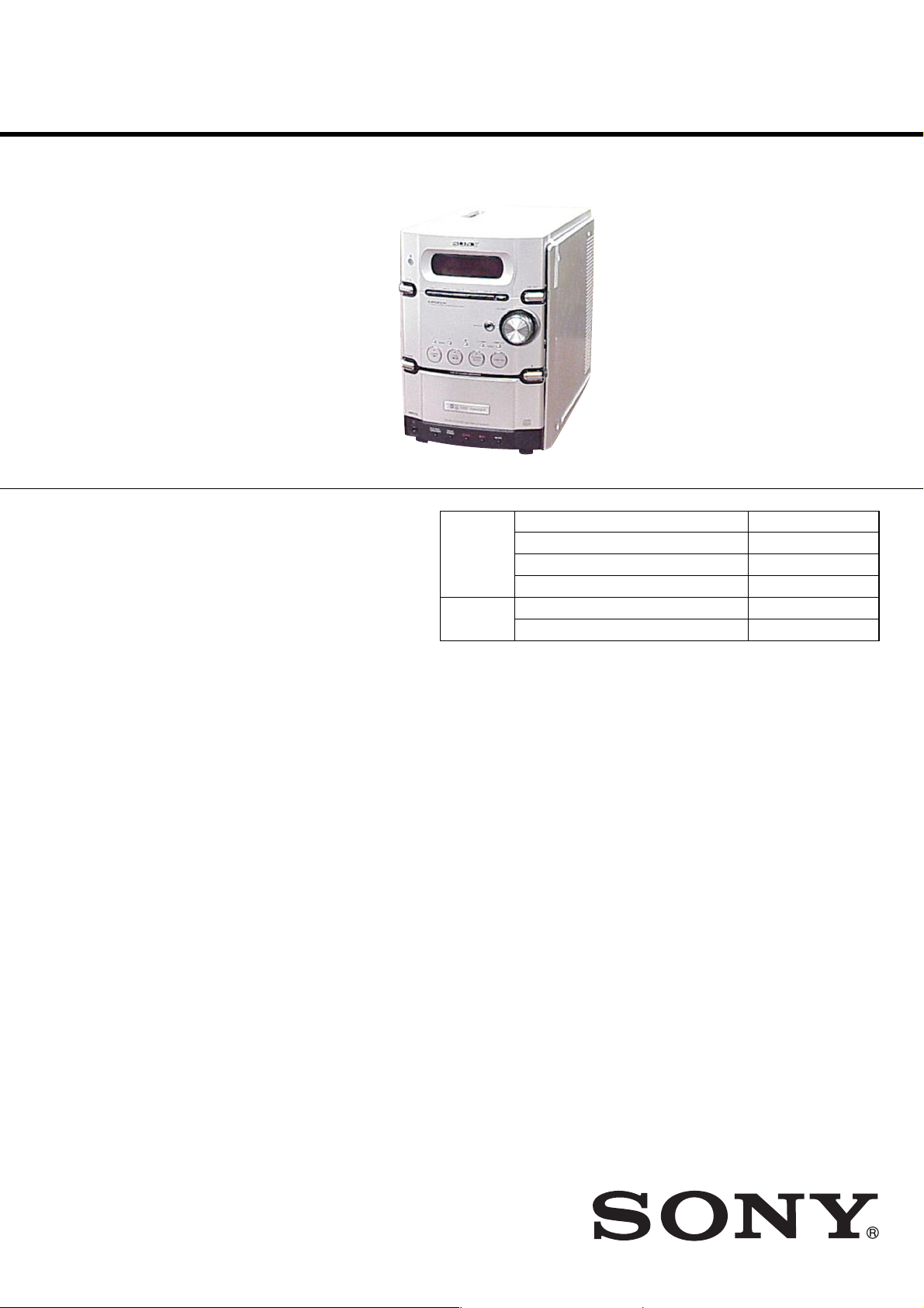
HCD-HPX10W
SERVICE MANUAL
Ver 1.0 2004.06
HCD-HPX10W is the amplifier, CD player,
tape deck and tuner section in CMT -HPX10W .
CD CD Mechanism Type CDM82A-F1BD81
Section Base Unit Name BU-F1BD81A
Tape deck Model Name Using Similar Mechanism HCD-HPX9
Section T ape Transport Mechanism Type CMAL5Z225A
US Model
Canadian Model
Model Name Using Similar Mechanism HCD-HPX9
Optical Pick-up Block Name KSM-215DCP
Main unit
Am
plifier section
For the United States model
AUDIO POWER SPECIFICATIONS
POWER OUTPUT AND TOTAL HARMONIC
DISTORTION:
With 6-ohm loads, both channels driven, from
120 – 10,000 Hz: rated 55 watts per channel
minimum RMS power, with no more than 10%
total harmonic distortion from 250 milliwatts to
rated output.
DIN power output (rated): 50 + 50 W
Continuous RMS power output (reference):
Music power output (reference): 100 + 100 W
Inputs
MD/VIDEO: Sensitivity 450/250 mV,
Outputs
PHONES: Accepts headphones with
(6 ohms at 1 kHz, DIN)
60 + 60 W
(6 ohms at 1 kHz, 10%
THD)
impedance 47 kilohms
an impedance of 8 ohms or
more.
SPECIFICATIONS
SPEAKER: o Accepts impedance of 6 t
CD player section
Laser
Frequency response
Tape deck section
Recording system
Frequency response
Tuner section
FM stereo, FM/AM superheterodyne tuner
FM tuner section
Tuning range
Antenna
Antenna terminals
ntermediate frequency
I
16 ohms.
Semiconductor laser
(λ=780 nm)
Emission duration:
continuous
20 Hz – 20 kHz
4-track 2-channel, stereo
50 – 13,000 Hz (±3 dB),
using Sony TYPE I
cassettes
87.5 – 108.0 MHz
FM lead antenna
75 ohms unbalanced
10.7 MHz
AM tuner section
Tuning range 530 – 1,710 kHz
(with the tuning interval
set at 10 kHz)
531 – 1,710 kHz
(with the tuning interval
set at 9 kHz)
Antenna AM loop antenna, external
antenna terminal
Intermediate frequency 450 kHz
General
Power requirements 120 V AC, 60 Hz
Power consumption 110 W
Design and specifications are subject to change
without notice.
9-877-914-01
2004F1678-1
© 2004.06
COMPACT DISC DECK RECEIVER
Sony Corporation
Home Audio Company
Published by Sony Engineering Corporation
Page 2

HCD-HPX10W
TABLE OF CONTENTS
1. SERVICING NOTES ................................................ 4
2. GENERAL ................................................................... 5
3. DISASSEMBLY
3-1. Disassembly Flow-1 ........................................................ 7
3-2. Disassembly Flow-2 ........................................................ 8
3-3. Optical Pick-Up Block .................................................... 9
3-4. Side Plate (L) (R), Top Panel Section.............................. 10
3-5. Mechanical Deck ............................................................. 11
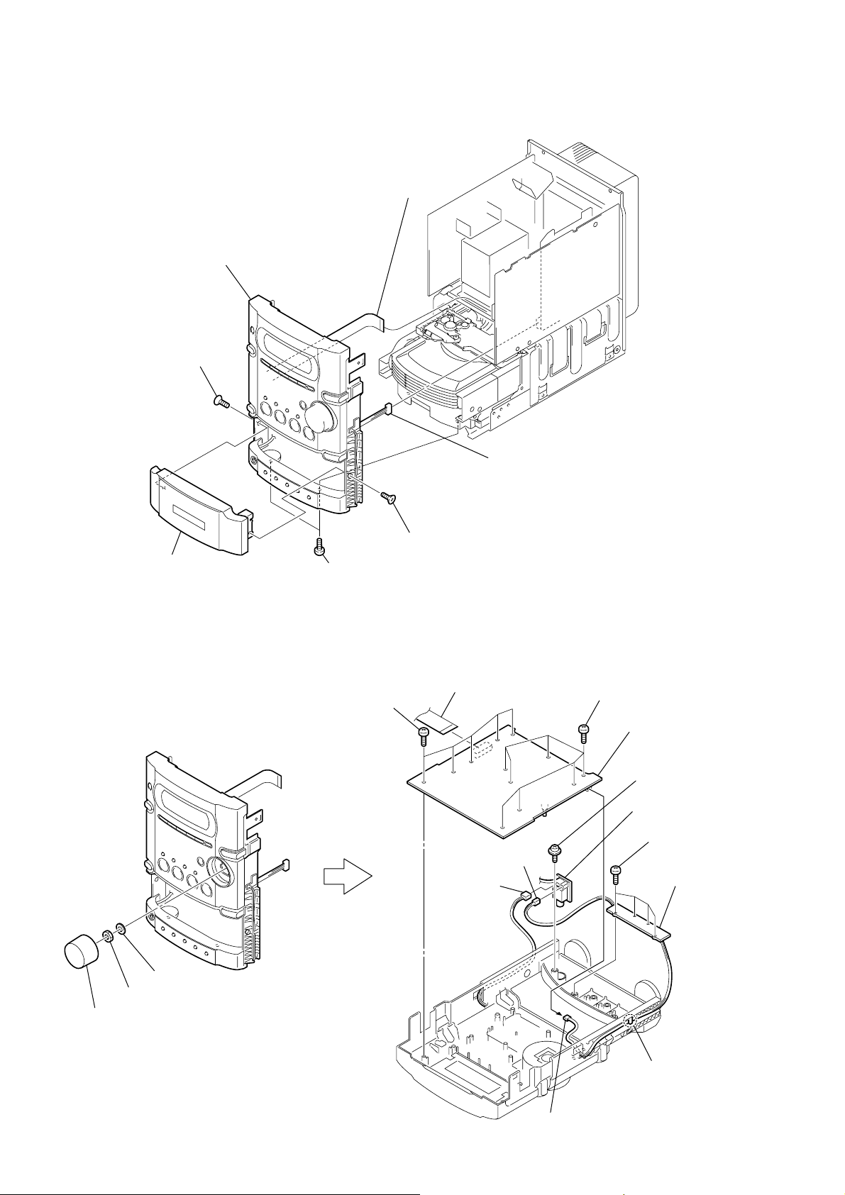
3-6. Front Panel Section ......................................................... 12
3-7. PANEL (1), (2) Board, HEADPHONE Board ................ 12
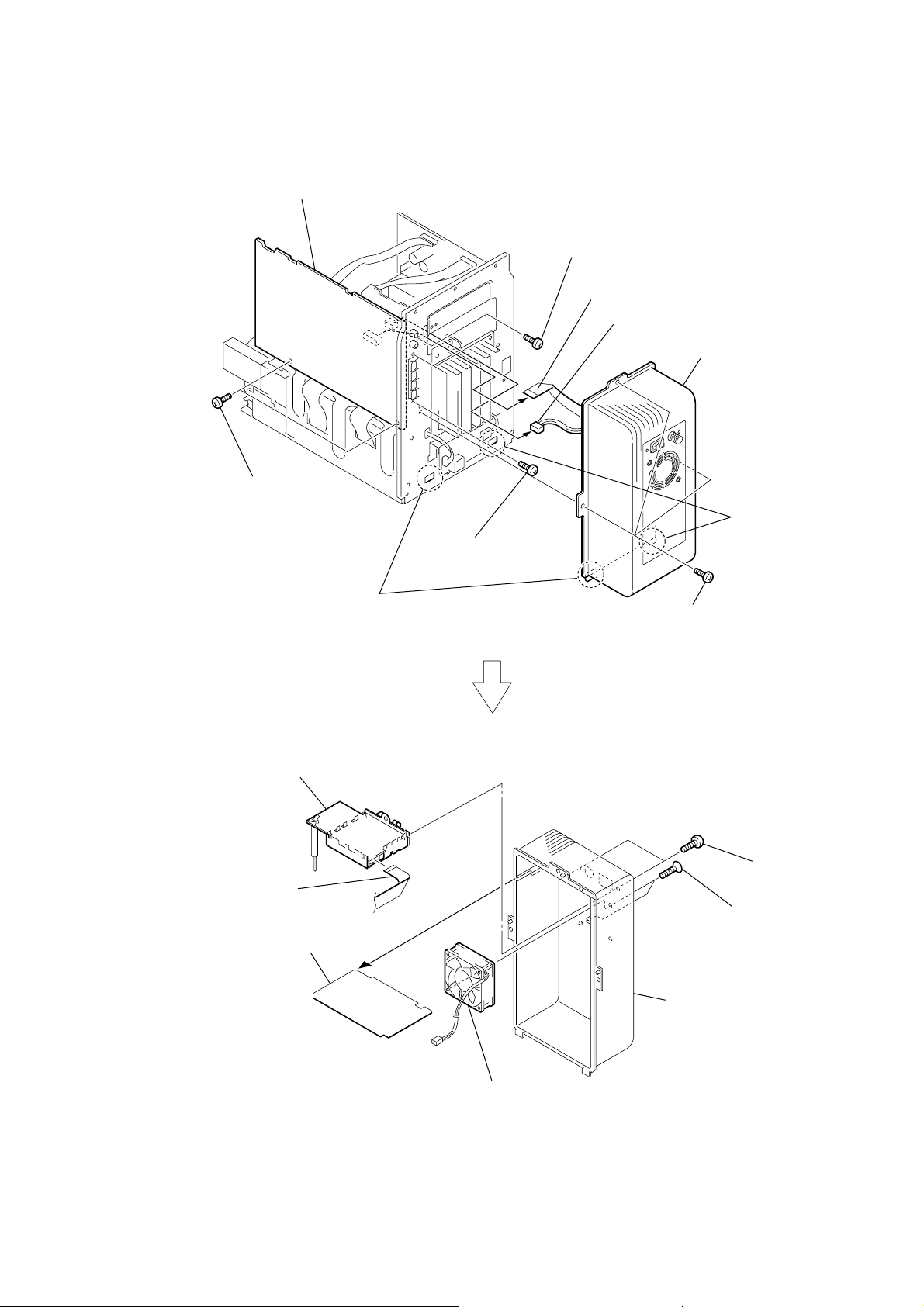
3-8. Tuner (FM/AM), DC Fan ................................................ 13
3-9. MAIN Board.................................................................... 14
3-10. Rear Panel Section........................................................... 14
3-11. AMP Board, Switching Regulator................................... 15
3-12. POWER Board ................................................................ 15
3-13. CD Mechanism Deck (CDM82A)................................... 16
3-14. Plate (Cover Top)............................................................. 17
3-15. Top Section ...................................................................... 17
3-16. Arm Section..................................................................... 18
3-17. CD Mechanism Deck Section ......................................... 19
3-18. Sub Gear (2 Step), Sub Slider Assy................................. 20
3-19. Arm (R) ........................................................................... 21
3-20. Gear (Stock Planet) (Right) ............................................. 22
3-21. Lever (Sub Gear Back L) ................................................ 22
3-22. Arm (L)............................................................................ 23
3-23. Gear (Stock Rot Long) (Left) .......................................... 24
3-24. Gear (Stock Rot Short) (Right) ....................................... 24
3-25. Stocker (1) Assy To Stocker (5) Assy.............................. 25
3-26. SPR-E (Roller Slider Upper) (Top Section) .................... 26
3-27. Rubber Roller (Top Section) ........................................... 26
3-28. LOD Motor...................................................................... 27
3-29. Slider (Push-popup)......................................................... 27
3-30. Rotary Encoder................................................................ 28
3-31. Assembling of the Rotary Encoder ................................. 29
3-32. ELV Motor....................................................................... 30
3-33. Chassis (Top), Chassis (Bottom) ..................................... 31
3-34. Lever (Loading R, Loading L) ........................................ 32
3-35. Disc Stop Lever ............................................................... 33
3-36. DRIVER Board ............................................................... 33
3-37. CD Board......................................................................... 34
3-38. Optical Pick-up (KSM-215DCP) .................................... 34
3-39. Base Unit Section ............................................................ 35
3-40. Lever (BU Lock) ............................................................. 35
3-41. Gear (IDL-B) ................................................................... 36
3-42. Gear (IDL-C) ................................................................... 36
3-43. SPR-E (Tako-Back) ......................................................... 37
3-44. Plate (Push) Assy............................................................. 38
3-45. SPR-P (Lock) .................................................................. 39
4. ASSEMBLY
4-1. Assembly Flow................................................................ 40
4-2. Assembling of the Stocker Section ................................. 41
4-3. Assembling of the Gear (Stock Rot Short) (Right) ......... 42
4-4. Assembling of the Gear (Stock Rot Long) (Left)............ 43
4-5. Confirming the Assembling of the Stocker Section ........ 44
4-6. Assembling of the Gear (Stock Rotary Left)................... 45
4-7. Assembling of the Gear (Stock Rotary Right) ................ 46
4-8. Assembling of the Lever (Sub Gear Back L) .................. 47
4-9. Assembling of the Gear (Sub Gear Pin Right) ................ 48
4-10. Assembling of the Lever (Sub Gear Back R).................. 49
4-11. Assembling of the Sub Gear (Idler) ................................ 50
4-12. Assembling of the Sub Gear (2 Step) .............................. 51
4-13. Confirming the Assembling of the Arm Section ............. 52
5. TEST MODE ............................................................... 53
6. ELECTRICAL ADJUSTMENTS .......................... 55
7. DIAGRAMS
7-1. Block Diagram – CD Servo Section –............................. 59
7-2. Block Diagram – MAIN Section –.................................. 60
7-3. Block Diagram
– PANEL/POWER SUPPLY Section – ........................... 61
7-4. Printed Wiring Board – CD Board – ............................... 62
7-5. Schematic Diagram – CD Board – .................................. 63
7-6. Printed Wiring Board – CD MECHANISM Section –.... 64
7-7. Schematic Diagram – CD MECHANISM Section – ...... 65
7-8. Printed Wiring Board – MAIN Board – .......................... 66
7-9. Schematic Diagram – MAIN Board (1/3) – .................... 67
7-10. Schematic Diagram – MAIN Board (2/3) – .................... 68
7-11. Schematic Diagram – MAIN Board (3/3) – .................... 69
7-12. Printed Wiring Board – AMP Board – ............................ 70
7-13. Schematic Diagram – AMP Board – ............................... 71
7-14. Printed Wiring Board – PANEL Section – ...................... 72
7-15. Schematic Diagram – PANEL Section – ......................... 73
7-16. Printed Wiring Board – POWER Board – ....................... 74
7-17. Schematic Diagram – POWER Board –.......................... 75
8. EXPLODED VIEWS
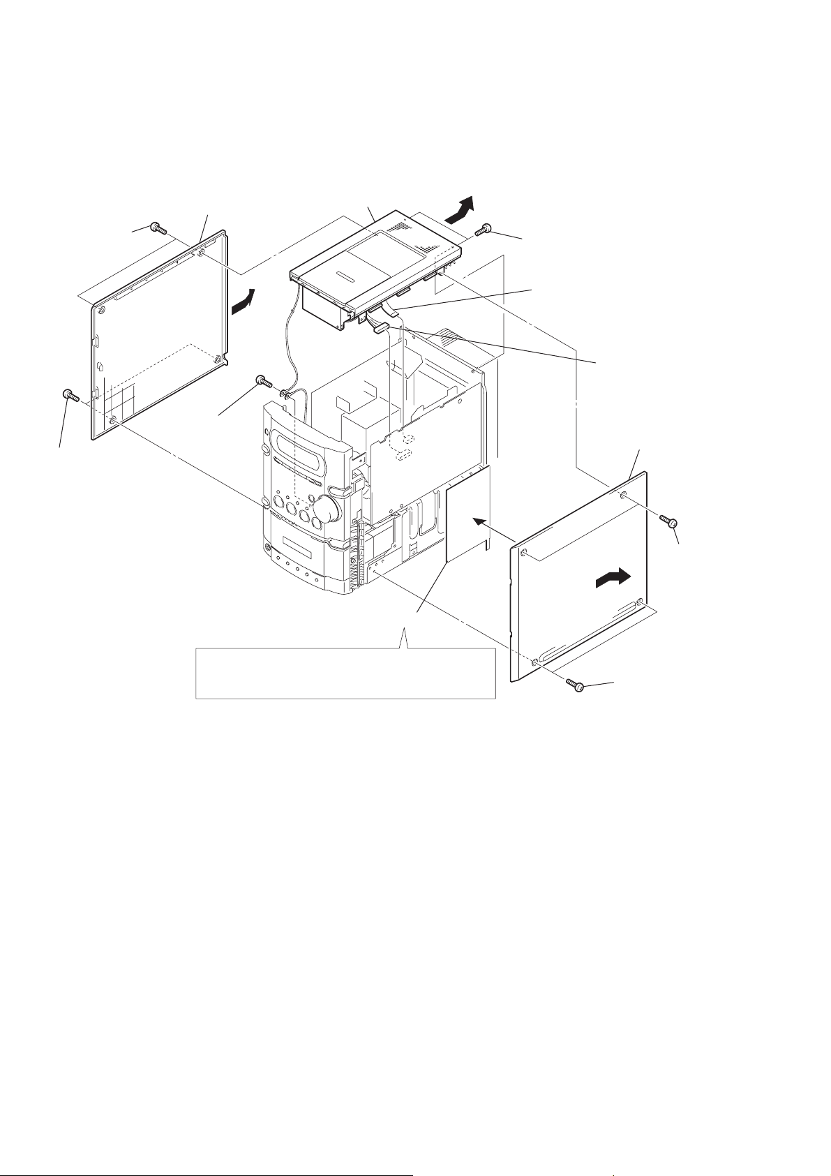
8-1. Side Plate, Top Panel Section .......................................... 83
8-2. Front Panel Section ......................................................... 84
8-3. Chassis Section................................................................ 85
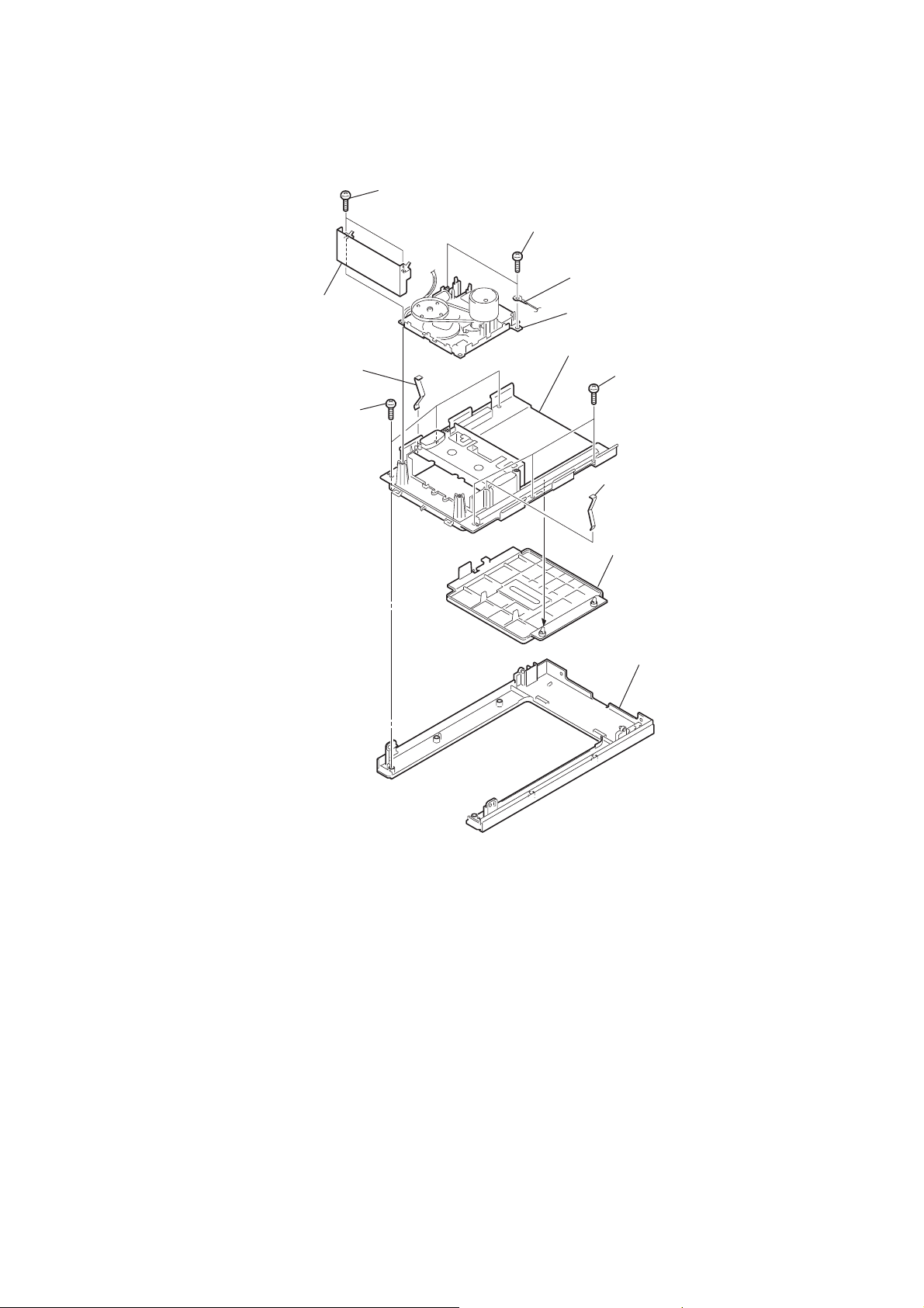
8-4. CD Mechanism Deck Section-1 (CDM82A) .................. 86
8-5. CD Mechanism Deck Section-2 (CDM82A) .................. 87
8-6. CD Mechanism Deck Section-3 (CDM82A) .................. 88
8-7. CD Mechanism Deck Section-4 (CDM82A) .................. 89
8-8. CD Mechanism Deck Section-5 (CDM82A) .................. 90
8-9. CD Mechanism Deck Section-6 (CDM82A) .................. 91
8-10. CD Mechanism Deck Section-7 (CDM82A) .................. 92
8-11. CD Mechanism Deck Section-8 (CDM82A) .................. 93
8-12. CD Mechanism Deck Section-9 (CDM82A) .................. 94
8-13. CD Mechanism Deck Section-10 (CDM82A) ................ 95
8-14. Base Unit Section (BU-F1BD81A) ................................. 96
9. ELECTRICAL PARTS LIST .................................. 97
2
Page 3
HCD-HPX10W
r
SAFETY CHECK-OUT
After correcting the original service problem, perform the following
safety check before releasing the set to the customer:
Check the antenna terminals, metal trim, “metallized” knobs, screws,
and all other exposed metal parts for AC leakage.
Check leakage as described below.
LEAKAGE TEST
The AC leakage from any exposed metal part to earth ground and
from all exposed metal parts to any exposed metal part having a
return to chassis, must not exceed 0.5 mA (500 microamperes.).
Leakage current can be measured by any one of three methods.
1. A commercial leakage tester, such as the Simpson 229 or RCA
WT -540A. Follow the manuf acturers’ instructions to use these
instruments.
2. A battery-operated A C milliammeter . The Data Precision 245
digital multimeter is suitable for this job.
3. Measuring the voltage drop across a resistor by means of a
VOM or battery-operated AC v oltmeter. The “limit” indication
is 0.75 V, so analog meters must have an accurate low-v oltage
scale. The Simpson 250 and Sanwa SH-63Trd are examples
of a passive VOM that is suitable. Nearly all battery operated
digital multimeters that have a 2 V A C range are suitable. (See
Fig. A)
To Exposed Metal
Parts on Set
Notes on chip component replacement
• Never reuse a disconnected chip component.
• Notice that the minus side of a tantalum capacitor may be
damaged by heat.
Flexible Circuit Board Repairing
• Keep the temperature of the soldering iron around 270 °C
during repairing.
• Do not touch the soldering iron on the same conductor of the
circuit board (within 3 times).
• Be careful not to apply force on the conductor when soldering
or unsoldering.
CAUTION
Use of controls or adjustments or performance of procedures
other than those specified herein may result in hazardous radiation
exposure.
This appliance is
classified as a CLASS 1
LASER product. This
label is located on the
rear exterior.
AC
0.15 µF
1.5 k
Ω
Earth Ground
voltmete
(0.75 V)
Fig. A. Using an AC voltmeter to check AC leakage.
SAFETY-RELATED COMPONENT WARNING!!
COMPONENTS IDENTIFIED BY MARK 0 OR DOTTED LINE
WITH MARK 0 ON THE SCHEMATIC DIAGRAMS AND IN
THE PARTS LIST ARE CRITICAL TO SAFE OPERATION.
REPLACE THESE COMPONENTS WITH SONY PARTS WHOSE
PART NUMBERS APPEAR AS SHOWN IN THIS MANUAL OR
IN SUPPLEMENTS PUBLISHED BY SONY.
ATTENTION AU COMPOSANT AYANT RAPPORT
LES COMPOSANTS IDENTIFIÉS PAR UNE MARQUE 0 SUR
LES DIAGRAMMES SCHÉMATIQUES ET LA LISTE DES
PIÈCES SONT CRITIQUES POUR LA SÉCURITÉ DE
FONCTIONNEMENT. NE REMPLACER CES COM- POSANTS
QUE PAR DES PIÈCES SONY DONT LES NUMÉROS SONT
DONNÉS DANS CE MANUEL OU D ANS LES SUPPLÉMENTS
PUBLIÉS PAR SONY.
À LA SÉCURITÉ!
UNLEADED SOLDER
Boards requiring use of unleaded solder are printed with the leadfree mark (LF) indicating the solder contains no lead.
(Caution: Some printed circuit boards may not come printed with
the lead free mark due to their particular size)
: LEAD FREE MARK
Unleaded solder has the following characteristics.
• Unleaded solder melts at a temperature about 40 °C higher
than ordinary solder.
Ordinary soldering irons can be used but the iron tip has to be
applied to the solder joint for a slightly longer time.
Soldering irons using a temperature regulator should be set to
about 350 °C.
Caution: The printed pattern (copper foil) may peel away if
the heated tip is applied for too long, so be careful!
• Strong viscosity
Unleaded solder is more viscou-s (sticky, less prone to flow)
than ordinary solder so use caution not to let solder bridges
occur such as on IC pins, etc.
• Usable with ordinary solder
It is best to use only unleaded solder but unleaded solder may
also be added to ordinary solder.
3
Page 4
HCD-HPX10W
SECTION 1
SERVICING NOTES
NOTES ON HANDLING THE OPTICAL PICK-UP
BLOCK OR BASE UNIT
The laser diode in the optical pick-up block may suffer electrostatic
break-down because of the potential difference generated by the
charged electrostatic load, etc. on clothing and the human body.
During repair, pay attention to electrostatic break-down and also
use the procedure in the printed matter which is included in the
repair parts.
The flexible board is easily damaged and should be handled with
care.
NOTES ON LASER DIODE EMISSION CHECK
The laser beam on this model is concentrated so as to be focused on
the disc reflective surface by the objective lens in the optical pickup block. Therefore, when checking the laser diode emission,
observe from more than 30 cm away from the objective lens.
LASER DIODE AND FOCUS SEARCH OPERATION
CHECK
Carry out the “S curve check” in “CD section adjustment” and check
that the S curve waveforms is output three times.
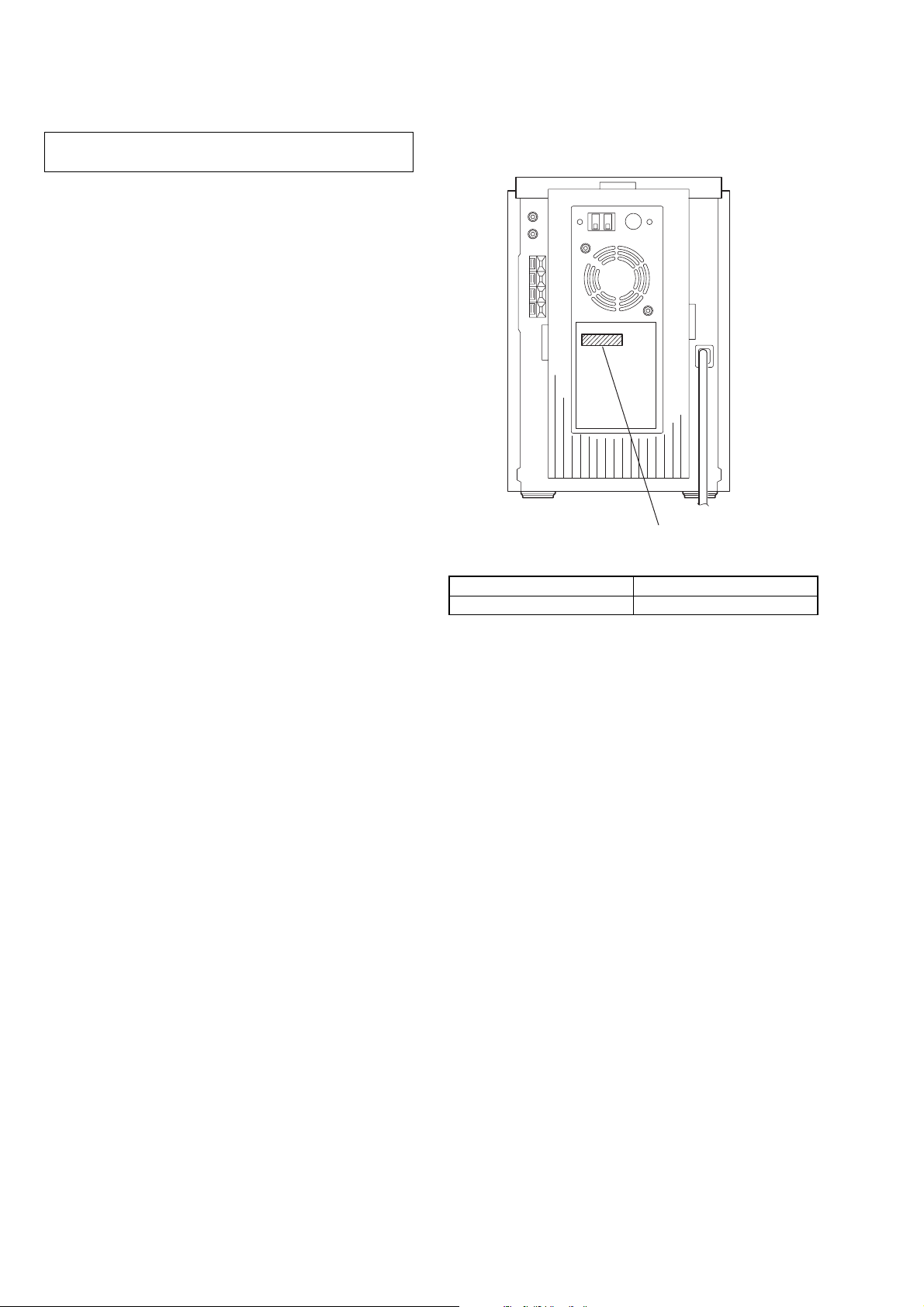
• MODEL IDENTIFICATION
– Rear View –
Power requirement
indication
Model Name Power Voltage Indication
US, Canadian models AC: 120 V - 60 Hz
4
Page 5
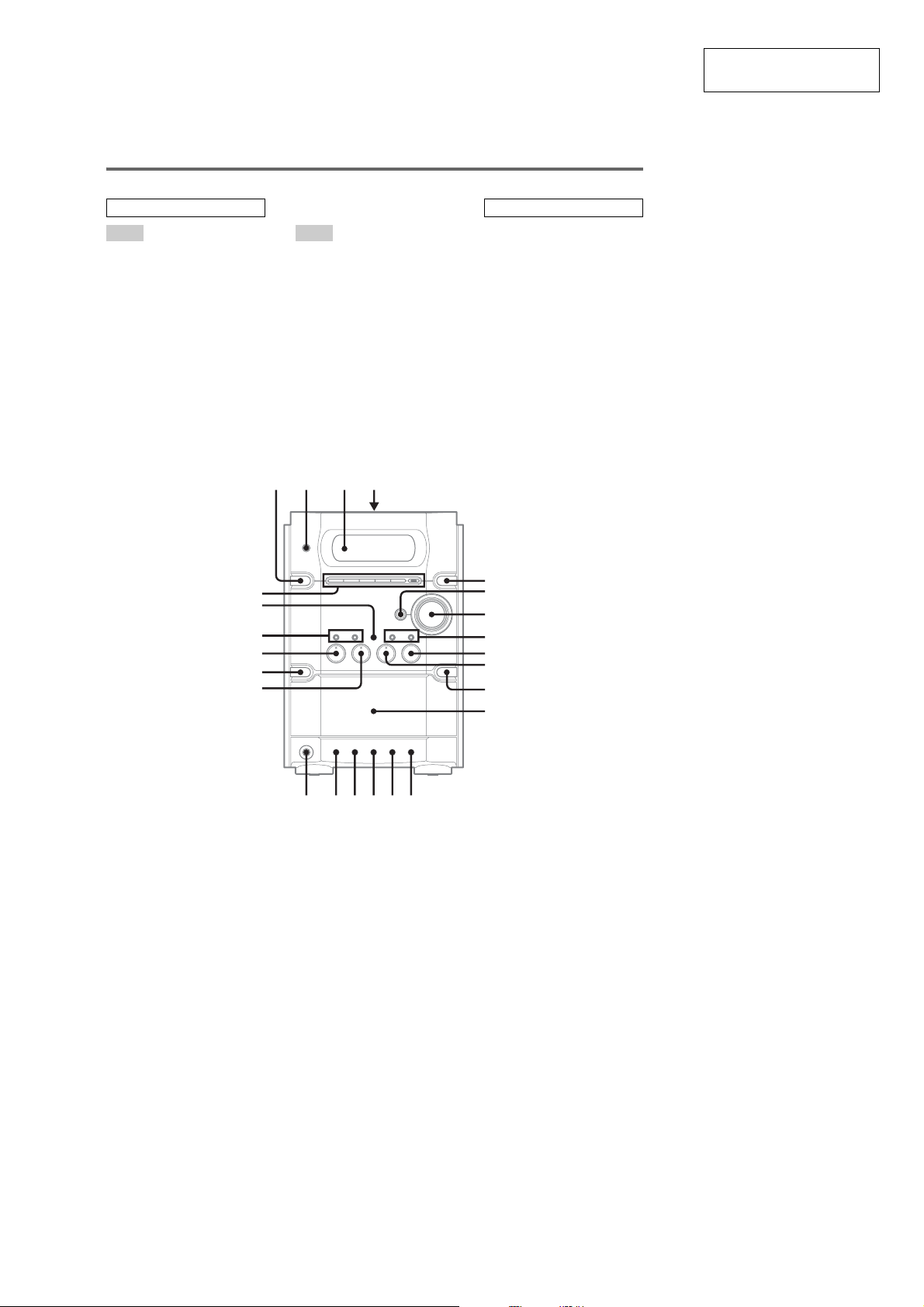
• LOCATION OF CONTROLS
Main unit
ALPHABETICAL ORDER
A – O P – Z
ALBUM +/– ws (11, 13)
Cassette compartment 4
CD SYNC qg (18)
DISC 1 – 5, +1 wf (11, 13)
DISC SKIP 5 (11, 13)
Disc tray qs (10)
Display window 3
DSGX 6 (19)
EX-CHANGE w; (10)
FM MODE qh (16, 27)
FUNCTION 9 (11, 13, 15, 17,
23)
PHONES jack qk
PLAY MODE qj (11, 13, 18)
Remote sensor 2
REPEAT qh (12)
TUNER/BAND 0 (14, 15)
TUNING +/– 8 (14, 15)
TUNING MODE qj (14, 15)
VOLUME 7 (20, 26)
12 34
SECTION 2
GENERAL
BUTTON DESCRIPTIONS
?/1 (power) 1 (8, 15, 20, 21,
28)
.m/M> (skip back/
skip forward, rewind/fast
forward) 8 (11, 13)
x wd (11, 15, 28)
X TAPE (pause) qd (17)
z REC qf (18)
CD/NX (play/pause) ql (11,
13, 27)
TAPE/N (play) wa (17)
Z (CD eject) qa (10, 11)
HCD-HPX10W
This section is extracted
from instruction manual.
wf
wd
ws
wa
w;
ql
+/1
5
6
7
x
lj JL
HS
8
9
A
0
qa
qs
zX
qf
qdqhqjqk qg
5
Page 6
HCD-HPX10W
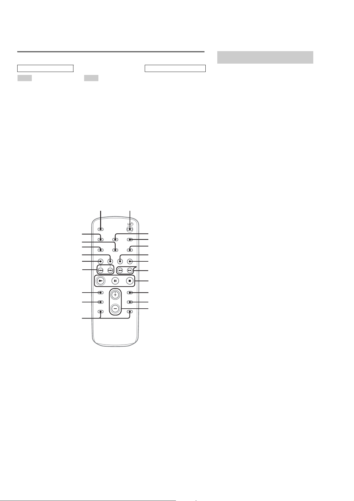
Remote control
ALPHABETICAL ORDER
A – O
ALBUM +/– qs (11, 13)
CD qj (11, 13, 15)
CLEAR qf (13)
CLOCK/TIMER SELECT 2
(20, 21, 26)
CLOCK/TIMER SET 3 (9, 20,
21)
DISC SKIP 0 (11, 13)
DISPLAY w; (16, 22)
ENTER 9 (9, 13, 20, 21)
EQ qd (19)
FM MODE 4 (16, 27)
FUNCTION 6 (11, 13, 15, 17,
23)
P – Z
PLAY MODE ql (11, 13, 18)
REPEAT 4 (12)
SLEEP wa (19)
TAPE qh (17)
TUNER/BAND 5 (14, 15)
TUNER MEMORY qk (14)
TUNING MODE ql (14, 15)
VOLUME +/– qa (20, 26)
wa 1
BUTTON DESCRIPTIONS
?/1 (power) 1 (8, 15, 20, 21,
28)
m/M (rewind/fast forward)
7 (11, 17)
./> (skip back/skip
forward) qg (9, 11, 13, 19, 20,
21)
x (stop) 8 (11, 15, 17, 18, 28)
X (pause) 8 (11, 17)
N (play) 8 (11, 13, 17, 27)
+/– (tuning) qg (14, 15)
Setting the clock
Use buttons on the remote for the operation.
1 Press ?/1 to turn on the system.
2 Press CLOCK/TIMER SET.
3 Press ./> repeatedly to set the
hour.
4 Press ENTER.
5 Press ./> repeatedly to set the
minute.
6 Press ENTER.
The clock starts working.
To adjust the clock
1 Press CLOCK/TIMER SET.
2 Press ./> until “CLOCK SET”
appears, then press ENTER.
3 Do the same procedures as step 3 to 6
above.
Note
The clock is not displayed in Power Saving Mode
w;
ql
qk
qj
qh
qg
qf
qd
qs
2
3
4
5
6
7
8
9
0
qa
6
Page 7
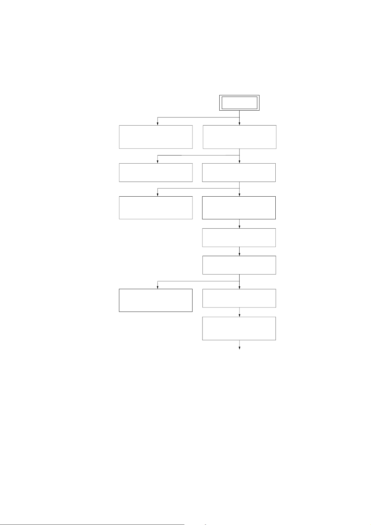
SECTION 3
DISASSEMBLY
•This is can be disassemble according to the following sequence.
3-1. DISASSEMBLY FLOW-1
HCD-HPX10W
SET
3-3.OPTICAL PICK-UP
BLOCK
(Page 9)
3-5.MECHANICAL DECK
(Page 11)
3-7.PANEL (1), (2) BOARD
HEADPHONE BOARD
(Page 12)
3-11.AMP BOARD,
SWITCHING REGULATOR
(Page 15)
3-4.SIDE PLATE (L) (R),
TOP PANEL SECTION
(Page 10)
3-6.FRONT PANEL SECTION
(Page 12)
3-8.TUNER (FM/AM),
DC FAN
(Page 13)
3-9.MAIN BOARD
(Page 14)
3-10.REAR PANEL SECTION
(Page 14)
3-12.POWER BOARD
(Page 15)
3-13.CD MECHANISM DECK
(CDM82A)
(Page 16)
to DISASSEMBLY FLOW-2
7
Page 8
HCD-HPX10W
3-2. DISASSEMBLY FLOW-2
from DISASSEMBLY FLOW-1
3-14. PLATE (COVER TOP)
(Page 17)
3-15. T OP SECTION
(Page 17)
3-16. ARM SECTION
(Page 18)
3-17. CD MECHANISM DECK
SECTION (Page 19)
3-26. SPR-E (ROLLER SLIDER UPPER)
(TOP SECTION) (Page 26)
3-18. SUB GEAR (2 STEP),
SUB SLIDER ASSY (Page 20)
3-19. ARM (R)
(Page 21)
3-20. GEAR (STOCK PLANET)
(RIGHT) (Page 22)
3-21. LEVER (SUB GEAR BACK L)
(Page 22)
3-22. ARM (L)
(Page 23)
3-23. GEAR (STOCK ROT LONG)
(LEFT) (Page 24)
3-24. GEAR (STOCK ROT SHORT)
(RIGHT) (Page 24)
3-25. STOCKER (1) ASSY TO
STOCKER (5) ASSY (Page 25)
3-27. RUBBER ROLLER
(TOP SECTION) (Page 26)
3-28. LOD MOTOR
(Page 27)
3-33. CHASSIS (TOP),
CHASSIS (BOTTOM) (Page 31)
3-34. LEVER
(LOADING R, LOADING L) (Page 32)
3-35. DISC STOP LEVER
(Page 33)
3-36. DRIVER BOARD
(Page 33)
8
3-29. SLIDER (PUSH-POPUP)
(Page 27)
3-37. CD BOARD (A)
(Page 34)
3-38. OPTICAL PICK-UP
(KSM-215DCP) (Page 34)
3-30. ROTARY ENCODER
(Page 28)
3-31. ASSEMBLING OF THE
ROTARY ENCODER (Page 29)
3-39. BASE UNIT SECTION
(Page 35)
3-40. LEVER (BU LOCK)
(Page 35)
3-41. GEAR (IDL-B)
(Page 36)
3-42. GEAR (IDL-C)
(Page 36)
3-32. ELV MOTOR
(Page 30)
3-43. SPR-E (TAKO-BACK)
(Page 37)
3-44. PLATE (PUSH) ASSY
(Page 38)
3-45. SPR-P (LOCK)
(Page 39)
Page 9
k
Note: Follow the disassembly procedure in the numerical order given.
3-3. OPTICAL PICK-UP BLOCK
2
bottom cover plate
4
screw
(BTTP M2.6)
5
BU stopper
6
insulator spring (coil)
qf
insulator
7
screw
(BTTP M2.6)
8
BU stopper
9
insulator spring (coil)
qg
insulator
1
two screws
(BVTT3
0
flotaing screw
(+PTPWH M2.6)
qa
insulator spring (coil)
qh
qs
flotaing screw
(+PTPWH M2.6)
qd
insulator spring (coil)
qj
insulator
×
6
)
insulator
qk
optical pick-up bloc
HCD-HPX10W
3
w
27p(CN201)
ire (flat type)
9
Page 10
HCD-HPX10W
)
3-4. SIDE PLATE (L) (R), TOP PANEL SECTION
qs
top panel section
5
6
two screws
(BVTP3
two screws
(BVTP3
×
×
6
)
10
7
side plate (L)
)
qa
screw
(BVTP3
×
6
)
8
two screws
(BVTP3
9
w
ire (flat type)
7p(CN317)
×
8
)
0
connector
(CN301)
4
side plate (R) assy
3
shield cover
When you exchange Side plate (R) assy,
please remove Shield cover from old Side plate (R),
and attach in new Side plate (R).
2
two screws
(BVTT3
1
two screws
(BVTP3
×
×
10
6
)
10
Page 11
3-5. MECHANICAL DECK
)
7
cassette shield plate
0
leaf spring (cassette)
2
three screws
(BVTP2.6
×
8
)
6
two screws
(BVTP2.6
HCD-HPX10W
×
8
)
5
two screws
(BVTP2.6
×
8
earth wire
8
qa
cassette panel
)
mechanical deck
1
three screws
(BVTP2.6
9
leaf spring (cassette
×
8
)
4
cassette door
3
top panel
11
Page 12
HCD-HPX10W
3-6. FRONT PANEL SECTION
7
front panel section
2
screw
(KTP3
×
8
)
5
w
ire (flat type) 19p(CN310)
3
CD panel
4
two screws
(BVTT3
3-7. PANEL (1), (2) BOARD, HEADPHONE BOARD
4
five screws
(BVTP2.6
1
screw
×
6
)
6
17p(CN801)
×
8
)
(KTP3
×
8
w
ire (flat type)
qa
(CN312)
0
connector
(CN311)
6
connector
(CN604)
)
connector
5
seven screws
(BVTP2.6
8
×
8
)
PANEL (1) board
9
screw
(PWH2.6
qs
HEADPHONE board
qf
PANEL (2) board
qd
four screws
(BVTP2.6
×
10
)
×
8
)
1
12
knob
(volume)
2
nut
3
washer
7
connector
(CN802)
qg
claw
Page 13
3-8. TUNER (FM/AM), DC FAN
qf
two screws (FAN)
1
two screws
(BVTP3
×
8
)
2
screw
(BVTP3
×
8
)
3
two screws
(BVTP3
×
8
)
4
three screws
(BVTP3
×
8
)
0
two screws
(BVTP3
×
10
)
8
connector
(CN313)
6
claw
qg
DC fan
qa
tuner (FM/AM)
qd
heat cover plate
5
claw
9
w
ire (flat type) 11p or 15p(CN305)
qs
w
ire (flat type) 11p or 15p
7
heat sink cover
heat sink cover
MAIN board
HCD-HPX10W
13
Page 14
HCD-HPX10W
)
3-9. MAIN BOARD
6
connector
(CN308)
5
connector
(CN303)
3
connector
(CN316)
2
connector
(CN307)
4
connector
(CN309)
3-10. REAR PANEL SECTION
1
w
ire (flat type)
(9p)(CN306)
7
w
ire (flat type)
(21p)(CN315)
4
(CN904)
8
w
ire (flat type)
(27p)(CN304)
connector
5
connector
(CN903)
9
MAIN board
6
connector
(CN602)
7
rear panel section
1
two screws
(BVTP3
×
8)
14
3
three screws
(BVTP3
2
two screws
(BVTP3
×
8
)
×
16
Page 15
3-11. AMP BOARD, SWITCHING REGULATOR
7
screw
(BVTP3
8
two screws
(BVTP3
9
AMP board
×
16
)
HCD-HPX10W
rear panel
×
8
)
5
two screws
(BVTP3
×
12
)
6
main heat sink
1
connector
(CN101)
3-12. POWER BOARD
3
two screws
(BVTT4
5
POWER board
×
6
)
1
connector
(CN901)
2
connector
(CN201)
2
connector
(CN902)
3
two screws
(BVTP3
4
SWITCHING REGULATOR
×
6
)
4
two screws
(BVTT4
×
6
)
15
Page 16
HCD-HPX10W
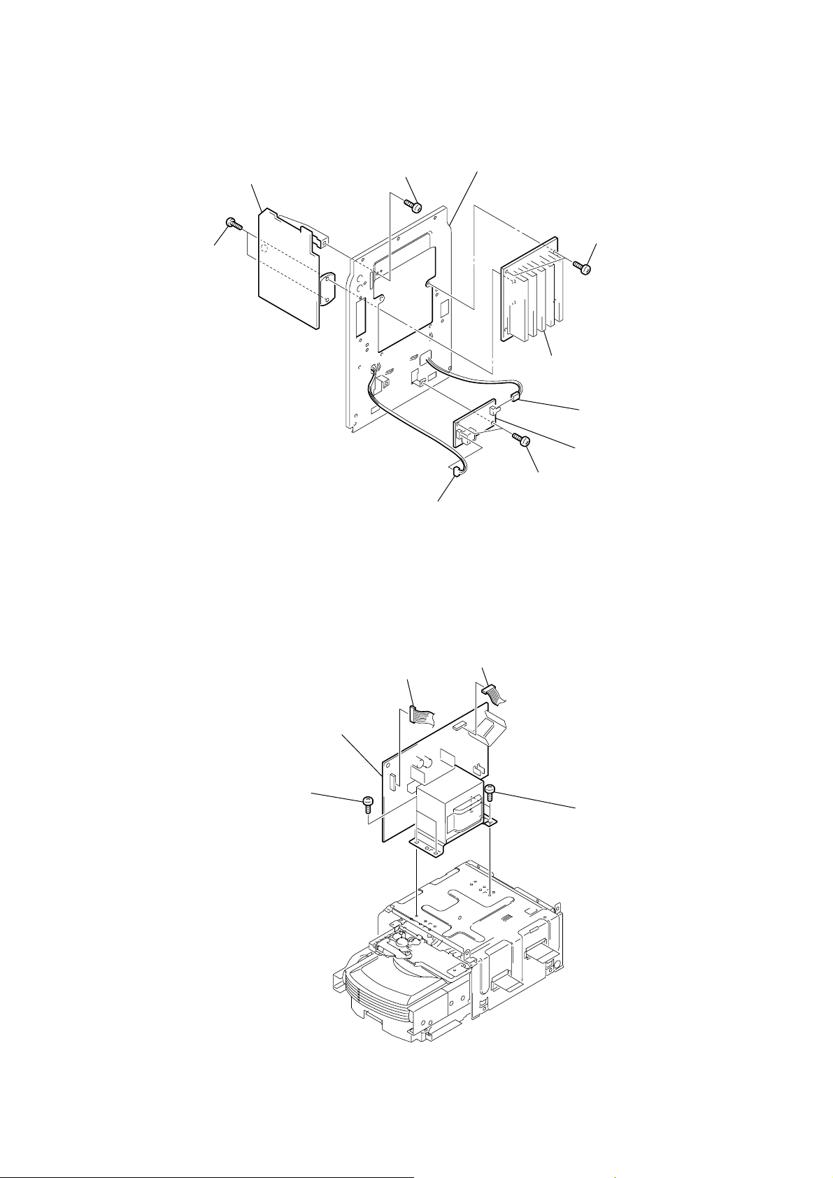
3-13. CD MECHANISM DECK (CDM82A)
1
two screws
(BVTT3
×
6
)
3
sub chassis
2
two screws
(BVTT3
×
6
8
plate
6
)
screw
(BVTP2.6
7
screw
(BVTT3
4
5
clamp
×
8
)
×
6
screw
(BVTP2.6
Please attach connector,
as shown in a figure.
plate
)
×
8
)
clamp
sub chassis
connector
qd
w
21p (CN202)
qa
w
ire (flat type)
27p (CN801)
ire (flat type)
9
four screws
(BVTT3
0
chassis
qs
×
10
)
ffc cover
qf
CD mechanism deck
(CDM82A)
16
Page 17
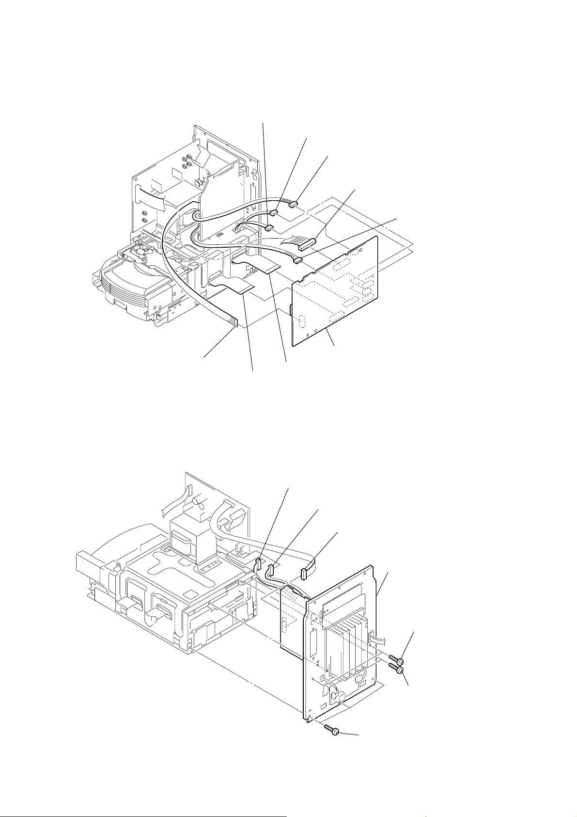
3-14. PLATE (COVER TOP)
)
2
gear (joint op), shaft (stock)
7
screw
(BTTPM 2.6
3
four screws
(BTTPM 2.6
8
plate (cam R)
×
8)
×
HCD-HPX10W
8)
4
plate (cover top)
3-15. TOP SECTION
3
two screws
×
(BTP 2
8)
shock guard
(lower)
1
screw (BTP 2
2
gear (connection tp)
×
8)
4
two screws
(PTPWH 2
7
top section
×
14)
1
gear (joint op)
6
plate (cam L)
5
screw
(BTTPM 2.6
6
shock guard
(lower)
5
claw
×
8
8
shaft (connection)
17
Page 18
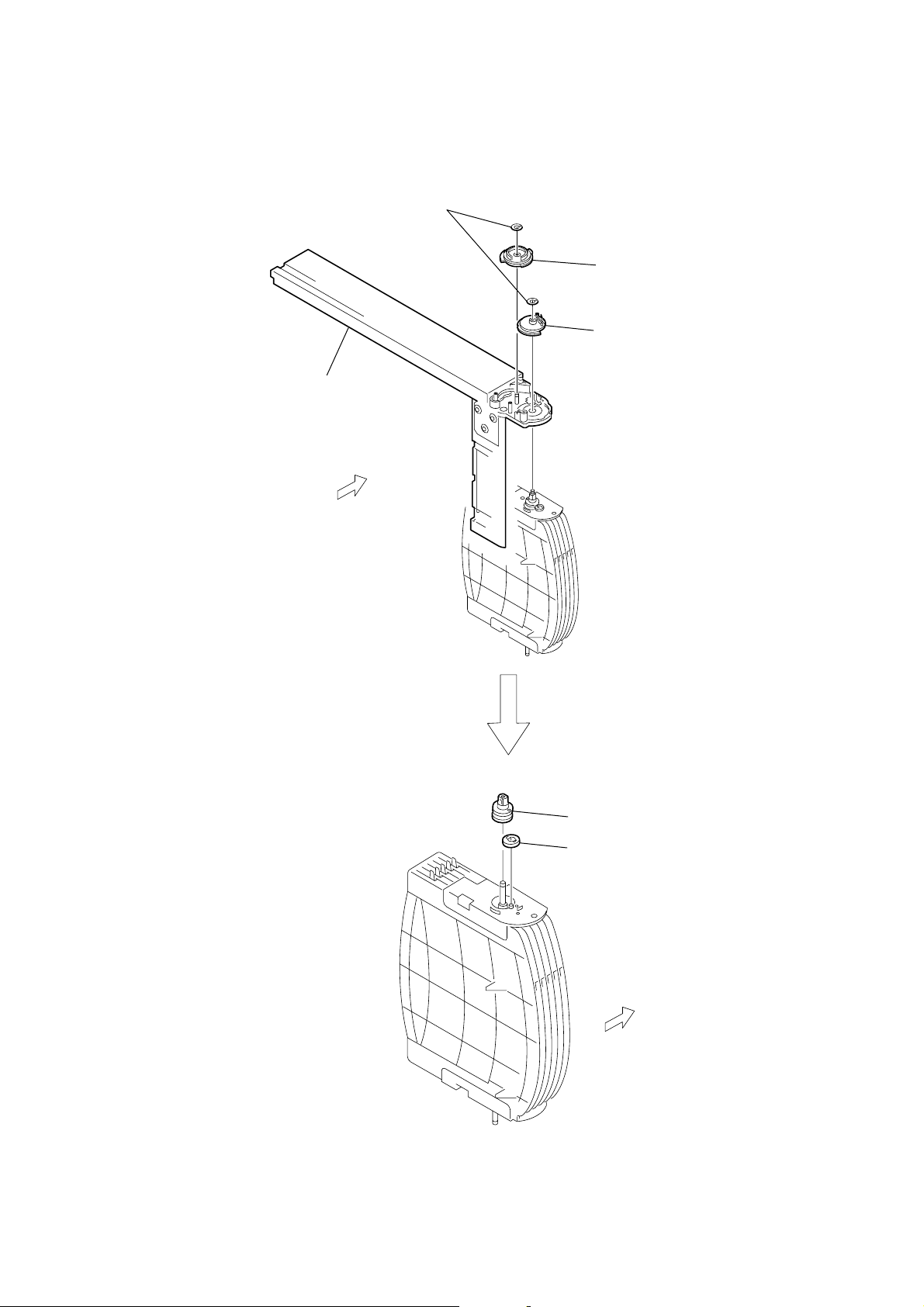
HCD-HPX10W
3-16. ARM SECTION
2
Slide the arm section in the
direction of the arrow B.
5
Remove the
in the direction of the arrow D.
arm section
3
claw
B
1
T
urn over the
in the direction of the arrow
PRECAUTION DURING ARM SECTION
INSTALLATION
pulley (LOD motor)
A
.
1
gear (joint op),
two shaft (shaft) stocks
A
D
6
arm section
C
4
Push this portion with a finger
in the direction of the arrow C.
3
turn over the
gear (swing)
in the direction
of the arrow.
6
Push this portion with a finger
in the direction of the arrow C.
gear (swing)
5
arm section
2
loosen two
screws
4
two claws
8
gear (joint op), two shaft (shaft) stocks
7
two
screws
18
Page 19
3-17. CD MECHANISM DECK SECTION
pulley (ELV motor)
A
HCD-HPX10W
2
Slide the
in the direction of the arrow
B
CD mechanism deck section
B
.
1
T
urn over the
in the direction of the arrow
pulley (ELV motor)
plate (cam L)
A
.
3
four
claws
4
Remove the CD mechanism deck section
in the direction of the arrow
C
C
.
19
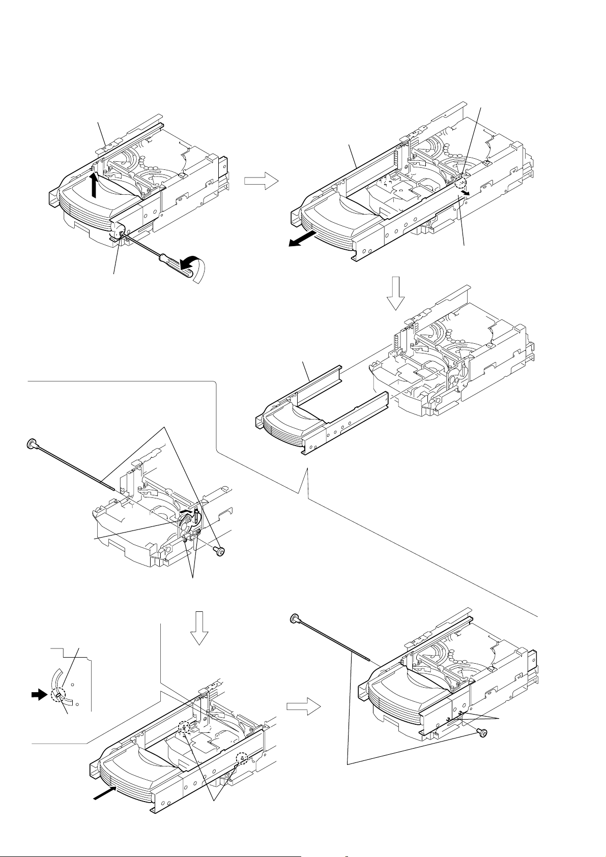
Page 20
HCD-HPX10W
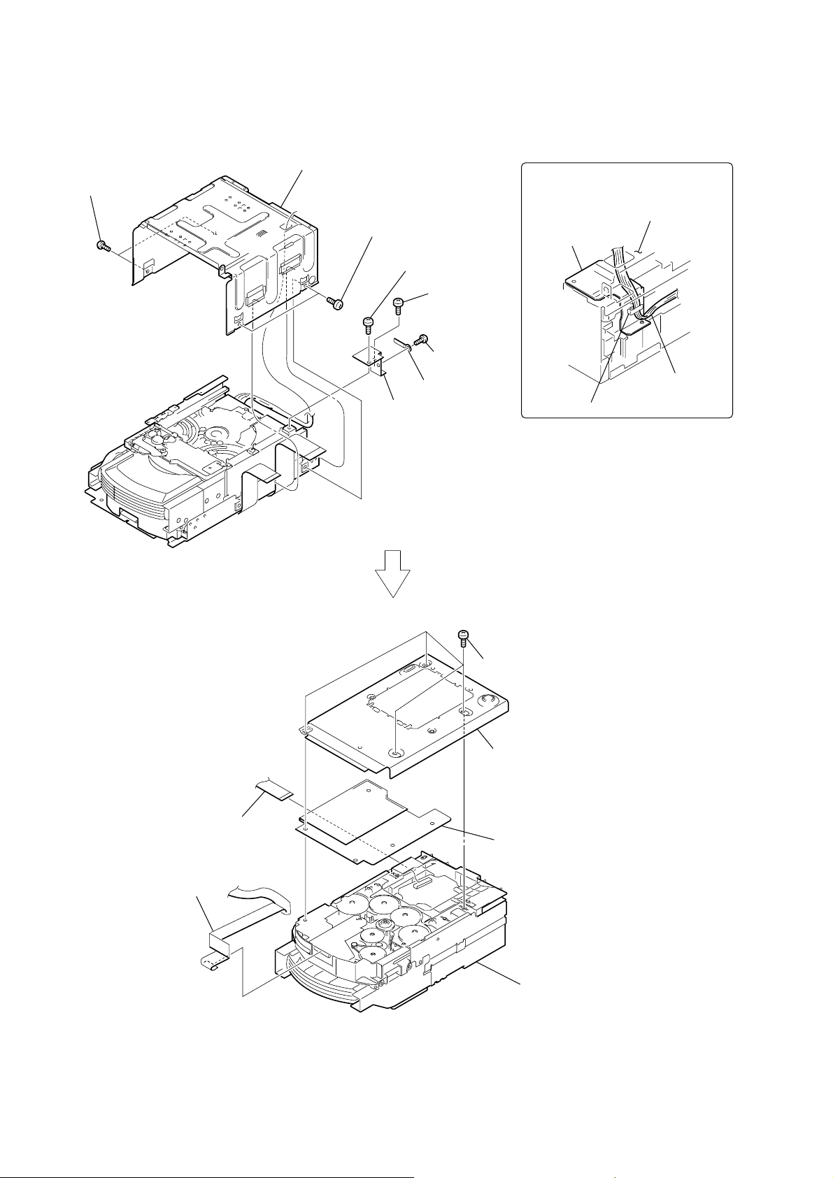
3-18. SUB GEAR (2 STEP), SUB SLIDER ASSY
9
Remove the
in the direction of the arrow.
sub slider assy
0
sub slider assy
5
sub gear (2 step)
sub slider assy
4
sub gear (idler)
1
k tapping screw (K2.6
3
2
two screws (M2
×
8)
cover (R)
×
5)
20
6
7
sub gear (idler)
8
sub gear (idler)
sub gear (idler)
Page 21
3-19. ARM (R)
)
3
lever (sub gear back R)
1
sub gear (joint just front)
2
SPR-T (sub gear back R)
HCD-HPX10W
7
gear (stock joint)
6
gear (stock rotary right)
5
gear (sub gear pin right
4
two washers (5.5)
9
arm (R)
8
two screws
× 5
(K2
)
21
Page 22
HCD-HPX10W
)
)
3-20. GEAR (STOCK PLANET) (RIGHT)
1
two screws (BTTP M2.6
2
stock base (A)
3
gear (stock sun)
4
gear (stock planet)
×
6
3-21. LEVER (SUB GEAR BACK L)
5
gear (stock joint),
shaft (stock)
UPPER
SIDE
2
screw (M2
1
3
6
7
lever (sub gear back L)
4
sub gear (joint just front)
×
5)
screw (K2.6
cover (L)
SPR-T (sub gear back L
×
8)
22
Page 23
3-22. ARM (L)
)
4
arm (L), stock base (B)
1
two washers (5.5)
UPPER
SIDE
HCD-HPX10W
2
gear (sub gear pin right
3
gear (stock rotary right)
6
gear (stock sun)
5
gear (stock planet)
UPPER
SIDE
23
Page 24
HCD-HPX10W
)
3-23. GEAR (STOCK ROT LONG) (LEFT)
2
stock box (L)
3
gear (stock rot short)
4
gear (stock rot long)
1
two screws (2
short
long
UPPER
SIDE
×
6)
3-24. GEAR (STOCK ROT SHORT) (RIGHT)
1
two screws (2
2
screw (1.7)
short
UPPER
SIDE
×
6)
3
stock box (R)
4
gear (stock rot short)
5
gear (stock rot short
24
Page 25
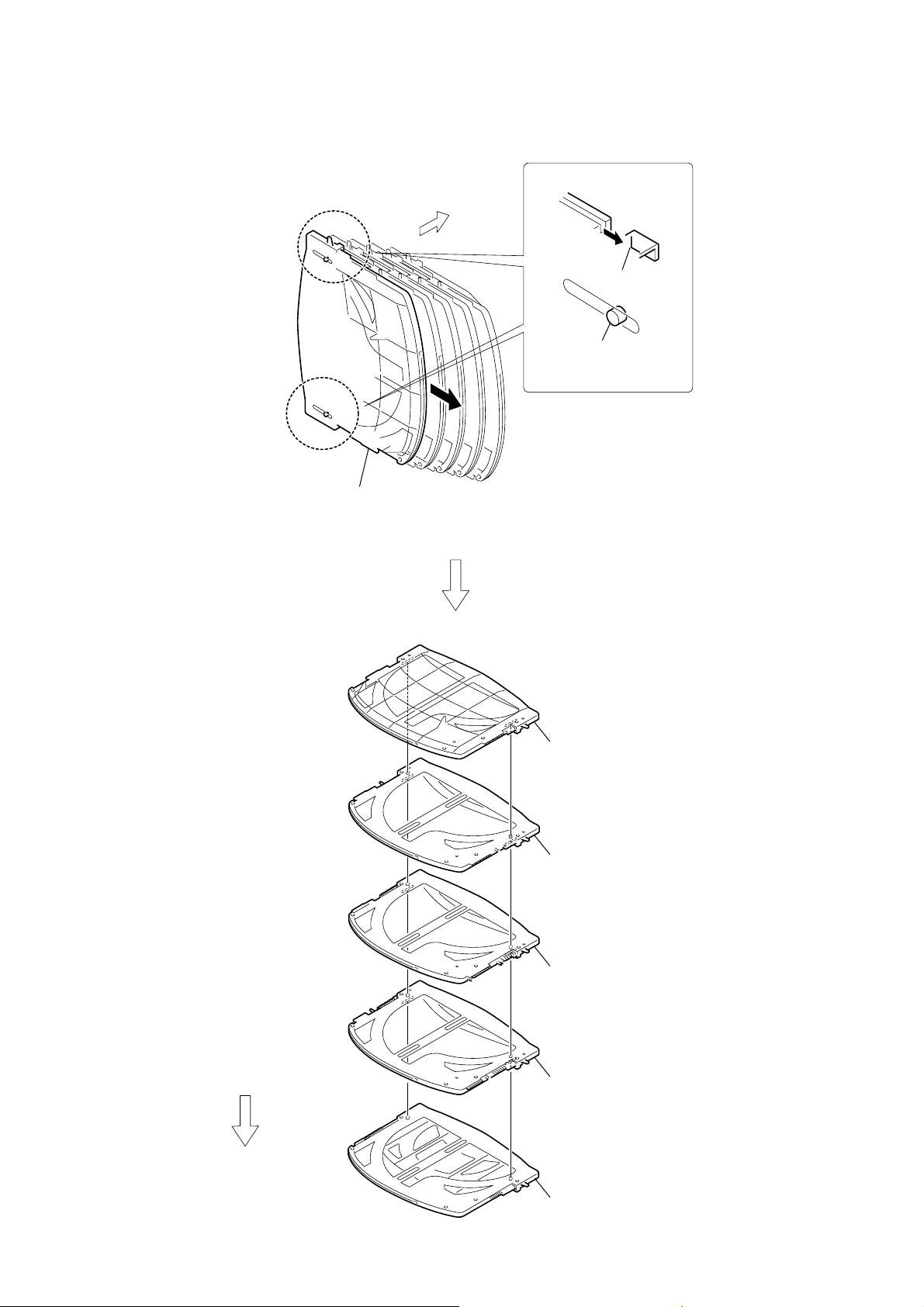
3-25. STOCKER (1) ASSY TO STOCKER (5) ASSY
UPPER
SIDE
1
dowel
2
claw
HCD-HPX10W
3
Remove the stocker
in the direction of the arrow.
(1) assy
Repeat the steps 1 to 1, when removing the part
(2), (3), (4) and (5) of the stocker assy.
4
stocker (1) assy
5
stocker (2) assy
UPPER
SIDE
6
stocker (3) assy
7
stocker (4) assy
8
stocker (5) assy
25
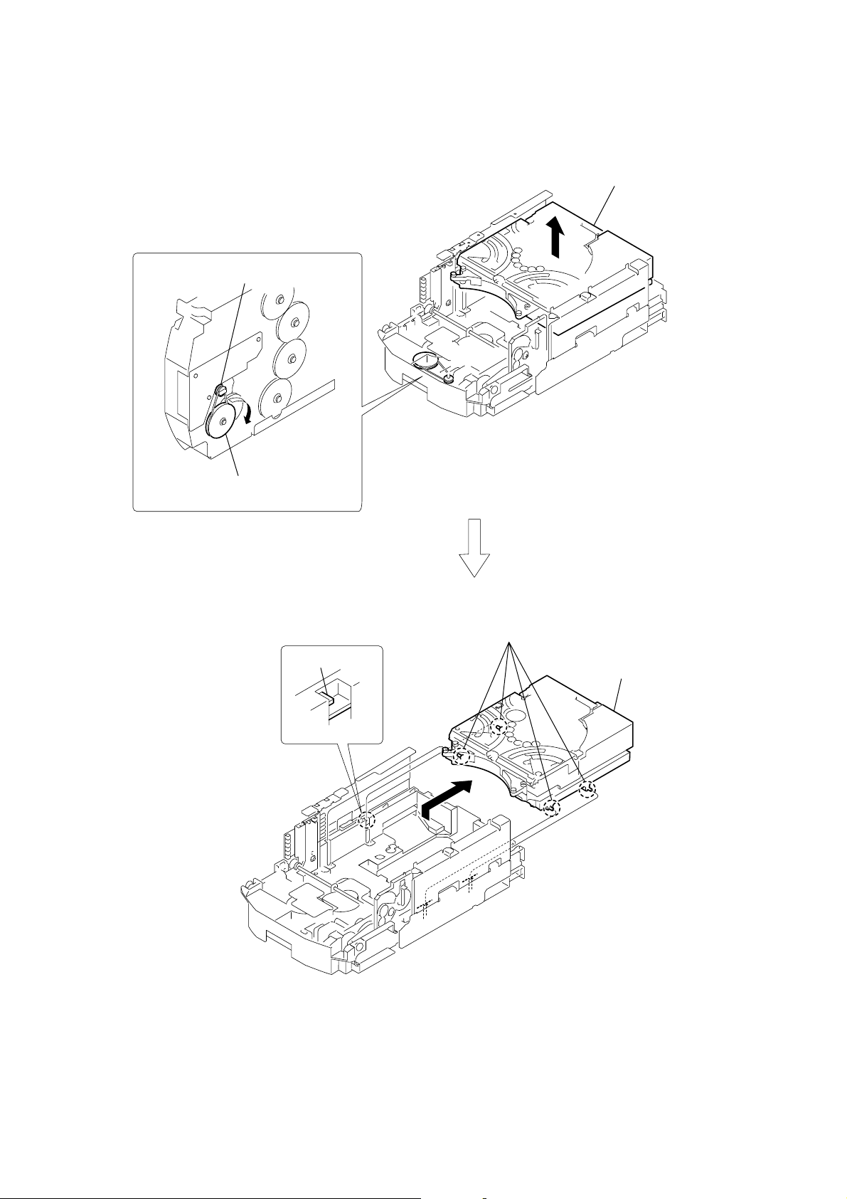
Page 26
HCD-HPX10W
3-26. SPR-E (ROLLER SLIDER UPPER) (TOP SECTION)
5
bushing
UPPER
SIDE
3
SPR-E (8 cm slider L)
1
bushing
2
SPR-T (8 cm slider R)
4
SPR-E
(roller slider upper)
3-27. RUBBER ROLLER (TOP SECTION)
4
two screws
(2
×
5)
5
two parasols
6
two
rubber rollers
1
two screws
(2
×
5)
2
two parasols
3
two
rubber rollers
top section
two claws
26
UPPER
SIDE
two claws
parasol
rubber roller
top section
Page 27
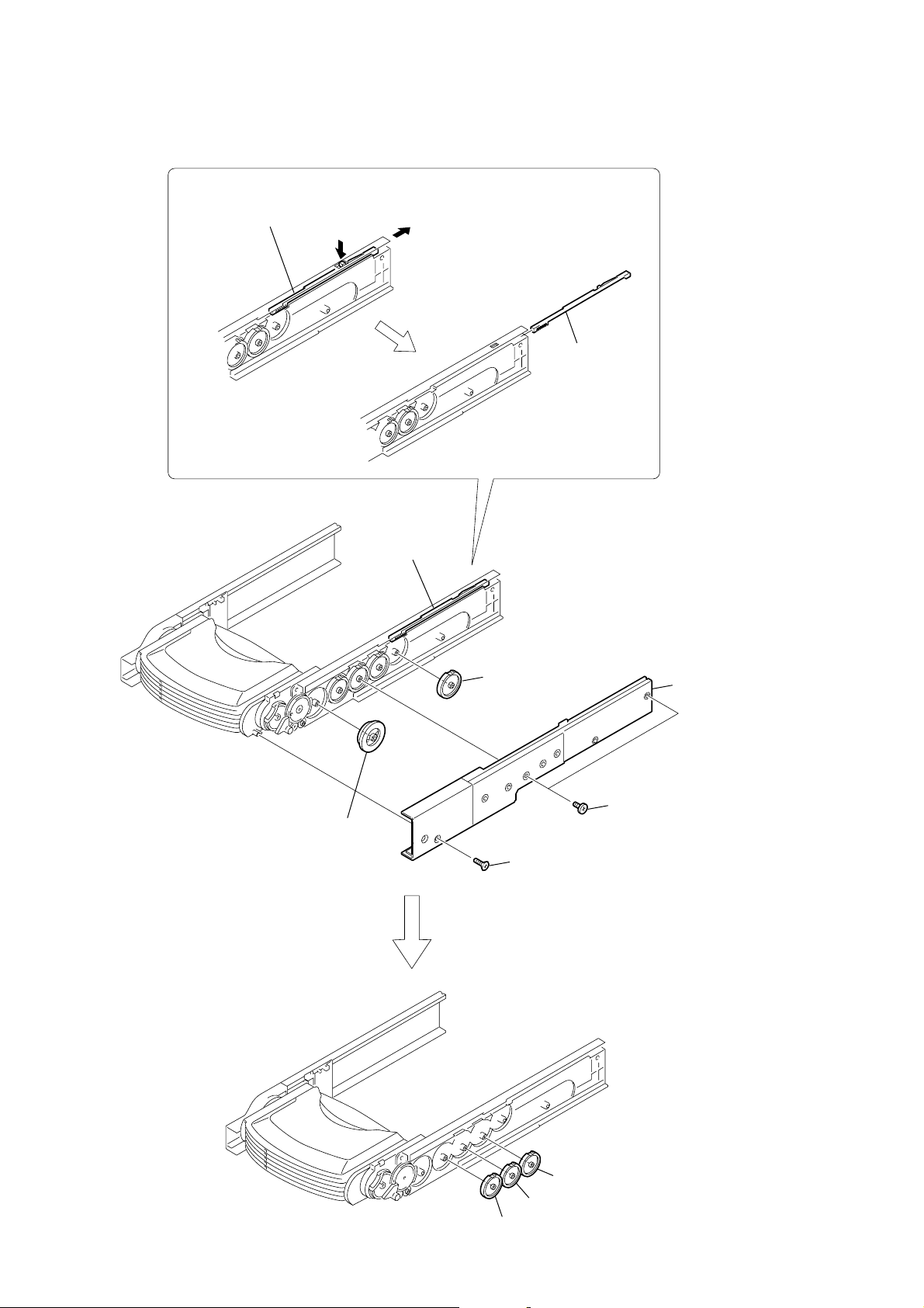
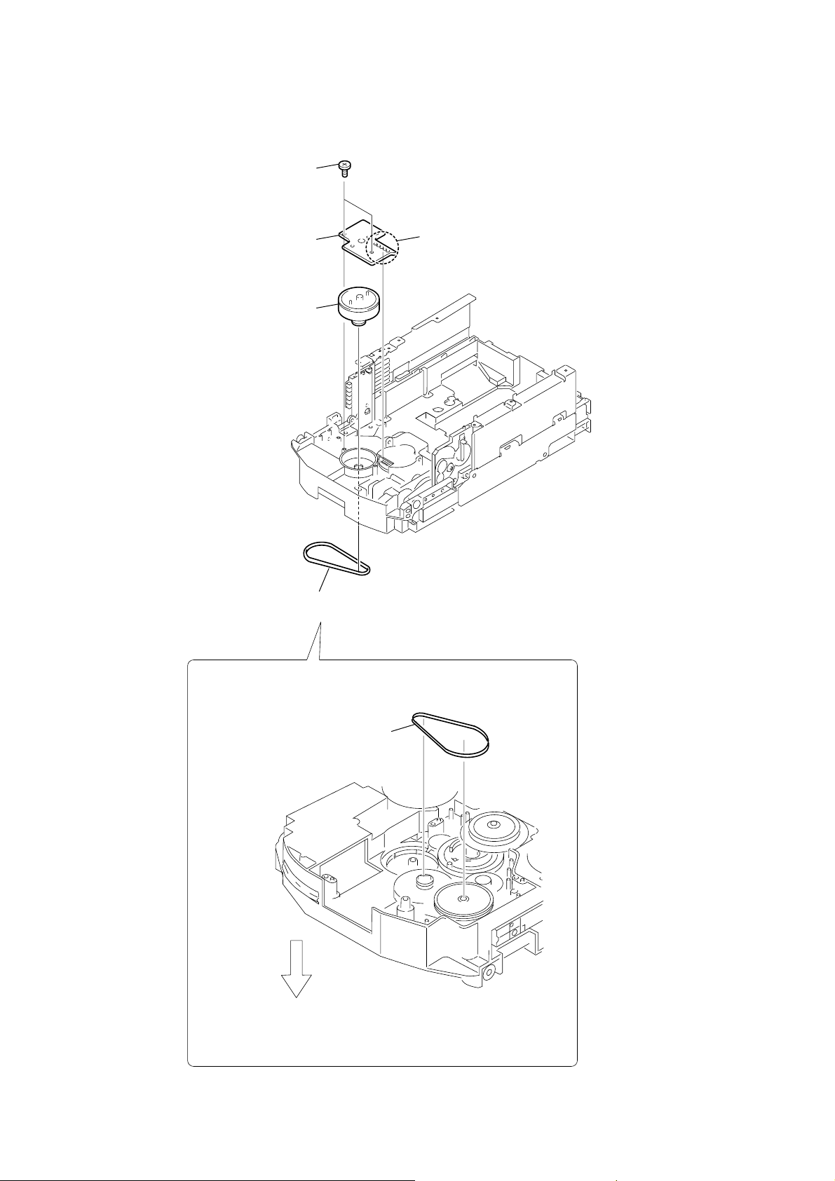
3-28. LOD MOTOR
)
3
claw
4
Remove the slider (push-popup1)
in the direction of the arrow.
2
sub chassis assy (R)
slider (push-popup 1)
slider (push-popup 2)
1
two screws
(BTTP M2.6
×
8)
2
sub chassis assy (L)
5
two screws
(BTTP M2.6
7
LOD MOTOR board
×
6
Remove soldering from the two points
3
8)
8
LOD motor
three screws
(BTTP M2.6
HCD-HPX10W
×
8)
4
belt (MOT-OP
3-29. SLIDER (PUSH-POPUP)
1
two screws
(BTTP M2.6
×
8)
27
Page 28
HCD-HPX10W
3-30. ROTARY ENCODER
4
Rotate the
the hole on the chassis can be seen
through the plate (comR).
ELV
motor until the position for
plate (com R)
1
three screws
(BTTP M2.6
×
6)
2
RELAY board
6
screw
(PTPWH2.6
8
screw
(PTPWH2.6
0
screw
(PTPWH2.6
qs
screw
(PTPWH2.6
qf
step tapping screw
(PWH2
×
×
6)
×
8)
3
Rotate the ELV motor in
the direction of the arrow.
×
8)
7
×
8)
8)
9
qa
gear (geneva 1)
qd
gear (encoder)
gear (pulley UD)
gear (geneva 2)
28
qg
Remove soldering
from the five points
qj
rotary encoder
qh
two claws
Page 29
3-31. ASSEMBLING OF THE ROTARY ENCODER
4
screw
(PTPWH2.6
2
two claws
3
Apply the soldering
in five points.
8
screw
(PTPWH2.6
gear (encoder)
5
gear (encoder)
×
HCD-HPX10W
8)
×
8)
1
rotary encoder
9
screw
(PTPWH2.6
6
gear (geneva 1)
×
8)
rotary encoder
qd
Align the plate (com R)
and the chassis hole.
7
gear (geneva 2)
gear (geneva 1)
gear
(geneva 1)
Adjust phases.
qa
Adjust phases.
qh
screw
(PTPWH2.6
qg
gear (pulley UD)
×
qs
screw
(PTPWH2.6
0
gear (geneva 2)
8)
×
8)
qf
Align the plate (com L)
and the chassis hole.
plate (com R)
plate (com L)
29
Page 30
HCD-HPX10W
3-32. ELV MOTOR
2
two screws
(BTTP M2.6
4
ELV MOTOR board
5
ELV
×
8)
motor
3
Remove soldering
from the five points
1
belt (MOT-UD)
belt (MOT-UD)
UPPER
SIDE
30
Page 31

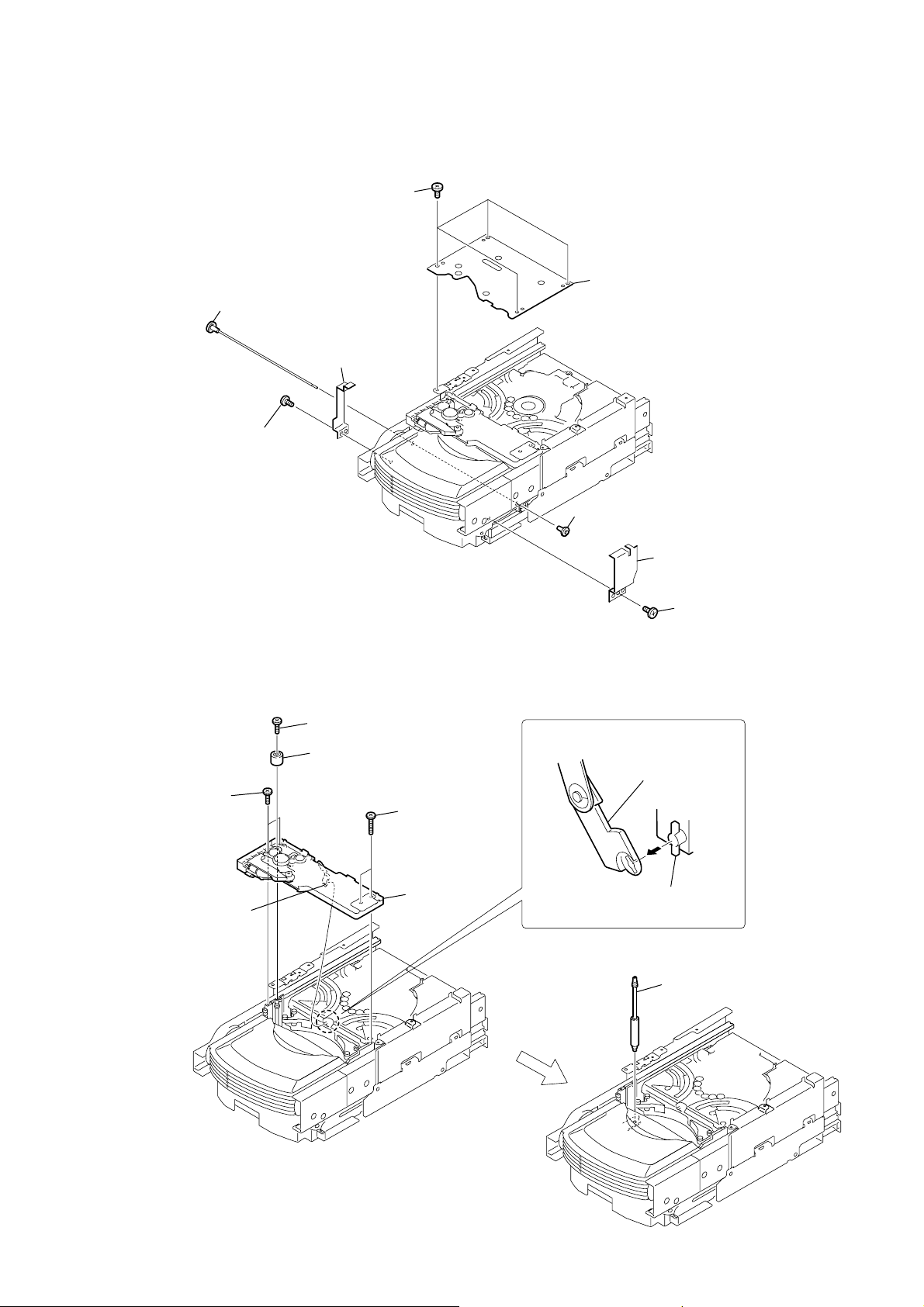
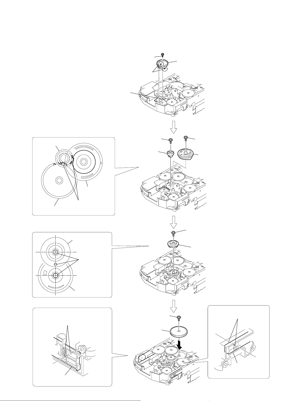
3-33. CHASSIS (TOP), CHASSIS (BOTTOM)
)
4
3
two screws
(P2
5
chassis (top)
three screws
(BVTP2.6
×
10)
×
8)
1
screw
(BVTP2.6
2
lever (CL UP2)
HCD-HPX10W
×
8)
7
chassis (bottom
6
four screws
(P3
×
12)
31
Page 32

HCD-HPX10W
)
3-34. LEVER (LOADING R, LOADING L)
6
lever (loading R)
2
SPR-T (loading L) SPR-T (loading R)
5
two hooks
1
3
two hooks
PRECAUTION DURING LEVER (LOADING R/L) INSTALLATION
Align the horizontal position.
lever (loading L)
Install the
both levers so that they move symmetrically.
lever (loading R)
4
lever (loading L
32
Page 33

3-35. DISC STOP LEVER
d
5
two hooks
1
gear (cap)
2
gear (IDL L)
HCD-HPX10W
PRECAUTION DURING DISC STOP LEVER INSTALLATION
hole
chassis (top)
6
disc stop lever
3-36. DRIVER BOARD
3
Remove soldering
from the two points.
4
motor (pulley) assy
(LOD)
3
two claws
4
disc sensor lever
disc stop lever
hole
Install the disc stop lever so that the both holes
are aligned.
2
three screws
(BVTP2.6
5
DRIVER boar
×
8)
1
belt (MOT)
33
Page 34

HCD-HPX10W
3-37. CD BOARD
1
screw
(BVTP2.6 × 8)
4
CD board
3
wire (flat type)
(16 core) (CN102)
2
Remove soldering
from the four points.
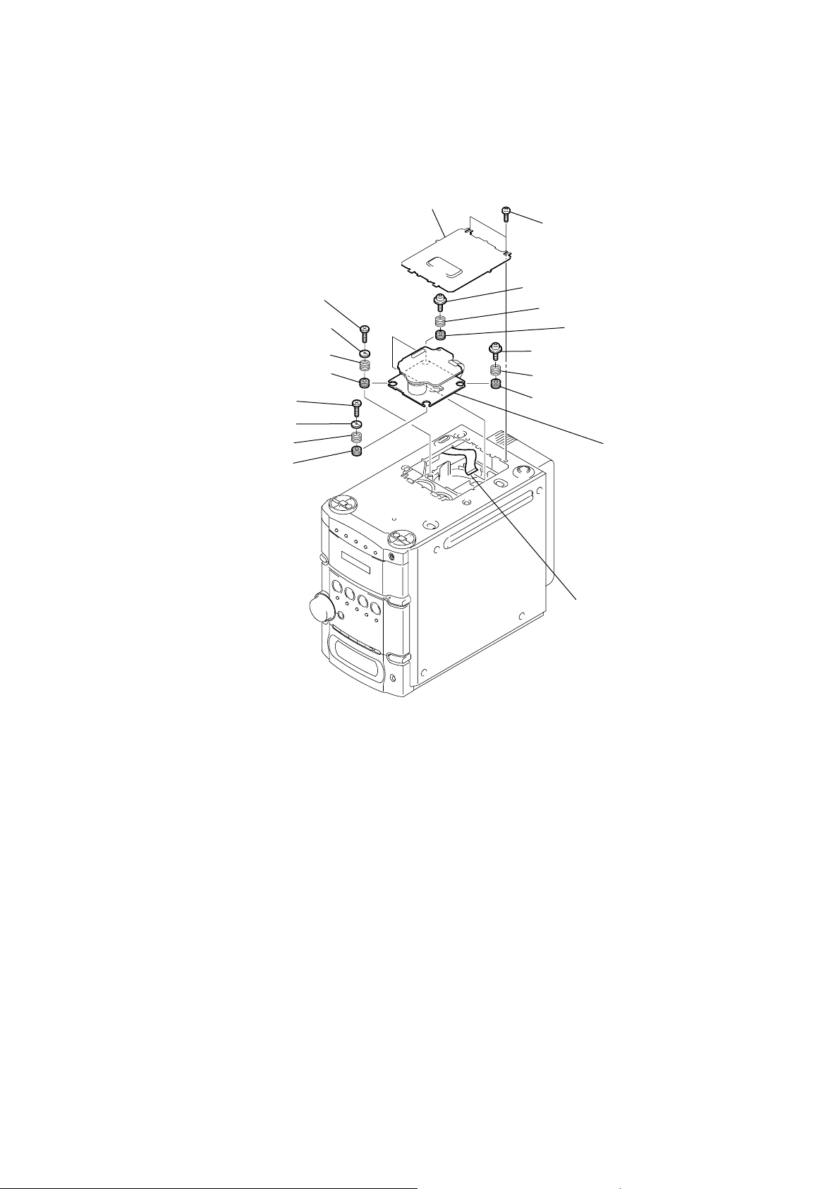
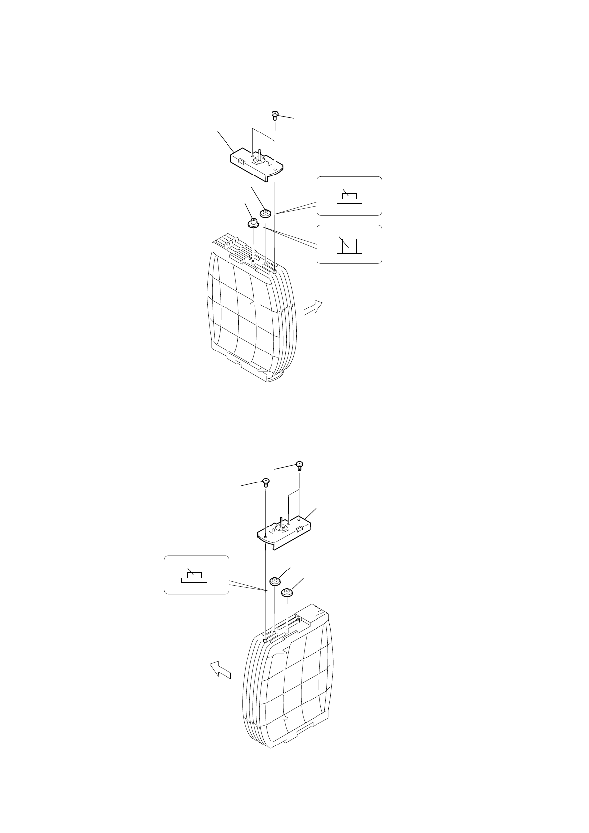
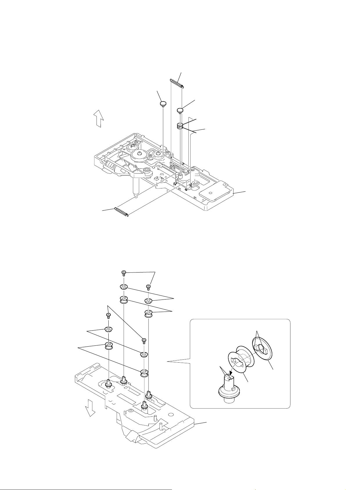
3-38. OPTICAL PICK-UP (KSM-215DCP)
8
optical pick-up
(KSM-215DCP)
4
two floating screws
(PTPWH M2.6)
5
two coil springs (insulator)
7
two insulators
6
two insulators
1
two screws
(BVTP2.6
2
two stoppers (BU)
3
two coil springs (insulator)
×
8)
34
Page 35

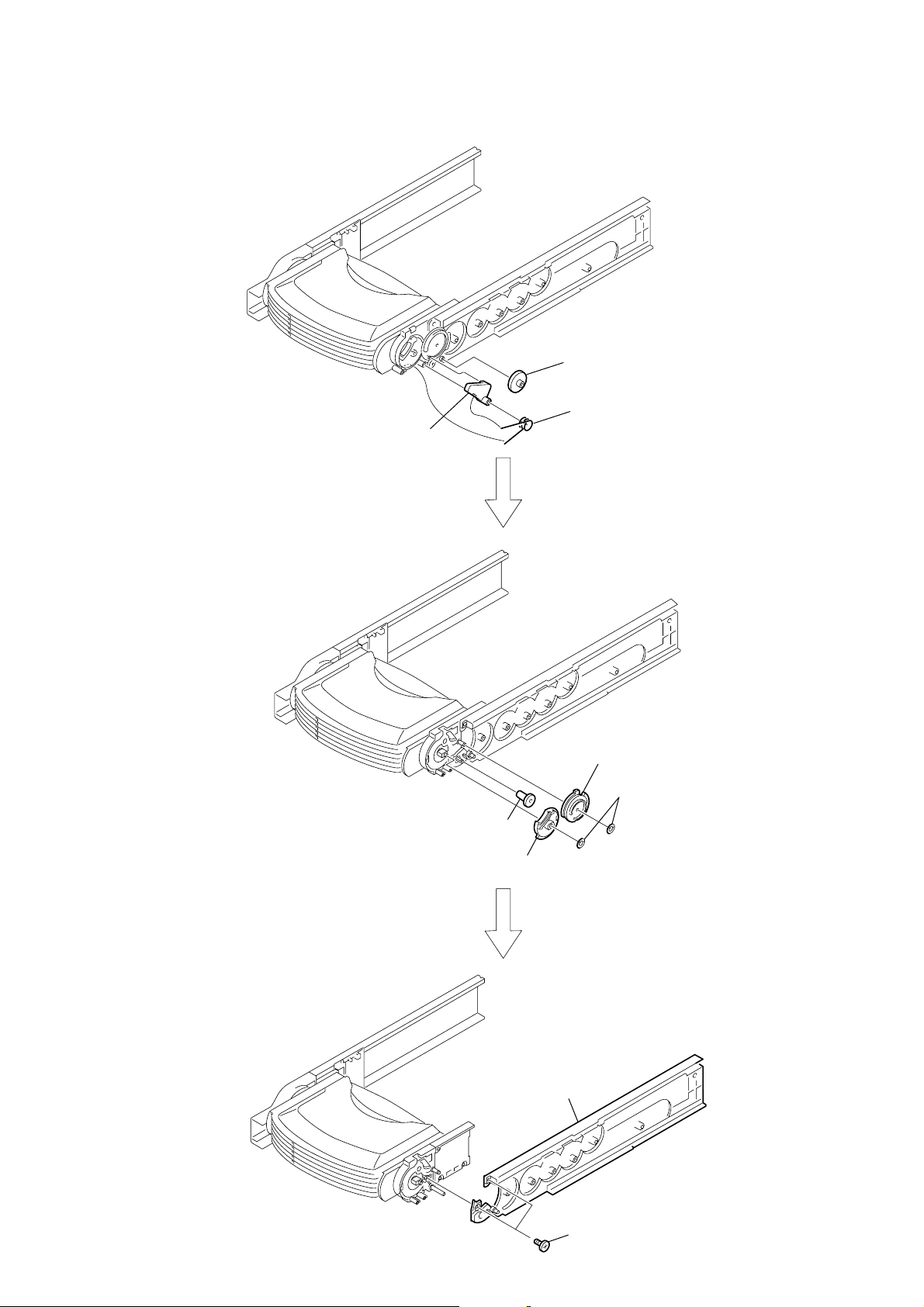
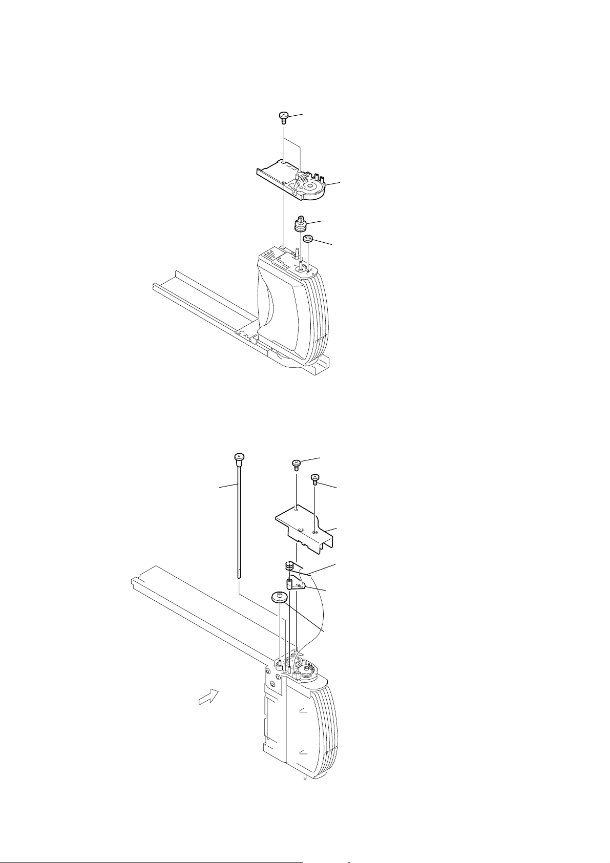
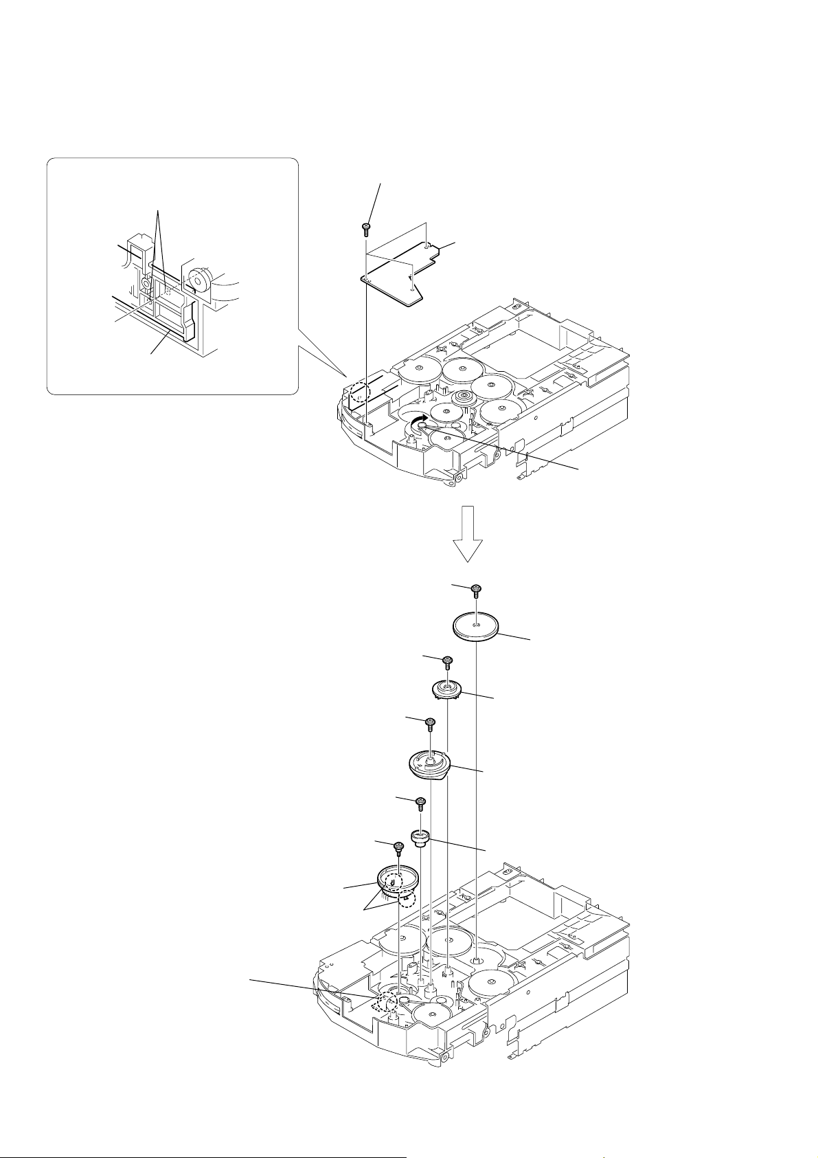
3-39. BASE UNIT SECTION
r
6
Remove the base unit
in the direction of the arrow.
4
floating screw
(PTPWH M2.6)
3
SPR-E 213 down holde
HCD-HPX10W
2
1
screw
(BVTP2.6
3-40. LEVER (BU LOCK)
5
lever (BU lock)
1
gear (cap)
2
gear (BU lock)
lever (CL UP2)
×
8)
5
floating screw
(PTPWH M2.6)
4
three hooks
3
35
Page 36

HCD-HPX10W
3-41. GEAR (IDL-B)
2
claw
1
DIR spring
9
DIR lever
3
gear pulley
4
gear (cap)
5
gear (IDL-A)
q;
gear (IDL B long)
8
stopper
6
Loosen the screw.
7
Hold the Release lever
and change the direction.
3-42. GEAR (IDL-C)
3
gear (IDL-D)
2
two claws
1
gear (IDL-F)
7
gear (IDL-C)
4
three hooks
5
gear loading lever
36
6
claw
Page 37

3-43. SPR-E (TAKO-BACK)
)
two claws
HCD-HPX10W
two claws
parasol
rubber roller
3
four
rubber rollers
1
four screws (2 × 5)
2
four parasols
5
SPR-E (tako-back)
4
tension spring (lower
37
Page 38

HCD-HPX10W
3-44. PLATE (PUSH) ASSY
5
Remove the
in the direction of the arrow.
plate (push) assy
4
four claws
1
SPR-E (plate-push-back)
2
screw (PTPWH M2)
3
gear (tako second)
PRECAUTION DURING GEAR (TAKO SECOND) INSTALLATION
3
SPR-E (plate-push-back)
2
four claws
1
Remove the
in the direction of the arrow.
plate (push) assy
Adjust phases.
plate (push) assy
5
Adjust phases.
plate (push) assy
gear (tako second)
4
gear (tako second)
38
Page 39

3-45. SPR-P (LOCK)
1
claw
2
lever (lock)
3
SPR-P (lock)
HCD-HPX10W
PRECAUTION DURING LEVER INSTALLATION
2
Hold the both ends of the SPSR-P
(lock) with two claws.
1
SPR-P (lock)
3
lever (lock)
4
Pick up the SPR-P (lock) from
the claw and hook it on the lever.
39
Page 40

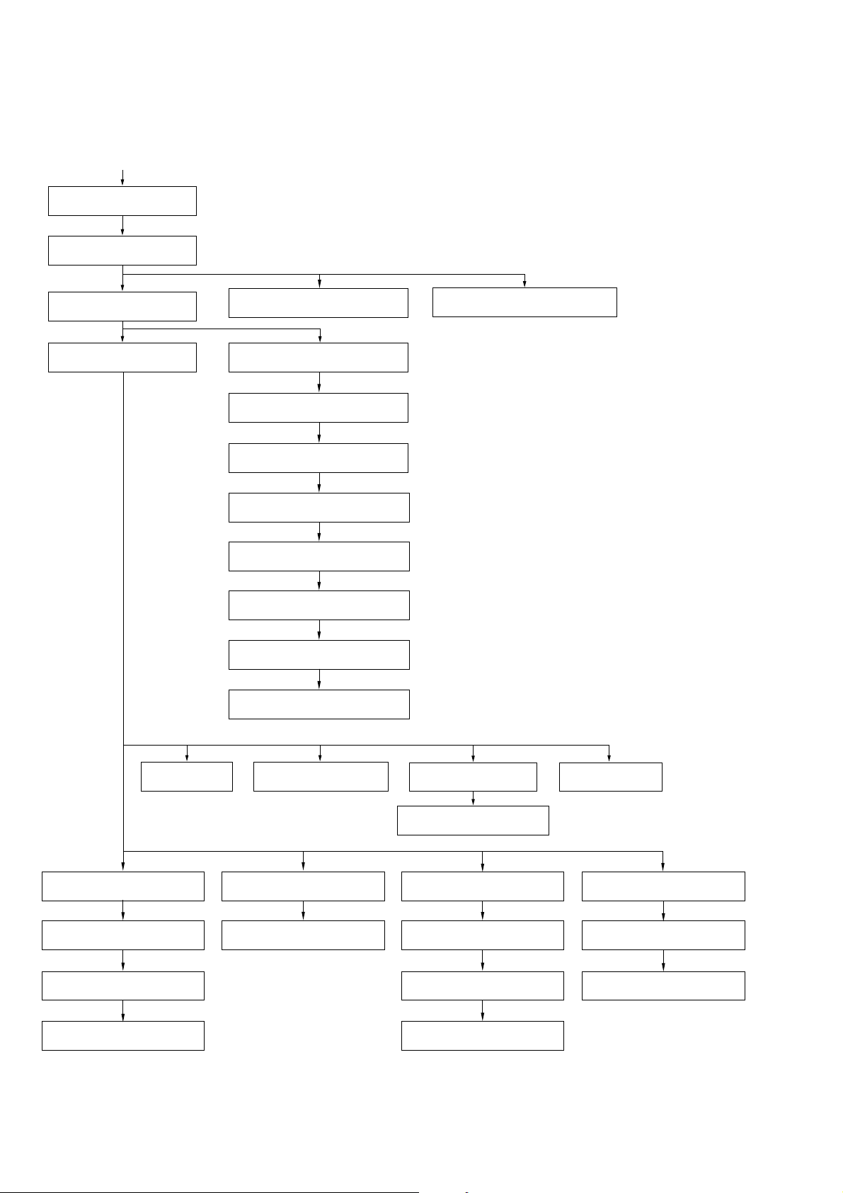
HCD-HPX10W
SECTION 4
ASSEMBLY
•This is can be assemble according to the following sequence.
4-1. ASSEMBLY FLOW
4-2. ASSEMBLING OF THE
STOCKER SECTION (Page 41)
4-3. ASSEMBLING OF THE GEAR
(STOCK RO T SHOR T) (RIGHT) (Page 42)
4-4. ASSEMBLING OF THE GEAR
(STOCK RO T LONG) (LEFT) (P age 43)
4-5. CONFIRMING THE ASSEMBLING
OF THE STOCKER SECTION (Page 44)
4-6. ASSEMBLING OF THE GEAR
(STOCK RO TARY LEFT) (Page 45)
4-7. ASSEMBLING OF THE GEAR
(STOCK RO TARY RIGHT) (Page 46)
4-8. ASSEMBLING OF THE LEVER
(SUB GEAR BACK L) (Page 47)
4-9. ASSEMBLING OF THE GEAR
(SUB GEAR PIN RIGHT) (Page 48)
4-10. ASSEMBLING OF THE LEVER
(SUB GEAR BACK R) (Page 49)
4-11. ASSEMBLING OF THE
SUB GEAR (IDLER) (Page 50)
4-12. ASSEMBLING OF THE
SUB GEAR (2 STEP) (Page 51)
4-13. CONFIRMING THE ASSEMBLING
OF THE ARM SECTION (Page 52)
40
Page 41

4-2. ASSEMBLING OF THE STOCKER SECTION
1
Check the number on each stocker assy,
before assembling all the assys.
HCD-HPX10W
2
stocker (1) assy
6
stocker (1) assy
7
stocker (2) assy
UPPER
SIDE
3
stocker (2) assy
5
tow claws
4
tow dowels
8
stocker (3) assy
9
stocker (4) assy
0
stocker (5) assy
1
Repeat the steps 4 to 6, when installing the part
(2), (3), (4) and (5) of the stocker assy.
41
Page 42

HCD-HPX10W
4-3. ASSEMBLING OF THE GEAR (STOCK ROT SHORT) (RIGHT)
7
short
two screws (2
8
screw (1.7)
UPPER
SIDE
×
6)
Note:
Install the stock box (R) right after
finishing the phase adjustment.
4
gear (stock rot short)
2
gear (stock rot short)
6
stock box (R)
PRECAUTION DURING GEAR (STOCK ROT SHORT) INSTALLATION
1
Align the edges of the stockers. Keep the position of
the stockers until finishing installation of the gear
(stock rot short) and the stock box (R).
FRONT
SIDE
gear (stock rot short)
3
Adjusting the one stockers
42
5
Adjusting the two stockers
gear (stock rot short)
Page 43

4-4. ASSEMBLING OF THE GEAR (STOCK ROT LONG) (LEFT)
6
two screws (2
2
gear (stock rot short)
4
gear (stock rot long)
×
6)
HCD-HPX10W
Note.
Install the stock box (L) right after finishing
the phase adjustment.
7
stocker box (L)
short
long
UPPER
SIDE
PRECAUTION DURING
(STOCK ROT SHORT, STOCK ROT SHORT LONG)
1
Align the edges of the stockers. Keep the position of
the stockers until finishing installation of the gear
(stock rot short) and the stock box (L).
GEAR
INSTALLATION
FRONT
SIDE
5
Adjusting the one stockers
3
Adjusting the two stockers
gear (stock rot long)
gear (stock rot short)
43
Page 44

HCD-HPX10W
4-5. CONFIRMING THE ASSEMBLING OF THE STOCKER SECTION
stocker section
UPPER
SIDE
STOCKER ASSY (R) SIDE
3
Confirm that each claw contacts uniformly at the
respective stop positions of the stocker assy (1) to the stocker assy (5).
4
Confirm the stocker assys move smooth
by sliding the stocker assys (1) to (5)
FRONT
SIDE
Slide the stocker assy in the
1
direction of the arrow.
UPPER
SIDE
44
STOCKER ASSY (L) SIDE
FRONT
SIDE
2
Confirm that each claw contacts uniformly at the
respective stop positions of the stocker assy (1) to the stocker assy (5).
Page 45

4-6. ASSEMBLING OF THE GEAR (STOCK ROTARY LEFT)
2
gear (stock sun)
4
gear (stock planet)
UPPER
SIDE
PRECAUTION DURING GEAR (STOCK PLANET) INSTALLATION
1
Align the edges of stockers,
and keep the position.
FRONT
SIDE
HCD-HPX10W
3
Position to adjust phases
for the gear (stock sun).
Position to adjust phases
5
for the gear (stock planet)
6
Move the arm (L) and the stock
base (B) vertically to the gear.
UPPER
SIDE
7
Check if the stock base (B) is kept
parallel with groove of the stocker.
0
Align the edges of stockers,
and keep the position.
8
gear (stock rotary left)
9
washer (5.5)
The cut-off curve should
face to the front.
45
Page 46

HCD-HPX10W
4-7. ASSEMBLING OF THE GEAR (STOCK ROTARY RIGHT)
0
gear (stock rotary right)
UPPER
SIDE
1
Turn over the
in the direction of the arrow.
stocker assy
qa
washers (5.5)
The cut-off curve should
face to the front.
3
Check that these faces are positioned
parallel to each other.
PRECAUTION DURING GEAR
(STOCK PLANET) INSTALLATION
4
gear (stock sun)
6
gear (stock planet)
5
Position to adjust phases
for the gear (stock sun).
8
stock base (A)
9
two screws
(BTTP M2.6
×
6)
46
2
Keep the position of the edges of
the stockers and adjust phases.
FRONT
SIDE
7
Position to adjust phases
for the gear (stock planet).
Page 47

4-8. ASSEMBLING OF THE LEVER (SUB GEAR BACK L)
1
Turn over the
stocker assy
in the direction of the arrow.
2
Adjust phases.
gear (stock rotary left)
gear (sub gear pin left)
3
gear (sub gear pin left)
4
washers (5.5)
qa
k tapping screw
(2.6
×
8)
0
screw (M2
×
5)
9
cover (L)
7
lever
(sub gear back L)
8
SPR-T
(sub gear back L)
SPR-T (sub gear back L)
gear (stock rotary left)
sub gear (joint just front)
6
lever (joint just front)
gear (sub gear pin left)
5
gear (stock joint),
shaft (stock)
lever (sub gear back L)
PRECAUTION DURING SPR-T
(SUB GEAR BACK L) INSTALLATION
PRECAUTION DURING GEAR
(SUB GEAR PIN LEFT) INSTALLATION
UPPER
SIDE
HCD-HPX10W
47
Page 48

HCD-HPX10W
4-9. ASSEMBLING OF THE GEAR (SUB GEAR PIN RIGHT)
1
Turn over the
in the direction of the arrow.
stocker assy
PRECAUTION DURING GEAR
(SUB GEAR PIN RIGHT) INSTALLATION
UPPER
SIDE
2
Remove the
in the direction of the arrow.
arm (R)
4
two screws
(2
× 5
gear (sub gear pin right)
6
Adjust phases.
gear (stock rotary right)
)
5
gear (sub gear pin right)
gear (stock joint)
7
washers (5.5)
3
two dowels
48
Page 49

4-10. ASSEMBLING OF THE LEVER (SUB GEAR BACK R)
1
sub (joint just front)
2
gear (stock joint)
Note:
Put the driver on the bottom of the other side of the gear,
and push the gear (stock joint) into it. Confirm it is
attached securely .
HCD-HPX10W
3
PRECAUTION DURING SPR-T
(SUB GEAR BACK R) INSTALLATION
claw
5
SPR-T (sub gear back R)
4
lever (sub gear back R)
SPR-T (sub gear back R)
gear (stock rotary right)
gear (sub gear pin right)
claw
lever (sub gear back R)
49
Page 50

HCD-HPX10W
4-11. ASSEMBLING OF THE SUB GEAR (IDLER)
1
of the arrow A until it stops.
4
Position to adjust phases
for the sub gear (idler).
A
Push the sub slider assy in the direction
2
The place that the sub slider assy
stops outside of this.
sub slider assy
3
sub gear (idler)
Note.
The side which has a pattern is the bottom.
4
three sub gears (idler)
Note.
The side which has a pattern is the bottom.
No need of phase adjustment.
50
Page 51

4-12. ASSEMBLING OF THE SUB GEAR (2 STEP)
HCD-HPX10W
1
gear (sub gear pin right)
sub gear (2 step)
hole
hole
hole
PRECAUTION DURING SUB GEAR (2 STEP) INSTALLATION
2
Align the
the
sub gear (2 step)
sub gear (2 step)
gear (sub gear pin right)
gear (sub gear pin right)
and
hole.
5
two screws (M2
4
k tapping screw (2.6
×
5)
3
cover (R)
×
8)
6
arm section
51
Page 52

HCD-HPX10W
4-13. CONFIRMING THE ASSEMBLING OF THE ARM SECTION
2
Check point 1:
The smooth movement of
this part when sliding.
1
Release the lock of the sub slider assy
and slide it in the direction of the arrow.
UPPER
SIDE
Note.
If the two parts of the stopper do not touch the stock base (B) when
the sub slider assy is pushed to the end, the phases are not correctly
adjusted. Reassemble the assy.
6
Check point 3:
Two parts of the stopper
touch the stock base (B).
5
Push the sub slider
assy into the end of
the arm (R).
stock base (B)
3
Check point 2:
All the stocker assy is standing.
4
Slide the stocker assy in the
direction of the arrow.
52
Page 53

SECTION 5
TEST MODE
HCD-HPX10W
[MC COLD RESET]
The cold reset clears all data including preset data stored in the
memory to initial conditions. Execute this mode when returning
the set to the customer.
Procedure:
1. In the standby status, press the @/1 button to turn the po wer
on.
2. Press three buttons of @/1 , x , and [PLAY MODE/TUNING
MODE] simultaneously.
3. The set is reset, and become standby status.
[COMMON TEST MODE]
Enter The Common Test Mode
Procedure:
1. In the standby status, press the @/1 button to turn the po wer
on.
2. Press three buttons of [PLAY MODE/TUNING MODE], x , and
[DSGX] simultaneously.
3. When the common test mode is activated, “SLEEP” and
“PLA Y” icons are blink and “MD” display on the f luorescent
indicator tube.
AMP Test
Procedure:
1. In the common test mode, if turn the [VOLUME] knob
clockwise, it displays “VOL MAX”, and if turn the knob
counterclockwise, it displays “VOL MIN”.
The same operations as described above can also be performed
by pressing the [VOLUME +] and [VOLUME --] buttons of the
remote control.
2. If the [EQ] button of the remote control is pressed, “TONE
MAX” is displayed for several seconds.
Pressing the [EQ] button once more displays the “TONE MIN”,
and another pressing displays “TONE FLAT".
3. “TONE MAX”, “TONE MIN”, and “TONE FLAT” are
displayed repeatedly in this order each time the[EQ] button is
pressed.
4. To release from this mode, press the @/1 button to turn the
power off.
Tape Test
Procedure:
1. In the common test mode, insert a tape.
2. Input any audio signal from the [VIDEO/MD] jack (J301) on
the MAIN board.
3. Press the z REC button, and press the N TAPE button to
select the tape direction.
4. Press the z REC button again to start recording.
5. If press the lm TUNING– or TUNING+ ML
button, the tape is returned to recording start point by cue or
review operation, and starts playback.
6. To release from this mode, press the @/1 button to turn the
power off.
[PANEL TEST MODE]
Enter The Panel Test Mode
Procedure:
1. In the standby status, press the @/1 button to turn the po wer
on.
2. Press three buttons of [REPEAT/FM MODE], x , and [DSGX]
simultaneously.
3. When the panel test mode is activated, LEDs and segments of
fluorescent indicator tube are all turned on.
Version Check
Procedure:
1. In the panel test mode (all LEDs and segments of fluorescent
indicator tube are turned on), press the [REPEAT/FM MODE]
button.
2. Destination indication and model type indication are displayed
on the fluorescent indicator tube alternately.
3. From this status, each time the [TUNING MODE] button is
pressed, it changes the version display of module as follows.
4. To date of module, press the [DSGX] or [FUNCTION] button.
5. To release from this mode, press three buttons of [REPEAT/
FM MODE], x , and [DSGX] simultaneously.
Key Check
Procedure:
1. In the panel test mode (all LEDs and segments of fluorescent
indicator tube are turned on), press the [PLAY MODE/TUNING
MODE] button.
2. It displays “K 0 V0” on the fluorescent indicator tube.
3. Each time a button is pressed, “K” value increases. However,
once a button is pressed, it is no longer taken into account.
All keys are pressed, display becomes “K25”.
4. “V” value increases like 1, 2, 3 ... if turn the [VOLUME] knob
clockwise, or it decreases like 0, 9, 8 ... if turn the knob
counterclockwise.
5. To release from this mode, press three buttons of [REPEAT/
FM MODE], x , and [DSGX] simultaneously.
[CD REPEAT 5 LIMIT CANCEL MODE]
Number of repeat for CD playback is 5 times when the repeat mode
is “REPEA T”. This mode enables CD to repeat playback for limitless
times.
Procedure:
1. Press the @/1 button to turn the power on.
2. Press the [FUNCTION] button to select CD function.
3. Press three buttons of TUNING+ ML , [PLAY MODE/
TUNING MODE], and [DSGX] simultaneously.
4. It enters the CD repeat 5 limit cancel mode and display “LIMIT
OFF”
5. To release this mode , press the @/1 button to turn the power
off.
53
Page 54

HCD-HPX10W
[CD SHIP MODE]
This mode can run the CD sled motor optionally. Use this mode , for
instance, when cleaning the optical pick-up.
Procedure:
1. Press the @/1 button to turn the power on.
2. Press the [FUNCTION] button to select CD function.
3. Press three buttons of [EX-CHANGE] and @/1 simultaneously.
*1
4. Set to the CD ship mode. (chucking on)
5. After blink “STANDBY”, “LOCK” is displayed, disconnect
the AC plug.
*1) If press three buttons of [DISC SKIP], [EX-CHANGE] and
[PLAY MODE/TUNING MODE] simultaneously, Activ ate the
CD ship mode and MC cold reset.
[CD SLOT LOCK]
This mode is for the antitheft of CD disc in shop. (not for transport)
Procedure:
1. Press the @/1 button to turn the power on.
2. Press the [FUNCTION] button to select CD function.
3. Insert a disc.
4. While pressing the x button, press the A (CD) button for
more 5 seconds.
5. The message “LOCKED” is displayed and the disc slot is
locked. (Even if exiting from this mode, the disc slot is still
locked)
6. If press the A (CD) button to eject the disc, the message
“LOCKED” is displayed and can not eject the disc.
7. To release this lock, while pressing the x button, press the
A (CD) button for 5 seconds again.
8. The message “UNLOCKED” is displayed and the disc slot is
unlocked.
[MD/VIDEO FUNCTION CHANGE]
Select either VIDEO or MD of the external input.
Procedure:
1. Press the @/1 button to turn the power on.
2. Press the [FUNCTION] button to select MD or VIDEO function.
3. Press the @/1 button again to turn the power off (standby).
4. While pressing the [FUNCTION] button, press the @/1 button.
5. The another function of the previous function is selected and
display “MD” or “VIDEO”.
[CD POWER MANAGE]
This mode is for switch the CD power supply on/off. Even if this
state pulls out AC plug, it is held.
Procedure:
1. Press the @/1 button to turn the power on.
2. Press the [FUNCTION] button to select CD function.
3. Press the @/1 button again to turn the power off (standby).
4. While pressing the x button, press the @/1 button.
5. It turns power on and display “CD POWER”, then display
“ON” or “OFF”.
[CHANGE-OVER THE AM TUNING INTERVAL]
(except AEP, UK models)
The AM tuning interval can be changed over 9 kHz or 10 kHz.
Procedure:
1. Press the @/1 button to turn the power on.
2. Press the [TUNER/BAND] button to select TUNER (AM)
function.
3. Press the @/1 button again to turn the power off (standby).
4. While pressing the TUNING+ ML button, press the
@/1 button.
5. It turns power on and display “STEP 9kHz” or “STEP 10kHz”,
and thus the tuning interval is changed over.
54
Page 55

SECTION 6
ELECTICAL ADJUSTMENTS
HCD-HPX10W
DECK SECTION
1. Demagnetize the record/playback head with a head
demagnetizer.
2. Do not use a magnetized screwdriver for the adjustments.
3. After the adjustments, apply suitable locking compound to
the parts adjust.
4. The adjustments should be performed with the rated power
supply voltage unless otherwise noted.
5. The adjustments should be performed for both L-CH and RCH.
6. Switches and controls should be set as follows unless otherwise
specified.
REC BIAS ADJUSTMENT
Setting:
digital voltmeter
(AC range)
MAIN board
TP101 (L), TP201 (R)
TP (GND)
Mode: REC
i
JACK (J321)
AF OSC
attenuator
600
Ω
set
blank tap
CS-123
e
Procedure:
1. Connect a digital voltmeter (AC range) to TP101 (L), TP201
(R) and TP (GND) on the MAIN board.
2. Insert a blank tape (CS-123).
3. Press the ?/1 button to turn the power on, and press the
[FUNCTION] button to select TAPE function.
4. Press the [ REC] button twice to start recording.
z
5. Adjust RV101 (L-ch), RV201 (R-ch) on the MAIN board so
that the digital voltmeter reads AC 6.15 V.
6. Connect an oscilloscope or frequency counter to TP101 (L),
TP201 (R) and TP (GND) on the MAIN board.
7. Confirm that the frequency is 82 kHz ±3 kHz.
Adjustment Location:
– MAIN BOARD (Conductor Side) –
REC BIAS ADJUSTMENT
TP201 (R)
(R-CH) (L-CH)
RV201 RV101
TP101 (L)
TP (GND)
55
Page 56

HCD-HPX10W
CD SECTION
Note:
1. CD Block is basically designed to operate without adjustment.
Therefore, check each item in order given.
2. Use YEDS-18 (3-702-101-01) unless otherwise indicated.
3. Use an oscilloscope with more than 10MΩ impedance.
4. Clean the object lens by an applicator with neutral detergent
when the signal level is low than specified value with the
following checks.
S-CURVE CHECK
Oscilloscope
CD board
TP(FE)
TP(VC)
Procedure :
1. Connect an oscilloscope to TP (FE) and TP (VC) on the CD
board.
2. Press the ?/1 button to turn the power ON.
3. Load a disc (YEDS-18) and actuate the focus search. (In consequence of open and close the disc tray, actuate the focus
search)
4. Confirm that the oscilloscope waveform (S-curv e) is symmetrical between A and B. And confirm peak to peak level within
2.0 ± 0.5 Vp-p.
S-curve waveform
symmetry
RF signal waveform
VOLT/DIV : 200mV
TIME/DIV : 500ns
level : 0.7 ± 0.3 Vp-p
– CD BOARD (Conductor Side) –
TP
(VC)
TP
(FE)
IC101
A
±
within 2.0
B
Note: • Try to measure several times to make sure than the ratio of A : B
or B : A is more than 10 : 7.
• Take sweep time as long as possible and light up the brightness
to obtain best waveform.
0.5 Vp-p
Connecting Location: CD board
RFAC LEVEL CHECK
CD board
TP(RFACO)
TP(VC)
Procedure :
1. Connect an oscilloscope to TP (RF ACO) and TP (VC) on the
CD board.
2. Press the ?/1 button to turn the power ON.
3. Load a disc (YEDS-18) and playback.
4. Confirm that oscilloscope waveform is clear and check if RF A C
signal level is correct or not.
Note: Clear RFAC signal waveform means that the shape “◊” can be
clearly distinguished at the center of the waveform.
oscilloscope
TP
(RFACO)
Connecting Location: CD board
56
Page 57

• Circuit Boards Location
d
PANEL (1) board
HCD-HPX10W
SECTION 7
DIAGRAMS
AMP board
POWER board
THERMISTER boar
HEADPHONE board
PANEL (2) board
DISC ADDRESS SW board
ELV MOTOR board
SW board (C)
SW board (D)
MAIN board
DRIVER board
SW board (A)
MOTOR LOD board
CD board
SW board (B)
CONNECTOR board
57
Page 58

HCD-HPX10W
NOTE FOR PRINTED WIRING BOARDS AND SCHEMATIC DIAGRAMS
Note on Printed Wiring Boards:
• X : parts extracted from the component side.
• Y : parts extracted from the conductor side.
• W : indicates side identified with part number.
• f : internal component.
• : Pattern from the side which enables seeing.
(The other layers' patterns are not indicated.)
Caution:
Pattern face side: Parts on the pattern face side seen from
(Conductor Side) the pattern face are indicated.
Parts face side: Parts on the parts face side seen from
(Component Side) the parts face are indicated.
• Indication of transistor.
C
Q
B
B
E
Q
CE
These are omitted.
These are omitted.
Note on Schematic Diagram:
• All capacitors are in µF unless otherwise noted. (p: pF)
50 WV or less are not indicated except f or electrolytics and
tantalums.
• All resistors are in Ω and 1/
specified.
• f : internal component.
• 2 : nonflammable resistor.
• 5 : fusible resistor.
• C : panel designation.
Note: The components identified by mark 0 or dotted
line with mark 0 are critical for safety.
Replace only with part number specified.
• A : B+ Line.
• B : B– Line.
•Voltages and waveforms are dc with respect to ground under no-signal conditions.
•Voltages are taken with a VOM (Input impedance 10 M Ω).
Voltage variations may be noted due to normal production
tolerances.
•Waveforms are taken with a oscilloscope.
Voltage variations may be noted due to normal production
tolerances.
• Circled numbers refer to waveforms.
• Signal path.
F : TUNER (FM/AM)
E : TAPE PLAY
a : TAPE REC
J : CD PLAY
L : AUX IN
•Abbreviation
CND : Canadian model
4
W or less unless otherwise
•Waveforms
– CD Board – – MAIN Board –
IC101 yd (LRCK)
1
IC101 uj (XTAO)
3
Q303, 304 (Collector)
1
(REC Mode)
4.5 Vp-p
21.2
µ
s
Q303, 304 (Base)
2
22.8 µs
IC101 yh (BCK)
2
4.4 Vp-p
59 ns
IC101 ra (PFACO)
4
(REC Mode)
4.5 Vp-p
472 ns
Approx.
700 mVp-p
21.2
µ
s
IC306 qa (XCOUT)
3
30.4
µ
s
12.4 Vp-p
2.6 Vp-p
3.2 Vp-p
IC306 qd (XOUT)
4
62.6 ns
IC306 of (TC END SW)
5
(Tape Play Mode)
2 s
2 Vp-p
6.3 Vp-p
58
Page 59

7-1. BLOCK DIAGRAM — CD SERVO SECTION —
HCD-HPX10W
DETECTOR
A
B
C
D
F
E
OPTICAL PICK-UP
BLOCK
(KSM-215DCP)
LASER DIODE
PD
2-AXIS
DEVICE
(TRACKING)
(FOCUS)
I-V AMP
LD
M101
(SPINDLE)
M102
(SLED)
M
M
CD +3V
AUTOMATIC
POWER
CONTROL
Q10
CH4OUTF
16
CH4OUTF
15
CH3OUTF
17
CH3OUTR
18
CH1OUTF
14
CH1OUTR
13
CH2OUTF
12
CH2OUTR
11
A
26
B
27
C
28
D
29
F
20
E
19
LD
36
MOTOR/COIL DRIVE
IC251
MOTOR
DRIVE
MOTOR
DRIVE
COIL
DRIVE
COIL
DRIVE
MUTE
20
CH4IN
CH3FIN
CH3RIN
CH1FIN
CH1RIN
CH2FIN
CH2RIN
SUMMING
AMP
FOCUS
ERROR
TRACKING
ERROR AMP
APC LD
AMP
24
23
21
4
5
5
7
RF
AMP
FILTER
CD DSP
IC101 (1/2)
AC_
SUM
34
FEO
24
TEO
22
PD
37
OPIN+
OPOUT
27
SFDR
9
SRDR
10
TFDR
11
TRDR
12
FFDR
13
FRDR
14
EQ_
IN
35
2
CD DSP
IC101 (2/2)
PWM GENERATOR
FOCUS/TRACKING/SLED
S101
(LIMIT)
RFAC
VCA
21 23
TEI
CONVERTER
FOCUS/
TRACKING/SLED
SERVO DSP
A/D
EQ
FEI
SSTP
7
RFACO
41
SERVO AUTO
SEQUENCER
TO CPU INTERFACE
MIRR,
DFCT, FOK
DETECTOR
SERVO
INTERFACE
42
MIRR
COUT
SCLK
RFACI
DIGITAL
CLV
PROCESSOR
MDP
6
FOK
DFCT
119
108
45 46
ASYI
ASYMMETRY
CORRECTOR
100
3
1
2
ASYO
XRST
51 53
PCO
FILO
CLTV
DIGITAL PLL
TO SERVO AUTO
SEQUENCER
DATA
CLOCK
38
34 23
CD DATA
CD XRST
22
1125052
FILI
XPCK
CPU INTERFACE
SCOR
SENS
XLAT
CD CLK
SYSTEM CONTROLLER
SBSO
98 99115107102 105 104 110 111
CD XLT
CD SENS
CD SCOR
IC306 (1/3)
EFM
DEMODULATOR
SUBCODE
PROCESSOR
SQCK
SQSO
EXCK
96 97
CD MIDIN
CD MIDIO
CD MICK
CD MICS
CD MIACK
CD MP3REQ
CD MILP
CD MP3RST
CD MP3STB
XTCN
CD AMUTE
32K
RAM
INTERNAL BUS
WFCK
XUGF
GFS
113
36
35
37
26
32
27
25
33
28
55
39
60CDM80 LOAD-IN
59CDM80 LOAD-OUT
63(OUT SW) CDM80 SW1
65(CHUCK SW) CDM80 SW2
48(OPEN) SW1
46(CLOSE) SW2-1
47(LOD POSITION) SW2-2
45(PUSH-CLOSE) SW3
52LOD POS
51LOD NEG
40ELV E3
41ELV E2
42ELV E1
43ELV E0
50ELV POS
49ELV NEG
2CD DISCSENS1
R851-856
1CD DISCSENS2
R857-862
EMPH
68
6
7
4
8
36
5
2
3
DAC
DAC
ERROR
CORRECTOR
MP3 DECODER
IC301
MIDIO
MICK
MICS
MIACK
PO11/BUCK/AD14
MILP
RESET
STANDBY
ROTARY
ENCODER
D/A
DIGITAL
INTERFACE
S701(OUT)
S702(CHUCK)
S811(OPEN)
S821(LOD POSITION/CLOSE)
S831(PUSH-CLOSE)
S841(8cm)44(8cm) SW4
S851(12cm)61(TRIGGER SW) CDM80 SW3
S881
ELV
S861(DICS 1)
S862(DICS 2)
S863(DICS 3)
S864(DICS 4)
S865(DICS 5)
S866(DICS(+1))
117 93
C4M
SELECTOR
LRCK
63 66 65
16
19
18 14
SBSY/BCKIB
SFSY/LRCKIB
D/A
CONVERTER
BCK
PCMD
15
SDI0
BCKIA
LRCKIA
XTSL
CLOCK
GENERATOR
LRCKI
62 60 61
XTAO
XTAI
XTACN
AOUT1
AOUT2
BCKI
PCMDI
1124 19
SDO0
LOADING MOTOR DRIVE
IC701
7 FIN
9 RIN
LOADING MOTOR DRIVE
IC801
7 FIN
9 RIN
ELEVATOR MOTOR DRIVE
IC811
7 FIN
9 RIN
77
78
95
81
86
4OUT1
2OUT2
4OUT1
2OUT2
4OUT1
2OUT2
R-CH
CD MUTING
X171
16.9344MHz
MUTING
Q102
CONTROL
Q317, 318
M701
M
(LOADING)
M871
M
(LOADING)
M881
M
(ELV)
CD
R-CH
• R-ch is omitted due to same as L-ch.
• SIGNAL PATH
: CD PLAY
A
HCD-HPX10W
5959
Page 60

HCD-HPX10W
7-2. BLOCK DIAGRAM — MAIN SECTION —
AC DET
HP SW
C
B
HRP350
(REC/PB/ERASE)
L-CH
R-CH
ERASE
R-CH
RV101
REC BIAS
(L)
R-CH
TAPE MECHANISM
DECK BLOCK
M+10V
MM
CAPSTAN/
REEL
TRGM+
7 9
BIAS OSC
T301
CAPSTAN/REEL
MOTOR DRIVE
Q310, 311
PLUNGER
DRIVE
Q308, 309
A
8
REC/PB SWITCH
BIAS OSC
Q303, 304
IC301
CD
4CONT
RIPPLE
FILTER
Q305
TC CONT
TC TRG
MD/VIDEO
LEVEL SHIFT
Q301, 302
REC BIAS
SWITCH
Q306, 307
L
R
BIAS TRAP
T101
BIAS
R/P
J301
R-CH
MD IN L
1
CD IN L
61
TU IN L
63
TAPE IN L
11
PB
OUT L
7
TAPE L
3
REC OUT L
15
19SI18
INPUT SELECT,
TONE CONTROL,
ELECTRICAL VOLUME
IC302
TONE
OUT
EQ
SC
VOL
IN L
36
37
VOL
OUT L
33
MUTING
Q501
MUTING
CONTROL
Q602, 603
THP801
POWER ON
MUTING
Q601
R-CH
D611
TEMPERATURE
DETECT
Q607
D608
POWER AMP
IC601
STANDBY
SWITCH
Q604
D609
PROTECT
SWICTH
Q608
OVER LOAD
DETECT
Q502
+
PROTECT
CONTROL
IC602
OCP
1
OUT
+
R-CH
RELAY
RELAY
Q609
DRIVE
Q610, 611
FAN MOTOR
DRIVE
Q315
R-CH
VP
2
4
CT
OFF SWITCH
3
UNREG
R-CH
RY301
RELAY
B+ SWITCH
Q605, 606
+POWER
OVER LOAD
DETECT
Q316
REGULATOR
+13V
Q324
J321
PHONES
+
L
R
TM301
SPEAKER
IMPEDANCE
USE 6 – 16Ω
+
–
+
–
M301
M
(FAN)
ANTENNA
FM 75Ω
AM
HCD-HPX10W
PACK
F REC
R REC
END SW
PLAY SW
FM/AM
TUNER PACK
TUNED
STEREO
MUTE
RDS DATA
RDS INT
AEP, UK
LOUT
ROUT
CLK
HALF
END SW
PLAY SW
R-CH
DI
DO
CE
ST DIN
ST DOUT
ST CLK
ST CE
TUNED
STEREO
ST MUTE
RDS DATA
RDS INT
AEP, UK
TC TRG
TC CONT
76
77
95
TC TRG
TC CAPM CONT
RDS-CLK68RDS DATA
18
RDS INT
RDS DATA
HALF
END SW
PLAY SW
75
94
78
TC PLAY
TC END SW
TC HALF/REC SW
ST DATA OUT
ST DATA IN
ST CLK70ST CE69ST TUNED68ST STEREO67ST MUTE
71
72
73
ST DIN
ST DOUT
ST CLK
79
TC R/P
BIAS ON
ST CE
TUNED
87
STEREO
ST MUTE
88
EQ CLK
EQ DATA
S301
(TC DOOR)
82
TC DOOR SW
83
SYSTEM CONTROLLER
IC306 (2/3)
LINE MUTE
X IN
15
X302
16MHz
X OUT11XC OUT
13
X301
32.768kHz
10
XC IN
86
84
PROTECT
AMP POWER
85
SP RELAY
• R-ch is omitted due to same as L-ch.
• SIGNAL PATH
: FM
: CD PLAY
: TAPE PLAY
: TAPE REC
: AUX IN
R/P
BIAS
6060
Page 61

7-3. BLOCK DIAGRAM — PANEL/POWER SUPPLY SECTION —
HCD-HPX10W
7DIN
8 CLK
9 STB
FL/LED DRIVER
IC801
GR1 – GR12
SG1 – SG16
31 – 42
14 – 29
1LED1
2LED2
3LED3
4LED4
LED DRIVE
Q801
LED DRIVE
Q802
LED DRIVE
Q803
LED DRIVE
Q809
LED DRIVE
Q804
FL701
FLUORESCENT
INDICATOR
TUBE
D801
CD
N X
D802
TUNER/
BAND
D803
TAPE
N
D807
DSGX
D804
I/1
UNREG
A+9V
M+10V
+9V
REGULATOR
IC304
+10V
REGULATOR
IC901
+POWER
–POWER
RECT
D901
RECT
D902 – 905
D911
F901
F902
T901
POWER
TRANSFORMER
D912
SYSTEM CONTROLLER
IC306 (3/3)
REMOTE CONTROL
RECEIVER
IC802
S701-725
HP SW
B
S803
ROTARY
VOLUME
ENCODER
D317, 318
4
SIRCS IN/
WAKE
KEY1 – KEY3
89 – 91
74 KEY WAKE UP
5 VOL A
6 VOL B
FL DATA
100
21FL CLK
7FL STB
3STBY LED
RESET
AC-CUT
+7V
M+7V
D+4V
D311
AVDD
DVDD
57CD BD POWER
80RY ON
12
20
RESET SWITCH
Q316
D312
B+ SWITCH
Q312, 313
VOLTAGE DETECT
IC305
U-COM B+
D306
D308
SWITCH
Q321
FL –30V
REGULATOR
IC902
+4V
REGULATOR
IC903
CURRENT
LIMIT
Q808
SUB POWER
BLOCK
U COM +B AC
SW
SW 9V
D906 – 909
FL AC
FL AC
–30V REGULATOR
Q805 – 807
RECT
RECT
D910
RY901
RELAY DRIVE
Q319, 320
AC DET
(AC IN)
C
HCD-HPX10W
SW-POWER
B+ SWITCH
Q322, 323
53
D327
A+9V
6161
Page 62

HCD-HPX10W
7-4. PRINTED WIRING BOARD — CD Section —
1 2 3 4 5 6 7 8 9 10 11 12 13 14 15
A
CD BOARD
(COMPONENT SIDE)
B
C302
C303
C
C305
R313
C315
C316
R302
D
C314
C312
C182
C184
C183
C209
C318
C151
C210
R165
X171
R162
C174
R171
C172
R191
R173
R172
C171
C134
L301
E
FB301
R205
F
R201
C201
C203
G
H
• See page 57 for Circuit Boards Location. :Uses unleaded solder.
C255
C196
R405
R354
C308
R351
R121
C123
C125
C195
R352
R353
C15
C10
C11
C16
C258
C259
Q10
C18
E
C257
C14
R11
R12
R13
R10
R253
C116
C17
C260
1-860-502-
12
(12)
CD BOARD
(CONDUCTOR SIDE)
C252
28 22 21 15
IC251
17 814
R252
R251
C251
(VC)
C114
TP
C113
R113
C112
C111
R114
TP
(FE)
CN101
R112
M101
M
(SPINDLE)
31
IC303
45
S101
(LIMIT)
R404
C306
C313
116
C163
C133
R133
C310
C212
C132
4833
R163
C143
R141
R143
17
C320
C115
R111
R307
C307
C309
R411
120 91
1
30
31 60
C122
TP
(RFACO)
32
C124
IC301
R303
R407
IC101
R132
R419
64
49
C142
C311
R409
C211
90
61
C194
C181
C162
R142
C141
R203
R306
R408
R412
C161
R403
R401
C213
R151
R301
R406
R402
R182
R161
C317
R305
R410
R181
M
C186
C185
R204
27
1
M102
(SLED)
CN201
1-860-502-
12
(12)
A
MAIN
BOARD
CN304
(Page 66)
I
HCD-HPX10W
C131
R131
OPTICAL
PICK-UP
BLOCK
(KSM-215DCP)
• Semiconductor
Location
Ref. No.
IC101 F-12
IC251 D-9
IC301 D-12
IC303 B-13
Q10 H-6
Location
6262
Page 63

HCD-HPX10W
7-5. SCHEMATIC DIAGRAM — CD Section —
C307
R307
0.1
10k
WE/SDO1
SDO2
CS/RAS/
PO12
AD15/CAS/
C314
TP433
MP3VDD
SDO3/OE
PO9/AD12
PO08/AD11
VDDM
SRMSTB
VDDT
AD10
AD9
AD8
PO07/AD7
PO06/AD6
PO05
AD5/
AD4/PO04
47
4V
C311 C309
0.1 0.1
MP3REQ
R303
100k
C310
0.1
FB301
PIO3/IO3
PIO2/IO2
PIO7/BUS3/IO7
PIO6/FI3/BUS2/IO7
AD2/PO02
AD3/PO03
C312C313
0.10.1
C302 C303
0.1 0.1
PIO1/SDI3/IO1
PIO5/FI2/BUS1/IO5
PIO4/FI1/BUS0/IO4
PO11/BUCK/AD14
PO10/CCE/AD13
MP3 DECODER
IC301
TC94A34FG-002
AD1/PO01
AD0/PO00
VSS
VDD
CKO/PO13/AD16
C308
47
4V
VOUT
NC
STBY
GND
C305 TP422
220
4V
VSS
PIO0/SDI2/IO0
VDDX
XO
R306
0
VIN
IRQ/FIO
CKI/CLOCK/
XI
+1.5V REGULATOR
TXO
VDD
VSSX
TEST
IC303
BH15FB1WG
SFSY/LRCKIB
MIMD
MP3GND
• See page 58 for Waveforms. • See page 76, 77 for IC Block Diagrams.
R203
0
SDI1/
DATA
SBSY/BCKIB
VSSP
VCOI
R313
LRCKIA
BCKIA
LRCKO
MIACK
MIDIO
STANBY
RESET
220
SDI0
BCKO
SDO0
VSS
VDDT
MICK
MILP
MICS
VDDP
C316C315
0.00220.1
R351
100
C306
0.1
R405
100
MIACK
R404
100
MICK
MIDIO
R419
100
MILP
R403
100
MICS
R402
MP3STB
100
R401
MP3RST
100
C318
0.01
R301
100k
R305
100k
C317
0.01
R354
100
R352
100
R353
100
10k
R302
C161
0.1
C181
0.1
0
R173
C185
470p
C182
0.1
C186
470p
C201
100
10V
TP427
PCMDI
TP103
LRCK
TP104
PCMD
TP105
BCK
DOUT
R161
100
C171 R171
22p 470
C172
R172
AOUT2
1M
C183
R181
22
100
6.3V
C184
R182
22
100
6.3V
C203
C162
100
0.1
10V
27p
AOUT1
C174X171
0.116.9344MHz
BCKI
PCMDI
LRCKI
LRCK
VSS
PCMD
BCK
VDD
EMPH
EMPHI
IOVDD2
DOUT
TEST
TEST1
IOVSS2
NC
XVSS
XTAO
XTAI
XVDD
AVDD1
AOUT1
VREFL
AVSS1
AVSS2
VREFR
AOUT2
AVDD2
NC
IOVDD0
RMUT
LMUT
C131
C142
1500p
C151
100
10V
R151
0
NC
DDCR
AVSS5
NC
XTSL
IOVSS0
R165
0
R143
3.3k
C143
0.1
C141
0.1
R141
4.7k
1k
R142
FILI
PCO
FILO
CLTV
DDVRSEN
XTACN
R162
47k
C210
0.1
C194
0.1
DDVROUT
SQSO
AVDD5
SQCK
0.1
C163
AVSS3
SBSO
EXCK
XRST
SYSM
DATA
C196
100
0.1
R163
C125 R121
0.1 15k
C133
0.01
R133
180k
R132
10k
ASYI
VCTL
VPCO
ASYO
CD DSP
IC101
CXD3059AR
XLAT
VSS
CLOCK
VDD
100p
R131C134
1M0.1
TP125
RFACI
TP124
RFACO
330p
0.47
C124
C132
BIAS
RFACI
AVSS4
RFACO
AVDD3
SENS
SCLK
ATSK
WFCK
XUGF
R191
0
C122C123
0.10.1
LD
NC
PD
RFC
EG_IN
XPCK
GFS
C2PO
SCOR
VDD
AC_SUM
C4M
PDSENS
WDCK
RFDCO
COUT
AVSS0
AVDD0
IOVDD1
FRDR
TRDR
SRDR
SFDR
IOVSS1
LOCK
MIRR
AVDD4
FFDR
TFDR
SSTP
MDP
DFCT
NC
NC
D
C
B
A
VC
FEO
FEI
TEO
TEI
F
E
NC
VSS
FOK
JPO10 R11
APC 0
R111
JPO102
R113
JPO103
TP425
TP432
TP428
TP429
TP430
TP431
TP423
IOP1
C17
220
1k
1k
4V
Q10
2SB1690KT146
AUTOMATIC
CONTROL
C18
1000p
R112
FEI
TEI
R114
FRDR
FFDR
TRDR
TFDR
SW+
MDP
POWER
1
R13
C16R12
15k
15k
TP424
IOP2
R10
1100k
3.3
D
C
B
A
C111
3300p
C112
470p
C113
3300p
C114
470p
F
E
C115
0.1
FRDR
FFDR
TRDR
TFDR
SRDR
SFDR
MDP
C15
C10
0.1
10
E
C11
10
D
A
B
C
F
TP102
F+
C14
0.1
FC116
100
10V
VC
TP177
C195
0.1
VC
VCC
TP10
E
TP11
TP12
TP13
TP14
E
D
D
A
A
B
B
C
C
F
F
AGND
LD
VR
TP15
PD
PD
TP16
F+
F+
TP17
F-
T+
TP18
T-
T-
TP19
F-
F-
CN101
16P
TP426
SW-
S101
(LIMIT)
(Page 68)
CN201
27P
M+7V
MGND
MGND
MP3STB
MP3REQ
MIACK
MICK
MIDIO
MILP
MICS
MP3(3.3V)
MP3RST
MP3GND
SCOR
SENS
CLK
XLT
DATA
XRST
XTCN
AVDD(3.3V)
ROUT
AGND
LOUT
DGND
DOUT
DVDD(3.3V)
TP401
TP402
TP403
TP405
TP408
TP415
TP414
TP186
TP187
TP404
TP406
TP407
TP417
TP416
TP413
TP412
TP419
TP434
TP410
TP411
TP409
XRST
XTACN
MVDD
MGND
MP3STB
MP3REQ
MIACK
MICK
MIDIO
MILP
MICS
MP3RST
0
R205
SCOR
SENS
CLK
XLT
DATA
XRST
XTCN
AVDD
ROUT
LOUT
DOUT
R204
MP3STB
MP3REQ
MIACK
MICK
MIDIO
MILP
MICS
MP3RST
R411
100
SCOR
CLOCK
XTACN
C212
SENS
22p
XLT
C211
DATA
220p
XRST
AOUT2
AOUT1
DOUT
R410
100
R409
100
R408
100
R407
100
R406
100
R412
100
TP435
DVDD
C213
22p
C320
0
AVDD
AGND
DGND
TP436
TP420
TP421
C209
R201
0.01
CLOCK
DATA
MDP
SENS
XLT
MOTOR/COIL
DRIVE
IC251
BA5947FM
SCOR
R253TP418
10kGAIN_SW
JPO004C251R252R251
MDP6800p22k10k
OPIN-
OPIN+
PREVCC
OPOUT
TFDR
SW
OUTVREF
TRDR
CH1FIN
CH4CAPA
CH1RIN
CH4IN
FRDR
FFDR
CH2FIN
CH2RIN
CH3RIN
CH3FIN
SFDR
SRDR
C259
0.1
F+T+T+T-T-
F-
C258
0.1
C257
GND
CNF4
POWVCC
CH2OUTF
CH2OUTR
CH1OUTR
GND
POWVCC
MUTE
CH3OUTR
CH3OUTF
CH4OUTF
CH1OUTF
CH4OUTR
0.1
C252
0.1
C255
0.1
C260
220
10V
TP250
TP251
TP252
TP253
SP-
SP+
SL+
SL-
M101
(SPINDLE)
M102
(SLED)
No mark : CD PLAY
HCD-HPX10W
6363
Page 64

HCD-HPX10W
7-6. PRINTED WIRING BOARD — CD MECHANISM Section —
12
34567891011
A
(LOD POSITION/CLOSE)
B
C
(8cm)
• See page 57 for Circuit Boards Location. :Uses unleaded solder.
IC801
DRIVER BOARD
IC701
S702
(CHUCK)
S701
(OUT)
M701
M
(LOADING)
C705
R702
19
D701
R701
C711
CN701
B
MAIN
BOARD
CN303
(Page 66)
1-688-337-
D
E
F
G
(12cm)
(OPEN)
(PUSH-CLOSE)
M
(DISC (+1))
(DISC 5)
(DISC 3)
IC811
MAIN
BOARD
CN315
(Page 66)
M
(DISC 1)
(DISC 2)(DISC 4)
ELV
(ELV)
H
HCD-HPX10W
(LOADING)
6464
Page 65

HCD-HPX10W
7-7. SCHEMATIC DIAGRAM — CD MECHANISM Section —
CN861
S861
S862
S863
S864
S865
S866
7P
CN808
7P
• See page 78 for IC Block Diagram.
IC811
BA6956AN
IC801
BA6956AN
IC701
R851
R853
R855
R857
R859
4.7k
4.7k
4.7k
R852
R854
R856
10k
22k
47k
C821
100
16V
R861
4.7k
4.7k
4.7k
R858
R860
R862
10k
22k
47k
C705
0.01
R702
100
MTZJ-T-77-6.2A
CN801
M701
21P
BA6956AN
CN701
7P
C711
R701
680
D701
10
50V
TP701
SW5
TP702
S702S701
GND
C851
0.01
CN871
CN821
2P
CN811
3P
3P
M871
S811
S831
S821
CN802
2P
CN804
CN805
R802
100
R812
100
D811
MTZJ-T-77-5.1A
3P
3P
R811
470
D801
MTZJ-T-77-6.2A
R801
470
C802
47
16V
C841
0.01
CN807
7P
CN806 CN841
2P 2P
CN881
5P
S841
M881
CN851
2P
S851
S881
HCD-HPX10W
6565
Page 66

HCD-HPX10W
7-8. PRINTED WIRING BOARD — MAIN Section —
1 2 3 4 5 6 7 8 9 10 11
A
MAIN BOARD
S301
(TC DOOR SW)
S301
JW136
JW135
JW224
JW129
B
Q305
Q306
EE
R306
R308
R310
C304
C306
R309
C
H
PANEL (1)
D
BOARD
CN801
(Page 72)
Q307
E
C305
CN310
C318
C105
R103
JW148
R104
R105
19
18
E
D
AMP
BOARD
CN601
(Page 70)
F
JW398
R307
R128
R303
C109
JW146
R228
R106
T101
C319
E
C309
C228
C317
R305
Q304
C307
C107
CN306
R326
C205
C320
D331
JW147
C371
C128
C207
C110
Q303
T201
C372
R206
C224
C308
R203
R304
C125
E
R108
R107
C303
R302
C310
T301
R204
IC301
R205
C209
C210
R208
C212
C111
C112
C211
R210
R207
C213
R209
C113
R109
R110
17 16
IC302
32
33
48 49
C225
R214
C123
R114
C223
G
• See page 57 for Circuit Boards Location. :Uses unleaded solder.
TP101 (L)
R301
C114
R212
JW247
JW158
C119
JW245
JW236
R320
RV101RV201
JW143
Q302
E
C215
R211
JW157
JW156
TAPE MECHANISM
DECK BLOCK
SUPPLIED WITH THE
ASSEMBLED BLOCK
JW242
CN317
R319
R318
R325
18
E
JW142
JW246
C103
JW155
JW212
JW207
JW153
JW211
Q301
9
JW151
JW208
JW209
JW243
R321
R322
R323
JW144
JW169
R324
C102
C202
JW154
JW162
JW163
JW164
JW165
JW168
D301
JW133
E
JW160
JW161
Q310
JW223
JW166
JW167
JW128
JW229
JW120
JW121
JW122
JW123
JW126
JW127
JW150
JW228
R314
JW171
JW173
JW174
E
Q318
JW227
JW225
Q313
21
E
E
C325
JW175
R311
Q308
C314
R475
C335
C334
D307
R331
R375
R374
E
E
Q317
R226
CONNECTOR
BOARD
CN801
(Page 64)
JW130
R373
R333
C333
JW131
JW178
R372
Q312
R126
C238
R312
R315
R406
JW176
Q202
Q311
JW179
E
Q102
R224
R223
CN315
L
R420
E
JW117
R379
R363
R489
R490
R491
R404
R405
D309
D312
D311
JW118
JW119
112
Q309
C331
EE
JW115
JW114
JW226
R496
JW180
R484
R370
R369
JW181
JW183
JW185
D306
13
54
FB305
JW184
R335
D302
1
JW182
FB306
C339
C338
C337
D303
FB303
EXCEPT AEP,UK
R409
R330
D310
R124
R401
R402
R332
R334
C138
Q314
E
IC305
C362
D308
R123
C237
R227
C124
R127
C203
C214
1
64
C222
ERASE HEAD
C106
C206
TP201 (R)
JW140
JW141
1
JW132
C115
R112
R111
C117
C118
C122
HRP350
REC/PB/
R113
C216
C116
R213
C218
C219
(CHASSIS)
CN301
TP (GND)
C217
JW159
R368
R364
FB304
C137
D330
D329
D319
R412
D304
R422
JW234
R495
X301
R411
C353
R366
D305
CN307
R494
C336
R423
G
C330
R365
R425
JW217
R424
C367
JW186
R413
C347
C349
POWER BOARD
CN901
(Page 74)
JW110
C394
JW113
D318
R367
100
1
X302
R417
JW197
R419
JW200
R426
C343
JW218
JW124
C345
JW219
JW220
JW112
R474
D317
R418
R427
FB302
C342
JW221
JW111
R391
R482
IC306
R428
EXCEPT AEP,UK
R336
R429
CN411
C348
C393
C344
C131
JW108
8081
R430
JW109
C346
R390
R118
R337
C231
R472
3130
C350
R469
R468
R218
C141
R378
R432
C351
C391
JW196
JW199
FB301
JW201
C352
AMP BOARD
F
CN605
(Page 70)
13
CN316
JW103
JW106
C329
JW105
R433
C354
CN304
C241
C340
C359
R434
JW107
R457
51
50
R450
R449
R448
R440
R438
JW198
R435
C355
C358
R459
R458
R350
R465
R463
R461
R460
1
R451
R441
R436
C356
JW137
JW104
C322
C321
15
CN305 *1
214
JW125
R360
R362
R361
EXCEPT
R377
AEP,UK
R359
R358
R442
R439
R437
C357
JW215
JW216
C368
R443
R347
R444
R342
FB307
FB308
R339
R455
R453
R445
R344
R343
JW195
JW195
R340
JW139
JW188
JW191
R341
R346
R345
JW205
C396
C395
R446
JW170
JW189
R447
JW202
JW204
JW172
JW241
FM/AM TUNER UNIT
SUPPLIED WITH THE
ASSEMBLED BLOCK
JW230
JW231
JW116
D325
*1 CN305
11P:EXCEPT AEP,UK
15P:AEP,UK
R394
E
Q322
JW193
JW152
JW194JW177
JW149
JW214
JW210
CD BOARD
CN201
(Page 62)
JW222
JW102
JW101
R393
Q323
C328
R395
C327
C326
Q321
E
E
C373
A
R381
R382
Q320
C374
Q319
D327
IC304
1
FB309
3
JW134
JW100
D328
E
Q324
R397
Q316
EE
R328
R327
Q315
R329
D326
RY301
CN309
CN308
CN303
B
JW206
JW203
DRIVER BOARD
(Page 64)
L102
C133
C134
L202
JW244
17
CN701
E
L302
1
R396
14
JW240
JW302
1
C101
R102
JW232
JW233
E
C324
JW192
6
C135
C235
1-861-593-
R120
M301
(FAN)
M
CN313
R201
R220
R122
R222
C234
C233
3
C397
R101
C201
D313
(CHASSIS)
R202
+
–
–
+
E
SUB POWER
11
(11)
L
R
TM301
SPEAKER
IMPEDANCE
USE 6-16Ω
AMP BOARD
CN603
(Page 70)
BLOCK
(1/2)
J301
MD/VIDEO
L
R
• Semiconductor
Location
Ref. No.
D301 B-5
D302 E-6
D303 E-6
D304 E-6
D305 E-7
D306 E-6
D307 D-5
D308 E-6
D309 D-6
D310 E-6
D311 E-6
D312 E-6
D313 C-10
D317 C-7
D318 C-7
D319 B-6
D325 C-9
D326 C-10
D327 D-9
D328 B-10
D329 B-6
D330 B-6
D331 E-2
IC301 C-4
IC302 E-3
IC304 B-10
IC305 E-6
IC306 D-8
Q102 F-6
Q202 F-6
Q301 C-4
Q302 D-4
Q303 C-2
Q304 B-2
Q305 B-2
Q306 B-1
Q307 C-1
Q308 B-5
Q309 B-6
Q310 B-5
Q311 B-6
Q312 E-5
Q313 E-5
Q314 D-6
Q315 C-10
Q316 C-10
Q317 F-5
Q318 F-5
Q319 C-10
Q320 C-9
Q321 E-9
Q322 C-9
Q323 C-9
Q324 C-10
Location
HCD-HPX10W
6666
Page 67

HCD-HPX10W
7-9. SCHEMATIC DIAGRAM — MAIN Section (1/3) —
CN305
11P: EXCEPT AEP,UK
15P:AEP,UK
12 RDS +3.3V
13 NC
14 RDS INT
15 RDS DATA
J301
2P
C397
FB309
0.1
• See page 58 for Waveforms. • See page 78 for IC Block Diagram.
C322
220
10V
R101
R201
1k
1k
R102 C101
47k 220p
R202
C201
47k
220p
IC301
BA3126N
C321
0.01
18
58
C141
10
50V
C241
10 50V
R118
4.7k
R218
4.7k
CN306
9P
R391C131
47k470p
R390C231
47k470p
HRP350
CN301
50V
50V
50V
Q301
KRA103M-AT
C203
680p
R301
4.7k
8P
T201
TP
C302
0.01
RV201
220k
(GND)
C206 C106
27p 27p
T301
RV101
220k
TP101TP201
C105
330p
T101
(L)(R)
R303R302
5.65.6
Q305
2SD1387-34-TP
C303
2.2
50V
Q303
2SC2001TP-LK
Q304
2SC2001TP-LK
R306
2.2k
C304
R307
6.8k
C103
680p
R203C205
5.6k330p
R104C107
10k4700p
R103 R105
5.6k 2.2k
10
50V
C305
R205
2.2k
R206C207 R204
47k4700p 10 k
R106
47k
47
16V
C307
0.015
R309
2.2k
KRC102M-AT
Q302
KRC102M-AT
18k
R304
Q306
KTA1266GR-AT
Q307
0.0068
C308
18k
R305
R310
0.0068
C309
10k
C306
50V
JW246 JW247
10 50V
C102
10 50V
C202
C116
0.022
R113
150k
1 50V
1 50V
100k
C212 R209
330p 330k
C112
330p
C111
330p
C213
C117
R127
R227
0.0082
R109
330k
10
50V
C113
0.0082
C217
10
50V
1k
1k
R210C211
470k330p
R110
470k
C317 C319 C320
22
50V
R213
R212R211
150k
5.6k180
C215
10
50V
0.018
C310
R308
22k
10
C115
R108
4.7k
C110
C216
0.022
10
R111
50V
R112
180
5.6k
C114
C214
R207
C210
10
50V
R208
4.7k
C209
10
50V
C109
10
50V
R107
100k
10
50V
10
C218
50V
10
10
10
C219
C118
C119
C122 C222
2700p 2700p
C124
R114
3.3k4750V
C123
0.22
C224
R214
C223
3.3k4750V
0.22
C225
BD3402KS2
470
10V
IC302
C228
10
50V
C318
C371 C372R326
470
0.1 0.1100k
10V
D331
10EDB40
-TA1B2
220
10V
22
50V
C125
22
50V
C128
R228 R128
4.7k 4.7k
10
50V
HCD-HPX10W
6767
Page 68

HCD-HPX10W
7-10. SCHEMATIC DIAGRAM — MAIN Section (2/3) —
Q308
KTA1271Y
CN317
7P
R318
10k
R319
22k
R320
47k
R323
4.7k
R321
4.7k
R322
4.7k
R324
10k
R325
10k
CN303
7P
CN304
27P
C343
C342
2200
0.1
10V
C344
100p
C345
100p
C346
100p
C347
100p
C348
22p
C349
100p
C350
100p
C351
100p
C354
100p
C355
100p
C356
100p
C357
100p
C358
100p
C359
100p
C237 R223
22 50V 1k
C395
C396
2200
0.1
10V
• See page 58 for Waveforms. • See page 80 for IC Pin Function Description.
R311
R312
47k
0.0047
R123
1k
Q310
KTA1271Y
KRC402-RTK
C353
1000
10V
FB306C137
R124
Q309
KRC402-RTK
D301
1SS133T-77
R314
47k
R315
1k
R450
100
R449
100
R448
Q311
Q102
2SC3624-T1L1718
Q202
2SC3624-T1L1718
CN411
R126
R226
Q317
KRA102S
10EDB40-TA1B2
10EDB40-TA1B2
D310
10EDB40-TA1B2
D311
D312
0
0
0
0
FB301
C393
0.1
100k
C391
0.1
R350
4.7k
022 50V
FB304
FB303
R224 C238
100k 220p
C138
FB307
FB308
FB305
Q318
220p
KRC102S
R347
47k
R346
47k
R345
47k
R344
47k
R343
47k
R342
47k
R341
47k
R340
47k
R339
47k
4P
10k
10k
100
R447
100
R446
100
R445
100
R444
100
R443
100
R442
100
R441
100
R440
100
R439
100
R438
100
R437
100
R436
100
R435
100
R434
100
R433
100
R432
100
R337
100
R336
100
D302
1SS133T-77
D303
1SS133T-77
D304
1SS133T-77
D305
1SS133T-77
D306
1SS133T-77
D308
1SS133T-77
R332
4.7k
D307
1SS133T-77
R330
220
C314
JW203
JW240
FB302
0
C352
0.1
C367
C368
1000
0.1
10V
1k
AEP,UK
100
100
100
100
R453
R451
R455
R452
100
100
100
R428
R426
R427
4.7k
4.7k
R429
R430
C333
BD4729GTR
10
50V
R331
10k
EXCEPT AEP,UK
R377
R358 R359 R362
10k
47k 47k 10 k
58
100
100
100
100
100
R461
R460
R457
R459
R458
100
100
100
100
47k
R425
R424
R422
R423
R420
IC305
100
R463
M3062CMEN- A02FPU0
100
10k
100
R419
R418
R417
18
R378
10k
EXCEPT
AEP,UK
47k
R360
100
R465
IC306
X302
16MHz
AEP,UK
C334 R334
0.1 47k
R474
20p
C339
1SS133T-77
1M
100
100
R475
R472
R409
10k
100
R406
X301
32.768KHz
15p
KTC3199GR-TP
D309
10k
R361
100
100
R468
R469
1k
R411
R413
0
C338
R412 R335
1k 10k
R333C335
22k0.1
CN315
21P
R364
D317
1SS133T-77
R482 R496
100 10k
R484 R363
4.7k
R367
*1
*2 R366
4.7K: US,CND
NO MOUNT: AEP,UK
100 10k
R370
R369
R368
R365
R494
R495
R366
*2
R379
10k
3.3k
3.3k
3.3k
R489
0
R490
0
R491
0
150
100
100
C340
0.1
C336
1000
6.3V
C337
0.1
*1 R367
2.2K: US,CND
NO MOUNT: AEP,UK
D318
1SS133T-77
100
10k
100
R402
R404
R405
R372R373
Q314
R401
100
47k47k
C362
0.1
HCD-HPX10W
6868
Page 69

7-11. SCHEMATIC DIAGRAM — MAIN Section (3/3) —
HCD-HPX10W
CN309
6P
L102
L202
C133 C233
0.1 0.1
Q315
KTA1273-Y-AT
RY301
R327
2.2k
Q316
KTC3199GR-TP
R220R120
47k47k
R329
100k
C134
0.1
10
1/2W
D313
1SS133T-77
R328
10k
C324
C234
0.1
R222R122
10
1/2W
R397
C374
4.7
50V
C135
0.01
C235
0.01
EP200
Q324
470
KTC3205-Y-AT
10
D328
50V
MTZJ-T-77-13B
C330
470
10V
33k
R396
TM301
CN313
CN316
CN307
12P
CN308
3P
M301
3P
4P
C325
IC304
TA7809S
C328 C329
2200
10V
D319
1SS133T-77
L302
D326
1SS133T-77
D325
1SS133T-77
Q312
KTA1273-Y-AT
R375 R382
1k 1k
Q313
470
10V
C327C326
0.010.01
KRC102S
R374
R381
47k
47k
Q319
KTA1273-Y-AT
Q320
KRC102S
Q321
KRC102M-AT
50V
C331
470
10V
C394
10
D329
0.1
1SS355TE-17
D327
R395
1SS133T-77
1k
R393
D330
1SS355TE-17
JW398
JW243
Q322
R394
KTA1271Y
1k
Q323
KRC102S
47k
C373
47
35V
CN310
19P
2
1
HCD-HPX10W
S301
6969
Page 70

HCD-HPX10W
7-12. PRINTED WIRING BOARD — AMP Section —
A
B
C
D
E
F
• See page 57 for Circuit Boards Location. :Uses unleaded solder.
1 2 3 4 5
AMP BOARD
CN992
D
MAIN BOARD
CN306
(Page 66)
F
MAIN BOARD
CN316
(Page 66)
J
POWER BOARD
CN902
(Page 74)
E
MAIN BOARD
CN309
(Page 66)
K
HEADPHONE
BOARD
CN311
(Page 72)
THP822
CNJ911
CN601
CN602
CN603
CN604
CN605
1
3
1
7
1
6
1
3
JW609
JW641
IC602
R625
JW606
JW607
JW604
JW610
C609
136
R626
JW612
JW608
D610
C606
C607
4
R624
R615
R513
R514
R564
JW640
R618
C604
C608
JW615
JW644
R616
R620
JW603
R622
JW642
R563
D612
C605
D607
JW621
R617
E
Q608
Q610
Q611
Q605
JW611
R619
R628
Q609
R613
JW616
Q607
E
E
R614
E
C614
JW643
C616
R621
R612
C556
D608
R611
Q606
JW613
E
D609
EE
JW618
D603
C613
C557
R609
R610
R601
JW619
R602
JW602
JW614
JW620
R606
C507
C506
Q603
JW617
E
C611
C610
Q604
C615
R562
R512
E
E
C612
E
JW632
JW623
C603
R607
D611
Q602
R604
R603
R605
R608
R557
Q601
C555
R560
R510
JW630
JW631
JW634
JW622
C505
JW628
JW633
Q552
R553
Q551
E
JW626
JW627
C617
R503
R565
C501
R507
R558
R508
R561
E
R551
R506
JW629
R502
JW625
C553
C503
R511
Q501
E
JW624
R556
C504
Q502
R501
R515
C551
R552
D501
D551
E
1-526-594-
C554
R555
15
R505
C502
1
IC601
R559
R509
C552
11
(11)
• Semiconductor
Location
Ref. No.
D501 F-5
D551 F-5
D603 C-3
D607 B-3
D608 B-3
D609 B-3
D610 B-2
D611 B-4
D612 B-2
IC601 E-5
IC602 B-2
Q501 C-5
Q502 F-5
Q551 C-4
Q552 F-4
Q601 B-4
Q602 C-4
Q603 C-4
Q604 C-4
Q605 C-3
Q606 C-3
Q607 B-3
Q608 B-3
Q609 C-3
Q610 C-3
Q611 C-3
Location
HCD-HPX10W
7070
Page 71

HCD-HPX10W
7-13. SCHEMATIC DIAGRAM — AMP Section —
R501
2.2k
2SC3623ATP-LK
R551
2.2k
R515
100k
R565
100k
C610
C611
22
50V
22
50V
2SC3623ATP-LK
CN601
C617
0.001
9P
• See page 79 for IC Block Diagram.
C502
C501
220p
10
R503
50V
R603
2.2k
Q551
Q501
R601
10k
R604
2.2k
R602
220k
R553
1k
1k
KRA102S
KRC102S
Q601
KRA102S
Q602
Q603
R502
R552
C551
R505
0
470p
R506
1.2K
C504
C503
47
56k
50V
C553
47
56k
50V
R556
1.2K
R555
0
10
C552
50V
22Op
1SS133T-77
D611
C554
470p
R606
D610
Q605
Q606
1SS133T-77
IC602
RT8H015C-T112-1
R622
22k
Q610
KTC3199GR-TP
R614
10k
C605
100
10V
R624
KTC3199GR-TP
IC601
STK433-070
R616
10k
R617
10k
D607
MTZJ-T-77-5.1B
R510
0.22
2W
1
Q604
R507
56k
C505
15p
C603
0.001
R557
56k
C555
15p
R608
100
D603
1SS133T-77
C613
R609
10k
R610
33k
10
50V
R607
C612
R605
4.7k
1
220
50V
KTC3199GR-TP
R508
1k
R509 R511
15k 100k
1SS133T-77
1SS133T-77
R559
15k
R558
1k
D501
D551
R560
0.22
2W
Q502
KTA1266GR-AT
Q552
KTA1266GR-AT
Q607
KTC3199GR-TP
R561
100k
C556
0.22
50V
C614
2200
50V
C615
2200
50V
R618
15k
D609
1SS133T-77
C506
0.22
50V
C507
0.1
R512
10
1/2W
R562
10
1/2W
C557
0.1
D608
1SS133T-77
C616 R628
0.1 470k
R620
4.7k
C604
50V
KTC3199GR-TP
10
Q608
D612
1SS133T-77
R621
100k
R613
10k
R611
10k
R612
100k
R619
1k
Q609
KTC3199GR-TP
KTA1266GR-AT
KTC3199GR-TP
C609
2.2
50V
R626
100
R625
C606
0.001
100
C607
Q611
R615
10
50V
560
2W
1k
C608
R563
100
10V
R513
47k
56k
R514
R564
CNJ991
2P
470
2W
470
2W
THERMISTER
BOARD
CN992
2P
CN603
6P
CN602
7P
CN604
3P
CN605
3P
THP822
HCD-HPX10W
7171
Page 72

HCD-HPX10W
7-14. PRINTED WIRING BOARD — PANEL Section —
12
345678910111213
A
B
C
DISC SKIP
• See page 57 for Circuit Boards Location. :Uses unleaded solder.
EEE
E
(FLUORESCENT INDICATOR TUBE)
3
1
IC802
IC801
E
DISC 3DISC 4DISC 5
AMP
BOARD
CN604
(Page 70)
TAPE
REC
CD SYNC
REPEAT/
FM MODE
PLAY MODE/
TUNING MODE
D
E
F
G
VOLUME
DISC (+1)
+
FUNCTION
DSGX
DISC 1DISC 2
D807
R833
E
• Semiconductor
ALBUM
+
-
E
D802
TUNER/
BAND
D801 D803
E
E
R830
CD
-
R832
TAPE
EX-CHANGE
MAIN
BOARD
CN310
(Page 66)
Location
Ref. No.
D801 F-5
D802 F-4
D803 F-6
D804 C-7
D805 A-6
D806 A-6
D807 E-4
D810 C-6
IC801 B-5
IC802 B-7
Q801 F-5
Q802 F-4
Q803 F-6
Q804 C-7
Q805 A-5
Q806 A-5
Q807 A-5
Q808 A-5
Q809 E-4
Location
HCD-HPX10W
7272
Page 73

HCD-HPX10W
7-15. SCHEMATIC DIAGRAM — PANEL Section —
FL701
C838
220p
220p
C820
220p
C821
0
R845
C822
220p
C823
220p
C824
220p
C825
220p
C826
220p
C827
220p
C828
220p
C829
220p
C830
220p
C831
D801
SLR325DC-P-T32
Q801
KTA1266GR-AT
220p
R830
100
R831 R832 R833
100 100 100
D802
SLR 325D C-P-T32
Q802 Q803 Q809
KRC102S KRC102S KRC102S
C833
0.1
D803
SLR 325DC-P-T3 2
D807
SLR 325DC-P-T32
• See page 79 for IC Block DiagramSection
IC801
PT6315
C837
0.1
C832
10
6.3V
10EDB40-TB3
R849
TP806
R848
82k
C834
0.001
R847
100p
100k
100k
0.001
C835
R846
C836
100
R850
100
R851
100
JW801
0
R861
0
R862
0
D810
JW802
0
S803
IC802
NJL73H400A
CN311
3P
C804
R841
C806C807
0.010.01
0.01
100
C805
10
6.3V
Q804
KRC102S
R835
R842
100
470
D804
SLR325VC-N-T32
RED
D806
MTZJ-T-77-5.1B
R859R860
100100
CN802
R858
10k
2P
R856
10
50V
KTA1266GR-AT
100k
22
R857
C841
C840
100
10V
Q807
KTA1266GR-AT
Q808
R855
4.7k
C839
0.1
50V
R854
4.7k
D805
MTZJ-T-77-33B
Q806
KTA1266GR-AT
C848
Q805
KTA1266GR-AT
0.0047
CN312
R852R853
4.7k4.7k
CN801
17P
0.0047
C846
0.0047
C847
2P
FB122
D131
1SS355TE-17
C236
0.001
50V
0.001 50V
D130
1SS355TE-17
C136
J321
HCD-HPX10W
S720
R809 R808
10k 4.7k
S710
S709
S719 S718
R801R802R803R804R805R806R807
2203304706801k1.5k2.2k
S703S704S705S706S707S708
R811R812R813R814R815R816R817R818R819
2203304706801k1.5k2.2k4.7k10k
S717 S716 S715 S714 S713 S712 S711
CN804
R824
R825R823R822R821
S701S702
CN803
2P
680 1k470330220
S725S724S723S722S721
2P
7373
Page 74

HCD-HPX10W
7-16. PRINTED WIRING BOARD — POWER Section —
12
A
B
C
• See page 57 for Circuit Boards Location.
3456789
AEP,UK
US,CND
:Uses unleaded solder.
AC
IN
JW906
SUB POWER
BLOCK
D
E
F
G
MAIN
BOARD
CN307
(Page 66)
IC903
IC902 IC901
AMP
BOARD
CN602
(Page 70)
• Semiconductor
Location
Ref. No.
D901 F-8
D902 E-6
D903 E-6
D904 E-6
D905 E-6
D906 F-5
D907 F-5
D908 F-5
D909 F-5
D910 E-3
D911 F-6
D912 F-6
D913 E-7
D914 E-5
IC901 E-5
IC902 E-4
IC903 E-4
Location
HCD-HPX10W
7474
Page 75

7-17. SCHEMATIC DIAGRAM — POWER Section —
D914
1N4002B
HCD-HPX10W
CN901
CN902
IC901
TA7810S
C901
470
10V
12P
IC902
TA7807S
C903
470
10V
IC903
C912
220
C904
50V
7P
470
10V
C902
3300
25V
C905
3300
25V
D910
10EDB40-TA1B2
1SS133T-77
D911
R901
C915R909
10 50V2.2k
D902
1N4002B
D903
C907
1N4002B
0.1
50V
1k
D912
1SS133T-77
R902
1k
D904
1N4002B
D905
1N4002B
R905
3.3
1/4W
R904
0.22
1/4W
R903
0.22
1/4W
C909
0.1
50V
D901
D5SBA20
C913
0.1
C914
0.1
D906
1N4002B
D907
1N4002B
D908
1N4002B
D909
1N4002B
F901
*
F902
*
1 F901, F902
T4AL/125V : US,CND
T4AL/250V : AEP,UK
T901
JW904
D913
1SS133T-77
1
*
1
AEP,UK
US,CND
JW901
JW902
JW934
R906
3.3M
JW906
RY901
JW907
CN904
CN903
2P
2P
HCD-HPX10W
7575
Page 76

HCD-HPX10W
• IC Block Diagrams
– CD BOARD –
IC101 CXD3059AR
1
MIRR
2
DFCT
3
FOK
4
VSS
5
LOCK
6
MDP
7
SSTP
8
IOVSS1
9
SFDR
10
SRDR
11
TFDR
12
TRDR
13
FFDR
14
FRDR
15
IOVDD1
16
AVDD0
17
AVSS0
18
NC
19
E
20
F
21
TEI
22
TEO
23
FEI
24
FEO
VC
25
VC
MIRR
DFCT
FOK
COUT
NC
119
120
INTERFACE
PWM
GENERATOR
SERVO
DSP
A/D
CONVERTER
TE
FE
118
SERVO
WDCK
117
C4M
IC251 BA5947FM
WFCK
C2PO
XPCK
SCOR
GFS
114
112
111
113
VDD
116
115
XUGF
ATCK
110
109
108
DIGITAL
CLV
SCLK
SENS
107
VDD
CLOK
106
105
SERVO
AUTO
SEQUENCER
ERROR
CORRECTOR
XLAT
104
CPU INTERFACE
VSS
103
SYSM
DATA
101
102
D/A
INTERFACE
XRST
100
99
D/A
COVERTER
32k
RAM
EXCK
98
SBSO
97
SQCK
96
SQSO
XTACN
95
CLOCK
GENERATOR
DIGITAL OUT
SELECTOR
94
IOVSS0
XTSL
LPF
LPF
LMUT
91
92NC93
90
RMUT
89
IOVDD0
88
NC
87
AVDD2
86
AOUT2
85
VREFR
84
AVSS2
83
AVSS1
82
VREFL
81
AOUT1
80
AVDD1
79
XVDD
78
XTAI
77
XTAO
76
XVSS
75
NC
74
IOVSS2
73
TES1
72
TEST
71
DOUT
70
IOVDD2
69
EMPHI
68
EMPH
67
VDD
66
BCK
65
PCMD
64
VSS
63
LRCK
PREVCC
28
1
27
–
OPIN–
OPOUT
+
2
OPIN+
OUTVREF
26
3
+
SW
CH4CAPA
25
–
INTERFACE
4
CH1FIN
CH4IN
CH3FIN
CH3RIN
23
INTERFACE
INTERFACE
6
CH2FIN
22
7
CH2RIN
21
8
24
5
CH1RIN
IC303 BH15FB1WG
GND
GND
MUTE
20
MUTING
VREF
9
VREFIN
POWVCC
19
10
POWVCC
CH3OUTF
18
D
11
CH2OUTR
CH3OUTR
17
D
D
12
CH2OUTF
CH4OUTF
16
D
LEVEL SHIFT
D D
13
CH1OUTR
CH4OUTR
15
DD
14
CH1OUTF
26
A
27
B
28
C
29
D
30
NC
HCD-HPX10W
31
32
AVDD4
SUM
33
RFDCO
34
PDSENS
AC_SUM
ATT
35
36LD37
EQ_IN
APC
38NC40
PD
EFM
DEMODULATOR
+
VOLTAGE
REFERENCE
2
VIN
−
GND
SUB CODE
PROCESSOR
ASYNMMETRY
EQ
AMP
39
41
RFC
AVSS4
RFACO
CORRECTOR
42
43
RFACI
44
AVDD3
45
BIAS
46
ASYI
47
ASYO
48
VPCO
VCTL
49
50
AVSS3
DIGITAL
PLL
51
52
FILO
CLTV
FILI
DC/DC
CONVERTER
56
57
54
AVDD5
55
DDVROUT
53
PCO
58
AVSS5
DDVRSEN
59
DDCR
NC
62
LRCKI
61
PCMDI
60
BCKI
1
THERMAL
PROTECTION
OVER CURRENT
PROTECTION
CONTROL
BLOCK
3NC4
STBY
5
VOUT
7676
Page 77

IC301 TC94A34FG-002
HCD-HPX10W
VDDP
/RESET
STANDBY
/MICS
/MILP
MIDIO
/MICK
/MIACK/
AD16
VDDT
VSS
SDO0
MIMD
Generator
TEST
60
Timing
Decoder
Instruction
40 bit
round & limitround & limit
XI
59
PRAM
4k word
A0A1
MAC
A2A3
ALU
VDDX
XO
5762 5861 5663 52 50
VCO
x5
PROM
4k word
Control
Program
MXMYMZ
register
AXAY
VSSP
VCOI
64 55 53 51
1
2
3
4
5
6
7
8
9
10
11
MCU I/F
VSSX
CKO/
PO13/
AD16
Y0/Y1/Y2
XO/X1/X2
VDD
Y-Bus
54
1k bit
X-Bus
VSS
SRAM
PO0/
ERAM
register
X-Pointer
AD0
PO1/
XRAM
4k word
YRAM
4k word
4k wordx12k word
CRAM
4k word
CROM
4k word
AD1
SRAM I/F
x1
x9
PO2/
AD2
PO3/
AD3
PO4/
AD4
49
I/F
SRAM/DRAM
I/F
JTAG
48
47
46
45
44
43
42
41
40
39
38
PO5/AD5
PO6/AD6
PO7AD7
AD8
AD9
AD10
VDDT
SRMSTB
VDDM
PO8/AD11
PO9/AD12
BCKO
LRCKO
SDI0
BCKIA
LRCKIA
37
36
35
34
33
/CCE/
PO10/
AD13
BUCK/
PO11/
AD14
SDO3/
/OE
PO12/
AD15/
/CAS
SDO2/
/CS/
/RAS
Flag
PIO4/IO4
BUS2/FI2/
2sets
Address Calc.
PIO5/IO5
PIO6/IO6
BUS1/FI3/
General
Input/
Output
Port
BUS0/
PIO7/IO7
I/F
CDP
Control
SDO1//WE
IO3
PIO3/
register
Y-Pointer
register
C-Pointer
BUS3/FI1/
12
13
Audio I/F
14
15
16
Sub Code I/F
SDI1
DATA/
SBSY/
BCKIB
SFSY/
LRCKIB
DIT
TXO
VDD
Interrupt
Control
CKI/CLCK/
IRQ/FI0
VSS
Timer
PIO0/
SDI2/IO0
25 26 27 28 29 30 31 3217 18 19 20 21 22 23 24
PIO1/
SDI3/IO1
PIO2/
Bus
Switch
IO2
77
Page 78

HCD-HPX10W
– MAIN BOARD –
IC302 BD3402KS2
1
D1
2
D2
3
E1
4
E2
– CONNECTOR BOARD –
IC801, 811 BA6956AN
1 2 3 4 5 6 7 8 9
VREF
C2
64
INPUT
SELECT
63C162B261
B1
−
+
−
+
OUT2
RNF
– DRIVER BOARD –
IC701 BA6956AN
TSD
CONTROL LOGIC
VCC
A1
FIN
NC
58NC56NC55
57
GND
NC
RIN
LINEOUT153LINEOUT252NC51NC
54
TNF2
TNF1
49
50
48
NC
47
NC
46
NC
45
NC
44
BNF1
43
BOUT1
42
BOUT2
41
BNF2
VM
OUT1
A2
60
59
PBNF2
PBOUT2
PBOUT1
PBNF1
TAPE 1
TAPE 2
RECNF2
RECOUT2
RECOUT1
RECNF1
24
FILTER
+
−
25NC26
ATT
ATT
−
+
−
+
27NC28NC29NC30
NC
40
NC
TONE
CONTROL
TONE
CONTROL
+
−
+
−
31
NC
32
NC
VOLOUT2
39
TONE OUT2
38
VIN2
37
TONE OUT1
36
VIN1
35
NC
34
NC
33
VOLOUT1
−
+
5
−
6
7
8
9
NC
10
NC
11
12
13
14
15
16
+
+
−
−
+
+
−
−
+
BUFFER
−
+
ALC
ALC
DIGITAL
CONTROL
17
18SC19
ALC
20
21
VDD
GND
22
VCC
SI
MIX
−
+
23
NC
78
Page 79

– AMP BOARD –
IC602 RT8H015C-T112-1
OVER LOAD
VCC
6
DETECTDCDETECT
5
GND
HCD-HPX10W
CT
4
1
OCP
– PANEL (1) BOARD –
IC801 PT6315
LED1
1
LED2
2
3
LED3
LED4
4
2 3
VP
VSS
4-bit latch
OUT
VDD
GRID2
GRID1
Grid driver
Command decoder
Display memory
24 bits x 12 words
GRID3
394041424344
GRID4
SEG24/GRID5
12-bit shift register
SEG22/GRID7
SEG23/GRID6
Multiplexed driver
SEG20/GRID9
SEG21/GRID8
3435363738
SEG19/GRID10
33
32
SEG18/GRID11
SEG17/GRID12
31
OSC
DOUT
DIN
CLK
STB
KEY1
KEY2
5
6
7
8
9
10
11
OSC
Serial
interface
12 13 14 15 16 17 18 19 20 21 22
VSS
VDD
Timing generator
key scan
Key data memory
(2 x 16 bits)
24-bit output latch
SEG1/KS1
SEG2/KS2
SEG3/KS3
SEG4/KS4
Data selector
SEG5/KS5
segment driver
SEG6/KS6
SEG7/KS7
SEG8/KS8
SEG9/KS9
30
29
28
27
26
25
24
23
VEE
SEG16/KS16
SEG15/KS15
SEG14/KS14
SEG13/KS13
SEG12/KS12
SEG11/KS11
SEG10/KS10
79
Page 80

HCD-HPX10W
• IC Pin Function Description
MAIN BOARD IC306 M3062CMEN-A02FPU0 (SYSTEM CONTROLLER)
Pin No. Pin Name I/O Description
1 CD DISCSENS 2 I DISC 4, 5 and DISC (+1) detect signal input
2 CD DISCSENS 1 I DISC 1 to 3 detect signal input
3 STBY LED O LED drive signal output terminal (power)
4 SIRCS IN/WAKE I SIRCS signal input terminal
5, 6 VOL A, VOL B I Jog dial pulse input terminal (volume)
7 FLSTB O Serial data read strobe signal output to the FL/LED driver
8 BYTE I External data bus width select signal input terminal (fixed “L”)
9 CNVSS — Ground terminal
10 XCIN I Sub system clock input terminal (32.768 kHz)
11 XCOUT O Sub system clock output terminal (32.768 kHz)
System reset signal input terminal “L”: reset
12 RESET I For several hundreds msec. after the power supply rises, “L” is input, then it
changes to “H”
13 XOUT O Main system clock output terminal (16 MHz)
14 VSS — Ground terminal
15 XIN I Main system clock input terminal (16 MHz)
16 VCC — Power supply terminal (+3.3V)
17 NMI I Non-maskable interrupt signal input terminal Not used
18 RDS-CLK I RDS serial data transfer clock signal input terminal (only for AEP, UK models)
19 CD SCOR I Subcode Q data request signal input terminal
20 AC-CUT I Power down detection signal input terminal “L”: power down
21 FL CLK O Serial data transfer clock signal output to the FL/LED driver
22 CD XRST O System reset signal output to the CD servo block
23 CD XLT O Latch pulse signal output to the CD servo block
24 CD SENS I Internal status (SENSE) input from the CD DSP
25 CD MILP O Serial data latch pulse output to the MP3 decoder
26 CD MICS O Chip select signal output to the MP3 decoder
27 CD MP3REQ I Data transfer request signal input from the MP3 decoder
28 CD MP3STB O Standby signal output to the MP3 decoder
29 IICCLK I/O IIC data transfer clock signal input and output Not used
30 IICDATA I/O IIC two-way data bus Not used
31 NC O Not used
32 CD MIACK I Acknowledge signal input from the MP3 decoder
33 CD MP3RST O Reset signal output to the MP3 decoder
34 CD CLK O Serial data transfer clock signal output to the CD DSP
35 CD MIDIO O Serial data output to the MP3 decoder
36 CD MIDIN I Serial data input from the MP3 decoder
37 CD MICK O Serial data transfer clock signal output to the MP3 decoder
38 CD DATA O Serial data output to the CD DSP
39 CD AMUTE O CD muting on/off control signal output terminal
40 ELV E3/TRE A I ELV pulse input from the rotary encoder
41 ELV E2/TRE B I ELV dial pulse input from the rotary encoder
42 ELV E1/BASS A I ELV dial pulse input from the rotary encoder
43 ELV E0/BASS B I ELV dial pulse input from the rotary encoder
44 SW4 (8CM) I CD disc size detection (8cm) signal input terminal
45 SW3 (PUSH-CLOSE) I CD push-close switch input terminal
46 SW2-1 (CLOSE) I CD close switch input terminal
80
Page 81

HCD-HPX10W
Pin No. Pin Name I/O Description
47
48 SW1 (OPEN) I CD open switch input terminal
49 ELV NEG O Elevator up/down motor control signal output
50 ELV POS O Elevator up/down motor control signal output
51 LOD NEG O Loading motor control signal output
52 LOD POS O Loading motor control signal output
53 SW-POWER O Sub power block on/off control signal output terminal
54 — O Not used
55 XTCN O Oscillator control signal output to the CD DSP
56 — O Not used
57 CD BD POWER O Power on/off control signal output for CD block
58 RDS DATA I RDS serial data input terminal (only for AEP, UK models)
59 CDM80 LOAD-OUT O Loading motor control signal output (loading out direction)
60 CDM80 LOAD-IN O Loading motor control signal output (loading in direction)
61
62 VCC — Power supply terminal (+3.3V)
63
64 VSS — Ground ter minal
65
66 FAN DRIVE O Fan motor drive signal output terminal Not used
67 ST MUTE O Tuner muting on/off control signal output terminal
68 ST STEREO I FM stereo detection signal input from the tuner unit “L”: stereo
69 ST TUNED I Tuning detection signal input from the tuner unit “L”: tuned
70 ST CE O Chip enable signal output to the FM/AM tuner unit
71 ST DATA OUT O Serial data output to the FM/AM tuner unit
72 ST DATA IN I Serial data input from the FM/AM tuner unit
73 ST CLK O Serial data transfer clock signal output to the FM/AM tuner unit
74 KEY WAKE UP I System wake up signal input terminal in the standby status
75 TC PLAY I Tape play switch input terminal
76 TC TRG O Plunger driver signal output terminal “L”: plunger on
77 TC CAPM CONT O Capstan/reel motor drive signal output terminal “L”: forward, “H”: reverse
78 BIAS ON O REC bias on/off control signal output terminal “H”: REC bias on
79 TC R/P O PB/REC switching control signal output terminal “L”: PB
80 RY ON O Relay drive signal output for main power supply “H”: power on
81 WATPOW O Not used
82 TC DOOR SW I Tape deck lid open/close detection signal input terminal
83 LINE MUTE O Line muting on/off control signal output terminal “H”: muting on
84 PROTECT I Protect signal input from the amplifier circuit “L”: protect
85 SP RELAY O Speaker on/off relay drive signal output terminal “L”: speaker off
86 AMP POWER O AMP muting on/off control signal output terminal “H”: AMP on
87 EQ DATA O Serial data output to the electrical volume
88 EQ CLK O Serial data transfer clock signal output to the electrical volume
89 to 91 KEY3 to KEY1 I Front panel key or headphone detection input terminal (A/D input)
SW2-2
(LOD POSITION)
(TRIGGER SW)
CDM80 SW3
(OUT SW)
CDM80 SW1
(CHUCK SW)
CDM80 SW2
I CD loading position switch input terminal
I 12cm DISC switch “L”: switch on
I Out switch input terminal “L”: switch on
I Chuck switch input terminal “L”: switch on
81
Page 82

HCD-HPX10W
Pin No. Pin Name I/O Description
92 MODEL I Setting terminal for the model type
93 DEST I Setting terminal for the destination
94 TC END SW I End switch detection from tape deck block
95 TC HALF/REC SW I Half/REC switch detection from tape deck block
96 AVSS — Ground terminal
97 NC O Not used
98 VREF I Reference voltage (+3.3V) input terminal
99 AVCC — Power supply terminal (+3.3V)
100 FL DATA O Serial data output to the FL/LED driver
82
Page 83

NOTE:
• -XX and -X mean standardized parts, so they
may have some difference from the original
one.
• Items marked “*” are not stocked since they
are seldom required for routine service.
Some delay should be anticipated when
ordering these items.
• The mechanical parts with no reference
number in the exploded views are not supplied.
•Abbreviation
CND : Canadian model
8-1. SIDE PLATE, TOP PANEL SECTION
HCD-HPX10W
SECTION 8
EXPLODED VIEWS
The components identified by mark 0 or
dotted line with mark 0 are critical for safety .
Replace only with part number specified.
Les composants identifiés par une marque 0
sont critiques pour la sécurité.
Ne les remplacer que par une pièce portant le
numéro spécifié.
#5
#6
#9
8
a
4
b
d
b
5
d
a
11
c
12
10
12
10
9
12
not
not
supplied
not
supplied
#8
2
6
7
not
supplied
chassis section
not
supplied
supplied
12
#4
not
supplied
12
12
#4
#7
not
supplied
1
Ref. No. Part No. Description Remark
1 4-253-148-01 PANEL, CD
2 4-253-151-01 PLATE (L), SIDE
3 4-253-152-01 PLATE (R), SIDE
4 4-253-114-01 PANEL, TOP
5 4-253-111-01 DOOR, CASSETTE
6 4-253-113-01 WINDOW (CASSETTE)
7 2-025-481-01 SLIDE PAD
8 4-253-112-01 PANEL, CASSETTE
9 1-796-352-51 DECK, MECHANICAL (CMAL5Z225A)
front panel section
c
#5
3
#6
Ref. No. Part No. Description Remark
10 4-253-116-01 SPRING (CASSETTE), LEAF
11 4-253-117-01 SPRING (SLIDE), LEAF
12 4-951-620-01 SCREW (2.6X8), +BVTP
#4 7-685-246-19 SCREW +KTP 3X8 TYPE2 NON-SLIT
#5 7-685-647-79 SCREW +BVTP 3X10 TYPE2 N-S
#6 7-685-645-14 SCREW +BVTP 3X6 TYPE2 N-S
#7 7-685-871-01 SCREW +BVTT 3X6 (S)
#8 7-685-646-79 SCREW +BVTP 3X8 TYPE2 N-S
#9 7-685-646-14 SCREW +BVTP 3X8 TYPE2 N-S
83
Page 84

HCD-HPX10W
8-2. FRONT PANEL SECTION
not
supplied
not
supplied
51
54
52
not
supplied
not
supplied
53
not
supplied
not
supplied
58
not
supplied
59
not
supplied
57
60
57
Ref. No. Part No. Description Remark Ref. No. Part No. Description Remark
51 4-253-142-01 KNOB (VOLUME)
52 4-253-141-01 RING (VOLUME)
53 4-247-752-01 FOOT, RUBBER
54 3-921-725-01 SCREW (2.6X10), +PWH
57 4-951-620-01 SCREW (2.6X8), +BVTP
58 A-4751-101-A PANEL (1) BOARD, COMPLETE
59 X-4956-241-1 BUTTON ASSY, FUNCTION
60 X-2022-106-1 PANEL ASSY, FRONT
84
Page 85

8-3. CHASSIS SECTION
not
supplied
108
#11
#11
T901
not
supplied
F902
F901
not
supplied
#12
not
supplied
#13
not
supplied
101
not
supplied
HCD-HPX10W
#9
#5
not
supplied
#7
CD mechanism
deck section (CDM82A)
not
supplied
not
supplied
b
103
104
a
#7
111
#7
not
supplied
#9
b
not
supplied
#12
#9
102
#9
105
#7
106
#9
111
not
supplied
not
supplied
#9
#13
107
109
not
supplied
not
supplied
110
a
#10
#10
Ref. No. Part No. Description Remark Ref. No. Part No. Description Remark
101 1-693-655-21 TUNER (FM/AM)
102 1-787-103-11 FAN, DC
0 103 1-783-531-22 CORD, POWER
104 3-703-244-00 BUSHING (2104), CORD
0 105 1-468-738-11 REGULATOR, SWITCHING
106 4-671-016-01 SCREW (FAN)
107 A-1062-403-A AMP BOARD, COMPLETE
108 A-1062-400-A POWER BOARD, COMPLETE
109 A-1062-404-A MAIN BOARD, COMPLETE
110 2-050-617-01 FOOT
111 4-951-620-01 SCREW (2.6X8), +BVTP
not
supplied
#10
0 F901 1-533-452-12 FUSE, GLASS TUBE (DIA. 5) (T4AL/125V)
0 F902 1-533-452-12 FUSE, GLASS TUBE (DIA. 5) (T4AL/125V)
0 T901 1-443-344-11 TRANSFORMER, POWER
#5 7-685-647-79 SCREW +BVTP 3X10 TYPE2 N-S
#7 7-685-871-01 SCREW +BVTT 3X6 (S)
#9 7-685-646-14 SCREW +BVTP 3X8 TYPE2 N-S
#10 7-685-645-10 SCREW +BVTT 3X6
#11 7-685-880-09 SCREW +BVTT 4X6 (S)
#12 7-685-648-79 SCREW +P 3X12 TYPE2 NON-SLIT
#13 7-685-650-79 SCREW +BVTP 3X16 TYPE2 IT-3
The components identified by
mark 0 or dotted line with mark
0 are critical for safety.
Replace only with part number
specified.
#9
Les composants identifiés par
une marque 0 sont critiques
pour la sécurité.
Ne les remplacer que par une
pièce portant le numéro spécifié.
85
Page 86

HCD-HPX10W
8-4. CD MECHANISM DECK SECTION-1
(CDM82A)
701
not
supplied
CD mechanism deck section
702
-5 (CDM82A)
not
supplied
701
706
707
706
not
supplied
703
701
704
CD mechanism deck section
base unit section
not
supplied
705
not
supplied
CD mechanism deck section
(BU-F1BD81A)
-8, -9, -10 (CDM82A),
-6, -7 (CDM82A)
702
not
supplied
CD mechanism deck section
Ref. No. Part No. Description Remark Ref. No. Part No. Description Remark
701 4-218-253-31 SCREW (M2.6), +BTTP
702 4-252-881-01 GEAR (JOINT OP)
703 4-252-918-01 SHAFT (CONNECTION)
704 4-253-811-01 +PTPWH 2X14
-2, -3, -4 (CDM82A)
705 4-255-299-01 WASHER (3.5)
706 4-908-618-42 SCREW (+BTP) (2X8)
707 4-252-853-01 GEAR (CONNECTION TP)
701
86
Page 87

8-5. CD MECHANISM DECK SECTION-2
d
(CDM82A)
HCD-HPX10W
758
759
arm section (L)
760
755
767
763
764
766
not
supplied
765
754
756
761
757
not
supplied
752
754
762
not
supplied
not
supplie
753
752
751
Ref. No. Part No. Description Remark Ref. No. Part No. Description Remark
751 2-641-430-31 SCREW (2.6), (+) K TAPPING
752 4-253-344-01 SCREW (2)
753 4-252-827-01 COVER (R)
754 2-021-250-01 WASHER (5.5)
755 4-255-344-01 LEVER (SUB GEAR BACK R)
756 4-252-806-01 GEAR (STOCK JOINT)
757 4-252-819-01 GEAR (JOINT JUST FRONT), SUB
758 4-252-804-01 GEAR (STOCK PLANET)
759 4-252-802-01 GEAR (STOCK SUN)
760 4-252-816-01 LEVER (LOCK R)
761 4-252-810-01 ARM (R)
762 A-1060-629-A SLIDER ASSY, SUB
763 4-252-808-01 BASE (A), STOCK
764 4-253-564-01 SCREW (1.7)
765 4-252-818-01 SPRING (STOCK LOCK R)
766 4-218-253-62 SCREW (M2.6), +BTTP
767 2-021-898-01 SPR-T (SUB GEAR BACK R)
87
Page 88

HCD-HPX10W
8-6. CD MECHANISM DECK SECTION-3
(CDM82A)
803
804
811
805
807
806
809
not
supplied
810
808
not
supplied
808
812
not
supplied
814
813
816
815
UPPER
stocker assy
801
802
Ref. No. Part No. Description Remark Ref. No. Part No. Description Remark
801 4-252-802-01 GEAR (STOCK SUN)
802 4-252-804-01 GEAR (STOCK PLANET)
803 4-253-802-01 BASE (B), STOCK
804 4-252-815-01 LEVER (LOCK L)
805 4-252-817-01 SPRING (STOCK LOCK L)
806 4-253-564-01 SCREW (1.7)
807 4-255-345-01 LEVER (SUB GEAR BACK L)
808 2-021-250-01 WASHER (5.5)
809 4-255-340-01 SPR-T (SUB GEAR BACK L)
810 4-252-819-01 GEAR (JOINT JUST FRONT), SUB
811 4-985-672-01 SCREW (+PTPWH M2.6), FLOATING
812 4-252-809-01 ARM (L)
813 4-252-806-01 GEAR (STOCK JOINT)
814 4-252-826-01 COVER (L)
815 2-641-430-31 SCREW (2.6), (+) K TAPPING
816 4-253-344-01 SCREW (2)
SIDE
88
Page 89

8-7. CD MECHANISM DECK SECTION-4
(CDM82A)
853
857
856
HCD-HPX10W
858
861
UPPER
SIDE
855
853
854
852
851
859
860
856
853
Ref. No. Part No. Description Remark Ref. No. Part No. Description Remark
851 A-1060-624-A STOCKER (5) ASSY
852 A-1060-625-A STOCKER (4) ASSY
853 4-252-800-01 GEAR (STOCK LOT SHORT)
854 A-1060-626-A STOCKER (3) ASSY
855 4-252-798-01 BOX (L), STOCK
856 4-253-344-01 SCREW (2)
857 A-1060-627-A STOCKER (2) ASSY
858 A-1060-628-A STOCKER (1) ASSY
859 4-252-801-01 GEAR (STOCK LOT LONG)
860 4-252-799-01 BOX (R), STOCK
861 2-149-046-01 SCREW (1.7 BOX), STEP TAPPING
89
Page 90

HCD-HPX10W
d
8-8. CD MECHANISM DECK SECTION-5
(CDM82A)
907
904
903
906
903
902
906
905
903
not
supplied
not
supplie
902
903
902
901
902
901
Ref. No. Part No. Description Remark Ref. No. Part No. Description Remark
901 4-253-344-01 SCREW (2)
902 4-252-904-01 PARASOL
903 4-252-908-01 ROLLER, RUBBER
904 4-255-343-01 SPR-E (ROLLER SLIDER UPPER)
905 4-255-341-01 SPR-T (8cm SLIDER R)
906 4-252-860-01 BUSHING
907 4-255-342-01 SPR-E (8cm SLIDER L)
90
Page 91

8-9. CD MECHANISM DECK SECTION-6
(CDM82A)
HCD-HPX10W
955
951
not
supplied
M881
not
supplied
955
M871
952
not
supplied
955
not
supplied
954
956
not
supplied
955
955
953
Ref. No. Part No. Description Remark Ref. No. Part No. Description Remark
951 4-252-829-01 SLIDER (PUSH POPUP1)
952 4-252-830-01 SLIDER (PUSH POPUP2)
953 4-252-883-01 BELT (MOT UD)
954 4-218-253-62 SCREW (M2.6), +BTTP
955 4-218-253-31 SCREW (M2.6), +BTTP
956 4-252-866-01 BELT (MOT OP)
M871 A-1060-630-A MOTOR ASSY (LOD)
M881 A-1060-630-A MOTOR ASSY (ELV)
91
Page 92

HCD-HPX10W
8-10. CD MECHANISM DECK SECTION-7
(CDM82A)
1002
not
supplied
not
supplied
1001
S881
not
supplied
not
supplied
#1
#1
#1
#1
not
supplied
Ref. No. Part No. Description Remark Ref. No. Part No. Description Remark
1001 4-239-618-02 SCREW (+PWH, 2X6), STEP TAPPING
1002 4-218-253-62 SCREW (M2.6), +BTTP
S881 1-478-706-11 ENCODER, ROTARY
#1 7-685-902-21 SCREW +PTPWH 2.6X8 (TYPE2)
92
Page 93

8-11. CD MECHANISM DECK SECTION-8
(CDM82A)
HCD-HPX10W
CD mechanism deck
section-9 (CDM82A)
1055
CD mechanism deck
section-10 (CDM82A)
#2
1056
not
supplied
1060
1054
1053
1051
1058
1059
1052
1060
1060
1061
1062
1060
M701
b
a
1051
b
a
base unit section
(BU-F1BD81A)
1063
1057
not
supplied
1068
1067
1064
1051
1065
not
supplied
1066
Ref. No. Part No. Description Remark Ref. No. Part No. Description Remark
1051 4-985-672-01 SCREW (+PTPWHM2.6), FLOATING
1052 4-249-825-01 SPR-E, HOLDER, DOWN, 213
1053 4-245-653-01 BELT (MOT)
1054 4-245-662-02 PULLEY (GEAR)
1055 4-245-646-01 GEAR (IDL-F)
1056 4-245-644-01 GEAR (IDL-D)
1057 4-252-895-01 SPR-T (LOCK)
1058 4-246-203-01 LEVER (RELEASE)
1059 4-245-630-01 LEVER (SW)
1060 4-951-620-01 SCREW (2.6X8), +BVTP
1062 1-688-337-11 DRIVER BOARD
1063 4-253-344-01 SCREW (2)
1064 4-252-904-01 PARASOL
1065 4-252-908-01 ROLLER, RUBBER
1066 4-252-903-01 SPRING (LOWER), TENSION
1067 4-252-898-01 SPRING, EXTENSION
1068 4-252-899-01 SPRING, EXTENSION
M701 X-2021-530-1 MOTOR (PULLEY) ASSY (LOD)
#2 7-685-106-19 SCREW +P 2X10 TYPE2 NON-SLIT
#3 7-685-648-79 SCREW +P 3X12 TYPE2 NON-SLIT
#3
1061 4-245-639-01 LEVER (CL UP2)
93
Page 94

HCD-HPX10W
8-12. CD MECHANISM DECK SECTION-9
(CDM82A)
1112
1111
1114
1113
1108
1107
1105
1104
1103
1110
1109
1106
1106
1105
1115
1116
1117
1118
1119
1120
1102
1101
1103
1102
1121
Ref. No. Part No. Description Remark Ref. No. Part No. Description Remark
1101 4-245-627-01 WASHER (6-2.7-0.4)
1102 4-245-637-01 ROLLER, RUBBER
1103 4-245-649-01 GEAR (IDL-I)
1104 4-245-657-01 LEVER (LOADING-R)
1105 4-245-647-01 GEAR (IDL-G)
1106 4-245-648-01 GEAR (IDL-H)
1107 4-245-655-01 CHASSIS (TOP)
1108 4-245-631-01 SPT-T (LOADING-R)
1109 4-245-650-01 GEAR (IDL-J)
1110 4-245-651-01 GEAR (IDL-L)
1111 4-245-640-01 GEAR (CAP)
1112 1-452-925-21 MAGNET ASSY
1113 4-245-638-01 LEVER (CL UP1)
1114 4-985-672-01 SCREW (+PTPWHM2.6), FLOATING
1115 4-245-636-01 SPR-T CL DOWN
1116 4-245-658-01 LEVER (DISC STOP)
1117 4-245-659-01 LEVER (DISC SENSOR)
1118 4-245-632-01 SPR-T (LOADING-L)
1119 X-2021-532-1 CLAMPER 213 ASSY
1120 4-245-656-01 LEVER (LOADING-L)
1121 4-253-747-01 STOPPER, IDL I
94
Page 95

8-13. CD MECHANISM DECK SECTION-10
(CDM82A)
1159
1158
1157
1155
1156
not
supplied
HCD-HPX10W
1160
1159
1153
not
supplied
1154
not
supplied
1152
1151
not
supplied
Ref. No. Part No. Description Remark Ref. No. Part No. Description Remark
1151 4-245-643-01 GEAR (IDL-C)
1152 4-245-644-01 GEAR (IDL-D)
1153 4-248-722-01 SPR-E, DIR
1154 4-245-629-01 GEAR (BU LOCK)
1155 4-245-814-01 LEVER (DIR FIRST)
1156 4-245-633-01 SPR-E DIR BACK
1157 4-245-660-01 LEVER (DIR)
1158 4-245-641-01 GEAR (IDL-A)
1159 4-245-640-01 GEAR (CAP)
1160 4-245-628-01 LEVER (BU LOCK)
95
Page 96

HCD-HPX10W
8-14. BASE UNIT SECTION (BU-F1BD81A)
1205
1207
120
9
1208
1205
1204
1203
1202
1201
S101
1206
1205
1204
1203
1202
120
1205
1207
2
Ref. No. Part No. Description Remark Ref. No. Part No. Description Remark
1201 A-4751-431-A CD BOARD, COMPLETE
1202 4-951-620-01 SCREW (2.6X8), +BVTP
1203 4-231-151-01 STOPPER (BU)
1204 4-227-045-31 SPRING (INSULATOR), COIL
1205 4-227-549-11 INSULATOR
0 1206 8-820-244-01 OPTICAL PICK-UP (KSM-215DCP)
1207 4-985-672-01 SCREW (+PTPWHM2.6), FLOATING
1208 1-827-992-11 WIRE (FLAT TYPE) (16 CORE)
1209 X-4956-146-1 HOLDER (BU215) ASSY
S101 1-771-853-11 SWITCH, DETECTION (LIMIT)
The components identified by
mark 0 or dotted line with mark
0 are critical for safety.
Replace only with part number
specified.
Les composants identifiés par
une marque 0 sont critiques
pour la sécurité.
Ne les remplacer que par une
pièce portant le numéro spécifié.
96
Page 97

HCD-HPX10W
SECTION 9
ELECTRICAL PARTS LIST
NOTE:
• Due to standardization, replacements in the
parts list may be different from the parts
specified in the diagrams or the components
used on the set.
• -XX and -X mean standardized parts, so they
may have some difference from the original
one.
• RESISTORS
All resistors are in ohms.
METAL: Metal-film resistor.
METAL OXIDE: Metal oxide-film resistor.
F: nonflammable
• CAPACITORS
uF: µF
Ref. No. Part No. Description Remark Ref. No. Part No. Description Remark
A-1062-403-A AMP BOARD, COMPLETE
********************
< CAPACITOR >
C501 1-126-964-11 ELECT 10uF 20% 50V
C502 1-162-960-11 CERAMIC CHIP 220PF 10% 50V
C503 1-126-967-11 ELECT 47uF 20% 50V
C504 1-162-962-11 CERAMIC CHIP 470PF 10% 50V
C505 1-162-917-11 CERAMIC CHIP 15PF 5% 50V
C506 1-126-957-11 ELECT 0.22uF 20% 50V
C507 1-130-495-00 MYLAR 0.1uF 5% 50V
C551 1-126-964-11 ELECT 10uF 20% 50V
C552 1-162-960-11 CERAMIC CHIP 220PF 10% 50V
C553 1-126-967-11 ELECT 47uF 20% 50V
C554 1-162-962-11 CERAMIC CHIP 470PF 10% 50V
C555 1-162-917-11 CERAMIC CHIP 15PF 5% 50V
C556 1-126-957-11 ELECT 0.22uF 20% 50V
C557 1-130-495-00 MYLAR 0.1uF 5% 50V
C603 1-162-294-31 CERAMIC 0.001uF 10% 50V
C604 1-126-964-11 ELECT 10uF 20% 50V
C605 1-104-658-91 ELECT 100uF 20% 10V
C606 1-162-294-31 CERAMIC 0.001uF 10% 50V
C607 1-126-964-11 ELECT 10uF 20% 50V
C608 1-104-658-91 ELECT 100uF 20% 10V
C609 1-126-961-11 ELECT 2.2uF 20% 50V
C610 1-126-965-91 ELECT 22uF 20% 50V
C611 1-126-965-91 ELECT 22uF 20% 50V
C612 1-126-969-11 ELECT 220uF 20% 50V
C613 1-126-964-11 ELECT 10uF 20% 50V
C614 1-128-550-11 ELECT 2200uF 20% 50V
C615 1-128-550-11 ELECT 2200uF 20% 50V
C616 1-100-597-91 CERAMIC CHIP 0.1uF 10% 25V
C617 1-130-471-00 MYLAR 0.001uF 5% 50V
• COILS
uH: µH
• Items marked “*” are not stocked since they
are seldom required for routine service.
Some delay should be anticipated when
ordering these items.
• SEMICONDUCTORS
In each case, u: µ, for example:
uA. . : µA. . uPA. . : µPA. .
uPB. . : µPB. . uPC. . : µPC. .
uPD. . : µPD. .
•Abbreviation
CND: Canadian model
D501 8-719-991-33 DIODE 1SS133T-77
D551 8-719-991-33 DIODE 1SS133T-77
D603 8-719-991-33 DIODE 1SS133T-77
D607 8-719-109-85 DIODE MTZJ-T-77-5.1B
D608 8-719-991-33 DIODE 1SS133T-77
D609 8-719-991-33 DIODE 1SS133T-77
D610 8-719-991-33 DIODE 1SS133T-77
D611 8-719-991-33 DIODE 1SS133T-77
D612 8-719-991-33 DIODE 1SS133T-77
IC601 6-705-621-01 IC STK433-070
IC602 6-703-610-01 IC RT8H015C-T112-1
Q501 8-729-141-30 TRANSISTOR 2SC3623ATP-LK
Q502 8-729-037-03 TRANSISTOR KTA1266GR-AT
Q551 8-729-141-30 TRANSISTOR 2SC3623ATP-LK
Q552 8-729-037-03 TRANSISTOR KTA1266GR-AT
Q601 8-729-038-54 TRANSISTOR KRA102S
Q602 8-729-038-54 TRANSISTOR KRA102S
Q603 8-729-038-67 TRANSISTOR KRC102S
Q604 8-729-016-42 TRANSISTOR KTC3199GR-TP
Q605 8-729-037-03 TRANSISTOR KTA1266GR-AT
Q606 8-729-016-42 TRANSISTOR KTC3199GR-TP
Q607 8-729-016-42 TRANSISTOR KTC3199GR-TP
Q608 8-729-016-42 TRANSISTOR KTC3199GR-TP
Q609 8-729-016-42 TRANSISTOR KTC3199GR-TP
Q610 8-729-016-42 TRANSISTOR KTC3199GR-TP
Q611 8-729-016-42 TRANSISTOR KTC3199GR-TP
When indicating parts by reference number,
please include the board name.
The components identified by mark 0 or
dotted line with mark 0 are critical for safety .
Replace only with part number specified.
Les composants identifiés par une marque 0
sont critiques pour la sécurité.
Ne les remplacer que par une pièce portant le
numéro spécifié.
< DIODE >
< IC >
< TRANSISTOR >
< RESISTOR >
AMP
< CONNECTOR >
CN601 1-568-828-11 CONNECTOR, FFC 9P
* CN602 1-564-510-11 PLUG, CONNECTOR 7P
CN603 1-564-509-11 PLUG, CONNECTOR 6P
CN604 1-564-506-11 PLUG, CONNECTOR 3P
* CN605 1-564-705-11 PIN, CONNECTOR (SMALL TYPE) 3P
< CONNECTOR >
CNJ991 1-815-443-11 PIN, CONNECTOR (PWB) 2P
R501 1-216-825-11 METAL CHIP 2.2K 5% 1/10W
R502 1-216-842-11 METAL CHIP 56K 5% 1/10W
R503 1-216-821-11 METAL CHIP 1K 5% 1/10W
R505 1-216-864-11 SHORT CHIP 0
R506 1-216-822-11 METAL CHIP 1.2K 5% 1/10W
R507 1-216-842-11 METAL CHIP 56K 5% 1/10W
R508 1-216-821-11 METAL CHIP 1K 5% 1/10W
R509 1-216-835-11 METAL CHIP 15K 5% 1/10W
0 R510 1-220-755-11 METAL 0.22 10% 2W
R511 1-216-845-11 METAL CHIP 100K 5% 1/10W
R512 1-260-076-11 CARBON 10 5% 1/2W
R513 1-216-841-11 METAL CHIP 47K 5% 1/10W
97
Page 98

HCD-HPX10W
AMP
Ref. No. Part No. Description Remark Ref. No. Part No. Description Remark
0 R514 1-215-890-11 METAL OXIDE 470 5% 2W
R515 1-216-845-11 METAL CHIP 100K 5% 1/10W
R551 1-216-825-11 METAL CHIP 2.2K 5% 1/10W
R552 1-216-842-11 METAL CHIP 56K 5% 1/10W
R553 1-216-821-11 METAL CHIP 1K 5% 1/10W
R555 1-216-864-11 SHORT CHIP 0
R556 1-216-822-11 METAL CHIP 1.2K 5% 1/10W
R557 1-216-842-11 METAL CHIP 56K 5% 1/10W
R558 1-216-821-11 METAL CHIP 1K 5% 1/10W
R559 1-216-835-11 METAL CHIP 15K 5% 1/10W
0 R560 1-220-755-11 METAL 0.22 10% 2W
R561 1-216-845-11 METAL CHIP 100K 5% 1/10W
R562 1-260-076-11 CARBON 10 5% 1/2W
R563 1-216-842-11 METAL CHIP 56K 5% 1/10W
0 R564 1-215-890-11 METAL OXIDE 470 5% 2W
R565 1-216-845-11 METAL CHIP 100K 5% 1/10W
R601 1-216-833-11 METAL CHIP 10K 5% 1/10W
R602 1-216-849-11 METAL CHIP 220K 5% 1/10W
R603 1-216-825-11 METAL CHIP 2.2K 5% 1/10W
R604 1-216-825-11 METAL CHIP 2.2K 5% 1/10W
R605 1-216-829-11 METAL CHIP 4.7K 5% 1/10W
0 R606 1-202-972-61 FUSIBLE 1 5% 1/4W
0 R607 1-202-972-61 FUSIBLE 1 5% 1/4W
0 R608 1-212-881-11 FUSIBLE 100 5% 1/4W
R609 1-216-833-11 METAL CHIP 10K 5% 1/10W
R610 1-216-839-11 METAL CHIP 33K 5% 1/10W
R611 1-216-833-11 METAL CHIP 10K 5% 1/10W
R612 1-216-845-11 METAL CHIP 100K 5% 1/10W
R613 1-216-833-11 METAL CHIP 10K 5% 1/10W
R614 1-216-833-11 METAL CHIP 10K 5% 1/10W
0 R615 1-216-455-11 METAL OXIDE 560 5% 2W
R616 1-216-833-11 METAL CHIP 10K 5% 1/10W
R617 1-216-833-11 METAL CHIP 10K 5% 1/10W
R618 1-216-835-11 METAL CHIP 15K 5% 1/10W
R619 1-216-821-11 METAL CHIP 1K 5% 1/10W
R620 1-216-829-11 METAL CHIP 4.7K 5% 1/10W
R621 1-216-845-11 METAL CHIP 100K 5% 1/10W
R622 1-216-837-11 METAL CHIP 22K 5% 1/10W
R624 1-216-821-11 METAL CHIP 1K 5% 1/10W
R625 1-216-809-11 METAL CHIP 100 5% 1/10W
R626 1-216-809-11 METAL CHIP 100 5% 1/10W
R628 1-216-853-11 METAL CHIP 470K 5% 1/10W
************************************************************
C10 1-165-989-11 CERAMIC CHIP 10uF 10% 6.3V
C11 1-165-989-11 CERAMIC CHIP 10uF 10% 6.3V
C14 1-164-360-11 CERAMIC CHIP 0.1uF 16V
C15 1-164-360-11 CERAMIC CHIP 0.1uF 16V
C16 1-115-156-11 CERAMIC CHIP 1uF 10V
C17 1-126-246-11 ELECT CHIP 220uF 20% 4V
C18 1-162-964-11 CERAMIC CHIP 0.001uF 10% 50V
C111 1-162-967-11 CERAMIC CHIP 0.0033uF 10% 50V
C112 1-164-315-11 CERAMIC CHIP 470PF 5% 50V
C113 1-162-967-11 CERAMIC CHIP 0.0033uF 10% 50V
CD
A-4751-431-A CD BOARD, COMPLETE
*******************
< CAPACITOR >
C114 1-164-315-11 CERAMIC CHIP 470PF 5% 50V
C115 1-164-360-11 CERAMIC CHIP 0.1uF 16V
C116 1-128-995-21 ELECT CHIP 100uF 20% 10V
C122 1-107-826-11 CERAMIC CHIP 0.1uF 10% 16V
C123 1-107-826-11 CERAMIC CHIP 0.1uF 10% 16V
C124 1-162-959-11 CERAMIC CHIP 330PF 5% 50V
C125 1-164-360-11 CERAMIC CHIP 0.1uF 16V
C131 1-162-927-11 CERAMIC CHIP 100PF 5% 50V
C132 1-117-863-11 CERAMIC CHIP 0.47uF 10% 6.3V
C133 1-162-970-11 CERAMIC CHIP 0.01uF 10% 25V
C134 1-164-360-11 CERAMIC CHIP 0.1uF 16V
C141 1-107-826-11 CERAMIC CHIP 0.1uF 10% 16V
C142 1-162-965-11 CERAMIC CHIP 0.0015uF 10% 50V
C143 1-164-360-11 CERAMIC CHIP 0.1uF 16V
C151 1-128-995-21 ELECT CHIP 100uF 20% 10V
C161 1-164-360-11 CERAMIC CHIP 0.1uF 16V
C162 1-164-360-11 CERAMIC CHIP 0.1uF 16V
C163 1-164-360-11 CERAMIC CHIP 0.1uF 16V
C171 1-162-919-11 CERAMIC CHIP 22PF 5% 50V
C172 1-162-920-11 CERAMIC CHIP 27PF 5% 50V
C174 1-164-360-11 CERAMIC CHIP 0.1uF 16V
C181 1-164-360-11 CERAMIC CHIP 0.1uF 16V
C182 1-164-360-11 CERAMIC CHIP 0.1uF 16V
C183 1-124-778-00 ELECT CHIP 22uF 20% 6.3V
C184 1-124-778-00 ELECT CHIP 22uF 20% 6.3V
C185 1-164-315-11 CERAMIC CHIP 470PF 5% 50V
C186 1-164-315-11 CERAMIC CHIP 470PF 5% 50V
C194 1-164-360-11 CERAMIC CHIP 0.1uF 16V
C195 1-164-360-11 CERAMIC CHIP 0.1uF 16V
C196 1-164-360-11 CERAMIC CHIP 0.1uF 16V
C201 1-128-995-21 ELECT CHIP 100uF 20% 10V
C203 1-128-995-21 ELECT CHIP 100uF 20% 10V
C209 1-162-970-11 CERAMIC CHIP 0.01uF 10% 25V
C210 1-107-826-11 CERAMIC CHIP 0.1uF 10% 16V
C211 1-164-230-11 CERAMIC CHIP 220PF 5% 50V
C212 1-162-919-11 CERAMIC CHIP 22PF 5% 50V
C213 1-162-919-11 CERAMIC CHIP 22PF 5% 50V
C251 1-162-969-11 CERAMIC CHIP 0.0068uF 10% 25V
C252 1-164-360-11 CERAMIC CHIP 0.1uF 16V
C255 1-164-360-11 CERAMIC CHIP 0.1uF 16V
C257 1-164-360-11 CERAMIC CHIP 0.1uF 16V
C258 1-164-360-11 CERAMIC CHIP 0.1uF 16V
C259 1-164-360-11 CERAMIC CHIP 0.1uF 16V
C260 1-128-394-11 ELECT CHIP 220uF 20% 10V
C302 1-164-360-11 CERAMIC CHIP 0.1uF 16V
C303 1-164-360-11 CERAMIC CHIP 0.1uF 16V
C305 1-126-246-11 ELECT CHIP 220uF 20% 4V
C306 1-164-360-11 CERAMIC CHIP 0.1uF 16V
C307 1-164-360-11 CERAMIC CHIP 0.1uF 16V
C308 1-126-208-21 ELECT CHIP 47uF 20% 4V
C309 1-164-360-11 CERAMIC CHIP 0.1uF 16V
C310 1-164-360-11 CERAMIC CHIP 0.1uF 16V
C311 1-164-360-11 CERAMIC CHIP 0.1uF 16V
C312 1-164-360-11 CERAMIC CHIP 0.1uF 16V
C313 1-164-360-11 CERAMIC CHIP 0.1uF 16V
The components identified by
mark 0 or dotted line with mark
0 are critical for safety.
Replace only with part number
specified.
Les composants identifiés par
une marque 0 sont critiques
pour la sécurité.
Ne les remplacer que par une
pièce portant le numéro spécifié.
98
Page 99

HCD-HPX10W
CD CONNECT OR
Ref. No. Part No. Description Remark Ref. No. Part No. Description Remark
C314 1-126-208-21 ELECT CHIP 47uF 20% 4V
C315 1-107-826-11 CERAMIC CHIP 0.1uF 10% 16V
C316 1-162-966-11 CERAMIC CHIP 0.0022uF 10% 50V
C317 1-162-970-11 CERAMIC CHIP 0.01uF 10% 25V
C318 1-162-970-11 CERAMIC CHIP 0.01uF 10% 25V
C320 1-216-864-11 SHORT CHIP 0
< CONNECTOR >
CN101 1-770-425-11 CONNECTOR, FFC/FPC 16P
CN201 1-818-350-11 CONNECTOR (FFC) 27P
< FERRITE BEAD >
R301 1-216-845-11 METAL CHIP 100K 5% 1/10W
R302 1-216-833-11 METAL CHIP 10K 5% 1/10W
R303 1-216-845-11 METAL CHIP 100K 5% 1/10W
R305 1-216-845-11 METAL CHIP 100K 5% 1/10W
R306 1-216-864-11 SHORT CHIP 0
R307 1-216-833-11 METAL CHIP 10K 5% 1/10W
R313 1-216-813-11 METAL CHIP 220 5% 1/10W
R351 1-216-809-11 METAL CHIP 100 5% 1/10W
R352 1-216-809-11 METAL CHIP 100 5% 1/10W
R353 1-216-809-11 METAL CHIP 100 5% 1/10W
R354 1-216-809-11 METAL CHIP 100 5% 1/10W
R401 1-216-809-11 METAL CHIP 100 5% 1/10W
FB301 1-500-445-21 FERRITE, EMI (SMD) (2012)
< IC >
IC101 8-752-425-12 IC CXD3059AR
IC251 6-705-808-01 IC BA5947FM
IC301 6-705-365-01 IC TC94A34FG-002
IC303 6-705-807-01 IC BH15FB1WG
< TRANSISTOR >
Q10 6-550-363-01 TRANSISTOR 2SB1690KT146
< RESISTOR >
R10 1-216-791-11 METAL CHIP 3.3 5% 1/10W
R11 1-216-864-11 SHORT CHIP 0
R12 1-216-845-11 METAL CHIP 100K 5% 1/10W
R13 1-218-446-11 METAL CHIP 1 5% 1/10W
R111 1-216-821-11 METAL CHIP 1K 5% 1/10W
R112 1-216-835-11 METAL CHIP 15K 5% 1/10W
R113 1-216-821-11 METAL CHIP 1K 5% 1/10W
R114 1-216-835-11 METAL CHIP 15K 5% 1/10W
R121 1-216-835-11 METAL CHIP 15K 5% 1/10W
R131 1-216-857-11 METAL CHIP 1M 5% 1/10W
R132 1-216-833-11 METAL CHIP 10K 5% 1/10W
R133 1-216-848-11 METAL CHIP 180K 5% 1/10W
R141 1-216-829-11 METAL CHIP 4.7K 5% 1/10W
R142 1-216-821-11 METAL CHIP 1K 5% 1/10W
R143 1-216-827-11 METAL CHIP 3.3K 5% 1/10W
R151 1-216-864-11 SHORT CHIP 0
R161 1-216-809-11 METAL CHIP 100 5% 1/10W
R162 1-216-841-11 METAL CHIP 47K 5% 1/10W
R163 1-216-809-11 METAL CHIP 100 5% 1/10W
R165 1-216-864-11 SHORT CHIP 0
R171 1-216-817-11 METAL CHIP 470 5% 1/10W
R172 1-216-857-11 METAL CHIP 1M 5% 1/10W
R173 1-216-295-91 SHORT CHIP 0
R181 1-216-809-11 METAL CHIP 100 5% 1/10W
R182 1-216-809-11 METAL CHIP 100 5% 1/10W
R402 1-216-809-11 METAL CHIP 100 5% 1/10W
R403 1-216-809-11 METAL CHIP 100 5% 1/10W
R404 1-216-809-11 METAL CHIP 100 5% 1/10W
R405 1-216-809-11 METAL CHIP 100 5% 1/10W
R406 1-216-809-11 METAL CHIP 100 5% 1/10W
R407 1-216-809-11 METAL CHIP 100 5% 1/10W
R408 1-216-809-11 METAL CHIP 100 5% 1/10W
R409 1-216-809-11 METAL CHIP 100 5% 1/10W
R410 1-216-809-11 METAL CHIP 100 5% 1/10W
R411 1-216-809-11 METAL CHIP 100 5% 1/10W
R412 1-216-809-11 METAL CHIP 100 5% 1/10W
R419 1-216-809-11 METAL CHIP 100 5% 1/10W
< VIBRATOR >
X171 1-767-408-21 VIBRATOR, CRYSTAL 16.9344MHz
************************************************************
CONNECTOR BOARD
*****************
< CAPACITOR >
C802 1-126-786-11 ELECT 47uF 20% 16V
C821 1-126-933-11 ELECT 100uF 20% 16V
C841 1-162-306-11 CERAMIC 0.01uF 30% 16V
C851 1-162-306-11 CERAMIC 0.01uF 30% 16V
< CONNECTOR >
CN801 1-568-864-11 CONNECTOR, FFC 21P
CN802 1-568-951-11 PIN, CONNECTOR 2P
CN805 1-506-468-11 PIN, CONNECTOR 3P
* CN807 1-568-934-11 PIN, CONNECTOR 7P
* CN808 1-568-934-11 PIN, CONNECTOR 7P
< DIODE >
D801 8-719-109-92 DIODE MTZJ-T-77-6.2A
D811 8-719-921-42 DIODE MTZJ-T-77-5.1A
< IC >
R191 1-216-864-11 SHORT CHIP 0
R201 1-500-445-21 FERRITE, EMI (SMD) (2012)
R203 1-216-864-11 SHORT CHIP 0
R204 1-500-445-21 FERRITE, EMI (SMD) (2012)
R205 1-216-864-11 SHORT CHIP 0
R251 1-216-833-11 METAL CHIP 10K 5% 1/10W
R252 1-216-837-11 METAL CHIP 22K 5% 1/10W
R253 1-216-833-11 METAL CHIP 10K 5% 1/10W
IC801 8-759-598-69 IC BA6956AN
IC811 8-759-598-69 IC BA6956AN
< RESISTOR >
R801 1-249-413-11 CARBON 470 5% 1/4W
R802 1-247-807-31 CARBON 100 5% 1/4W
R811 1-249-413-11 CARBON 470 5% 1/4W
R812 1-247-807-31 CARBON 100 5% 1/4W
99
Page 100

HCD-HPX10W
CONNECTOR
DISC ADDRESS SW
ELV MOTOR
Ref. No. Part No. Description Remark Ref. No. Part No. Description Remark
R851 1-249-425-11 CARBON 4.7K 5% 1/4W
R852 1-249-429-11 CARBON 10K 5% 1/4W
R853 1-249-425-11 CARBON 4.7K 5% 1/4W
R854 1-249-433-11 CARBON 22K 5% 1/4W
R855 1-249-425-11 CARBON 4.7K 5% 1/4W
R856 1-249-437-11 CARBON 47K 5% 1/4W
R857 1-249-425-11 CARBON 4.7K 5% 1/4W
R858 1-249-429-11 CARBON 10K 5% 1/4W
R859 1-249-425-11 CARBON 4.7K 5% 1/4W
R860 1-249-433-11 CARBON 22K 5% 1/4W
R861 1-249-425-11 CARBON 4.7K 5% 1/4W
R862 1-249-437-11 CARBON 47K 5% 1/4W
************************************************************
DISC ADDRESS SW BOARD
**********************
< SWITCH >
S861 1-771-495-01 SWITCH, PUSH
S862 1-771-495-01 SWITCH, PUSH
S863 1-771-495-01 SWITCH, PUSH
S864 1-771-495-01 SWITCH, PUSH
S865 1-771-495-01 SWITCH, PUSH
S866 1-771-495-01 SWITCH, PUSH
************************************************************
HEADPHONE
MAINDRIVER
HEADPHONE BOARD
*****************
< CAPACITOR >
C136 1-162-971-11 CERAMIC CHIP 0.001uF 10% 50V
C236 1-162-971-11 CERAMIC CHIP 0.001uF 10% 50V
< CONNECTOR >
CN312 1-815-443-11 PIN, CONNECTOR (PWB) 2P
< DIODE >
D130 8-719-988-61 DIODE 1SS355TE-17
D131 8-719-988-61 DIODE 1SS355TE-17
< FERRITE BEAD >
FB122 1-500-445-21 FERRITE, EMI (SMD) (2012)
< JACK >
J321 1-815-629-11 JACK (i)
************************************************************
A-1062-404-A MAIN BOARD, COMPLETE
*********************
< CAPACITOR >
1-688-337-11 DRIVER BOARD
*************
< CAPACITOR >
C705 1-162-306-11 CERAMIC 0.01uF 30% 16V
C711 1-126-964-11 ELECT 10uF 20% 50V
< CONNECTOR >
CN701 1-785-333-11 PIN, CONNECTOR (LIGHT ANGLE) 7P
< DIODE >
D701 8-719-109-92 DIODE MTZJ-T-77-6.2A
< IC >
IC701 8-759-598-69 IC BA6956AN
< RESISTOR >
R701 1-249-415-11 CARBON 680 5% 1/4W
R702 1-247-807-31 CARBON 100 5% 1/4W
< SWITCH >
S701 1-762-951-13 SWITCH, PUSH
S702 1-762-951-13 SWITCH, PUSH
************************************************************
ELV MOTOR BOARD
****************
************************************************************
C101 1-162-960-11 CERAMIC CHIP 220PF 10% 50V
C102 1-126-964-11 ELECT 10uF 20% 50V
C103 1-162-963-11 CERAMIC CHIP 680PF 10% 50V
C105 1-162-961-11 CERAMIC CHIP 330PF 10% 50V
C106 1-162-946-11 CERAMIC CHIP 27PF 5% 50V
C107 1-130-479-00 MYLAR 0.0047uF 5% 50V
C109 1-126-964-11 ELECT 10uF 20% 50V
C110 1-126-964-11 ELECT 10uF 20% 50V
C111 1-162-961-11 CERAMIC CHIP 330PF 10% 50V
C112 1-162-961-11 CERAMIC CHIP 330PF 10% 50V
C113 1-164-174-11 CERAMIC CHIP 0.0082uF 10% 25V
C114 1-126-960-11 ELECT 1uF 20% 50V
C115 1-126-964-11 ELECT 10uF 20% 50V
C116 1-164-227-11 CERAMIC CHIP 0.022uF 10% 25V
C117 1-126-964-11 ELECT 10uF 20% 50V
C118 1-126-964-11 ELECT 10uF 20% 50V
C119 1-126-964-11 ELECT 10uF 20% 50V
C122 1-130-476-00 MYLAR 0.0027uF 5% 50V
C123 1-130-499-00 MYLAR 0.22uF 5% 50V
C124 1-126-967-11 ELECT 47uF 20% 50V
C125 1-126-965-91 ELECT 22uF 20% 50V
C128 1-126-964-11 ELECT 10uF 20% 50V
C131 1-162-962-11 CERAMIC CHIP 470PF 10% 50V
C133 1-127-888-21 CERAMIC 0.1uF 10% 50V
C134 1-127-888-21 CERAMIC 0.1uF 10% 50V
C135 1-162-306-11 CERAMIC 0.01uF 30% 16V
C137 1-126-965-91 ELECT 22uF 20% 50V
C138 1-162-960-11 CERAMIC CHIP 220PF 10% 50V
C141 1-126-964-11 ELECT 10uF 20% 50V
C201 1-162-960-11 CERAMIC CHIP 220PF 10% 50V
100
C202 1-126-964-11 ELECT 10uF 20% 50V
C203 1-162-963-11 CERAMIC CHIP 680PF 10% 50V
 Loading...