

Page 1
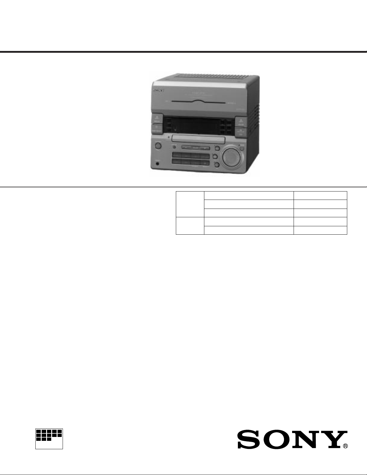
HCD-H11/H11J
SERVICE MANUAL
r
HCD-H11 is the tuner deck, CD and
amplifier section in CHC-P11.
r
HCD-H11J is the tuner deck, CD and
amplifier section in CHC-P11J.
Photo : AEP Model
Dolby noise reduction manufactured under license from
Dolby Laboratories Licensing Corporation.
“DOLBY” and the double-D symbol a are trademarks of
Dolby Laboratories Licensing Corporation.
CD player section
System Compact disc digital audio
Laser Semiconductor laser
Laser output Max 44.6µW*
Wavelength 780–790 nm
Frequency response
Signal-to-noise ratio
Dynamic range
Tuner section
FM stereo, FM/AM superheterodyne tuner
FM tuner section
Tuning range
system
(λ =780nm)
Emission duration :
continuous
*This output is the value measured at
a distance of 200 mm from the objective lens surface on the Optical
Pick-up Block with 7 mm aperture.
2Hz – 20kHz
More than 65 dB
More than 97 dB
Except East European model :
87.5 - 108.0MHz (50kHz step)
Antenna FM lead antenna
Antenna terminals
Intermediate frequency
AM tuner section
Tuning range
CD
Section
Tape deck
Section
SPECIFICATIONS
East European model :
FM1 : 65 - 74 MHz (10kHz step)
FM2 : 87.5 - 108 MHz (50kHz
75 ohm unbalanced
10.7MHz
AEP, UK, East European, German
model :
MW : 531 - 1,602kHz
LW : 153 - 279kHz
Italian model :
MW : 522 - 1,611kHz
(9kHz step)
LW : 153 - 279kHz
E3, Saudi Arabia, Hong kong,
Malaysia, Singapore, Taiwan model :
MW : 531 - 1,602kHz
(9kHz step)
530 - 1,710kHz
(10kHz step)
SW : 5.95 - 17.9kHz
AEP Model
UK Model
E Model
Austr alian Model
HCD-H11
Saudi Arabia Model
HCD-H11/H11J
Model Name Using Similar Mechanism HCD-H801
CD Mechanism Type CDM28-5BD19
Base Unit Name BU-5BD19
Model Name Using Similar Mechanism HCD-H881
Tape Transport Mechanism Type TCM- 220WR2
E2, Mexican, Argentine model :
AM : 531 - 1,710kHz (9kHz step)
AM : 530 - 1,710kHz (10kHz step)
step)
Antenna AM loop antenna
Intermediate frequency
Tape player section
Recording system
Frequency response
Wow and flutter
Amplifier section
Peak music power output
Australian model
AM : 531 - 1,602kHz (9kHz step)
AM : 530 - 1,710kHz (10kHz step)
External antenna terminals
450kHz
4-track 2-channel stereo
(DOLBY NR OFF)
40 - 13,000 Hz (±3 dB),
using Sony TYPEI cassette
40 - 14,000 Hz (±3 dB),
using Sony TYPEII cassette
0.1% WRMS ±0.3%(DIN)
400W
–Continued on Page 2–
MICROFILM
MINI Hi-Fi COMPONENT SYSTEM
Page 2

Continuous RMS power output
23W + 23W (4 ohms at
1kHz, 5% THD)
Inputs
MD IN : Sensitivity 450 mV,
impedance 47 kilohms
Outputs
MD OUT :Senitivity 250 mV, 1kΩ
PHONES (stereo phone jack) :
accept headphones of
8 ohms or more.
TABLE OF CONTENTS
Section Title Page
______ ____ ____
Specification ..................................................................................... 1
1. SERVICING NOTES ............................................................... 4
2. GENERAL
Index to Parts and Controls ........................................................ 3
Supplied accessories
AM loop antenna (1)
Remote (1)
Sony SUM-3 (NS) batteries (2)
FM lead antenna (1)
General
Destination Power requirements
Mexican model 120v AC,60Hz
AEP, UK, German,
Italian, East
European model
Australian model 240V AC, 50/60Hz
E, Saudi Arabia,
Hong Kong,
Singapore, Argentine,
Malaysia, Taiwan
model
Dimensions Approx. 225 x 210x235 mm
(w/h/d) incl. projecting
parts and controls
Mass Approx.4.8kg
Design and specifications are subject to change without notice.
220 - 230V AC, 50/60Hz
110 - 120V/ 220 - 240V
AC, 50/60Hz Adjustable
with the Voltage Selector
consumption
Power
75W
3. DISASSEMBLY
3-1. Front Panel Removal........................................................... 8
3-2. CD Mechanism, Main Board and TCB Board Removal .... 9
3-3. Mechanism Deck Removal ................................................. 9
4. ADJUSTMENTS
4-1. Mechanical Adjustment .................................................... 10
4-2. Electrical Adjustment........................................................ 10
5. EXPLANATION OF IC TERMINALS.................................. 17
6. DIAGRAMS
6-1. Block Diagram - CD Section ............................................ 21
6-2. Block Diagram - Main Section ......................................... 23
6-3. Circuit Board Location ..................................................... 27
6-4. Schematic Diagram - Main Section .................................. 28
6-5. Printed Wiring Boards - Main Section.............................. 33
6-6. Schematic Diagram - TCB Section................................... 36
(AEP,UK,G,IT,EE model)
6-7. Printed Wiring Boards - TCB Section .............................. 38
(AEP,UK,G,IT,EE model)
6-8. Printed Wiring Boards - TCB Section .............................. 39
(E3,EA,MY,SP,HK,TW,E2,MX,AR,AU model)
6-9. Schematic Diagram - TCB Section................................... 40
(E3,EA,MY,SP,HK,TW,E2,MX,AR,AU model)
6-10. Schematic Diagram - BD Section ................................... 45
6-11. Printed Wiring Boards - BD Section............................... 48
6-12. Printed Wiring Boards - Audio Section .......................... 49
6-13. Schematic Diagram - Audio Section............................... 50
6-14. Schematic Diagram - Panel Section................................ 54
6-15. Printed Wiring Boards - Panel Section ........................... 57
7. EXPLODED VIEWS
7-1. Chassis Section ................................................................. 59
7-2. Front Panel Section ........................................................... 61
7-3. TC Mechanism Section-1 ................................................. 63
7-4. TC Mechanism Section-2 ................................................. 64
7-5. CD Mechanism Section-1 ................................................. 65
7-6. CD Mechanism Section-2 ................................................. 66
8. ELECTRICAL PARTS LIST ................................................ 67
– 2 –
Page 3
SECTION 1
SERVICING NOTES
MODEL IDENTIFICATION
(Specifcation Lable)
HCD-H11
HCD-H11J
MODEL NO.
COMPACT DISC DECK RECEIVER
AEP, UK, German, Italian,
East Europian model : AC220-230V⁄50/60Hz
Australian model : AC240V⁄50Hz
Maxican model : AC120V⁄60Hz
E, Saudi Arabia, Hong Kong,
Singapore, Argentine,
Malaysia, Taiwan model: AC110-120V/220-240V⁄50/60Hz
NOTES ON HANDLING THE OPTICAL PICK-UP BLOCK
OR BASE UNIT
The laser diode in the optical pick-up block may suffer electrostatic
breakdown because of the potential difference generated by the
charged electrostatic load, etc. on clothing and the human body.
During repair, pay attention to electrostatic breakdown and also use
the procedure in the printed matter which is included in the repair
parts.
The flexible board is easily damaged and should be handled with
care.
NOTES ON LASER DIODE EMISSION CHECK
The laser beam on this model is concentrated so as to be focused on
the disc reflective surface by the objecti ve lens in the optical pick-up
block. Therefore, when checking the laser diode emission, observe
more than 30 cm away from the objective lens.
CHUCK PLATE JIG ON REPAIRING
On repairing CD section, playing a disc without the CD lid, use Chuck
Plate Jig.
r Code number of Chuck Plate Jig : X-4918-255-1
SAFETY-RELATED COMPONENT WARNING!!
COMPONENTS IDENTIFIED BY MARK ! OR DOTTED LINE
WITH MARK ! ON THE SCHEMATIC DIAGRAMS AND IN THE
PARTS LIST ARE CRITICAL TO SAFE OPERATION.
REPLACE THESE COMPONENTS WITH SONY PARTS WHOSE
PART NUMBERS APPEAR AS SHOWN IN THIS MANUAL OR IN
SUPPLEMENTS PUBLISHED BY SONY.
Laser component in this product is capable of emitting radiation
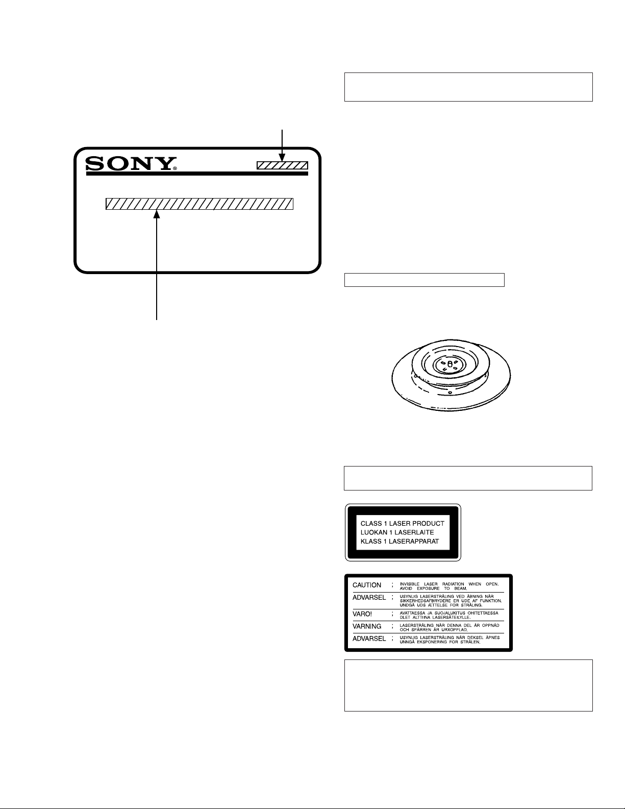
exceeding the limit for Class 1.
This appliance is classified as a
CLASS 1 LASER product. The
CLASS 1 LASER PRODUCT
MARKING is located on the
rear exterior.
This caution label
is located inside the
unit.
CAUTION
Use of controls or adjustments or performance of procedures other
than those specified herein may result in hazardous radiation
exposure.
– 3 –
Page 4
SECTION 2
GENERAL
This section is extracted from
instruction manual.
– 4 –
(E, Saudi Arabia, Argentine, Hong Kong,
Mexican, Malaysia, Singapore, Taiwan
model)
Page 5
– 5 –
Page 6
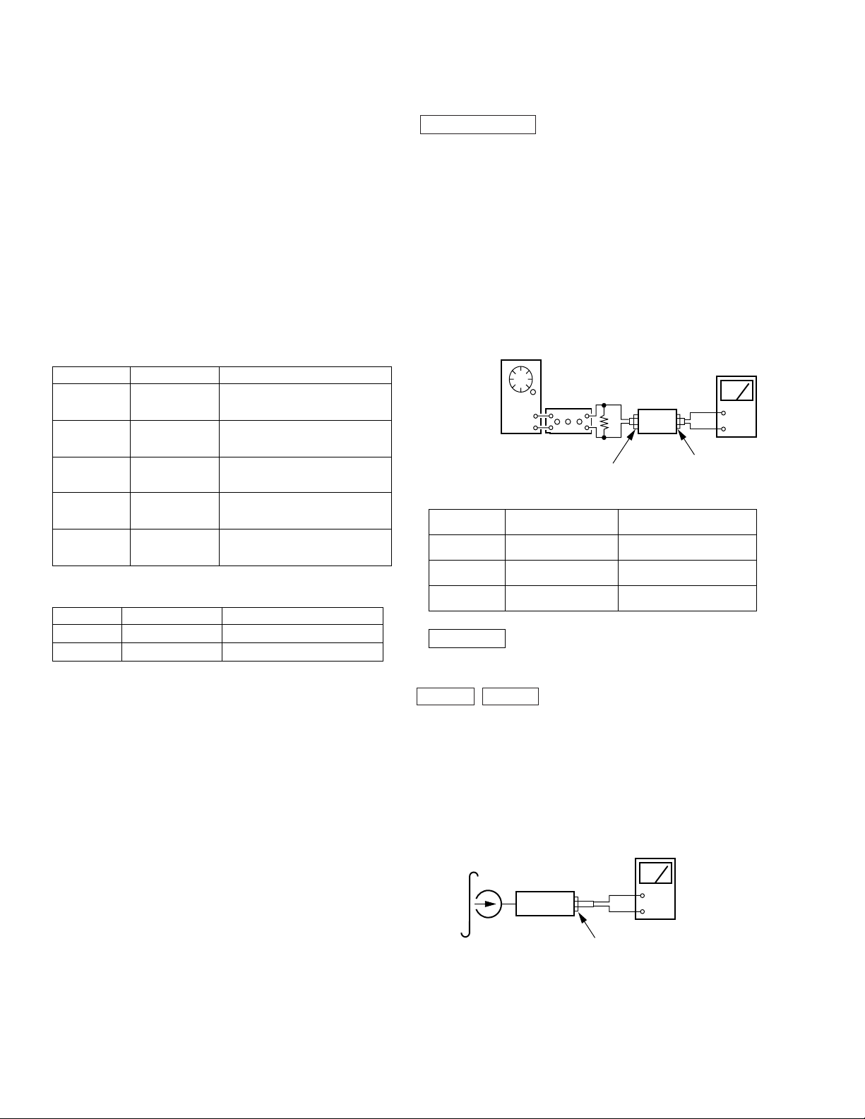
Notes for repairing CD MECHANISM section electric flow.
Two jigs (J-2501-091-A and J-2501-092-A) are necessary for the CD MECHANISM section electric flow.
Connect SET and JIG as shown in the figure below and turn the power switch on.
Jig
(J-2501-092-A)
CN101
(19 pin)
Jig
(J-2501-091-A)
CN291
(5 pin)
CNU102
(19 pin)
– 6 –
Page 7
r Disc table getting out procedure on the power supply is OFF
Disc Table
– 7 –
Page 8
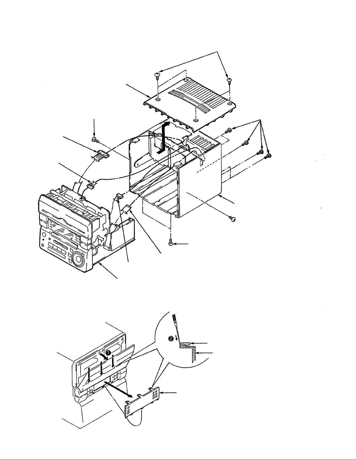
DISASSEMBLY
Note : Follow the disassembly procedure in the numerical order given.
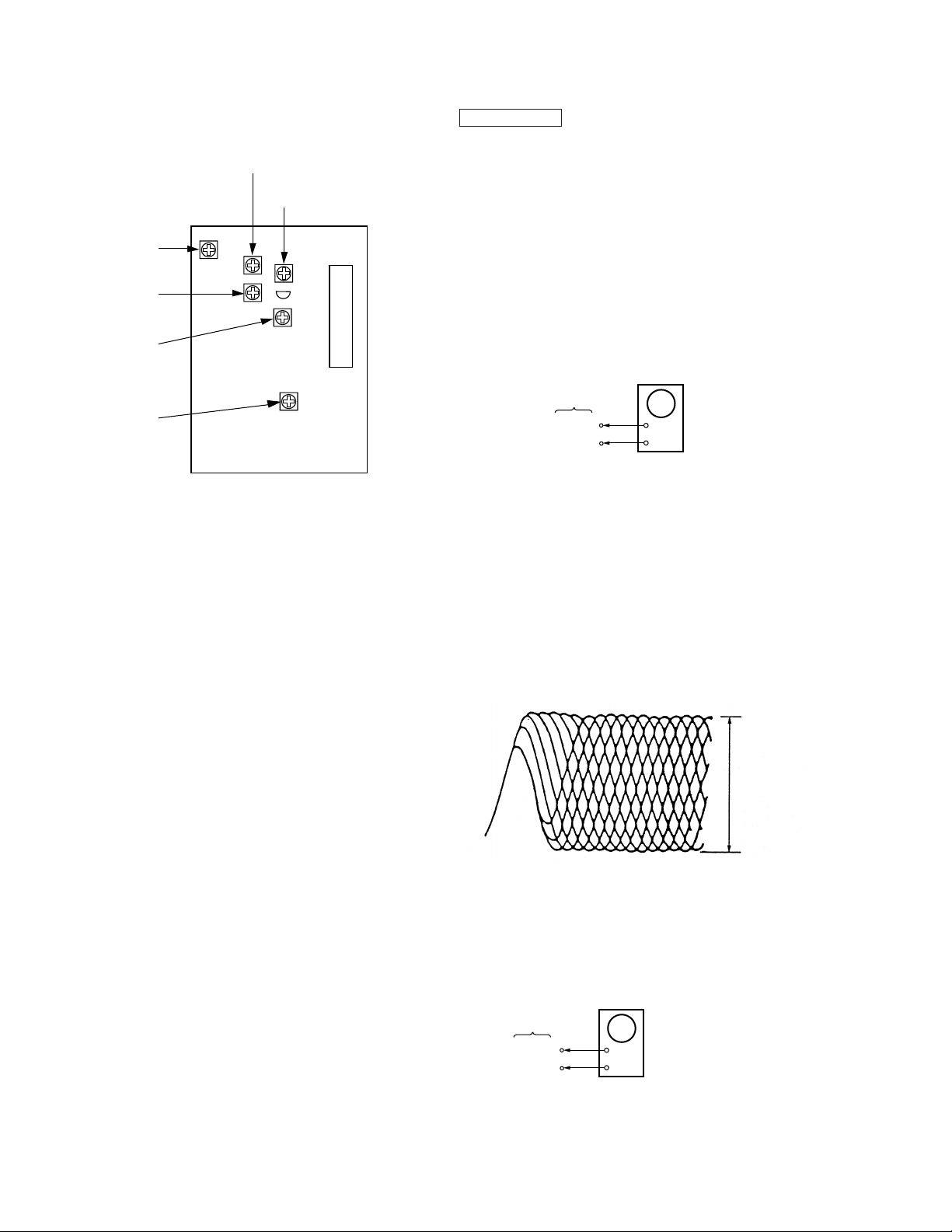
3-1. FRONT PANEL REMOVAL
4
Plate, top
2
Screw (Case 3TP2)
6
CN803
(8 pin)
7
CN602
(2 pin)
SECTION 3
3
Screw (Case 3TP2)
5
Screw (+BVTP3X10)
r
TO ADJUST THE AZIMUTH
8
CN801
(3 pin)
Front Panel Section
1
Screw (+BVTT3X6)
9
Wire (Flat Type) (17 cove)
Front Panel
Case
2
Window (DIS)
Screw (Case 3TP2)
– 8 –
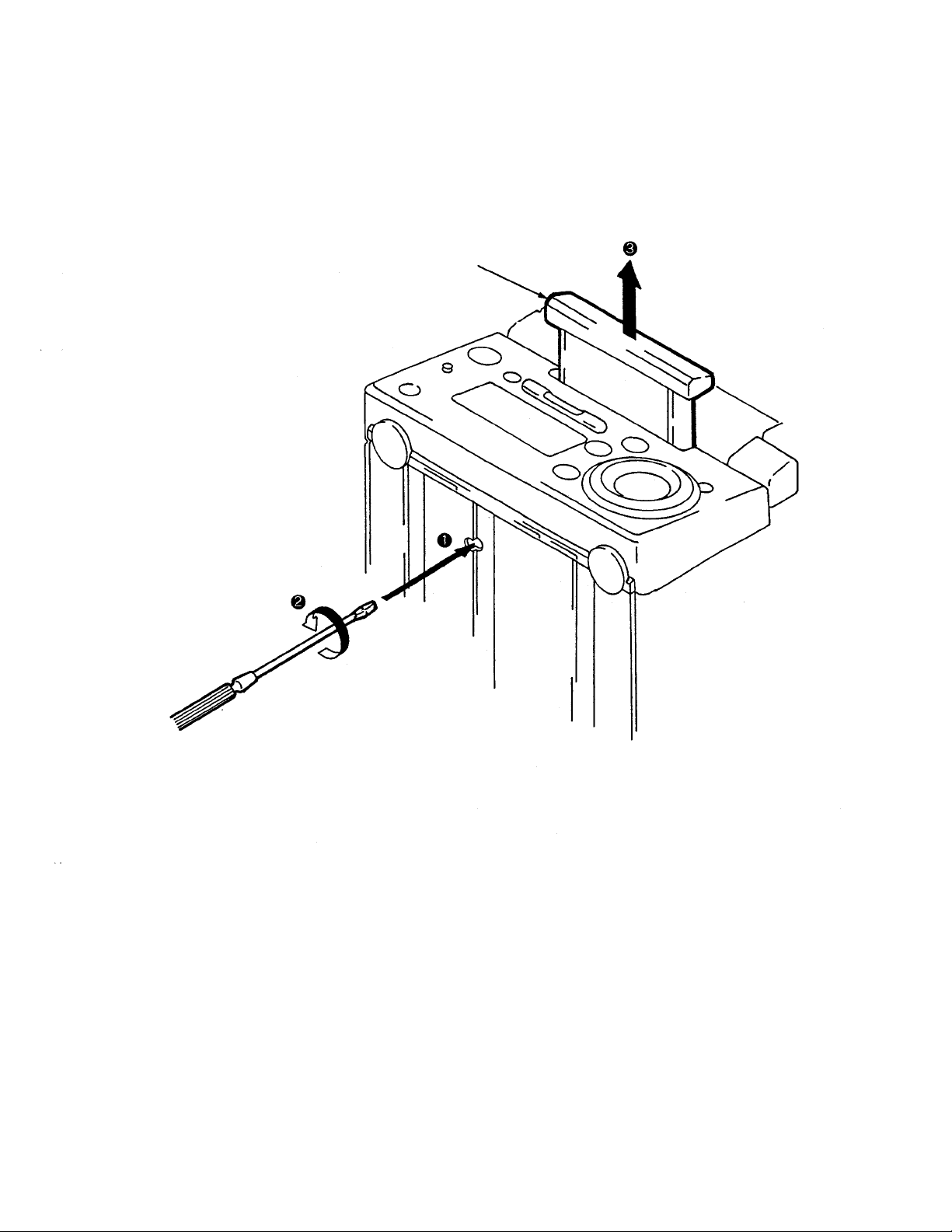
Window (DIS)
1
2
with a tool such as a thin screwdriver and
remove the window (DIS).
Raise the cassette lid.
Press on the window (DIS) clips (3 locations)
Page 9
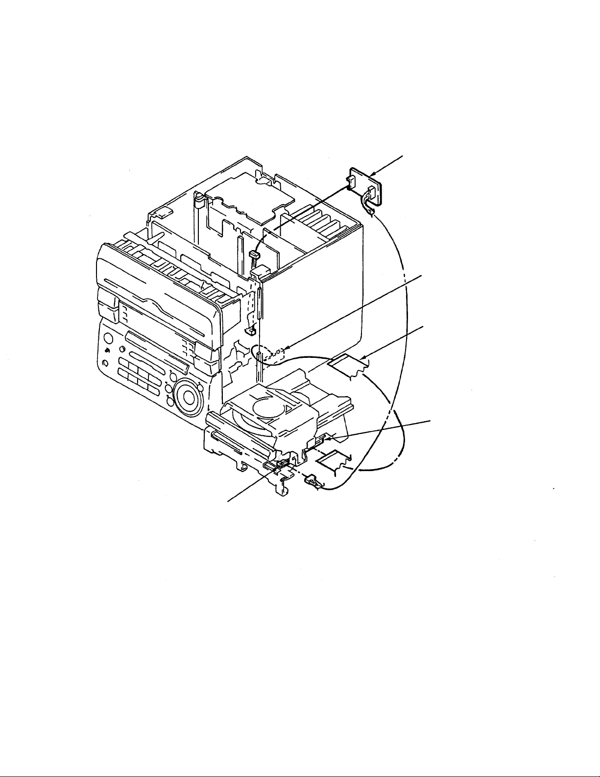
3-2. CD MECHANISM, MAIN BOARD AND TCB BOARD
7
CD MECHANISM SECTION
(CDM28-5BD19)
2
Wire (Flat Type) (11 core)
1
Wire (Flat Type) (21 core)
3
Screw (+BVTP2.6X8)
4
CN291
(5 pin)
TCB Board
(TCB017)
Main Board
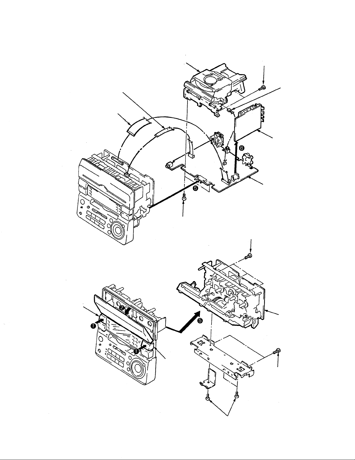
3-3. MECHANISM DECK REMOVAL
Button
(EJ-L)
Button
(EJ-R)
6
Screw (+BVTT3X6)
3
Screw (+BVTP2.6X8)
Mechanism Deck Section
(TCM-220WR2)
4
Screw (+BVTP2.6X8)
– 9 –
6
Screw (+BVTT3X6)
Page 10
set
MD OUT
Level meter
+
–
MD IN
AF OSC
attenuator
600
Ω
r
SECTION 4
ADJUSTMENTS
4-1. MECHANICAL ADJUSTMENTS
PRECAUTION
1. Clean the following parts with a denatured-alcohol-moistened
swab :
record/playback head pinch roller
erase head rubber belts
capstan
2. Demagnetize the record/playback head with a head demagnetizer.
3. Do not use a magnetized screwdriver for the adjustments.
4. After the adjustments, apply suitable locking compound to the
parts adjusted.
5. The adjustments should be performed with the rated power sup-
ply voltage unless otherwise noted.
r
T orque Measurement
Mode Torque Meter Meter Reading
Forward CQ-102C
Forward
Back Tension
Reverse CQ-102RC
Reverse
Back Tension
FF, REW CQ-201B
r
T ape Tension Measurement
Mode Torque Meter Meter Reading
Forward CQ-403A more than 100g (3.53 oz)
Reverse CQ-403R more than 100g (3.53 oz)
CQ-102C
CQ-102RC
36 to 61g•cm
(0.50 – 0.84 oz•inch)
2 to 6g•cm
(0.026 – 0.082 oz•inch)
36 to 61g•cm
(0.50 – 0.84 oz•inch)
2 to 6g•cm
(0.026 – 0.082 oz•inch)
61 to 143g•cm
(0.85 – 1.98 oz•inch)
4-2. ELECTRICAL ADJUSTMENTS
DECK SECTION
1. The adjustment should be performed in the publication.
(Be sure to make playback adjustment at first.)
2. The adjustment and measurement should be performed for
both L-CH and R-CH.
r
Switch position
DOLBY NR switch : OFF
TIMER switch : OFF
DIRECTION MODE switch : A
3. Deck section electrical adjustment are made in test mode by
pressing TUNER/BAND, DISPLAY, and FUNCTION at the
same time.
– Record Mode –
r
Test T ape
Tape Contents Use
P-4-A 100 10 kHz, –10dB Head Azimuth Adjustment
P-4-L300 315Hz, 0dB Level Adjustment
WS-48B 3kHz, 0dB Tape Speed Adjustment
0dB=0.775V
Record/Playback Head Azimuth Adjustment
DECK A DECK B
r
Setup for adjustment
When adjusting the azimuth remove, the Window (DIS) in the
center of the front panel. (Refer to page 8.)
Procedure :
1. Forward Playback mode
Reverse Playback mode
test tape
P-4-A100
(10kHz, – 10dB)
set
– 10 –
Level mete
+
-
MD OUT
Page 11
+
–
MD OUT
set
frequency counter
test tape
WS-48B
(3kHz, – 0dB)
r
2. Turn the adjustment screw for the maximum output levels. If
these levels do not match,turn the adjustment screw until both
of output levels match together within 1dB.
L-CH
peak
within
Screw
position
R-CH
peak
output
level
1 dB
within
1 dB
Tape Speed Adjustment DECK A DECK B
Procedure :
r
Perform high speed adjustment before normal speed adjustment.
Mode : Playback
L-CH
peak
R-CH
peak
screw angle
3. Playback Mode
test tape
P-4-A100
(10kHz, – 10dB)
L-CH
set
R-CH
MD OUT
screen patten
in phase 45˚ 90˚ 135˚ 180˚
good wrong
Oscilloscope
H
V
4. Change the review playback mode and repeat the steps 1 to 3.
5. After the adjustment, lock the adjustment screw with suit
able locking compound.
Adjustment Location :
– record/playback head (Deck A and B)
Dack A
Dack B
Speed Deck Adjustment Frequency counter
*High
Normal
Continus to press HIGH SPEED DUBBING switch (S507) in
*
A RV652
B RV652
A RV651
B RV651
5,970 to 6,030Hz
2,940 to 3,090Hz
playback mode : High speed palyback.
Frequency difference between the begining and the end of the tape
should be within ± 3%.
Frequency difference between deck A and deck B the biginning
of the tape should be within 1.5%.
Adjustment Location : AUDIO board.
(see page 12)
Playback Level Adjustment DECK A DECK B
Procedure :
Mode : Playback
test tape
P-4-L300
(315kHz, –10dB)
set
Level mete
+
–
MD OUT
Deck A is RV311 (L-CH) and RV411 (R-CH), deck B is RV301 (LCH) and RV401 (R-CH) so that adjustment within adjustment level
as follows.
forward
Adjustment Screw
Adjustment Level :
MD OUT level : – 3.5 ± 0.5dB (0.489 to 0.546V)
Level Difference between Channels : within 0.5dB
Confirm the OUT PUT level does not change in playback mode while
changing the mode from playback to stop several times.
Adjustment Location : AUDIO board.
(see page 12)
reverse
– 11 –
Page 12
Record Bias Adjustment DECK B
r
r
)
Procedure :
1. Record mode
AF OSC
600
attenuator
Ω
set
blank tape
CS-123
3. Confirm playback the signal recorded in step become
adjustment level as follows.
4. If these levels do not adjustment level, adjust the RV401 (L-CH)
and RV451 (R-CH) to repeat step 1 and 4.
Adjustment Level :
OUT PUT level : – 28dB ± 0.5dB (29.1 to 32.7mV)
Adjustment Location : MAIN board
Adjustment Location :
MD IN
1) 315 Hz
2) 10KHz
38.8mV (–26dB)
2. Playback mode
recorded
portion
set
Level mete
+
–
MD OUT
3. Confirm playback the signal recorded in step 1 become
adjustment level as follows.
4. If these levels do not adjustment level, adjustment the RV341
(L-CH) and RV441 (R-CH) to repeat step 1 and 4.
Adjustment level :
Playback output of 315Hz to playback output of 10kHz : – 0.5dB to
0.5dB. (– 1.3 to 1.3mV)
Adjustment Location : AUDIO board .
Record Level Adjustment DECK B
Procedure :
1. Record mode
AF OSC
attenuator
Ω
600
set
MD IN
315Hz 38.8mV (–26dB)
blank tape
CS-123
[ AUDIO BOARD ] – Component side –
RV301 : Playback Level (Deck B L-CH)
RV651 : Tape Speed (Normal)
RV401 : Playback Level
(Deck B R-CH)
RV341 : Record Bias (L-CH)
RV441 : Record Bias (R-CH)
RV411 : Playback Level
(Deck A R-CH)
[ MAIN BOARD ] – Component side –
RV451 :
Record Level (R)
RV652 : Tape Speed
(HIGH)
RV311 : Playback Level
(Deck A L-CH)
RV401 :
Record Level (L
2. Playback mode
recorded
portion
set
MD OUT
Level mete
+
–
– 12 –
Page 13
TUNER SECTION
r
Precautions in Repairing
Note. 1 : The adjustment should be performed in the publication.
(MW n FM n SW)
Note. 2 : As a front-end (FE1) is dif ficult to repair if f aulty , replace it
with new one.
r
Abbreviation
AUS : Australian IT : Italian
G : German AR : Argentine
EA : Saudi Arabia HK : Hong Kong
MX : Mexican. SP : Singapore
MY : Malaysia TW : Taiwan
EE : East European
E2 : Tuner sections SW BAND do not exist.
E3 : Tuner sections SW BAND exist.
MW Tuned Indication Lighting Level
Setting :
Band : MW
loop antenna B
loop antenna A
AM RF signal
generator
Procedure :
1. Tune the set to 98MHz.
2. Adjust RV42 so that the TUNED indicator goes on.
Adjustment Location : TCB board (see page 14)
SW Control Voltage Adjustment
(Frequency Coverge Adjustment)
(E3,EA,MY,SP,HK,TW model)
Setting :
Band : SW
Procedure :
1. Connect digital Voltmeter to diode D1 center lead and ground.
2. Adjust for a following value reading on digital Voltmeter.
SW
Set frequency
5.95MHz T2 1.2Vdc
17.9MHz CV2 8.5Vdc
Adjustment
part
Reading on digital
voltmeter
Adjustment Location : TCB board (see page 14)
SW T racking Adjustment
(E3,EA,MY,SP,HK,TW model)
Setting :
Band : SW
set
Carrier frequency : 999kHz (at
Modulation : 400Hz 30% modulation
1,050kHz (at
9kHz step) or
10kHz step)
Procedure :
1. Set loop antenna A so that the loop antenna B input le vel becomes
55dBµ/m (0.6mV/m)
2. Tune the set to 999kHz (at 9kHz step) or 1,050kHz (at 10kHz
step).
3. Adjust RV41 so that the TUNED indicatior goes on.
Adjustment Location : TCB board (see page 14)
FM Tuned Indication Lighting Level
Note : Always make the tuning level adjustment first.
(Since it affects the FM tuning level.)
Setting :
Band : FW
FM RF stereo signal
generator
75
FM ANTENNA terminal
Ω
coaxial
AM RF signal
generator
Modulation : 400Hz
30% modulation
set
SPEAKER terminal
AM ANTENNA terminal
Level mete
+
–
Procedure :
Adjust for maximum reading on Level mater.
Set frequency
SW
r
Repeat the procedures is each adjustment several times, and the
7MHz T1
17MHz CV1
Adjustment
part
frequency coverage and tracking adjustment should be f inally done
by the trimmer capacitors.
Adjustment Location : TCB board (see page 14)
Carrier frequency : 98MHz
Modulation : 1kHz, 75kHz (100%)
Output level : 0.018mV (25dB )
µ
set
– 13 –
Page 14
s
Adjustment Location
[TCB BOARD] – Conductor side –
CV1 : SW Tracking Adjustment
RV41 :
MW Tuned indication
Lighting Level
T1 : SW Tracking Adjustment
CD SECTION
Note :
1. CD Block basically constructed to operate without adjustment.
Therefore, check each item in order given.
2. Use YEDS-18 disc (3-702-101-01) unless otherwise indicated.
3. Use the oscilloscope with more than 10MΩ impedance.
4. Clean an object lens by an applicator with neutral detergent when
the signal level is low than specified value with the following
checks.
CV2 :
SW Control Voltage
Adjustment
T2 :
SW Control Voltage
Adjustment
RV42 :
FW Tuned indication
Lighting Level
D1
FE1
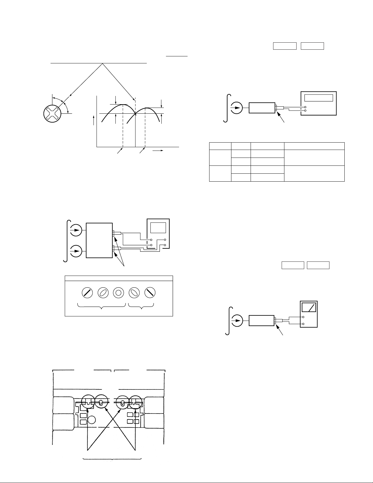
Focus Bias Adjustment
This adjustment is to be done when the optical block is replaced.
Adjustment procedure :
oscilloscope
(DC range)
BD board
TP (RF)
TP (VC)
+
–
1. Connect oscilloscope to test point TP (VC) and TP (RF) on BD
board.
2. Ground main board IC101 (pin(£) with the lead wire.
3. Turned power switch ON. (Stop mode)
4. Put disc (YEDS-18) in and press the ( button.
5. Press the P button. (Tracking servo ON)
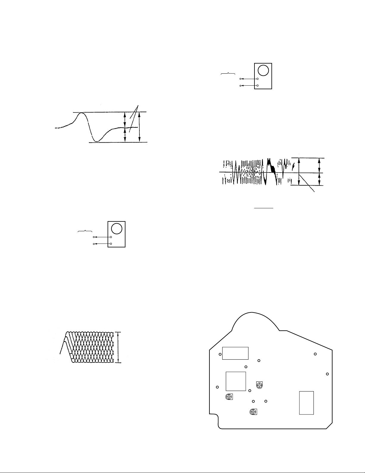
6. Adjust RV101 so that the oscilloscope waveform is as shown in
the figure below (eye pattern).
A good eye pattern means that the diamond shape (◊) in the center
of the waveform can be clearly distinguished.
7. After adjustment, remove the lead wire connecd in step 2.
r
RF signal reference waveform (eye pattern)
VOLT/DIV : 0.2V
TIME/DIV : 500n
1.3 ± 0.3Vp-p
When observing the eye pattern, set the oscilloscope for A C range
and raise vertical sensitivity.
Adjustment Location : BD board. (see page 15)
S-Curve Check
oscilloscope
BD board
TP (FEO)
TP (VC)
Procedure :
+
–
1. Connect oscilloscope to test point TP (FEO) and BD board.
2. Connect between test point TP (FOK) and TP (GND) by lead wire.
3. Turned Power switch on.
– 14 –
Page 15
4. Put disc (YEDS-18) in and turned Power switch on again and
+
–
oscilloscope
(DC range)
TP (TEO)
TP (VC)
BD board
IC102
FEI
TEI
FOK
IC101
RF
RV101
RV102
IC104
FEO
TEO
VC
PCK
GND
RV103
actuate the focus search. (actuate the focus search when disc table
is moving in and out.)
5. Check the oscilloscope waveform (S-curve) is symmetrical
between A and B. And confirm peak to peak level within
2.4±0.7Vp-p.
E-F Balance Check
S-curve waveform
symmetry
A
within 2.4
B
±
0.7Vp-p
6. After check, remove the lead wire connected in step 2.
r
Note :
Try to measure several times to make sure that the ratio of
A : B or B : A is more than 10 : 7.
r
T ake sweep time as long as possible and light up the brigh-
ness to obtain best waveform.
Adjustment Location : BD board. (see page 15)
RF Level Check
oscilloscope
BD board
TP (RF)
TP (VC)
+
–
Procedure :
1. Connect oscilloscope to test point TP (RF) on BD board.
2. Turned Power switch on.
3. Put disc (YEDS-18) in and press the ( button.
4. Confirm that oscilloscope wav eform is clear and check RF signal
level is correct or not.
Note :
Clear RF signal waveform means that the shape “ ◊ ” can be clearly
distinguished at the center of the waveform.
Procedure :
1. Ground main board IC101 (pin (£) with the lead wire.
2. Connect oscilloscope to test point TP (TEO) on BD board.
3. Turned Power switch on.
4. Put disc (YEDS-18) in and press the ( button.
5. Confirm that the osilloscope waveform is symmetrical on the
top and bottom in relation to 0V, and check this level.
Traverse waveform
A
0V
B
level : 300 ± 100mVp-p
specified value : r
A–B
2 (A+B)
r
A+B = 300 ± 100mVp-p
X100 = less than ± 7%
6. Remove the lead wire connected in step 1.
Focus/Tracking Gain Adjustment (RV102, RV103)
This gain has a margin, so even if it is slightly off. There is no problem.
Therefore, do not perform, this adjustment.
Please note that it should be fixed to mechanical center position when
you moved and do not know original position.
Adjustment Location :
[BD BOARD] – Conductor side –
RF signal waveform
VOLT/DIV : 200mV
TIME/DIV : 500ns
level : 1.3
Adjustment Location : BD board. (see page 15)
±
0.3Vp-p
– 15 –
Page 16
SECTION 5
EXPLANATION OF IC TERMINALS
IC101 TMP87CP64YF - 6335 (MASTER CONTROL)
Pin No. Pin name I/O Description
1VSS – Ground
2 X OUT O
––––––––––––––––––––––––––––––––––––––––––––––––––––––––––––––––––––––––––––––––––––––––––––
3 X IN I
4
5 X OUT O
––––––––––––––––––––––––––––––––––––––––––––––––––––––––––––––––––––––––––––––––––––––––––––
–––––––––––––––
RESET
6 X IN I
7 GND – Ground.
8
–––––––––––––––––––
BACK UP
9 COUNT SW – Not used. (Ground)
10 INIT SW – Not used. (Ground)
11
12
13
14
15
16
DISC SENS
MID SENS
CD XRST
POWER
MUTE
MPX
17 KEYCON LATCH – Not used. (Open)
18
VOL LATCH O
19 ST MUTE – Not used. (Open)
20
ST FM
21 FUNC A O
––––––––––––––––––––––––––––––––––––––––––––––––––––––––––––––––––––––––––––––––––––––––––––
22 FUNC B O
––––––––––––––––––––––––––––––––––––––––––––––––––––––––––––––––––––––––––––––––––––––––––––
23 FUNC C O
Main system clock. (10MHz)
I Reset signal input terminal.
Sub system clock.(32kHz).
I BACK-UP mode input terminal.
– Not used. (Ground)
– Not used. (Ground)
O CD Reset output. “L” : RESET
O Power on output. “L” : ON
O Mute output. “L” : MUTE
– Not used. (Open)
Latch output to volume control. (TC9210P)
– Not used. (Open)
FUNCTION FUNC A FUNC B FUNC C
ST L L H
CD L H H
Function Select.
TC H L H
MDHH L
24 GEQ.LATCH O Latch output to gray control. (M6243FP)
25 RDS. INT I Not used. (+5V)
26 SCOR (DSP) I Sub code sync SO+SI detection input from DSP. (CXD2507AQ)
27 CIN / SENS I SENS input from DSP. (CXD2507AQ)
28 CD POWER O Power on output. “H” : ON
29 CDG LATCH – Not used. (Open)
30 DBFB- 2 – Not used. (Open)
31
32
33
34
MUTE
CE
STEREO
TUNED
– Not used. (Open)
O Chip enable output to tuner PLL IC. (LC72130)
I FM/AM Stereo identification. “L” : STEREO
I FM/AM Tuning identification. “L” : TUNING
35 SQ-RDS-CLK O Sub-code Q data scanning clock output to DSP (CXD2507AQ), RDS clock output.
36 SQ-RDS-DI I Sub-code Q data input from DSP (CXD2507AQ), RDS data input.
37 RDS-RESET – Not used. (Open)
38 CLK O System clock output.
39
D. IN
I Serial data input from tuner.
40 D. OUT O Serial data (COMN) output.
– 16 –
Page 17

Pin No. Pin name I/O Description
41 CDG MUTE – Not used. (Open)
42 REQ GM I Data transmission request input from system control.
43 MREQ O Not used. (+5V)
44 CLK MG O Clock output for communications with system control.
45 D. GM I Serial data input from system control.
46 D. MG O Serial data output to system control.
47 RDY I/O System control Ready signal input / output. “L” : READY
48 VAREF – Power supply. (+5V)
49 VASS – Ground
50 VSS – Ground
51 VDD – Power supply. (+5V)
52 URGENT. SIG I Not used. (+5V)
53 URGENT. STBY I Not used. (Open)
54 BUG Y/N – Not used. (Ground Connected)
–––
55 ADJUSTOR – Not used. (“H” LEVEL)
56 ADJUST2 – Not used. (“H” LEVEL)
57 MAGIC SPEED – Not used. (“H” LEVEL)
58 SPEC I Not used. (“H” LEVEL)
59 DIST I Model Select input . (A/D Converter)
60 SPEED – Not used. (“H” LEVEL)
61 BREAK – Not used. (“H” LEVEL)
62 B-PLAY I Deck-B PLAY Switch input. “H” : PLAY
63 B-SHUT I Deck-B Reel table signal input.
64 B-HALF I Deck-B Record prevention claw A, B detection input.
65 A-SHUT I Deck-A Reel table signal input.
66 A-PLAY I Deck-A PLAY Switch input. “H” : PLAY
67
A-HALF
I Deck-A HALF SW input.
68 CAPM H/L O Capstan motor speed selector. “H” : Normal speed “L” : High speed
69
70
––––––––––––––––––––––––––––––––––––––––––––––––––––––––––––––––––––––––––––––––––––––––––––
71 B TRG O Trigger motor control output.
––––––––––––––––––––––––––––––––––––––––––––––––––––––––––––––––––––––––––––––––––––––––––––
CAPM ON/OFF
TRIG H/L
O Capstan motor ON/OFF. “L” : ON
O
72 A TRG O
73 RELAY O Control output to REC/PB select switch. (IC602)
74 A/B O Dolby IC PB input Deck A/B select output. “L” : A, “H” : B
75 NORM/HIGH O EQ Select switch output for normal / high speed. “H” : High speed
76 BIAS ON/OFF O BIAS Oscillation ON/OFF control. “H” : ON
77 RM ON/OFF O REC Mute output. “L” : MUTE
78
79
80
81
REC/PB
NR
LM
PASS
O DOLBY IC REC/PLAY Select output. “H” : REC
O DOLBY ON/OFF Control output. “H” : ON
O LINE Mute output. “L” : MUTE
O PASS Amplifier switch output to DOLBY IC. (IC401)
82 CMD2 – Not used. (Open)
83 UP MOTOR – Not used. (Open)
84 DOWN MOTOR – Not used. (Open)
85 TABLE R – Not used. (Open)
– 17 –
Page 18

Pin No. Pin name I/O Description
86 TABLE L – Not used. (Open)
87 LOAD OUT O Loading motor (M903) Load out output.
88 LOAD IN O Loading motor (M903) Load in output.
89 DF-LATCH O Latch output to digital filter. (PCM1701U)
90 XLT O Serial data latch output to DSP. (CDX2507AQ)
91 FOCUS SW O High-region gain down output to focus servo. (CXA1782BQ)
92 HIGH DUBB – Not used. (“H” LEVEL)
93 TEST 1 – Not used. (“H” LEVEL)
94 OUT SW I CD Tray output detection input.
95 IN SW I CD Tray input detection terminal.
96 UP SW – Not used. (Ground)
97 PANEL SW – Not used. (Ground)
98 CLOSE SW – Not used. (Ground)
99 OPEN SW – Not used. (Ground)
100 VDD – Power supply. (+5V)
– 18 –
Page 19

IC501 CXP82612-016Q (SYSTEM CONTROL DRIVE)
Pin No. Pin name I/O Description
1 ENC I Volume encoder input terminal.
2 SIRCS I Remote commander signal input.
3 REQ. MG I Data transmission request input from master control.
4 REQ. GM O Data transmission request output to master control.
5 LED1 O LED DRIVE Output.
6 LED2 – Not used. (Open)
7 LED3 – Not used. (Open)
8 LED4 – Not used. (Open)
9 LED5 O PLAY, PAUSE LED Output.
10 RDY I/O Master control Ready signal input / output. “L” : Ready
11 SCK. IN I Clock output for communications with master control.
12 SD. IN I Serial data input from master control.
13 SD. OUT O Serial data output to master control.
14 LED-PAUSE O REC, PAUSE LED Output.
15 LED-CD O ROCK LED Output.
16 LED-TUNER/BAND O JAZZ, DRECTION MODE LED Output
17 LED-TAPE O CLASSIC, DANCE LED Output.
18 LED-FWD,STOP,FF&REW O TUNER LED Output.
19 LED-DECK A/B & REV O CD, TIMER LED Output.
20 LED-A O ENTER / NEXT, TUNER / BAND LED Output.
21 LED-B O A, B LED Output.
22 KEY1 I
––––––––––––––––––––––––––––––––––––––––––––––––––––––––––––––––––––––––––––––––––––––––––––
23 KEY2 I
––––––––––––––––––––––––––––––––––––––––––––––––––––––––––––––––––––––––––––––––––––––––––––
24 KEY3 I
––––––––––––––––––––––––––––––––––––––––––––––––––––––––––––––––––––––––––––––––––––––––––––
Key input. (A/D Converter)
25 KEY4 I
26 PBF1 I
––––––––––––––––––––––––––––––––––––––––––––––––––––––––––––––––––––––––––––––––––––––––––––
27 PBF2 I
––––––––––––––––––––––––––––––––––––––––––––––––––––––––––––––––––––––––––––––––––––––––––––
28 PBF3 I
––––––––––––––––––––––––––––––––––––––––––––––––––––––––––––––––––––––––––––––––––––––––––––
Not used. (Ground)
29 PBF4 I
30 RST I Reset signal input terminal.
31 X IN I
––––––––––––––––––––––––––––––––––––––––––––––––––––––––––––––––––––––––––––––––––––––––––––
32 X OUT O
––––
system clock. (4MHz)
33 VSS – Gound
34 P29 O
––––––––––––––––––––––––––––––––––––––––––––––––––––––––––––––––––––––––––––––––––––––––––––
35 P28 O
––––––––––––––––––––––––––––––––––––––––––––––––––––––––––––––––––––––––––––––––––––––––––––
36 P27 O
––––––––––––––––––––––––––––––––––––––––––––––––––––––––––––––––––––––––––––––––––––––––––––
37 P26 O
––––––––––––––––––––––––––––––––––––––––––––––––––––––––––––––––––––––––––––––––––––––––––––
38 P25 O
––––––––––––––––––––––––––––––––––––––––––––––––––––––––––––––––––––––––––––––––––––––––––––
39 P24 O LED Drive.
––––––––––––––––––––––––––––––––––––––––––––––––––––––––––––––––––––––––––––––––––––––––––––
40 P23 O
––––––––––––––––––––––––––––––––––––––––––––––––––––––––––––––––––––––––––––––––––––––––––––
41 P22 O
––––––––––––––––––––––––––––––––––––––––––––––––––––––––––––––––––––––––––––––––––––––––––––
42 P21 O
––––––––––––––––––––––––––––––––––––––––––––––––––––––––––––––––––––––––––––––––––––––––––––
43 P20 O
––––––––––––––––––––––––––––––––––––––––––––––––––––––––––––––––––––––––––––––––––––––––––––
44 P19 O
– 19 –
Page 20

Pin No. Pin name I/O Description
45 P18 O
––––––––––––––––––––––––––––––––––––––––––––––––––––––––––––––––––––––––––––––––––––––––––––
46 P17 O
––––––––––––––––––––––––––––––––––––––––––––––––––––––––––––––––––––––––––––––––––––––––––––
47 P16 O
––––––––––––––––––––––––––––––––––––––––––––––––––––––––––––––––––––––––––––––––––––––––––––
48 P15 O
––––––––––––––––––––––––––––––––––––––––––––––––––––––––––––––––––––––––––––––––––––––––––––
49 P14 O
––––––––––––––––––––––––––––––––––––––––––––––––––––––––––––––––––––––––––––––––––––––––––––
50 P13 O
––––––––––––––––––––––––––––––––––––––––––––––––––––––––––––––––––––––––––––––––––––––––––––
51 P12 O
––––––––––––––––––––––––––––––––––––––––––––––––––––––––––––––––––––––––––––––––––––––––––––
52 P11 O
––––––––––––––––––––––––––––––––––––––––––––––––––––––––––––––––––––––––––––––––––––––––––––
53 P10 O
––––––––––––––––––––––––––––––––––––––––––––––––––––––––––––––––––––––––––––––––––––––––––––
54 P9 O
––––––––––––––––––––––––––––––––––––––––––––––––––––––––––––––––––––––––––––––––––––––––––––
55 P8 O
––––––––––––––––––––––––––––––––––––––––––––––––––––––––––––––––––––––––––––––––––––––––––––
56 P7 O
––––––––––––––––––––––––––––––––––––––––––––––––––––––––––––––––––––––––––––––––––––––––––––
57 P6 O LED Drive.
––––––––––––––––––––––––––––––––––––––––––––––––––––––––––––––––––––––––––––––––––––––––––––
58 P5 O
––––––––––––––––––––––––––––––––––––––––––––––––––––––––––––––––––––––––––––––––––––––––––––
59 P4 O
––––––––––––––––––––––––––––––––––––––––––––––––––––––––––––––––––––––––––––––––––––––––––––
60 P3 O
––––––––––––––––––––––––––––––––––––––––––––––––––––––––––––––––––––––––––––––––––––––––––––
61 P2 O
––––––––––––––––––––––––––––––––––––––––––––––––––––––––––––––––––––––––––––––––––––––––––––
62 P1 O
––––––––––––––––––––––––––––––––––––––––––––––––––––––––––––––––––––––––––––––––––––––––––––
63 7G O
––––––––––––––––––––––––––––––––––––––––––––––––––––––––––––––––––––––––––––––––––––––––––––
64 6G O
––––––––––––––––––––––––––––––––––––––––––––––––––––––––––––––––––––––––––––––––––––––––––––
65 5G O
––––––––––––––––––––––––––––––––––––––––––––––––––––––––––––––––––––––––––––––––––––––––––––
66 4G O
––––––––––––––––––––––––––––––––––––––––––––––––––––––––––––––––––––––––––––––––––––––––––––
67 3G O
––––––––––––––––––––––––––––––––––––––––––––––––––––––––––––––––––––––––––––––––––––––––––––
68 2G O
––––––––––––––––––––––––––––––––––––––––––––––––––––––––––––––––––––––––––––––––––––––––––––
69 1G O
70 NC – Not used. (Open)
71 VFDP – LED Drive – 25V power supply.
72 VDD – Power supply. (+5V)
73 KEY – Not used. (+5V)
74 KEY – Not used. (+5V)
75 VDD (TEST) – Not used. (+5V)
76 LED-TUNER-COMMON O Forward play, Revers play LED output.
77 LED-ENTER-NEXT O ENTER / NEXT LED Output.
78 ENC B I
––––––––––––––––––––––––––––––––––––––––––––––––––––––––––––––––––––––––––––––––––––––––––––
79 ENC A I
AMS ENCODER input terminal.
80 ENC – Not used. (+5V)
– 20 –
Page 21

Page 22

Page 23

Page 24

Page 25

Page 26

Page 27

Page 28

Page 29

Page 30

SECTION 7
EXPLODED VIEWS
NOTE :
r
-XX, -X mean standardized parts, so they may
have some difference from the original one.
r
Items marked “ * ”are not stocked since they
are seldom required for routine service. Some
delay should be anticipated when ordering these
items.
7-1.CABINET SECTION
2
3
r
The mechanical parts with no reference number
in the exploded views are not supplied.
r
Hardware (# mark) list and accessories and
packing materials are given in the last of this
parts list.
r
Abbreviation
SP : Singapore AUS : Australian
HK : Hong Kong AR : Argentine MX : Mexican
G : German EA : Saudi Arabia IT : Italian
MY : Malaysia EE : East European TW : Taiwan
E2 : Tuner Sections SW BAND do not exist.
E3 : Tuner Sections SW BAND exist.
S801
4
F801
#2
2
AR, TW, SP, MY,
5
MX, HK, E, EA
T801
7
F802
#3
4
IC801
14
15
16
#3
10
not supplied
The components identified by mark
! or dotted line with mark ! are
critical for safety.
Replace only with part number
specified.
not supplied
not supplied
IC901
6
#3
#4
#1
#1
8
#3
Q804
14
E3 model
11
E,MX model
9
not supplied
2
#1
#1
#1
1
2
#1
AEP, G, IT,EA,EE
9
AUS model
AED, AR, HK,
MY, SP, TW model
9
UK model
12
13
EA, MY, SP, TW model
9
HK model
– 59 –
Page 31

Ref. No. Part No. Description Remark Ref. No. Part No. Description Remark
––––––– ––––––– –––––––––– ––––––– ––––––– ––––––– –––––––––– ––––––
* 1 4-977-369-21 CASE (H11 : AEP,UK,G,IT,EE,AUS)
1 4-977-369-31 CASE (H11 : E,EA,AR,HK,MX,MY,SP,TW,TH)
* 1 4-977-369-51 CASE (H11J)
2 3-363-099-01 SCREW (CASE 3 TP2)
3 4-977-370-11 PLATE, TOP (H11)
3 4-977-370-31 PLATE, TOP (H11J)
4 1-533-217-31 HOLDER, FUSE
* 5 1-658-263-13 TRANSFORMER BOARD
* 6 3-309-144-21 HEAT SINK
* 7 A-4389-315-A POWER BOARD, COMPLETE (H11 : AEP,UK,G,
IT,E,EA, EE,AR,AUS,HK,TW)
* 10 A-4389-314-A POWER AMP BOARD, COMPLETE (H11 : AEP,
UK,G,IT, E,EA,EE,AR,AUS,HK,TW)
* 10 A-4389-402-A POWER AMP BOARD, COMPLETE (H11 : MX)
* 10 A-4389-409-A POWER AMP BOARD, COMPLETE (H11 : MY,SP)
* 10 A-4389-474-A POWER AMP BOARD, COMPLETE (H11J)
11 1-569-007-11 ADAPTER, CONVERSION 2P (E3)
12 1-569-008-11 ADAPTER, CONVERSION 2P (EA,MY,SP,TW)
13 1-770-019-11 ADAPTOR, CONVERSION PLUG 3P (HK)
* 14 3-923-762-11 HOLDER (TR)
15 4-980-402-01 SHEET (T) (H11J)
16 4-979-267-01 SCREW (3X16) (P) (TIGHT), +BV
* 7 A-4389-403-A POWER BOARD, COMPLETE (H11 : MX)
* 7 A-4389-410-A POWER BOARD, COMPLETE (H11 : MY,SP)
* 7 A-4389-475-A POWER BOARD, COMPLETE (H11J)
8 3-703-244-11 BUSHING (2104), CORD (EXCEPT E,MX)
8 3-703-571-00 BUSHING (S) (4516), CORD (E,MX)
! 9 1-558-943-41 CORD, POWER (E,MX)
! 9 1-575-651-21 CORD, POWER (AEP,G,IT,EA,EE,AR,HK,MY,SP,
! 9 1-696-845-11 CORD, POWER (AUS)
! 9 1-751-522-11 CORD, POWER (UK)
! F801 1-532-279-00 FUSE, TIME LAG (T0.5AL/250V)
! F802 1-532-078-00 FUSE, TIME LAG (T1.0AL/250V) (E,EA,AR,HK,
IC801 8-759-231-58 IC TA7812S
IC901 8-749-920-19 IC STK4122MK2
! T801 1-429-450-11 TRANSFORMER, POWER (AEP,G,IT,EE,TH,UK)
! T801 1-429-451-11 TRANSFORMER, POWER (E,EA,AR,AUS,HK,MX,
TW)
! S801 1-572-675-11 SWITCH, POWER VOLTAGE CHANGE
(VOLTAGE SELECTOR) (E,EA,AR,HK,MX,MY,SP,TW)
The components identified by mark
! or dotted line with mark ! are
critical for safety.
Replace only with part number
specified.
MX, MY,SP,TW)
MY,SP,TW)
– 60 –
Page 32

7-2.FRONT PANEL SECTION
79
56
81
59
62
61
57
64
63
60
not
supplied
58
(including 51)
68
#5
#5
not
supplied
65
66
not
supplied
64
69
FL501
65
73
67
72
65
not
supplied
#5
70
71
not supplied
65
65
75
74
77
76
55
54
53
52
supplied with
S503
51
80
#5
78
– 61 –
Page 33

Ref. No. Part No. Description Remark Ref. No. Part No. Description Remark
––––––– ––––––– –––––––––– ––––––– ––––––– ––––––– –––––––––– ––––––
51 4-930-336-91 FOOT (FELT)
52 4-977-402-11 KNOB (JOG) (H11)
52 4-977-402-31 KNOB (JOG) (H11J)
53 4-977-383-11 BUTTON (O/C) (H11)
53 4-977-383-31 BUTTON (O/C) (H11J)
54 4-977-398-11 BUTTON (EJ-R) (H11)
54 4-977-398-31 BUTTON (EJ-R) (H11J)
55 4-977-396-01 WINDOW (DIS) (H11J)
55 4-977-396-11 WINDOW (DIS) (H11)
56 4-977-382-11 BUTTON (TIM) (H11)
56 4-977-382-31 BUTTON (TIM) (H11J)
57 4-977-397-11 BUTTON (EJ-L) (H11)
57 4-977-397-31 BUTTON (EJ-L) (H11J)
58 X-4946-766-1 PANEL (W) ASSY, FRONT (H11)
58 X-4946-817-1 PANEL (BJ) ASSY, FRONT (H11J)
59 X-4946-767-1 LID (W) ASSY, CASSETTE (H11)
59 X-4946-818-1 LID (BJ) ASSY, CASSETTE (H11J)
60 4-959-232-01 SPRING (R), TORSION (H11J)
60 4-959-232-11 SPRING (R), TORSION (H11)
61 4-959-231-01 SPRING (L), TORSION (H11J)
61 4-959-231-11 SPRING (L), TORSION (H11)
62 X-4946-761-1 HOLDER (L) ASSY, CASSETTE (H11)
62 X-4946-820-1 HOLDER (BL) ASSY, CASSETTE (H11J)
* 63 3-367-709-01 LEVER (LOCK LEVER L) (H11J)
63 3-367-709-21 LEVER (LOCK LEVER L) (H11)
64 3-354-957-01 JOINT (LOCK LEVER)
65 4-951-620-01 SCREW (2.6X8), +BVTP
66 4-965-877-01 LEVER (LOCK LEVER R) (H11J)
* 66 4-965-877-11 LEVER (LOCK LEVER R) (H11)
* 67 4-977-399-01 HOUSE, LAMP (H11J)
* 67 4-977-399-11 HOUSE, LAMP (H11)
68 X-4946-760-1 HOLDER (R) ASSY, CASSETTE (H11)
68 X-4946-819-1 HOLDER (BR) ASSY, CASSETTE (H11J)
* 69 4-977-400-01 HOLDER (FL) (H11J)
* 69 4-977-400-11 HOLDER (FL) (H11)
70 4-977-401-11 PANEL, LOADING (H11)
70 4-977-401-31 PANEL, LOADING (H11J)
71 1-776-220-11 WIRE (FLAT TYPE) (19 CORE) (H11J)
71 1-777-061-11 WIRE (FLAT TYPE) (19 CORE) (H11)
* 72 A-4389-325-A PANEL BOARD, COMPLETE (H11 : AEP,UK,G,IT,
E3,EA, EE,HK,TW)
* 72 A-4389-398-A PANEL BOARD, COMPLETE (H11 : E2,AR,AUS)
* 72 A-4389-401-A PANEL BOARD, COMPLETE (H11 : MX)
* 72 A-4389-408-A PANEL BOARD, COMPLETE (H11 : MY,SP)
* 72 A-4389-473-A PANEL BOARD, COMPLETE (H11J)
73 4-977-392-01 SPRING (F), TENSION (H11J)
73 4-977-392-11 SPRING (F), TENSION (H11)
74 1-769-966-11 WIRE (FLAT TYPE) (11 CORE) (H11J)
74 1-777-062-11 WIRE (FLAT TYPE) (11 CORE) (H11)
* 75 A-4303-499-A TCB BOARD, COMPLETE (H11J)
* 75 A-4303-532-A TCB BOARD, COMPLETE (H11 : AEP,UK)
* 75 A-4303-533-A TCB BOARD, COMPLETE (H11 : G,IT)
* 75 A-4303-534-A TCB BOARD, COMPLETE (H11 : E3,EA,MY,SP,
TW,HK)
* 75 A-4303-535-A TCB BOARD, COMPLETE (H11 : E2,MX,AR,AUS)
* 75 A-4303-536-A TCB BOARD, COMPLETE (H11 : EE)
76 1-773-167-11 WIRE (FLAT TYPE) (21 CORE) (H11J)
76 1-777-060-11 WIRE (FLAT TYPE) (21 CORE) (H11)
77 1-773-052-11 WIRE (FLAT TYPE) (17 CORE)
* 78 A-4389-317-A MAIN BOARD, COMPLETE (H11 : AEP,UK)
* 78 A-4389-318-A MAIN BOARD, COMPLETE (H11 : G)
* 78 A-4389-319-A MAIN BOARD, COMPLETE (H11 : IT)
* 78 A-4389-329-A MAIN BOARD, COMPLETE (H11 : E3,HK)
* 78 A-4389-397-A MAIN BOARD, COMPLETE (H11 : EE)
* 78 A-4389-399-A MAIN BOARD, COMPLETE (H11 : E2,AR)
* 78 A-4389-400-A MAIN BOARD, COMPLETE (H11 : EA,TW)
* 78 A-4389-405-A MAIN BOARD, COMPLETE (H11 : MX)
* 78 A-4389-407-A MAIN BOARD, COMPLETE (H11 : AUS)
* 78 A-4389-412-A MAIN BOARD, COMPLETE (H11 : MY,SP)
* 78 A-4389-477-A MAIN BOARD, COMPLETE (H11J)
79 4-962-708-11 EMBLEM (4-A), SONY (H11)
79 4-962-708-31 EMBLEM (4-A), SONY (H11J)
80 1-543-738-41 CORE, RING (AEP,G,IT,EE,UK)
81 4-959-229-11 DETENT, CASSETTE (H11)
FL501 1-517-473-11 INDICATOR TUBE, FLUORESCENT
– 62 –
Page 34

7-3. TC MECHANISM SECTION-1
124
#15
122
(including pF)
4
C
121
#15
HP101
(including
4
C)
106
105
104
not
supplied
102
not supplied
109
101
#7
107
#8
114
112
108
110
HRPE101
(including
103
not supplied
not supplied
106
105
104
115
r
102
111
B)
116
109
101
123
125
113
114
117
not supplied
#8
4
C
121
118
107
not supplied
115
#7
103
110
119
112
116
108
111
125
r
B
121
113
124
r
B
Ref. No. Part No. Description Remark Ref. No. Part No. Description Remark
––––––– ––––––– –––––––––– ––––––– ––––––– ––––––– –––––––––– ––––––
101 3-908-560-01 SPRING, AZIMUTH ADJUSTMENT
102 3-919-684-01 SCREW, AZIMUTH ADJUSTMENT
* 103 X-3367-584-2 SLIDER (HEAD) ASSY
104 3-908-556-01 SPRING, HEAD TOGGLE
105 3-908-558-02 FITTING BLOCK, HEAD
106 3-908-557-02 ROTARY BLOCK, HEAD
* 107 3-908-559-01 STOPPER, AZIMUTH
108 3-908-555-01 SLIDER (REV SLIDER)
109 3-917-143-11 SPRING, TENSION
110 3-388-848-01 SCREW (P2X6) (B TIGHT)
111 3-911-113-01 SPRING, TENSION
112 X-3370-643-1 PINCH LEVER (REV) ASSY
113 X-3367-588-1 PINCH LEVER (FWD) ASSY
114 3-908-613-01 GEAR (S), REEL
115 3-917-141-01 SPRING, COMPRESSION
116 X-3371-305-1 REEL (T) ASSY
117 3-669-465-01 WASHER (1.5), STOPPER
118 X-3370-173-1 TU ASSY
* 119 4-980-439-01 FULCRUM, HOLDER
121 3-911-116-21 RIVET, PUSH
122 A-2007-131-A AUDIO BOARD, COMPLETE
123 3-930-972-01 DETENT, HALF
124 3-354-963-01 DAMPER
125 3-917-142-01 SPRING, COMPRESSION
HP101 1-500-093-11 HEAD, MAGNETIC (PLAYBACK)
HRPE1011-500-094-11 HEAD, MAGNETIC (REC/PB/ERASE)
– 63 –
Page 35

7-4. TC MECHANISM SECTION-2
M2
p
F
224
213
202
209
217
216
214
218
#8
215
207
219
213
212
220
210
225
211
208
#11
210
207
205
204
203
206
221
#9
#10
221
#10
222
219
#14
M1
Ref. No. Part No. Description Remark Ref. No. Part No. Description Remark
––––––– ––––––– –––––––––– ––––––– ––––––– ––––––– –––––––––– ––––––
201 3-908-597-01 CAM (A)
202 3-908-608-11 SCREW, STEP
203 X-3367-590-2 ARM (A) ASSY, FR
204 X-3370-169-1 FLYWHEEL (AR) ASSY
205 3-928-047-01 PULLEY, TENSION
206 3-908-599-01 LEVER (REV-A)
207 3-908-601-01 SPRING (REV LEVER), TORSION
208 3-908-603-01 LEVER (TRIGGER A)
209 X-3367-593-1 FLYWHEEL (BF) ASSY
210 3-908-605-01 SPRING (TRIGGER), TORSION
211 3-908-609-01 GEAR, TRIGGER
212 3-913-845-11 BELT (A)
213 3-913-846-11 BELT (FR)
#14
not supplied
214 X-3370-171-1 FLYWHEEL (BR) ASSY
215 3-908-600-01 LEVER (REV-B)
* 216 1-650-669-11 LEAF SWITCH BOARD
217 3-908-598-01 CAM (B)
218 X-3369-849-2 ARM (B) ASSY, FR
219 3-914-111-01 SPRING (FR), TORSION
220 3-908-604-01 LEVER (TRIGGER B)
221 3-911-115-01 WASHER, STOPPER
222 X-3371-441-1 CHASSIS ASSY
224 3-917-176-11 BELT (B)
225 X-3370-172-1 FLYWHEEL (AF) ASSY
M1 A-2004-409-A MOTOR ASSY, CAPSTAN (CAPSTAN)
M2 A-2004-410-A MOTOR ASSY, DC (TRIGGER)
202
201
– 64 –
Page 36

7-5. CD MECHANISM SECTION-1
302
#5
306
304
305
303
(including
r
A)
307
308
309
#5
r
A
M903
310
BU-5BD19
313
#5
301
Ref. No. Part No. Description Remark Ref. No. Part No. Description Remark
––––––– ––––––– –––––––––– ––––––– ––––––– ––––––– –––––––––– ––––––
301 4-960-836-01 TABLE, DISC
302 4-960-835-01 HOLDER (M)
303 1-452-719-11 MAGNET ASSY
304 4-960-842-01 GEAR (P)
305 4-960-841-01 PULLEY (S)
306 4-927-649-01 BELT
* 307 4-960-839-01 CAM
308 4-960-838-03 BASE (MD)
309 4-917-583-21 BRACKET, YOKE
310 4-933-134-01 SCREW (+PTPWH M2.6X6)
311 4-959-996-01 SPRING (932), COMPRESSION
312 4-960-834-01 HOLDER (BU)
* 313 1-650-836-11 LOADING BOARD
M903 A-4604-363-A MOTOR (L) ASSY (LOADING)
311
312
– 65 –
Page 37

7-6. CD MECHANISM SECTION-2
354
355
356
357
r
A
#12
354
M101
(including rA)
353
358
M102
351
Ref. No. Part No. Description Remark Ref. No. Part No. Description Remark
––––––– ––––––– –––––––––– ––––––– ––––––– ––––––– –––––––––– ––––––
351 4-951-620-01 SCREW (2.6X8), +BVTP
* 352 A-4673-402-A BD BOARD, COMPLETE
353 4-917-565-01 SHAFT, SLED
354 4-951-940-01 INSULATOR (BU)
! 355 8-848-387-11 OPTICAL PICK-UP KSS-213BA/S-N
352
The components identified by mark
! or dotted line with mark ! are
critical for safety.
Replace only with part number
specified.
356 1-769-069-11 WIRE (FLAT TYPE) (16 CORE)
357 4-917-567-01 GEAR (M)
358 4-917-564-01 GEAR (P), FLATNESS
M101 X-4917-523-4 MOTOR ASSY (SPINDLE)
M102 X-4917-504-1 MOTOR ASSY (SLED)
– 66 –
Page 38

SECTION 8
ELECTRICAL PARTS LIST
AUDIO
NOTE :
r
Due to standardization, replacements in the
parts list may be different from the parts
specified in the diagrams or the components
used on the set.
r
-XX, -X mean standardized parts, so they may
have some difference from the original one.
r
RESISTORS
All resistors are in ohms
METAL : Metal-film resistor
METAL OXIDE :Metal oxide-film resistor
F : nonflammable
r
Items marked “ * ”are not stocked since they
are seldom required for routine service. Some
delay should be anticipated when ordering these
items.
Ref. No. Part No. Description Remark Ref. No. Part No. Description Remark
––––––– ––––––– –––––––––– ––––––– ––––––– ––––––– –––––––––– ––––––
A-2007-131-A AUDIO BOARD, COMPLETE
C301 1-162-289-31 CERAMIC 390PF 10% 50V
C302 1-126-968-11 ELECT 100uF 20% 6.3V
C303 1-162-282-31 CERAMIC 100PF 10% 50V
C304 1-130-483-00 MYLAR 0.01uF 5% 50V
C305 1-107-715-11 ELECT 22uF 20% 16V
C311 1-162-289-31 CERAMIC 390PF 10% 50V
C313 1-162-282-31 CERAMIC 100PF 10% 50V
C314 1-130-487-00 MYLAR 0.022uF 5% 50V
C315 1-126-233-11 ELECT 22uF 20% 50V
C331 1-137-427-11 FILM 120PF 5% 50V
**********************
< CAPACITOR >
r
SEMICONDUCTORS
In each case, u : µ , for example :
uA.... : µ A.... , uPA.... : µPA....
uPB.... : µ PB.... , uPC.... : µ PC....
uPD.... : µ PD....
r
CAP ACITORS
uF : µ F
r
COILS
uH : µ H
r
Abbreviation
SP : Singapore AUS : Australian
HK : Hong Kong AR : Argentine MX : Mexican
G : German EA : Saudi Arabia IT : Italian
MY : Malaysia EE : East European TW : Taiwan
E2 : Tuner Sections SW BAND do not exist.
E3 : Tuner Sections SW BAND exist.
C642 1-104-664-11 ELECT 47uF 20% 16V
C651 1-161-494-00 CERAMIC 0.022uF 25V
* CN601 1-568-864-11 SOCKET, CONNECTOR 21P
* CN602 1-564-718-11 PIN, CONNECTOR (SMALL TYPE) 2P
* CN651 1-564-521-11 PLUG, CONNECTOR 6P
IC601 8-759-111-44 IC UPC4570C-1
IC602 8-759-143-54 IC UPC1330HA
IC611 8-759-111-44 IC UPC4570C-1
The components identified by mark
! or dotted line with mark ! are
critical for safety.
Replace only with part number
specified.
When indicating parts by reference
number, please include the board.
< CONNECTOR >
< IC >
< COIL >
C332 1-162-288-31 CERAMIC 330PF 10% 50V
C333 1-162-209-31 CERAMIC 27PF 5% 50V
C401 1-162-289-31 CERAMIC 390PF 10% 50V
C402 1-126-968-11 ELECT 100uF 20% 6.3V
C403 1-162-282-31 CERAMIC 100PF 10% 50V
C404 1-130-483-00 MYLAR 0.01uF 5% 50V
C405 1-107-715-11 ELECT 22uF 20% 16V
C411 1-162-289-31 CERAMIC 390PF 10% 50V
C413 1-162-282-31 CERAMIC 100PF 10% 50V
C414 1-130-487-00 MYLAR 0.022uF 5% 50V
C415 1-126-233-11 ELECT 22uF 20% 50V
C431 1-137-427-11 FILM 120PF 5% 50V
C432 1-162-288-31 CERAMIC 330PF 10% 50V
C433 1-162-209-31 CERAMIC 27PF 5% 50V
C601 1-126-157-11 ELECT 10uF 20% 16V
C602 1-126-157-11 ELECT 10uF 20% 16V
C611 1-124-907-11 ELECT 10uF 20% 50V
C612 1-124-907-11 ELECT 10uF 20% 50V
C621 1-137-150-11 FILM 0.01uF 5% 100V
C622 1-126-961-11 ELECT 2.2uF 20% 50V
C623 1-136-155-00 FILM 0.015uF 5% 50V
C624 1-130-481-00 MYLAR 0.0068uF 5% 50V
C625 1-130-481-00 MYLAR 0.0068uF 5% 50V
C627 1-124-903-11 ELECT 1uF 20% 50V
C628 1-136-153-00 FILM 0.01uF 5% 50V
L331 1-410-780-11 INDUCTOR 27mH
L431 1-410-780-11 INDUCTOR 27mH
< TRANSISTOR >
Q621 8-729-142-46 TRANSISTOR 2SC2001-LK
Q622 8-729-142-46 TRANSISTOR 2SC2001-LK
Q623 8-729-801-93 TRANSISTOR 2SD1387
Q651 8-729-900-65 TRANSISTOR DTA144ES
< RESISTOR >
R301 1-247-881-00 CARBON 120K 5% 1/4W
R302 1-249-409-11 CARBON 220 5% 1/4W
R303 1-249-433-11 CARBON 22K 5% 1/4W
R304 1-247-889-00 CARBON 270K 5% 1/4W
R305 1-247-858-11 CARBON 13K 5% 1/4W
R311 1-247-881-00 CARBON 120K 5% 1/4W
R312 1-247-807-31 CARBON 100 5% 1/4W
R314 1-247-882-11 CARBON 130K 5% 1/4W
R315 1-247-850-11 CARBON 6.2K 5% 1/4W
R331 1-249-430-11 CARBON 12K 5% 1/4W
R401 1-247-881-00 CARBON 120K 5% 1/4W
R402 1-249-409-11 CARBON 220 5% 1/4W
R403 1-249-433-11 CARBON 22K 5% 1/4W
R404 1-247-889-00 CARBON 270K 5% 1/4W
R405 1-247-858-11 CARBON 13K 5% 1/4W
– 67 –
Page 39

AUDIO
Ref. No. Part No. Description Remark Ref. No. Part No. Description Remark
––––––– ––––––– –––––––––– ––––––– ––––––– ––––––– –––––––––– ––––––
R411 1-247-881-00 CARBON 120K 5% 1/4W
R412 1-247-807-31 CARBON 100 5% 1/4W
R414 1-247-882-11 CARBON 130K 5% 1/4W
R415 1-247-850-11 CARBON 6.2K 5% 1/4W
R431 1-249-430-11 CARBON 12K 5% 1/4W
R601 1-249-409-11 CARBON 220 5% 1/4W
R602 1-249-409-11 CARBON 220 5% 1/4W
R608 1-249-409-11 CARBON 220 5% 1/4W
R609 1-249-433-11 CARBON 22K 5% 1/4W
R611 1-249-409-11 CARBON 220 5% 1/4W
R612 1-249-409-11 CARBON 220 5% 1/4W
! R621 1-212-851-00 FUSIBLE 5.6 5% 1/4W F
! R622 1-212-851-00 FUSIBLE 5.6 5% 1/4W F
R623 1-249-432-11 CARBON 18K 5% 1/4W
R624 1-249-432-11 CARBON 18K 5% 1/4W
R625 1-249-429-11 CARBON 10K 5% 1/4W
R651 1-247-856-00 CARBON 11K 5% 1/4W
R652 1-247-856-00 CARBON 11K 5% 1/4W
R653 1-249-441-11 CARBON 100K 5% 1/4W
RV301 1-238-598-11 RES, ADJ, CARBON 2.2K (PB LEVEL L) (DECK B)
RV311 1-238-598-11 RES, ADJ, CARBON 2.2K (PB LEVEL L) (DECK A)
RV341 1-238-551-11 RES, ADJ, CARBON 220K (REC BIAS L)
RV401 1-238-598-11 RES, ADJ, CARBON 2.2K (PB LEVEL R) (DECK B)
RV411 1-238-598-11 RES, ADJ, CARBON 2.2K (PB LEVEL R) (DECK A)
BD
C130 1-164-336-11 CERAMIC CHIP 0.33uF 25V
C131 1-163-038-91 CERAMIC CHIP 0.1uF 25V
C132 1-163-037-11 CERAMIC CHIP 0.022uF 10% 25V
C133 1-163-145-00 CERAMIC CHIP 0.0015uF 5% 50V
C134 1-164-346-11 CERAMIC CHIP 1uF 16V
C135 1-163-251-11 CERAMIC CHIP 100PF 5% 50V
C136 1-164-005-11 CERAMIC CHIP 0.47uF 25V
C137 1-164-232-11 CERAMIC CHIP 0.01uF 50V
C139 1-163-235-11 CERAMIC CHIP 22PF 5% 50V
C140 1-163-235-11 CERAMIC CHIP 22PF 5% 50V
C141 1-163-038-91 CERAMIC CHIP 0.1uF 25V
C142 1-163-038-91 CERAMIC CHIP 0.1uF 25V
C145 1-135-201-11 TANTALUM CHIP 10uF 20% 4V
C146 1-135-201-11 TANTALUM CHIP 10uF 20% 4V
C147 1-163-275-11 CERAMIC CHIP 0.001uF 5% 50V
C148 1-163-275-11 CERAMIC CHIP 0.001uF 5% 50V
C149 1-164-346-11 CERAMIC CHIP 1uF 16V
C153 1-135-259-11 TANTAL. CHIP 10uF 20% 6.3V
C154 1-163-235-11 CERAMIC CHIP 22PF 5% 50V
< VARIABLE RESISTOR >
< CONNECTOR >
CNU101 1-770-014-11 CONNECTOR, FFC/FPC 16P
CNU102 1-770-013-11 CONNECTOR, FFC/FPC 19P
< IC >
RV441 1-238-551-11 RES, ADJ, CARBON 220K (REC BIAS R)
RV651 1-238-599-11 RES, ADJ, CARBON 4.7K
(TAPE SPEED NORMAL)
RV652 1-238-599-11 RES, ADJ, CARBON 4.7K (TAPE SPEED HIGH)
< TRANSFORMER >
T621 1-423-980-11 TRANSFORMER, BIAS OSCILLATION
************************************************************
* A-4673-402-A BD BOARD, COMPLETE
*******************
< CAPACITOR >
C101 1-126-607-11 ELECT CHIP 47uF 20% 4V
C102 1-163-275-11 CERAMIC CHIP 0.001uF 5% 50V
C103 1-164-346-11 CERAMIC CHIP 1uF 16V
C105 1-163-038-91 CERAMIC CHIP 0.1uF 25V
C106 1-164-695-11 CERAMIC CHIP 0.0022uF 5% 50V
C107 1-164-695-11 CERAMIC CHIP 0.0022uF 5% 50V
C108 1-164-232-11 CERAMIC CHIP 0.01uF 50V
C109 1-164-232-11 CERAMIC CHIP 0.01uF 50V
C110 1-163-989-11 CERAMIC CHIP 0.033uF 10% 25V
C111 1-163-038-91 CERAMIC CHIP 0.1uF 25V
C112 1-163-038-91 CERAMIC CHIP 0.1uF 25V
C127 1-164-695-11 CERAMIC CHIP 0.0022uF 5% 50V
C128 1-163-135-00 CERAMIC CHIP 560PF 5% 50V
C129 1-163-038-91 CERAMIC CHIP 0.1uF 25V
IC101 8-752-069-56 IC CXA1782BQ
IC102 8-759-291-06 IC BA6397FP
IC103 8-752-372-94 IC CXD2507AQ
IC104 8-759-185-29 IC PCM1710U-B
< TRANSISTOR >
Q101 8-729-010-08 TRANSISTOR MSB710-R
Q102 8-729-424-08 TRANSISTOR UN2111
Q103 8-729-421-22 TRANSISTOR UN2211
< RESISTOR >
R102 1-216-001-00 METAL CHIP 10 5% 1/10W
R103 1-216-049-91 METAL GLAZE 1K 5% 1/10W
R104 1-216-097-91 METAL GLAZE 100K 5% 1/10W
R105 1-216-093-00 METAL CHIP 68K 5% 1/10W
R106 1-216-093-00 METAL CHIP 68K 5% 1/10W
R107 1-216-093-00 METAL CHIP 68K 5% 1/10W
R108 1-216-093-00 METAL CHIP 68K 5% 1/10W
R109 1-216-097-91 METAL GLAZE 100K 5% 1/10W
R112 1-216-083-00 METAL CHIP 27K 5% 1/10W
R113 1-216-083-00 METAL CHIP 27K 5% 1/10W
R114 1-216-101-00 METAL CHIP 150K 5% 1/10W
R115 1-216-101-00 METAL CHIP 150K 5% 1/10W
R116 1-216-061-00 METAL CHIP 3.3K 5% 1/10W
R117 1-216-069-00 METAL CHIP 6.8K 5% 1/10W
R118 1-216-049-91 METAL GLAZE 1K 5% 1/10W
– 68 –
The components identified by mark
! or dotted line with mark ! are
critical for safety.
Replace only with part number
specified.
Page 40

BD
Ref. No. Part No. Description Remark Ref. No. Part No. Description Remark
––––––– ––––––– –––––––––– ––––––– ––––––– ––––––– –––––––––– ––––––
R119 1-216-089-91 METAL GLAZE 47K 5% 1/10W
R120 1-216-089-91 METAL GLAZE 47K 5% 1/10W
R121 1-216-114-00 METAL GLAZE 510K 5% 1/10W
R122 1-216-097-91 METAL GLAZE 100K 5% 1/10W
R123 1-216-099-00 METAL CHIP 120K 5% 1/10W
R124 1-216-091-00 METAL CHIP 56K 5% 1/10W
R125 1-216-069-00 METAL CHIP 6.8K 5% 1/10W
R126 1-216-063-91 METAL GLAZE 3.9K 5% 1/10W
R127 1-216-089-91 METAL GLAZE 47K 5% 1/10W
R128 1-216-105-91 METAL GLAZE 220K 5% 1/10W
* 1-650-669-11 LEAF SWITCH BOARD
* CN1001 1-568-854-11 SOCKET, CONNECTOR 11P
Q1001 8-749-010-90 TRANSISTOR NJL5165KA-H2
Q1002 8-749-010-90 TRANSISTOR NJL5165KA-H2
LEAF SWITCH
******************
< CONNECTOR >
< TRANSISTOR >
LOADING
R129 1-216-049-91 METAL GLAZE 1K 5% 1/10W
R130 1-216-079-00 METAL CHIP 18K 5% 1/10W
R131 1-216-079-00 METAL CHIP 18K 5% 1/10W
R132 1-216-061-00 METAL CHIP 3.3K 5% 1/10W
R133 1-216-061-00 METAL CHIP 3.3K 5% 1/10W
R134 1-216-065-00 METAL CHIP 4.7K 5% 1/10W
R135 1-216-065-00 METAL CHIP 4.7K 5% 1/10W
R136 1-216-073-00 METAL CHIP 10K 5% 1/10W
R137 1-216-065-00 METAL CHIP 4.7K 5% 1/10W
R138 1-216-049-91 METAL GLAZE 1K 5% 1/10W
R139 1-216-033-00 METAL CHIP 220 5% 1/10W
R140 1-216-081-00 METAL CHIP 22K 5% 1/10W
R141 1-216-061-00 METAL CHIP 3.3K 5% 1/10W
R142 1-216-061-00 METAL CHIP 3.3K 5% 1/10W
R143 1-216-121-91 METAL GLAZE 1M 5% 1/10W
R144 1-216-073-00 METAL CHIP 10K 5% 1/10W
R145 1-216-097-91 METAL GLAZE 100K 5% 1/10W
R146 1-216-097-91 METAL GLAZE 100K 5% 1/10W
R147 1-216-049-91 METAL GLAZE 1K 5% 1/10W
R148 1-216-049-91 METAL GLAZE 1K 5% 1/10W
R149 1-216-049-91 METAL GLAZE 1K 5% 1/10W
R150 1-216-037-00 METAL CHIP 330 5% 1/10W
R151 1-216-037-00 METAL CHIP 330 5% 1/10W
R152 1-216-037-00 METAL CHIP 330 5% 1/10W
R153 1-216-082-00 METAL GLAZE 24K 5% 1/10W
< RESISTOR >
R1001 1-249-412-11 CARBON 390 5% 1/4W
R1002 1-249-412-11 CARBON 390 5% 1/4W
R1003 1-249-414-11 CARBON 560 5% 1/4W
R1004 1-247-834-11 CARBON 1.3K 5% 1/4W
R1005 1-247-818-11 CARBON 300 5% 1/4W
< SWITCH >
S1001 1-692-832-11 SWITCH, PUSH (1 KEY) (A PLAY)
S1002 1-692-832-11 SWITCH, PUSH (1 KEY) (B PLAY)
S1003 1-572-248-11 SWITCH, LEAF (A HALF)
S1004 1-571-281-21 SWITCH, LEAF (A CrO2)
S1005 1-571-281-21 SWITCH, LEAF (REC A)
S1006 1-572-248-11 SWITCH, LEAF (B HALF)
S1008 1-571-281-21 SWITCH, LEAF (B CrO2)
S1009 1-571-281-21 SWITCH, LEAF (REC B)
************************************************************
* 1-650-836-11 LOADING BOARD
**************
< CONNECTOR >
* CN291 1-568-943-11 PIN, CONNECTOR 5P
< SWITCH >
R154 1-216-065-00 METAL CHIP 4.7K 5% 1/10W
R156 1-216-085-00 METAL CHIP 33K 5% 1/10W
R157 1-216-069-00 METAL CHIP 6.8K 5% 1/10W
R158 1-216-001-00 METAL CHIP 10 5% 1/10W
< VARIABLE RESISTOR >
RV101 1-241-396-11 RES, ADJ, METAL GLAZE 22K (FOCUS BIAS)
RV102 1-241-396-11 RES, ADJ, METAL GLAZE 22K (FOCUS GAIN)
RV103 1-241-396-11 RES, ADJ, METAL GLAZE 22K (TRACKING GAIN)
< SWITCH >
S101 1-572-085-11 SWITCH, LEAF (LIMIT)
< VIBRATOR >
X101 1-579-280-11 VIBRATOR, CRYSTAL (16.9344MHz)
************************************************************
S291 1-572-086-11 SWITCH, LEAF (LOAD OUT)
S292 1-572-086-11 SWITCH, LEAF (LOAD IN)
************************************************************
– 69 –
Page 41

MAIN
Ref. No. Part No. Description Remark Ref. No. Part No. Description Remark
––––––– ––––––– –––––––––– ––––––– ––––––– ––––––– –––––––––– ––––––
* A-4389-317-A MAIN BOARD, COMPLETE (H11 : AEP,UK)
* A-4389-318-A MAIN BOARD, COMPLETE (H11 : G)
* A-4389-319-A MAIN BOARD, COMPLETE (H11 : IT)
* A-4389-329-A MAIN BOARD, COMPLETE (H11 : E3,HK)
* A-4389-397-A MAIN BOARD, COMPLETE (H11 : EE)
* A-4389-399-A MAIN BOARD, COMPLETE (H11 : E2,AR)
* A-4389-400-A MAIN BOARD, COMPLETE (H11 : EA,TW)
* A-4389-405-A MAIN BOARD, COMPLETE (H11 : MX)
* A-4389-407-A MAIN BOARD, COMPLETE (H11 : AUS)
* A-4389-412-A MAIN BOARD, COMPLETE (H11 : MY,SP)
* A-4389-477-A MAIN BOARD, COMPLETE (H11J)
*********************
C151 1-163-809-11 CERAMIC CHIP 0.047uF 10% 25V
C152 1-164-489-11 CERAMIC CHIP 0.22uF 10% 16V
C153 1-163-019-00 CERAMIC CHIP 0.0068uF 10% 50V
C154 1-163-989-11 CERAMIC CHIP 0.033uF 10% 25V
C155 1-163-017-00 CERAMIC CHIP 0.0047uF 5% 50V
C156 1-164-489-11 CERAMIC CHIP 0.22uF 10% 16V
C157 1-164-492-11 CERAMIC CHIP 0.15uF 10% 16V
C158 1-126-964-11 ELECT 10uF 20% 50V
C171 1-126-964-11 ELECT 10uF 20% 50V
C172 1-109-889-11 ELECT 1uF 20% 50V
C173 1-109-889-11 ELECT 1uF 20% 50V
C174 1-126-964-11 ELECT 10uF 20% 50V
< CAPACITOR >
C101 1-163-809-11 CERAMIC CHIP 0.047uF 10% 25V
C102 1-164-489-11 CERAMIC CHIP 0.22uF 10% 16V
C103 1-163-019-00 CERAMIC CHIP 0.0068uF 10% 50V
C104 1-163-989-11 CERAMIC CHIP 0.033uF 10% 25V
C105 1-163-017-00 CERAMIC CHIP 0.0047uF 5% 50V
C106 1-164-489-11 CERAMIC CHIP 0.22uF 10% 16V
C107 1-164-492-11 CERAMIC CHIP 0.15uF 10% 16V
C108 1-126-964-11 ELECT 10uF 20% 50V
C110 1-163-031-11 CERAMIC CHIP 0.01uF 50V
C111 1-163-031-11 CERAMIC CHIP 0.01uF 50V
C112 1-163-031-11 CERAMIC CHIP 0.01uF 50V
C113 1-163-031-11 CERAMIC CHIP 0.01uF 50V
C114 1-163-038-91 CERAMIC CHIP 0.1uF 25V
C115 1-163-038-91 CERAMIC CHIP 0.1uF 25V
C121 1-162-306-11 CERAMIC 0.01uF 30% 16V
C122 1-162-306-11 CERAMIC 0.01uF 30% 16V
C123 1-162-306-11 CERAMIC 0.01uF 30% 16V
C124 1-163-038-91 CERAMIC CHIP 0.1uF 25V
C125 1-126-964-11 ELECT 10uF 20% 50V
C126 1-126-933-11 ELECT 100uF 20% 10V
C127 1-126-933-11 ELECT 100uF 20% 10V
C130 1-163-231-11 CERAMIC CHIP 15PF 5% 50V
C131 1-163-234-11 CERAMIC CHIP 20PF 5% 50V
C132 1-163-038-91 CERAMIC CHIP 0.1uF 25V
C133 1-136-165-00 FILM 0.1uF 5% 50V
C135 1-163-038-91 CERAMIC CHIP 0.1uF 25V
C136 1-104-656-11 ELECT 2200uF 20% 6.3V
C137 1-126-964-11 ELECT 10uF 20% 50V
C138 1-163-038-91 CERAMIC CHIP 0.1uF 25V
C139 1-126-965-11 ELECT 22uF 20% 50V
C140 1-164-159-11 CERAMIC 0.1uF 50V
C141 1-163-038-91 CERAMIC CHIP 0.1uF 25V
C144 1-164-159-11 CERAMIC 0.1uF 50V
C145 1-164-159-11 CERAMIC 0.1uF 50V
C147 1-126-964-11 ELECT 10uF 20% 50V
C148 1-163-037-11 CERAMIC CHIP 0.022uF 10% 25V
C149 1-163-809-11 CERAMIC CHIP 0.047uF 10% 25V
C150 1-126-964-11 ELECT 10uF 20% 50V
C175 1-164-159-11 CERAMIC 0.1uF 50V
C176 1-126-964-11 ELECT 10uF 20% 50V
C177 1-164-159-11 CERAMIC 0.1uF 50V
C178 1-164-159-11 CERAMIC 0.1uF 50V
C179 1-164-159-11 CERAMIC 0.1uF 50V
C180 1-126-952-11 ELECT 1000uF 20% 16V
C181 1-164-159-11 CERAMIC 0.1uF 50V
C201 1-162-290-31 CERAMIC 470PF 10% 50V
C202 1-163-005-11 CERAMIC CHIP 470PF 10% 50V
C203 1-162-290-31 CERAMIC 470PF 10% 50V
C204 1-164-159-11 CERAMIC 0.1uF 50V
C205 1-163-038-91 CERAMIC CHIP 0.1uF 25V
C206 1-163-005-11 CERAMIC CHIP 470PF 10% 50V
C207 1-163-005-11 CERAMIC CHIP 470PF 10% 50V
C208 1-163-001-11 CERAMIC CHIP 220PF 10% 50V
C209 1-162-290-31 CERAMIC 470PF 10% 50V
C211 1-162-302-11 CERAMIC 0.0022uF 30% 16V
C212 1-163-038-91 CERAMIC CHIP 0.1uF 25V
C213 1-163-005-11 CERAMIC CHIP 470PF 10% 50V
C215 1-163-038-91 CERAMIC CHIP 0.1uF 25V
C216 1-163-038-91 CERAMIC CHIP 0.1uF 25V
C401 1-163-001-11 CERAMIC CHIP 220PF 10% 50V
C402 1-130-479-00 MYLAR 0.0047uF 5% 50V
C403 1-164-161-11 CERAMIC CHIP 0.0022uF 10% 100V
C404 1-163-038-91 CERAMIC CHIP 0.1uF 25V
C405 1-126-964-11 ELECT 10uF 20% 50V
C406 1-124-903-11 ELECT 1uF 20% 50V
C407 1-124-902-00 ELECT 0.47uF 20% 50V
C408 1-126-964-11 ELECT 10uF 20% 50V
C409 1-126-964-11 ELECT 10uF 20% 50V
C410 1-164-161-11 CERAMIC CHIP 0.0022uF 10% 100V
C411 1-124-903-11 ELECT 1uF 20% 50V
C412 1-163-001-11 CERAMIC CHIP 220PF 10% 50V
C421 1-126-964-11 ELECT 10uF 20% 50V
C422 1-126-933-11 ELECT 100uF 20% 10V
C423 1-126-933-11 ELECT 100uF 20% 10V
C424 1-163-038-91 CERAMIC CHIP 0.1uF 25V
C425 1-163-031-11 CERAMIC CHIP 0.01uF 50V
C426 1-163-031-11 CERAMIC CHIP 0.01uF 50V
C427 1-126-935-11 ELECT 470uF 20% 16V
– 70 –
Page 42

MAIN
Ref. No. Part No. Description Remark Ref. No. Part No. Description Remark
––––––– ––––––– –––––––––– ––––––– ––––––– ––––––– –––––––––– ––––––
C428 1-104-665-11 ELECT 100uF 20% 25V
C430 1-126-964-11 ELECT 10uF 20% 50V
C431 1-126-964-11 ELECT 10uF 20% 50V
C434 1-163-031-11 CERAMIC CHIP 0.01uF 50V
C435 1-163-031-11 CERAMIC CHIP 0.01uF 50V
* CN104 1-569-934-11 SOCKET, CONNECTOR 17P
CN105 1-764-286-11 PIN, CONNECTOR (PC BOARD) 16P
CN401 1-569-937-11 SOCKET, CONNECTOR 21P
CN402 1-569-928-11 SOCKET, CONNECTOR 11P
C451 1-162-286-31 CERAMIC 220PF 10% 50V
C452 1-130-479-00 MYLAR 0.0047uF 5% 50V
C453 1-164-161-11 CERAMIC CHIP 0.0022uF 10% 100V
C454 1-163-038-91 CERAMIC CHIP 0.1uF 25V
C455 1-126-964-11 ELECT 10uF 20% 50V
C456 1-124-903-11 ELECT 1uF 20% 50V
C457 1-124-902-00 ELECT 0.47uF 20% 50V
C458 1-126-964-11 ELECT 10uF 20% 50V
C459 1-126-964-11 ELECT 10uF 20% 50V
C460 1-164-161-11 CERAMIC CHIP 0.0022uF 10% 100V
C461 1-124-903-11 ELECT 1uF 20% 50V
C462 1-163-001-11 CERAMIC CHIP 220PF 10% 50V
C701 1-163-001-11 CERAMIC CHIP 220PF 10% 50V
C702 1-126-964-11 ELECT 10uF 20% 50V
C703 1-164-182-11 CERAMIC CHIP 0.0033uF 10% 50V
C706 1-126-964-11 ELECT 10uF 20% 50V
C707 1-163-031-11 CERAMIC CHIP 0.01uF 50V
C708 1-162-282-31 CERAMIC 100PF 10% 50V
C709 1-163-251-11 CERAMIC CHIP 100PF 5% 50V
C738 1-163-038-91 CERAMIC CHIP 0.1uF 25V
C739 1-164-159-11 CERAMIC 0.1uF 50V
C751 1-163-001-11 CERAMIC CHIP 220PF 10% 50V
C752 1-126-964-11 ELECT 10uF 20% 50V
C753 1-164-182-11 CERAMIC CHIP 0.0033uF 10% 50V
C756 1-126-964-11 ELECT 10uF 20% 50V
C908 1-164-159-11 CERAMIC 0.1uF 50V
(AEP,UK,G,IT,EE)
C909 1-164-159-11 CERAMIC 0.1uF 50V
(AEP,UK,G,IT,EE)
C958 1-164-159-11 CERAMIC 0.1uF 50V
(AEP,UK,G,IT,EE)
C959 1-164-159-11 CERAMIC 0.1uF 50V
(AEP,UK,G,IT,EE)
C971 1-126-923-11 ELECT 220uF 20% 10V
C972 1-126-923-11 ELECT 220uF 20% 10V
C973 1-164-159-11 CERAMIC 0.1uF 50V
C974 1-126-933-11 ELECT 100uF 20% 10V
C975 1-126-964-11 ELECT 10uF 20% 50V
C1001 1-163-003-11 CERAMIC CHIP 330PF 10% 50V
C1008 1-163-009-11 CERAMIC CHIP 0.001uF 10% 50V
C1051 1-162-288-31 CERAMIC 330PF 10% 50V
C1058 1-162-294-31 CERAMIC 0.001uF 10% 50V
C1109 1-126-956-91 ELECT 0.1uF 20% 50V
C2001 1-162-306-11 CERAMIC 0.01uF 30% 16V
< CONNECTOR >
< DIODE >
D102 8-719-987-63 DIODE 1N4148M
D103 8-719-987-63 DIODE 1N4148M
D104 8-719-010-29 DIODE UZ-4.3BSB
D106 8-719-200-82 DIODE 11ES2 (AEP,UK,G,IT,E3,HK)
D106 8-719-024-99 DIODE 11ES2-NTA2B (E2,EA,EE,AR,AU,MX,MY,
SP,TW)
D107 8-719-987-63 DIODE 1N4148M
D108 8-719-987-63 DIODE 1N4148M
D109 8-719-200-82 DIODE 11ES2 (AEP,UK,G,IT,E3,HK)
D109 8-719-024-99 DIODE 11ES2-NTA2B (E2,EA,EE,AR,AUS,MX,
MY,SP,TW)
D110 8-719-987-63 DIODE 1N4148M
D111 8-719-987-63 DIODE 1N4148M
D120 8-719-987-63 DIODE 1N4148M
D121 8-719-987-63 DIODE 1N4148M
D402 8-719-987-63 DIODE 1N4148M
D403 8-719-987-63 DIODE 1N4148M
D404 8-719-987-63 DIODE 1N4148M
D703 8-719-200-82 DIODE 11ES2 (AEP,UK,G,IT,E3,HK)
D703 8-719-024-99 DIODE 11ES2-NTA2B (E2,EA,EE,AR,AUS,MX,
MY,SP,TW)
D704 8-719-200-82 DIODE 11ES2 (AEP,UK,G,IT,E3,HK)
D704 8-719-024-99 DIODE 11ES2-NTA2B (E2,EA,EE,AR,AUS,MX,
MY,SP,TW)
D971 8-719-987-63 DIODE 1N4148M
D972 8-719-987-63 DIODE 1N4148M
D1002 8-719-987-63 DIODE 1N4148M
D1003 8-719-987-63 DIODE 1N4148M
D1004 8-719-987-63 DIODE 1N4148M
< IC >
IC101 8-759-357-82 IC TMP87CP64YF-6335
IC102 8-759-925-74 IC SN74HC04ANS
IC103 8-759-165-82 IC PST600E-T
IC104 8-759-291-98 IC M62423FP
IC105 8-759-281-42 IC TC9210P
IC106 8-759-822-09 IC LB1641
IC401 8-759-289-38 IC HA12195NT
IC402 8-759-822-09 IC LB1641
IC701 8-759-009-06 IC MC14052BF
IC971 8-759-111-68 IC UPC1237HA
< JACK >
J102 1-750-032-11 JACK (DIA. 3.5) (PHONES)
J701 1-573-028-31 JACK, PIN 4P (MD IN/OUT)
CN101 1-770-167-11 CONNECTOR, FFC/FPC 19P
CN103 1-774-289-11 PIN, CONNECTOR (PC BOARD) 15P
– 71 –
Page 43

MAIN
Ref. No. Part No. Description Remark Ref. No. Part No. Description Remark
––––––– ––––––– –––––––––– ––––––– ––––––– ––––––– –––––––––– ––––––
< JUMPER RESISTOR >
JR101 1-216-295-00 METAL CHIP 0 5% 1/10W
JR102 1-216-296-00 METAL CHIP 0 5% 1/8W
JR103 1-216-296-00 METAL CHIP 0 5% 1/8W
JR104 1-216-296-00 METAL CHIP 0 5% 1/8W
JR105 1-216-295-00 METAL CHIP 0 5% 1/10W
JR106 1-216-295-00 METAL CHIP 0 5% 1/10W
JR107 1-216-296-00 METAL CHIP 0 5% 1/8W
JR108 1-216-296-00 METAL CHIP 0 5% 1/8W
JR111 1-216-296-00 METAL CHIP 0 5% 1/8W
JR112 1-216-296-00 METAL CHIP 0 5% 1/8W
JR113 1-216-296-00 METAL CHIP 0 5% 1/8W
JR114 1-216-296-00 METAL CHIP 0 5% 1/8W
JR115 1-216-295-00 METAL CHIP 0 5% 1/10W
JR116 1-216-295-00 METAL CHIP 0 5% 1/10W
JR117 1-216-295-00 METAL CHIP 0 5% 1/10W
JR118 1-216-295-00 METAL CHIP 0 5% 1/10W
JR119 1-216-296-00 METAL CHIP 0 5% 1/8W
JR120 1-216-295-00 METAL CHIP 0 5% 1/10W
JR121 1-216-296-00 METAL CHIP 0 5% 1/8W
JR122 1-216-296-00 METAL CHIP 0 5% 1/8W
JR127 1-216-296-00 METAL CHIP 0 5% 1/8W
JR129 1-216-295-00 METAL CHIP 0 5% 1/10W
JR130 1-216-295-00 METAL CHIP 0 5% 1/10W
JR310 1-216-295-00 METAL CHIP 0 5% 1/10W
JR1010 1-216-295-00 METAL CHIP 0 5% 1/10W
< COIL >
L101 1-410-509-11 INDUCTOR 10uH
L401 1-410-482-31 INDUCTOR 100uH
L701 1-410-521-11 INDUCTOR 100uH
L901 1-420-872-00 COIL, AIR-CORE (AEP,UK,G,IT,EE)
L951 1-420-872-00 COIL, AIR-CORE (AEP,UK,G,IT,EE)
< TRANSISTOR >
Q413 8-729-900-65 TRANSISTOR DTA144ES
Q414 8-729-900-65 TRANSISTOR DTA144ES
Q451 8-729-620-05 TRANSISTOR 2SC2603-EF
Q701 8-729-900-80 TRANSISTOR DTC114ES
Q702 8-729-900-80 TRANSISTOR DTC114ES
Q703 8-729-620-05 TRANSISTOR 2SC2603-EF
Q704 8-729-620-05 TRANSISTOR 2SC2603-EF
Q705 8-729-422-57 TRANSISTOR UN4111 (H11)
Q705 8-729-900-61 TRANSISTOR DTA114ES (H11J)
Q971 8-729-900-63 TRANSISTOR DTA124ES
Q972 8-729-900-89 TRANSISTOR DTC144ES
Q1001 8-729-202-67 TRANSISTOR 2SK246-GR3
Q1051 8-729-202-67 TRANSISTOR 2SK246-GR3
< RESISTOR >
R101 1-216-085-00 METAL CHIP 33K 5% 1/10W
R103 1-249-417-11 CARBON 1K 5% 1/4W
R104 1-216-097-00 METAL CHIP 100K 5% 1/10W
R107 1-249-411-11 CARBON 330 5% 1/4W
R108 1-249-413-11 CARBON 470 5% 1/4W
R121 1-249-417-11 CARBON 1K 5% 1/4W
R122 1-249-417-11 CARBON 1K 5% 1/4W
R123 1-249-417-11 CARBON 1K 5% 1/4W
R124 1-247-807-31 CARBON 100 5% 1/4W
R125 1-249-417-11 CARBON 1K 5% 1/4W
R126 1-216-025-00 METAL CHIP 100 5% 1/10W
R127 1-216-025-00 METAL CHIP 100 5% 1/10W
R128 1-216-025-00 METAL CHIP 100 5% 1/10W
R129 1-216-073-00 METAL CHIP 10K 5% 1/10W
R131 1-216-065-00 METAL CHIP 4.7K 5% 1/10W
R132 1-216-065-00 METAL CHIP 4.7K 5% 1/10W
R133 1-249-413-11 CARBON 470 5% 1/4W
R134 1-249-413-11 CARBON 470 5% 1/4W
R137 1-249-421-11 CARBON 2.2K 5% 1/4W
R138 1-249-409-11 CARBON 220 5% 1/4W
Q101 8-729-620-05 TRANSISTOR 2SC2603-EF
Q102 8-729-422-57 TRANSISTOR UN4111 (H11)
Q102 8-729-900-61 TRANSISTOR DTA114ES (H11J)
Q103 8-729-141-26 TRANSISTOR 2SC3622A-LK
Q104 8-729-141-26 TRANSISTOR 2SC3622A-LK
Q105 8-729-118-01 TRANSISTOR 2SB1116
Q106 8-729-900-80 TRANSISTOR DTC114ES
Q401 8-729-620-05 TRANSISTOR 2SC2603-EF
Q403 8-729-900-65 TRANSISTOR DTA144ES
Q404 8-729-620-05 TRANSISTOR 2SC2603-EF
Q405 8-729-801-93 TRANSISTOR 2SD1387
Q408 8-729-422-57 TRANSISTOR UN4111 (H11)
Q408 8-729-900-61 TRANSISTOR DTA114ES (H11J)
Q409 8-729-900-80 TRANSISTOR DTC114ES
Q410 8-729-119-76 TRANSISTOR 2SA1175-HFE
Q411 8-729-900-80 TRANSISTOR DTC114ES
Q412 8-729-900-65 TRANSISTOR DTA144ES
R139 1-216-073-00 METAL CHIP 10K 5% 1/10W
R140 1-216-073-00 METAL CHIP 10K 5% 1/10W
R141 1-216-073-00 METAL CHIP 10K 5% 1/10W
R142 1-216-073-00 METAL CHIP 10K 5% 1/10W
R143 1-216-073-00 METAL CHIP 10K 5% 1/10W
R144 1-216-089-91 METAL CHIP 47K 5% 1/10W
R145 1-216-089-91 METAL CHIP 47K 5% 1/10W
R146 1-216-081-00 METAL CHIP 22K 5% 1/10W
R147 1-216-073-00 METAL CHIP 10K 5% 1/10W
R148 1-216-073-00 METAL CHIP 10K 5% 1/10W
R149 1-216-073-00 METAL CHIP 10K 5% 1/10W
R150 1-216-073-00 METAL CHIP 10K 5% 1/10W
R151 1-216-085-00 METAL CHIP 33K 5% 1/10W
R153 1-249-417-11 CARBON 1K 5% 1/4W
R154 1-216-097-00 METAL CHIP 100K 5% 1/10W
R157 1-249-411-11 CARBON 330 5% 1/4W
R158 1-249-413-11 CARBON 470 5% 1/4W
– 72 –
Page 44

MAIN
Ref. No. Part No. Description Remark Ref. No. Part No. Description Remark
––––––– ––––––– –––––––––– ––––––– ––––––– ––––––– –––––––––– ––––––
R159 1-216-073-00 METAL CHIP 10K 5% 1/10W
R171 1-216-073-00 METAL CHIP 10K 5% 1/10W
(AEP,UK,G,IT,EA,TW)
R171 1-216-081-00 METAL CHIP 22K 5% 1/10W
(E2,AR,MX)
R171 1-216-077-00 METAL CHIP 15K 5% 1/10W
(E3,AUS,HK,MY,SP)
R171 1-216-061-00 METAL CHIP 3.3K 5% 1/10W
(EE)
R172 1-249-433-11 CARBON 22K 5% 1/4W
(AEP,UK)
R172 1-249-429-11 CARBON 10K 5% 1/4W
(G,E2,AR,AUS,MX)
R172 1-249-431-11 CARBON 15K 5% 1/4W
(IT,EE)
R172 1-249-423-11 CARBON 3.3K 5% 1/4W
(E3,EA,HK,MY,SP,TW)
R173 1-216-073-00 METAL CHIP 10K 5% 1/10W
R174 1-247-807-31 CARBON 100 5% 1/4W
R175 1-247-807-31 CARBON 100 5% 1/4W
R176 1-247-807-31 CARBON 100 5% 1/4W
R178 1-247-807-31 CARBON 100 5% 1/4W
R179 1-247-807-31 CARBON 100 5% 1/4W
R180 1-216-025-00 METAL CHIP 100 5% 1/10W
R181 1-216-097-00 METAL CHIP 100K 5% 1/10W
R182 1-249-441-11 CARBON 100K 5% 1/4W
R183 1-249-425-11 CARBON 4.7K 5% 1/4W
R185 1-249-425-11 CARBON 4.7K 5% 1/4W
R210 1-216-089-91 METAL CHIP 47K 5% 1/10W
R212 1-247-807-31 CARBON 100 5% 1/4W
R215 1-216-025-00 METAL CHIP 100 5% 1/10W
R216 1-216-049-11 METAL CHIP 1K 5% 1/10W
R217 1-216-049-11 METAL CHIP 1K 5% 1/10W
R218 1-247-807-31 CARBON 100 5% 1/4W
R219 1-216-049-11 METAL CHIP 1K 5% 1/10W
R220 1-247-807-31 CARBON 100 5% 1/4W
R401 1-216-075-00 METAL CHIP 12K 5% 1/10W
R402 1-216-077-00 METAL CHIP 15K 5% 1/10W
R403 1-216-069-00 METAL CHIP 6.8K 5% 1/10W
R404 1-249-421-11 CARBON 2.2K 5% 1/4W
R405 1-216-053-00 METAL CHIP 1.5K 5% 1/10W
R406 1-216-049-11 METAL CHIP 1K 5% 1/10W
R407 1-216-073-00 METAL CHIP 10K 5% 1/10W
R408 1-216-049-11 METAL CHIP 1K 5% 1/10W
R409 1-216-081-00 METAL CHIP 22K 5% 1/10W
R420 1-215-451-00 METAL 18K 1% 1/4W
R421 1-249-429-11 CARBON 10K 5% 1/4W
R422 1-249-429-11 CARBON 10K 5% 1/4W
R423 1-249-429-11 CARBON 10K 5% 1/4W
R424 1-249-429-11 CARBON 10K 5% 1/4W
R425 1-249-429-11 CARBON 10K 5% 1/4W
R426 1-249-429-11 CARBON 10K 5% 1/4W
R427 1-249-429-11 CARBON 10K 5% 1/4W
R428 1-249-429-11 CARBON 10K 5% 1/4W
R429 1-249-429-11 CARBON 10K 5% 1/4W
R430 1-216-084-00 METAL CHIP 30K 5% 1/10W
R431 1-216-100-00 METAL CHIP 130K 5% 1/10W
R432 1-249-429-11 CARBON 10K 5% 1/4W
R433 1-216-065-00 METAL CHIP 4.7K 5% 1/10W
R434 1-216-065-00 METAL CHIP 4.7K 5% 1/10W
R435 1-216-065-00 METAL CHIP 4.7K 5% 1/10W
R436 1-216-049-11 METAL CHIP 1K 5% 1/10W
R437 1-249-436-11 CARBON 39K 5% 1/4W
R438 1-216-689-11 METAL CHIP 39K 0.5% 1/10W
R439 1-249-437-11 CARBON 47K 5% 1/4W
R440 1-216-089-91 METAL CHIP 47K 5% 1/10W
R442 1-216-041-00 METAL CHIP 470 5% 1/10W
R447 1-249-419-11 CARBON 1.5K 5% 1/4W
R448 1-249-433-11 CARBON 22K 5% 1/4W
R449 1-249-435-11 CARBON 33K 5% 1/4W
R450 1-249-433-11 CARBON 22K 5% 1/4W
R451 1-216-075-00 METAL CHIP 12K 5% 1/10W
R452 1-216-077-00 METAL CHIP 15K 5% 1/10W
R453 1-216-069-00 METAL CHIP 6.8K 5% 1/10W
R454 1-216-057-00 METAL CHIP 2.2K 5% 1/10W
R455 1-216-053-00 METAL CHIP 1.5K 5% 1/10W
R456 1-249-417-11 CARBON 1K 5% 1/4W
R457 1-216-073-00 METAL CHIP 10K 5% 1/10W
R458 1-249-417-11 CARBON 1K 5% 1/4W
R459 1-249-433-11 CARBON 22K 5% 1/4W
R460 1-216-065-00 METAL CHIP 4.7K 5% 1/10W
R461 1-216-025-00 METAL CHIP 100 5% 1/10W
R462 1-216-025-00 METAL CHIP 100 5% 1/10W
R463 1-216-025-00 METAL CHIP 100 5% 1/10W
R464 1-247-807-31 CARBON 100 5% 1/4W
R465 1-216-025-00 METAL CHIP 100 5% 1/10W
R466 1-216-025-00 METAL CHIP 100 5% 1/10W
R467 1-247-807-31 CARBON 100 5% 1/4W
R470 1-249-433-11 CARBON 22K 5% 1/4W
R480 1-216-082-00 METAL CHIP 24K 5% 1/10W
R702 1-249-421-11 CARBON 2.2K 5% 1/4W
R704 1-216-049-11 METAL CHIP 1K 5% 1/10W
R705 1-216-101-00 METAL CHIP 150K 5% 1/10W
R706 1-249-417-11 CARBON 1K 5% 1/4W
R707 1-249-417-11 CARBON 1K 5% 1/4W
R708 1-249-427-11 CARBON 6.8K 5% 1/4W
R709 1-249-429-11 CARBON 10K 5% 1/4W
R710 1-249-441-11 CARBON 100K 5% 1/4W
R731 1-249-429-11 CARBON 10K 5% 1/4W
R732 1-249-429-11 CARBON 10K 5% 1/4W
R733 1-216-073-00 METAL CHIP 10K 5% 1/10W
R734 1-249-425-11 CARBON 4.7K 5% 1/4W
R735 1-249-425-11 CARBON 4.7K 5% 1/4W
R738 1-216-095-00 METAL CHIP 82K 5% 1/10W
R739 1-249-439-11 CARBON 68K 5% 1/4W
– 73 –
Page 45

MAIN
Ref. No. Part No. Description Remark Ref. No. Part No. Description Remark
––––––– ––––––– –––––––––– ––––––– ––––––– ––––––– –––––––––– ––––––
R752 1-249-421-11 CARBON 2.2K 5% 1/4W
PANEL
< VIBRATOR >
R754 1-249-417-11 CARBON 1K 5% 1/4W
R755 1-216-101-00 METAL CHIP 150K 5% 1/10W
R756 1-249-417-11 CARBON 1K 5% 1/4W
R757 1-249-417-11 CARBON 1K 5% 1/4W
R758 1-249-427-11 CARBON 6.8K 5% 1/4W
R759 1-249-429-11 CARBON 10K 5% 1/4W
R760 1-249-441-11 CARBON 100K 5% 1/4W
R912 1-249-389-11 CARBON 4.7 5% 1/4W
(AEP,UK,G,IT,EE)
R913 1-249-389-11 CARBON 4.7 5% 1/4W
(AEP,UK,G,IT,EE)
R914 1-249-393-11 CARBON 10 5% 1/4W
(AEP,UK,G,IT,EE)
R962 1-249-389-11 CARBON 4.7 5% 1/4W
(AEP,UK,G,IT,EE)
R963 1-249-389-11 CARBON 4.7 5% 1/4W
(AEP,UK,G,IT,EE)
R964 1-249-393-11 CARBON 10 5% 1/4W
(AEP,UK,G,IT,EE)
R971 1-249-439-11 CARBON 68K 5% 1/4W
R972 1-249-437-11 CARBON 47K 5% 1/4W
R973 1-216-073-00 METAL CHIP 10K 5% 1/10W
R974 1-249-441-11 CARBON 100K 5% 1/4W
R975 1-216-085-00 METAL CHIP 33K 5% 1/10W
R976 1-249-397-11 CARBON 22 5% 1/4W
R977 1-249-425-11 CARBON 4.7K 5% 1/4W
R978 1-249-423-11 CARBON 3.3K 5% 1/4W
R979 1-215-889-00 METAL OXIDE 330 5% 2W
R1008 1-216-073-00 METAL CHIP 10K 5% 1/10W
R1009 1-216-097-00 METAL CHIP 100K 5% 1/10W
R1011 1-216-073-00 METAL CHIP 10K 5% 1/10W
R1058 1-216-073-00 METAL CHIP 10K 5% 1/10W
R1059 1-249-441-11 CARBON 100K 5% 1/4W
R1061 1-249-429-11 CARBON 10K 5% 1/4W
R1101 1-249-433-11 CARBON 22K 5% 1/4W
R1102 1-249-433-11 CARBON 22K 5% 1/4W
R1104 1-249-437-11 CARBON 47K 5% 1/4W
R1105 1-249-440-11 CARBON 82K 5% 1/4W
R1107 1-247-903-00 CARBON 1M 5% 1/4W
< VARIABLE RESISTOR >
RV401 1-241-785-11 RES, ADJ, CARBON 10K (REC LEVEL L)
RV451 1-241-785-11 RES, ADJ, CARBON 10K (REC LEVEL R)
< RELAY >
RY901 1-515-921-11 RELAY (12V)
< TERMINAL >
TB901 1-537-240-11 TERMINAL BOARD (SPEAKER)
X101 1-579-175-11 VIBRATOR, CERAMIC (10MHz)
X102 1-567-098-41 VIBRATOR, CRYSTAL (32kHz)
************************************************************
* A-4389-325-A PANEL BOARD, COMPLETE (H11 : AEP,UK,G,IT,
E3,EA,EE,HK,TW)
* A-4389-398-A PANEL BOARD, COMPLETE (H11 : E2,AR,AUS)
* A-4389-401-A PANEL BOARD, COMPLETE (H11 : MX)
* A-4389-408-A PANEL BOARD, COMPLETE (H11 : MY,SP)
* A-4389-473-A PANEL BOARD, COMPLETE (H11J)
**********************
* 4-977-399-01 HOUSE, LAMP (H11J)
* 4-977-399-11 HOUSE, LAMP
* 4-977-400-01 HOLDER (FL) (H11J)
* 4-977-400-11 HOLDER (FL)
< CAPACITOR >
C501 1-124-584-00 ELECT 100uF 20% 10V
C502 1-163-038-91 CERAMIC CHIP 0.1uF 25V
C503 1-163-038-91 CERAMIC CHIP 0.1uF 25V
C504 1-136-165-00 FILM 0.1uF 5% 50V
C505 1-136-165-00 FILM 0.1uF 5% 50V
C506 1-126-948-11 ELECT 100uF 20% 35V
C507 1-164-232-11 CERAMIC CHIP 0.01uF 50V
C508 1-164-232-11 CERAMIC CHIP 0.01uF 50V
C509 1-164-232-11 CERAMIC CHIP 0.01uF 50V
C510 1-164-232-11 CERAMIC CHIP 0.01uF 50V
C511 1-126-157-11 ELECT 10uF 20% 16V
C512 1-163-001-11 CERAMIC CHIP 220PF 10% 50V
(E3,EA,HK,MY,SP,TW)
C513 1-163-001-11 CERAMIC CHIP 220PF 10% 50V
(E3,EA,HK,MY,SP,TW)
C514 1-163-001-11 CERAMIC CHIP 220PF 10% 50V
(E3,EA,HK,MY,SP,TW)
C515 1-163-001-11 CERAMIC CHIP 220PF 10% 50V
(E3,EA,HK,MY,SP,TW)
C516 1-163-001-11 CERAMIC CHIP 220PF 10% 50V
(E3,EA,HK,MY,SP,TW)
C517 1-163-001-11 CERAMIC CHIP 220PF 10% 50V
(E3,EA,HK,MY,SP,TW)
C518 1-163-001-11 CERAMIC CHIP 220PF 10% 50V
(E3,EA,HK,MY,SP,TW)
C519 1-163-038-91 CERAMIC CHIP 0.1uF 25V
C520 1-163-038-91 CERAMIC CHIP 0.1uF 25V
C521 1-163-038-91 CERAMIC CHIP 0.1uF 25V
C522 1-163-038-91 CERAMIC CHIP 0.1uF 25V
< CONNECTOR >
CN501 1-764-298-11 HOUSING,CONNECTOR(PC BOARD)16P
< DIODE >
D501 8-719-987-63 DIODE 1N4148M
– 74 –
Page 46

PANEL
Ref. No. Part No. Description Remark Ref. No. Part No. Description Remark
––––––– ––––––– –––––––––– ––––––– ––––––– ––––––– –––––––––– ––––––
D502 8-719-200-82 DIODE 11ES2
D503 8-719-014-73 DIODE UZP-5.6BC-TP
D504 8-719-032-98 LED SEL5820A (B)
D505 8-719-032-98 LED SEL5820A (A)
D506 8-719-311-61 LED SEL2810D-D (DECK SELECT)
D507 8-719-311-61 LED SEL2810D-D (DECK SELECT)
D508 8-719-032-98 LED SEL5820A (9)
D509 8-719-032-98 LED SEL5820A ())
D510 8-719-032-98 LED SEL5820A (0)
D511 8-719-032-98 LED SEL5820A (p)
D512 8-719-032-98 LED SEL5820A (()
D513 8-719-046-43 LED SEL5421E-TP15 (TAPE)
D514 8-719-046-43 LED SEL5421E-TP15 (TUNER/BAND)
D515 8-719-046-43 LED SEL5421E-TP15 (CD)
D516 8-719-812-44 LED TLO124 (ENTER/NEXT)
D517 8-719-032-98 LED SEL5820A (P)
D518 8-719-311-61 LED SEL2810D-D (TUNING MEMO)
D519 8-719-311-61 LED SEL2810D-D (TUNING MEMO)
D520 8-719-311-61 LED SEL2810D-D (STEREO/MONO)
D521 8-719-311-61 LED SEL2810D-D (STEREO/MONO)
D522 8-719-311-61 LED SEL2810D-D (TUNING MODE)
D523 8-719-311-61 LED SEL2810D-D (TUNING MODE)
< INDICATOR TUBE >
FL501 1-517-473-11 INDICATOR TUBE, FLUORESCENT
< IC >
IC501 8-752-868-14 IC CXP82612-016Q
IC502 8-741-780-51 IC SBX1780-51
< TRANSISTOR >
R515 1-216-037-00 METAL CHIP 330 5% 1/10W
R516 1-216-041-00 METAL CHIP 470 5% 1/10W
R517 1-216-043-91 METAL CHIP 560 5% 1/10W
R518 1-216-047-91 METAL CHIP 820 5% 1/10W
R519 1-216-051-00 METAL CHIP 1.2K 5% 1/10W
R520 1-249-420-11 CARBON 1.8K 5% 1/4W
R521 1-216-053-00 METAL CHIP 1.5K 5% 1/10W
R522 1-216-029-00 METAL CHIP 150 5% 1/10W
R523 1-216-035-00 METAL CHIP 270 5% 1/10W
R524 1-216-031-00 METAL CHIP 180 5% 1/10W
R525 1-216-033-00 METAL CHIP 220 5% 1/10W
R526 1-216-037-00 METAL CHIP 330 5% 1/10W
R527 1-216-041-00 METAL CHIP 470 5% 1/10W
R528 1-216-043-91 METAL CHIP 560 5% 1/10W
R529 1-216-047-91 METAL CHIP 820 5% 1/10W
R530 1-216-051-00 METAL CHIP 1.2K 5% 1/10W
R531 1-216-055-00 METAL CHIP 1.8K 5% 1/10W
R532 1-216-061-00 METAL CHIP 3.3K 5% 1/10W
R533 1-216-053-00 METAL CHIP 1.5K 5% 1/10W
R534 1-216-029-00 METAL CHIP 150 5% 1/10W
R535 1-216-035-00 METAL CHIP 270 5% 1/10W
R536 1-216-031-00 METAL CHIP 180 5% 1/10W
R537 1-216-033-00 METAL CHIP 220 5% 1/10W
R538 1-216-029-00 METAL CHIP 150 5% 1/10W
R539 1-216-029-00 METAL CHIP 150 5% 1/10W
R540 1-216-017-91 METAL CHIP 47 5% 1/10W
R542 1-216-029-00 METAL CHIP 150 5% 1/10W
R543 1-216-017-91 METAL CHIP 47 5% 1/10W
R545 1-216-017-91 METAL CHIP 47 5% 1/10W
R547 1-216-029-00 METAL CHIP 150 5% 1/10W
R548 1-216-029-00 METAL CHIP 150 5% 1/10W
Q501 8-729-421-22 TRANSISTOR UN2211
Q502 8-729-424-08 TRANSISTOR UN2111
Q503 8-729-424-08 TRANSISTOR UN2111
Q507 8-729-424-08 TRANSISTOR UN2111
Q509 8-729-424-08 TRANSISTOR UN2111
< RESISTOR >
R501 1-216-073-00 METAL CHIP 10K 5% 1/10W
R502 1-216-073-00 METAL CHIP 10K 5% 1/10W
R503 1-216-073-00 METAL CHIP 10K 5% 1/10W
R504 1-216-073-00 METAL CHIP 10K 5% 1/10W
R505 1-216-073-00 METAL CHIP 10K 5% 1/10W
R506 1-216-073-00 METAL CHIP 10K 5% 1/10W
R507 1-216-073-00 METAL CHIP 10K 5% 1/10W
R508 1-216-073-00 METAL CHIP 10K 5% 1/10W
R509 1-216-049-11 METAL CHIP 1K 5% 1/10W
R510 1-216-053-00 METAL CHIP 1.5K 5% 1/10W
R511 1-249-407-11 CARBON 150 5% 1/4W
R512 1-216-035-00 METAL CHIP 270 5% 1/10W
R513 1-216-031-00 METAL CHIP 180 5% 1/10W
R514 1-216-033-00 METAL CHIP 220 5% 1/10W
R549 1-216-029-00 METAL CHIP 150 5% 1/10W
R550 1-216-033-00 METAL CHIP 220 5% 1/10W
R551 1-216-029-00 METAL CHIP 150 5% 1/10W
R552 1-216-017-91 METAL CHIP 47 5% 1/10W
R554 1-216-017-91 METAL CHIP 47 5% 1/10W
R556 1-216-017-91 METAL CHIP 47 5% 1/10W
R570 1-247-807-31 CARBON 100 5% 1/4W
R571 1-247-807-31 CARBON 100 5% 1/4W
R572 1-247-807-31 CARBON 100 5% 1/4W
R573 1-247-807-31 CARBON 100 5% 1/4W
R574 1-247-807-31 CARBON 100 5% 1/4W
R575 1-247-807-31 CARBON 100 5% 1/4W
R576 1-249-421-11 CARBON 2.2K 5% 1/4W
R577 1-249-409-11 CARBON 220 5% 1/4W
R578 1-249-409-11 CARBON 220 5% 1/4W
R579 1-216-097-00 METAL CHIP 100K 5% 1/10W
< SWITCH >
S501 1-554-303-21 SWITCH, TACTILE (TAPE)
S502 1-554-303-21 SWITCH, TACTILE (TUNER/BAND)
– 75 –
Page 47

PANEL
Ref. No. Part No. Description Remark Ref. No. Part No. Description Remark
––––––– ––––––– –––––––––– ––––––– ––––––– ––––––– –––––––––– ––––––
S503 1-554-303-21 SWITCH, TACTILE (CD)
S504 1-554-303-21 SWITCH, TACTILE (ENTER/BAND)
S505 1-554-303-21 SWITCH, TACTILE (6OPEN/CLOSE CD)
S506 1-554-303-21 SWITCH, TACTILE (REPEAT)
S507 1-554-303-21 SWITCH, TACTILE (HI-SPEED DUBBING)
S508 1-554-303-21 SWITCH, TACTILE (DIRECTION MODE)
S509 1-554-303-21 SWITCH, TACTILE (DOLBY NR)
S510 1-554-303-21 SWITCH, TACTILE (CD SYNCRO)
S511 1-554-303-21 SWITCH, TACTILE (PLAY MODE)
S512 1-554-303-21 SWITCH, TACTILE (SYSTEM POWER)
S513 1-554-303-21 SWITCH, TACTILE (FUNCTION)
S514 1-554-303-21 SWITCH, TACTILE (VOLUME –)
S515 1-554-303-21 SWITCH, TACTILE (VOLUME +)
S516 1-554-303-21 SWITCH, TACTILE (DECK SELECT A B)
S517 1-554-303-21 SWITCH, TACTILE (REC r)
S518 1-554-303-21 SWITCH, TACTILE (P)
S519 1-554-303-21 SWITCH, TACTILE (TUNING MEMOp)
S520 1-554-303-21 SWITCH, TACTILE ())
POWER AMP
C937 1-104-667-11 ELECT 22uF 20% 35V
C950 1-136-161-00 FILM 0.047uF 5% 50V
C951 1-124-925-11 ELECT 2.2uF 20% 100V
C952 1-163-009-11 CERAMIC CHIP 0.001uF 10% 50V
C953 1-163-001-11 CERAMIC CHIP 220PF 10% 50V
C954 1-126-947-11 ELECT 47uF 20% 35V
C955 1-126-947-11 ELECT 47uF 20% 35V
C956 1-163-038-91 CERAMIC CHIP 0.1uF 25V
C957 1-163-038-91 CERAMIC CHIP 0.1uF 25V
< DIODE >
D902 8-719-016-74 DIODE 1SS352
< IC >
IC801 8-759-231-58 IC TA7812S
IC901 8-749-920-19 IC STK4122MK2
< TRANSISTOR >
S521 1-554-303-21 SWITCH, TACTILE (STEREO/MONO()
S522 1-554-303-21 SWITCH, TACTILE (0)
S523 1-554-303-21 SWITCH, TACTILE (TUNING MODE9)
S524 1-554-303-21 SWITCH, TACTILE (DISPLAY)
S525 1-554-303-21 SWITCH, TACTILE (SLEEP)
S526 1-572-184-11 SWITCH, KEYBOARD (TIMER SET)
S527 1-572-184-11 SWITCH, KEYBOARD (CLOCK SET)
S528 1-554-303-21 SWITCH, TACTILE (TIMER SELECT)
S530 1-473-480-11 ENCODER, ROTARY (MULTIJOG STATION)
< VIBRATOR >
X501 1-567-819-11 VIBRATOR, CERAMIC (4MHz)
************************************************************
* A-4389-314-A POWER AMP BOARD, COMPLETE (H11 : AEP,
UK,G,IT,E,EA,EE,AR,AUS,HK,TW)
* A-4389-402-A POWER AMP BOARD, COMPLETE (H11 : MX)
* A-4389-409-A POWER AMP BOARD, COMPLETE (H11 : MY,SP)
* A-4389-474-A POWER AMP BOARD, COMPLETE (H11J)
***************************
* 3-923-762-11 HOLDER (TR)
< CAPACITOR >
C901 1-124-925-11 ELECT 2.2uF 20% 100V
C902 1-163-009-11 CERAMIC CHIP 0.001uF 10% 50V
C903 1-163-001-11 CERAMIC CHIP 220PF 10% 50V
C904 1-126-947-11 ELECT 47uF 20% 35V
C905 1-126-947-11 ELECT 47uF 20% 35V
C906 1-163-038-91 CERAMIC CHIP 0.1uF 25V
C907 1-163-038-91 CERAMIC CHIP 0.1uF 25V
C932 1-126-948-11 ELECT 100uF 20% 35V
C933 1-163-038-91 CERAMIC CHIP 0.1uF 25V
C934 1-126-948-11 ELECT 100uF 20% 35V
C936 1-164-159-11 CERAMIC 0.1uF 50V
Q804 8-729-209-15 TRANSISTOR 2SD2012
Q902 8-729-184-53 TRANSISTOR 2SC1845-EA
< RESISTOR >
! R816 1-212-861-11 FUSIBLE 15 5% 1/4W F
R901 1-216-049-91 METAL GLAZE 1K 5% 1/10W
R902 1-216-081-00 METAL CHIP 22K 5% 1/10W
R903 1-216-041-00 METAL CHIP 470 5% 1/10W
R904 1-249-433-11 CARBON 22K 5% 1/4W
! R905 1-202-972-61 FUSIBLE 1 5% 1/4W F
R906 1-249-421-11 CARBON 2.2K 5% 1/4W
R907 1-249-421-11 CARBON 2.2K 5% 1/4W
R910 1-216-308-00 METAL CHIP 4.7 5% 1/10W
! R911 1-217-151-00 METAL PLATE 0.22 10% 2W F
R915 1-249-417-11 CARBON 1K 5% 1/4W
! R931 1-212-881-11 FUSIBLE 100 5% 1/4W F
! R932 1-212-881-11 FUSIBLE 100 5% 1/4W F
R933 1-249-417-11 CARBON 1K 5% 1/4W
R935 1-249-417-11 CARBON 1K 5% 1/4W
R937 1-249-429-11 CARBON 10K 5% 1/4W
R951 1-249-417-11 CARBON 1K 5% 1/4W
R952 1-216-081-00 METAL CHIP 22K 5% 1/10W
R953 1-216-041-00 METAL CHIP 470 5% 1/10W
R954 1-249-433-11 CARBON 22K 5% 1/4W
! R955 1-202-972-61 FUSIBLE 1 5% 1/4W F
R956 1-249-421-11 CARBON 2.2K 5% 1/4W
R957 1-249-421-11 CARBON 2.2K 5% 1/4W
R960 1-216-308-00 METAL CHIP 4.7 5% 1/10W
! R961 1-217-151-00 METAL PLATE 0.22 10% 2W F
R965 1-249-417-11 CARBON 1K 5% 1/4W
R966 1-216-077-00 METAL CHIP 15K 5% 1/10W
R967 1-216-097-91 METAL GLAZE 100K 5% 1/10W
************************************************************
– 76 –
The components identified by mark
! or dotted line with mark ! are
critical for safety.
Replace only with part number
specified.
Page 48

POWER
Ref. No. Part No. Description Remark Ref. No. Part No. Description Remark
––––––– ––––––– –––––––––– ––––––– ––––––– ––––––– –––––––––– ––––––
* A-4389-315-A POWER BOARD, COMPLETE (H11 : AEP,UK,G,IT,
E,EA,EE,AR,AUS,HK,TW)
* A-4389-403-A POWER BOARD, COMPLETE (H11 : MX)
* A-4389-410-A POWER BOARD, COMPLETE (H11 : MY,SP)
* A-4389-475-A POWER BOARD, COMPLETE (H11J)
***********************
* 3-309-144-21 HEAT SINK (H11J)
7-682-548-04 SCREW +BVTT 3X8 (S)
< CAPACITOR >
D809 8-719-987-63 DIODE 1N4148M
D810 8-719-987-63 DIODE 1N4148M
D811 8-719-200-82 DIODE 11ES2 (EXCEPT MX,MY,SP)
D811 8-719-024-99 DIODE 11ES2-NTA2B (MX,MY,SP)
D812 8-719-200-82 DIODE 11ES2 (EXCEPT MX,MY,SP)
D812 8-719-024-99 DIODE 11ES2-NTA2B (MX,MY,SP)
D901 8-719-016-74 DIODE 1SS352
D903 8-719-016-74 DIODE 1SS352
D904 8-719-016-74 DIODE 1SS352
C801 1-136-177-00 FILM 1uF 5% 50V
C802 1-136-177-00 FILM 1uF 5% 50V
C803 1-126-953-11 ELECT 2200uF 20% 35V
C804 1-126-953-11 ELECT 2200uF 20% 35V
C805 1-126-969-11 ELECT 220uF 20% 50V
C806 1-128-552-51 ELECT 47uF 20% 63V
C807 1-126-948-11 ELECT 100uF 20% 35V
C808 1-126-947-11 ELECT 47uF 20% 35V
C811 1-126-935-11 ELECT 470uF 20% 16V
C812 1-126-925-11 ELECT 470uF 20% 10V
C813 1-126-967-11 ELECT 47uF 20% 10V
C814 1-126-933-11 ELECT 100uF 20% 10V
C815 1-126-967-11 ELECT 47uF 20% 10V
C816 1-126-933-11 ELECT 100uF 20% 10V
C817 1-126-967-11 ELECT 47uF 20% 10V
C818 1-126-933-11 ELECT 100uF 20% 10V
C819 1-126-967-11 ELECT 47uF 20% 10V
C831 1-126-936-11 ELECT 3300uF 20% 16V
C843 1-164-159-11 CERAMIC 0.1uF 50V
C844 1-164-159-11 CERAMIC 0.1uF 50V
C845 1-164-159-11 CERAMIC 0.1uF 50V
C848 1-164-159-11 CERAMIC 0.1uF 50V
C849 1-164-159-11 CERAMIC 0.1uF 50V
C850 1-164-159-11 CERAMIC 0.1uF 50V
C938 1-126-947-11 ELECT 47uF 20% 35V
C939 1-126-964-11 ELECT 10uF 20% 50V
< IC >
IC802 8-759-604-86 IC M5F7807L
< TRANSISTOR >
Q801 8-729-018-59 TRANSISTOR 2SB1375-LC
Q802 8-729-018-60 TRANSISTOR 2SD2012-LC
Q805 8-729-141-83 TRANSISTOR 2SB1094-LK
Q806 8-729-620-05 TRANSISTOR 2SC2603-EF
Q807 8-729-216-22 TRANSISTOR 2SA1162-G
Q808 8-729-216-22 TRANSISTOR 2SA1162-G
Q901 8-729-184-53 TRANSISTOR 2SC1845-EA
Q903 8-729-421-19 TRANSISTOR UN2213
Q904 8-729-421-19 TRANSISTOR UN2213
< RESISTOR >
R803 1-249-417-11 CARBON 1K 5% 1/4W
R804 1-249-417-11 CARBON 1K 5% 1/4W
R805 1-249-415-11 CARBON 680 5% 1/4W
R807 1-249-415-11 CARBON 680 5% 1/4W
! R808 1-213-072-00 FUSIBLE 33 5% 1W F
R809 1-249-419-11 CARBON 1.5K 5% 1/4W
R810 1-249-421-11 CARBON 2.2K 5% 1/4W
! R811 1-217-642-91 FUSIBLE 6.8 5% 1/4W F
! R812 1-217-637-00 FUSIBLE 1 5% 1/4W F
! R813 1-212-938-00 FUSIBLE 1.5 5% 1/2W F
< CONNECTOR >
CN801 1-691-765-11 PLUG (MICRO CONNECTOR) 3P
CN803 1-564-524-11 PLUG, CONNECTOR 9P
CN804 1-750-749-11 CONNECTOR, FFC/FPC 17P
CN805 1-564-505-11 PLUG, CONNECTOR 2P
< DIODE >
D801 8-719-302-38 DIODE RBV-602-01
D802 8-719-200-82 DIODE 11ES2
D802 8-719-024-99 DIODE 11ES2-NTA2B (MX,MY,SP)
D803 8-719-200-82 DIODE 11ES2
D803 8-719-024-99 DIODE 11ES2-NTA2B (MX,MY,SP)
D804 8-719-011-08 DIODE UZ-27BSC
D805 8-719-933-50 DIODE HZS7C2L
D807 8-719-109-98 DIODE RD6.8ES-B3
D808 8-719-933-54 DIODE HZS9A2L
! R816 1-212-861-11 FUSIBLE 15 5% 1/4W F
R916 1-249-431-11 CARBON 15K 5% 1/4W
R917 1-249-441-11 CARBON 100K 5% 1/4W
R938 1-249-441-11 CARBON 100K 5% 1/4W
R940 1-249-437-11 CARBON 47K 5% 1/4W
R941 1-249-435-11 CARBON 33K 5% 1/4W
R942 1-249-423-11 CARBON 3.3K 5% 1/4W
R943 1-249-435-11 CARBON 33K 5% 1/4W
R944 1-249-429-11 CARBON 10K 5% 1/4W
R945 1-249-417-11 CARBON 1K 5% 1/4W
************************************************************
The components identified by mark
! or dotted line with mark ! are
critical for safety.
Replace only with part number
specified.
– 77 –
Page 49

TCB
Ref. No. Part No. Description Remark Ref. No. Part No. Description Remark
––––––– ––––––– –––––––––– ––––––– ––––––– ––––––– –––––––––– ––––––
* A-4303-499-A TCB BOARD, COMPLETE (H11J)
* A-4303-532-A TCB BOARD, COMPLETE (H11 : AEP,UK)
* A-4303-533-A TCB BOARD, COMPLETE (H11 : G,IT)
* A-4303-534-A TCB BOARD, COMPLETE (H11 : E3,EA,MY,SP,
TW,HK)
* A-4303-535-A TCB BOARD, COMPLETE (H11 : E2,MX,AR,AUS)
* A-4303-536-A TCB BOARD, COMPLETE (H11 : EE)
********************
<CAPACITOR>
C1 1-163-141-00 CERAMIC CHIP 0.001uF 5% 50V
C2 1-126-967-11 ELECT 47uF 20% 16V
C3 1-163-038-91 CERAMIC CHIP 0.1uF 25V
C5 1-163-031-11 CERAMIC CHIP 0,01uF 50V
C37 1-163-141-00 CERAMIC CHIP 0.001uF 5% 50V
C38 1-162-211-31 CERAMIC 33PF 5% 50V
(E3,EA,MY,SP,HK,TW)
C39 1-163-141-00 CERAMIC CHIP 0.001uF 5% 50V
C40 1-163-031-11 CERAMIC CHIP 0.01uF 50V
C41 1-163-031-11 CERAMIC CHIP 0.01uF 50V
C42 1-163-038-91 CERAMIC CHIP 0.1uF 25V
C43 1-163-038-91 CERAMIC CHIP 0.1uF 25V
C44 1-163-031-11 CERAMIC CHIP 0.01uF 50V
C45 1-163-038-91 CERAMIC CHIP 0.1uF 25V
C46 1-163-077-00 CERAMIC CHIP 0.1uF 10% 25V
C47 1-126-967-11 ELECT 47uF 20% 16V
C48 1-163-031-11 CERAMIC CHIP 0.01uF 50V
C6 1-163-038-91 CERAMIC CHIP 0.1uF 25V
C7 1-101-004-00 CERAMIC 0.01uF 50V
(EXCEPT AEP,UK,G,IT)
C8 1-163-031-11 CERAMIC CHIP 0.01uF 50V
C9 1-163-031-11 CERAMIC CHIP 0.01uF 50V
C10 1-163-031-11 CERAMIC CHIP 0.01uF 50V
C11 1-163-038-91 CERAMIC CHIP 0.1uF 25V
(E3,EA,MY,SP,HK,TW)
C11 1-216-295-11 METAL CHIP 0 5% 1/10W
(G,IT,E2,MX,AR,AUS)
C14 1-163-038-91 CERAMIC CHIP 0.1uF 25V
(E3,EA,MY,SP,HK,TW)
C15 1-136-162-00 CERAMIC 0.056uF 50V
(E3,EA,MY,SP,HK,TW)
C16 1-163-038-91 CERAMIC CHIP 0.1uF 25V
C17 1-163-031-11 CERAMIC CHIP 0.01uF 50V
(E3,EA,MY,SP,HK,TW)
C18 1-163-088-00 CERAMIC CHIP 5PF 50V
(E3,EA,MY,SP,HK,TW)
C19 1-163-249-11 CERAMIC CHIP 82PF 5% 50V
(AEP,UK,EE)
C21 1-163-141-00 CERAMIC CHIP 0.001uF 5% 50V
C22 1-163-031-11 CERAMIC CHIP 0.01uF 50V
C23 1-163-235-11 CERAMIC CHIP 22PF 5% 50V
C24 1-163-239-11 CERAMIC CHIP 33PF 5% 50V
C26 1-126-967-11 ELECT 47uF 20% 16V
C28 1-126-967-11 ELECT 47uF 20% 16V
C29 1-162-306-11 CERAMIC 0.01uF 30% 16V
C30 1-124-925-11 ELECT 2.2uF 20% 100V
C31 1-163-031-11 CERAMIC CHIP 0.01uF 50V
C32 1-163-038-91 CERAMIC CHIP 0.1uF 25V
C33 1-163-038-91 CERAMIC CHIP 0.1uF 25V
C34 1-163-091-00 CERAMIC CHIP 8PF 50V
(EXCEPT AEP,UK,EE)
C34 1-163-229-11 CERAMIC CHIP 12PF 5% 50V
(AEP,UK,EE)
C35 1-163-038-91 CERAMIC CHIP 0.1uF 25V
C36 1-163-141-00 CERAMIC CHIP 0.001uF 5% 50V
C49 1-124-902-00 ELECT 0.47uF 20% 50V
C50 1-124-903-11 ELECT 1.0uF 20% 50V
C51 1-124-903-11 ELECT 1.0uF 20% 50V
C52 1-126-964-11 ELECT 10uF 20% 50V
C53 1-126-964-11 ELECT 10uF 20% 50V
C54 1-126-157-11 ELECT 10uF 20% 16V
C55 1-126-157-11 ELECT 10uF 20% 16V
C56 1-126-157-11 ELECT 10uF 20% 16V
C57 1-163-017-00 CERAMIC CHIP 0.0047uF 5% 50V
C58 1-163-017-00 CERAMIC CHIP 0.0047uF 5% 50V
C59 1-163-809-11 CERAMIC CHIP 0.047uF 10% 25V
(AEP,UK,IT,G)
C59 1-163-989-11 CERAMIC CHIP 0.033uF 10% 25V
(E2,MX,AR,AUS,EE)
C60 1-163-809-11 CERAMIC CHIP 0.047uF 10% 25V
(AEP,UK,IT,G)
C60 1-163-989-11 CERAMIC CHIP 0.033uF 25V
(EXCEPT AEP,UK,IT,G)
C61 1-126-301-11 ELECT 1uF 20% 50V
C62 1-163-141-00 CERAMIC CHIP 0.001uF 5% 50V
C63 1-163-017-00 CERAMIC CHIP 0.0047uF 5% 50V
C64 1-126-967-11 ELECT 47uF 20% 16V
C65 1-163-031-11 CERAMIC CHIP 0.01uF 50V
C66 1-126-162-11 ELECT 3.3uF 20% 50V
C67 1-126-933-11 ELECT 100uF 20% 10V
C68 1-162-306-11 CERAMIC 0.01uF 30% 16V
C71 1-162-306-11 CERAMIC 0.01uF 30% 16V
C72 1-126-967-11 ELECT 47uF 20% 16V
C120 1-163-105-00 CERAMIC CHIP 33PF 5% 50V
(AEP,UK,IT,G)
<FILTER>
CF1 1-567-389-11 FIL TER,CERAMIC (EXCEPT AEP,UK,G,IT)
CF1 1-579-374-71 FIL TER,CERAMIC (AEP,UK,G,IT)
CF2 1-760-393-11 FIL TER,CERAMIC (AEP,UK,G,IT)
CF3 1-567-389-11 FIL TER,CERAMIC (EXCEPT AEP,UK,G,IT)
CF3 1-760-393-11 FIL TER,CERAMIC (AEP,UK,G,IT)
<CONNECTOR>
* CN1 1-568-834-11 SOCKET,CONNECTOR 15P
– 78 –
Page 50

TCB
Ref. No. Part No. Description Remark Ref. No. Part No. Description Remark
––––––– ––––––– –––––––––– ––––––– ––––––– ––––––– –––––––––– ––––––
<TRIMMER>
CV1 1-141-227-00 TRIMMER (E3,EA,MY,SP,HK,TW)
CV2 1-141-227-00 TRIMMER (E3,EA,MY,SP,HK,TW)
<DIODE>
D1 8-719-976-30 DIODE KV1560N (E3,EA,MY,SP,HK,TW)
D21 8-719-976-99 DIODE UDZ-TE-17-5.1B
D41 8-719-016-74 DIODE 1SS352-TPH3
<FRONTEND>
EE1 1-233-532-11 FRONTEND (E,MX,AR,AUS,EA,MY,SP,HK,TW)
FE1 1-233-542-11 FRONTEND (4GAND) (AEP,UK,IT,G)
FE1 1-693-335-11 FRONTEND (3GAND) (EE)
FE2 1-233-514-11 ENCAPSULATED COMPONENT (AEP,UK,EE)
FE2 1-239-260-11 ENCAPSULATED COMPONENT (G,IT,E2,MX,AR,
AUS)
JR53 1-216-296-11 METAL CHIP 0 5% 1/8W
(AEP,UK,E3,EA,MY,SP,HK,TW,EE)
JR54 1-216-295-11 METAL CHIP 0 5% 1/10W
JW4 1-249-413-11 CARBON 470 5% 1/4W
(AEP,UK,IT,G)
JW5 1-249-413-11 CARBON 470 5% 1/4W
(AEP,UK,IT,G)
<COIL>
L1 1-410-521-11 MICROINDUCTOR 100uH (E3,EA,MY,
SP,HK,TW)
L2 1-414-142-11 MICROINDUCTOR 1uH (AEP,UK,
L3 1-410-521-11 MICROINDUCTOR 100uH
L4 1-410-515-11 INDUCTOR 33uH (AEP,UK,G,
L41 1-407-500-00 MICROINDUCTOR 4.7mH (AEP,UK,
IT,G)
IT)
EE)
FE2 1-239-262-11 ENCAPSULATED COMPONENT (E3,EA,MY,SP,HK,
TW)
<IC>
IC21 8-759-288-54 IC LC72130
IC41 8-759-176-03 IC LA1835
<IFT>
IFT41 1-409-636-11 TRANSFORMER,IF (CERAMICFILTER)
<JUMPERRESISTOR>
JR1 1-216-295-11 METAL CHIP 0 5% 1/10W
(G,IT,E2,MX,AR,AUS)
JR2 1-216-295-11 METAL CHIP 0 5% 1/10W
(AEP,UK,EE)
JR3 1-216-295-11 METAL CHIP 0 5% 1/10W
(G,IT,E2,MX,AR,AUS)
JR6 1-216-295-11 METAL CHIP 0 5% 1/10W
(AEP,UK,IT,G)
JR7 1-216-295-11 METAL CHIP 0 5% 1/10W
(G,IT,E2,MX,AR,AUS)
JR8 1-216-295-11 METAL CHIP 0 5% 1/10W
(AEP,UK,EE)
JR9 1-216-295-11 METAL CHIP 0 5% 1/10W
(AEP,UK,EE)
JR45 1-216-295-11 METAL CHIP 0 5% 1/10W
JR46 1-216-296-11 METAL CHIP 0 5% 1/8W
JR47 1-216-295-11 METAL CHIP 0 5% 1/10W
L41 1-410-119-11 MICROINDUCTOR(ELTYPE) 1mH (EXCEPT
AEP,UK,EE)
<FILTER>
LPF41 1-239-845-11 FILTER,LOWPASS
LPF42 1-239-845-11 FILTER,LOWPASS
<TRANSISTOR>
Q1 8-729-201-27 TRANSISTOR 2SC2715Y-TE85L
Q2 8-729-201-27 TRANSISTOR 2SC2715Y-TE85L
Q3 8-729-201-27 TRANSISTOR 2SC2715Y-TE85L
Q4 8-729-201-27 TRANSISTOR 2SC2715Y-TE85L
Q5 8-729-424-08 TRANSISTOR MUN2111T1
Q8 8-729-033-67 FET 2SK211-Y-TE85L (E3,EA,MY,SP,
HK,TW)
Q9 8-729-216-22 TRANSISTOR 2SA812-M5M6 (AEP,UK,E3,
EA,MY,SP,HK,TW,EE)
Q10 8-729-216-22 TRANSISTOR 2SA812-M5M6 (E3,EA,MY,SP,
HK,TW)
Q11 8-729-421-22 TRANSISTOR MUN2211T1 (AEP,UK,EE)
Q12 8-729-421-22 TRANSISTOR MUN2211T1 (AEP,UK,E3,
EA,MY,SP,HK,TW,EE)
Q13 8-729-421-22 TRANSISTOR MUN2211T1 (AEP,UK,E3,EA,
MY,SP,HK,TW,EE)
Q14 8-729-421-22 TRANSISTOR MUN2211T1 (AEP,UK,E3,EA,
MY,SP,HK,TW,EE)
<RESISTOR>
JR48 1-216-295-11 METAL CHIP 0 5% 1/10W
JR49 1-216-296-11 METAL CHIP 0 5% 1/8W
JR50 1-216-295-11 METAL CHIP 0 5% 1/10W
(E3,EA,MY,SP,HK,TW)
JR51 1-216-295-11 METAL CHIP 0 5% 1/10W
(AEP,UK,E3,EA,MY,SP,HK,TW,EE)
JR52 1-216-295-11 METAL CHIP 0 5% 1/10W
R1 1-249-401-11 CARBON 47 5% 1/4W
R2 1-216-037-00 METAL CHIP 330 5% 1/10W
R3 1-216-037-00 METAL CHIP 330 5% 1/10W
R5 1-216-037-00 METAL CHIP 330 5% 1/10W
R6 1-216-081-00 METAL CHIP 22K 5% 1/10W
R7 1-216-037-00 METAL CHIP 330 5% 1/10W
R8 1-216-037-00 METAL CHIP 330 5% 1/10W
R9 1-216-081-00 METAL CHIP 22K 5% 1/10W
– 79 –
Page 51

TCB TRANSFORMER
Ref. No. Part No. Description Remark Ref. No. Part No. Description Remark
––––––– ––––––– –––––––––– ––––––– ––––––– ––––––– –––––––––– ––––––
R10 1-216-037-00 METAL CHIP 330 5% 1/10W
R11 1-216-081-00 METAL CHIP 22K 5% 1/10W
R12 1-216-037-00 METAL CHIP 330 5% 1/10W
R13 1-216-037-00 METAL CHIP 330 5% 1/10W
R14 1-216-081-00 METAL CHIP 22K 5% 1/10W
R18 1-216-073-00 METAL CHIP 10K 5% 1/10W
(AEP,UK,EE)
R18 1-216-065-00 METAL CHIP 4.7K 5% 1/10W
(E3,EA,MY,SP,HK,TW)
R19 1-216-073-00 METAL CHIP 10K 5% 1/10W
(AEP,UK,E3,EA,MY,SP,HK,TW,EE)
R20 1-216-121-91 METAL CHIP 1M 5% 1/10W
(E3,EA,MY,SP,HK,TW)
R21 1-216-049-11 METAL CHIP 1.0K 5% 1/10W
R22 1-216-049-11 METAL CHIP 1.0K 5% 1/10W
R23 1-216-049-11 METAL CHIP 1.0K 5% 1/10W
R24 1-216-025-11 METAL CHIP 100 5% 1/10W
R25 1-249-417-11 CARBON 1K 5% 1/4W
R26 1-249-437-11 CARBON 47K 5% 1/4W
R27 1-249-429-11 CARBON 10K 5% 1/4W
R28 1-249-417-11 CARBON 1K 5% 1/4W
R29 1-216-061-00 METAL CHIP 3.3K 5% 1/10W
R30 1-216-186-00 METAL CHIP 330 5% 1/8W
R31 1-216-025-11 METAL CHIP 100 5% 1/10W
R32 1-249-425-11 CARBON 4.7K 5% 1/4W
R33 1-249-425-11 CARBON 4.7K 5% 1/4W
R93 1-216-073-00 METAL CHIP 10K 5% 1/10W
(E3,EA,MY,SP,HK,TW)
R94 1-216-073-00 METAL CHIP 10K 5% 1/10W
(AEP,UK,E3,EA,MY,SP,HK,TW,EE)
<VARIABLERESISTOR>
RV41 1-238-601-11 RES,ADJ,CARBON 22K (AM TUNING LEVEL)
RV42 1-238-600-11 RES,ADJ,CARBON 10K (FM TUNING LEVEL)
<COIL>
T1 1-409-505-11 COIL(ANT.SW3) (E3,EA,MY,SP,HK,TW)
T2 1-402-960-11 COIL(OSC.SW3) (E3,EA,MY,SP,HK,TW)
<TERMINAL>
TM1 1-537-238-11 TERMINALBOARD(ANT) (ANTENNA) (E,EA,MY,
SP,TW,HK,MX,AR,AUS)
TM1 1-537-488-11 TERMINALBOARD(ANT) (ANTENNA) (AEP,UK,G,
IT,EE)
<VIBRATOR>
X21 1-760-549-11 VIBRATOR,CRYSTAL (4.5MHz)
X41 1-760-220-11 FILTER,CERAMIC (10.7MHz)
X42 1-527-981-00 FILTER,CERAMIC (450KHz)
X43 1-577-075-11 OSCILLATOR,CERAMIC (456KHz)
**************************************************************
R34 1-216-065-00 METAL CHIP 4.7K 5% 1/10W
R35 1-216-214-00 METAL CHIP 4.7K 5% 1/8W
R36 1-216-025-11 METAL CHIP 100 5% 1/10W
R37 1-216-073-00 METAL CHIP 10K 5% 1/10W
R38 1-216-089-11 METAL CHIP 47K 5% 1/10W
R39 1-249-429-11 CARBON 10K 5% 1/4W
R42 1-216-073-00 METAL CHIP 10K 5% 1/10W
R43 1-216-042-00 METAL CHIP 510 5% 1/10W
R44 1-216-021-00 METAL CHIP 68 5% 1/10W
R45 1-249-423-11 CARBON 3.3K 5% 1/4W
R46 1-216-073-00 METAL CHIP 10K 5% 1/10W
R47 1-216-097-11 METAL CHIP 100K 5% 1/10W
R48 1-249-417-11 CARBON 1K 5% 1/4W
R49 1-216-049-11 METAL CHIP 1.0K 5% 1/10W
R50 1-216-065-00 METAL CHIP 4.7K 5% 1/10W
R51 1-216-065-00 METAL CHIP 4.7K 5% 1/10W
R53 1-249-429-11 CARBON 10K 5% 1/4W
R54 1-249-399-11 CARBON 33 5% 1/4W
(E3,EA,MY,SP,HK,TW)
R55 1-216-162-00 METAL CHIP 33 5% 1/8W
R56 1-249-393-11 CARBON 10 5% 1/4W
R91 1-216-295-11 METAL CHIP 0 5% 1/10W
(AEP,UK,EE)
R91 1-216-065-00 METAL CHIP 4.7K 5% 1/10W
(E3,EA,MY,SP,HK,TW)
R92 1-216-073-00 METAL CHIP 10K 5% 1/10W
(AEP,UK,E3,EA,MY,SP,HK,TW,EE)
* 1-658-263-13 TRANSFORMER BOARD
********************
1-533-217-31 HOLDER, FUSE
* 3-923-762-11 HOLDER (TR) (EXCEPT H11J)
< CONNECTOR >
* CN851 1-580-230-31 PIN, CONNECTOR (PC BOARD) 2P
* CN852 1-564-523-11 PLUG, CONNECTOR 8P
! F801 1-532-279-00 FUSE, TIME LAG (T0.5AL/250V)
! F802 1-532-078-00 FUSE, TIME LAG (T1.0AL/250V) (E,EA,AR,HK,
< RESISTOR >
! R814 1-219-119-81 FUSIBLE 0.1 5% 1/4W F
! R815 1-219-119-81 FUSIBLE 0.1 5% 1/4W F
< SWITCH >
! S801 1-572-675-11 SWITCH, POWER VOLTAGE CHANGE (VOLTAGE
************************************************************
4 1-533-217-31 HOLDER, FUSE
! 9 1-558-943-41 CORD, POWER (E,MX)
! 9 1-575-651-21 CORD, POWER (AEP,G,IT,EA,EE,AR,HK,MY,SP,
SELECTOR) (E,EA,AR,HK,MX,MY,SP,TW)
MISCELLANEOUS
***************
The components identified by mark
! or dotted line with mark ! are
critical for safety.
Replace only with part number
specified.
MX,MY,SP,TW)
TW)
– 80 –
Page 52

Ref. No. Part No. Description Remark
––––––– ––––––– –––––––––– –––––––
! 9 1-696-845-11 CORD, POWER (AUS)
! 9 1-751-522-11 CORD, POWER (UK)
! 11 1-569-007-11 ADAPTER, CONVERSION 2P (E3)
! 12 1-569-008-11 ADAPTER, CONVERSION 2P(EA,MY,SP,TW)
! 13 1-770-019-11 ADAPTOR, CONVERSION PLUG 3P (HK)
71 1-776-220-11 WIRE (FLAT TYPE) (19 CORE) (H11J)
71 1-777-061-11 WIRE (FLAT TYPE) (19 CORE) (H11)
74 1-769-966-11 WIRE (FLAT TYPE) (11 CORE) (H11J)
74 1-777-062-11 WIRE (FLAT TYPE) (11 CORE) (H11)
76 1-773-167-11 WIRE (FLAT TYPE) (21 CORE) (H11J)
76 1-777-060-11 WIRE (FLAT TYPE) (21 CORE) (H11)
77 1-773-052-11 WIRE (FLAT TYPE) (17 CORE)
80 1-543-738-41 CORE, RING (AEP,G,IT,EE,UK)
303 1-452-719-11 MAGNET ASSY
! 355 8-848-387-11 OPTICAL PICK-UP KSS-213BA/S-N
356 1-769-069-11 WIRE (FLAT TYPE) (16 CORE)
FL501 1-517-473-11 INDICATOR TUBE, FLUORESCENT
! F801 1-532-279-00 FUSE, TIME LAG (T0.5AL/250V)
! F802 1-532-078-00 FUSE, TIME LAG (T1.0AL/250V) (E,EA,AR,HK,
MX,MY,SP,TW)
HP101 1-500-093-11 HEAD, MAGNETIC (PLAYBACK)
HRPE1011-500-094-11 HEAD, MAGNETIC (REC/PB/ERASE)
M1 A-2004-409-A MOTOR ASSY, CAPSTAN (CAPSTAN)
M2 A-2004-410-A MOTOR ASSY, DC (TRIGGER)
M101 X-4917-523-4 MOTOR ASSY (SPINDLE)
M102 X-4917-504-1 MOTOR ASSY (SLED)
M903 A-4604-363-A MOTOR (L) ASSY (LOADING)
! S801 1-572-675-11 SWITCH, POWER VOLTAGE CHANGE
! T801 1-429-450-11 TRANSFORMER, POWER (AEP,G,IT,EE,UK)
! T801 1-429-451-11 TRANSFORMER, POWER (E,EA,AR,AUS,HK,MX,
************************************************************
(VOLTAGE SELECTOR) (E,EA,AR,HK,MX,MY,SP,TW)
MY,SP,TW)
*********************
HARDWARE LIST
*********************
#1 7-685-647-79 SCREW +BVTP 3X10 TYPE2 N-S
#2 7-685-662-79 SCREW +BVTP 4X14 TYPE2 N-S
#3 7-685-649-79 SCREW +BVTP 3X14 TYPE2 IT-3
#4 7-682-548-04 SCREW +BVTT 3X8 (S)
#5 7-685-646-79 SCREW +BVTP 3X8 TYPE2 N-S
#7 7-621-770-67 SCREW +BVTT 2.6X6 (S)
#8 7-685-533-19 SCREW +BTP 2.6X6 TYPE2 N-S
#9 7-621-775-00 SCREW +B 2.6X3
#10 7-623-921-01 RING, RETAINING, CAPSTAN
#11 7-621-775-10 SCREW +B 2.6X4
#12 7-621-255-15 SCREW +P 2X3
#14 7-685-534-19 SCREW +BTP 2.6X8 TYPE2 N-S
#15 7-685-131-19 SCREW +B 2.6X4 TYPE2 N-S
The components identified by mark
! or dotted line with mark ! are
critical for safety.
Replace only with part number
specified.
– 81 –
Page 53

HCD-H11/H11J
9-960-573-11
Sony Corporation
Consumer A&V Products Company
Home A&V Products Div.
– 82 –
English
96B0278-1
Printed in Japan
Published by Home A&V Products Div.
Quality Engineering Dept.
© 1996.2
 Loading...