

Page 1
HCD-GX470/GX570
SERVICE MANUAL
Ver. 1.1 2006.04
SUPPLEMENT-1
File this supplement with the service manual.
Subject: Change of DECK board (Suffix-12)
In this set, DECK board has been changed in the midway of production.
Printed wiring board and schematic diagram of new type, and changed
parts list are described in this supplement-1.
Refer to original service manual and supplement-2 for other information.
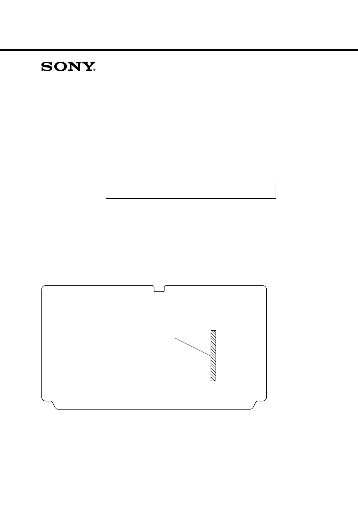
US Model
Canadian Model
1. NEW/FORMER DESCRIPTION
– DECK Board (Component Side) –
Former : 1-868-914-11
New : 1-868-914-12
9-887-123-81
Page 2

HCD-GX470/GX570
2. DIAGRAMS
• Note for Printed Wiring Boards and Schematic Diagrams
Note on Printed Wiring Board:
• X : parts extracted from the component side.
• Y : parts extracted from the conductor side.
• : Pattern from the side which enables seeing.
(The other layers' patterns are not indicated.)
• Indication of transistor
C
Q
B
E
These are omitted.
Note on Schematic Diagram:
• All capacitors are in µF unless otherwise noted. (p: pF)
50 WV or less are not indicated except for electrolytics
and tantalums.
• All resistors are in Ω and 1/
specified.
Note: The components identified by mark 0 or dotted line
with mark 0 are critical for safety.
Replace only with part number specified.
• A : B+ Line.
• Voltages and waveforms are dc with respect to ground
under no-signal (detuned) conditions.
〈〈 〉〉 : TAPE PLAY
{ }: REC
• Voltages are tak en with a V OM (Input impedance 10 MΩ).
Voltage variations may be noted due to nor mal production tolerances.
• Signal path.
E : T APE PLAY (DECK-A)
d : T APE PLAY (DECK-B)
G : REC
4
W or less unless otherwise
2
Page 3

HCD-GX470/GX570
2-1. PRINTED WIRING BOARD – DECK Section –
1 2 3 4 5 6 7
A
DECK BOARD
R481
R483
B
R482
R485
R490
C
E
R484
R489
Q405
R325
JR301
R319
E
Q406
C329
Q408
R488
E
R326
R323
C327
C330
C328
C353
JW317
JW304
JW303
R318
R349
FB301
D301
C351
R324
C324
IC301
D
R313
R311
C325
C301
R301
C317
C323
R317
C315
R309
Q301
1
4
JR302
GDS
G
C305
D
S
JW309
Q302
C302
R305
1
C326
8
C316
5
C318
CN301
R302
JR311
JW308
R310
JR303
3
E
HP1
(PB HEAD)
(DECK-A)
: Uses unleaded solder.
(Refer to page 34
on service manual)
MAIN
BOARD
D
CN201
CN008
JW302
C350
R350
R351
JW307
JW305
JW314
C352
R320
R312
R314
C304
R304
Q303
GDS
C306
C354
81
R306
R303
C303
JR310
Q304
R315
JW310
JW319
R441
R316
EE
Q409
R451
C402
C307
JW306
C430
G
R308
D
S
CN302
HRPE1
REC/PB/ERASE
HEAD
(DECK-B)
Q305
R307
R447
R439
Q306
E
Q410
R442
JW301
Q400
G
E
R402
D
R440
S
C410
R424
C355
R416
C416
R434
Q407
R443
C462
JW320
R410
R408
C356
JW311
JR404
C460
C461
JW312
C404
R414
R436
JW313
R406
C406
JW315
Q402
R412
G
S
R432
GDS
R466
JR307
C418
R446
Q401
R465
R404
C412
C414
E
D
JW316
Q404
R462
R463
R464
5
8
IC401
R428
C415
R430
R435
C433
R461
R433
C401
4
1
C431
C405
R411
C417
C411
E
Q403
R401
C456
R403
R427
JR306
R431
R445
R460
R409
C413
C403
R429
R423
A
A
R459
R405
R407
R413
C409
K
D401
C452
L451
BIAS OSC
6
4
R415
R455
R450
R456
• Semiconductor
Location
Ref. No. Location
D301 B-3
D401 C-6
IC301 C-2
IC401 C-5
Q301 D-2
Q302 D-2
Q303 D-3
Q304 D-3
Q305 D-3
Q306 D-3
Q400 C-4
Q401 D-5
Q402 D-5
Q403 D-5
R452
R454
E
Q451
R449
C458
C454
Q453
JW318
1
3
C453
Q452
R453
R458
E
R457
1-868-914-
E
JR402
12
(12)
Q404 D-5
Q405 B-1
Q406 B-1
Q407 D-4
Q408 B-2
Q409 B-3
Q410 B-4
Q451 C-7
Q452 B-7
Q453 D-7
HCD-GX470/GX570
33
Page 4

HCD-GX470/GX570
2-2. SCHEMATIC DIAGRAM – DECK Section –
(Refer to page 36
on service manual)
CN008
Q405,406,408
DECK-A/B SELECT SWITCH,
REC/PB SELECT SWITCH
R349
100
R481
4.7k
11P
REC/PB SW
REC-MUTE
DECK-D-GND
O-BIAS
A-GND
REC-R
REC-L
PB-L
PB-R
+9V
NC
FB301
0
R482
47k
C401
0.1
50V
C430
0.1
C402
0.1
50V
Q409,410
REC CONTROL SWITCH
R442
47k
R484
22k
R483
22k
Q405
C403
47p
Q409
RT1N431C
2SC3052
R485
100
R325
100 0.047
R326 C330
R403R401
22k47k
R405
47k
R406C404
47k47p
R404R402
22k47k
R455
RT1N431C
R451
2.2k
10k
2SA1235
10
Q410
R489
22k
Q406
R488
22k
R490
4.7k
0.047
C329
C433
83
2
1
IC401(1/2)
BA4558
REC AMP
IC401(2/2)
BA4558
6
7
5
4
R350
0
R323
4.7k
16V
220p
0.1
Q408
2SA1235
R351
1k
C413
220p
C414
220p
Q451,452
UDZW-TE17-4.3B
D301
R409
R411
100k
470k
R423
C417
47k
0.01
C409
10
50V
C410
10
50V
C418
R424
0.01
47k
R410
100k
Q452
2SC3052
JR402
0
0.01
C411
10p
C405
220p
R407
4.7k
R415
2.2k
R416
2.2k
R408
4.7k
C406
220p
C412
10p
REC BIAS SWITCH
R452
47k
220
C327
R319
C353
C350
22k
C352
0.1
220p
R320
22k
C351
C328
220
R324
10V
4.7k
R427
0
R445R413
0220k
C431
R440
10k
0.1
R414R412
220k470k
R446
R428
0
0
R454R453
4.7k4.7k
Q451
KTA1271Y-AT
R317
470k
C323 C325
0.0047 0.0022
C324 C326
0.0047 0.0022
R318
470k
Q403
2SA1235
REC SWITCH
R429
10k
R430
10k
Q404
2SA1235
REC SWITCH
R449 R450 R456
Q453
2SC2001
BIAS
OSC
R458
1
IC301(1/2)
NJM14558M-TE2
PB AMP
IC301(2/2)
NJM14558M-TE2
7
4
22 22 22
4.7
8
0.0022
R431
1k
D401
MC2838
R432
1k
C458
C315
R309
47p
C316
R435
0.0047
0.0047
R436
C453
0.001
R457
470
R306
220k
R313
47
R311
220
C318
10
50V
R314
47
R310
470
47p
10k
Q401
C415
2SK2158
MUTING
S
C460
C416
2SK2158
MUTING
10k
22k
470p
S
Q402
R466
0
R464
1k
R462
2.2k
1
2
34
C452
47
16V
3
2
C317
10
50V
R312
220
6
5
R433
47k
R434
47k
C454
0.0047
Q301
2SJ460
PB SWITCH
(DECK-A)
R305
220k
C462
470p
6
S
R301
47k
C305
220k
Q302
2SJ460
Q303
2SJ460
C306
220k
R465R463
01k
C456
0.01
R443
10k
S
R302
47k
R303
47k
R304
47k
Q400,407
MUTING CONTROL
SWITCH
1000p
1000p
C303
C304
C356
R441
0
PB SWITCH
(DECK-A)
S
S
PB SWITCH
(DECK-B)
S
Q304
2SJ460
PB SWITCH
(DECK-B)
Q407
2SA1235
R447
5
L451
BIAS
OSC
R439
4.7k
1M
Q400
2SK2158
R461
2.2k
R459 R460
00
C301
1000p
C302
1000p
R315
100
R316
100
C354
0.1
10
50V
JR310
0
C307
0.01
C461
470p
R307
4.7k
C355
0.01
R308
4.7k
Q305
2SC3052
MUTING
Q306
2SC3052
MUTING
CN301
CN302
3P
8P
HP1
(PB)
(DECK-A)
HRPE1
(REC/PB/ERASE)
(DECK-B)
L-CH
R-CH
ERASE
R-CH
L-CH
HCD-GX470/GX570
44
Page 5

HCD-GX470/GX570
3. ELECTRICAL PARTS LIST
NOTE:
• Due to standardization, replacements in the
parts list may be different from the parts
specified in the diagrams or the components
used on the set.
• -XX and -X mean standardized parts, so they
may have some difference from the original
one.
• RESISTORS
All resistors are in ohms.
METAL: Metal-film resistor.
METAL OXIDE: Metal oxide-film resistor.
F: nonflammable
Ref. No. Part No. Description Remark Ref. No. Part No. Description Remark
A-1171-482-A DECK BOARD, COMPLETE
*********************
< CAPACITOR/RESISTOR >
C301 1-162-964-11 CERAMIC CHIP 0.001uF 10% 50V
C302 1-162-964-11 CERAMIC CHIP 0.001uF 10% 50V
C303 1-162-964-11 CERAMIC CHIP 0.001uF 10% 50V
C304 1-162-964-11 CERAMIC CHIP 0.001uF 10% 50V
C305 1-216-849-11 METAL CHIP 220K 5% 1/10W
C306 1-216-849-11 METAL CHIP 220K 5% 1/10W
C307 1-162-970-11 CERAMIC CHIP 0.01uF 10% 25V
C315 1-162-923-11 CERAMIC CHIP 47PF 5% 50V
C316 1-162-923-11 CERAMIC CHIP 47PF 5% 50V
C317 1-126-964-11 ELECT 10uF 20% 50V
• Items marked “*” are not stocked since they
are seldom required for routine service.
Some delay should be anticipated when
ordering these items.
• SEMICONDUCTORS
In each case, u: µ, for example:
uA... : µA... uPA... : µPA...
uPB... : µPB... uPC... : µPC...
uPD... : µPD...
• CAPACITORS
uF: µF
• COILS
uH: µH
C417 1-107-726-91 CERAMIC CHIP 0.01uF 10% 16V
C418 1-107-726-91 CERAMIC CHIP 0.01uF 10% 16V
C430 1-164-156-11 CERAMIC CHIP 0.1uF 25V
C431 1-164-156-11 CERAMIC CHIP 0.1uF 25V
C433 1-162-970-11 CERAMIC CHIP 0.01uF 10% 25V
C452 1-126-947-11 ELECT 47uF 20% 35V
C453 1-130-471-00 MYLAR 0.001uF 5% 50V
C454 1-130-479-00 MYLAR 0.0047uF 5% 50V
C456 1-130-483-00 MYLAR 0.01uF 5% 50V
C458 1-130-475-00 MYLAR 0.0022uF 5% 50V
C460 1-162-962-11 CERAMIC CHIP 470PF 10% 50V
C461 1-162-962-11 CERAMIC CHIP 470PF 10% 50V
C462 1-162-962-11 CERAMIC CHIP 470PF 10% 50V
When indicating parts by reference
number, please include the board.
DECK
C318 1-126-964-11 ELECT 10uF 20% 50V
C323 1-162-968-11 CERAMIC CHIP 0.0047uF 10% 50V
C324 1-162-968-11 CERAMIC CHIP 0.0047uF 10% 50V
C325 1-162-966-11 CERAMIC CHIP 0.0022uF 10% 50V
C326 1-162-966-11 CERAMIC CHIP 0.0022uF 10% 50V
C327 1-162-960-11 CERAMIC CHIP 220PF 10% 50V
C328 1-162-960-11 CERAMIC CHIP 220PF 10% 50V
C329 1-136-161-00 MYLAR 0.047uF 5% 50V
C330 1-136-161-00 MYLAR 0.047uF 5% 50V
C350 1-126-934-11 ELECT 220uF 20% 16V
C351 1-126-934-11 ELECT 220uF 20% 16V
C352 1-107-826-11 CERAMIC CHIP 0.1uF 10% 16V
C353 1-107-826-11 CERAMIC CHIP 0.1uF 10% 16V
C354 1-107-826-11 CERAMIC CHIP 0.1uF 10% 16V
C355 1-162-970-11 CERAMIC CHIP 0.01uF 10% 25V
C356 1-126-964-11 ELECT 10uF 20% 50V
C401 1-126-956-11 ELECT 0.1uF 20% 50V
C402 1-126-956-11 ELECT 0.1uF 20% 50V
C403 1-162-923-11 CERAMIC CHIP 47PF 5% 50V
C404 1-162-923-11 CERAMIC CHIP 47PF 5% 50V
C405 1-162-960-11 CERAMIC CHIP 220PF 10% 50V
C406 1-162-960-11 CERAMIC CHIP 220PF 10% 50V
C409 1-126-964-11 ELECT 10uF 20% 50V
C410 1-126-964-11 ELECT 10uF 20% 50V
C411 1-162-915-11 CERAMIC CHIP 10PF 0.5PF 50V
C412 1-162-915-11 CERAMIC CHIP 10PF 0.5PF 50V
C413 1-162-960-11 CERAMIC CHIP 220PF 10% 50V
C414 1-162-960-11 CERAMIC CHIP 220PF 10% 50V
C415 1-162-968-11 CERAMIC CHIP 0.0047uF 10% 50V
C416 1-162-968-11 CERAMIC CHIP 0.0047uF 10% 50V
< CONNECTOR >
CN008 1-568-830-11 CONNECTOR, FFC 11P
CN301 1-815-444-11 PIN, CONNECTOR (PWB) 3P
CN302 1-815-449-11 PIN, CONNECTOR (PWB) 8P
< DIODE >
D301 6-501-165-01 DIODE UDZW-TE17-4.3B
D401 6-500-335-01 DIODE MC2838-T112-1
< JUMPER RESISTOR >
FB301 1-216-864-11 SHORT CHIP 0
< IC >
IC301 6-702-457-01 IC NJM14558M-TE2
IC401 8-759-909-71 IC BA4558F
< JUMPER RESISTOR >
JR301 1-216-864-11 SHORT CHIP 0
JR302 1-216-864-11 SHORT CHIP 0
JR306 1-216-864-11 SHORT CHIP 0
JR307 1-216-864-11 SHORT CHIP 0
JR310 1-216-864-11 SHORT CHIP 0
JR311 1-216-864-11 SHORT CHIP 0
JR402 1-216-864-11 SHORT CHIP 0
JR404 1-216-864-11 SHORT CHIP 0
< TRANSFORMER >
L451 1-443-760-11 TRANSFORMER, BIAS OSCILLATION
5
Page 6

HCD-GX470/GX570
DECK
Ref. No. Part No. Description Remark Ref. No. Part No. Description Remark
R407 1-216-829-11 METAL CHIP 4.7K 5% 1/10W
< TRANSISTOR >
R408 1-216-829-11 METAL CHIP 4.7K 5% 1/10W
Q301 6-550-290-01 FET 2SJ460-T
Q302 6-550-290-01 FET 2SJ460-T
Q303 6-550-290-01 FET 2SJ460-T
Q304 6-550-290-01 FET 2SJ460-T
Q305 8-729-120-28 TRANSISTOR 2SC1623-L5L6
Q306 8-729-120-28 TRANSISTOR 2SC1623-L5L6
Q400 8-729-045-62 FET 2SK2158-T2B
Q401 8-729-045-62 FET 2SK2158-T2B
Q402 8-729-045-62 FET 2SK2158-T2B
Q403 8-729-600-22 TRANSISTOR 2SA1235-F
Q404 8-729-600-22 TRANSISTOR 2SA1235-F
Q405 8-729-120-28 TRANSISTOR 2SC1623-L5L6
Q406 8-729-600-22 TRANSISTOR 2SA1235-F
Q407 8-729-600-22 TRANSISTOR 2SA1235-F
Q408 8-729-600-22 TRANSISTOR 2SA1235-F
Q409 6-551-276-01 TRANSISTOR RT1N431C-TP-1
Q410 6-551-276-01 TRANSISTOR RT1N431C-TP-1
Q451 8-729-037-13 TRANSISTOR KTA1271Y
Q452 8-729-120-28 TRANSISTOR 2SC1623-L5L6
Q453 8-729-011-92 TRANSISTOR 2SC2001TP-K1K2
< RESISTOR >
R301 1-216-841-11 METAL CHIP 47K 5% 1/10W
R302 1-216-841-11 METAL CHIP 47K 5% 1/10W
R303 1-216-841-11 METAL CHIP 47K 5% 1/10W
R304 1-216-841-11 METAL CHIP 47K 5% 1/10W
R305 1-216-849-11 METAL CHIP 220K 5% 1/10W
R306 1-216-849-11 METAL CHIP 220K 5% 1/10W
R307 1-216-829-11 METAL CHIP 4.7K 5% 1/10W
R308 1-216-829-11 METAL CHIP 4.7K 5% 1/10W
R309 1-216-817-11 METAL CHIP 470 5% 1/10W
R310 1-216-817-11 METAL CHIP 470 5% 1/10W
R311 1-216-813-11 METAL CHIP 220 5% 1/10W
R312 1-216-813-11 METAL CHIP 220 5% 1/10W
R313 1-216-805-11 METAL CHIP 47 5% 1/10W
R314 1-216-805-11 METAL CHIP 47 5% 1/10W
R315 1-216-809-11 METAL CHIP 100 5% 1/10W
R316 1-216-809-11 METAL CHIP 100 5% 1/10W
R317 1-216-853-11 METAL CHIP 470K 5% 1/10W
R318 1-216-853-11 METAL CHIP 470K 5% 1/10W
R319 1-216-837-11 METAL CHIP 22K 5% 1/10W
R320 1-216-837-11 METAL CHIP 22K 5% 1/10W
R323 1-216-829-11 METAL CHIP 4.7K 5% 1/10W
R324 1-216-829-11 METAL CHIP 4.7K 5% 1/10W
R325 1-216-809-11 METAL CHIP 100 5% 1/10W
R326 1-216-809-11 METAL CHIP 100 5% 1/10W
R349 1-216-809-11 METAL CHIP 100 5% 1/10W
R350 1-216-864-11 SHORT CHIP 0
R351 1-216-821-11 METAL CHIP 1K 5% 1/10W
R401 1-216-841-11 METAL CHIP 47K 5% 1/10W
R402 1-216-841-11 METAL CHIP 47K 5% 1/10W
R403 1-216-837-11 METAL CHIP 22K 5% 1/10W
R404 1-216-837-11 METAL CHIP 22K 5% 1/10W
R405 1-216-841-11 METAL CHIP 47K 5% 1/10W
R406 1-216-841-11 METAL CHIP 47K 5% 1/10W
R409 1-216-845-11 METAL CHIP 100K 5% 1/10W
R410 1-216-845-11 METAL CHIP 100K 5% 1/10W
R411 1-216-853-11 METAL CHIP 470K 5% 1/10W
R412 1-216-853-11 METAL CHIP 470K 5% 1/10W
R413 1-216-849-11 METAL CHIP 220K 5% 1/10W
R414 1-216-849-11 METAL CHIP 220K 5% 1/10W
R415 1-216-825-11 METAL CHIP 2.2K 5% 1/10W
R416 1-216-825-11 METAL CHIP 2.2K 5% 1/10W
R423 1-216-841-11 METAL CHIP 47K 5% 1/10W
R424 1-216-841-11 METAL CHIP 47K 5% 1/10W
R427 1-216-864-11 SHORT CHIP 0
R428 1-216-864-11 SHORT CHIP 0
R429 1-216-833-11 METAL CHIP 10K 5% 1/10W
R430 1-216-833-11 METAL CHIP 10K 5% 1/10W
R431 1-216-821-11 METAL CHIP 1K 5% 1/10W
R432 1-216-821-11 METAL CHIP 1K 5% 1/10W
R433 1-216-841-11 METAL CHIP 47K 5% 1/10W
R434 1-216-841-11 METAL CHIP 47K 5% 1/10W
R435 1-216-833-11 METAL CHIP 10K 5% 1/10W
R436 1-216-833-11 METAL CHIP 10K 5% 1/10W
R439 1-216-829-11 METAL CHIP 4.7K 5% 1/10W
R440 1-216-833-11 METAL CHIP 10K 5% 1/10W
R441 1-216-864-11 SHORT CHIP 0
R442 1-216-841-11 METAL CHIP 47K 5% 1/10W
R443 1-216-833-11 METAL CHIP 10K 5% 1/10W
R445 1-216-864-11 SHORT CHIP 0
R446 1-216-864-11 SHORT CHIP 0
R447 1-216-857-11 METAL CHIP 1M 5% 1/10W
R449 1-216-801-11 METAL CHIP 22 5% 1/10W
R450 1-216-801-11 METAL CHIP 22 5% 1/10W
R451 1-216-833-11 METAL CHIP 10K 5% 1/10W
R452 1-216-841-11 METAL CHIP 47K 5% 1/10W
R453 1-216-829-11 METAL CHIP 4.7K 5% 1/10W
R454 1-216-829-11 METAL CHIP 4.7K 5% 1/10W
R455 1-216-797-11 METAL CHIP 10 5% 1/10W
R456 1-216-801-11 METAL CHIP 22 5% 1/10W
R457 1-216-837-11 METAL CHIP 22K 5% 1/10W
R458 1-216-793-11 METAL CHIP 4.7 5% 1/10W
R459 1-216-864-11 SHORT CHIP 0
R460 1-216-864-11 SHORT CHIP 0
R461 1-216-825-11 METAL CHIP 2.2K 5% 1/10W
R462 1-216-825-11 METAL CHIP 2.2K 5% 1/10W
R463 1-216-821-11 METAL CHIP 1K 5% 1/10W
R464 1-216-821-11 METAL CHIP 1K 5% 1/10W
R465 1-216-864-11 SHORT CHIP 0
R466 1-216-864-11 SHORT CHIP 0
R481 1-216-829-11 METAL CHIP 4.7K 5% 1/10W
R482 1-216-841-11 METAL CHIP 47K 5% 1/10W
R483 1-216-837-11 METAL CHIP 22K 5% 1/10W
R484 1-216-837-11 METAL CHIP 22K 5% 1/10W
R485 1-216-825-11 METAL CHIP 2.2K 5% 1/10W
R488 1-216-837-11 METAL CHIP 22K 5% 1/10W
R489 1-216-837-11 METAL CHIP 22K 5% 1/10W
R490 1-216-829-11 METAL CHIP 4.7K 5% 1/10W
6
 Loading...