

Page 1
HCD-GX450
SERVICE MANUAL
Ver. 1.2 2005.08
• HCD-GX450 is the tuner, deck, CD and
amplifier section in MHC-GX450.
CD
Section
Tape deck Model Name Using Similar Mechanism New New
Section T ape Transport Mechanism T ype CWM43FF-05 CWM43FF-05
Model Name Using Similar Mechanism New New
CD Mechanism Type CDM74-F1BD81
Optical Pick-up Name
US Model
Canadian Model
Former Type Models
KSM-215DCP/C2NP KSM-213DCP/C2NP
New Type Models
CDM74KF-K6BD81C
Amplifier section
AUDIO POWER SPECIFICATIONS
POWER OUTPUT AND TOTAL HARMONIC
DISTORTION:
With 6 ohm loads, both channels driven, from
120 – 10,000 Hz: rat ed 125 watts per ch annel
minimum RMS power, with no more than 10%
total harmonic distortion from 250 milliwatts to
rated output.
Front speaker
Continuous RMS power output (reference):
125 + 125 watts (6 ohms at
1 kHz, 10% THD)
Total harmonic distortion less than 0.07% (6 ohms at
1kHz, 60 W)
Sub woofer
Continuous RMS power output (reference):
150 watts (6 ohms at
50 Hz, 10% THD)
Total harmonic distortion less than 0.07% (6 ohms at
50 Hz, 75 W)
CD player section
System Compact disc and dig ital
audio system
SPECIFICATIONS
Laser Semiconductor laser
(λ=780 nm)
Emission duration:
continuous
Frequency response 2 Hz – 20 kHz (± 0.5 dB)
Wavelength 780 – 790 nm
Signal-to-noise ratio More than 90 dB
Dynamic range More than 90 dB
Tape deck section
Recording system 4-track 2-channel, stereo
Frequency response 50 – 13,000 Hz (±3 dB),
using Sony TYPE I
cassettes
Tuner section
FM stereo, FM/AM super he te rodyne tuner
FM tuner section
Tuning range 87.5 – 108.0 MHz
(100-kHz step)
Antenna FM lead antenna
Antenna terminals 75 ohms unbalanced
Intermediate frequency 10.7 MHz
AM tuner section
Tuning range 530 – 1,710 kHz
(with the tuning interv al
set at 10 kHz)
531 – 1,710 kHz
(with the tuning interv al
set at 9 kHz)
Antenna AM loop antenna
Antenna terminals External antenna terminal
Intermediate frequency 450 kHz
General
Power requirements 120 V AC, 60 Hz
Power consumption
USA models: 265 watts
Canadian models: 330 VA
Dimensions (w/h/d) incl. projecting parts and controls
Amplifier/Tuner/Tape/CD section:
Approx. 280 × 327 ×
425 mm
Mass Approx. 10.0 kg
Design and specifications are subject to change
without notice.
9-877-534-03
2005H16-1
© 2005.08
MINI HI-FI COMPONENT SYSTEM
Sony Corporation
Personal Audio Group
Published by Sony Engineering Corporation
Page 2
HCD-GX450
SAFETY CHECK-OUT
After correcting the original service problem, perform the
following safety checks before releasing the set to the customer:
Check the antenna terminals, metal trim, “metallized” knobs, screws,
and all other exposed metal parts for AC leakage. Check leakage as
described below.
LEAKAGE
The AC leakage from any exposed metal part to earth ground
and from all exposed metal parts to any exposed metal part having
a return to chassis, must not exceed 0.5 mA (500 microamperes).
Leakage current can be measured by any one of three methods.
1. A commercial leakage tester, such as the Simpson 229 or RCA
WT -540A. Follo w the manufacturers’ instructions to use these
instruments.
2. A battery-operated AC milliammeter. The Data Precision 245
digital multimeter is suitable for this job.
3. Measuring the voltage drop across a resistor by means of a
VOM or battery-operated AC v oltmeter. The “limit” indication
is 0.75 V, so analog meters must have an accurate low-voltage
scale. The Simpson 250 and Sanwa SH-63Trd are e xamples of
a passive VOM that is suitable. Nearly all battery operated
digital multimeters that have a 2V AC range are suitable. (See
Fig. A)
To Exposed Metal
Parts on Set
AC
0.15 µF
1.5 kΩ
Earth Ground
Voltmeter
(0.75 V)
The release method of a CD disc tray LOCK function
There is a disc lock function for the disc theft prevention for a
demonstration at a shop front in this machine.
Procedue:
1. Press the ?/1 button to turn the set on.
2. Press two buttons of x and Z (EJECT) simultaneously for
five seconds.
3. The message “LOCKED” is displayed and the tray is locked.
(Even if exiting from this mode, the tray is still locked.)
4. Press two buttons of x and Z (EJECT) simultaneously for
five seconds again.
5. The message “UNLOCKED” is displayed and the tray is
unlocked.
6. To exit from this mode, press the ?/1 button to turn the set
off.
Unleaded solder
Boards requiring use of unleaded solder are printed with the leadfree mark (LF) indicating the solder contains no lead.
(Caution: Some printed circuit boards may not come printed with
the lead free mark due to their particular size.)
: LEAD FREE MARK
Unleaded solder has the following characteristics.
• Unleaded solder melts at a temperature about 40°C higher than
ordinary solder.
Ordinary soldering irons can be used but the iron tip has to be
applied to the solder joint for a slightly longer time.
Soldering irons using a temperature regulator should be set to
about 350°C.
Caution: The printed pattern (copper foil) may peel away if the
heated tip is applied for too long, so be careful!
• Strong viscosity
Unleaded solder is more viscous (sticky , less prone to flow) than
ordinary solder so use caution not to let solder bridges occur such
as on IC pins, etc.
• Usable with ordinary solder
It is best to use only unleaded solder but unleaded solder may
also be added to ordinary solder.
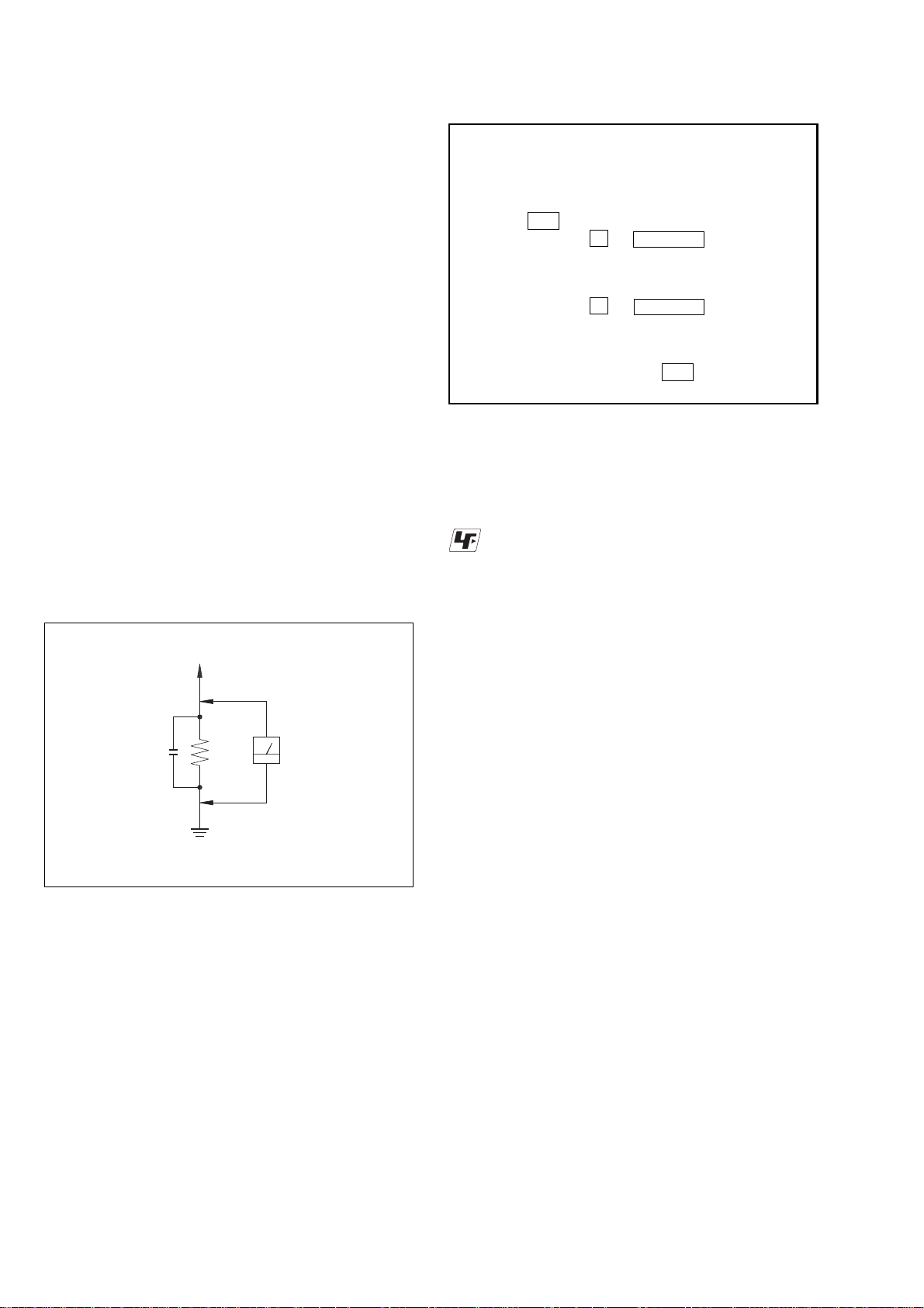
Fig. A. Using an A C v oltmeter to check A C leakage.
SAFETY-RELATED COMPONENT WARNING!!
COMPONENTS IDENTIFIED BY MARK 0 OR DOTTED LINE WITH
MARK 0 ON THE SCHEMATIC DIAGRAMS AND IN THE PARTS
LIST ARE CRITICAL TO SAFE OPERATION. REPLACE THESE
COMPONENTS WITH SONY PARTS WHOSE PART NUMBERS
APPEAR AS SHOWN IN THIS MANUAL OR IN SUPPLEMENTS
PUBLISHED BY SONY .
ATTENTION AU COMPOSANT AYANT RAPPORT
LES COMPOSANTS IDENTIFÉS P AR UNE MARQUE 0 SUR LES
DIAGRAMMES SCHÉMA TIQUES ET LA LISTE DES PIÈCES SONT
CRITIQUES POUR LA SÉCURITÉ DE FONCTIONNEMENT. NE
REMPLACER CES COMPOSANTS QUE PAR DES PIÈSES SONY
DONT LES NUMÉROS SONT DONNÉS DANS CE MANUEL OU
DANS LES SUPPÉMENTS PUBLIÉS PAR SONY.
À LA SÉCURITÉ!
2
Page 3
HCD-GX450
NOTES ON HANDLING THE OPTICAL PICK-UP
BLOCK OR BASE UNIT
The laser diode in the optical pick-up block may suffer electrostatic
break-down because of the potential difference generated by the
charged electrostatic load, etc. on clothing and the human body.
During repair, pay attention to electrostatic break-down and also
use the procedure in the printed matter which is included in the
repair parts.
The flexible board is easily damaged and should be handled with
care.
NOTES ON LASER DIODE EMISSION CHECK
The laser beam on this model is concentrated so as to be focused on
the disc reflective surface by the objective lens in the optical pickup block. Therefore, when checking the laser diode emission,
observe from more than 30 cm away from the objective lens.
Laser component in this product is capable
of emitting radiation exceeding the limit for
Class 1.
TABLE OF CONTENTS
1. SERVICING NOTE·························································· 4
2. GENERAL ·········································································· 6
3. DISASSEMBLY
3-1. Cover (Top) ····································································· 9
3-2. CD Door·········································································· 9
3-3. Front Panel Section ······················································· 10
3-4. CD Mechanism Deck (CDM74-F1BD81) ···················· 10
3-5. Tape Mechanism Deck, Game Jack Board ··················· 11
3-6. PANEL Board ······························································· 11
3-7. Back Panel Section, SUB-TRANS Board ···················· 12
3-8. Power Transformer······················································· 12
3-9. MAIN Board ································································· 13
3-10. SUB-WOOFER Board················································ 13
3-11. AMP Board ································································· 14
3-12. BD81A Board ····························································· 14
3-13. CONNECT Board·······················································15
3-14. DRIVER Board, SW Board ········································ 15
3-15. Optical Pick-up (KSM-215DCP/C2NP) ····················· 16
3-16. SENSOR Board ·························································· 16
3-17. MOTOR (TB) Board··················································· 17
3-18. MOTOR (LD) Board ·················································· 17
4. TEST MODE ···································································· 18
This appliance is classified as a CLASS 1 LASER product. The
CLASS 1 LASER PRODUCT MARKING is located on the rear
exterior.
CAUTION
Use of controls or adjustments or performance of procedures
other than those specified herein may result in hazardous radiation
exposure.
Notes on chip component replacement
•Never reuse a disconnected chip component.
• Notice that the minus side of a tantalum capacitor may be
damaged by heat.
Flexible Circuit Board Repairing
•Keep the temperature of soldering iron around 270˚C
during repairing.
• Do not touch the soldering iron on the same conductor of the
circuit board (within 3 times).
• Be careful not to apply force on the conductor when soldering
or unsoldering.
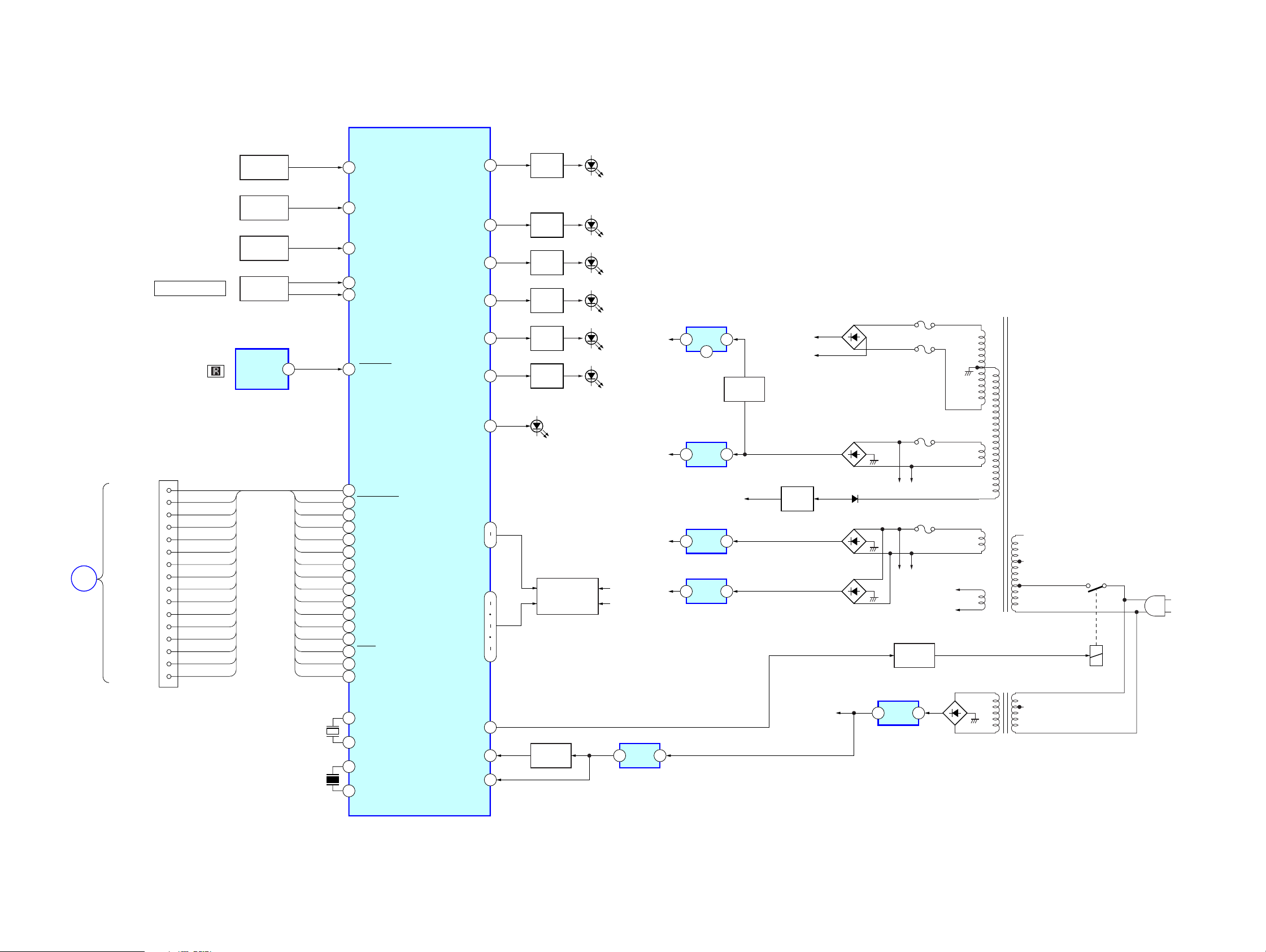
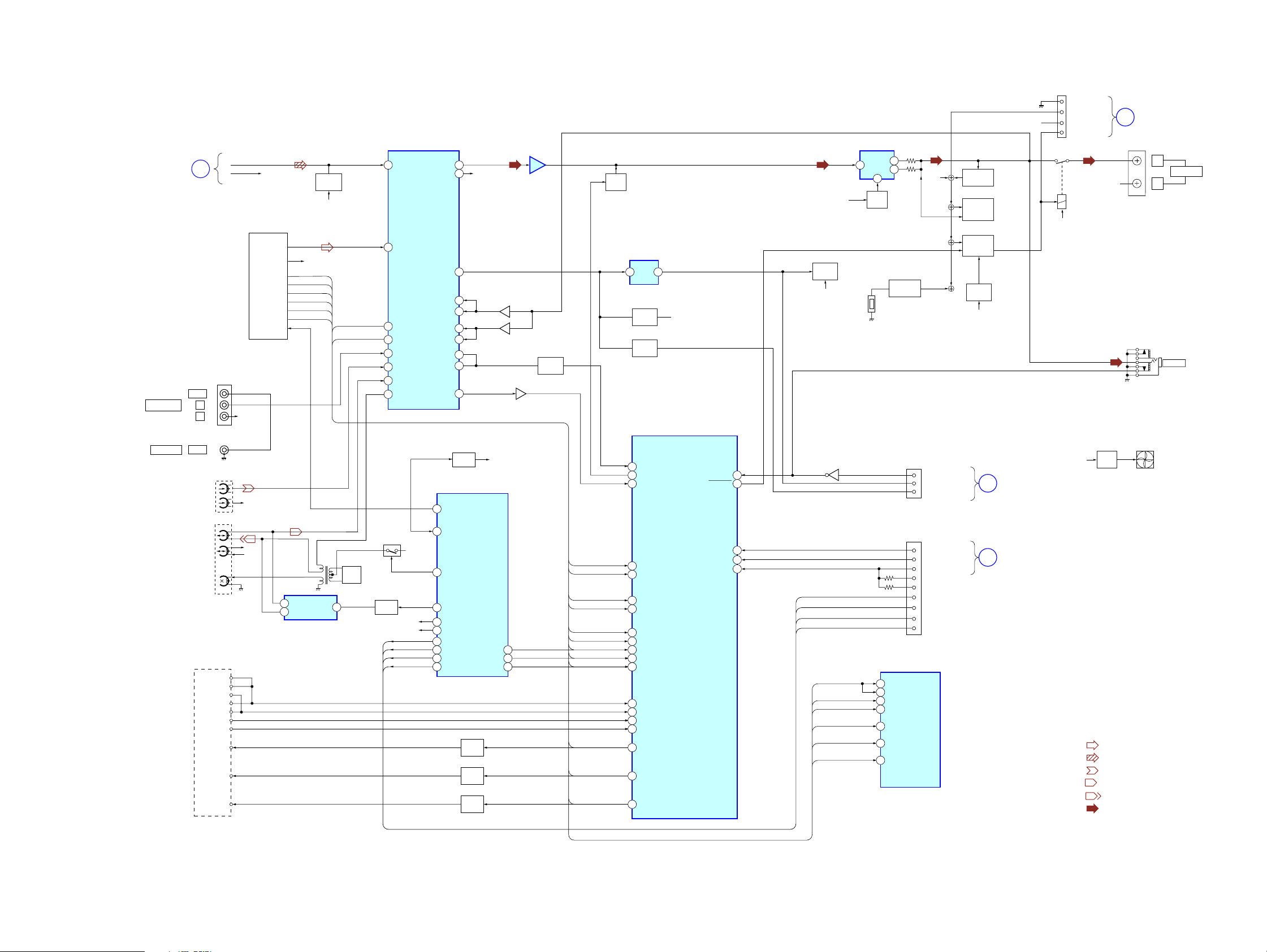
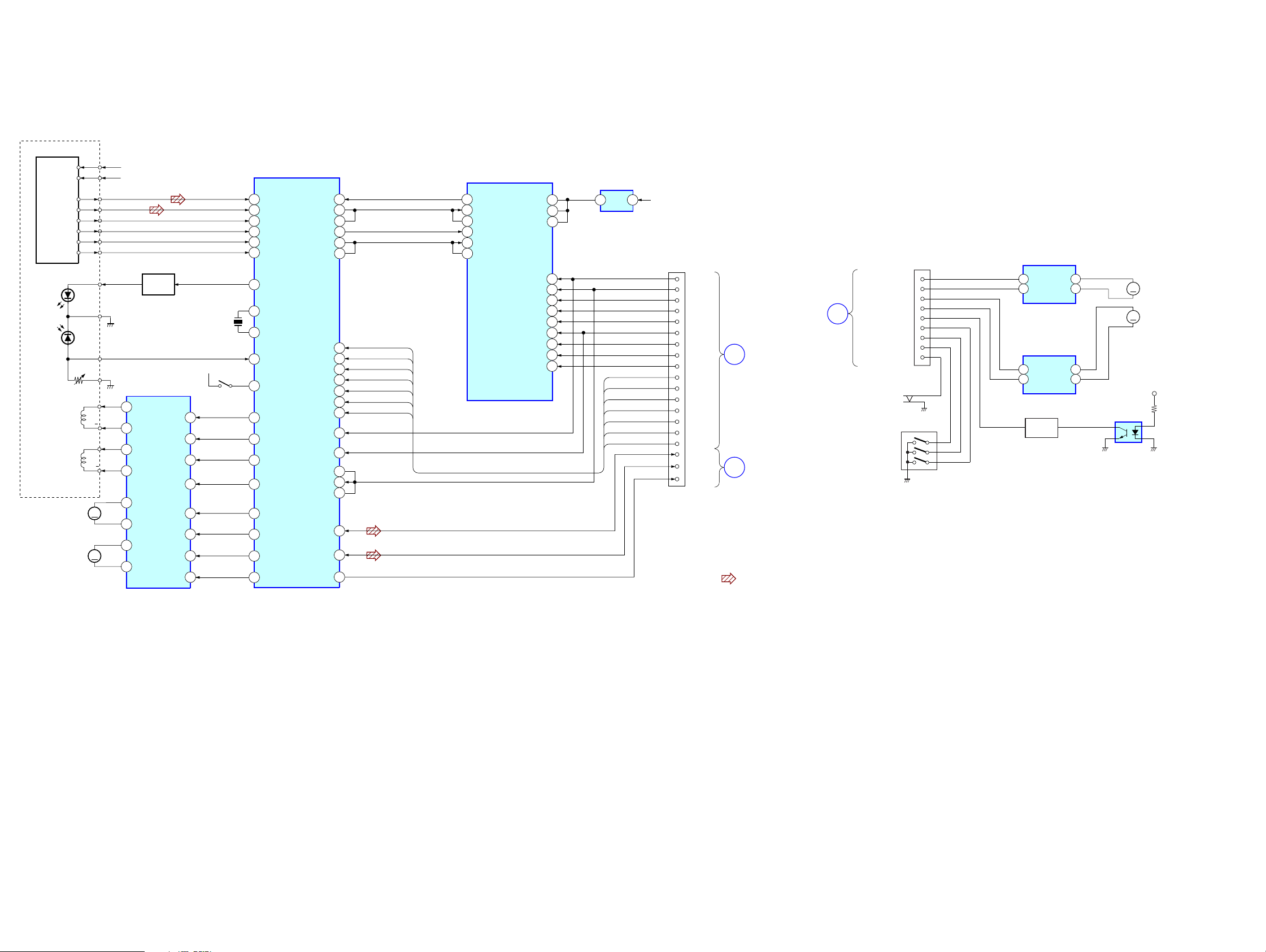
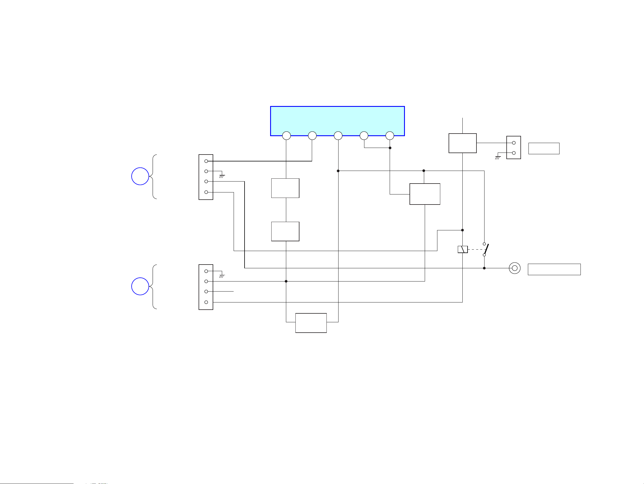
5. DIAGRAMS
5-1. Block Diagrams – PANEL Section – ···························· 22
– MAIN Section – ······················································· 23
– BD/DRIVER Section – ············································ 24
– SUB-WOOFER Section – ········································ 25
5-2. Printed Wiring Board – BD81A Section –··················· 26
5-3. Schematic Diagram – BD81A Section – ····················· 27
5-4. Printed Wiring Board
– CD MECHANISM Section – ··································· 28
5-5. Schematic Diagram – CD MECHANISM Section –···29
5-6. Printed Wiring Board – MAIN Section – ···················· 30
5-7. Schematic Diagram – MAIN Section (1/2) – ·············· 31
5-8. Schematic Diagram – MAIN Section (2/2) – ·············· 32
5-9. Printed Wiring Board – PANEL COMB Section – ······ 33
5-10. Schematic Diagram – PANEL COMB Section – ······ 34
5-11. Printed Wiring Board – SUB-WOOFER Section – ··· 35
5-12. Schematic Diagram
– SUB-WOOFER Section – ········································ 36
5-13. Printed Wiring Board – PANEL Section –················· 37
5-14. Schematic Diagram – PANEL Section (1/2) – ·········· 38
5-15. Schematic Diagram – PANEL Section (2/2) – ·········· 39
5-16. Printed Wiring Board – TRANS Section – ················ 40
5-17. Printed Wiring Board – AMP Section – ····················· 41
5-18. Schematic Diagram – AMP POWER Section – ········ 42
5-19. IC Pin Function Description ······································· 46
6. EXPLODED VIEWS
6-1. MAIN Section·······························································51
6-2. Front Panel Section ······················································· 52
6-3. MAIN Board Section ···················································· 53
6-4. CD Mechanism Deck Section -1 (CDM74-F1BD81)··· 54
6-5. CD Mechanism Deck Section -2 (CDM74-F1BD81)··· 55
7. ELECTRICAL PARTS LIST ······································· 56
3
Page 4
HCD-GX450
d
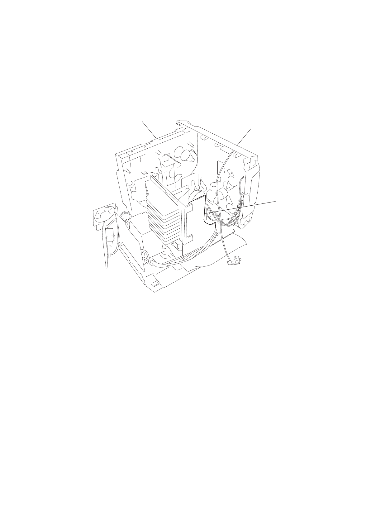
• SERVICE POSITION -1 (AMP BOARD)
To inspect the AMP board, turn both of the front panel
and the CD mechanism deck so that the left side of the product faces down.
CD mechanism deck
SECTION 1
SERVICING NOTE
front panel
AMP boar
4
Page 5
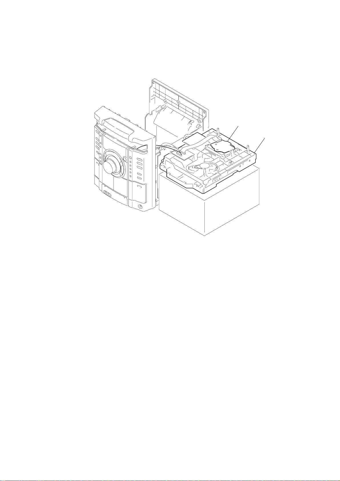
• SERVICE POSITION -2 (BD81A BOARD)
k
Remove the CD mechanism deck and place it on top of the pedestal as shown.
Inspect the BD81A bard in this set up.
HCD-GX450
BD81A board
CD mechanism dec
5
Page 6
HCD-GX450
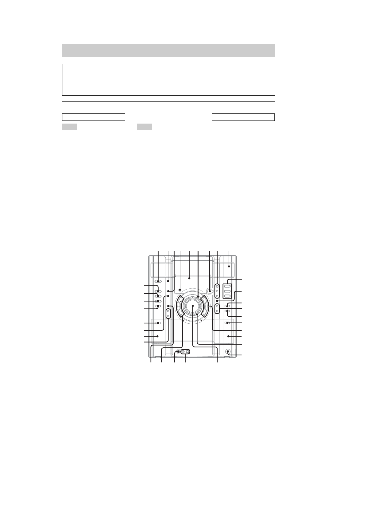
Illustrati
SECTION 2
GENERAL
List of button locations and reference pages
How to use this page
Use this page to find the loca tio n of buttons and other
parts of the system that are mentioned in the text.
Main unit
ALPHABETICAL ORDER
A – O P – Z
ALBUM +
ALBUM –
CD eg (9, 11, 14, 19, 20)
CD SYNC wj (19)
Deck A wk (18)
Deck B qj (18, 19, 20, 24)
DISC 1 – 3 q; (12, 14, 35)
DISC SKIP/EX-CHANGE qs
Disc tray 9 (11)
DISPLAY 2 (17, 27, 28)
Display window 5
EFFECT ON/OFF 8 (22)
ENTER qa (14, 15 , 22)
EQ BAND 7 (22)
GAME es (20, 23, 30)
GAME INPUT AUDIO L/R jacks
GAME INPUT VIDEO jack wf
GAME MIXING wh (23)
GROOVE 8 (21)
ILLUMINATION
Operation Dial
qh (12, 14, 19)
wg (12, 14, 19)
(11, 12, 14, 19)
wd (20, 29)
(29)
3 (28)
(– EQ +/l L) 6 (12,
14, 19, 22)
P FILE qd (22)
PHONES jack ql
PLAY MODE wl (12, 14, 18, 19,
20, 35)
Power illuminator qk (28)
PRESET EQ qd (22)
REC PAUSE/START wj (19, 20,
23, 24)
Remote sensor 4
SURROUND 8 (23)
TAPE A/B ed (18, 19, 20, 24)
TUNER/BAND ef (15, 16, 20)
TUNING MODE wl (15, 16, 35)
TUNING + qh (15, 16)
TUNING – wg (15, 16)
VOLUME control w; (21)
12345 6 78 9
eg
ef
ed
es
e;
wl
wk
wj
on number
r
TAPE A/B ed (18, 19, 20, 24)
Name of button/pa rt Reference page
RR
BUTTON DESCRIPTIONS
?/1 (power) 1 (8, 16, 27, 30, 33,
35)
X (pause) wg (12, 19)
Z (eject) qf (11)
PUSH Z (deck B) (eject) qg (18)
x (stop) wg (12, 19, 24, 35)
M (fast forward) qh (12, 19)
H (play) qh (12, 18, 19)
m (rewind) wg (12, 19)
Z PUSH (deck A) (eject) e; (18)
q;
qa
j
ALBUM
S
s
TUNING TUNING
J
ALBUM
H
h
qs
qd
qf
qg
qh
qj
qk
ql
6
wh
wfwg
wd
w;
Page 7
HCD-GX450
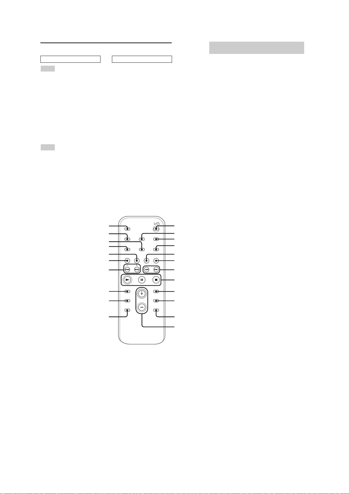
Remote control
ALPHABETICAL ORDER
A – E
ALBUM – qd (12, 14)
ALBUM + qa (12, 14)
CD qk (11, 14)
CLEAR qg (14)
CLOCK/TIMER SELECT 2
(26, 27)
CLOCK/TIMER SET 3 (10, 25,
26)
DISC SKIP q; (12, 14)
DISPLAY wa (17, 27, 28)
ENTER 9 (10, 14, 15, 25, 26)
EQ qf (22)
F – Z
FM MODE 4 (17)
FUNCTION 6 (11, 14, 15, 16)
PLAY MODE w; (12, 14, 18)
REPEAT 4 (13)
SLEEP ws (25)
TAPE qj
TUNER BAND 5 (15, 16)
TUNER MEMORY ql (15)
TUNING MODE w; (15, 16)
VOLUME +/– qs (21, 25)
BUTTON DESCRIPTIONS
?/1 (power) 1 (8, 26)
m/M (rewind/fast forward)
7 (12, 19)
–/+ (tuning) qh (15)
./> (go back/go forward)
qh (10, 12, 19)
N (play) 8 (12, 18)
X (pause) 8 (12, 19)
x (stop) 8 (12, 19)
Setting the clock
Use buttons on the remote for the operation.
1
Press ?/1 to turn on the system.
2
Press CLOCK/TIMER SET.
3
Press . or > repeatedly to set the
hour.
4
Press ENTER.
5
Press . or > repeatedly to set the
minute.
6
Press ENTER.
The clock starts working.
To adjust the clock
1
Press CLOCK/TIMER SE T.
2
Press . or > repeatedly to select
“CLOCK SET”, then press ENTER.
3
Do the same procedures as step 3 to 6
above.
Notes
The clock settings are canceled when you disconnect
the power cord or if a power failure occurs.
ws
wa
w;
ql
qk
qj
qh
qg
qf
qd
1
2
3
4
5
6
7
8
9
q;
qa
qs
7
Page 8
HCD-GX450
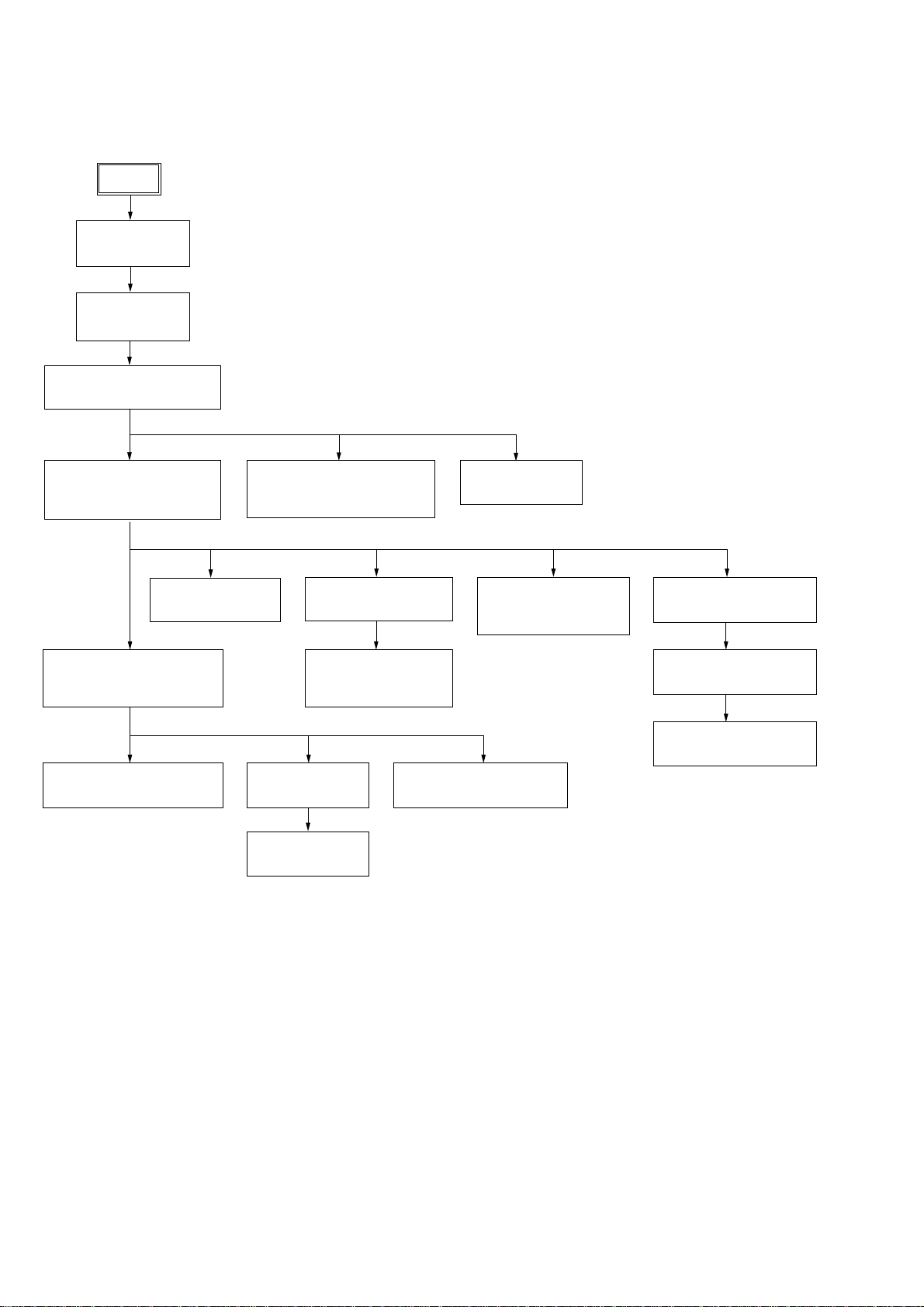
Note: Disassemble the unit in the order as shown below.
SET
3-1.COVER (TOP)
(Page 9)
3-2.CD DOOR
(Page 9)
SECTION 3
DISASSEMBLY
3-3.FRONT PANEL SECTION
(Page 10)
3-4.CD MECHANISM DECK
(CDM74-F1BD81)
(Page 10)
3-12.BD81A BOARD
(Page 14)
3-7.BACK PANEL SECTION,
SUB-TRANS BOARD
(Page 12)
3-8.POWER TRANSFORMER
(Page 12)
3-5.TAPE MECHANISM DECK,
GAME JACK BOARD
(Page 11)
3-13.CONNECT BOARD
(Page 15)
3-14.DRIVER BOARD,
SW BOARD
(Page 15)
3-9.MAIN BOARD
(Page 13)
3-10.SUB-WOOFER BOARD
3-6.PANEL BOARD
(Page 11)
3-15.OPTICAL PICK-UP
(KSM-215DCP/C2NP)
(Page 16)
(Page 13)
3-16.SENSOR BOARD
(Page 16)
3-17.MOTOR (TB) BOARD
(Page 17)
3-18.MOTOR (LD) BOARD
(Page 17)
3-11.AMP BOARD
(Page 14)
8
Page 9
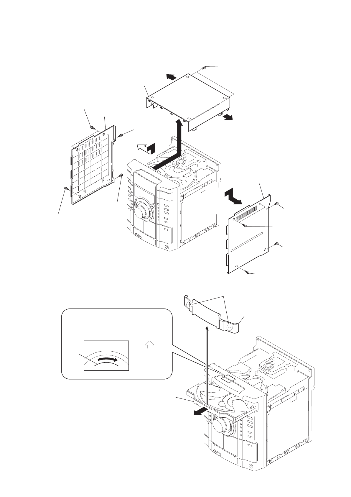
Note: Follow the disassembly procedure in the numerical order given.
3-1. COVER (TOP)
qs
qf
cover
(top)
6
two screws (Case 3 TP2)
cover
(Side-L)
qa
two
screws (+BVTP 3
×
HCD-GX450
10)
7
screw (case 3 TP2)
3-2. CD DOOR
9
screw
(+BVTP 3
× 10
)
8
screw
(+BVTP 3
q;
× 10
qs
)
qd
cover
(Side-R)
5
3
3
two claws
(+BVTP 3
1
two screws
(case 3 TP2)
4
(+BVTP 3
2
screw (Case 3 TP2)
screw
screw
× 10
× 10
)
)
CD mechanism deck (CDM74)
1
Turn the pulley to the direction of arrow.
Front panel side
pulley
2
Pull-out the disc tray.
4
CD door
9
Page 10
HCD-GX450
)
3-3. FRONT PANEL SECTION
0
connector 3p (CN304C)
8
wire (flat type) 17 core (CN253)
6
connector 2p (CN805)
3
screw (+BVTP 3
×
10)
4
screw (+BVTP 3
× 8
)
5
screw (+BVTP 3
× 8
)
qd
front panel section
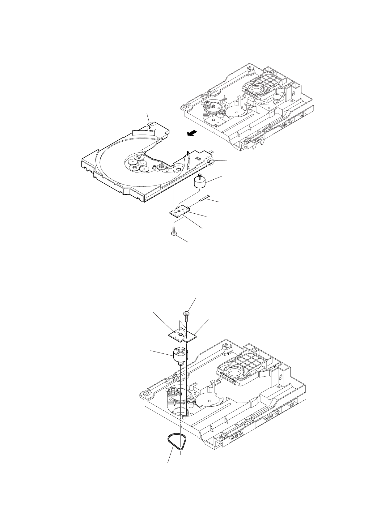
3-4. CD MECHANISM DECK (CDM74-F1BD81)
2
screw (+BVTP 3
qs
connector 8p (CN103)
9
connector 5p (CN309)
7
wire (flat type) 29 core (CN302)
1
three screws (+BVTP 3
qa
connector 3p (CN102B)
× 8
)
1
three
×
10)
screws (+BVTP 3
×
10
10
4
CD mechanism deck (CDM74-F1BD81)
3
connector 9p (CN254)
2
connector 12p (CN701)
Page 11
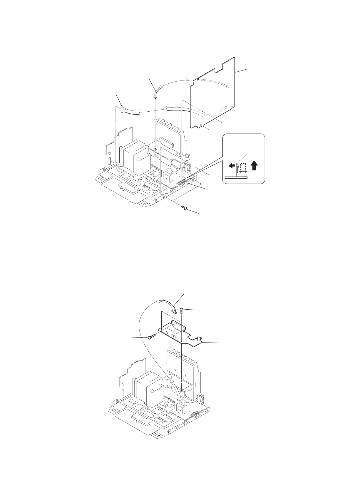
3-5. TAPE MECHANISM DECK, GAME JACK BOARD
)
)
1
wire (flat type) 13 core (CN602)
3
tape mechanism deck
HCD-GX450
2
six
screws
(+BVTP 2.6
×
8
3-6. PANEL BOARD
2
seven
claws
5
GAME JACK board
4
two
(+BVTP 2.6
3
connector 6p (CN604)
screws
×
8)
4
connector 5p (CN605)
5
PANEL board
1
ten
screws
×
(+BVTP 2.6
8
11
Page 12
HCD-GX450
)
r
3-7. BACK PANEL SECTION, SUB-TRANS BOARD
7
8
SUB-TRANS board
6
(+BVTT 3
1
connector
2p (CN904)
two
screws
× 10
)
connector
2p (CN901)
3
connector
3p (CN308)
9
back panel section
5
(+BVTT 3
three
screws
×
10)
4
two
screws
(+BVTP 3
×
10
3-8. POWER TRANSFORMER
1
connector
3p (CN905)
2
wire (flat type) 11 core (CN101)
5
four
screws
(+ITC 4
× 8
)
6
power transforme
3
screw
(+BVIT 3
× 8R
)
12
2
connector
10p (CN907)
4
earth wire
Page 13
3-9. MAIN BOARD
d
d
1
connector
10p (CN907)
2
connector
4p (CN501)
5
MAIN
Main board
HCD-GX450
boar
3-10. SUB-WOOFER BOARD
2
two
(transistor)
screws
4
13p (CN441)
3
two
(+BVTP 3
1
connector
7p (CN502)
3
two
(+BVTP 3
connector
screws
× 8
)
screws
× 8
)
4
SUB-WOOFER boar
13
Page 14
HCD-GX450
)
)
3-11. AMP BOARD
3
two
screws
(+BVIT 3
4
two
screws
(transistor)
× 8R
)
6
AMP
2
screw
(+BVTP 3
board
×
14)
1
two
screws
(+BVTP 3
5
heat sink
× 8
3-12. BD81A BOARD
4
Remove soldering from the four points.
1
wire (flat type) 27 core (CN202)
3
screw
(+BVTP 2.6
5
BD81A
board
× 8
)
2
wire (flat type) 16 core (CN101
14
Page 15
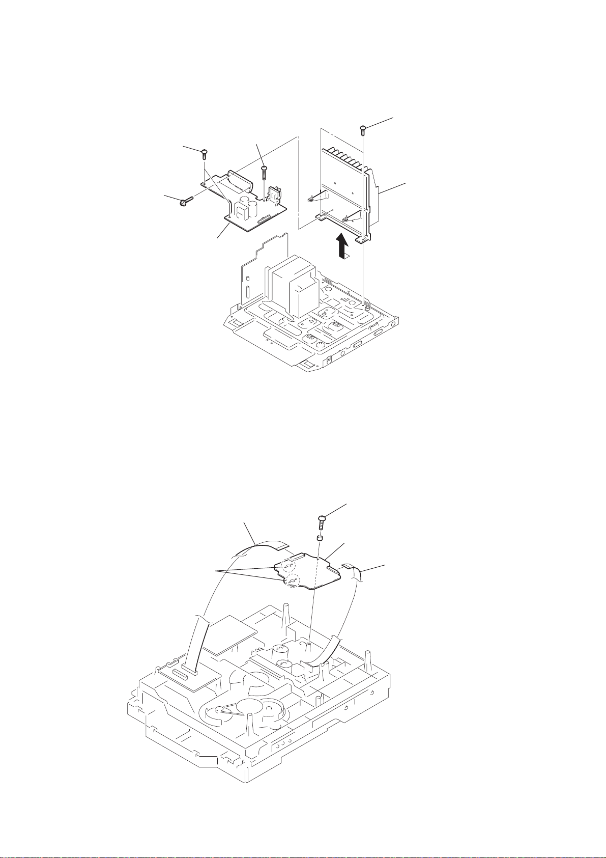
3-13. CONNECT BOARD
2
two
(+BVTP 2.6
3
CONNECT
screws
board
1
wire (flat type) 27 core (CN251)
× 8
)
HCD-GX450
3-14. DRIVER BOARD, SW BOARD
1
(+BTTP (M2.6))
4
DRIVER
2
wire (flat type) 5p (CN702)
two
screws
board
3
connector
4p (CN703)
5
screw
(+BTTP (M2.6))
6
SW board
15
Page 16
HCD-GX450
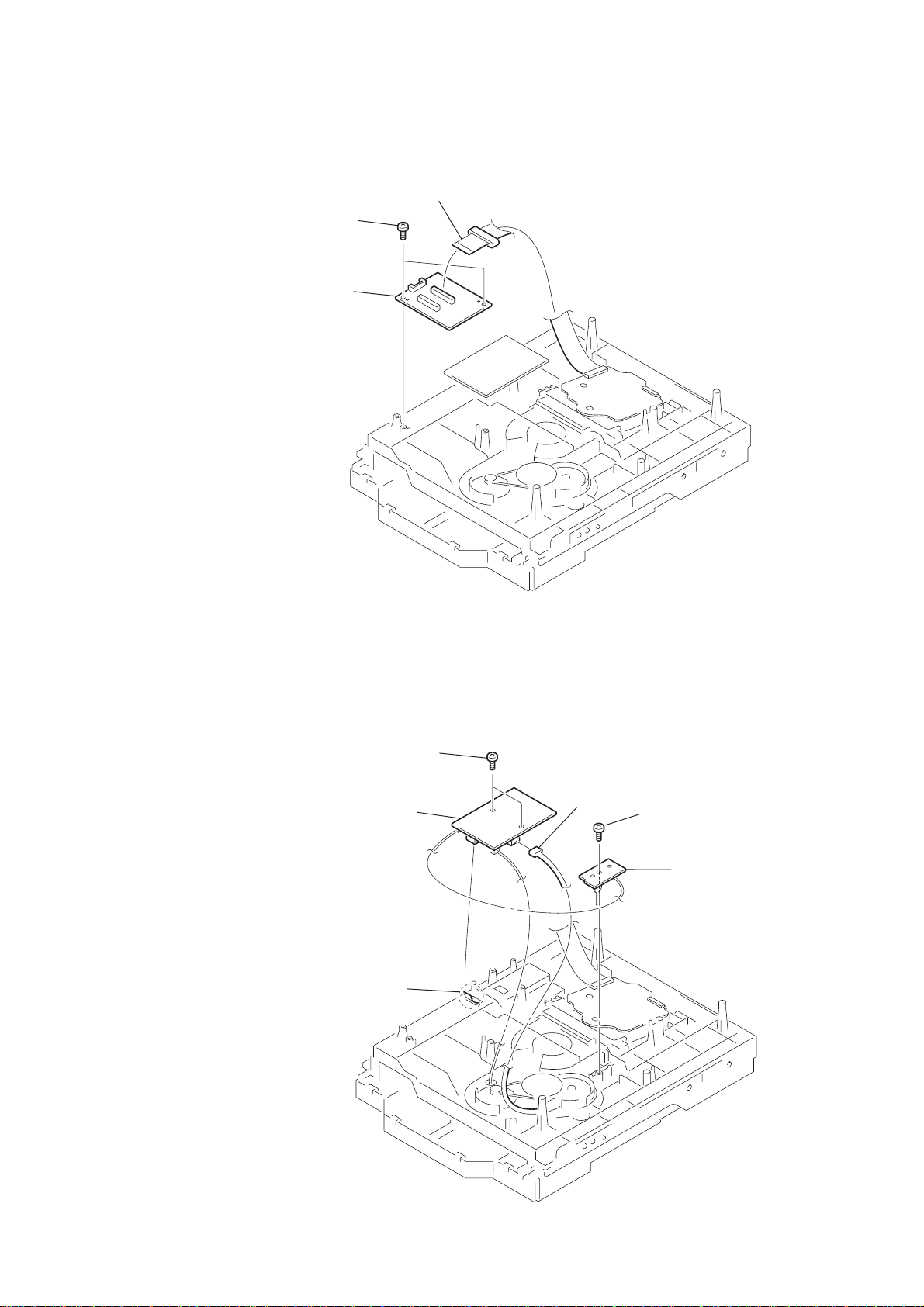
3-15. OPTICAL PICK-UP (KSM-215DCP/C2NP)
2
h
qh
optical pick-up
(KSM-215DCP/C2NP)
0
two
insulators
9
two
coil springs
(insulator)
8
t
wo stoppers (BU)
older (213) ASSY
qa
1
floating
(+PTPWH M2.6)
6
two
insulators
5
two
coil springs
(insulator)
3
screw
(BVTT M2.6)
4
floating
(+PTPWH M2.6)
screw
screw
3-16. SENSOR BOARD
2
t
ray
7
(BVTT M2.6)
qd
Remove the four solderings of motor.
1
floating
(+PTPWH M2.6)
6
floating
(+PTPWH M2.6)
screw
8
s
(+BTTP (M2.6))
screw
t
wo screws
crew
0
SENSOR board
9
connector
(
CN731)
qf
CN101 (flat type)
qg
B
D81A board
qs
s
crew (+BVTP 2.6x 8)
3
b
elt (table)
4
floating
(+PTPWH M2.6)
5
screw
p
ulley (table)
16
7
g
ear (geneva)
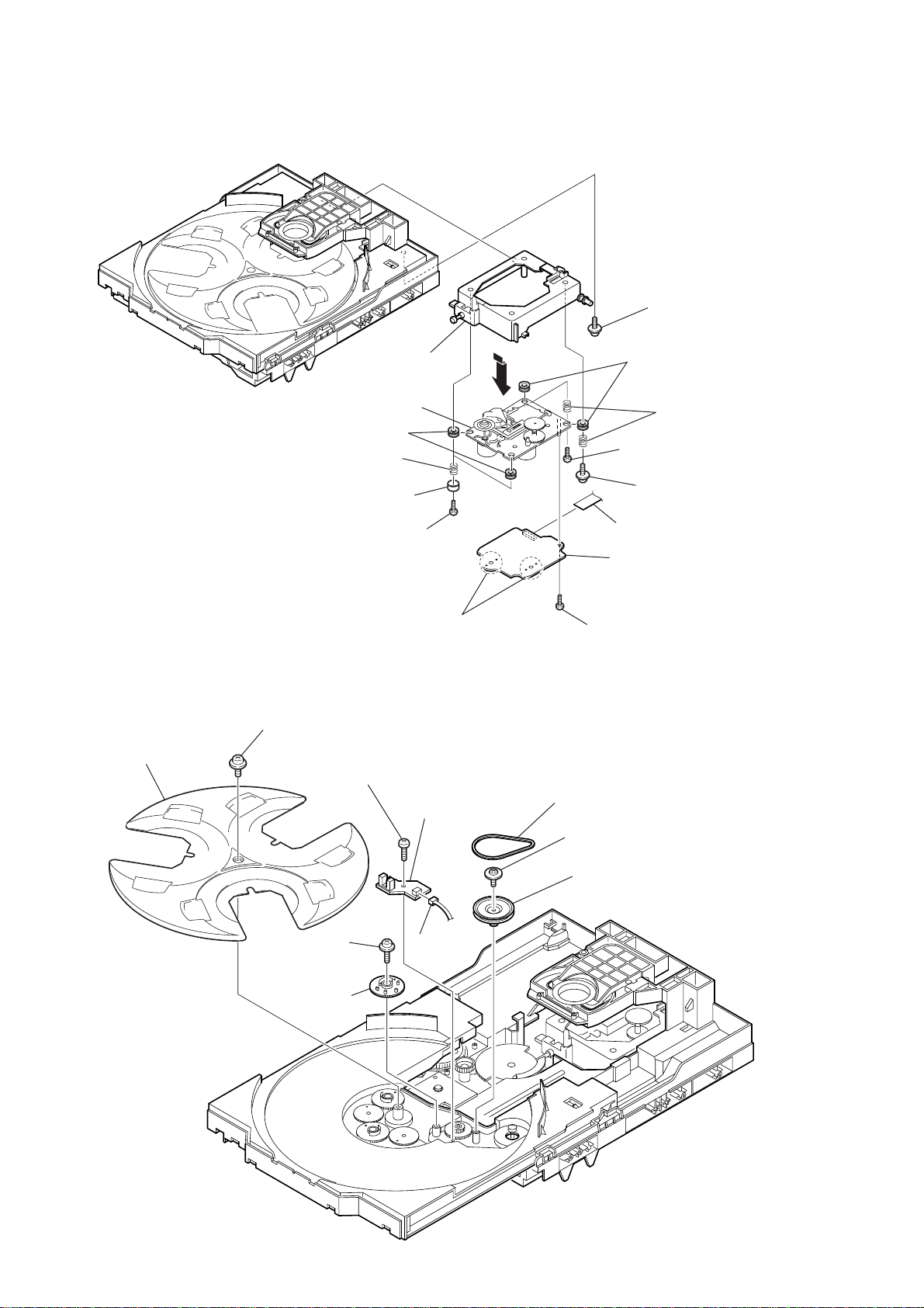
Page 17
3-17. MOTOR (TB) BOARD
2
stopper
4
1
stopper
5
t
able motor assy (M741)
HCD-GX450
3-18. MOTOR (LD) BOARD
4
Remove the two solderings of motor.
5
l
oading motor assy (M751)
3
7
MOTOR (TB) board
6
Remove the two solderings of motor.
5
two
screws
(+BTTP (M2.6))
2
two
screws
(+BTTP (M2.6))
3
MOTOR (LD) board
wire (flat type) 5 core (CN742)
1
b
elt (loading)
17
Page 18
HCD-GX450
SECTION 4
TEST MODE
[Change-over of AM Tuner Step between 9 kHz and
10 kHz]
•A step of AM channels can be changed ov er between 9 kHz and
10 kHz.
Procedure:
1. Press ?/1 button to turn the set ON.
2. Select the function “TUNER”, and press TUNER/BAND
button to select the BAND “AM”.
3. Press ?/1 button to turn the set OFF.
4. Press PLAY MODE/TUNING MODE and ?/1 buttons si-
multaneously, and the display of fluorescent indicator tube
changes to “AM 9 k STEP” or “AM 10 k STEP”, and thus the
channel step is changed over.
[Cold Reset]
• The cold reset clears all data including preset data stored in the
RAM to initial conditions. Execute this mode when returning
the set to the customer.
Procedure:
1. Press three buttons x , PLAY MODE/TUNING MODE ,
and DISC 1 simultaneously.
2. The fluorescent indicator tube displays “COLD RESET” and
the set is reset.
[Aging Mode]
This mode can be used for operation check of CD section and tape
deck section.
• If an error occurred:
The aging operation stops and is displayed status.
• If no error occurs:
The aging operation continues repeatedly.
1. Operating method of Aging Mode
Press ?/1 button to turn the set ON and select “CD” of the function.
1) Set three discs in tray. Press the
PLA Y MODE/TUNING MODE
button to set the “ALL DISCS” mode, and the PRESET EQ
button to “REPEAT” off.
2) Load the tapes recording use into both decks.
3) Press three buttons x , PLAY MODE/TUNING MODE ,
and EX-CHANGE simultaneously.
4) Aging operations of CD and tape are started at the same time.
5) To exit the aging mode, perform [Cold Reset].
2. Aging mode in CD section
1) Operation during aging mode
• In the agining mode ,the program is excuted in the following
sequence.
(1) The disc tray opens and closes.
(2) The disc tray turns to select a disc 3.
(3) The pick-up accesses to the first track, and plays 3 seconds.
(4) The pick-up accesses to the last track, and plays 3 seconds.
(5) The disc tray opens and closes.
(6) The disc tray turns to select a disc 1.
(7) The same operation starts like step (3).
(8) After a disc 1 aging operation, a disc 2 is selected.
(9) When an aging operation of a disc 3 is completed, the display
“AGING ∗∗∗∗” value increases.
(10) If no error occurs, the aging operation continues repeatedly.
2) Error display
Disc error
Display Error
E00D01022 Focus error (No disc)
E00D02022 Sub Q error (Focus is good)
E00D02023 TOC reading error
E00D02014 Access error (Unable within regular time)
Mechanism error
Display Error
E00M__E_0 Error during opening tray
E00M__C_2 EX-CHANGE disc error
E00M__D_0 Error during closing tray
E00M__F_3 EX-OPEN error
E00M__D_5 EX-CLOSE error
E00M__C_2 Chuck-up error
E00M__C_3 Unchucking error
3. Aging mode in Tape Deck section
1) Operation during aging mode
• In the agining mode, the program is excuted in the following
sequence.
Step
1
Rewind the TAPE A
2
Rewind the TAPE B
3
Play the TAPE A (1 minute)
4
Stop the TAPE A (1 second)
5
Play the TAPE A (3 minutes)
6
Rewind(AMS) the TAPE A
7
F.F.(AMS) the TAPE A
8
Play the TAPE B (1 minute)
9
Stop the TAPE B (1 second)
10
Record the TAPE B (3 minutes)
11
Rewind(AMS) the TAPE B
12
F.F.(AMS) the TAPE B
Operation
Display
TAPE AAG-1
TAPE BAG-2
TAPE AAG-2
TAPE AAG-3
TAPE AAG-4
TAPE AAG-5
TAPE AAG-6
TAPE BAG-2
TAPE BAG-3
TAPE BAG-4
TAPE BAG-5
TAPE BAG-6
2) Error display
• If error occurred, the display remains like “TAPE BAG-2”.
4. Exiting from the aging mode
• Be sure to perform Cold Reset to exit from the aging mode.
18
Page 19
HCD-GX450
[P ANEL Test Mode]
• All fluorecent segments and LEDs are tested.
•Keyboard check.
Procedure:
1. Press ?/1 button to turn the set ON.
2. To enter the test mode, press the three buttons x , PLAY
MODE/TUNING MODE and ENTER simultaneously.
3. All segments and LEDs (without STANDBY LED) are turned
on.
4. Press X and ENTER buttons simultaneously, and the key
check mode is activated.
5. The message “KEY 0 0 0 ” is displayed.
Each time a button is pressed, the key code number is displayed.
6. Press X and ENTER buttons simultaneously, and the key
count mode is activated.
7. The message “KEYCNT 0” is displayed.
Each time a button is pressed, “KEYCNT 0” value increased.
However, once a button is pressed, it is no longer taken into
account.
8. Press X and ENTER buttons simultaneously, and the head
phone detect mode is activated.
9. The message “H_P OFF” is displayed when a headphone jack
is not inserted.
“H_P ON ” is displayed when a headphone jack is inserted.
10. Press X and ENTER b uttons simultaneously , and the volume
control detect mode is activated.
11. The message “VOLUME FLAT” is displayed.
“VOLUME UP” is displayed if rotating MASTER VOLUME
knob clockwise, or “VOLUME DO WN” is displayed if rotating
counterclockwise.
12. To exit from the GC test mode after the head phone detect mode,
press X and ENTER buttons simultaneously.
[Version and Destination Display Mode]
•The version or destination is displayed.
Procedure:
1. Press ?/1 button to turn the set ON.
2. To enter the test mode, press the three buttons x , PLAY
MODE/TUNING MODE and DISC 2 simultaneously.
3. The destination is displayed.
4. Press DISPLAY buttons simultaneously.
5. The version is displayed.
6. To exit from this mode, press the three buttons x , PLAY
MODE/TUNING MODE and DISC 2 simultaneously and
press ?/1 button to turn the set OFF.
[CD Service Mode]
•This mode can run the CD sled motor freely. Use this mode, for
instance, when cleaning the pick-up.
Procedure:
1. Press ?/1 button to turn the set ON.
2. Select the function “CD”.
3. To enter the test mode, press three b uttons x , PLAY MODE/
TUNING MODE , and Z simultaneously.
4. The CD service mode is selected.
5. With the CD in stop status, press M button to move the
pick-up to outside track, or press m button to inside track.
6. To exit from this mode, perform as follows:
1) Move the pick-up to the most inside track.
2) Press ?/1 button to turn the set OFF.
Note: • Always move the pick-up to most inside track when exiting from
this mode. Otherwise, a disc will not be unloaded.
• Do not run the sled motor excessively, otherwise the gear can be
chipped.
[MC Test Mode]
•This mode is used to test the function of the equalizer.
Procedure:
1. Press ?/1 button to turn the set ON.
2. To enter the test mode, press the three buttons x , PLAY
MODE/TUNING MODE and DISC 3 simultaneously.
3. Press the EQ + button.
The function of the equalizer is set to “MAX”.
4. Press the EQ - button.
The function of the equalizer is set to “MIN”.
5. Press the PRESET EQ button.
The function of the equalizer is set to “EQ FLAT”.
6. MASTER VOLUME up and down.
“VOLUME MIN” “VOLUME 16” “VOLUME MAX” is
displayed.
7. Press the GROOVE button.
The message “VACS OFF” or “VACS ON” is displayed.
8. To exit from this mode, press ?/1 button to turn the set OFF.
[CD Ship Mode (LOCK) ]
•This mode moves the pick-up to the position durable to vibra-
tion. Use this mode when returning the set to the customer after
repair.
Procedure:
1. Press ?/1 button to turn the set ON.
2. Select the function “CD”.
3. Press ?/1 button to turn the set OFF.
4. Press CD button and ?/1 button simultaneously.
5. The “ST ANDBY” display blinks instantaneously, the message
“LOCK” is displayed and the CD ship mode is set.
[CD Ship (LOCK) & COLD RESET MODE]
Procedure:
1. Press ?/1 button to turn the set ON.
2. Select the function “CD”.
3. Press ?/1 button to turn the set OFF.
4. Press three buttons x , CD and DISPLAY simultaneously.
5. The “ST ANDBY” display blinks instantaneously and CD ship
mode is set.
6. To fluorescent indicator tube displays “COLD RESET” and
the set is reset.
[Disc T ray Lock]
Procedure:
1. Press the ?/1 button to turn the set ON.
2. Select the function “CD”.
3. Press two buttons of x and Z simultaneously for f ive seconds.
4. The message “LOCKED” is displayed and the tray is locked.
(Even if exiting from this mode, the tray is still locked.)
5. Press two buttons of x and Z simultaneously for five seconds
again.
6. The message “UNLOCKED” is displayed and the tray is
unlocked.
7. To exit from this mode, press the ?/1 button to turn the set
OFF.
19
Page 20

HCD-GX450
[CD Repeat 5 Times Limit Release Mode]
Procedure:
1. Press ?/1 button to turn the set ON.
2. Select the function “CD”.
3. Press three buttons x , CD and ENTER simultaneously.
4. The message “LIMIT OFF” is displayed.
5. Press ?/1 button the set OFF.
[AMP TEST MODE]
Procedure:
1. Press ?/1 button to turn the set ON.
2. To enter the test mode, press three buttons x , PLAY
MODE/TUNING MODE and ENTER simultaneously.
3. Press the DISPLAY button.
The message “V0 0 0” “ 000” is displayed.
4. Press the GROOVE button.
The message “DBFB ON” “DBFB OFF” is displayed.
5. Press the SURROUND button.
The message “SURROUND ON” “SURROUND OFF” is
displayed.
6. Press the EQ BAND button.
The message “LOW” “MID” “HIGH” is displayed.
7. Press ?/1 button to turn the set OFF.
20
Page 21
SECTION 5
d
DIAGRAMS
THIS NOTE IS COMMON FOR PRINTED WIRING BOARDS AND SCHEMA TIC DIAGRAMS.
(In addition to this, the necessary note is printed in each bloc k.)
Note on Schematic Diagram:
• All capacitors are in µF unless otherwise noted. pF: µµF
50 WV or less are not indicated except for electrolytics
and tantalums.
• All resistors are in Ω and 1/
specified.
f
•
• C : panel designation.
• A : B+ Line.
• B : B– Line.
• H : adjustment for repair.
•Voltages and waveforms are dc with respect to ground
•Voltages are taken with a VOM (Input impedance 10 MΩ).
•Waveforms are taken with a oscilloscope.
• Circled numbers refer to waveforms.
• Signal path.
: internal component.
Note:
The components identified by mark 0 or dotted
line with mark 0 are critical for safety.
Replace only with part
number specified.
under no-signal (detuned) conditions.
Voltage variations may be noted due to normal produc-
tion tolerances.
no mark : FM
( ): CD STOP
Voltage variations may be noted due to normal production tolerances.
F : TUNER
E : PB (DECK A)
d : PB (DECK B)
G : REC (DECK B)
J : CD
f : AUDIO
4
W or less unless otherwise
Note:
Les composants identifiés par
une marque 0 sont critiques
pour la sécurité.
Ne les remplacer que par une
piéce portant le numéro
spécifié.
Note on Printed Wiring Boards:
• X : parts extracted from the component side.
• b : Pattern from the side which enables seeing.
Caution:
Pattern face side: Parts on the pattern face side seen from
(SIDE A) the pattern face are indicated.
Parts face side: Parts on the parts face side seen from
(SIDE B) the parts face are indicated.
• Indication of transistor.
C
These are omitted.
Q
B
CE
These are omitted.
•Abbreviation
CND : Canadian model
Q
B
HCD-GX450
Circuit Boards Location
SENSOR board
SW board
MOTOR (LD) board
CONNECT board
E
TRANS board
SUB-TRANS board
BD81A board
MOTOR (TB) board
DRIVER board
SUB-WOOFER boar
AMP board
VIDEO OUT board
• Waveforms
– PANEL BOARD –
1 IC601 qd (I-XT2)
30.5 s
2 V/DIV, 10 s/DIV
2 IC601 qh (CF2)
100 ns
2 V/DIV, 40 ns/DIV
5.2 Vp-p
4.9 Vp-p
REM board
PANEL board
MAIN board
6 STREAM LED board
GAME JACK board
H/P JACK board
2121
Page 22
HCD-GX450
5-1. BLOCK DIAGRAMS – PANEL SECTION –
IC601(1/2)
SYSTEM CONTROLLER
BD/DRIVER
SECTION
A
SCOR
XTCN
XRST
XL-T-CD
CD-DATA
SENS
CD-CLK
MP3-DO
MP3-DI
MP3-CLK
MP3-CS
MP3-CP
MP3-ACK
MP3-REQ
MP3-RESET
MP3-STB
MASTER VOLUME
CN603
C1
C2
C3
C4
C5
C6
C7
C8
C9
C10
C11
C12
C13
C14
C15
C18
S641-S650
FUNCTION
KEY
S601-S612
FUNCTION
KEY
S621-S630
FUNCTION
KEY
S851
ENCODER
IC610
REMOTE
CONTROL
RECIEVER
C18
C15
C14
C13
C12
C11
C10
C9
C8
C7
C6
C5
C4
C3
C2
C1
X601
32.768kHz
X602
10MHz
25 KEY3
27 KEY1
26 KEY2
9 VOLUME-IN1
10 VOLUME-IN2
283 SIRDS-IN
MP3-TTB
80
MP3-RESET
6
MP3--REQ
4
MP3-ACK
3
MP3-CS
2
MP3-CS'
1
MP3-CLK
100
MP3-DI
99
MP3-DO
98
CD-CLK
97
SENS
96
CD-DATA
95
XLT
94
XRES
93
XTCN
92
SCOR
5
12 I-XT1
13 I-XT2
15 CF1
16 CF2
G01-G13
S1-S21
POWER RELAY
Q610
82STREM-LED1
80STREM-LED3
81STREM-LED2
77STREM-LED6
78STREM-LED5
79STREM-LED6
76POWER LED
42
30
43
45
47
50
52
65
74
11RESET
29ACCUT
LED
DRIVER
Q612
LED
DRIVER
Q611
LED
DRIVER
Q614
LED
DRIVER
Q615
LED
DRIVER
Q613
LED
DRIVER
LED601
FLUORESCENT
INDICATOR
Q605
RESET
SWITCH
FL601
TUBE
LED610
LED612
LED611
LED615
LED614
LED613
VF
-VFL
IC604
RESET
+3.5V
+3.5V
+9V
+9V
PT901
POWER TRANSFORMER
VF
D902-905
SUB TRANSFORMER
RY901
AC
IN
PT902
AC3
AC4
IC603
REG
F904
F905
F906
F907
RELAY
DRIVE
15
IC302
REG
12
4
Q301,Q302
SWITCH
IC301
REG
13
-VFL
IC303
REG
13
IC304
REG
13
13
+B
-B
Q902
REG
D401
D301-D304
D902
D305-D308
D309-D312
Q361,Q362,Q314,Q315
+3.3V
2222
Page 23
– MAIN SECTION –
BD/DRIVER
SECTION
GAME INPUT
VIDEO OUT
B
J804
VIDEO
L
R
J803
VIDEO
DECK-A
LRHP2
HP1
DECK-B
L
HRP2
R
HRP1
HE1
TAPE
MECHANISM DECK
PWDEWC B
MODE B
MODE A
B HALF
A HALF
A-PHOTO
B-PHOTO
COMP
SOLA
CD-L
CD-R
R-CH
R-CH
R-CH
R-CH
TUNER
TUNER-L
TUNER-R
CLK
TUNED
STEREO
TU-MUTE
DO
DI
CE
Q304-Q307
REC SW
9
P/B SW
7
SELECTOR
IC201
CD-MUTE
R-CH
CLK
TUNED
STEREO
CONT
SWITCH
DO
DI
CE
L101
4
DATA
RCLK
Q321
BIAS
OSC
1 CDL
61 TUNER_L
19 SI
18 SO
59 GAME-L
9 TAPEA1
11 TAPEB1
15 REC-OUT1
Q324
Q322,Q323
SWITCH
IC101
SOUND PROCESSOR
+9V
CD-MUTE
FAN
LM-R
LM-F
TM-R
TM-F
BBNF1
BBIN1
BBNF2
SAOUT2
SAOUT1
11 Q5
12 Q6
7Q1
6Q0
10 Q4
17 Q11
13 Q7
14 Q8
15 Q9
16
32VOUT2
33VOUT1
25 5 1SW OUT
34
35
31BBNF2
30
55
56
40ASMOUT
Q308,Q309
Q313
SWITCH
IC371
SP DRIVER
Q601
CAP M
DRIVE
Q602
B TRIG
DRIVE
Q603
A TRIG
DRIVE
R-CH
STK
DATA
CLOCK
LCH
Q106
BUFFER
Q107
BUFFER
Q327
BUFFER
3
4
5Q10
IC102
BUFFER
Q351,Q352
SWITCH
RCLK
DATA
TUNED
STEREO
DI
CE
DO
CLK
LCH
MOTOR
SOLB
SOLA
MUTE
Q101-Q104
IC104
BUFFER
Q105
SWITCH
Q303
DEF
SYSTEM CONTORLLER
24 I-STREEMA/VACS
75 SYSTEM-MUTE
69 ASM
88
CLK
91
DATA
67
TUNED
68
STEREO
83
DI
84
CE
85
DO
CLK
86
LCH
87
23
TAPE B START+
22
TAPE A START+
I-REEL-A
70
I-REEL-B
71
2
MOTOR
3
SOLBSOLB
4
SOLA
+Vcc
IC601(2/2)
HCD-GX450
CN443
GND
OVERLOAD/DC
RY441
+B
RELAY+
RELAY-
FAN
Q310-Q312
FAN
DRIVE
+10V
IC441
POWER AMP
11
Q108
SWITCH
-VFL
TH441
Q371
19WFR/HP/MIC
18PROTECT
INVERTER
4
5
13
Q489
MUTESTK
Q483,Q484
OVERHEAT
R-CH
DET
Q481,Q482
OVERLOAD
DET
Q441,Q442
OVERLOAD
DET
Q485-Q488
RELAY
DRIVE
SWITCH
AC4
Q308,
Q309,Q313
CN306
SW ON/OFF
SW OUT
SW LIMITER
C
SUB-WOOFER
SECTION
CN201
IC602
VIDEO BUFFER
CD NO SENS
CD OPEN/CLOSE
CD ENCORDER
BD/DRIVER
D
SECTION
• R-CH is omitted due to same as L-CH
• Signal Path
73SENSOR
21CD-OPEN/CLOSE
20CD ENCORDER
LM-R
LM-F
TM-R
TM-F
DO
CLK
LCH
SOL-A
SOL-B
MOTOR
3 DATA
18 SO
4 CLK
5 LCK
6 SOL-A
7
SOL-B
8
MOTOR
E
JK441
R-CH
: TUNER
: CD
: PB(DECK A)
: PB(DECK B)
: REC(DECK B)
: AUDIO
SUB-WOOFER
SECTION
L
R
FAN
SPEAKER
J801
PHONES
2323
Page 24
HCD-GX450
– BD/DRIVER SECTION –
OPTICAL PICK-UP
BLOCK
(KSM-215DCP/C2NP)
DETECTOR
VCC
FOCUS
COIL
TRACKING
COIL
(SPINDLE)
M102
(SLED)
VC
A
B
C
D
E
F
LD
GND
PD
VR
M101
+1.7V
+3.3V
Q10
DRIVER
IC251
SL/SP MOTOR
DRIVER
F+
16
CH2OUT-F
F
15
CH2OUT-R
T+
17
CH1OUT-R
T
18
CH1OUT-F
19
CH4OUT-F
M
20
CH4OUT-R
21
CH3OUT-R
M
CH3OUT-F
22
LD
CH1FIN
CH1RIN
CH2FIN
CH2RIN
SFDR
SRDR
OPIN+
MUTE
IC301
11
SDO0
16
LRCKIA
19
SFSY/LRCK1B
14
SDIO
15
BCKIA
18
SBSY/BCK1B
DIGITAL SIGNAL
PROCESSOR
PO11/BUCK/AD1
SRMSTB
VDD
VDD
VDDM
STANBY
MIACK
MICK
MIDIO
MILP
MICS
RESET
IC303
55
21
40
3
36
8
7
6
5
4
2
41
5 1
REG
SCOR
SENS
CLOCK
XLT
DATA
XRST
XTACN
3.3V
CN201
MP3STB
MP3REQ
MIACK
MICK
MIDIO
MILP
MICS
MP3RST
SRMSTB
SCOR
SENS
CLOCK
XLT
DATA
XRST
XTACN
LOUT
ROUT
DOUT
• R-CH is omitted due to same as L-CH
• Signal Path
PANEL
SECTION
A
MAIN
SECTION
B
: CD
MAIN
SECTION
D
LMR
LMF
TM-R
TM-F
TBL ADDRESS SW
E-1
E-2
E-3
OPEN SW
(LEVER SW)
E-3
E-2
E-1
CN701
S751
RE701
ROTARY
ENCODER
IC701
(LD)MOTOR DRIVER
RIN
OUT1
9
FIN
9
7
IC712
RIN
FIN
Q731
SWITCH
OUT2
OUT1
OUT2
11
TBL MOTOR DRIVER
4
2
4
2
M
M
IC731
(TABLE SENSOR)
M751(LOADING)
M741(TBL)
+3V
IC101
RF AMP
26
A
27
B
28
C
29
D
19
E
20
F
36
LD
XTAO
100
77
78
37
11
12
13
14
30
29
7
6
XTAI
PD
SSTP
TFDR
TRDR
FFDR
FRDR
CH3FIN
CH3RIN
MPD
XRST
X171
16.9MHz
+3.3V
SW101
5
6
7
8
9
10
3
24
PCMD1
LRCK1
LRCK
PCMD
BCK
BCK1
XTACN
XRST
DATA
XLAT
CLOCK
SENS
SCOR
GFS
C2PO
FOK
AOUT1
AOUT2
DOUT
100
102
104
105
107
115
113
114
61
62
63
65
66
60
95
1
2
3
81
86
71
XTACN
XRST
DATA
XLAT
CLOCK
SENS
SCOR
2424
Page 25
– SUB-WOOFER SECTION –
HCD-GX450
IC501
AMP
+B
MAIN
SECTION
MAIN
SECTION
C
E
CN501
SW-SIG-IN
GND
SW-LIMIT
SW-SENCE
CN502
GND
OVERLOAD/DC
RELAY+ +B
PT-2
2
Q507
DETECT
Q503
DETECT
SW IN
3
-RE
8 12
+RE
13
Q502
CN503
SWITCH
CONTROL
Q501
OVERCOAR
DETECT
RY501
JK501
SUB WOOFER OUT
RELAY-
Q506,Q505
DETECT
2525
Page 26
HCD-GX450
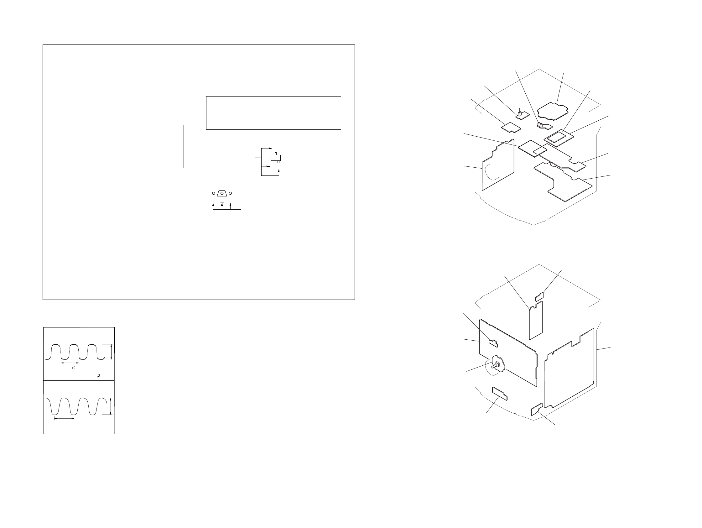
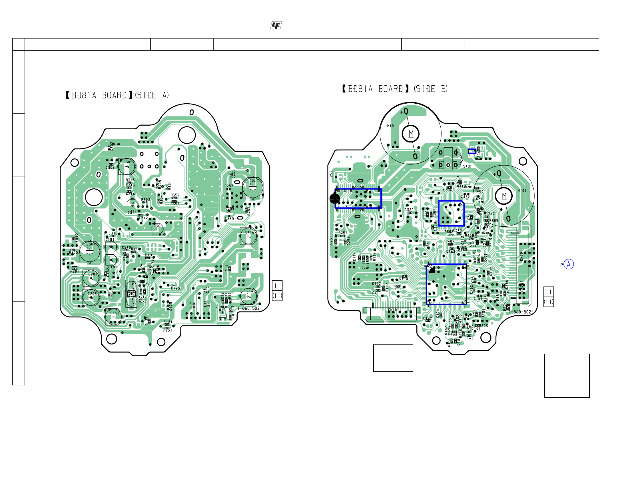
5-2. PRINTED WIRING BOARD – BD81A SECTION –
12
A
B
• See page 21 for Circuit Boards Location.
• : Uses unleaded solder .
3456789
SPINDLE
MOTOR
IC303
1
3
5
4
(LIMIT)
C
D
E
IC301
SLED
MOTOR
IC251
CONNECT
IC101
E
• Semiconductor
OPTICAL
PICK-UP
BLOCK
(KSM–215DCP)
BOARD
CN251
(Page 33)
Location
Ref. No. Location
IC101 D-7
IC251 C-6
IC301 C-7
IC303 B-7
Q10 E-4
2626
Page 27
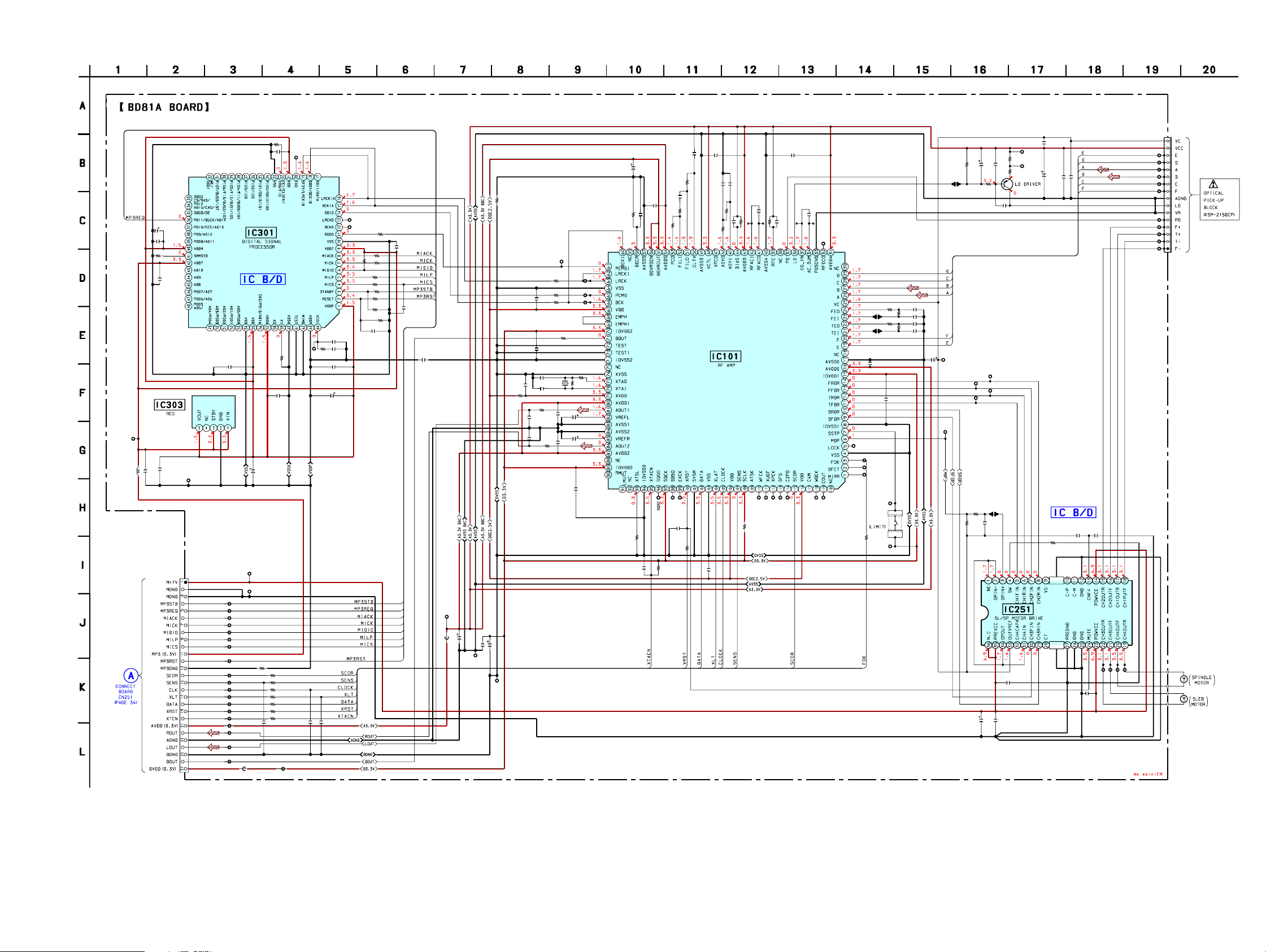
HCD-GX450
5-3. SCHEMATIC DIAGRAM – BD81A SECTION –
R307
10k
TP433
MP3VDD
FB301
BLM21B272S
0.1 F
C307
0.1 F
C308
47
4V
C309
R303
100k
C310
0.1 F
IC303
BH15FB1W
C302
C303
0.1
0.1
F
F
TP422
MP3GND
CN201
27P
C311
0.1 F
TP401
TP402
TP403
TP404
TP405
TP406
TP407
TP408
TP417
TP416
TP415
TP414
TP413
TP412
TP419
TP434
TP410
TP411
TP409
IC301
TC94A34FG-002
C305
TP186
MVDD
TP187
MGND
MP3STB
MP3REQ
MIACK
MICK
MIDIO
MILP
MICS
MP3RST
R205
SCOR
SENS
CLK
XLT
DATA
XRST
XTCN
AVDD
ROUT
LOUT
DOUT
R204
0
TP304
0.0022 B
TP
301
0
306
R
C312
0.1 F
220
4V
0
R411
R410
R409
R408
R407
R406
R412
C213
22p CH
R313
0.1 B
220
100
100
100
100
100
100
100
22p CH
C212
TP435
C211
DVDD
• See page 46 for IC PIN FUNCTION DESCRIPTION.
C10C11
C15
10
F
C13
NM
R253
10k
IC251
BA5947FM
(HSOP28)
10
6.3
6.3
B
B
C259
0.1
C258
F
0.1
+
L-
SL+
SP
S
3
5
252
251
TP
TP
TP2
F
57
C2
0.1
0.1
B
C134
0.1 F
015
C142
C151
100
10V
0
1
R203
0
TP302
TP303
R351
100
10k
R405
R404
R419
R403
R402
R401
R301
C317
0.01 B
0.1 F
47 4V
C306
0.1 F
100
100
100
100
100
100
C318
0.01
B
100k
R305
100k
C320
0
C174
0.1 F
TP436
AVDD
C201
100
0
10V
R201
TP420
AGND
C203
100
10V
B
209
C
0.01
TP421
DGND
TP427
PCMDI
TP103
LRCK
R352
100
R353
100
TP104
PCMD
R354
100
TP105
C161
0.1 F
R173
0
C185
2200p CH
R181
100
C186
2200p CH
BCK
R161
100
0.1 F
C162
R171C171
47022p CH
R172
1M
X171C172
16.9MHz27p CH
C181
0.1 F
22 6.3V
C183
22 6.3V
C184
R182
100
0.1 F
C182
C194
0.1
F
R302
C316
C315
C313
C314
220p CH
51
1
R
165
R
C210
0.1 B
152
C
C143
0.1 F
2
14
TP
0
0.0
43
3.3k
R1
B
141
C
0.1
142
1k
R
4.7k
141
R
CK
SO
148
EX
SB
TP
TP149
C163
0.1
3
0
16
10
R
R162
47k
B
0.01
33
C1
33
R1
132
R
IC101
CXD3059AR
0.1
196
C
B
132
C
0.47
H
C
I
100p
1M
FAC
R
0k
131
131
5
18
R
C
TP12
0k
1
0
191
R
C125
0.1 F
H
C
B
O
C124
30p
15k
0.1
3
FAC
R
R121
124
TP
K
F
4
G
FC
145
U
X
W
TP14
TP
22
B
0.1
C1
C123
47
CK
153
XP
P
TP1
T
2
123
12
TP
TP
O
21
FDC
P1
R
T
R111
1k
C111
0.0033 B
R112
15k
C112
470p
C113
JPO102
JPO103
0.1 F
C115
TP167
LOCK
TP178
FOK
TP166
DFCT
TP165
MIRR
46
PO
C2
GFS
TP1
T
CK
62
U
D
160
O
P1
C
W
TP
T
R193
NM
0.0033
FEI
R114
R113
TEI
S101
SW
15k
1k
C114
470p B
C116
100
10V
0.1 F
C195
5
+
42
SW
TP
-
26
W
S
P4
T
C17
R12
220
100k
4V
JPO10
TP177
VC
TP432
MDP
R11
APC
TP429
FFDR
TP431
TFDR
R251
10k
C260
220 10V
0
TP428
TP430
JPO004
R252
MDP
22k
C251
0.0068
TP423
IOP1
C16
R13
1
1
F
TP424
IOP2
R10
3.3
Q10
2SB1690K
C18
0.001 B
FRDR
TRDR
B
C252
0.1 F
C255
0.1 F
CN101
16P
E
TP10
D
TP11
A
TP12
B
TP13
C
TP14
F
TP102
PD
TP15
F+
TP16
F-
TP17
T-
TP18
F-
TP19
0
P
25
S
TP
M101
M102
2727
Page 28
HCD-GX450
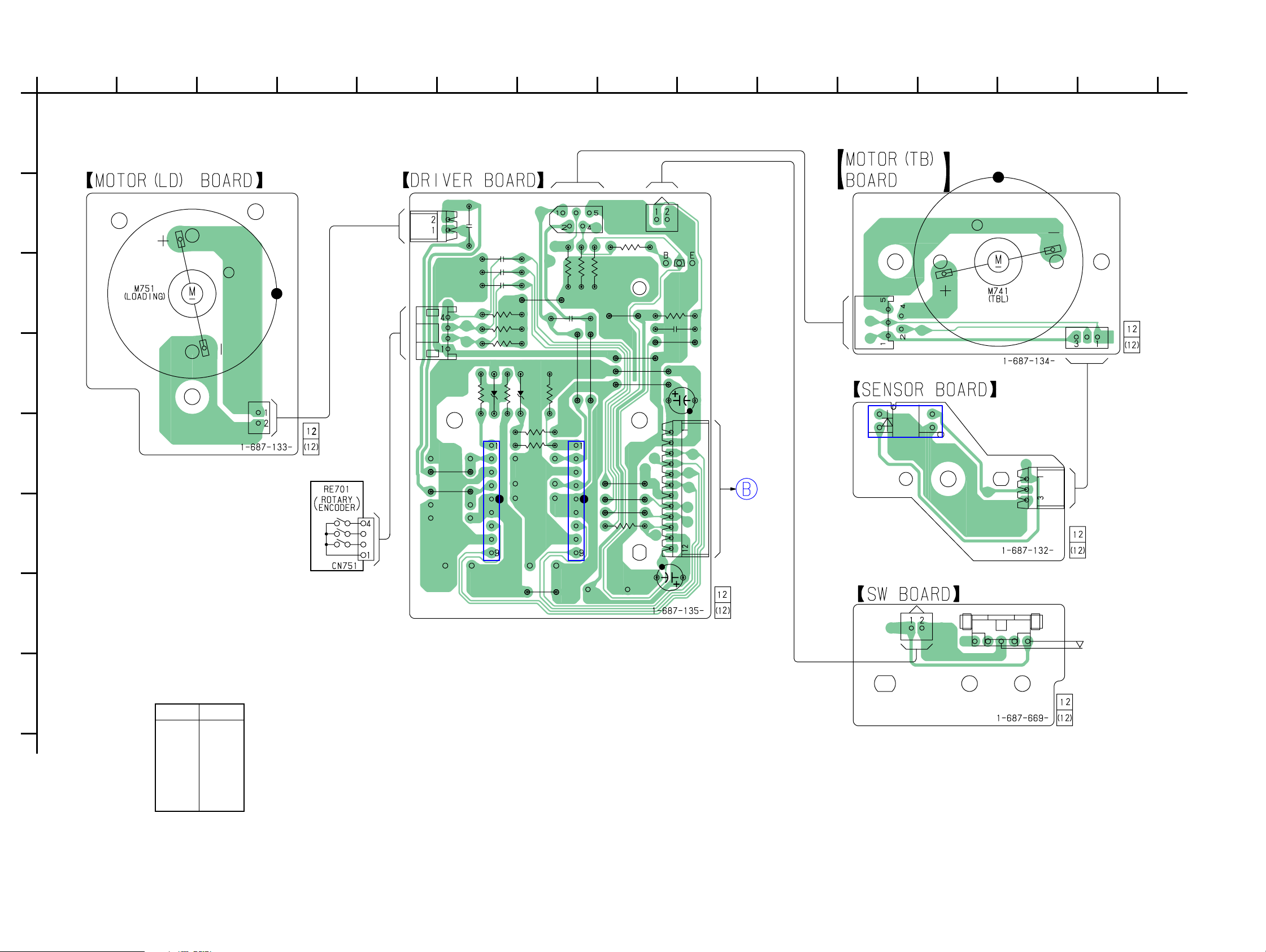
5-4. PRINTED WIRING BOARD – CD MECHANISM SECTION –
1
234567891011121314
A
B
C
D
• See page 21 for Circuit Boards Location.
CN704
C751
C737
C736
C735
JW710
R723
R722
CN703
R721
R702
D701
R701
D711
C741
R713
CN702
R735
JW709
R734
JW708
R732
R733
JW711
JW707
JW706
JW705
CN705
JW712
Q731
R751
C752
CN741
CN742
C715
E
F
G
H
• Semiconductor
Location
Ref. No. Location
D701 D-6
D711 D-7
CN721
JW713
JW714
IC701
R711
R712
JW701
IC712
JW704
JW703
JW702
R731
C731
CN701
MAIN
BOARD
CN301
(Page 30)
IC731
CN751
CN731
S751
(LEVER SW)
IC701 F-6
IC712 F-7
IC731 E-11
Q731 C-9
2828
Page 29
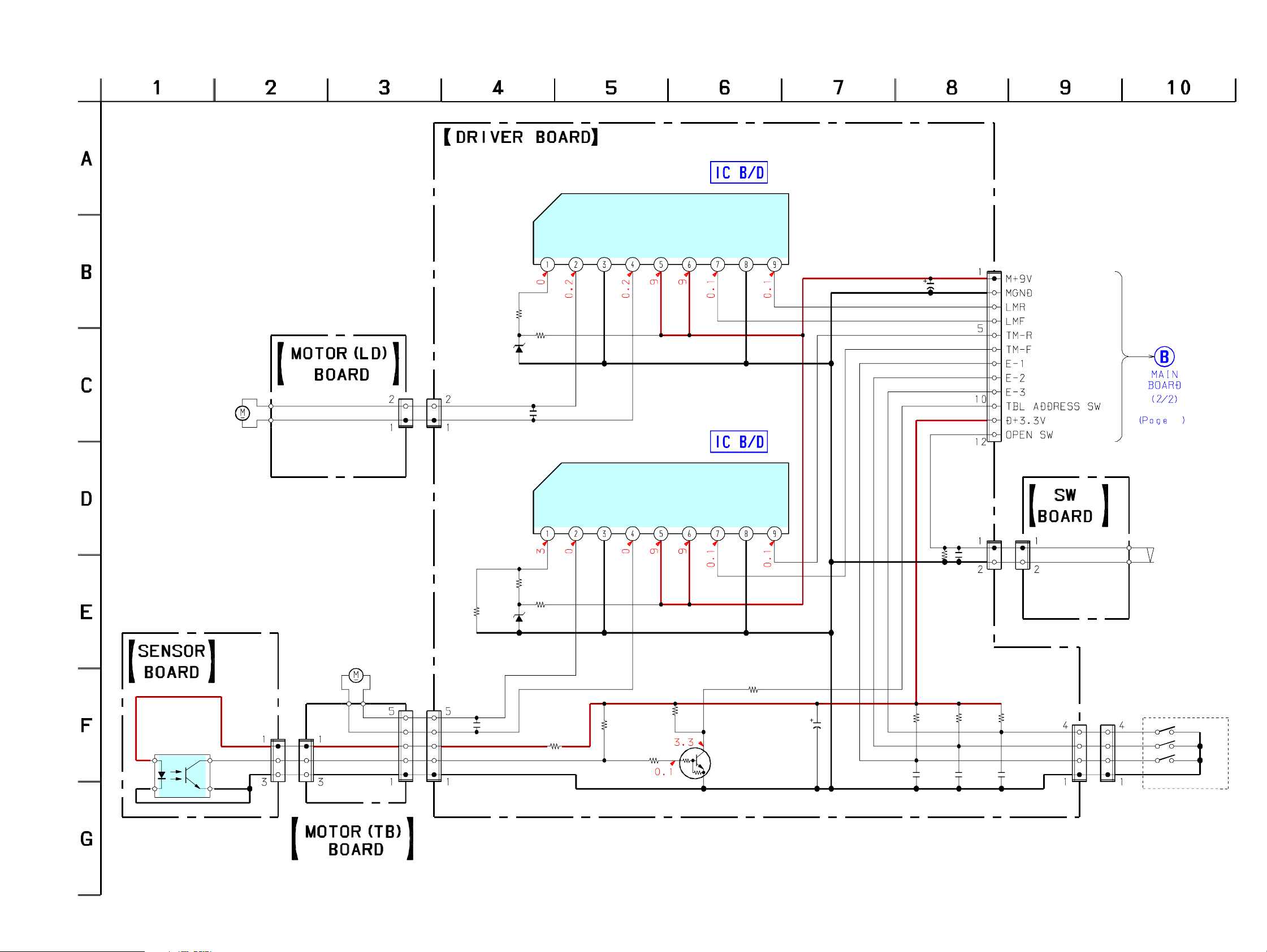
5-5. SCHEMATIC DIAGRAM – CD MECHANISM SECTION –
HCD-GX450
IC701
BA6956AN
LD MOTOR
DRIVER
M751
(LOADING)
CN721
2P
CN704
2P
R713
22k
R702
100
MTZJ-T-77-5.1A
R712
4.7k
D701
R701
470
C751
0.01
R711
1k
VREF
VREF
OUT2
OUT2
RNF
RNF
OUT1
VM
IC712
BA6956AN
TBL MOTOR
DRIVER
OUT1
VM
VCC
VCC
FIN
FIN
GND
GND
RIN
RIN
C715
100
16V
R751
4.7k
C752
0.1
CN705
2P
CN701
12P
CN301
32
S751
(LEVER SW)
CN751
2P
IC731
RPI-576
TABLE
SENSOR
CN731
3P
CN741
3P
M741
(TBL)
CN742
5P
C741
0.01
CN702
5P
D711
MTZJ-T-77-3.6B
R735
100
R734
12k
R733
1k
R732
10k
DTC114ESA
TBL ADDRES
SENS SWITCH
2929
R731
100
Q731
C731
10
50V
R721
4.7k
C735
0.1
R722
4.7k
C736
0.1
no mark : FM
R723
4.7k
C737
0.1
CN703
4P
CN751
4P
RE701
ROTARY
ENCODER
E-3
E-2
E-1
Page 30
HCD-GX450
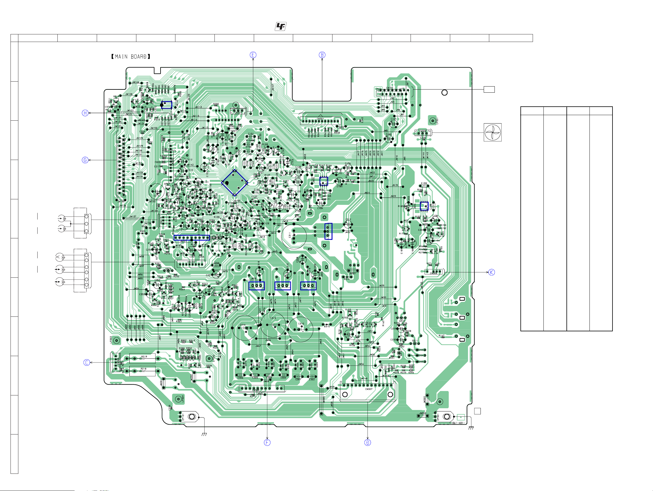
5-6. PRINTED WIRING BOARD – MAIN SECTION –
12
345678910111213
A
B
CONNECT
BOARD
CN254
(Page 33)
E
E
C
PANEL
BOARD
CN601
D
ERASE
HEAD
L CH
R CH
HP1
R CH
L CH
HP2
HE1
HRP2
HRP1
E
F
PB
HEAD
REC/PB
HEAD
(Page 37)
DECK-A
(PLAY)
DECK-B
(REC/PLAY)
28
29
1
2
3
1
2
3
4
3
4
G
H
1
• See page 21 for Circuit Boards Location.
E
IC371
10
E
E
E
E
3
1
IC201
91
E
E
1
E
E
E
E
9
1
33
6
8
E
E
3
IC101
E
E
1
GAMEJACK
(Page 33)
E
1
IC304
• : Uses unleaded solder.
BOARD
CN801
1
E
E
3
1
IC303
1
3
IC301
3
IC102
DRIVER
BOARD
CN701
(Page 28)
1
3
12
IC302
TUNER
• Semiconductor Location
Ref. No. Location
FAN
1
3
D201 I-10
D202 H-10
D203 H-11
D204 H-11
D205 I-11
D206 I-10
D207 I-10
D211 F-4
D212 G-5
D213 G-5
D214 G-5
D215 G-4
D301 I-8
D302 I-8
IC104
D303 I-8
D304 I-8
D305 I-7
D306 I-7
D307 I-7
E
D308 I-7
D309 I-7
E
D310 I-6
D311 I-6
D312 I-6
E
D313 F-8
D314 F-9
D315 H-8
1
4
SUB-WOOFER
BOARD
CN501
(Page 35)
D316 G-6
D321 H-5
D322 H-5
D324 E-4
D325 E-4
D326 F-4
E
E
E
E
E
E
E
IC101 D-6
IC102 D-8
IC104 D-11
IC201 E-5
Ref. No. Location
IC301 G-8
IC302 E-9
IC303 G-7
IC304 G-7
IC371 B-4
Q101 H-9
Q102 H-9
Q103 H-9
Q104 H-10
Q105 E-10
Q106 D-7
Q107 D-7
Q108 F-11
Q303 E-11
Q304 E-4
Q305 E-4
Q306 B-4
Q307 B-4
Q308 B-4
Q309 B-3
Q310 H-10
Q311 H-11
Q312 H-10
Q313 B-3
Q314 G-6
Q315 G-6
Q321 F-7
Q322 F-4
Q323 F-4
Q324 F-4
Q327 G-5
Q351 G-4
Q352 G-4
Q361 G-6
Q362 G-6
Q371 I-5
H/P JACK
I
BOARD
CN804
(Page 33)
5
J
K
E
(CHASSIS)
11
1
13
1
12
(CHASSIS)
TRANS
BOARD
CN907
(Page 40)
AMP
BOARD
CN441
(Page 41)
3030
Page 31

5-7. SCHEMATIC DIAGRAM – MAIN SECTION (1/2) –
R219
R217
CN309
CN308
CN307
CN306
CN314
PH-S(3P)
R216
56
C235
0.1
5P
EP101
C228
3P
0.1
Q310
2SC2001
R226
47k
13P
4P
680
56
2W
R218
680 2W
Q311
2SC2001
D203
JW
R228
R227
1k
1k
R225
4.7k
C230
C229
47
4.7
16V
50V
D202
MTZJ-13B
C216
FB202
FB203
FB204
0.1
FB201
7
0
2
D
0
3
2
R
C231
0.1
C214
1000
10V
C222
0.1
C217
0
0
0
0
D205
JW
D204
JW
5
D206
5
3
1SS355
S
S
1
R229
k
4.7k
.7
4
0.1
JW311
Q312
2SA953
R232
HCD-GX450
Q371
2SC3052
R397
10k
JW202
JW201
JW
JW
R231
10k
10k
R220
R222
22k
5.6k
R221
22k
R201
4.7k
R272
470k
C213
10 50V
C212
10 50V
D324
10EDB40
10EDB40
10EDB40
D201
1SS355
R202
10k
2.2 50V
D325
D326
R223
100k
C194
R268
10k
R270
1k
R271
10k
Q108
2SC3052
R204
R203
10k
Q305
Q304
2SA1235
2SC3052
R205
C211
4.7k
R207
R206
2.2k
R210
47k
2.2k
Q307
2SC3661
1k10k
R211R212
Q306
2SC3661
R209
10k
R208
10
50V
R269
2.2k
R184
4.7k
10k
R199
220k
R178
10k
1k
R385
4.7k
R386
22k
R192
22k
Q303
2SC3052
R387
4.7k
C198
0.22
IC104
NJM4565M
C203
10 50V
R389
4.7k
R395
22k
R396
4.7k
R388
22k
C199
0.33
R186
33k
R193
1k
R391
10k
R390
22k
R392
1k
R394 R393
1k 10k
C188
22
50V
R174
10k
Q105
2SC3052
R175
10k
C189
22
50V
C190
0.01
R189
100
C202
100 16V
R181
47k
R182
C196
33k
47
16V
R187
47k
C107
10
R102
50V10k
R101
10k
C101
1 50V
C102
1 50V
C206
2200p
C110
50V
R108
10
C111
C112
C113
C103
390
R106
330k
C114
H
C
p
0
2
2
6
1
1
C
p
0
3
3
7
1
1
C
R111
150k
C118
10
50V
R105
390
220p
C105
0.1 50V
R198
2.2k
2.2k
R197
C109 C108
1 50V
1 50V
1 50V
1 50V
R109
470k
R110
330k
R195
6.8k
C192
2.2
50V
C106
0.01 220p
R151
4.7k
10k
R152
C175
2.2 50V
R157
47k
R156
470k
R163
R165
10k
R173
10k
C178
47
16V
0.01
R103
330k
15k
R104
C104
0.1
50V
R107
15k
R281
2.2k
2.2k
R282
2.2k
R283
2.2k
R284
H
C
1
p
k
.0
1
.0
0
5
1
1
C
0
0
0
2
7
2
4
9
1
0
2
1
2
1
C
1
1
C
R
R113
330k
R194
6.8k
C191
2.2
50V
Q101
2SC3052
R154
R153
10k
10k
Q102
2SA1235
R155
R162
4.7k
2.2k
10k
R167
10k
R168
100k
1k
R141
R142
1k
p
0
3
3
1
2
1
C
R114
150k
C122
10
50V
R196
0
R164
10k
C176
10 50V
R166
10k
C179
47p
R115
1M
Q104
2SC3661
C177
22p
C180
220p
C124
100p
R158
2.2k
IC102
NJM4565M
100k
R169
C166
1 50V
C162
C164
1 50V
C165
1 50V
V
0
5
1
0
6
1
C
p
V
0
0
0
5
0
1
p
2
0
2
0
6
1
2
V
1
3
2
1
C
0
1
C
5
2
1
0
C
0
1
7
2
1
C
1 50V
BD3401KS22200p
Q103
2SC3661
10k
R159
R161
10k
0
9
3
1
C159
R
1
50V
IC101C193
V
6
V
V
1
0
6
1
1
7
4
7
0
4
0
0
1
3
9
1
8
2
C
2
1
1
C
C
R118
10k
R160
10k
C185
10
R172
50V
R170
10k
C181
R138
1k
R137
4.7k
C157
1
50V
7
4
7
.0
4
0
.0
0
3
3
1
1
3
C
1
C
R125
10k
R124
C187
100
0.01
C186
47
16V
C184
47
C183
16V
22p
R171
47p
10k
C182
220p
7
2
2
04
0
.0
.0
0
0
C152
0.0022
4
3
5
1
15
C
C
C151
0.01
R136
4.7k
C150
0.01
C149
R135
0.01
4.7k
C148
0.01
C147
R134
10 50V
4.7k
C146
0.1
C145
R133
10 50V
4.7k
C144
0.1
C143
C142
1
10
50V
50V
C141
10 50V
C140
0.068
M
C139
0.068
M
R132
4.7k
C275
47p
C138
10
50V
R176
C137
M
M
k
0
1
8
8
6
6
.0
.0
26
0
0
1
R
5
6
3
1
13
C
C
10k
50V
R177
C274
220k
47p
R127
4.7k
R128
15k
R131
220k
15k
10
Q106
2SC3052
R129
47k
R120
R121
1M
R123C134
10k0.1 M
Q107
2SC3052
47k
k
7
C132
4
47
16V
19
1
R
R116
100
R117
100
3131
Page 32

HCD-GX450
5-8. SCHEMATIC DIAGRAM – MAIN SECTION (2/2) –
Q362
2SC3052
R364
4.7k
R363
4.7k
R275
Q315
2SC3052
R322
22k
D321
1SS355
R325
4.7k
D311
D312
10EDB40
10EDB40
C306
0.1
CN303
R273
0
11P
C354
0.1
C270
10 50V
R362
R361
2.2k
10k
Q361
2SA1235
0
R321
4.7k
C321
2.2
50V
R323
4.7k
R274
10EDB40
C305
0
100 16V
D310
D316
1SS355
Q314
2SA1235
C313
2200
25V
JW305
JW
D305
10EDB40
IC303
TA7809S
C302
0.1
IC371
BU2099FV
C312
10
50V
D314
10EDB40
IC302
TA78033LS
C309
22
50V
C308
22
50V
JW301
JW
D313
11EQS04
D315
10EDB40
D301
10EDB40
D303
10EDB40
C374
47
16V
C375
0.1
R384
10k
R383
10k
R382
10k
R381
10k
R380
10k
R379
10k
R307
10k
R311
Q313
2SC3052
2SA1235
4.7k
2SC3052
R313
4.7k
1SS355
R312
C376
2.2
50V
Q308
Q309
IC301
TA78033LS
D322
22k
R306
10k
R308
2.2k
R310
10k
C311
10
50V
C310
3300
25V
C301
0.1
D302
10EDB40
D304
10EDB40
1SS355
D215
C241
1000p
R241
10
C242
0.015
0.0047
C251
47 16V
R250
R251
10k
10k
Q324
2SB1116
R245
4.7k
Q322
2SA1235
R252
0
C248
1000p
BA3126N
C249
10
50V
R246
R247
10k
R248
Q323
10k
2SC3052
D211
1SS355
Q321
2SC2001
R242
27k
C243
C244
0.015
M
L101
C246
R244
0.015
8.2k
M
C247
0.01
IC201
100
C250
47
16V
R249
47k
R243
1000p
8.2k
C245
R324
10k
C318
IC304
TA7809S
JW303
C316
2200
25V
EP301
D309
10EDB40
10EDB40
308
D
0.1
C304
C315
100
16V
JW
JW302
JW
D307
10EDB40
D306
10EDB40
C303
0.1
0.1
C371
100p
R371
100
C372
100p
R372
100
C373
R373
100p
100
R374
10k
R375
10k
R376
10k
R377
10k
R378
10k
C252
100
16V
D212
1SS355
C258
0.47
50V
R264
1k
C259
0.22 50V
R266
100k
D214
1SS355
C351
1000p
R351
R353
15k
47k
2SC3052
R356
470
R357
2.2k
C352
22 50V
R253
100
R262
C253
3.3k
0.1 50V
D213
1SS355
Q327
2SC3052
R263
1M
R265
10k
R352
100k
Q351
R354
4.7k
Q352
2SC3052
R358
100
C353
2.2
50V
C264
1000p
C265
1000p
CN112
3P
C266
1000p
C267
1000p
CN103
8P
HP1
HP2
HRP1
HRP2
HE1
R346 R345
1k 10k
R341
R342
10k
1k
22k
22k
R344
CN301
22k
R347
348
C342
R
0.1
12P
22k
R343
1k
1k
R213
R214
CN302
29P
3232
Page 33

HCD-GX450
5-9. PRINTED WIRING BOARD – PANEL COMB SECTION –
12
A
34567891011
PANE L
BOARD
CN603
(Page 37)
B
MAIN
BOARD
CN305
(Page 30)
C
• See page 21 for Circuit Boards Location.
M
PANE L
BOARD
CN605
(Page 37)
• : Uses unleaded solder .
(AMS-
HML-)
1
5
3
MASTER VOLUME
1
(AMS+
HML+)
LED610-LED615
(ILLUMINATION
LIGHT)
6
1
J
PANEL
BOARD
CN604
(Page 37)
PHONES
(CHASSIS)
1
5
MAIN
BOARD
CN309
(Page 30)
D
E
F
BD81A
BOARD
CN201
(Page 26)
• Semiconductor
Location
Ref. No. Location
LED610 B-7
LED611 B-6
(CHASSIS)
VIDEO
1
2
1
3
VIDEO
L R
AUDIO
GAME INPUT
E
MAIN
BOARD
CN314
(Page 30)
2
OUT
LED612 B-6
LED613 C-6
LED614 C-6
LED615 C-7
3333
Page 34

HCD-GX450
5-10. SCHEMATIC DIAGRAM – PANEL COMB SECTION –
CN251
CN254
9P
JW259
27P
JW254
JW252
JW
JW253
JW
JW255
JW
JW257
JW
JW256
JW
JW
FB251
JW258
JW251
JW
JW
JW261
JW
100p
C251
JW
EMI
FB252
EMI
C257
0.1
CN253
17P
0.1
0.1
470p
0.01
100p
C255
C256
C254
C252
C253
SW601
SW ESE24SV
JR801
0
CN606
R803
R804
S660
ENCORDER
VR
1/8W
R699
220
R673
22k
6P
CN802
2P
R801
10k
C801
22k
470p
C802
470p
R802
10k
C804 C803
0.22 0.22
CN801
3P
22k
LED610
SELU5223C
CN607
J804
-STP15
5P
701
R
LED611
SELU5223C
/8W
1
220
-STP15
/8W
1
R703
220
-STP15
LED612
SELU5223C
5
70
R
LED613
SELU5223C
1/8W
220
-STP15
07
7
R
LED614
SELU5223C
/8W
1
220
-STP15
09
7
R
LED615
SELU5223C
/8W
1
220
-STP15
CN805
2P
CN804
5P
C830 C831
1000p 1000p
J801
C832
0.1
W803
WIRE
J803
WIRE801
3434
Page 35

HCD-GX450
5-11. PRINTED WIRING BOARD – SUB-WOOFER SECTION –
12
A
1
B
• See page 21 for Circuit Boards Location.
• : Uses unleaded solder.
345678
MAIN
BOARD
CN306
(Page 30)
4
7
AMP
BOARD
CN443
(Page 41)
1
C
D
• Semiconductor
Location
Ref. No. Location
D501 C-3
D502 C-5
D503 C-5
D504 B-6
D505 C-8
D506 C-7
D507 C-2
E
E
E
E
E
E
IC501
CONTROL
SUB WOOFER OUT
(IMPEDANCE USE 6–16 )
IC501 D-3
Q501 D-5
Q502 C-8
Q503 C-6
Q505 C-7
Q506 C-7
Q507 D-1
3535
Page 36

HCD-GX450
5-12. SCHEMATIC DIAGRAM – SUB-WOOFER SECTION –
IC501
STK404-130S
CN501
4P
R528
1/4W
10k
D506
MTZJ-T-77-6.8B
C515
4.7
50V
2SC2785
D505
1SS133T-77
R527
1/4W
Q507
D507
1SS133T-77
R525
22k
1/4W
R526
8.2k
1/4W1M
R531
4.7k
1/4W
R530
22k
1/4W
R529
2.2k
1/4W
C503
4700p
16V
R501
47k
1/4W
C516
50V
R517
10k
1/4W
R516
100
1/2W
47
C509
100V
100
C508
220p 50V
R508
4.7k
1/2W
R509
100 1/4W FR
R505
4.7k 1/2W
C510
100V
R511
R510
0.22
0.22
5W
5W
R513
1k
1/4W
C513
0.1
C512
R514
0.1
C511
10
100V
10
R512
1/2W
22k
1/4W
10
D502
1SS133T-77
Q501
2SC1841
D503
1SS133T-77
R515
47k
1/4W
D504
R507
4.7k
C505
R504
47k
1/4W
1/4W
1k
R503
C504
22
25V
R506
1 1/4W FR
10p
50V
JW520
JW
C506
100
25V
10
JW501
JW
C502
220p
50V
1/4W
47k
R502
1/2W
C507
50V
D501
MTZJ-T77-12B
1SS133T-77
Q502
2SA1175
R518
2.2k
1/4W
R519
2.2k
1/4W
RY501
SP RELAY
12V
CN503
2P
JK501
CN502
7P
Q506
2SC2785
C514
R524
R532
47k
22k
1/4W
1/4W
Q505
100
35V
2SC2785
C517
50V
10
R533
22k
1/4W
R520
100k
1/4W
2SC2785
Q503
3636
Page 37

5-13. PRINTED WIRING BOARD – PANEL SECTION –
• See page 21 for Circuit Boards Location.
HCD-GX450
Ver. 1.1
• : Uses unleaded solder.
A
B
C
D
12
DISC 1
DISC 2
SURROUND
DISC 3
EFFECT
ON/OFF
345678910111213
CONNECT
GROOVE
BOARD
CN253
(Page 33)
*1
LC876996A type
used for IC601
EQ BQND
(CHASSIS)
1
41
45
3
1
E
3
1
IC604
45
IC603
13
E
PLAY MODE/
TUNING MODE
E
DISPLAY
1
3
4
3
5
1
IC610
ILLUMINATION
CD
11
20
10
TUNER/BAND
1
IC602
100
25 30
51
50
*1
IC601
1
35
31
30
5
10
15
20
(FLUORESCENT INDICATOR TUBE)
80
81
E
F
G
MAIN
BOARD
CN302
(Page 30)
DISC SKIP
EX-CHANGE
• Semiconductor Location
Ref. No. Location
D603 C-11
D604 C-11
D605 C-10
D607 C-10
D608 D-8
D609 D-8
D610 D-8
D611 D-8
D613 D-9
D614 C-9
D615 F-6
D616 F-6
D621 B-6
D623 B-6
D626 B-5
D630 E-4
D631 C-8
D632 C-9
IC601 C-7
ENTER
RESET EQ
P FILE
Ref. No. Location
IC602 D-11
IC603 D-9
IC604 C-8
IC610 C-12
LED601 B-11
Q601 F-6
Q602 F-7
Q603 F-6
Q604 B-9
Q605 C-8
Q610 E-8
Q611 E-7
Q612 E-7
Q613 F-7
Q614 F-8
Q615 F-8
Q616 A-9
M
ALBUM+
h
TUNING+
E
E
TAPE
MECHNISM
DECK
Attention when exchanging IC601
Original Part Repair Part
6-804-130-01 LC876996A-52S4-E 6-804-130-01 LC876996A-52S4-E
1 This IC is not compatible with 2
and 3.
6-804-440-01 LC876996A-53H2-E 6-804-440-01 LC876996A-53H2-E
or
2 6-805-469-01 LC876A96A-55D8-E
When the above IC is exchanged,
remove R789.
3 6-805-469-01 LC876A96A-55D8-E 6-805-469-01 LC876A96A-55D8-E
M
ALBUM–
E
E
EE E
1
5
6 STREAM
LED BOARD
CN607
(Page 33)
E
6
1
6 STREAM
LED BOARD
CN606
(Page 33)
X
GAME MIXING
x
TUNING-
CD SYNC
PAUSE/START
*1 IC601, R789
When IC601 is exchanged for LC876A type,
remove R789. (R789 : Location C-4)
TAPE A/B
GAME
REC
3737
Page 38

HCD-GX450
5-14. SCHEMATIC DIAGRAM – PANEL SECTION (1/2) –
220
R704
220
R706
220
CN605
CN604
CN601
R708
220
R700
220
R702
5P
R698
220
6P
JW601
JW602
10
R629
100
R690
R691
100
R692
100
R693
100
R694
100
R695
100
R696
100
R697
100
R635
100
29P
JW660
JW659
JW
JW
DTC143EKA
-T146
R628
Q610
10k
R627
10k
0.1
655
C
Q612
DTC143EKA-
T146
C644
10
16V
Q611
DTC143EKA-
T146
C604
0.1
25V
Q614
DTC143EKA-
T146 DTC143EKA-
674
JW
JW
718
JW
JW
705
JW
JW
R639
4.7k
R638
100
632
R
JW
6
62
JW
C601
22p
100
IC602
BU2099FV
JW
625
JW
JW
703
JW
C602
22p
655
JW
JW
R640
100
634
633
R
R
35
6
JW
JW
714
716
JW
JW
701
JW
C603
22p
Q615 Q613
T146
D605
1SS355TE-17
D604
1SS355TE-17
D603
1SS355TE-17
R672
10k
JW641
JW
00
1
0
0
JR609
607
608
0
JW
JR
JR
JW
JW
656
JW
DTC143EKA-
W
J
T146
R854
R641 C605
220k 4.7
R731
100
50V12k
JW811
8
65
JW
JW
220
JW
R674
15k
R663 R652 R651
22k 15k 10k
R662 R658
10k 2.2k
S630
S610S611S612
S629
R649 R648 R647 R646 R645
R650
4.7k 3.3k 2.2k 1.5k 1.5k
6.8k
S608
R660R661
4.7k6.8k
S628 S627
S607
R659
3.3k
S626
R657 R656 R655
1.5k 1.5k 1k
S624 S623 S622
R644 R643 R642
1k 680 470
R654 R653
680 470
S601S602S603S604S605S606
R675
15k
S621
R722
R721
15k
10k
S649 S648S650
R671
R720
4.7k
6.8k
S647
R668R669R670
1.5k2.2k3.3k
S645
S646
S643S644
R665
R666R667
680
1k1.5k
S642
R676R664
15k470
S641
3838
Page 39

5-15. SCHEMATIC DIAGRAM – PANEL SECTION (2/2) –
JW812
JW
R785
100
R783
100
R782
100
R781
100
R780
470
R779
100
R778
100
R777
100
R776
100
R775
100
R774
100
JR
JR617
CN603
17P
*1 R789
47K: LC876996A type used for IC601
no mount: LC876A96A type used for IC601
R719
R718
3.3k
22k
R716
22k
R717
3.3k
• See page 49 for IC PIN FUNCTION DESCRIPTION.
FL601
FL
0k
0k
0k
0k
0k
0k
0k
0k
0k
0k
100k
100k
100k
100k
10
10
10
10
10
10
10
100k
100k
100k
100k
769
R
C622
4.7
50V
R770
C620
47
35V
100
R773
R789
*
1
C643
0.1
R784
100
100
R787
D607
1SS355TE-17
C647
47
10V
C654
0.1
768
R
0.022
JW728
JW729
10k
637
R
C621
JW670
JW673
767
R
JW
10k
636
R
5
6
76
76
R
R
SELU5223C -STP15
JW724
JW
JW723
JW
JW722
JW
JW721
JW
JW706
D611
1SS355TE-17
4
76
R
JW
LED601
JW707
763
762
760
R
R761
R
R
R772
JW
JW
JW
JW
JW
708
JW
100
723
R
758
759
R
R
1k
JW
709
JW
1SS355TE-17
10
5
6
757
75
75
R
R
R
100
5
72
R
0
0
2
61
611
JR
JR
D609
0k
100k
10
10
100k
10
.7M
4
728
R
R732
470k
601
X
751
R
100
794
R
z
H
32.768K
4.7M
727
R
750
R
00
1
100
793
792
R
R
IC601
*
1
LC876996A-52S4-E
LC876996A-53H2-E
LC876A96A-55D8-E
p
22
25
C6
C610
1000
6.3V
0.1
C626
X602
10MHz
100p
C640
1SS355TE-17
100
33
R7
C611
0.1
53
52
754
7
7
R
R
R
.1
642
0
C
100
96
7
R
00
1
795
R
100
100
0
29
R73
R7
C624
18p
HCD-GX450
Ver. 1.1
0p
0p
0p
0p
0p
0p
00p
00p
00p
1
639
C
D626
100p
1
10
10
10
1
4
7
33
35
63
638
63
636
C
C
C
C
C6
C6
-17
5TE
623
D
35
SS
1
0
00
1
10
91
7
R
R788
R681
C607
220k
1000p
R680
22k
0p
00p
1
10
10
10
10
1
0
632
628
C
C629
C63
C63
C
R771
47k
D621
1SS355TE-17
k
1
1k
1k
35
734
736
7
R
R
R
C653
330p
C623
4.7
50V
1k
C618C617
1000p1000p
R621
10k
R622
1k
Q601
2SB1068TP-K
R623
10k
2SB1116-TP-LK
1SS355TE-17
R625
10k
Q603
2SB1116-TP-LK
1SS355TE-17
R712
10
R713
10
47k
4.7k
4.7k
6
60
R607
R
R605
47k
4.7k
4.7k
R608
4.7k
R790
R609
1k
CN608
22k
R611
R610
22k
10k
R797
1k
R613
R612
22k
10k
R614
22k
R615
22k
R798
1k
R616
R617
10k
22k
R799
1k
R619
R618
22k
10k
R620
22k
3P
JR624
CN610
JR621
0
D615
D616
C619
47
10V
4.7k
1
2
04
60
60
603
R6
R
R
R
CN602
13P
IC610
RPM7240-H4
0
3P
R710
10k
R711
10k
JW606
JW
R624
JW607 Q602
1k
C641
0.1
25V
R749
100k
100k
R748
100k
R747
100k
R746
100k
R745
100k
R744
100k
R743
100k
R742
100k
R741
100k
R740
100k
R739
100k
R738
R737
100k
C649
0.1
JW
JW608
R626
JW
R714
100
R715
47
*1 IC601, R789
When IC601 is exchanged for LC876A type,
remove R789.
Refer to Attention when exchanging IC601 (Page 37).
D630 R678
1SS355TE-17 100k
R677
0
C648
22
16V
WIRE806
WIRE
(CHASSIS)
D608
C608
0.01
R684
1k220k
DTC143EKA-T146
1SS355TE-17
C609
1
D610
UDZSTE
Q616
-174.3B
IC603
R863
100
R679
100
MM1574A
C646
C606
22
1
16V
Q604
2SA1175TP-HFE
R683
R786
10k
R682
10k
C612
10
C613
16V
0.1
R689
D613
4.7k
1SS355TE-17
R688
470
D631
UDZSTE
-176.8B
Q605
2SC3052F
R686
47k
47k
D614
1SS355TE-17
IC604
C615
2.2
50V
M62703ML
R687
10k
C614R685
0.1
D632
UDZSTE
-173.6B
3939
Page 40

HCD-GX450
5-16. PRINTED WIRING BOARD – TRANS SECTION –
12
3456789101112
A
B
C
POWER TRANSFORMER
(SUB)
• See page 21 for Circuit Boards Location.
3
1
• : Uses unleaded solder.
2
1
POWER TRANSFORMER
113
E
(MAIN)
D
E
F
• Semiconductor
Location
Ref. No. Location
D901 B-3
D902 B-2
D903 B-2
D904 B-2
D905 B-2
D906 C-10
D908 C-8
3
AC
IN
1
2
1
N
AMP
BOARD
CN442
(Page 41)
F
*
10
2
1
Not replaceable
*
built in transformer
MAIN
BOARD
CN303
(Page 30)
Q902 C-9
4040
Page 41

HCD-GX450
5-17. PRINTED WIRING BOARD – AMP SECTION –
12
A
B
C
• See page 21 for Circuit Boards Location.
• : Uses unleaded solder.
345678910
• Semiconductor
Location
SPEAKER
(IMPEDANCE USE 6–16 )
LR
+
+
-
-
(CHASSIS)
E
IC441
E
E
E
E
Ref. No. Location
D401 F-3
D441 D-6
D442 D-6
D443 D-2
D481 D-6
D482 D-4
D483 C-9
IC441 B-7
Q441 D-6
Q442 D-6
Q481 D-9
Q482 D-8
Q483 D-8
Q484 D-8
Q485 C-4
Q486 C-4
Q487 C-4
Q488 C-5
Q489 C-9
D
E
F
MAIN
BOARD
CN307
(Page 30)
E
1
17
13
SUB-WOOFER
BOARD
CN502
(Page 35)
3
1
E
E
E
E
(CHASSIS)
G
TRANS
BOARD
CN905
(Page 40)
(CHASSIS)
4141
Page 42

HCD-GX450
5-18. SCHEMATIC DIAGRAM – AMP POWER SECTION –
CN905
3P
F904
T8.0AL/125V
FH908 FH907
PT901
FH910
FH912
FH914
CN907
10P
Q902
2SA1932
C910
R467
33k
1/4W
Q489
2SC1841
R496
100
D
50V
7
-2
6
2
0
7
9
D
J-T
Z
T
M
D483
1SS133T-77
C488
35V
1
1
1
1
.0
.1
.1
.0
.0
.0
0
0
1
0
2
2
9
9
C
C
C441
R411
10
R413
4.7k
1/4W
R414
1/4W
TERMINAL,
4.7k
50V
EP491
EARTH
C443
1000p
C444
1000p
C442
R441
1k
R443
47k
1/4W
C492
0.01
R444
47k
1/4W
C446
100p
50V
JW442
R442
JW
10
1k
50V
R412
2.2k
1/4W
2.2k
1/4W
JW441
C445
100p
R445
0.1
0
0
0
0
6
3
5
4
2
2
2
2
2
2
9
9
9
9
9
C
C
C
C
C
JW
50V
1k
C447
22
35V
C448
35V
R446
IC441(1/2)
STK403-130
R491
22k
1/4W
22
R495
1
1/4W
FR
1k
IC441(2/2)
STK403-130
100 1/4W FR
F905
T8.0AL/125V
T3.15AL/125V
F907
T3.15AL/125V
R904
1k
R493
33k
1/4W
22
FH909
F906
R447
47k
1/4W
FH911
FH913
D908
R908
10EDB40-TB3
1 1/4W
R902
JW917
JW
C908
220
63V
R903
12k
C909
10
50V
R492
1k
1/4W
R494
2.2k
1/4W
C489
100
100V
R448
47k
1/4W
JW404
JW
C906
0.1
JW403
JW
R451
0.22
5W
R455
Q441
1k
2SC1841
R457
22k
7
R459
-7
1
T
4
47k
3
4
3
D
1
S
S
1
7
-7
2
T
4
3
4
3
D
1
S
S
1
R458
R460
22k
47k
6
Q442
5
k
4
1
2SC1841
R
R452
0.22
5W
3.3M
1/2W
C911
1000
25V
C451
0.1
C453
0.1
R453
10
1/2W
7
-7
1
T
8
4
33
D
1
S
S
1
R454
10
1/2W
C454
0.1
C452
0.1
JW909
2SC2785
CN904
2P
JW
CN906
3P
R466
R465
56k
47k
1/4W
1/4W
Q482
C481
Q481
100
2SC2785
10V
Q485
2SA1175
R481
4.7k
1/4W
R487
33k
1/4W
Q487
2SC2785
Q486
2SC2785
R488
22k
1/4W
R483
1/4W
R484
1/4W
Q484
2SC2785
CN903
2P
D903 D902
10EDB40-TB3
10EDB40-TB3
CN902
3P
TH441
TH-10K
22
R485
100k
56k
1/4W
Q483
2SC2785
C486
R482
2.2
10k
50V
1/4W
R490
4.7k
1/4W
7
-7
2
T
8
3
4
3
C487
4.7
50V
2SC2001
D
1
S
S
1
R489
4.7k
1/4W
10EDB40-TB3
D904
D905
10EDB40-TB3
R486
100k
1/4W
Q488
LK
JW910
JW902
JW
JW
SP RELAY
02
W
4
J
W
J
RY441
7
-7
T
33
1
S
RY901
RELAY U
PT902
JW903
JW
JW906
JW
L441
10 1/2W
R461
12V
10 1/2W
R462
L442
D443
1SS133T-77
R407
100
1/2W
C411
0.01
16V
D401
D10XB20
C405
3300
63V
R401
100k
C406
3300
63V
JW407
JW
EP402
TERMINAL, EARTH
R402
100k
C403
0.1
100V
C404
0.1
100V
1S
1
0
9
D
W001
2P
TERMINAL, EARTH
EP401
AC CORD U
CN441
JK441
13P
CN901
V
V
6
6
1
1
1
1
.0
.0
0
0
7
8
0
0
4
4
C
C
C402
0.01
16V
JW401
JW
CN443
CN442
3P
7P
4242
Page 43

• IC BLOCK DIAGRAMS
HCD-GX450
IC251 BA5947FM (BD81A BOARD)
CH4OUTR
CH4OUTF
CH3OUTF
CH3OUTR
POWVCC
MUTE
GND
GND
PREGND
CH3RIN
CH3FIN
CH4IN
CH4CAPA
OUTVREF
DPOUT
TREVCC
D
19
D
20
D
21
D
22
POW
VCC
23
(ch3, 4)
50k 50k
24
25
26
27
28
CT
R
29
F
30
100k
31
PIN3
32
10k
50k
33
34
Pre
35
Vcc
36
NC
R
MUTE
INTER
FACE
10k
19k
F
LEVEL
SHIFT
Vref
50k
POW
VCC
PIN26
6.5k
50k
50k 50k
Vref
INTER
F
FACE
D
CH1PUTF
18
D
CH1OUTR
17
D
CH2OUTF
16
D
CH2OUTR
15
POW
VCC
(ch1, 2)
F
R
INTER
FACE
R
F
SW
POWVCC
14
CNF4
13
12
GND
C-M
11
10
C-P
9
VG
R
8
CH2RIN
F
7
CH2FIN
CH1RIN
6
5
CH1FIN
SW
4
3
OPIN+
2
OPIN-
NC
1
IC701, 712 BA6956AN (DRIVER BOARD)
TSD
CONTROL LOGIC
1 2 3 4 5 6 7 8 9
VREF
OUT2
RNF
OUT1
VM
VCC
FIN
GND
RIN
43
Page 44

HCD-GX450
IC301 TC94A34FG-002 (BD81A BOARD)
RAS
CAS
OE
BUCK
CCE
AD12
AD11
VDDM
SRMSTB
VDDT
ALU
MAC
CKI
VDD
A2 A3
A0 A1
WE
PIO7
33
34
35
36
37
38
39
40
41
42
General
In/Output Port
SRAM/
DRAM I/F
I/F
CDP Cont
PIO5
PIO6
SRAM I/F
2sets
Address Calc.
CROM
CRAM
ERAM
4k word
4k word
2k word
PIO4
register
C-Pointer
register
Y-Pointer
register
X-Pointer
PIO3
1Mbit
SRAM
X-Bus
PIO2
Y-Bus
PIO1
2526272829303132 1718192021222324
register
Y0 • Y1 • Y2
XO • X1 • X2
PIO0
VSS
AX AY
MX MY MZ
SFSY
TXO
DIT
round & limit round & limit
SBSY
I/F
Sub code
Audio I/F
DATA
LRCKIA
16
15
BCKIA
SDI0
14
LRCKO
13
12
BCKO
11
SDO0
10
VSS
9
VDDT
MIACK
8
MICK
7
AD10
AD9
AD8
AD7
AD6
AD5
YRAM
AD2
4k word
XRAM
4k word
AD1
AD0
54
Bus
Switch
VSS
VDD
VC0
MCU. I/F
Control
Program
POM
CKO
Timing
Generator
5857555351
VDDX
PRAM
XO
Decoder
Instruction
61 62 63 646059565250
XI
VSSP
TEST
MIMD
VSSX
43
44
45
46
47
48
49
AD4
AD3
VCOI
6
5
4
3
2
1
MIDIO
MILP
MICS
STANBY
RESET
VDDP
44
Page 45

IC101 BD3401KS2 (MAIN BOARD)
HCD-GX450
TNF2
TNF1
SUR1
SUR2
LINEOUT2
LINEOUT1
SAOUT2
SAOUT1
CAP
MIC
GAME L
GAME R
TUNER L
TUNER R
VIN2
TONE OUT1
37
BBIN1
VIN1
36 35 34
+
-
BNF1
MNF2
MOUT2
47
48
49
50
MNF1
MOUT1
46 45 44
BASS MIDDLE TREBLE
BOUT1
43 42 41
BOUT2
BNF2
40 39 38
TONE OUT2
AMS OUT
+
51
SURROUND
52
+
53
-
+
54
-
55
56
57
58
59
60
61
62
ATT
+
+
INPUT
SELECTOR
SOFT
ATT
SWITCH
+
+
BASS MIDDLE TREBLE
BUFFER
MIX
MIC MIX
VOCAL FADER
+
+
+
-
-
+
-
G
fc=100HZ
-
+
+
-
BBNF1
+
-
+
0
Di-LIMITER
VOLOUT1
33
+
VOLOUT2
32
-
BBNF2
31
BBIN2
30
LF1
29
LF2
f
28
LF3
27
LF4
26
+
SWOUT
25
-
FILTER
24
1/2 Vcc
23
Vcc
22
GND
21
VDD
20
SI
19
DIGITAL
-
RECOUT1
16
RECNF1
CONTROL
SC
18
ALC
17
MD L
63
MD R
64
CD R
3
456
TAPE L
TAPE R
12
CD L
PBNF2
-
-
+
+
PBOUT2
-
+
+
7
PBOUT1
ALC
ALC
RECNF2
-
+
14
+
15
RECOUT2
-
8
910111213
PBNF1
TAPE A1
TAPE A2
TAPE B1
TAPE B2
IC371 BU2099FV (MAIN BOARD)
IC201 BA3126N (MAIN BOARD)
1
REC SW1
2 3
GND
PB SW1
4
CONT
5
6
GND
7
CC
V
PB SW2
9
8
GND
REC SW2
IC602 BU2099FV (PANEL BOARD)
DD
OE
V
1
SS
V
2
N.C.
SO
Q11
181920
CONTOROL
3
DATA
16 15
17
12BIT SHIFT REGESTER
CIRCUIT
OUTPUT BUFFER (Open Drain)
L. P. F
4
CLOCK
Q10
12BIT STORAGE
RAGESTER
5 6 7 8
LCK
Q8
Q9
Q0
Q7
13
14
Q1
Q2
Q5
Q6
12
11
9
10
Q3
Q4
45
Page 46

HCD-GX450
5-19. IC PIN FUNCTION DESCRIPTION
• IC101 CXD3059AR (RF AMP) (BD81A BOARD)
Pin No
1
2
3
4
5
6
7
8
9
10
11
12
13
14
15
16
17
18
19
20
21
22
23
24
25
26
27
28
29
30
31
32
33
34
35
36
37
38
39
40
41
42
43
44
45
46
47
48
49
Pin Name
MIRR
DFCT
FOK
VSS
LOCK
MDP
SSTP
IOVSS1
SFDR
SRDR
TFDR
TRDR
FFDR
FRDR
IOVDD1
AVDD0
AVSS0
NC
E
F
TEI
TEO
FEI
FEO
VC
A
B
C
D
NC
AVDD4
RFDCO
PDSENS
AC_SUM
EQ_IN
LD
PD
NC
RFC
AVSS4
RFACO
RFACI
AVDD3
BIAS
ASYI
ASYO
VPCO
VCTL
AVSS3
I/O
I/O
Mirror signal input/output (Not used)
I/O
Defect signal input/output (Not used)
I/O
Focus OK signal input/output (Not used)
—
Internal digital ground
GFS is sampled at 460Hz; when GFS is high , this pin outputs a high signal
I/O
If GFS is low eight consecutive
O
Spindle motor servo control output
I
Disk innermost detection signal input
—
I/O digital ground
O
Sled drive output
O
Sled drive output
O
Tracking drive output
O
Tracking drive output
O
Focus drive output
O
Focus drive output
—
I/O digital power supply
—
Analog power supply
—
Analog ground
—
Not used
I
E signal input
I
F signal input
I
Tracking error signal input to DSSP block
O
Tracking error signal output from RF amplifier block
I
Focus error signal input to DSSP block
O
Focus error signal output from RF amplifier block
I/O
Center voltage output from RF amplifier block
I
A signal input
I
B signal input
I
C signal input
I
D signal input
—
Not used
—
Analog power supply
O
RFDC signal output (Not used)
I
Reference voltage pin for PD
O
RFAC summing amplifier output
I
Equalizer circuit input
O
APC amplifier output
I
APC amplifier input
—
Not used
I
Equalizer cut-off frequency adjustment pin
—
Analog ground
O
RFAC signal output
I
RFAC signal input or EFM signal input
—
Analog power supply
I
Asymmetry circuit constant current input
I
Asymmetry comparator voltage input
O
EFM full-swing output (Low = VSS, High = VDD)
O
Wide-band EFM PLL charge pump output
I
Wide-band EFM PLL VCO2 control voltage input
—
Analog ground
Description
46
Page 47

HCD-GX450
Pin No.
50
51
52
53
54
55
56
57
58
59
60
61
62
63
64
65
66
67
68
69
70
71
72
73
74
75
76
77
78
79
80
81
82
83
84
85
86
87
88
89
90
91
92
93
94
95
96
97
Pin Name
CLTV
FILO
FILI
PCO
AVDD5
DDVROUT
DDVRSEN
AVSS5
DDCR
NC
BCKI
PCMDI
LRCKl
LRCK
VSS
PCMD
BCK
VDD
EMPH
EMPHI
IOVDD2
DOUT
TEST
TES1
IOVss2
NC
XVSS
XTAO
XTAI
XVDD
AVDD1
AOUT1
VREFL
AVSS1
AVSS2
VREFR
AOUT2
AVDD2
NC
IOVDD0
RMUT
LMUT
NC
XTSL
IOVSS0
XTACN
SQSO
SQCK
I/O
I
Multiplier VCO1 control voltage input
O
Master PLL (slave = digital PLL) filter output
I
Master PLL filter input
O
Master PLL charge pump output
—
Analog power supply
O
DC/DC converter output
I
DC/DC converter output voltage monitor pin
—
Analog ground
I
DC/DC converter reset pin
—
Not used
I
D/A interface bit clock input
I
D/A interface serial data input (2’s COMP, MSB first)
I
D/A interface LR clock input
O
D/A interface LR clock output f = Fs
—
Internal digital ground
O
D/A interface serial data output (2’s COMP, MSB first)
O
D/A interface bit clock output
—
Internal digital power supply
O
High when the playback disc has emphasis, low it has not
I
High when de-emphasis is ON, low when input OFF
—
I/O digital power supply
O
Digital Out output
I
Test pin Normally ground
I
Test pin Normally ground
—
I/O digital ground
—
Not used
—
Master clock ground
O
Crystal oscillation circuit output
I
Crystal oscillation circuit input
—
Master clock power supply
—
Analog power supply
O
Lch analog output
O
Lch reference voltage
—
Analog ground
—
Analog ground
O
Rch reference voltage
O
Rch analog output
—
Analog power supply
—
Not used
—
I/O digital power supply
O
Rch “0” detection flag (Not used)
O
Lch “0” detection flag (Not used)
—
Not used
I
Crystal selection input (Not used)
—
I/O digital ground
Oscillation circuit control
I
Self-oscillation when high, oscillation stop when low
Subcode Q 80-bit and PCM peak and level data output
O
CD TEXT data output
I
SQSO readout clock input
Description
47
Page 48

HCD-GX450
Pin No.
98
99
100
101
102
103
104
105
106
107
108
109
110
111
112
113
114
115
116
117
118
119
120
Pin Name
SBSO
EXCK
XRST
SYSM
D A TA
VSS
XLAT
CLOCK
VDD
SENS
SCLK
ATSK
WFCK
XUGF
XPCK
GFS
C2PO
SCOR
VDD
C4M
WDCK
COUT
NC
I/O
O
Subcode P to W serial output
I
SBSO readout clock input
I
System reset Reset when low
I
Mute input Muted when high
I
Serial data input from CPU
—
Internal digital ground
I
Latch input from CPU The serial data is latched at the falling edge
I
Serial data transfer clock input from CPU
—
Internal digital power supply
O
SENS output to CPU
I
SENS serial data readout clock input
I/O
Anti-shock input/output
O
WFCK output (Not used)
O
XUGF output (Not used)
O
XPCK output (Not used)
O
GFS output (Not used)
O
C2PO output (Not used)
O
High output when the subcode sync, S0 or S1, is detected
—
Internal digital power supply
O
4 2336MHz output (Not used)
O
Word clock output f = 2Fs (Not used)
I/O
Track number count signal input/output (Not used)
—
Not used
Description
48
Page 49

• IC601 LC876996A-52S4-E (SYSTEM CONTROLLER) (PANEL BOARD)
HCD-GX450
Pin No
1
2
3
4
5
6
7
8
9
10
11
12
13
14
15
16
17
18
19
20
21
22
23
24
25
26
27
28
29
30
31
32
33
34
35
36
37
38
39
40
41
42
43
44
45
46
47
48
49
50
Pin Name
O-MP3 CS
O-MP3 LP MOTER
I-MP3 ACK SOL-B
O-MP3 REQ SOL-A
I-SCOR
O-MP3 RESET
I-BU1924 DATA
I-BU1924 CLK
I-VOLUME-IN1
I-VOLUME-IN2
RESET
I-XT1
I-XT2
VSS1
CF1
CF2
VDD1
I-PROTECT
WFR/HP/MIC-IN
I-CD ENCODER
I-CD OPEN/CLOSE
I-T APE A START
I-TAPE B START
I-STREAM/VACS
I-KEY 3
I-KEY 2
I-KEY 1
I-SIRDS-IN
I-AC CUT
G13
G12
G11
G10
G9
G8
G7
G6
G5
G4
G3
G2
G1
S1
S2
S3
VDD3
S4
S5
S6
S7/METER-SW1
I/O
O
CS output to CD Digital Processor
O
LP output to CD Digital Processor and Motor signal output
I
ACK input from CD Digital Processor and Motor signal input
O
REQ output to CD Digital Processor and Motor signal output
I
CD Scor input
O
RESET output to CD Digital Processor
I
Data input(Not used)
I
Clock input(Not used)
I
Volume signal input from the encoder
I
Volume signal input from the encoder
I
Reset input
I
Connection for input a crystal resonator
O
Connection for input a crystal resonator
—
Ground
I
Connection for input a ceramic resonator
O
Connection for input a ceramic resonator
—
Power supply
I
Power amplifier circuit protection signal input
I
SubWoofer or Headphone detection signal input
I
Signal input from the CD encoder
I
CD tray open switch signal input
I
TAPE A switches signal input
I
TAPE B switches signal input
I
Stream/Vacs signal input
I
Function key input
I
Function key input
I
Function key input
I
Data input from the remote contorol receiver
I
Power down signal input
O
FL tube grid signal output
O
FL tube grid signal output
O
FL tube grid signal output
O
FL tube grid signal output
O
FL tube grid signal output
O
FL tube grid signal output
O
FL tube grid signal output
O
FL tube grid signal output
O
FL tube grid signal output
O
FL tube grid signal output
O
FL tube grid signal output
O
FL tube grid signal output
O
FL tube grid signal output
O
FL tube segment signal output
O
FL tube segment signal output
O
FL tube segment signal output
—
Power supply
O
FL tube segment signal output
O
FL tube segment signal output
O
FL tube segment signal output
O
FL tube segment signal output
Description
49
Page 50

HCD-GX450
Pin No
51
52
S8/METER-SW2
53
S9/METER-SW3
54
55
56
57
58
59
60
61
62
63
64
65
66
I-SPEC/MODE/METER
67
68
69
70
71
72
73
74
75
76
77
78
79
80
81
82
83
84
85
86
87
88
89
90
91
92
93
94
95
96
97
98
99
100
I-TUNED-IN
I-STEREO-IN
I-REEL-A-IN
I-REEL-B-IN
I-CD Num Senser
O-POWER-RELAY
O-SYSTEM-MUTE
O-POWER-LED
STREAM-LED6 SOLB
STREAM-LED5 SOLA
STREAM-LED4 MOTOR
STREAM-LED3 MP3-STB
STREAM-LED2
STREAM-LED1
I-LC72121 DI
O-LC72121 CE
O-LC72121/BU2099FV DO
O-LC72121/BU2099FV CLK
O-BU2099FV LCH
O-BD3401 CLK
O-BD3401 DATA
O-XRES(RESET)
O-XLT(CD-LAT)
O-CD-DATA
O-MP3-CLK
Pin Name
-VPP
S10/SW1
S11/SW2
S12/SW3
S13/SW4
S14/SW5
S15/SW6
S16/SW7
S17/SW8
S18/SW9
S19/SW10
S20
S21
I-ASM-IN
VDD4
VSS2
VDD2
O-XTCN
I-SENS
O-CD-CLK
O-MP3-DO
I-MP3-DI
I/O
—
Power supply (-)
O
FL tube segment signal output
O
FL tube segment signal output
O
FL tube segment signal output
O
FL tube segment signal output
O
FL tube segment signal output
O
FL tube segment signal output
O
FL tube segment signal output
O
FL tube segment signal output
O
FL tube segment signal output
O
FL tube segment signal output
O
FL tube segment signal output
O
FL tube segment signal output
O
FL tube segment signal output
O
FL tube segment signal output
I
METER swich input
I
Tuning a frequency signal input
I
Stereo tuning signal input
I
ASM signal input
I
A deck photo sensor signal input
I
B deck photo sensor signal input
—
Power supply
O
Table address sensor swich signal input
O
POWER RELAY control output
O
System muting signal output
O
POWER LED control signal output
O
Illumination LED control signal output
O
Illumination LED control signal output
O
Illumination LED control signal output
O
Illumination LED control signal output
O
Illumination LED control signal output
O
Illumination LED control signal output
I
Data input from Tuner
O
Chip select output to Tuner
O
Data input from Tuner and SP Driver
O
Clock output to Tuner and SP Driver
O
LCH output to SP Driver
O
Clock output to Sound Processor
—
Ground
—
Power supply
O
Data output toSound Processor
O
CD xtcn signal output
O
CD reset signal output
O
CD xlt signal output
O
CD data output
I
CD sens input
O
CD clk output
O
Clock output to CD Digital Processor
I
Data input from CD Digital Processor
O
Clock output to CD Digital Processor
Description
50
Page 51

NOTE:
• -XX, -X mean standardized parts, so they may
have some differences from the original one.
• Items marked “*” are not stocked since they
are seldom required for routine service. Some
delay should be anticipated when ordering these
items.
6-1. MAIN SECTION
SECTION 6
EXPLODED VIEWS
• The mechanical parts with no reference number
in the exploded views are not supplied.
•Abbreviation
CND : Canadian model
HCD-GX450
The components identified by mark 0 or
dotted line with mark 0 are critical for safety.
Replace only with part number specified.
Les composants identifiés par une marque
0 sont critiques pour la sécurité.
Ne les remplacer que par une pièce portant
le numéro spécifié.
#1
5
1
1
#1
4
#1
b
not
3
not
supplied
supplied
#1
2
a
#1
CD mechanism deck section-1
PT902
10
not
supplied
7
not
supplied
b
#1
#1
#1
#1
#1
#1
#1
8
not
supplied
9
#1
#1
#2
not
supplied
a
1
front panel
section
Main board section
not
supplied
#2
#1
12
1
#2
Ref. No. Part No. Description Remarks Ref. No. Part No. Description Remarks
1 3-363-099-31 SCREW (CASE 3 TP2)
2 4-245-183-61 COVER (SIDE-L) (US)
2 4-245-183-71 COVER (SIDE-L) (CND)
3 4-252-196-21 DOOR, CD
4 3-038-018-01 EMBLEM, SONY
5 4-244-849-61 COVER (TOP) (US)
5 4-244-849-71 COVER (TOP) (CND)
7 1-763-117-13 FAN, DC
8 1-769-940-11 WIRE (FLAT TYPE) (11 CORE)
9 1-693-631-12 TUNER (FM/AM)
10 1-400-285-11 F-BEAD, E2515 MRT
12 4-245-184-61 COVER (SIDE-R) (US)
12 4-245-184-71 COVER (SIDE-R) (CND)
0 PT902 X-4956-292-1 TRANS ASSY, SUB
#1 7-685-647-79 SCREW +BVTP 3X10 TYPE2 IT-3
#2 7-685-646-79 SCREW +BVTP 3X8 TYPE2 IT-3
51
Page 52

HCD-GX450
d
6-2. FRONT PANEL SECTION
54
not supplied
57
not supplied
71
58
56
70
not supplied
59
not supplied
55
61
72
62
63
not supplied
a
68
64
54
not
supplied
59
65
not supplie
66
67
54
not supplied
not supplied
not supplied
not supplied
53
54
52
53
not supplied
not supplied
not supplied
54
69
not supplied
51
a
not supplied
Ref. No. Part No. Description Remarks Ref. No. Part No. Description Remarks
51 4-252-202-01 DOOR (B), CASS
52 4-252-201-01 DOOR (A), CASS
53 4-238-631-01 TAPE SPRING
54 4-951-620-01 SCREW (2.6X8), +BVTP
55 4-252-207-11 BUTTON, FF/ALBUM+
56 4-252-208-11 BUTTON, FR/ALBUM57 4-252-214-01 KNOB, VOLUME
58 X-4956-295-1 RING ASSY, KNOB
59 4-224-104-41 DAMPER
60 4-252-198-01 WINDOW, DISPLAY
63 4-252-195-21 PANEL, FRONT (US)
63 4-252-195-31 PANEL, FRONT (CND)
64 1-769-975-11 WIRE (FLAT TYPE) (13 CORE)
65 1-773-048-11 WIRE (FLAT TYPE) (17 CORE)
66 4-231-841-01 SPRING (HEART CAM-B)
67 4-231-825-01 CAM (B), HEART
68 4-225-252-01 CUSHION (FOOT)
69 1-796-485-51 DECK, MECHANICAL (CWM43FF-05)
70 4-252-200-01 BUTTON COVER
71 4-252-206-01 BUTTON, STOP
61 4-231-824-01 CAM (A), HEART
62 4-231-836-01 SPRING (HEART CAM-A)
52
72 4-252-205-01 BUTTON, PLAY
Page 53

6-3. MAIN BOARD SECTION
HCD-GX450
#2
108
not supplied
F904
F905
101
F906
108
F907
107
PT901
101
#4
102
not supplied
#3
not supplied
107
103
104
105
106
not supplied
#2
Ref. No. Part No. Description Remarks Ref. No. Part No. Description Remarks
101 4-242-527-01 S-SCREW, ITC+4-8 R
102 A-4750-756-A AMP BOARD, COMPLETE
0 103 1-783-531-11 CORD, POWER
* 104 3-703-244-00 BUSHING (2104), CORD
105 4-988-533-01 HOLDER, PWB
106 A-4750-741-A MAIN BOARD, COMPLETE
107 4-242-539-01 BVIT 3B +3-8R W/O SLOT
108 3-905-609-41 SCREW (TRANSISTOR)
0 F904 1-576-537-11 FUSE, GLASS TUBE (DIA.5) (T8.0AL/125V)
0 F905 1-576-537-11 FUSE, GLASS TUBE (DIA.5) (T8.0AL/125V)
0 F906 1-533-451-11 FUSE, GLASS TUBE (DIA. 5) (T3.15AL/125V)
0 F907 1-533-451-11 FUSE, GLASS TUBE (DIA. 5) (T3.15AL/125V)
0 PT901 1-443-254-11 TRANSFORMER, POWER
#2 7-685-646-79 SCREW +BVTP 3X8 TYPE2 IT-3
#3 7-685-872-09 SCREW +BVTT 3X8 (S)
#4 7-685-649-79 SCREW +BVTP 3X14 TYPE2 IT-3
The components identified by
mark 0 or dotted line with mark
0 are critical for safety.
Replace only with part number
specified.
Les composants identifiés par
une marque 0 sont cr itiques
pour la sécurité.
Ne les remplacer que par une
pièce portant le numéro spécifié.
53
Page 54

HCD-GX450
2
6-4. CD MECHANISM DECK SECTION -1 (CDM74-F1BD81)
156
162
155
156
157
158
154
155
156
157
158
153
151
161
151
159
164
160
166
163
164
165
M741
152
CD mechanism deck section-
Ref. No. Part No. Description Remarks Ref. No. Part No. Description Remarks
151 4-218-253-21 SCREW (M2.6), +BTTP
152 1-776-182-11 WIRE (FLAT TYPE) (5 CORE)
153 1-687-134-12 MOTOR (TB) BOARD
154 4-243-815-01 TABLE (LOADING)
155 4-245-571-02 GEAR (STOPPER)
156 4-218-252-61 SCREW (+PTPWH M2.6), FLOATING
157 4-245-570-01 GEAR (JOINT)
158 4-245-572-01 BUSHING (GEAR)
159 1-687-132-12 SENSOR BOARD
160 4-243-820-01 GEAR (TABLE)
161 4-243-819-01 GEAR (GENEVA)
162 4-243-816-01 TRAY
163 4-243-823-01 BELT (TABLE)
164 4-985-672-01 SCREW (+PTPWH M2.6), FLOATING
165 4-243-821-01 PULLEY (TABLE)
166 3-231-598-01 SHEET (BA)
M741 A-4723-963-A MOTOR ASSY, TABLE
54
Page 55

6-5. CD MECHANISM DECK SECTION -2 (CDM74-F1BD81)
HCD-GX450
208
M751
211
212
210
RE701
202
207
213
206
214
205
204
216
205
215
not supplied
232
203
202
205
205
217
230
202
233
231
218
201
219
222
223
224
225
228
not supplied
229
222
232
222
223
224
220
225
205
205
223
222
223
205
226
227
Ref. No. Part No. Description Remarks Ref. No. Part No. Description Remarks
201 1-687-135-12 DRIVER BOARD
202 4-218-253-31 SCREW (M2.6), +BTTP
203 1-687-669-12 SW BOARD
204 4-244-034-01 BELT (LOADING)
205 4-218-252-61 SCREW (+PTPWH M2.6), FLOATING
206 4-225-844-01 GEAR (LOADING A)
207 4-224-613-01 GEAR (SHAFT)
208 1-687-133-12 MOTOR (LD) BOARD
210 4-244-108-01 GEAR, SWING
211 4-224-609-01 GEAR (LOADING C)
212 4-224-608-01 COLLAR, SWING
213 3-016-533-11 WASHER (FR), STOPPER
214 4-224-611-01 GEAR (LOADING B)
215 4-224-606-01 GEAR (RV)
216 4-243-818-01 GEAR (U/D)
217 4-243-822-02 LEVER (LIFTER)
218 X-4955-707-2 PULLEY (A5) ASSY, CHUCKING
219 4-231-189-01 PULLEY (B), CHUCKING
220 X-4955-536-1 HOLDER (213) ASSY
222 4-277-549-11 INSULATOR
223 4-277-045-31 SPRING (INSULATOR), COIL
224 4-231-151-01 STOPPER (BU)
225 4-218-253-31 SCREW (M2.6), +BTTP
226 1-827-992-11 WIRE (FLAT TYPE) (16 CORE)
227 1-775-251-11 WIRE (FLAT TYPE) (27 CORE)
228 A-4751-431-A BD81A BOARD, COMPLETE
0 229 8-820-244-01 OPTICAL PICK-UP KSM-215DCP/C2NP
230 1-471-035-11 MAGNET ASSY
231 4-243-817-11 CHASSIS
232 4-951-620-01 SCREW (2.6X8), +BVTP
233 1-469-854-11 CORE, FERRITE
M751 A-4736-655-A MOTOR ASSY, LOADING
RE701 1-477-680-12 ENCODER, ROTARY
The components identified by
mark 0 or dotted line with mark
0 are critical for safety.
Replace only with part number
specified.
Les composants identifiés par
une marque 0 sont cr itiques
pour la sécurité.
Ne les remplacer que par une
pièce portant le numéro spécifié.
55
Page 56

HCD-GX450
SECTION 7
6 STREAM LED AMP
NOTE:
• Due to standardization, replacements in the
parts list may be different from the parts
specified in the diagrams or the components
used on the set.
• -XX, -X mean standardized parts, so they
may have some difference from the original
one.
• Items marked “*” are not stocked since they
are seldom required for routine service.
Some delay should be anticipated when
ordering these items.
• CAPACITORS:
uF: µF
Ref. No. Part No. Description Remarks Ref. No. Part No. Description Remarks
6 STREAM LED BOARD
*******************
< DIODE >
LED610 6-500-809-01 DIODE SELU5223C-STP15
LED611 6-500-809-01 DIODE SELU5223C-STP15
LED612 6-500-809-01 DIODE SELU5223C-STP15
LED613 6-500-809-01 DIODE SELU5223C-STP15
LED614 6-500-809-01 DIODE SELU5223C-STP15
LED615 6-500-809-01 DIODE SELU5223C-STP15
< RESISTOR >
R673 1-216-837-11 METAL CHIP 22K 5% 1/10W
R699 1-216-182-00 RES-CHIP 220 5% 1/8W
R701 1-216-182-00 RES-CHIP 220 5% 1/8W
R703 1-216-182-00 RES-CHIP 220 5% 1/8W
R705 1-216-182-00 RES-CHIP 220 5% 1/8W
R707 1-216-182-00 RES-CHIP 220 5% 1/8W
R709 1-216-182-00 RES-CHIP 220 5% 1/8W
< SWITCH >
ELECTRICAL PARTS LIST
• COILS
uH: µH
• RESISTORS
All resistors are in ohms.
METAL: metal-film resistor
METAL OXIDE: Metal Oxide-film resistor
F: nonflammable
• SEMICONDUCTORS
In each case, u: µ, for example:
uA...: µA... , uPA... , µPA... ,
uPB... , µPB... , uPC... , µPC... ,
uPD..., µPD...
C443 1-162-294-31 CERAMIC 0.001uF 10% 50V
C444 1-162-294-31 CERAMIC 0.001uF 10% 50V
C445 1-162-282-31 CERAMIC 100pF 10.00% 50V
C446 1-162-282-31 CERAMIC 100pF 10.00% 50V
C447 1-126-965-11 ELECT 22uF 20.00% 35V
(ILLUMINATION LIGHT)
(ILLUMINATION LIGHT)
(ILLUMINATION LIGHT)
(ILLUMINATION LIGHT)
(ILLUMINATION LIGHT)
(ILLUMINATION LIGHT)
C448 1-126-965-11 ELECT 22uF 20.00% 35V
C451 1-136-497-81 FILM 0.1uF 5.00% 50V
C452 1-136-497-81 FILM 0.1uF 5.00% 50V
C453 1-136-497-81 FILM 0.1uF 5.00% 50V
C454 1-136-497-81 FILM 0.1uF 5.00% 50V
C481 1-104-658-91 ELECT 100uF 20.00% 10V
C486 1-126-961-11 ELECT 2.2uF 20.00% 50V
C487 1-126-963-11 ELECT 4.7uF 20.00% 50V
C488 1-126-965-11 ELECT 22uF 20.00% 35V
C489 1-128-563-11 ELECT 100uF 20.00% 100V
C492 1-162-306-11 CERAMIC 0.01uF 30.00% 16V
CN441 1-778-981-21 CONNECTOR, BOARD TO BOARD 13P
D401 6-500-360-01 DIODE D10XB20
D441 8-719-991-33 DIODE 1SS133T-77
D442 8-719-991-33 DIODE 1SS133T-77
D443 8-719-991-33 DIODE 1SS133T-77
D481 8-719-991-33 DIODE 1SS133T-77
When indicating parts by reference number,
please include the board name.
The components identified by mark 0 or
dotted line with mark 0 are critical for safety.
Replace only with part number specified.
Les composants identifiés par une marque
0 sont critiques pour la sécurité.
Ne les remplacer que par une pièce portant
le numéro spécifié.
< CONNECTOR >
< DIODE >
S660 1-418-632-11 ENCODER, ROTARY (MASTER VOLUME)
SW601 1-786-289-11 SWITCH, DETECTION
************************************************************
A-4750-756-A AMP BOARD, COMPLETE
********************
7-685-871-01 SCREW +BVTT 3X6 (S)
< CAPACITOR >
C402 1-162-306-11 CERAMIC 0.01uF 30.00% 16V
C403 1-137-749-11 MYLAR 0.1uF 100V
C404 1-137-749-11 MYLAR 0.1uF 100V
C405 1-135-516-11 ELECT 3300uF 20% 63V
C406 1-135-516-11 ELECT 3300uF 20% 63V
C407 1-162-306-11 CERAMIC 0.01uF 30.00% 16V
C408 1-162-306-11 CERAMIC 0.01uF 30.00% 16V
C411 1-162-306-11 CERAMIC 0.01uF 30.00% 16V
C441 1-126-964-11 ELECT 10uF 20.00% 50V
C442 1-126-964-11 ELECT 10uF 20.00% 50V
56
D482 8-719-991-33 DIODE 1SS133T-77
D483 8-719-991-33 DIODE 1SS133T-77
< TERMINAL >
* EP401 1-537-738-21 TERMINAL, EARTH
* EP402 1-537-738-21 TERMINAL, EARTH
* EP491 1-537-738-21 TERMINAL, EARTH
< IC >
0 IC441 6-600-221-01 IC STK403-130
< TERMINAL BOARD >
JK441 1-694-884-11 TERMINAL BOARD (4P) (SPEAKER)
< COIL >
L441 1-422-009-13 COIL, AIR-CORE
L442 1-422-009-13 COIL, AIR-CORE
Page 57

HCD-GX450
AMP BD81A
Ref. No. Part No. Description Remarks Ref. No. Part No. Description Remarks
< TRANSISTOR >
Q441 8-729-140-84 TRANSISTOR 2SC1841TP-PAFAEA
Q442 8-729-140-84 TRANSISTOR 2SC1841TP-PAFAEA
Q481 8-729-119-79 TRANSISTOR 2SC2785TP-FEK
Q482 8-729-119-79 TRANSISTOR 2SC2785TP-FEK
Q483 8-729-119-79 TRANSISTOR 2SC2785TP-FEK
Q484 8-729-119-79 TRANSISTOR 2SC2785TP-FEK
Q485 8-729-119-76 TRANSISTOR 2SA1175TP-E
Q486 8-729-119-79 TRANSISTOR 2SC2785TP-FEK
Q487 8-729-119-79 TRANSISTOR 2SC2785TP-FEK
Q488 8-729-142-46 TRANSISTOR 2SC2001TP-LK
R494 1-249-421-11 CARBON 2.2K 5% 1/4W F
0 R495 1-217-831-11 FUSIBLE 1 5% 1/4W
0 R496 1-212-881-11 FUSIBLE 100 5% 1/4W
< RELAY >
RY441 1-755-373-11 RELAY
< THERMISTOR >
TH441 1-807-796-11 THERMISTOR
************************************************************
Q489 8-729-140-84 TRANSISTOR 2SC1841TP-PAFAEA
< RESISTOR >
R401 1-249-441-11 CARBON 100K 5% 1/4W
R402 1-249-441-11 CARBON 100K 5% 1/4W
R407 1-260-087-11 CARBON 100 5% 1/2W
R411 1-249-421-11 CARBON 2.2K 5% 1/4W F
R412 1-249-421-11 CARBON 2.2K 5% 1/4W F
R413 1-249-425-11 CARBON 4.7K 5% 1/4W
R414 1-249-425-11 CARBON 4.7K 5% 1/4W
R441 1-249-417-11 CARBON 1K 5% 1/4W F
R442 1-249-417-11 CARBON 1K 5% 1/4W F
R443 1-249-437-11 CARBON 47K 5% 1/4W
R444 1-249-437-11 CARBON 47K 5% 1/4W
R445 1-249-417-11 CARBON 1K 5% 1/4W F
R446 1-249-417-11 CARBON 1K 5% 1/4W F
R447 1-249-437-11 CARBON 47K 5% 1/4W
R448 1-249-437-11 CARBON 47K 5% 1/4W
0 R451 1-217-156-00 METAL 0.22 10% 5W
0 R452 1-217-156-00 METAL 0.22 10% 5W
R453 1-260-076-11 CARBON 10 5% 1/2W
R454 1-260-076-11 CARBON 10 5% 1/2W
R455 1-249-417-11 CARBON 1K 5% 1/4W F
R456 1-249-417-11 CARBON 1K 5% 1/4W F
R457 1-249-433-11 CARBON 22K 5% 1/4W
R458 1-249-433-11 CARBON 22K 5% 1/4W
R459 1-249-437-11 CARBON 47K 5% 1/4W
R460 1-249-437-11 CARBON 47K 5% 1/4W
R461 1-260-076-11 CARBON 10 5% 1/2W
R462 1-260-076-11 CARBON 10 5% 1/2W
R465 1-249-437-11 CARBON 47K 5% 1/4W
R466 1-249-438-11 CARBON 56K 5% 1/4W
R467 1-249-435-11 CARBON 33K 5% 1/4W
R481 1-249-425-11 CARBON 4.7K 5% 1/4W F
R482 1-249-429-11 CARBON 10K 5% 1/4W
R483 1-247-791-91 CARBON 22 5% 1/4W
R484 1-249-438-11 CARBON 56K 5% 1/4W
R485 1-249-441-11 CARBON 100K 5% 1/4W
R486 1-249-441-11 CARBON 100K 5% 1/4W
R487 1-249-435-11 CARBON 33K 5% 1/4W
R488 1-249-433-11 CARBON 22K 5% 1/4W
R489 1-249-425-11 CARBON 4.7K 5% 1/4W F
R490 1-249-425-11 CARBON 4.7K 5% 1/4W F
R491 1-249-433-11 CARBON 22K 5% 1/4W
R492 1-249-417-11 CARBON 1K 5% 1/4W F
R493 1-249-435-11 CARBON 33K 5% 1/4W
A-4751-431-A BD81A BOARD, COMPLETE
**********************
< CAPACITOR >
C10 1-165-989-11 CERAMIC CHIP 10uF 10% 6.3V
C11 1-165-989-11 CERAMIC CHIP 10uF 10% 6.3V
C14 1-164-360-11 CERAMIC CHIP 0.1uF 16V
C15 1-164-360-11 CERAMIC CHIP 0.1uF 16V
C16 1-115-156-11 CERAMIC CHIP 1uF 10V
C17 1-126-246-11 ELECT CHIP 220uF 20% 4V
C18 1-162-964-11 CERAMIC CHIP 0.001uF 10% 50V
C111 1-162-967-11 CERAMIC CHIP 0.0033uF 10% 50V
C112 1-162-962-11 CERAMIC CHIP 470PF 10% 50V
C113 1-162-967-11 CERAMIC CHIP 0.0033uF 10% 50V
C114 1-162-962-11 CERAMIC CHIP 470PF 10% 50V
C115 1-164-360-11 CERAMIC CHIP 0.1uF 16V
C116 1-128-995-21 ELECT CHIP 100uF 20% 10V
C122 1-107-826-11 CERAMIC CHIP 0.1uF 10.00% 16V
C123 1-107-826-11 CERAMIC CHIP 0.1uF 10.00% 16V
C124 1-162-959-11 CERAMIC CHIP 330PF 5% 50V
C125 1-164-360-11 CERAMIC CHIP 0.1uF 16V
C131 1-162-927-11 CERAMIC CHIP 100PF 5% 50V
C132 1-117-863-11 CERAMIC CHIP 0.47uF 10.00% 6.3V
C133 1-162-970-11 CERAMIC CHIP 0.01uF 10% 25V
C134 1-164-360-11 CERAMIC CHIP 0.1uF 16V
C141 1-107-826-11 CERAMIC CHIP 0.1uF 10.00% 16V
C142 1-162-965-11 CERAMIC CHIP 0.0015uF 10% 50V
C143 1-164-360-11 CERAMIC CHIP 0.1uF 16V
C151 1-128-995-21 ELECT CHIP 100uF 20% 10V
C152 1-115-156-11 CERAMIC CHIP 1uF 10V
C161 1-164-360-11 CERAMIC CHIP 0.1uF 16V
C162 1-164-360-11 CERAMIC CHIP 0.1uF 16V
C163 1-164-360-11 CERAMIC CHIP 0.1uF 16V
C164 1-164-360-11 CERAMIC CHIP 0.1uF 16V
C171 1-162-919-11 CERAMIC CHIP 22PF 5% 50V
C172 1-162-920-11 CERAMIC CHIP 27PF 5% 50V
C174 1-164-360-11 CERAMIC CHIP 0.1uF 16V
C181 1-164-360-11 CERAMIC CHIP 0.1uF 16V
C182 1-164-360-11 CERAMIC CHIP 0.1uF 16V
C183 1-124-778-00 ELECT CHIP 22uF 20% 6.3V
C184 1-124-778-00 ELECT CHIP 22uF 20% 6.3V
C185 1-162-966-11 CERAMIC CHIP 0.0022uF 10% 50V
C186 1-162-966-11 CERAMIC CHIP 0.0022uF 10% 50V
C194 1-164-360-11 CERAMIC CHIP 0.1uF 16V
The components identified by
mark 0 or dotted line with mark
0 are critical for safety.
Replace only with part number
specified.
Les composants identifiés par
une marque 0 sont cr itiques
pour la sécurité.
Ne les remplacer que par une
pièce portant le numéro spécifié.
57
Page 58

HCD-GX450
BD81A
Ref. No. Part No. Description Remarks Ref. No. Part No. Description Remarks
C195 1-164-360-11 CERAMIC CHIP 0.1uF 16V
C196 1-164-360-11 CERAMIC CHIP 0.1uF 16V
C201 1-128-995-21 ELECT CHIP 100uF 20% 10V
C203 1-128-995-21 ELECT CHIP 100uF 20% 10V
C209 1-162-970-11 CERAMIC CHIP 0.01uF 10% 25V
R112 1-216-835-11 METAL CHIP 15K 5% 1/10W
R113 1-216-821-11 METAL CHIP 1K 5% 1/10W
R114 1-216-835-11 METAL CHIP 15K 5% 1/10W
R121 1-216-835-11 METAL CHIP 15K 5% 1/10W
R131 1-216-857-11 METAL CHIP 1M 5% 1/10W
C210 1-107-826-11 CERAMIC CHIP 0.1uF 10.00% 16V
C211 1-164-230-11 CERAMIC CHIP 220PF 5% 50V
C212 1-162-919-11 CERAMIC CHIP 22PF 5% 50V
C213 1-162-919-11 CERAMIC CHIP 22PF 5% 50V
C251 1-162-969-11 CERAMIC CHIP 0.0068uF 10% 25V
C252 1-164-360-11 CERAMIC CHIP 0.1uF 16V
C255 1-164-360-11 CERAMIC CHIP 0.1uF 16V
C257 1-164-360-11 CERAMIC CHIP 0.1uF 16V
C258 1-164-360-11 CERAMIC CHIP 0.1uF 16V
C259 1-164-360-11 CERAMIC CHIP 0.1uF 16V
C260 1-128-394-11 ELECT CHIP 220uF 20% 10V
C302 1-164-360-11 CERAMIC CHIP 0.1uF 16V
C303 1-164-360-11 CERAMIC CHIP 0.1uF 16V
C304 1-162-970-11 CERAMIC CHIP 0.01uF 10% 25V
C305 1-126-246-11 ELECT CHIP 220uF 20% 4V
C306 1-164-360-11 CERAMIC CHIP 0.1uF 16V
C307 1-164-360-11 CERAMIC CHIP 0.1uF 16V
C308 1-126-208-21 ELECT CHIP 47uF 20.00% 4V
C309 1-164-360-11 CERAMIC CHIP 0.1uF 16V
C310 1-164-360-11 CERAMIC CHIP 0.1uF 16V
C311 1-164-360-11 CERAMIC CHIP 0.1uF 16V
C312 1-164-360-11 CERAMIC CHIP 0.1uF 16V
C313 1-164-360-11 CERAMIC CHIP 0.1uF 16V
C314 1-126-208-21 ELECT CHIP 47uF 20.00% 4V
C315 1-107-826-11 CERAMIC CHIP 0.1uF 10.00% 16V
R132 1-216-833-11 METAL CHIP 10K 5% 1/10W
R133 1-216-848-11 METAL CHIP 180K 5% 1/10W
R141 1-216-829-11 METAL CHIP 4.7K 5% 1/10W
R142 1-216-821-11 METAL CHIP 1K 5% 1/10W
R143 1-216-827-11 METAL CHIP 3.3K 5% 1/10W
R151 1-216-864-11 METAL CHIP 0 5% 1/10W
R161 1-216-809-11 METAL CHIP 100 5% 1/10W
R162 1-216-841-11 METAL CHIP 47K 5% 1/10W
R163 1-216-809-11 METAL CHIP 100 5% 1/10W
R165 1-216-864-11 METAL CHIP 0 5% 1/10W
R171 1-216-817-11 METAL CHIP 470 5% 1/10W
R172 1-216-857-11 METAL CHIP 1M 5% 1/10W
R173 1-216-864-11 METAL CHIP 0 5% 1/10W
R181 1-216-809-11 METAL CHIP 100 5% 1/10W
R182 1-216-809-11 METAL CHIP 100 5% 1/10W
R191 1-216-864-11 METAL CHIP 0 5% 1/10W
R201 1-500-445-21 INDUCTOR 0uH
R203 1-216-864-11 METAL CHIP 0 5% 1/10W
R204 1-500-445-21 INDUCTOR 0uH
R205 1-216-864-11 METAL CHIP 0 5% 1/10W
R251 1-216-833-11 METAL CHIP 10K 5% 1/10W
R252 1-216-837-11 METAL CHIP 22K 5% 1/10W
R253 1-216-833-11 METAL CHIP 10K 5% 1/10W
R301 1-216-845-11 METAL CHIP 100K 5% 1/10W
R302 1-216-833-11 METAL CHIP 10K 5% 1/10W
C316 1-162-966-11 CERAMIC CHIP 0.0022uF 10% 50V
C317 1-162-970-11 CERAMIC CHIP 0.01uF 10% 25V
C318 1-162-970-11 CERAMIC CHIP 0.01uF 10% 25V
C320 1-216-864-11 METAL CHIP 0 5% 1/10W
< CONNECTOR >
CN101 1-770-425-11 CONNECTOR, FFC/FPC 16P
CN201 1-818-350-11 CONNECTOR (FFC) 27P
< FERRITE BEAD >
FB301 1-216-864-11 METAL CHIP 0 5% 1/10W
< IC >
IC101 8-752-425-12 IC CXD3059AR
IC251 6-705-808-01 IC BA5947FM
IC301 6-705-365-01 IC TC94A34FG-002
IC303 6-705-807-01 IC BH15FB1WG
< TRANSISTOR >
Q10 6-550-363-01 TRANSISTOR 2SB1690KT146
< RESISTOR >
R10 1-216-791-11 METAL CHIP 3.3 5% 1/10W
R11 1-216-864-11 METAL CHIP 0 5% 1/10W
R12 1-216-845-11 METAL CHIP 100K 5% 1/10W
R13 1-218-446-11 METAL CHIP 1 5% 1/10W
R111 1-216-821-11 METAL CHIP 1K 5% 1/10W
R303 1-216-845-11 METAL CHIP 100K 5% 1/10W
R305 1-216-845-11 METAL CHIP 100K 5% 1/10W
R306 1-216-864-11 METAL CHIP 0 5% 1/10W
R307 1-216-833-11 METAL CHIP 10K 5% 1/10W
R313 1-216-813-11 METAL CHIP 220 5% 1/10W
R351 1-216-809-11 METAL CHIP 100 5% 1/10W
R352 1-216-809-11 METAL CHIP 100 5% 1/10W
R353 1-216-809-11 METAL CHIP 100 5% 1/10W
R354 1-216-809-11 METAL CHIP 100 5% 1/10W
R401 1-216-809-11 METAL CHIP 100 5% 1/10W
R402 1-216-809-11 METAL CHIP 100 5% 1/10W
R403 1-216-809-11 METAL CHIP 100 5% 1/10W
R404 1-216-809-11 METAL CHIP 100 5% 1/10W
R405 1-216-809-11 METAL CHIP 100 5% 1/10W
R406 1-216-809-11 METAL CHIP 100 5% 1/10W
R407 1-216-809-11 METAL CHIP 100 5% 1/10W
R408 1-216-809-11 METAL CHIP 100 5% 1/10W
R409 1-216-809-11 METAL CHIP 100 5% 1/10W
R410 1-216-833-11 METAL CHIP 10K 5% 1/10W
R411 1-216-809-11 METAL CHIP 100 5% 1/10W
R412 1-216-809-11 METAL CHIP 100 5% 1/10W
R419 1-216-809-11 METAL CHIP 100 5% 1/10W
< SWITCH >
S101 1-771-853-11 SWITCH, DETECTION (LIMIT)
58
Page 59

HCD-GX450
MAINBD81A CONNECT DRIVER GAME JACK H/P JACK
Ref. No. Part No. Description Remarks Ref. No. Part No. Description Remarks
< VIBRATOR >
X171 1-767-408-21 VIBRATOR, CRYSTAL (16.9MHz)
************************************************************
R702 1-247-807-31 CARBON 100 5% 1/4W
R711 1-249-417-11 CARBON 1K 5% 1/4W F
R712 1-249-425-11 CARBON 4.7K 5% 1/4W F
R713 1-249-433-11 CARBON 22K 5% 1/4W
CONNECT BOARD
**************
< CAPACITOR >
C251 1-162-927-11 CERAMIC CHIP 100PF 5% 50V
C252 1-162-970-11 CERAMIC CHIP 0.01uF 10% 25V
C253 1-162-927-11 CERAMIC CHIP 100PF 5% 50V
C254 1-164-315-11 CERAMIC CHIP 470PF 5.00% 50V
C255 1-164-156-11 CERAMIC CHIP 0.1uF 25V
C256 1-164-156-11 CERAMIC CHIP 0.1uF 25V
C257 1-164-156-11 CERAMIC CHIP 0.1uF 25V
< CONNECTOR >
CN251 1-779-295-11 CONNECTOR,FFC(LIF(NON-ZIF))27P
CN253 1-784-778-11 CONNECTOR, FFC 17P
* CN254 1-564-725-11 PIN, CONNECTOR (SMALL TYPE) 9P
< FERRITE BEAD >
FB251 1-469-116-21 FERRITE 0uH
FB252 1-469-116-21 FERRITE 0uH
************************************************************
1-687-135-12 DRIVER BOARD
************
< CAPACITOR >
C715 1-126-933-11 ELECT 100uF 20.00% 16V
C731 1-126-964-11 ELECT 10uF 20.00% 50V
C735 1-164-159-21 CERAMIC 0.1uF 50V
C736 1-164-159-21 CERAMIC 0.1uF 50V
C737 1-164-159-21 CERAMIC 0.1uF 50V
C741 1-162-306-11 CERAMIC 0.01uF 30.00% 16V
C751 1-162-306-11 CERAMIC 0.01uF 30.00% 16V
C752 1-164-159-21 CERAMIC 0.1uF 50V
R721 1-249-425-11 CARBON 4.7K 5% 1/4W F
R722 1-249-425-11 CARBON 4.7K 5% 1/4W F
R723 1-249-425-11 CARBON 4.7K 5% 1/4W F
R731 1-247-807-31 CARBON 100 5% 1/4W
R732 1-249-429-11 CARBON 10K 5% 1/4W
R733 1-249-417-11 CARBON 1K 5% 1/4W F
R734 1-249-430-11 CARBON 12K 5% 1/4W
R735 1-247-807-31 CARBON 100 5% 1/4W
R751 1-249-425-11 CARBON 4.7K 5% 1/4W F
************************************************************
GAME JACK BOARD
****************
< CAPACITOR >
C801 1-162-962-11 CERAMIC CHIP 470PF 10% 50V
C802 1-162-962-11 CERAMIC CHIP 470PF 10% 50V
C803 1-165-128-11 CERAMIC CHIP 0.22uF 16V
C804 1-165-128-11 CERAMIC CHIP 0.22uF 16V
< JACK >
J804 1-815-684-11 JACK, PIN 3P (GAME INPUT)
< JUMPER RESISTOR >
JR801 1-216-864-11 METAL CHIP 0 5% 1/10W
< RESISTOR >
R801 1-216-833-11 METAL CHIP 10K 5% 1/10W
R802 1-216-833-11 METAL CHIP 10K 5% 1/10W
R803 1-216-837-11 METAL CHIP 22K 5% 1/10W
R804 1-216-837-11 METAL CHIP 22K 5% 1/10W
************************************************************
H/P JACK BOARD
**************
< CONNECTOR >
CN701 1-785-338-11 PIN, CONNECTOR(LIGHT ANGLE)12P
CN702 1-784-766-11 CONNECTOR, FFC 5P
* CN703 1-564-720-11 PIN, CONNECTOR (SMALL TYPE) 4P
CN704 1-785-328-11 PIN, CONNECTOR (LIGHT ANGRE)2P
< DIODE >
D701 8-719-921-42 DIODE MTZJ-T-77-5.1A
D711 8-719-109-69 DIODE MTZJ-T-77-3.6B
< IC >
IC701 8-759-598-69 IC BA6956AN
IC712 8-759-598-69 IC BA6956AN
< TRANSISTOR >
Q731 8-729-029-66 TRANSISTOR DTC114ESA-TP
< RESISTOR >
R701 1-249-413-11 CARBON 470 5% 1/4W F
< CAPACITOR >
C830 1-162-964-11 CERAMIC CHIP 0.001uF 10% 50V
C831 1-162-964-11 CERAMIC CHIP 0.001uF 10% 50V
C832 1-164-156-11 CERAMIC CHIP 0.1uF 25V
< JACK >
J801 1-793-829-11 JACK, HEADPHONE (PHONES)
************************************************************
A-4750-741-A MAIN BOARD, COMPLETE
*********************
7-685-871-01 SCREW +BVTT 3X6 (S)
< CAPACITOR >
C101 1-126-960-11 ELECT 1uF 20.00% 50V
C102 1-126-960-11 ELECT 1uF 20.00% 50V
C103 1-126-956-91 ELECT 0.1uF 20.00% 50V
C104 1-126-956-91 ELECT 0.1uF 20.00% 50V
C105 1-164-816-11 CERAMIC CHIP 220PF 2.00% 50V
59
Page 60

HCD-GX450
MAIN
Ref. No. Part No. Description Remarks Ref. No. Part No. Description Remarks
C106 1-130-483-00 MYLAR 0.01uF 5% 50V
C107 1-126-964-11 ELECT 10uF 20.00% 50V
C108 1-164-816-11 CERAMIC CHIP 220PF 2.00% 50V
C109 1-130-483-00 MYLAR 0.01uF 5% 50V
C110 1-126-964-11 ELECT 10uF 20.00% 50V
C111 1-126-960-11 ELECT 1uF 20.00% 50V
C112 1-126-960-11 ELECT 1uF 20.00% 50V
C113 1-126-960-11 ELECT 1uF 20.00% 50V
C114 1-126-960-11 ELECT 1uF 20.00% 50V
C115 1-130-483-00 MYLAR 0.01uF 5% 50V
C116 1-164-816-11 CERAMIC CHIP 220PF 2.00% 50V
C117 1-162-959-11 CERAMIC CHIP 330PF 5% 50V
C118 1-126-964-11 ELECT 10uF 20.00% 50V
C119 1-130-483-00 MYLAR 0.01uF 5% 50V
C120 1-164-816-11 CERAMIC CHIP 220PF 2.00% 50V
C121 1-162-959-11 CERAMIC CHIP 330PF 5% 50V
C122 1-126-964-11 ELECT 10uF 20.00% 50V
C123 1-126-965-91 ELECT 22uF 20.00% 50V
C124 1-162-953-11 CERAMIC CHIP 100PF 5% 50V
C125 1-162-953-11 CERAMIC CHIP 100PF 5% 50V
C126 1-162-971-91 CERAMIC CHIP 1000PF 10% 50V
C127 1-104-658-91 ELECT 100uF 20.00% 10V
C128 1-104-658-91 ELECT 100uF 20.00% 10V
C129 1-126-947-11 ELECT 47uF 20.00% 16V
C130 1-126-947-11 ELECT 47uF 20.00% 16V
C131 1-131-688-31 MYLAR 0.047uF 5.00% 50V
C132 1-126-947-11 ELECT 47uF 20.00% 16V
C133 1-131-688-31 MYLAR 0.047uF 5.00% 50V
C134 1-130-495-00 MYLAR 0.1uF 5% 50V
C135 1-131-693-31 MYLAR 0.12uF 5.00% 50V
C136 1-131-693-31 MYLAR 0.12uF 5.00% 50V
C137 1-126-964-11 ELECT 10uF 20.00% 50V
C138 1-126-964-11 ELECT 10uF 20.00% 50V
C139 1-131-693-31 MYLAR 0.12uF 5.00% 50V
C140 1-131-693-31 MYLAR 0.12uF 5.00% 50V
C141 1-126-964-11 ELECT 10uF 20.00% 50V
C142 1-126-964-11 ELECT 10uF 20.00% 50V
C143 1-126-960-11 ELECT 1uF 20.00% 50V
C144 1-130-495-00 MYLAR 0.1uF 5% 50V
C145 1-126-964-11 ELECT 10uF 20.00% 50V
C146 1-130-495-00 MYLAR 0.1uF 5% 50V
C147 1-126-964-11 ELECT 10uF 20.00% 50V
C148 1-130-483-00 MYLAR 0.01uF 5% 50V
C149 1-130-483-00 MYLAR 0.01uF 5% 50V
C150 1-130-483-00 MYLAR 0.01uF 5% 50V
C151 1-130-483-00 MYLAR 0.01uF 5% 50V
C152 1-130-475-00 MYLAR 0.0022uF 5% 50V
C153 1-130-475-00 MYLAR 0.0022uF 5% 50V
C154 1-130-479-00 MYLAR 0.0047uF 5% 50V
C157 1-126-960-11 ELECT 1uF 20.00% 50V
C159 1-126-960-11 ELECT 1uF 20.00% 50V
C160 1-126-960-11 ELECT 1uF 20.00% 50V
C162 1-126-960-11 ELECT 1uF 20.00% 50V
C164 1-126-960-11 ELECT 1uF 20.00% 50V
C165 1-126-960-11 ELECT 1uF 20.00% 50V
C166 1-126-960-11 ELECT 1uF 20.00% 50V
C175 1-109-953-11 ELECT 2.2uF 20.00% 50V
C176 1-126-964-11 ELECT 10uF 20.00% 50V
C177 1-162-945-11 CERAMIC CHIP 22PF 5% 50V
C178 1-126-947-11 ELECT 47uF 20.00% 16V
C179 1-162-949-11 CERAMIC CHIP 47uF 5.00% 50V
C180 1-162-957-11 CERAMIC CHIP 220PF 5% 50V
C181 1-162-949-11 CERAMIC CHIP 47uF 5.00% 50V
C182 1-162-957-11 CERAMIC CHIP 220PF 5% 50V
C183 1-162-945-11 CERAMIC CHIP 22PF 5% 50V
C184 1-126-947-11 ELECT 47uF 20.00% 16V
C185 1-126-964-11 ELECT 10uF 20.00% 50V
C186 1-126-947-11 ELECT 47uF 20.00% 16V
C187 1-162-974-11 CERAMIC CHIP 0.01uF 50V
C188 1-126-965-91 ELECT 22uF 20.00% 50V
C189 1-126-965-91 ELECT 22uF 20.00% 50V
C190 1-162-974-11 CERAMIC CHIP 0.01uF 50V
C191 1-126-961-11 ELECT 2.2uF 20.00% 50V
C192 1-126-961-11 ELECT 2.2uF 20.00% 50V
C193 1-162-966-11 CERAMIC CHIP 0.0022uF 10% 50V
C194 1-126-964-11 ELECT 10uF 20.00% 50V
C196 1-126-947-11 ELECT 47uF 20.00% 16V
C198 1-137-190-91 FILM 0.22uF 5.00% 50V
C199 1-136-171-00 FILM 0.33uF 5.00% 50V
C202 1-126-933-11 ELECT 100uF 20.00% 16V
C203 1-126-964-11 ELECT 10uF 20.00% 50V
C206 1-162-966-11 CERAMIC CHIP 0.0022uF 10% 50V
C211 1-109-953-11 ELECT 2.2uF 20.00% 50V
C212 1-126-964-11 ELECT 10uF 20.00% 50V
C213 1-126-964-11 ELECT 10uF 20.00% 50V
C214 1-126-926-11 ELECT 1000uF 20.00% 10V
C216 1-164-156-11 CERAMIC CHIP 0.1uF 25V
C217 1-164-156-11 CERAMIC CHIP 0.1uF 25V
C222 1-164-156-11 CERAMIC CHIP 0.1uF 25V
C228 1-164-156-11 CERAMIC CHIP 0.1uF 25V
C229 1-126-963-11 ELECT 4.7uF 20.00% 50V
C230 1-126-947-11 ELECT 47uF 20.00% 16V
C231 1-164-156-11 CERAMIC CHIP 0.1uF 25V
C235 1-164-156-11 CERAMIC CHIP 0.1uF 25V
C241 1-162-964-11 CERAMIC CHIP 0.001uF 10% 50V
C242 1-130-479-00 MYLAR 0.0047uF 5% 50V
C243 1-130-485-00 MYLAR 0.015uF 5% 50V
C244 1-130-473-00 MYLAR 0.0015uF 5% 50V
C245 1-164-357-11 CERAMIC CHIP 0.001uF 5.00% 50V
C246 1-130-485-00 MYLAR 0.015uF 5% 50V
C247 1-164-357-11 CERAMIC CHIP 0.001uF 5.00% 50V
C248 1-162-964-11 CERAMIC CHIP 0.001uF 10% 50V
C249 1-126-964-11 ELECT 10uF 20.00% 50V
C250 1-126-947-11 ELECT 47uF 20.00% 16V
C251 1-126-947-11 ELECT 47uF 20.00% 16V
C252 1-126-933-11 ELECT 100uF 20.00% 16V
C253 1-126-956-91 ELECT 0.1uF 20.00% 50V
C258 1-126-959-11 ELECT 0.47uF 20.00% 50V
C259 1-126-957-11 ELECT 0.22uF 20.00% 50V
C264 1-162-971-11 CERAMIC CHIP 0.001uF 10.00% 50V
C265 1-162-971-11 CERAMIC CHIP 0.001uF 10.00% 50V
C266 1-162-971-11 CERAMIC CHIP 0.001uF 10.00% 50V
C267 1-162-971-11 CERAMIC CHIP 0.001uF 10.00% 50V
C270 1-126-964-11 ELECT 10uF 20.00% 50V
C274 1-162-949-11 CERAMIC CHIP 47uF 5.00% 50V
60
Page 61

HCD-GX450
MAIN
Ref. No. Part No. Description Remarks Ref. No. Part No. Description Remarks
C275 1-162-949-11 CERAMIC CHIP 47uF 5.00% 50V
C301 1-130-495-00 MYLAR 0.1uF 5% 50V
C302 1-130-495-00 MYLAR 0.1uF 5% 50V
C303 1-130-495-00 MYLAR 0.1uF 5% 50V
C304 1-130-495-00 MYLAR 0.1uF 5% 50V
C305 1-130-495-00 MYLAR 0.1uF 5% 50V
C306 1-130-495-00 MYLAR 0.1uF 5% 50V
C308 1-126-965-91 ELECT 22uF 20.00% 50V
C309 1-126-965-91 ELECT 22uF 20.00% 50V
C310 1-126-944-11 ELECT 3300uF 20.00% 25V
C311 1-126-964-11 ELECT 10uF 20.00% 50V
C312 1-126-964-11 ELECT 10uF 20.00% 50V
C313 1-126-943-11 ELECT 2200uF 20.00% 25V
C315 1-126-933-11 ELECT 100uF 20.00% 16V
C316 1-126-943-11 ELECT 2200uF 20.00% 25V
C318 1-126-947-11 ELECT 47uF 20.00% 16V
C321 1-126-961-11 ELECT 2.2uF 20.00% 50V
C342 1-164-156-11 CERAMIC CHIP 0.1uF 25V
C351 1-164-357-11 CERAMIC CHIP 0.001uF 5.00% 50V
C352 1-126-965-91 ELECT 22uF 20.00% 50V
D308 6-500-522-21 DIODE 10EDB40-TB3
D309 6-500-522-21 DIODE 10EDB40-TB3
D310 6-500-522-21 DIODE 10EDB40-TB3
D311 6-500-522-21 DIODE 10EDB40-TB3
D312 6-500-522-21 DIODE 10EDB40-TB3
D313 8-719-210-21 DIODE 11EQS04-TA1B
D314 6-500-522-21 DIODE 10EDB40-TB3
D315 6-500-522-21 DIODE 10EDB40-TB3
D316 8-719-988-61 DIODE 1SS355TE-17
D321 8-719-988-61 DIODE 1SS355TE-17
D322 8-719-988-61 DIODE 1SS355TE-17
D324 6-500-522-21 DIODE 10EDB40-TB3
D325 6-500-522-21 DIODE 10EDB40-TB3
D326 6-500-522-21 DIODE 10EDB40-TB3
< TERMINAL BOARD >
EP101 1-537-770-21 TERMINAL BOARD, GROUND
EP301 1-537-770-21 TERMINAL BOARD, GROUND
< RESISTOR >
C353 1-126-961-11 ELECT 2.2uF 20.00% 50V
C354 1-164-156-11 CERAMIC CHIP 0.1uF 25V
C371 1-162-953-11 CERAMIC CHIP 100PF 5% 50V
C372 1-162-953-11 CERAMIC CHIP 100PF 5% 50V
C373 1-162-953-11 CERAMIC CHIP 100PF 5% 50V
C374 1-126-947-11 ELECT 47uF 20.00% 16V
C375 1-164-156-11 CERAMIC CHIP 0.1uF 25V
C376 1-126-961-11 ELECT 2.2uF 20.00% 50V
< CONNECTOR >
CN101 1-568-830-11 CONNECTOR, FFC 11P
* CN103 1-564-710-11 PIN, CONNECTOR (SMALL TYPE) 8P
* CN112 1-564-705-11 PIN, CONNECTOR (SMALL TYPE) 3P
* CN301 1-568-950-11 PIN, CONNECTOR 12P
CN302 1-568-844-11 CONNECTOR, FFC 29P
CN305 1-568-937-11 PIN, CONNECTOR (STRAIGHT) 10P
CN307 1-778-982-21 CONNECTOR, BOARD TO BOARD 13P
CN308 1-564-506-11 PLUG, CONNECTOR 3P
CN309 1-564-707-11 PIN, CONNECTOR (SMALL TYPE) 5P
* CN314 1-564-705-11 PIN, CONNECTOR (SMALL TYPE) 3P
< DIODE >
D201 8-719-988-61 DIODE 1SS355TE-17
D202 8-719-921-88 DIODE MTZJ-13B
D206 8-719-988-61 DIODE 1SS355TE-17
D207 8-719-988-61 DIODE 1SS355TE-17
D211 8-719-988-61 DIODE 1SS355TE-17
D212 8-719-988-61 DIODE 1SS355TE-17
D213 8-719-988-61 DIODE 1SS355TE-17
D214 8-719-988-61 DIODE 1SS355TE-17
D215 8-719-988-61 DIODE 1SS355TE-17
D301 6-500-522-21 DIODE 10EDB40-TB3
D302 6-500-522-21 DIODE 10EDB40-TB3
D303 6-500-522-21 DIODE 10EDB40-TB3
D304 6-500-522-21 DIODE 10EDB40-TB3
D305 6-500-522-21 DIODE 10EDB40-TB3
D306 6-500-522-21 DIODE 10EDB40-TB3
D307 6-500-522-21 DIODE 10EDB40-TB3
FB201 1-216-864-11 METAL CHIP 0 5% 1/10W
FB202 1-216-864-11 METAL CHIP 0 5% 1/10W
FB203 1-216-864-11 METAL CHIP 0 5% 1/10W
FB204 1-216-864-11 METAL CHIP 0 5% 1/10W
< IC >
IC101 6-705-852-01 IC BD3401KS2
IC102 8-759-710-28 IC NJM4565M-A(TE2)
IC104 8-759-710-28 IC NJM4565M-A(TE2)
IC201 8-759-508-69 IC BA3126N
IC301 6-702-771-01 IC TA78033LS
IC302 6-702-771-01 IC TA78033LS
IC303 8-759-701-59 IC TA7809S
IC304 8-759-701-59 IC TA7809S
IC371 6-704-046-01 IC BU2099FV
< COIL >
L101 1-424-849-11 COIL, OSCILLATION (BIAS)
< TRANSISTOR >
Q101 8-729-120-28 TRANSISTOR 2SC3052F-T1-LF
Q102 6-550-289-01 TRANSISTOR 2SA1235F
Q103 8-729-802-80 TRANSISTOR 2SC3661-TA
Q104 8-729-802-80 TRANSISTOR 2SC3661-TA
Q105 8-729-120-28 TRANSISTOR 2SC3052F-T1-LF
Q106 8-729-120-28 TRANSISTOR 2SC3052F-T1-LF
Q107 8-729-120-28 TRANSISTOR 2SC3052F-T1-LF
Q108 8-729-120-28 TRANSISTOR 2SC3052F-T1-LF
Q303 8-729-120-28 TRANSISTOR 2SC3052F-T1-LF
Q304 8-729-120-28 TRANSISTOR 2SC3052F-T1-LF
Q305 6-550-289-01 TRANSISTOR 2SA1235F
Q306 8-729-802-80 TRANSISTOR 2SC3661-TA
Q307 8-729-802-80 TRANSISTOR 2SC3661-TA
Q308 6-550-289-01 TRANSISTOR 2SA1235F
Q309 8-729-120-28 TRANSISTOR 2SC3052F-T1-LF
Q310 8-729-142-46 TRANSISTOR 2SC2001TP-LK
Q311 8-729-142-46 TRANSISTOR 2SC2001TP-LK
Q312 8-729-041-19 TRANSISTOR 2SA953-T-K
61
Page 62

HCD-GX450
MAIN
Ref. No. Part No. Description Remarks Ref. No. Part No. Description Remarks
Q313 8-729-120-28 TRANSISTOR 2SC3052F-T1-LF
Q314 6-550-289-01 TRANSISTOR 2SA1235F
Q315 8-729-120-28 TRANSISTOR 2SC3052F-T1-LF
Q321 8-729-142-46 TRANSISTOR 2SC2001TP-LK
Q322 6-550-289-01 TRANSISTOR 2SA1235F
Q323 8-729-120-28 TRANSISTOR 2SC3052F-T1-LF
Q324 8-729-140-04 TRANSISTOR 2SB1116-TP-LK
Q327 8-729-120-28 TRANSISTOR 2SC3052F-T1-LF
Q351 8-729-120-28 TRANSISTOR 2SC3052F-T1-LF
Q352 8-729-120-28 TRANSISTOR 2SC3052F-T1-LF
Q361 6-550-289-01 TRANSISTOR 2SA1235F
Q362 8-729-120-28 TRANSISTOR 2SC3052F-T1-LF
Q371 8-729-120-28 TRANSISTOR 2SC3052F-T1-LF
< RESISTOR >
R101 1-216-833-11 METAL CHIP 10K 5% 1/10W
R102 1-216-833-11 METAL CHIP 10K 5% 1/10W
R103 1-216-851-11 METAL CHIP 330K 5% 1/10W
R104 1-216-835-11 METAL CHIP 15K 5% 1/10W
R105 1-216-816-11 METAL CHIP 390 5% 1/10W
R106 1-216-851-11 METAL CHIP 330K 5% 1/10W
R107 1-216-835-11 METAL CHIP 15K 5% 1/10W
R108 1-216-816-11 METAL CHIP 390 5% 1/10W
R109 1-216-853-11 METAL CHIP 470K 5% 1/10W
R110 1-216-851-11 METAL CHIP 330K 5% 1/10W
R111 1-216-847-11 METAL CHIP 150K 5% 1/10W
R112 1-216-853-11 METAL CHIP 470K 5% 1/10W
R113 1-216-851-11 METAL CHIP 330K 5% 1/10W
R114 1-216-847-11 METAL CHIP 150K 5% 1/10W
R115 1-216-857-11 METAL CHIP 1M 5% 1/10W
R116 1-216-809-11 METAL CHIP 100 5% 1/10W
R117 1-216-809-11 METAL CHIP 100 5% 1/10W
R118 1-216-833-11 METAL CHIP 10K 5% 1/10W
R119 1-216-841-11 METAL CHIP 47K 5% 1/10W
R120 1-216-857-11 METAL CHIP 1M 5% 1/10W
R121 1-216-841-11 METAL CHIP 47K 5% 1/10W
R123 1-216-833-11 METAL CHIP 10K 5% 1/10W
R124 1-216-833-11 METAL CHIP 10K 5% 1/10W
R125 1-216-833-11 METAL CHIP 10K 5% 1/10W
R126 1-216-833-11 METAL CHIP 10K 5% 1/10W
R127 1-216-825-11 METAL CHIP 2.2K 5% 1/10W
R128 1-216-833-11 METAL CHIP 10K 5% 1/10W
R129 1-216-841-11 METAL CHIP 47K 5% 1/10W
R131 1-216-833-11 METAL CHIP 10K 5% 1/10W
R132 1-216-825-11 METAL CHIP 2.2K 5% 1/10W
R133 1-216-829-11 METAL CHIP 4.7K 5% 1/10W
R134 1-216-829-11 METAL CHIP 4.7K 5% 1/10W
R135 1-216-829-11 METAL CHIP 4.7K 5% 1/10W
R136 1-216-829-11 METAL CHIP 4.7K 5% 1/10W
R137 1-216-829-11 METAL CHIP 4.7K 5% 1/10W
R138 1-216-821-11 METAL CHIP 1K 5% 1/10W
R139 1-216-864-11 METAL CHIP 0 5% 1/10W
R141 1-216-821-11 METAL CHIP 1K 5% 1/10W
R142 1-216-821-11 METAL CHIP 1K 5% 1/10W
R151 1-216-829-11 METAL CHIP 4.7K 5% 1/10W
R152 1-216-833-11 METAL CHIP 10K 5% 1/10W
R153 1-216-833-11 METAL CHIP 10K 5% 1/10W
R154 1-216-833-11 METAL CHIP 10K 5% 1/10W
R155 1-216-829-11 METAL CHIP 4.7K 5% 1/10W
R156 1-216-853-11 METAL CHIP 470K 5% 1/10W
R157 1-216-841-11 METAL CHIP 47K 5% 1/10W
R158 1-216-825-11 METAL CHIP 2.2K 5% 1/10W
R159 1-216-833-11 METAL CHIP 10K 5% 1/10W
R160 1-216-833-11 METAL CHIP 10K 5% 1/10W
R161 1-216-833-11 METAL CHIP 10K 5% 1/10W
R162 1-216-825-11 METAL CHIP 2.2K 5% 1/10W
R163 1-216-833-11 METAL CHIP 10K 5% 1/10W
R164 1-216-833-11 METAL CHIP 10K 5% 1/10W
R165 1-216-833-11 METAL CHIP 10K 5% 1/10W
R166 1-216-833-11 METAL CHIP 10K 5% 1/10W
R167 1-216-833-11 METAL CHIP 10K 5% 1/10W
R168 1-216-845-11 METAL CHIP 100K 5% 1/10W
R169 1-216-845-11 METAL CHIP 100K 5% 1/10W
R170 1-216-833-11 METAL CHIP 10K 5% 1/10W
R171 1-216-833-11 METAL CHIP 10K 5% 1/10W
R172 1-216-809-11 METAL CHIP 100 5% 1/10W
R173 1-216-833-11 METAL CHIP 10K 5% 1/10W
R174 1-216-833-11 METAL CHIP 10K 5% 1/10W
R175 1-216-833-11 METAL CHIP 10K 5% 1/10W
R176 1-216-849-11 METAL CHIP 220K 5% 1/10W
R177 1-216-849-11 METAL CHIP 220K 5% 1/10W
R178 1-216-833-11 METAL CHIP 10K 5% 1/10W
R181 1-216-837-11 METAL CHIP 22K 5% 1/10W
R182 1-216-841-11 METAL CHIP 47K 5% 1/10W
R184 1-216-829-11 METAL CHIP 4.7K 5% 1/10W
R186 1-216-839-11 METAL CHIP 33K 5% 1/10W
R187 1-216-841-11 METAL CHIP 47K 5% 1/10W
R189 1-216-809-11 METAL CHIP 100 5% 1/10W
R192 1-216-837-11 METAL CHIP 22K 5% 1/10W
R193 1-216-821-11 METAL CHIP 1K 5% 1/10W
R194 1-216-831-11 METAL CHIP 6.8K 5% 1/10W
R195 1-216-831-11 METAL CHIP 6.8K 5% 1/10W
R196 1-216-864-11 METAL CHIP 0 5% 1/10W
R197 1-216-825-11 METAL CHIP 2.2K 5% 1/10W
R198 1-216-825-11 METAL CHIP 2.2K 5% 1/10W
R199 1-216-849-11 METAL CHIP 220K 5% 1/10W
R201 1-216-829-11 METAL CHIP 4.7K 5% 1/10W
R202 1-216-833-11 METAL CHIP 10K 5% 1/10W
R203 1-216-833-11 METAL CHIP 10K 5% 1/10W
R204 1-216-833-11 METAL CHIP 10K 5% 1/10W
R205 1-216-829-11 METAL CHIP 4.7K 5% 1/10W
R206 1-216-841-11 METAL CHIP 47K 5% 1/10W
R207 1-216-825-11 METAL CHIP 2.2K 5% 1/10W
R208 1-216-821-11 METAL CHIP 1K 5% 1/10W
R209 1-216-833-11 METAL CHIP 10K 5% 1/10W
R210 1-216-825-11 METAL CHIP 2.2K 5% 1/10W
R211 1-216-821-11 METAL CHIP 1K 5% 1/10W
R212 1-216-833-11 METAL CHIP 10K 5% 1/10W
R213 1-216-821-11 METAL CHIP 1K 5% 1/10W
R214 1-216-821-11 METAL CHIP 1K 5% 1/10W
R216 1-216-806-11 METAL CHIP 56 5% 1/10W
R217 1-216-806-11 METAL CHIP 56 5% 1/10W
R218 1-215-891-11 METAL OXIDE 680 5% 2W
R219 1-215-891-11 METAL OXIDE 680 5% 2W
R220 1-216-837-11 METAL CHIP 22K 5% 1/10W
62
Page 63

HCD-GX450
MAIN MOTOR (TB)MOTOR (LD)
Ref. No. Part No. Description Remarks Ref. No. Part No. Description Remarks
R221 1-216-837-11 METAL CHIP 22K 5% 1/10W
R222 1-216-830-11 METAL CHIP 5.6K 5% 1/10W
R223 1-216-845-11 METAL CHIP 100K 5% 1/10W
R225 1-216-829-11 METAL CHIP 4.7K 5% 1/10W
R226 1-216-841-11 METAL CHIP 47K 5% 1/10W
R227 1-216-821-11 METAL CHIP 1K 5% 1/10W
R228 1-216-821-11 METAL CHIP 1K 5% 1/10W
R229 1-216-829-11 METAL CHIP 4.7K 5% 1/10W
R230 1-216-829-11 METAL CHIP 4.7K 5% 1/10W
R231 1-216-833-11 METAL CHIP 10K 5% 1/10W
R232 1-216-833-11 METAL CHIP 10K 5% 1/10W
R241 1-216-797-11 METAL CHIP 10 5% 1/10W
R242 1-216-838-11 METAL CHIP 27K 5% 1/10W
R243 1-216-832-11 METAL CHIP 8.2K 5% 1/10W
R244 1-216-832-11 METAL CHIP 8.2K 5% 1/10W
R245 1-216-829-11 METAL CHIP 4.7K 5% 1/10W
R246 1-216-809-11 METAL CHIP 100 5% 1/10W
R247 1-216-833-11 METAL CHIP 10K 5% 1/10W
R248 1-216-833-11 METAL CHIP 10K 5% 1/10W
R249 1-216-841-11 METAL CHIP 47K 5% 1/10W
R250 1-216-833-11 METAL CHIP 10K 5% 1/10W
R251 1-216-833-11 METAL CHIP 10K 5% 1/10W
R252 1-216-864-11 METAL CHIP 0 5% 1/10W
R253 1-216-809-11 METAL CHIP 100 5% 1/10W
R262 1-216-827-11 METAL CHIP 3.3K 5% 1/10W
R263 1-216-857-11 METAL CHIP 1M 5% 1/10W
R264 1-216-821-11 METAL CHIP 1K 5% 1/10W
R265 1-216-833-11 METAL CHIP 10K 5% 1/10W
R266 1-216-845-11 METAL CHIP 100K 5% 1/10W
R268 1-216-833-11 METAL CHIP 10K 5% 1/10W
R269 1-216-825-11 METAL CHIP 2.2K 5% 1/10W
R270 1-216-821-11 METAL CHIP 1K 5% 1/10W
R271 1-216-833-11 METAL CHIP 10K 5% 1/10W
R272 1-216-853-11 METAL CHIP 470K 5% 1/10W
R273 1-216-864-11 METAL CHIP 0 5% 1/10W
R274 1-216-864-11 METAL CHIP 0 5% 1/10W
R275 1-216-864-11 METAL CHIP 0 5% 1/10W
R281 1-216-825-11 METAL CHIP 2.2K 5% 1/10W
R282 1-216-825-11 METAL CHIP 2.2K 5% 1/10W
R283 1-216-825-11 METAL CHIP 2.2K 5% 1/10W
R284 1-216-825-11 METAL CHIP 2.2K 5% 1/10W
R306 1-216-833-11 METAL CHIP 10K 5% 1/10W
R307 1-216-833-11 METAL CHIP 10K 5% 1/10W
R308 1-216-825-11 METAL CHIP 2.2K 5% 1/10W
R310 1-216-833-11 METAL CHIP 10K 5% 1/10W
R311 1-216-829-11 METAL CHIP 4.7K 5% 1/10W
R312 1-216-837-11 METAL CHIP 22K 5% 1/10W
R313 1-216-829-11 METAL CHIP 4.7K 5% 1/10W
R321 1-216-829-11 METAL CHIP 4.7K 5% 1/10W
R322 1-216-837-11 METAL CHIP 22K 5% 1/10W
R323 1-216-829-11 METAL CHIP 4.7K 5% 1/10W
R324 1-216-833-11 METAL CHIP 10K 5% 1/10W
R325 1-216-829-11 METAL CHIP 4.7K 5% 1/10W
R341 1-216-833-11 METAL CHIP 10K 5% 1/10W
R342 1-216-821-11 METAL CHIP 1K 5% 1/10W
R344 1-216-837-11 METAL CHIP 22K 5% 1/10W
R345 1-216-833-11 METAL CHIP 10K 5% 1/10W
R346 1-216-821-11 METAL CHIP 1K 5% 1/10W
R347 1-216-837-11 METAL CHIP 22K 5% 1/10W
R348 1-216-837-11 METAL CHIP 22K 5% 1/10W
R351 1-216-835-11 METAL CHIP 15K 5% 1/10W
R352 1-216-845-11 METAL CHIP 100K 5% 1/10W
R353 1-216-841-11 METAL CHIP 47K 5% 1/10W
R354 1-216-829-11 METAL CHIP 4.7K 5% 1/10W
R356 1-216-817-11 METAL CHIP 470 5% 1/10W
R357 1-216-825-11 METAL CHIP 2.2K 5% 1/10W
R358 1-216-809-11 METAL CHIP 100 5% 1/10W
R361 1-216-833-11 METAL CHIP 10K 5% 1/10W
R362 1-216-821-11 METAL CHIP 1K 5% 1/10W
R363 1-216-829-11 METAL CHIP 4.7K 5% 1/10W
R364 1-216-829-11 METAL CHIP 4.7K 5% 1/10W
R371 1-216-809-11 METAL CHIP 100 5% 1/10W
R372 1-216-809-11 METAL CHIP 100 5% 1/10W
R373 1-216-809-11 METAL CHIP 100 5% 1/10W
R374 1-216-833-11 METAL CHIP 10K 5% 1/10W
R375 1-216-833-11 METAL CHIP 10K 5% 1/10W
R376 1-216-833-11 METAL CHIP 10K 5% 1/10W
R377 1-216-833-11 METAL CHIP 10K 5% 1/10W
R378 1-216-833-11 METAL CHIP 10K 5% 1/10W
R379 1-216-833-11 METAL CHIP 10K 5% 1/10W
R380 1-216-833-11 METAL CHIP 10K 5% 1/10W
R381 1-216-833-11 METAL CHIP 10K 5% 1/10W
R382 1-216-833-11 METAL CHIP 10K 5% 1/10W
R383 1-216-833-11 METAL CHIP 10K 5% 1/10W
R384 1-216-833-11 METAL CHIP 10K 5% 1/10W
R385 1-216-829-11 METAL CHIP 4.7K 5% 1/10W
R386 1-216-837-11 METAL CHIP 22K 5% 1/10W
R387 1-216-829-11 METAL CHIP 4.7K 5% 1/10W
R388 1-216-837-11 METAL CHIP 22K 5% 1/10W
R389 1-216-829-11 METAL CHIP 4.7K 5% 1/10W
R390 1-216-837-11 METAL CHIP 22K 5% 1/10W
R391 1-216-833-11 METAL CHIP 10K 5% 1/10W
R392 1-216-821-11 METAL CHIP 1K 5% 1/10W
R393 1-216-833-11 METAL CHIP 10K 5% 1/10W
R394 1-216-821-11 METAL CHIP 1K 5% 1/10W
R395 1-216-837-11 METAL CHIP 22K 5% 1/10W
R396 1-216-829-11 METAL CHIP 4.7K 5% 1/10W
R397 1-216-833-11 METAL CHIP 10K 5% 1/10W
************************************************************
1-687-133-12 MOTOR (LD) BOARD
****************
************************************************************
1-687-134-12 MOTOR (TB) BOARD
****************
< CONNECTOR >
CN742 1-784-727-11 CONNECTOR, FFC 5P
************************************************************
R343 1-216-837-11 METAL CHIP 22K 5% 1/10W
63
Page 64

HCD-GX450
Ver. 1.1
PANEL
Ref. No. Part No. Description Remarks Ref. No. Part No. Description Remarks
PANEL BOARD
***********
< CAPACITOR >
C601 1-162-919-11 CERAMIC CHIP 22PF 5% 50V
C602 1-162-919-11 CERAMIC CHIP 22PF 5% 50V
C603 1-162-919-11 CERAMIC CHIP 22PF 5% 50V
C604 1-164-156-11 CERAMIC CHIP 0.1uF 25V
C605 1-126-163-11 ELECT 4.7uF 20% 50V
C606 1-115-156-11 CERAMIC CHIP 1uF 10V
C607 1-162-964-11 CERAMIC CHIP 0.001uF 10% 50V
C608 1-162-970-11 CERAMIC CHIP 0.01uF 10% 25V
C609 1-115-156-11 CERAMIC CHIP 1uF 10V
C610 1-126-916-11 ELECT 1000uF 20.00% 6.3V
C611 1-164-156-11 CERAMIC CHIP 0.1uF 25V
C612 1-126-157-11 ELECT 10uF 20% 16V
C613 1-164-156-11 CERAMIC CHIP 0.1uF 25V
C614 1-164-156-11 CERAMIC CHIP 0.1uF 25V
C615 1-124-257-00 ELECT 2.2uF 20% 50V
C617 1-162-964-11 CERAMIC CHIP 0.001uF 10% 50V
C618 1-162-964-11 CERAMIC CHIP 0.001uF 10% 50V
C619 1-124-589-11 ELECT 47uF 20% 16V
C620 1-119-772-91 ELECT 47uF 20.00% 35V
C621 1-162-995-11 CERAMIC CHIP 0.022uF 50V
C622 1-126-163-11 ELECT 4.7uF 20% 50V
C623 1-126-163-11 ELECT 4.7uF 20% 50V
C624 1-162-918-11 CERAMIC CHIP 18PF 5.00% 50V
C625 1-162-919-11 CERAMIC CHIP 22PF 5% 50V
C626 1-164-156-11 CERAMIC CHIP 0.1uF 25V
CN603 1-784-778-11 CONNECTOR, FFC 17P
* CN604 1-564-708-11 PIN, CONNECTOR (SMALL TYPE) 6P
CN605 1-564-707-11 PIN, CONNECTOR (SMALL TYPE) 5P
CN608 1-818-282-11 PIN, CONNECTOR 3P
< DIODE >
D603 8-719-988-61 DIODE 1SS355TE-17
D604 8-719-988-61 DIODE 1SS355TE-17
D605 8-719-988-61 DIODE 1SS355TE-17
D607 8-719-988-61 DIODE 1SS355TE-17
D608 8-719-988-61 DIODE 1SS355TE-17
D609 8-719-988-61 DIODE 1SS355TE-17
D610 8-719-083-59 DIODE UDZSTE-174.3B
D611 8-719-988-61 DIODE 1SS355TE-17
D613 8-719-988-61 DIODE 1SS355TE-17
D614 8-719-988-61 DIODE 1SS355TE-17
D615 8-719-988-61 DIODE 1SS355TE-17
D616 8-719-988-61 DIODE 1SS355TE-17
D621 8-719-988-61 DIODE 1SS355TE-17
D623 8-719-988-61 DIODE 1SS355TE-17
D626 8-719-988-61 DIODE 1SS355TE-17
D630 8-719-988-61 DIODE 1SS355TE-17
D631 8-719-978-33 DIODE UDZSTE-176.8B
D632 8-719-083-57 DIODE UDZSTE-173.6B
D633 8-719-988-61 DIODE 1SS355TE-17
< INDICATOR TUBE >
FL601 1-518-976-11 INDICATOR TUBE, FLUORESCENT
C628 1-162-927-11 CERAMIC CHIP 100PF 5% 50V
C629 1-162-927-11 CERAMIC CHIP 100PF 5% 50V
C630 1-162-927-11 CERAMIC CHIP 100PF 5% 50V
C631 1-162-927-11 CERAMIC CHIP 100PF 5% 50V
C632 1-162-927-11 CERAMIC CHIP 100PF 5% 50V
C633 1-162-927-11 CERAMIC CHIP 100PF 5% 50V
C634 1-162-927-11 CERAMIC CHIP 100PF 5% 50V
C635 1-162-927-11 CERAMIC CHIP 100PF 5% 50V
C636 1-162-927-11 CERAMIC CHIP 100PF 5% 50V
C637 1-162-927-11 CERAMIC CHIP 100PF 5% 50V
C638 1-162-927-11 CERAMIC CHIP 100PF 5% 50V
C639 1-162-927-11 CERAMIC CHIP 100PF 5% 50V
C640 1-162-927-11 CERAMIC CHIP 100PF 5% 50V
C641 1-164-156-11 CERAMIC CHIP 0.1uF 25V
C642 1-164-156-11 CERAMIC CHIP 0.1uF 25V
C643 1-164-156-11 CERAMIC CHIP 0.1uF 25V
C644 1-126-157-11 ELECT 10uF 20% 16V
C646 1-124-234-00 ELECT 22uF 20% 16V
C647 1-124-589-11 ELECT 47uF 20% 16V
C648 1-124-234-00 ELECT 22uF 20% 16V
C649 1-164-156-11 CERAMIC CHIP 0.1uF 25V
C653 1-162-959-11 CERAMIC CHIP 330PF 5% 50V
C654 1-164-156-11 CERAMIC CHIP 0.1uF 25V
C655 1-164-156-11 CERAMIC CHIP 0.1uF 25V
C656 1-162-927-11 CERAMIC CHIP 100PF 5% 50V
< IC >
✩IC601 6-804-130-01 IC LC876996A-52S4-E
✩IC601 6-804-440-01 IC LC876996A-53H2-E
✩IC601 6-805-469-01 IC LC876A96A-55D8-E
IC602 6-704-046-01 IC BU2099FV
IC603 6-704-045-01 IC MM1574ANLE
IC604 8-759-533-04 IC M62703ML-E1
< JUMPER RESISTOR >
JR607 1-216-864-11 METAL CHIP 0 5% 1/10W
JR608 1-216-864-11 METAL CHIP 0 5% 1/10W
JR609 1-216-864-11 METAL CHIP 0 5% 1/10W
JR611 1-216-864-11 METAL CHIP 0 5% 1/10W
JR612 1-216-864-11 METAL CHIP 0 5% 1/10W
JR614 1-216-296-11 SHORT CHIP 0
JR617 1-216-864-11 METAL CHIP 0 5% 1/10W
JR621 1-216-864-11 METAL CHIP 0 5% 1/10W
JR622 1-216-864-11 METAL CHIP 0 5% 1/10W
JR623 1-216-864-11 METAL CHIP 0 5% 1/10W
< DIODE >
LED601 6-500-809-01 DIODE SELU5223C-STP15 (?/1)
< TRANSISTOR >
< CONNECTOR >
CN601 1-784-751-11 CONNECTOR, FFC 29P
CN602 1-784-774-11 CONNECTOR, FFC 13P
64
Q601 8-729-116-57 TRANSISTOR 2SB1068TP-K
Q602 8-729-140-04 TRANSISTOR 2SB1116A-TP-LK
Q603 8-729-140-04 TRANSISTOR 2SB1116A-TP-LK
Q604 8-729-119-76 TRANSISTOR 2SA1175TP-HFE
✩ When IC601 is exchanged for LC876A type, remove R789.
Refer to Attention when exchanging IC601 (Page 37).
Page 65

HCD-GX450
PANEL
Ref. No. Part No. Description Remarks Ref. No. Part No. Description Remarks
Q605 8-729-120-28 TRANSISTOR 2SC3052F-T1-LF
Q610 8-729-027-55 TRANSISTOR DTC143EKA-T146
Q611 8-729-027-55 TRANSISTOR DTC143EKA-T146
Q612 8-729-027-55 TRANSISTOR DTC143EKA-T146
Q613 8-729-027-55 TRANSISTOR DTC143EKA-T146
Q614 8-729-027-55 TRANSISTOR DTC143EKA-T146
Q615 8-729-027-55 TRANSISTOR DTC143EKA-T146
Q616 8-729-027-55 TRANSISTOR DTC143EKA-T146
< RESISTOR >
R601 1-216-829-11 METAL CHIP 4.7K 5% 1/10W
R602 1-216-829-11 METAL CHIP 4.7K 5% 1/10W
R603 1-216-829-11 METAL CHIP 4.7K 5% 1/10W
R604 1-216-841-11 METAL CHIP 47K 5% 1/10W
R605 1-216-829-11 METAL CHIP 4.7K 5% 1/10W
R606 1-216-829-11 METAL CHIP 4.7K 5% 1/10W
R607 1-216-841-11 METAL CHIP 47K 5% 1/10W
R608 1-216-829-11 METAL CHIP 4.7K 5% 1/10W
R609 1-216-837-11 METAL CHIP 22K 5% 1/10W
R610 1-216-833-11 METAL CHIP 10K 5% 1/10W
R611 1-216-837-11 METAL CHIP 22K 5% 1/10W
R612 1-216-833-11 METAL CHIP 10K 5% 1/10W
R613 1-216-837-11 METAL CHIP 22K 5% 1/10W
R614 1-216-837-11 METAL CHIP 22K 5% 1/10W
R615 1-216-837-11 METAL CHIP 22K 5% 1/10W
R616 1-216-833-11 METAL CHIP 10K 5% 1/10W
R617 1-216-837-11 METAL CHIP 22K 5% 1/10W
R618 1-216-833-11 METAL CHIP 10K 5% 1/10W
R619 1-216-837-11 METAL CHIP 22K 5% 1/10W
R620 1-216-837-11 METAL CHIP 22K 5% 1/10W
R621 1-216-833-11 METAL CHIP 10K 5% 1/10W
R622 1-216-049-11 RES-CHIP 1K 5% 1/10W
R623 1-216-833-11 METAL CHIP 10K 5% 1/10W
R624 1-216-049-11 RES-CHIP 1K 5% 1/10W
R625 1-216-833-11 METAL CHIP 10K 5% 1/10W
R626 1-216-049-11 RES-CHIP 1K 5% 1/10W
R627 1-216-833-11 METAL CHIP 10K 5% 1/10W
R628 1-216-833-11 METAL CHIP 10K 5% 1/10W
R629 1-216-150-91 RES-CHIP 10 5% 1/8W
R632 1-216-809-11 METAL CHIP 100 5% 1/10W
R633 1-216-809-11 METAL CHIP 100 5% 1/10W
R634 1-216-809-11 METAL CHIP 100 5% 1/10W
R635 1-216-809-11 METAL CHIP 100 5% 1/10W
R636 1-216-833-11 METAL CHIP 10K 5% 1/10W
R637 1-216-833-11 METAL CHIP 10K 5% 1/10W
R638 1-216-809-11 METAL CHIP 100 5% 1/10W
R639 1-216-829-11 METAL CHIP 4.7K 5% 1/10W
R640 1-216-834-11 METAL CHIP 12K 5% 1/10W
R641 1-216-849-11 METAL CHIP 220K 5% 1/10W
R642 1-216-817-11 METAL CHIP 470 5% 1/10W
R643 1-216-819-11 METAL CHIP 680 5% 1/10W
R644 1-216-821-11 METAL CHIP 1K 5% 1/10W
R645 1-216-823-11 METAL CHIP 1.5K 5% 1/10W
R646 1-216-823-11 METAL CHIP 1.5K 5% 1/10W
R647 1-216-825-11 METAL CHIP 2.2K 5% 1/10W
R648 1-216-827-11 METAL CHIP 3.3K 5% 1/10W
R649 1-216-829-11 METAL CHIP 4.7K 5% 1/10W
R650 1-218-867-11 METAL CHIP 6.8K 5% 1/10W
R651 1-216-833-11 METAL CHIP 10K 5% 1/10W
R652 1-216-835-11 METAL CHIP 15K 5% 1/10W
R653 1-216-817-11 METAL CHIP 470 5% 1/10W
R654 1-216-819-11 METAL CHIP 680 5% 1/10W
R655 1-216-821-11 METAL CHIP 1K 5% 1/10W
R656 1-216-823-11 METAL CHIP 1.5K 5% 1/10W
R657 1-216-823-11 METAL CHIP 1.5K 5% 1/10W
R658 1-216-825-11 METAL CHIP 2.2K 5% 1/10W
R659 1-216-827-11 METAL CHIP 3.3K 5% 1/10W
R660 1-216-829-11 METAL CHIP 4.7K 5% 1/10W
R661 1-218-867-11 METAL CHIP 6.8K 5% 1/10W
R662 1-216-833-11 METAL CHIP 10K 5% 1/10W
R663 1-216-837-11 METAL CHIP 22K 5% 1/10W
R664 1-216-817-11 METAL CHIP 470 5% 1/10W
R665 1-216-819-11 METAL CHIP 680 5% 1/10W
R666 1-216-821-11 METAL CHIP 1K 5% 1/10W
R667 1-216-823-11 METAL CHIP 1.5K 5% 1/10W
R668 1-216-823-11 METAL CHIP 1.5K 5% 1/10W
R669 1-216-825-11 METAL CHIP 2.2K 5% 1/10W
R670 1-216-827-11 METAL CHIP 3.3K 5% 1/10W
R671 1-216-829-11 METAL CHIP 4.7K 5% 1/10W
R672 1-216-833-11 METAL CHIP 10K 5% 1/10W
R674 1-216-835-11 METAL CHIP 15K 5% 1/10W
R675 1-216-835-11 METAL CHIP 15K 5% 1/10W
R676 1-216-835-11 METAL CHIP 15K 5% 1/10W
R677 1-216-864-11 METAL CHIP 0 5% 1/10W
R678 1-216-845-11 METAL CHIP 100K 5% 1/10W
R679 1-216-174-00 RES-CHIP 100 5% 1/8W
R680 1-216-837-11 METAL CHIP 22K 5% 1/10W
R681 1-216-849-11 METAL CHIP 220K 5% 1/10W
R682 1-216-833-11 METAL CHIP 10K 5% 1/10W
R683 1-216-849-11 METAL CHIP 220K 5% 1/10W
R684 1-216-821-11 METAL CHIP 1K 5% 1/10W
R685 1-216-841-11 METAL CHIP 47K 5% 1/10W
R686 1-216-841-11 METAL CHIP 47K 5% 1/10W
R687 1-216-833-11 METAL CHIP 10K 5% 1/10W
R688 1-216-817-11 METAL CHIP 470 5% 1/10W
R689 1-216-829-11 METAL CHIP 4.7K 5% 1/10W
R690 1-216-809-11 METAL CHIP 100 5% 1/10W
R691 1-216-809-11 METAL CHIP 100 5% 1/10W
R692 1-216-809-11 METAL CHIP 100 5% 1/10W
R693 1-216-809-11 METAL CHIP 100 5% 1/10W
R694 1-216-809-11 METAL CHIP 100 5% 1/10W
R695 1-216-809-11 METAL CHIP 100 5% 1/10W
R696 1-216-809-11 METAL CHIP 100 5% 1/10W
R697 1-216-809-11 METAL CHIP 100 5% 1/10W
R698 1-216-182-00 RES-CHIP 220 5% 1/8W
R700 1-216-182-00 RES-CHIP 220 5% 1/8W
R702 1-216-182-00 RES-CHIP 220 5% 1/8W
R704 1-216-182-00 RES-CHIP 220 5% 1/8W
R706 1-216-182-00 RES-CHIP 220 5% 1/8W
R708 1-216-182-00 RES-CHIP 220 5% 1/8W
R710 1-216-833-11 METAL CHIP 10K 5% 1/10W
R711 1-216-833-11 METAL CHIP 10K 5% 1/10W
R712 1-216-797-11 METAL CHIP 10 5% 1/10W
R713 1-216-797-11 METAL CHIP 10 5% 1/10W
R714 1-216-809-11 METAL CHIP 100 5% 1/10W
65
Page 66

HCD-GX450
Ver. 1.1
PANEL
Ref. No. Part No. Description Remarks Ref. No. Part No. Description Remarks
R715 1-216-805-11 METAL CHIP 47 5% 1/10W
R716 1-216-837-11 METAL CHIP 22K 5% 1/10W
R717 1-216-827-11 METAL CHIP 3.3K 5% 1/10W
R718 1-216-837-11 METAL CHIP 22K 5% 1/10W
R719 1-216-827-11 METAL CHIP 3.3K 5% 1/10W
R720 1-218-867-11 METAL CHIP 6.8K 5% 1/10W
R721 1-216-833-11 METAL CHIP 10K 5% 1/10W
R722 1-216-835-11 METAL CHIP 15K 5% 1/10W
R723 1-216-809-11 METAL CHIP 100 5% 1/10W
R725 1-216-809-11 METAL CHIP 100 5% 1/10W
R727 1-220-397-11 METAL CHIP 4.7M 5% 1/10W
R728 1-220-397-11 METAL CHIP 4.7M 5% 1/10W
R729 1-216-809-11 METAL CHIP 100 5% 1/10W
R730 1-216-809-11 METAL CHIP 100 5% 1/10W
R731 1-216-809-11 METAL CHIP 100 5% 1/10W
R732 1-216-853-11 METAL CHIP 470K 5% 1/10W
R733 1-216-809-11 METAL CHIP 100 5% 1/10W
R734 1-216-821-11 METAL CHIP 1K 5% 1/10W
R735 1-216-821-11 METAL CHIP 1K 5% 1/10W
R736 1-216-821-11 METAL CHIP 1K 5% 1/10W
R737 1-216-845-11 METAL CHIP 100K 5% 1/10W
R738 1-216-845-11 METAL CHIP 100K 5% 1/10W
R739 1-216-845-11 METAL CHIP 100K 5% 1/10W
R740 1-216-845-11 METAL CHIP 100K 5% 1/10W
R741 1-216-845-11 METAL CHIP 100K 5% 1/10W
R742 1-216-845-11 METAL CHIP 100K 5% 1/10W
R743 1-216-845-11 METAL CHIP 100K 5% 1/10W
R744 1-216-845-11 METAL CHIP 100K 5% 1/10W
R745 1-216-845-11 METAL CHIP 100K 5% 1/10W
R746 1-216-845-11 METAL CHIP 100K 5% 1/10W
R775 1-216-809-11 METAL CHIP 100 5% 1/10W
R776 1-216-809-11 METAL CHIP 100 5% 1/10W
R777 1-216-809-11 METAL CHIP 100 5% 1/10W
R778 1-216-809-11 METAL CHIP 100 5% 1/10W
R779 1-216-809-11 METAL CHIP 100 5% 1/10W
R780 1-216-817-11 METAL CHIP 470 5% 1/10W
R781 1-216-809-11 METAL CHIP 100 5% 1/10W
R782 1-216-809-11 METAL CHIP 100 5% 1/10W
R783 1-216-809-11 METAL CHIP 100 5% 1/10W
R784 1-216-809-11 METAL CHIP 100 5% 1/10W
R785 1-216-809-11 METAL CHIP 100 5% 1/10W
R786 1-216-833-11 METAL CHIP 10K 5% 1/10W
R787 1-216-809-11 METAL CHIP 100 5% 1/10W
R788 1-216-809-11 METAL CHIP 100 5% 1/10W
✩R789 1-216-841-11 METAL CHIP 47K 5% 1/10W
(IC601 LC876996A TYPE)
R790 1-216-821-11 METAL CHIP 1K 5% 1/10W
R791 1-216-809-11 METAL CHIP 100 5% 1/10W
R792 1-216-809-11 METAL CHIP 100 5% 1/10W
R793 1-216-809-11 METAL CHIP 100 5% 1/10W
R794 1-216-809-11 METAL CHIP 100 5% 1/10W
R795 1-216-809-11 METAL CHIP 100 5% 1/10W
R796 1-216-809-11 METAL CHIP 100 5% 1/10W
R797 1-216-821-11 METAL CHIP 1K 5% 1/10W
R798 1-216-821-11 METAL CHIP 1K 5% 1/10W
R799 1-216-821-11 METAL CHIP 1K 5% 1/10W
R854 1-216-813-11 METAL CHIP 220 5% 1/10W
R863 1-216-174-00 RES-CHIP 100 5% 1/8W
< SWITCH >
R747 1-216-845-11 METAL CHIP 100K 5% 1/10W
R748 1-216-845-11 METAL CHIP 100K 5% 1/10W
R749 1-216-845-11 METAL CHIP 100K 5% 1/10W
R750 1-216-845-11 METAL CHIP 100K 5% 1/10W
R751 1-216-845-11 METAL CHIP 100K 5% 1/10W
R752 1-216-845-11 METAL CHIP 100K 5% 1/10W
R753 1-216-845-11 METAL CHIP 100K 5% 1/10W
R754 1-216-845-11 METAL CHIP 100K 5% 1/10W
R755 1-216-845-11 METAL CHIP 100K 5% 1/10W
R756 1-216-845-11 METAL CHIP 100K 5% 1/10W
R757 1-216-845-11 METAL CHIP 100K 5% 1/10W
R758 1-216-845-11 METAL CHIP 100K 5% 1/10W
R759 1-216-845-11 METAL CHIP 100K 5% 1/10W
R760 1-216-845-11 METAL CHIP 100K 5% 1/10W
R761 1-216-845-11 METAL CHIP 100K 5% 1/10W
R762 1-216-845-11 METAL CHIP 100K 5% 1/10W
R763 1-216-845-11 METAL CHIP 100K 5% 1/10W
R764 1-216-845-11 METAL CHIP 100K 5% 1/10W
R765 1-216-845-11 METAL CHIP 100K 5% 1/10W
R766 1-216-845-11 METAL CHIP 100K 5% 1/10W
R767 1-216-845-11 METAL CHIP 100K 5% 1/10W
R768 1-216-845-11 METAL CHIP 100K 5% 1/10W
R769 1-216-845-11 METAL CHIP 100K 5% 1/10W
R770 1-216-845-11 METAL CHIP 100K 5% 1/10W
R771 1-216-841-11 METAL CHIP 47K 5% 1/10W
R772 1-216-821-11 METAL CHIP 1K 5% 1/10W
R773 1-216-809-11 METAL CHIP 100 5% 1/10W
R774 1-216-809-11 METAL CHIP 100 5% 1/10W
S601 1-762-875-21 SWITCH, KEYBOARD (?/1)
S602 1-762-875-21 SWITCH, KEYBOARD (DISPLAY)
S603 1-762-875-21 SWITCH, KEYBOARD (EQ BAND)
S604 1-762-875-21 SWITCH, KEYBOARD (DISC 1)
S605 1-762-875-21 SWITCH, KEYBOARD (DISC 2)
S606 1-762-875-21 SWITCH, KEYBOARD (DISC 3)
S607 1-762-875-21 SWITCH, KEYBOARD (DISC SKIP/EX-CHANGE)
S608 1-762-875-21 SWITCH, KEYBOARD (Z)
S610 1-762-875-21 SWITCH, KEYBOARD (P FILE)
S611 1-762-875-21 SWITCH, KEYBOARD (PRESET EQ)
S612 1-762-875-21 SWITCH, KEYBOARD (ENTER)
S621 1-762-875-21 SWITCH, KEYBOARD (CD)
S622 1-762-875-21 SWITCH, KEYBOARD (TUNER/BAND)
S623 1-762-875-21 SWITCH, KEYBOARD (TAPE A/B)
S624 1-762-875-21 SWITCH, KEYBOARD (GAME)
S626 1-762-875-21 SWITCH, KEYBOARD (ILLUMINATION)
S627 1-762-875-21 SWITCH, KEYBOARD
(PLAY MODE/TUNING MODE)
S628 1-762-875-21 SWITCH, KEYBOARD (GAME MIXING)
S629 1-762-875-21 SWITCH, KEYBOARD (CD SYNC)
S630 1-762-875-21 SWITCH, KEYBOARD (REC PAUSE/START)
S641 1-762-875-21 SWITCH, KEYBOARD (GROOVE)
S642 1-762-875-21 SWITCH, KEYBOARD (SURROUND)
S643 1-762-875-21 SWITCH, KEYBOARD (EFFECT ON/OFF)
S644 1-762-875-21 SWITCH, KEYBOARD (TUNING +)
S645 1-762-875-21 SWITCH, KEYBOARD (H)
S646 1-762-875-21 SWITCH, KEYBOARD (M ALBUM +)
S647 1-762-875-21 SWITCH, KEYBOARD (m ALBUM -)
66
✩ When IC601 is exchanged for LC876A type, remove R789.
Refer to Attention when exchanging IC601 (Page 37).
Page 67

HCD-GX450
PANEL
Ref. No. Part No. Description Remarks Ref. No. Part No. Description Remarks
S648 1-762-875-21 SWITCH, KEYBOARD (X)
S649 1-762-875-21 SWITCH, KEYBOARD (x)
S650 1-762-875-21 SWITCH, KEYBOARD (TUNING -)
< VIBRATOR >
X601 1-760-252-12 VIBRATOR, CRYSTAL (32.768kHz)
X602 1-795-004-21 VIBRATOR, CERAMIC (10MHz)
************************************************************
REM BOARD
**********
< CONNECTOR >
CN610 1-816-423-11 SOCKET, CONNECTOR 3P
< IC >
IC610 6-600-174-01 IC RPM7240-H4 ( )
< JUMPER RESISTOR >
JR624 1-216-296-11 SHORT CHIP 0
************************************************************
1-687-132-12 SENSOR BOARD
*************
< CONNECTOR >
C507 1-126-967-11 ELECT 47uF 20.00% 50V
C508 1-162-286-21 CERAMIC 220PF 10.00% 50V
C509 1-128-563-11 ELECT 100uF 20.00% 100V
C510 1-128-582-11 ELECT 10uF 20.00% 100V
C511 1-128-582-11 ELECT 10uF 20.00% 100V
C512 1-136-497-81 FILM 0.1uF 5.00% 50V
C513 1-136-497-81 FILM 0.1uF 5.00% 50V
C514 1-126-948-11 ELECT 100uF 20.00% 35V
C515 1-126-963-11 ELECT 4.7uF 20.00% 50V
C516 1-126-964-11 ELECT 10uF 20.00% 50V
C517 1-126-964-11 ELECT 10uF 20.00% 50V
< CONNECTOR >
* CN501 1-564-706-11 PIN, CONNECTOR (SMALL TYPE) 4P
* CN502 1-564-510-11 PLUG, CONNECTOR 7P
* CN503 1-564-517-11 PLUG, CONNECTOR 2P (CONTROL)
< DIODE >
D501 8-719-110-31 DIODE MTZJ-T-77-12B
D502 8-719-991-33 DIODE 1SS133T-77
D503 8-719-991-33 DIODE 1SS133T-77
D504 8-719-991-33 DIODE 1SS133T-77
D505 8-719-991-33 DIODE 1SS133T-77
D506 8-719-109-97 DIODE MTZJ-T-77-6.8B
D507 8-719-991-33 DIODE 1SS133T-77
SUB-WOOFERREM SENSOR SUB-TRANS
CN731 1-785-329-21 PIN, CONNECTOR (LIGHT ANGLE)3P
< IC >
IC731 6-600-022-01 IC RPI-576
************************************************************
SUB-TRANS BOARD
****************
< CONNECTOR >
CN901 1-564-321-00 PIN, CONNECTOR(3.96mm PITCH)2P
< DIODE >
D901 8-719-991-33 DIODE 1SS133T-77
D902 6-500-522-21 DIODE 10EDB40-TB3
D903 6-500-522-21 DIODE 10EDB40-TB3
D904 6-500-522-21 DIODE 10EDB40-TB3
D905 6-500-522-21 DIODE 10EDB40-TB3
< RELAY >
0 RY901 1-755-276-11 RELAY, POWER
************************************************************
SUB-WOOFER BOARD
******************
< CAPACITOR >
< IC >
IC501 6-600-091-01 IC STK404-130S
< JACK >
JK501 1-774-785-11 JACK, PIN 1P (SUB WOOFER OUT)
< TRANSISTOR >
Q501 8-729-140-84 TRANSISTOR 2SC1841TP-PAFAEA
Q502 8-729-119-76 TRANSISTOR 2SA1175TP-E
Q503 8-729-119-79 TRANSISTOR 2SC2785TP-FEK
Q505 8-729-119-79 TRANSISTOR 2SC2785TP-FEK
Q506 8-729-119-79 TRANSISTOR 2SC2785TP-FEK
Q507 8-729-119-79 TRANSISTOR 2SC2785TP-FEK
< RESISTOR >
R501 1-249-437-11 CARBON 47K 5% 1/4W
R502 1-249-437-11 CARBON 47K 5% 1/4W
R503 1-249-417-11 CARBON 1K 5% 1/4W F
R504 1-249-437-11 CARBON 47K 5% 1/4W
R505 1-260-107-11 CARBON 4.7K 5% 1/2W
0 R506 1-217-831-11 FUSIBLE 1 5% 1/4W
R507 1-260-107-11 CARBON 4.7K 5% 1/2W
R508 1-260-107-11 CARBON 4.7K 5% 1/2W
0 R509 1-212-881-11 FUSIBLE 100 5% 1/4W
0 R510 1-245-233-11 METAL 0.22 10% 5W
C502 1-162-286-21 CERAMIC 220PF 10.00% 50V
C503 1-162-600-11 CERAMIC 0.0047uF 10.00% 16V
C504 1-104-662-91 ELECT 22uF 20.00% 25V
C505 1-162-199-31 CERAMIC 10PF 5% 50V
C506 1-104-665-11 ELECT 100uF 20.00% 25V
0 R511 1-245-233-11 METAL 0.22 10% 5W
R512 1-260-076-11 CARBON 10 5% 1/2W
R513 1-249-417-11 CARBON 1K 5% 1/4W F
The components identified by
mark 0 or dotted line with mark
0 are critical for safety.
Replace only with part number
specified.
Les composants identifiés par
une marque 0 sont cr itiques
pour la sécurité.
Ne les remplacer que par une
pièce portant le numéro spécifié.
67
Page 68

HCD-GX450
SUB-WOOFER SW VIDEO OUTTRANS
Ref. No. Part No. Description Remarks
R514 1-249-433-11 CARBON 22K 5% 1/4W
R515 1-249-437-11 CARBON 47K 5% 1/4W
R516 1-260-087-11 CARBON 100 5% 1/2W
R517 1-249-429-11 CARBON 10K 5% 1/4W
R518 1-249-421-11 CARBON 2.2K 5% 1/4W F
R519 1-249-421-11 CARBON 2.2K 5% 1/4W F
R520 1-249-441-11 CARBON 100K 5% 1/4W
R524 1-249-437-11 CARBON 47K 5% 1/4W
R525 1-249-433-11 CARBON 22K 5% 1/4W
R526 1-249-428-11 CARBON 8.2K 5% 1/4W F
R527 1-247-903-00 CARBON 1M 5% 1/4W
R528 1-249-429-11 CARBON 10K 5% 1/4W
R529 1-249-421-11 CARBON 2.2K 5% 1/4W F
R530 1-249-433-11 CARBON 22K 5% 1/4W
R531 1-249-425-11 CARBON 4.7K 5% 1/4W F
R532 1-249-433-11 CARBON 22K 5% 1/4W
R533 1-249-433-11 CARBON 22K 5% 1/4W
< RELAY >
RY501 1-755-373-11 RELAY
************************************************************
1-687-669-12 SW BOARD
*********
Ref. No. Part No. Description Remarks
< RESISTOR >
0 R902 1-219-237-11 SOLID 3.3M 20% 1/2W
R903 1-249-430-11 CARBON 12K 5% 1/4W
R904 1-249-417-11 CARBON 1K 5% 1/4W F
0 R908 1-217-831-11 FUSIBLE 1 5% 1/4W
************************************************************
VIDEO OUT BOARD
***************
< CONNECTOR >
* CN805 1-564-704-11 PIN, CONNECTOR (SMALL TYPE) 2P
< JACK >
J803 1-774-227-11 JACK, PIN 1P (VIDEO OUT)
************************************************************
MISCELLANEOUS
**************
7 1-763-117-13 FAN, DC
8 1-769-940-11 WIRE (FLAT TYPE) (11 CORE)
9 1-693-631-12 TUNER (FM/AM)
10 1-400-285-11 F-BEAD, E2515 MRT
64 1-769-975-11 WIRE (FLAT TYPE) (13 CORE)
< SWITCH >
S751 1-786-514-11 SWITCH, LEVER (SLIDE) (LEVER)
************************************************************
TRANS BOARD
************
< CAPACITOR >
C906 1-164-159-11 CERAMIC 0.1uF 50V
C908 1-128-553-11 ELECT 220uF 20.00% 63V
C909 1-126-964-11 ELECT 10uF 20.00% 50V
C910 1-126-968-11 ELECT 100uF 20.00% 50V
C911 1-126-942-61 ELECT 1000uF 20.00% 25V
C920 1-131-679-31
C921 1-131-679-31
C922 1-131-679-31
C923 1-131-679-31
C924 1-131-692-11
C925 1-131-692-11
C926 1-164-159-21 CERAMIC 0.1uF 50V
CN904 1-564-321-00 PIN, CONNECTOR (3.96mm PITCH) 2P
CN905 1-564-506-11 PLUG, CONNECTOR 3P
* CN906 1-564-705-11 PIN, CONNECTOR (SMALL TYPE) 3P
* CN907 1-764-333-11 PLUG, CONNECTOR 10P
CAP, METALIZED FILM
CAP, METALIZED FILM
CAP, METALIZED FILM
CAP, METALIZED FILM
CAP, METALIZED FILM
CAP, METALIZED FILM
< CONNECTOR >
0.01uF 5% 50V
0.01uF 5% 50V
0.01uF 5% 50V
0.01uF 5% 50V
0.1uF 5% 50V
0.1uF 5% 50V
65 1-773-048-11 WIRE (FLAT TYPE) (17 CORE)
69 1-796-485-51 DECK, MECHANICAL (CWM43FF-05)
0 103 1-783-531-11 CORD, POWER
152 1-776-182-11 WIRE (FLAT TYPE) (5 CORE)
226 1-827-992-11 WIRE (FLAT TYPE) (16 CORE)
227 1-775-251-11 WIRE (FLAT TYPE) (27 CORE)
0 229 8-820-244-01 OPTICAL PICK-UP KSM-215DCP/C2NP
230 1-471-035-11 MAGNET ASSY
233 1-469-854-11 CORE, FERRITE
0 F904 1-576-537-11 FUSE, GLASS TUBE (DIA.5) (T8.0AL/125V)
0 F905 1-576-537-11 FUSE, GLASS TUBE (DIA.5) (T8.0AL/125V)
0 F906 1-533-451-11 FUSE, GLASS TUBE (DIA. 5) (T3.15AL/125V)
0 F907 1-533-451-11 FUSE, GLASS TUBE (DIA. 5) (T3.15AL/125V)
M741 A-4723-963-A MOTOR ASSY, TABLE
M751 A-4736-655-A MOTOR ASSY, LOADING
0 PT901 1-443-254-11 TRANSFORMER, POWER
0 PT902 X-4956-292-1 TRANS ASSY, SUB
RE701 1-477-680-12 ENCODER, ROTARY
< DIODE >
D906 8-719-110-69 DIODE MTZJ-T-77-27D
D908 6-500-522-21 DIODE 10EDB40-TB3
< TRANSISTOR >
Q902 8-729-048-52 TRANSISTOR 2SA1932(TP)
68
68
The components identified by
mark 0 or dotted line with mark
0 are critical for safety.
Replace only with part number
specified.
Les composants identifiés par
une marque 0 sont cr itiques
pour la sécurité.
Ne les remplacer que par une
pièce portant le numéro spécifié.
Page 69

HCD-GX450
SERVICE MANUAL
Ver. 1.1 2005.05
SUPPLEMENT-1
Subject: PANEL board changed to suffix-14 from suffix-11
US Model
Canadian Model
9-877-534-81
Page 70

HCD-GX450
Part number of printed wiring board changed to suffix-14 from suffix-11.
It has any difference between suffix-11 and suffix-14.
This supplement-1 describes the difference in the two boards.
Refer to original service manual (9-877-534-0[ ]) for other information.
• How to distinguish
Location of parts number on changed printed wiring board
PANEL BOARD
Before change: 1-861-489-11
After change:
1-861-489-14
2
Page 71

PRINTED WIRING BOARD – PANEL SECTION (SUFFIX-14) –
HCD-GX450
A
B
C
D
12
DISC 1
DISC 2
SURROUND
DISC 3
EFFECT
ON/OFF
345678910111213
CONNECT
GROOVE
BOARD
CN253
(Page 33)
EQ BQND
(CHASSIS)
1
3
1
R682
41
R685
R686
R864
E
C611
45
D610
IC604
D608
D633
C656
3
1
45
13
IC603
E
PLAY MODE/
TUNING MODE
E
DISPLAY
1
3
4
3
5
1
14
14
IC610
ILLUMINATION
CD
11
20
10
TUNER/BAND
1
IC602
100
25 30
51
50
IC601
1
35
31
30
5
10
15
20
(FLUORESCENT INDICATOR TUBE)
80
81
E
F
G
MAIN
BOARD
CN302
(Page 30)
RESET EQ
DISC SKIP
EX-CHANGE
P FILE
• Semiconductor Location
Ref. No. Location
D603 C-11
D604 C-11
D605 C-10
D607 C-10
D608 D-8
D609 D-8
D610 D-8
D611 D-8
D613 D-9
D614 C-9
D615 F-6
D616 F-6
D621 B-6
D623 B-6
Ref. No. Location
D626 B-5
D630 E-4
D631 C-8
D632 C-9
IC601 C-7
IC602 D-11
IC603 D-9
IC604 C-8
IC610 C-12
LED601 B-11
Q601 F-6
ENTER
M
ALBUM+
h
TUNING+
Ref. No. Location
Q602 F-7
Q603 F-6
Q604 B-9
Q605 C-8
Q610 E-8
Q611 E-7
Q612 E-7
Q613 F-7
Q614 F-8
Q615 F-8
Q616 A-9
TAPE
MECHNISM
DECK
M
ALBUM–
TAPE A/B
X
E
E
EE E
E
E
1
5
6 STREAM
LED BOARD
CN607
(Page 33)
E
x
TUNING-
GAME MIXING
GAME
CD SYNC
14
6
1
6 STREAM
LED BOARD
CN606
(Page 33)
REC
PAUSE/START
14
HCD-GX450
33
Page 72

HCD-GX450
SCHEMATIC DIAGRAM – PANEL SECTION (1/2)(SUFFIX-14) –
220
R704
220
R706
220
CN605
CN604
R708
220
R700
220
R702
5P
R698
220
6P
JW660
JW659
JW
JW
Q610
RT1N431C
-TP-1
Q612
RT1N431C
-TP-1
Q611
RT1N431C
-TP-1
Q614
RT1N431C
-TP-1
4
67
JW
JW
718
JW
JW
705
JW
JW
Q615 Q613
RT1N431C
-TP-1
655
JW
JW
RT1N431C
-TP-1
56
6
JW
JW
658
JW
JW
CN601
D605
JW601
JW602
10
R629
R690
100
100
R691
100
R692
100
R693
100
R694
100
R695
100
R696
100
R697
100
R635
29P
10k
R628
R627
10k
0.1
655
C
JR623
JR622
0
0
C644
C604
10
0.1
16V
25V
R639
4.7k
R638
100
IC602
BU2099FV
00
1
JW
632
625
R
JW
JW
JW
626
703
JW
JW
C602
C601
22p
22p
JR614
0
1SS355TE-17
220
D604
1SS355TE-17
R640
D603
1SS355TE-17
R672
10k
100
633
R
JW
716
JW
C603
22p
JW641
JW
634
100
0
0
R
JR609
607
608
35
6
JW
4
71
JW
701
JW
0
JW
JR
JR
JW
JW
R854
R641 C605
220k 4.7
R731
100
50V12k
JW811
JW
R674
15k
R663 R652 R651
22k 15k 10k
R662 R658
10k 2.2k
S630
R722
R721
15k
10k
S610S611S612
S629
R649 R648 R647 R646 R645
R650
4.7k 3.3k 2.2k 1.5k 1.5k
6.8k
R660R661
4.7k6.8k
S628 S627
R720
6.8k
S649 S648S650
S608
S607
R659
3.3k
R671
4.7k
S647
S646
R657 R656 R655
1.5k 1.5k 1k
S626
R668R669R670
1.5k2.2k3.3k
S645
R644 R643 R642
1k 680 470
S624 S623 S622
R666R667
1k1.5k
S643S644
S601S602S603S604S605S606
R654 R653
680 470
R665
680
S641
S642
R675
15k
S621
R676R664
15k470
HCD-GX450
44
Page 73

SCHEMATIC DIAGRAM – PANEL SECTION (2/2)(SUFFIX-14) –
JW812
JW
100
R785
100
R783
100
R782
100
R781
470
R780
100
R779
R778
100
R777
CN603
100
470
R776
R775
100
100
R774
JR617
JR
17P
R719
R718
3.3k
22k
R716
22k
R717
3.3k
HCD-GX450
FL601
FL
100k
100k
R769
770
C622
4.7
50V
R
C620
47
35V
R773
100
C643
0.1
R784
100
100
R787
D607
1SS355TE-17
C647
47
16V
C654
0.1
LED601
C621
SLR325VC-N-T32
0.022
JW
JW670
JW
JW728
JW
JW729
JW673
JW721
JW
10k
10k
637
636
R
R
D611
1SS355TE-17
R772
470
JW
JW724
JW
JW723
JW
JW722
JW707
JW
JW
JW
JW
JW706
JW
708
JW
100
723
R
709
JW
1SS355TE-17
42
.1
6
0
C
D626
00
00
100
96
7
R
00
1
795
R
0
100
10
.7M
0
4
29
00
1
5
72
R
D609
73
R7
R
728
R
R732
470k
0
C624
0
18p
612
611
JR
JR
1SS355TE-17
100
1
1
794
792
793
R
R
R
IC601
LC876A96A
-55D8-E
0
0.1
4.7M
100
33
727
C626
R
R7
X602
10MHz
p
z
22
H
8K
601
25
X
C6
32.76
C610
C611
1000
0.1
6.3V
00
10
1
91
7
788
R
R
R681
C607
220k
1000p
R680
22k
R771
47k
-17
23
D621
5TE
1SS355TE-17
D6
35
1SS
k
1k
1
1k
4
6
73
73
735
R
R
R
C653
330p
C623
4.7
50V
R710
10k
R711
10k
JW606
JW
R624
JW607 Q602
1k
C641
0.1
25V
C649
0.1
JW
JW608
R626
JW
R714
100
R715
47
R712
10
R713
10
C618C617
1000p1000p
R621
10k
R622
1k
Q601
KTA1273-Y-AT
R623
10k
KTA1271
D615
1SS355TE-17
R625
10k
1k
Q603
KTA1271
D616
1SS355TE-17
C619
47
16V
R790
R609
1k
CN608
22k
R611
R610
10k
R797
1k
R612
10k
R614
22k
R615
22k
R798
1k
R616
R617
10k
22k
R799
1k
R619
R618
22k
10k
R620
22k
3P
JR621
0
k
47k
4.7k
4.7
605
606
R607
R
R
k
47k
4.7k
4.7
R608
4.7k
22k
R613
22k
JR624
CN610
4.7k
604
602
603
R
R601
R
R
CN602
13P
IC610
RPM7240-H4
0
3P
HCD-GX450
D630 R678
1SS355TE-17 100k
R677
0
C648
22
16V
WIRE806
WIRE
(CHASSIS)
R689
4.7k
C612
10
16V
1SS355TE-17
R688
470
D631
DTZ-TT11-6.8B
R682
10k
C613
0.1
Q605
2SC1623-L5L6
R686
47k
C656
100p
47k
ISS355TE
D614
1SS355TE-17
IC604
C615
2.2
50V
M62703ML
R687
10k
C614R685
D633
0.1
-17
D632
UDZSTE
-173.6B
D608
IC603
R863
33
R679
33
MM1574A
C646
C606
22
1
16V
Q604
2SA1175TP-HFE
R683
R786
10k
1SS355TE-17
C608
C609
0.01
1
R864
1k220k
Q616
RTIN431C-TP-1
33
D610
UDZSTE
-174.3B
R684
55
Page 74

HCD-GX450
MEMO
HCD-GX450
66
Page 75

HCD-GX450
ELECTRICAL PARTS LIST
PANEL
Ref. No. Part No. Description Remark Ref. No. Part No. Description Remark
PANEL BOARD (SUFFIX-14)
**********************
< CAPACITOR >
D610 8-719-083-59 DIODE UDZSTE-174.3B
D611 8-719-988-61 DIODE 1SS355TE-17
D613 8-719-988-61 DIODE 1SS355TE-17
D614 8-719-988-61 DIODE 1SS355TE-17
C601 1-162-919-11 CERAMIC CHIP 22PF 5% 50V
C602 1-162-919-11 CERAMIC CHIP 22PF 5% 50V
C603 1-162-919-11 CERAMIC CHIP 22PF 5% 50V
C604 1-164-156-11 CERAMIC CHIP 0.1uF 25V
C605 1-126-163-11 ELECT 4.7uF 20% 50V
C606 1-115-156-11 CERAMIC CHIP 1uF 10V
C607 1-162-964-11 CERAMIC CHIP 0.001uF 10% 50V
C608 1-162-970-11 CERAMIC CHIP 0.01uF 10% 25V
C609 1-115-156-11 CERAMIC CHIP 1uF 10V
C610 1-126-916-11 ELECT 1000uF 20.00% 6.3V
C611 1-164-156-11 CERAMIC CHIP 0.1uF 25V
C612 1-126-157-11 ELECT 10uF 20% 16V
C613 1-164-156-11 CERAMIC CHIP 0.1uF 25V
C614 1-164-156-11 CERAMIC CHIP 0.1uF 25V
C615 1-124-257-00 ELECT 2.2uF 20% 50V
C617 1-162-964-11 CERAMIC CHIP 0.001uF 10% 50V
C618 1-162-964-11 CERAMIC CHIP 0.001uF 10% 50V
C619 1-124-589-11 ELECT 47uF 20% 16V
C620 1-119-772-91 ELECT 47uF 20.00% 35V
C621 1-162-995-11 CERAMIC CHIP 0.022uF 50V
C622 1-126-163-11 ELECT 4.7uF 20% 50V
C623 1-126-163-11 ELECT 4.7uF 20% 50V
C624 1-162-918-11 CERAMIC CHIP 18PF 5.00% 50V
C625 1-162-919-11 CERAMIC CHIP 22PF 5% 50V
C626 1-164-156-11 CERAMIC CHIP 0.1uF 25V
D615 8-719-988-61 DIODE 1SS355TE-17
D616 8-719-988-61 DIODE 1SS355TE-17
D621 8-719-988-61 DIODE 1SS355TE-17
D623 8-719-988-61 DIODE 1SS355TE-17
D626 8-719-988-61 DIODE 1SS355TE-17
D630 8-719-988-61 DIODE 1SS355TE-17
D631 8-719-978-33 DIODE DTZ-TT11-6.8B
D632 8-719-083-57 DIODE UDZSTE-173.6B
D633 8-719-988-61 DIODE 1SS355TE-17
< INDICATOR TUBE >
FL601 1-518-976-11 INDICATOR TUBE, FLUORESCENT
< IC >
IC601 6-805-469-01 IC LC876A96A-55D8-E
IC602 6-704-046-01 IC BU2099FV
IC603 6-704-045-01 IC MM1574ANLE
IC604 8-759-533-04 IC M62703ML-E1
< JUMPER RESISTOR >
JR607 1-216-864-11 METAL CHIP 0 5% 1/10W
JR608 1-216-864-11 METAL CHIP 0 5% 1/10W
JR609 1-216-864-11 METAL CHIP 0 5% 1/10W
JR611 1-216-864-11 METAL CHIP 0 5% 1/10W
JR612 1-216-864-11 METAL CHIP 0 5% 1/10W
C641 1-164-156-11 CERAMIC CHIP 0.1uF 25V
C642 1-164-156-11 CERAMIC CHIP 0.1uF 25V
C643 1-164-156-11 CERAMIC CHIP 0.1uF 25V
C644 1-126-157-11 ELECT 10uF 20% 16V
C646 1-124-234-00 ELECT 22uF 20% 16V
C647 1-124-589-11 ELECT 47uF 20% 16V
C648 1-124-234-00 ELECT 22uF 20% 16V
C649 1-164-156-11 CERAMIC CHIP 0.1uF 25V
C653 1-162-959-11 CERAMIC CHIP 330PF 5% 50V
C654 1-164-156-11 CERAMIC CHIP 0.1uF 25V
C655 1-164-156-11 CERAMIC CHIP 0.1uF 25V
C656 1-162-927-11 CERAMIC CHIP 100PF 5% 50V
< CONNECTOR >
CN601 1-784-751-11 CONNECTOR, FFC 29P
CN602 1-784-774-11 CONNECTOR, FFC 13P
CN603 1-784-778-11 CONNECTOR, FFC 17P
* CN604 1-564-708-11 PIN, CONNECTOR (SMALL TYPE) 6P
CN605 1-564-707-11 PIN, CONNECTOR (SMALL TYPE) 5P
CN608 1-818-282-11 PIN, CONNECTOR 3P
< DIODE >
D603 8-719-988-61 DIODE 1SS355TE-17
D604 8-719-988-61 DIODE 1SS355TE-17
D605 8-719-988-61 DIODE 1SS355TE-17
D607 8-719-988-61 DIODE 1SS355TE-17
D608 8-719-988-61 DIODE 1SS355TE-17
D609 8-719-988-61 DIODE 1SS355TE-17
JR614 1-216-296-11 SHORT CHIP 0
JR617 1-216-864-11 METAL CHIP 0 5% 1/10W
JR621 1-216-864-11 METAL CHIP 0 5% 1/10W
JR622 1-216-864-11 METAL CHIP 0 5% 1/10W
JR623 1-216-864-11 METAL CHIP 0 5% 1/10W
< DIODE >
LED601 6-500-809-01 DIODE SELU5223C-STP15 (?/1)
< TRANSISTOR >
Q601 8-729-116-57 TRANSISTOR 2SB1068TP-K
Q602 8-729-140-04 TRANSISTOR 2SB1116A-TP-LK
Q603 8-729-140-04 TRANSISTOR 2SB1116A-TP-LK
Q604 8-729-119-76 TRANSISTOR 2SA1175TP-HFE
Q605 8-729-120-28 TRANSISTOR 2SC1623-L5L6
Q610 6-551-276-01 TRANSISTOR RT1N431C-TP-1
Q611 6-551-276-01 TRANSISTOR RT1N431C-TP-1
Q612 6-551-276-01 TRANSISTOR RT1N431C-TP-1
Q613 6-551-276-01 TRANSISTOR RT1N431C-TP-1
Q614 6-551-276-01 TRANSISTOR RT1N431C-TP-1
Q615 6-551-276-01 TRANSISTOR RT1N431C-TP-1
Q616 6-551-276-01 TRANSISTOR RT1N431C-TP-1
< RESISTOR >
R601 1-216-829-11 METAL CHIP 4.7K 5% 1/10W
R602 1-216-829-11 METAL CHIP 4.7K 5% 1/10W
R603 1-216-829-11 METAL CHIP 4.7K 5% 1/10W
R604 1-216-841-11 METAL CHIP 47K 5% 1/10W
7
Page 76

HCD-GX450
PANEL
Ref. No. Part No. Description Remark Ref. No. Part No. Description Remark
R605 1-216-829-11 METAL CHIP 4.7K 5% 1/10W
R606 1-216-829-11 METAL CHIP 4.7K 5% 1/10W
R607 1-216-841-11 METAL CHIP 47K 5% 1/10W
R608 1-216-829-11 METAL CHIP 4.7K 5% 1/10W
R609 1-216-837-11 METAL CHIP 22K 5% 1/10W
R610 1-216-833-11 METAL CHIP 10K 5% 1/10W
R611 1-216-837-11 METAL CHIP 22K 5% 1/10W
R612 1-216-833-11 METAL CHIP 10K 5% 1/10W
R613 1-216-837-11 METAL CHIP 22K 5% 1/10W
R614 1-216-837-11 METAL CHIP 22K 5% 1/10W
R615 1-216-837-11 METAL CHIP 22K 5% 1/10W
R616 1-216-833-11 METAL CHIP 10K 5% 1/10W
R617 1-216-837-11 METAL CHIP 22K 5% 1/10W
R618 1-216-833-11 METAL CHIP 10K 5% 1/10W
R619 1-216-837-11 METAL CHIP 22K 5% 1/10W
R620 1-216-837-11 METAL CHIP 22K 5% 1/10W
R621 1-216-833-11 METAL CHIP 10K 5% 1/10W
R622 1-216-049-11 RES-CHIP 1K 5% 1/10W
R623 1-216-833-11 METAL CHIP 10K 5% 1/10W
R624 1-216-049-11 RES-CHIP 1K 5% 1/10W
R625 1-216-833-11 METAL CHIP 10K 5% 1/10W
R626 1-216-049-11 RES-CHIP 1K 5% 1/10W
R627 1-216-833-11 METAL CHIP 10K 5% 1/10W
R628 1-216-833-11 METAL CHIP 10K 5% 1/10W
R629 1-216-150-91 RES-CHIP 10 5% 1/8W
R632 1-216-809-11 METAL CHIP 100 5% 1/10W
R633 1-216-809-11 METAL CHIP 100 5% 1/10W
R634 1-216-809-11 METAL CHIP 100 5% 1/10W
R635 1-216-809-11 METAL CHIP 100 5% 1/10W
R636 1-216-833-11 METAL CHIP 10K 5% 1/10W
R637 1-216-833-11 METAL CHIP 10K 5% 1/10W
R638 1-216-809-11 METAL CHIP 100 5% 1/10W
R639 1-216-829-11 METAL CHIP 4.7K 5% 1/10W
R640 1-216-834-11 METAL CHIP 12K 5% 1/10W
R641 1-216-849-11 METAL CHIP 220K 5% 1/10W
R642 1-216-817-11 METAL CHIP 470 5% 1/10W
R643 1-216-819-11 METAL CHIP 680 5% 1/10W
R644 1-216-821-11 METAL CHIP 1K 5% 1/10W
R645 1-216-823-11 METAL CHIP 1.5K 5% 1/10W
R646 1-216-823-11 METAL CHIP 1.5K 5% 1/10W
R647 1-216-825-11 METAL CHIP 2.2K 5% 1/10W
R648 1-216-827-11 METAL CHIP 3.3K 5% 1/10W
R649 1-216-829-11 METAL CHIP 4.7K 5% 1/10W
R650 1-218-867-11 METAL CHIP 6.8K 5% 1/10W
R651 1-216-833-11 METAL CHIP 10K 5% 1/10W
R652 1-216-835-11 METAL CHIP 15K 5% 1/10W
R653 1-216-817-11 METAL CHIP 470 5% 1/10W
R654 1-216-819-11 METAL CHIP 680 5% 1/10W
R655 1-216-821-11 METAL CHIP 1K 5% 1/10W
R656 1-216-823-11 METAL CHIP 1.5K 5% 1/10W
R657 1-216-823-11 METAL CHIP 1.5K 5% 1/10W
R658 1-216-825-11 METAL CHIP 2.2K 5% 1/10W
R659 1-216-827-11 METAL CHIP 3.3K 5% 1/10W
R660 1-216-829-11 METAL CHIP 4.7K 5% 1/10W
R661 1-218-867-11 METAL CHIP 6.8K 5% 1/10W
R662 1-216-833-11 METAL CHIP 10K 5% 1/10W
R663 1-216-837-11 METAL CHIP 22K 5% 1/10W
R664 1-216-817-11 METAL CHIP 470 5% 1/10W
R665 1-216-819-11 METAL CHIP 680 5% 1/10W
R666 1-216-821-11 METAL CHIP 1K 5% 1/10W
R667 1-216-823-11 METAL CHIP 1.5K 5% 1/10W
R668 1-216-823-11 METAL CHIP 1.5K 5% 1/10W
R669 1-216-825-11 METAL CHIP 2.2K 5% 1/10W
R670 1-216-827-11 METAL CHIP 3.3K 5% 1/10W
R671 1-216-829-11 METAL CHIP 4.7K 5% 1/10W
R672 1-216-833-11 METAL CHIP 10K 5% 1/10W
R674 1-216-835-11 METAL CHIP 15K 5% 1/10W
R675 1-216-835-11 METAL CHIP 15K 5% 1/10W
R676 1-216-835-11 METAL CHIP 15K 5% 1/10W
R677 1-216-864-11 METAL CHIP 0 5% 1/10W
R678 1-216-845-11 METAL CHIP 100K 5% 1/10W
R679 1-216-162-00 RES-CHIP 33 5% 1/8W
R680 1-216-837-11 METAL CHIP 22K 5% 1/10W
R681 1-216-849-11 METAL CHIP 220K 5% 1/10W
R682 1-216-833-11 METAL CHIP 10K 5% 1/10W
R683 1-216-849-11 METAL CHIP 220K 5% 1/10W
R684 1-216-821-11 METAL CHIP 1K 5% 1/10W
R685 1-216-841-11 METAL CHIP 47K 5% 1/10W
R686 1-216-841-11 METAL CHIP 47K 5% 1/10W
R687 1-216-833-11 METAL CHIP 10K 5% 1/10W
R688 1-216-817-11 METAL CHIP 470 5% 1/10W
R689 1-216-829-11 METAL CHIP 4.7K 5% 1/10W
R690 1-216-809-11 METAL CHIP 100 5% 1/10W
R691 1-216-809-11 METAL CHIP 100 5% 1/10W
R692 1-216-809-11 METAL CHIP 100 5% 1/10W
R693 1-216-809-11 METAL CHIP 100 5% 1/10W
R694 1-216-809-11 METAL CHIP 100 5% 1/10W
R695 1-216-809-11 METAL CHIP 100 5% 1/10W
R696 1-216-809-11 METAL CHIP 100 5% 1/10W
R697 1-216-809-11 METAL CHIP 100 5% 1/10W
R698 1-216-182-00 RES-CHIP 220 5% 1/8W
R700 1-216-182-00 RES-CHIP 220 5% 1/8W
R702 1-216-182-00 RES-CHIP 220 5% 1/8W
R704 1-216-182-00 RES-CHIP 220 5% 1/8W
R706 1-216-182-00 RES-CHIP 220 5% 1/8W
R708 1-216-182-00 RES-CHIP 220 5% 1/8W
R710 1-216-833-11 METAL CHIP 10K 5% 1/10W
R711 1-216-833-11 METAL CHIP 10K 5% 1/10W
R712 1-216-797-11 METAL CHIP 10 5% 1/10W
R713 1-216-797-11 METAL CHIP 10 5% 1/10W
R714 1-216-809-11 METAL CHIP 100 5% 1/10W
R715 1-216-805-11 METAL CHIP 47 5% 1/10W
R716 1-216-837-11 METAL CHIP 22K 5% 1/10W
R717 1-216-827-11 METAL CHIP 3.3K 5% 1/10W
R718 1-216-837-11 METAL CHIP 22K 5% 1/10W
R719 1-216-827-11 METAL CHIP 3.3K 5% 1/10W
R720 1-218-867-11 METAL CHIP 6.8K 5% 1/10W
R721 1-216-833-11 METAL CHIP 10K 5% 1/10W
R722 1-216-835-11 METAL CHIP 15K 5% 1/10W
R723 1-216-809-11 METAL CHIP 100 5% 1/10W
R725 1-216-809-11 METAL CHIP 100 5% 1/10W
R727 1-220-397-11 METAL CHIP 4.7M 5% 1/10W
R728 1-220-397-11 METAL CHIP 4.7M 5% 1/10W
R729 1-216-809-11 METAL CHIP 100 5% 1/10W
R730 1-216-809-11 METAL CHIP 100 5% 1/10W
8
Page 77

HCD-GX450
PANEL
Ref. No. Part No. Description Remark Ref. No. Part No. Description Remark
R731 1-216-809-11 METAL CHIP 100 5% 1/10W
R732 1-216-853-11 METAL CHIP 470K 5% 1/10W
R733 1-216-809-11 METAL CHIP 100 5% 1/10W
R734 1-216-821-11 METAL CHIP 1K 5% 1/10W
R735 1-216-821-11 METAL CHIP 1K 5% 1/10W
R736 1-216-821-11 METAL CHIP 1K 5% 1/10W
R769 1-216-845-11 METAL CHIP 100K 5% 1/10W
R770 1-216-845-11 METAL CHIP 100K 5% 1/10W
R771 1-216-841-11 METAL CHIP 47K 5% 1/10W
R772 1-216-821-11 METAL CHIP 1K 5% 1/10W
R773 1-216-809-11 METAL CHIP 100 5% 1/10W
R774 1-216-809-11 METAL CHIP 100 5% 1/10W
R775 1-216-809-11 METAL CHIP 100 5% 1/10W
R776 1-216-817-11 METAL CHIP 470 5% 1/10W
R777 1-216-809-11 METAL CHIP 100 5% 1/10W
R778 1-216-809-11 METAL CHIP 100 5% 1/10W
S627 1-762-875-21 SWITCH, KEYBOARD
(PLAY MODE/TUNING MODE)
S628 1-762-875-21 SWITCH, KEYBOARD (GAME MIXING)
S629 1-762-875-21 SWITCH, KEYBOARD (CD SYNC)
S630 1-762-875-21 SWITCH, KEYBOARD (REC PAUSE/START)
S641 1-762-875-21 SWITCH, KEYBOARD (GROOVE)
S642 1-762-875-21 SWITCH, KEYBOARD (SURROUND)
S643 1-762-875-21 SWITCH, KEYBOARD (EFFECT ON/OFF)
S644 1-762-875-21 SWITCH, KEYBOARD (TUNING +)
S645 1-762-875-21 SWITCH, KEYBOARD (H)
S646 1-762-875-21 SWITCH, KEYBOARD (M ALBUM +)
S647 1-762-875-21 SWITCH, KEYBOARD (m ALBUM –)
S648 1-762-875-21 SWITCH, KEYBOARD (X)
S649 1-762-875-21 SWITCH, KEYBOARD (x)
S650 1-762-875-21 SWITCH, KEYBOARD (TUNING –)
< VIBRATOR >
R779 1-216-809-11 METAL CHIP 100 5% 1/10W
R780 1-216-817-11 METAL CHIP 470 5% 1/10W
R781 1-216-809-11 METAL CHIP 100 5% 1/10W
R782 1-216-809-11 METAL CHIP 100 5% 1/10W
R783 1-216-809-11 METAL CHIP 100 5% 1/10W
R784 1-216-809-11 METAL CHIP 100 5% 1/10W
R785 1-216-809-11 METAL CHIP 100 5% 1/10W
R786 1-216-833-11 METAL CHIP 10K 5% 1/10W
R787 1-216-809-11 METAL CHIP 100 5% 1/10W
R788 1-216-809-11 METAL CHIP 100 5% 1/10W
R790 1-216-821-11 METAL CHIP 1K 5% 1/10W
R791 1-216-809-11 METAL CHIP 100 5% 1/10W
R792 1-216-809-11 METAL CHIP 100 5% 1/10W
R793 1-216-809-11 METAL CHIP 100 5% 1/10W
R794 1-216-809-11 METAL CHIP 100 5% 1/10W
R795 1-216-809-11 METAL CHIP 100 5% 1/10W
R796 1-216-809-11 METAL CHIP 100 5% 1/10W
R797 1-216-821-11 METAL CHIP 1K 5% 1/10W
R798 1-216-821-11 METAL CHIP 1K 5% 1/10W
R799 1-216-821-11 METAL CHIP 1K 5% 1/10W
R854 1-216-813-11 METAL CHIP 220 5% 1/10W
R863 1-216-162-00 RES-CHIP 33 5% 1/8W
R864 1-216-162-00 RES-CHIP 33 5% 1/8W
< SWITCH >
X601 1-760-252-12 VIBRATOR, CRYSTAL (32.768kHz)
X602 1-795-004-21 VIBRATOR, CERAMIC (10MHz)
************************************************************
S601 1-762-875-21 SWITCH, KEYBOARD (?/1)
S602 1-762-875-21 SWITCH, KEYBOARD (DISPLAY)
S603 1-762-875-21 SWITCH, KEYBOARD (EQ BAND)
S604 1-762-875-21 SWITCH, KEYBOARD (DISC 1)
S605 1-762-875-21 SWITCH, KEYBOARD (DISC 2)
S606 1-762-875-21 SWITCH, KEYBOARD (DISC 3)
S607 1-762-875-21 SWITCH, KEYBOARD (DISC SKIP/EX-CHANGE)
S608 1-762-875-21 SWITCH, KEYBOARD (Z)
S610 1-762-875-21 SWITCH, KEYBOARD (P FILE)
S611 1-762-875-21 SWITCH, KEYBOARD (PRESET EQ)
S612 1-762-875-21 SWITCH, KEYBOARD (ENTER)
S621 1-762-875-21 SWITCH, KEYBOARD (CD)
S622 1-762-875-21 SWITCH, KEYBOARD (TUNER/BAND)
S623 1-762-875-21 SWITCH, KEYBOARD (TAPE A/B)
S624 1-762-875-21 SWITCH, KEYBOARD (GAME)
S626 1-762-875-21 SWITCH, KEYBOARD (ILLUMINATION)
9
Page 78

HCD-GX450
MEMO
10
Page 79

HCD-GX450
SERVICE MANUAL
Ver. 1.2 2005.08
SUPPLEMENT-2
Subject: • Addition of ELECTRICAL ADJUSTMENTS
• Addition of new type models
Note: The new type model can be identified from the old type model from the
location of the three printed circuit boards.
US Model
Canadian Model
TRANS AC2 board
GAME JACK board
New type model
Old type model
CONNECT board
TRANS board
TRANS AC1 board
GAME JACK board
9-877-534-82
Page 80

HCD-GX450
TABLE OF CONTENTS
1. DISASSEMBLY
1-1. Disassembly Flow ........................................................... 3
1-2. Cover (Top) ...................................................................... 4
1-3. CD Door .......................................................................... 4
1-4. Front Panel Section ......................................................... 5
1-5. CD Mechanism Deck (CDM74KF-K6BD81C) .............. 5
1-6. Tape Mechanism Deck, GAME JACK Board ................. 6
1-7. PANEL Board.................................................................. 6
1-8. Back Panel Section, SUB-TRANS Board....................... 7
1-9. Power Transformer ......................................................... 7
1-10. MAIN Board.................................................................... 8
1-11. SUB-WOOFER Board .................................................... 8
1-12. AMP Board...................................................................... 9
1-13. BD Board......................................................................... 9
1-14. DRIVER Board, SW Board............................................. 10
1-15. Optical Pick-up (KSM-213DCP/C2NP) ......................... 10
1-16. SENSOR Board ............................................................... 11
1-17. MOTOR (TB) Board ....................................................... 11
1-18. MOTOR (LD) Board....................................................... 12
2. TEST MODE............................................................... 13
3. ELECTRICAL ADJUSTEMENTS ....................... 16
4. DIAGRAMS
4-1. Block Diagram – BD/DRIVER Section – ...................... 18
4-2. Block Diagram – AUDIO/VIDEO Section – ................. 19
4-3. Block Diagram – AMP Section –................................... 20
4-4. Block Diagram – PANEL Section – ............................... 21
4-5. Printed Wiring Board – BD Section – ........................... 22
4-6. Schematic Diagram – BD Section –............................... 23
4-7. Printed Wiring Board – CD MECHANISM Section –.. 24
4-8. Schematic Diagram – CD MECHANISM Section – ...... 25
4-9. Printed Wiring Board – MAIN Section – ................... 26
4-10. Schematic Diagram – MAIN Section (1/3) – ................. 27
4-11. Schematic Diagram – MAIN Section (2/3) – ................. 28
4-12. Schematic Diagram – MAIN Section (3/3) – ................. 29
4-13. Printed Wiring Board – PANEL COMB Section – ....... 30
4-14. Schematic Diagram – PANEL COMB Section – ........... 31
4-15. Printed Wiring Board – SUB-WOOFER Section –....... 32
4-16. Schematic Diagram – SUB-WOOFER Section – .......... 33
4-17. Printed Wiring Board – PANEL Section – ..................... 34
4-18. Schematic Diagram – PANEL Section – ........................ 35
4-19. Printed Wiring Board – TRANS Section –..................... 36
4-20. Schematic Diagram – TRANS Section – ....................... 37
4-21. Printed Wiring Board – AMP Section – ......................... 38
4-22. Schematic Diagram – AMP Section –............................ 39
5. EXPLODED VIEWS
5-1. Main Section.................................................................... 48
5-2. Front Panel Section ......................................................... 49
5-3. MAIN Board Section....................................................... 50
5-4. CD Mechanism Deck Section-1
(CDM74KF-K6BD81C).................................................. 51
5-5. CD Mechanism Deck Section-2
(CDM74KF-K6BD81C).................................................. 52
6. ELECTRICAL PARTS LIST .................................. 53
2
Page 81

1-1. DISASSEMBLY FLOW
•This set can be disassembled in the order shown below.
SET
1-2.COVER (TOP)
(Page 4)
1-3.CD DOOR
(Page 4)
HCD-GX450
SECTION 1
DISASSEMBLY
1-4.FRONT PANEL SECTION
(Page 5)
1-5.CD MECHANISM DECK
(CDM74KF-K6BD81C)
(Page 5)
1-13.BD BOARD
(Page 9)
1-8.BACK PANEL SECTION,
SUB-TRANS BOARD
(Page 7)
1-9.POWER TRANSFORMER
(Page 7)
1-6.TAPE MECHANISM DECK,
GAME JACK BOARD
(Page 6)
1-14.DRIVER BOARD,
SW BOARD
(Page 10)
1-10.MAIN BOARD
(Page 8)
1-11.SUB-WOOFER BOARD
1-7.PANEL BOARD
(Page 6)
1-15.OPTICAL PICK-UP
(KSM-213DCP/C2NP)
(Page 10)
(Page 8)
1-16.SENSOR BOARD
(Page 11)
1-17.MOTOR (TB) BOARD
(Page 11)
1-18.MOTOR (LD) BOARD
(Page 12)
1-12.AMP BOARD
(Page 9)
3
Page 82

HCD-GX450
Note: Follow the disassembly procedure in the numerical order given.
1-2. COVER (TOP)
(top)
× 10
qs
)
6
two screws (Case 3 TP2)
qd
0
cover
(Side-L)
8
screw
(+BVTP 3
cover
qa
two
screws (+BVTP 3
qs
5
cover
×
10)
(Side-R)
7
screw (case 3 TP2)
1-3. CD DOOR
CD mechanism deck (CDM74)
1
Turn the pulley to the direction of arrow.
pulley
9
screw
(+BVTP 3
× 10
)
Front panel side
3
two claws
4
CD door
3
(+BVTP 3
1
two screws
(case 3 TP2)
4
(+BVTP 3
2
screw (Case 3 TP2)
screw
screw
× 10
× 10
)
)
2
Pull-out the disc tray.
4
Page 83

1-4. FRONT PANEL SECTION
)
0
connector 3p (CN065)
6
connector 2p (CN803)
3
screw (+BVTP 3
×
10)
4
screw (+BVTP 3
8
wire (flat type) 13 core
× 8
)
HCD-GX450
7
wire (flat type) 19 core (CN991)
qd
front panel section
1
1-5. CD MECHANISM DECK (CDM74KF-K6BD81C)
2
screw (+BVTP 3
qs
connector 8p (CN203)
9
connector 5p (CN061)
three screws (+BVTP 3
× 8
qa
connector 2p (CN201)
×
10)
)
2
three
screws (+BVTP 3
5
screw (+BVTP 3
×
10
× 8
)
3
CD mechanism deck (CDM74KF-K6BD81C)
1
wire (flat type) 13 core (CN701)
5
Page 84

HCD-GX450
)
)
1-6. TAPE MECHANISM DECK, GAME JACK BOARD
2
tape mechanism deck
1
six
screws
(+BVTP 2.6
×
8
1-7. P ANEL BOARD
2
4
GAME JACK board
seven
claws
3
two
screws
(+BVTP 2.6
×
8)
3
connector 6p (CN602)
4
connector 5p (CN605)
1
ten
5
PANEL board
6
screws
(+BVTP 2.6
×
8
Page 85

1-8. BACK PANEL SECTION, SUB-TRANS BOARD
)
r
8
connector
2p (CN901)
2
connector
2p (CN904)
1
connector
3p (CN906)
9
SUB-TRANS board
7
two
screws
(+BVTT 3
× 10
)
4
connector
3p (CN041)
0
back panel section
6
(+BVTT 3
three
HCD-GX450
screws
×
10)
5
two
screws
(+BVTP 3
×
10
1-9. POWER TRANSFORMER
1
connector
3p (CN905)
2
10p (CN907)
connector
4
earth wire
3
wire (flat type) 11 core (CN381)
5
four
screws
(+ITC 4
× 8
)
3
(+BVIT 3
6
power transforme
screw
× 8R
)
7
Page 86

HCD-GX450
1-10. MAIN BOARD
1
connector
10p (CN907)
2
connector
3p (CN501)
5
MAIN
MAIN board
board
1-11. SUB-WOOFER BOARD
2
(transistor)
two
screws
3
two
(+BVTP 3
1
connector
6p (CN502)
3
two
(+BVTP 3
4
connector
13p (CN441)
screws
× 8
)
screws
× 8
)
4
SUB-WOOFER board
8
Page 87

1-12. AMP BOARD
)
)
5
(transistor)
4
two
screws
(+BVIT 3
two
screws
× 8R
)
7
AMP
1
connector
3p (CN905)
3
screw
(+BVTP 3
board
×
14)
2
two
screws
(+BVTP 3
6
heat sink
HCD-GX450
× 8
1-13. BD BOARD
3
Remove soldering from the four points.
2
screw
(+BVTP 2.6
4
BD
board
× 8
)
1
wire (flat type) 16 core (CN101
9
Page 88

HCD-GX450
1-14. DRIVER BOARD, SW BOARD
1
two
screws
(+BTTP (M2.6))
4
DRIVER
3
board to board
board
CN702
CN742
2
connector
4p (CN703)
5
screw
(+BTTP (M2.6))
6
SW board
1-15. OPTICAL PICK-UP (KSM-213DCP/C2NP)
2
qg
optical pick-up
(KSM-213DCP/C2NP)
9
two
insulators
8
two
coil springs
(insulator)
7
t
(BVTT M2.6)
h
older (213) ASSY
wo screws
0
1
floating
(+PTPWH M2.6)
6
two
insulators
5
two
(insulator)
3
screw
(BVTT M2.6)
4
floating
(+PTPWH M2.6)
qd
CN101 (flat type)
qf
B
D board
screw
coil springs
screw
10
qs
Remove the four solderings of motor.
qa
s
crew (+BVTP 2.6x 8)
Page 89

1-16. SENSOR BOARD
2
t
ray
1
floating
(+PTPWH M2.6)
6
floating
(+PTPWH M2.6)
7
g
screw
8
(+BTTP (M2.6))
screw
ear (geneva)
s
crew
0
SENSOR board
9
connector
(
CN731)
3
b
elt (table)
4
floating
(+PTPWH M2.6)
5
screw
p
ulley (table)
HCD-GX450
1-17. MOTOR (TB) BOARD
2
stopper
4
1
stopper
7
t
able motor assy (M741)
wire (flat type) 5 core (CN742)
3
8
MOTOR (TB) board
6
Remove the two solderings of motor.
5
two
screws
(+BTTP (M2.6))
11
Page 90

HCD-GX450
1-18. MOTOR (LD) BOARD
4
Remove the two solderings of motor.
5
l
oading motor assy (M751)
2
two
screws
(+BTTP (M2.6))
3
MOTOR (LD) board
1
b
elt (loading)
12
Page 91

SECTION 2
TEST MODE
HCD-GX450
[Change-over of AM Tuner Step between 9 kHz and
10 kHz]
•A step of AM channels can be changed ov er between 9 kHz and
10 kHz.
Procedure:
1. Press ?/1 button to turn the set ON.
2. Select the function “TUNER”, and press TUNER/BAND
button to select the BAND “AM”.
3. Press ?/1 button to turn the set OFF.
4. Press PLAY MODE/TUNING MODE and ?/1 buttons si-
multaneously, and the display of fluorescent indicator tube
changes to “AM 9 k STEP” or “AM 10 k STEP”, and thus the
channel step is changed over.
[Cold Reset]
• The cold reset clears all data including preset data stored in the
RAM to initial conditions. Execute this mode when returning
the set to the customer.
Procedure:
1. Press three buttons x , PLAY MODE/TUNING MODE ,
and DISC 1 simultaneously.
2. The fluorescent indicator tube displays “COLD RESET” and
the set is reset.
[Aging Mode]
This mode can be used for operation check of CD section and tape
deck section.
• If an error occurred:
The aging operation stops and is displayed status.
• If no error occurs:
The aging operation continues repeatedly.
1. Operating method of Aging Mode
Press ?/1 button to turn the set ON and select “CD” of the function.
1) Set three discs in tray. Press the
PLA Y MODE/TUNING MODE
button to set the “ALL DISCS” mode, and the PRESET EQ
button to “REPEAT” off.
2) Load the tapes recording use into both decks.
3) Press three buttons x , PLAY MODE/TUNING MODE ,
and EX-CHANGE simultaneously.
4) Aging operations of CD and tape are started at the same time.
5) To exit the aging mode, perform [Cold Reset].
2. Aging mode in CD section
1) Operation during aging mode
• In the agining mode ,the program is excuted in the following
sequence.
(1) The disc tray opens and closes.
(2) The disc tray turns to select a disc 3.
(3) The pick-up accesses to the first track, and plays 3 seconds.
(4) The pick-up accesses to the last track, and plays 3 seconds.
(5) The disc tray opens and closes.
(6) The disc tray turns to select a disc 1.
(7) The same operation starts like step (3).
(8) After a disc 1 aging operation, a disc 2 is selected.
(9) When an aging operation of a disc 3 is completed, the display
“AGING ∗∗∗∗” value increases.
(10) If no error occurs, the aging operation continues repeatedly.
2) Error display
Disc error
Display Error
E00D01022 Focus error (No disc)
E00D02022 Sub Q error (Focus is good)
E00D02023 TOC reading error
E00D02014 Access error (Unable within regular time)
Mechanism error
Display Error
E00M__E_0 Error during opening tray
E00M__C_2 EX-CHANGE disc error
E00M__D_0 Error during closing tray
E00M__F_3 EX-OPEN error
E00M__D_5 EX-CLOSE error
E00M__C_2 Chuck-up error
E00M__C_3 Unchucking error
3. Aging mode in Tape Deck section
1) Operation during aging mode
• In the agining mode, the program is excuted in the following
sequence.
Step
1
Rewind the TAPE A
2
Rewind the TAPE B
3
Play the TAPE A (1 minute)
4
Stop the TAPE A (1 second)
5
Play the TAPE A (3 minutes)
6
Rewind(AMS) the TAPE A
7
F.F.(AMS) the TAPE A
8
Play the TAPE B (1 minute)
9
Stop the TAPE B (1 second)
10
Record the TAPE B (3 minutes)
11
Rewind(AMS) the TAPE B
12
F.F.(AMS) the TAPE B
Operation
Display
TAPE AAG-1
TAPE BAG-2
TAPE AAG-2
TAPE AAG-3
TAPE AAG-4
TAPE AAG-5
TAPE AAG-6
TAPE BAG-2
TAPE BAG-3
TAPE BAG-4
TAPE BAG-5
TAPE BAG-6
2) Error display
• If error occurred, the display remains like “TAPE BAG-2”.
4. Exiting from the aging mode
• Be sure to perform Cold Reset to exit from the aging mode.
13
Page 92

HCD-GX450
[P ANEL Test Mode]
• All fluorecent segments and LEDs are tested.
•Keyboard check.
Procedure:
1. Press ?/1 button to turn the set ON.
2. To enter the test mode, press the three buttons x , PLAY
MODE/TUNING MODE and ENTER simultaneously.
3. All segments and LEDs (without STANDBY LED) are turned
on.
4. Press X and ENTER buttons simultaneously, and the key
check mode is activated.
5. The message “KEY 0 0 0 ” is displayed.
Each time a button is pressed, the key code number is displayed.
6. Press X and ENTER buttons simultaneously, and the key
count mode is activated.
7. The message “KEYCNT 0” is displayed.
Each time a button is pressed, “KEYCNT 0” value increased.
However, once a button is pressed, it is no longer taken into
account.
8. Press X and ENTER buttons simultaneously, and the head
phone detect mode is activated.
9. The message “H_P OFF” is displayed when a headphone jack
is not inserted.
“H_P ON ” is displayed when a headphone jack is inserted.
10. Press X and ENTER b uttons simultaneously , and the volume
control detect mode is activated.
11. The message “VOLUME FLAT” is displayed.
“VOLUME UP” is displayed if rotating MASTER VOLUME
knob clockwise, or “VOLUME DO WN” is displayed if rotating
counterclockwise.
12. To exit from the GC test mode after the head phone detect mode,
press X and ENTER buttons simultaneously.
[Version and Destination Display Mode]
•The version or destination is displayed.
Procedure:
1. Press ?/1 button to turn the set ON.
2. To enter the test mode, press the three buttons x , PLAY
MODE/TUNING MODE and DISC 2 simultaneously.
3. The destination is displayed.
4. Press DISPLAY buttons simultaneously.
5. The version is displayed.
6. To exit from this mode, press the three buttons x , PLAY
MODE/TUNING MODE and DISC 2 simultaneously and
press ?/1 button to turn the set OFF.
[CD Service Mode]
•This mode can run the CD sled motor freely. Use this mode, for
instance, when cleaning the pick-up.
Procedure:
1. Press ?/1 button to turn the set ON.
2. Select the function “CD”.
3. To enter the test mode , press three buttons x , PLAY MODE/
TUNING MODE , and Z simultaneously.
4. The CD service mode is selected.
5. With the CD in stop status, press M button to move the
pick-up to outside track, or press m button to inside track.
6. To exit from this mode, perform as follows:
1) Move the pick-up to the most inside track.
2) Press ?/1 button to turn the set OFF.
Note: • Always move the pick-up to most inside track when exiting from
this mode. Otherwise, a disc will not be unloaded.
• Do not run the sled motor excessively, otherwise the gear can be
chipped.
[MC Test Mode]
•This mode is used to test the function of the equalizer.
Procedure:
1. Press ?/1 button to turn the set ON.
2. To enter the test mode, press the three buttons x , PLAY
MODE/TUNING MODE and DISC 3 simultaneously.
3. Press the EQ + button.
The function of the equalizer is set to “MAX”.
4. Press the EQ - button.
The function of the equalizer is set to “MIN”.
5. Press the PRESET EQ button.
The function of the equalizer is set to “EQ FLAT”.
6. MASTER VOLUME up and down.
“VOLUME MIN” “VOLUME 16” “VOLUME MAX” is
displayed.
7. Press the GROOVE button.
The message “VACS OFF” or “VACS ON” is displayed.
8. To exit from this mode, press ?/1 button to turn the set OFF.
[CD Ship Mode (LOCK) ]
•This mode moves the pick-up to the position durable to vibra-
tion. Use this mode when returning the set to the customer after
repair.
Procedure:
1. Press ?/1 button to turn the set ON.
2. Select the function “CD”.
3. Press ?/1 button to turn the set OFF.
4. Press CD button and ?/1 button simultaneously.
5. The “STANDBY” display blinks instantaneously, the message
“LOCK” is displayed and the CD ship mode is set.
[CD Ship (LOCK) & COLD RESET MODE]
Procedure:
1. Press ?/1 button to turn the set ON.
2. Select the function “CD”.
3. Press ?/1 button to turn the set OFF.
4. Press three buttons x , CD and DISPLAY simultaneously.
5. The “ST ANDBY” display blinks instantaneously and CD ship
mode is set.
6. To fluorescent indicator tube displays “COLD RESET” and
the set is reset.
[Disc T ray Lock]
Procedure:
1. Press the ?/1 button to turn the set ON.
2. Select the function “CD”.
3. Press two buttons of x and Z simultaneously for f ive seconds.
4. The message “LOCKED” is displayed and the tray is locked.
(Even if exiting from this mode, the tray is still locked.)
5. Press two buttons of x and Z simultaneously for five seconds
again.
6. The message “UNLOCKED” is displayed and the tray is
unlocked.
7. To exit from this mode, press the ?/1 button to turn the set
OFF.
14
Page 93

[CD Repeat 5 Times Limit Release Mode]
Procedure:
1. Press ?/1 button to turn the set ON.
2. Select the function “CD”.
3. Press three buttons x , CD and ENTER simultaneously.
4. The message “LIMIT OFF” is displayed.
5. Press ?/1 button the set OFF.
[AMP TEST MODE]
Procedure:
1. Press ?/1 button to turn the set ON.
2. To enter the test mode, press three buttons x , PLAY
MODE/TUNING MODE and ENTER simultaneously.
3. Press the DISPLAY button.
The message “V0 0 0” “ 000” is displayed.
4. Press the GROOVE button.
The message “DBFB ON” “DBFB OFF” is displayed.
5. Press the SURROUND button.
The message “SURROUND ON” “SURROUND OFF” is
displayed.
6. Press the EQ BAND button.
The message “LOW” “MID” “HIGH” is displayed.
7. Press ?/1 button to turn the set OFF.
HCD-GX450
15
Page 94

HCD-GX450
SECTION 3
ELECTRICAL ADJUSTMENTS
CD SECTION
Note:
1. CD Block is basically designed to operate without adjustment.
Therefore, check each item in order given.
2. Use YEDS-18 (3-702-101-01) unless otherwise indicated.
3. Use an oscilloscope with more than 10MΩ impedance.
4. Clean the object lens by an applicator with neutral deter gent when the
signal level is low than specified value with the following checks.
S-CURVE CHECK
BD board (New type model)
BD81A board (Old type model)
TP(FE)
TP(VC)
Procedure:
1. Connect an oscilloscope to TP (FE) and TP (VC) on the BD
board (New type model) or BD81A board (Old type model).
2. Press the I/1 button to turn the power on.
3. Load the disc (YEDS-18) and actuate the focus search. (In
consequence of open and close the disc tray, actuate the focus
search)
4. Confirm that the oscilloscope waveform (S-curve) is
symmetrical between A and B. And confirm peak to peak le vel
within 2 ± 1 Vp-p.
S-curve waveform
oscilloscope
symmetry
A
within 2
B
±
1 Vp-p
RF signal waveform
VOLT/DIV : 200 mV
TIME/DIV : 500 ns
level : 1.0
±
0.4 Vp-p
– BD BOARD (Side B)(New type model) –
– BD81A BOARD (Side B)(Old type model) –
TP
(VC)
TP
(FE)
IC101
Note: • Try to measure several times to make sure than the ratio of A : B
or B : A is more than 10 : 7.
• Take sweep time as long as possible and light up the brightness
to obtain best waveform.
Connecting Location: BD board (Side B)(New type model)
BD81A board (Side B)(Old type model)
RFAC LEVEL CHECK
BD board (New type model)
BD81A board (Old type model)
TP(RFACO)
TP(VC)
Procedure:
1. Connect an oscilloscope to TP (RFACO) and TP (VC) on the
BD81A board.
2. Press the I/1 button to turn the power on.
3. Load the disc (YEDS-18) and playback.
4. Confirm that oscilloscope wav eform is clear and check if RF AC
signal level is correct or not.
Note: Clear RFAC signal w aveform means that the shape “ ◊ ” can be clearly
distinguished at the center of the waveform.
Connecting Location: BD board (Side B)(New type model)
BD81A board (Side B)(Old type model)
oscilloscope
TP
(RFACO)
16
Page 95

SECTION 4
DIAGRAMS
HCD-GX450
THIS NOTE IS COMMON FOR PRINTED WIRING BOARDS AND SCHEMATIC DIAGRAMS.
(In addition to this, the necessary note is printed in each block.)
For Schematic Diagrams.
Note:
• All capacitors are in µF unless otherwise noted. (p: pF)
50 WV or less are not indicated except f or electrolytics and
tantalums.
• All resistors are in Ω and 1/
specified.
• f : internal component.
• C : panel designation.
Note:
The components identified by mark 0 or dotted line with mark 0 are
critical for safety.
Replace only with part
number specified.
• A : B+ Line.
• B : B– Line.
• H : adjustment for repair.
•Voltages and waveforms are dc with respect to ground un-
der no-signal (detuned) conditions.
•Voltages are taken with VOM (Input impedance 10 MΩ).
Voltage variations may be noted due to normal production
tolerances.
– BD SECTION –
no mark : CD PLAY
– Other SECTION –
no mark : FM
( ) : CD PLAY
〈〈 〉〉 : TAPE PLAY
[ ] : TAPE REC
: Impossible to measure
*
•Waveforms are taken with a oscilloscope.
Voltage variations may be noted due to normal production
tolerances.
• Circled numbers refer to waveforms.
• Signal path.
F : TUNER
E : PB (DECK A)
d : PB (DECK B)
a : REC (DECK B)
J : CD
f : AUDIO
L : VIDEO
•Abbreviation
CND : Canadian model
4
W or less unless otherwise
Note:
Les composants identifiés
par une marque 0 sont critiques pour la sécurité.
Ne les remplacer que par une
piéce portant le numéro
spécifié.
For Printed Wiring Boards.
Note:
• X : parts extracted from the component side.
• : Pattern from the side which enables seeing.
Caution:
Pattern face side: Parts on the pattern face side seen from
(SIDE A) the pattern face are indicated.
Parts face side: Parts on the parts face side seen from
(SIDE B) the parts face are indicated.
• Indication of transistor.
C
Q
B
E
B
CQE
These are omitted.
These are omitted.
• Circuit Boards Location
MOTOR (LD) board
TRANS AC2 board
REM board
PANEL board
SENSOR board
SW board
SUB-TRANS board
BD board
MOTOR (TB) board
DRIVER board
SUB-WOOFER board
AMP board
TRANS AC1 board
VIDEO OUT board
MAIN board
HCD-GX450
6 STREAM LED board
GAME JACK board
H/P JACK board
1717
Page 96

HCD-GX450
4-1. BLOCK DIAGRAM – BD/DRIVER SECTION –
DETECTOR
A
B
C
D
I-V AMP
F
E
OPTICAL PICK-UP
BLOCK
(KSM-213DCP/C2NP)
LASER DIODE
PD
IC101
(1/2)
FILTER
CD DSP
XRST
51 53
FILO
TO SERVO AUTO
SEQUENCER
DATA
31
CD +3V
A
26
B
27
C
28
D
29
F
20
E
19
AUTOMATIC
POWER
CONTROL
LD
Q10
LD
36
SUMMING
AMP
FOCUS
ERROR
TRACKING
ERROR AMP
APC LD
AMP
AMP
AC_
RF
SUM
34
FEO
24
TEO
22
PD
37
EQ_
IN
RFAC
35
VCA
RFACO
EQ
41
42
45
46
RFACI
ASYI
ASYO
DIGITAL
CLV
PROCESSOR
MDP
6
ASYMMETRY
CORRECTOR
100
FILI
PCO
CLTV
DIGITAL PLL
CPU INTERFACE
CLOCK
XLAT
33 45
1125052
XPCK
SENS
32 19
EFM
DEMODULATOR
SUBCODE
PROCESSOR
SQSO
SCOR
EXCK
SBSO
96 97
98 99115107102 105 104 110 111
SQCK
WFCK
XUGF
INTERNAL BUS
GFS
EMPH
68
113
32K
RAM
ERROR
CORRECTOR
D/A
DIGITAL
INTERFACE
117 93
C4M
GENERATOR
D/A
CONVERTER
SELECTOR
LRCK
BCK
PCMD
63 66 65
XTSL
CLOCK
LRCKI
BCKI
62 60 61
PCMDI
XTAO
XTAI
XTACN
AOUT1
AOUT2
77
78
95
81
86
16.9344MHz
R-CH
X171
CD-L
AUDIO/VIDEO
A
Section
2-AXIS
DEVICE
(TRACKING)
(FOCUS)
M101
(SPINDLE)
M102
(SLED)
O-XLT
I-SCOR
O-CD-CLK
I-CD-SENS
MOTOR/COIL DRIVE
O-CD-DATA
IC251
CH4OUTF
16
M
M
15
17
18
14
13
12
11
CH4OUTF
CH3OUTF
CH3OUTR
CH1OUTF
CH1OUTR
CH2OUTF
CH2OUTR
MOTOR
DRIVE
MOTOR
DRIVE
COIL
DRIVE
COIL
DRIVE
MUTE
20
CH4IN
CH3FIN
CH3RIN
CH1FIN
CH1RIN
CH2FIN
CH2RIN
SWITCHING
IC501
24
27
23
21
4
5
5
7
OPOUT
OPIN+
2
CD DSP
IC101(2/2)
SFDR
9
SRDR
10
TFDR
11
TRDR
12
FFDR
13
FRDR
14
PWM GENERATOR
FOCUS/TRACKING/SLED
S101
(LIMIT)
21 23
FEI
TEI
A/D
CONVERTER
FOCUS/
TRACKING/SLED
SERVO DSP
SSTP
7
MIRR,
DFCT, FOK
DETECTOR
SERVO
INTERFACE
SERVO AUTO
SEQUENCER
TO CPU INTERFACE
FOK
MIRR
DFCT
COUT
SCLK
SYSTEM CONTROLLER
IC901 (1/4)
3
1
2
119
108
O-XRST
47
I-MP3-DI
O-MP3-DATA
O-MP3-CLK
O-MP3-CS
I-MP3-ACK
I-MP3-REQ
O-MP3-LP
O-MP3-RESET
O-MP3-STB
O-XTCN
I-E-1 – I-E-3
29
30
28
39
40
43
44
38
42
34
49O-LM-F
48O-LM-R
51O-TM-F
50O-TM-R
55I-CD-NUMBER-SENS
52 – 54
56I-OPEN-SW
MIDIO
6
MICK
7
MICS
4
MIACK
8
PO11/BUCK/AD14
36
MILP
5
RESET
2
3
STANDBY
LOADING MOTOR DRIVE
IC701
7 FIN
9 RIN
TABLE MOTOR DRIVE
IC712
7 FIN
9 RIN
LEVEL SHIFT
Q731
ROTARY
ENCODER
RE701
ADDRESS DETECT
OPEN
CLOSE
4OUT1
2OUT2
4OUT1
2OUT2
TABLE ADDRESS
SENSOR
IC731
DISC TRAY
S751
OPEN/CLOSE
DETECT
19
18 14
SFSY/LRCKIB
M
(LOADING)
M
16
15
LRCKIA
SBSY/BCKIB
M751
M741
(TABLE)
SDI0
BCKIA
MP3 DECODER
IC301
11
SDO0
• R-ch is omitted due to same as L-ch.
• SIGNAL PATH
: CD
HCD-GX450
1818
Page 97

4-2. BLOCK DIAGRAM – AUDIO/VIDEO SECTION –
HCD-GX450
BD/DRIVER
Section
VIDEO
OUT
J803
• R-ch is omitted due to same as L-ch.
• SIGNAL PATH
: TUNER
GEME
INPUT
AUDIO
VIDEO
J804
L
R
R-CH
: CD
: TAPE PLAY (DECK A)
: TAPE PLAY (DECK B)
(DECK B)
: REC
: AUDIO
: VIDEO
MD L
63
CD-L
A
TUNER PACK
FM 75Ω
COAXIAL
AM
FM ANT
ANT GND
AM ANT
ANT GND
TUNER-L
TUNER-R
LC72121 DI
LC72121 DO
LC72121 CLK
LC72121 CE
TUNED
STEREO
TU MUTE
R-CH
DO
DI
CLK
CE
TUNED
STEREO
TU-MUTING
1
61
3
CD L
TUNER L
TAPE L
TONE OUT1
37
R-CH
R-CH
30
35
BBIN1
BBIN2
VOL OUT1
VIN1
36
VOL OUT2
FEED BACK
SWITCH
Q141
33
32
R-CH
DBFB
VOL OUT1
AMP
B
Section
HP1
(PB)
(DECK-A)
HRPE1
(REC/PB/ERASE)
(DECK-B)
L-CH
R-CH R-CH
L-CH
R-CH R-CH
ERASE
PB MUTING
Q209
R-CH
BIAS OSC
L201
REC MUTING
Q205, 207
Q203
90
O-REC/PB
R-CH
BIAS OSC
Q201
REC BIAS
SWITCH
Q231, 232
91
O-BIAS
+9V
DI
DO
CLK
66
65
67
I-LC72121-DI
O-LC72121-DO
O-LC72121-CLK
CE
TUNED
STEREO
68
69
70
I-TUNED
I-STEREO
O-LC72121-CE
11
TU-MUTING
71
O-ST-MUTE
7
9
PB OUT1
TAPE A1
TAPE B1
INPUT SELECT,
TONE CONTROL,
ELECTRICAL VOLUME
IC101
SI
AMS OUT
SC
19
40
18
1
2
92
I-TAPE-AMS
O-BD3401-CLK
O-BD3401-DATA
SYSTEM CONTROLLER
SW OUT
REC OUT1
SAOUT1
55
BAND-PASS
FILTER
Q111, 112
D923 D921
93
94
I-VACS
I-STREAM
IC901 (2/4)
25
15
HP IN
81
I-HP/AUDIO IN
SW OUT
HP IN
86
85
O-MOTOR
87
O-B-SOL
O-A-SOL
CAPSTAN/REEL
MOTOR DRIVE
Q341, 342
PLUNGER DRIVE
(DECK-A)
Q345, 346
PLUNGER DRIVE
(DECK-B)
Q343, 344
I-TAPE-A-STAT
I-TAPE-B-STAT
I-REEL-A
I-REEL-B
TAPE MECHANISM
DECK BLOCK
MM
(CAPSTAN/REEL)
(DECK-A)
(DECK-B)
A-HALF
A-MODE
88
89
83
84
REC (REW)
B-HALF
B-MODE
REC (FWD)
A-PHOTO
B-PHOTO
HCD-GX450
1919
Page 98

HCD-GX450
4-3. BLOCK DIAGRAM – AMP SECTION –
HP IN
AUDIO/VIDEO
Section
DBFB
R-CH
+
B
VOL OUT1
SW OUT
BUFFER
IC251
MUTING
Q251
R-CH
MUTING
CONTROL
Q261
POWER
AMP
IC441
STANDBY
SWITCH
Q489
AMP ON/OFF
Q933
R-CH
OVER LOAD
DETECT
Q441
+
DETECT
Q503, 507
R-CH
DC DETECT
Q481, 482
+
+
+
OVER LOAD
DETECT
Q501
TEMPERATURE
DETECT
Q483, 484
+
+
DETECT
Q505, 506
TH441
PROTECTOR
Q485
R-CH
D035
RELAY DRIVE
Q486
PROTECT
DETECT
Q487
R-CH
RY B+
RELAY SWITCH
Q488
+
RY441
FAN ON/OFF
Q044
R-CH
FAN DETECT
Q045
FAN
JK441
+
–
+
–
L
R
J701
PHONES
SPEAKER
(IMPEDANCE USE 6 – 16Ω)
23
O-SYS-MUTE
24
O-STK-MUTE
BUFFER
Q271
AMP
IC501
SYSTEM CONTROLLER
IC901 (3/4)
95
I-PROTECTOR
RY501
SWITCH
Q510
25
I-SWR
SWITCH
Q502
RY B+
JK501
SUB WOFFER OUT
(IMPEDANCE USE 6 – 16Ω)
CN503
CONTROL
• R-ch is omitted due to same as L-ch.
• SIGNAL PATH
: TUNER
HCD-GX450
2020
Page 99

4-4. BLOCK DIAGRAM – PANEL SECTION –
HCD-GX450
D601 – 606
(ILLUMINATION LIGHT)
FLUORESCENT
S611 – 618,
S621 – 625,
S631 – 638,
S641 – 647,
SW601
FL701
INDICATOR
TUBE
LED DRIVE
Q601 – 606
FL/LED DRIVER
S1 – S21
61 – 67
45 – 58,
G1 – G13
68 – 80
STREAN LED1
– STREAN LED6
26 – 31
KEY1 – KEY4
19 – 22
IC701
D611
`/1
SO1
X2
X1
SYSTEM CONTROLLER
IC901 (4/4)
11
9
8SI1
7SCK1
16CE
6RESET
4
3
X701
4.19MHz
36 I-VFD-DATA
35 O-VFD-DATA
37 O-VFD-CLK
4O-VFD-CE
3O-VFD-RESET
22
O-STBY-LED
O-FRONT-SP-RELAY
XCOUT
XCIN
XOUT
XIN
10
13
15
27
X901
32.768kHz
X902
16MHz
FAN B+
M+7V
M+9V
REGULATOR
Q043
D301, 302
RY B+
+9V
+9V
REGULATOR
IC021
B+ SWITCH
Q041, 042
+9V
REGULATOR
IC011
+16V
AMP B+
AMP B–
-VFL
RECT
D021 – 024
RECT
D011 – 014
REGULATOR
RECT
D401
B–
Q902
F907
F904
F905
D908
PT901
MAIN POWER
TRANSFORME
g
S601, 602
S660
MASTER VOLUME
REMOTE CONTROL
RECEIVER
IC610
ROTARY
ENCODER
7
I-SIRCS-IN
74 I-KEY0
97 I-POWER, DISPLAY
6 I-VOL-A
21 I-VOL-B
I-AC-PULSE
I-RESET
I-AC-CUT
O-POWER-RELAY
VF1
VF2
Q902
20
UNREG
+3.3V
+1.5V
VCC
REGULATOR
IC303
D902
MP3 +1.5V
12
5
26
RESET SWITCH
Q901
VREF, VDD
VOLTAGE DETECT
IC902
+3.3V
REGULATOR
IC006
EVER +10V
REGULATOR
Q903, 904
D007, 008
D001 – 004
D006
D902 – 905
RECT
RECT
RECT
F906
SUB POWER
TRANSFORMER
PT902
RY901
RELAY DRIVE
Q002
AC IN
HCD-GX450
2121
Page 100

HCD-GX450
4-5. PRINTED WIRING BOARD – BD SECTION –
1 2 3 4 5 6 7 8 9
A
BD BOARD
(SIDE A)
C302
C303
C305
C210
R313
C315
C316
C314
C312
R162
165
R
X171
B
C
D
FB301
R201
R205
C201
C203
C318
C184
C183
C182
C209
C151
E
• See page 17 for Circuit Boards Location. :Uses unleaded solder.
C501
R501
C255
IC501
405
R
351
R
R352
R353
R354
R302
C308
R191
R173
174
C
C196
C172
R172
C195
171
C171
R
C134
C125
R121
C123
C10
C11
C15
C257
C258
C259
C14
12
R11
C18
R
C16
R13
Q10
R10
E
R253
C116
C17
C260
1-860-502-
13
(13)
BD BOARD
(SIDE B)
252
C
R252
251
R
C251
IC251
C114
TP (VC)
C113
R113
C112
C111
R114
TP (FE)
PICK-UP BLOCK
(KSM-213DCP/C2NP)
112
R
CN101
OPTICAL
R111
M101
(SPINDLE)
M
S101
(LIMIT)
R307
C124
17
32
IC101
R132
C306
IC301
R407
C320
C307
C309
C115
411
R
C122
TP (RFACO)
R303
C163
IC303
13
54
R404
R403
R419
C313
116
4833
C310
C212
R163
132
C
C133
141
R
R133
R143
131
131
C
R
R301
64
R306
49
R409
C211
C143
R142
C141
C142
C311
C194
C162
C181
C161
R
R408
R412
151
R203
C317
R305
R402
R401
213
C
R410
406
R
182
R
181
R
161
R
M102
M
(SLED)
C186
R204
C185
CN201
1-860-502-
13
(13)
MAIN BOARD
A
(SUPPLEMENT-2:
CN301
Page 26)
• Semiconductor
Location
Ref. No.
Location
IC101 D-7
IC251 B-6
IC301 B-7
IC303 B-7
IC501 B-3
HCD-GX450
Q10 D-4
2222
 Loading...