Sony HCDGX-450 Service manual
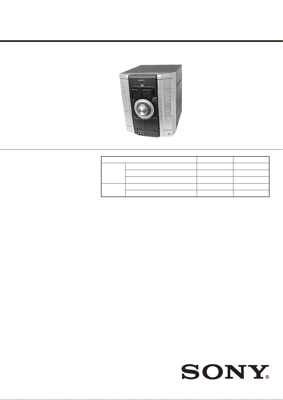
HCD-GX450
SERVICE MANUAL
Ver. 1.2 2005.08
• HCD-GX450 is the tuner, deck, CD and
amplifier section in MHC-GX450.
CD
Section
Tape deck Model Name Using Similar Mechanism New New
Section T ape Transport Mechanism T ype CWM43FF-05 CWM43FF-05
Model Name Using Similar Mechanism New New
CD Mechanism Type CDM74-F1BD81
Optical Pick-up Name
US Model
Canadian Model
Former Type Models
KSM-215DCP/C2NP KSM-213DCP/C2NP
New Type Models
CDM74KF-K6BD81C
Amplifier section
AUDIO POWER SPECIFICATIONS
POWER OUTPUT AND TOTAL HARMONIC
DISTORTION:
With 6 ohm loads, both channels driven, from
120 – 10,000 Hz: rat ed 125 watts per ch annel
minimum RMS power, with no more than 10%
total harmonic distortion from 250 milliwatts to
rated output.
Front speaker
Continuous RMS power output (reference):
125 + 125 watts (6 ohms at
1 kHz, 10% THD)
Total harmonic distortion less than 0.07% (6 ohms at
1kHz, 60 W)
Sub woofer
Continuous RMS power output (reference):
150 watts (6 ohms at
50 Hz, 10% THD)
Total harmonic distortion less than 0.07% (6 ohms at
50 Hz, 75 W)
CD player section
System Compact disc and dig ital
audio system
SPECIFICATIONS
Laser Semiconductor laser
(λ=780 nm)
Emission duration:
continuous
Frequency response 2 Hz – 20 kHz (±0.5 dB)
Wavelength 780 – 790 nm
Signal-to-noise ratio More than 90 dB
Dynamic range More than 90 dB
Tape deck section
Recording system 4-track 2-channel, stereo
Frequency response 50 – 13,000 Hz (±3 dB),
using Sony TYPE I
cassettes
Tuner section
FM stereo, FM/AM super he te rodyne tuner
FM tuner section
Tuning range 87.5 – 108.0 MHz
(100-kHz step)
Antenna FM lead antenna
Antenna terminals 75 ohms unbalanced
Intermediate frequency 10.7 MHz
AM tuner section
Tuning range 530 – 1,710 kHz
(with the tuning interv al
set at 10 kHz)
531 – 1,710 kHz
(with the tuning interv al
set at 9 kHz)
Antenna AM loop antenna
Antenna terminals External antenna terminal
Intermediate frequency 450 kHz
General
Power requirements 120 V AC, 60 Hz
Power consumption
USA models: 265 watts
Canadian models: 330 VA
Dimensions (w/h/d) incl. projecting parts and controls
Amplifier/Tuner/Tape/CD section:
Approx. 280 × 327 ×
425 mm
Mass Approx. 10.0 kg
Design and specifications are subject to change
without notice.
9-877-534-03
2005H16-1
© 2005.08
MINI HI-FI COMPONENT SYSTEM
Sony Corporation
Personal Audio Group
Published by Sony Engineering Corporation
HCD-GX450
SAFETY CHECK-OUT
After correcting the original service problem, perform the
following safety checks before releasing the set to the customer:
Check the antenna terminals, metal trim, “metallized” knobs, screws,
and all other exposed metal parts for AC leakage. Check leakage as
described below.
LEAKAGE
The AC leakage from any exposed metal part to earth ground
and from all exposed metal parts to any exposed metal part having
a return to chassis, must not exceed 0.5 mA (500 microamperes).
Leakage current can be measured by any one of three methods.
1. A commercial leakage tester, such as the Simpson 229 or RCA
WT -540A. Follo w the manufacturers’ instructions to use these
instruments.
2. A battery-operated AC milliammeter. The Data Precision 245
digital multimeter is suitable for this job.
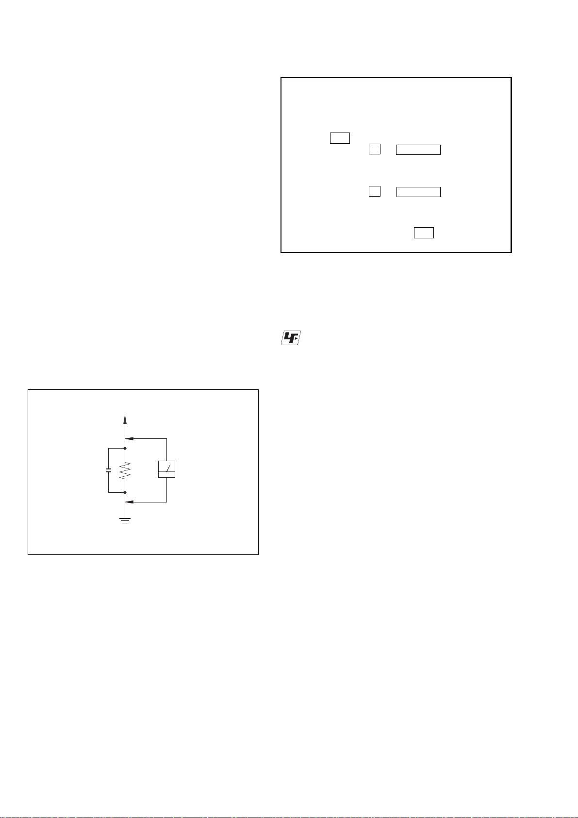
3. Measuring the voltage drop across a resistor by means of a
VOM or battery-operated AC v oltmeter. The “limit” indication
is 0.75 V, so analog meters must have an accurate low-voltage
scale. The Simpson 250 and Sanwa SH-63Trd are e xamples of
a passive VOM that is suitable. Nearly all battery operated
digital multimeters that have a 2V AC range are suitable. (See
Fig. A)
To Exposed Metal
Parts on Set
AC
0.15 µF
1.5 kΩ
Earth Ground
Voltmeter
(0.75 V)
The release method of a CD disc tray LOCK function
There is a disc lock function for the disc theft prevention for a
demonstration at a shop front in this machine.
Procedue:
1. Press the ?/1 button to turn the set on.
2. Press two buttons of x and Z (EJECT) simultaneously for
five seconds.
3. The message “LOCKED” is displayed and the tray is locked.
(Even if exiting from this mode, the tray is still locked.)
4. Press two buttons of x and Z (EJECT) simultaneously for
five seconds again.
5. The message “UNLOCKED” is displayed and the tray is
unlocked.
6. To exit from this mode, press the ?/1 button to turn the set
off.
Unleaded solder
Boards requiring use of unleaded solder are printed with the leadfree mark (LF) indicating the solder contains no lead.
(Caution: Some printed circuit boards may not come printed with
the lead free mark due to their particular size.)
: LEAD FREE MARK
Unleaded solder has the following characteristics.
• Unleaded solder melts at a temperature about 40°C higher than
ordinary solder.
Ordinary soldering irons can be used but the iron tip has to be
applied to the solder joint for a slightly longer time.
Soldering irons using a temperature regulator should be set to
about 350°C.
Caution: The printed pattern (copper foil) may peel away if the
heated tip is applied for too long, so be careful!
• Strong viscosity
Unleaded solder is more viscous (sticky , less prone to flow) than
ordinary solder so use caution not to let solder bridges occur such
as on IC pins, etc.
• Usable with ordinary solder
It is best to use only unleaded solder but unleaded solder may
also be added to ordinary solder.
Fig. A. Using an A C v oltmeter to check A C leakage.
SAFETY-RELATED COMPONENT WARNING!!
COMPONENTS IDENTIFIED BY MARK 0 OR DOTTED LINE WITH
MARK 0 ON THE SCHEMATIC DIAGRAMS AND IN THE PARTS
LIST ARE CRITICAL TO SAFE OPERATION. REPLACE THESE
COMPONENTS WITH SONY PARTS WHOSE PART NUMBERS
APPEAR AS SHOWN IN THIS MANUAL OR IN SUPPLEMENTS
PUBLISHED BY SONY .
ATTENTION AU COMPOSANT AYANT RAPPORT
LES COMPOSANTS IDENTIFÉS P AR UNE MARQUE 0 SUR LES
DIAGRAMMES SCHÉMA TIQUES ET LA LISTE DES PIÈCES SONT
CRITIQUES POUR LA SÉCURITÉ DE FONCTIONNEMENT. NE
REMPLACER CES COMPOSANTS QUE PAR DES PIÈSES SONY
DONT LES NUMÉROS SONT DONNÉS DANS CE MANUEL OU
DANS LES SUPPÉMENTS PUBLIÉS PAR SONY.
À LA SÉCURITÉ!
2
HCD-GX450
NOTES ON HANDLING THE OPTICAL PICK-UP
BLOCK OR BASE UNIT
The laser diode in the optical pick-up block may suffer electrostatic
break-down because of the potential difference generated by the
charged electrostatic load, etc. on clothing and the human body.
During repair, pay attention to electrostatic break-down and also
use the procedure in the printed matter which is included in the
repair parts.
The flexible board is easily damaged and should be handled with
care.
NOTES ON LASER DIODE EMISSION CHECK
The laser beam on this model is concentrated so as to be focused on
the disc reflective surface by the objective lens in the optical pickup block. Therefore, when checking the laser diode emission,
observe from more than 30 cm away from the objective lens.
Laser component in this product is capable
of emitting radiation exceeding the limit for
Class 1.
TABLE OF CONTENTS
1. SERVICING NOTE·························································· 4
2. GENERAL ·········································································· 6
3. DISASSEMBLY
3-1. Cover (Top) ····································································· 9
3-2. CD Door·········································································· 9
3-3. Front Panel Section ······················································· 10
3-4. CD Mechanism Deck (CDM74-F1BD81) ···················· 10
3-5. Tape Mechanism Deck, Game Jack Board ··················· 11
3-6. PANEL Board ······························································· 11
3-7. Back Panel Section, SUB-TRANS Board ···················· 12
3-8. Power Transformer······················································· 12
3-9. MAIN Board ································································· 13
3-10. SUB-WOOFER Board················································ 13
3-11. AMP Board ································································· 14
3-12. BD81A Board ····························································· 14
3-13. CONNECT Board·······················································15
3-14. DRIVER Board, SW Board ········································ 15
3-15. Optical Pick-up (KSM-215DCP/C2NP) ····················· 16
3-16. SENSOR Board ·························································· 16
3-17. MOTOR (TB) Board··················································· 17
3-18. MOTOR (LD) Board ·················································· 17
4. TEST MODE ···································································· 18
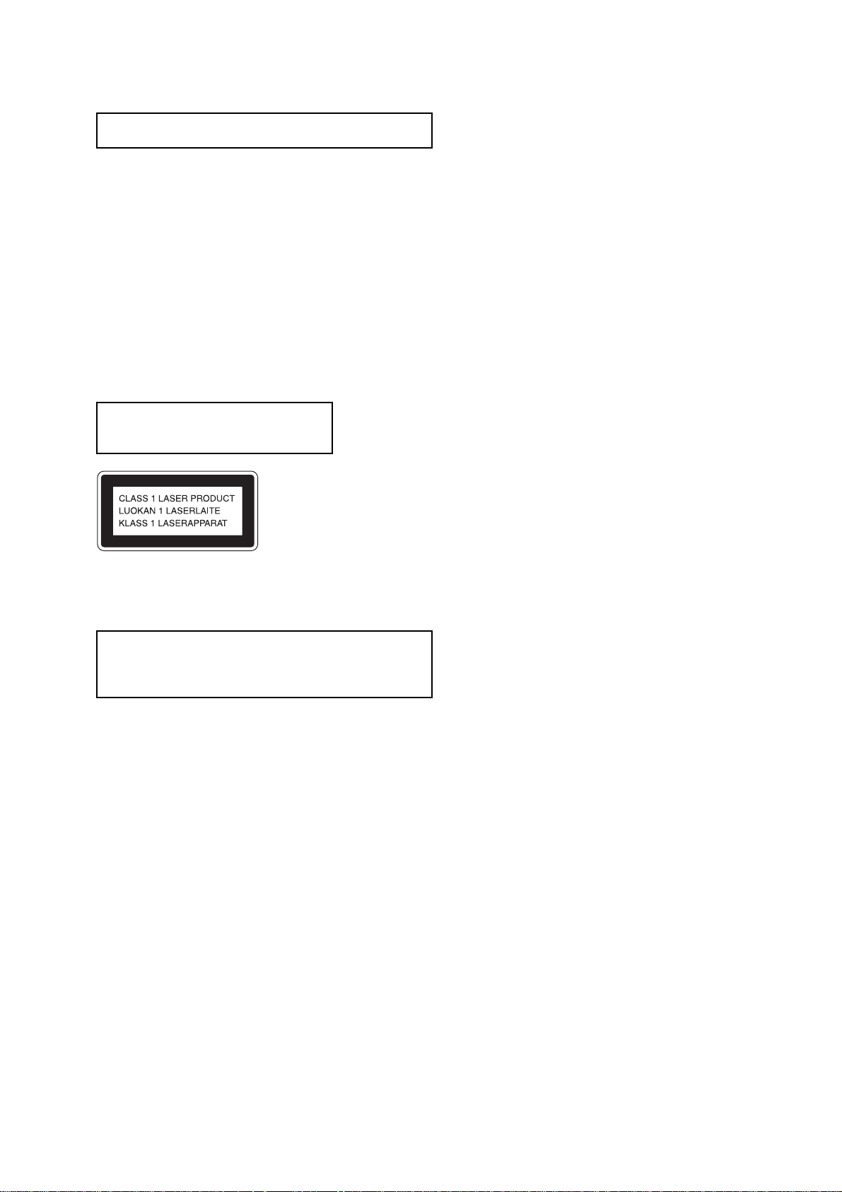
This appliance is classified as a CLASS 1 LASER product. The
CLASS 1 LASER PRODUCT MARKING is located on the rear
exterior.
CAUTION
Use of controls or adjustments or performance of procedures
other than those specified herein may result in hazardous radiation
exposure.
Notes on chip component replacement
•Never reuse a disconnected chip component.
• Notice that the minus side of a tantalum capacitor may be
damaged by heat.
Flexible Circuit Board Repairing
•Keep the temperature of soldering iron around 270˚C
during repairing.
• Do not touch the soldering iron on the same conductor of the
circuit board (within 3 times).
• Be careful not to apply force on the conductor when soldering
or unsoldering.
5. DIAGRAMS
5-1. Block Diagrams – PANEL Section – ···························· 22
– MAIN Section – ······················································· 23
– BD/DRIVER Section – ············································ 24
– SUB-WOOFER Section – ········································ 25
5-2. Printed Wiring Board – BD81A Section –··················· 26
5-3. Schematic Diagram – BD81A Section – ····················· 27
5-4. Printed Wiring Board
– CD MECHANISM Section – ··································· 28
5-5. Schematic Diagram – CD MECHANISM Section –···29
5-6. Printed Wiring Board – MAIN Section – ···················· 30
5-7. Schematic Diagram – MAIN Section (1/2) – ·············· 31
5-8. Schematic Diagram – MAIN Section (2/2) – ·············· 32
5-9. Printed Wiring Board – PANEL COMB Section – ······ 33
5-10. Schematic Diagram – PANEL COMB Section – ······ 34
5-11. Printed Wiring Board – SUB-WOOFER Section – ··· 35
5-12. Schematic Diagram
– SUB-WOOFER Section – ········································ 36
5-13. Printed Wiring Board – PANEL Section –················· 37
5-14. Schematic Diagram – PANEL Section (1/2) – ·········· 38
5-15. Schematic Diagram – PANEL Section (2/2) – ·········· 39
5-16. Printed Wiring Board – TRANS Section – ················ 40
5-17. Printed Wiring Board – AMP Section – ····················· 41
5-18. Schematic Diagram – AMP POWER Section – ········ 42
5-19. IC Pin Function Description ······································· 46
6. EXPLODED VIEWS
6-1. MAIN Section·······························································51
6-2. Front Panel Section ······················································· 52
6-3. MAIN Board Section ···················································· 53
6-4. CD Mechanism Deck Section -1 (CDM74-F1BD81)··· 54
6-5. CD Mechanism Deck Section -2 (CDM74-F1BD81)··· 55
7. ELECTRICAL PARTS LIST ······································· 56
3
HCD-GX450
d
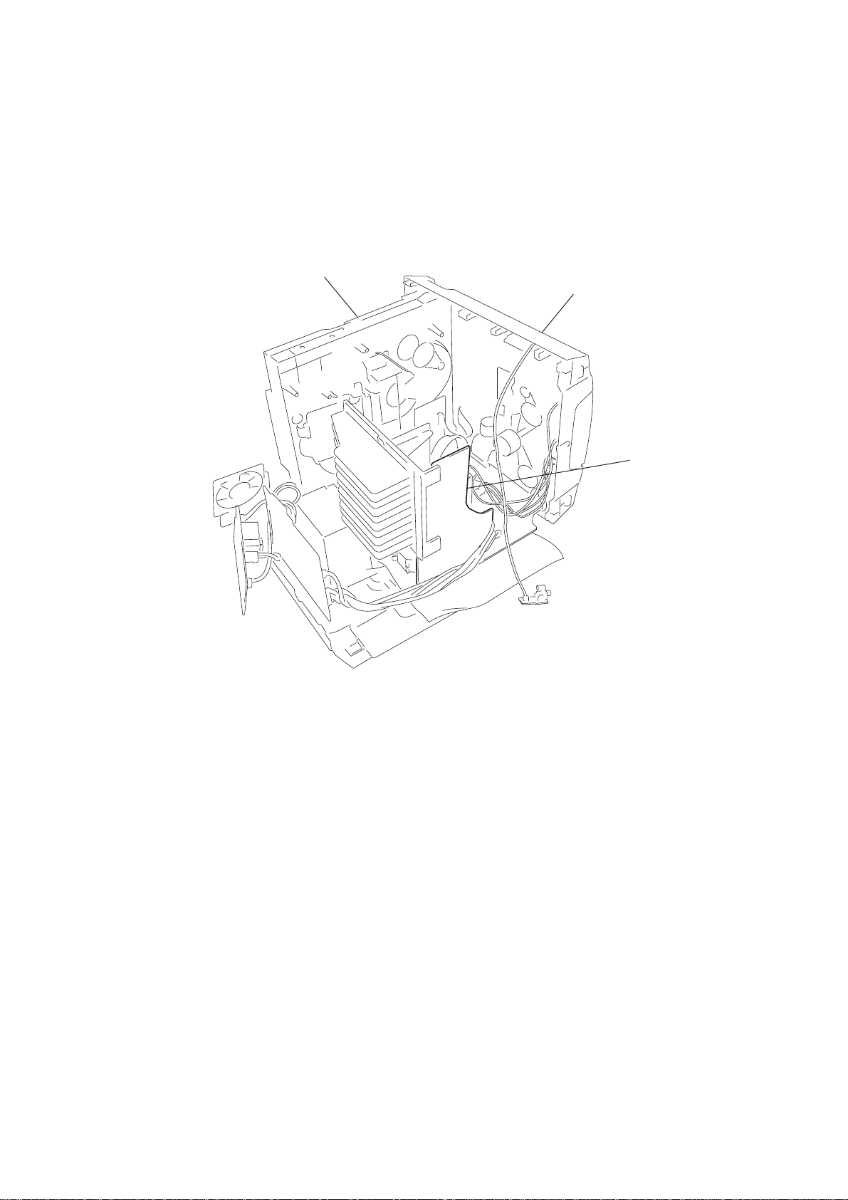
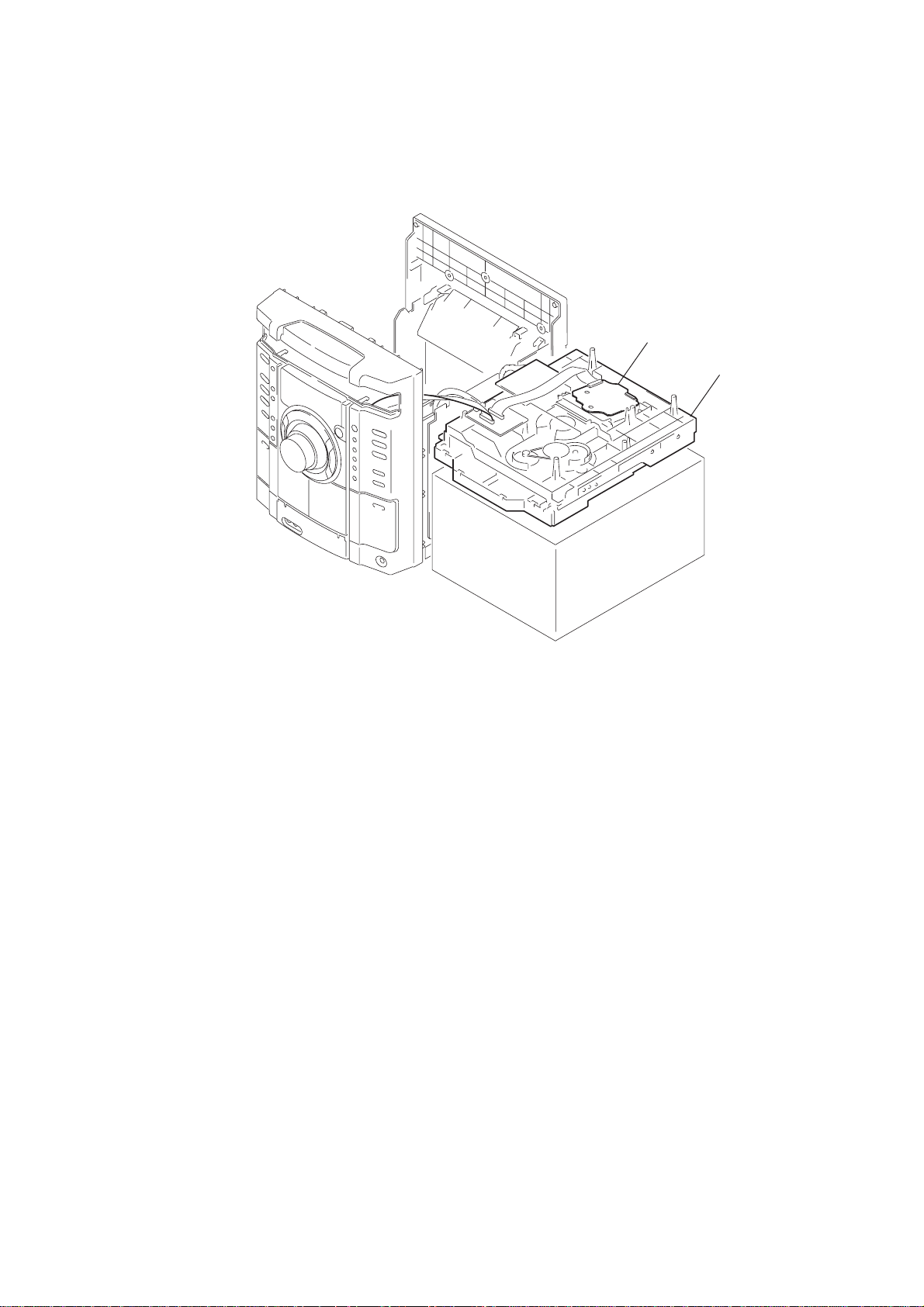
• SERVICE POSITION -1 (AMP BOARD)
To inspect the AMP board, turn both of the front panel
and the CD mechanism deck so that the left side of the product faces down.
CD mechanism deck
SECTION 1
SERVICING NOTE
front panel
AMP boar
4
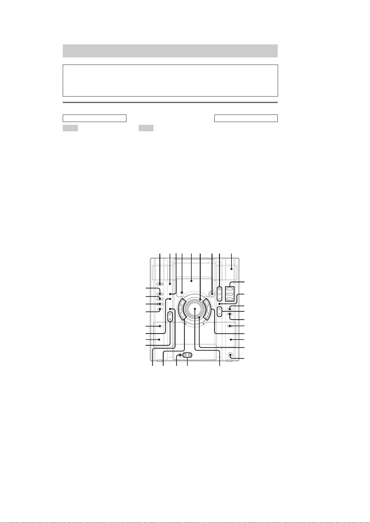
• SERVICE POSITION -2 (BD81A BOARD)
k
Remove the CD mechanism deck and place it on top of the pedestal as shown.
Inspect the BD81A bard in this set up.
HCD-GX450
BD81A board
CD mechanism dec
5
HCD-GX450
Illustrati
SECTION 2
GENERAL
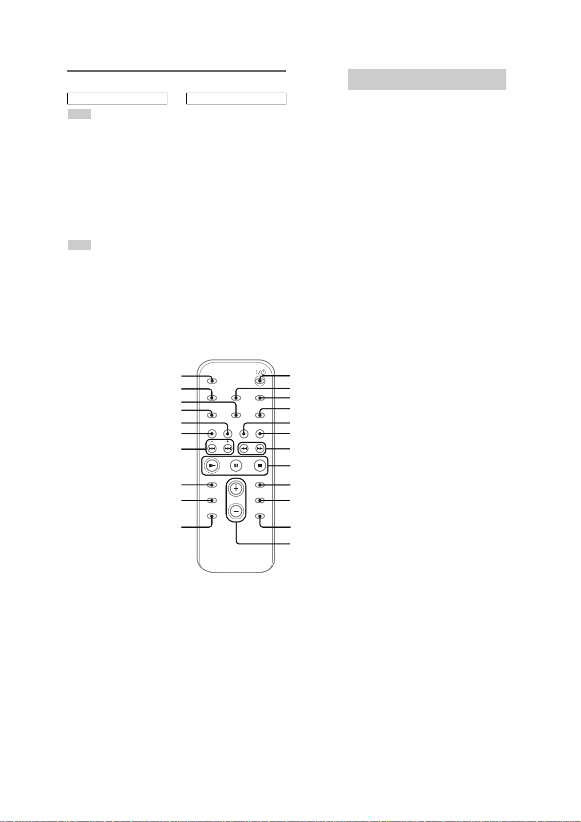
List of button locations and reference pages
How to use this page
Use this page to find the loca tio n of buttons and other
parts of the system that are mentioned in the text.
Main unit
ALPHABETICAL ORDER
A – O P – Z
ALBUM +
ALBUM –
CD eg (9, 11, 14, 19, 20)
CD SYNC wj (19)
Deck A wk (18)
Deck B qj (18, 19, 20, 24)
DISC 1 – 3 q; (12, 14, 35)
DISC SKIP/EX-CHANGE qs
Disc tray 9 (11)
DISPLAY 2 (17, 27, 28)
Display window 5
EFFECT ON/OFF 8 (22)
ENTER qa (14, 15 , 22)
EQ BAND 7 (22)
GAME es (20, 23, 30)
GAME INPUT AUDIO L/R jacks
GAME INPUT VIDEO jack wf
GAME MIXING wh (23)
GROOVE 8 (21)
ILLUMINATION
Operation Dial
qh (12, 14, 19)
wg (12, 14, 19)
(11, 12, 14, 19)
wd (20, 29)
(29)
3 (28)
(– EQ +/l L) 6 (12,
14, 19, 22)
P FILE qd (22)
PHONES jack ql
PLAY MODE wl (12, 14, 18, 19,
20, 35)
Power illuminator qk (28)
PRESET EQ qd (22)
REC PAUSE/START wj (19, 20,
23, 24)
Remote sensor 4
SURROUND 8 (23)
TAPE A/B ed (18, 19, 20, 24)
TUNER/BAND ef (15, 16, 20)
TUNING MODE wl (15, 16, 35)
TUNING + qh (15, 16)
TUNING – wg (15, 16)
VOLUME control w; (21)
12345 6 78 9
eg
ef
ed
es
e;
wl
wk
wj
on number
r
TAPE A/B ed (18, 19, 20, 24)
Name of button/pa rt Reference page
RR
BUTTON DESCRIPTIONS
?/1 (power) 1 (8, 16, 27, 30, 33,
35)
X (pause) wg (12, 19)
Z (eject) qf (11)
PUSH Z (deck B) (eject) qg (18)
x (stop) wg (12, 19, 24, 35)
M (fast forward) qh (12, 19)
H (play) qh (12, 18, 19)
m (rewind) wg (12, 19)
Z PUSH (deck A) (eject) e; (18)
q;
qa
j
ALBUM
S
s
TUNING TUNING
J
ALBUM
H
h
qs
qd
qf
qg
qh
qj
qk
ql
6
wh
wfwg
wd
w;
HCD-GX450
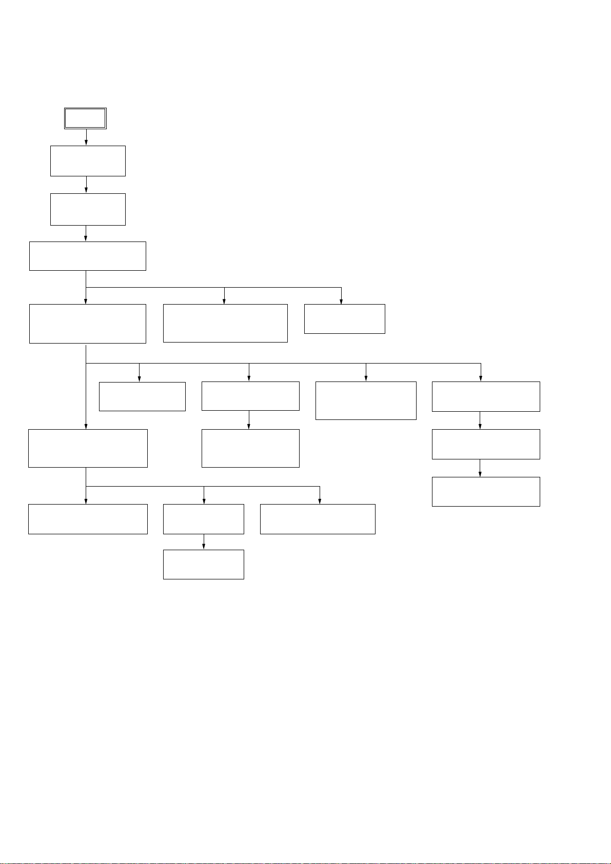
Remote control
ALPHABETICAL ORDER
A – E
ALBUM – qd (12, 14)
ALBUM + qa (12, 14)
CD qk (11, 14)
CLEAR qg (14)
CLOCK/TIMER SELECT 2
(26, 27)
CLOCK/TIMER SET 3 (10, 25,
26)
DISC SKIP q; (12, 14)
DISPLAY wa (17, 27, 28)
ENTER 9 (10, 14, 15, 25, 26)
EQ qf (22)
F – Z
FM MODE 4 (17)
FUNCTION 6 (11, 14, 15, 16)
PLAY MODE w; (12, 14, 18)
REPEAT 4 (13)
SLEEP ws (25)
TAPE qj
TUNER BAND 5 (15, 16)
TUNER MEMORY ql (15)
TUNING MODE w; (15, 16)
VOLUME +/– qs (21, 25)
BUTTON DESCRIPTIONS
?/1 (power) 1 (8, 26)
m/M (rewind/fast forward)
7 (12, 19)
–/+ (tuning) qh (15)
./> (go back/go forward)
qh (10, 12, 19)
N (play) 8 (12, 18)
X (pause) 8 (12, 19)
x (stop) 8 (12, 19)
Setting the clock
Use buttons on the remote for the operation.
1
Press ?/1 to turn on the system.
2
Press CLOCK/TIMER SET.
3
Press . or > repeatedly to set the
hour.
4
Press ENTER.
5
Press . or > repeatedly to set the
minute.
6
Press ENTER.
The clock starts working.
To adjust the clock
1
Press CLOCK/TIMER SE T.
2
Press . or > repeatedly to select
“CLOCK SET”, then press ENTER.
3
Do the same procedures as step 3 to 6
above.
Notes
The clock settings are canceled when you disconnect
the power cord or if a power failure occurs.
ws
wa
w;
ql
qk
qj
qh
qg
qf
qd
1
2
3
4
5
6
7
8
9
q;
qa
qs
7
HCD-GX450
Note: Disassemble the unit in the order as shown below.
SET
3-1.COVER (TOP)
(Page 9)
3-2.CD DOOR
(Page 9)
SECTION 3
DISASSEMBLY
3-3.FRONT PANEL SECTION
(Page 10)
3-4.CD MECHANISM DECK
(CDM74-F1BD81)
(Page 10)
3-12.BD81A BOARD
(Page 14)
3-7.BACK PANEL SECTION,
SUB-TRANS BOARD
(Page 12)
3-8.POWER TRANSFORMER
(Page 12)
3-5.TAPE MECHANISM DECK,
GAME JACK BOARD
(Page 11)
3-13.CONNECT BOARD
(Page 15)
3-14.DRIVER BOARD,
SW BOARD
(Page 15)
3-9.MAIN BOARD
(Page 13)
3-10.SUB-WOOFER BOARD
3-6.PANEL BOARD
(Page 11)
3-15.OPTICAL PICK-UP
(KSM-215DCP/C2NP)
(Page 16)
(Page 13)
3-16.SENSOR BOARD
(Page 16)
3-17.MOTOR (TB) BOARD
(Page 17)
3-18.MOTOR (LD) BOARD
(Page 17)
3-11.AMP BOARD
(Page 14)
8
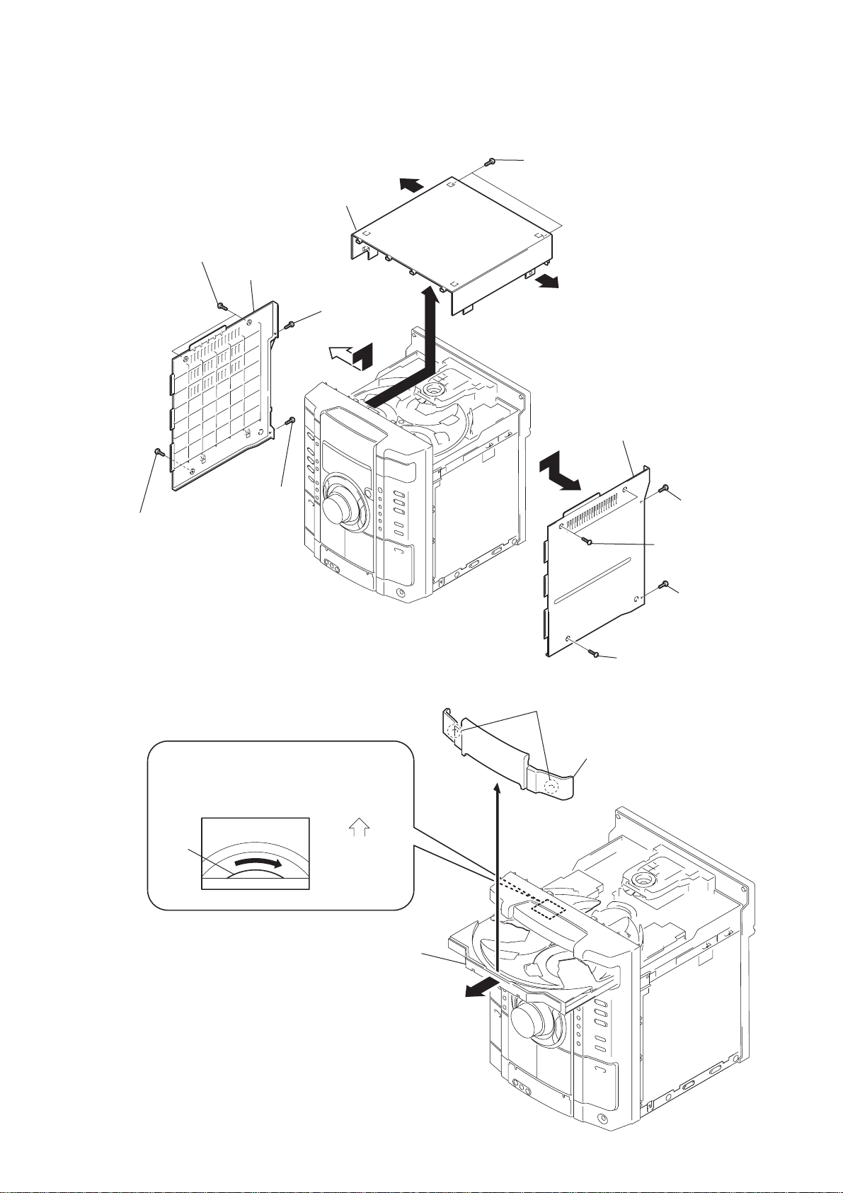
Note: Follow the disassembly procedure in the numerical order given.
3-1. COVER (TOP)
qs
qf
cover
(top)
6
two screws (Case 3 TP2)
cover
(Side-L)
qa
two
screws (+BVTP 3
×
HCD-GX450
10)
7
screw (case 3 TP2)
3-2. CD DOOR
9
screw
(+BVTP 3
× 10
)
8
screw
(+BVTP 3
q;
× 10
qs
)
qd
cover
(Side-R)
5
3
3
two claws
(+BVTP 3
1
two screws
(case 3 TP2)
4
(+BVTP 3
2
screw (Case 3 TP2)
screw
screw
× 10
× 10
)
)
CD mechanism deck (CDM74)
1
Turn the pulley to the direction of arrow.
Front panel side
pulley
2
Pull-out the disc tray.
4
CD door
9
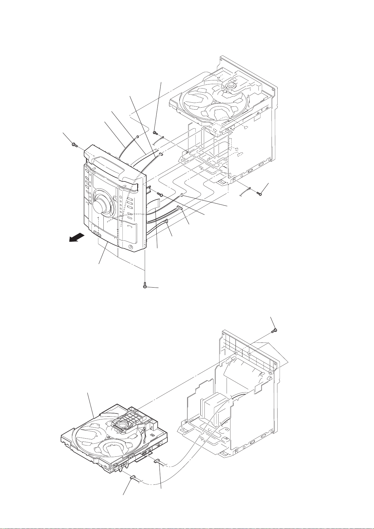
HCD-GX450
)
3-3. FRONT PANEL SECTION
0
connector 3p (CN304C)
8
wire (flat type) 17 core (CN253)
6
connector 2p (CN805)
3
screw (+BVTP 3
×
10)
4
screw (+BVTP 3
× 8
)
5
screw (+BVTP 3
× 8
)
qd
front panel section
3-4. CD MECHANISM DECK (CDM74-F1BD81)
2
screw (+BVTP 3
qs
connector 8p (CN103)
9
connector 5p (CN309)
7
wire (flat type) 29 core (CN302)
1
three screws (+BVTP 3
qa
connector 3p (CN102B)
× 8
)
1
three
×
10)
screws (+BVTP 3
×
10
10
4
CD mechanism deck (CDM74-F1BD81)
3
connector 9p (CN254)
2
connector 12p (CN701)
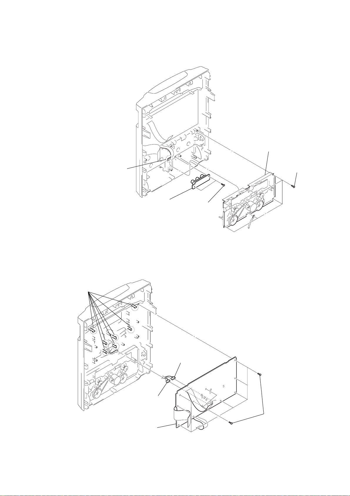
3-5. TAPE MECHANISM DECK, GAME JACK BOARD
)
)
1
wire (flat type) 13 core (CN602)
3
tape mechanism deck
HCD-GX450
2
six
screws
(+BVTP 2.6
×
8
3-6. PANEL BOARD
2
seven
claws
5
GAME JACK board
4
two
(+BVTP 2.6
3
connector 6p (CN604)
screws
×
8)
4
connector 5p (CN605)
5
PANEL board
1
ten
screws
×
(+BVTP 2.6
8
11
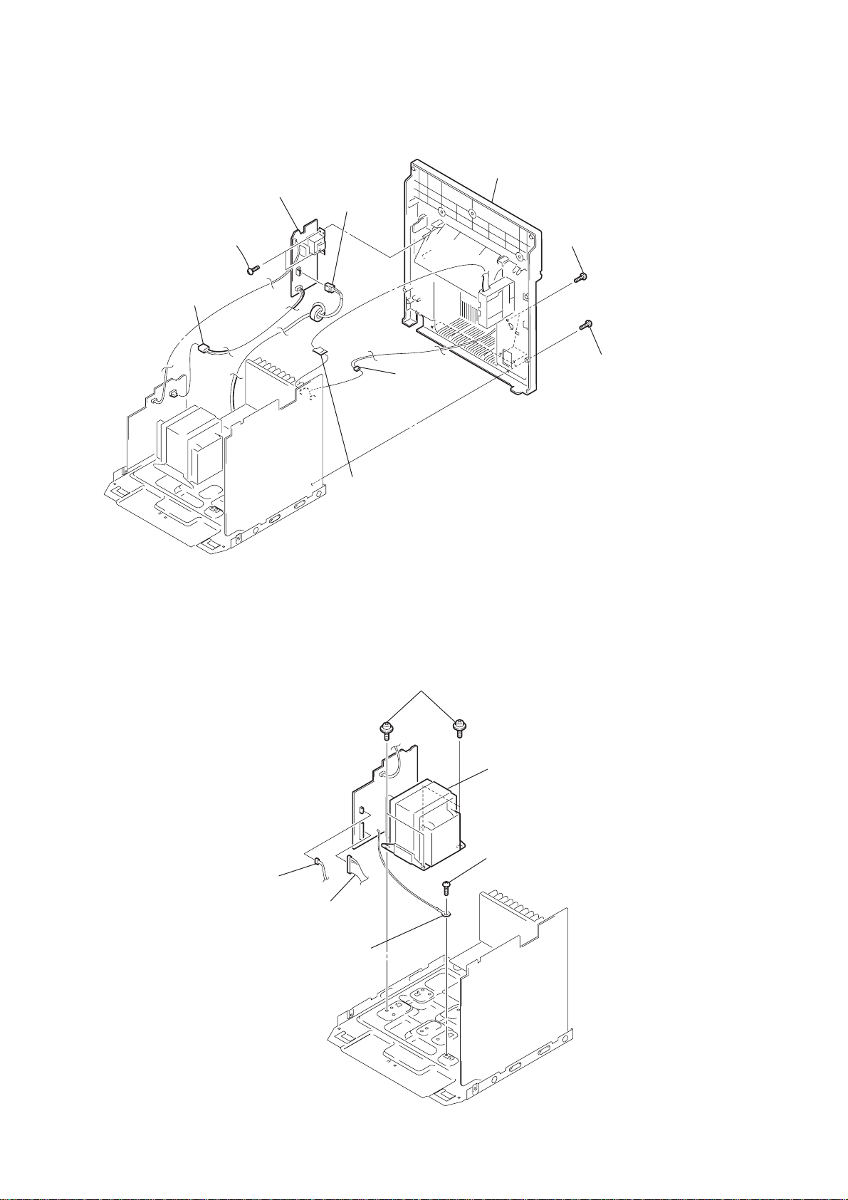
HCD-GX450
)
r
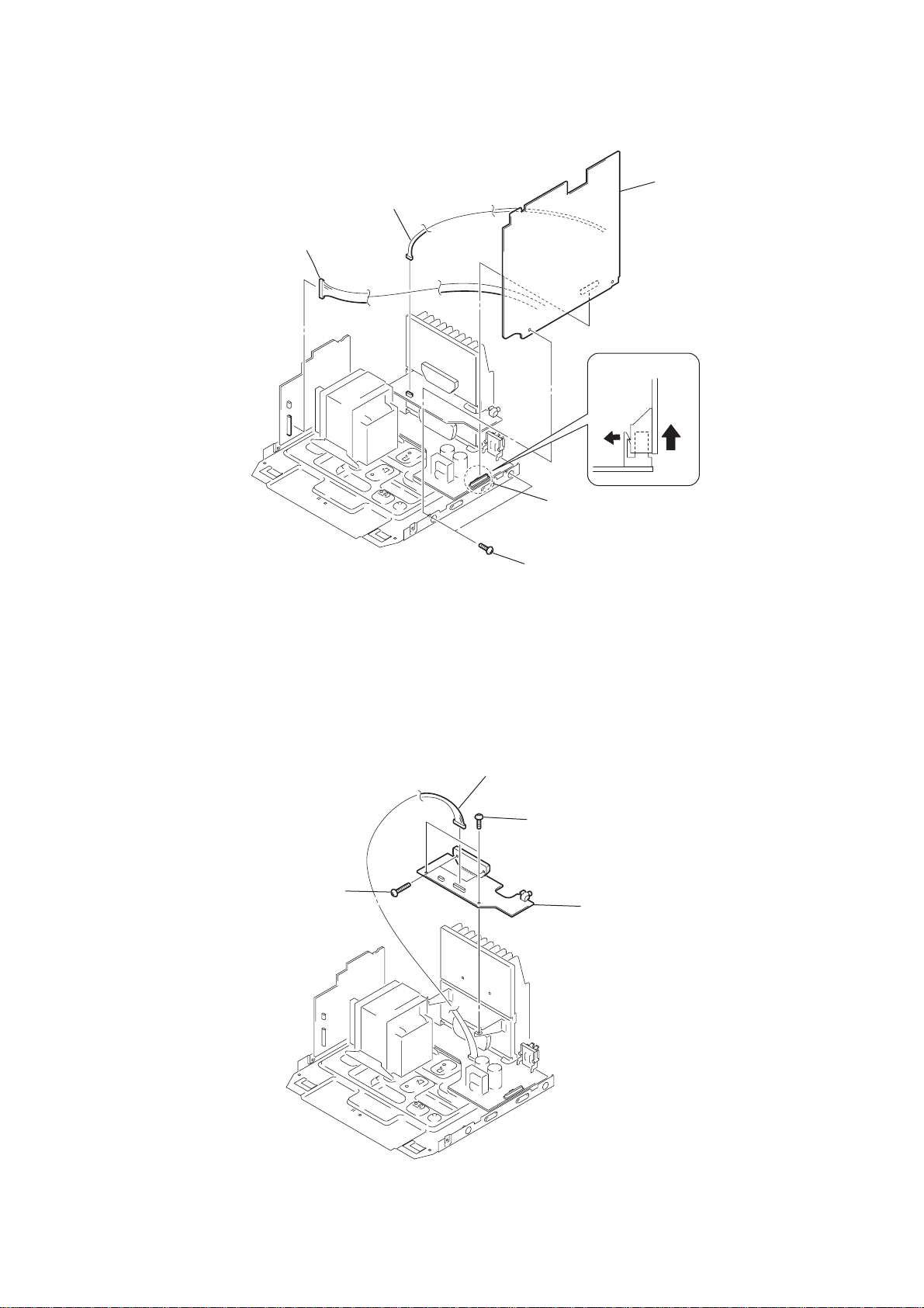
3-7. BACK PANEL SECTION, SUB-TRANS BOARD
7
8
SUB-TRANS board
6
(+BVTT 3
1
connector
2p (CN904)
two
screws
× 10
)
connector
2p (CN901)
3
connector
3p (CN308)
9
back panel section
5
(+BVTT 3
three
screws
×
10)
4
two
screws
(+BVTP 3
×
10
3-8. POWER TRANSFORMER
1
connector
3p (CN905)
2
wire (flat type) 11 core (CN101)
5
four
screws
(+ITC 4
× 8
)
6
power transforme
3
screw
(+BVIT 3
× 8R
)
12
2
connector
10p (CN907)
4
earth wire
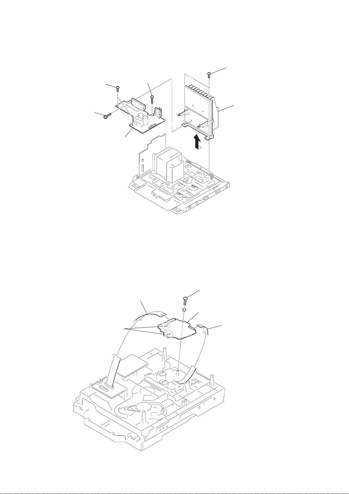
3-9. MAIN BOARD
d
d
1
connector
10p (CN907)
2
connector
4p (CN501)
5
MAIN
Main board
HCD-GX450
boar
3-10. SUB-WOOFER BOARD
2
two
(transistor)
screws
4
13p (CN441)
3
two
(+BVTP 3
1
connector
7p (CN502)
3
two
(+BVTP 3
connector
screws
× 8
)
screws
× 8
)
4
SUB-WOOFER boar
13
HCD-GX450
)
)
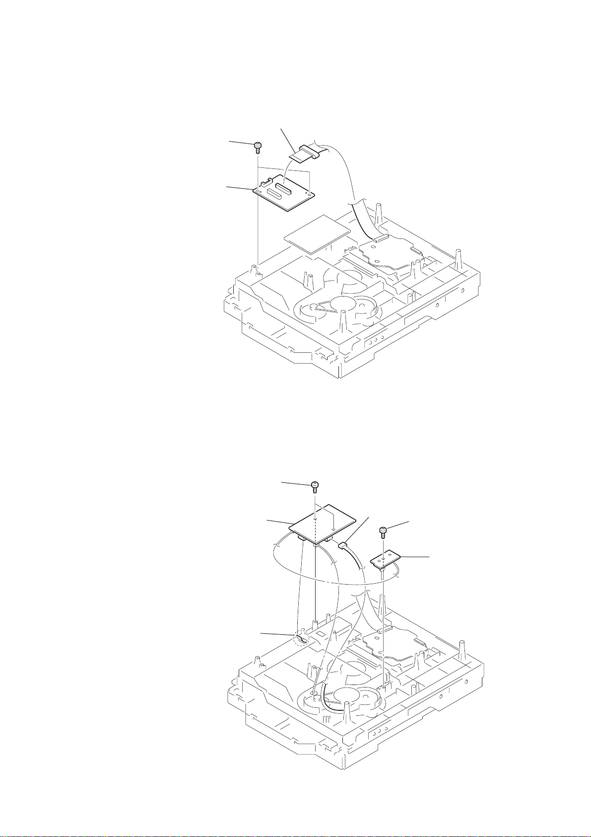
3-11. AMP BOARD
3
two
screws
(+BVIT 3
4
two
screws
(transistor)
× 8R
)
6
AMP
2
screw
(+BVTP 3
board
×
14)
1
two
screws
(+BVTP 3
5
heat sink
× 8
3-12. BD81A BOARD
4
Remove soldering from the four points.
1
wire (flat type) 27 core (CN202)
3
screw
(+BVTP 2.6
5
BD81A
board
× 8
)
2
wire (flat type) 16 core (CN101
14
3-13. CONNECT BOARD
2
two
(+BVTP 2.6
3
CONNECT
screws
board
1
wire (flat type) 27 core (CN251)
× 8
)
HCD-GX450
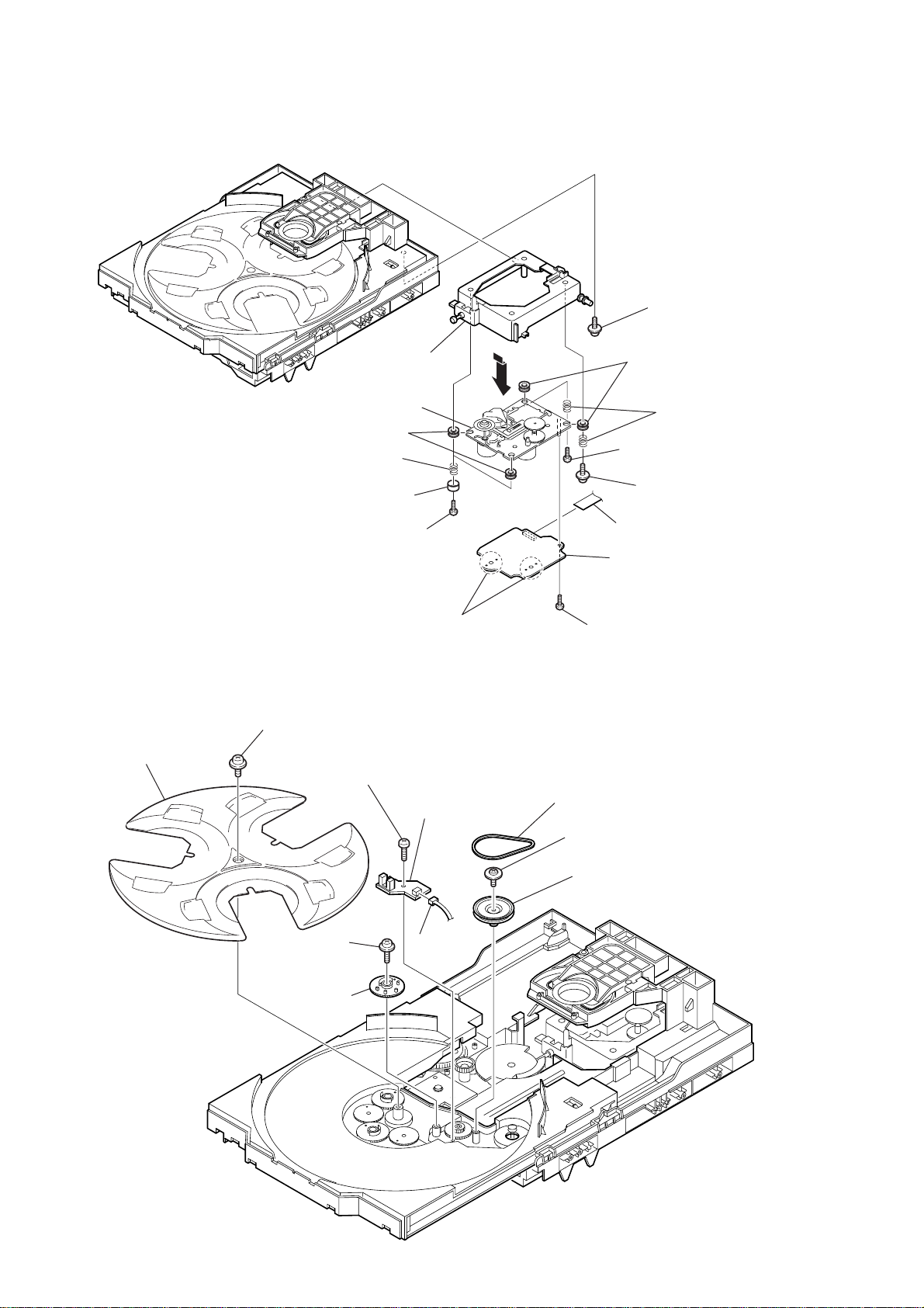
3-14. DRIVER BOARD, SW BOARD
1
(+BTTP (M2.6))
4
DRIVER
2
wire (flat type) 5p (CN702)
two
screws
board
3
connector
4p (CN703)
5
screw
(+BTTP (M2.6))
6
SW board
15
HCD-GX450
3-15. OPTICAL PICK-UP (KSM-215DCP/C2NP)
2
h
qh
optical pick-up
(KSM-215DCP/C2NP)
0
two
insulators
9
two
coil springs
(insulator)
8
t
wo stoppers (BU)
older (213) ASSY
qa
1
floating
(+PTPWH M2.6)
6
two
insulators
5
two
coil springs
(insulator)
3
screw
(BVTT M2.6)
4
floating
(+PTPWH M2.6)
screw
screw
3-16. SENSOR BOARD
2
t
ray
7
(BVTT M2.6)
qd
Remove the four solderings of motor.
1
floating
(+PTPWH M2.6)
6
floating
(+PTPWH M2.6)
screw
8
s
(+BTTP (M2.6))
screw
t
wo screws
crew
0
SENSOR board
9
connector
(
CN731)
qf
CN101 (flat type)
qg
B
D81A board
qs
s
crew (+BVTP 2.6x 8)
3
b
elt (table)
4
floating
(+PTPWH M2.6)
5
screw
p
ulley (table)
16
7
g
ear (geneva)
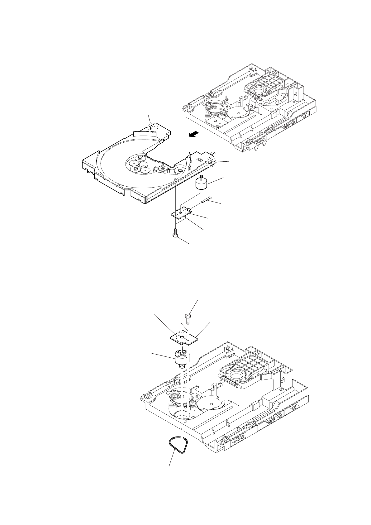
3-17. MOTOR (TB) BOARD
2
stopper
4
1
stopper
5
t
able motor assy (M741)
HCD-GX450
3-18. MOTOR (LD) BOARD
4
Remove the two solderings of motor.
5
l
oading motor assy (M751)
3
7
MOTOR (TB) board
6
Remove the two solderings of motor.
5
two
screws
(+BTTP (M2.6))
2
two
screws
(+BTTP (M2.6))
3
MOTOR (LD) board
wire (flat type) 5 core (CN742)
1
b
elt (loading)
17
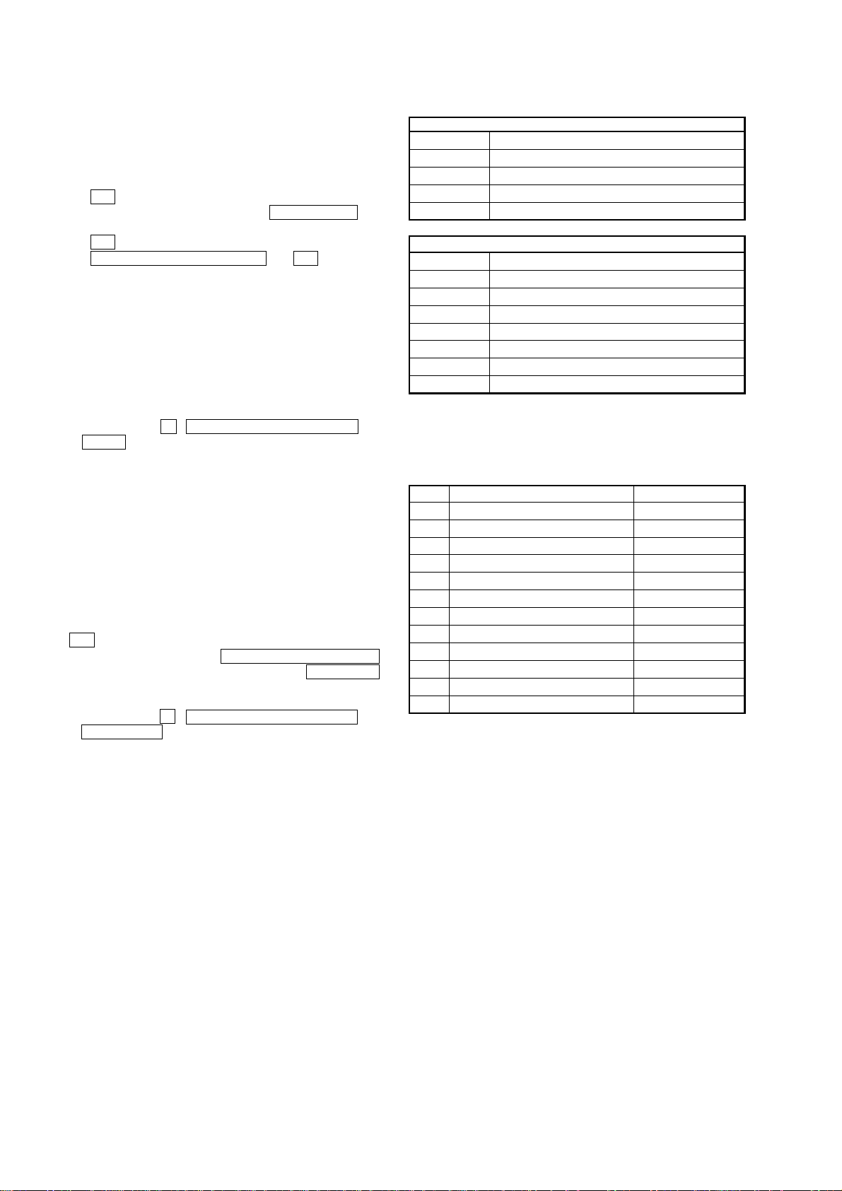
HCD-GX450
SECTION 4
TEST MODE
[Change-over of AM Tuner Step between 9 kHz and
10 kHz]
•A step of AM channels can be changed ov er between 9 kHz and
10 kHz.
Procedure:
1. Press ?/1 button to turn the set ON.
2. Select the function “TUNER”, and press TUNER/BAND
button to select the BAND “AM”.
3. Press ?/1 button to turn the set OFF.
4. Press PLAY MODE/TUNING MODE and ?/1 buttons si-
multaneously, and the display of fluorescent indicator tube
changes to “AM 9 k STEP” or “AM 10 k STEP”, and thus the
channel step is changed over.
[Cold Reset]
• The cold reset clears all data including preset data stored in the
RAM to initial conditions. Execute this mode when returning
the set to the customer.
Procedure:
1. Press three buttons x , PLAY MODE/TUNING MODE ,
and DISC 1 simultaneously.
2. The fluorescent indicator tube displays “COLD RESET” and
the set is reset.
[Aging Mode]
This mode can be used for operation check of CD section and tape
deck section.
• If an error occurred:
The aging operation stops and is displayed status.
• If no error occurs:
The aging operation continues repeatedly.
1. Operating method of Aging Mode
Press ?/1 button to turn the set ON and select “CD” of the function.
1) Set three discs in tray. Press the
PLA Y MODE/TUNING MODE
button to set the “ALL DISCS” mode, and the PRESET EQ
button to “REPEAT” off.
2) Load the tapes recording use into both decks.
3) Press three buttons x , PLAY MODE/TUNING MODE ,
and EX-CHANGE simultaneously.
4) Aging operations of CD and tape are started at the same time.
5) To exit the aging mode, perform [Cold Reset].
2. Aging mode in CD section
1) Operation during aging mode
• In the agining mode ,the program is excuted in the following
sequence.
(1) The disc tray opens and closes.
(2) The disc tray turns to select a disc 3.
(3) The pick-up accesses to the first track, and plays 3 seconds.
(4) The pick-up accesses to the last track, and plays 3 seconds.
(5) The disc tray opens and closes.
(6) The disc tray turns to select a disc 1.
(7) The same operation starts like step (3).
(8) After a disc 1 aging operation, a disc 2 is selected.
(9) When an aging operation of a disc 3 is completed, the display
“AGING ∗∗∗∗” value increases.
(10) If no error occurs, the aging operation continues repeatedly.
2) Error display
Disc error
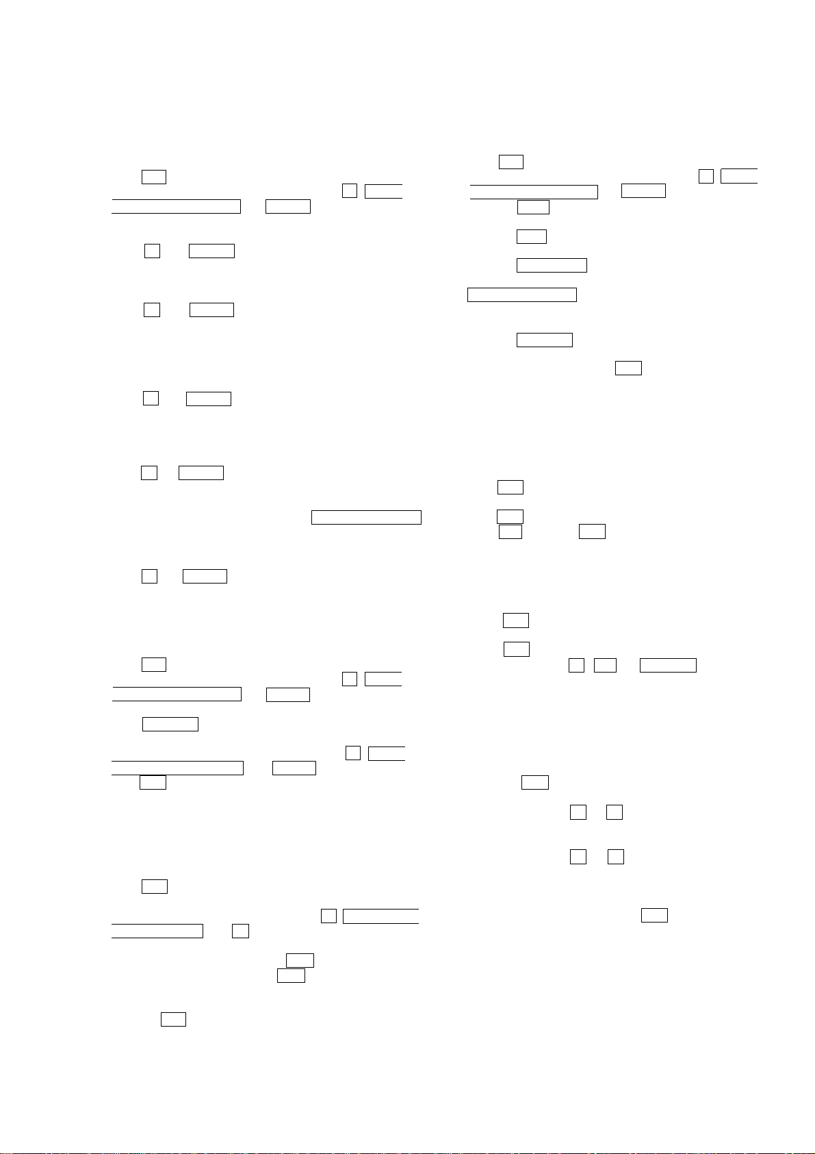
Display Error
E00D01022 Focus error (No disc)
E00D02022 Sub Q error (Focus is good)
E00D02023 TOC reading error
E00D02014 Access error (Unable within regular time)
Mechanism error
Display Error
E00M__E_0 Error during opening tray
E00M__C_2 EX-CHANGE disc error
E00M__D_0 Error during closing tray
E00M__F_3 EX-OPEN error
E00M__D_5 EX-CLOSE error
E00M__C_2 Chuck-up error
E00M__C_3 Unchucking error
3. Aging mode in Tape Deck section
1) Operation during aging mode
• In the agining mode, the program is excuted in the following
sequence.
Step
1
Rewind the TAPE A
2
Rewind the TAPE B
3
Play the TAPE A (1 minute)
4
Stop the TAPE A (1 second)
5
Play the TAPE A (3 minutes)
6
Rewind(AMS) the TAPE A
7
F.F.(AMS) the TAPE A
8
Play the TAPE B (1 minute)
9
Stop the TAPE B (1 second)
10
Record the TAPE B (3 minutes)
11
Rewind(AMS) the TAPE B
12
F.F.(AMS) the TAPE B
Operation
Display
TAPE AAG-1
TAPE BAG-2
TAPE AAG-2
TAPE AAG-3
TAPE AAG-4
TAPE AAG-5
TAPE AAG-6
TAPE BAG-2
TAPE BAG-3
TAPE BAG-4
TAPE BAG-5
TAPE BAG-6
2) Error display
• If error occurred, the display remains like “TAPE BAG-2”.
4. Exiting from the aging mode
• Be sure to perform Cold Reset to exit from the aging mode.
18
HCD-GX450
[P ANEL Test Mode]
• All fluorecent segments and LEDs are tested.
•Keyboard check.
Procedure:
1. Press ?/1 button to turn the set ON.
2. To enter the test mode, press the three buttons x , PLAY
MODE/TUNING MODE and ENTER simultaneously.
3. All segments and LEDs (without STANDBY LED) are turned
on.
4. Press X and ENTER buttons simultaneously, and the key
check mode is activated.
5. The message “KEY 0 0 0 ” is displayed.
Each time a button is pressed, the key code number is displayed.
6. Press X and ENTER buttons simultaneously, and the key
count mode is activated.
7. The message “KEYCNT 0” is displayed.
Each time a button is pressed, “KEYCNT 0” value increased.
However, once a button is pressed, it is no longer taken into
account.
8. Press X and ENTER buttons simultaneously, and the head
phone detect mode is activated.
9. The message “H_P OFF” is displayed when a headphone jack
is not inserted.
“H_P ON ” is displayed when a headphone jack is inserted.
10. Press X and ENTER b uttons simultaneously , and the volume
control detect mode is activated.
11. The message “VOLUME FLAT” is displayed.
“VOLUME UP” is displayed if rotating MASTER VOLUME
knob clockwise, or “VOLUME DO WN” is displayed if rotating
counterclockwise.
12. To exit from the GC test mode after the head phone detect mode,
press X and ENTER buttons simultaneously.
[Version and Destination Display Mode]
•The version or destination is displayed.
Procedure:
1. Press ?/1 button to turn the set ON.
2. To enter the test mode, press the three buttons x , PLAY
MODE/TUNING MODE and DISC 2 simultaneously.
3. The destination is displayed.
4. Press DISPLAY buttons simultaneously.
5. The version is displayed.
6. To exit from this mode, press the three buttons x , PLAY
MODE/TUNING MODE and DISC 2 simultaneously and
press ?/1 button to turn the set OFF.
[CD Service Mode]
•This mode can run the CD sled motor freely. Use this mode, for
instance, when cleaning the pick-up.
Procedure:
1. Press ?/1 button to turn the set ON.
2. Select the function “CD”.
3. To enter the test mode, press three b uttons x , PLAY MODE/
TUNING MODE , and Z simultaneously.
4. The CD service mode is selected.
5. With the CD in stop status, press M button to move the
pick-up to outside track, or press m button to inside track.
6. To exit from this mode, perform as follows:
1) Move the pick-up to the most inside track.
2) Press ?/1 button to turn the set OFF.
Note: • Always move the pick-up to most inside track when exiting from
this mode. Otherwise, a disc will not be unloaded.
• Do not run the sled motor excessively, otherwise the gear can be
chipped.
[MC Test Mode]
•This mode is used to test the function of the equalizer.
Procedure:
1. Press ?/1 button to turn the set ON.
2. To enter the test mode, press the three buttons x , PLAY
MODE/TUNING MODE and DISC 3 simultaneously.
3. Press the EQ + button.
The function of the equalizer is set to “MAX”.
4. Press the EQ - button.
The function of the equalizer is set to “MIN”.
5. Press the PRESET EQ button.
The function of the equalizer is set to “EQ FLAT”.
6. MASTER VOLUME up and down.
“VOLUME MIN” “VOLUME 16” “VOLUME MAX” is
displayed.
7. Press the GROOVE button.
The message “VACS OFF” or “VACS ON” is displayed.
8. To exit from this mode, press ?/1 button to turn the set OFF.
[CD Ship Mode (LOCK) ]
•This mode moves the pick-up to the position durable to vibra-
tion. Use this mode when returning the set to the customer after
repair.
Procedure:
1. Press ?/1 button to turn the set ON.
2. Select the function “CD”.
3. Press ?/1 button to turn the set OFF.
4. Press CD button and ?/1 button simultaneously.
5. The “ST ANDBY” display blinks instantaneously, the message
“LOCK” is displayed and the CD ship mode is set.
[CD Ship (LOCK) & COLD RESET MODE]
Procedure:
1. Press ?/1 button to turn the set ON.
2. Select the function “CD”.
3. Press ?/1 button to turn the set OFF.
4. Press three buttons x , CD and DISPLAY simultaneously.
5. The “ST ANDBY” display blinks instantaneously and CD ship
mode is set.
6. To fluorescent indicator tube displays “COLD RESET” and
the set is reset.
[Disc T ray Lock]
Procedure:
1. Press the ?/1 button to turn the set ON.
2. Select the function “CD”.
3. Press two buttons of x and Z simultaneously for f ive seconds.
4. The message “LOCKED” is displayed and the tray is locked.
(Even if exiting from this mode, the tray is still locked.)
5. Press two buttons of x and Z simultaneously for five seconds
again.
6. The message “UNLOCKED” is displayed and the tray is
unlocked.
7. To exit from this mode, press the ?/1 button to turn the set
OFF.
19

HCD-GX450
[CD Repeat 5 Times Limit Release Mode]
Procedure:
1. Press ?/1 button to turn the set ON.
2. Select the function “CD”.
3. Press three buttons x , CD and ENTER simultaneously.
4. The message “LIMIT OFF” is displayed.
5. Press ?/1 button the set OFF.
[AMP TEST MODE]
Procedure:
1. Press ?/1 button to turn the set ON.
2. To enter the test mode, press three buttons x , PLAY
MODE/TUNING MODE and ENTER simultaneously.
3. Press the DISPLAY button.
The message “V0 0 0” “ 000” is displayed.
4. Press the GROOVE button.
The message “DBFB ON” “DBFB OFF” is displayed.
5. Press the SURROUND button.
The message “SURROUND ON” “SURROUND OFF” is
displayed.
6. Press the EQ BAND button.
The message “LOW” “MID” “HIGH” is displayed.
7. Press ?/1 button to turn the set OFF.
20
SECTION 5
d
DIAGRAMS
THIS NOTE IS COMMON FOR PRINTED WIRING BOARDS AND SCHEMA TIC DIAGRAMS.
(In addition to this, the necessary note is printed in each bloc k.)
Note on Schematic Diagram:
• All capacitors are in µF unless otherwise noted. pF: µµF
50 WV or less are not indicated except for electrolytics
and tantalums.
• All resistors are in Ω and 1/
specified.
f
•
• C : panel designation.
• A : B+ Line.
• B : B– Line.
• H : adjustment for repair.
•Voltages and waveforms are dc with respect to ground
•Voltages are taken with a VOM (Input impedance 10 MΩ).
•Waveforms are taken with a oscilloscope.
• Circled numbers refer to waveforms.
• Signal path.
: internal component.
Note:
The components identified by mark 0 or dotted
line with mark 0 are critical for safety.
Replace only with part
number specified.
under no-signal (detuned) conditions.
Voltage variations may be noted due to normal produc-
tion tolerances.
no mark : FM
( ): CD STOP
Voltage variations may be noted due to normal production tolerances.
F : TUNER
E : PB (DECK A)
d : PB (DECK B)
G : REC (DECK B)
J : CD
f : AUDIO
4
W or less unless otherwise
Note:
Les composants identifiés par
une marque 0 sont critiques
pour la sécurité.
Ne les remplacer que par une
piéce portant le numéro
spécifié.
Note on Printed Wiring Boards:
• X : parts extracted from the component side.
• b : Pattern from the side which enables seeing.
Caution:
Pattern face side: Parts on the pattern face side seen from
(SIDE A) the pattern face are indicated.
Parts face side: Parts on the parts face side seen from
(SIDE B) the parts face are indicated.
• Indication of transistor.
C
These are omitted.
Q
B
CE
These are omitted.
•Abbreviation
CND : Canadian model
Q
B
HCD-GX450
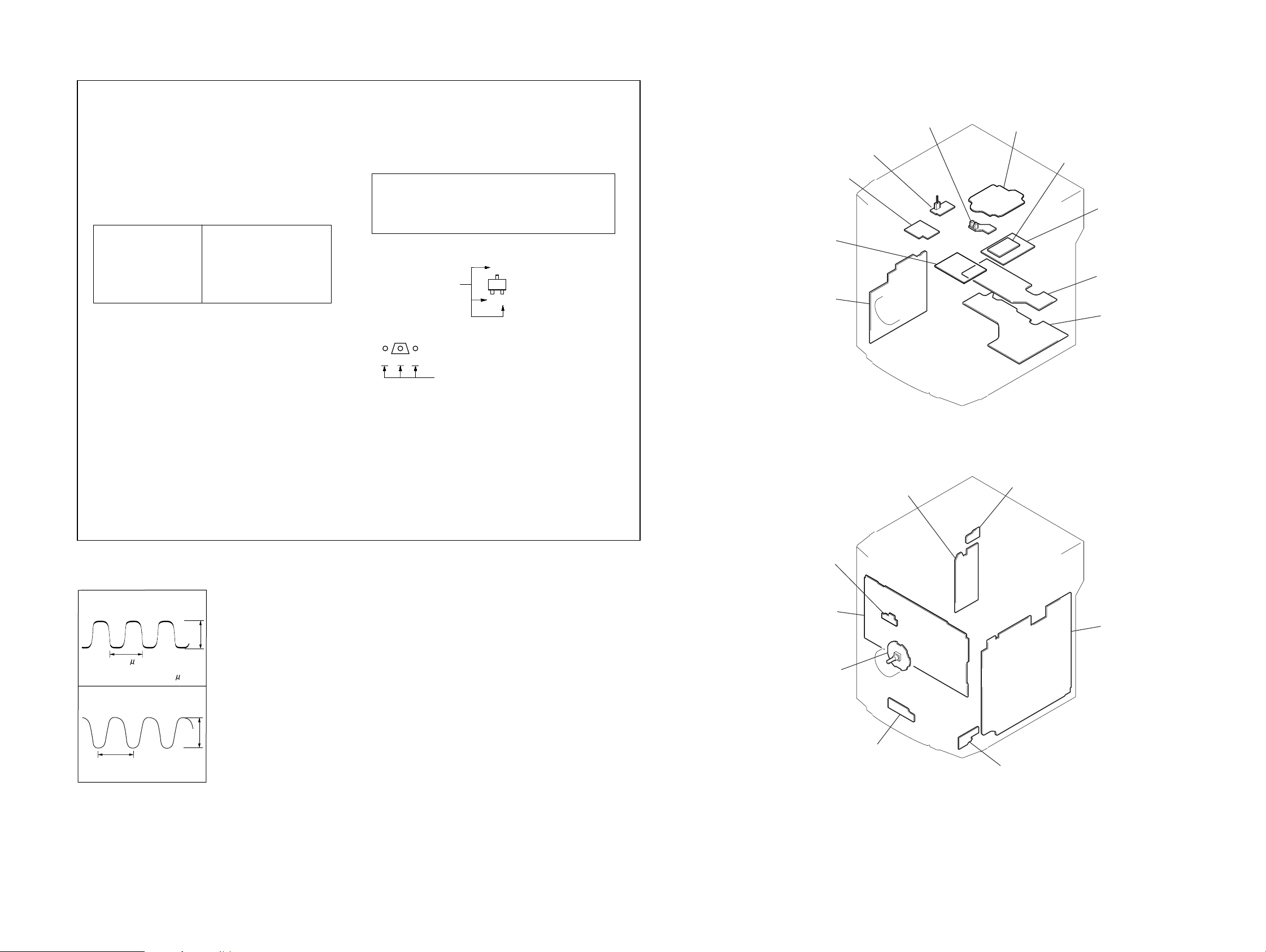
Circuit Boards Location
SENSOR board
SW board
MOTOR (LD) board
CONNECT board
E
TRANS board
SUB-TRANS board
BD81A board
MOTOR (TB) board
DRIVER board
SUB-WOOFER boar
AMP board
VIDEO OUT board
• Waveforms
– PANEL BOARD –
1 IC601 qd (I-XT2)
30.5 s
2 V/DIV, 10 s/DIV
2 IC601 qh (CF2)
100 ns
2 V/DIV, 40 ns/DIV
5.2 Vp-p
4.9 Vp-p
REM board
PANEL board
MAIN board
6 STREAM LED board
GAME JACK board
H/P JACK board
2121
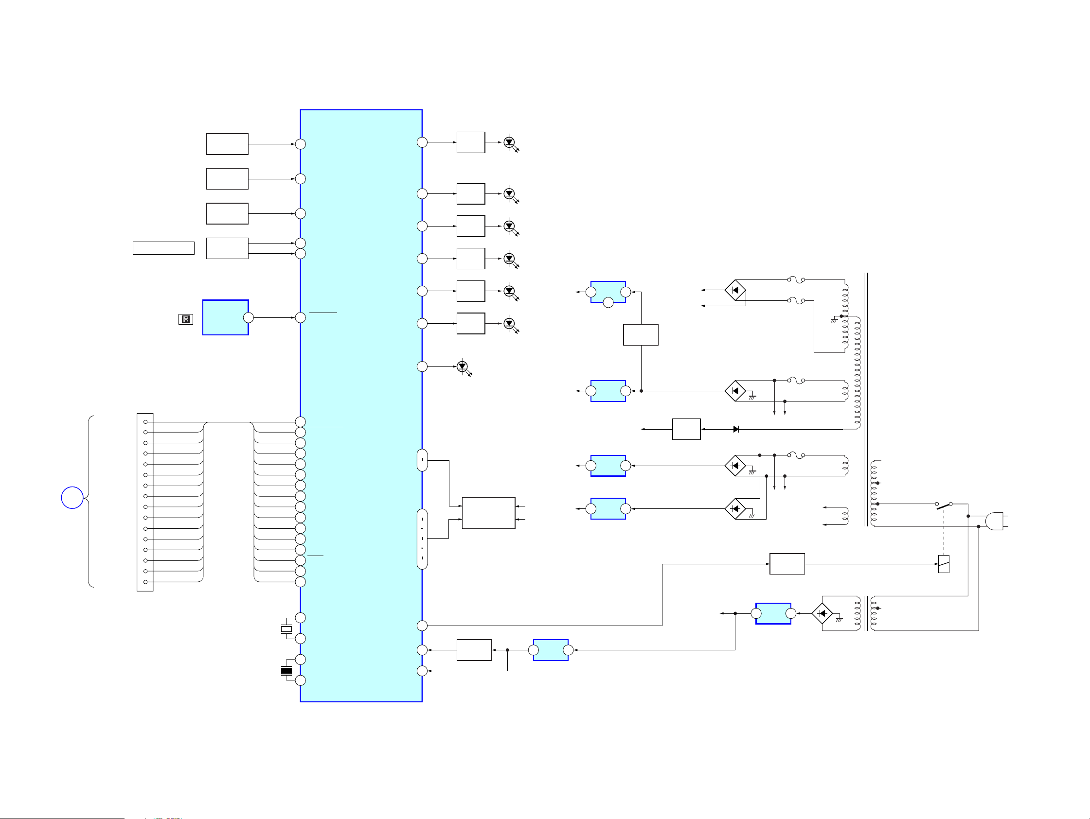
HCD-GX450
5-1. BLOCK DIAGRAMS – PANEL SECTION –
IC601(1/2)
SYSTEM CONTROLLER
BD/DRIVER
SECTION
A
SCOR
XTCN
XRST
XL-T-CD
CD-DATA
SENS
CD-CLK
MP3-DO
MP3-DI
MP3-CLK
MP3-CS
MP3-CP
MP3-ACK
MP3-REQ
MP3-RESET
MP3-STB
MASTER VOLUME
CN603
C1
C2
C3
C4
C5
C6
C7
C8
C9
C10
C11
C12
C13
C14
C15
C18
S641-S650
FUNCTION
KEY
S601-S612
FUNCTION
KEY
S621-S630
FUNCTION
KEY
S851
ENCODER
IC610
REMOTE
CONTROL
RECIEVER
C18
C15
C14
C13
C12
C11
C10
C9
C8
C7
C6
C5
C4
C3
C2
C1
X601
32.768kHz
X602
10MHz
25 KEY3
27 KEY1
26 KEY2
9 VOLUME-IN1
10 VOLUME-IN2
283 SIRDS-IN
MP3-TTB
80
MP3-RESET
6
MP3--REQ
4
MP3-ACK
3
MP3-CS
2
MP3-CS'
1
MP3-CLK
100
MP3-DI
99
MP3-DO
98
CD-CLK
97
SENS
96
CD-DATA
95
XLT
94
XRES
93
XTCN
92
SCOR
5
12 I-XT1
13 I-XT2
15 CF1
16 CF2
G01-G13
S1-S21
POWER RELAY
Q610
82STREM-LED1
80STREM-LED3
81STREM-LED2
77STREM-LED6
78STREM-LED5
79STREM-LED6
76POWER LED
42
30
43
45
47
50
52
65
74
11RESET
29ACCUT
LED
DRIVER
Q612
LED
DRIVER
Q611
LED
DRIVER
Q614
LED
DRIVER
Q615
LED
DRIVER
Q613
LED
DRIVER
LED601
FLUORESCENT
INDICATOR
Q605
RESET
SWITCH
FL601
TUBE
LED610
LED612
LED611
LED615
LED614
LED613
VF
-VFL
IC604
RESET
+3.5V
+3.5V
+9V
+9V
PT901
POWER TRANSFORMER
VF
D902-905
SUB TRANSFORMER
RY901
AC
IN
PT902
AC3
AC4
IC603
REG
F904
F905
F906
F907
RELAY
DRIVE
15
IC302
REG
12
4
Q301,Q302
SWITCH
IC301
REG
13
-VFL
IC303
REG
13
IC304
REG
13
13
+B
-B
Q902
REG
D401
D301-D304
D902
D305-D308
D309-D312
Q361,Q362,Q314,Q315
+3.3V
2222
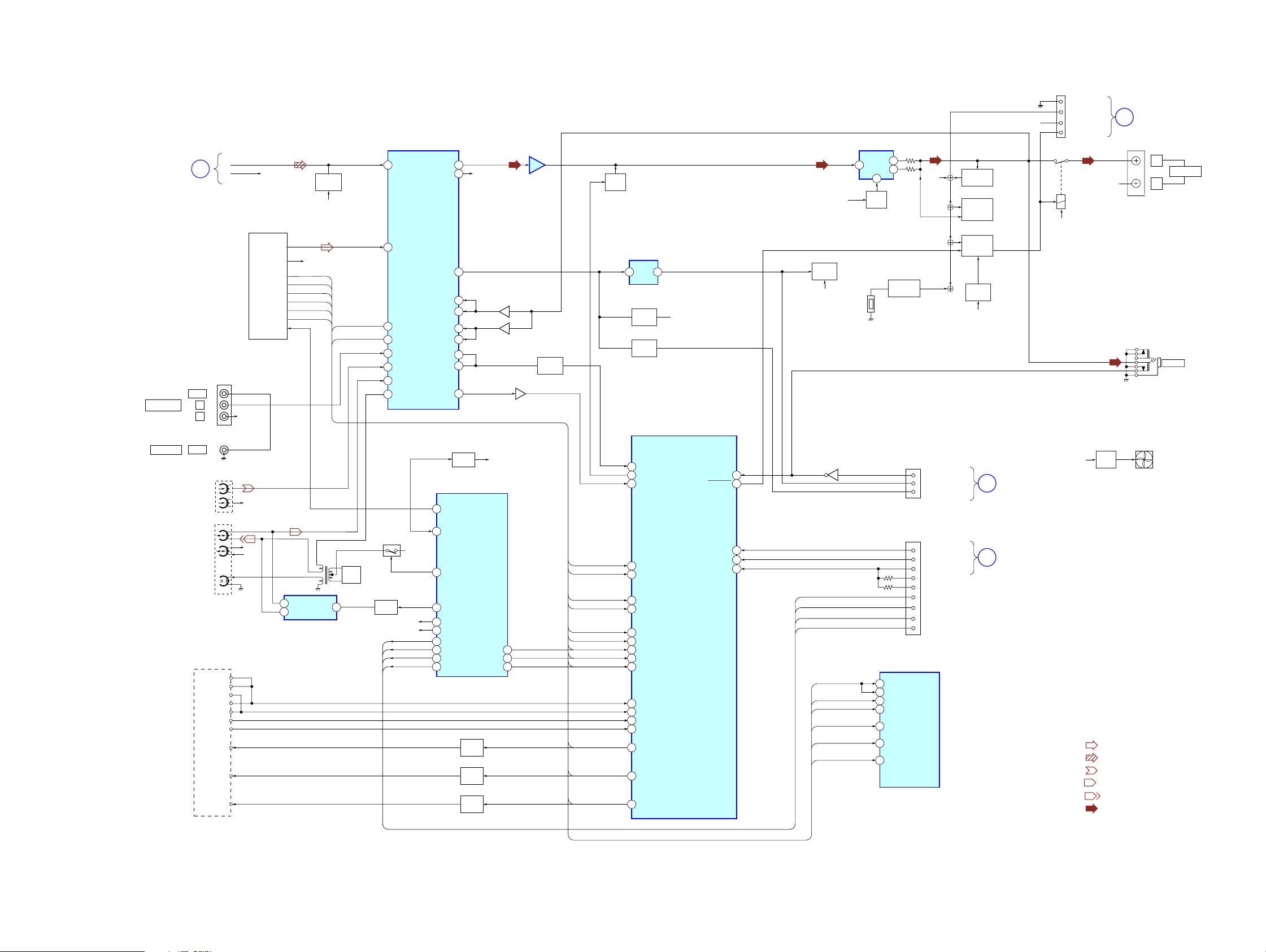
– MAIN SECTION –
BD/DRIVER
SECTION
GAME INPUT
VIDEO OUT
B
J804
VIDEO
L
R
J803
VIDEO
DECK-A
LRHP2
HP1
DECK-B
L
HRP2
R
HRP1
HE1
TAPE
MECHANISM DECK
PWDEWC B
MODE B
MODE A
B HALF
A HALF
A-PHOTO
B-PHOTO
COMP
SOLA
CD-L
CD-R
R-CH
R-CH
R-CH
R-CH
TUNER
TUNER-L
TUNER-R
CLK
TUNED
STEREO
TU-MUTE
DO
DI
CE
Q304-Q307
REC SW
9
P/B SW
7
SELECTOR
IC201
CD-MUTE
R-CH
CLK
TUNED
STEREO
CONT
SWITCH
DO
DI
CE
L101
4
DATA
RCLK
Q321
BIAS
OSC
1 CDL
61 TUNER_L
19 SI
18 SO
59 GAME-L
9 TAPEA1
11 TAPEB1
15 REC-OUT1
Q324
Q322,Q323
SWITCH
IC101
SOUND PROCESSOR
+9V
CD-MUTE
FAN
LM-R
LM-F
TM-R
TM-F
BBNF1
BBIN1
BBNF2
SAOUT2
SAOUT1
11 Q5
12 Q6
7Q1
6Q0
10 Q4
17 Q11
13 Q7
14 Q8
15 Q9
16
32VOUT2
33VOUT1
25 5 1SW OUT
34
35
31BBNF2
30
55
56
40ASMOUT
Q308,Q309
Q313
SWITCH
IC371
SP DRIVER
Q601
CAP M
DRIVE
Q602
B TRIG
DRIVE
Q603
A TRIG
DRIVE
R-CH
STK
DATA
CLOCK
LCH
Q106
BUFFER
Q107
BUFFER
Q327
BUFFER
3
4
5Q10
IC102
BUFFER
Q351,Q352
SWITCH
RCLK
DATA
TUNED
STEREO
DI
CE
DO
CLK
LCH
MOTOR
SOLB
SOLA
MUTE
Q101-Q104
IC104
BUFFER
Q105
SWITCH
Q303
DEF
SYSTEM CONTORLLER
24 I-STREEMA/VACS
75 SYSTEM-MUTE
69 ASM
88
CLK
91
DATA
67
TUNED
68
STEREO
83
DI
84
CE
85
DO
CLK
86
LCH
87
23
TAPE B START+
22
TAPE A START+
I-REEL-A
70
I-REEL-B
71
2
MOTOR
3
SOLBSOLB
4
SOLA
+Vcc
IC601(2/2)
HCD-GX450
CN443
GND
OVERLOAD/DC
RY441
+B
RELAY+
RELAY-
FAN
Q310-Q312
FAN
DRIVE
+10V
IC441
POWER AMP
11
Q108
SWITCH
-VFL
TH441
Q371
19WFR/HP/MIC
18PROTECT
INVERTER
4
5
13
Q489
MUTESTK
Q483,Q484
OVERHEAT
R-CH
DET
Q481,Q482
OVERLOAD
DET
Q441,Q442
OVERLOAD
DET
Q485-Q488
RELAY
DRIVE
SWITCH
AC4
Q308,
Q309,Q313
CN306
SW ON/OFF
SW OUT
SW LIMITER
C
SUB-WOOFER
SECTION
CN201
IC602
VIDEO BUFFER
CD NO SENS
CD OPEN/CLOSE
CD ENCORDER
BD/DRIVER
D
SECTION
• R-CH is omitted due to same as L-CH
• Signal Path
73SENSOR
21CD-OPEN/CLOSE
20CD ENCORDER
LM-R
LM-F
TM-R
TM-F
DO
CLK
LCH
SOL-A
SOL-B
MOTOR
3 DATA
18 SO
4 CLK
5 LCK
6 SOL-A
7
SOL-B
8
MOTOR
E
JK441
R-CH
: TUNER
: CD
: PB(DECK A)
: PB(DECK B)
: REC(DECK B)
: AUDIO
SUB-WOOFER
SECTION
L
R
FAN
SPEAKER
J801
PHONES
2323
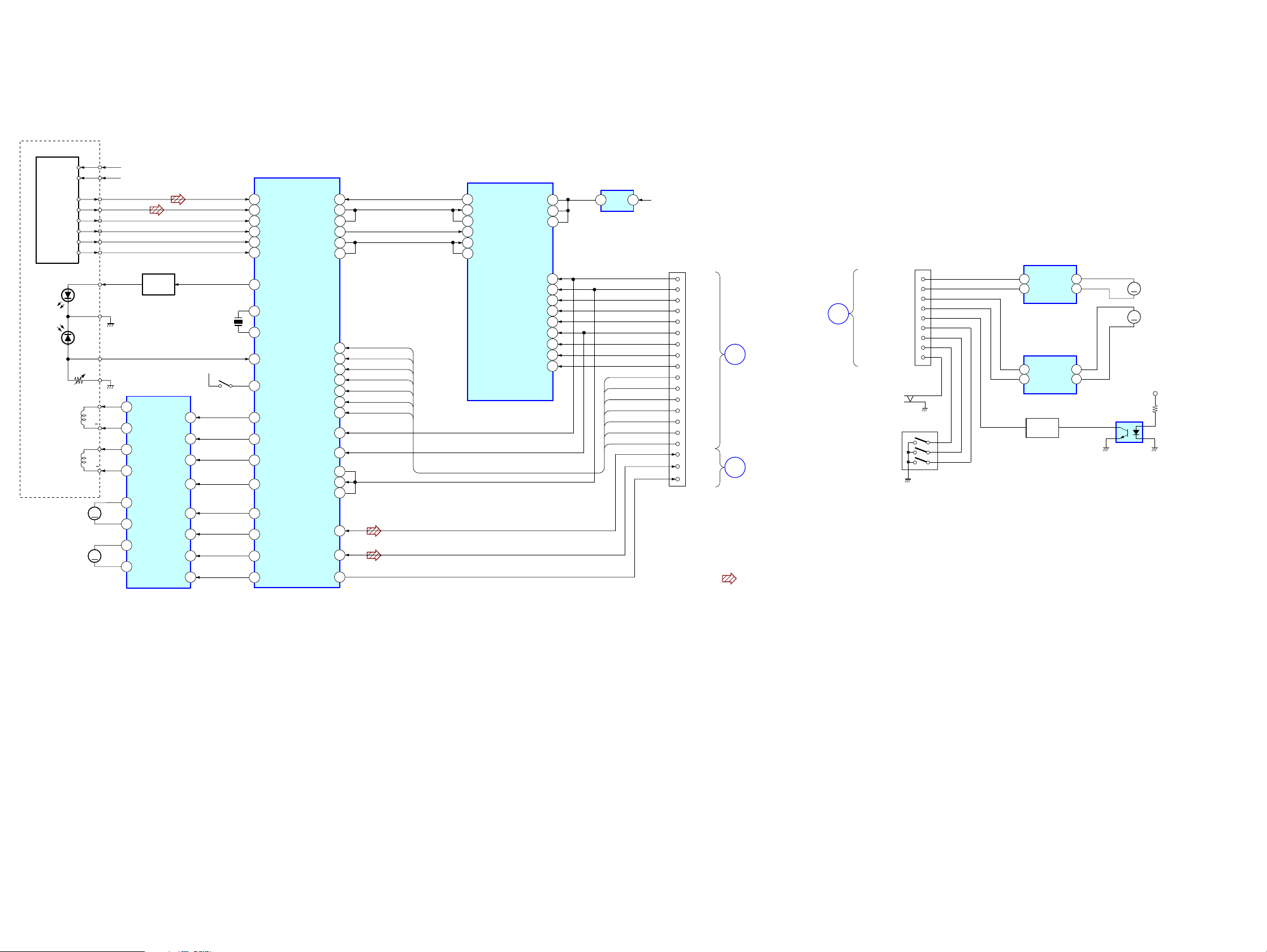
HCD-GX450
– BD/DRIVER SECTION –
OPTICAL PICK-UP
BLOCK
(KSM-215DCP/C2NP)
DETECTOR
VCC
FOCUS
COIL
TRACKING
COIL
(SPINDLE)
M102
(SLED)
VC
A
B
C
D
E
F
LD
GND
PD
VR
M101
+1.7V
+3.3V
Q10
DRIVER
IC251
SL/SP MOTOR
DRIVER
F+
16
CH2OUT-F
F
15
CH2OUT-R
T+
17
CH1OUT-R
T
18
CH1OUT-F
19
CH4OUT-F
M
20
CH4OUT-R
21
CH3OUT-R
M
CH3OUT-F
22
LD
CH1FIN
CH1RIN
CH2FIN
CH2RIN
SFDR
SRDR
OPIN+
MUTE
IC301
11
SDO0
16
LRCKIA
19
SFSY/LRCK1B
14
SDIO
15
BCKIA
18
SBSY/BCK1B
DIGITAL SIGNAL
PROCESSOR
PO11/BUCK/AD1
SRMSTB
VDD
VDD
VDDM
STANBY
MIACK
MICK
MIDIO
MILP
MICS
RESET
IC303
55
21
40
3
36
8
7
6
5
4
2
41
5 1
REG
SCOR
SENS
CLOCK
XLT
DATA
XRST
XTACN
3.3V
CN201
MP3STB
MP3REQ
MIACK
MICK
MIDIO
MILP
MICS
MP3RST
SRMSTB
SCOR
SENS
CLOCK
XLT
DATA
XRST
XTACN
LOUT
ROUT
DOUT
• R-CH is omitted due to same as L-CH
• Signal Path
PANEL
SECTION
A
MAIN
SECTION
B
: CD
MAIN
SECTION
D
LMR
LMF
TM-R
TM-F
TBL ADDRESS SW
E-1
E-2
E-3
OPEN SW
(LEVER SW)
E-3
E-2
E-1
CN701
S751
RE701
ROTARY
ENCODER
IC701
(LD)MOTOR DRIVER
RIN
OUT1
9
FIN
9
7
IC712
RIN
FIN
Q731
SWITCH
OUT2
OUT1
OUT2
11
TBL MOTOR DRIVER
4
2
4
2
M
M
IC731
(TABLE SENSOR)
M751(LOADING)
M741(TBL)
+3V
IC101
RF AMP
26
A
27
B
28
C
29
D
19
E
20
F
36
LD
XTAO
100
77
78
37
11
12
13
14
30
29
7
6
XTAI
PD
SSTP
TFDR
TRDR
FFDR
FRDR
CH3FIN
CH3RIN
MPD
XRST
X171
16.9MHz
+3.3V
SW101
5
6
7
8
9
10
3
24
PCMD1
LRCK1
LRCK
PCMD
BCK
BCK1
XTACN
XRST
DATA
XLAT
CLOCK
SENS
SCOR
GFS
C2PO
FOK
AOUT1
AOUT2
DOUT
100
102
104
105
107
115
113
114
61
62
63
65
66
60
95
1
2
3
81
86
71
XTACN
XRST
DATA
XLAT
CLOCK
SENS
SCOR
2424
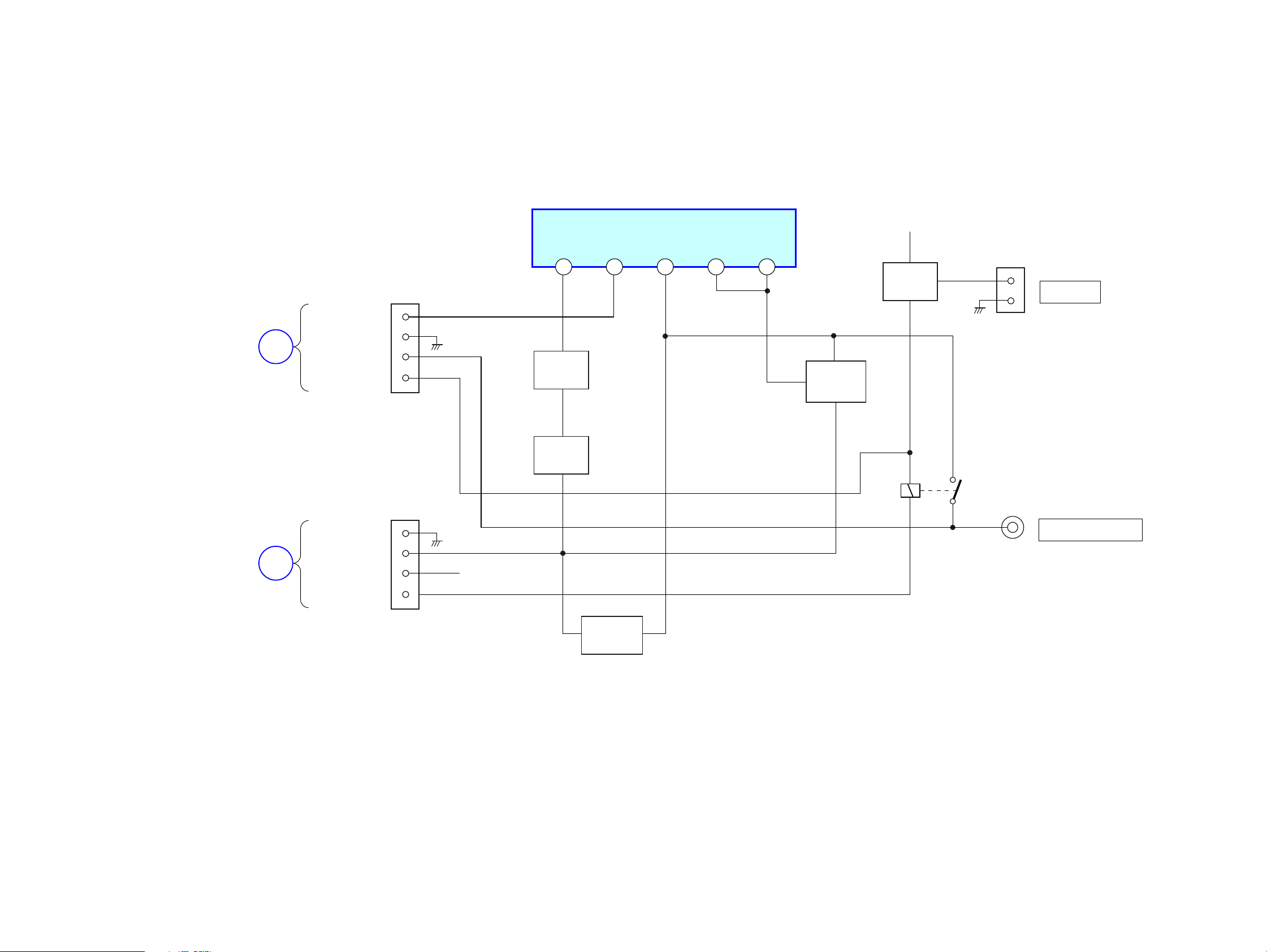
– SUB-WOOFER SECTION –
HCD-GX450
IC501
AMP
+B
MAIN
SECTION
MAIN
SECTION
C
E
CN501
SW-SIG-IN
GND
SW-LIMIT
SW-SENCE
CN502
GND
OVERLOAD/DC
RELAY+ +B
PT-2
2
Q507
DETECT
Q503
DETECT
SW IN
3
-RE
8 12
+RE
13
Q502
CN503
SWITCH
CONTROL
Q501
OVERCOAR
DETECT
RY501
JK501
SUB WOOFER OUT
RELAY-
Q506,Q505
DETECT
2525
HCD-GX450
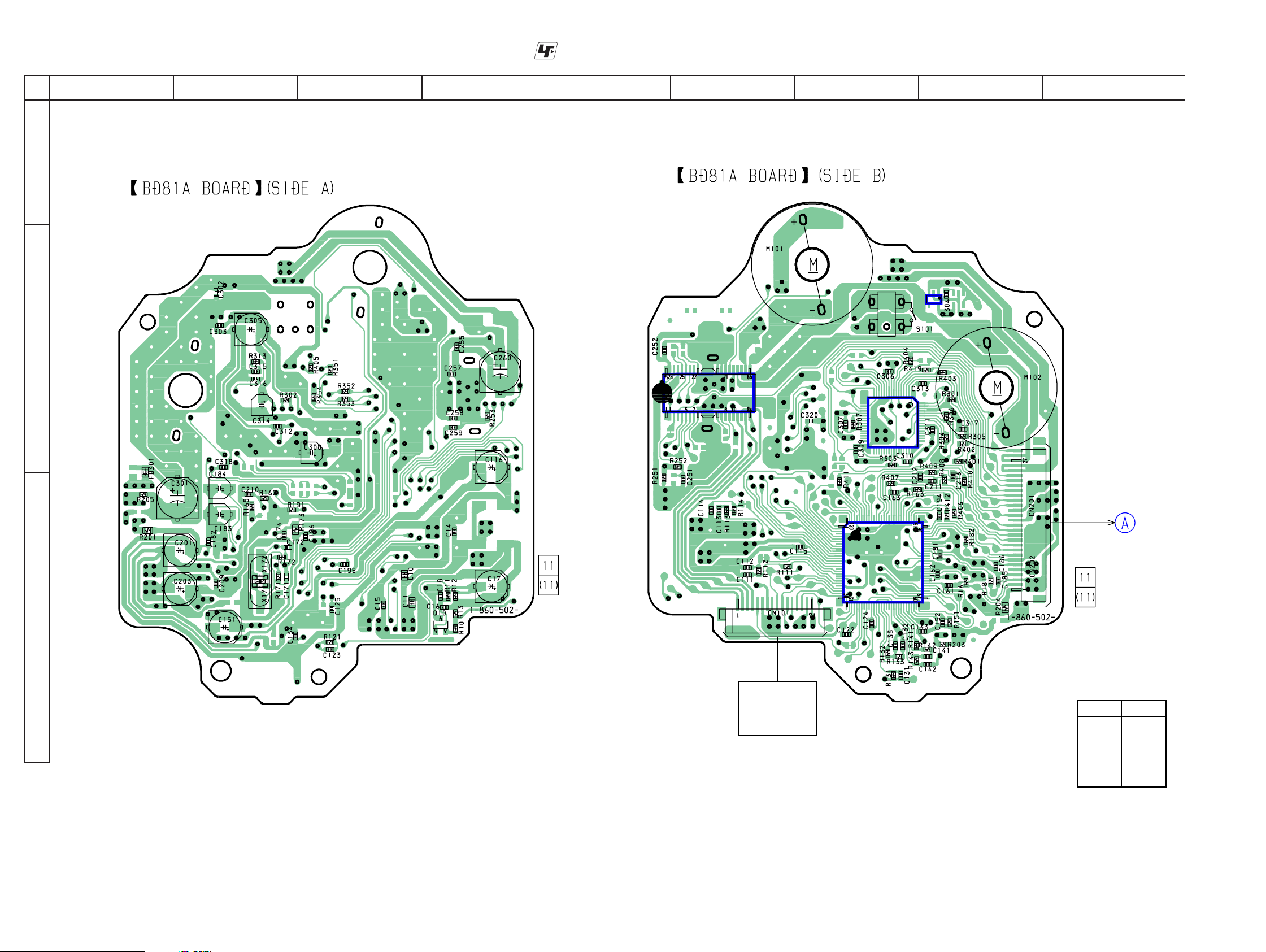
5-2. PRINTED WIRING BOARD – BD81A SECTION –
12
A
B
• See page 21 for Circuit Boards Location.
• : Uses unleaded solder .
3456789
SPINDLE
MOTOR
IC303
1
3
5
4
(LIMIT)
C
D
E
IC301
SLED
MOTOR
IC251
CONNECT
IC101
E
• Semiconductor
OPTICAL
PICK-UP
BLOCK
(KSM–215DCP)
BOARD
CN251
(Page 33)
Location
Ref. No. Location
IC101 D-7
IC251 C-6
IC301 C-7
IC303 B-7
Q10 E-4
2626
HCD-GX450
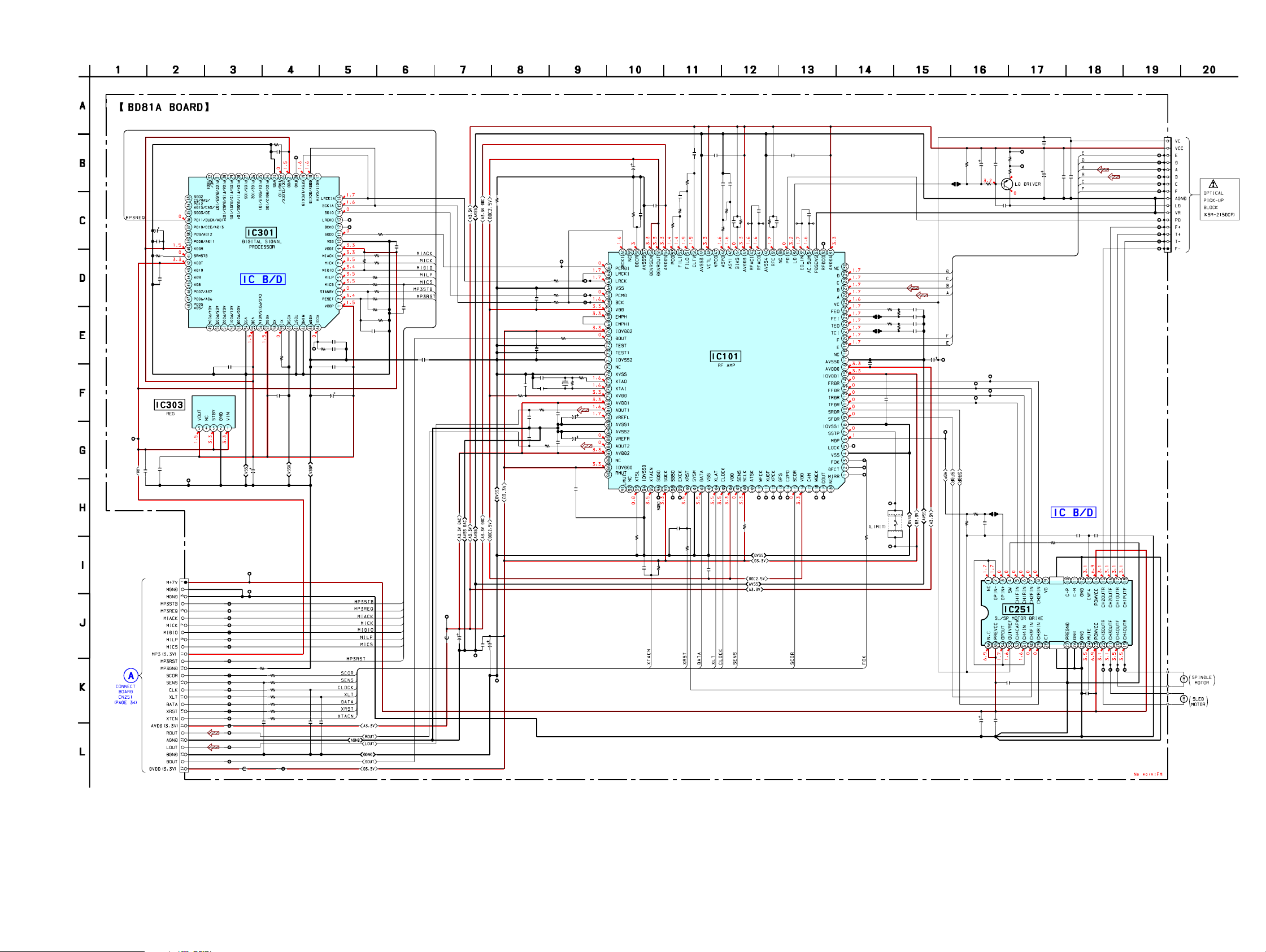
5-3. SCHEMATIC DIAGRAM – BD81A SECTION –
R307
10k
TP433
MP3VDD
FB301
BLM21B272S
0.1 F
C307
0.1 F
C308
47
4V
C309
R303
100k
C310
0.1 F
IC303
BH15FB1W
C302
C303
0.1
0.1
F
F
TP422
MP3GND
CN201
27P
C311
0.1 F
TP401
TP402
TP403
TP404
TP405
TP406
TP407
TP408
TP417
TP416
TP415
TP414
TP413
TP412
TP419
TP434
TP410
TP411
TP409
IC301
TC94A34FG-002
C305
TP186
MVDD
TP187
MGND
MP3STB
MP3REQ
MIACK
MICK
MIDIO
MILP
MICS
MP3RST
R205
SCOR
SENS
CLK
XLT
DATA
XRST
XTCN
AVDD
ROUT
LOUT
DOUT
R204
0
TP304
0.0022 B
TP
301
0
306
R
C312
0.1 F
220
4V
0
R411
R410
R409
R408
R407
R406
R412
C213
22p CH
R313
0.1 B
220
100
100
100
100
100
100
100
22p CH
C212
TP435
C211
DVDD
• See page 46 for IC PIN FUNCTION DESCRIPTION.
C10C11
C15
10
F
C13
NM
R253
10k
IC251
BA5947FM
(HSOP28)
10
6.3
6.3
B
B
C259
0.1
C258
F
0.1
+
L-
SL+
SP
S
3
5
252
251
TP
TP
TP2
F
57
C2
0.1
0.1
B
C134
0.1 F
015
C142
C151
100
10V
0
1
R203
0
TP302
TP303
R351
100
10k
R405
R404
R419
R403
R402
R401
R301
C317
0.01 B
0.1 F
47 4V
C306
0.1 F
100
100
100
100
100
100
C318
0.01
B
100k
R305
100k
C320
0
C174
0.1 F
TP436
AVDD
C201
100
0
10V
R201
TP420
AGND
C203
100
10V
B
209
C
0.01
TP421
DGND
TP427
PCMDI
TP103
LRCK
R352
100
R353
100
TP104
PCMD
R354
100
TP105
C161
0.1 F
R173
0
C185
2200p CH
R181
100
C186
2200p CH
BCK
R161
100
0.1 F
C162
R171C171
47022p CH
R172
1M
X171C172
16.9MHz27p CH
C181
0.1 F
22 6.3V
C183
22 6.3V
C184
R182
100
0.1 F
C182
C194
0.1
F
R302
C316
C315
C313
C314
220p CH
51
1
R
165
R
C210
0.1 B
152
C
C143
0.1 F
2
14
TP
0
0.0
43
3.3k
R1
B
141
C
0.1
142
1k
R
4.7k
141
R
CK
SO
148
EX
SB
TP
TP149
C163
0.1
3
0
16
10
R
R162
47k
B
0.01
33
C1
33
R1
132
R
IC101
CXD3059AR
0.1
196
C
B
132
C
0.47
H
C
I
100p
1M
FAC
R
0k
131
131
5
18
R
C
TP12
0k
1
0
191
R
C125
0.1 F
H
C
B
O
C124
30p
15k
0.1
3
FAC
R
R121
124
TP
K
F
4
G
FC
145
U
X
W
TP14
TP
22
B
0.1
C1
C123
47
CK
153
XP
P
TP1
T
2
123
12
TP
TP
O
21
FDC
P1
R
T
R111
1k
C111
0.0033 B
R112
15k
C112
470p
C113
JPO102
JPO103
0.1 F
C115
TP167
LOCK
TP178
FOK
TP166
DFCT
TP165
MIRR
46
PO
C2
GFS
TP1
T
CK
62
U
D
160
O
P1
C
W
TP
T
R193
NM
0.0033
FEI
R114
R113
TEI
S101
SW
15k
1k
C114
470p B
C116
100
10V
0.1 F
C195
5
+
42
SW
TP
-
26
W
S
P4
T
C17
R12
220
100k
4V
JPO10
TP177
VC
TP432
MDP
R11
APC
TP429
FFDR
TP431
TFDR
R251
10k
C260
220 10V
0
TP428
TP430
JPO004
R252
MDP
22k
C251
0.0068
TP423
IOP1
C16
R13
1
1
F
TP424
IOP2
R10
3.3
Q10
2SB1690K
C18
0.001 B
FRDR
TRDR
B
C252
0.1 F
C255
0.1 F
CN101
16P
E
TP10
D
TP11
A
TP12
B
TP13
C
TP14
F
TP102
PD
TP15
F+
TP16
F-
TP17
T-
TP18
F-
TP19
0
P
25
S
TP
M101
M102
2727
HCD-GX450
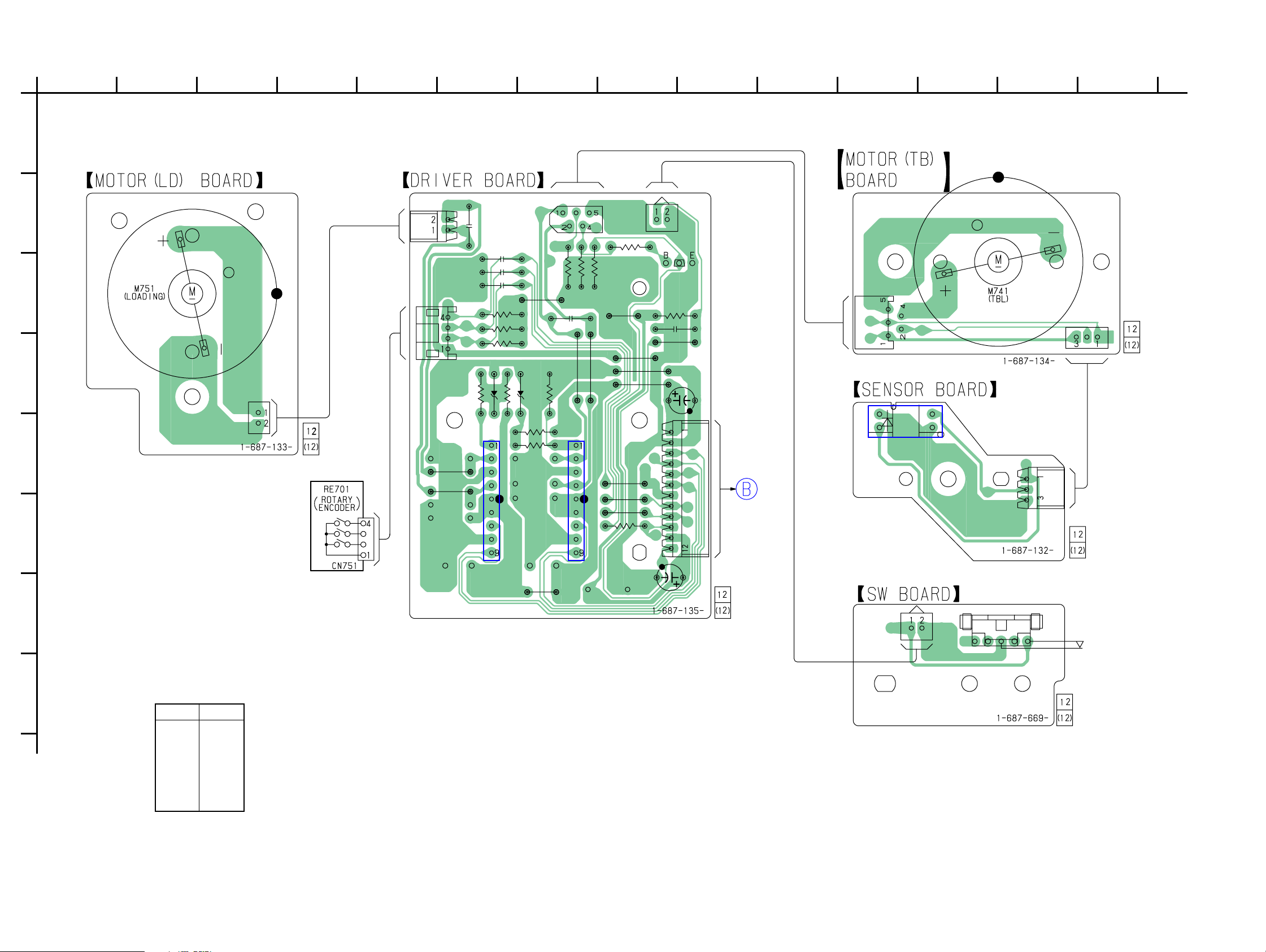
5-4. PRINTED WIRING BOARD – CD MECHANISM SECTION –
1
234567891011121314
A
B
C
D
• See page 21 for Circuit Boards Location.
CN704
C751
C737
C736
C735
JW710
R723
R722
CN703
R721
R702
D701
R701
D711
C741
R713
CN702
R735
JW709
R734
JW708
R732
R733
JW711
JW707
JW706
JW705
CN705
JW712
Q731
R751
C752
CN741
CN742
C715
E
F
G
H
• Semiconductor
Location
Ref. No. Location
D701 D-6
D711 D-7
CN721
JW713
JW714
IC701
R711
R712
JW701
IC712
JW704
JW703
JW702
R731
C731
CN701
MAIN
BOARD
CN301
(Page 30)
IC731
CN751
CN731
S751
(LEVER SW)
IC701 F-6
IC712 F-7
IC731 E-11
Q731 C-9
2828
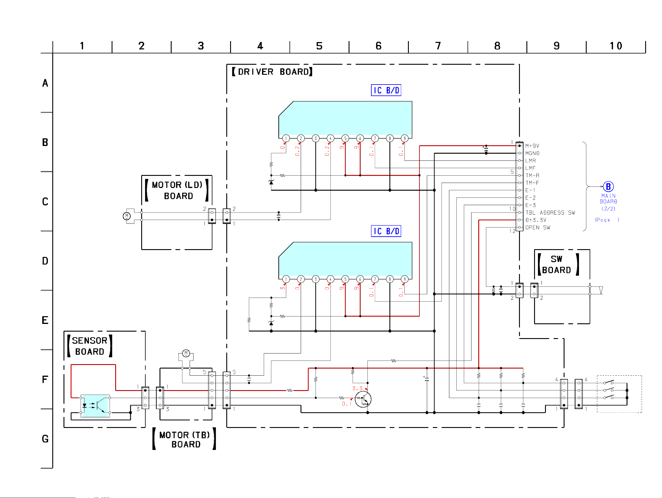
5-5. SCHEMATIC DIAGRAM – CD MECHANISM SECTION –
HCD-GX450
IC701
BA6956AN
LD MOTOR
DRIVER
M751
(LOADING)
CN721
2P
CN704
2P
R713
22k
R702
100
MTZJ-T-77-5.1A
R712
4.7k
D701
R701
470
C751
0.01
R711
1k
VREF
VREF
OUT2
OUT2
RNF
RNF
OUT1
VM
IC712
BA6956AN
TBL MOTOR
DRIVER
OUT1
VM
VCC
VCC
FIN
FIN
GND
GND
RIN
RIN
C715
100
16V
R751
4.7k
C752
0.1
CN705
2P
CN701
12P
CN301
32
S751
(LEVER SW)
CN751
2P
IC731
RPI-576
TABLE
SENSOR
CN731
3P
CN741
3P
M741
(TBL)
CN742
5P
C741
0.01
CN702
5P
D711
MTZJ-T-77-3.6B
R735
100
R734
12k
R733
1k
R732
10k
DTC114ESA
TBL ADDRES
SENS SWITCH
2929
R731
100
Q731
C731
10
50V
R721
4.7k
C735
0.1
R722
4.7k
C736
0.1
no mark : FM
R723
4.7k
C737
0.1
CN703
4P
CN751
4P
RE701
ROTARY
ENCODER
E-3
E-2
E-1
HCD-GX450
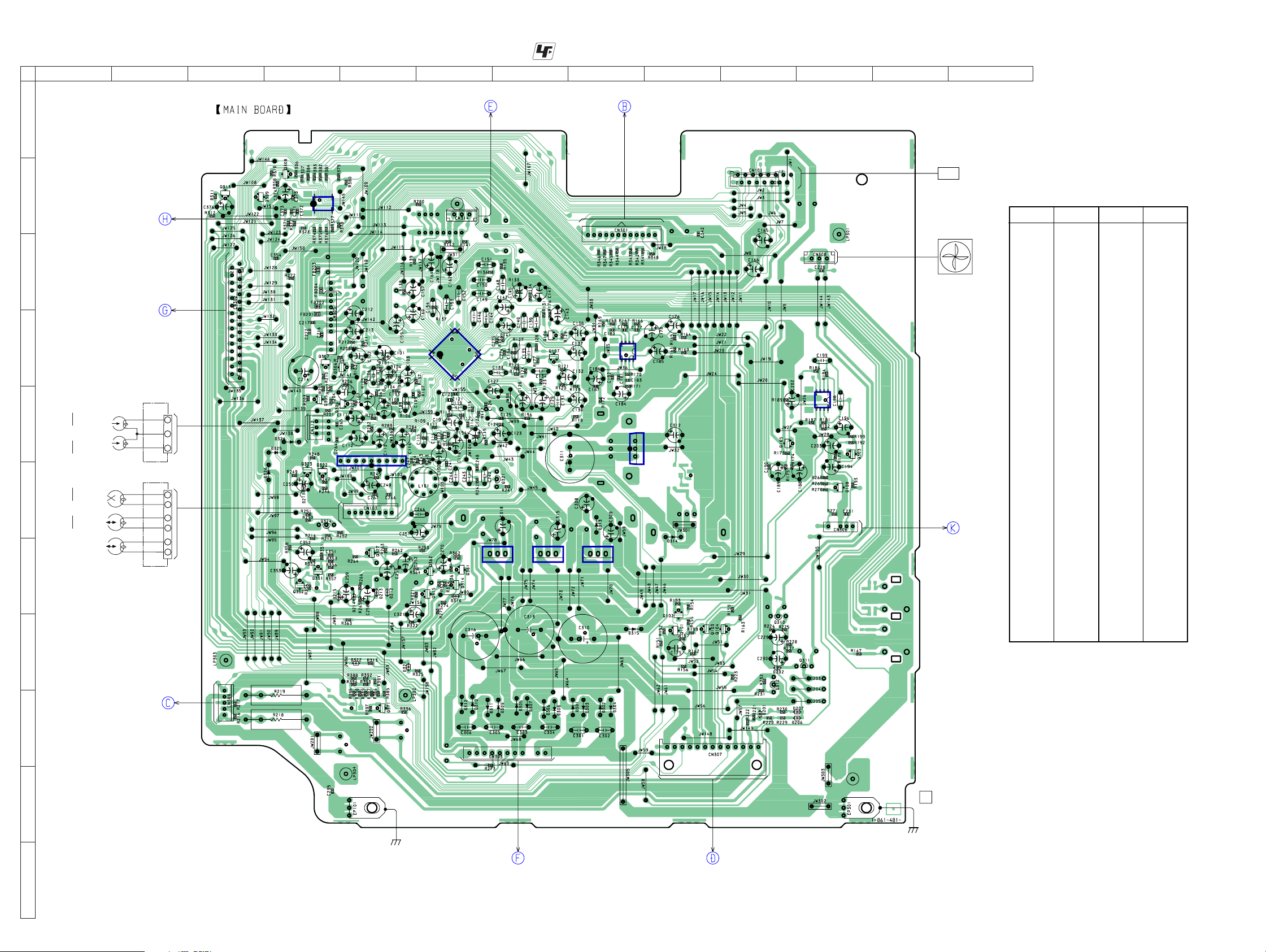
5-6. PRINTED WIRING BOARD – MAIN SECTION –
12
345678910111213
A
B
CONNECT
BOARD
CN254
(Page 33)
E
E
C
PANEL
BOARD
CN601
D
ERASE
HEAD
L CH
R CH
HP1
R CH
L CH
HP2
HE1
HRP2
HRP1
E
F
PB
HEAD
REC/PB
HEAD
(Page 37)
DECK-A
(PLAY)
DECK-B
(REC/PLAY)
28
29
1
2
3
1
2
3
4
3
4
G
H
1
• See page 21 for Circuit Boards Location.
E
IC371
10
E
E
E
E
3
1
IC201
91
E
E
1
E
E
E
E
9
1
33
6
8
E
E
3
IC101
E
E
1
GAMEJACK
(Page 33)
E
1
IC304
• : Uses unleaded solder.
BOARD
CN801
1
E
E
3
1
IC303
1
3
IC301
3
IC102
DRIVER
BOARD
CN701
(Page 28)
1
3
12
IC302
TUNER
• Semiconductor Location
Ref. No. Location
FAN
1
3
D201 I-10
D202 H-10
D203 H-11
D204 H-11
D205 I-11
D206 I-10
D207 I-10
D211 F-4
D212 G-5
D213 G-5
D214 G-5
D215 G-4
D301 I-8
D302 I-8
IC104
D303 I-8
D304 I-8
D305 I-7
D306 I-7
D307 I-7
E
D308 I-7
D309 I-7
E
D310 I-6
D311 I-6
D312 I-6
E
D313 F-8
D314 F-9
D315 H-8
1
4
SUB-WOOFER
BOARD
CN501
(Page 35)
D316 G-6
D321 H-5
D322 H-5
D324 E-4
D325 E-4
D326 F-4
E
E
E
E
E
E
E
IC101 D-6
IC102 D-8
IC104 D-11
IC201 E-5
Ref. No. Location
IC301 G-8
IC302 E-9
IC303 G-7
IC304 G-7
IC371 B-4
Q101 H-9
Q102 H-9
Q103 H-9
Q104 H-10
Q105 E-10
Q106 D-7
Q107 D-7
Q108 F-11
Q303 E-11
Q304 E-4
Q305 E-4
Q306 B-4
Q307 B-4
Q308 B-4
Q309 B-3
Q310 H-10
Q311 H-11
Q312 H-10
Q313 B-3
Q314 G-6
Q315 G-6
Q321 F-7
Q322 F-4
Q323 F-4
Q324 F-4
Q327 G-5
Q351 G-4
Q352 G-4
Q361 G-6
Q362 G-6
Q371 I-5
H/P JACK
I
BOARD
CN804
(Page 33)
5
J
K
E
(CHASSIS)
11
1
13
1
12
(CHASSIS)
TRANS
BOARD
CN907
(Page 40)
AMP
BOARD
CN441
(Page 41)
3030
 Loading...