

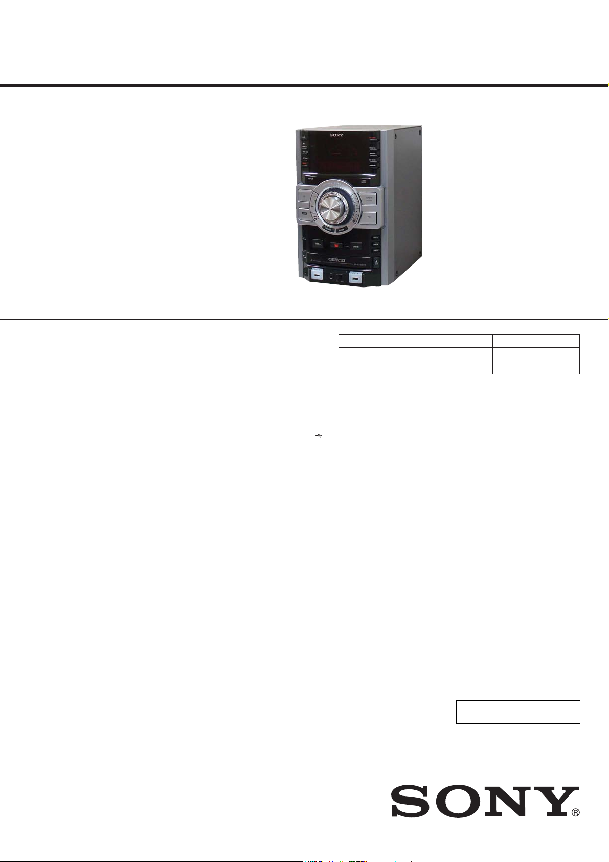
HCD-GTZ4/GTZ4i/GTZ5
SERVICE MANUAL
Ver. 1.1 2009.08
• HCD-GTZ4 is the amplifi er, USB, Disc player, tuner and
iPod section in MHC-GTZ4.
• HCD-GTZ4i is the amplifi er, USB, Disc player, tuner and
iPod section in LBT-GTZ4i, MHC-GTZ4i.
• HCD-GTZ5 is the amplifi er, USB, Disc player, tuner and
iPod section in MHC-GTZ5. Photo: HCD-GTZ5
“WALKMAN” and “WALKMAN”
logo are registered trademarks of
Sony Corporation.
MICROVAULT is a trademark of
Sony Corporation.
MPEG Layer-3 audio coding technology and patents licensed from Fraunhofer IIS and Thomson.
Windows Media is a registered trademark of Microsoft Corporation in the
United States and/or other countries.
“Memory Stick” is a trademark of
Sony Corporation.
iPod is a trademark of Apple Inc., registered in the U.S. and other countries.
AUDIO POWER SPECIFICATION
POWER OUTPUT AND TOTAL HARMONIC
DISTORTION:
(HCD-GTZ4i: US model only)
With 6 ohm loads, both channels driven, from
120 Hz – 10 kHz; rated 110 watts per channel minimum RMS
power, with no more than 0.7% total harmonic distortion from
250 miliwatts to rated output.
Amplifier section
HCD-GTZ5
The following are measured at
Mexican model:
AC 127 V, 60 Hz
Other models:
AC 120, 220, 240 V, 50/60 Hz
Front speaker
Power output (rated): 110 W + 110 W
(at 6 :, 1 kHz, 1% THD)
RMS output power (reference):
200 W + 200 W (per channel at 6 :, 1 kHz, 10% THD)
Subwoofer
RMS output power (reference): 200 W
(at 6 :, 100 Hz, 10% THD)
HCD-GTZ4i (US model)
The following are measured at AC 120 V 60 Hz
Front speaker
RMS output power (reference):
::SHUFKDQQHODWN+]7+'
Subwoofer
RMS output power (reference): 180 W
DW+]7+'
HCD-GTZ4 / GTZ4i
(AEP, Australian, Argentina models)
The following are measured at
European model:
AC 230 V, 50 Hz
Other models:
AC 120, 220, 240 V, 50/60 Hz
Front speaker
Power output (rated): 90 W + 90 W
(at 6 :, 1 kHz, 1% THD)
RMS output power (reference):
155 W + 155 W (per channel at 6 :, 1 kHz, 10% THD)
Subwoofer
RMS output power (reference): 150 W
(at 6 :, 100 Hz, 10% THD)
Model Name Using Similar Mechanism NEW
Mechanism Type CDM88B-DVBU101
Optical Pick-up Block Name KHM-313CAB
SPECIFICATIONS
Inputs
PC (AUDIO IN) L/R:
Voltage 700 mV
impedance 47 kilohms
MIC: sensitivity 1 mV, impedance 10 kilohms
(USB) port: Type A
Outputs
PHONES: accepts headphones of 8 : or more
FRONT SPEAKER: accepts impedance of 6 :
SUBWOOFER: accepts impedance of 6 :
USB section
Supported bit rate
MP3 (MPEG 1 Audio Layer-3):
32 – 320 kbps, VBR
WMA: 48 – 192 kbps
AAC: 48 – 320 kbps
Sampling frequencies
MP3 (MPEG 1 Audio Layer-3):
32/44.1/48 kHz
WMA: 44.1 kHz
AAC: 44.1 kHz
Transfer speed
Full-Speed
Supported USB device
Mass Storage Class
Maximum current
500 mA
Disc player section
System
Compact disc and digital audio system
Laser Diode Properties
Emission Duration: Continuous
Laser Output*: Less than 44.6 PW
* This output is the value measurement at a distance of
200 mm from the objective lens surface on the Optical
Pick-up Block with 7 mm aperture.
Frequency response
20 Hz – 20 kHz
Signal-to-noise ratio
More than 90 dB
Dynamic range
More than 88 dB
Tuner section
FM stereo, FM/AM superheterodyne tuner
US Model
AEP Model
Australian Model
HCD-GTZ4i
E Model
HCD-GTZ4/GTZ5
FM tuner section
Tuning range:
North American model:
87.5 – 108.0 MHz (100 kHz step)
Other models:
87.5 – 108.0 MHz (50 kHz step)
Antenna: FM lead antenna
Antenna terminals: 75 ohms unbalanced
Intermediate frequency: 10.7 MHz
AM tuner section
Tuning range
Pan American and Oceanian models:
530 – 1,710 kHz (with 10 kHz tuning interval)
531 – 1,710 kHz (with 9 kHz tuning interval)
European models:
531 – 1,602 kHz (with 9 kHz tuning interval)
Other models:
530 – 1,610 kHz (with 10 kHz tuning interval)
531 – 1,602 kHz (with 9 kHz tuning interval)
Antenna: AM loop antenna, external antenna terminal
Intermediate frequency: 450 kHz
iPod section
DC5V 500mA MAX
General
Power requirements
North American model: AC 120 V, 60 Hz
European models: AC 230 V, 50/60 Hz
Oceanian model: AC 230 – 240 V, 50/60 Hz
Mexican model: AC 127 V, 60 Hz
Argentine model: AC 220 V, 50/60 Hz
Other models: AC 120, 220 or 230 – 240 V, 50/60 Hz,
Adjustable with voltage selector
Power consumption
MHC-GTZ5: 250 W
HCD-GTZ4i (American model): 240W
MHC-GTZ4 / GTZ4i (Other models): 300 W
Dimensions (w/h/d) (excl. speakers)
Approx. 231 × 361 × 430.5 mm
(9 1/8 × 14 1/4 × 17 1/4 inch)
Mass (excl. speakers)
HCD-GTZ5 / GTZ4 / GTZ4i:
10.0 kg (22 lb 1 oz)
Design and specifications are subject to change wit hout notice.
6WDQGE\SRZHUFRQVXPSWLRQ:
+DORJHQDWHGIODPHUHWDUGDQWVDUHQRWXVHGLQWKHFHUWDLQ
printed wiring boards.
9-889-503-02
2009H05-1
2009.08
©
COMPACT DISC RECEIVER
Sony Corporation
Audio&Video Business Group
Published by Sony Techno Create Corporation
HCD-GTZ4/GTZ4i/GTZ5
Ver. 1.1
NOTES ON CHIP COMPONENT REPLACEMENT
• Never reuse a disconnected chip component.
• Notice that the minus side of a tantalum capacitor may be damaged by heat.
FLEXIBLE CIRCUIT BOARD REPAIRING
• Keep the temperature of soldering iron around 270 °C during
repairing.
• Do not touch the soldering iron on the same conductor of the
circuit board (within 3 times).
• Be careful not to apply force on the conductor when soldering
or unsoldering.
SAFETY CHECK-OUT
After correcting the original service problem, perform the following safety check before releasing the set to the customer:
Check the antenna terminals, metal trim, “metallized” knobs,
screws, and all other exposed metal parts for AC leakage.
Check leakage as described below.
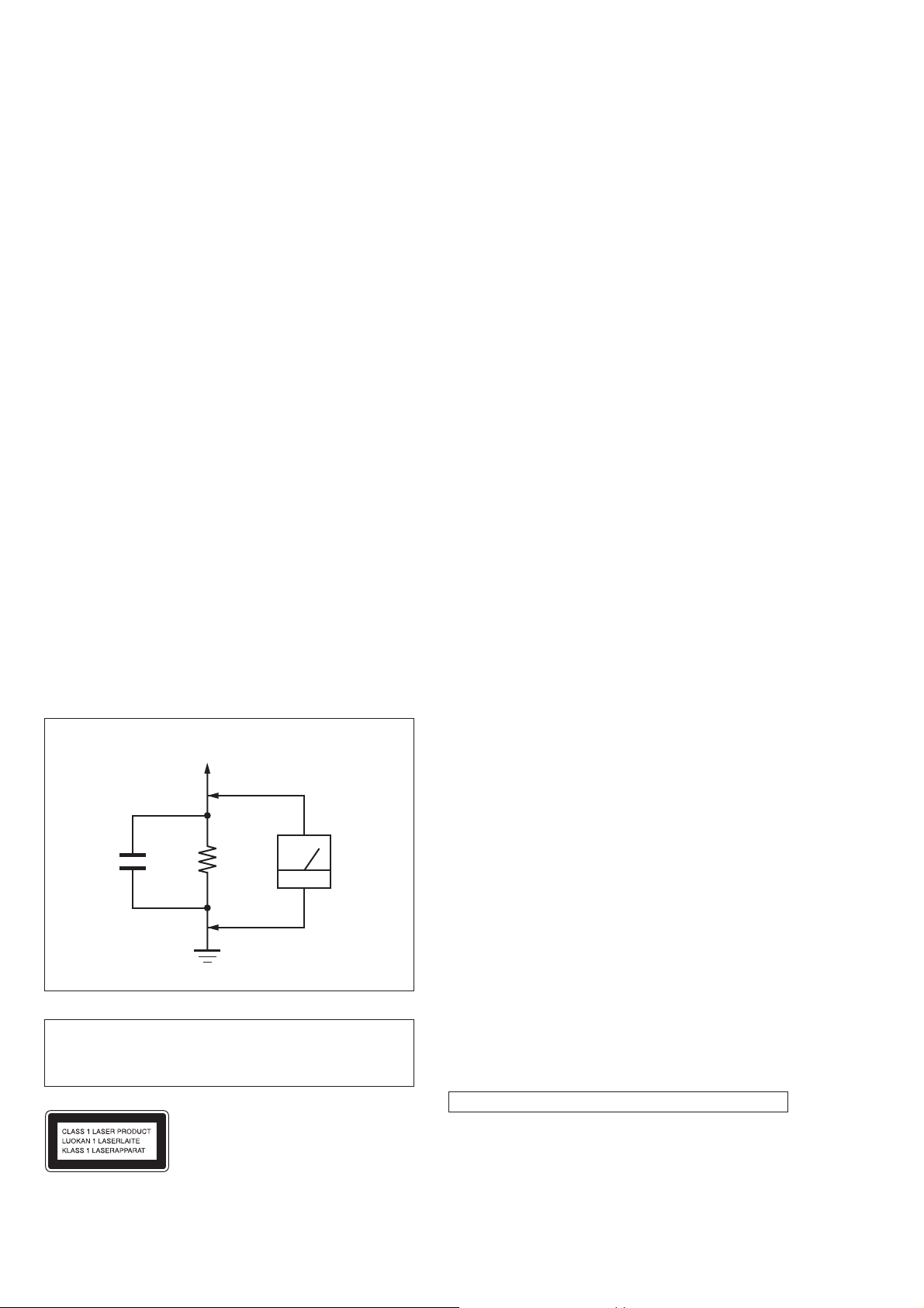
LEAKAGE TEST
The AC leakage from any exposed metal part to earth ground and
from all exposed metal parts to any exposed metal part having a
return to chassis, must not exceed 0.5 mA (500 microamperes.).
Leakage current can be measured by any one of three methods.
1. A commercial leakage tester, such as the Simpson 229 or RCA
WT-540A. Follow the manufacturers’ instructions to use these
instruments.
2. A battery-operated AC milliammeter. The Data Precision 245
digital multimeter is suitable for this job.
3. Measuring the voltage drop across a resistor by means of a
VOM or battery-operated AC voltmeter . The “limit” indication
is 0.75 V, so analog meters must have an accurate low-voltage
scale. The Simpson 250 and Sanwa SH-63Trd are examples
of a passive VOM that is suitable. Nearly all battery operated
digital multimeters that have a 2 V AC range are suitable. (See
Fig. A)
To Exposed Metal
Parts on Set
AC
1.5 kΩ0.15 μF
Earth Ground
voltmeter
(0.75 V)
Fig. A. Using an AC voltmeter to check AC leakage.
CAUTION
Use of controls or adjustments or performance of procedures
other than those specifi ed herein may result in hazardous radia-
tion exposure.
TABLE OF CONTENTS
1. SERVICING NOTES ............................................. 3
2. DISASSEMBLY
2-1. Disassembly Flow ........................................................... 4
2-2. Case (Side-L/R) .............................................................. 4
2-3. Top Case.......................................................................... 5
2-4. Front Panel Block ........................................................... 5
2-5. DC Fan (M101) ............................................................... 6
2-6. Back Panel ...................................................................... 6
2-7. MAIN Board ................................................................... 7
2-8. DC Fan (M102), POWER AMP Board ........................... 7
2-9. HUB Board, DMB19 Board ........................................... 8
2-10. CD Mechanism Block (CDM88B-DVBU101) ............... 8
2-11. Optical Pick-up Block (KHM-313CAB) ........................ 9
2-12. Belt (DLM3A) ................................................................ 9
3. TEST MODE ............................................................ 10
4. ELECTRICAL CHECK ......................................... 12
5. DIAGRAMS
5-1. Block Diagram - RF SERVO, USB Section - ................. 13
5-2. Block Diagram - MAIN Section - ................................... 14
5-3. Block Diagram - AMP Section - ..................................... 15
5-4. Block Diagram
- PANEL, POWER SUPPLY Section - ........................... 16
5-5. Printed Wiring Board - DMB19 Board - ........................ 18
5-6. Schematic Diagram - DMB19 Board (1/3) - .................. 19
5-7. Schematic Diagram - DMB19 Board (2/3) - .................. 20
5-8. Schematic Diagram - DMB19 Board (3/3) - .................. 21
5-9. Printed Wiring Board - MAIN Board - ........................... 22
5-10. Schematic Diagram - MAIN Board (1/3) - ..................... 23
5-11. Schematic Diagram - MAIN Board (2/3) - ..................... 24
5-12. Schematic Diagram - MAIN Board (3/3) - ..................... 25
5-13. Printed Wiring Board - HUB Board - ............................. 26
5-14. Schematic Diagram - HUB Board - ................................ 27
5-15. Printed Wiring Board - POWER AMP Board - .............. 28
5-16. Schematic Diagram - POWER AMP Board - ................. 29
5-17. Printed Wiring Board - DISPLAY Board - ..................... 30
5-18. Schematic Diagram - DISPLAY Board - ........................ 31
5-19. Printed Wiring Boards - PANEL Section - ..................... 32
5-20. Schematic Diagram - PANEL Section - .......................... 33
5-21. Printed Wiring Board - TRANS Board - ......................... 34
5-22. Schematic Diagram - TRANS Board - ........................... 35
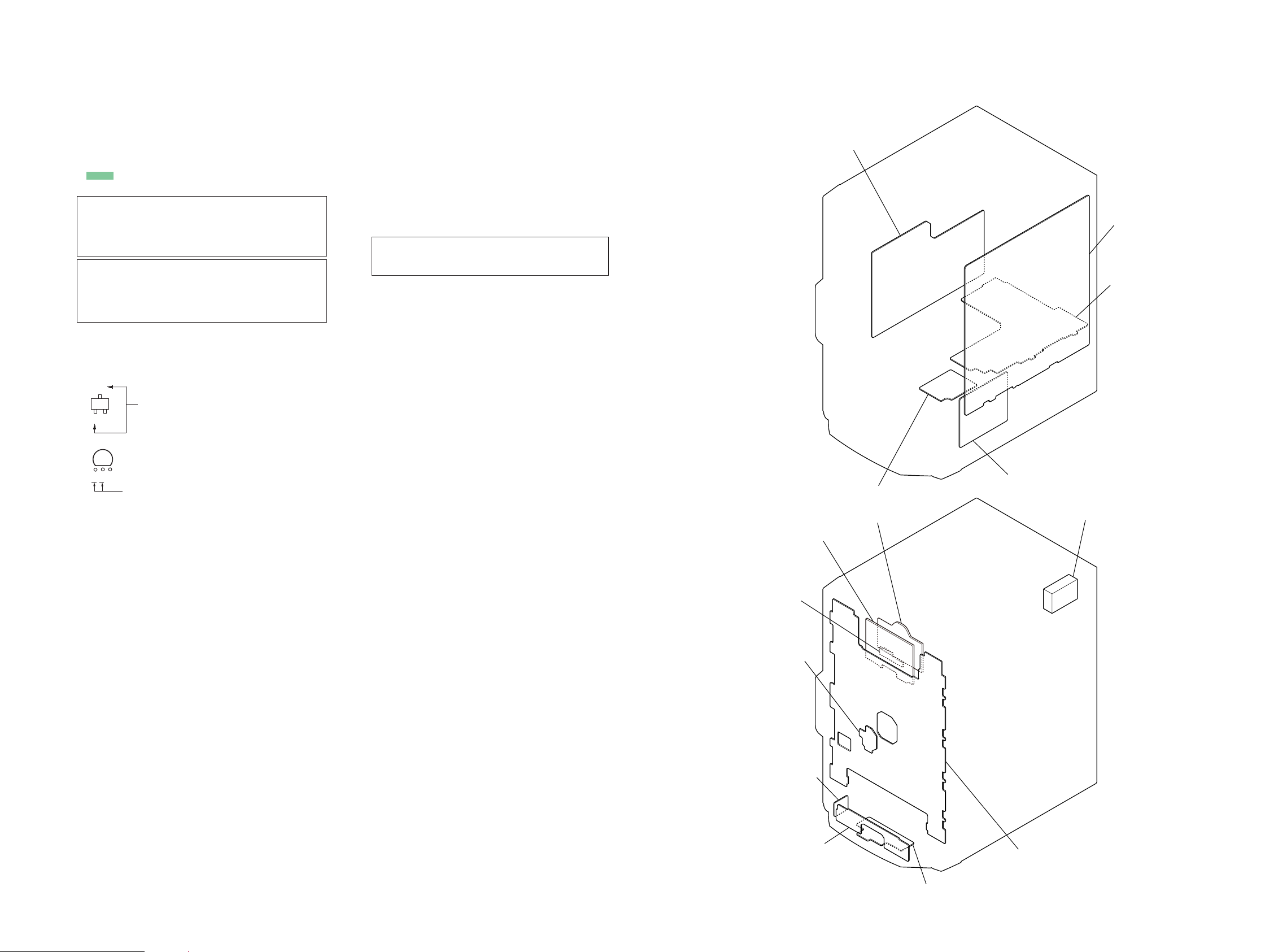
6. EXPLODED VIEWS
6-1. Case Section .................................................................... 44
6-2. Loading Panel Section .................................................... 45
6-3. DISPLAY Board Section ................................................ 46
6-4. Front Panel Section ......................................................... 47
6-5. Back Panel Section ......................................................... 48
6-6. MAIN Board Section ...................................................... 49
6-7. Chassis Section ............................................................... 50
6-8. CD Mechanism Section (CDM88B-DVBU101) ............ 51
7. ELECTRICAL PARTS LIST .............................. 52
This appliance is classified as a CLASS 1
LASER product. This marking is located on
the rear exterior.
2
Accessories are given in the last of the electrical parts list.
SAFETY-RELATED COMPONENT WARNING!
COMPONENTS IDENTIFIED BY MARK 0 OR DOTTED LINE
WITH MARK 0 ON THE SCHEMATIC DIAGRAMS AND IN
THE PARTS LIST ARE CRITICAL TO SAFE OPERATION.
REPLACE THESE COMPONENTS WITH SONY PARTS
WHOSE PART NUMBERS APPEAR AS SHOWN IN THIS
MANUAL OR IN SUPPLEMENTS PUBLISHED BY SONY.
SECTION 1
SERVICING NOTES
HCD-GTZ4/GTZ4i/GTZ5
Ver. 1.1
NOTES ON HANDLING THE OPTICAL PICK-UP
BLOCK OR BASE UNIT
The laser diode in the optical pick-up block may suffer electrostatic break-down because of the potential difference generated by
the charged electrostatic load, etc. on clothing and the human body .
During repair, pay attention to electrostatic break-down and also
use the procedure in the printed matter which is included in the
repair parts.
The fl exible board is easily damaged and should be handled with
care.
NOTES ON LASER DIODE EMISSION CHECK
The laser beam on this model is concentrated so as to be focused
on the disc refl ective surface by the objective lens in the optical
pickup block. Therefore, when checking the laser diode emission,
observe from more than 30 cm away from the objective lens.
UNLEADED SOLDER
Boards requiring use of unleaded solder are printed with the leadfree mark (LF) indicating the solder contains no lead.
(Caution: Some printed circuit boards may not come printed with
the lead free mark due to their particular size)
: LEAD FREE MARK
Unleaded solder has the following characteristics.
• Unleaded solder melts at a temperature about 40 °C higher
than ordinary solder.
Ordinary soldering irons can be used but the iron tip has to be
applied to the solder joint for a slightly longer time.
Soldering irons using a temperature regulator should be set to
about 350 °C.
Caution: The printed pattern (copper foil) may peel away if
the heated tip is applied for too long, so be careful!
• Strong viscosity
Unleaded solder is more viscous (sticky, less prone to fl ow)
than ordinary solder so use caution not to let solder bridges
occur such as on IC pins, etc.
• Usable with ordinary solder
It is best to use only unleaded solder but unleaded solder may
also be added to ordinary solder.
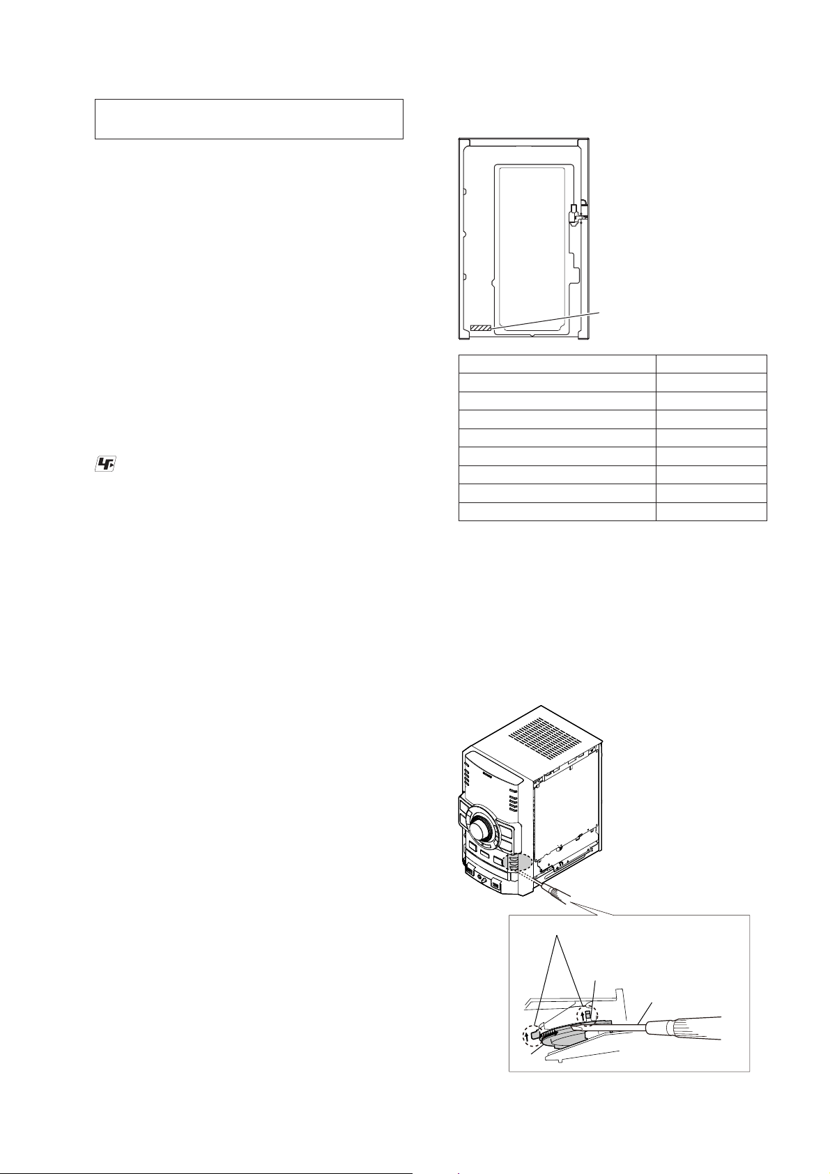
MODEL IDENTIFICATION
– Back Panel –
PART No.
Model Part No.
HCD-GTZ5: E2, E51
HCD-GTZ5: AR
HCD-GTZ5: MX
HCD-GTZ4: E2, E51
HCD-GTZ4: AR
HCD-GTZ4i: AUS
HCD-GTZ4i: AEP
HCD-GTZ4i: US
• Abbreviation
AR : Argentina model
AUS : Australian model
E2 : 120V AC area in E model
E51 : Chilean and Peruvian models
MX : Mexican model
4-124-494-0[]
4-124-494-1[]
4-124-494-3[]
4-131-035-0[]
4-131-035-1[]
4-131-035-6[]
4-131-035-7[]
4-131-035-8[]
HOW TO OPEN THE TRAY WHEN POWER SWITCH
TURN OFF
Note: Work after removing the case (side-R) referring to “2-2. CASE
(SIDE-L/R)” on disassembly (page 4).
NOTE OF REPLACING THE IC102 ON THE DMB19
BOARD
IC102 on the DMB19 board cannot exchange with single. When
this part is damaged, exchange the entire mounted board.
RELEASING THE DISC TRAY LOCK
The disc tray lock function for the antitheft of an demonstration
disc in the store is equipped.
Releasing Procedure:
1. Press [I/
STANDBY] button to turn the power on.
1
2. Press the [CD] button to select CD function.
3. While pressing the [
] button, press the [Z OPEN/CLOSE]
x
button for more 5 seconds).
4. The message “UNLOCKED” is displayed and the disc tray is
unlocked.
Note: When “LOCKED” is displayed, the slot lock is not released by
turning power on/off with the [I/
STANDBY] button.
1
state of opening the CD tray
1 Turn a gear by
a driver till a lever
lever
rises up to the
position of the figure.
gear
3
HCD-GTZ4/GTZ4i/GTZ5
Ver. 1.1
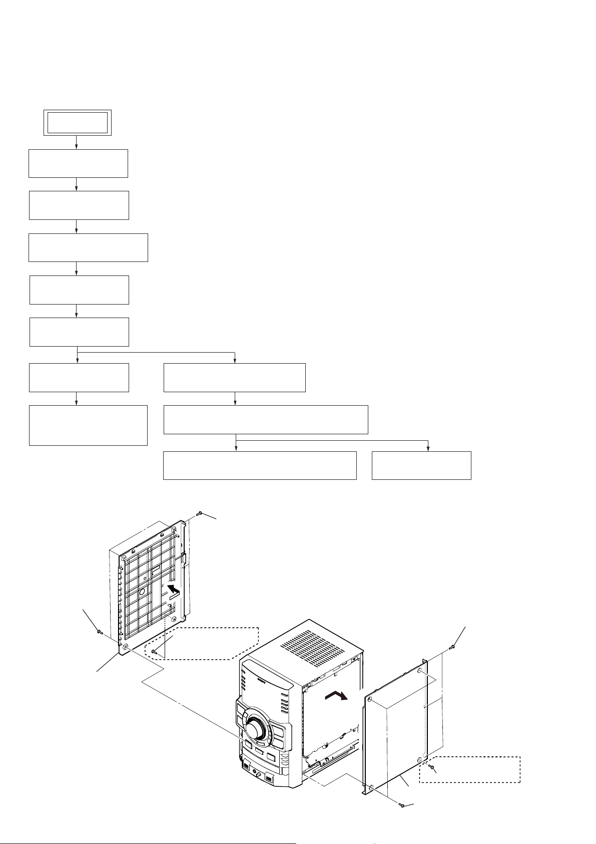
DISASSEMBLY
• This set can be disassembled in the order shown below.
2-1. DISASSEMBLY FLOW
SET
2-2. CASE (SIDE-L/R)
(Page 4)
2-3. TOP CASE
(Page 5)
2-4. FRONT PANEL BLOCK
(Page 5)
2-5. DC FAN (M101)
(Page 6)
SECTION 2
2-6. BACK PANEL
(Page 6)
2-7. MAIN BOARD
(Page 7)
2-8. DC FAN (M102),
POWER AMP BOARD
(Page 7)
Note: Follow the disassembly procedure in the numerical order given.
2-2. CASE (SIDE-L/R)
1 three screws
(case 3 TP2)
2-9. HUB BOARD, DMB19 BOARD
(Page 8)
2-10. CD MECHANISM BLOCK (CDM88B-DVBU101)
(Page 8)
2-11. OPTICAL PICK-UP BLOCK (KHM-313CAB)
(Page 9)
2 three screws
(BVTP3 u 8)
3
1 screw (case 3 TP2)
2-12. BELT (DLM3A)
(Page 9)
2 three screws
(BVTP3 u 8)
4 case (side-L)
4
(Mexican)
3
(Mexican)
1 screw (case 3 TP2)
4 case (side-R)
1 three screws
(case 3 TP2)
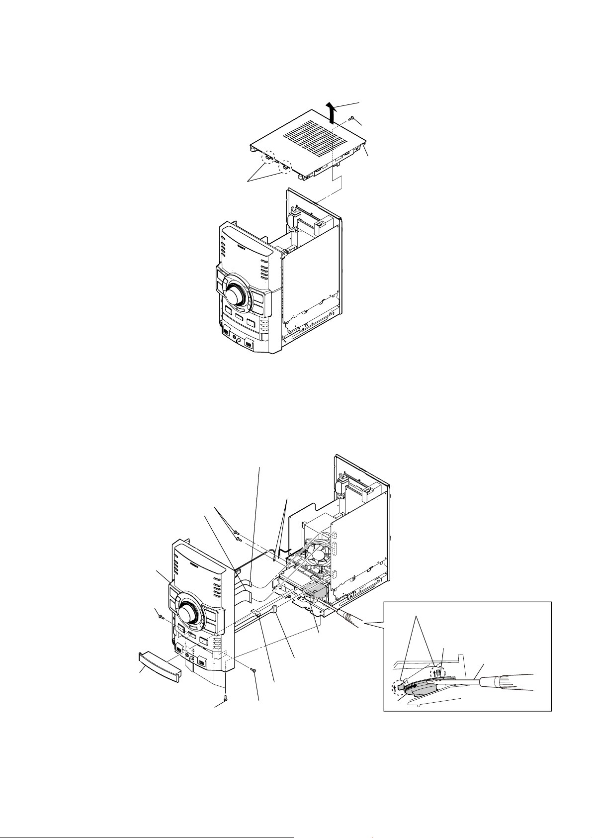
2-3. TOP CASE
HCD-GTZ4/GTZ4i/GTZ5
2 Lift up the back
side of top case.
1 screw
(BVTP3 u 8)
4 top case
3 two claws
2-4. FRONT PANEL BLOCK
8 two screws
(BVTP3 u 8)
4 wire (flat type) (27 core)
(CN405)
qs front panel block
0 screw
(BVTP3 u 10)
3 panel loading
qa five screws
(BVTP3 × 8)
5 wire (flat type) (11 core)
(CN403)
9 two harness
2 Pull the
tray by hand.
6 connector
(CN470)
7 connector
0 screw
(BVTP3 × 10)
(CN1501)
state of opening the CD tray
1 Turn a gear by
a driver till a lever
lever
rises up to the
position of the figure.
gear
5
HCD-GTZ4/GTZ4i/GTZ5
Ver. 1.1
2-5. DC FAN (M101)
(GTZ4i: US)
8 screw plug (fan)
9 DC fan (M/01)
1 fan connector
(CN690)
8 screw plug (fan)
6 two screws
(BVTP3 u 12)
8 screw plug (fan)
9 DC fan (M/01)
3 three screws
(BVTP3 u 8)
4 screw
(BVTP3 u 8)
7 cover (fan)
5 screw
(BVTP3 u 8)
2 three screws
(BVTP3 u 8)
6 two screws
(BVTP3 u 12)
1 fan connector
(CN693)
8 screw plug (fan)
(EXCEPT GTZ4i: US)
2-6. BACK PANEL
1 wire (flat type)
(9 core) (Except GTZ4i: AEP)
(11core) (GTZ4i: AEP)
9 clamp filter
(ferrite core)
2 power cord connector
(CN901)
8 binding band (taiton)
7 tuner (FM/AM)
qs back panel
5
qa power cord
6 two screws
(BVTT3 u 6)
3 two screws
(BVTP3 u 8)
4 screw
(BVTP3 u 8)
0 cord bush
6
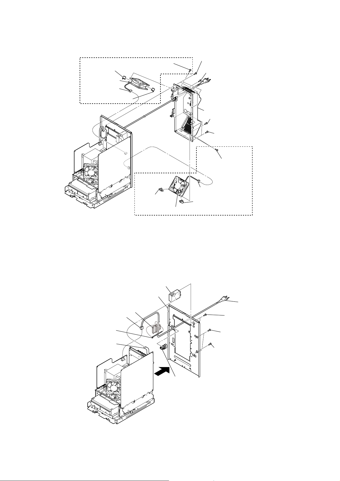
2-7. MAIN BOARD
HCD-GTZ4/GTZ4i/GTZ5
Ver. 1.1
(EXCEPT GTZ4i: US)
7 fan connector
(CN110)
8 connector
(CN907)
qa MAIN board
4 wire (flat type)
(9 core) (CN691)
3 wire (flat type)
(13 core) (CN410)
5 wire (flat type)
(7 core) (CN692)
6 connector
(CN601)
2-8. DC FAN (M102), POWER AMP BOARD
(EXCEPT GTZ4i: US)
1 two screws
(BVTP3 u 8)
4 screw
(BVTP3 u 8)
5 clamp
2 two screws
(BVTP3 u 8)
2 connector
(CN1502)
1 filter clamp
3 bracket (fan)
0 connector
(CN479)
9 two screws
(BVTP3 u 8)
qa heat sink
6 DC fan (M102)
(GTZ4i: US)
7 screw
(BVTT3 u 6)
8 clamp
q; two screws
(transistor)
qs connector
(CN908)
(GTZ4i: US)
qd screw
(BVTP3 u 8)
9 three screws
(BVTP3 u 10)
qd two screws
(BVTP3 u 8)
qf POWER AMP board
7
HCD-GTZ4/GTZ4i/GTZ5
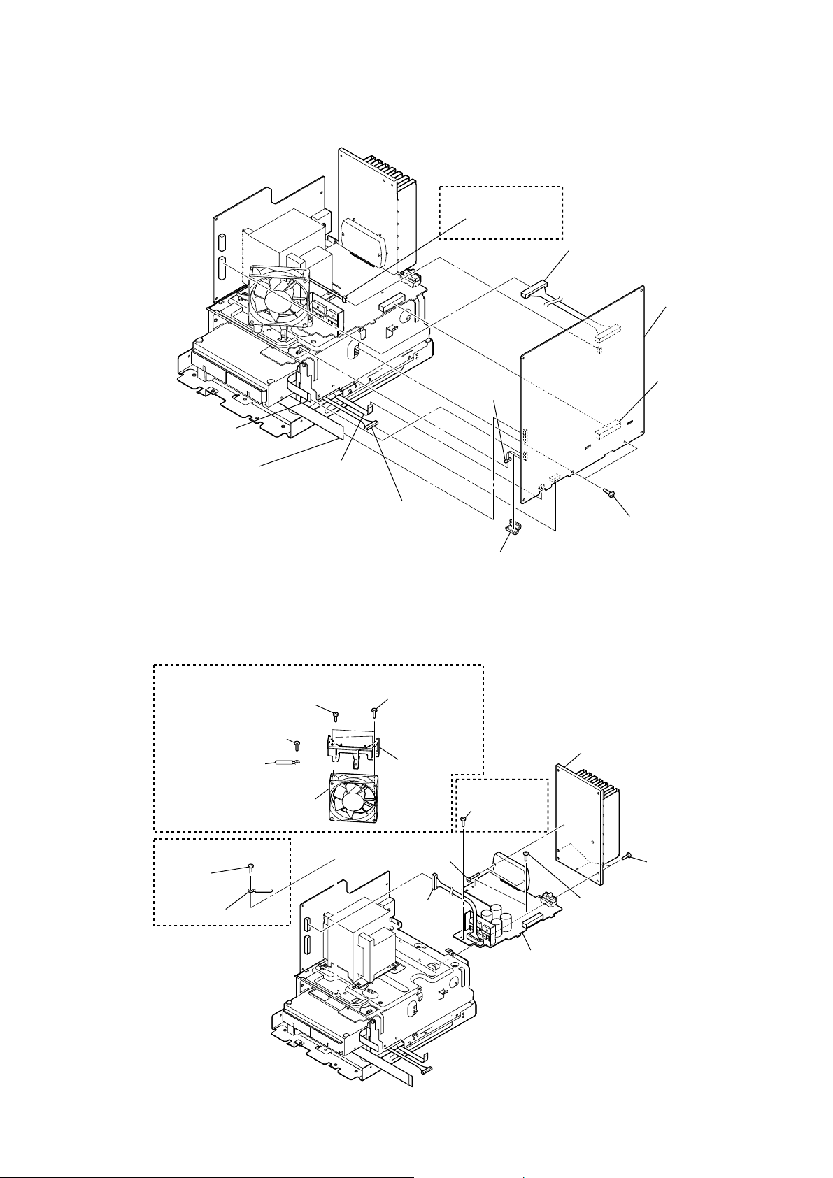
2-9. HUB BOARD, DMB19 BOARD
1 two screws
(BVTP3 u8)
qs two screws
(BVTP3 u8)
6 flat (wire type)
(24 core) (CN101)
4 CD block
0 connector (CN201)
qd bracket
(ground hub)
qa connector
(DMB19 board: CN1105/
HUB board: CN1500)
qf HUB
board
qh DMB19 board
qg four screws
(BVTP3 u8)
2-10. CD MECHANISM BLOCK (CDM88B-DVBU101)
2
9 connector
(DMB19 board: CN601)
8 flat (wire type) (7 core)
(DMB19 board: CN4602)
1 two screws
(BVTP3 u8)
5 chassis block
3 two screws
(BVTP3 u8)
7 flat (wire type) (9 core)
(CN1106)
qa two screws
(BVTP3 u8)
qd CD mechanism block
(CDM88B-DVBU101)
0 three sheets (CDM)
1 flat (wire type) (13 core)
(MOTOR board)
8 cover dust (CDM88-B)
qs cover (CDM88 D-top)
qa screw
(BVTP3 u 8)
4 ferrite core
3 bracket
(MTK)
2 screw
(BVTP3 u8)
7 saranet cushion
9 cover dust (CDM88-A)
7 two saranet cushions
7 saranet cushion
6 bracket (support)
5 two screws (BVTP3 u8)
8
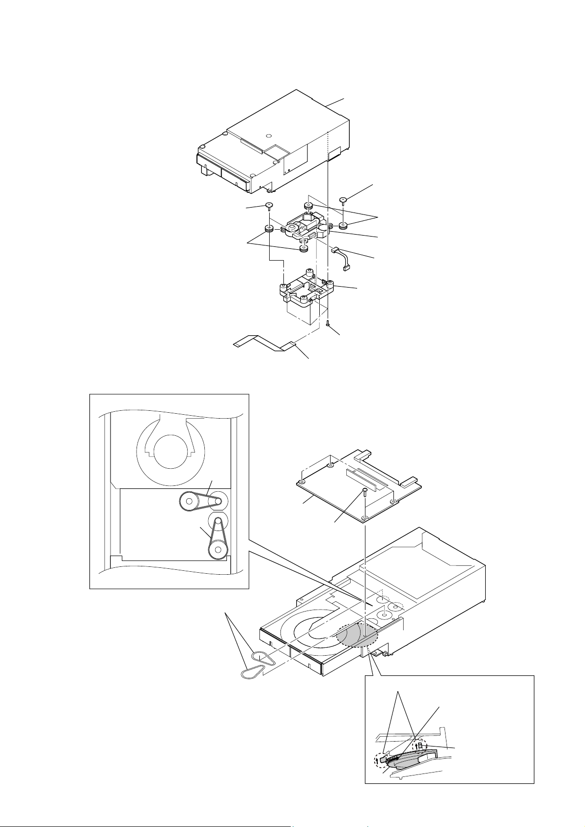
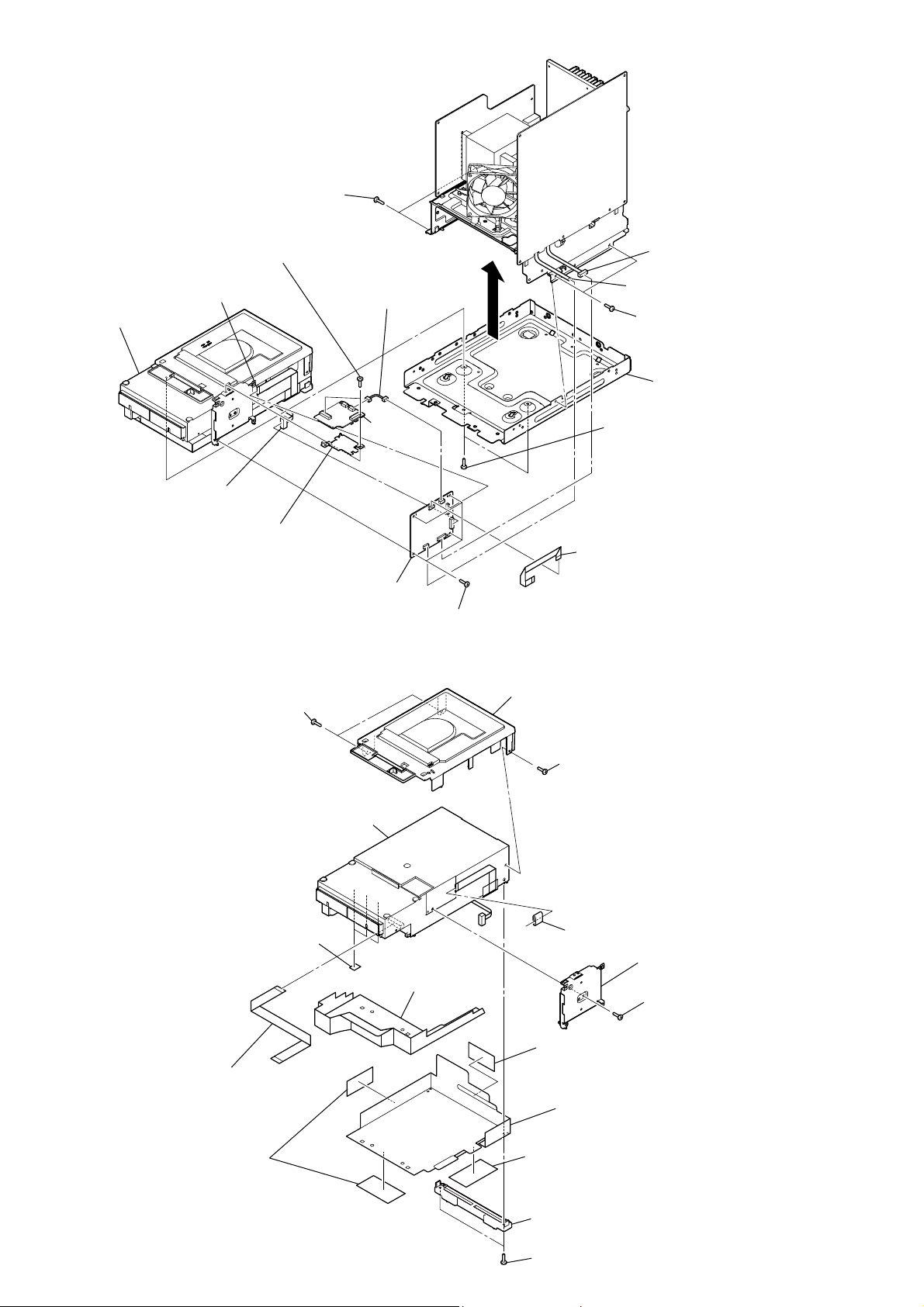
2-11. OPTICAL PICK-UP BLOCK (KHM-313CAB)
HCD-GTZ4/GTZ4i/GTZ5
CD mechanism block
(CDM88B-DVBU101)
4 two insulator screws
2-12. BELT (DLM3A)
position of belt
4 two insulator screws
5 two insulators
belt
5 two insulators
7 optical pick-up block
(KHM-313CAB)
3 connector
6 holder BU
1 four screws
(BVTP2.6)
2 wire (flat type) (24 core)
belt
two belts (DLM3A)
4
3
cover
four screws
2
state of opening the CD tray
1 Turn a gear till a lever
rises up to the position
of the figure.
lever
gear
9

HCD-GTZ4/GTZ4i/GTZ5
SECTION 3
TEST MODE
PANEL TEST MODE
This mode is used to check the fl uorescent indicator tube, LEDs,
keys, [MASTER VOLUME] jog, [OPERATION DIAL] jog, model, destination and software version.
Procedure:
1. Press [x], [METER MODE] and [DISC 2] buttons simultaneously.
2. All LEDs and segments in fl uorescent indicator tube are light-
ed up.
3. When you want to enter to the software version display mode,
press [DISC 1] button. The model information appears on the
fl uorescent indicator tube. “GTL 2S” or “GTL 2SI” is shown
for HCD-GTZ4/GTZ4i, “GTL 3S” is shown for HCD-GTZ5.
Press [DISC 1] button again to view the destination information.
4. During the destination information display, press [DISC 1]
button. Each time [DISC 1] button is pressed, the fl uorescent
indicator tube shows the version of each category software
in the following sequence: SC, MTK (DMB board fi rmware
version), GC, SYS, CD, CDMA, CDMB, ST, TA, TM, MTR
(METER) and return back to model information display.
5. When [DISC 3] button is pressed while the version numbers
are being displayed except model and destination, the date
of the software creation appears. When [DISC 3] button is
pressed again, the display returns to the software version display. When [DISC 1] button is pressed while the date of the
software creation is being displayed, the date of the software
creation is displayed in the same order of software version display.
6. Press [DISC 2] button, the key check mode is activated.
7. In the key check mode, the fl uorescent indicator tube displays
“K 0 J0 V0”.
Each time a button is pressed, “K” value increases. However,
once a button has been pressed, it is no longer taken into account.
“V” value increases in the manner of 0,1, 2, 3 ... if [MASTER
VOLUME] knob is turned clockwise, or it decreases in the
manner of 0, 9, 8,7 ... if [MASTER VOLUME] knob is turned
counterclockwise.
“J” value increases in the manner of 0,1, 2, 3 ... if [OPERA TION
DIAL] knob is turned clockwise, or it decreases in the manner
of 0, 9, 8, 7 ... if [OPERATION DIAL] knob is turned
counterclockwise.
8. When [DISC SKIP/EX-CHANGE] button is pressed after all
LEDs and segments in fl uorescent indicator tube light up, al-
ternate segments in fl uorescent indicator tube and LEDs would
light up. If you press [DISC SKIP/EX-CHANGE] button
again, another half of alternate segments in fl uorescent indi-
cator tube and LEDs would light up. Pressing [DISC SKIP/
EX-CHANGE] button again would cause all segments in fl uo-
rescent indicator tube and LEDs light up.
9. To release from this mode, press three buttons in the same
manner as step 1, or disconnect the power cord.
COMMON TEST MODE
This mode is used to check operations of the respective amplifi er
section.
To enter common test mode
Procedure:
1. Press [x], [METER MODE] and [DISC 3] buttons simultaneously.
2. The CD ring indicators fl ash on the fl uorescent indicator tube.
The function is changed to PC and the volume is changed to
VOLUME MIN.
Check of amplifi er
Procedure:
1. Press [EQ BAND] button repeatedly until a message “GEQ
MAX” appears on the fl uorescent indicator tube. GEQ increas-
es to its maximum.
2. Press [EQ BAND] button repeatedly until a message “GEQ
MIN” appears on the fl uorescent indicator tube. GEQ decreas-
es to its minimum.
3. Press [EQ BAND] button repeatedly until a message “GEQ
FLAT” appears on the fl uorescent indicator tube. GEQ is set to
fl at.
4. When the [MASTER VOLUME] knob is turned clockwise
even slightly, the sound volume increases to its maximum and
a message “VOLUME MAX” appears on the fl uorescent indi-
cator tube.
5. When the [MASTER VOLUME] knob is turned counterclockwise even slightly, the sound volume decreases to its minimum
and a message “VOLUME MIN” appears on the fl uorescent
indicator tube.
To release from common test mode
Procedure:
1. To release from this mode, press [
2. The cold reset is enforced at the same time.
STANDBY] button.
?/1
COLD RESET
The cold reset clears all data including preset data stored in the
EEPROM to initial conditions. Execute this mode when returning
the set to the customer.
Procedure:
1. Press [
2. Press [x], [ENTER] and [
ously.
3. “COLD RESET” appears on the fl uorescent indicator tube.
After that, the fl uorescent indicator tube becomes blank for a
while, and the system is reset.
STANDBY] button to turn on the system.
?/1
ST ANDBY] buttons simultane-
?/1
VACS ON/OFF
This mode is used to switch ON and OFF the VACS (Variable Attenuation Control System).
Procedure:
1. Press [
2. Press [x], [DISC 2] and [DISPLAY] buttons simultaneously.
The message “VACS OFF” or “VACS ON” appears on the
fl uorescent indicator tube.
STANDBY] button to turn on the system.
?/1
10

HCD-GTZ4/GTZ4i/GTZ5
TUNER STEP CHANGE
(Except AEP model)
The step interval of AM channels can be toggled between 9 kHz
and 10 kHz. This mode is not available for AEP model.
Procedure:
1. Press [
2. Press [TUNER/BAND] button repeatedly to select the “AM”.
3. Press [
4. Press [ENTER] and [
ly. The system turns on automatically. The message “AM 9K
STEP” or “AM 10K STEP” appears on the fl uorescent indica-
tor tube and thus the channel step is changed.
STANDBY] button to turn on the system.
?/1
STANDBY] button to turn off the system.
?/1
STANDBY] buttons simultaneous-
?/1
CD SHIP MODE (WITH MEMORY CLEAR)
This mode moves the optical pick-up to the position durable to
vibration and clears all data including preset data stored in the EEPROM to initial conditions during the next AC-In. Use this mode
when returning the set to the customer after repair.
Procedure:
1. Press [
2. Press [CD] button to select CD function.
3. Press [x], [DISC 1] and [
ously. The system turns off automatically.
4. After the “STANDBY” blinking display fi nishes, a message
“MECHA LOCK” is displayed on the fl uorescent indicator
tube and the CD ship mode is set.
5. Unplug the power supply cable.
STANDBY] button to turn on the system.
?/1
STANDBY] buttons simultane-
?/1
CD SHIP MODE (WITHOUT MEMORY CLEAR)
This mode moves the optical pick-up to the position durable to
vibration. Use this mode when returning the set to the customer
after repair.
Procedure:
1. Press [
2. Press [CD] button to select CD function.
3. Press [DISC SKIP/EX-CHANGE] and [
tons simultaneously. The system turns off automatically.
4. After the “STANDBY” blinking display fi nishes, a message
“MECHA LOCK” is displayed on the fl uorescent indicator
tube and the CD ship mode is set.
5. Unplug the power supply cable.
STANDBY] button to turn on the system.
?/1
?/1
STANDBY] but-
CD TRAY LOCK MODE
This mode let you lock the disc tray. When this mode is activated, the disc tray will not open when [Z OPEN/CLOSE] button
or [DISC SKIP/EX-CHANGE] button is pressed. The message
“LOCKED” will be displayed on the fl uorescent indicator tube.
Procedure:
1. Press [
2. Press [CD] button to select CD function.
3. Press [x] and [Z OPEN/CLOSE] buttons simultaneously and
hold down until “LOCKED” or “UNLOCKED” displayed on
the fl uorescent indicator tube (around 5 seconds).
STANDBY] button to turn on the system.
?/1
FACTORY PRESET
This mode is use to load all the factory use preset frequencies
into FM 1-FM 20 and AM 1-AM 10. Originally, frequency of FM
1-FM 20 and AM 1-AM10 are set to the minimum frequency.
Procedure:
1. Press [
2. Press [SURROUND], [x] and [DISC 1] buttons simultaneously and the message “FACTORY” appears on the fl uores-
cent indicator tube. The function is changed to TUNER automatically.
STANDBY] button to turn on the system.
?/1
VACS DISPLAY
This mode is used to check the VACS level.
Procedure:
1. Press [
2. Press [ERASE], [x] and [ENTER] buttons simultaneously.
3. The fl uorescent indicator tube displays “VACSx”. “x” repre-
sents Conventional VACS level (Triggered by signal level).
4. To release from this mode, do the step 2 again.
STANDBY] button to turn on the system.
?/1
METER SWITCH TOUCH COUNT DISPLAY
This mode is used to display the total count of meter pointer touch
initial switch and max switch.
Procedure:
1. Press [
2. Press [x], [ENTER] and [DISPLAY] buttons simultaneously.
3. The fl uorescent indicator tube displays “IxxxxxMyyyyy”.
“I” represents the Initial Switch touch.
“xxxxx” represents the total count of Initial Switch touch.
(Maximum Value of “xxxxx” = 65535)
“M” represents the Max Switch touch.
“yyyyy” represents the total count of Max Switch touch.
(Maximum Value of “yyyyy” = 65535)
4. To release from this mode, do the step 2 again. The fl uorescent
indicator tube displays “MODE OUT”.
STANDBY] button to turn on the system.
?/1
METER TEST MODE
This mode is used to check the meter device.
Procedure:
1. Press [
2. Press [x], [ENTER] and [METER MODE] buttons simultaneously. The fl uorescent indicator tube displays “TST MODE
IN”.
3. Meter Backlight LEDs, Meter Pointer LEDs, Power Illuminator LEDs and fl uorescent indicator tube are lighted up.
4. When you want to perform count total step from Initial Switch
to Max Switch operation mode, press [TUNING + > M]
button. The meter pointer will move from Initial Switch to
Max Switch and fi nally move back to the middle position. The
total step count information appears on the fl uorescent indica-
tor tube. “xxx STP yy” is shown.
“xxx” represents the total step.
(Value of “xxx” should between 430 steps to 470 steps)
“yy” represents the status of total step count.
(If total step between 430 steps to 470 steps, “yy” is OK, Else
“yy” is NG)
5. When you want to perform count total step from Max Switch
to Initial Switch operation mode, press [TUNING – . m]
button. The meter pointer will move from Max Switch to Initial Switch and fi nally move back to the middle position. The
total step count information appears on the fl uorescent indica-
tor tube. “xxx STP yy” is shown.
“xxx” represents the total step.
(Value of “xxx” should between 430 steps to 470 steps)
“yy” represents the status of total step count.
(If total step between 430 steps to 470 steps, “yy” is OK, else
“yy” is NG).
6. To release from this mode, do the step 2 again. The fl uorescent
indicator tube displays “TST MODE OUT”.
STANDBY] button to turn on the system.
?/1
11

HCD-GTZ4/GTZ4i/GTZ5
SECTION 4
ELECTRICAL CHECK
TUNER SECTION
FM TUNE LEVEL CHECK
signal
generator
Procedure:
1. Turn on the set.
2. Input the following signal from signal generator to FM antenna
input directly.
Carrier frequency : A = 87.5 MHz, B = 98 MHz, C = 108 MHz
Deviation : 75 kHz
Modulation : 1 kHz
ANT input : 35 dBu (EMF)
Note: Use 75 ohm coaxial cable to connect signal generator and the set.
You cannot use video cable for checking.
Use signal generator whose output impedance is 75 ohm.
3. Set to FM tuner function and tune A, B and C signals.
4. Confi rm “TUNED” is lit on the display for A, B and C signals.
When the selected station signal is received in good condition,
“TUNED” is displayed.
set
12
HCD-GTZ4/GTZ4i/GTZ5
HCD-GTZ4/GTZ4i/GTZ5
1313
SECTION 5
DIAGRAMS
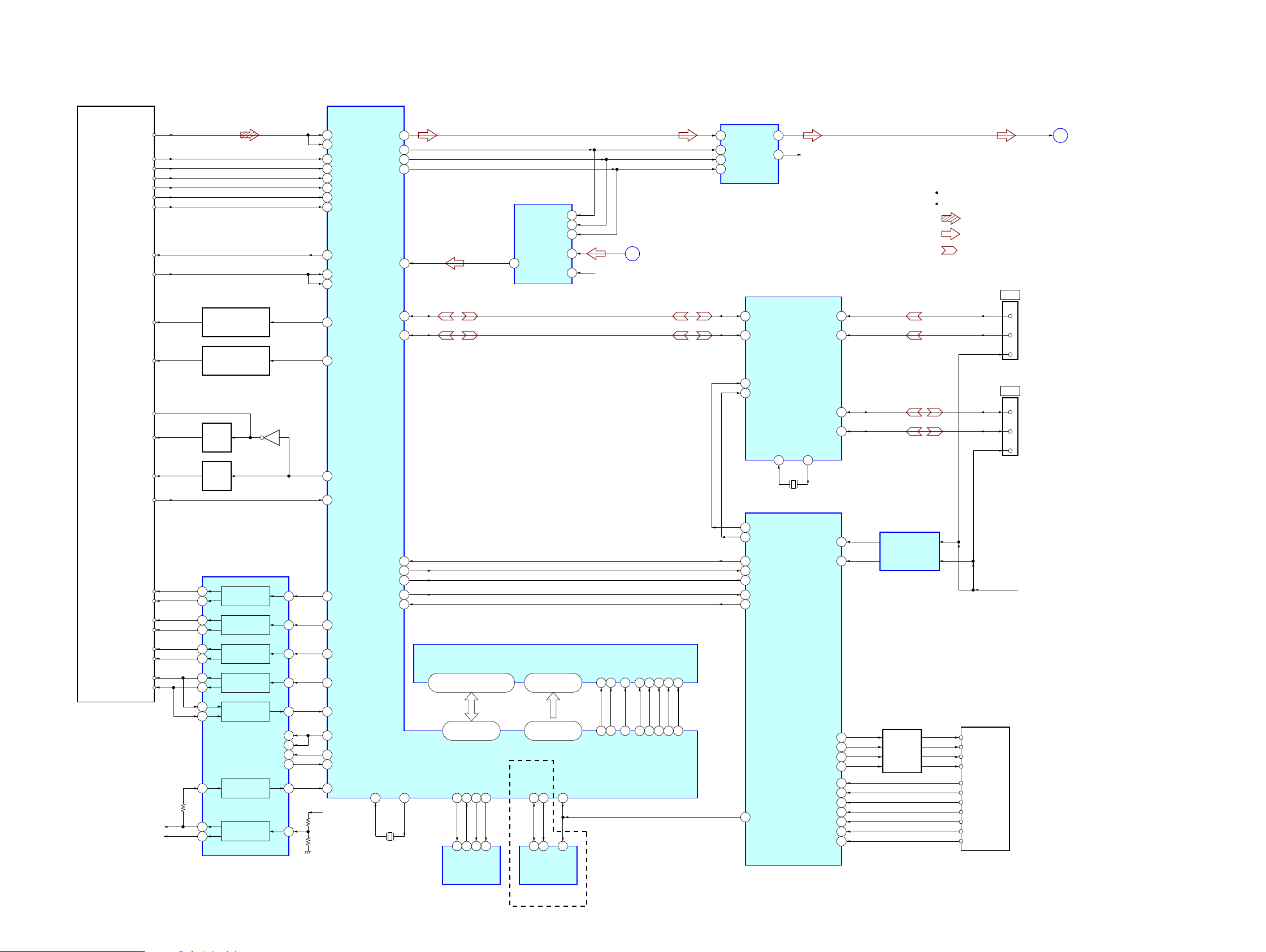
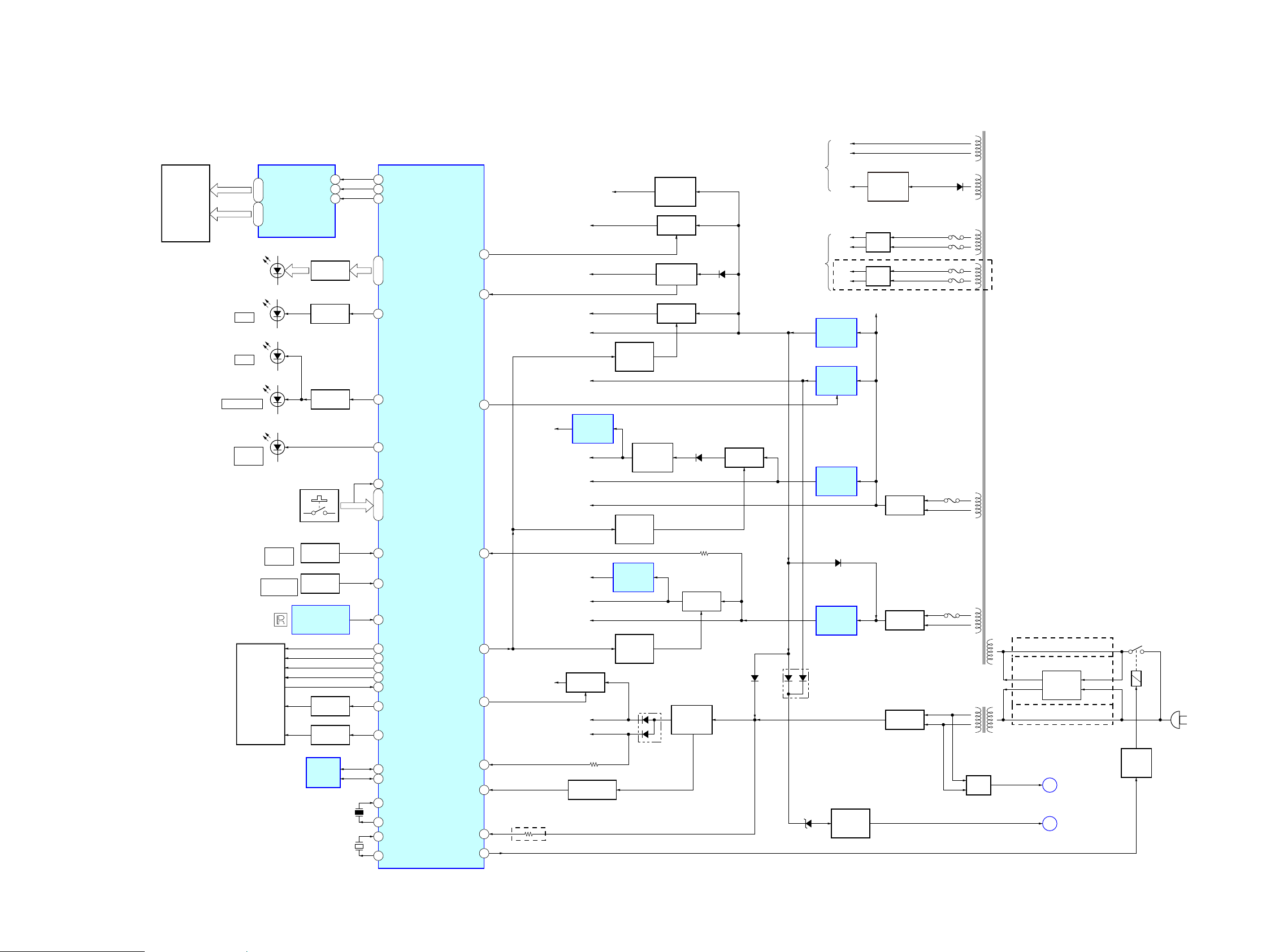
5-1. BLOCK DIAGRAM - RF SERVO, USB Section -
OPTICAL PICK-UP
BLOCK
RF AMP, SERVO DSP,
AUDIO PROCESSOR
IC101
SYSTEM
CONTROLLER
IC401 (1/4)
FOCUS/TRACKING COIL DRIVE,
SPINDLE/SLED MOTOR DRIVE
IC201
AUTOMATIC POWER
CONTROL
Q102-1
RF_IP
125
RF_C
3
RF_B
2
RF_A
1
RF_D
4
RF
VOA/A
VOB/B
VOC/C
VOD/D
RF_F6VOE/E+G
RF_E5VOF/F+H
V2O12VC
LDO117LD (780)
AUTOMATIC POWER
CONTROL
Q102-2
LDO2
18LD (650)
FOO25
CD ON
SWITCH
Q101-1
CD ON
SWITCH
Q101-2
VR (780)
MSW
GPIO
23
118
VR (650)
FCS+
MSW
MDI115
MDI216
PD
LIMIT
Q103
SF_CS#CS_
SD-RAM
IC104
X101
27MHz
36
FCS– 37
1
TRO24
TRK+ 35
TRK– 34
4
FMO21
SL+ 29
SL– 30
10
DMO20
SP+ 27
SP– 28
31
32
41
46
47
13
SPFG/OPINN128
45
GPIO
GPIO
GPIO
120
DG0, DQ1 – DQ15
RD0 – RD15
A0 – A11
RA0 – RA11
2, 4, 5, 7, 8, 10, 11, 13, 42,
44, 45, 47, 48, 50, 51, 53
45 – 49, 51 – 53,
64 – 61, 56 – 59
82, 83, 85, 86,
74 – 69, 81, 67
23 – 26,
29 – 34, 22, 35
36
XTALI
9
1
SF_CKSCK
39
6
BA0 BA0
78
20
BA1 BA1
80
21
RCLK CLK
66
38
DQM0 LDQM
55
15
DQM1 UDQM
65
39
RAS# RAS
77
18
CAS# CAS
76
17
RWE# WE
75
16
: CD PLAY
: AUDIO
: USB
FOCUS
COIL DRIVE
TRACKING
COIL DRIVE
SLED
MOTOR DRIVE
SPINDLE
MOTOR DRIVE
REGULATOR
GPIOMUTE123 116
19
MUTE4MUTE4 22
20
GPIOTSD-M 94
22
IOPMON/
OPINP
127
40
8
PS
21
BUFFER
BUFFER
RF +3.3V
SDAI2C_SDA
34
13
SCLI2C_SCL
33 43
12
PRST#RESET
4
REGO2
REGO1
(KHM-313CAB)
FLASH ROM
IC102
EEPROM
IC106
XTALO
10
A
L-OUT
115
119
GPIO
114
GPIO19
106
VINL
14
13
VINR
BCK
7
LRCK
6
8
SCKI
A/D CONVERTER
IC4601
9
DOUT
B
REC_L
R-CH
USB CONTROLLER
IC13
31
USBUP_DP
30
USBUP_DM
AOUT-L
5
8
AOUT-R
D/A CONVERTER
IC4602
1
SDATA
2
SCLK
3
LRCK
4
MCLK
USB_DP 27
R-CH
USB_DM 28
SO
2SI5
SF_DO37SF_DI
38
(GTZ4i)
CD MECHANISM
DECK
M1M2+
M2-
M1+
M1+
21
M1- 18
M2+
7
M2- 6
MOTOR
DRIVE
Q640, 641,
Q643 - 648
SW3
SW2
SW7-CHACK
SW1
SW1
23
SW3
22
SW2
25
SW-CHUCK
24
SW5-STOCK
SW8-OPEN
SW6-CLOSE
SW-STOCK
27
SW-CLOSE
26
SW-OPEN 28
2USBDN1_DP
1USBDN1_DM
73MTK-OC2
CN1001
(USB)
3
2
1
D+
D–
68MTK-OC1
VBUS
VBUS OVER
CURRENT DETECT
IC1500
4USBDN2_DP
3USBDN2_DM
3
2
1
D+
D–
VBUS
MTK-RST48
MTK-TX
35
MTK-RX
36
MTK-CLOCK
37
MTK-XIFCS
34
MTK-BUSY
19
IFSDI 35
IFSOD
41
IFSCK
40
IFCS#
88
IFBSY
87
VBus_Det57
HUB_RST
47
VBUS_DET27
RESET_N
26
X1500
24MHz
XTAL1/
CLKIN
33
XTAL2
32
USB +5V
USB A
CN1000
(USB)
USB B
SIGNAL PATH
R-ch is omitted due to same as L-ch.
OPOUT126
(Page 14)
(Page 14)
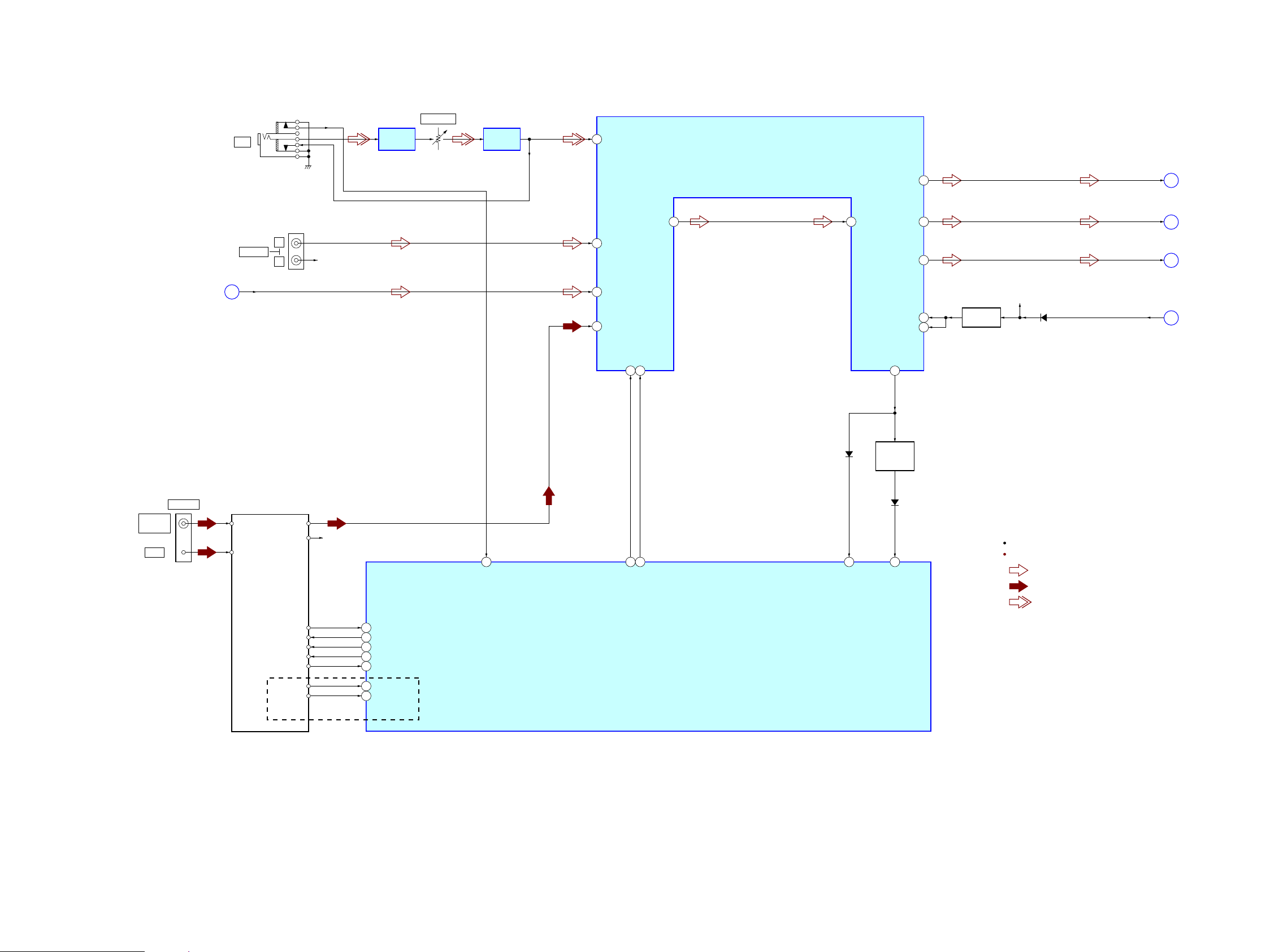
HCD-GTZ4/GTZ4i/GTZ5
HCD-GTZ4/GTZ4i/GTZ5
1414
5-2. BLOCK DIAGRAM - MAIN Section -
R-CH
TUNER (FM/AM)
AM
FM ANT
AM ANT
ST-L
ST-R
ST-DOUT
R-CH
ST-DIN
ST-CLK
ST-CE
FM75:
COAXIAL
ANTENNA
TUNED
61 ST-TUNED
RDS-DATA
76 ST-RDS-DATA
RDS-INT
75 ST-RDS-INT
43 ST-L
21
DATA22CLK
4230AUX-L
46 MIC
29 VOLINLTONEOUTL 26OUTL
44 CD-L
67 ST-DOUT
66 ST-CLK
63 ST-CE
R2A15216FP-DATA
60
9
SA2
POWER ILLUMINATOR
71
VACS IN
89
R2A15216FP-CLK
59
MIC DET
45
23SWOUT
28BB1L
37RECAL
BAND-PASS
FILTER
Q115
R-CH
27BB2L
BASS AGC
Q128
D630
D201
INPUT SELECTOR,
ELECTRICAL VOLUME
IC407
SYSTEM CONTROLLER
IC401 (2/4)
: AUDIO
SIGNAL PATH
R-ch is omitted due to same as L-ch.
: TUNER (FM/AM)
(GTZ4i: AEP)
J700
MIC
RV700
MIC LEVEL
MIC AMP
IC700 (1/2)
MIC AMP
IC700 (2/2)
E
F
D
65 ST-DIN
R
LJ120
PC IN
A
L-OUT
D116
REC-L
B
OUT
SW OUT
BASS AGC
: MIC
(Page 13)
(Page 13)
(Page 15)
(Page 15)
(Page 15)
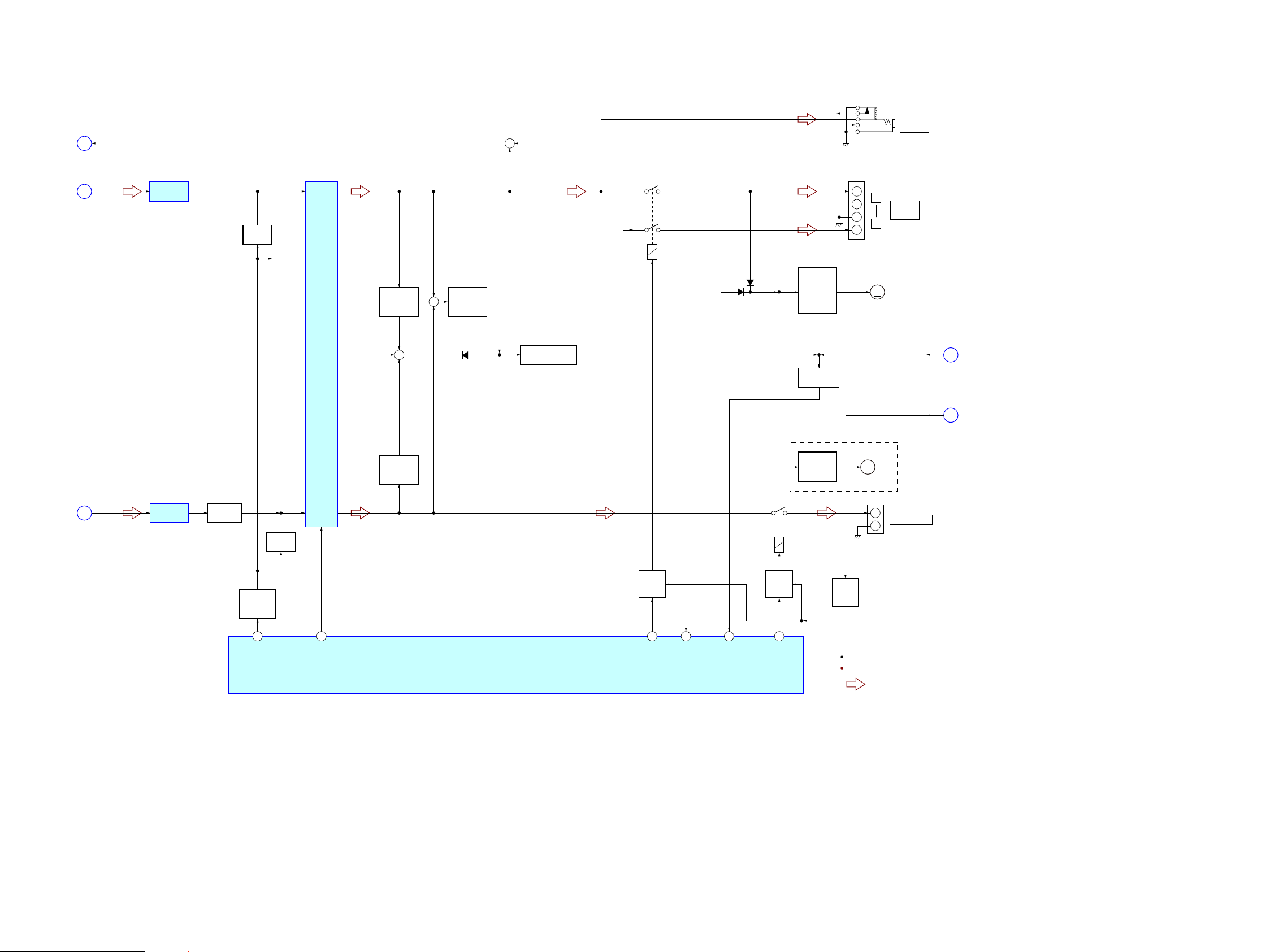
HCD-GTZ4/GTZ4i/GTZ5
HCD-GTZ4/GTZ4i/GTZ5
1515
5-3. BLOCK DIAGRAM - AMP Section -
LINE AMP
IC252
D
F
E
POWER
AMP
IC800
MUTING
Q402
OVER LOAD
DETECT
Q801
OVER LOAD
DETECT
Q802
R-CH
MUTING
Q430
LINE AMP
IC253
+
R-CH
R-CH
R-CH
–1
–2
MUTING
CONTROL
Q670
LINE MUTE
58
STK MUTE
51
SW SPK RELAY
52
+
R-CH
FAN MOTOR
DRIVE
Q693 – 695,
Q697
RY800
+
–
–
+
RY500
D632
D807
M
M101
(FAN)
FAN MOTOR
DRIVE
Q110 - 113
M
M102
(FAN)
PHONES
+
–
SUBWOOFER
JK500
RELAY
DRIVE
Q500
FR SPK RELAY
53
PROTECT
50
RELAY
DRIVE
Q804
R-CH
J702
SYSTEM CONTROLLER
IC401 (3/4)
: AUDIO
SIGNAL PATH
R-ch is omitted due to same as L-ch.
+
OVER LOAD
DETECT
Q803
R
L
FRONT
SPEAKER
JK800
G
H
LEVEL SHIFT
Q447
BASS AGC
OUT
SW OUT
BUFFER
Q431
AC CUT
DETECT
Q501
PROTECT DETECT
Q806 – 809, 811
HP_DET
44
DC DETECT
PROTECT
(GTZ4/GTZ4i: AEP, Australian/GTZ5)
(Page 14)
(Page 14)
(Page 14)
(Page 16)
(Page 16)
Ver. 1.1
HCD-GTZ4/GTZ4i/GTZ5
HCD-GTZ4/GTZ4i/GTZ5
1616
5-4. BLOCK DIAGRAM - PANEL, POWER SUPPLY Section -
REMOTE CONTROL
RECEIVER
IC1100
FL1100
FLUORESCENT
INDICATOR
TUBE
3 SW/USB CTRL
AD-KEY0 –
AD-KEY2
FLUORESCENT INDICATOR
TUBE DRIVER
IC1101
SYSTEM CONTROLLER
IC401 (4/4)
F907
RECT
D911, 912
PROTECT
DETECT
Q606
RECT
D610 – 613
LED-VOL1. 2 –
LED-VOL5. 6
S1100 – 1119,
S1121, 1123,
S1122,
S1124 – 1132
54STBY RELAY
20AC-CUT
RESET SWITCH
Q210, 214, 215
D213
+3.3V
UNREG +16V
83OVERVOLTAGE
12RESET
91 MASTER VOL
SG5/KS5 –
SG24/KS24
14 – 33
79 – 7797, 95, 94
D1105 – 1110
(STREAM)
LED DRIVE
Q1122
70 USB-LED CTRL
LED DRIVE
Q1121
D1104
SUBWOOFER
72 STBY LED
AD KEY0
4 SIRCS
D1011
I/1
STANDBY
ROTARY
ENCODER
MASTER
VOLUME
OPERATION
DIAL
S1301
90 OPERATION DIAL
ROTARY
ENCODER
S1300
13 X-OUT
15 X-IN
X402
5MHz
11 XC-OUT
10 XC-IN
X401
32.768kHz
DIN
FL-DRIVER-DATA2 86
CLK
FL-DRIVER-CLK1 85
EEP-SDA55
EEP-SCL56
STB
FL-DRIVER-CS3 87
74 POWER/DISPLAY-KEY
(AC IN)
RY901
RELAY
DRIVE
Q903
VOLTAGE
SELECTOR
S901
DVDD +3.3V
D607D628
D623, 624
FAN B+
D908
TUNER +9V,
A+9V
A+9V
F906
RECT
D601
F904
F905
F908
F909
RECT
D800
D608
+9V
REGULATOR
IC678
+9V
REGULATOR
IC602
AVDD +5V
+5V
REGULATOR
Q696
VM+9V
+3.3V
REGULATOR
IC603
+4V
REGULATOR
Q211, 212
LED SEL A,
LED SEL B
CD MECHANISM
MOTOR B+
REGULATOR
Q655 – 658
69LED CTRL
5CDM-SD
JOG B+
43AD SUPPLY SW
B+ SWITCH
Q627, 628
–32V
REGULATOR
Q902
AMP
SECTION
B+
FOR
FLUORESCENT
INDICATOR
TUBE
(GTZ4i: US/GTZ5)
–VFL
VF
VF
PT902
SUB POWER
TRANSFORMER
PT901
MAIN POWER
TRANSFORMER
(GTZ4: AR/GTZ4i/GTZ5: MX, AR)
(GTZ4: E2, E51/GTZ5: E2, E51)
VCC +3.3V
EVER +3.3V
+VH
–VH
Abbreviation
AR : Argentina model
E2 : 120V AC area in E model
E51 : Chilean and Peruvian models
MX : Mexican model
D1002, 1003
EEPROM
IC675
(GTZ4: AR/GTZ4i/GTZ5: MX, AR)
PROTECT
G
DC DETECT
GR1 – GR14
34 – 47
LED DRIVE
Q1118 – 1120
USB B
D1000
USB A
(GTZ4: E2, E51/GTZ5: E2, E51)
B+ SWITCH
Q676
AVDD +1.8V
82
MTK POWER
MONITOR
42MTK PWR CTL
B+ SWITCH
Q675
RF +3.3V
+5V
REGULATOR
IC677
46MTK OE
USB +5V
B+ SWITCH
Q677
D651
B+ SWITCH
Q1114 – 1117
39
METER LED
CTRL
METER
DISPLAY
BLOCK
H
RECT
D1210
+1.8V
REGULATOR
IC111
POWER
CONTROL
Q674
POWER
CONTROL
Q673
+3.3V
REGULATOR
IC107
POWER
CONTROL
Q672
D700 – 702
31 METER BL CTL
LED DRIVE
Q231
LED DRIVE
Q230
81 METER SW
2 METER-IN4
1 METER-IN3
84 METER-IN2
METER-IN1100
+5V
REGULATOR
Q698
M+5V
RECT
D801
+VH
–VH
(Page 15)
(Page 15)
Ver. 1.1
HCD-GTZ4/GTZ4i/GTZ5
HCD-GTZ4/GTZ4i/GTZ5
1717
• Circuit Boards Location
For Schematic Diagrams.
Note:
• All capacitors are in μF unless otherwise noted. (p: pF) 50
WV or less are not indicated except for electrolytics and
tantalums.
• All resistors are in Ω and 1/4 W or less unless otherwise
specifi ed.
• f : Internal component.
• 2 : Nonfl ammable resistor.
• 5 : Fusible resistor.
• C : Panel designation.
THIS NOTE IS COMMON FOR PRINTED WIRING BOARDS AND SCHEMATIC DIAGRAMS.
(In addition to this, the necessary note is printed in each block.)
• A : B+ Line.
• B : B– Line.
• Voltages and waveforms are dc with respect to ground
under no-signal (detuned) conditions.
no mark : TUNER (FM/AM)
( ) : CD PLAY
< > : USB
{ } : PC
* : Impossible to measure
• Voltages are taken with VOM (Input impedance 10 MΩ).
Voltage variations may be noted due to normal production
tolerances.
• Waveforms are taken with a oscilloscope.
Voltage variations may be noted due to normal production
tolerances.
• Circled numbers refer to waveforms.
• Signal path.
F : AUDIO
J : CD PLAY
f : TUNER (FM/AM)
L : MIC
E : USB
• Abbreviation
AR : Argentine model
AUS : Australian model
E2 : 120V AC area in E model
E51 : Chilean and Peruvian models
MX : Mexican model
For Printed Wiring Boards.
Note:
• X : Parts extracted from the component side.
• Y : Parts extracted from the conductor side.
• f : Internal component.
• : Pattern from the side which enables seeing.
(The other layers’ patterns are not indicated.)
• Indication of transistor.
CEB
These are omitted.
Caution:
Pattern face side:
(SIDE B)
Parts face side:
(SIDE A)
Parts on the pattern face side seen
from the pattern face are indicated.
Parts on the parts face side seen from
the parts face are indicated.
Note: The components identifi ed by mark 0 or dotted
line with mark 0 are critical for safety.
Replace only with part number specifi ed.
Caution:
Pattern face side:
(Conductor Side)
Parts face side:
(Component Side)
Parts on the pattern face side seen
from the pattern face are indicated.
Parts on the parts face side seen from
the parts face are indicated.
• Abbreviation
AR : Argentine model
AUS : Australian model
E2 : 120V AC area in E model
E51 : Chilean and Peruvian models
MX : Mexican model
• DMB19 board is multi-layer printed board.
However, the patterns of intermediate layers have not
been included in diagrams.
d
Ver. 1.1
C
Q
B
E
These are omitted.
TRANS board
MOTOR DRIVE board
LED board
MAIN board
POWER AMP boar
DMB19 board
HUB board
TUNER (FM/AM)
SW board
VOLUME board
HEADPHONE board
USB board
MIC board
DISPLAY board
HCD-GTZ4/GTZ4i/GTZ5
HCD-GTZ4/GTZ4i/GTZ5
1818
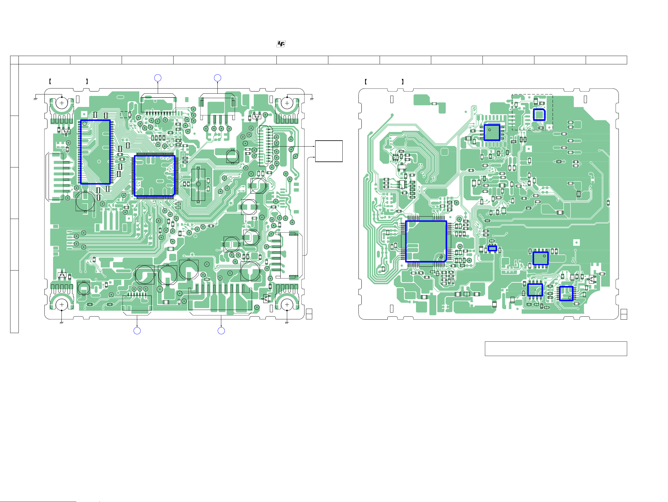
5-5. PRINTED WIRING BOARD - DMB19 Board -
Note: When IC102 cannot exchange with single. When this part
is damaged, exchange the entire mounted board.
1
7
1
9
1
9
C1504
R605
CN201
R1110
CN4602
R230
R1114
R231
R232
CN601
R1121
R1123
C4608
R246
R247
JL001
JL002
JL003
JL004
JL005
JL006
C216
JL007
C217
C218
CL105
CL106
C602
CL107
C603
CL108
C604
CL109
JL201
JL202
JL203
JL010
C220
C608
JL205
JL012
JL206
JL014
R4601
JL016
JL017
C611
JL210
JL211
JL212
JL213
JL214
JL215
R1151
R1152
C620
C622
C623
FB1264
FB1265
FB1266
R1168
D001
D002
C621
D003
D004
R4837
R4838
RB105
ET001
RB106
ET002
RB107
ET003
RB108
ET004
RB111
RB112
RB113
RB114
RB115
JL1201
JL1202
JL1203
JL1204
JL1205
JL1206
JL1207
JL1208
JL1209
JL1210
JL1211
JL1212
JL1213
JL1214
JL1216
JL1218
JL1220
R102
R103
R107
R114
CN101
CN105
C101
C103
C105
R142
C106
X101
C112
C113
C118
R156
C124
CL206
CL207
CL208
JL113
JL114
JL115
CL213
R1248
R1249
R1263
C152
C153
R1269
R1270
R1271
C160
R1276
R1277
R1281
R1282
R1283
IC101
IC104
JL1101
JL1102
JL1105
JL1106
JL1107
JL1108
C190
JL1110
JL1111
JL1112
JL1113
JL1114
JL1115
JL1116
JL1117
CL1138
JL1118
CL1139
JL1119
CL1140
JL1120
CL1141
JL1121
CL1142
JL1122
JL1123
JL1124
CL1146
CL1147
CL1148
CL1149
CN1105
CN1106
CL1150
CL1151
JL1131
CL1152
JL1132 JL1133
JL1134
1
12
13
48
24
25
36
37
IO
C1
E1
B1
B2
E2
C2
D1
G2
S2
G1
D2
S1
FB607
R210
C1505
R212
C1506
R213
C1507
R214
R215
R216
R219
R1101
C1512
R606
C1513
R220
R608
R221
R223
R224
R225
R226
R233
R234
C4602
C4603
C4606
C203
C205
C206
C208
R1129
C209
R630
C210
C211
C212
C213
C214
C215
C219
R256
C4622
C4623
C221
C4626
C222
C224
R4602 R4605
R4606
R4608
R4609
IC4601
IC4602
R1150
C233
R4611
FB1267
FB1268
R1177
R1178
D005
Q101
Q102
Q103
R4833
R1184
R4834
R4835
R1191
R1192
R1193
R1194
IC201
FB108
R101
R104
R105
R108
R109
R110
R111
R112
R113
R115
R116
R117
R118
R120
R121
R122
R123
R124
R125
R133
R136
R521
C102
C104
C108
C111
C115
C116
C119
C502
CL201
CL202
CL204
C125
CL205
C126
C127
R1250
R1252
R1254
R1255
R1256
C144
C145
C146
C149
R1261
R1262
C150
C151
C154
C155
C156
R1278
R1279
C168
C169
R1280
C172
C175
C179
C180
C181
IC102
C183
IC106
IC107
C188
C191
IC111
C192
C193
C195
C197
C198
C199
FL603
R204
R205
R206
R207
R208
R209
FB603
A
B
C
D
E
1 2 3 4 5 6 7 8 9 10 11 12
1
32
1
6
1
27
54
28
96
97 128
64
33
65
6
1
23
1
24
2
4
1
D
MAIN BOARD
CN692
C
MAIN BOARD
CN601
A
HUB BOARD
CN1500
B
MAIN BOARD
CN691
K
A/K
A
K
A/K
A
K
A/K
A
1-878-221-
12
(12)
DMB19 BOARD (SIDE A)
K
A/K
A
OPTICAL
PICK-UP
BLOCK
(KHM-313CAB)
(NC)
(CHASSIS)
(CHASSIS)
(CHASSIS)(CHASSIS)
(GTZ4i)
(GTZ2i/GTZ3i)
1-878-221-
12
(12)
DMB19 BOARD (SIDE B)
13
45
18
15
6
10
20
16
1511
45
1
14
7
8
1
8
4
5
184
5
K
A/K
A
(GTZ4i)
E
(Page 22) (Page 26)
(Page 22) (Page 22)
• : Uses unleaded solder.
• See page 17 for Circuit Boards Location.
HCD-GTZ4/GTZ4i/GTZ5
HCD-GTZ4/GTZ4i/GTZ5
1919
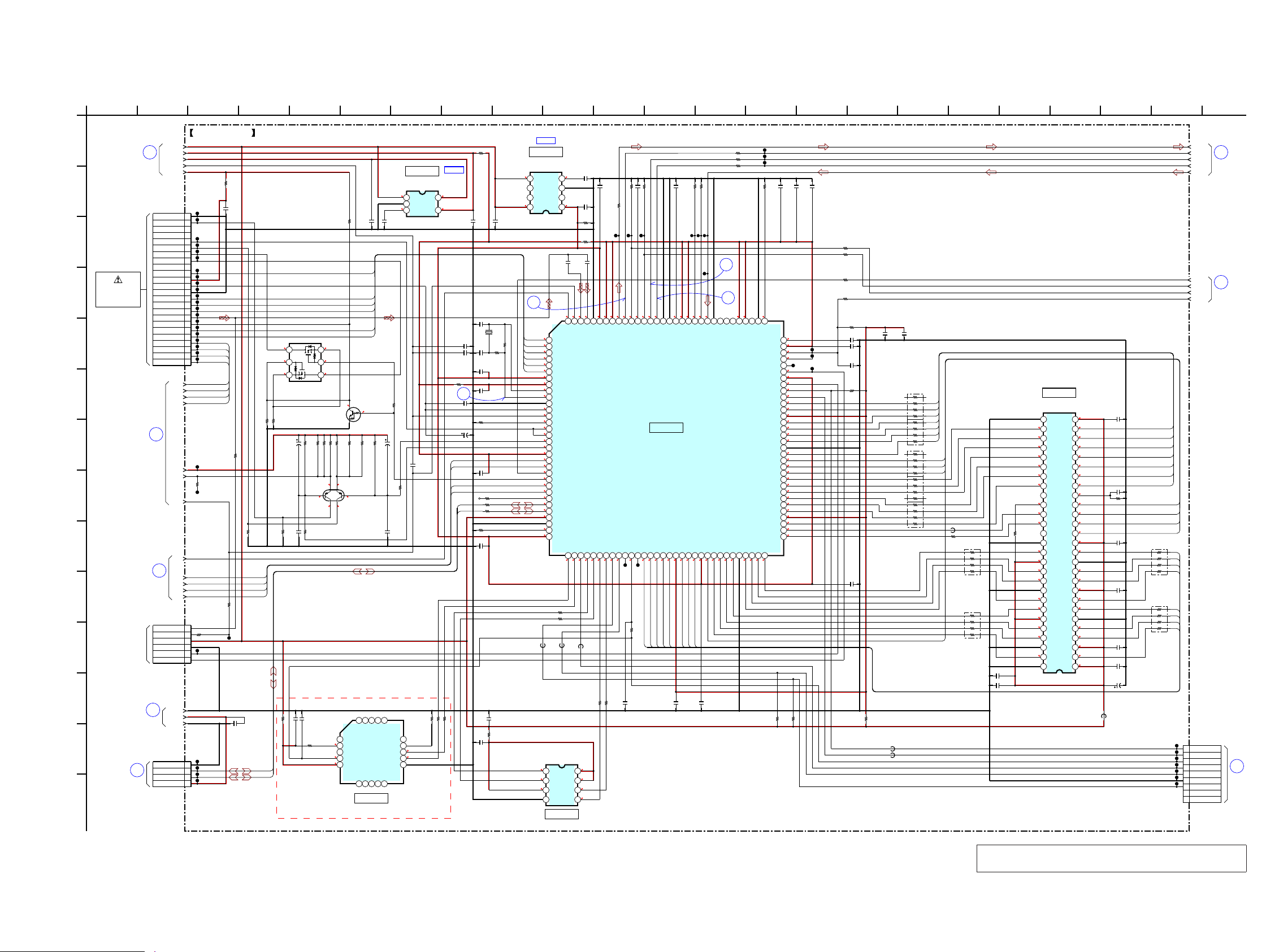
• See page 36 for Waveforms. • See page 36 for IC Block Diagrams. • See page 39 for IC Pin Function Description.
5-6. SCHEMATIC DIAGRAM - DMB19 Board (1/3) -
Note: When IC102 cannot exchange with single. When this part
is damaged, exchange the entire mounted board.
(2/3)
MAIN
BOARD
B
CN691CN1500
HUB
BOARD
A
BOARD
(2/3)
6
DMB19
5
(3/3)
DMB19
BOARD
(2/3)
BOARD
DMB19
1
IC B/D
IC B/D
4
(3/3)
DMB19
BOARD
(2/3)
DMB19
3
BOARD
(2/3)
DMB19
2
BOARD
1
2
3
4
0.4 (0.1) 0.4 (2)
3.7 (3.2)3.7
3.3 (2.6)3.3
0.1
5
0.1
0.1
0.1
0.1
5
0.1
3.3
1.3
5
3.3
3.3
3.3
0.6
1.8
3.3
3.3
3.3
3.3
0.1
0.4
1.3
3.3
3.3
1
0.2
3.3
1.5
1.5
1.4
1.5 (1.1)
0.1
0.1
0.1
3.1
1.6
2
3.3
2
1.5
1.3 (2.2)
1.3 (2.2)
0.6
0.1
1.2
0
3
2.8
3.1
2
3.3
1.3 ()
0.5 ()
0.6 ()
0.9 ()
1.3 ()
1 ()
1 ()
3.3
3.3
3.3
1.4 ()
1.5 ()
3.3
3.3
1.8 ()
1.1 ()
1.3 ()
2 ()
1.5 ()
1.9 ()
0.6 ()
0
3.3
3.1
0.1
3.3
3.3
1.8
3
2.5
1.5
1.3 (2.2)
1.3 (2.2)
3.3
0.6
0.1
2
1.2
3
2.8
3.1
1.5
1.5
1.4
1.5 (1.1)
0.1
0.1
0.1
3.3
1.6
2
1.3
3.3
3.3
1.2
0.1
0.1
3.3
3.3
1
1.7
3.3
1.7
1.6
0.1
1.713.3
3.3
1.8
1.1
1.1
1.5
2.7
2
2
2
2
2
2
1.8
3.3
0.9
0.6
2
1.5
0.7
0.1
0.1
3.3 (2.6)
3.3
3.3
1.5
1.5
3.3
0.1
1.5
1.5
3.3
2.9
0.1
3.3
0.8
1.8
0.1
3.313.3
0.4
1.3
0.2
3.1
0.1
3.3
1.4 ()
1 ()
1 ()
1.3 ()
0.9 ()
3.3
0.6 ()
0.5 ()
1.3 ()
1.8
2
0.6 ()
1.9 ()
1.5 ()
2 ()
1.3 ()
1.1 ()
1.8 ()
1.5 ()
1
2
3
4
5
6
6P
CN105
TXD
RXD
GND
+3.3V
V2REFO
RFMON
47k
R124
3.3k
R1151
0.01
C192
0.1
C179
100
R156
22
R112
2.7kR1110
100k
R114
0.1
C116
100
R109
0.01
C113
22R115
100
R101
10k
R107
10V
47
C105
0.22
C195
47k
R117
1k
R116
1
C124
3.3k
R1150
0.01
C101
22
R121
0.1C115
10V
47
C112
1M
R108
1
2
3
4
5
6
7
8
9
10
11
12
13
14
15
16
17
18
19
20
21
22
23
24
CN101
24P
GND (LD)
LD (650)
NC
NC
PD
LD (780)
VR (650)
VR (780)
NC
VOE/E+G
VCC
VC
GND (PDIC)
VOF/F+H
VOB/B
VOA/A
RF
(LO:DVD.HI:CD)MSW
VOD/D
VOC/C
TRKTRK+
FCS+
FCS-
0.01
C106
3.3k
R1152
22R113
100
R123
10V
100
C190
47kR110
0.22
C193
22R118
RT1N241C-TP-1
Q103
0.01
C160
22
R120
0.1
C191
100k
R1129
15k
R136
100
R111
0.1
C197
0.01
C144
0.1
C180
C169
0.1
D1
G2
S2
D2
G1
S1
UM6K1N-TN
Q101
Q102
QST8TR
JL1101
JL1102
JL1105
JL1106
JL1107
JL1108
JL1110
JL1111
JL1112
JL1113
JL1114
JL1115
JL1116
JL1117
JL1118
JL1119
JL1120
JL1121
JL1122
JL1123
JL1124
JL1207
JL1205
JL1204
JL1203
JL1202
JL1201
CL106
CL107
REG01
TRK-
TRK+
FCS+
FCS-
REG02
TRO
IOP
FOO
IOPMON
SPFG
TSD_M
DMO
ALRCK
FMO
ABCK
ACLKVREFO
ASDATA0
RF+3.3V
DVDD5V
DVDD3.3V
C188
470p
1
C198
1
C183
1k
R1178
DGND
FB108
0.1
C181
LIMITSW
R1114
0R133
MUTE4
MUTE123
ADIN
CL1141
100R1184
560
R1101
R102
0
27MHz
X101
8
7
6
54
3
2
1
MX25L1605DM2I-12G
IC102
_CS
SO
_W
GND SI
SCK
_HOLD
VCC
USB+5V
JL1133
JL1132
JL1134
JL1131
220p
C1504
JL113
JL114
JL115
CL105
1
C127
1
2
3
4
5
6
7
8
9
10
11
12
13
14
15
16
17
18
19
20
21
22
23
24
25
26
27
28
29
30
31
32
33 34 35 36 37 38 39 40 41 42 43 44 45 46 47 48 49 50 51 52 53 54 55 56 57 58 59 60 61 62 63 64
65
66
67
68
69
70
71
72
73
74
75
76
77
78
79
80
81
82
83
84
85
86
87
88
89
90
91
92
93
94
95
96
979899
100101102103104105106107108109
110
111
112113114115116117118119
120121122123124
125126127128
CXD9968R
IC101
RF_A
RF_B
RF_C
RF_D
RF_E
RF_F
AVDD18_2
AVDD33_1
XTALI
XTALO
AGND33
V20
V14/VREF0
REXT
MDI1
MDI2
LDO1
LDO2
AVDD33_2
DMO
FMO
MUTE4
MSW
TRO
FOO
EEWP
USB_DP
USB_DM
VDD33_USB
VSS33_USB
PAD_VRT
VDD18_USB
SCL
SDA
IFSDI
SF_CS#
SF_DO
SF_DI
SF_CK
IFSCK
IFSOD
ICE
PRST#IRRD0
RD1
RD2
RD3
RD4
DVDD33
RD5
RD6
RD7
DVDD18
DQM0
RD15
RD14
RD13
RD12
DVSS33
RD11
RD10
RD9
RD8
DQM1
RCLK
RA11
DVDD33
RA9
RA8
RA7
RA6
RA5
RA4
RWE#
CAS#
RAS#
BA0
DVSS18
BA1
RA10
RA0
RA1
DVDD33
RA2
RA3
IFBSY
IFCS#
RX
DVDD18
TX
XMAMUTE
SPDIF
GPIO
DACVDDC
VREF
FS
DACVSSC
CVBS
DACVDDB
DACVDDA
SY/Y/G
SC/CB/B
CR/R
AADVSS
GPIO19
MUTE123
LIMITSW
AADVDD
APLLVDD
APLLCAP
ADACVSS2
ADACVSS1
GPIO
GPIO
GPIO
AVCM
GPIO
GPIO
GPIO
ADACVDD1
ADACVDD2
AVDD18_1
AGND18
RFIP
OPOUT
IOPMON/OPINP
SPFG/OPINN
CL108
CL109
10k
R125
0.01
C1505
0.01
C156
0.01
C151
0.01
C175
0.01
C172
1
C146
0.01
C145
0.1
C154
CL1142
CL1146
CL1147
CL1140
0.1
C102
16V
10
C118
10
C119
0
RB106
0
RB105
1
2
3
4
5
6789
10
11
12
13
14
15
1617181920
MFI341S2161
IC106
NC
MODE1
NC
RESET
VCC
NCNCNCNCNC
VSS
I2C_SCL
I2C_SDA
MODE0
NC
NCNCNCNCNC
0.1
C103
0.01
C104
47
48
49
8
50
51
52
53
54
1
2
3
4
5
6
7
41
42
43
44
45
46
14
13
12
11
10
9
34
40
35
36
37
38
39 16
15
17
18
19
20
21
28 27
29
30
31
32
33
26
25
24
23
22
EM638165TS-6G
IC104
VDD
DG0
VDDQ
DQ1
DQ2
VSSQ
DQ3
DQ4
VDDQ
DQ5
DQ6
VSSQ
DQ7
VDD
LDQM
WE
CAS
RAS
CS
BA0
BA1
A10/AP
A0
A1
A2
A3
VDDVSS
A4
A5
A6
A7
A8
A9
A11
NC
CLKE
CLK
UDQM
NC
VSS
DQ8
VDDQ
DQ9
DQ10
VSSQ
DQ11
DQ12
VDDQ
DQ13
DQ14
VSSQ
DQ15
VSS
0
RB108
0
RB107
0RB111
0
R104
0
R105
CL1138
CL1139
1500p
C108
10C126
8
7
6
54
3
2
1
MM1661JHBE
IC111
Vo
NC
GND
CnCont
NC
NC
Vin
USBGND
1
2
3
4
4P
CN1105
USBGND
USBP
USBM
USB+5V
CL1148
CL1149
CL1150
CL1151
RB112 0
0
RB114
0RB115
0RB113
JL1206
1
2
3
4
5
6
7
8
9
9P
CN1106
XIFCS
XIBSY
XSYSRST
IFSDI
IFSOD
DGND
IFSCK
NC
NC
CL1152
0.1
C1513
0R1263
0
R1250
0.01
C149
C168
0.1
R1249
1k
0.01
C150
0.1
C1512
10k
R122
10kR1262
10kR1261
100
R1269
1000p
C1506
0R1194
0
R1191
R1271 0
R1270
0
0
R1193
0.1C125
0.1
C155
12p
C153
12p
C152
100k
R142
330
R1168
0R1121
5.1kR103
0R1123
0R1177
0.1
C111
0R1255
R1248
0
4700p
C199
0
R1252
0R1192
0
R1256
5
4
3
2
1
TK11133CSCL-G
IC107
CONT
GND
NOISE VOUT
VIN
0R1254
R1278 10k
R1279 10k
0R1276
100R1277
R1281 100
R1282
0
R1283
0
FB1268
FB1267
FB1265
FB1264
FB1266
0
R1280
VOE
VOF
VOB
VOA
VOD
RAS
CAS
RWE
DQM0
RD7
RD6
RD5
RD4
RD3
RD2
RD1
RD0
RA3
RA2
RA1
RA0
RA10
BA1
BA0
USBP
USBM
DMO
FMO
TRO
FOO
TRK-
TRK+
FCS+
FCS-
TRK-
TRK+
FCS+
FCS-
DMO
FMO
TRO
FOO
VOA
VOB
VOC
VOD
VOF
VOE
RWE
CAS
RAS
RD7
RD0
RD1
RD2
RD3
RD4
RD5
RD6
RA3
RA2
RA1
BA0
RA10
RA0
BA1
DQM0
USBM
USBP
VOC
IC104
SD-RAM
RF AMP, SERVO DSP,
IC101
FLASH ROM
IC102
IC111
IC107
+3.3V REGULATOR
IC106
(1/3)DMB19 BOARD
(1/2)
OPTICAL
BLOCK
PICK-UP
(KHM-313CAB)
+1.8V REGULATOR
INVERTER
CD ON SWITCH
AUDIO PROCESSOR
AUTOMATIC
POWER CONTROL
-2 -1
EEPROM
(NC)
(GTZ4i)
J
4
B
166 21911
D
N
15
H
L
10
K
1735 12
C
F
18
M
1 19
E
8
G
2014
A
2 13
I
7 22 23
0.1
C1507
(Page 20)
(Page 20)
(Page 20)
(Page 21)
(Page 27)
(Page 21)
(Page 20)
(Page
24)
HCD-GTZ4/GTZ4i/GTZ5
HCD-GTZ4/GTZ4i/GTZ5
2020
5-7. SCHEMATIC DIAGRAM - DMB19 Board (2/3) -
DMB19
2
BOARD
(1/3)
(1/3)
BOARD
1
DMB19
(3/3)
BOARD
7
DMB19
(1/3)
BOARD
3
DMB19
(1/3)
BOARD
DMB19
6
(3/3)
BOARD
DMB19
8
1.551.3
1.3
1.5
1.5
3.4
3.4
2.799
4.4
1.5
2.1
3.3
0.1
3.3
3.2
9
1.5
1.5 4.4
3.3
1.5
1.5
1.5
1.5
1.5
1.5
1.4
1.5
3.3
2.3
5
4.4
4.4
3.7
4.9
3.9
0.9
0.9
0.01
C212
100k
R223
16V
100
C217
33k
R208
220p
C205
56k
R221
15kR231
27k
R219
10V47
C218
1.2k
R204
0.033
C211
0.01
C203
12k
R216
0.01
C219
15k
R214
56k
R226
0.01
C213
0.01C210
4700p
C233
10V
47
C220
33k
R209
10kR205
10k
R206
18kR232
100k
R225
0.033
C209
10kR224
0.01
C208
1k
R247
47k
R210
10kR234
0.01
C224
10kR212
6.8k
R213
12k
R215
4.7kR246
1k
R220
220p
C206
0.01
C215
1000p
C214
2.7k
R207
C216
0.01
JL206
JL205
JL203
JL202
JL201
1
2
3
4
5
6
7
8
9
10
11
12
13 14 15 16 17 18 19 20 21 22 23 24
25
26
27
28
29
30
31
32
33
34
35
36
373839404142434445464748
FIN
FIN
FIN
FIN
IC201
FAN8036L
CL213
SPFG
DVDD5V
TRO
VREFO
FMO
DVDD3.3V
IOP
DMO
IOPMON
FCS-
DGND
LIMITSW
FCS+
TRK+
MUTE123
FOO
TRK-
RF+3.3V
MUTE4
REG01
TSD_M
REG02
VM9V
MTR_GND
0.1
C222
CL201
CL202
CL204
CL205
CL206
CL207
CL208
0.1
C221
33k
R233
10k
R256
1
2
3
4
5
6
6P
CN201
SPSP+
LIMIT
(GND)LIMIT
SLSL+
82k
R230
DVDD5V
DVDD3.3V
FCS-
FCSFCS+
TRK+
TRK-
FCS+
TRK+
TRK-
SL+
SP-
SP+
SL-
SL-
SP+
SP-
SL+
DMB19 BOARD (2/3)
IC201
FOCUS/TRACKING COIL DRIVE,
SPINDLE/SLED MOTOR DRIVE
4
B
6911
D
1035
C
F
1
E
8
G
A
27
IN1OUT1
IN2+
IN2OUT2
RES1
RES2
REGCTL
IN3+
IN3OUT3
IN4+
IN4-
OUT4
CTL
FWD
REV
SGND
MUTE123
MUTE4
PS
TSD_M
PVCC2
DO5-
DO5+
PGND2
DO4-
DO4+
DO3-
DO3+
REGO2
REGO1
PGND1
DO2-
DO2+
DO1-
DO1+
PVCC1
REGVCC
OPOUT2
OPIN2-
OPIN2+
VREFSVCC
OPOUT1
OPIN1-
OPIN1+
IN1+
-
D+
-
-
D
S
+
+
+
M
+
+
-
C
-
-
-
S
+
+
+
W
-
-
OPTICAL
PICK-UP
BLOCK
(2/2)
(KHM-313CAB)
(Page 19)
(Page 21)
(Page 19)
(Page 19)
(Page 19)
(Page 21)
 Loading...