

Page 1
HCD-GTX777/GTX787/GTX888
HCD-GTX777/GTX787/GTX888
SERVICE MANUAL
Ver. 1.1 2008. 05
• HCD-GTX777/GTX787/GTX888
are the tuner, deck, CD and
amplifi er section in
MHC-GTX777/GTX787/GTX888.
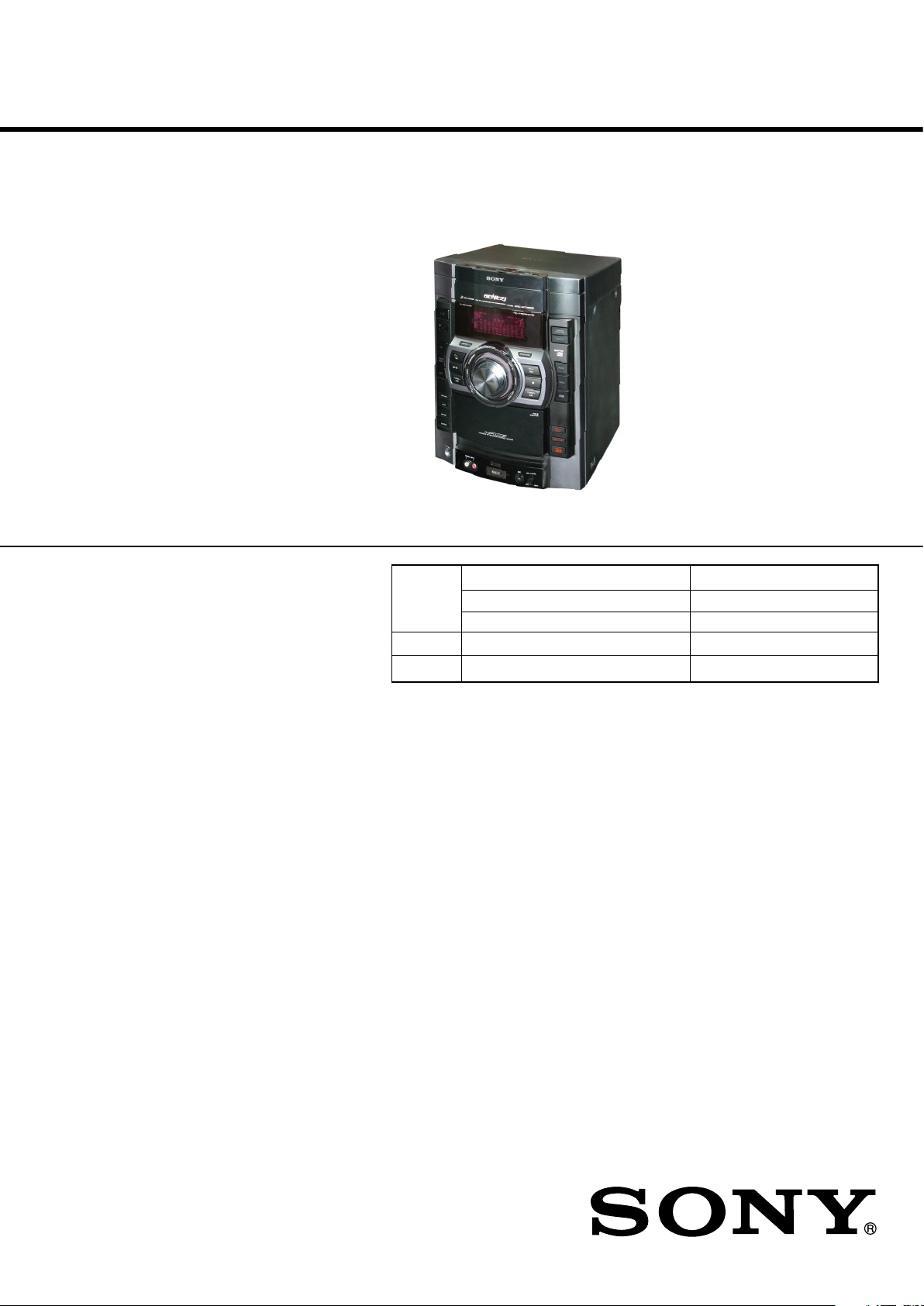
Photo : HCD-GTX888 (E Model)
Model Name Using Similar Mechanism HCD-GTX66/GTX77/GTX88
CD CD Mechanism Type CDM74KF-K6BD93-WOD//M
Section
Tape Deck Model Name Using Similar Mechanism NEW
Section Tape Mechanism Type CFP42608
Optical Pick-up Name KSM-213DCP/C2NP
AEP Model
HCD-GTX777
E Model
HCD-GTX777/GTX787/GTX888
Australian Model
HCD-GTX888
AUDIO POWER SPECIFICATION
Amplifi er section
MHC-GTX888 (HCD-GTX888)
The following are measured at
Mexican model: AC 127 V, 60 Hz
Other models: AC 120, 220, 230 – 240 V, 50/60 Hz
Front/Surround speaker
Power Output (rated): 190 W + 190 W (at 8 Ω and 24 Ω,
1 kHz, 1% THD, at LINK MODE)
RMS output power (reference):
295 W + 295 W (per channel at 8 Ω and
24 Ω, 1 kHz, 10% THD, at LINK MODE)
Subwoofer
RMS output power (reference):
160 W + 160 W (per channel at 6 Ω,
100 Hz, 10% THD)
SPECIFICATIONS
MHC-GTX787 (HCD-GTX787)
The following are measured at
Mexican model: AC 127 V, 60 Hz
Other models: AC 120, 220, 230 – 240 V, 50/60 Hz
Front speaker
Power Output (rated): 230 W + 230 W (at 4 Ω, 1 kHz, 1% THD)
RMS output power (reference):
380 W + 380 W (per channel at 4 Ω, 1 kHz, 10% THD)
MHC-GTX777 (HCD-GTX777)
European model only
The following are measured at
AC 230 V, 50/60 Hz
Front/Surround speaker
Power Output (rated): 235 W + 235 W (at 8 Ω and 8 Ω, 1 kHz,
1% THD, at LINK MODE)
RMS output power (reference):
380 W + 380 W (per channel at 8 Ω and
8 Ω, 1 kHz, 10% THD, at LINK MODE)
– Continued on next page –
CD DECK RECEIVER
9-890-504-02
2008E08-1
© 2008. 05
Sony Corporation
Audio Business Group
Published by Sony EMCS (Malaysia) PG Tec
1
Page 2

HCD-GTX777/GTX787/GTX888
Other models
The following are measured at
AC 120, 220, 230 – 240 V, 50/60 Hz
Front/Surround speaker
Power Output (rated): 235 W + 235 W (at 8 Ω and 8 Ω, 1 kHz,
1% THD, at LINK MODE)
RMS output power (reference):
380 W + 380 W (per channel at 8 Ω and
8 Ω, 1 kHz, 10% THD, at LINK MODE)
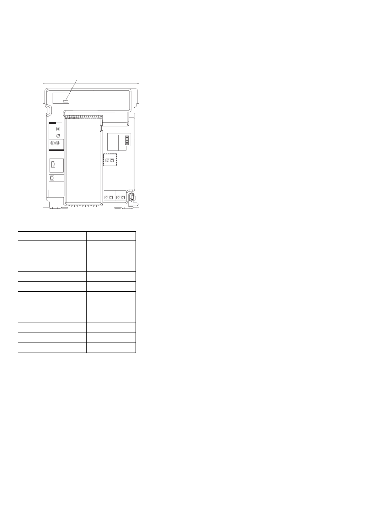
Inputs
VIDEO (AUDIO IN) L/R:
Voltage 250 mV, impedance 47 kilohms
AUDIO INPUT L/R: Voltage 450 mV, impedance 47 kilohms
MIC: Sensitivity 1 mV, impedance 10 kilohms
(USB) port: Type A
Outputs
PHONES: accepts headphones of 8 Ω or more
Disc player section
System Compact disc and digital audio system
Laser Semiconductor laser
(λ = 770 – 810 nm)
Emission duration: continuous
Laser Output Max. 44.6 µW*
* This output is the value measured at
a distance of 200 mm from the
objective lens surface on the Optical
Pick-up Block with 7 mm aperture.
Frequency response 20 Hz – 20 kHz
Wave length 770 – 810 nm
Signal-to-noise ratio More than 90 dB
Dynamic range More than 88 dB
Tape deck section
Recording system 4-track 2-channel stereo
Frequency response 50 – 13,000 Hz (±3 dB),
using Sony TYPE I tape
Wow and fl utter ±0.35% W.Peak (IEC)
0.3% W.RMS (NAB)
±0.4% W.Peak (DIN)
Tuner section
FM stereo, FM/AM superheterodyne tuner
FM tuner section
Tuning range
Brazil model: 87.5 – 108.0 MHz (100 kHz step)
Other models: 87.5 – 108.0 MHz (50 kHz step)
Antenna FM lead antenna
Antenna terminals 75 ohms unbalanced
Intermediate frequency 10.7 MHz
AM tuner section
Tuning range Pan-American and Oceanian models:
530 – 1,710 kHz (with the interval set at 10 kHz)
531 – 1,710 kHz (with the interval set at 9 kHz)
European model: 531 – 1,602 kHz (with the interval set at 9 kHz)
Other models: 531 – 1,602 kHz (with the interval set at 9 kHz)
530 – 1,610 kHz (with the interval set at 10 kHz)
Antenna AM loop antenna
Antenna terminals External antenna terminal
Intermediate frequency 450 kHz
USB section
Supported bit rate MP3 (MPEG 1 Audio Layer 3): 32 – 320 kbps, VBR
WMA: 32 – 192 kbps, VBR AAC: 48 – 320 kbps
Sampling frequencies MP3 (MPEG 1 Audio Layer 3): 32/44.1/48 kHz
WMA: 44.1 kHz, AAC: 44.1 kHz
Transfer speed Full-Speed
Supported USB device Mass Storage Class
Maximum current 500 mA
General
Power requirements
European model: 230 V AC, 50/60 Hz
Mexican model: 127 V AC, 60 Hz
Oceanian model: 230 – 240 V AC, 50/60 Hz
Argentina models: 220 V AC, 50/60 Hz
Other models: 120 V, 220 V or 230 – 240 V AC, 50/60 Hz,
adjustable with voltage selector
Power consumption MHC-GTX888: 430 W
MHC-GTX787/MHC-GTX777: 300 W
Dimensions (w/h/d) (Approx.)
HCD-GTX888/HCD-GTX787/
HCD-GTX777: 281 × 365 × 454 mm
(11 1/8 × 14 3/8 × 17 7/8 inches)
Mass (Approx.) HCD-GTX888: 14.0 kg (30 lb 14 oz)
HCD-GTX787/HCD-GTX777:
12.0 kg (26 lb 8 oz)
Supplied accessories Remote Commander (1)
R6 (size AA) batteries (2)
AM loop antenna (1)
FM lead antenna (1)
Front speaker pads (8)
Surround speaker pads
(MHC-GTX888/MHC-GTX777 only) (8)
Subwoofer pads (MHC-GTX888 only) (Black) (8)
Speaker cords (MHC-GTX787 only) (2)
Spacer A (MHC-GTX888 only) (2)
Spacer B (MHC-GTX888 only) (2)
Spacer C (MHC-GTX777 only) (2)
Audio cable (1) (Mexico only)
Design and specifi cations are subject to change without notice.
SAFETY-RELATED COMPONENT WARNING!!
COMPONENTS IDENTIFIED BY MARK 0 OR DOTTED LINE
WITH MARK 0 ON THE SCHEMATIC DIAGRAMS AND IN THE
PARTS LIST ARE CRITICAL TO SAFE OPERATION. REPLACE
THESE COMPONENTS WITH SONY PARTS WHOSE PART
NUMBERS APPEAR AS SHOWN IN THIS MANUAL OR IN
SUPPLEMENTS PUBLISHED BY SONY.
2
Page 3
HCD-GTX777/GTX787/GTX888
Notes on Chip Component Replacement
• Never reuse a disconnected chip component.
• Notice that the minus side of a tantalum capacitor may be
damaged by heat.
Flexible Circuit Board Repairing
• Keep the temperature of soldering iron around 270°C during
repairing.
• Do not touch the soldering iron on the same conductor of the
circuit board (within 3 times).
• Be careful not to apply force on the conductor when soldering or
unsoldering.
UNLEADED SOLDER
Boards requiring use of unleaded solder are printed with the lead
free mark (LF) indicating the solder contains no lead.
(Caution: Some printed circuit boards may not come printed with
the lead free mark due to their particular size)
: LEAD FREE MARK
Unleaded solder has the following characteristics.
• Unleaded solder melts at a temperature about 40 °C higher than
ordinary solder.
Ordinary soldering irons can be used but the iron tip has to be
applied to the solder joint for a slightly longer time.
Soldering irons using a temperature regulator should be set to
about 350 °C.
Caution: The printed pattern (copper foil) may peel away if the
heated tip is applied for too long, so be careful!
• Strong viscosity
Unleaded solder is more viscou-s (sticky, less prone to fl ow) than
ordinary solder so use caution not to let solder bridges occur such
as on IC pins, etc.
• Usable with ordinary solder
It is best to use only unleaded solder but unleaded solder may also
be added to ordinary solder.
NOTES ON LASER DIODE EMISSION CHECK
The laser beam on this model is concentrated so as to be focused on
the disc refl ective surface by the objective lens in the optical pick-up
block. Therefore, when checking the laser diode emission,
observe from more than 30 cm away from the objective lens.
Laser component in this product is capable
of emitting radiation exceeding the limit for
Class 1.
This appliance is
claassifi ed as a CLASS 1
LASER product. This
label is located on the
rear exterior.
CAUTION
Use of controls or adjustments or performance of procedures
other than those specifi ed herein may result in hazardous
radiation exposure.
NOTES ON HANDLING THE OPTICAL PICK-UP BLOCK
OR BASE UNIT
The laser diode in the optical pick-up block may suffer electrostatic
breakdown because of the potential difference generated by the
charged electrostatic load, etc. on clothing and the human body.
During repair, pay attention to electrostatic break-down and also
use the procedure in the printed matter which is included in the
repair parts.
The fl exible board is easily damaged and should be handled with
care.
3
Page 4
HCD-GTX777/GTX787/GTX888
MODEL IDENTIFICATION
– MODEL NUMBER LABEL –
PART NO
(GTX888 ONLY)
• Abbreviation
E2 : 120V AC area in E model
E3 : Middle Easten, African and Indian model
E51 : Chilean and Peruvian model
AR : Argentina model
AUS : Australian model
MX : Mexican model
(GTX888 ONLY)
MODEL Parts No
GTX888: E2, E51
GTX777: E2, E51
GTX787: E2
GTX777: AEP
GTX888: AR
GTX777: AR
GTX888: AUS
GTX888: E3
GTX777: E3
GTX888: MX
GTX777: MX
3-290-078-0s
3-290-078-1s
3-290-078-2s
3-290-079-1s
3-873-456-0s
3-873-456-1s
3-873-457-0s
3-873-458-0s
3-873-458-1s
3-873-459-0s
3-873-459-1s
4
Page 5

TABLE OF CONTENTS
HCD-GTX777/GTX787/GTX888
1. GENERAL
Guide to parts and controls ...................................................... 6
2. DISASSEMBLY
2-1. Case (Top) .......................................................................... 13
2-2. Loading Panel .................................................................... 13
2-3. CD Block Section .............................................................. 14
2-4. Front Panel Section ............................................................ 14
2-5. Tape Mechanism Deck, Mic Board,
USB Connector Board ....................................................... 15
2-6. Panel Board, Function Board, Jog Board .......................... 15
2-7. CD-SW Board .................................................................... 16
2-8. Cover (CDM) ..................................................................... 16
2-9. Tuner Pack ......................................................................... 17
2-10. Back Panel Section, Sub Trans Board ............................... 17
2-11. Main Board ....................................................................... 18
2-12. Power Board Section ......................................................... 18
2-13. Subwoofer Board, Power Board ........................................ 19
2-14. Power Transformer (T1200) .............................................. 19
2-15. BD93 Board ....................................................................... 20
2-16. Driver Board, SW Board, USB Board ............................... 20
2-17. Optical Pick-up .................................................................. 21
2-18. Sensor Board ...................................................................... 21
2-19. Motor (TB) Board .............................................................. 22
2-20. Motor (LD) Board ............................................................. 22
3. TEST MODE .............................................................. 23
4. MECHANICAL ADJUSTMENTS ......................... 27
5. ELECTRICAL ADJUSTMENTS ..........................28
6. DIAGRAMS
6-1. Block Diagram — RF/Servo Section — ........................... 31
6-2. Block Diagram — Tape/Tuner Section — ......................... 32
6-3. Block Diagram — Main Section — .................................. 33
6-4. Block Diagram — USB Section — ................................... 34
6-5. Block Diagram — AMP/Subwoofer Section — ................ 35
6-6. Block Diagram — Display/Power Section — ................... 36
6-7. Circuit Boards Location ..................................................... 37
6-8. Printed Wiring Board — BD93 Board — ......................... 40
6-9. Schematic Diagram — BD93 Board — ............................ 41
6-10. Printed Wiring Boards — Driver Board — ....................... 42
6-11. Schematic Diagram — Driver Board — ........................... 43
6-12. Printed Wiring Board — Main Board — ........................... 44
6-13. Schematic Diagram — Main Board (1/4) — ..................... 45
6-14. Schematic Diagram — Main Board (2/4) — ..................... 46
6-15. Schematic Diagram — Main Board (3/4) — ..................... 47
6-16. Schematic Diagram — Main Board (4/4) — ..................... 48
6-17. Printed Wiring Board — USB Board — ........................... 49
6-18. Schematic Diagram — USB Board — .............................. 50
6-19. Printed Wiring Board — Panel Function Board — ........... 51
6-20. Schematic Diagram — Panel Function Board — .............. 52
6-21. Printed Wiring Board — Power Board — ......................... 53
6-22. Schematic Diagram — Power Board — ............................ 54
6-23. Printed Wiring Board — Sub Woofer Board — ................ 55
6-24. Schematic Diagram — Sub Woofer Board — ................... 56
6-25. Printed Wiring Boards — Trans Board — ......................... 57
6-26. Schematic Diagram — Trans Board — ............................. 58
6-27. Printed Wiring Board — Illumination Board — ............... 59
6-28. Schematic Diagram — Illumination Board — .................. 60
6-29. Printed Wiring Board — MIC Board — ........................... 61
6-30. Schematic Diagram — MIC Board — .............................. 62
6-31. Printed Wiring Boards — TC Board — ............................ 63
6-32. Schematic Diagram — TC Board — ................................. 64
6-33. Printed Wiring Boards — Meter Display Board — .......... 65
6-34. Schematic Diagram — Meter Display Board — ............... 66
7. EXPLODED VIEWS
7-1. Main Section ...................................................................... 80
7-2. Back Panel Section ............................................................ 81
7-3. Front Panel Section (1) ...................................................... 82
7-4. Front Panel Section (2) ...................................................... 83
7-5. Meter Display Assy ........................................................... 84
7-6. Chassis Section .................................................................. 85
7-7. CD Mechanism Section (1) ............................................... 86
7-8. CD Mechanism Section (2) ............................................... 87
8. ELECTRICAL PARTS LIST ................................. 88
5
Page 6
HCD-GTX777/GTX787/GTX888
XLX
X
X
SECTION 1
GENERAL
Note:
This section is extracted
from instruction manual.
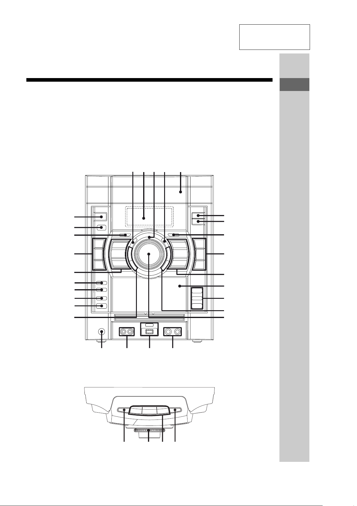
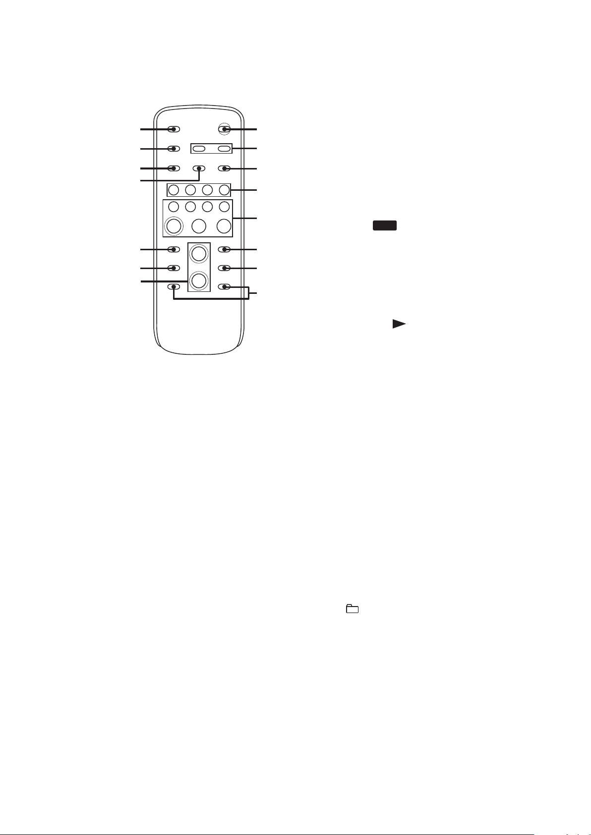
Guide to parts and controls
This manual mainly explains operations using the buttons on the unit, but the same
operations can also be performed using the buttons on the remote having the same or
similar names.
Unit
– Front view
Guide to parts and controls
– Top view
XH
XG
XE
R
XT
XB
X
RM
RE
RKRL RI
R
RB
RT
RE
RG
RH
M
6
K
I
Continued
M
Page 7
HCD-GTX777/GTX787/GTX888
Remote
FI
XE
FH
FG
FE
FT
RG
" EQ BAND/MEMORY (page 38)
Press to select a frequency band.
# Display (pages 11, 31, 32, 48)
Meter display (page 32)
$ Power illuminator (pages 31, 32)
XH
F
FB
R
RM
XM
R
) METER MODE (page 32)
Press to select a preset display
pattern.
* Function buttons:
CD (pages 15, 20, 24, 32, 33, 36)
TUNER/BAND (pages 22, 32)
Unit: TAPE (pages 29, 32)
Unit: AUDIO (pages 29, 32)
Unit: VIDEO (pages 29, 32)
Unit: (pages 25, 27, 32, 33)
USB
Remote: USB (pages 25, 27, 33)
Remote: FUNCTION (page 29)
Press to select a function.
+ Unit: /9 (play/pause)
(pages 20, 24, 27, 29, 44)
Remote: (play) (pages 20,
27, 29, 44)
Remote: 9 (pause) (pages 20,
29)
Press to start or pause playback.
Y (stop) (pages 20, 22, 27, 29,
37, 43)
Press to stop playback, recording or
transferring.
% PRESET EQ (pages 30, 38)
Press to select a preset sound effect.
& Disc tray (pages 11, 20, 43, 48)
' SURROUND SPEAKER MODE
(MHC-GTX888 only) (page 30)
Press to select the sound system.
SURROUND
(MHC-GTX787/MHC-GTX777
only) (page 30)
Press to select the surround effect.
( GROOVE (page 30)
Press to reinforce the bass.
(go backward/go
forward) (pages 20, 27, 34)
Press to select a track or file.
Unit: TUNING +/– (page 22)
Remote: +/– (tuning) (pages 22,
35)
Press to tune in a radio station.
+/– (pages 20, 27, 33, 36)
Press to select a folder.
N.(rewind/fast forward)
(pages 20, 28, 29)
Unit: Press to fast forward or rewind.
Remote: Press to find a point in a
track or file.
7
Page 8
HCD-GTX777/GTX787/GTX888
, PUSH ;OPEN/CLOSE
(page 29)
Press to insert or eject a tape.
Tape deck (pages 29, 36, 40, 47)
- REC TO TAPE (page 37)
Press to record onto a tape.
REC TIMER (page 40)
Press to set the Recording Timer.
REC TO (page 24)
Press to transfer onto the connected
optional USB device.
. FLANGER (pages 31, 43, 47)
DELAY (pages 31, 43, 47)
CHORUS (pages 31, 43, 47)
SOUND FLASH (page 31)
Press to create a party atmosphere.
/ Unit: MASTER VOLUME
(pages 20, 27, 29, 31, 42)
Turn to adjust the volume.
Remote: VOLUME +/–*
(pages 20, 27, 29, 31, 42)
Press to adjust the volume.
USB
0 MIC (jack) (pages 39, 42, 53)
Connect an optional microphone.
MIC LEVEL (pages 37, 39, 42)
Turn to adjust the microphone
volume.
1 (indicator)
Lights up when transferring to the
connected optional USB device, or
when erasing audio files or folders.
(USB) port (pages 23, 25,
27, 46, 53)
Connect an optional USB device.
2 AUDIO INPUT L/R (jacks)
(page 29)
Connect to an audio component
(Portable audio player, etc.).
3 PHONES (jack) (pages 42, 53)
Connect the headphones.
4 ENTER (pages 20, 27, 30, 31,
34, 35, 38)
Press to enter the selection.
5 RETURN (page 20)
Press to return to the parent folder.
Press to exit search mode.
Guide to parts and controls
* The VOLUME + button has a tactile dot.
Use the tactile dot as a reference when
operating the system.
6 ERASE (page 25)
Press to erase audio files or folders
on the connected optional USB
device.
Continued
M
8
Page 9

HCD-GTX777/GTX787/GTX888
7 OPTIONS (pages 30, 31)
Press to select the display pattern,
MP3 BOOSTER+ function and USB
SELECT.
8 DISPLAY (pages 19, 32, 32, 36)
Press to change the information in
the display.
9 IR Receptor (page 42)
: (on/standby) (pages 14, 15,
42, 48)
Press to turn the system on or off.
; OPEN/CLOSE ; (pages 15, 20,
43)
Press to load or eject a disc.
XK DISC 1 ~ 3 (pages 21, 33)
Press to select a disc.
Press to switch to CD function from
other function.
XL OPERATION DIAL (pages 20,
27, 31, 38)
Turn to select a track, file or folder.
Turn to select a setting.
XM Unit: DISC SKIP/EX-CHANGE
(pages 15, 20, 21, 33)
Press to select a disc.
Press to exchange other discs during
playback.
F CLOCK/TIMER SELECT
(page 40)
CLOCK/TIMER SET (pages 19,
40)
Press to set the clock and the timers.
F[ REPEAT/FM MODE (pages 20,
23, 28, 47)
Press to change the Repeat Play
setting.
Press to select the FM monaural or
stereo reception.
FT EQ (pages 30, 38)
Press to select a preset sound effect.
FE CLEAR (page 34)
Press to delete a pre-programmed
track.
FG PLAY MODE/TUNING MODE
(pages 21, 22, 28, 33, 35, 37, 44,
48)
Press to select the play mode of CD
or USB function.
Press to select the tuning mode.
FH TUNER MEMORY (page 35)
Press to preset a radio station.
FI SLEEP (page 39)
Press to activate the Sleep Timer.
Remote: DISC SKIP (pages 21,
33)
Press to select a disc.
9
Page 10
HCD-GTX777/GTX787/GTX888
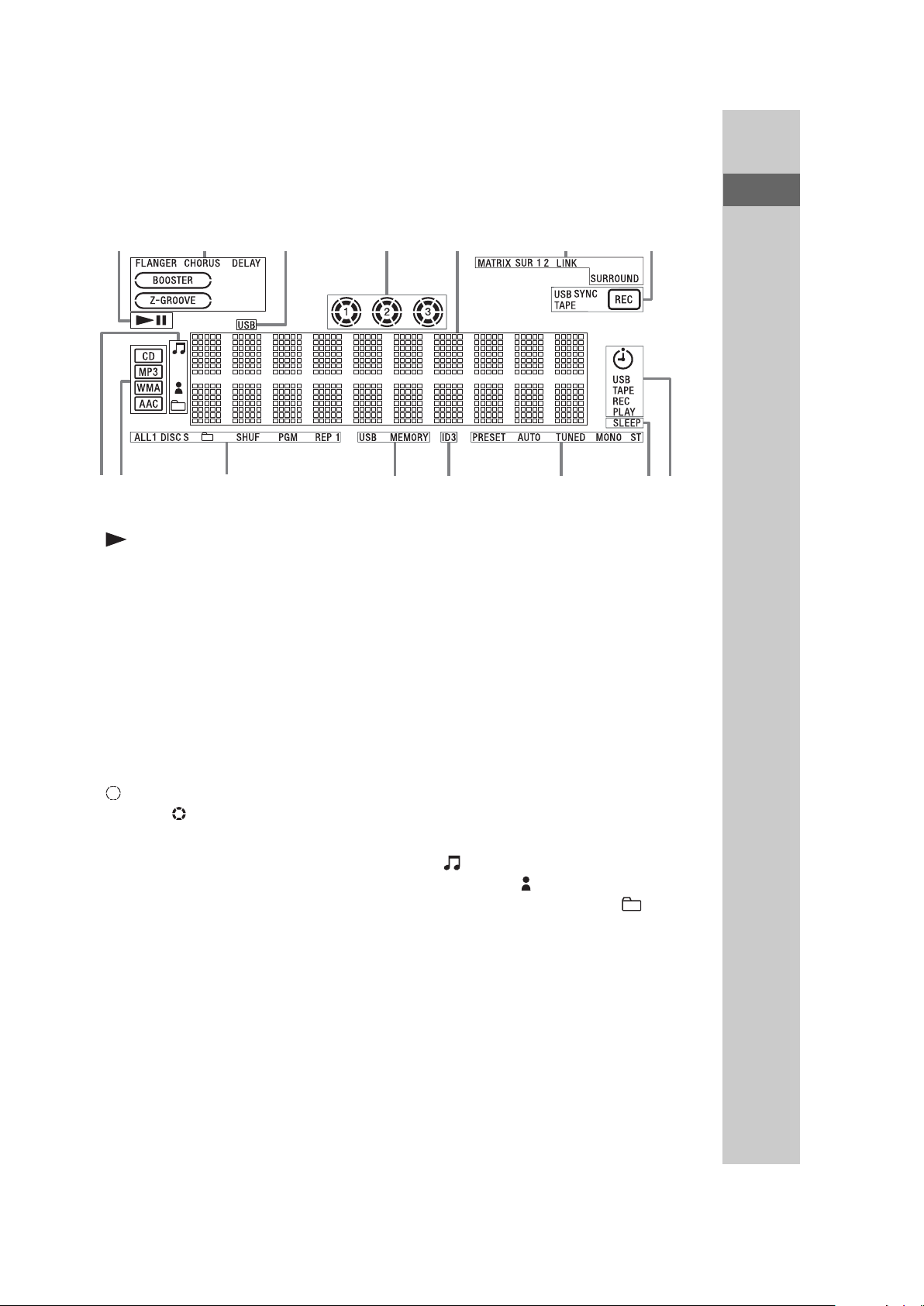
– Display
Guide to parts and controls
RERG
" “ ” lights up during playback.
“/9” lights up when playback is
paused.
# Indicates the activated sound effect
(pages 30, 31, 38).
Note
“LINK”, “MATRIX SUR 1” and
“MATRIX SUR 2” light up for
MHC-GTX888 only.
$ Lights up when the USB function is
selected (page 27).
% Indicators for the disc tray (page 20).
“ ” lights up when the disc is
selected. “ ” lights up when there is
a disc on the disc tray. “1”, “2” and
“3” light up when the system is turned
on.
& Displays the current status and
information (page 32).
' Lights up during transferring onto an
USB device or recording onto a tape
(pages 23, 36).
RBRT
R
( Lights up when the timer is set
(page 39).
) Lights up when the Sleep Timer is
activated (page 39).
* Indicators for the TUNER function
(pages 22, 35).
+ Lights up when the MP3 file contains
ID3 tag information.
, Lights up when an optional USB
device is recognized (page 23).
- Indicates the selected play mode
(pages 21, 28).
. Indicates the type of disc or file that
the system recognized.
/ Indicates the type of audio file
information that displayed (page 32).
“ ” lights up when a file name is
displayed. “ ” lights up when an
artist name is displayed. “ ” lights
up when a folder name is displayed.
10
Page 11
Using the subwoofers
(MHC-GTX888 only)
You can use the subwoofers to enhance
the bass.
Subwoofer A (SS-WG888A)
1 Press SUBWOOFER ON/OFF on
the subwoofer A to light up the
indicator.
HCD-GTX777/GTX787/GTX888
The subwoofers are turned on.
2 Turn SUBWOOFER LEVEL on the
subwoofer A to adjust the level.
11
Page 12
HCD-GTX777/GTX787/GTX888
SECTION 2
DISASSEMBLY
Note : This set can be disassembled in the order shown below.
SET
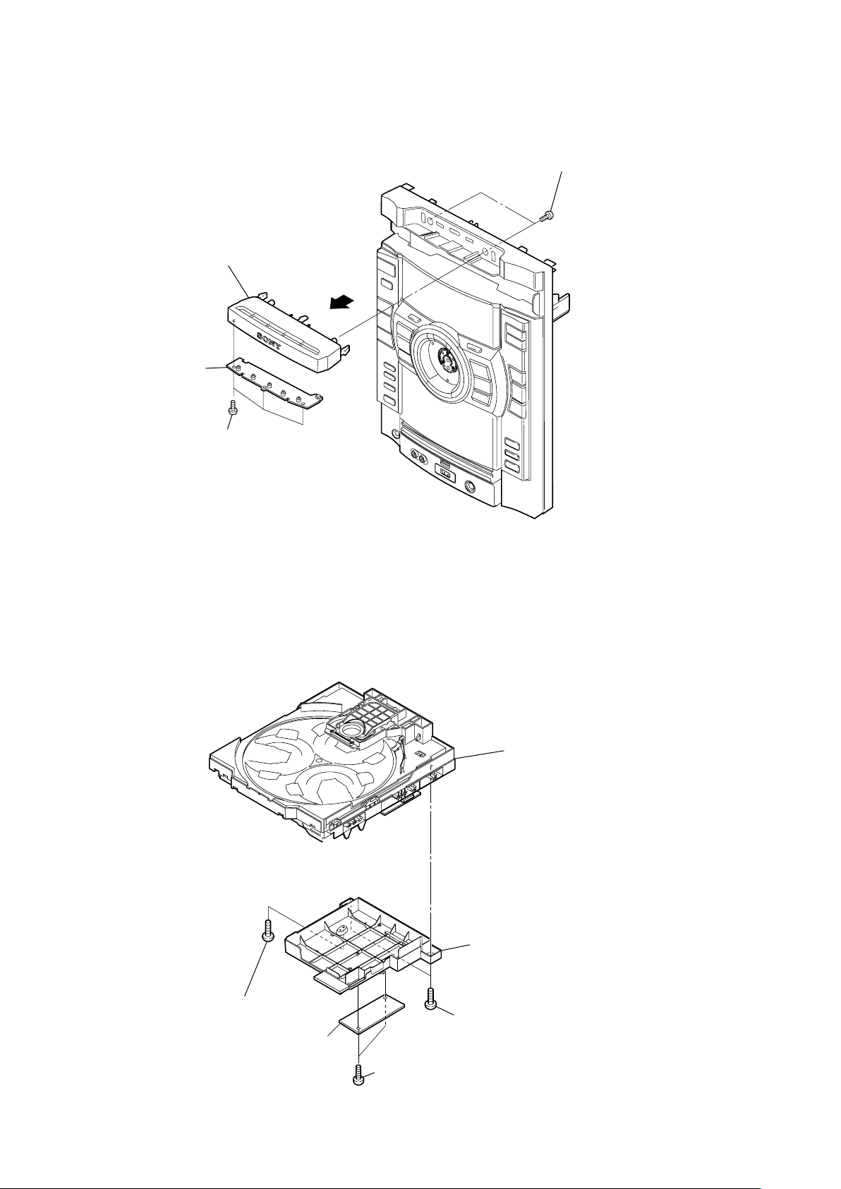
2-1. CASE (TOP)
(Page 13)
2-2. LOADING PANEL
(Page 13)
2-8. COVER (CDM)
(Page 16)
2-3. CD BLOCK SECTION
(Page 14)
2-4. FRONT PANEL SECTION
(Page 14)
2-5. TAPE MECHANISM DECK,
MIC BOARD,
USB CONNECTOR BOARD
(Page 15)
2-9. TUNER PACK
(Page 17)
2-10. BACK PANEL SECTION,
SUB TRANS BOARD
(Page 17)
2-16. DRIVER BOARD,
SW BOARD,
USB BOARD
(Page 20)
2-18. SENSOR BOARD
(Page 21)
2-19. MOTOR (TB) BOARD
(Page 22)
2-20. MOTOR (LD) BOARD
(Page 22)
2-6. METER DISPLAY ASSY
PANEL BOARD,
FUNCTION BOARD,
JOG BOARD
(Page 15)
2-7. CD-SW BOARD
(Page 16)
2-15. BD93 BOARD
(Page 20)
2-17. OPTICAL PICK-UP
(Page 21)
2-11. MAIN BOARD
(Page 18)
2-12. POWER BOARD SECTION
(Page 18)
2-13. SUBWOOFER BOARD,
POWER BOARD
(Page 19)
12
2-14. POWER TRANSFORMER
(T1200)
(Page 19)
Page 13
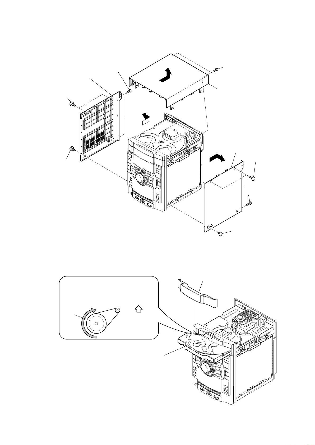
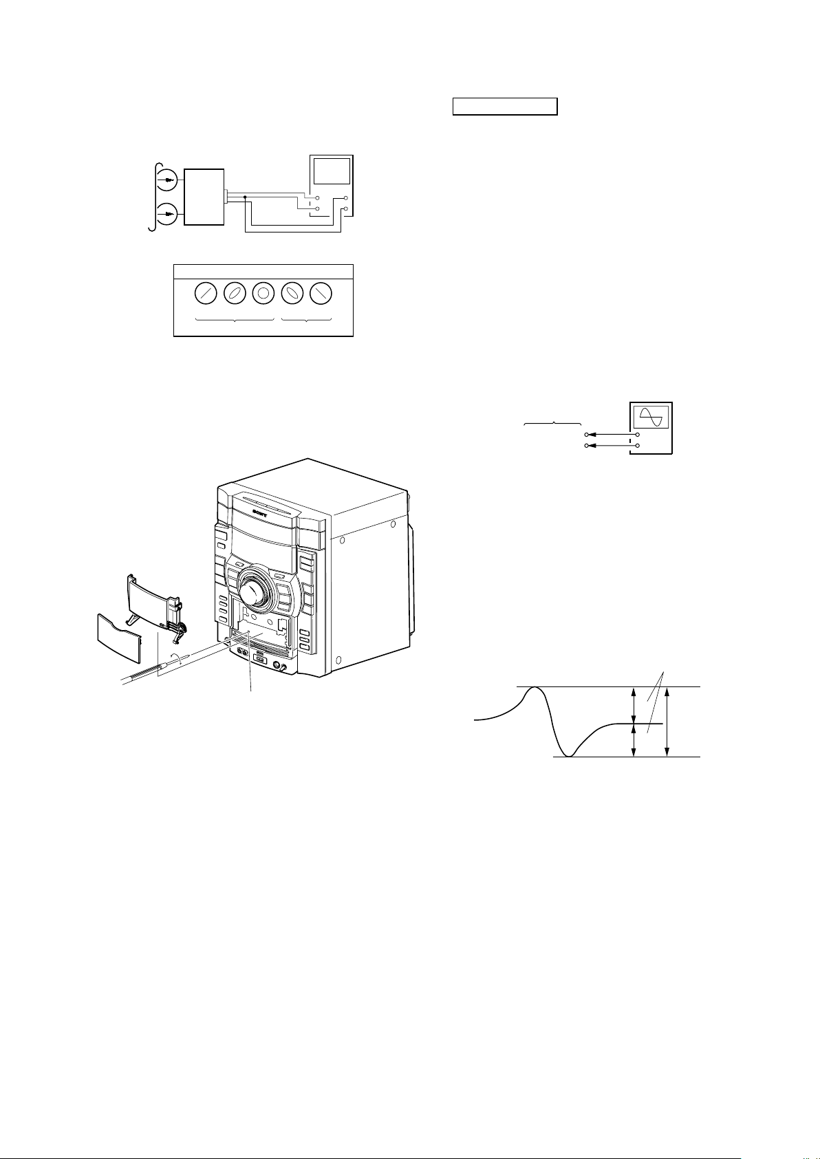
Note : Follow the disassembly procedure in the numerical order given.
2-1. CASE (TOP)
two screws
(+BVTP 3 x 10)
panel (side-L)
two
screws
(case 3 TP2)
screw
(case 3 TP2)
RT
HCD-GTX777/GTX787/GTX888
RB
two screws
(+BVTP 3 x 10)
RE
case (top)
panel (side-R)
two
screws
(case 3 TP2)
2-2. LOADING PANEL
CD mechanism deck (CDM74KF)
Turn the pulley to the direction of the arrow.
pulley
Front panel side
loading panel
two screws
(+BVTP 3 x 10)
screw
(case 3 TP2)
Pull-out the disc tray.
13
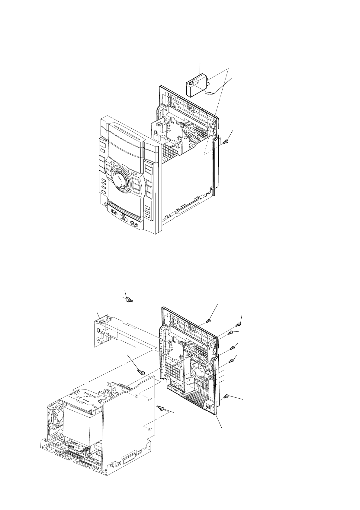
Page 14
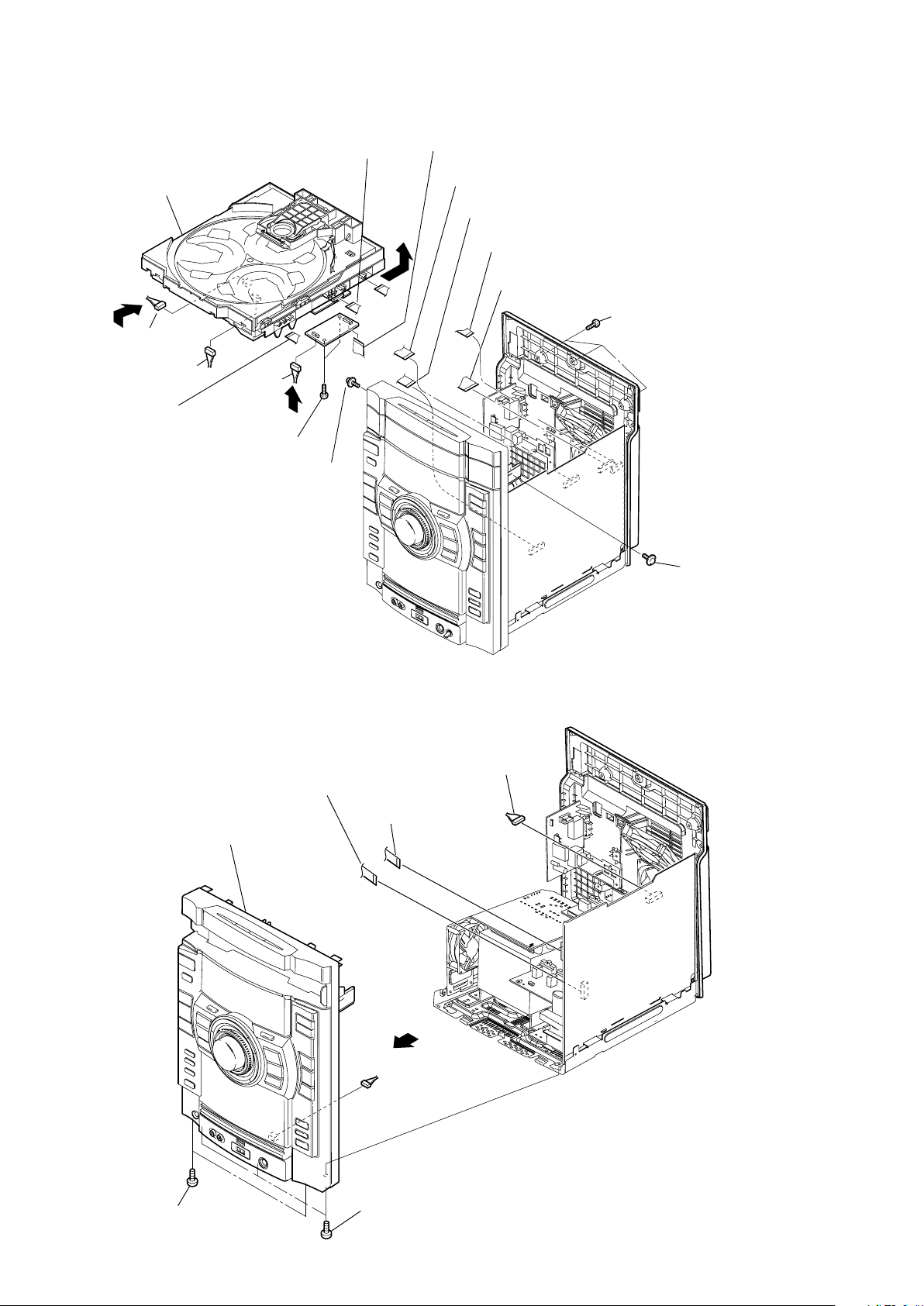
HCD-GTX777/GTX787/GTX888
Ver. 1.1
2-3. CD BLOCK SECTION
wire (flat type) (13 core)
(CN701)
RB
CD block section
CN901 (2P)
CN903 (5P)
RT
Wire (flat type) (21 core)
(CN907)
RE
CN400
(8p)
RG
two screws
(+BVTP 3
a
x 10)
tapping screw
wire (flat type) (11 core)
(CN410 )
wire (flat type) (13 core)
(CN110)
RH
wire (flat type) (11 core)
(CN102)
wire (flat type) (31 core)
(CN430)
wire (flat type) (21 core)
a
c
(CN204)
screws
three
(+BVTP 3
c
a
b
x 12)
c
b
b
d
d
2-4. FRONT PANEL SECTION
front panel section
wire (flat type) (7 core)
(CN115)
wire (flat type) (25 core)
(CN114)
CN101 (7P)
d
tapping screw
14
two screws
(+BVTP 3 x 10)
screws
three
(+BVTP 3 x 10)
Page 15
HCD-GTX777/GTX787/GTX888
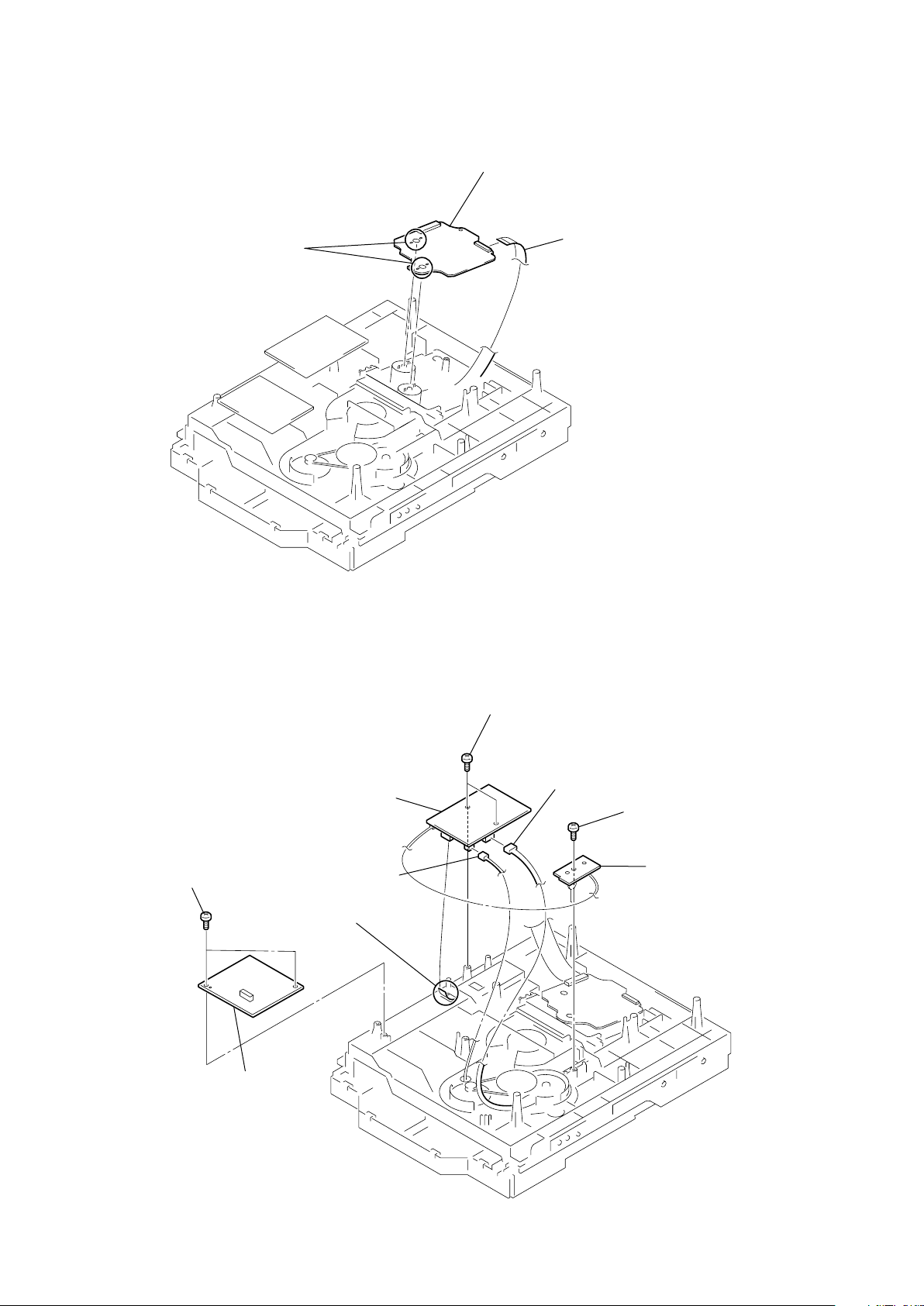
2-5. TAPE MECHANISM DECK, MIC BOARD, USB CONNECTOR BOARD
tape mechanism deck
four screws
(+BVTP 2.6 (3CR))
three screws
(+BVTP 2.6 (3CR))
knob (MIC)
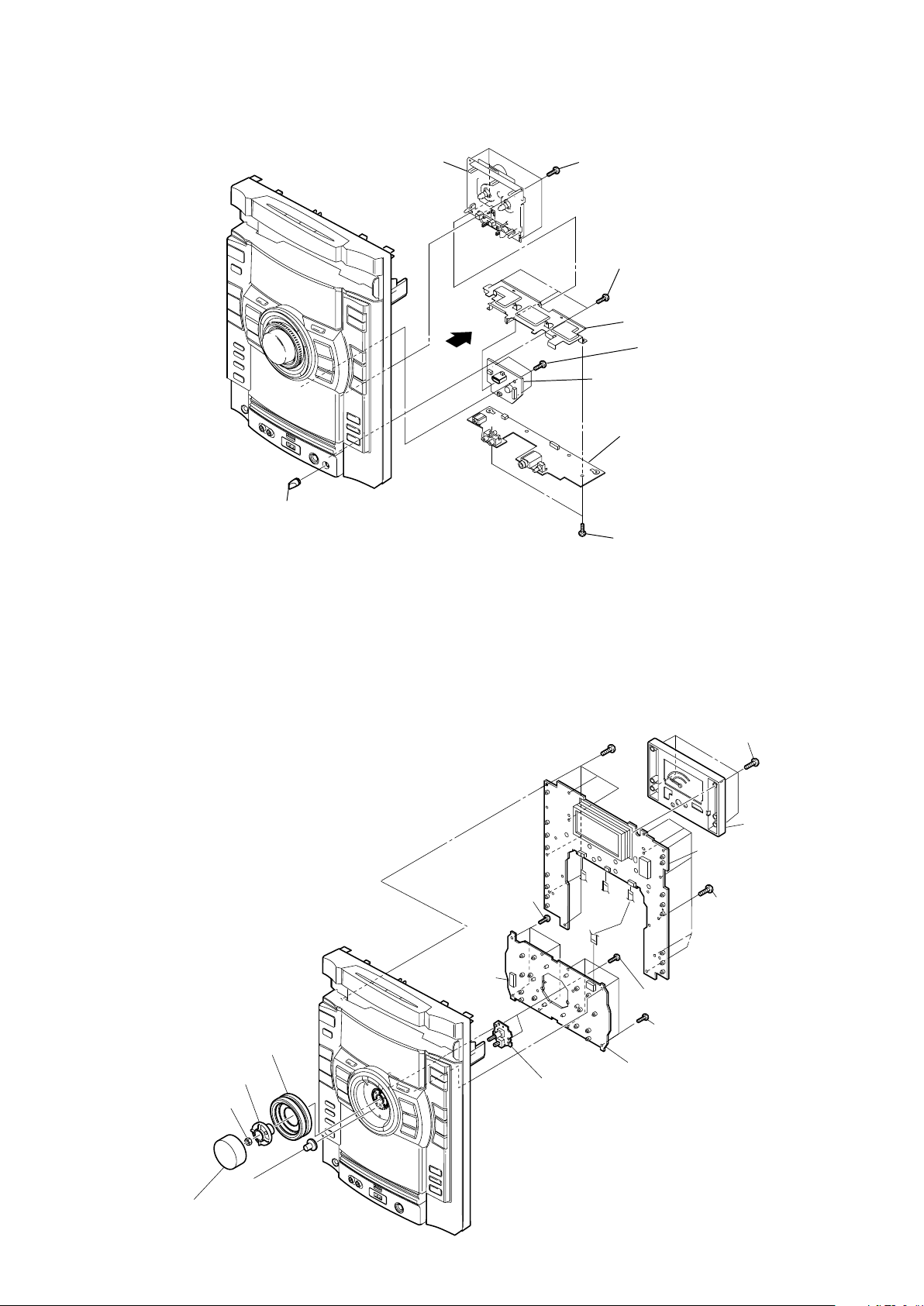
2-6. PANEL BOARD, FUNCTION BOARD, JOG BOARD
bracket (MIC shield)
(+BVTP 2.6 (3CR))
USB CONNECTOR board
MIC board
two
(+BVTP 2.6 (3CR))
six screws
(+BVTP 2.6 (3CR))
three screws
screws
four
(+BVTP 2.6 (3CR))
screws
RE
knob jog assy
RT
holder (jog)
RB
nut
knob (volume)
RG
gear (encoder)
four screws
(+BVTP 2.6 (3CR))
b
RH
JOG board
meter display assy
panel board
b
a
two screws
(+BVTP 2.6 (3CR))
four screws
(+BVTP 2.6 (3CR))
illumination board
six screws
(+BVTP 2.6 (3CR))
15
Page 16
HCD-GTX777/GTX787/GTX888
Ver. 1.1
2-7. CD-SW BOARD
escucheon (CD)
CD-SW board
three
(+BVTP 2.6 (3CR))
screws
screws
two
(+BVTP 2.6 (3CR))
2-8. COVER (CDM), TC BOARD
one screw
(+BVTP 3
TC board
CD mechanism deck
cover (CDM)
s
10)
two screws
(+BVTP 3
s
10)
16
two screw
(+BVTP 2.6 (3CR))
Page 17
2-9. TUNER PACK
tuner pack
HCD-GTX777/GTX787/GTX888
Ver. 1.1
wire (flat type) (9 core)
(CN1)
two
screws
(+BVTP 3 x 8)
2-10. BACK PANEL SECTION, SUB TRANS BOARD
CN1203 (4P)
sub trans board
CN206 (3P)
CN202 (3P)
two screws
(+BVTP 3
(+BVTP 3 s10)
(+BVTP 3 s10)
two screws
three screws
(+BVTP 3 s10)
RB
back panel section
s
10)
one
screw (GTX888 only)
one
screw (GTX888 only)
one screw
two screws
three screws
(+BVTP 3 s10)
(+BVTP 3 s10)
(+BVTP 3 s10)
(+BVTP 3 s10)
(GTX787)
(GTX777/GTX888)
(GTX777/GTX787)
(GTX888)
17
Page 18
HCD-GTX777/GTX787/GTX888
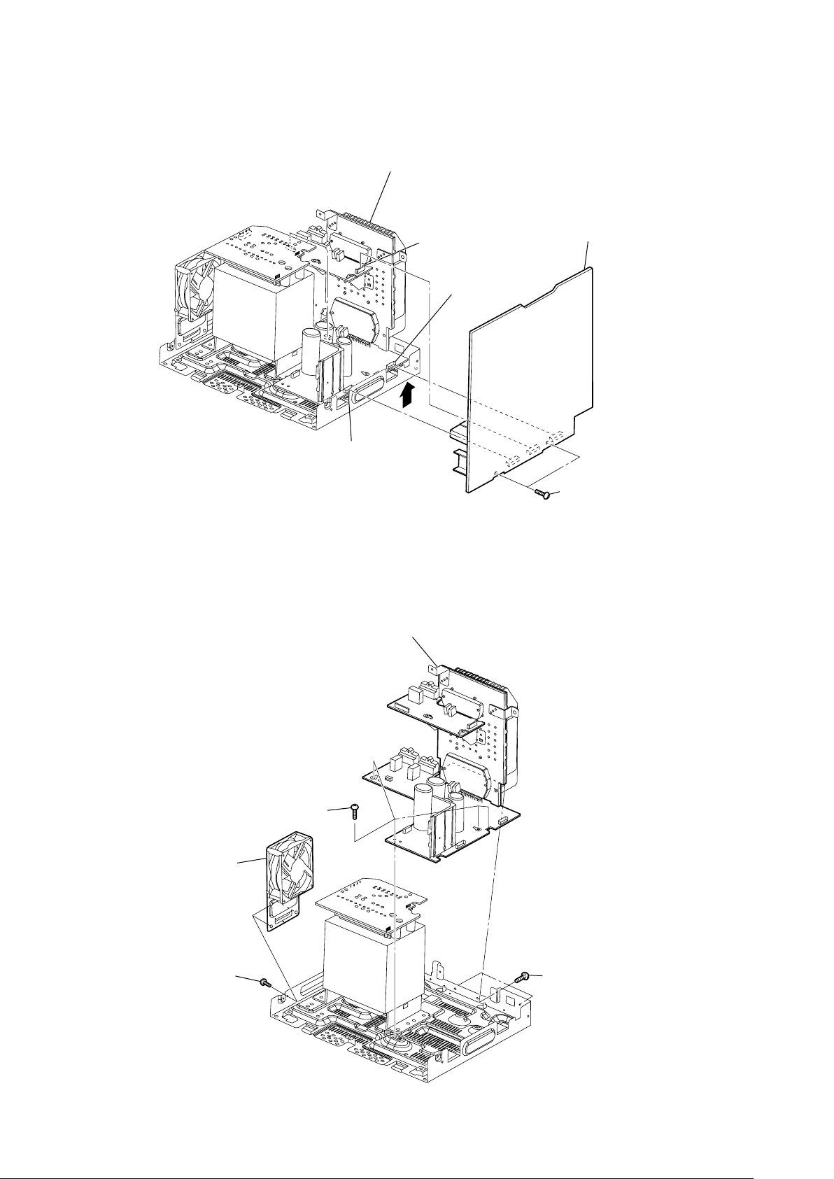
2-11. MAIN BOARD
POWER board assy
CN809 (9 pin)
CN610
(8 pin)
MAIN board
CN611
(8 pin)
2-12. POWER BOARD SECTION, DC FAN (FOR GTX888)
POWER board section
four screws
(+BV3 (3-CR))
two screws
(+BV3 (3-CR))
18
DC fan (M893)
TX
(For G
two screws
(+BVTP 3 × 10)
888 Only)
three screws
(+BVTP 3 ×10)
Page 19
2-13. SUBWOOFER BOARD, POWER BOARD
SUBWOOFER board
two screws
(transistor)
(+BV3 (3-CR))
heat sink assy
HCD-GTX777/GTX787/GTX888
two screws
POWER board
(transistor)
2-14. POWER TRANSFORMER (T1200)
TRANS board
three
(+BVTT 4 x 8)
screws
two screws
power transfomer (T1200)
three
(+BVTT 4 x 8)
screws
19
Page 20
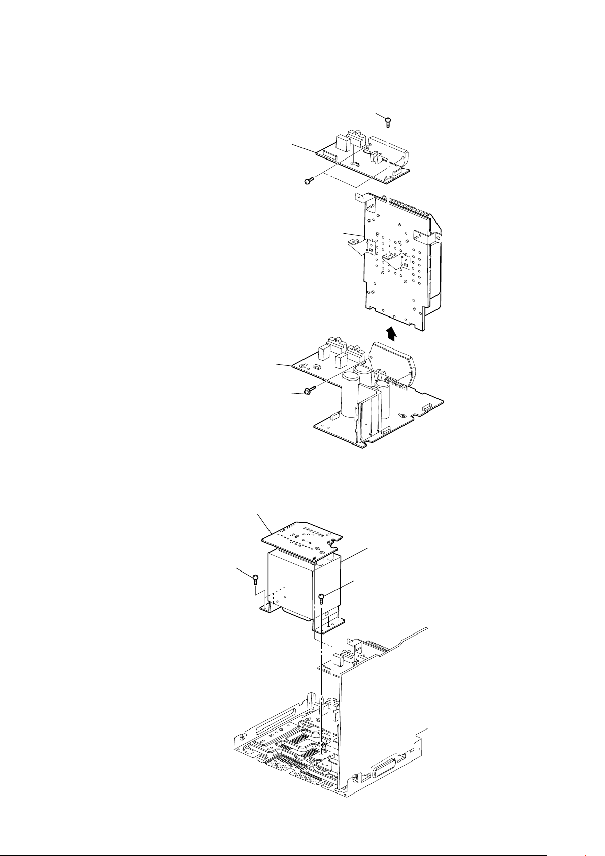
HCD-GTX777/GTX787/GTX888
Ver. 1.1
2-15. BD93 BOARD
Remove the four solders.
BD93
board
wire (flat type) (16 core)
(CN301)
2-16. DRIVER BOARD, SW BOARD, USB R BOARD
DRIVER board
two screws
(+BVTP2.6 (3CR))
USB board
CN704 (2P)
wire (flat type) (5 core)
(CN702)
two screws
(+BVTT (M2.6))
CN703 (4P)
screw
(+BVTT (M2.6))
SW board
20
Page 21
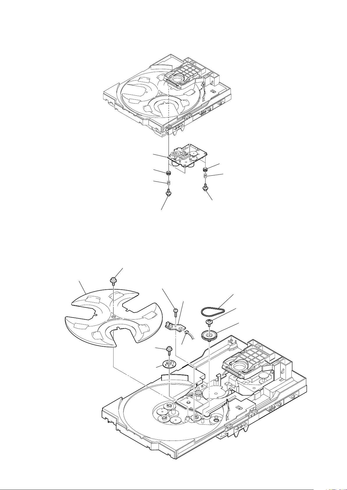
2-17. OPTICAL PICK-UP
optical pick-up
(BU-K6BD93UR)
two insulators
two coil springs
(insulator)
HCD-GTX777/GTX787/GTX888
two insulators
two coil springs
(insulator)
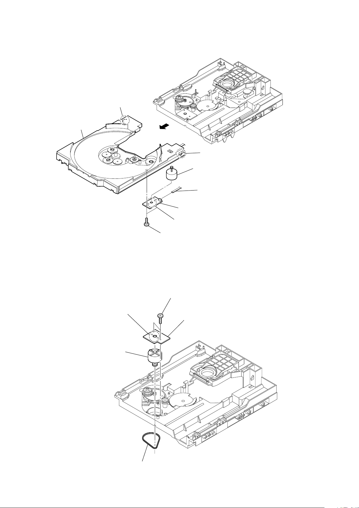
2-18. SENSOR BOARD
t
ray
floating
(+PTPWH M2.6)
floating
(+PTPWH M2.6)
g
screw
(+BTTP (M2.6))
screw
ear (geneva)
one screw
two floating screws
(+PTPWH M2.6)
SENSOR board
CN731
(3P)
two floating screws
(+PTPWH M2.6)
b
elt (table)
floating
(+PTPWH M2.6)
p
ulley (table)
screw
21
Page 22
HCD-GTX777/GTX787/GTX888
2-19. MOTOR (TB) BOARD
stopper
table
2-20. MOTOR (LD) BOARD
Remove the two solderings of motor.
Remove the two solderings of motor.
two screws
(+BTTP (M2.6))
two screws
(+BTTP (M2.6))
stopper
t
able motor assy (M741)
wire (flat type) (5 core)
(CN742)
MOTOR (TB) board
MOTOR (LD) board
22
l
oading motor assy (M751)
b
elt (loading)
Page 23

SECTION 3
TEST MODE
HCD-GTX777/GTX787/GTX888
[GC TEST MODE]
• This mode is used to check the fl uorescent indicator tube, LEDs,
buttons, MASTER VOLUME knob, OPERATION DIAL knob,
model, destination, software version.
Procedure:
1. Press x button, [DELAY] button and [DISC 2] button
simultaneously.
2. All LEDs and segments in fl uorescent indicator tube are lighted
up.
All LEDs are lighted up in red color except for
the LED is lighted up in red and blue color.
3. When you want to enter to the model version and destination
display mode, press [DISC 1] button. The model information
appears on the fl uorescent indicator tube.
4. Each time [DISC 1] button is pressed, the display changes to
display software version and date of the software creation. The
sequence is SC version, GC version, SYS version, CD version,
CDDM version, CDMA version, CDMB version, BDA version,
BDB version, ST version, TC version, TA version, TM version,
MM1 version, MM2 version and MTR version in this order, and
returns to the model version display.
5. Press [DISC 2] button, the key check mode is activated.
6. In the key check mode, the fl uorescent indicator tube displays
“K 0 J0 V0”.
Turn the [OPERATIONAL DIAL] clockwise; “J” value increases
by one. Turn the [OPERATIONAL DIAL] counterclockwise; “J”
value decreases by one. Each time a button is pressed, “K” value
increases. Press other keys on main unit to check whether the
key is detected. However, once a button has been pressed, it is
no longer taken into account.
“V” value increases in the manner of 0, 1, 2, 3 ... if [MASTER
VOLUME] knob is turned clockwise, or it decreases in the manner
of 0, 9, 8, 7 ... if [MASTER VOLUME] knob is turned
counterclockwise.
7. When [DISC SKIP/EX-CHANGE] button is pressed after all LEDs
and segments in fl uorescent indicator tube light up, alternate
segments in fl uorescent indicator tube and LED would light up.
If you press [DISC SKIP/EX-CHANGE] button again, another half
of alternate segments in fl uorescent indicator tube and LEDs
would light up. Press [DISC SKIP/EX-CHANGE] button would
cause all segments in fl uorescent indicator tube and LED turns
off. Pressing [DISC SKIP/EX-CHANGE] button again would cause
all LED and segments lights up.
8. To release from this mode, press three buttons in the same man-
ner as step 1, or disconnect the power cord.
LED where
[MC TEST MODE]
• This mode is used to check operations of the respective sections
of Amplifi er, Tuner and Tape.
Procedure:
• To enter MC Test Mode
1. Press x button, [DELAY] button and [DISC 3] button
simultaneously.
2. The CD ring indicators fl ash on the fl uorescent indicator tube.
The function is changed to VIDEO.
* Check of Amplifi er
1. Press [EQ BAND/MEMORY] button repeatedly until a message
“GEQ MAX” appears on the fl uorescent indicator tube. GEQ
increases to its maximum.
2. Press [EQ BAND/MEMORY] button repeatedly until a message
“GEQ MIN” appears on the fl uorescent indicator tube. GEQ
decreases to its minimum.
3. Press [EQ BAND/MEMORY] button repeatedly until a message
“GEQ FLAT” appears on the fl uorescent indicator tube. GEQ
is set to fl at.
4. When the [MASTER VOLUME] knob is turned clockwise even
slightly, the sound volume increases to its maximum and a message “VOLUME MAX” appears on the fl uorescent indicator
tube.
5. When the [MASTER VOLUME] knob is turned counter-clockwise
even slightly, the sound volume decreases to its minimum and a
message “VOLUME MIN” appears on the fl uorescent indicator
tube.
* Tape function
1. Insert a tape in deck. The function is changed to VIDEO au-
tomatically when the recording is started by pressing [REC TO
TAPE] then press [ENTER] button.
2. During recording, press m button will stop the recording and
the function is changed to TAPE and rewind the tape in Deck
until the recording start position and playback of the tape in
Deck is started.
* To release from MC Test mode
1. To release from this mode, press ?/1 button.
2. The cold reset is enforced at the same time.
[COLD RESET]
• The cold reset clears all data including preset data stored in the
RAM to initial conditions. Execute this mode when returning the
set to the customer.
Procedure:
1. Press x button, [DELAY] button and ?/1 button
simultaneously.
2. The fl uorescent indicator tube becomes blank for while, and the
set is reset.
[VACS ON/OFF]
• This mode is used to switch ON and OFF the VACS (Variable
Attenuation Control System).
Procedure:
1. Press ?/1 button to turn on the system.
2. Press x button and [OPTIONS] button simultaneously. The
message “VACS OFF” or “VACS ON” appears on the fl uorescent
indicator tube.
[TUNER STEP CHANGE]
• The step interval of AM channels can be toggled between 9 kHz
and 10 kHz.
Procedure:
1. Press ?/1 button to turn on the system.
2. Press [TUNER/BAND] button to select the “AM”.
3. Press ?/1 button to turn off the system.
4. Press [ENTER] button and ?/1 button simultaneously. The
system will turn on automatically. The message “AM 9K STEP”
or “AM 10K STEP” appears on the fl uorescent indicator tube
and thus the channel step is changed.
23
Page 24
HCD-GTX777/GTX787/GTX888
[CD SERVICE MODE]
• This mode let you move the CD sled motor freely. Use this mode
when you want to clean the optical pick-up.
Procedure:
1. Press ?/1 button to turn on the system.
2. Select CD function.
3. Press x button, [DELAY] button and [OPEN/CLOSE] button
simultaneously.
4. The CD service mode is activated. The message “SERVICE
MODE” appears on the fl uorescent indicator tube.
5. With the CD in stop status, press M to move the optical pick-
up to outside track, or turn m to move to inside track. The
message “SLED OUT” or “SLED IN” appears on the fl uorescent
indicator tube.
6. To turn on or off the laser, press > button. The message “LD
ON” or “LD OFF” appears on the fl uorescent indicator tube.
7. To release from this mode, press ?/1 button to turn off the
system.
[CD AGING MODE]
• This mode can be used for operation check of CD section. If
an error occurs, the aging operation would stops and the status
is displayed. If there were no error occurs, the aging operation
would continue repeatedly.
Procedure:
1. Press ?/1 button to turn on the system.
2. Select CD function.
3. Load three discs on disc tray.
4. Press [PLAY MODE/TUNING MODE] button on the remote con-
trol repeatedly to select the “ALL DISCS” mode, and press the
[REPEAT/FM MODE] button on the remode control repeatedly
to select repeat mode off.
5. Press x button, [DELAY] button and [DISC SKIP/EX-CHANGE]
button simultaneously.
6. Aging operation is started.
7. To release from this mode, press ?/1 button or disconnect the
power cord to turn the power OFF.
• Aging mode sequence:
START
DISC CHUCKING
TOC READING
PLAY FIRST TRACK FOR 2
SECONDS
PLAY LAST TRACK FOR 2
SECONDS
EX-CHANGE OPEN/CLOSE
OPEN THE DISC TRAY
DISC SKIP
CLOSE THE DISC TRAY
CHANGE THE NEXT DISC
24
Page 25
HCD-GTX777/GTX787/GTX888
[CD ERROR CODE MODE]
• Display the CD error code when an error occurred.
Procedure:
1. Press x button, [DELAY] button and [DISC 1] button
simultaneously to enter the error code display mode.
2. The fl uorescent indicator tube display the number of total error.
3. Each time m button and M button are turned, display
change as below.
DISPLAY OF
TOTAL ERROR
.N
.
.
BUTTON
DISPLAY OF
MECHANICAL
ERRORS
.N
BUTTON
DISPLAY OF
NO DISC
ERRORS
BUTTON
.
BUTTON
.
4. To clear the error record, operate the cold reset. (Refer to the
“MC COLD RESET”.)
5. To release from this mode, press the ?/1 button or disconnect
the power plug to turn the power OFF.
• Display of total error
Em**Ed**
Em** : The number of times for CDM (mechanical) errors.
Ed** : The number of times for BD error (after chucking the
disc.).
• Display of CDM (mechanical) error. It is show with “M” and
11 digit number.
M*$$%%&&0–
000
M* : The number of history error for mechanical. (“0” is
latest one) (Turn > button to display next error.)
$$ : Mechanical errors occur in the operation.
FF : Mechanical error during normal operation.
Other : Mechanical error during initializing operation.
%% : The process when trouble occurs
01 : Process ejecting DISC
02 : Process waiting for inserting DISC
03 : Process sending request to insert a disc to upper
layer.
04 : Process sending request to eject a disc to upper
layer.
05 : Process pulling a DISC in.
06 : Chucking process
07 : Re-chucking process
08 : Process cancelling chucking
&& : The operation when trouble occurs
00 : Waiting for operation.
10/11/12/13: During eject operation
20 : While pulling a disc in
30 : While cancelling chucking
40/41/42/43: During eject operation due to error.
0000 : Not used (Value is fi xed to 0000).
• Display of BD error. It is shown with “D” and 11 digits
number.
D*$$%%&&#–
#00
D* : The number of error history (“0” is latest one)
(Press > button to display next error.)
$$ : The detail of trouble
01 : Can not focus
02 : GFS error
03 : Start-up time over
04 : Continuously out of focus
05 : Q code is not input for certain time
06 : Tracking on is impossible
07 : Blank disc
%% : The process when trouble occurs
01 : While SHIP process is performed
02 : While POWER OFF is processed
03 : While INITIALIZE (POWER ON) is processed.
04 : While oscillation stops
05 : From stopping oscillation to start oscillation
06 : During stop
07 : During STOP operation
08 : While start-up is processed
09 : While TOC reading is processed
0a : During search operation
0b : During PLAY operation
0c : During pause operation
0d : During PLAY manual search operation
0e : During PAUSE manual search operation
&& : Processing operation when trouble occurs
Show each STEP mentioned in %% digits.
## : Disc speed when trouble occurs.
01 : x1 speed
02 : x2 speed (for models which support x2 speed)
04 : x4 speed
00 : Not used (value is fi xed to 00).
25
Page 26

HCD-GTX777/GTX787/GTX888
[CD REPEAT 5 LIMIT OFF MODE]
• The number of repeat for CD playback is 5 times when the repeat mode is “REPEAT ALL”. This mode enables CD to repeat
playback for limitless times.
Procedure:
1. Press ?/1 button to turn on the system.
2. Select CD function.
3. Press [EQ BAND/MEMORY] button, [CD] button and [DISC 1]
button simultaneously to enter the CD repeat 5 limit off mode
and the fl uorescent indicator tube displays “LIMIT OFF”.
• To release from this mode, operate the cold reset.
(Refer to the “MC COLD RESET”.)
[CD SHIP MODE (WITH MEMORY CLEAR)]
• This mode moves the optical pick-up to the position durable to
vibration and clears all data including preset data stored in the
RAM to initial conditions. Use this mode when returning the set
to the customer after repair.
Procedure:
1. Press ?/1 button to turn on the system.
2. Select CD function.
3. Press x button, [SOUND FLASH] button and ?/1 button
simultaneously. The system will turn off automatically.
4. After the “STANDBY” blinking display fi nishes, a message
“MECHA LOCK” is displayed on the fl uorescent indicator tube
and the CD ship mode is set.
5. The Memory is clear after AC Power OFF.
[CD SHIP MODE (WITHOUT MEMORY CLEAR)]
• This mode moves the optical pick-up to the position durable to
vibration. Use this mode when returning the set to the customer
after repair.
Procedure:
1. Press ?/1 button to turn on the system.
2. Select CD function.
3. Press [CD] button and ?/1 button simultaneously. The system
will turn off automatically.
4. After the “STANDBY” blinking display fi nishes, a message
“MECHA LOCK” is displayed on the fl uorescent indicator tube
and the CD ship mode is set.
[CD TRAY LOCK MODE]
• This mode let you lock the disc tray. When this mode is activated,
the disc tray will not open when [OPEN/CLOSE] button or [DISC
SKIP/EX-CHANGE] button is pressed. The message “LOCKED”
will be displayed on the fl uorescent indicator tube.
Procedure:
1. Press ?/1 button to turn on the system.
2. Select CD function.
3. Press x button, [OPEN/CLOSE] button simultaneously and
hold down until “LOCKED” or “UNLOCKED” displayed on
the fl uorescent indicator tube (around 5 seconds).
[TCM OFFLINE MODE]
• This mode is used to prevent the system from turning off automatically when TCM is not connected. Therefore, measurements can
be done even when TCM is not connected during production.
Procedure:
1. When the system is turned off, press [EQ BAND/MEMORY]
button, [TAPE] button and ?/1 button simultaneously. The
system will turn on automatically.
2. The message “TCM OFFLINE” will be displayed on the fl uo-
rescent indicator tube.
[VACS DISPLAY]
• This mode is used to check the VACS level.
Procedure:
1. Press ?/1 button to turn on the system.
2. Press x button, [CHORUS] button and [DISC SKIP/EX-
CHANGE] button simultaneously.
3. The VACS Level Display, the fl uorescent indicator tube displays
“VATB F APC”. “V” represent VACS, A represent VACS level
which is triggered by signal level, “T” represent Thermal VACS
NEO, B represent VACS level which is triggered by temperature,
“F” represent FAN is triggered by software to turn in to high
speed, “AP” represent APVACS (Abuse Protection VACS) and
“C” represent APVACS level which is triggered.
26
Page 27
HCD-GTX777/GTX787/GTX888
[METER SWITCH TOUCH COUNT DISPLAY]
• This mode is used to display the total count of meter pointer
touch initial switch and max switch.
Procedure:
1. Press
button to turn on the system.
2. Press x button, [ENTER] button and [DISPLAY] button
simultaneously.
3. The fl uorescent indicator tube displays “IxxxxxMyyyyy”.
“I” represents the Initial Switch touch.
“xxxxx” represents the total count of Initial Switch touch.
(Maximum Value of “xxxxx” = 65535)
“M” represents the Max Switch touch.
“yyyyy” represents the total count of Max Switch touch.
(Maximum Value of “yyyyy” = 65535)
4 To release from this mode, do step (2) again.
The fl uorescent indicator tube displays “MODE OUT”.
[METER TEST MODE]
• This mode is used to check the meter device.
Procedure:
1. Press button to turn on the system.
2. Press x button, [ENTER] button and [METER MODE] button
simultaneously.
3. Meter Backlight LEDs, Meter Pointer LEDs, Power Illuminator
LEDs and fl uorescent indicator tube are lighted up.
4. When you want to perform count total step from Initial Switch
to Max Switch operation mode, press [>>] button. The meter
pointer will move from Initial Switch to Max Switch and fi nally
move back to the middle position. The total step count information appears on the fl uorescent indicator tube. “xxx STP yy” is
shown.
“xxx” represents the total step.
(Value of “xxx” should between 430 steps to 470 steps)
“yy” represents the status of total step count.
(If total step between 430 steps to 470 steps, “yy” is OK,
else “yy” is NG)
5. When you want to perform count total step from Max Switch
to Initial Switch operation mode, press [<<] button. The meter
pointer will move from Max Switch to Initial Switch and fi nally
move back to the middle position. The total step count information appears on the fl uorescent indicator tube. “xxx STP yy” is
shown.
“xxx” represents the total step.
(Value of “xxx” should between 430 steps to 470 steps)
“yy” represents the status of total step count.
(If total step between 430 steps to 470 steps, “yy” is OK,
else “yy” is NG)
6 To release from this mode, do step (2) again.
The fl uorescent indicator tube displays “TST MODE OUT”.
SECTION 4
MECHANICAL ADJUSTMENTS
Precaution
1. Clean the following parts with a denatured alcohol-moistened
swab:
record/playback heads pinch rollers
erase head rubber belts
capstan idlers
2. Demagnetize the record/playback head with a head demagnetizer.
3. Do not use a magnetized screwdriver for the adjustments.
4. After the adjustments, apply suitable locking compound to the
parts adjusted.
5. The adjustments should be performed with the rated power
supply voltage unless otherwise noted.
Torque Measurement
Mode Torque meter Meter reading
2.9m N • m to 6.9m N • m
FWD CQ-102C 30 to 70 g • cm
(0.42 – 0.97 oz • inch)
FWD 0.15m N • m to 0.59m N • m
back tension CQ-102C 2 to 6 g • cm
(0.03 – 0.08 oz • inch)
2.9m N • m to 6.9m N • m
REV CQ-102RC 30 to 70 g • cm
(0.42 – 0.97 oz • inch)
0.15m N • m to 0.59m N • m
REV
CQ-102RC 2 to 6 g • cm
back tension
4.8m N • m to 16.7m N • m
FF/REW CQ-201B 49 to 170 g • cm
(0.68 – 2.36 oz • inch)
(0.03 – 0.08 oz • inch)
27
Page 28
HCD-GTX777/GTX787/GTX888
ELECTRICAL ADJUSTMENTS
SECTION 5
TUNER SECTION 0 dB = 1 µV
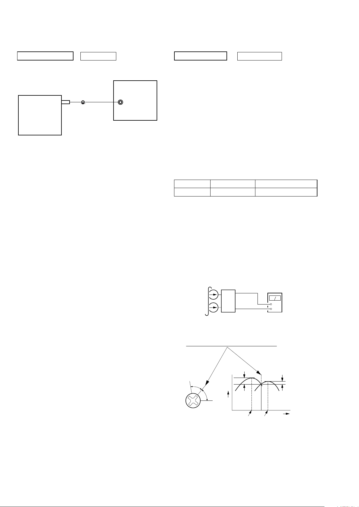
[FM Tune Level Check]
FM signal generator
SET
Procedure:
1. Turn the power on.
2. Input the following signal from Signal Generator to FM antenna input directly.
* Carrier Freq : A = 87.5 MHz, B = 98 MHz, C = 108 MHz
Deviation : 75 kHz
Modulation : 1 kHz
ANT input : 35 dBu (EMF)
Note: Please use 75 ohm “coaxial cable” to connect SG and the set. You
cannot use video cable for checking.
Please use SG whose output impedance is 75 ohm.
3. Set to FM tuner function and tune A, B and C signals.
4. Confi rm “TUNED” is lit on the display for A, B and C signals.
The mark of “TUNED” means “The selected station signal is received in good condition.”
OUT (75 7)
DECK SECTION 0 dB = 0.775 V
1. Demagnetize the record/playback head with a head
demagnetizer.
2. Do not use a magnetized screwdriver for the adjustments.
3. After the adjustments, apply suitable locking compound to the
parts adjust.
4. The adjustments should be performed with the rated power
supply voltage unless otherwise noted.
5. The adjustments should be performed in the order given in this
service manual. (As a general rule, playback circuit adjustment should be completed before performing recording circuit
adjustment.)
6. The adjustments should be performed for both L-CH and RCH.
7. Switches and controls should be set as follows unless otherwise
specifi ed.
• Test Tape
Tape Signal Used for
P-4-A100 10 kHz, –10 dB Azimuth Adjustment
[RECORD/PLAYBACK HEAD AZIMUTH
ADJUST-MENT]
Note: Perform this adjustments for Single deck
Procedure:
1. Mode: Playback
test tape
P-4-A100
(10 kHz, –10 dB)
(L-CH & R-CH)
set
level meter
+
–
2. Turn the adjustment screw and check output peaks. If the peaks
do not match for L-CH and R-CH, turn the adjustment screw
so that outputs match within 1dB of peak.
output
level
within
1dB
L-CH
peak
R-CH
peak
within
1dB
screw
position
L-CH
peak
screw
position
R-CH
peak
28
Page 29
HCD-GTX777/GTX787/GTX888
3. Mode: Playback
test tape
P-4-A100
(10 kHz, –10 dB)
L-CH
R-CH
waveform of oscilloscope
in phase
L
R
45o 90 o 135o 180 o
good
oscilloscope
V
wrong
H
4. After the adjustments, apply suitable locking compound to
the parts adjusted.
Adjustment Location: Playback Head (Deck).
CD SECTION
[TEST DISC LIST]
Use the following test disc on test mode.
• CD: YEDS-18 (PART No. 3-702-101-01)
or
PATD-012 (PART No. 4-225-203-01)
Note:
1. CD Block is basically designed to operate without adjustment.
Therefore, check each item in order given.
2. Use YEDS-18 (3-702-101-01) unless otherwise indicated.
3. Use an oscilloscope with more than 10MW impedance.
4. Clean the object lens by an applicator with neutral detergent
when the signal level is low than specifi ed value with the
following checks.
[S-CURVE CHECK]
oscilloscope
BD93 board
TP106(FE)
TP124(VC)
Procedure :
1. Connect an oscilloscope to TP106 (FE) and TP124 (VC).
2. Turn the power on.
3. Load a disc (YEDS-18) and actuate the focus search. (In
consequence of open and close the disc tray, actuate the focus
search)
4. Confi rm that the oscilloscope waveform (S-curve) is symmetrical
between A and B and confi rm peak to peak level within 3 ± 0.5
Vp-p.
+
–
forwa rd
S-curve waveform
symmetry
A
within 3
B
±
0.5Vp-p
Note: • Try to measure several times to make sure that the ratio
of A : B or B : A is more than 10 : 7.
• Take sweep time as long as possible and light up the
brightness to obtain best waveform.
29
Page 30
HCD-GTX777/GTX787/GTX888
[RF LEVEL CHECK]
oscilloscope
BD93 board
TP123(RFO)
TP124(VC)
Procedure :
1. Connect an oscilloscope to TP123 (RFO) and TP124 (VC).
2. Turn the power on.
3. Load a disc (YEDS-18) and playback.
4. Confi rm that oscilloscope waveform is clear and check if RF
signal level is correct or not.
Note: Clear RF signal waveform means that the shape “ ◊ ” can
be clearly distinguished at the center of the waveform.
+
–
RF signal waveform
Connecting Location: CD board
– BD93 Board (SIDE B) –
TP124
(VC)
(FE)
IC101
25
51
50
26
TP123
(RFO)
75
76
100
1
TP106
VOLT/DIV: 200 mV
TIME/DIV: 500 ns
level: 1.3
±
0.3 Vp-p
30
Page 31

SECTION 6
DIAGRAMS
6-1. BLOCK DIAGRAM — RF/SERVO SECTION —
HCD-GTX777/GTX787/GTX888
DETECTOR
OPTICAL PICK-UP
BLOCK
(KSM-213DCP)
LASER
DIODE
2AXIS
DEVICE
FOCUS/
TRACKING
COIL
M402
(SLED)
M401
(SPINDLE)
CD+1.5V REG
IC201
A
B
C
D
F
E
VREF
VC
AUTOMATIC
LD
PD
FCS+
FCS–
TRK+
TRK–
M
M
M
M
POWER
CONTROL
Q301
F+
F–
T+
T–
SL–
SL+
SP+
SP–
VM+7V
95
FNI1
97
FPI1
94
FNI2
96
FPI2
98
TPI
100
TNI
11
VREF
77
PVREF
84
VRO
91
LD0
92
MDI
FOCUS/TRACKING COIL DRIVER,
SPINDLE, SLED MOTOR DRIVER
26
27
18
17
21
•
22
11
12
2
1
IC401
FOCUS COIL
DRIVE
TRACKING COIL
DRIVE
SLED MOTOR
DRIVE
SPINDLE MOTOR
DRIVE
CD RF AMP,
FOCUS/TRACKING ERROR AMP,
DIGITAL SIGNAL PROCESSOR,
DIGITAL SERVO PROCESSOR,
DIGITAL FILTER,D/A CONVERTER
24
20
9
3
23
BIAS
MUTE
7
IC101
FOO
TRO
FMO
DMO
VREF
X102
16.934MHz
FOO
TRO
FMO
DMO
30
LO
27
RO
BCK(PO8)
PIO3
PIO1
BUS3 (SI)
BUS1
BUS0
PIO0
47
63
51
49
41
40
39
38
48
AOUT2(PO5)
BUS2 (SO)
9
FOa
10
TRa
12
FMO
13
DND
XI
23
XO
24
CD LCH
CD RCH
DATA
CLK
GATE
ST REQ
BUS0
BUS1
BUS2
BUS3
REQ
CCE
BUCK
DVDD+3.3VCD+1.5V
MAIN
A
SECTION
• Signal Path
: CD PLAY
: DIGITAL
SELECT
SWITCH
Q108
: USB
SELECT SWITCH
IC200
112
SELECT
10
3B
11
3A
14
4A
15
ST
3
1B
2
1A
6
2B
5
2A
12
4Y
9
3Y
4
1Y
7
2Y
B
USB
SECTION
SELECT SWITCH
IC202
10
4O/I
11
4I/O
3O/I
9
8
3I/O
2O/I
3
4
2I/O
2
1O/I
1
1I/O
SELECT SWITCH
IC201
10
4O/I
11
4I/O
3O/I
9
8
3I/O
2O/I
3
4
2I/O
4C
6
3C
5
2C
13
1C
4C
12
6
3C
5
2C
MAIN
J
SECTION
HCD-GTX777/GTX787/GTX888
R-IN
L-IN
SECTION
USB
IC501
A/D CONVERTER
1
2
A IN
K
2
1O/I
1
IC502
BUFFER
10
12
6
3
11
4
7
9
66
BCKI(P15)
67
LRCKI(P16)
AIN(P14)
65
CCE
BUCK
RST
SBSY
43
42
37
54
SYSTEM CONTROL
IC401 (1/6)
2 79
RST
19
SBSY
3
M-MUTE
BUS3
BUS2
BUS1
BUS0
SEL SW
BUCK
CCE
REQ
80
81
82
7
6
5
1
1I/O
13
1C
31 31
Page 32

HCD-GTX777/GTX787/GTX888
6-2. BLOCK DIAGRAM — TAPE/TUNER SECTION —
IC301
PB AMP
TC-PB-L
C
MAIN
SECTION
REC/PB
HEAD
L – CH
R – CH
ERASE
HEAD
FM 75
COAXIAL
DECK
TAP E
MECHANISM
BLOCK
REC(FWD)
B SHUT
BHALF
BTRGM+
CAP M+
R-CH
R-CH
FM/AM TUNER UNIT
FM ANT
Q401,403
TU901
Q456
T001
ST-R
Q405
MUTE
ST-L
REC
BIAS OSC
Q453
R-CH
Q407
IC401
REC EQ
+9V
Q454,455
A TRIGGER DRIVE
Q213,215
CAPSTAN MOTOR DRIVE
Q212,214
ST-L
E
MAIN
SECTION
+9V
MUTE SW
Q409,410
MUTE SW
Q408,411
SYSTEM CONTROL
(TAPE MECHANISM CONTROL)
IC401 (2/6)
61
REC-MUTE
TBL SENS
REC BIAS
63
47
B-SHUT
B-HALF
83
60
TC-RELAY
39
B-TRIG
CAPM-+
18
OPENSW
REC-OUT-L
25 3
TM-F
32
TM-R
21
E-1
22
E-2
27
E-3
23
24
REC-OUT-L
TABLE ADDRESS SENSOR
Q731
FIN
7
RIN
9
MAIN
D
SECTION
IC731
4
TBL MOTOR DRIVER
IC712
MOTOR
DRIVE
ROTARY ENCODER
ADDRESS DETECT
S751
OPEN/CLOSE
DETECT
1
2
OUT2
OUT1
RE701
DISC TRAY
M+9V
2
4
M741
M
(TABLE)
AM
ANTENNA
HCD-GTX777/GTX787/GTX888
AM ANT
AM ANT
ST-DIN/MC-DOUT
ST-DOUT
ST-CLK
ST-CE
ST-DIN/MC-OUT
68
SY-DOUT/MC-DIN
70
69
ST-CLK
ST-CE
67
• R-CH is omitted due to same as L-CH.
• Signal Path
: AUDIO
: TUNER
: TAPE PLAY (DECK A)
: TAPE PLAY (DECK B)
: RECORD (DECK B)
3232
Page 33

6-3. BLOCK DIAGRAM — MAIN SECTION —
14
CLOCK
RV1150
MIC
LEVEL
DIGITAL DELAY
IC501
LPF2OUT
OP2OUT
LPF1OUT
AUDIO
IN
VIDEO
IN
J1100
(1/2)
MIC
MIC AMP
IC1100
(1/2)
J101
L
R
L
R
RCH
RCH
MULTIPLEXER
IC500
11
A
10
B
C
9
COM
3
LPF2IN
OP2IN
MIC AMP
IC1100
(2/2)
9
10
11
12
3
Q500
Q501
TAPE/TUNER
SECTION
TAPE/TUNER
SECTION
X
E
XC
Q505
BUFFER
Q503
ST L
TC PB L
Q555
3
5
RF/SERVO
SECTION
MIXER
IC502
XA
1
7
CD LCH
CD RCH
RCH
INPUT SELECT SWITCH
IC50
46
MIC
43
ST-L
41
TAPE-L
42
AUX-L
45
VIDEO-L
38
OUTL
5
OUTR
AGCOUTL
39
GAMEL
44
CD-L
46
CD-R
SA2
RECB1
OUTL
BB A1
BB B1
HCD-GTX777/GTX787/GTX888
9
METER LEVEL
37
IC51
26
MUTE
Q51
25
27
28
DBFB
SWITCH
Q52
REC OUT L
F–L
GTX888 GTX888 GTX888
DBFB F/B
TAPE/TUNER
X
D
AMP/SUBWOOFER
X
F
SECTION
IC2030 IC2031
AMP/SUBWOOFER
X
I
SECTION
A+9V
AMP
Q100,101
SECTION
D206,207
D+4V REG
Q202
MUTE
Q53
LINE MUTE
Q303
L+R
SW OUT
GTX888
CN200
D-LIGHT
SYNC OUT
AMP/SUBWOOFER
X
H
SECTION
76 77 78
S0S1S2
EFFECTOR
LPF1IN
2
BUFFER
Q504
ND900
41
CTRL
8
+VG
D+3.3V
40
3
CTRL
1
SYSTEM CONTROL
IC401 (3/6)
129
10
Q900
CLK BK DATA
31
CLOCK
282633
LATCH
DATA
21
22
3
7
5
36
IC100
AMP
1531113
VF+
VF-
R-IN
1
X
L-IN
J
RF/SERVO
SECTION
57 58 94
DATA CLK LINE
M61529
SW IN
LEVEL
SW ON
100
LED
72
METER
LEVEL
7
• R-CH is omitted due to same as L-CH.
• Signal Path
: AUDIO
: TUNER
: TAPE PLAY (DECK A)
: TAPE PLAY (DECK B)
: MIC
51
MUTE
CN201
SWITCH
CONTROL
HCD-GTX777/GTX787/GTX888
33 33
Page 34

HCD-GTX777/GTX787/GTX888
6-4. BLOCK DIAGRAM — USB SECTION —
RF/SERVO
SECTION
CN952
(USB)
B
USB CONTROL
IC901
VBUS
POWER ON/OFF
SWITCH
OUT
VBUS
1
D–
D+
GND
4
BUS3
BUS2
BUS1
BUS0
IC915
FLG
VBUS+5V
IN
45
P75/USBOC
3
EN
1
77
P76/USBPON
78
80
D–
D+
79
PF1/RXDODATA
85
PF2/SCLK0/CTSO/CLK/TB0OUT0CLK
86
PN5/HSS1/SCL1GATE
94
PG2ST REQ
97
PN3/HSCLKBCK IN
92
P83/CS3/WAIT/TA5OUTLRCKIN
71
P64/A20
58
57
P63/A19
P62/A18
56
P61/A17
55
P71/SRWR
P72/SRLLB
P73/SRLUB
18
P00/D0
I
I
25
P07/D7
•
28
P10/D8
I
I
35
P17/D15
37
P41/A1
I
I
43
P47/A7
•
46
P50/A8
I
I
54
P60/A16
64 41
P70/RD
65
66 39
67
70 6
P82/CS2
7
I
10
•
13
I
16
•
29
I
32
•
35
I
38
44
I
42
•
27
I
24
•
21
I
18
•
5
I
1
17
40
I/O0
I/O3
I/O4
I/O7
I/O8
I/O11
I/O12
I/O15
A0
A2
A3
A6
A7
A10
A11
A15
OE
WE
LB
UB
CE
S-RAM
IC921
I
I
I
I
I
I
I
I
• Signal Path
SYSTEM CONTROL
: DIGITAL
: USB
IC401 (4/6)
RF/SERVO
SECTION
K
PG3REQ
96
P66/A22CCE
60
P65/A21BUCK
59
PF4/RXD1/SPDI
PN4/HSS0/SDA1A IN
93
PF3/TXD1/SPD0
1 37
RESET
2
PC0/INT0
84 34
PF0/TXD0
88
87
75
X1
X2
X901
9kHz
73
USBRST
38
USB SERIAL RTSO
USB SERIAL CTSO
35
USB SERIAL TXDO
36
USB SERIAL RXDO
HCD-GTX777/GTX787/GTX888
3434
Page 35

6-5. BLOCK DIAGRAM — AMP/SUBWOOFER SECTION —
HCD-GTX777/GTX787/GTX888
MAIN
SECTION
MAIN
SECTION
POWER AMP
IC601: GTX888
IC602: GTX777/GTX787
F-L
F
F-R
18 11
14
12
MUTING
Q631-633
-VH
GTX888
10
8
9
+ + +
I
THERMAL
DETECT
Q671,672
DBFB F/B
OVER LOAD
TH629
DETECT
Q681,682
D601
OVER CURRENT
PROTECTOR
Q621,622
RY646
RELAY DRIVE
Q644, 647
OVERLOAD
DETECT
SWITCH
Q611,612
UNREG 9V
FAN DETECT
Q111,112
FAN MOTOR
DRIVE
Q111
FAN MOTOR
DRIVE
Q205,206
M891
DC FAN
M892
DC FAN
GTX888
RY665
RELAY DRIVE
Q666
GTX777
J1101
PHONES
+
L
-
+
R
-
+
L
-
+
R
-
TM600
FRONT SPEAKER
GTX888/GTX777
TM601
SURROUND SPEAKER
• R-CH is omitted due to same as L-CH.
• SIGNAL PATH
: AUDIO
GTX888
MAIN
SECTION
OVERLOAD
+VL
–VL
DETECT
Q800
OVERLOAD
93
THERMAL VACS
DETECT
Q850
TH630
RY862
RELAY
DRIVE
Q814
AC CUT
DETECT
Q815
EXCEPT MX
55
PROTECTOR
52
FRONT RELAY
MX
54
SW-RELAY
SUBWOOFER POWER AMP
IC800
+RE1
4
5
L
15
IN1
STK MUTE
R
11
IN2
13
ST BY
SW OUT
H
49
–RE1
+RE2
–RE2
+VCC
–VCC
6
7
3
2
FAN DETECT
Q221,222
FAN CONTROL
SYSTEM CONTROL
IC401 (5/6)
SWITCH
Q220
56
FAN HI SPEED
HI SPEED
SWITCH
Q223
50
FAN ON
EEPROM
IC675
5 6
97
EEP_SDA
53 66
95
EEP_SCA
GTX888
+
L
-
+
R
-
HP DET
LINK RELAY
TB001
SUB WOOFER
OUT
HCD-GTX777/GTX787/GTX888
35 35
Page 36

HCD-GTX777/GTX787/GTX888
6-6. BLOCK DIAGRAM — DISPLAY/POWER SECTION —
LED +9V
MOTOR(LD)
M751
LED +9V
14
IND1-4
|
17
12
D914,915
D1000
D1003
LED SWITCH
Q904,209
7
8
9
6
LATCH
IC902
3
4
5
13
10
MOTOR
9
M
DRIVE
IC701
D920-925
D908-913
7
12
13
|
16
6
|
11
REMOTE CONTROL
SIGNAL RECEIVER
IC1101
OPERATION
LATCH
IC900
S936
DIAL
S935
MASTER
VOLUME
18
3
4
5
ROTARY
ENCODER
ROTARY
ENCODER
NO111
(FOR CHECK)
IIC-DATA
IIC-CLK
S914-919
S901-911,920-925,
S937,950
S926-928,
S913,941
GTX888
S951-953
S940
S939
GTX727,787
32.768kHz
MOTOR
2
|
510
DRIVE
IC001
7
OUT1-4
|
D011-014
S031
LED +9V MASTER LED CONTROL
+9V SW
Q903
65 METER POSITION SW
43 LED DRIVER-DATA
44 LED DRIVER-CLOCK
42 LED DRIVER-LATCH
4 SIRCS
88 OP DIAL
87 MASTER VOL
30
IIC-DATA
29
IIC-CLK
84 ADKEY0
85 ADKEY1
86 ADKEY2
73 DISPLAY/POWER KEY
15 X-IN
13 X-OUT
10 XC-IN
5MHz
X401
X402
11 XC-OUT
+9V
D906
LED +9V
STBY LED
SYSTEM CONTROL
IC401 (6/6)
LED
SWITCHI
Q902
D905
46
PT1201
POWER
RY1200
TRANSFORMER
VL
VL
GND
VH
VH
VP
D1292
RECT
VF
VF
AC3
AC3
AEP
AC IN
AC IN
EXCEPT AEP, MX
230-240V
220V
120V/127V
S1200
VOLTAGE
SELECT
AC IN
MX
DVSS +3.3V
D +3.3V
90OVER VOLTAGE
48STBY-RELAY
12RESET
20AC-CUT
CN112
(3/3)
RESET
SWITCH
Q207
3.3V REG
IC204
RESET
(FOR CHECK)
USB +5V
LED +9V
LEVEL
DETECT
Q627,628
DC FAN
M +9V
ST +9V
USB+5V REG
IC203
A+9V
M893
EVER +10V
D1210
FAN MOTOR
DRIVE
Q205,206
+9V REG
IC206
+9V REG
IC209
USB+9V REG
IC205
+9V REG
IC207
UNREG
D227,228
D1201
D1202
FRUORESCENT
+3.3V REG
Q209-211
+VL
–VL
+VH
–VH
+ VG
(+32V)
ND900
VACUUM
DISPLAY
RECT
D622
RECT
D621
+ 33V
REGULATOR
Q1291
D1291
VF+
VF-
RECT
D114
POWER ON/OFF
RELAY DRIVE
EVER 3.3V
+4V REG
IC208
Q1211
PT1200
8
6
SUB POWER
TRANSFORMER
F1261
F1251
F1241
F1271
R1292
D1294
D1295
F1281
Q208
HCD-GTX777/GTX787/GTX888
3636
Page 37

6-7. CIRCUIT BOARDS LOCATION
HCD-GTX777/GTX787/GTX888
MOTOR (LD) board
USB R board
PANEL FUNCTION board
ILLUMINATION
METER DISPLAY board
USB CONNECTOR board
board
JOG board
LED board
SENSOR board
BD93 board
SW board
MOTOR (TB) board
TC board
DRIVER (F) board
MAIN board
MIC board
SUB TRANS board
CD-SW board
TRANS board
TUNER PACK
SUBWOOFER board
POWER board
37
Page 38

HCD-GTX777/GTX787/GTX888
• Note For Printed Wiring Boards And Schematic Diagrams
Note on Printed Wiring Board:
• X : parts extracted from the component side.
• Y : parts extracted from the conductor side.
• : Pattern from the side which enables seeing.
(The other layer’s patterns are not indicated.)
Caution:
Pattern face side: Parts on the pattern face side seen from
(Conductor Side) the pattern face are indicated.
Parts face side: Parts on the parts face side seen from
(Component Side) the parts face are indicated.
• Indication of transistor.
C
Q
B
B
B
These are omitted.
E
Q
CE
These are omitted.
Q
CE
These are omitted.
UNLEADED SOLDER
Boards requiring use of unleaded solder are printed with the lead
free mark (LF) indicating the solder contains no lead.
(Caution: Some printed circuit boards may not come printed with
the lead free mark due to their particular size)
: LEAD FREE MARK
Unleaded solder has the following characteristics.
• Unleaded solder melts at a temperature about 40 °C higher than
ordinary solder.
Ordinary soldering irons can be used but the iron tip has to be
applied to the solder joint for a slightly longer time.
Soldering irons using a temperature regulator should be set to
about 350 °C.
Caution: The printed pattern (copper foil) may peel away if the
heated tip is applied for too long, so be careful!
• Strong viscosity
Unleaded solder is more viscous (sticky, less prone to fl ow) than
ordinary solder so use caution not to let solder bridges occur such
as on IC pins, etc.
• Usable with ordinary solder
It is best to use only unleaded solder but unleaded solder may also
be added to ordinary solder.
Note on Schematic Diagram:
• All capacitors are in µF unless otherwise noted. (p: pF)
50 WV or less are not indicated except for electrolytics
and tantalums.
• All resistors are in Ω and 1/
specifi ed.
• 2 : nonfl ammable resistor.
• C : panel designation.
Note: The components identifi ed by mark 0 or dotted line
with mark 0 are critical for safety.
Replace only with part number specifi ed.
• A : B+ Line.
• B : B– Line.
• Voltage and waveforms are dc with respect to ground
under no-signal (detuned) conditions.
• BD93 and Driver sections.
no mark : CD PLAY
• Except BD93 and Driver sections.
no mark : FM
( ) : CD PLAY
< > : TAPE PLAY
[ ] : TAPE REC
∗ : Impossible to measure
• Voltages are taken with a VOM (Input impedance 10
MΩ).
Voltage variations may be noted due to normal production
tolerances.
• Waveforms are taken with a oscilloscope.
Voltage variations may be noted due to normal production
tolerances.
• Circled numbers refer to waveforms.
• Signal path.
F : AUDIO
f : TUNER
E : TAPE PLAY
G : TAPE REC
N : MIC
J : CD PLAY
c : DIGITAL
I : USB
• Abbreviation
E2 : 120V AC area in E model
E3 : Middle Easten, African and Indian model
E51 : Chilean and Peruvian model
AR : Argentina model
AUS : Australian model
MX : Mexican model
4
W or less unless otherwise
38
Page 39

• Waveforms
HCD-GTX777/GTX787/GTX888
— BD93 BOARD — (CD PLAY)
IC101 (FEI)
Approx.
200 mVp-p
100 mV/DIV, 5 msec/DIV
IC101 (TEI)
Approx.
200 mVp-p
100 mV/DIV, 0.2 msec/DIV
IC101 XG (XO)
3.36Vp-p
— MAIN BOARD —
IC401 R (XC-IN)
1 Vp-p
32.768 kHz
0.5 V/DIV, 0.1 sec/DIV
IC401 RH (X-IN)
1.5 Vp-p
5 MHz
1 V/DIV, 0.1 sec/DIV
27 MHz
1 V/DIV, 0.1 sec/DIV
IC101 PH(FNI1(A))
50 mV/DIV, 0.1 sec/DIV
Approx.
504 mVp-p
— USB BOARD —
1 IC901 ug
1 V/DIV, 0.1 μsec/DIV
(X1)
9 MHz
1.4 Vp-p
HCD-GTX777/GTX787/GTX888
39 39
Page 40

HCD-GTX777/GTX787/GTX888
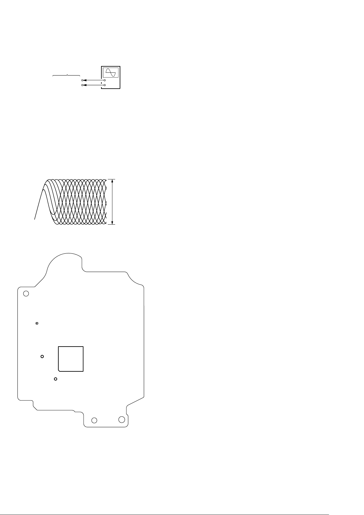
6-8. PRINTED WIRING BOARD — BD93 BOARD — • Refer to page 37 for Circuit Boards Location. : Uses unleaded solder.
12345678 91011 141512 13
A
B
C
D
E
F
G
H
BD93 BOARD (SIDE A) BD93 BOARD (SIDE B)
(SPINDLE)
IC201
C206
135
4
C205
R201
C218
C217
1
1
R2
C207
C201
C401
R212
C204
R214
5
1
C1
R213
C202
C405
R155
X102
R120
C108
10
C1
R104
R415
C132
C153
C11
R114
C102
R512
R503
R514
IC501
R505
C501
C106
C306
C504
C507
C502
R508
C123
C145
C146
C506
C125
C124
R151
R502
C144
C505
C122
C143
C509
R144
C147
C148
C149
C140
R510
C141
R142
C142
C150
R513
R143
C138
C139
8
1
1
C
R509
R139
R140
C100
CN301
R51
1
IC502
C508
C107
2
C101
C309
C105
C104
E
R304
Q301
R303
C307
R302
R301
11
1-875-864-
(11)
OPTICAL
PICK-UP
BLOCK
(KSM-213DCP)
M401
C510
C511
R134
C137
17
1
C
R136
R135
R129
R130
C427
R159
C136
R128
C119
C120
M
R160
R161
R109
IC101
C103
C113
C127
C126
R101
R102
8
11
R
C301
R414
R108
C128
C303
R402
R105
C130
C302
C109
16
1
C
R106
IC401
R121
C133
10
1
R
R153
R154
C404
R216
1
11
R
R405
C403
M402
(SLED)
M
R224
R408
R225
R210
R209
R218
2
1
1
R
R220
R206
R219
R221
R156
R202
R157
R205
R208
R207
R222
C152
R204
R223
C151
R226
R203
CN201
A
MAIN BOARD
CN430
(Page 44)
11
1-875-864-
(11)
I
J
HCD-GTX777/GTX787/GTX888
• Semiconductor Location
Ref. No. Location
IC101
IC201
IC401
IC501
IC502
Q301
E-11
F-2
D-12
C-7
C-6
G-5
4040
Page 41

• Refer to page 39 for Waveforms.
6-9. SCHEMATIC DIAGRAM — BD93 BOARD — • Refer to page 67 IC Block Diagrams.
1234567891011 141512 13
A
BD93 BOARD
B
C136
47p
1k
R139
47k
4.7k
C
D
E
F
OPTICAL
PICK-UP
BLOCK
(KSM-213DCP)
CN301
R142
R143
22k
16P
E
TP305
D
TP304
A
TP301
B
TP302
C
TP303
F
TP306
-
F-
T
F+
T+
11
TP309
TP310
TP3
TP308
0.1
C301
10
C302
TP307
TP313
Q301
AUTOMATIC POWER CONTROL
10
C303
LD
PD
TP314
IOP1
TP315
IOP2
Q301
2SA2119K
C306
R303
2.2
R304
2.2
3.1
1.8
10V
100
C307
1
R301
100k
2.4
R302
0
C309
0.001
TP312
APC
0.1
0.01
C100
C139
C140
10V
C106
100
TP124
0.1
C105
C104
0.1
C148
47k
0.01
470p
C137
C138
3.3
1.6
1.0
TP120
0.01
C141
0.0022
0.1
C142
C143
C144
47p
C150
1.6
1.6
1.6
TP121
TP122
1.7
1.6
R144
22k
1.5
0.01
C146
470p
1.5
1.6
0.1
0.01
C145
1.6
TP123
1.6
3.3
0.1
C147
C149
22p
CH
3.2
0.1
1.6
1.6
1.6
1.6
1.6
1.9
0.001
1.6
R129
R140
R130
22k
0
470k
R136
R134
1M
R135
1.5
1.6
1.6
4
1.6
0.8
0.7
0.022
C118
0.01
TP105
C117
G
TRK
TP102
FCS
TP101
H
R402
2.2k
C405
0.1
3.3
3.4
1.5
1.5
7.4
R405
10k
C403
C404
0.1
0.1
7.4
1.6
3.5
3.5
C107
0.1
470k
R128
0.1
2
1
1
C
3.3
1.50000
FOCUS/TRACKING ERROR AMP,
DIGITAL FILTER,D/A CONVERTER
1
2
1.6
1.6
1.6
3.3
TP107
0.022
TP106
C11 9
C120
0.01
C101
0.1
100
100
100
R108
0
(FERRITE)
R160
R161
R159
R109
100
1.5
IC101
DIGITAL SIGNAL PROCESSOR,
DIGITAL SERVO PROCESSOR,
IC101
TC94A70FG-101
1.6
1.6
1.6
1.6
1.6
1.3
3.3
TP110
0
220
TP111
TP109
TP108
C122
470p
C124
0.0047
0.1
R101
R151
0.1
C126
C103
C102
0.1
470p
C123
C125
0.0047
100k
R118
3.303.3
1.5
0.0022
C127
0.1
C113
HCD-GTX777/GTX787/GTX888
Ver. 1.1
R510
TP508
LRCK
TP507
BCK
0
0
TP506
AIN
0
IC B/D
3.3
IC502
TC74VHC157FT (EKJ)
C508
R513
TP116
PDN
0.1
0.1
C153
TP119
TP118
TP117
TP125
0
0
3.3
3.3
3.3
TP113
TP112
R102
10k
C108
10k
R114
0.1
3.3
0.3
0
0.1
0.1
0.1
0.1
0.1
0
0.1
3.3
3.3
0.1
0.1
0.1
3.3
0
1.5
1.5
3.3
1.7
1.7
3.3
R105
X102
16.934MHz
C132
1.7
3.3
1k
C130
5P
0.1
3
1.5
1.4
5P
C128
R120
R121
MCLK
TP126
R111
100
R110
0.1
C110
1M
R153
C115
22
47
R155
C116
1M
R154
1k
R106
0
R104
1k
IC502
BUFFER
0
0
0
R511
0
0
0
R512
0
F
0.1
100
R509
100k
100
C133
0.1
1
2
1
R
100
10k
C109
0.1
6.3V
0.1
TP226
A3.3V
C511
0.1
1k
C510
0.1
1k
0
47k
R514
R505
R224
100
R216
100
100
R213
100
R214
R212
100
R218
100k
100k
R219
R220
100k
100k
R221
100k
R222
100k
R223
IC201
TK63115SCL-G@GT
1.5
1
TP224
C207
C151
0.0022
100
R157
R156
100
C201
C205
100
0.1
10V
R201
TP225
D3.3V
C202
100
10V
0
0
R202
C204
0.1
47k
47k
R502
R503
C152
IC201
+1.5V REG
IC B/D
A/D CONVERTER
0
0
0
0
0
3.3
3.3
0
R209
100
3.3
3.3
0.0022
IC B/D
IC501
IC501
AK5358AET-E2
R225
R210
R208
R207
R206
R205
R204
R203
1
C206
0.1
C507
TP502
3.3
C506
TP501
0.1
C505
2.2
47k
R508
C218
0.1
C217
0.1
C509
0.1
TP227
TP228
TP201
TP202
TP203
TP204
TP205
TP206
TP207
TP208
TP209
TP210
TP211
TP212
TP213
TP214
TP215
TP216
TP217
TP218
TP219
TP220
TP221
TP223
TP222
TP231
TP230
TP229
10V
100
C504
CN201
31P
A
MAIN BOARD
(3/4)
CN430
(Page 47)
C502
10
16V
R211
100
5.1
0
0
0
0
C501
16V
10
100k
100
R226
100k
100
100
100
100
100
100
I
M401
(SPIDLE)
J
M402
(SLED)
HCD-GTX777/GTX787/GTX888
TP407
TP408
TP409
TP410
SP+
IC401
FOCUS/TRAKING COIL DRIVE,
IC B/D
SLED/SPINDLE MOTRO DRIVE
IC401
BA5826SFP-E2
3.0
3.8
1.4
7.2
3.2
R414
SP-
SL+
SL-
4.7k
1.6
3.2
3.7
R408
2.2k
47k
R415
TP104
SPDL
SLED
TP103
C401
220
10V
41 41
Page 42

HCD-GTX777/GTX787/GTX888
6-10. PRINTED WIRING BOARDS — DRIVER BOARD — • Refer to page 37 for Circuit Boards Location. : Uses unleaded solder.
12345678 91011 141512 13
A
B
C
D
E
F
MOTOR (LD) BOARD
CN721
1-687-133-
12
(12)
DRIVER (F) BOARD
4
CN70
2
1
CN703
4
1
JW713
JW714
C751
C737
C736
C735
R72
R722
R721
R702
D701
IC701
1
9
CN702
R732
JW710
3
R701
D711
R711
R712
C741
R713
IC712
JW709
1
9
JW708
R736
JW711
JW704
JW703
JW702
R733
R731
JW707
JW706
JW705
1
CN70
C752
JW712
B
C731
5
R75
2
Q731
1
C715
E
CN701
T
MAIN
BOARD
CN110
(Page 44)
MOTOR (TB)
BOARD
CN742
SENSOR BOARD
IC731
1-687-134-
CN731
1-687-132-
12
(12)
CN74
1
12
(12)
G
H
J
(DISC TRAY ADDRESS DETECT)
• Semiconductor Location
JW701
1-866-201-
12
(12)
SW BOARD
CN751
1-687-669-
S751
(OPEN/CLOSE DETECT)
12
(12)
Ref. No. Location
D701
I
D711
IC701
IC712
IC731
Q731
D-6
D-7
E-6
E-7
E-11
B-8
HCD-GTX777/GTX787/GTX888
4242
Page 43

6-11. SCHEMATIC DIAGRAM — DRIVER BOARD — • Refer to page 67 for IC Block Diagrams.
12345678 91011 141512 13
HCD-GTX777/GTX787/GTX888
A
B
C
D
E
S751
M751
CN721
CN751
DRIVER (F) BOARD
IC B/D
IC701
IC B/D
R712
D711
*2
R702
D701
*1
R713
R711
*1
D701
MTZJ-T-77-5.1A : MX
MTZJ-T-72-5.1A : EXCEPT MX
CN704
C751
IC712
D711
*2
MTZJ-T-77-3.6B : MX
MTZJ-T-72-3.6B : EXCEPT MX
C752CN705
R701
C715
CN701
F
G
H
J
MAIN
R751
R736
390
C741
M741
IC731
RPI-579N1
CN731 CN741
I
RE701
CN742
CN711
CN702
CN703
R723 R721R722
Q731
DTC114ESA-TP
C735C736C737
R733
R732
R731
C731
T
BOARD
(3/4)
CN110
(Page 47)
HCD-GTX777/GTX787/GTX888
43 43
Page 44

HCD-GTX777/GTX787/GTX888
Ver. 1.1
6-12. PRINTED WIRING BOARD — MAIN BOARD — • Refer to page 37 for Circuit Boards Location. : Uses unleaded solder.
1234567891011 141512 13
A
MAIN BOARD
1
C264
JW310
JW395
C439
JW382
JR138
R433
R234
JR
R431
JW175
JW199
JW314
JW128
Q212
E
JR
Q213
E
R238
B
JR
LP113
JW179
B
R235
E
Q215
JW482
R241
JW117
JW319
R233
R237
C
R239
JW235
JW145
B
R243
JW166
JW286
R232
Q214
E
C203
JW134
R240
JL101
2
24
JW262
JW380
R236
C
R242
1
CN114
25
B
CN115
JW357
D212
2
6
JW126
1
7
R346
JR150
JW465
JW261
JW272
JR
JW256
JR145
Q457
B
B
C
FUNCTION
BOARD CN954
(Page 51)
D
E
MECHANISM
X402
C437
I
PAN EL
C438
JR144
JR115
TAPE
DECK
F
G
Q
TC BOARD
CN410
(Page 63)
JW352
JW220
JW330
JW239
JW419
JW362
B
USB BOARD
CN901
(Page 49)
H
C188
HS114
D114
C189
I
NO113
C265
7
J
HCD-GTX777/GTX787/GTX888
JR127
CN112
JL103
JW396
E
JW344
JW260
JW280
JW184
JW154
JW253
JW409
C205
JR
JW394
JW228
JW251
JR
JW497
JW410
JW285
JW377
JW393
JW224
C212
P
R355
JL105
JW231
JW345
R453
JW132
JW327
JW137
R438
R461
R359
JW234
JL107
JW123
JW342
JW341
JW360
3
JW376
JW313
JW129
JW372
10
JW516
JW110
JL108
JR151
JR
JR
JW333
JW167
JW364
JW195
JW216
JW141
JW328
JW312
R330
R329
JW159
R436
R448
R454
C259
JW508
1
TRANS BOARD
JW208
R442
R443
JL111
50
51
C464
C462
R466
R468
R467
R369
R368
Q627
E
B
JW174
R628
JW448
JW358
JW160
O
IC208
HS208
JW509
C175
CN1296
(Page 57)
JW197
C465
R469
Q628
R435
R370
JL110
R470
I
R434
D102
JW466
R90
JW284
JR
E
B
R427
JR192
IC401
JW115
R437
JR121
C258
JW275
JW149
R341
R444
R446
JW301
R452
R460
R465
R365
JR
JW283
JW375
R627
C257
DRIVER (F)
BOARD CN701
(Page 42)
JL104
JL109
NO111
JR136
JR
JR147
JW217
JW274
Q208
R422
JW386
JW151
JW277
R420
R425
R417
R426
R432
R419
R423
R421
R428
C417
31
30
100
81
80
R483
AEP
R475
R473
R380
R382
R381
R379
JW401
R474
R385
JW453
JW193
JR
JR118
R384
JW236
JW221
C150
CN102
1
R40
C104
JW480
JW293
JW227
JW351
JW354
JW373
ET100
E
JL106
JW387
B
C214
R222
1
R488
R204
R386
JW332
C223
R387
JR148
41
D208
R411
JW337
JR116
C414
X402
JW350
JW315
JW161
102
JR105
JR
C496
11
O
JW188
1
JR
JR
JR
C412
C411
X401
R404
C494
R397
R388
JW329
IC206
JR124
R395
HS105
Q207
B
Q211
E
JR128
JR
R402
R494
C201
JW418
C226
JW307
JW334
R209
E
B
C416
R409
C410
R400
C498
5
D201
JW306
C266
R403
4
JW476
JW168
JR114
JR
JW263
JR152
JW378
T
CN110
R231
R228
1
8
R491
D202
JR120
JW425
I
JW317
1
JW367
D210
JW290
JR131
JR
C499
IC675
R492
R205
JW446
13
122
C180
R100
R102
CN113
4
R208
C216
E
B
Q210
C215
D209
R230
JW222
C217
Q209
E
B
R229
JW169
R227
C202
R306
R305
JW155
JW254
JW135
JW264
JW214
R392
R493
JR
JR156
JR
D490
JR
R391
R490
JR155
JW233
JW300
JW427
JW430
JW241
R629
JR
JW429
JW428
JW433
JW245
21
2
1
JW399
JW273
NO203
C263
JR
JR157
JW258
JW190
JW348
JW108
JW374
JW384
JW407
JW368
POWER BOARD
CN611
(Page 53)
SUB TRANS BOARD
O
JW130
JW278
JW413
JW339
JW212
JW116
JW321
JW347
JW269
JW353
JW324
JW298
JW305
JW177
JW243
JW443
JW440
JW439
JW431
JW436
JW435
JW438
JW437
JW434
JW432
JW276
JW515
R328
JW422
JW156
JW442
JW441
O
IC203
D216
C218
JW147
O
IC205
HS204
JW406
JW124
JW338
CN205
1
M
NO1201
(Page 57)
JW323
JW304
JW187
JW297
JW415
JW316
JW365
JW389
JW118
JW157
JW279
JW198
JW390
JW181
JW255
JW379
JW447
JW444
JW381
JW445
JW127
I
C222
JW204
I
C225
D227
D228
JW458
D100
JW182
8
JW158
JW246
JW191
JW265
JW452
JW289
JR103
JW463
JW403
JW296
JW411
JW122
JW318
JW385
JR
HS101
JW295
JW180
JW363
JW267
C213
JR134
JW240
JW320
JR
JR123
IC202
JR
JR108
JR
JW455
JW461
JW226
R133
Q108
CN100
1
AEP
2
USB BOARD
CN907
R
(Page 49)
JW238
C256
21
20
JW303
JW371
JW185
JW196
JR112
JR
JW291
814
1
7
JW398
JW111
JW242
JR
E
B
JR158
C504
JW454
E
B
C
C515
Q502
D500
R518
O
IC204
JW462
C220
JW383
O
IC209
JW456
JW460
R152
JW424
JR109
JW237
JR
JR104
JW451
C221
JW210
JW201
HS203
JW142
JR
JW402
C209
I
JW459
JR
JW107
JW510
C262
JW359
CN204
JR142
JW388
JR
JR137
R509
R510
C503
IC500
R525
C511
JR
JR129
JW457
I
R257
JW474
JL102
JR135
14
1
JR132
JW369
R526
R113
R255
JW232
JR
JR
8
7
R507
R508
16
1
B
E
C118
JW250
C224
LP109
JW412
IC201
R524
C119
E
B
EXCEPT AEP
JW366
D108
JW150
JW247
D107
JW517
1
2
D502
JR101
JR
JR
JR119
R506
9
8
R523
JW392
C120
R136
R117
Q101
Q100
R119
R132
R129
R114
C117
D501
JR
JR146
JW400
D101
R130
JW404
JR
W001
JR
JW486
R519
JW140
LP110
JW464
JW146
C519
R503
R514
R520
R515
JR139
C204
JR125
R9
JR126
JR117
JR
R502
R535
JR113
R206
JR
R545
JR
EXCEPT
MX
JW477
16
1
IC200
JR110
R546
B
Q503
B
Q504
R531
C521
C522
JR
E
E
C18
R530
R203
C501
JW485
HS209
JW322
9
8
C505
R544
C574
JW326
JW511
Q501
JR102
JR
JW248
JW335
JW478
GS
Q555
R586
R588
8
1
IC502
R538
C528
C227
JW164
JW343
JW423
GTX888
BD93 BOARD
CN201
A
(Page 40)
JW176
JR143
JR
JW205
JW271
C2057
R2000
R26
Q3
JW361
JW490
JW125
JW178
JW292
R2005
B
E
3
JW120
JR191
1
R21
C121
R137
R2055
R2051
1
C101
R76
NO105
1
JR122
JW170
8
JR
JR
R23
C44
C2053
C2007
Q53
1
2
JW397
JW194
JW153
JW133
JW473
JW109
JW136
C40
C30
R98 R97
R2053
R14
5
C2031
4
JW512
R2003
R75
R82
E
B
R77
1
JW340
JW391
JW287
JW346
CN106
R166
R165
R115
R18
C41
C2032
C229
JW131
C2003
JW299
R116
JW183
JW308
JR149
C32
C654
JR
C2002
JW469
31
30
JW470
C261
D224
JW106
C252
LP112
C500
GS
Q500
R501
R543
C506
R512
C502
JW105
JW165
R542
GSGS
R541
R590
C576
5
4
C526
R585
IC207
JW479
D223
JR
JR140
JW426
C508
C507
R589
O
I
R511
C516
C512
8
IC501
9
C510
R513
Q505
R504
R536
R539
R540
C2055
C2005
C573
JW309
R327
10
JW408
C246
JW450
JW355
JW215
JW186
C524
R583
C523
C51
R528
C2058
JW600
R2007
7
JW449
R521
1
16
C518
JW502
R533
IC2031
B
Q303
E
R331
JW206
R522
R527
C514
JW484
R2057
8
1
JR
JW420
C144
JW173
R2006
CN430
R549
R2050
R2052
JW230
R582
R2056
5
4
R27
JR141
JR111
JW421
R534
C531
R25
JW229
JR
R529
JW219
R2001
R2002
C2008
R32
CN101
JW249
C2030
IC2030
JW416
WN
EXCEPT AEP
D220
JW113
R258
C228
B
E
Q217
JW468
D219
C107
C109
C106
C656
LP107
C156
JW148
JW112
C581
R584
JW513
R591
C39
JW467
R172
R171
C165
R174
C163
C160
5418
IC100
C113
C110
R124
R122
R121
R24
JW487
8
POWER BOARD
JW282
JW405
JW211
JW325
JW370
JW491
C2
2
C15
JW172
C38
C26
C43
C45
R35
C301
JW349
JW252
R13
R1017
JW114
R7
JW268
JW601
C6
CN610
(Page 53)
C115
C13
C14
JR
JR11
C1
C19
C23
R16
C50
C49
R30
JW162
R2008
C2
C5
Q1
IC51
B
E
R2
R4
R1
C1
R1006
Q51
B
E
EXCEPT
GTX888
JW483
L100
JW225
C90
2
JW302
C46
C11
R54
C114
JW266
R33
R29
E
8
1
C60
R60
R52
JW288
C47
C48
Q2
C10
JR130
R22
B
JR
JR133
EXCEPT MX
JW223
JW213
JW472
JW471
JW139
JW244
JW414
JW492
R71
JW331
C80
R74
C8
JW489
C16
56
1
C33
R28
C29
C27
R19
C302
R10
C4
R3
5
4
C54
C61
R57
R106
R107
JR
JW218
R73
43
IC50
14
R6
C7
JW518
1
2
1
2
R156
R157
C88
42
15
C25
R17
R8
C57
R53
R56
SUB WOOFER
BOARD
CN809
(Page 55)
CN103
CN100 /
JW514
JW171
R48
JW270
JW356
JW281
JW152
C31
C59
JW259
R47
C89
C9
29
28
R12
8
CN103
9
8
1
JW496
C111
R11
JW143
C9
C81
EXCEPT
GTX888
JW475
Q220
B
E
1-875-975-
11
10
9
11
10
JW506
TU901
FM/AM
TUNER PACK
FM 75
COAXIAL
AM
ANTENNA
H
MIC BOARD
NO908
(Page 61)
M891
DC FAN
CN201
SYSTEM
CONTROL
CN200
D-LIGHT
SYNC OUT
R
AUDIO
AUDIO J100
IN
L
• Semiconductor Location
Ref. No. Location
D100
D101
D102
D107
D108
D110
D114
D200
D201
D202
D203
D204
D205
D206
D207
D208
D209
D210
D212
D216
D219
D220
D223
D224
D227
D228
D490
D500
D501
D502
IC50
IC51
IC100
IC200
IC201
IC202
IC203
IC204
IC205
IC206
IC207
IC208
IC209
IC401
IC500
IC501
H-6
F-7
D-3
C-8
C-8
H-12
H-2
I-12
E-4
E-4
I-11
I-11
H-11
G-11
G-11
C-4
C-4
C-4
E-2
F-5
C-10
B-9
C-8
C-8
G-6
G-6
E-5
E-6
C-7
C-7
F-10
H-10
C-9
D-8
D-7
D-6
F-5
F-6
G-5
G-4
H-8
G-3
G-7
D-3
E-7
E-8
Ref. No. Location
IC502
IC675
IC2030
IC2031
Q1
Q2
Q3
Q51
Q52
Q53
Q100
Q101
Q108
Q110
Q111
Q112
Q150
Q151
Q152
Q153
Q202
Q207
Q208
Q209
Q210
Q211
Q212
Q213
Q214
Q215
Q217
Q220
Q221
Q222
Q223
Q303
Q457
Q500
Q501
Q502
Q503
Q504
Q505
Q555
Q627
Q628
G-8
D-4
H-9
H-8
H-10
G-10
I-9
I-10
G-11
I-9
G-7
G-7
D-6
H-12
H-12
H-11
H-11
H-11
I-12
H-12
G-11
C-4
C-4
C-4
C-4
C-4
D-2
E-2
E-2
E-2
B-10
I-11
I-11
I-11
I-11
I-9
D-2
E-8
E-8
E-7
E-8
E-8
F-8
F-8
E-3
E-3
J100
R101
R103
C102
JW481
R151
C152
R153
C657
R127
R128
CN206
JW493
JW294
C167
D205
R218
JW121
JW494
R214
E
Q150
R267
R244
D203
C105
3
C103
LP108
4
CN201
1
W101
Q202
E
B
JR190
JR
JW189
4
2
JW192
5
JW207
R126
D200
Q152
R212
R134
BE
R216
E
D110
C112
GTX888
R105
B
1
CN202
R104
C207
R135
R123
1
CN200
3
3
FB207
E
Q111
B
E
Q110
B
JL100
Q153
E
M892
DC FAN
C211
Q112
B
B
JW507
R131
JW144
C254
W100
1
R68
R70
C76
R599
C93
C97
C96
R83
C98
C83
C100
R78
C79
JW495
C77
C75
R67
R69
E
Q52
B
R72
R72
JW119
D207
D206
GTX888
JW504
EXCEPT
GTX888
JW257
JR
JR189
E
R58
Q151
B
LP105
JW311
R266
Q222
JW417
B
E
B
Q221
E
Q223
E
B
D204
JW336
R269
12
(12)
4444
Page 45

6-13. SCHEMATIC DIAGRAM — MAIN BOARD (1/4) — • Refer to page 67 IC Block Diagrams.
1234567891011 141512 13
FM 75
A
B
VIDEO INPUT
COAXIAL
ANTENNA
ST-L
CN100
MAIN BOARD (1/4)
J100
L
R
G
R151
R153
47k
C657
0.1
47kR101
C152
220k
22p
C102
R103
22p
220k
VIDEO-L
VIDEO-R
123456789
R156
*6
220k
R157
AM
ST+9V
FM/AM TUNER PACK
ST-R
GND
TUNED
*6
R106
R107
220k
5967686970
TU901
AEP
ST-L
ST+9V
ST-R
ST-CE
ST-DIN
ST-CLK
ST-DOUT
RDS-INT
RDS-DATA
10
11
*6 R106, R156
1k : AEP, E3, MX, AUS
JW506
10k : E2, E51, AR
75
74
GND
123456789
C
R-IN
L-IN
R116
470
R115
R165
100k
100k
Q505
2SK3378ENTL
SWITCH
22kR542
22kR511
1.9
22kR541
22kR504
R532
100k
C523
10
50V
4321
GNDV+(2)
V+(1)
4.5
V-(1)
4.5
O/P(1)
4.5
R534
150
C109
470
16V
0
0
C526
47p
C528
10
50V
R585
1 k
22
S
C524
4700p
R536
47k
EFFECTOR-IN-L
R539
100k
R538
2.2k
R599
100k
R549
100k
C581
470p 50V
EFFECTOR-OUT-L
EFFECTOR-OUT-R
C107
1000p
C106
10
50V
R540
1k
R584
150
D
E
F
G
H
J
C504
100
10V
D500
MAZ8062GMLS0
6.2
Q502
2SC5053T100Q
3.8
2SK3378ENTL
5.5
Q500
2SK3378ENTL
SWITCH
2.7
2.6
Q501
SWITCH
2.7
2.7
B+ SWITCH
100
78
R502
100R503
77
100R506
76
1.2kR507
330R508
470
R509
820R510
C503
0.01
IC B/D
C501
0.1
C500
0.033
S
R544
27k
R501
39k
S
C502
1
50V
50V
0.22
C505
0
1.2
87654321
GNDLPF2OUT
2.8
2.8
C506
330p
R512
18k
C507
1500p
5.5
0
0
11 10 9
0
5.5
3.9
5.5
5.5
16 15 14 13 12
5.5
50V
0.22
C508
1.2
CC2
LPF2IN
2.8
R543
18k
R513
18k
2SC3052EF-T1-LEF
9.0
IC500
TC74LVX4051FT
B
A
D3
D0
D1
D2
VCC
IC500
MULTIPLEXER
IC501
DIGITAL DELAY
C512
0.068
2.7
2.7
CC1
OP1IN
OP2OUT
OP2IN
2.7
2.7
C510
0.068
Q504
BUFFER
R520
GNDC
VEE
COM
50V47C511
10k
INH
D5
D7
D6
D4
R521
18k
OP1OUT
REF
3.8
0
2.7
I
3.8
0
R546
Q503
100k
2SC3052EF-T1-LEF
BUFFER
JW451
C515
0.1
25V
R518
10k
876
2.7kR523
54321
5.4
47kR524
5.5
3.8
3.9kR525
5.5
1.8kR526
5.5
C516
1500p
R527
R522
18k
2.8
NC
LPF1IN
LPF1OUT
CLK
VCC
NC
161514131211109
5.5
C514
47
C518
16V
0.1
5.5
0
R545
100k
R515
1k
R519
10k
0
R514
1k
18k
IC501
M65850FP-E1
IC B/D
JW502
SA1
JW510
C144
R528
10
47k
50V
R529
68k
R530
2.2k
C521
10
50V
C522
10
50V
41
40
21
ST-R
ST-L
EFFECTOR-IN-R
4700pC574
47kR586
R9
2.2k
R587
C575
R589
100k
R590
C576
47p
1k
R588
R531
2.2k
33
C18
10
50V
R535
1 k
Q555
2SK3378ENTL
SWITCH
S
0
0
R582
100k
R583
100k
C573
10
50V
5
4.5
V-(2)
4.5
O/P(2)
4.5
876
VCC
8.9
NJM4558M-TE2
R166
470
1.9
IC502
IC502
MIXER
IC B/D
C531
470p
50V
R533
100k
R83
C100
50V
TUNED
4.7k
4.7
SA2
C156
10
50V
ST-CE
ST-DIN
C110
ST-L
AUX-L
TAPE-L
EFFECTOR-OUT-L
EFFECTOR-IN-L
TC-REC-L
USB-REC-L
R78
4.7k
EXCEPT AEP
ST-CLK
22p
4.5
9.0
220kR47
ST-DOUT
CN103
9P
R121
C113
10k
47p
4.5
4.5
4321
V-(1)
V+(1)
O/P(1)
V-(2)
O/P(2)
VCC
8765
4.5
4.5
4.5
C160
22p
C163
R171
47p
10k
C82
1000p
C89
33kR70
10
*5
0.01
0.022C98
C83
2SC3052EF-
T1-LEF
SWITCH
MAIN BOARD
(Page 46)
R73
50V10
C76
10
50V
4.5
4.5
C91
4.5
50V10
4.5
C93
4.5
50V
4.5
4.5
4.5
4.5
4.5
4.5
0.47
4.5
4.5
*2 C25, C75
0.22 : GTX888
0.27 : GTX777
0.33 : GTX787
R86
330k
4.5
Q52
(2/4)
C88
10
50V
47kR48
22kR68
C96
C97
C79
2.2
50V
19
3
C115
47
R122
16V
27k
R124
470
IC B/D
IC100
NJM4558M-TE2
GNDV+(2)
IC100
AMP
R174
470
R172
C165
27k
47
16V
USB-REC-L
MIC
C90
10
50V
R74
R71
1k
10k
C80
10
50V
4.5
C8
50V 10
4.5
4.5
4.5
4.5
4.5
43444546474849505152535455
VC
MIC
ST-L
CD-L
VIDEO-L
INPUT SELECT SWITCH
AGCC
AGCOUTL
OUTL
BB2L
BB1L
28
4.5
4.5
4.5
4.5
C75
C81
*2
22p
R69
R67
680
*1
R58
1k
401618
33k
R72
10k
29 30 31 32 33 34 35 36 37 38 39 40 41 42
4.5
4.1
CD-L
AUX-L
TAPE-L
INFL
GAMEL
INGAINOUTL
RECAL
RECBL
TREL
MID1L
MID2L
BASS1L
BASS2L
TONEOUTL
VOLINL
C77
0.22
USB-REC-R
C13
50V0.47C12
0.01
4.5
REFOUT
IC50
R2A15216FP
SWOUT
4.5
R11
10k
C111
50V1
HCD-GTX777/GTX787/GTX888
Ver. 1.1
MIC BOARD
NO908
H
(Page 62)
MIC-GND
A+9V
AUDIO-L
4.5
CD-R
INGAINOUTR
VOLINR
4.5
AUDIO-R
A-GND
AUX-R
CD-R
56
ST-R
AUX-R
TAPE-R
INFR
GAMER
RECAR
RECBR
SA1
SA2
TRER
MID1R
MID2R
BASS1R
BASS2R
TONEOUTR
15161718192021222324252627
4.5
C29
2.2
50V
2SC3052EF-T1-LEF
4.5
4.1
MIC-SIGNAL
MIC
R21
10k
C30
10
50V
1234567891011121314
Q2
SWITCH
4.5
R22
10k
R23
33k
4.5
4.5
4.5
4.5
4.5
4.5
4.5
4.5
4.5
4.5
4.5
4.5
4.5
*1 R19, R69
10k : GTX787
27k : GTX888
C49
0.47
50V
1
2
3
MAIN BOARD
(3/4)
1
2
(Page 47)
MAIN BOARD
(4/4)
(Page 48)
4
5
6
8
C38
10
50V
C39
50V10
C26
50V10
50V10C44
50V10C45
C47
0.01
0.022C48
C33
0.47
R29
1M
R30
100k
13
220kR97
47kR98
22kR18
33kR20
50V10C41
50V10C43
*5
C46
R33
4.7k
R28
C50
4.7k
10
50V
*5 C46, C96
0.01 : GTX787/GTX888
0.0082 : OTHER MODELS
AUX-R
TAPE-R
EFFECTOR-OUT-R
EFFECTOR-IN-R
TC-REC-R
USB-REC-R
C301
10
50V
R35
0
C121
2.2
50V
R137
3.9k
VACS
ST-R
VACS
9
SA1
SA2
14
10
11
12
HP DETECT
1234567
CN101
7P
C22
16V220
R591
0
CHIP
AUX-L
VIDEO-R
C14
10V
C40
100
10
C15
50V
470
6.3V
R24
1k
C19
0.1
0.047C23
C16
0.01
REFIN
IC50
CLK
10kR16
4.5
9.0
4.5
4.5
4.5
VCC
GND
VIDEO-R
DPLL/SURL
DPLR/SURR
BB1R
BB2R
OUTR
AGCOUTR
DATA
0
0
10kR12
4.5
4.5
4.5
4.5
C25
C27
C31
0.22
*2
22p
R17
R19
680
*1
R8
1k
17
15
HCD-GTX777/GTX787/GTX888
45 45
Page 46

HCD-GTX777/GTX787/GTX888
6-14. SCHEMATIC DIAGRAM — MAIN BOARD (2/4) — • Refer to page 67 for IC Block Diagrams.
12345678 91011 141512 13
A
MAIN BOARD (2/4)
B
GTX888
C
D
E
M891
DC FAN
CN201 4P
SYSTEM
CONTROL
CN200
D-LIGHT
SYNC OUT
FAN+
FAN-
FAN+
4
+4V
3
DGND
2
SW VOL
1
SW-LED
FB207
0 UH
CN206
3P
1
2
3
C105
16V
33
F
G
H
M892
DC FAN
FAN+
FAN-
FAN+
CN202
3P
1
2
3
I
C103
0.1
R216
0
Q150
2SC3052EF-T1-LEF
FAN DRIVE
2SC4495 : EXCEPT MX
2SC3052EF-T1-LEF : MX
FAN DRIVE
C112
0.1
C302
1
10V
Q151
KTA1273-Y-AT
FAN DRIVE
Q112
14.2
12.6
13.3
13.3
*
0
D110
MAZ8130GMLS0
Q111
2SC3052EF-T1-LEF
FAN CONTROL SWITCH
Q202
KTC3203Y-AT
REG
C211
47
JW507
R127
47
R128
47
*
0
GTX888
R126
47
RT1N140C-TP-1
0.6
7.6
4.1
R212
1k
EXCEPT GTX888
2.2k
R104
Q110
FAN DET
2SC3052EF-T1-LEF
5.8
C207
4.7
C167
0.1
R105
R123
FAN DRIVE
6.3
0.1
0.1
2.2k
100k
Q152
C254
R214
680
MAZ8047GMLS0
Q152-Q153
FAN DRIVE
5.8
14.8
MAZ8062GMLS0
D203
MAZ8068GMLS0
D204
HZU2.0BTRF
D205
.8
14
D200
D206
MA2J1110GLS0
15.3
Q153
KTA1273-Y-AT
R218
10k
0
0
D207
MA2J1110GLS0
*1 R131, R134, R135
82 1/4W: EXCEPT MX
100 1/2W: MX
R244
10k
2SC3052EF-T1-LEF
0
0.7
0
3.2
Q220
RT1N140C-TP-1
R131
*1
R134
*1
FAN CONTROL SWITCH
*1
R135
Q221
0.7
JW504
Q220-Q221
0
R266
10k
0.6
RT1N140C-TP-1
FAN DETECT
Q222
MAIN BOARD
(1/4)
3
(Page 45)
17
R6
2.7k
C4
47p
C10
22p
C11
10
50V
R7
1k
0
Q1
MUTE
2SC3052EF-T1-LEF
FR-IN
AGND
GTX888
R10
15k
470
25V
A+9V
R14 39k R13 39k
C5
FAN DET
40
50V10C654
0.1C656
2SC3052EF-T1-LEF
UNREG
SPK RELAY GND
22
21
94
100
Q51
2SC3052EF-
T1-LEF
MUTE
R269
R267
2.2k
2.2k
6.3
0
0
Q223
RT1N140C-TP-1
SWITCH
FAN-ON
56
18
19
C59
47
10V
R56
2.7k
R60
15k
R57
1k
0
-06.4
R53
470
C54
47p
C60
22p
C61
10
50V
C57
470p
NJM4558M-TE2
4321
GND V+(2)
V+(1)
4.5
V-(1)
4.5
O/P(1)
4.5
R1006
100k
R52
10k
0
R54
1k
JW511
ET100 (CHASSIS)
IC51
AMP
IC51
C1
4.7
50V
CN106
8P
V-(2)
O/P(2)
VCC
1000p
0
-06
IC B/D
C2
50V
R1
68k
.4
R4
1k
R3
470
4.5
4.5
4.5
8765
9.0
R1017
100k
R2
10k
C6
4.7
50V
8
FL-IN
GTX888
R2000
5.6k
R2001
6.8k
R2002
6.8k
1234567
DBFB
0.12C2003
Q53
MUTE
C2005 0.068
C101
10
50V
R82
470
C2007
0.1
R2003
100k
C2008 0.068
GTX888
16
R2005
R2006
10k
R2007
8.2k
NO105
0
0
R77
10P
C2002
470P
50v
GTX888
IC2030
4321
GND V+(2)
V+(1)
4.4
V-(1)
4.5
O/P(1)
4.5
IC2031
IC2031
NJM4558M-TE2
4321
GND V+(2)
V+(1)
4.5
V-(1)
4.5
O/P(1)
4.5
C2030 0.1
R75
100k
R76
10k
0
0
-06.4
1k
49
1345678
AGND
SW-L-IN
SW-R-IN
C2031
AMP
IC2030
AMP
R27
54
STK-MUTE
0.1
IC B/D
1k
V-(2)
O/P(2)
NJM4558M-TE2
VCC
V-(2)
O/P(2)
VCC
R25
100k
SW-RLY
C2032
470P
50v
R2053
100k
8.6
4.5
4.5
8765
9.0
IC B/D
4.5
4.5
4.5
8765
9.0
C51
10
50V
R32
470
R26
10k
Q3
0
2SC3052EF-T1-LEF
-06.4
9
10
FAN-
FAN +
UNREG
SW RELAY GND
R2055
R2056
10k
R2057
8.2k
MUTE
15
EXCEPT GTX888
C2057
0.1
0
R2051
6.8k
R2052
6.8k
C2058 0.068
C2055 0.068
R2008
47
Q303
RT1P141C-TP-1
3.3
MUTE
3.3
-06.4
R327
R328
100
470k
R331
2.2K
53
55
CN205
93
8P
8
THERMAL VACS
PROTECT
LINK RELAY
49
52
STK MUTE
FRONT RELAY
C2053
0.12
R2050
5.6k
AC-CUT
AC CUT
13
51
1234567
-VL
MAIN CENTER GND
23
24
MAIN BOARD
(4/4)
7
(Page 48)
25
26
J
HCD-GTX777/GTX787/GTX888
POWER
BOARD
N
CN610
(Page 54)
W
SUB WOOFER
BOARD
CN809
(Page 56)
POWER
BOARD
M
CN611
(Page 54)
4646
Page 47

6-15. SCHEMATIC DIAGRAM — MAIN BOARD (3/4) — • Refer to page 67 for IC Block Diagrams.
12345678 91011 141512 13
HCD-GTX777/GTX787/GTX888
A
B
C
D
E
F
G
1
MAIN BOARD
(1/4)
(Page 45)
4
3
2
1
5
6
MAIN
BOARD
(3/4)
ADCVDD(5V)
R-IN
123456789
R-IN
CCE_Z
CCE_U
BUCK_Z
BUCK_U
66
8.4
5.3
MA2J1110GLS0D219
2SC3052EF-T1-LEF
ADCGND
6
R258
5.6
Q217
L-IN
5
1.5k
L-IN
AVDD(3.3V)
R-OUT
DACGND
CD-R
CD-L
Q108
RT1N140C-TP-1
SWITCH
3.3
0
3.3
3.3
0
3.3
0
C228
0.1
D220
MAZ8056GMLS0
50V10C229
BD93 BOARD
CN201
A
(Page 41)
L-OUT
AGND
/RST
BUS0
BUS1
BUS2
BUS3
BUCK
/CCE
REQ
SBSY
DGND
D-OUT
DVDD(3.3V)
VM(7V)
MGND
M-MUTE
C252
1000
C246
LRCK
10V
LRCK
0.1
3
1
10kR203
10kR206
C204
0.1
101112131415161718192021222324252627282930
19
CCE_Z
BUCK_Z
BUS3_Z
BUS2_Z
2
7
0
0
3.3
8
GND 3Y
2Y
2B
2A
1Y
1B
1A
1234567
SELECT
BUS1_Z
BUS0_Z
3B
3A
4Y
IC200
4B
4A
TC74VHC157FT(EKJ)
ST
VCC
REQ_Z
R133
10k
0
0
0
0
0
0
16 15 14 13 12 11 10 9
3.3
IC200
SELECT SWITCH
IC B/D
USB BOARD
CN907
R
(Page 50)
DATA
CLKD0D1
USB-S0
USB-S1
BCK
A-IN
GATE
REQ
ST-REQ
USB-RST
LRCK
DVSS
DVSS 3.3V
BUS0
BUS1
BUS2
BUS3
BUCK
BUS2_U
14 13 12 11 10 9 8
BUS3_U
0
0
0
0
3.3
3.3
3.3
BUCK_U
79
CCE
21
CCE_U
CN113
4P
MA2J1110GLS0
BCK
AIN
ST_REQ
GATE
CLK
DATA
31
CN430
31P
DATA
CLK
GATE
ST_REQ
AIN
BCK
JW106
0.1C261
D107
10EDB40-TB3
MA2J1110GLS0D223
MA2J1110GLS0D224
IC201
TC74HC4066AFT(EL)
7123456
GND
3C
0
2C
0
2I/O
0
2O/I
0
0
1O/I
1I/O
0
IC201
SELECT SWITCH
IC B/D IC B/D
123456789
CN204
21P
DATA
CLK
D108
10EDB40-TB3
3I/O
0
3O/I
0
4O/I
0
4I/O
0
4C
0
1C
0
VCC
14 13 12 11 10 9 8
3.3
1011121314151617181920
AIN
ST_REQ
GATE
BCK
34
35
36
C209
0.1
REQ_U
82
81
LRCK
C256
10
50V
37
IC202
TC74HC4066AFT(EL)
7123456
GND
3C
3.3
2C
3.3
2I/O
0
2O/I
0
0
1O/I
1I/O
0
BUS0_U
3O/I
BUS1_U
3I/O
4O/I
4I/O
VCC
IC202
SELECT SWITCH
D502
C519
0.1C213
0.1
O
AC CUT DETECT
STBY RY
123
MA2J1110GLS0
80
SUB TRANS BOARD
NO1201
(Page 58)
STBY RY GND
EVER+10
4
W001
D501
AC-CUT
12
20
DRIVER (F) BOARD
CN701
T
(Page 43)
TBL-SENSE
E-3
E-2
E-1
TM-F
TM-R
LMF
LMR
MGND
MGND
M+9V
101112
13
CN110
13P
10kR100
10kR102
C180
1000
16V
48
R208 10k
R209 0
3.3
0
C202 10 50V
LMF
LMR
D209
MC2836
R222
10k
Q207 RT1N441C-TP-1
SWITCH
0
D208
MA2J1110GLS0
21322227232524
Q209-Q211
REG
4.1
Q208
2SC3052EF-T1-LEF
INVERTER
C214
0.33
3.5
0
7.8
0
0
C215
10
50V
0
Q211
2SC3052EF-T1-LEF
(TEST PIN) (TEST PIN)
D-GND
D+3.3V
123
NO111
4P
9.5
R229
100k
4.7
Q210
2SC3052EF-T1-LEF
D210
MAZ8043GMLS0
R230
29
2.2k
R231
11C-CLK
680
OPEN SW
D+3.3V
123456789
Q209
KTA1271Y-AT
8.9
R227
10k
7.8
R228
100k
0.7
D-GND
TXD1
11C-DATA
4
30
RTS1NCMCU VCC
123456789
JL100
JL102
JL101
JL103
31
34
C216 10 50V
C217 0.1
JL104
JL105
33
CLK1
JL106
32
RXD1
JL107
9
4
33
26
31
28
42
43
44
46
65
84
85
86
87
88
LMR
LMF
CN VSS
C439
CN114
C437
C438
0.1
RESET
JL108
JL109
12
0.1
0.1
25P
1
2
3
4
5
6
7
8
9
10
11
12
13
14
15
16
17
18
19
20
21
22
23
24
25
GND
10
CN112
10P
EVER+3.3V
PANEL DGND
VF-
VG
VF+
D+3.3V
SIRCS
CIG CLK
CIG BCK
CIG DATA
CIG LATCH
LED DRIVER LATCH
LED DRIVER DATA
LED DRIVER CLK
STBY LED
METER POSITION SW
ADKEY0
ADKEY1
ADKEY2
MASTER VOL
OP DIAL
LMF
LMR
LED GND
LED+9V
PANEL FUNCTION
BOARD
CN954
I
(Page 52)
H
28
MAIN BOARD
4
I
J
HCD-GTX777/GTX787/GTX888
C22
220
16V
27
(4/4)
(Page 48)
REQ_Z38REQ_U
BUS1_U
BUS0_U
BUS0_Z
BUS1_Z
BUS3_U
BUS2_U
BUS2_Z
47 47
BUS3_Z
303132
5
34
MAIN BOARD
(4/4)
(Page 48)
29
38
6
39
MAIN BOARD
(Page 48)
(4/4)
37
35
36
33
Page 48

HCD-GTX777/GTX787/GTX888
6-16. SCHEMATIC DIAGRAM — MAIN BOARD (4/4) — • Refer to page 67 IC Block Diagrams.
12345678 91011 141512 13
A
B
C
D
E
F
G
H
MAIN BOARD
(3/4)
4
(Page 47)
29
28
27
30
31
MAIN BOARD
(3/4)
5
(Page 47)
32
33
34
353637
MAIN BOARD (4/4)
8
58
57
C118
22
50V
C119
2.2
50V
IC207
+9V REG
KTA1271Y-AT
88
87
86
85
84
83
82
81
IC207
TA7809LS
Q627
100
94
93
R627
47k
3.3
3.3
R257
6.8k
R255
10k
9.0
A+9V
IO
16.6
C227
0.1
C263
0.1
G
17.5
S-24CS16A0I-J8T1G
D202
MA2J1110GLS0
R204
100k
R391
4.7k
MC2837
R117
100
IC203
+5V REG
C224
100
25V
TA7809LS
R205
C201
2.2
50V
R392 *1
100R483
10kR381
D101
IC203
TA7805LS
IC205
R628
10k
IC675
0
MC2837
10kR400
R388
10k
R387
10k
R386
15k
R385
15k
R384
15k
R382
10k
0
0
8765
3.3
D201
0.1C499
C498
10
50V
0.1C494
R492
*2
*3R491
C120
4.7
50V
R136
15k
C218
470
10V
5.3
G
D+5V
IO
9.0
9.0
G
D+9V
IO
15.3
D227
10EDB40-TB3
0.6
Q628
*4
A0A1A2
SCLWPVCC
3.3
3.3
R395
10k
C496
0.1
1kR493
100R488
0.1
D216
RB501V-40TE-17
IC205
+9V REG
C225
0.1
10EDB40-TB3
R629
4321
0.1C222
D228
10k
GNDSDA
IC675
EEPROM
IC B/D
R397
10k
3.3
3.3
3.3
3.3
3.3
1.6
2.3
2.7
1.1
1.7
0
3.3
3.3
3.3
3.3
3.3
3.3
0
0
R473
100
*4 Q628
RT1N431C-TP-1 : MX
2SC3052EF-T1-LEF : EXCEPT MX
AC-CUT
143
2
100R402
100R403
3.5
3.3
0
0
12345678
RST
REQ
100
SW ON LED
99
AVCC
98
VREF
97
EEP_SDA
96
AVSS
95
EEP_SCL
94
SW LEVEL IN
93
THERMAL VACS
92
DEST-IN
91
MODEL-IN
90
OVERVOLTAGE
89
VACS
88
OP DIAL
87
MASTER VOL
86
ADKEY2
85
ADKEY1
84
ADKEY0
83
B-HALF/REC
82
BUS0
81
BUS1
9.0
16.6
M-MUTE
BUS3
BUS2
0
0
10kR379
10kR380
80
79
3.3
9.0
JW204
JW201
IC209
TA7809LS
G
D+9V
IO
C262
0.1
IC209
+9V REG
IO
100R404
SIRCS
0
G
JW210
5
10kR305
3.3
3.3
CCE
S0S1S2
0
0
767778
C220
100
10V
C221
0.1
IC204
TA7809LS
IC204
+3.3V REG
R152
0
6
7
9
12
C411
C410
22p
18p
0.1C412
X402
32.768kHz
1.6
XC-OUT
ST-DOUT
1.7
100R470
10kR370
70
IC206
TA7809LS
D100
330kR411
3.3
3.2
100R469
10kR369
69
5MHz
1.9
1.7
VSS
X-OUT
RESET
IC401
SYSTEM CONROL
IC401
R5F3640MDFAR
ST-CE
ST-DIN
ST-CLK
0
0
0
100R468
100R466
100R467
R36810k
68
67
66
9.0
G
M+9v
IO
15.1
JW509
JW508
X401
10kR306
10kR409
1.5
0
0
910111213141516171819202122
BYTE
SEL-SW
1.7
100R474
74
DISPLAY&POWER KEY
RDS-DATA
73 74 75 76 77 78 79 80
1.7
D102
XC-IN
CNVss
1 2
NO USE
METER LEVEL
*
3.3
JL110
MA2J1110GLS0
MA2J1110GLS0
BUCK
RDS-INT
100R475
75
C416
1000
6.3V
C414
0.1
3.3
3.3
NMI
X-IN
VCC
VSS
METER POSITION SW
HP DET/MIC DET
1.8
3.3
100R465
10kR365
65
C223
25V100
C226
0.1
C266
1000
25V
19
100R419
10kR417
3.5
0
0
SBSY
CAPM+
VCC
REC BIAS
0
0.047
0.1C464
C465
63
IC206
+9V REG
ET100 (CHASSIS)
20
10k
R420
AC-CUT
REC MUTE
3.3
100R461
10V100C462
61
100R421
100R422
3.3
0
0
E1
TMR
TUNED
TC RELAY
59 60 61 62 63 64 65 66 67 68 69 70 71 72
0
3.3
100R460
10kR359
60
59
241827
25
232221
26
28
100R423
10kR324
3.3
2324252627282930
E3
OPEN-SW
R2A15216FP-CLK
R2A15216FP-DATA
0
3.4
100R425
3.3
0
565758
D5SBA20
100pC426
1kR426
2.3
0
CIG BK
TBL-SENSE
PROTECT
FAN HI SPEED
3.3
10kR355
D114
100pC428
100R427
1kR428
3.5
0
E2
CIG LATCH
LED DRIVER-LATCH
LED DRIVER - DATA
LED DRIVER - CLOCK
LINK-RELAY
SW-RELAY
0
3.2
100R454
100R453
54
53
㨪
C188
0.01
29
30
R329
10k
3.5
IIC-CLK
IIC-DATA
CIG DATA
CIG CLK
USB SERIAL CTS0
USB SERIAL TxD0
USB SERIAL RxD0
USB-RST
USB SERIAL RTS0
B-TRIG
EFFECTOR CTRL1
EFFECTOR CTRL3
NO USE
STBY_LED
B-SHUT
STBY-RELAY
STK-MUTE
FAN-O N
LINE-MUTE
FRONT-RELAY
51 52 53 54 55 56 57 58
3.2
3.3
3.1
100R452
51
52
C175
25V4700
㨪
C189
0.01
R330
10k
TMF
Q457
RT1P431C-TP-1
PROTECTOR
0
3.5
Q212, Q214
CAPSTAN MOTOR DRIVE
R341
10k
31
32
*
0
33
2.3
34
3.3
35
3.3
36
3.3
37
3.3
38
3.3
39
0
40
41
0
0
42
0
43
2.8
44
3.1
45
1.7
46
3.1
47
3.3
48
3.2
49
3.2
50
0
3.5
55
100R431
100R432
100R433
R434
100
R435
100
R436
100
100R437
100R438
100R442
100R443
100R444
JL111
100R448
FAN-O N
47
R346
83
10k
Q214
2SB1132-T100-QR
0.2
8.9
R232
10k
8.9
R233
R238
R236
3.3k
3.3k
3.3k
Q212
C265
47
16V
RT1N441C-TP-1
RT1N441C-TP-1
TC-REC-L
TC-REC-R
TAPE-R
TAPE-L
C264
Q213, Q215
B TRIGGER DRIVE
Q215
2SB1132-T100-QR
0
8.9
R234
10k
8.9
C203
R237
R235
2.2k
Q213
C104
4700p
C150
4700p
C257
470
10V
2.5
C258
0.1
C259
2200
25V
0.1
4700p
2.2k
D212
MA2J1110GLS0
R90
2.2k
C212
0.1
C205
0.1
IC208
6.5
+4V REG
O
IC208
G
UPC3504AHF
VF+4V
I
10.9
18
31
32
33
34
35
36
37
38
39
39
40
41
42
43
44
100R446
46
63
47
61
48
60
49
R242
10k
R239
4.7k
2.2kR40
CN115
7P
7
BHALF
6
BTRIG
BSHUT
3.3kR240
4.7kR241
5
4
MGND
22kR243
3
REC SW
2
CAPM+
1
CHASSIS GND
CN102
11P
11
+9V
10
TC BIAS GND
9
TC BIAS GND
8
REC BIAS
7
REC-MUTE
TC RELAY
6
REC-L
5
4
REC-R
3
A-GND
2
PB-R
1
PB-L
38
6
39
TC BOARD
CN410
(Page 64)
MAIN BOARD
(3/4)
(Page 47)
TAPE
MECHANISM
DECK
Q
Q627, Q628
LEVEL DETECT
MAIN BOARD
(1/4)
2
(Page 45)
9
10
11
12
14
*1 R392
680 : MX
1k : E2, E51, AR
4.7K: OTHER MODELS
D490
100kR490
MA2J1110GLS0
22kR494
*2 R492
150 : AEP
330 : E3
1.5k : GTX888: AUS
4.7k : OTHER MODELS
*3 R491
1k : GTX787
1.5k : GTX777
2.2k : GTX888
R132
100
8.2
R119
1.8k
4.5
3.9
4.5
1.6
0.9
Q100
R129
R130
470
680
2SC3052EF-T1-LEF
USB BOARD
CN901
(Page 50)
MAIN BOARD
(2/4)
(Page 46)
Q100, Q101
METER LEVEL AMP
Q101
2SC3052EF-T1-LEF
R113
100k
C117
470p
R114
100k
NO203
2P
2
S
GND
1
USB +5V
23
24
7
25
26
I
J
HCD-GTX777/GTX787/GTX888
NO113
7P
134
AC3
AC3
6
7
5
VG
VF-
MAIN CENTER GND
TRANS BOARD
CN1296
P
(Page 58)
VF+
4848
Page 49

6-17. PRINTED WIRING BOARD — USB R BOARD — • Refer to page 37 for Circuit Boards Location. : Uses unleaded solder.
1234567891011 141512 13
HCD-GTX777/GTX787/GTX888
Ver. 1.1
A
B
C
D
E
F
B
MAIN
BOARD
NO203
(Page 44)
USB R BOARD
R928
IC915
1
3
54
C916
C917
1
2
CN901
C919
(SIDE A) USB R BOARD (SIDE B)
1
C910
C912
CN904
C901
R938
C915
R934
C913
7
R937
R922
R919
R913
C909
X901
R901
C908
C902
R983
R986
R915
C903
C907
R981
R985
C906
C904
1
RB921
C905
C921
RB922
IC921
C922
R977
R978
R979
R932
R982
R984
R976
1
CN907
21
R
MAIN
BOARD
CN204
(Page 44)
22 23
R975
R974
R973
R972
R971
R970
B4
44
RB924
RB923
13
1-872-405-
(13)
R941
R902
JR902
25
26
IC901
50
51 75
R905
R944
R904
R943
R906
R942
R903
R907
R916
1
R917
100
76
W901
R949
R924
R923
FB901
R933
5
R947
R945
D901
D904
CN903
R926
R925
R921
D903
C920
1
D902
C930
R920
C914
FB902
1-872-405-
13
(13)
G
H
J
E
USB CONNECTOR BOARD
I
NO953
(Page 59)
• Semiconductor Location
Ref. No. Location
D901
D902
IC901
IC915
IC921
D-13
D-13
C-12
B-2
C-10
HCD-GTX777/GTX787/GTX888
49 49
Page 50

HCD-GTX777/GTX787/GTX888
Ver. 1.1
• Refer to page 39 for Waveforms.
6-18. SCHEMATIC DIAGRAM — USB R BOARD — • Refer to page 67 IC Block Diagrams.
1234567891011 141512 13
A
B
C
D
E
F
G
H
MAIN BOARD
(4/4)
NO203
(Page 48)
USB CONNECTOR
BOARD
NO953
(Page 60)
MAIN BOARD
(3/4)
CN204
(Page 47)
CN901
TP914
S
TP913
C916
D904
MAZ8068GMLS0
C919
C930
CN903
E
CN904
CN907
TP901
TP902
TP903
TP904
TP905
W901
R
FB901
FB902
TP953
TP954
TP955
TP956
TP957
TP958
TP915
TP916
TP952
TP917
TP959
TP960
TP961
TP962
TP963
TP918
TP919
TP920
TP921
TP991
TP992
R979
R970
R971
R972
R973
R974
R975
R976
R977
R978
R932
R982
R984
C917
IC915
IC B/D
D903
MAZ8068GMLS0
D902
R925R926
TP906 TP907
R920 R921
D901
R923
R922
R924
C905
C920
C914 C913
C915
R928
R986
R985
R981
R934
R933
R938
R945
R947
C912 C910 C909
X901
R919
C901
R901
R937
R983
TP912
R916
R917
R949 4.7k
R915
TP910
TP911
R913
TMP92CD28AFG-6VD8
TP909
TP908
C908
IC901
JR902
C903C902C904
R907
R906
R944
R905
R943
R904
R942
R903
R941
R902
C907
C906
IC B/D
IC921
RB923
RB924
C922 C921
RB922
RB921
I
J
HCD-GTX777/GTX787/GTX888
5050
Page 51

6-19. PRINTED WIRING BOARD — PANEL FUNCTION BOARD — • Refer to page 37 for Circuit Boards Location. : Uses unleaded solder.
12345678 91011 141512 13
HCD-GTX777/GTX787/GTX888
A
B
C
D
E
F
G
H
PANEL FUNCTION
BOARD
CD SW BOARD
NO905 (Page 59)
GTX888
SPEAKER MODE
GTX777/GTX787
S940
SURROUND
SURROUND
S940
S939
GROOVE
R915
D914
(SURROUND)
D915
(GROOVE)
R915
R914
U
R914
JW950
MAIN BOARD
CN114
(Page 44)
I
S914
AUDIO
S915
VIDEO
R909
S916
USB
S917
REC TO TAPE
R907
D911
(AUDIO)
R908
D912
(VIDEO)
D913
(USB)
R925
JW948
R927
R929
R910
I
S918
R911
REC TIMER
R912
S919
JR1085
JW949
R931
R933
21
CN970
W005
JW941
25
CN954
224
1
JW943
JW942
Q904
E
B
C911
E
B
JW952
R983
JW979
JW992
R1081
D940
Q901
R1080
R913
R1079
R1078
11
R1077
R1084
JW920
JW955
JW960
JW951
JW954
R1074
R1075
R1070
IC902
R1072
JW922
CN981
METER DISPLAY
JW938
JW939
110
2011
EB
E
210
Q903
1
BOARD
CN001
(Page 65)
R1073
JW958
JW973
R1071
JW974
JW972
JW957
JW937
JW956
JW959
JW961
JW962
ND900
VACUUM FLUORESCENT DISPLAY
D941
D918
C951
D942
D943
C952
JW968
JW963
JW930
JW931
JW927
JW932
13
CN962
C959
Q900
JW908
JW907
C953
PANEL JOG
BOARD
FV
NO954
(Page 59)
E
JW987
JW969
JW970
JW988
JW967
R988
R985
JW966
C950
R986
C954
JW965
JW971
JW921
JW977
JW933
JW989
JW981
JW980
14
15
JW984
JW983
ILLUMINATION
BOARD
CN968
(Page 59)
153 648 1440
JW986
C910
JW924
JW925
JW926
JW928
JW944
R1083
2
CN967
1
C
USB CONNECTOR
BOARD
NO956
(Page 59)
JW940
IC900
JW978
JW985
D
R944
R1082
POWER
S928
E
Q902
R945
D906
(GREEN)
(RED)
D905
POWER
IC1101
O
VCC
C900
R943
C956
R919
D908
(CD)
R921
D909
(TUNER
/BANDE)
D910
(TAPE)
R923
R949
R901
S905
TUNER/
R903
S907
TAPE
S906
BAND
CD
R902
• Semiconductor Location
JW935
JW936
JW929
110
2011
JW990
JW991
CN965
14
Ref. No. Location
OPTIONS
S908
S909
ERASE
S910
RETURN
R906
S911
R905
R904
D905
D906
D908
D909
D910
D911
D912
D913
D914
D915
D918
D940
D941
D942
D943
B-11
B-10
E-11
F-11
G-11
E-3
F-3
F-3
C-3
C-3
D-7
E-4
D-7
D-6
D-6
REC TO USB
J
HCD-GTX777/GTX787/GTX888
51 51
KB001
ENTER
1-875-986-
11
(11)
IC1101
IC900
IC902
C-11
E-9
E-5
Page 52

HCD-GTX777/GTX787/GTX888
Ver. 1.1
6-20. SCHEMATIC DIAGRAM — PANEL FUNCTION BOARD — • Refer to page 67 IC Block Diagrams.
1234567891011 141512 13
A
B
PANEL FUNCTION BOARD
C
CN954
25P
25
24
23
22
21
20
19
18
17
16
15
14
13
12
11
10
9
8
7
6
5
4
3
2
1
D
E
F
MAIN BOARD
(3/4)
CN114
(Page 47)
I
EVER+3.3V
PANEL DGND
VF-
VG
VF+
D+3.3V
SIRCS
CIG CLK
CIG BCK
CIG DATA
CIG LATCH
LED DRIVER LATCH
LED DRIVER DATA
LED DRIVER CLK
STBY LED
METER POSITION SW
ADKEY0
ADKEY1
ADKEY2
MASTER_VOL
OP DIAL
LMF
LMR
LED_GND
LED+9V
G
CN962
3P
3
2
1
CN970
2P
1
2
GTX777/GTX787
GTX888
H
OPERATIONAL_DIAL
PANEL_DGND
F
U
CD SW
BOARD
NO905
(Page 60)
MASTER_VOL
ADKEY2
PANEL_DGND
PANEL JOG
BOARD
NO954
(Page 60)
I
J
100
100
R1079
R1080
R1081
Q900
LOW FREQUENCY AMP
Q900
2SC3052EF-T1-LEF
R915
S940
SURROUND
SPEAKER MODE
SURROUND
100
100
R1078
1.6
LED_DRIVER_LATCH
LED_DRIVER_DATA
OPERATIONAL_DIAL
OPERATIONAL_DIAL
1.5k
100
100
R1074
R1075
1k
R988
2.7
LED_DRIVER_CLK
METER_SW
ADKEY0
ADKEY1
ADKEY2
MASTER_VOL
LED+9V
MASTER_VOL
ADKEY2_OUT
R914
1.5k
S939
GROOVE
IC1101
NJL24H400A
VCC
3.3
3.3
100
R1077
47R943
IND4
IND3
IND1
IND2
METER_SW
METER_LED_CTRL/LED_METER_WHITE
SEL_B/LED_METER_RED
LED+9V
LMF
LMR
ADKEY0
METER DISPLAY
V
METER_SW
MGND
IND2
IND1
IND3
IND4
M+5V
10
11
CN981
SWITCH
5.4
D940
MAZ8051GMLS0
D905, D906
POWER
(RED)
1kR1082
Q902
SWITCH
10kR901
11P
9.1
C911
8.5
10
50V
D906
2.7
S907
TAPE
1kR909
470
R945
SLR-325MCT31
4.7
6.8kR902
1.5kR910
(GREEN)
OPTIONS
S908
10k
R1070
10k
R1071
4.7kR903
10k
10k
R1072
R1073
3.3kR904
S909
ERASE
1.5kR911
2.2kR912
IC1101
REMOTE CONTROL
SIGNAL RECEIVER
OUT
GND
C956
100p
C900
1000p
C910
47
10V
Q901 KTC3203Y-AT
R983
1.5k
1k
R944
D905
1L034FV22D0DAC09
2SC3052EF-T1-LEF
15kR949
S906
S905
TUNER/
CD
BAND
470R907
680R908
S914 S915 S916 S917 S918 S919
AUDIO VIDEO USB REC TO TAPE REC TIMER REC TO USB
BOARD
CN001
(Page 66)
SEL A/LED WHITE +9v
SEL B/LED+9V
METER LED CTRL/LED METER RED
PANEL_DGND
123456789
JW907
R906
1.5k
2.2kR905
S911
ENTER
S910
RETURN
ND900
VACUUM FLUORESCENT DISPLAY
9.1
4.9
Q903
DTA123EKA-T146
8.7
D908
(CD)
LED SWITCH
ADKEY1_OUT
D909
(TUNER
/BANDE)
680R919
LED_CD
VF-
1
R98610R985
10
C950
0.1
0.1
D942
MA8027-H-TX
LED_DRIVER_DATA
LED_DRIVER_CLK
LED_DRIVER_LATCH
LED_USB
LED_VIDEO
LED_AUDIO
LED_TAPE
LED_TUNER/BAND
D910
(TAPE)
680R921
LED_TAPE
D941
MA8027-H-TX
680R923
C952
100
16V
D911
(AUDIO)
LED_AUDIO
C953
LED+9V
LED_TUNER/BAND
D908-D913, D915
SLI-325URC : AEP, MX
SLI-325URT31 : EXCEPT AEP, MX
LGND7PGND8VG9VDD10BK11LATCH12CLK13SI
6
C954
0.1
C951
0.1
D918
JW908
MA8027-H-TX
D912
D913
(USB)
(VIDEO)
680R925
680R927
LED_VIDEO
LED_USB
14 40 41 42 43 44 45 46 47 48 53
IC B/D
IC902
LATCH
IC902
BU2099FV
20 19 18 17 16 15 14 13 12 11
3.3
0.1
0
0.1
0
0.3
1.1
2.7
3.0
0
6.8
6.8
6.8
0
10987654321
0.8
Q904
DTA123EKA-T146
SWITCH
3.0
680R929
IC900
BU2099FV
IC900
LATCH
0.2
D914
1L034FV22D0DAC09
20 19 18 17 16 15 14 13 12 11
IC B/D
680R931
(SURROUND)
LED_SURR_GROOVE
3.2
0.3
1.1
1.1
1.1
1.1
1.1
0.2
6.8
LED_VOL5
LED_VOL4
LED_VOL1
LED_VOL2
LED_VOL3
R1083
100
680R933
LED_CD
(GROOVE)
LED_VOL6
USB_BLUE_LED
USB_RED_LED
LMF
LED_SURR_GROOVE
LMR
METER_LED_CTRL/LED_METER_WHITE
IND1
IND2
IND3
IND4
SEL_B/LED_METER_RED
D915
0.2
0.3
1kR935
100R1084
KTA1271Y-AT
SWITCH
0.3
3.1
0
0
0
7.5
0
10987654321
0.1
Q209
R913
470
ADKEY2
ADKEY2_OUT
LED_VOL3
LED_VOL2
LED_VOL1
LED_VOL4
LED_VOL5
LED_VOL6
ADKEY1
ADKEY1_OUT
LED+9V
LED+9V
USB_BLUE_LED
USB_RED_LED
VF+
S928
POWER
CN967
15P
CN965
15
ADKEY_OUT
14
ADKEY2
13
LED_VOL3
12
LED_VOL2
11
LED_VOL1
10
LED_VOL4
9
LED_VOL5
8
LED_VOL6
7
ADKEY0
6
ADKEY1
5
LED_GND
4
ADKEY1_OUT
3
LED+9V
2
PANEL_DGND
1
PANEL_DGND
4P
1
LED_+9V
2
LED_GND
3
USB_BLUE_LED
4
USB_RED_LED
ILLUMINATION
BOARD
C
CN968
(Page 60)
USB CONNECTOR
D
BOARD
NO956
(Page 60)
HCD-GTX777/GTX787/GTX888
5252
Page 53

6-21. PRINTED WIRING BOARD — POWER BOARD — • Refer to page 37 for Circuit Boards Location. : Uses unleaded solder.
1234567891011 141512 13
HCD-GTX777/GTX787/GTX888
Ver. 1.1
A
B
C
D
E
F
G
H
J
JW704
Q621
R706
JW641
JW703
JW625
JW626
JW629
JW630
JW631
JW632
N
CN610
JW612
E
JW622
R645
JW683
JW669
JW634
JW708
JW668
JW659
JW658
JW657
C605
JW710
JW711
E
JW614
R666
MAIN BOARD
CN106
(Page 44)
8
D601
R710
C611
R711
JW677
Q647
R647
E
Q644
JW715
JW684
R603
JW600
R621
Q682
R625
E
D632
R620
JW706
R619
R612
JW680
JW701
JW702
JW699
JW679
JW678
JW673
JW674
R672
R622
C617
C666
D602
R673
R633
R623
R632
Q666
R667
E
R715
GTX888
PL03
R600
R602
R670
R669
R614
R613
R617
R696
D603
R601
C601
JW695
C600
C602
JW688
JW637
JW709
JW639
JW707
R695
JW636
C695
C616
R668
R618
C667
JW635
R651
C651
RY646
JW646
JW689
JW633
JR600
JW685
C609
R616
JW647
RY665
C650
C652
JW651
JW649
JW650
JW675
R640
GTX777
JW645
JW648
JW682
JW670
R655
R650
R652
R653
JW686
L680
JW693
JW692
R631
R671
Q681
R629
JW712
TH630
R674
JW653
JW654
R630
E
E
R624
JW638
D611 D612
D631
R654
R690
JW700
E
Q671
R628
Q672
22
C654
C604
R719
1
L690
JW640
GTX777/GTX888
JW660
JW655
IC601: GTX888
IC602: GTX777/GTX787
EXCEPT MX
GTX777/GTX787
JW642
C615
C614
JW681
JW691
JW656
JW698
1-875-953-
1
4
1
C613
C612
4
TM600
R
+
FRONT SPEAKER
L
+
GTX777/GTX888
TM601
R
+
SURROUND SPEAKER
L
+
12
(12)
• Semiconductor Location
Ref. No. Location
D600
D601
D602
D603
D604
D611
D612
D621
D622
D631
D632
IC601
IC602
Q611
Q612
Q621
Q622
Q631
Q632
Q633
Q644
Q647
Q666
Q671
Q672
Q681
Q682
B-7
B-8
H-8
I-8
D-8
F-9
F-9
B-2
C-3
G-9
D-8
E-10
E-10
J-7
J-8
B-8
B-7
B-6
C-7
B-7
C-8
C-8
I-8
B-9
C-9
D-9
D-8
MAIN BOARD (2/4)
POWER BOARD
D621
C677
C657
JW665
JW719
JW720
JW604
NO621
1 63
JW721
JW718
C659
C679
JW722
JW661
1
M
CN611
D622
JW603
8
R677
C676
CN205
(Page 44)
C658
R658
JW619
JW606
JW601
JW605
JW618
JW607
R657
R678
C678
C656
JW610
JW611
JW608
JW609
GTX888
JW705
EP602
JW717
JW716
C620
1
D200
R720
Q631
JW643
JW662
BE
NO631
JW696
JW652
R721
5
JW663
D600
R609
R615
R607
R605
EP600
JW713
C608
R692
1
R708
Q622
E
R709
R722
R604
E
R707
R611
E
Q633
R606
JW671
R644
Q632
JW714
D604
C610
TRANS BOARD
L
CN1294
(Page 57)
K
JW624
JW623
SUB WOOFER
BOARD
CN810
(Page 55)
GTX888
JW602
JW615
JW616
JW617
JW620
JW621
NO632
13
JW628
JW627
J
SUB WOOFER
BOARD
CN810
(Page 55)
R634R635
R662R663
JL001
CN601
13
EP604
E
Q611
JW672
JW667
JW666
E
Q612
G
I
MIC BOARD
CN909
(Page 61)
HCD-GTX777/GTX787/GTX888
53 53
Page 54

HCD-GTX777/GTX787/GTX888
Ver. 1.1
6-22. SCHEMATIC DIAGRAM — POWER BOARD — • Refer to page 67 IC Block Diagrams.
1234567891011 141512 13
A
POWER
BOARD
GTX777/GTX888
TM601
SURROUND SPEAKER
L
+-+
-
4
B
C
GTX777
GTX888
Q666
D
2SC3052EF-T1-LEF
RELAY DRIVE
R666
R667
4.7k
202
0.7
0
10k
E
F
G
H
R
123
JW693
JW692
RY665
RELAY
D603
MA2J1110GLS0
JW691
JW681
TM600
FRONT SPEAKER
LR
+-+
-
4
4700PC614
GTX777/GTX787
R690
10
0
L690
L680
R640
10
GTX777/GTX787
R715 100
4700PC615
0
MIC BOARD
CN909
(Page 62)
G
+VH
+VL
+REF
-REF
-VL
TP034
3.3k 1WR614
-38.8
D612
-55.8
TP035
UDZW-TE17-18B
R616 1 1/4W
-VH
-0.2 -0.2 -0.2
TP036
-0.2
33k
R620
11.7
R621
Q633
TP037
2SC3906K-T146E
123
C616
C617
R622
10
R672
10
*1 R644
1k : EXCEPT MX
2.2 : MX
R644
*1
C666
0.1
R645
R655
10k
0.1
D631
MC2838-T112-1
47k
R711
100
MA2J1110GLS0
0.1
C667
0.1
47k
R654
RY646
RELAY
D602
2SC3052EF-T1-LEF
2SC3052EF-T1-LEF
R647
470
Q611
2SC3052EF-T1-LEF
SWITCH
OVER CURRENT
0.7
Q644
Q647
0.6
16
C605
100
10V
Q621
ISA1235AC1TP-1EF
PROTECTOR
R708
R707
HP-R
HP-GND
HP-L
150R662
150R634
150R635
R663
150
Q644, Q647
RELAY DRIVE
2SC3052EF-T1-LEF
18
0
16
18
123
Q612
SWITCH
R709
CN601
3P
0
-0.1
18
0
19
12
47k
22k
1 2 3 4 5 6 7 8 9 10 11 12 13 14 15 16 17 18 19 20 21 22
38.8
38.8 12.7 -13
TP031
TP032
TP033
D611
C695
10
50V
R633
680
1W
R632
680
1W
R623
68k
R673
56k
R706
100k
2SC3052EF-T1-LEF
OVER CURRENT
PROTECTOR
1k
Q622
UDZW-TE17-18B
3.3k 1WR613
C611
2.2
50V
R710
4.7k
3.3
12
12
IC601 STK412-150C : GTX888
IC602 STK412-170C : GTX777/GTX787
SUB-GND
+OUTPUT1
-OUTPUT1
-0.2 -0.2
TP038
TP039
R618
0.1
1kR619
-0.2
Q682
2SC3906K-T146E
OVER LOAD
DETEC
100k
D604
MA2J1110GLS0
-54
-53.7
C608
22
-54.4
50V
R611
33k
-0.1
C610
10
R615
100V
100 1/4W
+OUTPUT2
-OUTPUT2
TP040
TP041
Q681
2SC3906K-T146E
OVER LOAD
DETEC
MC2836-T112-1
R722
33K
2SC3906K-T146E
0.4
-PRE
38.8
-53.9
TP042
R612
100 1/4W
R668
0.1
-0.2
-0.2
100k
R671
D632
D600
MA2J1110GLS0
R609
Q632
1kR669
68k
TP043
11.6
+PRE
R-IN
R-NF
BIAS
L-IN
L-NF
NC
GND
LIM1
-0.2
TP050
R625
-0.2
TP051
22kR624
*3
33kR670
R605
C604
-0.3
220p
2200p
C600
50V
-52.3
TP045
*2
R602
C601
R601
56k
1k
R600
4.7
R721
33K
Q631-Q633
MUTING
C602
R603
220
10V
56k
TP046
31
-0.4
TP047
100kR617
100k
Q631
2SA1207-AA
R604
10k
-0.3
TP048
C654
220p
*2
R652
C652
220
10V
C651
2200p
56k
R651
100k
R695
R696
*3 R625
2.7k : GTX777
3.3k : GTX787
8.2k : GTX888
31
30
R607
2.2k
C650
TP049
R653
56k
1k
R650
4.7
50V
-0.3
TP044
100VC609 10
R606
47k
R692
47k
10k
LIM2
TP052
*2 R602, R652
560 : GTX777/GTX787
620 : GTX888
22kR674
D601
MA2J1110GLS0
D25XB60
IC601
IC602
POWER AMP
TH630
D621
IC B/D
: GTX888
: GTX777/GTX787
R628
22k
R629
2SC3052EF-T1-LEF
5.6k
MX
TH629
EXCEPT MX
THERMISTOR
R720
C620
56
1500p
C657
0.56
Q672
R719
Q671, Q672
R630
2SC3052EF-T1-LEF
100k
-0.2
-0.2
0.5
EP602 GROUND PLATE
TP001
TP002
TP003
TP004
TP005
TP006
TP007
TP008
TP009
TP010
TP011
TP012
TP013
TP014
TP015
TP016
THERMAL
DETECT
Q671
11.8
R631
100k
CN610
8P
8
FL-IN
7
A-GND
6
CN611
8P
FR-IN
A+9V
5
4
FAN DETECT
3
UNREG
SPK-RELAY-GND
2
1
DBFB
8
THERMAL VACS
7
MAIN PROTECT
LINK RELAY
6
5
FRONT RELAY
4
STK MUTE
3
AC-CUT DETECT
MAIN CENTER GND
2
-VL
1
N
M
MAIN BOARD
(2/4)
CN106
(Page 46)
MAIN BOARD
(2/4)
CN205
(Page 46)
I
J
HCD-GTX777/GTX787/GTX888
GTX888
TP029
AC-CUT DETECT
TP028
TP027
DC DETECT
SUB WOOFER
J
NO632
123
3P
SW-PROTECT
BOARD
CN810
(Page 56)
TP026
SW L-GND
TP025
SW R-GND
TP024
TP023
+VL
SUB WOOFER
K
TP022
NO631
12345
5P
-VL
SW PWR GND
BOARD
CN810
(Page 56)
C658
C678
C656
3300
100V
C676
3300
100V
D622
D25XB60
R658
3300
63V
3300
63V
220k
R678
220k
C679
0.56uF
C659
R657
220k
R677
220k
0.56
TP017
TP018
TP019
TP020
TP021
NO621
6P
1
VH
3
VH
4
PWR GND
5
VL
6
VL
L
TRANS
BOARD
CN1294
(Page 58)
5454
Page 55

6-23. PRINTED WIRING BOARD — SUBWOOFER BOARD — • Refer to page 37 for Circuit Boards Location. : Uses unleaded solder.
1234567891011 141512 13
A
B
TB001
+-
SUBWOOFER
OUT
TB001
C883
HCD-GTX777/GTX787/GTX888
Ver. 1.1
+-
C833
C
D
E
F
G
H
MAIN BOARD
NO105
(Page 44)
W
SUB WOOFER BOARD
(GTX888)
JL022
JL023
C801
JL024
C853
R801
R858
JW808
R851
JW821
R805
R804
JW804
C804
JW800
JL029
JL030
JL031
CN809
B791
R814
R800
C800C802
19
JL028
JL032
JL027
R852
C852
R802
R808
C850
R850
C851
LP701
JL021
C803
R888
JL020
JW880
D812
R860
JW831
JW830
R861
EXCEPT
MX
R865
JW832
1
C9
CN811
3
TP801
NO801
8
M893
DC FAN
JW818
EXCEPT
R827
MX
Q815
EB
C826
R866
B792
Q814
R864
BE
R863
JW820
JW824
R842
C839
C838
JW803
JW816
JW834
JW801
C889
JW823
R867
C888
JW822
R841
R891
R892
1
JW807
JW829
JW826
JW805
D811
JW812
RY862
JW806
JW827
JW828
CN810
IC800
JL019
JL018
JL016
JL017
R838
JW819
JW810
JW809
JW814
JW817
R839
R889
JW802
E
B
R890
Q850
R840
D800
JL015
R828
JL014
E
Q800
JL013
C825
B
JL012
LP701
JL025
115
JW815
JL010
JW833
I
J
HCD-GTX777/GTX787/GTX888
55 55
JL006
JL005
K
JL004
JL009
POWER
BOARD
NO631
(Page 53)
JL008
JL003
JL007
J
JL001
POWER
BOARD
NO632
(Page 53)
1-875-956-
12
(12)
• Semiconductor Location
Ref. No. Location
D800
D811
D812
IC800
Q800
Q814
Q815
Q850
H-5
E-10
G-11
C-5
H-5
E-8
D-7
H-4
Page 56

HCD-GTX777/GTX787/GTX888
6-24. SCHEMATIC DIAGRAM — SUBWOOFER BOARD — • Refer to page 67 IC Block Diagrams.
12345678 91011 141512 13
A
SUB WOOFER BOARD
B
C
D
E
F
G
H
(GTX888)
EXCEPT MX
0.1
Q815
AC CUT DETECT
2SC3052EF-T1-LEF
RELAY DRIVE
R865
470
0.8
R866
22k
Q815
2SC3052EF-T1-LEF
Q814
0.9
R864
22k
0.3
R863
2.2k
R867
100
D811
MA2J1110GLS0
47k
R861
TB001
C833
2200P
SUBWOOFER
+
JW830
JL001
JL007
OUT
SW L GND
SW L
+
-
3
4
RY862
RELAY
12345
56k
R860
JL003
JL008
SW R
2
JL009
SW R GND
-
1
C883
2200P
6
JL004
JW880
JL005
JL006
2SC3906K-T146E
0.1
C838
0.1
C839
10
MA2J1110GLS0
R842
Q800
OVER LOAD
DETECT
D812
10
R892
0.1
C889
0.1
C888
50V
0
50V
0
0
16.1
R841
100k
R891
100k
16.1
0
Q850
2SC3906K-T146E
OVER LOAD
DETECT
R839
R840
D800
R890
IC B/D
IC800
SUBWOOFER POWER AMP
IC800
STK433-130-E
-PRE
-VCC
+VCC
+RE1
-RE1
+RE2
-RE2
+PRE
SUB
GND
IN1
NF1
ST-BY
NF2
IN2
198765432 151413121110
52
-50.4 -51.7
JL010
C826
100
63V
1k
22k
MC2838-T112-1
22k
R889
1k
000050.7 0 -0.1 0.6 -0.1 -0.1
JL012
JL013
JL014
JL015
JL016
JL017
1/4W100R827
JL025
5W0.22R838
5W0.22R888
63V100C825
1/4W100R828
1/4W1R804
JL018
1/4W1R805
C804
JL019
R858
68k
0.1
C803
100p
50V
R802
560
C802
47
10V
68kR808
JL020
JL021
JL022
C853
100p
50V
R852
560
C852
10V
JL023
47
JL024
68kR851
0.68C851
R801
68k
R814
5.6k
R800
R850
560
560
C800
C801
4.7
50V
C850
4.7
50V
0.68
JL027
JL028
JL029
JL030
JL031
JL032
C9
0.001
CN809
9P
CN811
3P
1
SW L-IN
2
SW A-GND
3
SW R-IN
4
STK MUTE
5
SW RY
6
SW RELAY GND
7
UNREG
8
FAN-
9
FAN+
FAN+
1
2
FAN-
3
MAIN BOARD
W
M893
DC FAN
(2/4)
NO105
(Page 46)
I
J
HCD-GTX777/GTX787/GTX888
CN810
8P
POWER
BOARD
NO632
(Page 54)
7
8
DC DETECT
AC CUT DETECH
J
4
5
6
SW R-GND
SW L-GND
SW PROTECT
3
+VL
K
1
2
-VL
SW PWR GND
POWER
BOARD
NO631
(Page 54)
5656
Page 57

6-25. PRINTED WIRING BOARDS — TRANS BOARD — • Refer to page 37 for Circuit Boards Location. : Uses unleaded solder.
1234567891011 141512 13
HCD-GTX777/GTX787/GTX888
Ver. 1.1
A
B
C
D
E
F
G
L
POWER BOARD
NO621
(Page 53)
TRANS BOARD
1
CN1294
5
C1292
C1294
C1295
C1291
C1293
P
MAIN BOARD
NO113
(Page 44)
JW1255
D1294
D1295
R1292
GTX777:MX
FH1283
JW1242
1
6
D1292
F1282
JW1294
W008
JW1247
JW1252
JW1251
CN1296
JW1248
JW1246
JW1243
JW1245
FH1284
W009 W010 W011 W012 W013 W014
D1291
R1294
R1295
Q1291
BCE
R1293
JW1240
JW1250
FH1282
W007
F1281
FH1280
EXCEPT GTX777:E2, AR/
GTX888:E2, AUS
FH1240 FH1242
PT1201
POWER TRANSFORMER
(MAIN)
W005
AEP, MX, AUS
1 7
E MODELS
JW1254
JW1253
FH1250
JW1292
F1241
W003
JW1291
JW1293
NO1296
F1251
W015
JW1290
1 3
NO1297
EXCEPT E
FH1252
W016
*
W001
E2, E3, E51, AR
E MODELS
FH1260
F1261
FH1262
W017
W018
D1296
*
NOT REPLACEABLE:
BUILT IN TRANSFORMER
FH1270
FH1272
W019
W01
C1298
1-875-955-
12
(12)
SUB TRANS BOARD
E MODELS
EP1204
EP1203
E MODELS
S1200
VOLTA GE
SELECTOR
TP043
230-240V
220V
TP044
JW1204
EXCEPT AEP, MX
MX
JW1202
AEP, AUS, AR
JW1212
JW1209
120V/127V
JW1203
AEP, AUS, AR
CN12021
EXCEPT E MODELS
CN1203
1
EXCEPT E
JW1208
JW1221
JW1220
JW1201
E MODELS
POWER TRANSFORMER
TP042
EXCEPT E
7
3
JW1207
12
PT1200
(SUB)
TP040
JW1205
CN1200
TP041
C1212
D1202
E MODELS
JW1206
RY1200
D1200
D1210
D1201
JW1213
TP045
TP049
Q1211
R1217
O
1 4
NO1201
E
R1213
JW1214
R1215
C1211
R1216
C1210
1-875-954-
MAIN BOARD
CN113
(Page 44)
TP047
R1221
JW1215
TP046
12
(12)
AC
IN
H
I
J
HCD-GTX777/GTX787/GTX888
57 57
• Semiconductor Location
Ref. No. Location
D1200
D1201
D1202
D1210
D1291
D1292
D1294
D1295
Q1211
Q1291
F-12
F-12
F-12
F-12
E-4
C-4
D-3
D-3
F-12
E-4
Page 58

HCD-GTX777/GTX787/GTX888
Ver. 1.1
6-26. SCHEMATIC DIAGRAM — TRANS BOARD —
1234567891011 141512 13
A
B
C
D
E
POWER BOARD
NO621
(Page 54)
MAIN BOARD
(4/4)
NO113
(Page 48)
L
P
PWR GND
MAIN CENTER GND
TRANS BOARD
CN1294
5P
5
VH
4
VH
3
2
VL
1
VL
CN1296
6P
6
VF+
5
VF-
4
VG
3
2
AC3
1
AC3
TP11
TP8
TP1
TP9
TP2
C1294
C1295
TP14
UDZW-TE17-33B
10EDB40-TB3
2200
25V
2200
25V
D1291
D1294
FH1270
F1261 T8AL/250V
FH1260
F1241 T8AL/250V
FH1240 FH1242
FH1280
C1293
50V100
C1291
10
50V
D1295
10EDB40-TB3
FH1262
F1251 T8AL/250V
F1281
Q1291
2SD1859TV2Q
REGULATOR
R1293
1k
R1294
R1295
T8AL/250V
FH1272
FH1252FH1250
T4AL/250V
FH1282
-35.8
8.2k
8.2k
D1296
TP10
C1292
100
63V
JW1294
MC2840-T112-1
C1298
0.1
50V
R1292
1/4W0.68
T2AL/250V
F1282
TP3
TP4
TP5
TP6
TP7
TP12
D1292
10EDB40-TB3
PT1201
POWER TRANSFORMER
(MAIN)
19
18
17
T . F
16
*
15
14
13
12
11
10
9
8
NOT REPLACEABLE:
*
BUILT IN TRANSFORMER
3
5
7
JW1290
1
W01
-35.2
-39.7
AEP, MX, AUS
JW1293
E2, E3, E51, AR
EXCEPT GTX777:E2, AR/
GTX888:E2, AUS
JW1292
JW1291
NO1296
NO1297
1
2
3
4
5
6
7
1
3
E MODELS
240V
220V
120/127
N
EXCEPT E MODELS
120/127V
N
F
G
H
J
E MODELS
120/127
EXCEPT E MODELS
120/127V
I
MAIN BOARD
(3/4)
CN113
(Page 47)
AC-CUT DETECT
O
STBY-RY
STBY-RY GND
EVER+10
SUB TRANS BOARD
1
240V
3
220V
5
7
N
CN1202
4P
1
3
N
CN1203
2P
NO1201
4P
1
2
3
4
TP049
C1212
0.1
EP1203 BRACKET
TP045
TP046
TP047
C1211
CL1202
JW1209
E MODELS
JW1208
EXCEPT
AEP, MX, AUS
230-240V
220V
120V/127V
S1200
VOLTAGE
PT1200
POWER TRANSFORMER
TP040
TP041
(SUB)
TP042
9
8
7
6
5
1
120V/127V
2
TP043
3
230-240V
4
TP044
R1215
3.3
50V
R1221
100k
D1210
10k
R1216
C1210
1000
MC2838-T112-1
D1201
MC2837
D1202
MC2837
0
R1217
0
25V
SELECTOR
JW1204
JW1203
JW1202
JW1201
JW1212
R1213
4.7k
AEP, AUS, AR
MX
E MODELS
AEP, AUS, AR
EP1204 BRACKET
EXCEPT E MODELS
E MODELS
0.2
0.8
JW1207
JW1206
E MODELS
JW1205
RY1200
RELAY
2SC3052EF-T1-LEF
RELAY DRIVE
Q1211
JW1220
JW1221
D1200
MA2J1110GLS0
CN1200
3P
1
2
LIVE
NEUTRAL
AC IN
HCD-GTX777/GTX787/GTX888
5858
Page 59

6-27. PRINTED WIRING BOARDS — ILLUMINATION BOARD — • Refer to page 37 for Circuit Boards Location.
12345678 91011 141512 13
HCD-GTX777/GTX787/GTX888
A
B
C
D
E
F
ILLUMINATION BOARD
S926
R958
S925
R959
S937
R960
R961
S950
R952
CD SW BOARD
S902
R953
S924
R967
S901
D921
D922
D920
R969
R965
JW1003
D923
D925
R975
R971
S923
D924
R973
JW1012
R957
R955
R956
S903
R951
R950
JW1010
S904
R962
R963
JW1009
JW996
JW1006
PANEL FUNCTION
BOARD
CN967
(Page 51)
USB CONNECTOR
BOARD
S927
TP982
4
CN952
1
TP985
C942
N0956
1
4
R1054
R1057
JW1017
D956
D957
D1000 D1003
(RED)(BLUE)
JW1019
TP989
JW1015
JW1018
JR1020
R1058
D958
C943
TP988
16
C944
NO953
R1056
11
S922
S920
S921
JW1004
JW1050
JW1051
JW998
JW1002
R954
D
PAN EL
FUNCTION
BOARD
CN965
(Page 51)
CN952
TP987
TP981
JW1016
D960
(11)
14
15
CN968
2
1
USB BOARD
CN903
(Page 49)
1-875-985-
E
11
1-875-982-
C
(11)
PANEL JOG
BOARD
G
H
J
U
PAN EL
FUNCTION
BOARD
CN970
(Page 51)
N0905
12
R1051
S941
OPEN/CLOSE
R999
R1050
S913
DISC3
R998
S951
DISC 2
S952
DISC 1
S953
DISC SKIP/
EX-CHANGE
1-875-983-
11
(11)
S935
MASTER
VOLUME
S936
OPERATIONAL
DIAL
C986
R1069
S935
R1090
S936
JL984
C980
1-875-981-
13
NO954
11
(11)
F
PAN EL
FUNCTION
BOARD
CN962
(Page 51)
I
• Semiconductor Location
Ref. No. Location Ref. No. Location
D1000
D1003
D920
D921
D922
D923
C-13
C-13
E-5
D-4
B-5
B-7
D924
D925
D956
D957
D958
D960
C-8
E-7
C-13
C-13
D-13
D-12
HCD-GTX777/GTX787/GTX888
59 59
Page 60

HCD-GTX777/GTX787/GTX888
6-28. SCHEMATIC DIAGRAM — ILLUMINATION BOARD —
12345678 91011 141512 13
A
B
C
D
E
ILLUMINATION BOARD
S920
/TUNING-
S921
S922
CN968
15P
1
PANEL DGND
2
PANEL DGND
3
4.7kR96068kR954
S937
/TUNING+
EQ BAND/
/
MEMORY
S924S923
PRESET EQ
S926
METER MODE
S925
R963
S950
1k
R962
680
S927
DISPLAY
/
470R95315kR957 6.8kR95922kR956 1kR95133kR955 3.3kR961 1.5kR95010kR958 680R952
S901
SOUND FLASH
S902
CHORUS
D920
1L034FV22D0DAC09
S903
FLANGER
D921
1L034FV22D0DAC09
680
R965
S904
DELAY
D922
1L034FV22D0DAC09
680
R967
D920 - D925
(Power illuminator)
D923
1L034FV22D0DAC09
680
R969
D924
1L034FV22D0DAC09
680
R971
D925
1L034FV22D0DAC09
680
R975
R973
680
4
5
6
7
8
9
10
11
12
13
14
15
LED+9V
ADKEY_OUT1
LED_GND
ADKEY1
ADKEY0
LED_VOL6
LED_VOL5
LED_VOL4
LED_VOL1
LED_VOL2
LED_VOL3
ADKEY2
ADKEY_OUT2
PANEL FUNCTION
BOARD
CN967
C
(Page 52)
F
G
H
J
CD SW BOARD
S953
DISC SKIP/
EX-CHANGE
4.7kR9996.8kR1050 3.3kR105110kR998
S952 S951 S913 S941
DISC 1 DISC 2
DISC3
OPEN/CLOSE
2.2kR916
USB CONNECTOR BOARD
SELT5E23C-S TP15
TP981
I
TP982
TP985
R1057
R1058
D958
UDZW-TE17-6.8B
0
0
CN952
4P
4
3
2
1
D956
MC2840-T112-1 MC2840-T112-1
D956
C943
220
10V
C942
0.1
D957
D1000
N0905
2P
1
ADKEY2
2
PANEL_DGND
D1003
SLI-325URC : MX
1L034FV22D0DAC09 : EXCEPT MX
(RED)(BLUE)
680
680
R1054
R1056
TP987
TP988
TP989
TP990
TP986
C944
0.1
PANEL FUNCTION
U
N0956
D960
MC2840-T112-1
NO953
6P
BOARD
CN970
(Page 52)
4P
1
2
3
4
6
5
4
3
1
LED+9V
LED_GND
USB_BLUE_LED
USB_RED_LED
SHIELD
GND
D+
D-
VBUS
PANEL FUNCTION
D
(Page 52)
USB BOARD
CN903
E
(Page 50)
BOARD
CN965
PANEL FUNCTIION
BOARD
CN962
(Page 52)
PANEL JOG BOARD
S935
MASTER VOLUME
NO954
3P
MASTER_VOL
F
PANEL_DGND
OERATIONAL_DIAL
1
2
3
JL984
OPERATIONAL DIAL
S936
C986
1000p
2A32B
2
45
GND
1
R1069
10k
1000pC980
2A
GND
2B
R1090
10k
HCD-GTX777/GTX787/GTX888
6060
Page 61

6-29. PRINTED WIRING BOARDS — MIC BOARD — • Refer to page 37 for Circuit Boards Location.
12345678 91011 141512 13
HCD-GTX777/GTX787/GTX888
A
B
C
D
E
MIC BOARD
J1101
PHONES
JW1103
D1104
C1106
A1101
JL1010
C1105
W002
JL1011
C1155
13
CN909
G
JL1012
POWE BOARD
CN601
(Page 53)
J1102
R1170
JW1109
AUDIO
INPUT
L
C1192C1193
C1104
JL1005
D1101
JW1106
R
J1100
MIC
R1100
C1157
C1158
R1173
C1189
R1182
JW1199
NO908
JL1009
R1187
JW1104
JL1004
JW1105
JL1003
CLP902
JL1006
JL001
R1145
R1142
R1144
R1141
R1143
JW1108
18
R1140
C1190
C1116
R1177
R1175
JW1102
C1164
JL1008
R1189
W001
R1180
C1111
C1110
IC1100
14
C1163
R1183
C1112
R1138
8
5
C1160
RV1150
MIC
LEVEL
R1181
JW1107
C1113
R1137
C1161
C1162
R1188
C1177
D1102
C1100
A1100
1-875-984-
11
(11)
MAIN BOARD
H
CN101
(Page 44)
F
G
H
J
• Semiconductor Location
Ref. No. Location
D1101
D1102
D1104
IC1100
C-5
C-12
D-2
D-11
I
HCD-GTX777/GTX787/GTX888
61 61
Page 62

HCD-GTX777/GTX787/GTX888
6-30. SCHEMATIC DIAGRAM — MIC BOARD — • Refer to page 67 IC Block Diagrams.
12345678 91011 141512 13
A
B
C
D
E
F
G
H
J1101
PHONES
AUDIO
INPUT
J1100
MIC
MIC BOARD
IC1100
MIC AMP
100k
C111 0
C111 2
50V
IC1100
MIC AMP
C1160
R1181
1
10k
C1155
470PF
220p
47p
100V
(1/3)
(2/3)
4.5
4.5
4.5
4.5
R1188
150k
3
2
R1138
15k
C1111
1500p
5
6
C1161
(1/3)
IC1100
NJM4558V-TE2
+
4.5
1
-
IC1100
NJM4558V-TE2
+
7
4.5
-
100p
(2/3)
IC B/D
C1163
2.2
50V
C1113
1
50V
R1187
100
C1164
0.1
R1137
RV1150
50k
MIC
LEVEL
100
R1189
100k
R1140
R1141
8.2k
4.7k
R1143
47k
R1144
47k
JL1006
JL1003
JL1004
JL1005
JL1009
JL1008
R1142
R1145
JL1010
JL1011
JL1012
220k
100k
CN909
3P
NO908
8P
3
2
1
1
3
4
5
6
7
8
HP L
HP GND
HP R
HP DETECT
AUDIO L
AUDIO GND
AUDIO R
MIC AGND
MIC SIGNAL
A+9V
G
MAIN BOARD
H
POWER
BOARD
CN601
(Page 54)
(1/4)
CN101
(Page 45)
C1105
470PF
IC B/D
4.7k
R1182
4.7k
R1183
R1177
R1180
1k
C1162
*1
100V
D1104
MC2840-T112-1
C1106
0.1
C1104
A1101 (GROUND PLATE)
D1101
MC2840-T112-1
J1102
L
R
9
7
8
2
1
5
4
6
3
*2 R1100, R1170
47k : MX
1k : EXCEPT MX
R1100
C1157
0.001
C1177
10
50V
IC1100
(2/3)
MIC AMP
D1102
MC2840-T112-1
0.1
R1170
*2
*2
C1192
1000p
POWER
9.0
C1158
2.2
50V
R1173
10k
C1189
220
10V
4
GND
8
IC1100
NJM4558V-TE2
C1193
1000p
R1175
C1190
100
16V
IC B/D
(3/3)
1k
C111 6
0.001
I
J
HCD-GTX777/GTX787/GTX888
C1100
0.1
A1100 (GROUND PLATE)
*1 C1162
0.22/50V : MX
2.2/50V : EXCEPT MX
6262
Page 63

6-31. PRINTED WIRING BOARDS — TC BOARD — • Refer to page 37 for Circuit Boards Location.
1234567891011 141512 13
HCD-GTX777/GTX787/GTX888
Ver. 1.1
A
B
C
D
E
TC BOARD
Q409
Q410
E
E
JW401
R483
R482
E
210
CN410
Q408
R439
R459
R429
3
2
1
R431
Q406
R432
JW459
E
R452
R451
R442
1
JW405
JW406
R455
C401
R440
R401
C417
R407
R405
C403
R403
R411
R413
C413
C405
C411
R423
R427
R454
C409
Q454
R453
B
E
Q455
R458
B
Q453
E
IC401
JW402
JW403
R487
JW404
R409
C402
R400
C433
14
JW408
JW407
85
JW451
JW452
JW453
JW454
R449
R311
C317
C454
C453
R457
C323
C315
R313
R450
R456
C327
R319
C452
JW456
R323
R317
D401
R430
E
Q405
E
C313
IC301
R428
C406
R408
C410
C412
C418
R424
R412
C414
R414
JW409
D301
C352
R326
R325
C351
C329C330
C430
C328
R324
C318
C353
R312
R314
R320
C316
C324
JW455
R318
14
85
C353
JR315
C314
C354
JR316
11
R481
R349
C350
R350
R484
R402
R404
R406
C404
R351
R433
C466
T001
R434
C416
JW410
C303
R303
C304
R304
4
5
6
JW412
R435
Q403
C355
E
R307
R462
R461
R308
R316
R310
JW460
Q456
R315
R309
Q401
E
R437
R436
R464
C462
R463
C461
E
Q404
E
E
Q402
E
Q113
R438
JW411
R444
C356
R443
Q407
JW463
C456
E
CN400
JW413
81
JW414
KB002
HRPE901
REC/PB/ERASE
HEAD
+
(ERASE)
-
+
(REC/PB)
-
-
(REC/PB)
+
R-CH
L-CH
F
G
H
J
1-876-008-
12
(12)
Q
MAIN BOARD
CN102
(Page 44)
I
• Semiconductor Location
Ref. No. Location
D301
D401
IC301
IC401
Q113
Q401
Q402
Q403
Q404
Q405
Q406
Q407
Q408
Q409
Q410
Q411
Q453
Q454
Q455
Q456
E-5
C-9
D-8
C-5
E-11
B-11
C-11
C-11
C-12
B-9
C-9
C-12
D-2
B-2
B-2
E-3
B-7
B-7
C-7
D-11
HCD-GTX777/GTX787/GTX888
63 63
Page 64

HCD-GTX777/GTX787/GTX888
Ver. 1.1
6-32. SCHEMATIC DIAGRAM — TC BOARD — • Refer to page 67 IC Block Diagrams.
1234567891011 141512 13
A
B
C
D
E
F
G
H
TC BOARD
IC B/D
IC301
NJM4558M-TE2
4.0
5
4.0
4.0
R431
1k
R432
1k
0.3(8.6)
9.1(7.9)
Q453
BIAS OSC
R458
7.7
R433
47k
R434
47k
R449
22
0.3(5)
0.3(0.8)
0(0.2)
4.7
IC401
R423
100k
V+(1)
O/P(1)
C409
50V
C410
50V
R424
R350
0
R325
C329
100
0.068
R351
1k
D301
MAZ8043GMLS0
C330
R326
0.068
100
4321
GNDV+(2)
4.0
C433
0.01
4.0
V-(1)
4.0
R411
560k
R413
470k
C417
0.01
C413
C418
0.01
R412
560k
R414
560p
C414
560p
470k
10
10
100k
R427
R428
R451
C351
220
10V
10
10
10k
R440
10k
C350
C352
0.1
3.5 (4.2)
ISA1235AC1TP-1EF
2SC3052EF-T1-LEF
SWITCH
47k
R452
16V220
R429
10k
Q406
REC MUTE
Q454
(0.7)0
C353
0.1
4.04.0
Q405
ISA1235AC1TP-1EF
3.5
REC MUTE
(4.2)
D401
MC2838-T112-1
R430
10k
3.5(4.2)
4.0
(8.6)9.1
9.1(0)
R454
4.7k
R453
4.7k
C327
220p
C328
220p
Q455
KTA1271Y-AT
SWITCH
KTC3203Y-AT
R349
100
Q408
2SC3052EF-T1-LEF
MUTE SWITCH
R481
10k
R482
47k
CN410
11P
PB-L
11
PB-R
Q
MAIN BOARD
(4/4)
CN102
(Page 48)
A-GND
REC-R
REC-L
TC RELAY GND
REC-MUTE
REC BIAS
TC BIAS GND
TC BIAS GND
10
9
8
7
6
5
4
3
2
+9V
1
0R487
I
0.7
0
R400
100k
R409
100k
Q409
RT1N141C-TP-1
MUTE SWITCH
R484
R439
0
2.2k
4.7k
LOW
3.1
C430
C401
0.1
C402
R483
47k
IC B/D
IC401
REC EQ
0.1
R401
R402
R403
47k
47k
R405
C403
47k
47p
R406
C404
47k
47p
R404
47k
47k
7.7
0
0
RT1N431C-TP-1
MUTE SWITCH
50V
0.1
50V
R442
47k
4.0
4.0
4.0
7.7
Q410
NJM4558M-TE2
5
V-(2)
O/P(2)
876
VCC
C411
10p
C405
56p
R407
6.8k
R408
6.8k
C406
56p
C412
56p
R455
10
GNDV+(2)
V+(1)
V-(2)
V-(1)
O/P(2)
876
O/P(1)
VCC
R323
10k
R319
6.8k
R320
6.8k
R324
10k
0 (-10.5)
R435
10k
C466
4700p
C416
4700p
R436
10k
R456
R450
22
22
C453
0.001
R457
22k
C454
6800p
R317
470k
4321
4.0
4.0
4.0
C323
6800p
C324
6800p
R318
470k
Q401-Q404
SWITCH
0
2SC3052EF-T1-LEF
4.0
2SC3052EF-T1-LEF
0 (-3.6)
4.0
2SC3052EF-T1-LEF
C452
47
16V
IC301
PB AMP
C315
47p
C316
47p
Q401
2SC3052EF-T1-LEF
0 (-10.5)
0 (-10.5)
Q403
Q402
0 (-10.5)
0 (-10.5)
Q404
BIAS OSCILLATION
TRANSFORMER
1
2
3
R313
R311
C317
C318
R312
R314
JR315
R309
470
0
47
220
22
50V
22
50V
C354
JR316
0
100k
R443
0.1
0
Q407
ISA1235AC1TP-1EF
INVERTER
R459
0
C456
0.01
R310
0.1
470
10
10k
R444
C356
220
47
R437
2.2k
R438
2.2k
0 (-10.5)
T001
6
5
4
R461
R462
R303
C303
47k
1000p
R304
C304
47k
1000p
R316
100
REC-L
Q456
ISA1235AC1TP-1EF
SWITCH
50V
R307
4.7k
0.1
C355
0.01
0.1
R308
4.7k
Q113
ISA1235AC1TP-1EF
SWITCH
R463
C461
10k
0
0
R464
470p
C462
10k
470p
PB-L
4.2
4.2
4.2
4.2
PB-R
REC-L
REC-R
R315
100
HRPE901
CN400
8P
1
EH+
2
EH-
3
GND
4
REC-R
5
PB-R
6
PB-L
7
REC-L
8
GND
REC/PB/ERASE
HEAD
+
(ERASE)
-
+
(REC/PB)
-
-
(REC/PB)
+
R-CH
L-CH
J
HCD-GTX777/GTX787/GTX888
6464
Page 65

6-33. PRINTED WIRING BOARDS — METER DISPLAY BOARD — • Refer to page 37 for Circuit Boards Location.
12345678 91011 141512 13
HCD-GTX777/GTX787/GTX888
A
B
C
D
E
METER DISPLAY BOARD
JW006
IC001
610
C002
51
C001
TP13
TP12
42
TP14
CN002
13
TP15
JW005
R005
R006
R007
R008
TP02
TP03
TP04
TP05
TP06
TP17
TP07
METER DISPLAY LED BOARD
R012
TP50
14
TP52
TP11
41
TP10
CN003
TP16
TP18
1
210
TP19
TP09
CN001
TP20
TP21
11
TP08
V
PANEL FUNCTION
BOARD
CN981
(Page 51)
TP01
12
CN004
CN011
TP53
TP51
JR101
JR103
JR104
R016
R017
R010
R011
11
1-876-779-
(11)
D011
R013
D012
D014
JR102
R014
R015
D013
1-876-777-
11
(11)
F
G
H
METER DISPLAY SW BOARD
S031
R031
CN031
1 2
TP40 TP41
11
1-876-778-
(11)
I
• Semiconductor Location
Ref. No. Location
D011
D012
D013
D014
IC001
E-10
B-11
E-13
E-11
D-3
J
HCD-GTX777/GTX787/GTX888
65 65
Page 66

HCD-GTX777/GTX787/GTX888
Ver. 1.1
6-34. SCHEMATIC DIAGRAM — METER DISPLAY BOARD — • Refer to page 67 IC Block Diagrams.
1234567891011 141512 13
A
B
C
PANEL FUNCTION
BOARD
CN981
V
(Page 52)
D
METER LED CTRL/LED METER RED
SEL A/LED WHITE +9V 1
E
F
M+5V
IND4
IND3
IND1
IND2
MGND
METER SW
DGND
SEL B/LED+9V
METER DISPLAY BOARD
CN001
11P
TP01
1
TP02
2
TP03
3
TP04
4
TP05
5
TP06
6
TP07
7
TP08
8
TP09
9
TP10
10
TP11
11
C001
16V47
0.1C002
R008 10k
R005 10k
R006 10k
R007 10k
5.1
0
0
0
0
IC001
MOTOR DRIVE
VCC
IND4
IND3
IND1
54321
IND2 GND
IC001
LB1846M
IC B/D
109876
OUT4
0.3
OUT3
0.3
OUT1
0.3
OUT2
0.4
CN002
4P
JW002
OUT4
4
TP12
JW004
OUT1
3
TP13
TP18
TP19
TP20
TP21
OUT2
2
TP16
TP17
OUT3
1
TP14
TP15
CN004
2P
2
CN003
4P
4
DGND
3
METER LED CTRL/LED METER RED
2
SEL B/LED +9V
1
SEL A/LED WHITE +9V
METER SW
DGND
METER DISPLAY
SW BOARD
CN031
2P
SW
1
DGND
2
GND
1
2
3
4
CN011
4P
SEL A/LED +9V
SEL B/LED METER RED
METER LED CTRL/LED METER WHITE
R031
TP40
TP41
10k
METER DISPLAY
LED BOARD
TP50
TP51
TP52
TP53
R010
S031
JR013
0
D011
SELT2WA10CLF62
560
R011
D012
SELT2WA10CLF62
560
560
560
R012
R013
R014
560
D013
SELT2WA10CLF62
R015
JR020
0
D014
1L434FV22D0TD801
R016
R017
820
560
820
G
H
J
JR019
JR011
0
0
JR012
0
I
HCD-GTX777/GTX787/GTX888
6666
Page 67

• IC Block Diagrams
AINR
AINL
CKS1
VCOM
HCD-GTX777/GTX787/GTX888
IC501 AK5358AET-E2 (BD93 Board)
PDN
DIF
CKS2
CKS0
13141516
12
SCLK
DGND
Decimation
Filter
Decimation
Filter
Serial I/O
Interface
Clock
Divider
11
MCLK
10
LRCK
9
SDTO
1
2
G·
Modulator
G·
Modulator
3
4
Voltage
Reference
5
6 7 8
VA
VD
AGND
SP–
SP+
SPIN
RST
REG–B
REGO
MUTE
GND
(TIN)
GND
OPOUT
IC401 BA5826SFP-E2 (BD93 Board)
1
D.BUFF
TIN
2
D.BUFF
3
4
THERMAL
SHUT-DOWN
MONITOR
5
6
7
8
9
10
D.BUFF
T–
11
D.BUFF
T+
12
13
14
DRIVER
MUTE
LEVEL
SHIFT
LEVEL
SHIFT
REGULATOR
LEVEL
SHIFT
LEVEL
SHIFT
VCC
VCC
D.BUFF
D.BUFF
D.BUFF
D.BUFF
28
GND
27
SL–
SL+
26
25
SLIN
24
(SLIN)
23
VREF
VCC
22
VCC
21
20
(FIN)
FIN
19
F–
18
F+
17
NC
16
OPIN
15
67
Page 68

HCD-GTX777/GTX787/GTX888
IC502 TC74VHC157FT(EKJ) (BD93 Board)
IC200 TC74VHC157FT(EKJ) (MAIN Board)
SELECT
INPUT
OUTPUT
INPUT
OUTPUT
GND
111
2
1A
1A
3
1B
1B
4
1Y
1Y
5
2A
2A
6
2B
2B
7
2Y
2Y
8
16
CC
S
3Y
V
15
STROBE
G
4A
14
4A
4B
4Y
3A
3B
INPUT
4B
13
11
12
4Y
OUTPUT
3A
11
INPUT
3B
10
3Y
OUTPUT
9
IC201 TK63115SCL-G@GT (BD93 Board)
VIN
GND
1
2
V REF
5
VOUT
THERMAL &
OVER CURRENT
PROTECTION
4NC
VCONT
ON/OFF
CONTROL
3
IC701 BA6956AN (DRIVER Board)
IC712 BA6956AN (DRIVER Board)
TSD
CONTROL LOGIC
1 2 3 4 5 6 7 8 9
VREF
OUT2
RNF
OUT1
VM
VCC
FIN
GND
RIN
68
Page 69

HCD-GTX777/GTX787/GTX888
IC001 LB1846M (METER DISPLAY Board)
VCC
1
10μF
IN4
IN3
IN1
IN2
30k7
2
30k7
30k7
3
30k7
Thermal Shutdown circuit
30k7
4
30k7
30k7
5
30k7
Control Block
10
9
8
7
6
OUT 4
OUT 3
OUT 1
OUT 2
GND
Stepping
Motor
EN
GND
FLG
IC915 R5523N001B-TR-F (USB Board)
OUT
5
1
GATE
CONTROL
UVLO
2
THERMAL
SHUTDOWN
3
CURRENT
LIMIT
FLAG
DELAY
IN
4
69
Page 70

HCD-GTX777/GTX787/GTX888
IC921 IS61LV6416-10TLT (USB Board)
A15
1
A14
2
3
A13
A12
4
A11
5
CE
6
I/O0
7
I/O1
8
9
I/O2
10
I/O3
11
Vcc
12
GND
13
I/O4
I/O5
14
15
I/O6
16
I/O7
WE
17
18
A10
19
A9
20
A8
21
A7
22
NC
I/O Data
Circuit
(Lower Byte)
Control
Circuit
Decoder
Decoder
I/O Data
Circuit
(Upper Byte)
Column I/O
64k x 16
Memory Array
44
A0
43
A1
42
A2
41
OE
40
UB
39
LB
I/O15
38
I/O14
37
36
I/O13
35
I/O12
34
GND
33
Vcc
32
I/O11
31
I/O10
I/O9
30
I/O8
29
28
NC
27
A3
26
A4
A5
25
24
A6
23
NC
IC501 M65850FP-E1 (MAIN Board)
VCC
NC
16
1/2 VCC
AUTO
RESET
LPF1
2
1
NC
LPF1IN
CLOCK
REF
OP2IN
OSCILLATOR
CLOCK
RESET
CONTROL?
D1
3 456 7 8
OP1OUT
LPF1OUT
MAIN
A/D
D0
OP1IN
DO1
CC1
D/A
MO
MI
OP2OUT
LPF2IN
20KBIT
CC2
LPF2OUT
9101115 14 13 12
LPF2
SRAM
GND
70
Page 71

IC601 STK412-150C (POWER Board)
IC602 STK412-150C (POWER Board)
COM1
HCD-GTX777/GTX787/GTX888
PRE
DRIVER
1
2
3
4
5
-REF
-VL
+VL
+VH
+REF
COM2
CURRENT
LIMITER
6
-VH
7
SUB-GND
CURRENT
LIMITER
8
10
11
12
+RE1
-RE19-RE2
+RE2
-PRE
PRE
DRIVER
13
14
15
16
17
18NC19
20
22
+PRE
IN1
NF1
BIAS
IN2
NF2
GND
LIM121LIM2
IC1100 NJM4558V-TE2 (MIC Board)
IC51 NJM4558M-TE2 (MAIN Board)
IC100 NJM4558M-TE2 (MAIN Board)
IC502 NJM4558M-TE2 (MAIN Board)
IC2030 NJM4558M-TE2 (MAIN Board)
IC2031 NJM4558M-TE2 (MAIN Board)
IC301 NJM4558M-TE2 (TC Board)
IC401 NJM4558M-TE2 (TC Board)
(Top View)
18
A
–
27
+
B
–
36
+
45
71
Page 72

HCD-GTX777/GTX787/GTX888
IC201 TC74HC4066AFT(EL) (MAIN Board)
IC202 TC74HC4066AFT(EL) (MAIN Board)
1 14
1I/O VCC
1C13
1O/I 2
4C12
2O/I
2I/O
2C
3C
GND 7
3
4
5
6
11
4I/O
10
4O/I
9
3O/I
3I/O8
IC500 TC74LVX4051FT (MAIN Board)
COM
D5
INH
VEE
GND
8
6
7
4D75
LOGIC LEVEL CONVERTER
3
OUTCIN
OUTCIN
OUTCIN
OUTCIN
OUTCIN
OUTCIN
OUTCIN
OUTCIN
D6
1D42
9C10B11
A
12D313D014D115D216
IC800 STK433-130E (SUB WOOFER Board)
13
12
CH1_OUT2
CH1_OUT1
+VCC
14
Pre Driver
15
-PRE
-VCC
CH2
Pre Driver
CH1
CH2_IN
CH2_NF
321
ST_BY
4
CH1_NF
65
GND
CH1_IN
Bias Circuit
SUB
7
SUB
11
9
8
10
+PRE
CH2_OUT2
CH2_OUT1
VCC
72
Page 73

HCD-GTX777/GTX787/GTX888
IC900 BU2099FV (PANEL FUNCTION Board)
IC902 BU2099FV (PANEL FUNCTION Board)
VSS
NC
DATA
CLK
LCK
LED1
LED2
LED3
LED4
LED5
LPF
12345678910
M1+
M1-
Latch
Write
Buffer
M2-
M2+
DIM0
Controller
Shift
Register
NC
DIM1
20191817161514131211
OE
SO
VDD
IC675 S-24CS16A01-J8T1G (MAIN Board)
GND
Y DECODER
ADDRESS
COUNTER
INC
CONTROLLER
LOAD
DOUT
D
IN
VCC
8
R/W
DEVICE ADDRESS
LOAD
COMPARATOR
COMP
START / STOP
DETECTOR
WP
7
SCL
6
SDA
5
DATA OUTPUT
ACK OUTPUT
CONTROLLER
SELECTOR
E2PROM
DATA REGISTER
NC
1
NC
2
A2
3
4
HIGH-VOLTAGE GENERATOR
VOLTAGE DETECTOR
X DECODER
SERIAL CLOCK
73
Page 74

HCD-GTX777/GTX787/GTX888
• IC Pin Function Descriptions
IC401 R5F3640MDFAR (System Controller) Main board
Pin No. Pin Name I/O Pin Description
1 REQ
2 RST
3 M-MUTE
4 SIRCS
5 CCE
6 CD CLK (BUCK)
7 USB SEL-SW
8 BYTE
9 CNVss
10 XC-IN
11 XC-OUT
12 RESET
13 X-OUT
14 VSS
15 X-IN
16 VCC
17 NMI
18 CAPM+
19 SBSY
20 AC-CUT
21 TMR
22 E-1
23 E-3
24 OPEN-SW
25 TBL-SENSE
26 CIG BK
27 E-2
28 CIG LATCH
29 IIC-CLK I/O Clock signal for IIC communcation for Master Control controller.
30 IIC-DATA
31 CIG DATA
32 TMF
33 CIG CLK
34 USB SERIAL CTS0
35 USB SERIAL TxD0
36 USB SERIAL RxD0
37 USB-RST
38 USB SERIAL RTS0
39 B-TRIG
40 EFFECTOR-CTRL 1
41 EFFECTOR-CTRL 3
42 LED DRIVER-LATCH
43 LED DRIVER-DATA
44 LED DRIVER-CLOCK
45 PROTECT2
46 STBY LED
47 B SHUT
48 STBY RELAY
49 STK-MUTE
50 FAN CONTROL
51 LINE-MUTE
52 FRONT-RELAY
53 LINK RELAY
I Zipang decoder request pin to master control.
O
Reset signal output to the Zipang IC (digital signal processor) “L”:reset
O
Control port for Zipang motor driver mute.
I
Remote control signal input
O
Chip enable contor port to Zipang IC.
O
Serial data transfer clock signal to Zipang IC
O
USB and ZIPANG (CD) control switch CD(H) / USB(L)
—
Ground terminal
—
Ground terminal
I
Sub system clock input terminal (32.768kHz)
O
Sub system clock output terminal (32.768kHz)
System reset signal input from the reset signal IC “L”: reset
I
After the power supply rises, “L” is input for several hundreds msec and then change to “H”.
O
Main system clock output terminal (5MHz)
—
Ground terminal
—
Main system clock input terminal (5MHz)
—
Power supply terminal (+3.3V)
I
Non-maskable interrupt input terminal
O
Capstan motor drive signal output
I
Subcode sync detection signal input from the digital signal processor (Zipang IC).
I
AC off detection signal input from the reset signal IC “L”: AC Cut detected
O
CDM turning motor control signal output
I
Disc tray status detection signal input from CDM
I
Disc tray status detection signal input from CDM
I
Eject detection signal input from CDM
I
Disc tray position detection signal input from CDM
O
Backlight control signal for CIG (Chip In Glass) of fl uorescent indicator tube.
I
Disc tray status detection signal input from CDM
O
Latch control signal for CIG (Chip In Glass) of fl uorescent indicator tube.
I/O
Data signal for IIC communcation for Master Control controller.
O
Data signal for CIG (Chip In Glass) of FL Display.
O
CDM turning motor control signal output
O
Clock signal for CIG (Chip In Glass) of FL Display.
I
Serial send control input pin from USB IC
O
UART serial transmission data line to USB IC.
I
UART serial reception data line from USB IC.
O
Reset signal output to USB control IC “L”: reset
O
Serial receive control output pin from USB IC.
O
Deck side trigger plunger drive signal output “H”:plunger on
O
Effector circuitry mode control 1, “H”: Delay/Effector Off , “H”: Flanger/Chorus.
O
Effector circuitry mode control 3,”H”: Chorus/ Effector Off, “L”: Flanger/ Delay.
O
Latch control signal for LED Driver IC.
O
Data signal for LED Driver IC.
O
Clock signal for LED Driver IC.
O
FAN current detect and Regulator Short detect, ON(H)/ OFF(L)
O
LED drive signal output of POWER indicator.
I
Shut off detection signal input from deck A side reel pulse detector (A/D input)
O
Main power on/off control signal output “H”:power on
O
Power amplifi er and sub woofer amplifi er on/off control signal output “H”: amplifi er on
O
Fan on/off control port.
O
Line muting on/off control signal “L”:muting on
O
Relay drive signal output for the front speakers “H”:relay on
O
Surround speaker mode control signal “H”:LINK “L”:MATRIX SURROUND1/2
74
Page 75

HCD-GTX777/GTX787/GTX888
Pin No. Pin Name I/O Pin Description
54
55 PROTECTOR
56 FAN HI SPEED
57 R2A15216FP - CLK
58 R2A15216FP - DATA
59 TUNED
60 TC-RELAY
61 REC MUTE
62 VCC
63 REC BIAS
64 VSS
65 METER POSITION SW
66 MIC DET / HP DET
67 ST-CE
68 MC-DOUT (ST-D IN)
69 ST-CLK
70 MC-DIN (ST-D OUT)
71 NO-USE
72 METER LEVEL
73 POWER & DISPLAY-KEY
74 RDS-DATA
75 RDS-CLK
76 EFFECTOR-S0
77 EFFECTOR-S1
78 EFFECTOR-S2
79 CD BUS3
80 CD BUS2
81 CD BUS1
82 CD BUS0
83 B-HALF
84 ADKEY 0
85 ADKEY 1
86 ADKEY 2
87 MASTER VOL
88 OP DIAL
89 VACS
90 OVER VOLTAGE DET
91 MODEL-IN
92 DEST-IN
93 THERMA VACS
94 SW LEVEL IN
95 EEP-SCL
96 Avss
97 EEP_SDA
98 VREF
99 AVCC
100 SW ON LED
SW-SPK-RELAY O Relay drive signal output for the passive sub woofer “H”:relay on
I Speaker protect detection signal input from speaker protect circuit “L”:protector on
O
Fan high speed control signal for Themal VACS, “L”: Fan high speed on.
O
Serial data transfer clock signal output to audio signal IC, R2A15216FP
O
Serial data output to audio signal IC, R2A15216FP
I
“TUNED” input signal from Tuner pack.
O
Recording/playback selection signal output “H”:recording “L”:playback
O
Recording muting on/off control signal output “L”:muting on
—
Power supply terminal (+3.3V)
O
Recording bias on/off control signal output “H”:bias on
—
Ground terminal
I Meter position switch (Initial & End Position) for calibration purpose.
I Heahphone in and Mic in detect pin (A/D input).
O PLL chip enable signal output to the tuner unit
I PLL serial data input to the tuner unit
O PLL serial data transfer clock signal output to the tuner unit
O PLL serial data output from the tuner unit
I Unused port (Pull to GND)
I Audio signal level for Meter level detect (A/D input).
I POWER key and DISPLAY key press detection signal (Interrupt input)
I RDS data signal from Tuner pack.
I RDS clock signal from Tuner pack.
O
Effector circuitry delay time selection bit 0 output signal
O
Effector circuitry delay time selection bit 1 output signal
O
Effector circuitry delay time selection bit 2 output signal
I/O
Data bus line for ZIPANG (CD) communcation with master control.
I/O Data bus line for ZIPANG (CD) communcation with master control.
I/O Data bus line for ZIPANG (CD) communcation with master control.
I/O Data bus line for ZIPANG (CD) communcation with master control.
Deck B cassette detection, forward side recording tab detection and reverse side recording tab
I
detection signal input terminal (A/D input)
I Key input terminal for AD key line 0.
I Key input terminal for AD key line 1.
I Key input terminal for AD key line 2.
I Jog dial pulse input from the VOLUME encoder
I Jog dial pulse input from OPERATION DIAL encoder
I Spectrum analyzer drive signal input from Audio IC signal (A/D input)
I Over-voltage protection detection input terminal “L”: over-voltage detected
I Model setting terminal (A/D input)
I Destination setting terminal (A/D input)
I Temperature detection signal input from thermistor (A/D input)
I Subwoofer volume level detection from subwoofer volume jog (A/D input)
I/O External EEPROM memory backup (Serial Clock line)
I Ground terminal (for A/D conversion)
I/O External EEPROM memory backup (Serial Data line)
I A/D Converter reference voltage input terminal (+3.3V)
— Power supply terminal (+3.3V) (for A/D conversion)
O LED drive signal output of SUB WOOFER ON indicator on sub woofer “H”:LED ON
75
Page 76

HCD-GTX777/GTX787/GTX888
• IC Pin Function Descriptions
IC101 TC94A70FG-101 (RF AMP, FOCUS/TRACKING ERROR AMP, DIGITAL SIGNAL PROCESSOR, DIGITAL
SERVO PROCESSOR, DIGITAL FILTER, D/A CONVERTER) (BD93 BOARD)
Pin No. Pin Name I/O Pin Description
1 AVSS3 — Ground pin
2 RFZi I RF ripple zero crossing signal input
3 RFRP O RF ripple signal output
4 SBAD/RFDC O
5 FEi O Focus error signal output Not used in this set. (Open)
6 TEi O Tracking error signal output
7 TEZi I Tracking error zero crossing signal input
8 AVDD3 — Power supply pin (+3.3 V)
9 FOo O Focus coil drive signal output
10 TRo O Tracking coil drive signal output
11 VREF I Reference voltage (+1.65 V) input
12 FMO O Sled motor drive signal output
13 DMO O Spindle motor drive signal output
14 VSSP3 — Ground pin
15 VCOi I VCO control voltage input
16 VDDP3 — Power supply pin (+3.3 V)
17 VDD1 — Power supply pin (+1.5 V)
18 VSS1 — Ground pin
19 FGiN I FG signal input Not used. (Connected to ground.)
20 IO0 (/HSO) I Disc inner position detection signal input Fixed at “L” in this set.
21 IO1 (/UHSO) O Not used in this set. (Open)
22 XVSS3 — Ground pin
23 XI I System clock input (16.9344 MHz)
24 XO O System clock output (16.9344 MHz)
25 XVDD3 — Power supply pin (+3.3 V)
26 DVSS3 — Ground pin
27 RO O Analog audio (R-ch) signal output
28 DVDD3 — Power supply pin (+3.3 V)
29 DVR O Reference voltage (+1.65 V) output
30 LO O Analog audio (L-ch) signal output
31 DVSS3 — Ground pin
32 VDDT3 — Power supply pin (+3.3 V)
33 VSS1 — Ground pin
34 VDD1 — Power supply pin (+1.5 V)
35 VDDM1 — Power supply pin (+1.5 V)
36 SRAMSTB I S-RAM standby mode control signal input Fixed at “L” in this set.
37 RST I Reset signal input from the system controller “L”: reset
38, 39 BUS0, BUS1 I/O Serial data input/output from the system controller or USB controller
40 BUS2 (SO) I/O Serial data input/output from the system controller or USB controller
41 BUS3 (SI) I/O Serial data input/output from the system controller or USB controller
42 BUCK (CLK) I Serial data transfer clock signal input from the system controller or USB controller
43 CCE I Chip enable signal input from the system controller or USB controller
44 TEST I Setting pin for test mode Normally fi xed at “L”
45 IRQ I Interrupt request signal input
46 AoUT3 (PO4) O Request signal output
47 AoUT2 (PO5) O Audio data output
48 PIO0 O Request signal output to the system controller or USB controller
49 PIO1 O ST REQ signal output
50 PIO2 O Power down signal output
51 PIO3 I Gate signal input from the USB controller
52 VSS1 — Ground pin
53 VDDT3 — Power supply pin (+3.3 V)
Sub beam addition signal or RF peak detection signal output
Not used in this set. (Open)
76
Page 77

HCD-GTX777/GTX787/GTX888
Pin No. Pin Name I/O Pin Description
54 SBSY O Subcode block sync signal output to the system controller
55 SBOK/FOK O Not used in this set. (Open)
56 IPF O Not used in this set. (Open)
57 SFSY/LOCK O Not used in this set. (Open)
58 ZDET O Zero detection signal output Not used in this set. (Open)
59 GPIN I Fixed at “L” in this set.
60 MS I Microcomputer interface mode selection signal input Fixed at “H” in this set.
61 DOUT (PO6) O Digital audio data output Not used in this set. (Open)
62 AOUT1 (PO7) O Audio data output Not used in this set. (Open)
63 BCK (PO8) O Bit clock signal output to the USB controller
64 LRCK (PO9) O L/R sampling clock signal output
65 AIN (PI4) I Digital audio data input from the USB controller
66 BCKi (PI5) I Bit clock signal input from the USB controller
67 LRCKi (PI6) I L/R sampling clock signal input from the USB controller
68 VDD1 — Power supply pin (+1.5 V)
69 VSS — Ground pin
70 AWRC — Not used in this set. (Open)
71 PVDD3 — Power supply pin (+3.3 V)
72 PDO O Phase error margin signal between EFM signal and PLCK signal output
73 TMAXS O TMAX detection signal output Not used in this set. (Open)
74 TMAX O TMAX detection signal output
75 LPFN I Inverted signal input from the operation amplifi er for PLL loop fi lter
76 LPFo O Signal output from the operation amplifi er for PLL loop fi lter
77 PVREF I Reference voltage (+1.65 V) input
78 VCOF O VCO fi lter output
79 PVSS3 — Ground pin
80 SLCo O EFM slice level output
81 RFi I RF signal input
82 RFRPi I RF ripple signal input
83 RFEQo O EFM slice level output
84 VRo O Reference voltage (+1.65 V) output
85 RESiN O External resistor connection pin
86 VMDiR O Reference voltage (+1.65 V) output for automatic power control circuit
87 TESTR O Low-pass fi lter terminal for RFEQO offset correction
88 AGCi I RF signal amplitude adjustment amplifi cation input
89 RFo O RF signal generation amplifi cation output
90 RVDD3 — Power supply pin (+3.3 V)
91 LDo O
92 MDi I Light amount monitor input from the laser diode of optical pick-up block
93 RVSS3 — Ground pin
94 FNi2 (C) I Main beam (C) input from the optical pick-up block
95 FNi1 (A) I Main beam (A) input from the optical pick-up block
96 FPi2 (D) I Main beam (D) input from the optical pick-up block
97 FPi1 (B) I Main beam (B) input from the optical pick-up block
98 TPi (F) I Sub beam (F) input from the optical pick-up block
99 TNPC O External capacitor connection pin
100 TNi (E) I Sub beam (E) input from the optical pick-up block
Laser diode on/off control signal output to the automatic power control circuit
“H”: laser diode on
77
Page 78

HCD-GTX777/GTX787/GTX888
• IC Pin Function Descriptions
IC901 TMP92CD28AFG-6VD8 (USB CONTROLLER) (USB BOARD)
Pin No. Pin Name I/O Pin Description
1 RESET I Reset signal input from the system controller “L”: reset
2 PC0/INT0 I Ready to send signal input from the system controller
3 PC1/INT1 O Not used in this set. Connected to ground.
4 PC2/INT2/TB1IN0 O Not used in this set. Connected to ground.
5 PC3/INT3 I Function selection signal input Fixed at “L” in this set.
6 DVCC3B — Power supply pin (+3.3 V)
7 PC6/XT1 O Not used in this set. (Open)
8 PC7/XT2 O Not used in this set. (Open)
9 PWE O Not used in this set. (Open)
10 DVSS1B — Ground pin
11 DVCC1B — Power supply pin (+3.3 V)
12 RVOUT1 O Reference voltage (+3.3 V) output pin
13, 14 RVIN I Reference voltage (+3.3 V) input pin
15 RVOUT2 O Reference voltage (+3.3 V) output pin
16 DVCC1A — Power supply pin (+3.3 V)
17 DVSS1A — Ground pin
18 to 25 P00/D0 to P07/D7 I/O Two-way data bus with the S-RAM
26 DVSS — Ground pin
27 DVCC3A — Power supply pin (+3.3 V)
28 to 35 P10/D8 to P17/D15 I/O Two-way data bus with the S-RAM
36 P40/A0 O Address signal output pin Not used in this set. (Open)
37 to 43 P41/A1 to P47/A7 O Address signal output to the S-RAM
44 DVSS — Ground pin
45 DVCC3A — Power supply pin (+3.3 V)
46 to 54 P50/A8 to P60/A16 O Address signal output to the S-RAM
55 to 58 P61/A17 to P64/A20 O Serial data output to the CD-MP3 processor
59 P65/A21 O Serial data transfer clock signal output to the CD-MP3 processor
60 P66/A22 O Chip enable signal output to the CD-MP3 processor
61 P67/A23 O Not used in this set. (Open)
62 DVSS — Ground pin
63 DVCC3A — Power supply pin (+3.3 V)
64 P70/RD O Output enable signal output to the S-RAM
65 P71/SRWR O Write enable signal output to the S-RAM
66 P72/SRLLB O Lower-byte control signal output to the S-RAM
67 P73/SRLUB O Upper-byte control signal output to the S-RAM
68 P74/TA0IN O Not used in this set. (Open)
69 P80/CS0/TA1OUT (BOOT) I Boot mode selection signal input “L”: boot mode
70 P82/CS2 I Chip select signal output to the S-RAM
71 P83/CS3/WAIT/TA5OUT O L/R sampling clock signal output to the CD-MP3 processor
72 AM1 I Function mode selection signal input Fixed at “H” in this set.
73 X2 O System clock output (9 MHz)
74 DVSS — Ground pin
75 X1 I System clock input (9 MHz)
76 DVCC3A — Power supply pin (+3.3 V)
77 P75/USBOC I Over current detection signal input
78 P76/USBPON O USB VBUS power on/off control signal output “H”: power on
79 D+ I/O Two-way data (positive) bus with the USB connector
80 D– I/O Two-way data (negative) bus with the USB connector
81 AM0 I Function mode selection signal input Fixed at “H” in this set.
82 P77/X1USB O Not used in this set. (Open)
83 DVSS — Ground pin
84 PF0/TXD0 O Clear to send signal output to the system controller
85 PF1/RXD0 O Serial data signal output
78
Page 79

HCD-GTX777/GTX787/GTX888
Pin No. Pin Name I/O Pin Description
86
87 PF3/TXD1/SPDO O Serial data signal output to the system controller
88 PF4/RXD1/SPDI I Serial data signal input from the system controller
89 PF5/SCLK1/CTS1/SPCLK O Not used in this set. (Open)
90 PN1/SDA0/TA3OUT/SO0 I/O Two-way EEPROM IIC data bus Not used in this set.
91 PN2/SCL0/TA2IN/SI0 I/O Two-way EEPROM IIC clock bus Not used in this set.
92 PN3/HCLK O Bit clock signal output to the CD-MP3 processor
93 PN4/HSSO/SDA1 O Audio data output to the CD-MP3 processor
94 PN5/HSSI/SCL1 O Gate signal output to the CD-MP3 processor
95 DVCC3A — Power supply pin (+3.3 V)
96 PG I Request signal input from the CD-MP3 processor
97 PG I Request signal input from the CD-MP3 processor
98, 99 PG1, PG0 I Function selection signal input Fixed at “L” in this set.
100 DVSS — Ground pin
PF2/SCLK0/CTS0/
CLK/TB0OUT0
O Serial data transfer clock signal output
79
Page 80

HCD-GTX777/GTX787/GTX888
SECTION 7
EXPLODED VIEWS
NOTE:
• The mechanical parts with no reference
number in the exploded views are not
supplied.
• Items marked “*” are not stocked since
they are seldom required for routine service.
Some delay should be anticipated
when ordering these items.
• -XX and -X mean standardized parts, so
they may have some difference from the
original one.
7-1. MAIN SECTION
1
2
8
• Accessories are given in the last of this
parts list.
• Abbreviation
E2 : 120V AC area in E model
E3 : Middle Easten, African and
Indian model
E51 : Chilean and Peruvian model
AR : Argentina model
AUS : Australian model
MX : Mexican model
#1
4
The components identifi ed by
mark 0 or dotted line with mark
0 are critical for safety.
Replace only with part number
specifi ed.
#1
5
3
6
3
chassis section
front panel section (1)
#1
Ref. No. Part No. Description Remark
1 3-363-099-32 SCREW (CASE 3 TP2)
2 3-363-099-02 SCREW (CASE 3 TP2)
3 3-703-136-12 SCREW, TAPPING
4 2-342-117-31 CASE (TOP)
5 3-285-301-01 PANEL, LOADING (GTX888: E2, E51, AR,MX)
5 3-285-301-21 PANEL, LOADING
(GTX777: AEP, E2, E51, AR, MX)
5 3-285-301-41 PANEL, LOADING (GTX787: E2)
1
#1
7
2
Ref. No. Part No. Description Remark
5 3-285-301-61 PANEL, LOADING (GTX888: E3, AUS)
5 3-285-301-71 PANEL, LOADING (GTX777: E3)
6 3-077-331-21 +BV3 (3-CR)
7 3-285-328-1 PANEL, SIDE-R
8 3-285-327-1 PANEL, SIDE-L
#1 7-685-647-79 SCREW +BVTP 3X10 TYPE2 IT-3
80
Page 81

7-2. BACK PANEL SECTION
HCD-GTX777/GTX787/GTX888
Ver. 1.1
CD block section
30
32
not supplied
M893
not supplied
(Sub Trans Board)
#1
#1
chassis section
#1
M891
M892
TU901
31
33
#2
#1
#1
#1
#1
#1
Ref. No. Part No. Description Remark
30 2-633-125-04 DUST SHEET (BOTTOM) (GTX888)
31 1-828-953-11 WIRE (FLAT TYPE) (9 CORE) (EXCEPT AEP)
31 1-828-962-11 WIRE (FLAT TYPE) (11 CORE) (AEP)
32 3-087-053-01 +BVTP2.6 (3CR)
33 X-2188-675-1 PANEL, BACK ASSY
(GTX888: EXCEPT AUS, AR, MX)
33 X-2188-678-1 PANEL, BACK ASSY
(GTX777: EXCEPT AEP, AR, MX)
33 X-2188-679-1 PANEL, BACK ASSY (GTX787: E2)
33 X-2188-687-1 PANEL, BACK ASSY (GTX777: AEP)
33 X-2190-594-1 PANEL, BACK ASSY (GTX888: AUS, AR)
Ref. No. Part No. Description Remark
33 X-2319-160-1 PANEL, BACK ASSY (GTX888: MX)
33 X-2319-162-1 PANEL, BACK ASSY (GTX777: MX)
33 X-2319-743-1 PANEL, BACK ASSY (GTX777: AR)
TU901 1-693-759-11 TUNER (FM/AM) (AEP)
TU901 1-693-764-21 TUNER (FM/AM) (EXCEPT AEP)
M891 1-763-372-11 FAN, DC
M892 1-763-372-11 FAN, DC
M893 1-763-372-11 FAN, DC (GTX888)
#1 7-685-647-79 SCREW +BVTP 3X10 TYPE2 IT-3
#2 7-685-648-79 SCREW +BVTP 3X12 TYPE2 IT-3
81
Page 82

HCD-GTX777/GTX787/GTX888
7-3. FRONT PANEL SECTION (1)
51
52
53
52
54
front panel section (2)
Ref. No. Part No. Description Remark
51 1-921-201-91 WIRE (FLAT TYPE) (11 CORE)
52 3-087-053-01 +BVTP2.6 (3CR)
53 1-840-020-11 MECHA DECK
54 2-895-507-01 KNOB (MIC)
not supplied
52
not supplied
(USB CONNECTOR board)
not supplied
(MIC board)
52
82
Page 83

7-4. FRONT PANEL SECTION (2)
HCD-GTX777/GTX787/GTX888
Ver. 1.1
112
not supplied
(CD-SW board)
101
110
101
101
102
not supplied
(PANEL FUNCTION board)
101
101
METER DISPLAY ASSY
101
101
102
not supplied
(ILLUMINATION board)
not supplied
(JOG board)
not supplied
supplied with S935
109
111
not supplied
107
108
Ref. No. Part No. Description Remark
101 3-087-053-01 +BVTP2.6 (3CR)
102 1-921-186-51 WIRE (FLAT TYPE) (15 CORE)
103 4-231-825-01 CAM (B), HEART
104 4-231-841-01 SPRING (HEART CAM-B)
105 4-224-104-11 DAMPER
106 3-285-339-01 SPRING (TC)
107 3-285-322-01 HOLDER (TC)
108 3-285-323-01 LID (TC)
109 3-285-315-01 REFLECTOR (VOLUME)
110 X-2188-073-1 KNOB JOG P ASSY
104
103
105
113
106
Ref. No. Part No. Description Remark
111 2-895-490-01 KNOB (VOLUME)
112 X-2188-672-1 ESCUTCHEON CD ASSY
113 X-2188-671-1 PANEL, FRONT ASSY
(GTX888: E2, E51, AR, MX)
113 X-2188-677-1 PANEL, FRONT ASSY
(GTX777: E2, E51, AR, MX/GTX787: E2)
113 X-2189-591-1 PANEL, FRONT ASSY (GTX777: AEP)
113 X-2190-592-1 PANEL, FRONT ASSY (GTX888: E3, AUS)
113 X-2190-593-1 PANEL, FRONT ASSY (GTX777: E3)
83
Page 84

HCD-GTX777/GTX787/GTX888
7-5. METER DISPLAY ASSY
151
151
#1
151
not supplied
(METER LED board)
153
151
152
not supplied
(METER DISPLAY board)
not supplied
(METER SWITCH board)
Ref. No. Part No. Description Remark
151 4-218-253-42 SCREW (M2-6), +BTTP
152 1-787-718-11 STEPPING MOTOR
153 A-1486-921-A METER DISPLAY ASSY
#1 7-685-853-04 SCREW +BVTT 2X6 (S)
84
Page 85

7-6. CHASSIS SECTION
HCD-GTX777/GTX787/GTX888
Ver. 1.1
#1
F1271
F1261
208
M893
F1251
F1241
F1282
PT1201
not supplied
(Trans board)
F1281
208
209
210
207
not supplied
(Subwoofer board)
not supplied
201
202
203
204
205
#1
#1
206
Ref. No. Part No. Description Remark Ref. No. Part No. Description Remark
201 1-785-504-11 Adaptor, Conversion (E2, E3, E51)
202 1-777-071-83 CORD, POWER (AEP, E2, E3, E51)
202 1-829-259-11 CORD, POWER (AUS)
202 1-829-387-11 CORD, POWER (AR)
203 3-703-244-00 CORD BUSH (2104)
204 1-457-369-11 CORE, FERRITE
205 A-1471-052-A MAIN BOARD, COMPLETE (AUS)
205 A-1471-060-A MAIN BOARD, COMPLETE (GTX888: E3)
205 A-1471-076-A MAIN BOARD, COMPLETE
(GTX777: E2, E51, AR)
205 A-1471-083-A MAIN BOARD, COMPLETE (AEP)
205 A-1471-099-A MAIN BOARD, COMPLETE (GTX777: E3)
205 A-1471-104-A MAIN BOARD, COMPLETE (GTX787: E2)
205 A-1542-586-A MAIN BOARD, COMPLETE (GTX777: MX)
205 A-1542-595-A MAIN BOARD, COMPLETE (GTX888: MX)
206 4-225-252-21 CUSHION (FOOT)
207 A-1471-013-A POWER BOARD, COMPLETE
(GTX888: E2, E3, E51, AR, AUS)
207 A-1471-080-A POWER BOARD, COMPLETE
(GTX777: E2, E3, E51, AR)
207 A-1471-087-A POWER BOARD, COMPLETE (AEP)
207 A-1471-108-A POWER BOARD, COMPLETE (GTX787: E2)
207 A-1542-636-A POWER BOARD, COMPLETE (GTX777: MX)
207 A-1544-302-A POWER BOARD, COMPLETE (GTX888: MX)
208 4-900-386-01 SCREW
209 3-077-331-21 +BV3 (3-CR)
210 3-905-609-31 SCREW (TRANSISTOR)
F1241 1-533-949-33 FUSE, CYLINDRICAL (TIME LAG) (T8AL/250V)
F1251 1-533-949-33 FUSE, CYLINDRICAL (TIME LAG) (T8AL/250V)
F1261 1-533-949-33 FUSE, CYLINDRICAL (TIME LAG) (T8AL/250V)
F1271 1-533-949-33 FUSE, CYLINDRICAL (TIME LAG) (T8AL/250V)
F1281 1-532-504-33 FUSE (T4AL/250V)
F1282 1-532-388-33 FUSE (T2AL/250V) (GTX777:MX)
M893 1-763-372-11 FAN, DC (GTX888)
PT1201 1-445-183-11 POWER TRANSFORMER
(GTX777: EXCEPT AEP/GTX787: E2)
PT1201 1-445-185-11 POWER TRANSFORMER (GTX888: EXCEPT MX)
PT1201 1-445-281-11 POWER TRANSFORMER (GTX888: MX)
PT1201 1-445-443-11 POWER TRANSFORMER (GTX777: AEP)
#1 7-685-647-79 SCREW +BVTP 3X10 TYPE2 IT-3
85
Page 86

HCD-GTX777/GTX787/GTX888
7-7. CD MECHANISM SECTION (1)
(CDM74KF-K6BD93UR-WOD)
256
262
255
256
257
258
254
255
256
257
258
253
251
261
251
259
264
260
266
263
264
265
M741
252
CD mechanism section-2
Ref. No. Part No. Description Remark Ref. No. Part No. Description Remark
251 4-218-253-42 SCREW (M2.6), +BTTP
252 1-828-938-11 WIRE (FLAT TYPE) (5 CORE) (EXCEPT MX)
252 1-832-798-21 CABLE, FLEXIBLE FLAT (5 CORE) (MX)
253 1-687-134-12 MOTOR (TB) BOARD
254 4-243-815-11 TABLE (LOADING)
255 4-245-571-02 GEAR (STOPPER)
256 4-218-252-61 SCREW (+PTPWH M2.6), FLOATING
257 4-245-570-01 GEAR (JOINT)
258 4-245-572-01 BUSHING (GEAR)
259 1-687-132-12 SENSOR BOARD
260 4-243-820-01 GEAR (TABLE)
261 4-243-819-01 GEAR (GENEVA)
262 4-243-816-11 TRAY
263 4-243-823-01 BELT (TABLE)
264 4-985-672-01 SCREW (+PTPWH M2.6), FLOATING
265 4-243-821-01 PULLEY (TABLE)
266 3-231-598-01 SHEET (BA)
M741 A-1108-965-A MOTOR ASSY, (TABLE)
86
Page 87

7-8. CD MECHANISM SECTION (2)
(CDM74KF-K6BD93UR-WOD)
HCD-GTX777/GTX787/GTX888
Ver. 1.1
312
M751
314
315
313
RE701
304
311
316
309
317
308
308
319
318
310
304
308
308
320
321
328
301
302
322
325
324
326
330
325
S201
325
324
323
308
324
325
324
326
326
327
307
304
303
305
Ref. No. Part No. Description Remarks
301 1-471-035-11 MAGNET ASSY (EXCEPT MX)
301 1-471-035-21 MAGNET ASSY (MX)
302 X-2102-809-3 PULLEY (KH) ASSY (MX)
302 X-4955-774-2 PULLEY (SM) ASSY, CHUCKING (EXCEPT MX)
303 A-1512-478-A USB R BOARD, COMPLETE (EXCEPT MX)
303 A-1552-465-A USB R BOARD, COMPLETE (MX)
304 4-218-253-52 SCREW (M2.6), +BTTP
305 7-685-647-79 SCREW +BVTP 3X10 TYPE2 IT-3
306 1-835-431-11 WIRE (FLAT TYPE) (31 CORE)
307 4-244-034-01 BELT (LOADING) (EXCEPT MX)
307 4-244-034-11 BELT (LOADING) (MX)
308 4-218-252-52 SCREW (+PTPWH M2.6), FLOATING
309 4-225-844-01 GEAR (LOADING A)
310 1-687-669-12 SW BOARD
311 4-224-613-11 GEAR (SHAFT)
312 1-687-133-12 MOTOR (LD) BOARD
313 4-244-108-01 GEAR, SWING
314 4-224-609-01 GEAR (LOADING C)
315 4-224-608-01 COLLAR, SWING
316 3-016-533-11 WASHER (FR), STOPPER
317 4-224-611-01 GEAR (LOADING B)
318 4-224-606-01 GEAR (RV)
319 4-243-818-01 GEAR (U/D)
329
not supplied
(TC Board)
Ref. No. Part No. Description Remarks
320 4-243-822-02 LEVER (LIFTER)
321 4-243-817-22 CHASSIS
322 4-231-189-01 PULLEY (B), CHUCKING (MX)
322 4-221-688-01 PULLEY (B), CHUCKING (EXCEPT MX)
323 X-2055-190-1 HOLDER (213) ASSY (MX)
323 X-2179-682-1 HOLDER (213) ASSY (EXCEPT MX)
324 4-227-045-11 SPRING (INSULATOR), COIL (EXCEPT MX)
324 4-227-045-31 SPRING (INSULATOR), COIL (MX)
325 4-227-549-11 INSULATOR
326 4-985-672-01 SCREW (+PTPWH M2.6), FLOATING
327 1-834-268-11 WIRE (FLAT TYPE) (16 CORE) (EXCEPT MX)
327 1-834-268-21 WIRE (FLAT TYPE) (16 CORE) (MX)
328 A-1103-756-B DRIVER (F) BOARD, COMPLETE (MX)
328 A-1126-591-A DRIVER (F) BOARD, COMPLETE (EXCEPT MX)
329 A-1439-298-A BD93 BOARD, COMPLETE (MX)
329 A-1439-300-A BD93 BOARD, COMPLETE (EXCEPT MX)
330 A-4735-357-A BASE ASSY, OP
M751 A-1108-966-A MOTOR ASSY, (LOADING) (MX)
M751 A-4737-553-A MOTOR ASSY, (LOADING) (EXCEPT MX)
RE701 1-477-680-12 ENCODER, ROTARY
(DISC TRAY ADDRESS DETECT)
S201 1-771-853-11 SWITCH, DETECTION (LIMIT)
306
87
Page 88

HCD-GTX777/GTX787/GTX888
BD93
Note:
• Due to standardization, replacements in
the parts list may be different from the
parts specifi ed in the diagrams or the com-
ponents used on the set.
• -XX and -X mean standardized parts, so
they may have some difference from the
original one.
• Items marked “*” are not stocked since
they are seldom required for routine service.
Some delay should be anticipated when
ordering these items.
• CAPACITORS
uF: μF
Ref. No. Part No. Description Remark Ref. No. Part No. Description Remark
A-1439-298-A BD93 BOARD, COMPLETE (MX)
A-1439-300-A BD93 BOARD, COMPLETE (EXCEPT MX)
*******************************
< CAPACITOR >
C100 1-164-360-11 CERAMIC CHIP 0.1uF 16V
C101 1-164-360-11 CERAMIC CHIP 0.1uF 16V
C102 1-164-360-11 CERAMIC CHIP 0.1uF 16V
C103 1-164-360-11 CERAMIC CHIP 0.1uF 16V
C104 1-164-360-11 CERAMIC CHIP 0.1uF 16V
ELECTRICAL PARTS LIST
• COILS
uH: μH
• RESISTORS
All resistors are in ohms.
METAL: Metal-fi lm resistor.
METAL OXIDE: Metal oxide-fi lm resistor.
F: nonfl ammable
• SEMICONDUCTORS
In each case, u: μ, for example:
uA. . : μA. . , uPA. . , μPA. . ,
uPB. . : μPB. . , uPC. . , μPC. . ,
uPD. . : μPD. .
• Accessories are given in the last of this
parts list.
C147 1-107-826-11 CERAMIC CHIP 0.1uF 10% 16V
C148 1-162-923-11 CERAMIC CHIP 47PF 5% 50V
C149 1-162-919-11 CERAMIC CHIP 22PF 5% 50V
C150 1-162-964-11 CERAMIC CHIP 0.001uF 10% 50V
C151 1-162-966-11 CERAMIC CHIP 0.0022uF 10% 50V
C152 1-162-966-11 CERAMIC CHIP 0.0022uF 10% 50V
C153 1-164-360-11 CERAMIC CHIP 0.1uF 16V
C201 1-128-995-21 ELECT CHIP 100uF 20% 10V
C202 1-128-995-21 ELECT CHIP 100uF 20% 10V
C204 1-164-360-11 CERAMIC CHIP 0.1uF 16V
The components identifi ed by mark 0 or
dotted line with mark 0 are critical for safety.
Replace only with part number specifi ed.
When indicating parts by reference number,
please include the board name.
• Abbreviation
E2 : 120V AC area in E model
E3 : Middle Easten, African and
Indian model
E51 : Chilean and Peruvian model
AR : Argentina model
AUS : Australian model
MX : Mexican model
SECTION 6
C105 1-164-360-11 CERAMIC CHIP 0.1uF 16V
C106 1-128-995-21 ELECT CHIP 100uF 20% 10V
C107 1-164-360-11 CERAMIC CHIP 0.1uF 16V
C108 1-164-360-11 CERAMIC CHIP 0.1uF 16V
C109 1-164-360-11 CERAMIC CHIP 0.1uF 16V
C110 1-164-360-11 CERAMIC CHIP 0.1uF 16V
C112 1-164-360-11 CERAMIC CHIP 0.1uF 16V
C113 1-164-360-11 CERAMIC CHIP 0.1uF 16V
C115 1-124-778-00 ELECT CHIP 22uF 20% 6.3V
C116 1-164-360-11 CERAMIC CHIP 0.1uF 16V
C117 1-164-227-11 CERAMIC CHIP 0.022uF 10% 25V
C118 1-162-970-11 CERAMIC CHIP 0.01uF 10% 25V
C119 1-164-227-11 CERAMIC CHIP 0.022uF 10% 25V
C120 1-162-970-11 CERAMIC CHIP 0.01uF 10% 25V
C122 1-164-315-11 CERAMIC CHIP 470PF 5% 50V
C123 1-164-315-11 CERAMIC CHIP 470PF 5% 50V
C124 1-162-968-11 CERAMIC CHIP 0.0047uF 10% 50V
C125 1-162-968-11 CERAMIC CHIP 0.0047uF 10% 50V
C126 1-107-826-11 CERAMIC CHIP 0.1uF 10% 16V
C127 1-162-966-11 CERAMIC CHIP 0.0022uF 10% 50V
C128 1-162-910-11 CERAMIC CHIP 5PF 0.25PF 50V
C130 1-162-910-11 CERAMIC CHIP 5PF 0.25PF 50V
C132 1-164-360-11 CERAMIC CHIP 0.1uF 16V
C133 1-107-826-11 CERAMIC CHIP 0.1uF 10% 16V
C136 1-162-923-11 CERAMIC CHIP 47PF 5% 50V
C137 1-162-970-11 CERAMIC CHIP 0.01uF 10% 25V
C138 1-164-315-11 CERAMIC CHIP 470PF 5% 50V
C139 1-162-970-11 CERAMIC CHIP 0.01uF 10% 25V
C140 1-162-970-11 CERAMIC CHIP 0.01uF 10% 25V
C141 1-162-966-11 CERAMIC CHIP 0.0022uF 10% 50V
C142 1-107-826-11 CERAMIC CHIP 0.1uF 10% 16V
C143 1-162-970-11 CERAMIC CHIP 0.01uF 10% 25V
C144 1-107-826-11 CERAMIC CHIP 0.1uF 10% 16V
C145 1-162-970-11 CERAMIC CHIP 0.01uF 10% 25V
C146 1-164-315-11 CERAMIC CHIP 470PF 5% 50V
C205 1-164-360-11 CERAMIC CHIP 0.1uF 16V
C206 1-165-908-11 CERAMIC CHIP 1uF 10% 10V
C207 1-165-908-11 CERAMIC CHIP 1uF 10% 10V
C217 1-164-360-11 CERAMIC CHIP 0.1uF 16V
C218 1-164-360-11 CERAMIC CHIP 0.1uF 16V
C301 1-164-360-11 CERAMIC CHIP 0.1uF 16V
C302 1-137-710-91 CERAMIC CHIP 10uF 20% 6.3V
C303 1-137-710-91 CERAMIC CHIP 10uF 20% 6.3V
C306 1-128-995-21 ELECT CHIP 100uF 20% 10V
C307 1-165-908-11 CERAMIC CHIP 1uF 10% 10V
C309 1-162-964-11 CERAMIC CHIP 0.001uF 10% 50V
C401 1-128-394-11 ELECT CHIP 220uF 20% 10V
C403 1-164-360-11 CERAMIC CHIP 0.1uF 16V
C404 1-164-360-11 CERAMIC CHIP 0.1uF 16V
C405 1-164-360-11 CERAMIC CHIP 0.1uF 16V
C501 1-124-779-00 ELECT CHIP 10uF 20% 16V
C502 1-124-779-00 ELECT CHIP 10uF 20% 16V
C504 1-128-995-21 ELECT CHIP 100uF 20% 10V
C505 1-165-884-11 CERAMIC CHIP 2.2uF 10% 6.3V
C506 1-164-360-11 CERAMIC CHIP 0.1uF 16V
C507 1-164-360-11 CERAMIC CHIP 0.1uF 16V
C508 1-164-360-11 CERAMIC CHIP 0.1uF 16V
C509 1-164-360-11 CERAMIC CHIP 0.1uF 16V
C510 1-164-360-11 CERAMIC CHIP 0.1uF 16V
C511 1-164-360-11 CERAMIC CHIP 0.1uF 16V
< CONNECTOR >
CN201 1-784-879-51 CONNECTOR, FFC (LIF (NON-ZIF)) 31P
CN301 1-770-425-51 CONNECTOR, FFC/FPC 16P
< IC >
IC101 6-712-082-01 IC TC94A70FG-101
IC201 6-710-808-01 IC TK63115SCL-G@GT
IC401 6-710-637-01 IC BA5826SFP-E2
IC501 6-710-840-01 IC AK5358AET-E2
88
Page 89

HCD-GTX777/GTX787/GTX888
CD SWBD93
Ref. No. Part No. Description Remark Ref. No. Part No. Description Remark
IC502 6-707-870-01 IC TC74VHC157FT (EKJ)
< TRANSISTOR >
Q301 6-551-120-01 TRANSISTOR 2SA2119K
< RESISTOR >
R101 1-216-813-11 METAL CHIP 220 5% 1/10W
R102 1-216-833-11 METAL CHIP 10K 5% 1/10W
R104 1-216-295-91 SHORT CHIP 0
R105 1-216-857-11 METAL CHIP 1M 5% 1/10W
R106 1-216-821-11 METAL CHIP 1K 5% 1/10W
R108 1-500-445-21 FERRITE, EMI (SMD) (2012)
R109 1-216-809-11 METAL CHIP 100 5% 1/10W
R110 1-216-833-11 METAL CHIP 10K 5% 1/10W
R111 1-216-809-11 METAL CHIP 100 5% 1/10W
R112 1-216-809-11 METAL CHIP 100 5% 1/10W
R114 1-216-833-11 METAL CHIP 10K 5% 1/10W
R118 1-216-845-11 METAL CHIP 100K 5% 1/10W
R120 1-216-864-11 SHORT CHIP 0
R121 1-216-809-11 METAL CHIP 100 5% 1/10W
R128 1-216-853-11 METAL CHIP 470K 5% 1/10W
R129 1-216-821-11 METAL CHIP 1K 5% 1/10W
R130 1-216-829-11 METAL CHIP 4.7K 5% 1/10W
R134 1-216-857-11 METAL CHIP 1M 5% 1/10W
R135 1-216-853-11 METAL CHIP 470K 5% 1/10W
R136 1-216-837-11 METAL CHIP 22K 5% 1/10W
R222 1-216-845-11 METAL CHIP 100K 5% 1/10W
R223 1-216-845-11 METAL CHIP 100K 5% 1/10W
R224 1-216-809-11 METAL CHIP 100 5% 1/10W
R225 1-216-845-11 METAL CHIP 100K 5% 1/10W
R226 1-216-845-11 METAL CHIP 100K 5% 1/10W
R301 1-216-845-11 METAL CHIP 100K 5% 1/10W
R302 1-216-864-11 SHORT CHIP 0
R303 1-216-789-11 METAL CHIP 2.2 5% 1/10W
R304 1-216-789-11 METAL CHIP 2.2 5% 1/10W
R402 1-216-825-11 METAL CHIP 2.2K 5% 1/10W
R405 1-216-833-11 METAL CHIP 10K 5% 1/10W
R408 1-216-825-11 METAL CHIP 2.2K 5% 1/10W
R414 1-216-829-11 METAL CHIP 4.7K 5% 1/10W
R415 1-216-841-11 METAL CHIP 47K 5% 1/10W
R502 1-216-841-11 METAL CHIP 47K 5% 1/10W
R503 1-216-841-11 METAL CHIP 47K 5% 1/10W
R505 1-216-841-11 METAL CHIP 47K 5% 1/10W
R508 1-216-841-11 METAL CHIP 47K 5% 1/10W
R509 1-216-845-11 METAL CHIP 100K 5% 1/10W
R510 1-216-821-11 METAL CHIP 1K 5% 1/10W
R511 1-216-821-11 METAL CHIP 1K 5% 1/10W
R512 1-216-821-11 METAL CHIP 1K 5% 1/10W
R513 1-216-809-11 METAL CHIP 100 5% 1/10W
R514 1-216-864-11 SHORT CHIP 0
< VIBRATOR >
R139 1-216-841-11 METAL CHIP 47K 5% 1/10W
R140 1-216-864-11 SHORT CHIP 0
R142 1-216-837-11 METAL CHIP 22K 5% 1/10W
R143 1-216-841-11 METAL CHIP 47K 5% 1/10W
R144 1-216-837-11 METAL CHIP 22K 5% 1/10W
R151 1-216-864-11 SHORT CHIP 0
R153 1-216-857-11 METAL CHIP 1M 5% 1/10W
R154 1-216-857-11 METAL CHIP 1M 5% 1/10W
R155 1-216-805-11 METAL CHIP 47 5% 1/10W
R156 1-216-809-11 METAL CHIP 100 5% 1/10W
R157 1-216-809-11 METAL CHIP 100 5% 1/10W
R159 1-216-809-11 METAL CHIP 100 5% 1/10W
R160 1-216-809-11 METAL CHIP 100 5% 1/10W
R161 1-216-809-11 METAL CHIP 100 5% 1/10W
R201 1-216-295-91 SHORT CHIP 0
R202 1-216-295-91 SHORT CHIP 0
R203 1-216-809-11 METAL CHIP 100 5% 1/10W
R204 1-216-809-11 METAL CHIP 100 5% 1/10W
R205 1-216-809-11 METAL CHIP 100 5% 1/10W
R206 1-216-809-11 METAL CHIP 100 5% 1/10W
R207 1-216-809-11 METAL CHIP 100 5% 1/10W
R208 1-216-809-11 METAL CHIP 100 5% 1/10W
R209 1-216-809-11 METAL CHIP 100 5% 1/10W
R210 1-216-809-11 METAL CHIP 100 5% 1/10W
R211 1-216-809-11 METAL CHIP 100 5% 1/10W
R212 1-216-809-11 METAL CHIP 100 5% 1/10W
R213 1-216-809-11 METAL CHIP 100 5% 1/10W
R214 1-216-809-11 METAL CHIP 100 5% 1/10W
R216 1-216-809-11 METAL CHIP 100 5% 1/10W
R218 1-216-845-11 METAL CHIP 100K 5% 1/10W
X102 1-795-101-21 VIBRATOR, CERAMIC (16.934MHz)
***********************************************************************************************
CD SW BOARD
******************
< RESISTOR >
R916 1-216-825-11 METAL CHIP 2.2K 5% 1/10W
R998 1-216-833-11 METAL CHIP 10K 5% 1/10W
R999 1-216-829-11 METAL CHIP 4.7K 5% 1/10W
R1050 1-218-867-11 METAL CHIP 6.8K 0.5% 1/10W
R1051 1-216-827-11 METAL CHIP 3.3K 5% 1/10W
< SWITCH >
S913 1-762-875-21 SWITCH, KEYBOARD (DISC 3) (AEP)
S913 1-771-410-21 SWITCH, TACTILE (DISC 3) (EXCEPT AEP)
S941 1-762-875-21 SWITCH, KEYBOARD (OPEN/CLOSE) (AEP)
S941 1-771-410-21 SWITCH, TACTILE (OPEN/CLOSE) (EXCEPT AEP)
S951 1-762-875-21 SWITCH, KEYBOARD (DISC 2) (AEP)
S951 1-771-410-21 SWITCH, TACTILE (DISC 2) (EXCEPT AEP)
S952 1-762-875-21 SWITCH, KEYBOARD (DISC 1) (AEP)
S952 1-771-410-21 SWITCH, TACTILE (DISC 1) (EXCEPT AEP)
S953 1-762-875-21 SWITCH, KEYBOARD (DISC SKIP/EX-CHANGE)
(AEP)
S953 1-771-410-21 SWITCH, TACTILE (DISC SKIP/EX-CHANGE)
(EXCEPT AEP)
***********************************************************************************************
R219 1-216-845-11 METAL CHIP 100K 5% 1/10W
R220 1-216-845-11 METAL CHIP 100K 5% 1/10W
R221 1-216-845-11 METAL CHIP 100K 5% 1/10W
8989
Page 90

HCD-GTX777/GTX787/GTX888
ILLUMINATIONDRIVER (F)
Ref. No. Part No. Description Remark Ref. No. Part No. Description Remark
A-1103-756-B DRIVER (F) BOARD, COMPLETE (MX)
A-1126-591-A DRIVER (F) BOARD, COMPLETE (EXCEPT MX)
************************
< CAPACITOR >
C715 1-126-933-11 ELECT 100uF 20% 16V
C731 1-126-964-11 ELECT 10uF 20% 50V
C735 1-164-159-11 CERAMIC 0.1uF 50V
(EXCEPT MX)
C735 1-164-159-21 CERAMIC 0.1uF 50V (MX)
C736 1-164-159-11 CERAMIC 0.1uF 50V
(EXCEPT MX)
C736 1-164-159-21 CERAMIC 0.1uF 50V (MX)
C737 1-164-159-11 CERAMIC 0.1uF 50V
(EXCEPT MX)
C737 1-164-159-21 CERAMIC 0.1uF 50V (MX)
C741 1-162-306-11 CERAMIC 0.01uF 20% 16V
C751 1-162-306-11 CERAMIC 0.01uF 20% 16V
C752 1-164-159-11 CERAMIC 0.1uF 50V
(EXCEPT MX)
C752 1-164-159-21 CERAMIC 0.1uF 50V (MX)
ILLUMINATION BOARD
****************************
< CONNECTOR >
CN968 1-784-737-11 CONNECTOR, FFC 15P
< DIODE >
D920 6-502-468-01 DI 1L034FV22D0DAC09 (POWER ILLUMINATOR)
D921 6-502-468-01 DI 1L034FV22D0DAC09 (POWER ILLUMINATOR)
D922 6-502-468-01 DI 1L034FV22D0DAC09 (POWER ILLUMINATOR)
D923 6-502-468-01 DI 1L034FV22D0DAC09 (POWER ILLUMINATOR)
D924 6-502-468-01 DI 1L034FV22D0DAC09 (POWER ILLUMINATOR)
D925 6-502-468-01 DI 1L034FV22D0DAC09 (POWER ILLUMINATOR)
< RESISTOR >
R950 1-216-823-11 METAL CHIP 1.5K 5% 1/10W
R951 1-216-821-11 METAL CHIP 1K 5% 1/10W
R952 1-216-819-11 METAL CHIP 680 5% 1/10W
R953 1-216-817-11 METAL CHIP 470 5% 1/10W
R954 1-216-843-11 METAL CHIP 68K 5% 1/10W
< CONNECTOR >
CN701 1-784-735-11 CONNECTOR, FFC 13P
CN702 1-784-766-11 CONNECTOR, FFC 5P
* CN703 1-564-720-11 PIN, CONNECTOR (SMALL TYPE) 4P
CN704 1-785-328-11 PIN, CONNECTOR (LIGHT ANGRE) 2P
< DIODE >
D701 8-719-921-42 DIODE MTZJ-T-77-5.1A (MX)
D701 8-719-947-16 DIODE MTZJ-T-72-5.1A (EXCEPT MX)
D711 8-719-109-69 DIODE MTZJ-T-77-3.6B (MX)
D711 8-719-983-66 DIODE MTZJ-T-72-3.6B (EXCEPT MX)
< IC >
IC701 8-759-598-69 IC BA6956AN
IC712 8-759-598-69 IC BA6956AN
< TRANSISTOR >
Q731 8-729-029-66 TRANSISTOR DTC114ESA
< RESISTOR >
R701 1-249-413-11 CARBON 470 5% 1/4W
R702 1-247-807-31 CARBON 100 5% 1/4W
R711 1-249-417-11 CARBON 1K 5% 1/4W
R712 1-249-425-11 CARBON 4.7K 5% 1/4W
R713 1-249-433-11 CARBON 22K 5% 1/4W
R721 1-249-425-11 CARBON 4.7K 5% 1/4W
R722 1-249-425-11 CARBON 4.7K 5% 1/4W
R723 1-249-425-11 CARBON 4.7K 5% 1/4W
R731 1-247-807-31 CARBON 100 5% 1/4W
R732 1-249-429-11 CARBON 10K 5% 1/4W
R733 1-249-417-11 CARBON 1K 5% 1/4W
R736 1-249-412-11 CARBON 390 5% 1/4W
R751 1-249-425-11 CARBON 4.7K 5% 1/4W
***********************************************************************************************
R955 1-216-839-11 METAL CHIP 33K 5% 1/10W
R956 1-216-837-11 METAL CHIP 22K 5% 1/10W
R957 1-216-835-11 METAL CHIP 15K 5% 1/10W
R958 1-216-833-11 METAL CHIP 10K 5% 1/10W
R959 1-218-867-11 METAL CHIP 6.8K 0.5% 1/10W
R960 1-216-829-11 METAL CHIP 4.7K 5% 1/10W
R961 1-216-827-11 METAL CHIP 3.3K 5% 1/10W
R962 1-216-819-11 METAL CHIP 680 5% 1/10W
R963 1-216-821-11 METAL CHIP 1K 5% 1/10W
R965 1-216-817-11 METAL CHIP 470 5% 1/10W
R967 1-216-817-11 METAL CHIP 470 5% 1/10W
R969 1-216-817-11 METAL CHIP 470 5% 1/10W
R971 1-216-817-11 METAL CHIP 470 5% 1/10W
R973 1-216-817-11 METAL CHIP 470 5% 1/10W
R975 1-216-817-11 METAL CHIP 470 5% 1/10W
< SWITCH >
S901 1-762-875-21 SWITCH, KEYBOARD (SOUND FLASH) (AEP)
S901 1-771-410-21 SWITCH, TACTILE (SOUND FLASH)
(EXCEPT AEP)
S902 1-762-875-21 SWITCH, KEYBOARD (CHORUS) (AEP)
S902 1-771-410-21 SWITCH, TACTILE (CHORUS) (EXCEPT AEP)
S903 1-762-875-21 SWITCH, KEYBOARD (FLANGER) (AEP)
S903 1-771-410-21 SWITCH, TACTILE (FLANGER) (EXCEPT AEP)
S904 1-762-875-21 SWITCH, KEYBOARD (DELAY) (AEP)
S904 1-771-410-21 SWITCH, TACTILE (DELAY) (EXCEPT AEP)
S920 1-762-875-21 SWITCH, KEYBOARD (GO BACK/TUNING -)
(AEP)
S920 1-771-410-21 SWITCH, TACTILE (GO BACK/TUNING -)
(EXCEPT AEP)
S921 1-762-875-21 SWITCH, KEYBOARD (PLAY/PAUSE) (AEP)
S921 1-771-410-21 SWITCH, TACTILE (PLAY/PAUSE) (EXCEPT AEP)
S922 1-762-875-21 SWITCH, KEYBOARD (REWIND/FOLDER- ) (AEP)
S922 1-771-410-21 SWITCH, TACTILE (REWIND/FOLDER -)
(EXCEPT AEP)
S923 1-762-875-21 SWITCH, KEYBOARD (EQ BAND/MEMORY)
(AEP)
90
S923 1-771-410-21 SWITCH, TACTILE (EQ BAND/MEMORY)
(EXCEPT AEP)
S924 1-762-875-21 SWITCH, KEYBOARD (PRESET EQ) (AEP)
Page 91

HCD-GTX777/GTX787/GTX888
Ver. 1.1
ILLUMINATION MAIN
Ref. No. Part No. Description Remark Ref. No. Part No. Description Remark
S924 1-771-410-21 SWITCH, TACTILE (PRESET EQ) (EXCEPT AEP)
S925 1-762-875-21 SWITCH, KEYBOARD
(FAST FORWARD/FOLDER +) (AEP)
S925 1-771-410-21 SWITCH, TACTILE (FAST FORWARD/FOLDER +)
(EXCEPT AEP)
S926 1-762-875-21 SWITCH, KEYBOARD (METER MODE) (AEP)
S926 1-771-410-21 SWITCH, TACTILE (METER MODE)
(EXCEPT AEP)
S927 1-762-875-21 SWITCH, KEYBOARD (DISPLAY) (AEP)
S927 1-771-410-21 SWITCH, TACTILE (DISPLAY) (EXCEPT AEP)
S937 1-762-875-21 SWITCH, KEYBOARD (STOP) (AEP)
S937 1-771-410-21 SWITCH, TACTILE (STOP) (EXCEPT AEP)
S950 1-762-875-21 SWITCH, KEYBOARD (GO FORWARD/TUNING +)
(AEP)
S950 1-771-410-21 SWITCH, TACTILE (GO FORWARD/TUNING +)
(EXCEPT AEP)
***********************************************************************************************
A-1471-008-A MAIN BOARD, COMPLETE (GTX888: E2, E51, AR)
A-1471-052-A MAIN BOARD, COMPLETE (GTX888: AUS)
A-1471-060-A MAIN BOARD, COMPLETE (GTX888: E3)
A-1471-076-A MAIN BOARD, COMPLETE (GTX777: E2, E51, AR)
A-1471-083-A MAIN BOARD, COMPLETE (GTX777: AEP)
A-1471-099-A MAIN BOARD, COMPLETE (GTX777: E3)
A-1471-104-A MAIN BOARD, COMPLETE (GTX787: E2)
A-1542-586-A MAIN BOARD, COMPLETE (GTX777: MX)
A-1542-595-A MAIN BOARD, COMPLETE (GTX888: MX)
********************************
7-685-646-79 SCREW +BVTP 3X8 TYPE2 IT-3
7-685-647-79 SCREW +BVTP 3X10 TYPE2 IT-3
C39 1-126-964-11 ELECT 10uF 20% 50V
C40 1-126-964-11 ELECT 10uF 20% 50V
C41 1-126-964-11 ELECT 10uF 20% 50V
C43 1-126-964-11 ELECT 10uF 20% 50V
C44 1-126-964-11 ELECT 10uF 20% 50V
C45 1-126-964-11 ELECT 10uF 20% 50V
C46 1-162-970-11 CERAMIC CHIP 0.01uF 10% 25V
(GTX787/GTX888)
C46 1-164-174-11 CERAMIC CHIP 0.0082uF 10% 25V
(GTX777)
C47 1-162-974-11 CERAMIC CHIP 0.01uF
C48 1-125-779-21 CERAMIC CHIP 0.022uF 5% 25V
C49 1-126-959-11 ELECT 0.47uF 20% 50V
C50 1-126-964-11 ELECT 10uF 20% 50V
C51 1-126-964-11 ELECT 10uF 20% 50V
(GTX888)
C54 1-162-923-11 CERAMIC CHIP 47PF 5% 50V
C60 1-162-919-11 CERAMIC CHIP 22PF 5% 50V
C61 1-126-964-11 ELECT 10uF 20% 50V
C75 1-137-190-91 FILM 0.22uF 5% 50V
(GTX888)
C75 1-136-170-00 FILM 0.27uF 5% 50V
(GTX777)
C75 1-136-171-00 FILM 0.33uF 5% 50V
(GTX787)
C76 1-126-964-11 ELECT 10uF 20% 50V
C77 1-137-190-91 FILM 0.22uF 5% 50V
C79 1-126-961-11 ELECT 2.2uF 20% 50V
C80 1-126-964-11 ELECT 10uF 20% 50V
< CAPACITOR >
C1 1-126-963-11 ELECT 4.7uF 20% 50V
C2 1-162-964-11 CERAMIC CHIP 0.001uF 10% 50V
C4 1-162-923-11 CERAMIC CHIP 47PF 5% 50V
C5 1-126-941-11 ELECT 470uF 20% 25V
C6 1-126-963-11 ELECT 4.7uF 20% 50V
C8 1-126-964-11 ELECT 10uF 20% 50V
C10 1-162-919-11 CERAMIC CHIP 22PF 5% 50V
C11 1-126-964-11 ELECT 10uF 20% 50V
C12 1-126-959-11 ELECT 0.47uF 20% 50V
C13 1-162-970-11 CERAMIC CHIP 0.01uF 10% 25V
C14 1-104-658-91 ELECT 100uF 20% 10V
C15 1-104-655-91 ELECT 470uF 20% 6.3V
C16 1-162-970-11 CERAMIC CHIP 0.01uF 10% 25V
C18 1-126-964-11 ELECT 10uF 20% 50V
C19 1-100-597-91 CERAMIC CHIP 0.1uF 10% 25V
C22 1-126-934-11 ELECT 220uF 20% 16V
C23 1-100-756-91 CERAMIC CHIP 0.047uF 50V
C25 1-136-169-00 FILM 0.22uF 5% 50V
(GTX888)
C25 1-136-170-00 FILM 0.27uF 5% 50V
(GTX777)
C25 1-136-171-00 FILM 0.33uF 5% 50V
(GTX787)
C26 1-126-964-11 ELECT 10uF 20% 50V
C27 1-137-190-91 FILM 0.22uF 5% 50V
C29 1-126-961-11 ELECT 2.2uF 20% 50V
C30 1-126-964-11 ELECT 10uF 20% 50V
C31 1-162-919-11 CERAMIC CHIP 22PF 5% 50V
C33 1-130-491-00 MYLAR 0.047uF 5% 50V
C38 1-126-964-11 ELECT 10uF 20% 50V
C81 1-162-919-11 CERAMIC CHIP 22PF 5% 50V
C83 1-130-491-00 MYLAR 0.047uF 5% 50V
C88 1-126-964-11 ELECT 10uF 20% 50V
C89 1-126-964-11 ELECT 10uF 20% 50V
C90 1-126-964-11 ELECT 10uF 20% 50V
C91 1-126-964-11 ELECT 10uF 20% 50V
C93 1-126-964-11 ELECT 10uF 20% 50V
C96 1-162-970-11 CERAMIC CHIP 0.01uF 10% 25V
(GTX787/GTX888)
C96 1-164-174-11 CERAMIC CHIP 0.0082uF 10% 25V
(GTX777)
C97 1-162-974-11 CERAMIC CHIP 0.01uF 50V
C98 1-125-779-21 CERAMIC CHIP 0.022uF 5% 25V
C100 1-126-964-11 ELECT 10uF 20% 50V
(GTX787)
C101 1-126-964-11 ELECT 10uF 20% 50V
(GTX888)
C102 1-162-919-11 CERAMIC CHIP 22PF 5% 50V
C103 1-164-156-11 CERAMIC CHIP 0.1uF 25V
C104 1-162-968-11 CERAMIC CHIP 0.0047uF 10% 50V
C105 1-126-966-11 ELECT 33uF 20% 50V
C106 1-126-964-11 ELECT 10uF 20% 50V
C107 1-162-964-11 CERAMIC CHIP 0.001uF 10% 50V
C109 1-126-935-11 ELECT 470uF 20% 16V
C110 1-162-919-11 CERAMIC CHIP 22PF 5% 50V
C111 1-126-960-11 ELECT 1uF 20% 50V
C112 1-164-156-11 CERAMIC CHIP 0.1uF 25V
C113 1-162-923-11 CERAMIC CHIP 47PF 5% 50V
C114 1-126-968-11 ELECT 100uF 20% 50V
C115 1-126-947-11 ELECT 47uF 20% 35V
C117 1-162-962-11 CERAMIC CHIP 470PF 10% 50V
C118 1-126-965-91 ELECT 22uF 20% 50V
C119 1-126-961-11 ELECT 2.2uF 20% 50V
9191
Page 92

HCD-GTX777/GTX787/GTX888
Ver. 1.1
MAIN
Ref. No. Part No. Description Remark Ref. No. Part No. Description Remark
C120 1-126-963-11 ELECT 4.7uF 20% 50V
C121 1-126-961-11 ELECT 2.2uF 20% 50V
C144 1-126-964-11 ELECT 10uF 20% 50V
C150 1-162-968-11 CERAMIC CHIP 0.0047uF 10% 50V
C152 1-162-919-11 CERAMIC CHIP 22PF 5% 50V
C156 1-126-964-11 ELECT 10uF 20% 50V
C160 1-162-919-11 CERAMIC CHIP 22PF 5% 50V
C163 1-162-923-11 CERAMIC CHIP 47PF 5% 50V
C165 1-126-947-11 ELECT 47uF 20% 35V
C167 1-107-826-11 CERAMIC CHIP 0.1uF 10% 16V
C175 1-128-548-11 ELECT 4700uF 20% 25V
C180 1-126-767-11 ELECT 1000uF 20% 16V
C188 1-130-483-00 MYLAR 0.01uF 5% 50V
C189 1-130-483-00 MYLAR 0.01uF 5% 50V
C201 1-126-961-11 ELECT 2.2uF 20% 50V
C202 1-126-964-11 ELECT 10uF 20% 50V
C203 1-162-968-11 CERAMIC CHIP 0.0047uF 10% 50V
C204 1-164-156-11 CERAMIC CHIP 0.1uF 25V
C205 1-107-826-11 CERAMIC CHIP 0.1uF 10% 16V
(EXCEPT MX)
C207 1-164-156-11 CERAMIC CHIP 0.1uF 25V
C209 1-164-156-11 CERAMIC CHIP 0.1uF 25V
C211 1-126-947-11 ELECT 47uF 20% 10V
C212 1-107-826-11 CERAMIC CHIP 0.1uF 10% 16V
C213 1-164-156-11 CERAMIC CHIP 0.1uF 25V
C214 1-128-934-11 CERAMIC CHIP 0.33uF 20% 10V
C215 1-126-964-11 ELECT 10uF 20% 50V
C216 1-126-964-11 ELECT 10uF 20% 50V
C217 1-164-156-11 CERAMIC CHIP 0.1uF 25V
C218 1-126-925-91 ELECT 470uF 20% 10V
C220 1-104-658-91 ELECT 100uF 20% 10V
C221 1-100-597-91 CERAMIC CHIP 0.1uF 10% 25V
C222 1-100-597-91 CERAMIC CHIP 0.1uF 10% 25V
C223 1-104-665-11 ELECT 100uF 20% 25V
C224 1-104-665-11 ELECT 100uF 20% 25V
C225 1-100-566-91 CERAMIC CHIP 0.1uF 10% 25V
C226 1-100-597-91 CERAMIC CHIP 0.1uF 10% 25V
C227 1-100-597-91 CERAMIC CHIP 0.1uF 10% 25V
C228 1-107-826-11 CERAMIC CHIP 0.1uF 10% 16V
C229 1-126-964-11 ELECT 10uF 20% 50V
C246 1-100-566-91 CERAMIC CHIP 0.1uF 10% 25V
C252 1-126-926-11 ELECT 1000uF 20% 10V
C254 1-164-156-11 CERAMIC CHIP 0.1uF 25V
C256 1-126-964-11 ELECT 10uF 20% 50V
C257 1-126-925-91 ELECT 470uF 20% 10V
C258 1-100-597-91 CERAMIC CHIP 0.1uF 10% 25V
C259 1-126-943-11 ELECT 2200uF 20% 25V
C261 1-107-826-11 CERAMIC CHIP 0.1uF 10% 16V
(EXCEPT MX)
C262 1-100-566-91 CERAMIC CHIP 0.1uF 10% 25V
C263 1-100-597-91 CERAMIC CHIP 0.1uF 10% 25V
C264 1-107-826-11 CERAMIC CHIP 0.1uF 10% 16V
C265 1-104-660-91 ELECT 47uF 20% 16V
C266 1-126-942-61 ELECT 1000uF 20% 25V
C301 1-126-964-11 ELECT 10uF 20% 50V
C302 1-115-156-11 CERAMIC CHIP 1uF 10V
C410 1-162-918-11 CERAMIC CHIP 18PF 5% 50V
C411 1-162-919-11 CERAMIC CHIP 22PF 5% 50V
C412 1-164-156-11 CERAMIC CHIP 0.1uF 25V
C414 1-100-597-91 CERAMIC CHIP 0.1uF 10% 25V
C416 1-126-916-11 ELECT 1000uF 20% 6.3V
C417 1-115-416-11 CERAMIC CHIP 0.001uF 5% 25V
C437 1-107-826-11 CERAMIC CHIP 0.1uF 10% 16V
C438 1-107-826-11 CERAMIC CHIP 0.1uF 10% 16V
C439 1-107-826-11 CERAMIC CHIP 0.1uF 10% 16V
C462 1-104-658-91 ELECT 100uF 20% 10V
C464 1-100-597-91 CERAMIC CHIP 0.1uF 10% 25V
C465 1-164-361-11 CERAMIC CHIP 0.047uF 25V
C494 1-100-597-91 CERAMIC CHIP 0.1uF 10% 25V
C496 1-100-597-91 CERAMIC CHIP 0.1uF 10% 25V
C498 1-126-964-11 ELECT 10uF 20% 50V
C499 1-100-597-91 CERAMIC CHIP 0.1uF 10% 25V
C500 1-164-677-11 CERAMIC CHIP 0.033uF 10% 16V
C501 1-107-826-11 CERAMIC CHIP 0.1uF 10% 16V
C502 1-126-960-11 ELECT 1uF 20% 50V
C503 1-107-726-91 CERAMIC CHIP 0.01uF 10% 16V
C504 1-104-658-91 ELECT 100uF 20% 10V
C505 1-126-957-11 ELECT 0.22uF 20% 50V
C506 1-162-959-11 CERAMIC CHIP 330PF 5% 50V
C507 1-162-965-11 CERAMIC CHIP 0.0015uF 10% 50V
C508 1-126-957-11 ELECT 0.22uF 20% 50V
C510 1-110-563-11 CERAMIC CHIP 0.068uF 10% 16V
C511 1-126-967-11 ELECT 47uF 20% 50V
C512 1-110-563-11 CERAMIC CHIP 0.068uF 10% 16V
C514 1-126-947-11 ELECT 47uF 20% 35V
C515 1-164-156-11 CERAMIC CHIP 0.1uF 25V
C516 1-162-965-11 CERAMIC CHIP 0.0015uF 10% 50V
C517 1-162-961-11 CERAMIC CHIP 330PF 10% 50V
C518 1-107-826-11 CERAMIC CHIP 0.1uF 10% 16V
C519 1-107-826-11 CERAMIC CHIP 0.1uF 10% 16V
C521 1-126-964-11 ELECT 10uF 20% 50V
C522 1-126-964-11 ELECT 10uF 20% 50V
C523 1-126-964-11 ELECT 10uF 20% 50V
C524 1-130-479-00 MYLAR 0.0047uF 5% 50V
C526 1-162-923-11 CERAMIC CHIP 47PF 5% 50V
C528 1-126-964-11 ELECT 10uF 20% 50V
C531 1-162-962-11 CERAMIC CHIP 470PF 10% 50V
C573 1-126-964-11 ELECT 10uF 20% 50V
C574 1-130-479-00 MYLAR 0.0047uF 5% 50V
C576 1-162-923-11 CERAMIC CHIP 47PF 5% 50V
C581 1-162-962-11 CERAMIC CHIP 470PF 10% 50V
C654 1-126-964-11 ELECT 10uF 20% 50V
C656 1-107-826-11 CERAMIC CHIP 0.1uF 10% 16V
C657 1-107-826-11 CERAMIC CHIP 0.1uF 10% 16V
C2002 1-162-962-11 CERAMIC CHIP 470PF 10% 50V
C2003 1-136-498-81 FILM 0.12uF 5% 50V
(GTX888)
C2005 1-110-563-11 CERAMIC CHIP 0.068uF 10% 16V
(GTX888)
C2007 1-107-826-11 CERAMIC CHIP 0.1uF 10% 16V
(GTX888)
C2008 1-110-563-11 CERAMIC CHIP 0.068uF 10% 16V
(GTX888)
C2030 1-100-597-91 CERAMIC CHIP 0.1uF 10% 25V
(GTX888)
C2031 1-100-597-91 CERAMIC CHIP 0.1uF 10% 25V
(GTX888)
C2032 1-162-962-11 CERAMIC CHIP 470PF 10% 50V
C2053 1-136-498-81 FILM 0.12uF 5% 50V
(GTX888)
C2055 1-110-563-11 CERAMIC CHIP 0.068uF 10% 16V
(GTX888)
92
Page 93

HCD-GTX777/GTX787/GTX888
Ver. 1.1
MAIN
Ref. No. Part No. Description Remark Ref. No. Part No. Description Remark
C2057 1-107-826-11 CERAMIC CHIP 0.1uF 10% 16V
(GTX888)
C2058 1-110-563-11 CERAMIC CHIP 0.068uF 10% 16V
(GTX888)
< CONNECTOR >
CN100 1-568-830-11 CONNECTOR, FFC 11P (AEP)
CN101 1-564-709-11 PIN, CONNECTOR (SMALL TYPE) 7P
CN102 1-568-830-11 CONNECTOR, FFC 11P
CN103 1-784-770-11 CONNECTOR, FFC 9P
CN106 1-784-031-41 CONNECTOR, BOARD TO BOARD 8P
CN110 1-784-735-11 CONNECTOR, FFC 13P
CN112 1-785-336-11 PIN, CONNECTOR (LIGHT ANGLE) 10P
CN113 1-785-316-11 PIN, CONNECTOR (STRAIGHT) 4P
CN114 1-784-786-11 CONNECTOR, FFC 25P
CN115 1-568-826-11 CONNECTOR, FFC 7P
CN200 1-820-048-11 CONNECTOR (LIGHTING)
CN201 1-820-049-11 CONNECTOR (SUBWOOFER) (GTX888)
CN202 1-564-506-11 PLUG, CONNECTOR 3P
CN204 1-779-289-11 CONNECTOR, FFC (LIF (NON-ZIF)) 21P
CN205 1-784-031-41 CONNECTOR, BOARD TO BOARD 8P
CN206 1-564-506-11 PLUG, CONNECTOR 3P
CN430 1-779-299-11 CONNECTOR, FFC (LIF (NON-ZIF)) 31P
< IC >
IC50 6-712-027-01 IC R2A15216FP
IC51 8-759-100-96 IC NJM4558M-TE2
IC100 8-759-100-96 IC NJM4558M-TE2
IC200 6-707-870-01 IC TC74VHC157FT (EKJ)
IC201 8-759-523-03 IC TC74HC4066AFT (EL)
IC202 8-759-523-03 IC TC74HC4066AFT (EL)
IC203 6-703-547-01 IC TA7805LS
IC204 6-702-771-01 IC TA78033LS
IC205 6-703-550-01 IC TA7809LS
IC206 6-703-550-01 IC TA7809LS
IC207 6-703-550-01 IC TA7809LS
IC208 6-701-760-01 IC uPC3504AHF
IC209 6-703-550-01 IC TA7809LS
IC401 (Not supplied) IC R5F3640MDFAR
IC500 6-709-217-01 IC TC74LVX4051FT
IC501 8-759-496-41 IC M65850FP-E1
IC502 8-759-100-96 IC NJM4558-TE2
IC675 (Not supplied) IC S-24CS16A0I-J8T1G
IC2030 8-759-100-96 IC NJM4558M-TE2 (GTX888)
IC2031 8-759-100-96 IC NJM4558M-TE2 (GTX888)
< JACK >
< FERRITE BEAD >
FB207 1-469-562-21 FERRITE, EMI (SMD) (1608)
< DIODE >
D100 6-501-817-01 DIODE MA2J1110GLS0
D101 6-501-579-01 DIODE MC2837
D102 6-501-817-01 DIODE MA2J1110GLS0
D107 6-500-522-21 DIODE 10EDB40-TB3
D108 6-500-522-21 DIODE 10EDB40-TB3
D110 6-501-772-01 DIODE MAZ8130GMLS0
D114 8-719-500-60 DIODE D5SBA20
D200 6-501-738-01 DIODE MAZ8062GMLS0
D201 6-501-579-01 DIODE MC2837
D202 6-501-817-01 DIODE MA2J1110GLS0
D203 6-501-743-01 DIODE MAZ8068GMLS0
D204 8-719-071-54 DIODE HZU2.0BTRF
D205 6-501-726-01 DIODE MAZ8047GMLS0
D206 6-501-817-01 DIODE MA2J1110GLS0
D207 6-501-817-01 DIODE MA2J1110GLS0
D208 6-501-817-01 DIODE MA2J1110GLS0
D209 6-500-334-01 DIODE MC2836-T112-1
D210 6-501-722-01 DIODE MAZ8043GMLS0
D212 6-501-817-01 DIODE MA2J1110GLS0
D216 8-719-058-24 DIODE RB501V-40TE-17
D219 6-501-817-01 DIODE MA2J1110GLS0
D220 6-501-734-01 DIODE MAZ8056GMLS0
D221 6-500-522-21 DIODE 10EDB40-TB3
D222 6-500-522-21 DIODE 10EDB40-TB3
D223 6-501-817-01 DIODE MA2J1110GLS0
D224 6-501-817-01 DIODE MA2J1110GLS0
D227 6-500-522-21 DIODE 10EDB40-TB3
D228 6-500-522-21 DIODE 10EDB40-TB3
D490 6-501-817-01 DIODE MA2J1110GLS0
D500 6-501-738-01 DIODE MAZ8062GMLS0
D501 6-501-817-01 DIODE MA2J1110GLS0
D502 6-501-817-01 DIODE MA2J1110GLS0
J100 1-815-045-11 JACK, PIN 2P
< JUMPER RESISTOR >
JR11 1-216-296-11 SHORT CHIP 0
JR101 1-216-296-11 SHORT CHIP 0
JR102 1-216-296-11 SHORT CHIP 0
JR103 1-216-296-11 SHORT CHIP 0
JR104 1-216-296-11 SHORT CHIP 0
JR105 1-216-296-11 SHORT CHIP 0
JR108 1-216-296-11 SHORT CHIP 0
JR109 1-216-864-11 SHORT CHIP 0
JR110 1-216-296-11 SHORT CHIP 0
JR111 1-216-296-11 SHORT CHIP 0
JR112 1-216-296-11 SHORT CHIP 0
JR113 1-216-296-11 SHORT CHIP 0
JR114 1-216-296-11 SHORT CHIP 0
JR115 1-216-296-11 SHORT CHIP 0
JR116 1-216-296-11 SHORT CHIP 0
JR117 1-216-296-11 SHORT CHIP 0
JR118 1-216-296-11 SHORT CHIP 0
JR119 1-216-296-11 SHORT CHIP 0
JR120 1-216-296-11 SHORT CHIP 0
JR121 1-216-296-11 SHORT CHIP 0
JR122 1-216-296-11 SHORT CHIP 0
JR123 1-216-296-11 SHORT CHIP 0
JR124 1-216-296-11 SHORT CHIP 0
JR125 1-216-864-11 SHORT CHIP 0
JR126 1-216-864-11 SHORT CHIP 0
JR127 1-216-296-11 SHORT CHIP 0
JR128 1-216-296-11 SHORT CHIP 0
JR129 1-216-296-11 SHORT CHIP 0
JR130 1-216-296-11 SHORT CHIP 0
JR131 1-216-296-11 SHORT CHIP 0
JR132 1-216-296-11 SHORT CHIP 0
JR133 1-216-295-91 SHORT CHIP 0
JR134 1-216-296-11 SHORT CHIP 0
JR135 1-216-296-11 SHORT CHIP 0
9393
Page 94

HCD-GTX777/GTX787/GTX888
Ver. 1.1
MAIN
Ref. No. Part No. Description Remark Ref. No. Part No. Description Remark
JR136 1-216-296-11 SHORT CHIP 0
JR137 1-216-296-11 SHORT CHIP 0
JR138 1-216-296-11 SHORT CHIP 0
JR139 1-216-296-11 SHORT CHIP 0
JR140 1-216-296-11 SHORT CHIP 0
JR141 1-216-296-11 SHORT CHIP 0
JR142 1-216-296-11 SHORT CHIP 0
JR143 1-216-864-11 SHORT CHIP 0
JR144 1-216-296-11 SHORT CHIP 0
JR145 1-216-296-11 SHORT CHIP 0
JR146 1-216-296-11 SHORT CHIP 0
JR147 1-216-296-11 SHORT CHIP 0
JR148 1-216-296-11 SHORT CHIP 0
JR149 1-216-296-11 SHORT CHIP 0
JR150 1-216-296-11 SHORT CHIP 0
JR151 1-216-296-11 SHORT CHIP 0
Q221 8-729-620-07 TRANSISTOR 2SC3052EF-T1-LEF
Q222 8-729-027-44 TRANSISTOR DTC114TKA-T146
Q223 8-729-027-44 TRANSISTOR DTC114TKA-T146
Q303 8-729-027-23 TRANSISTOR DTA114EKA-T146
Q457 6-551-681-01 TRANSISTOR RT1P431C-TP-1
Q500 8-729-055-10 TRANSISTOR 2SK3378ENTL
Q501 8-729-055-10 TRANSISTOR 2SK3378ENTL
Q502 8-729-056-46 TRANSISTOR 2SC5053T100Q
Q503 8-729-620-07 TRANSISTOR 2SC3052EF-T1-LEF
Q504 8-729-620-07 TRANSISTOR 2SC3052EF-T1-LEF
Q505 8-729-055-10 TRANSISTOR 2SK3378ENTL
Q555 8-729-055-10 TRANSISTOR 2SK3378ENTL
Q627 8-729-037-13 TRANSISTOR KTA1271Y-AT
Q628 8-729-620-07 TRANSISTOR 2SC3052EF-T1-LEF
< RESISTOR >
JR152 1-216-864-11 SHORT CHIP 0
JR155 1-216-864-11 SHORT CHIP 0
JR156 1-216-296-11 SHORT CHIP 0
JR157 1-216-296-11 SHORT CHIP 0
JR158 1-216-864-11 SHORT CHIP 0
JR189 1-216-864-11 SHORT CHIP 0
JR190 1-216-864-11 SHORT CHIP 0
JR191 1-216-864-11 SHORT CHIP 0
JR192 1-216-864-11 SHORT CHIP 0
< COIL >
L100 1-412-245-51 INDUCTOR 560UH
< TRANSISTOR >
Q1 8-729-620-07 TRANSISTOR 2SC3052EF-T1-LEF
Q2 8-729-620-07 TRANSISTOR 2SC3052EF-T1-LEF
Q3 8-729-620-07 TRANSISTOR 2SC3052EF-T1-LEF (GTX888)
Q51 8-729-620-07 TRANSISTOR 2SC3052EF-T1-LEF
Q52 8-729-620-07 TRANSISTOR 2SC3052EF-T1-LEF
Q53 8-729-620-07 TRANSISTOR 2SC3052EF-T1-LEF (GTX888)
Q100 8-729-620-07 TRANSISTOR 2SC3052EF-T1-LEF
Q101 8-729-620-07 TRANSISTOR 2SC3052EF-T1-LEF
Q108 8-729-027-44 TRANSISTOR DTC114TKA-T146
Q110 8-729-027-44 TRANSISTOR DTC114TKA-T146
Q111 8-729-620-07 TRANSISTOR 2SC3052EF-T1-LEF
Q112 8-729-026-68 TRANSISTOR 2SD2525 (TP)
Q150 8-729-620-07 TRANSISTOR 2SC3052EF-T1-LEF
(GTX777/GTX787)
Q151 8-729-040-76 TRANSISTOR KTA1273-Y-AT
(GTX777/GTX787)
Q152 8-729-620-07 TRANSISTOR 2SC3052EF-T1-LEF
Q153 8-729-040-76 TRANSISTOR KTA1273-Y-AT
Q202 8-729-036-86 TRANSISTOR KTC3203Y-AT
Q207 8-729-038-28 TRANSISTOR RT1N441C-TP-1
Q208 8-729-620-07 TRANSISTOR 2SC3052EF-T1-LEF
Q209 8-729-037-13 TRANSISTOR KTA1271Y
Q210 8-729-620-07 TRANSISTOR 2SC3052EF-T1-LEF
Q211 8-729-620-07 TRANSISTOR 2SC3052EF-T1-LEF
Q212 8-729-038-28 TRANSISTOR RT1N441C-TP-1
Q213 8-729-038-28 TRANSISTOR RT1N441C-TP-1
Q214 8-729-920-79 TRANSISTOR 2SB1132-T100-QR
Q215 8-729-920-79 TRANSISTOR 2SB1132-T100-QR
Q217 8-729-620-07 TRANSISTOR 2SC3052EF-T1-LEF
Q220 8-729-027-44 TRANSISTOR DTC114TKA-T146
R1 1-216-843-11 METAL CHIP 68K 5% 1/10W
R2 1-216-833-11 METAL CHIP 10K 5% 1/10W
R3 1-216-817-11 METAL CHIP 470 5% 1/10W
R4 1-216-821-11 METAL CHIP 1K 5% 1/10W
R6 1-216-826-11 METAL CHIP 2.7K 5% 1/10W
R7 1-216-821-11 METAL CHIP 1K 5% 1/10W
R8 1-216-821-11 METAL CHIP 1K 5% 1/10W
R9 1-216-825-11 METAL CHIP 2.2K 5% 1/10W
R10 1-216-835-11 METAL CHIP 15K 5% 1/10W
R11 1-216-833-11 METAL CHIP 10K 5% 1/10W
R12 1-216-833-11 METAL CHIP 10K 5% 1/10W
R13 1-216-840-11 METAL CHIP 39K 5% 1/10W
(GTX888)
R14 1-216-840-11 METAL CHIP 39K 5% 1/10W
(GTX888)
R16 1-216-833-11 METAL CHIP 10K 5% 1/10W
R17 1-216-818-11 METAL CHIP 560 5% 1/10W
(GTX777)
R17 1-220-373-11 METAL CHIP 620 5% 1/10W
(GTX787/GTX888)
R18 1-216-837-11 METAL CHIP 22K 5% 1/10W
R19 1-216-833-11 METAL CHIP 10K 5% 1/10W
R20 1-216-839-11 METAL CHIP 33K 5% 1/10W
R21 1-216-833-11 METAL CHIP 10K 5% 1/10W
R22 1-216-833-11 METAL CHIP 10K 5% 1/10W
R23 1-216-839-11 METAL CHIP 33K 5% 1/10W
R24 1-216-821-11 METAL CHIP 1K 5% 1/10W
R25 1-216-845-11 METAL CHIP 100K 5% 1/10W
(GTX888)
R26 1-216-833-11 METAL CHIP 10K 5% 1/10W
(GTX888)
R27 1-216-821-11 METAL CHIP 1K 5% 1/10W
(GTX888)
R28 1-216-829-11 METAL CHIP 4.7K 5% 1/10W
R29 1-216-857-11 METAL CHIP 1M 5% 1/10W
R30 1-216-845-11 METAL CHIP 100K 5% 1/10W
R32 1-216-817-11 METAL CHIP 470 5% 1/10W
(GTX888)
R33 1-216-829-11 METAL CHIP 4.7K 5% 1/10W
R35 1-216-864-11 SHORT CHIP 0
R40 1-216-825-11 METAL CHIP 2.2K 5% 1/10W
R47 1-216-849-11 METAL CHIP 220K 5% 1/10W
R48 1-216-841-11 METAL CHIP 47K 5% 1/10W
R52 1-216-833-11 METAL CHIP 10K 5% 1/10W
R53 1-216-817-11 METAL CHIP 470 5% 1/10W
(GTX888: E2,E51,AR)
94
Page 95

HCD-GTX777/GTX787/GTX888
Ver. 1.1
MAIN
Ref. No. Part No. Description Remark Ref. No. Part No. Description Remark
R54 1-216-821-11 METAL CHIP 1K 5% 1/10W
R56 1-216-833-11 METAL CHIP 10K 5% 1/10W
R57 1-216-821-11 METAL CHIP 1K 5% 1/10W
R58 1-216-821-11 METAL CHIP 1K 5% 1/10W
R60 1-216-837-11 METAL CHIP 22K 5% 1/10W
R67 1-216-818-11 METAL CHIP 560 5% 1/10W
(GTX777)
R67 1-220-373-11 METAL CHIP 620 5% 1/10W
(GTX787/GTX888)
R68 1-216-837-11 METAL CHIP 22K 5% 1/10W
R131 1-249-401-11 CARBON 47 5% 1/4W
R132 1-216-809-11 METAL CHIP 100 5% 1/10W
R133 1-216-833-11 METAL CHIP 10K 5% 1/10W
R134 1-249-401-11 CARBON 47 5% 1/4W
R135 1-249-401-11 CARBON 47 5% 1/4W
R136 1-216-835-11 METAL CHIP 15K 5% 1/10W
R137 1-216-828-11 METAL CHIP 3.9K 5% 1/10W
R151 1-216-841-11 METAL CHIP 47K 5% 1/10W
R152 1-216-864-11 SHORT CHIP 0
R153 1-216-849-11 METAL CHIP 220K 5% 1/10W
R69 1-216-833-11 METAL CHIP 10K 5% 1/10W
(GTX777/GTX787)
R69 1-216-838-11 METAL CHIP 27K 5% 1/10W
(GTX888)
R70 1-216-839-11 METAL CHIP 33K 5% 1/10W
R71 1-216-833-11 METAL CHIP 10K 5% 1/10W
R72 1-216-833-11 METAL CHIP 10K 5% 1/10W
R73 1-216-839-11 METAL CHIP 33K 5% 1/10W
R74 1-216-864-11 SHORT CHIP 0
R75 1-216-845-11 METAL CHIP 100K 5% 1/10W
(GTX888)
R76 1-216-833-11 METAL CHIP 10K 5% 1/10W
(GTX888)
R77 1-216-821-11 METAL CHIP 1K 5% 1/10W
(GTX888)
R78 1-216-829-11 METAL CHIP 4.7K 5% 1/10W
R82 1-216-817-11 METAL CHIP 470 5% 1/10W
(GTX888)
R83 1-216-829-11 METAL CHIP 4.7K 5% 1/10W
R90 1-216-825-11 METAL CHIP 2.2K 5% 1/10W
R97 1-216-849-11 METAL CHIP 220K 5% 1/10W
R98 1-216-841-11 METAL CHIP 47K 5% 1/10W
R100 1-216-833-11 METAL CHIP 10K 5% 1/10W
R101 1-216-841-11 METAL CHIP 47K 5% 1/10W
R102 1-216-833-11 METAL CHIP 10K 5% 1/10W
R103 1-216-849-11 METAL CHIP 220K 5% 1/10W
R104 1-216-825-11 METAL CHIP 2.2K 5% 1/10W
R105 1-216-825-11 METAL CHIP 2.2K 5% 1/10W
R106 1-216-821-11 METAL CHIP 1K 5% 1/10W
(AEP, E3, MX, AUS)
R106 1-216-833-11 METAL CHIP 10K 5% 1/10W
(E2, E51, AR)
R107 1-216-849-11 METAL CHIP 220K 5% 1/10W
R113 1-216-845-11 METAL CHIP 100K 5% 1/10W
R114 1-216-845-11 METAL CHIP 100K 5% 1/10W
R115 1-216-845-11 METAL CHIP 100K 5% 1/10W
R116 1-216-817-11 METAL CHIP 470 5% 1/10W
R117 1-216-809-11 METAL CHIP 100 5% 1/10W
R119 1-216-824-11 METAL CHIP 1.8K 5% 1/10W
R121 1-216-833-11 METAL CHIP 10K 5% 1/10W
R122 1-216-838-11 METAL CHIP 27K 5% 1/10W
R123 1-216-845-11 METAL CHIP 100K 5% 1/10W
R124 1-216-817-11 METAL CHIP 470 5% 1/10W
R126 1-249-401-11 CARBON 47 5% 1/4W
(GTX777/GTX787)
R127 1-249-401-11 CARBON 47 5% 1/4W
(GTX777/GTX787)
R128 1-249-401-11 CARBON 47 5% 1/4W
(GTX777/GTX787)
R129 1-216-817-11 METAL CHIP 470 5% 1/10W
R130 1-216-819-11 METAL CHIP 680 5% 1/10W
R156 1-216-821-11 METAL CHIP 1K 5% 1/10W
(AEP, E3, MX, AUS)
R156 1-216-833-11 METAL CHIP 10K 5% 1/10W
(E2, E51, AR)
R157 1-216-849-11 METAL CHIP 220K 5% 1/10W
R165 1-216-845-11 METAL CHIP 100K 5% 1/10W
R166 1-216-817-11 METAL CHIP 470 5% 1/10W
R171 1-216-833-11 METAL CHIP 10K 5% 1/10W
R172 1-216-838-11 METAL CHIP 27K 5% 1/10W
R174 1-216-817-11 METAL CHIP 470 5% 1/10W
R203 1-216-833-11 METAL CHIP 10K 5% 1/10W
R204 1-216-845-11 METAL CHIP 100K 5% 1/10W
R205 1-216-864-11 SHORT CHIP 0
R206 1-216-833-11 METAL CHIP 10K 5% 1/10W
R208 1-216-833-11 METAL CHIP 10K 5% 1/10W
R209 1-216-864-11 SHORT CHIP 0
R212 1-216-821-11 METAL CHIP 1K 5% 1/10W
R214 1-216-819-11 METAL CHIP 680 5% 1/10W
R216 1-216-864-11 SHORT CHIP 0
R218 1-216-833-11 METAL CHIP 10K 5% 1/10W
R222 1-216-833-11 METAL CHIP 10K 5% 1/10W
R227 1-216-833-11 METAL CHIP 10K 5% 1/10W
R228 1-216-845-11 METAL CHIP 100K 5% 1/10W
R229 1-216-845-11 METAL CHIP 100K 5% 1/10W
R230 1-216-825-11 METAL CHIP 2.2K 5% 1/10W
R231 1-216-819-11 METAL CHIP 680 5% 1/10W
R232 1-216-833-11 METAL CHIP 10K 5% 1/10W
R233 1-216-827-11 METAL CHIP 3.3K 5% 1/10W
R234 1-216-833-11 METAL CHIP 10K 5% 1/10W
R235 1-216-825-11 METAL CHIP 2.2K 5% 1/10W
R236 1-216-827-11 METAL CHIP 3.3K 5% 1/10W
R237 1-216-825-11 METAL CHIP 2.2K 5% 1/10W
R238 1-216-827-11 METAL CHIP 3.3K 5% 1/10W
R239 1-216-829-11 METAL CHIP 4.7K 5% 1/10W
R240 1-216-827-11 METAL CHIP 3.3K 5% 1/10W
R241 1-216-829-11 METAL CHIP 4.7K 5% 1/10W
R242 1-216-833-11 METAL CHIP 10K 5% 1/10W
R243 1-216-837-11 METAL CHIP 22K 5% 1/10W
R244 1-216-833-11 METAL CHIP 10K 5% 1/10W
R255 1-216-833-11 METAL CHIP 10K 5% 1/10W
R257 1-218-867-11 METAL CHIP 6.8K 0.5% 1/10W
R258 1-216-823-11 METAL CHIP 1.5K 5% 1/10W
R266 1-216-833-11 METAL CHIP 10K 5% 1/10W
R267 1-216-825-11 METAL CHIP 2.2K 5% 1/10W
R269 1-216-825-11 METAL CHIP 2.2K 5% 1/10W
R305 1-216-833-11 METAL CHIP 10K 5% 1/10W
R306 1-216-833-11 METAL CHIP 10K 5% 1/10W
R327 1-216-809-11 METAL CHIP 100 5% 1/10W
R328 1-216-853-11 METAL CHIP 470K 5% 1/10W
R329 1-216-833-11 METAL CHIP 10K 5% 1/10W
R330 1-216-833-11 METAL CHIP 10K 5% 1/10W
9595
Page 96

HCD-GTX777/GTX787/GTX888
Ver. 1.1
MAIN
Ref. No. Part No. Description Remark Ref. No. Part No. Description Remark
R331 1-216-825-11 METAL CHIP 2.2K 5% 1/10W
R341 1-216-833-11 METAL CHIP 10K 5% 1/10W
R346 1-216-833-11 METAL CHIP 10K 5% 1/10W
R355 1-216-833-11 METAL CHIP 10K 5% 1/10W
R359 1-216-833-11 METAL CHIP 10K 5% 1/10W
R365 1-216-833-11 METAL CHIP 10K 5% 1/10W
R368 1-216-833-11 METAL CHIP 10K 5% 1/10W
R369 1-216-833-11 METAL CHIP 10K 5% 1/10W
R370 1-216-833-11 METAL CHIP 10K 5% 1/10W
R379 1-216-833-11 METAL CHIP 10K 5% 1/10W
R380 1-216-833-11 METAL CHIP 10K 5% 1/10W
R381 1-216-833-11 METAL CHIP 10K 5% 1/10W
R382 1-216-833-11 METAL CHIP 10K 5% 1/10W
R384 1-216-835-11 METAL CHIP 15K 5% 1/10W
R385 1-216-835-11 METAL CHIP 15K 5% 1/10W
R386 1-216-835-11 METAL CHIP 15K 5% 1/10W
R461 1-216-809-11 METAL CHIP 100 5% 1/10W
R465 1-216-821-11 METAL CHIP 1K 5% 1/10W
R466 1-216-809-11 METAL CHIP 100 5% 1/10W
R467 1-216-809-11 METAL CHIP 100 5% 1/10W
R468 1-216-809-11 METAL CHIP 100 5% 1/10W
R469 1-216-809-11 METAL CHIP 100 5% 1/10W
R470 1-216-809-11 METAL CHIP 100 5% 1/10W
R473 1-216-809-11 METAL CHIP 100 5% 1/10W
R474 1-216-809-11 METAL CHIP 100 5% 1/10W
(AEP)
R475 1-216-809-11 METAL CHIP 100 5% 1/10W
(AEP)
R483 1-216-809-11 METAL CHIP 100 5% 1/10W
R488 1-216-809-11 METAL CHIP 100 5% 1/10W
R490 1-216-845-11 METAL CHIP 100K 5% 1/10W
R491 1-216-821-11 METAL CHIP 1K 5% 1/10W
(GTX787)
R387 1-216-833-11 METAL CHIP 10K 5% 1/10W
R388 1-216-833-11 METAL CHIP 10K 5% 1/10W
R391 1-216-829-11 METAL CHIP 4.7K 5% 1/10W
R392 1-216-819-11 METAL CHIP 680 5% 1/10W
(MX)
R392 1-216-821-11 METAL CHIP 1K 5% 1/10W
(E2, E51, AR)
R392 1-216-829-11 METAL CHIP 4.7K 5% 1/10W
(GTX777: AEP,E3/GTX888: E3,AUS)
R395 1-216-833-11 METAL CHIP 10K 5% 1/10W
R397 1-216-833-11 METAL CHIP 10K 5% 1/10W
R400 1-216-833-11 METAL CHIP 10K 5% 1/10W
R402 1-216-809-11 METAL CHIP 100 5% 1/10W
R403 1-216-809-11 METAL CHIP 100 5% 1/10W
R404 1-216-809-11 METAL CHIP 100 5% 1/10W
R409 1-216-833-11 METAL CHIP 10K 5% 1/10W
R411 1-216-851-11 METAL CHIP 330K 5% 1/10W
R417 1-216-833-11 METAL CHIP 10K 5% 1/10W
R419 1-216-809-11 METAL CHIP 100 5% 1/10W
R420 1-216-837-11 METAL CHIP 22K 5% 1/10W
R421 1-216-809-11 METAL CHIP 100 5% 1/10W
R422 1-216-809-11 METAL CHIP 100 5% 1/10W
R423 1-216-809-11 METAL CHIP 100 5% 1/10W
R425 1-216-809-11 METAL CHIP 100 5% 1/10W
R426 1-216-821-11 METAL CHIP 1K 5% 1/10W
R427 1-216-809-11 METAL CHIP 100 5% 1/10W
R428 1-216-821-11 METAL CHIP 1K 5% 1/10W
R431 1-216-821-11 METAL CHIP 1K 5% 1/10W
R432 1-216-809-11 METAL CHIP 100 5% 1/10W
R433 1-216-821-11 METAL CHIP 1K 5% 1/10W
R434 1-216-809-11 METAL CHIP 100 5% 1/10W
R435 1-216-809-11 METAL CHIP 100 5% 1/10W
R436 1-216-809-11 METAL CHIP 100 5% 1/10W
R437 1-216-809-11 METAL CHIP 100 5% 1/10W
R438 1-216-809-11 METAL CHIP 100 5% 1/10W
R442 1-216-809-11 METAL CHIP 100 5% 1/10W
R443 1-216-809-11 METAL CHIP 100 5% 1/10W
R444 1-216-809-11 METAL CHIP 100 5% 1/10W
R446 1-216-809-11 METAL CHIP 100 5% 1/10W
R448 1-216-809-11 METAL CHIP 100 5% 1/10W
R452 1-216-809-11 METAL CHIP 100 5% 1/10W
R453 1-216-809-11 METAL CHIP 100 5% 1/10W
R454 1-216-809-11 METAL CHIP 100 5% 1/10W
R460 1-216-809-11 METAL CHIP 100 5% 1/10W
R491 1-216-823-11 METAL CHIP 1.5K 5% 1/10W
(GTX777)
R491 1-216-825-11 METAL CHIP 2.2K 5% 1/10W
(GTX888)
R492 1-216-811-11 METAL CHIP 150 5% 1/10W
(AEP)
R492 1-216-815-11 METAL CHIP 330 5% 1/10W
(E3)
R492 1-216-823-11 METAL CHIP 1.5K 5% 1/10W
(GTX888: AUS)
R492 1-216-829-11 METAL CHIP 4.7K 5% 1/10W
(E2, E51,AR, MX)
R493 1-216-821-11 METAL CHIP 1K 5% 1/10W
R494 1-216-837-11 METAL CHIP 22K 5% 1/10W
R501 1-216-840-11 METAL CHIP 39K 5% 1/10W
R502 1-216-809-11 METAL CHIP 100 5% 1/10W
R503 1-216-809-11 METAL CHIP 100 5% 1/10W
R504 1-216-837-11 METAL CHIP 22K 5% 1/10W
R506 1-216-809-11 METAL CHIP 100 5% 1/10W
R507 1-216-822-11 METAL CHIP 1.2K 5% 1/10W
R508 1-216-815-11 METAL CHIP 330 5% 1/10W
R509 1-216-817-11 METAL CHIP 470 5% 1/10W
R510 1-216-820-11 METAL CHIP 820 5% 1/10W
R511 1-216-837-11 METAL CHIP 22K 5% 1/10W
R512 1-216-836-11 METAL CHIP 18K 5% 1/10W
R513 1-216-836-11 METAL CHIP 18K 5% 1/10W
R514 1-216-821-11 METAL CHIP 1K 5% 1/10W
R515 1-216-821-11 METAL CHIP 1K 5% 1/10W
R518 1-216-833-11 METAL CHIP 10K 5% 1/10W
R519 1-216-833-11 METAL CHIP 10K 5% 1/10W
R520 1-216-833-11 METAL CHIP 10K 5% 1/10W
R521 1-216-836-11 METAL CHIP 18K 5% 1/10W
R522 1-216-836-11 METAL CHIP 18K 5% 1/10W
R523 1-216-826-11 METAL CHIP 2.7K 5% 1/10W
R524 1-216-841-11 METAL CHIP 47K 5% 1/10W
R525 1-216-828-11 METAL CHIP 3.9K 5% 1/10W
R526 1-216-824-11 METAL CHIP 1.8K 5% 1/10W
R527 1-216-836-11 METAL CHIP 18K 5% 1/10W
R528 1-216-841-11 METAL CHIP 47K 5% 1/10W
R529 1-216-843-11 METAL CHIP 68K 5% 1/10W
R530 1-216-825-11 METAL CHIP 2.2K 5% 1/10W
R531 1-216-803-11 METAL CHIP 33 5% 1/10W
R533 1-216-845-11 METAL CHIP 100K 5% 1/10W
R534 1-216-811-11 METAL CHIP 150 5% 1/10W
R535 1-216-821-11 METAL CHIP 1K 5% 1/10W
96
Page 97

HCD-GTX777/GTX787/GTX888
MAIN
Ref. No. Part No. Description Remark Ref. No. Part No. Description Remark
R536 1-216-841-11 METAL CHIP 47K 5% 1/10W
R538 1-216-825-11 METAL CHIP 2.2K 5% 1/10W
R539 1-216-845-11 METAL CHIP 100K 5% 1/10W
R540 1-216-821-11 METAL CHIP 1K 5% 1/10W
R541 1-216-837-11 METAL CHIP 22K 5% 1/10W
R542 1-216-837-11 METAL CHIP 22K 5% 1/10W
R543 1-216-836-11 METAL CHIP 18K 5% 1/10W
R544 1-216-838-11 METAL CHIP 27K 5% 1/10W
R545 1-216-845-11 METAL CHIP 100K 5% 1/10W
R546 1-216-845-11 METAL CHIP 100K 5% 1/10W
R549 1-216-845-11 METAL CHIP 100K 5% 1/10W
R582 1-216-845-11 METAL CHIP 100K 5% 1/10W
R583 1-216-845-11 METAL CHIP 100K 5% 1/10W
R584 1-216-811-11 METAL CHIP 150 5% 1/10W
R585 1-216-821-11 METAL CHIP 1K 5% 1/10W
R586 1-216-841-11 METAL CHIP 47K 5% 1/10W
R588 1-216-825-11 METAL CHIP 2.2K 5% 1/10W
R589 1-216-845-11 METAL CHIP 100K 5% 1/10W
R590 1-216-821-11 METAL CHIP 1K 5% 1/10W
R591 1-216-295-91 SHORT CHIP 0
R599 1-216-845-11 METAL CHIP 100K 5% 1/10W
R627 1-216-841-11 METAL CHIP 47K 5% 1/10W
R628 1-216-833-11 METAL CHIP 10K 5% 1/10W
R629 1-216-833-11 METAL CHIP 10K 5% 1/10W
R1006 1-216-845-11 METAL CHIP 100K 5% 1/10W
R1017 1-216-845-11 METAL CHIP 100K 5% 1/10W
R2000 1-216-830-11 METAL CHIP 5.6K 5% 1/10W
(GTX888)
R2001 1-218-867-11 METAL CHIP 6.8K 0.5% 1/10W
(GTX888)
R2002 1-218-867-11 METAL CHIP 6.8K 0.5% 1/10W
(GTX888)
R2003 1-216-845-11 METAL CHIP 100K 5% 1/10W
(GTX888)
R2005 1-216-864-11 SHORT CHIP 0 (GTX888)
R2006 1-216-833-11 METAL CHIP 10K 5% 1/10W
(GTX888)
R2007 1-216-832-11 METAL CHIP 8.2K 5% 1/10W
(GTX888)
R2008 1-249-401-11 CARBON 47 5% 1/4W
R2050 1-216-830-11 METAL CHIP 5.6K 5% 1/10W
(GTX888)
R2051 1-218-867-11 METAL CHIP 6.8K 0.5% 1/10W
(GTX888)
R2052 1-216-831-11 METAL CHIP 6.8K 5% 1/10W
(GTX888)
R2053 1-216-845-11 METAL CHIP 100K 5% 1/10W
(GTX888)
R2055 1-216-864-11 SHORT CHIP 0 (GTX888)
R2056 1-216-833-11 METAL CHIP 10K 5% 1/10W
(GTX888)
R2057 1-216-832-11 METAL CHIP 8.2K 5% 1/10W
(GTX888)
METER DISPLAY BOARD
******************************
< CAPACITOR >
C001 1-126-947-11 ELECT 47uF 20% 35V
C002 1-100-566-91 CERAMIC CHIP 0.1uF 10% 25V
< CONNECTOR >
CN001 1-568-854-11 CONNECTOR, FFC 11P
CN003 1-506-469-11 PIN, CONNECTOR 4P
CN004 1-564-704-41 PIN, CONNECTOR (SMALL TYPE) 2P
< IC >
IC001 6-711-976-01 IC LB1846M
< RESISTOR >
R005 1-216-833-11 METAL CHIP 10K 5% 1/10W
R006 1-216-833-11 METAL CHIP 10K 5% 1/10W
R007 1-216-833-11 METAL CHIP 10K 5% 1/10W
R008 1-216-833-11 METAL CHIP 10K 5% 1/10W
***********************************************************************************************
METER DISPLAY LED BOARD
************************************
< DIODE >
D011 6-502-465-01 DI SELT2WA10C-2LF62
D012 6-502-465-01 DI SELT2WA10C-2LF62
D013 6-502-465-01 DI SELT2WA10C-2LF62
D014 6-501-691-51 DI 1L434FV22D0TD801
<JUMPER RESISTOR>
JR101 1-216-295-91 SHORT CHIP 0
JR102 1-216-295-91 SHORT CHIP 0
JR103 1-216-295-91 SHORT CHIP 0
JR104 1-216-295-91 SHORT CHIP 0
< RESISTOR >
R010 1-216-818-11 METAL CHIP 560 5% 1/10W
R011 1-216-818-11 METAL CHIP 560 5% 1/10W
R012 1-216-818-11 METAL CHIP 560 5% 1/10W
R013 1-216-818-11 METAL CHIP 560 5% 1/10W
R014 1-216-818-11 METAL CHIP 560 5% 1/10W
R015 1-216-818-11 METAL CHIP 560 5% 1/10W
R016 1-216-820-11 METAL CHIP 820 5% 1/10W
R017 1-216-820-11 METAL CHIP 820 5% 1/10W
***********************************************************************************************
METER DISPLAY
< VIBRATOR >
X401 1-814-067-11 OSCILLATOR, CRYSTAL (32.768KHz)
X402 1-795-058-21 VIBRATOR, CERAMIC (5MHz)
***********************************************************************************************
9797
Page 98

HCD-GTX777/GTX787/GTX888
METER DISPLAY
Ref. No. Part No. Description Remark Ref. No. Part No. Description Remark
METER DISPLAY SW BOARD
***********************************
< RESISTOR >
R031 1-216-833-11 METAL CHIP 10K 5% 1/10W
< SWITCH >
S031 1-786-084-11 SWITCH, DETECTION
***********************************************************************************************
MIC BOARD
**************
< CAPACITOR >
C1100 1-100-566-91 CERAMIC CHIP 0.1uF 10% 25V
C1104 1-100-566-91 CERAMIC CHIP 0.1uF 10% 25V
C1105 1-100-155-91 CERAMIC CHIP 470PH 5% 100V
C1106 1-164-156-11 CERAMIC CHIP 0.1uF 25V
C1110 1-162-960-11 CERAMIC CHIP 220PF 10% 50V
C1111 1-162-965-11 CERAMIC CHIP 0.0015uF 10% 50V
C1112 1-126-160-11 ELECT 1uF 20% 50V
C1113 1-126-160-11 ELECT 1uF 20% 50V
C1116 1-162-971-11 CERAMIC CHIP 0.001uF 10% 50V
C1155 1-100-155-91 CERAMIC CHIP 470PF 5% 100V
MIC
MOTOR
PANEL FUNCTION
R1170 1-216-821-11 METAL CHIP 1K 5% 1/10W
R1173 1-216-833-11 METAL CHIP 10K 5% 1/10W
R1175 1-216-821-11 METAL CHIP 1K 5% 1/10W
R1177 1-216-845-11 METAL CHIP 100K 5% 1/10W
R1180 1-216-821-11 METAL CHIP 1K 5% 1/10W
R1181 1-216-833-11 METAL CHIP 10K 5% 1/10W
R1182 1-216-829-11 METAL CHIP 4.7K 5% 1/10W
R1183 1-216-829-11 METAL CHIP 4.7K 5% 1/10W
R1187 1-216-809-11 METAL CHIP 100 5% 1/10W
R1188 1-216-847-11 METAL CHIP 150K 5% 1/10W
R1189 1-216-845-11 METAL CHIP 100K 5% 1/10W
< VARIABLE RESISTOR >
RV1150 1-227-452-11 RES, VAR, CARBON 50K (MIC LEVEL)
***********************************************************************************************
1-687-133-12 MOTOR (LD) BOARD
*************************
***********************************************************************************************
1-687-134-12 MOTOR (TB) BOARD
*************************
< CONNECTOR >
C1157 1-162-971-11 CERAMIC CHIP 0.001uF 10% 50V
C1158 1-124-257-00 ELECT 2.2uF 20% 50V
C1160 1-162-923-11 CERAMIC CHIP 47PF 5% 50V
C1161 1-162-927-11 CERAMIC CHIP 100PF 5% 50V
C1162 1-124-257-00 ELECT 2.2uF 20% 50V
C1163 1-124-257-00 ELECT 2.2uF 20% 50V
C1164 1-164-156-11 CERAMIC CHIP 0.1uF 25V
C1177 1-124-261-00 ELECT 10uF 20% 50V
C1189 1-126-176-11 ELECT 220uF 20% 10V
C1190 1-126-176-11 ELECT 220uF 20% 10V
C1192 1-162-964-11 CERAMIC CHIP 0.001uF 10% 50V
C1193 1-162-964-11 CERAMIC CHIP 0.001uF 10% 50V
< DIODE >
D1101 6-500-848-01 DIODE MC2840-T112-1
D1102 6-500-848-01 DIODE MC2840-T112-1
D1104 6-500-848-01 DIODE MC2840-T112-1
< IC >
IC1100 8-759-278-58 IC NJM4558V-TE2
< JACK >
J1100 1-817-630-11 JACK (LARGE TYPE) (MIC)
J1101 1-794-702-11 JACK, HEADPHONE
J1102 1-815-041-11 JACK, PIN 2P (AUDIO INPUT)
< RESISTOR >
R1100 1-216-821-11 METAL CHIP 1K 5% 1/10W
R1137 1-216-809-11 METAL CHIP 100 5% 1/10W
R1138 1-216-835-11 METAL CHIP 15K 5% 1/10W
R1140 1-216-832-11 METAL CHIP 8.2K 5% 1/10W
R1141 1-216-829-11 METAL CHIP 4.7K 5% 1/10W
R1142 1-216-849-11 METAL CHIP 220K 5% 1/10W
R1143 1-216-841-11 METAL CHIP 47K 5% 1/10W
R1144 1-216-841-11 METAL CHIP 47K 5% 1/10W
R1145 1-216-845-11 METAL CHIP 100K 5% 1/10W
CN742 1-784-727-11 CONNECTOR, FFC 5P
***********************************************************************************************
PANEL FUNCTION BOARD
********************************
< CAPACITOR >
C900 1-162-966-11 CERAMIC CHIP 0.0022uF 10% 50V
C910 1-124-598-11 ELECT 47uF 20% 10V
C911 1-126-964-11 ELECT 10uF 20% 50V
C950 1-163-077-00 CERAMIC CHIP 0.1uF 50V
C951 1-100-597-91 CERAMIC CHIP 0.1uF 10% 25V
C952 1-107-882-91 ELECT 100uF 20% 16V
C953 1-100-597-91 CERAMIC CHIP 0.1uF 10% 25V
C954 1-131-992-91 CERAMIC CHIP 100000PF 35V
C956 1-162-953-11 CERAMIC CHIP 100PF 5% 50V
C959 1-126-176-11 ELECT 220uF 20% 10V
< CONNECTOR >
CN954 1-784-747-11 CONNECTOR, FFC 25P
CN962 1-785-329-11 PIN, CONNECTOR (LIGHT ANGLE) 3P
CN965 1-785-330-11 PIN, CONNECTOR (LIGHT ANGLE) 4P
CN967 1-784-737-11 CONNECTOR, FFC 15P
CN970 1-785-328-11 PIN, CONNECTOR (LIGHT ANGRE) 2P
CN981 1-568-854-11 CONNECTOR, FFC 11P
< DIODE >
D905 6-502-468-01 DI 1L034FV22D0DAC09 (POWER (RED))
D906 8-719-060-27 DIODE SLR-325MCT31 (POWER (GREEN))
D908 6-500-641-01 DIODE SLI-325URC (CD) (AEP, MX)
D908 6-502-469-01 DI SLI-325URT31 (CD) (EXCEPT AEP, MX)
D909 6-502-469-01 DI SLI-325URT31 (TUNER/BAND)
D910 6-502-469-01 DI SLI-325URT31 (TAPE)
D911 6-502-469-01 DI SLI-325URT31 (AUDIO)
D912 6-502-469-01 DI SLI-325URT31 (VIDEO)
D913 6-502-469-01 DI SLI-325URT31 (USB)
D914 6-502-468-01 DI 1L034FV22D0DAC09 (SURROUND)
98
Page 99

HCD-GTX777/GTX787/GTX888
PANEL FUNCTION
Ref. No. Part No. Description Remark Ref. No. Part No. Description Remark
D915 6-502-469-01 DI SLI-325URT31 (GROOVE)
D918 8-719-032-28 DIODE MA8027-H-TX
D940 6-501-730-01 DIODE MAZ8051GMLS0
D941 8-719-032-28 DIODE MA8027-H-TX
D942 8-719-032-28 DIODE MA8027-H-TX
D943 8-719-032-28 DIODE MA8027-H-TX
< IC >
IC900 6-704-046-01 IC BU2099FV
IC902 6-704-046-01 IC BU2099FV
IC1101 6-600-349-31 IC NJL24H400A (IR)
<JUMPER RESISTOR>
JR1085 1-216-864-11 SHORT CHIP 0
< FLUORESCENT INDICATOR TUBE >
ND900 1-519-998-11 VACUUM FLUORESCENT DISPLAY
< TRANSISTOR >
Q209 8-729-037-13 TRANSISTOR KTA1271Y
Q900 8-729-620-07 TRANSISTOR 2SC3052EF-T1-LEF
Q901 8-729-036-86 TRANSISTOR KTC3203Y-AT
Q902 8-729-620-07 TRANSISTOR 2SC3052EF-T1-LEF
Q903 8-729-027-28 TRANSISTOR DTA123EKA-T146
Q904 8-729-027-28 TRANSISTOR DTA123EKA-T146
R988 1-216-821-11 METAL CHIP 1K 5% 1/10W
R1070 1-216-833-11 METAL CHIP 10K 5% 1/10W
R1071 1-216-833-11 METAL CHIP 10K 5% 1/10W
R1072 1-216-833-11 METAL CHIP 10K 5% 1/10W
R1073 1-216-833-11 METAL CHIP 10K 5% 1/10W
R1074 1-216-809-11 METAL CHIP 100 5% 1/10W
R1075 1-216-809-11 METAL CHIP 100 5% 1/10W
R1077 1-216-809-11 METAL CHIP 100 5% 1/10W
R1078 1-216-809-11 METAL CHIP 100 5% 1/10W
R1079 1-216-809-11 METAL CHIP 100 5% 1/10W
R1080 1-216-809-11 METAL CHIP 100 5% 1/10W
R1081 1-216-809-11 METAL CHIP 100 5% 1/10W
R1082 1-216-821-11 METAL CHIP 1K 5% 1/10W
R1083 1-216-809-11 METAL CHIP 100 5% 1/10W
R1084 1-216-809-11 METAL CHIP 100 5% 1/10W
< SWITCH >
S905 1-762-875-21 SWITCH, KEYBOARD (CD) (AEP)
S905 1-771-410-21 SWITCH, TACTILE (CD) (EXCEPT AEP)
S906 1-762-875-21 SWITCH, KEYBOARD (TUNER/BAND) (AEP)
S906 1-771-410-21 SWITCH, TACTILE (TUNER/BAND) (EXCEPT AEP)
S907 1-762-875-21 SWITCH, KEYBOARD (TAPE) (AEP)
S907 1-771-410-21 SWITCH, TACTILE (TAPE) (EXCEPT AEP)
S908 1-762-875-21 SWITCH, KEYBOARD (OPTIONS) (AEP)
S908 1-771-410-21 SWITCH, TACTILE (OPTIONS) (EXCEPT AEP)
S909 1-762-875-21 SWITCH, KEYBOARD (ERASE) (AEP)
S909 1-771-410-21 SWITCH, TACTILE (ERASE) (EXCEPT AEP)
< RESISTOR >
R901 1-216-833-11 METAL CHIP 10K 5% 1/10W
R902 1-218-867-11 METAL CHIP 6.8K 0.5% 1/10W
R903 1-216-829-11 METAL CHIP 4.7K 5% 1/10W
R904 1-216-827-11 METAL CHIP 3.3K 5% 1/10W
R905 1-216-825-11 METAL CHIP 2.2K 5% 1/10W
R906 1-216-823-11 METAL CHIP 1.5K 5% 1/10W
R907 1-216-817-11 METAL CHIP 470 5% 1/10W
R908 1-216-819-11 METAL CHIP 680 5% 1/10W
R909 1-216-821-11 METAL CHIP 1K 5% 1/10W
R910 1-216-823-11 METAL CHIP 1.5K 5% 1/10W
R911 1-216-823-11 METAL CHIP 1.5K 5% 1/10W
R912 1-216-825-11 METAL CHIP 2.2K 5% 1/10W
R913 1-216-817-11 METAL CHIP 470 5% 1/10W
R914 1-216-823-11 METAL CHIP 1.5K 5% 1/10W
R915 1-216-823-11 METAL CHIP 1.5K 5% 1/10W
R919 1-216-819-11 METAL CHIP 680 5% 1/10W
R921 1-216-819-11 METAL CHIP 680 5% 1/10W
R923 1-216-819-11 METAL CHIP 680 5% 1/10W
R925 1-216-819-11 METAL CHIP 680 5% 1/10W
R927 1-216-819-11 METAL CHIP 680 5% 1/10W
R929 1-216-819-11 METAL CHIP 680 5% 1/10W
R931 1-216-819-11 METAL CHIP 680 5% 1/10W
R933 1-216-819-11 METAL CHIP 680 5% 1/10W
R935 1-216-821-11 METAL CHIP 1K 5% 1/10W
R943 1-216-805-11 METAL CHIP 47 5% 1/10W
S910 1-762-875-21 SWITCH, KEYBOARD (RETURN) (AEP)
S910 1-771-410-21 SWITCH, TACTILE (RETURN) (EXCEPT AEP)
S911 1-762-875-21 SWITCH, KEYBOARD (ENTER) (AEP)
S911 1-771-410-21 SWITCH, TACTILE (ENTER) (EXCEPT AEP)
S914 1-762-875-21 SWITCH, KEYBOARD (AUDIO) (AEP)
S914 1-771-410-21 SWITCH, TACTILE (AUDIO) (EXCEPT AEP)
S915 1-762-875-21 SWITCH, KEYBOARD (AEP)
S915 1-771-410-21 SWITCH, TACTILE (EXCEPT AEP)
S916 1-762-875-21 SWITCH, KEYBOARD (AEP)
S916 1-771-410-21 SWITCH, TACTILE (EXCEPT AEP)
S917 1-762-875-21 SWITCH, KEYBOARD (REC TO TAPE) (AEP)
S917 1-771-410-21 SWITCH, TACTILE (REC TO TAPE)
(EXCEPT AEP)
S918 1-762-875-21 SWITCH, KEYBOARD (REC TIMER) (AEP)
S918 1-771-410-21 SWITCH, TACTILE (REC TIMER) (EXCEPT AEP)
S919 1-762-875-21 SWITCH, KEYBOARD (REC TO USB (AEP)
S919 1-771-410-21 SWITCH, TACTILE (REC TO USB) (EXCEPT AEP)
S928 1-762-875-21 SWITCH, KEYBOARD (AEP)
S928 1-771-410-21 SWITCH, TACTILE (EXCEPT AEP)
S939 1-762-875-21 SWITCH, KEYBOARD (GROOVE) (AEP)
S939 1-771-410-21 SWITCH, TACTILE (GROVE) (EXCEPT AEP)
S940 1-762-875-21 SWITCH, KEYBOARD (SURROUND) (AEP)
S940 1-771-410-21 SWITCH, TACTILE (SURROUND) (EXCEPT AEP)
***********************************************************************************************
R944 1-216-821-11 METAL CHIP 1K 5% 1/10W
R945 1-216-817-11 METAL CHIP 470 5% 1/10W
R949 1-216-835-11 METAL CHIP 15K 5% 1/10W
R983 1-216-823-11 METAL CHIP 1.5K 5% 1/10W
R985 1-216-001-00 RES-CHIP 10 5% 1/10W
R986 1-216-001-00 RES-CHIP 10 5% 1/10W
9999
Page 100

HCD-GTX777/GTX787/GTX888
PANEL JOG POWER
Ref. No. Part No. Description Remark Ref. No. Part No. Description Remark
PANEL JOG BOARD
************************
< CAPACITOR >
C980 1-162-964-11 CERAMIC CHIP 0.001uF 10% 50V
C986 1-162-964-11 CERAMIC CHIP 0.001uF 10% 50V
< CONNECTOR >
CN601 1-785-315-11 PIN, CONNECTOR (STRAIGHT) 3P
* CN610 1-774-876-21 CONNECTOR, BOARD TO BOARD 8P
* CN611 1-774-876-21 CONNECTOR, BOARD TO BOARD 8P
< DIODE >
< RESISTOR >
R1069 1-216-833-11 METAL CHIP 10K 5% 1/10W
R1090 1-216-833-11 METAL CHIP 10K 5% 1/10W
< SWITCH >
S935 1-418-725-51 ENCODER, ROTARY (12 TYPE)
(MASTER VOLUME)
S936 1-478-133-11 ENCODER, ROTARY (OPERATION DIAL)
***********************************************************************************************
A-1471-013-A POWER BOARD, COMPLETE (GTX888)
A-1471-080-A POWER BOARD, COMPLETE
(GTX777: E2, E3, E51, AR)
A-1471-087-A POWER BOARD, COMPLETE (GTX777: AEP)
A-1471-108-A POWER BOARD, COMPLETE (GTX787: E2)
A-1542-636-A POWER BOARD, COMPLETE (GTX777: MX)
A-1544-302-A POWER BOARD, COMPLETE (GTX888: MX)
***********************************
7-685-647-79 SCREW +BVTP 3X10 TYPE2 IT-3
< CAPACITOR >
C600 1-126-963-11 ELECT 4.7uF 20% 50V
C601 1-162-966-11 CERAMIC CHIP 0.0022uF 10% 50V
C602 1-126-923-91 ELECT 220uF 20% 10V
C604 1-162-960-11 CERAMIC CHIP 220PF 10% 50V
C605 1-104-658-91 ELECT 100uF 20% 10V
C608 1-126-965-91 ELECT 22uF 20% 50V
C609 1-128-582-11 ELECT 10uF 20% 100V
C610 1-128-582-11 ELECT 10uF 20% 100V
C611 1-126-961-11 ELECT 2.2uF 20% 50V
C614 1-162-966-11 CERAMIC CHIP 0.0022uF 10% 50V
C615 1-162-966-11 CERAMIC CHIP 0.0022uF 10% 50V
C616 1-130-495-00 MYLAR 0.1uF 5% 50V
C617 1-130-495-00 MYLAR 0.1uF 5% 50V
C620 1-112-514-91 CERAMIC CHIP 1500PF 5% 50V
C650 1-126-963-11 ELECT 4.7uF 20% 50V
C651 1-162-966-11 CERAMIC CHIP 0.0022uF 10% 50V
C652 1-126-923-91 ELECT 220uF 20% 10V
C654 1-162-960-11 CERAMIC CHIP 220PF 10% 50V
C656 1-127-815-11 ELECT (BLOCK) 3300uF 20% 100V
C657 1-137-195-11 FILM 0.56uF 5% 50V
C658 1-112-032-11 ELECT (BLOCK) 4700uF 20% 63V
(GTX787)
C658 1-127-812-11 ELECT (BLOCK) 3300uF 20% 63V
(GTX777/GTX888)
C666 1-130-495-00 MYLAR 0.1uF 5% 50V
C667 1-130-495-00 MYLAR 0.1uF 5% 50V
C676 1-127-815-11 ELECT (BLOCK) 3300uF 20% 100V
C678 1-112-032-11 ELECT (BLOCK) 4700uF 20% 63V
(GTX787)
C678 1-127-812-11 ELECT (BLOCK) 3300uF 20% 63V
(GTX777/GTX888)
C679 1-137-195-11 FILM 0.56uF 5% 50V
C695 1-126-964-11 ELECT 10uF 20% 50V
D600 6-501-817-01 DIODE MA2J1110GLS0
D601 6-501-817-01 DIODE MA2J1110GLS0
D602 6-501-817-01 DIODE MA2J1110GLS0
D603 6-501-817-01 DIODE MA2J1110GLS0 (GTX888)
D604 6-501-817-01 DIODE MA2J1110GLS0
D611 6-501-180-01 DIODE UDZW-TE17-18B (MX)
D611 6-501-782-01 DIODE MAZ8180GMLSO (EXCEPT MX)
D612 6-501-180-01 DIODE UDZW-TE17-18B (MX)
D612 6-501-782-01 DIODE MAZ8180GMLSO (EXCEPT MX)
D621 8-719-073-32 DIODE D25XB60
D622 8-719-073-32 DIODE D25XB60
D631 6-500-335-01 DIODE MC2838-T112-1
D632 6-500-334-01 DIODE MC2836-T112-1
< IC >
IC601 6-600-642-01 IC STK412-150C (GTX888)
IC602 6-600-641-01 IC STK412-170C (GTX777/GTX787)
< JUMPER RESISTOR >
JR600 1-216-864-11 SHORT CHIP 0
< COIL >
L680 1-420-872-52 COIL, AIR-CORE (GTX777/GTX787)
L690 1-420-872-52 COIL, AIR-CORE (GTX777/GTX787)
< TRANSISTOR >
Q611 8-729-620-07 TRANSISTOR 2SC3052EF-T1-LEF
Q612 8-729-620-07 TRANSISTOR 2SC3052EF-T1-LEF
Q621 6-551-696-01 TRANSISTOR ISA1235AC1TP-1EF
Q622 8-729-620-07 TRANSISTOR 2SC3052EF-T1-LEF
Q631 8-729-824-00 TRANSISTOR 2SA1207-AA
Q632 8-729-041-68 TRANSISTOR 2SC3722K-E
Q633 8-729-041-68 TRANSISTOR 2SC3722K-E
Q644 8-729-620-07 TRANSISTOR 2SC3052EF-T1-LEF
Q647 8-729-620-07 TRANSISTOR 2SC3052EF-T1-LEF
Q666 8-729-620-07 TRANSISTOR 2SC3052EF-T1-LEF (GTX888)
Q671 8-729-620-07 TRANSISTOR 2SC3052EF-T1-LEF
Q672 8-729-620-07 TRANSISTOR 2SC3052EF-T1-LEF
Q681 8-729-041-68 TRANSISTOR 2SC3722K-E
Q682 8-729-041-68 TRANSISTOR 2SC3722K-E
< RESISTOR >
R600 1-216-821-11 METAL CHIP 1K 5% 1/10W
R601 1-216-842-11 METAL CHIP 56K 5% 1/10W
R602 1-216-818-11 METAL CHIP 560 5% 1/10W
(GTX777/GTX787)
R602 1-220-373-91 METAL CHIP 620 5% 1/10W
(GTX888)
R603 1-216-842-11 METAL CHIP 56K 5% 1/10W
R604 1-216-833-11 METAL CHIP 10K 5% 1/10W
R605 1-216-833-11 METAL CHIP 10K 5% 1/10W
R606 1-216-841-11 METAL CHIP 47K 5% 1/10W
R607 1-216-825-11 METAL CHIP 2.2K 5% 1/10W
100
 Loading...