

Sony HCD-GRX20,HCD-RXD3 Service Manual
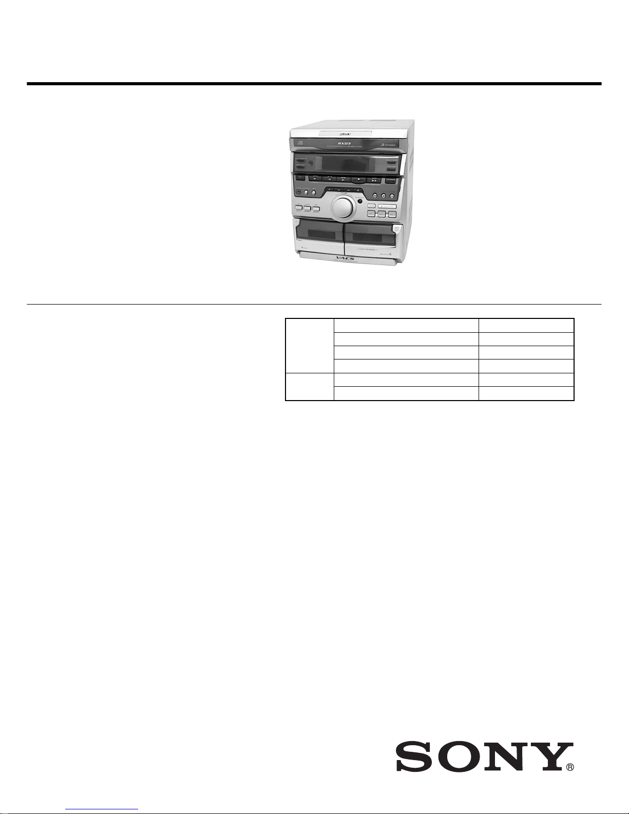
HCD-GRX20/RXD3
AEP Model
UK Model
HCD-RXD3
E Model
Australian Model
HCD-GRX20
SERVICE MANUAL
MINI Hi-Fi COMPONENT SYSTEM
— Continued on next page —
SPECIFICATIONS
Model Name Using Similar Mechanism NEW
CD Mechanism Type CX3
Base Unit Type KSM-213ECM
Optical Pick-up Type KSS-213ECM/C2NP
Model Name Using Similar Mechanism NEW
Tape T ransport Mechanism T ype CWL-44-FR
CD
SECTION
TAPE
DECK
SECTION
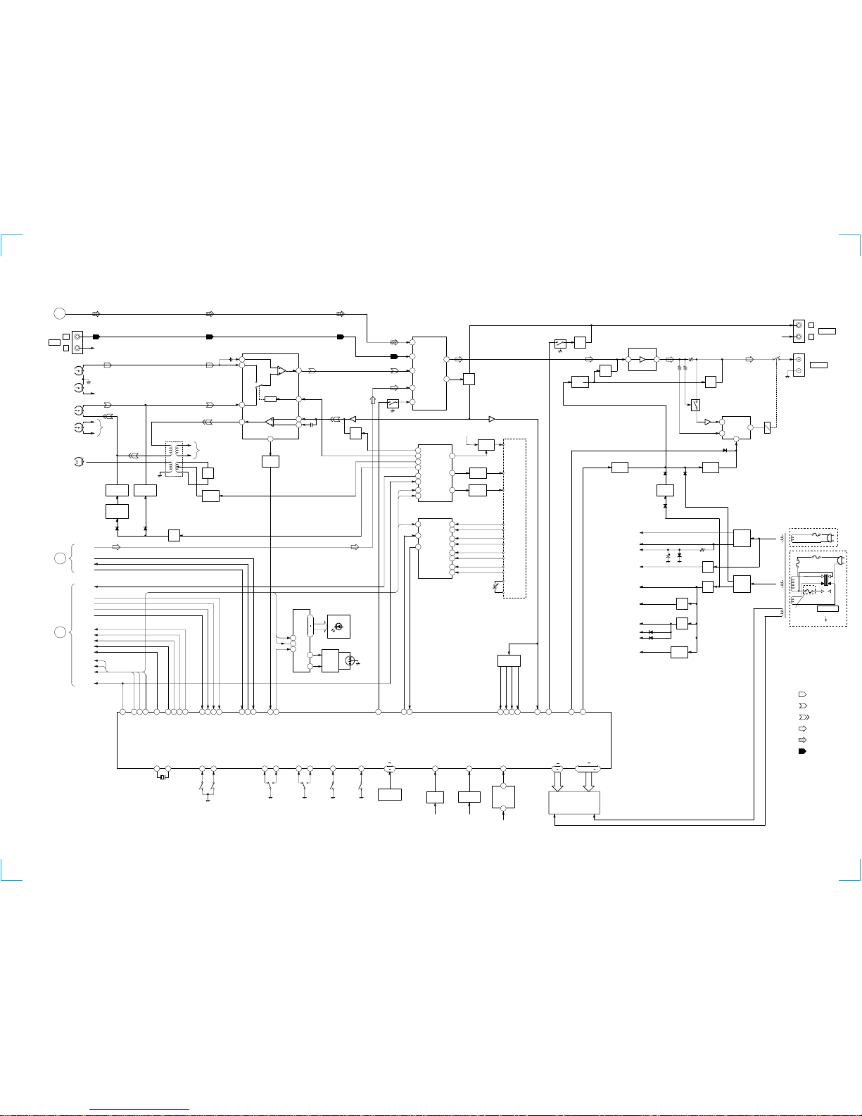
HCD-GRX20/RXD3 are the tuner, deck, CD
and amplifier section in MHC-GRX20/RXD3.
Sony Corporation
Home Audio Company
Published by Sony Engineering Corporation
9-928-949-13
2003E16-1
© 2003.05
PHOTO : HCD-RXD3
Amplifier section
European model
DIN power output (Rated) 40 W + 40 W
(6 Ω at 1 kHz, DIN)
Continuous RMS power output (Reference)
50 W + 50 W
(6 Ω at 1 kHz, 10%
THD)
Music power output (Reference)
100 W + 100 W
(6 Ω at 1 kHz, 10%
THD)
Other models
The following measured at AC 110, 220 V 60 Hz;
DIN power output (Rated) 45 W + 45 W
(6 Ω at 1 kHz, DIN)
Continuous RMS power output (Reference)
50 W + 50 W
(6 Ω at 1 kHz, 10%
THD)
The following measured at AC 120, 240 V 60 Hz;
DIN power output (Rated) 50 W + 50 W
(6 Ω at 1 kHz, DIN)
Continuous RMS power output (Reference)
60 W + 60 W
(6 Ω at 1 kHz, 10%
THD)
Inputs
MD IN (phono jack): voltage 450 mV,
impedance 47 kΩ
Outputs
MD OUT (phono jacks):
voltage 250 mV
impedance 1 kΩ
PHONES (stereo phone jack):
accepts headphones of 8
Ω or more.
SPEAKER: accepts impedance of 6
to 16 Ω
CD player section
System Compact disc and digital
audio system
Laser Semiconductor laser
(λ = 780 nm)
Emission duration:
continuous
Laser output Max. 44.6µW*
*This output is the value
measured at a distance of
200 mm from the
objective lens surface on
the Optical Pick-up
Block with 7 mm
aperture.
Frequency response 20Hz – 20kHz (±0.5 dB)
Wavelength 780 – 790 nm
DIGITAL OUT (OPTICAL)
(Square optical connector jack, rear panel)
Wavelength 600 nm
Output Level –18 dBm
Tape deck section
Recording system 4-track 2-channel stereo
Frequency response 40 – 13,000 Hz (±3 dB),
using Sony TYPE I
cassette
Wow and flutter ±0.15% W. Peak(IEC)
0.1% W. RMS(NAB)
±0.2% W. Peak(DIN)
Tuner section
FM stereo, FM/AM superheterodyne tuner
FM tunr section
Tuning range 87.5 – 108.0 MHz
Antenna FM lead antenna
Antenna terminals 75 Ω unbalanced
Intermediate frequency 10.7 MHz
Ver 1.2 2003. 05
2
SAFETY-RELATED COMPONENT WARNING!!
COMPONENTS IDENTIFIED BY MARK ! OR DOTTED LINE WITH
MARK ! ON THE SCHEMATIC DIAGRAMS AND IN THE PARTS
LIST ARE CRITICAL TO SAFE OPERATION. REPLACE THESE
COMPONENTS WITH SONY PARTS WHOSE PART NUMBERS
APPEAR AS SHOWN IN THIS MANUAL OR IN SUPPLEMENTS
PUBLISHED BY SONY .
Laser component in this product is capable
of emitting radiation exceeding the limit for
Class 1.
CAUTION
Use of controls or adjustments or performance of procedures
other than those specified herein may result in hazardous radiation
exposure.
Notes on chip component replacement
• Never reuse a disconnected chip component.
• Notice that the minus side of a tantalum capacitor may be
damaged by heat.
Flexible Circuit Board Repairing
• Keep the temperature of soldering iron around 270˚C
during repairing.
• Do not touch the soldering iron on the same conductor of the
circuit board (within 3 times).
• Be careful not to apply force on the conductor when soldering
or unsoldering.
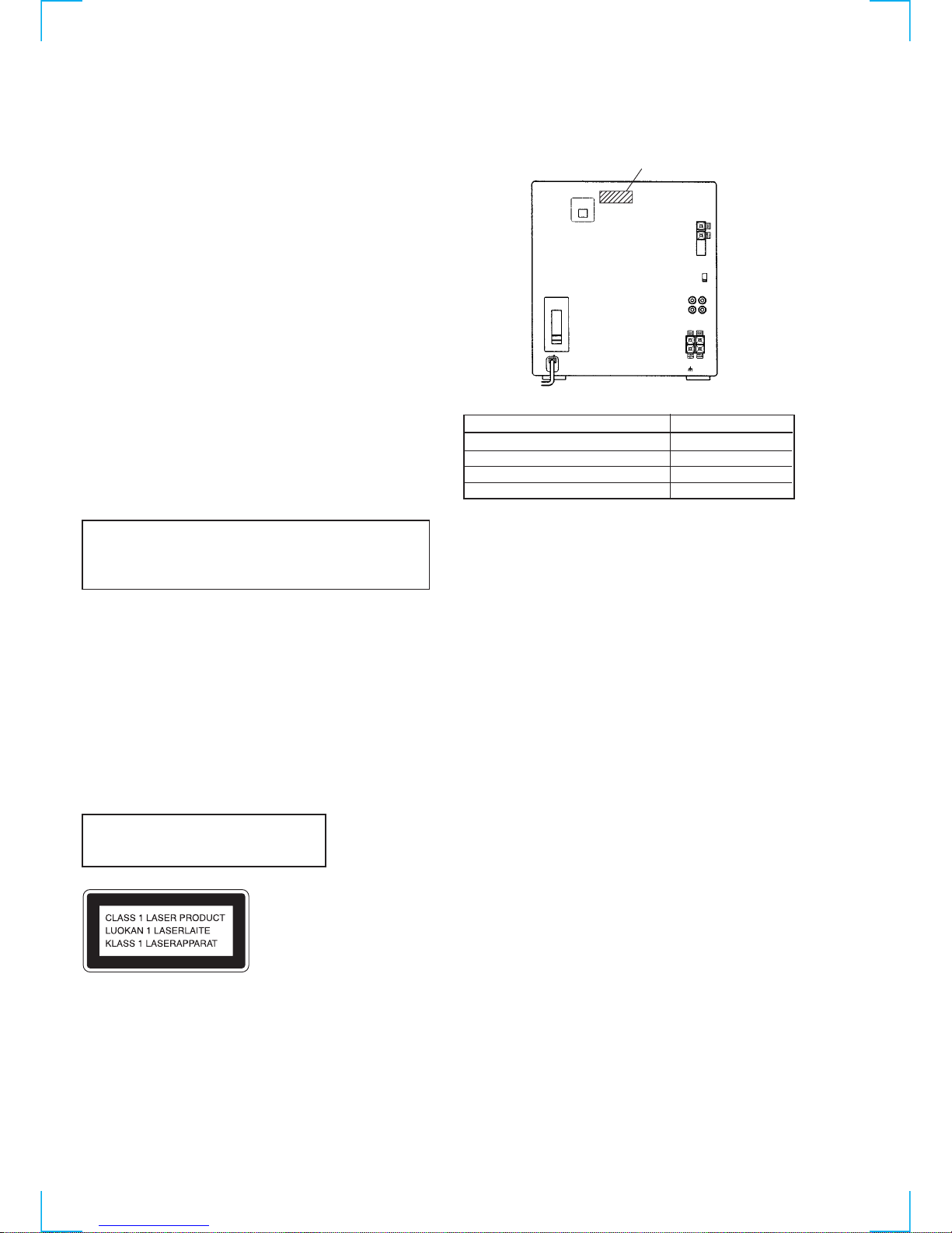
MODEL IDENTIFICATION
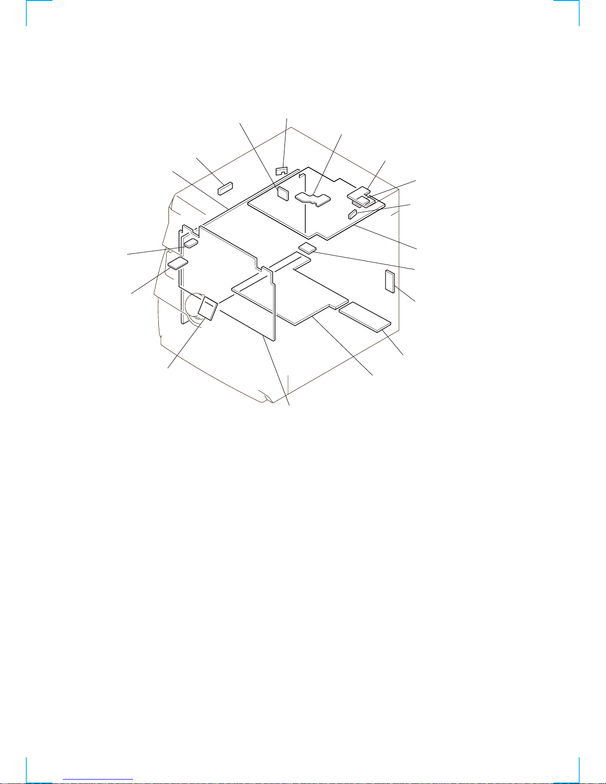
— CABINET, REAR —
• Abbreviation
AUS : Australian model
SP : Singapore model
MX : Mexican model
AR : Argentina model
TW : Taiwan model
PART NO.
RXD3 model 4-221-603-0π
GRX20 : AUS model 4-221-604-0π
GRX20 : AR, E, SP, TW models 4-221-605-0π
GRX20 : MX model 4-221-606-0π
PARTS No.MODEL
AM tuner section
Tuning renge 531 – 1,602 kHz
(with AM tuning interval set at 9 kHz)
530 – 1,710 kHz
(with AM tuning interval set at 10 kHz)
Antenna AM loop antenna
Antenna terminals External antenna terminal
Intermediate frequency 450 kHz
General
Power requirements
European model 230 V AC, 50/60 Hz
Mexican model 120 V AC, 50/60 Hz
Australian model 240 V AC, 50/60 Hz
Other models 110 – 120 V or 220 – 240 V AC, 50/60 Hz
(adjustable with voltage selector)
Power consumption
European model 105 W
Other models 115 W
Dimensions (w/h/d) incl. projecting parts and controls
Approx. 280 × 320 × 400 mm
(111/8 × 125/8 × 153/4 in)
Mass Approx. 9.2kg (20 lb 5 oz.)
Supplied accessories: AM loop antenna (1)
FM lead antenna (1)
Remote (1)
Plug adaptor (for Asian model) (1)
Design and specifications are subject to change without notice.

3
TABLE OF CONTENTS
1. GENERAL ·········································································· 4
2. DISASSEMBLY
2-1. CD Door ·············································································5
2-2. Front Panel ········································································· 6
2-3. Main Board········································································· 6
2-4. Amplifier Board ································································· 7
2-5. CD Tray ·············································································· 7
2-6. Decord Board ····································································· 8
2-7. Base Unit ············································································ 9
2-8. Cassette Lid ········································································ 9
3. TEST MODE ···································································· 10
4. MECHANICAL ADJUSTMENTS ····························· 11
5. ELECTRICAL ADJUSTMENTS ······························· 11
6. DIAGRAMS
6-1. Circuit Boards Location ··················································· 16
6-2. Block Diagrams ································································ 17
Main Section····································································· 17
Tuner, CD Section ···························································· 18
6-3. Printed Wiring Board Main Section ······························· 20
6-4. Schematic Diagram Main (1/3) Section ························· 21
6-5. Schematic Diagram Main (2/3) Section ························· 22
6-6. Schematic Diagram Main (3/3) Section ························· 23
6-7. Printed Wiring Board Front Panel Section ····················· 24
6-8. Schematic Diagram Front Panel Section ························ 25
6-9. Printed Wiring Board Amplifier Section ························ 26
6-10. Schematic Diagram Amplifier Section··························· 27
6-11. Printed Wiring Board CD Section ·································· 28
6-12. Schematic Diagram CD Section····································· 29
6-13. IC Pin Function ································································ 30
6-14. IC Block Diagrams··························································· 31
7. EXPLODED VIEWS
7-1. Cabinet Section································································· 35
7-2. Front Panel Section ·························································· 36
7-3. CD Mechanism Deck Section-1 ······································· 37
7-4. CD Mechanism Deck Section-2 ······································· 38
7-5. Base Unit Section (KSM-213ECM) ································· 39
8. ELECTRICAL PARTS LIST ······································· 40
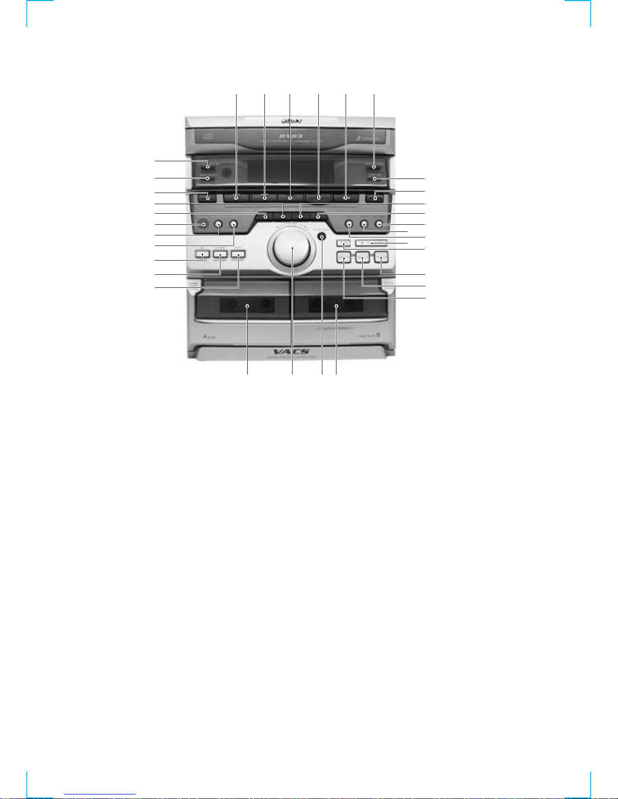
4
1 1/u (Power) button
2 TIMER SELECT button
3 CLOCK/TIMER SET button
4 ( (TAPE A) button
5 9 (TAPE B) button
6 ( (TAPE B) button
7 p (STOP) button
8 ^ (CD) button
9 DISPLAY/DEMO button
!º FUNCTION button
!¡ TUNER/BAND button
!™ + button
!£ + + button
!¢ CD SYNC button
!∞ PAUSE button
!§ REC button
!¶ 6 OPEN/CLOSE button
!• DISC SKIP/EX-CHANGE button
!ª DISC 3 button
@º DISC 2 button
@¡ DISC 1 button
@™ DECK B
@£ ENTER/NEXT button
@¢ VOLUME knob
@∞ DECK A
@§ REPEAT/STEREO/MONO button
@¶ PLAY MODE/TUNER MEMORY button
@• EDIT/DIRECTION button
@ª DBFB button
#º FILE SELECT button
#¡ PHONES jack
#™ = – button
#£ = button
SECTION 1
GENERAL
4
3
2
#¡
@¶
@•
@§
@∞
@¢
@£
@™
@¡
@º
!ª
!§
!∞
!¶
!•
!¢
!£
!™
56 78 9
!º
!¡
1
#£
#™
#º
@ª
5
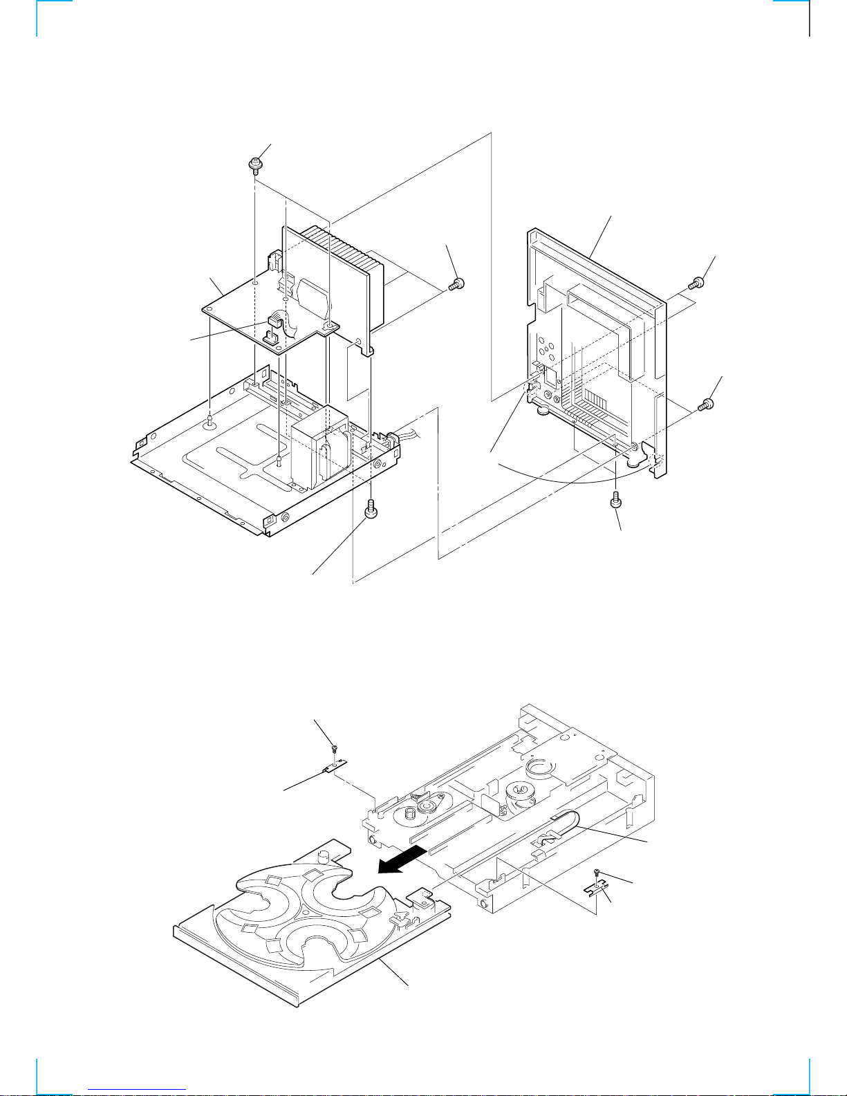
SECTION 2
DISASSEMBLY
Note : Follow the disassembly procedure in the numerical order given.
2-1. CD DOOR
8
CD door
5
Top cover
4
Remove the
claws
4
Remove the
claws
7
Remove the
claws
2
Three screws
1
Three srews
3
Five screws
6
Pull out the CD tray and remove the
CD door with releasing claws into the
directioin of arrow.

6
2-2. FRONT PANEL
2-3. MAIN BOARD
9
Board to board
connectors
(CN602)
(CN601)
MAIN board
3
Harness
(CN303)
1
Three screws
2
Screw
!º
Front panel
4
Flat type wir
e
(CN705)
5
Flat type wire
(CN501)
7
Connector
(CN201)
8
Remove the
claws
6
Connector
(to deckB)
6
Five screws
4
CD mechanism deck
2
T wo screws
3
Connector
(CN703)
5
Harness (CN701)
1
Harness (CN301)
7
MAIN board
7
2-4. AMPLIFIER BOARD
2-5. CD TRA Y
2
T wo screws
6
Rear cover
5
Remove the claws
4
T wo screws
1
Connector
(CN703)
8
Three screws
7
Three screws
9
Three screws
!º
AMPLIFIER board
3
Three screw
s
1
Screw
2
Bracket
4
Bracket
5
Flat type wir
e
(CN06)
3
Screw
6
CD tray
8
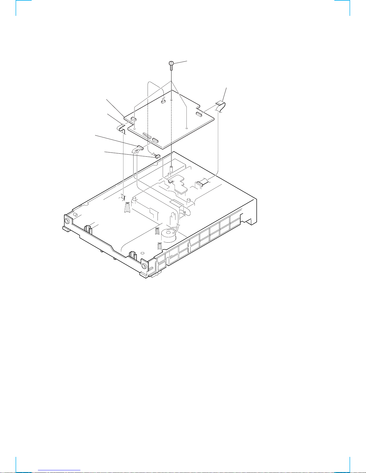
2-6. DECORD BOARD
4
Three screws
6
CD decode board
1
Flat cable
(CN706)
3
Flat cable (CN701
)
2
Connector
(CN707)
5
Connector
(CN702)
9
2-8. CASSETTE LID
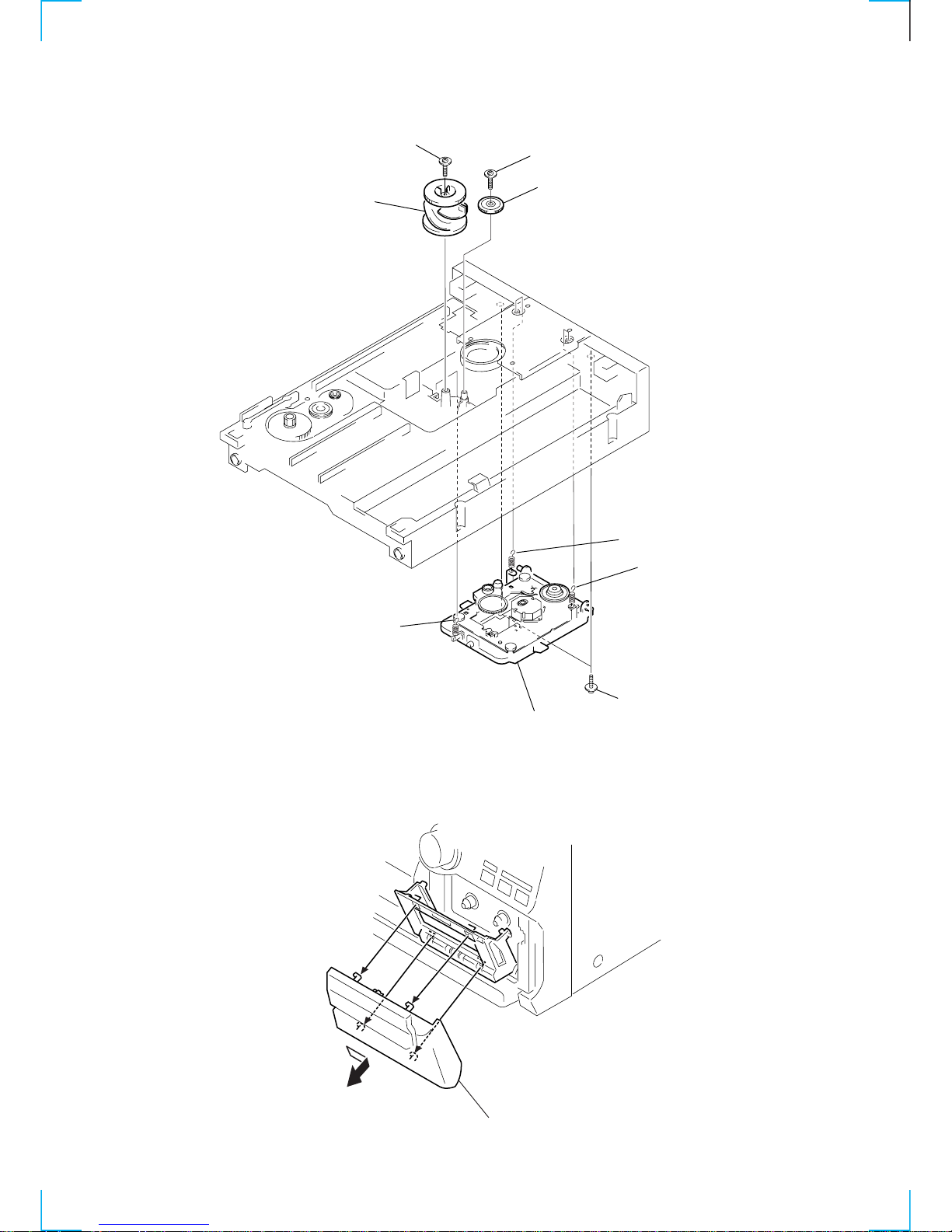
2-7. BASE UNIT
2
Screw
3
UD-gear
4
Screw
5
UD-Cam
8
Spring
7
Spring
6
Spring
1
T wo screws
9
Base unit
Cassette door
(Note: Four claws are used.)

10
SECTION 3
TEST MODE
Function Key combination Description
Initialization
STOP + POWER OFF All preset data is re-set to the initial
(default) value.
Model display
STOP + DISC 1 Mode name is displayed.
Destination display
STOP + DISC 2 Destination is displayed.
Version display
STOP + DISC 3 Version number of the
microprocessor is displayed.
CD aging mode
STOP + DISC SKIP/EX-CHANGE Set discs to DISC 1 and DISC
3. The following operations are repeated when aging
starts:
1. DISC 1: TOC Read
2. Plays back the last music of the DISC 1.
3. DISC 3 : TOC Read
4. Plays back the last music of the DISC 3.
5. STOP
6. Tray is open and closed.
TAPE aging mode
STOP + PLAY A Insert a commercially available cassette tape (10
min) to the decks A and B. When aging starts, each tape is rewound
and the following
operations are repeated:
1. TAPE A: FWD PLAY for one minute
2. TAPE A: FWD STOP for one second
3. TAPE A: FWD PLAY for three minutes
4. TAPE A: FWD FF to tape end
5. TAPE B: FWD PLAY for one minute
6. TAPE B: FWD REC PAUSE for one second
7. TAPE B: FWD REC for three minutes
8. TAPE B: FWD FF to tape end
9. TAPE B: REV PLAY for one minute
10. TAPE B: REV REC PAUSE for one second
11. TAPE B: REV REC for three minutes
12. TAPE B: REV FF to tape end.
CD service mode
STOP + OPEN/CLOSE The message “CD S - -” is displayed on the
screen. The sled is moved to the outer circumference
while the FF button is pressed. Also, the SLED is moved to the
inner
circumference while the REW button is pressed. After pressing the
PLA Y
button, FOCUS is turned ON, CL V-S is set, TRACKING and SLED
servos
are turned OFF and ADDRESS 3 = 3F, 37 is set.
Display
STOP + DBFB All displays are turned ON.
Balance adjustment value
STOP + DISPLAY/DEMO The balance adjustment value is
displayed.
Key check
STOP + FILE SELECT Function of the pressed key is displayed.
11
Precaution
1. Clean the following parts with a denatured alcohol-moistened
swab:
record/playback head pinch rollers
erase head rubber belts
capstan idlers
2. Demagnetize the record/playback head with a head
demagnetizer.
3. Do not use a magnetized screwdriver for the adjustments.
4. After the adjustments, apply suitable locking compound to the
parts adjusted.
5. The adjustments should be performed with the rated power
supply voltage unless otherwise noted.
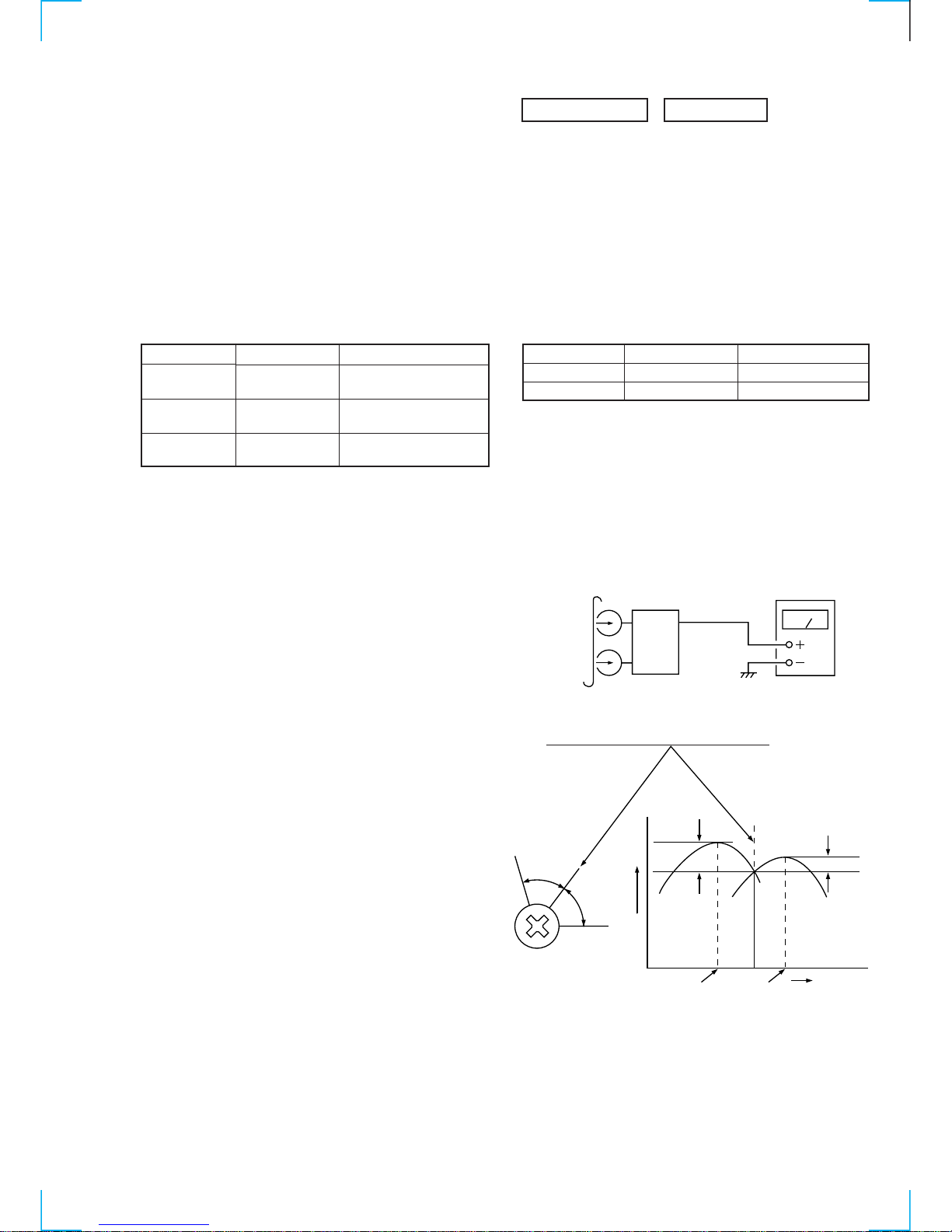
Torque Measurement
SECTION 4
MECHANICAL ADJUSTMENTS
Meter reading
40 to 70 g • cm
(0.56 - 0.97 oz • inch)
1 to 5 g • cm
(0.01 - 0.07 oz • inch)
55 to 140 g • cm
(0.76 - 1.94 oz • inch)
Torque
FWD
FWD
back tension
FF/REW
Torque meter
CQ-102C
CQ-102C
CQ-201B
SECTION 5
ELECTRICAL ADJUSTMENTS
1. Demagnetize the record/playback head with a head
demagnetizer.
2. Do not use a magnetized screwdriver for the adjustments.
3. After the adjustments, apply suitable locking compound to the
parts adjusted.
4. The adjustments should be performed with the rated power
supply voltage unless otherwise noted.
5. The adjustments should be performed in the order given in this
service manual. (As a general rule, playback circuit adjustment
should be completed before performing recording circuit
adjustment.)
6. The adjustments should be performed for both L-CH and RCH.
Record/Playback Head Azimuth Adjustment
(Deck A, Deck B)
Note: Perform this adjustments for both decks.
Procedure:
1. Mode : Playback
2. Turn the adjustment screw and check output peaks. If the peaks
do not match for L-CH and R-CH, turn the adjustment screw
so that outputs match within 2 dB of peak.
DECK SECTION 0 dB=0.775V
Tape
P-4-A100
WS-48B
Signal
10 kHz, –10 dB
3 kHz, 0 dB
Used for
Azimuth Adjustment
Tape Speed Adjustment
test tape
P-4-A100
(10kHz, –10dB)
set
SPEAKER
terminal (JK401)
level meter
L-CH
peak
R-CH
peak
screw
position
output
level
within
2dB
L-CH
peak
R-CH
peak
screw
position
within 2dB
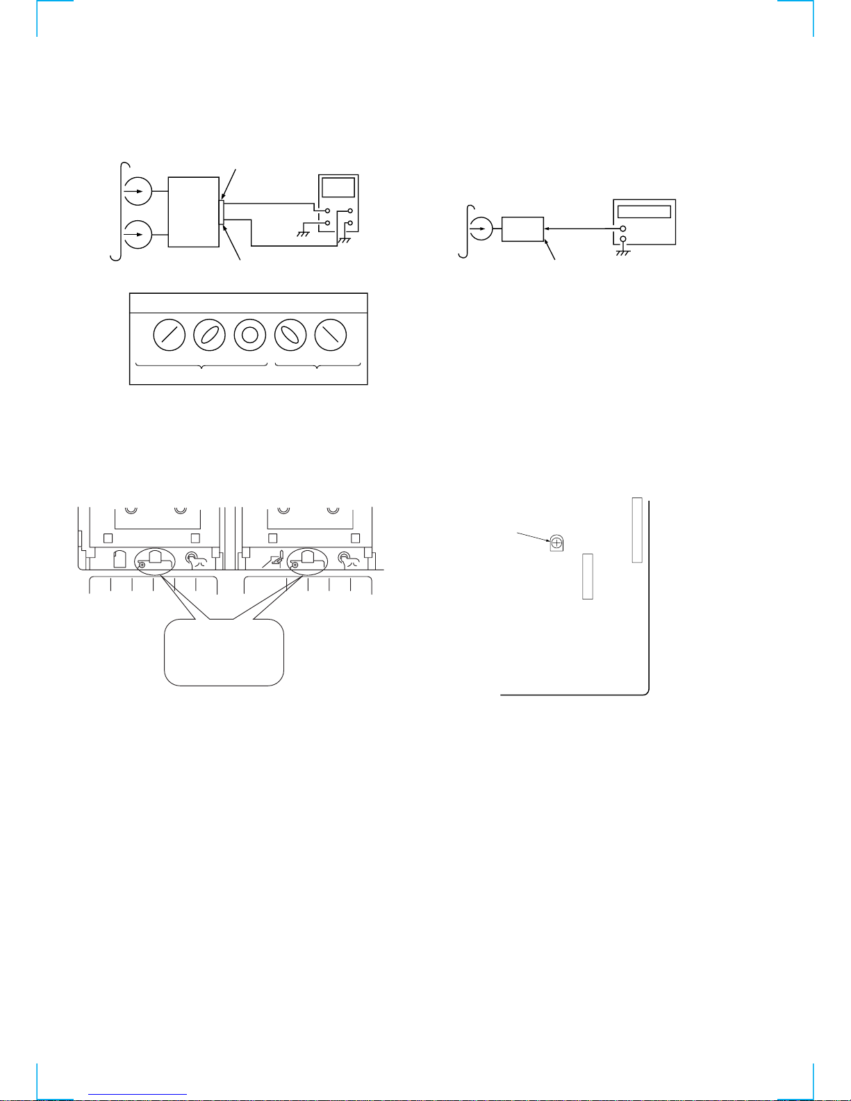
12
3. Mode: Playback
4. After the adjustments, apply suitable locking compound to the
parts adjusted.
Adjustment Location:
Remove the cassette lid before adjustment (See page 9)
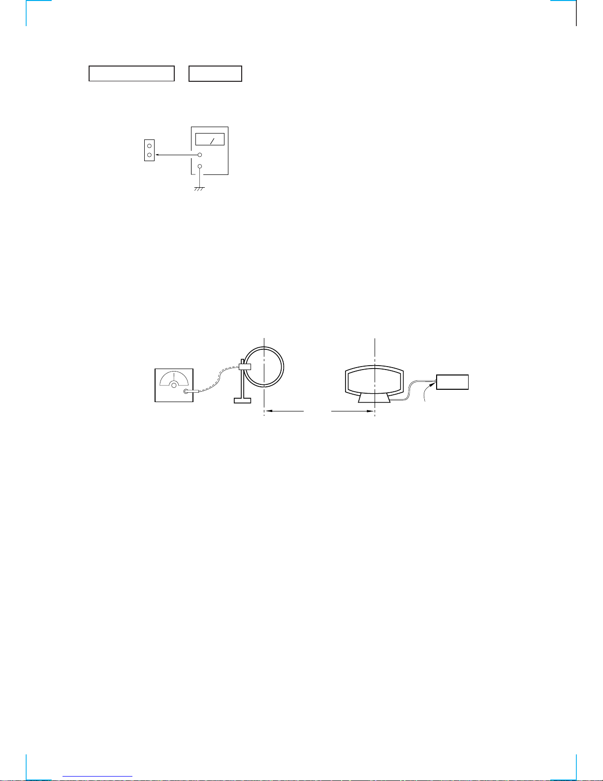
Tape Speed Adjustment (Deck A)
Procedure:
1. Mode: Playback
2. Adjust the SFR501 so that the frequency counter reads 3,000
Hz ± 90Hz.
Adjustment Location: MAIN board
Sample Value of Wow and flutter
W. RMS (JIS) within 0.3%
(test tape: WS-48B)
[MAIN BOARD] — Component side —
test tape
P-4-A100
(10kHz, –10dB)
SPEAKER
terminal (JK401)
(L-CH)
SPEAKER
terminal (JK401)
(R-CH)
oscilloscop
e
L
R
Waveform of oscilloscope
in phase 45˚ 90˚ 135˚ 180˚
good wrong
Adjustment screws
REC/PB head (deck B)
or PB head (deck A)
test tape
WS-48B
(3kHz, 0dB)
set
SPEAKER
terminal (JK401)
frequency counte
r
+
–
Tape Speed
CN501
CN601
SFR501
13
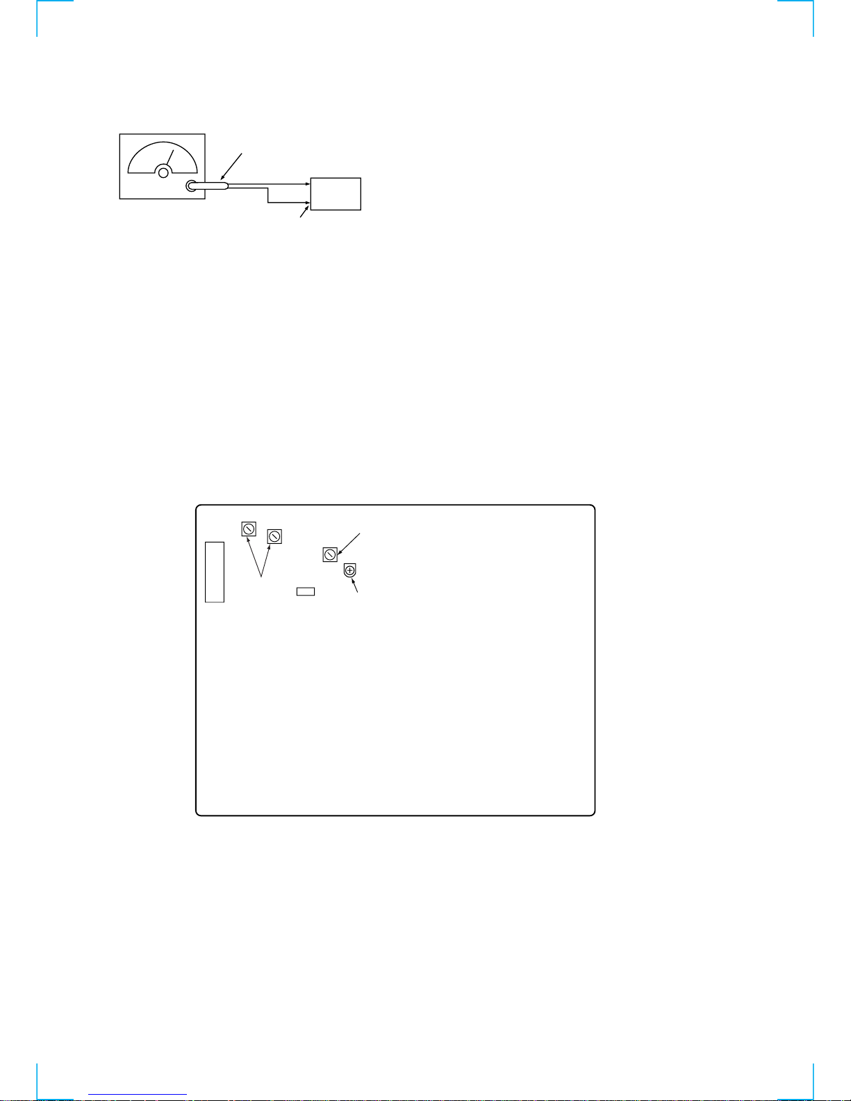
TUNER SECTION 0 dB=1µV
AM T uning Voltage Adjustment
Procedure:
1. Set the reception frequency of the unit to 530 kHz.
2. Adjust L105 for 1.2 ± 0.05 V reading on the DC voltmeter.
3. Set the reception frequency of the unit to 1,710 kHz.
4. Confirm that the voltage reading on the DC voltmeter is within
8.0 ± 0.5 V.
Adjustment Location: MAIN board (See page 14)
AM Trac king Adjustment
Procedure:
1. Tune the set to 600 kHz.
2. Set the output of AM RF SSG so that the input lev el of the set
will become 60 dB (µV/m).
3. Adjust L104 so that when the waveform on the oscilloscope is
maximum, no noise appears.
4. Tune the set to 1,400 kHz.
5. Adjust TC102 so that when the waveform on the oscilloscope
is maximum, no noise appears.
• Repeat the procedures in each adjustment several times, and the
tracking adjustment should be finally done by the trimmer
capacitors.
Adjustment Location: MAIN board (See page 14)
Main board
TP1
G
VT
DC voltmete
r
+
–
AM RF SSG
loop antenna
set
loop antenna
(Supplied accessories)
60 cm
AM ANTENNA
terminal (TM1)
30% amplitude
modulation by
400 Hz signal
Field strength dB (
µ
V/m) =SSG output level dB (µV/m) –26 dB.
14
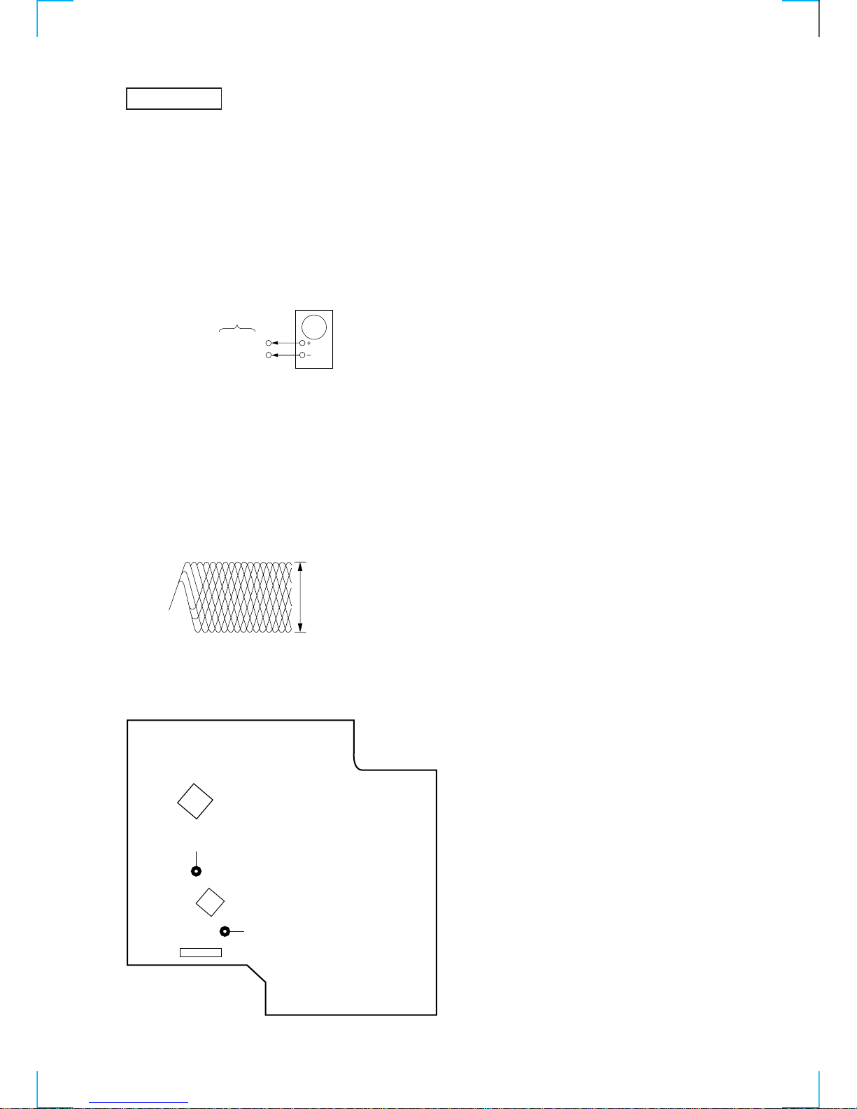
FM Tuned Level Adjustment
Procedure:
1. Supply a 28 dB 98 MHz signal from the ANTENN A terminal.
2. Tune the set to 98 MHz.
3. Adjust SFR101 to the point (moment) when the TUNED
indicator will change from going off to going on.
Adjustment Location: MAIN board
Adjustment Location
[MAIN BOARD] — Component side —
FM RF SSG
75
Ω
coaxial
Carrier frequency : 98 MHz
Modulation : AUDIO 1 kHz, 75 kHz
deviation (100%)
Output level : 28 dB (at 75 W open)
FM ANTENNA terminal
(JK101)
set
L104
TC102
TP1
SFR101
L105
FM T uned Level
AM T uning
Voltage
AM T rac king
JK101
15
CD SECTION
Note:
1. CD Block is basically constructed to operate without
adjustment. Therefore, check each item in order given.
2. Use YEDS-18 disc (3-702-101-01) unless otherwise indicated.
3. Use an oscilloscope with more than 10MΩ impedance.
4. Clean the object lens by an applicator with neutral detergent
when the signal level is low than specified value with the
following checks.
5. Adjust the focus bias adjustment when optical block is replaced.
RF Level Check
Procedure :
1. Connect oscilloscope to test point TP (RF) on CD DECODER
board.
2. Turned Power switch on.
3. Put disc (YEDS-18) in and playback.
4. Confirm that oscilloscope waveform is clear and check RF
signal level is correct or not.
Note: Clear RF signal waveform means that the shape “◊” can be
clearly distinguished at the center of the waveform.
Adjustment Location:
[CD DECODER BOARD] — Component side —
CD DECODER
board
oscilloscope
TP (RF)
TP (VC)
VOLT/DIV: 200 m
V
TIME/DIV: 500 nS
level: 1.0 Vp-p
+0.3
–0.2
IC702
IC701
J778
J789
TP (VC)
TP
(RF)
CN701
16
SECTION 6
DIAGRAMS
6-1. CIRCUIT BOARDS LOCATION
MAIN board
CD DECORD board
TR board
AC SWITCH board
FRONT board
SW (A) board
PHOTO SOCKET board
SW (B) board
SW (C) board
SW (D) board
MOTOR board
H/P board
VR board
SENSOR board
MOTOR (6P) (S) board
FUSE board
AMPLIFIER board
HCD-GRX20/RXD3
1717
HP901
PB
HEAD
TAPE B
HRP901
REC/PB
HEAD
TAPE A
R CHR CH
R CH
PLAY/REC
CONTROL
Q203, 205
PLAY/REC
CONTROL
DRIVE
Q207
PLAY/REC
CONTROL
D201
L291
BIAS OSC
BIAS
OSC
Q251
HE901
ERASE
HEAD
R CH
1
2
9
3
REC OUT
PB OUT
A/B
5
19
11
10
REC/PB
EQ AMP
IC201
TAPE A/B
Q213
MUTE
Q320
AMS
Q551,552
D202
: FM
: CD
• Signal Path
• RCH is omitted
C
CD
SECTION
TU L
ST IND
TU MUTE
DO1
Q401
MUTE
14 7
4
POWER AMP
IC401
SPEAKER
RELAY
DRIVE
Q403
Q405
1
2
6
IC402
RL401
SPEAKER
JK401
SCOR
SENS1
SQSO
XLAT
SQCK
CLK
DI
CLK
CE
STB
11
STB
21CE25
SCLK
27
SDATA OUT
24
DATA22SQCK
20
XLAT
23
SQSO
42
SENS1
4
SCOR
26
SDATA IN
MUTE
DRIVE
Q411
MUTE
SWITCH
Q603,604
62
TU MUTE
28
FM ST IND
17
CTRL
63
SYSTEM MUTE
64
POWER SW
LED DRIVE
IC602
2
3
4
19
ALATCH
11
LED
DRIVE
DI
CLK
Q607,608
LED602-607
LED601
XTAL40XTAL
39
VR UP
52
X601
10MHz
VR DOWN
53
VR601
VOLUME
PIC UP
46
PIC DOWN
47
TRAY OPEN
50
TRAY CLOSE
51
TURN TABLE
49
DISC COUNT
48
A
B
S02
TRAY
OPEN/CLOSE
DET
S03
DISC
COUNTER
DET
S04
TURNTABLE
OPERATION
DET
S01
CD DECK
UP/DOWN
DET
KEY
MATRIX
S601-629
P2 P24
KI0 KI2
FLD601
FLD DISPLAY
SYSTEM CONTROLLER/
FLD DRIVER
IC601
+5.6V
REG
Q308
SITCHING
Q705
+5V
+12V
+7.5V
REG
Q702
CD +7.5V
+12V
REG
Q701
RECT
D705-708
P MUTE
CONT
Q703
AC OFF
DET
Q704
D713
D704
RECT
D701
-12V
IC401 B-
IC401 B+
-27V
REG
Q705
-27V
T001
AC4.8V
AC4.8V
16
A
TUNER
SECTION
: PB (DECK A)
: PB (DECK B)
: REC (DECK B)
Q207
Q201
CE
CLK
DI
12
LOCK
MUTE
Q208,209
BIAS
SWITCH
Q252,253
6
Q351
TAPE (L)
4
TUNER (L)
3
CD (L)
2
B
CD
SECTION
CD L
LINE AMP
IC301
9VOL OUT
BUS REGISTER
IC501
REC MUTE
13
A/B
11
BIAS
12
PLAY MUTE
14
DI
2
CLK
3
STB
1
DI
CLK
CONT
11
4PLAY
5SOL A
6
SOL B
SOL A
DRIVE
Q505,506
M+12V
SWITCH
Q501,502
M+12V
SOL B
DRIVE
Q503,504
SHIFT REGISTER
IC502
CK
2
S/L
1
QH
9
CLK
3
B REC FWD
5
PHOTO A
11
A MODE SW
13
A HALF
6
PHOTO B
12B MODE SW
14
B HALF
MECHA
BLOCK
SFR501
MOTOR H/L
Q412
MUTE
D406
+5.6V
66 8829 31
G1 G13
Q'S
10
DATA IN
DATA
SENS2
LOCK
13
CLOK
43
SENS2
37
AMS
12
10
S/L
9
DATA IN
L
R
MD
JK301
R CH
MD (L)
5
: MD
1
REC OUT AMP
Q306
Q302
4
B REC REV
Q320
Q551
MUTE
L
R
LINE OUT
JK301
R CH
D405
µCON B+
VCC
D602
D601
RESET
SWITCH
POWER
DOWN DET
Q601
Q602
2
3
RM601
REMOTE
CONTROL
RECEIVER
RESET
38
POWER DOWN
6
REMOTE
8
VCC
VCCVCC
21.100 90
.
61
MD MUTE
32
VACS
36
SPEANA 4
SPEANA
35
SPEANA 334SPEANA 233SPEANA 1
13
10
8
5
.
.
(Page 18)
(Page 18)
(Page 18)
AC IN
F702
F703
SW401
AC IN
F702
GRX20 : AUS, RXD3 MODEL
AC VOLTAGE
GRX20:
E,SP,TW
MODELS
GRX20 : E,SP,TW,MX,AR MODELS
220 – 240 V
110 – 120 V
• Abbreviation
AUS : Australian model
SP : Singapore model
MX : Mexican model
AR : Argentina model
TW : Taiwan model
6-2. BLOCK DIAGRAMS
MAIN SECTION
 Loading...