

Sony HCD-GPX555, HCD-GPX888 Schematic

HCD-GPX555/GPX888
SERVICE MANUAL
Ver. 1.1 2014.10
• HCD-GPX555 is the amplifi er, USB, CD player,
Bluetooth, NFC and tuner section in MHC-GPX555.
• HCD-GPX888 is the amplifi er, USB, CD player,
Bluetooth, NFC and tuner section in MHC-GPX888. Photo: HCD-GPX888
• “WALKMAN” and “WALKMAN” logo are registered trademarks of Sony Corporation.
• MPEG Layer-3 audio coding technology and patents licensed from Fraunhofer IIS and Thomson.
• Windows Media is either a registered trademark or trademark of Microsoft Corporation in the United States and/or
other countries.
• This product is protected by certain intellectual property rights of Microsoft Corporation. Use or distribution of
such technology outside of this product is prohibited without a license from Microsoft or an authorized Microsoft
subsidiary.
• The Bluetooth
• The N Mark is a trademark or registered trademark of NFC Forum, Inc. in the United States and in other countries.
• Android™ is a trademark of Google Inc.
• Google Play™ is a trademark of Google Inc.
• iPhone and iPod touch are trademarks of Apple Inc., registered in the U.S. and other countries. App Store is a service
• “Made for iPod” and “Made for iPhone” mean that an electronic accessory has been designed to connect specifically
• All other trademarks and registered trademarks are of their respective holders. In this manual, ™ and ® marks are not
®
marks by Sony Corporation is under license. Other trademarks and trade names are those of their respective owners.
mark of Apple Inc.
to iPod or iPhone, respectively, and has been certified by the developer to meet Apple performance standards. Apple is
not responsible for the operation of this device or its compliance with safety and regulatory standards. Please note that
the use of this accessory with iPod or iPhone may affect wireless performance.
specified.
word mark and logos are registered trademarks owned by Bluetooth SIG, Inc. and any use of such
CD Section
US Model
HCD-GPX555
E Model
HCD-GPX555/GPX888
Australian Model
HCD-GPX555
Model Name Using
Similar Mechanism
CD Mechanism Type CDM90-DVBU204//M
Optical Pick-up Name CMS-S76RFS7G
HCD-GPX33
AUDIO POWER SPECIFICATIONS
POWER OUTPUT AND TOTAL HARMONIC
DISTORTION:
(USA model only)
With 4 ohm loads, both channels driven, from
120 – 10,000 Hz; rated 180 watts per channel
minimum RMS power, with no more than
0.7% total harmonic distortion from 250
milliwatts to rated output.
Amplifi er section
The following are measured at
USA model:
AC 120 V, 60 Hz
Mexican model:
AC 120 V – 240 V, 60 Hz
Chilean and Bolivian models:
AC 220 V – 240 V, 50 Hz
Other models:
AC 120 V – 240 V, 50/60 Hz
MHC-GPX888
Front speaker
Power Output (rated):
350 W + 350 W (at 4 ohms, 1 kHz,
1% THD)
RMS output power (reference):
600 W + 600 W (per channel at
4 ohms,
LBT-GPX555/MHC-GPX555
Front speaker
Power Output (rated):
350 W + 350 W (at 4 ohms, 1 kHz,
1% THD)
RMS output power (reference):
600 W + 600 W (per channel at 4 ohms,
1 kHz)
Subwoofer
RMS output power (reference):
600 W (4 ohms, 100 Hz)
1 kHz)
SPECIFICATIONS
Inputs
AUDIO IN 1/PARTY CHAIN IN L/R
Voltage 2 V, impedance 47 kilohms
AUDIO IN 2 L/R
Voltage 2 V, impedance 47 kilohms
MIC (MHC-GPX888 only)
Sensitivity 1 mV, impedance
10 kilohms
(USB) A, (USB) B, port
Type A
Outputs
AUDIO OUT/PARTY CHAIN OUT L/R
Voltage 2 V, impedance 1 kilohm
USB section
Supported bit rate
WMA:
48 kbps – 192 kbps, VBR, CBR
AAC:
48 kbps – 320 kbps, VBR, CBR
Sampling frequencies
WMA: 44.1 kHz
AAC: 44.1 kHz
Supported USB device
Mass Storage Class
Maximum current
500 mA
Disc/USB section
Supported bit rate
MPEG1 Layer-3:
32 kbps – 320 kbps, VBR
MPEG2 Layer-3:
8 kbps – 160 kbps, VBR
MPEG1 Layer-2:
32 kbps – 384 kbps, VBR
Sampling frequencies
MPEG1 Layer-3:
32 kHz/44.1 kHz/48 kHz
MPEG2 Layer-3:
16 kHz/22.05 kHz/24 kHz
MPEG1 Layer-2:
32 kHz/44.1 kHz/48 kHz
Disc player section
System
Compact disc and digital audio system
Laser Diode Properties
Emission Duration: Continuous
Laser Output*: Less than 44.6 W
* This output is the value measurement
at a distance of 200 mm from the
objective lens surface on the Optical
Pick-up Block with 7 mm aperture.
Frequency response
20 Hz – 20 kHz
Signal-to-noise ratio
More than 90 dB
Dynamic range
More than 88 dB
Tuner section
FM stereo, FM/AM superheterodyne tuner
Antenna:
FM lead antenna
AM loop antenna
FM tuner section
Tuning range
USA model:
87.5 MHz – 108.0 MHz
(100 kHz step)
Other models:
87.5 MHz – 108.0 MHz (50 kHz step)
AM tuner section
Tuning range
Pan American and Australian models:
531 kHz – 1,710 kHz (9 kHz step)
530 kHz – 1,710 kHz (10 kHz step)
Other models:
531 kHz – 1,602 kHz (9 kHz step)
530 kHz – 1,610 kHz (10 kHz step)
COMPACT DISC RECEIVER
Bluetooth section
Communication system
Bluetooth Standard version 3.1
Output
Bluetooth Standard Power Class 2
Maximum communication range
Line of sight approx. 10 m
Frequency band
2.4 GHz band (2.4000 GHz – 2.4835 GHz)
Modulation method
FHSS (Freq Hopping Spread Spectrum)
Compatible Bluetooth profiles
A2DP (Advanced Audio Distribution
Profile)
AVRCP 1.3 (Audio Video Remote
Control Profile)
SPP (Serial Port Profile)
Supported codecs
SBC (Sub Band Codec)
AAC (Advanced Audio Coding)
1)
The actual range will vary depending on
factors such as obstacles between devices,
magnetic fields around a microwave oven,
static electricity, reception sensitivity,
antenna’s performance, operating system,
software application, etc.
2)
Bluetooth standard profiles indicate the
purpose of Bluetooth communication
between devices.
1)
2)
– Continued on next page –
9-890-651-02
2014J80-1
2014.10
©
Sony Corporation
Published by Sony EMCS (Malaysia) PG Tec
HCD-GPX555/GPX888
5
Ver. 1.1
General
Power requirements
USA model:
AC 120 V, 60 Hz
Mexican model:
AC 120 V – 240 V, 60 Hz
Chilean and Bolivian models:
AC 220 V – 240 V, 50 Hz
Other models:
AC 120 V – 240 V, 50/60 Hz
Power consumption
MHC-GPX888: 360 W
LBT-GPX555/MHC-GPX555: 280 W
Dimensions (w/h/d) (excl. speakers)
(Approx.)
MHC-GPX888:
294 mm × 361 mm × 331 mm
(11
⁄8 in × 14 1⁄4 in × 13 1⁄8 in)
LBT-GPX555/MHC-GPX555:
294 mm × 361 mm × 325 mm
(11 5⁄8 in × 14 1⁄4 in × 12 7⁄8 in)
Mass (excl. speakers) (Approx.)
5.4 kg (11 lb 15 oz)
Supplied accessories
Remote control (1)
R6 (Size AA) batteries (2)
FM lead/AM loop antenna (1)
Spacer (2) (MHC-GPX888 only)
Speaker pads (16) (MHC-GPX888 only)
Design and specifi cations are subject to change without notice.
NOTES ON CHIP COMPONENT REPLACEMENT
• Never reuse a disconnected chip component.
• Notice that the minus side of a tantalum capacitor may be
damaged by heat.
FLEXIBLE CIRCUIT BOARD REPAIRING
• Keep the temperature of soldering iron around 270 °C during
repairing.
• Do not touch the soldering iron on the same conductor of the
circuit board (within 3 times).
• Be careful not to apply force on the conductor when soldering
or unsoldering.
SAFETY CHECK-OUT
After correcting the original service problem, perform the
following safety check before releasing the set to the customer:
Check the antenna terminals, metal trim, “metallized” knobs,
screws, and all other exposed metal parts for AC leakage.
Check leakage as described below.
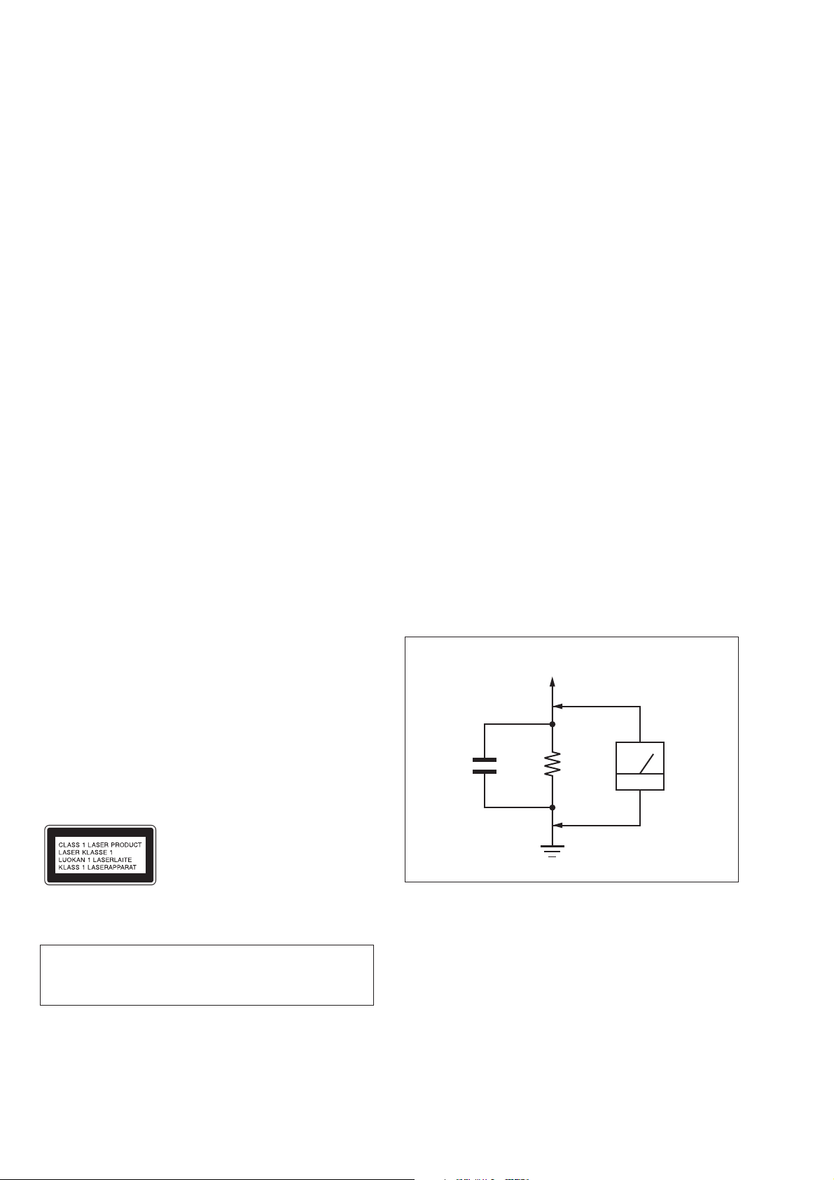
LEAKAGE TEST
The AC leakage from any exposed metal part to earth ground and
from all exposed metal parts to any exposed metal part having a
return to chassis, must not exceed 0.5 mA (500 microamperes.).
Leakage current can be measured by any one of three methods.
1. A commercial leakage tester, such as the Simpson 229 or RCA
WT-540A. Follow the manufacturers’ instructions to use these
instruments.
2. A battery-operated AC milliammeter. The Data Precision 245
digital multimeter is suitable for this job.
3. Measuring the voltage drop across a resistor by means of a
VOM or battery-operated AC voltmeter. The “limit” indication
is 0.75 V, so analog meters must have an accurate low-voltage
scale. The Simpson 250 and Sanwa SH-63Trd are examples
of a passive VOM that is suitable. Nearly all battery operated
digital multimeters that have a 2 V AC range are suitable. (See
Fig. A)
This appliance is classified as a CLASS 1
LASER product by IEC60825-1:2007. This
marking is located on the rear exterior.
CAUTION
Use of controls or adjustments or performance of procedures
other than those specifi ed herein may result in hazardous
radiation exposure.
SAFETY-RELATED COMPONENT WARNING!
COMPONENTS IDENTIFIED BY MARK 0 OR DOTTED LINE
WITH MARK 0 ON THE SCHEMATIC DIAGRAMS AND IN
THE PARTS LIST ARE CRITICAL TO SAFE OPERATION.
REPLACE THESE COMPONENTS WITH SONY PARTS
WHOSE PART NUMBERS APPEAR AS SHOWN IN THIS
MANUAL OR IN SUPPLEMENTS PUBLISHED BY SONY.
To Exposed Metal
Parts on Set
AC
1.5 kΩ0.15 μF
voltmeter
(0.75 V)
Earth Ground
Fig. A. Using an AC voltmeter to check AC leakage.
2

TABLE OF CONTENTS
HCD-GPX555/GPX888
1. SERVICING NOTES
................................................ 4
2. DISASSEMBLY
2-1. Disassembly Flow ........................................................... 7
2-2. Side-L Panel, Side-R Panel, Top Panel ........................... 8
2-3. Loading Panel ................................................................. 8
2-4. Front Panel Section ......................................................... 9
2-5. CD Mechanism Section (CDM90-DVBU204//M) ......... 9
2-6. Back Panel Section ......................................................... 10
2-7. MB Board, DAMP Board ............................................... 10
2-8. SWITCHING REGULATOR (3H401W) ....................... 11
2-9. Service Optical Device, Wire (Flat Type) ....................... 12
3. TEST MODE ............................................................. 13
4. ELECTRICAL CHECK .......................................... 16
5. TROUBLESHOOTING ........................................... 17
6. DIAGRAMS
6-1. Block Diagram - RS SERVO, USB Section - ................. 23
6-2. Block Diagram - MAIN Section - ................................... 24
6-3. Block Diagram - AMP Section - ..................................... 25
6-4. Block Diagram
- PANEL/POWER SUPPLY Section - ............................ 26
6-5. Printed Wiring Board
- MB Board (Component side) - ..................................... 28
6-6. Printed Wiring Board
- MB Board (Conductor side) - ....................................... 29
6-7. Schematic Diagram - MB Board (1/9) - ......................... 30
6-8. Schematic Diagram - MB Board (2/9) - ......................... 31
6-9. Schematic Diagram - MB Board (3/9) - ......................... 32
6-10. Schematic Diagram - MB Board (4/9) - ......................... 33
6-11. Schematic Diagram - MB Board (5/9) - ......................... 34
6-12. Schematic Diagram - MB Board (6/9) - ......................... 35
6-13. Schematic Diagram - MB Board (7/9) - ......................... 36
6-14. Schematic Diagram - MB Board (8/9) - ......................... 37
6-15. Schematic Diagram - MB Board (9/9) - ......................... 38
6-16. Printed Wiring Board - DAMP Board - .......................... 39
6-17. Schematic Diagram - DAMP Board (1/2) - .................... 40
6-18. Schematic Diagram - DAMP Board (2/2) - .................... 41
6-19. Printed Wiring Board
- FL Board (Component side) - ....................................... 42
6-20. Printed Wiring Board
- FL Board (Conductor side) -......................................... 43
6-21. Schematic Diagram - FL Board - .................................... 44
6-22. Printed Wiring Board - DJ KEYS Board - ..................... 45
6-23. Schematic Diagram - DJ KEYS Board - ........................ 46
6-24. Printed Wiring Board - USB Board - .............................. 47
6-25. Schematic Diagram - USB Board - ................................. 48
6-26. Printed Wiring Board - TUNER Board - ........................ 49
6-27. Schematic Diagram - TUNER Board - ........................... 50
7. EXPLODED VIEWS
7-1. Side Panel Section .......................................................... 65
7-2. Back Panel Section ......................................................... 66
7-3. Front Panel Section ......................................................... 67
7-4. MB Board Section .......................................................... 68
7-5. Chassis Section ............................................................... 69
7-6. CD Mechanism Section
(CDM90-DVBU204//M) ................................................ 70
8. ELECTRICAL PARTS LIST ............................... 71
3
HCD-GPX555/GPX888
Ver. 1.1
SECTION 1
SERVICING NOTES
NOTES ON HANDLING THE OPTICAL PICK-UP
BLOCK OR BASE UNIT
The laser diode in the optical pick-up block may suffer electrostatic break-down because of the potential difference generated by
the charged electrostatic load, etc. on clothing and the human body.
During repair, pay attention to electrostatic break-down and also
use the procedure in the printed matter which is included in the
repair parts.
The fl exible board is easily damaged and should be handled with
care.
NOTES ON LASER DIODE EMISSION CHECK
The laser beam on this model is concentrated so as to be focused
on the disc refl ective surface by the objective lens in the optical
pickup block. Therefore, when checking the laser diode emission,
observe from more than 30 cm away from the objective lens.
UNLEADED SOLDER
Boards requiring use of unleaded solder are printed with the leadfree mark (LF) indicating the solder contains no lead.
(Caution: Some printed circuit boards may not come printed with
the lead free mark due to their particular size)
: LEAD FREE MARK
Unleaded solder has the following characteristics.
• Unleaded solder melts at a temperature about 40 °C higher
than ordinary solder.
Ordinary soldering irons can be used but the iron tip has to be
applied to the solder joint for a slightly longer time.
Soldering irons using a temperature regulator should be set to
about 350 °C.
Caution: The printed pattern (copper foil) may peel away if
the heated tip is applied for too long, so be careful!
• Strong viscosity
Unleaded solder is more viscous (sticky, less prone to fl ow)
than ordinary solder so use caution not to let solder bridges
occur such as on IC pins, etc.
• Usable with ordinary solder
It is best to use only unleaded solder but unleaded solder may
also be added to ordinary solder.
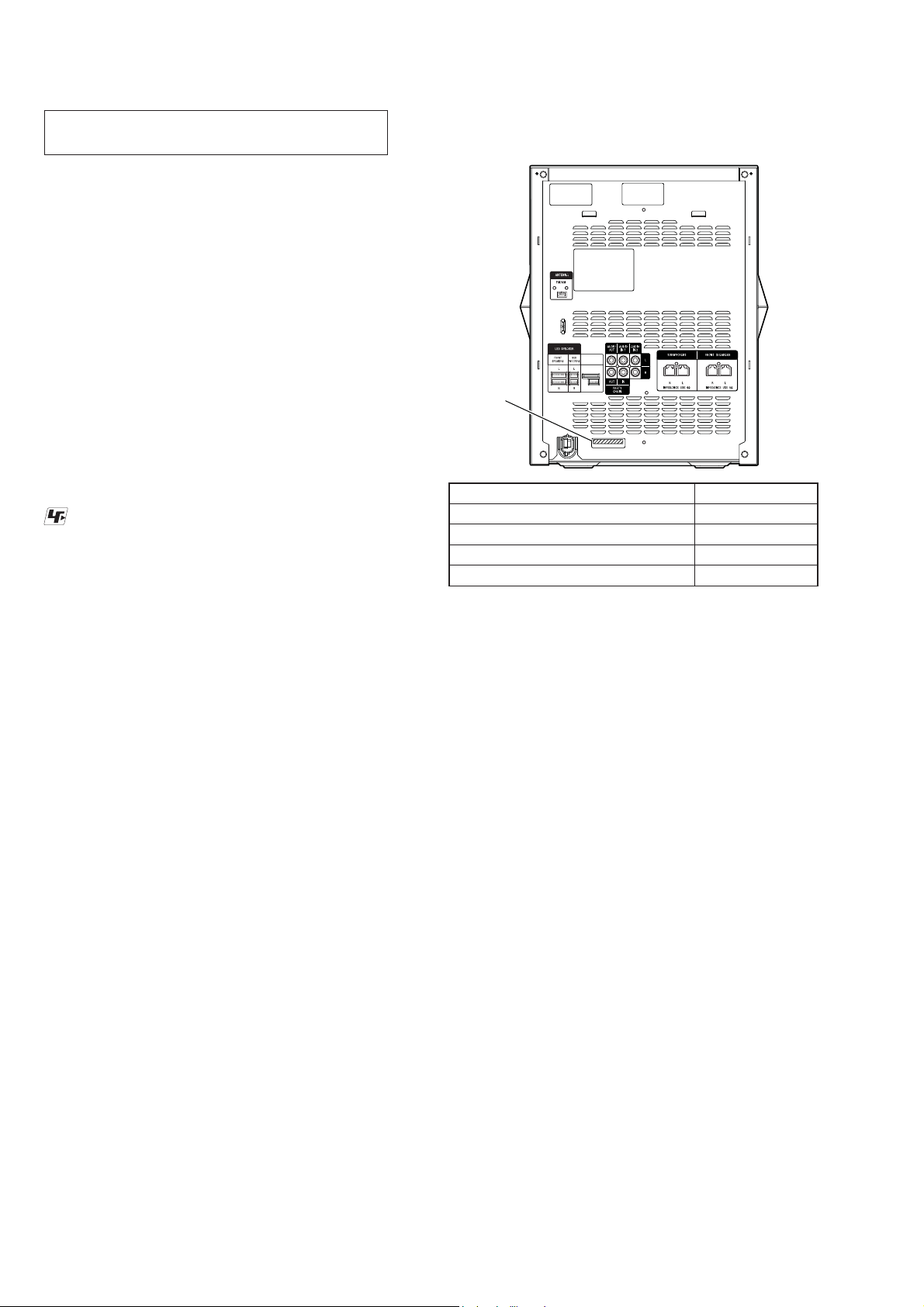
MODEL IDENTIFICATION
– Back Panel –
FOR SERVICE
USE
PART No.
Model Part No.
GPX888: E2, E51
GPX555: E2, E51, EA3, AUS, E4
US
Mexican
4-479-110-0[]
4-479-110-1[]
4-479-110-2[]
4-479-110-3[]
NOTE OF REPLACING THE IC001, IC002, IC106 AND
IC302 ON THE MB BOARD
IC001, IC002, IC106 and IC302 on the MB board cannot exchange
with single. When these parts on the MB board are damaged,
exchange the entire mounted board.
RELEASING THE DISC TRAY LOCK
The disc tray lock function for the antitheft of an demonstration
disc in the store is equipped.
Releasing Procedure:
1. Press [
\/1] button to turn the power on.
2. Press the [CD] button to select CD function.
3. While pressing the [x] button, press the [BASS BAZUCA]
button for more 5 seconds).
4. The message “UNLOCKED” is displayed and the disc tray is
unlocked.
Note: When “LOCKED” is displayed, the slot lock is not released by
turning power on/off with the
[\/1] button.
4

HOW TO OPEN THE TRAY WHEN POWER SWITCH TURN OFF
Note 1: After the side panel (L, R) and top panel is removed, this work is done.
Note 2: Please prepare the thin wire (clip etc. processed to the length of 8 cm or more).
1 Remove the panel, side (L, R) and panel, top.
(Illustration of disassembly is omitted.)
– Side view –
hole
Insert the clip etc. processed
to the length of 8 cm or
more in the hole on the
side of the chassis
and push.
CD drive
HCD-GPX555/GPX888
tray
3
8 cm or more
2 Insert the clip etc.
Push after it inserts it in this hole well.
Note:
tray
– Top view –
CAPACITOR DISCHARGE FOR ELECTRIC SHOCK PREVENTION
SMPS 3H401W BOARD (Conductor side view)
In checking the SMPS 3H401W board, make 3 capacitor discharge of C221, C602 and C618 for electrical shock prevention.
800 :/5 W
800 :/5 W
C618
C221
800 :/5 W
C602
5

HCD-GPX555/GPX888
NOTE OF REPLACING MB BOARD OR BLUETOOTH
MODULE OR RC-S801/A (WW) BOARD
When the MB board or BLUETOOTH module or RC-S801/A
(WW) board are replaced, please execute the below service mode.
Pairing this system with a
1. Press the [\/1] button to turn the power on.
2. Place the Bluetooth device within 1 meter (3 feet) from the
system.
3. Press BLUETOOTH on the unit to select Bluetooth function.
“BLUETOOTH” appears in the display panel.
4. Hold down BLUETOOTH on the unit for 2 seconds or more.
“PAIRING” fl ashes in the display panel.
5. Perform the pairing procedure on the Bluetooth device.
6. Select the model number of the unit on the display of the
Bluetooth device.
For example, select “SONY:MHC-GPX888” (or LBT-
GPX555/MHC-GPX555).
If passkey is required on the Bluetooth device, enter “0000”.
7. Perform the Bluetooth connection on the Bluetooth device.
8. When pairing is completed and the Bluetooth connection is
established, Bluetooth device name appears in the display
panel.
Depending on the Bluetooth device, connection may start
automatically after pairing is completed.
You can check the Bluetooth device address by pressing
DISPLAY repeatedly.
9. To cancel pairing operation, hold down BLUETOOTH on the
unit for 2 seconds or more until “BLUETOOTH” appears in
the display panel.
Bluetooth
device
Connecting with a smartphone by one touch (NFC)
Note: The operation in this mode must use a NFC-compatible smartphone
(Smartphones with a built-in NFC function [OS: Android 2.3.3 or
later, excluding Android 3.x])
1. Press the [\/1] button to turn the power on.
2. Download and install the app “NFC Easy Connect”.
Download the free Android app from Google Play by searching
for “NFC Easy Connect”.
3. Start the app “NFC Easy Connect” on the smartphone.
Make sure that the application screen is displayed.
4. Touch the smartphone to the N-Mark on the system until the
smartphone vibrates.
Playing music from a
For a Bluetooth device
1. Press the [
2. Press BLUETOOTH on the unit to select Bluetooth function.
“BLUETOOTH” appears in the display panel.
3. Establish connection with the Bluetooth device.
Press BLUETOOTH on the unit to connect to the last
connected Bluetooth device.
Perform the Bluetooth connection from the Bluetooth device if
the device is not connected.
Once the connection is established, the Bluetooth device name
appears in the display panel.
4. Press N.
Depending on the Bluetooth device,
– you may have to press N twice.
– you may need to start playback of an audio source on the
Bluetooth device.
For an NFC-compatible smartphone
1. Press the [\/1] button to turn the power on.
Touch the smartphone to the N-Mark on the system to establish
the Bluetooth connection.
Start playback of an audio source on the smartphone. For
details on playback, refer to the operating instructions of your
smartphone.
To disconnect the Bluetooth device
For a Bluetooth device
Press BLUETOOTH on the unit.
“BLUETOOTH” appears in the display panel.
For an NFC-compatible smartphone
Touch the smartphone to the N-Mark on the system again.
To erase all the pairing registration information perform
COLD RESET test mode (Refer page 13).
\/1] button to turn the power on.
Bluetooth
device
Complete the connection by following the instructions
displayed on the smartphone.
5. When pairing is completed and the Bluetooth connection is
established, the Bluetooth device name appears in the display
panel.
6

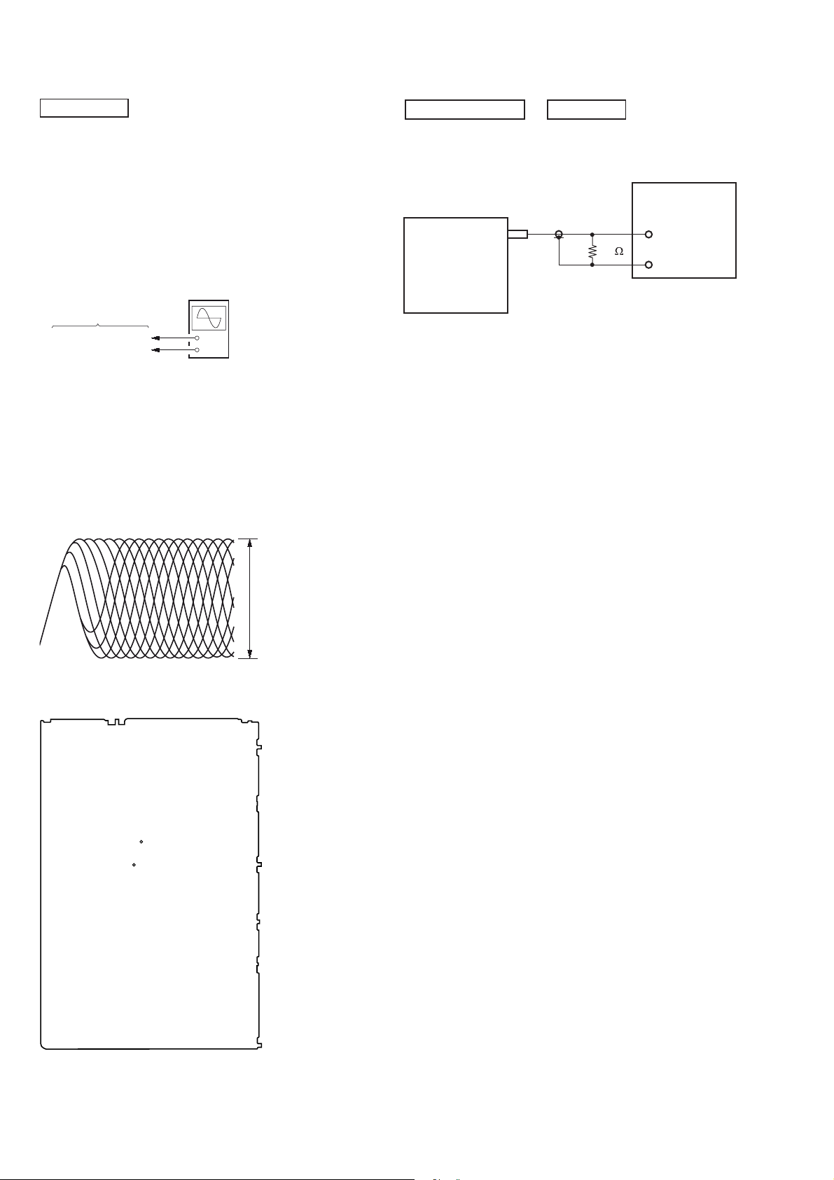
DISASSEMBLY
• This set can be disassembled in the order shown below.
2-1. DISASSEMBLY FLOW
SET
2-2. SIDE-L PANEL, SIDE-R PANEL,
TOP PANEL
(Page 8)
HCD-GPX555/GPX888
SECTION 2
2-3. LOADING PANEL
(Page 8)
2-4. FRONT PANEL SECTION
(Page 9)
2-5. CD MECHANISM SECTION
(CDM90-DVBU204//M)
(Page 9)
2-6. BACK PANEL SECTION
(Page 10)
2-7. MB BOARD, DAMP BOARD
(Page 10)
SWITCHING REGULATOR
2-8.
(3H401W)
(Page 11)
2-9.
SERVICE OPTICAL DEVICE,
WIRE (FLAT TYPE)
(Page 12)
7

HCD-GPX555/GPX888
Note: Follow the disassembly procedure in the numerical order given.
2-2. SIDE-L PANEL, SIDE-R PANEL, TOP PANEL
1 one screw
(+BVTP 3 u 10)
5 panel, side (L)
1 one screw
(+BVTP 3 u 10)
2 one screw
(+BVTP 3 u 10)
4 two claws
A
4 claw
qs four hooks
2 one screw
(+BVTP 3 u 10)
3
A
qa
B
qd panel, top
9 two claws
8
7 one screw
(+BVTP 3 u 10)
B
0 panel, side (R)
6 one screw
(+BVTP 3 u 10)
2-3. LOADING PANEL
– Side view –
Insert the clip etc. processed
to the length of 8 cm or
more in the hole on the
side of the chassis
and push.
8 cm or more
7 one screw
(+BVTP 3 u 10)
9 claw
6 one screw
(+BVTP 3 u 10)
3 three claws
4 panel, loading assy
hole
CD drive
2
1 Insert the clip etc.
Push after it inserts it in this hole well.
Note:
– Top view –
tray
8
2-4. FRONT PANEL SECTION
(GPX888)
7 CN601 (4P)
8 front panel section
HCD-GPX555/GPX888
2 two screws
(+BVTP 3 u 8)
6 CN451 (10P)
5 wire (flat type)
(10 core) (CN102)
(GPX555: US)
3 wire (flat type)
(8 core) (CN105)
1 one screw
(+BVTP 3 u 8)
4 wire (flat type)
(23 core) (CN109)
1 two screws
(+BVTP 3 u 8)
2-5. CD MECHANISM SECTION (CDM90-DVBU204//M)
7 three screws
(+BVTP 3 u 8)
9 CD mechanism section
(CDM90-DVBU204//M)
:LUHVHWWLQJ
Process so that lead wire does not
Note:
contact with fan.
8 holder, CDM
DJ KEYS board
(US, EA, AUS)
3 core, ferrite
2 cushion, saranet
(30 u 50)
5 wire (flat type)
(5 core) (CN303)
4 wire (flat type)
(24 core) (CN302)
1 CN401 (6P)
6 one screw
(+BVTP 3 u 8)
• Abbreviation
AUS : Australian model
EA : Saudi Arabia model
9

HCD-GPX555/GPX888
2-6. BACK PANEL SECTION
7 back panel section
2 four screws
(+BVTP 3 u 8)
3 one screw
(+BVTP 3 u 8)
5 holder, wire
6 sheet, service cover
4 one screw
(+BVTP 3 u 8)
1 wire (flat type)
(9 core) (CN851)
2-7. MB BOARD, DAMP BOARD
0 heat sink (GSX8)
9 sheet, thermal
qa three screws
(+BVTP 3 u 8)
qf DAMP board
3 wire (flat type)
(21 core) (CN111) (GPX888)
wire (flat type)
(19 core) (CN112) (GPX555)
qd bracket, heat sink
7 CN1000 (10P)
8 three screws
(+PTPWH 2.6 u L (DIA8.0))
qa one screw
(+BVTP 3 u 8)
4 one screw
(+BVTP 3 u 8)
4 four screws
(+BVTP 3 u 8)
5 MB board
qs
10
6 CN1001 (2P)
1 Remove the wires
from hooks.
2 CN001 (6P)
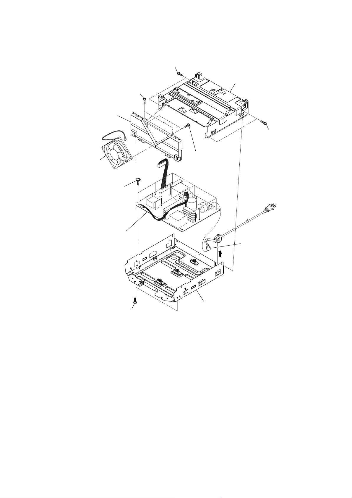
2-8. SWITCHING REGULATOR (3H401W)
6 two screws
(+BVTP 3 u 8)
1 two screws
(+BVTP 3 u 8)
4 bracket, fan
HCD-GPX555/GPX888
7 sub, chassis
6 two screws
(+BVTP 3 u 8)
5 DC fan
0 nine screws
(+PWH 3 u 8 (SUMITITE))
qa REGULATOR,
SWITCHING (3H401W)
2 two screws
(+BVTP 3 u 8)
3 two screws
(+BVTP 3 u 8)
8 CN1 (2P)
9
qs chassis assy
11

HCD-GPX555/GPX888
2-9. SERVICE OPTICAL DEVICE, WIRE (FLAT TYPE)
Note 1 : Before disconnecting the wire (fl at type) (24 core) of service optical device, solder the short-land.
8 four insulator screws
qs service,
optical device
3 Insert the thin
wire (clip etc.).
5 tray
1 six claws
qa insulator
6 belt
2 chuck holder assy (T)
qa insulator
qa insulator
0
9
qf wire (flat type)
(5 core)
qh holder, FFC
qj wire (flat type)
(24 core)
qg
7 connector
4
,QVWDOODWLRQRIZLUHIODWW\SHFRUHDQGZLUHIODWW\SHFRUH
This illustration sees the loading assy (T) from bottom side.
Note:
1 wire (flat type) (24 core)
loading assy (T)
terminal face
2 Through the hole
qd base, lo assy
5 two claws
3 Through the hole
Under the guide
(Fold area)
loading assy (T)
– Bottom view –
5 three claws
6 holder, FFC
4
7 wire (flat type)
(24 core)
8 wire (flat type)
(5 core)
12
Under the guide

SECTION 3
TEST MODE
HCD-GPX555/GPX888
[PANEL TEST MODE]
This mode is used to check the fl uorescent indicator tube, LEDs,
keys, [VOLUME / DJ CONTROL] jog, model, destination and
software version.
Procedure:
1. Press [OPTIONS] button and [FOOTBALL] button simultaneously and hold 3 seconds.
2. All LEDs and segments in fl uorescent indicator tube are light-
ed up. All RGB LEDs are lighted up in white color.
3. When you want to enter to the software version display mode,
press [+ / ] button.
The model information appears on the fl uorescent indicator
tube.
• “GNX5” is shown for XXX-GPX555.
• “GNX8” is shown for XXX-GPX888.
Press [+ / ] button again to view the destination informa-
tion.
4. During the destination information display, press [+ / ] button. Each time [+ / ] button is pressed, the fl uorescent indi-
cator tube shows the version of each category software in the
following sequence: SC, MTK, OPU, UI, PF, SYS, CD, CDMA,
CDMB, ST, TA, TM, and return back to model information display.
5. When [] button is pressed while the version numbers
are being displayed except model and destination, the
date of the software creation appears. When [] button
is pressed again, the display returns to the software version display.
6. Press [- / ] button, the key check mode is activated.
7. In the key check mode, the fl uorescent indicator tube displays
“K 0 V0”.
• Each time a button is pressed, “K” value increases.
However, once a button has been pressed, it is no
longer taken into account.
• “V” value increases in the manner of 0, 1, 2, 3... if
[VOLUME] knob is turned clockwise, or it decreases
in the manner of 0, 9, 8, 7... if [VOLUME] knob is
turned counterclockwise.
8. When [ENTER] button is pressed after all LEDs and segments
in fl uorescent indicator tube light up, alternate segments in
fl uorescent indicator tube and LEDs would light up, all RGB
LEDs would light up in red color. If you press [ENTER]
button again, another half of alternate segments in fl uorescent
indicator tube and LEDs would light up, all RGB LEDs would
light up in green color. Pressing [ENTER] button again would
cause all segments in fl uorescent indicator tube and LEDs
light up, all RGB LEDs would light up in blue color. Pressing
[ENTER] button again would turn off all segments in fl uores-
cent indicator tube and all LEDs including RGB LEDs.
9. To release from this mode, press the buttons in the same
manner as step 1, or disconnect the power cord.
[COLD RESET]
The cold reset clears all data including preset data stored in the
data fl ash to initial conditions included history mode data. Execute
this mode when returning the set to the customer.
Procedure:
1. Press [\/1] button to turn on the system.
2. Press [] button and [PAN] button simultaneously for 3
seconds.
3. “COLD RESET” appears on the fl uorescent indicator tube.
After that, the fl uorescent indicator tube becomes blank for a
while, and the system is reset.
[CD TRAY LOCK MODE]
This mode let you lock the disc tray. When this mode is activated,
the disc tray will not open when [OPEN/CLOSE] button is pressed.
The message “LOCKED” will be displayed on the fl uorescent
indicator tube. This mode only applied when there is disc(s) on
the tray.
Procedure:
1. Press [\/1] button to turn on the system.
2. Select CD function.
3. Press [] button and [BASS BAZUCA] button simultaneously
and hold down until “LOCKED” or “UNLOCKED” displayed
on the fl uorescent indicator tube (around 5 seconds).
[USER RESET]
The user reset clears all data including preset data stored in the data
fl ash to initial conditions exclude history mode data.
Procedure:
1. Press [
2. Press [] button and [MOVIE/GAME] button simultaneously
3. “RESET” appears on the fl uorescent indicator tube. After that,
\/1] button to turn on the system.
for 3 seconds.
the fl uorescent indicator tube becomes blank for a while, and
the system is reset.
13

HCD-GPX555/GPX888
[HISTORY MODE]
This mode is used to check important data stored in the system
when PROTECTOR happen.
Procedure:
1. During demo mode, press [OPTIONS] button and [FLANGER]
for 5 seconds to mode in to history mode.
Press the [M > / TUNING+] or [ .m / TUNING-]
2.
button to check history data stored.
Display on fl uorescent indicator tube Description
PROCOUNT
PROTYPE
T1
T2
FUNC
VOL
ATT
EQ LOW
EQ MI D
EQ H I GH
SW
SURR
DJ
BAZUCA
※※※※※H※※
※※※※※H※※
※※※※※※※
※※※※※※ ※※
※※
※※※※
※※※
※※※
※※※
※※※
※※※
※※※
※※※
※※※
Protector Count
Protector Type (refer to Protect Type Description)
Single Power On
M
Total Power On
M
Input Function
Volume
Actual Attenuation
Low EQ Level
Mid EQ Level
High EQ Level
Subwoofer Setting
Surround Setting
DJ Effect Setting
Bass Bazuca Setting
To release from this mode, press [\/1] button.
Protect Type Description:
Error Code Description
E01 The over current condition to MOSFET occurs
by defect of MOSFET or defect of PS output
line.
E03 Defect of power supply circuit to AMP.
There is possibility of unusual power supply of
any of the AMP IC or Pre-amplifi er.
E04 DC appears in SP terminal by defect of AMP
IC and MOSFET
or
Defect of DC FAN and DC FAN driver circuit.
E05 Unusual heat up of MOSFET by improper
assembly of heat sink, destruction of MOSFET
etc.
If speaker does not have output even if the set status is not in
PROTECT mode, the following defect might be possible:
Defects Possible cause
RESET defect Reset signal status from micom is not ‘H’.
14
[MODEL & DEST WRITE MODE]
This mode is used to set software model & destination.
This mode only available when no permanent model & destination
is stored.
Procedure:
1. Press [MOVIE/GAME] button & [LED PATTERN] button
simultaneously and hold for 5 seconds.
2. Fluorescent indicator tube display will show “M XXXXX”.
3. Press [/+] / [-/] button to select the model based on the
set’s model.
Product Code F. Tube display
HCD-GPX555 “M GNX5”
HCD-GPX888 “M GNX8”
4. Press [ENTER] button.
5. Fluorescent indicator tube display will show “D XXXXX”.
6. Press [/+] / [-/] button to select the destination based
on the set’s country.
Area Code Country F. Tube display
J1 Japan “D J”
JE1 Tourist “D JE”
U2/CA2 America, Canada “D NA”
CEL/CE1/
CE2
CEK U.K. “D CEK”
RU1/RU3 Russia “D RU”
AU1 Australia “D AU”
CN1 China “D CN”
E12 India, Pakistan, Morocco “D E12”
E3/E15 Middle East, Iran “D E3”
E4/ EA3/
E93/ SA2
HK1/
HK2/PL1/
SP1/SP2/
SP6/TH1
KR2 Korea “D KR”
TW2 Taiwan “D TW”
E2, E32,
E51, AR2
BR1 Brazil “D BR”
MX2,
MX4
Europe(general) “D CE2”
Saudi Arabia, Africa “D EA3”
Hong Kong, Philippines,
Singapore, Malaysia,
Thailand
Latin America(general),
Chile, Peru, Argentina
Mexico “D MX”
“D ASIA”
“D LATIN”
HCD-GPX555/GPX888
7. Press [ENTER] button to confi rm the selection.
8. “RESET” appears on the fl uorescent indicator tube. After that,
the fl uorescent indicator tube becomes blank for a while, and
the system is reset.
9. Mode in [PANEL TEST MODE] again to confi rm on the
model & destination.
15
HCD-GPX555/GPX888
SECTION 4
ELECTRICAL CHECK
CD SECTION
Note:
1. CD Block is basically constructed to operate without adjustment.
2. Use YEDS-18 disc (Part No. 3-702-101-01) unless otherwise indicated.
3. Use an oscilloscope with more than 10 MΩ impedance.
4. Clean the object lens by an applicator with neutral detergent when the
signal level is low than specifi ed value with the following checks.
5. Check the focus bias check when optical pick-up block is replaced.
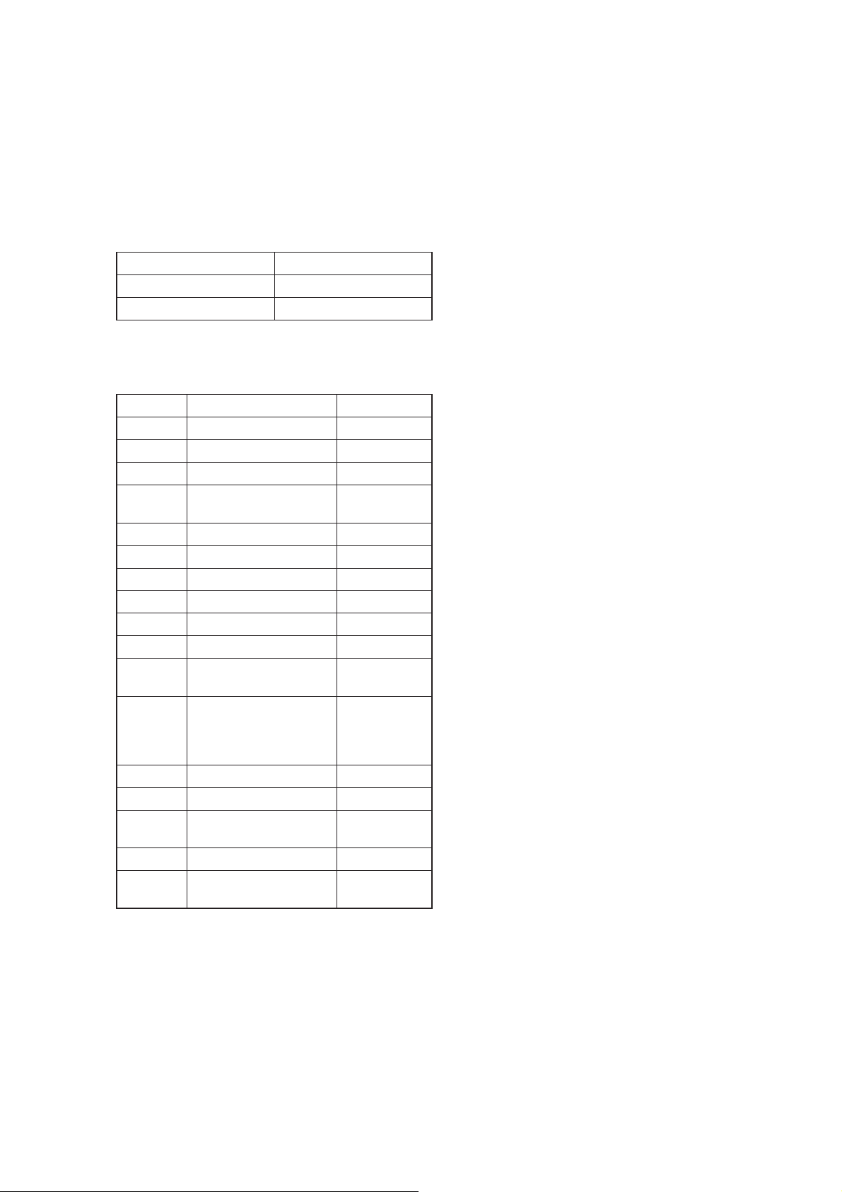
FOCUS BIAS CHECK
oscilloscope
(DC range)
MB board
JL317 (RF Signal)
JL312 (Vc/Reference)
+
–
Procedure :
1. Connect the oscilloscope to JL317 (RF Signal) and JL312 (Vc/
Reference) on the MB board.
2. Press the [
STANDBY] button to turn the power on, and
?/1
press the [CD] button to select CD function.
3. Set disc (YEDS-18) and press the [u] button to playback.
4. Confi rm that oscilloscope waveform is as shown in the fi gure
below (eye pattern).
A good eye pattern means that the diamond shape () in the
center of the waveform can be clearly distinguished.
VOLT/DIV: 200 mV
TIME/DIV: 500 ns
level:
1.0 ± 0.25 Vp-p (CD)
TUNER SECTION
0 dB = 1 μV
FM AUTO STOP CHECK
signal
generator
set
+
75
–
Procedure:
1. Turn the power on.
2. Input the following signal from Signal Generator to FM antenna input directly.
Carrier frequency : A = 87.5 MHz, B = 98 MHz, C = 108 MHz
Deviation : 75 kHz
Modulation : 1 kHz
ANT input : 35 dBu (EMF)
Note: Please use 75 ohm “coaxial cable” to connect SG and the
set. You cannot use video cable for checking.
Please use SG whose output impedance is 75 ohm.
3. Set to FM tuner function and scan the input FM signal with
automatic scanning.
4. Confi rm that input Frequency of A, B and C detected and
automatic scanning stops.
The stop of automatic scanning means “The station signal is
received in good condition”.
Checking Location:
-MB Board (Conductor Side)-
JL317
JL312
16

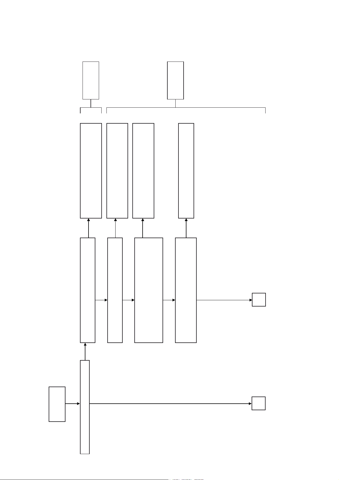
SECTION 5
TROUBLESHOOTING
Checks whether the state of a Cable and Outlet are normal.
If there are no problems, checks circumference circuit for
Main on/Sub on Output of Main mount side.
Replaces Switching regulator if it is not up to standard.
HCD-GPX555/GPX888
No
Yes
AC IN
The Output from Switching regulator is checked.
Is following power voltage up to standard?
(4)
The Power Control signal to Switching regulator is checked.
Is following power voltage OK?
Main on/Sub on Standby Demo mode Power On
CN 3 : pin6 Low (0V) Low (0V) Hi (3.3V)
(6)
Standby Demo mode Power On
No
0.5V
±
0.5V 13V
±
0.5V 13V
±
CN3 pin1 13V
5%
±
0V 61V
0V
CN2 pin10
2.5V
±
0V 24V
0V
pin7
2.5V
±
0V -24V
0V
pin5
5%
±
0V -61V
0V
pin4
0V 16-23V
Yes
END
0V
pin1
(3)
Switching Regulator Diagnosis Flow
(5)
(2)
(1)
pin1-2: 13V
pin3-4: GND
(1) AC input
(2) Fuse
(3) Sub Power transformer
(4) CN3 Connector
pin5: AC-DET
pin6: MAIN-ON
(5) MAIN Power transformer
(6) CN 2 Connector
pin1 : V3+(DC+16-23V)_(ref-V1)
pin2-4 : V1-(DC-61V)
pin5 : V2-(DC-24V)
pin6 : GND
pin7 : V2+(DC+24V)
pin8-10 : V1+(DC+61V)
17

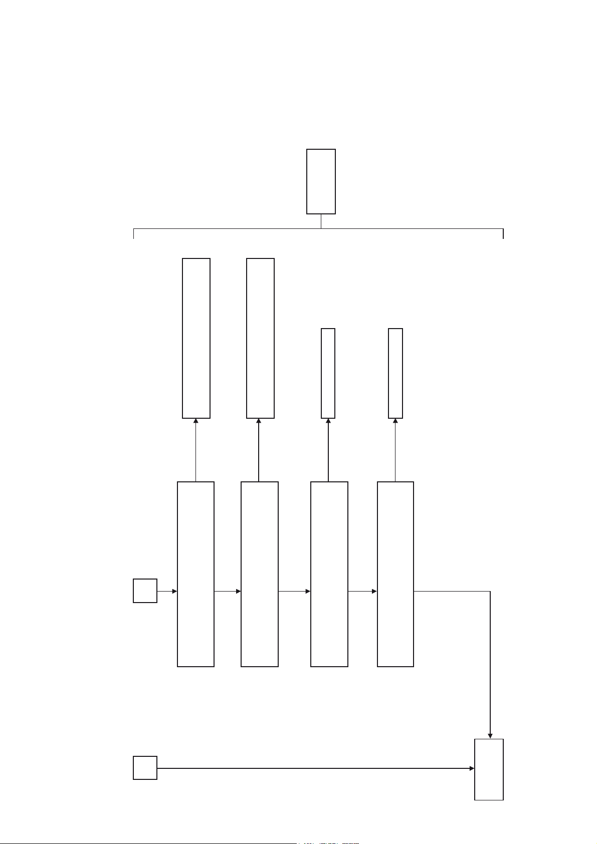
HCD-GPX555/GPX888
Checks IC303 circumference circuit for +1.2V.
Check IC002 (JL040) circumference circuit for +3.3V.
No
Checks CL335 for +3.3V and +1.2V REG IC303.
Does it output the power voltage of 3.3V and 1.2V?
No
Checks circumference circuit for SL+/SL- of IC401.
Checks circumference circuit of IC301 FMO Signal.
No
Yes
Yes
Does it output the signal?
Checks CN401 SL+/SL- signal.
The Sled motor has a problem.
Replaces BU.
Checks circumference circuit of IC301 DMO Signal.
Checks circumference circuit for SP+/SP of IC401.
No
Does it output the signal?
Checks CN401 SP+/SP- signal.
No
Checks circumference circuit of IC301 FOO Signal.
Checks circumference circuit for FCS+/FCS- of IC401
No
Yes
The Spindle motor has a problem.
Replaces BU.
Yes
Does it output the signal?
Checks CN302 FCS+/FCS- signal.
No
The Optical pickup has a problem.
Replaces BU.
Yes
REMOVE TOP PANEL
TURN ON
TRAY IN
Does Optical pickup move to inner circumference?
Optical Block Diagnosis Flow (1/2)
(Visual check)
18
Yes
Does Spindle motor rotate?
(Visual check)
Yes
Does Optical pickup do focus search?
(Visual check)
A

HCD-GPX555/GPX888
Checks circumference circuit of Q402.
Checks circumference circuit of IC301 LD01.
No
Yes
The Optical pickup has a problems.
Does it output 2V when laser become luminous?
Checks JL306 (LD780) signal.
No
Replaces BU.
If it is not up to standard,
No
Replaces BU if it is not up to standard.
No
Yes
Lens cleaning is performed.
Is output level of RF signal (JL317) up to standard?
Yes
RF Level = 1.05 ±0.45 Vpp
Test CD:YEDS-18
No
The Optical pickup has a problems.
Replaces BU.
A
Optical Block Diagnosis Flow (2/2)
Yes
Does laser diode become luminous ?
(Visual check)
Yes
DISC IN
Yes
Test CD:YEDS-18
Is output level of RF signal (JL317) up to standard?
RF Level = 1.05 ±0.45 Vpp
Yes
Confirms that there is no sound skip.
Is there no problem with Long term Aging Test (60min)?
END
19
HCD-GPX555/GPX888
MB Board
Reinserts the cable or Exchanges.
If there are no problems, checks output of
Switching Regulator Board.
Reinserts the cable or Exchanges.
If there are no problems, checks output of
Main ON of MB Board side.
Reinserts the cable or Exchanges.
If there are no problems, checks output of
Switching Regulator Board.
No
No
No
DAMP Board
Checks circumference circuit of REG IC1002.
If there are no problems, exchanges IC1002.
No
Yes
Checks 13V output of CN001 1pin(Main ON).
Is the power voltage OK?
No
Yes
PLAY MUSIC
DAMP/MB Mount Diagnosis Flow (1/2)
Is there audio output from DAMP Board?
Checks 3V output of CN001 6pin(Main ON).
Yes
Yes
Is the power voltage OK?
Checks 62.5V output of CN1000 10pin (+VH),
-62.5V output of CN1000 2pin (-VH) and -49V
output of CN1000 1pin (-49V).
Is the power voltage OK?
Yes
Checks OUT terminal -50.5V output of REG IC1002
Yes
Or, checks GND and OUT Terminal with Tester.
Is it shorted out?
B
A
20
DAMP Board
HCD-GPX555/GPX888
Checks circumference circuit of REG IC1000.
If there are no problems, exchanges IC1000.
No
B
Checks OUT Terminal 5V output of REG IC1000 or,
checks GND and OUT Terminal with Tester.
Is it shorted out?
Checks circumference circuit of REG IC1001.
If there are no problems, exchanges IC1001.
No
Yes
Checks OUT Terminal -5V output of REG IC1001 or,
Yes
checks GND and OUT Terminal with Tester.
Is it shorted out?
Replaces DAMP Board
No
Leave DAMP to a state of it only and, checks
Power Audio Driver (MOSFET) with Tester.
Replaces DAMP Board
No
Yes
Is it shorted out? (Refer to Page 22.)
Assembles into the unit again then, checks
Yes
whether there is the audio output from
DAMP Board.
A
DAMP/MB Mount Diagnosis Flow (2/2)
END
21

HCD-GPX555/GPX888
Ver. 1.1
CL1064
¾
CL1065
ÚGPX555
¾GPX888
MOSFET Confi rmation for DAMP Mount
C1526
CL1035
CL1034
CL1033
C1125
C1126
CL1029
C1122
C1112
CL1027
CL1028
C1164
C1163
C1160
C1157
CL1026
R1232
R1228
CL1063
R1253
CL1066
R1260
Tes te r Tes te r
CL1032
C1178C1184
R1227
CL1105
CL1106
R1263
CL1103
Tester
C1224C1232
CL1104
Tester
C1169
C1183
R1212
CL1107
CL1045
CL1042
C1182
C1191
C1223
C1237
R1275
CL1046
CL1050
CL1047
C1234
C1240
R1723
Ú
CL1036
C1180
C1190
R1234
C1236
C1239
R1286
R1197
CL1043
C1192
CL1044
R1213
R1223
R1237
CL1080
R1244
CL1048
C1241
R1278
CL1049
R1284
R1289
Tes te r
C1329
C1335
CL1020
C1323
C1325
CL1021
C1374
CL1022
C1369
C1363
C1362
CL1023
CL1069
R1326
¾
R1359
CL1072
Tes te r
C1255
R1330
CL1102
¾
CL1101
C1260
R1363
C1302
CL1099
CL1100
C1310
Tester
C1525
Tes te r
CL1108
CL1110
R1700
CL1071
R1699
C1517
C1247
C1259
CL1055
C1258
¾
C1268
C1303
C1314
CL1060
C1312
C1317
C1257
R1308
CL1053
C1267
CL1051
CL1052
R1333
¾
R1374
C1316
CL1056
CL1058
CL1057
R1385
R1294
C1269
CL1054
R1313
R1336
R1321
CL1090
C1313
R1350
C1318
R1376
CL1059
R1557
R1388
R1382
R1675
R1682
CL1012
R1681
CL1016
CL1013
CL1015
CL1014
CL1062
CL1061
R1316
R1208
CL1075
R1199
C1166
R1646
CL1074
CL1070
C1209
R1591
CL1079
R1250
R1271
R1352
CL1068
R1604
R1305
CL1085
R1296
C1243
R1592
CL1084
CL1083
CL1088
R1594
C1285
R1351
CL1089
R1372
R1609
CL1009
CL1007
CL1040
R1597
CL1041
R1601
CL1039
C1490 C1488
R1602
R1598
CL1038
CL1037
R1636
R1617
C1502
C1504
R1618
R1614
CL1008
CL1001
CL1006
CL1019
CL1067
CL1073
C1026
CL1010
CL1003
CL1002
CL1011
CL1004
CL1109
CL1005
CL1082
<Note>
Please check each channel’s resistance value for the Coil’s terminal and Capacitor’s + and – terminal.
These terminal is equal to resistance value for POWER AUDIO DRIVER terminal.
22
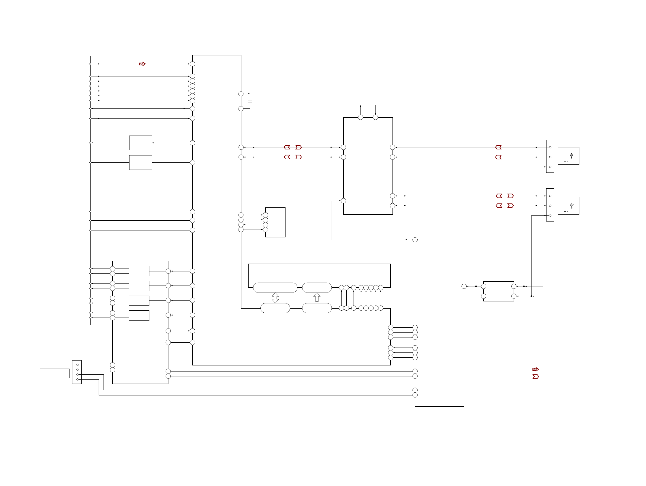
6-1. BLOCK DIAGRAM - RS SERVO, USB Section -
HCD-GPX555/GPX888
SECTION 6
DIAGRAMS
92$$
92%%
92&&
92''
'(9,&(237,&$/
&0665)6*
/2'9'+,&'06:
95
95
5)
9&
3'
$872
32:(5&75/
4
$872
32:(5&75/
4
5),3
5)B&
5)B%
5)B$
5)B'
5)B)92((*
5)B(92))+
9
0',
/'2/'
/'2/'
&'5)$03
)2&8675$&.,1*(5525$03
&'6<67(0352&(6625
',*,7$/6(592352&(6625
,&
06:
&'B95
'9'B95
;7$/2
;7$/,
86%B'0
86%B'3
6)B&6
6)B'2
6)B',
6)B&.
;
0+]
'0
'3
((3520
,&
B&6
62
6,
6&.
86%&21752//(5
5(6(7
;
0+]
;
,&
;
&1
'3
'0
'3
'0
'$
'$
9%86
'%
'%
9%86
&1
3/$<
A
9 P$
5(&3/$<
B
9 P$
+8%5(6(7
&211(&772
06%2$5'
)&6
)&6±
75.
75.±
6/
6/±
63
63±
&1
/2$'
/2$'
75$<,1
75$<287
&+6<67(0
02725'5,9(5
,&
9275
9275
)2&86
&2,/'5,9(5
)2&86
&2,/'5,9(5
)2&86
&2,/'5,9(5
)2&86
&2,/'5,9(5
%,$6
087(
):'
5(9
)22
'*'4±'4
'02
)02
752
995()
087(
±±
5'±5'
06'5$0
,&
$±$
±
±
5$±5$
6<67(0
&21752//(5
,&
%$ %$
%$ %$
5&/. &/.
'40 /'40
'40 8'40
5$6 5$6
&$6 &$6
5:( :(
,)6',
,)6'2
,)6&.
3567
,)&6
,)%6<
07.6'2
07.6',
07.&/.
07.5(6(7
07.;,)&6
07.%86<
86%2&
&203$5$725
86%
,&
86%$9
86%%9
6LJQDOSDWK
&'02725
&'02725
&'3/$<
86%
5FKLVRPLWWHGGXHWR
&'0/2$'6:
&'081/2$'6:
VDPHDV/FK
HCD-GPX555/GPX888
2323
HCD-GPX555/GPX888
6-2. BLOCK DIAGRAM - MAIN Section -
ANTENNA
FM/AM
AUDIO
IN 1
J602 (1/2)
CN3000
2
3
GPX888
MIC IN
J2300
PARTY
R
L
AUDIO IN 2
CHAIN IN
R-CH
RL
FM DRIVER
(FM RECEIVER)
IC3000
413
ARF1 L OUT
R OUT
12
ARF2
5
R-CH
SIGNAL SELECTOR
IC605
Y0
1
X3
11
Y3
4
X1
14
X2
15
B
9A10
ANALOG
SELECTOR
Q604
MIC AMP
IC2300
RV2600
MIC LEVEL
MIN MAX
13
X
1375
MIC DETECT
Q2300, Q2301
112
117
ACLK
ALRCK
113
ABCK
106
ADIN
118
ASDATA0
CD RF AMP
FOCUS/TRACKING ERROR AMP
CD SYSTEM PROCESSOR
DIGITAL SERVO PROCESSOR
IC301
(2/2)
X103
12.288MHz
STEREO A/D
CONVERTER
IC609
VINL
13
VINR
14
STEREO A/D
CONVERTER
VINL
13
SCKI
6
LRCK
7
BCK
8
A
1
SIGNAL SELECTOR
IC607
X102
13.333MHz
IC606
9
2
B
DOUT
BCK
DOUT
Y
5
8
9
X101
32.768kHz
STEREO A/D
CONVERTER
IC604
LRCKI
6
BCKI
5
SDIN
4
ASYNCHRONOUS
SAMPLE RATE
CONVERTER
IC610
VOUTL
VOUTR
DATA
BCK
LRCK
BCKO
LRCKO
SDOUT
AUDIO
L
OUT
OP AMP
+
3
+
5
ANALOG
SELECTOR
Q611
IC601
J602 (2/2)
OUT
OUT
1
7
MUTE
PROTECT
Q602
MUTE SW
Q606
SIGNAL
SELECTOR
4
11
1
12
VOUTL
VOUTR
VOUTL
VOUTR
IC602
Y3
Y
3
X3
X
13
Y0
A
10
X0
B
9
7
8
R-CH
7
8
R-CH
ANALOG
SELECTOR
Q605, Q607
OP AMP
IC603
+
OUT
7
8
2
1
3
25
24
23
3
5
1
+
OUT
7
STEREO D/A
CONVERTER
IC611
BCK
1
DATA
2
STEREO D/A
CONVERTER
IC615
BCK
1
DATA
2
R
MUTE SW
Q603
PARTY
CHAIN OUT
FRONT-L
>001B
AMP SECTION
(Page 25)
SW-L
X3000
12MHz
HCD-GPX555/GPX888
BLUETOOTH
16
17
X1
X2
CN102
4
5
9
8
IIC/RDSI
BT-RXD
BT-TXD
BT-RESET
3.3V
41
42
ANALOG-ASEL
ANALOG-BSEL
DA
11
CK
8
6
128
ST-DATA
127
ST-CLK
114
ST-RDS
BUS BUFFER
IC102 (1/2)
BLUETOOTH
POWER CONTROL
Q103, Q104
65
173
BT-RXD(MD-CLK)
65
133
MIC-DETECT
BT-RESET
BT-ON
BT-TXD
5
8
91 92
AUDIO-X1
70 71 68 67
AUDIO-X2
EXTAL
SYSTEM CONTROLLER
XTAL
IC101 (2/4)
RTC-X2
RTC-X1
CP-DATA
126
2
SDA
EPROM
IC105
125
6
CP-CLK
SCL
28
SSI3_DI
26
24
27
SSI3_BCKO
SSI3_LRCKO
32
55
59
SSI1_DI
LINK-DET
SSI3_DOUT3
4)ODVK&6
4)ODVK6,2
169
172
1
2
CS
SO/SIO1
EPROM
29
SSI0_DO
4)ODVK6,2
4)ODVK6,2
166
170
168
3
5
SI/SIO0
W P/SIO2
IC106
33
SSI2_DO
SSI0_BCKO
4)ODVK&/.
4)ODVK6,2
167
6
7
SCLK
HOLD/SIO3
LINK-OUT-B
LINK-OUT-A
/LINE-MUTE-FR
LINK-SET
51
176
96
175
6LJQDOSDWK
: AUDIO
: TUNER (FM/AM)
: CD PLAY
: MIC
5FKLVRPLWWHGGXHWR
VDPHDV/FK
2424

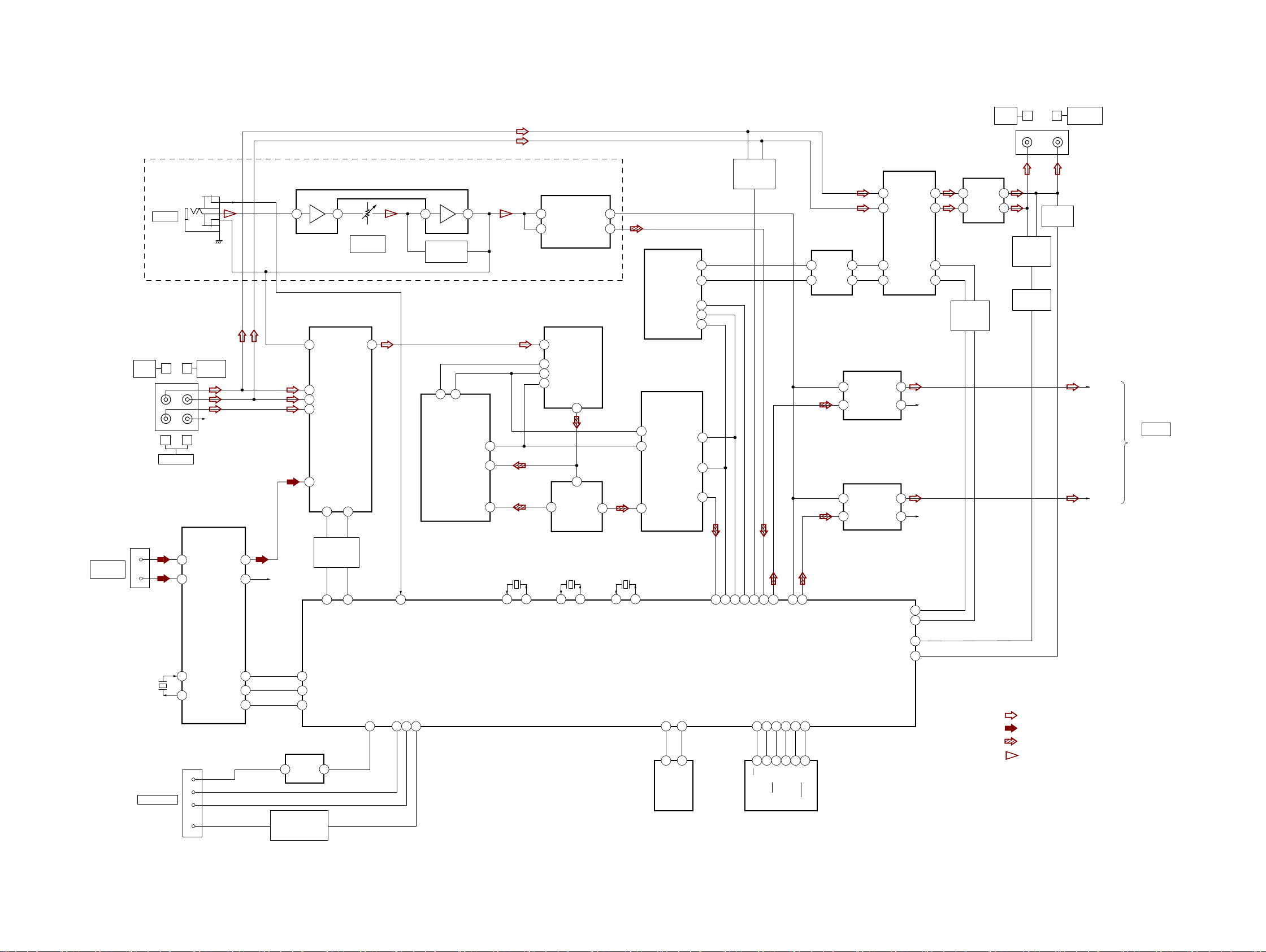
6-3. BLOCK DIAGRAM - AMP Section -
HCD-GPX555/GPX888
>001B
MAIN SECTION
(Page 24)
FRONT-L
SWL-L
R-CH
R-CH
OP AMP
IC1015
OP AMP
IC612
+
3
+
5
OP AMP
+
3
+
5
IC616
OUT
OUT
OUT
OUT
1
7
MUTE
PROTECTION
Q1035
GPX888
MUTE
PROTECTION
Q1042
1
7
+IN_1
3
+IN_2
5
OP AMP
IC1016
+IN_1
3
+IN_2
5
DUAL
OPERATIONAL
AMPLIFIER
IC1003
5
OUT_1
OUT_2
OUT_1
OUT_2
1
RESET
SWITCH
Q1026
7
1
RESET
SWITCH
Q1031
GPX888
7
RESET
SWITCH
Q1036
1
7
RESET
SWITCH
Q1041
POWER AMP
3
IN
CSD
5
POWER AMP
3
IN
CSD
5
POWER AMP
3
IN
CSD
5
POWER AMP
3
IN
CSD
5
IC1009
IC1011
IC1012
IC1014
COM
COM
COM
COM
+63V
14
HO
13
VS
11
LO
10
14
HO
13
VS
11
LO
10
14
HO
13
VS
11
LO
10
14
HO
13
VS
11
LO
10
DIGITAL AUDIO MOSFET
Q1023
DIGITAL AUDIO MOSFET
Q1025
-63V
+63V
DIGITAL AUDIO MOSFET
Q1028
DIGITAL AUDIO MOSFET
Q1030
-63V
+63V
DIGITAL AUDIO MOSFET
Q1032
DIGITAL AUDIO MOSFET
Q1034
-63V
+63V
DIGITAL AUDIO MOSFET
Q1038
DIGITAL AUDIO MOSFET
Q1039
-63V
TH1007 D1024
TH1008 D1024
TH1009 D1034
TH1010 D1034
DC DETECT
SWITCH
Q1027
DC DETECT
SWITCH
Q1037
PGND
FL
FR
PGND
PGND
SWL
SWR
PGND
PGND
SWR
TH-PROTECT
TB1000
TB1001
TB1002
AMP SECTION
FL+
FR+
-
L
+
-
R
+
-
L
+
-
R
+
-
+
,03('$1&(86(
>002B
(Page 26)
FRONT SPEAKERS
,03('$1&(86(
SUBWOOFER
,03('$1&(86(
SUBWOOFER
GPX888
GPX555
HCD-GPX555/GPX888
MUTE
SWITCH
Q109
96
/LINE-MUTE-FR
136
AMP-CLK-FR
AMP RESET
SWITCH
Q1008
120
/AMP-RESET
AMP
SWITCH
Q1058
131
/AMP-SD
SYSTEM CONTROLLER
IC101 (3/4)
THERMISTOR
PROTECTION
Q1067, Q1071
78
THERMISTOR-PROTECT
DC DETECT
SWITCH
Q1060
132
/DC-DET
D1011
FAN RESET
SWITCH
/AMP-RESET
INT- FAN-D ET
Q1073
120
6LJQDOSDWK
13V
: AUDIO
5FKLVRPLWWHGGXHWR
VDPHDV/FK
FAN DRIVER
Q1072
CN1001
DC FAN
FAN PROTECTION
82
(LOCK)
Q1075
2525

HCD-GPX555/GPX888
Ver. 1.1
6-4. BLOCK DIAGRAM - PANEL/POWER SUPPLY Section -
GPX555
LED SPEAKER
FRONT
SPEAKERS
GPX888
LED SPEAKER
FRONT
SPEAKERS
LED
SPEAKER
SUBWOOFERS
VACUUM
FLUORESCENT
DISPLAY
ND2000
D2000, D2002,
D2003, D2005,
D2011, D2200,
D2205
D2006 ~ D2010
CN501
2
L
3
4
CN502
2
R
3
4
CN505
6
7
8
L
2
3
4
CN506
2
3
4
R
6
7
8
CN503
2
L
3
4
CN504
2
R
3
4
VOLUME /
DJ CONTROL
S2200 ~ S2212
S2000 ~ S2009, S2100
S2100
OUT0
5 - 205 - 19
OUT15
OUT0
OUT15
16 - 18
13 - 15
10 - 12
5 - 7
18- 20
15 - 17
12 - 14
35
SI
36
CLK
37
LAT
38
BK
REMOTE CONTROL
LED DRIVE
IC2000
I
TRANS
PWMCLK
SOUT
LED DRIVE
IC2002
I
TRANS
PWMCLK
LED SELECTOR
IC502
PWMCLK
/OUT13
I
/OUT11
/OUT10
I
/OUT8
/OUT7
I
/OUT5
/OUT2
I
/OUT0
LED SELECTOR
IC501
/OUT15
I
/OUT13
PWMCLK
/OUT12
I
/OUT10
/OUT9
I
/OUT7
RECEIVER
SIN
SCK
SIN
SCK
SIN
SCK
TRANS
SOUT
SIN
SCK
TRANS
IC2100
S2101
ROTARY
ENCODER
2
3
4
21
22
2
3
4
21
2
3
21
4
22
2
3
21
4
FL-SOUT
40
FL-CLK
35
FL-LATCH
38
FL-BK
134
135
SIRCS
83
MASTER-VOLUME
AD-KEY1
85
AD-KEY0
84
POWER-KEY
45
SYSTEM CONTROLLER
IC101 (5/5)
RGB-SOUT
48
RGB-SCLK
137
RGB-PWM-CLK
118
RGB-TRANS-LED-SPK/SD_WP_0
112
PCONT-PSAVE-PROTECT
THERMISTOR-PROTECT
SPM-C-MON
PCONT-DAMP
PCONT-BTSTBY
RES
C-CONT
VBUS-OE
AC-CUT(MD-BOOT0)
MTK-POWER-CTRL
SPM-AMBIENT-TEMP
79
117
56
76
165
12
63
164
57
80
78
TD FL
TUBE
+1.2V
TH571
+1.2V REG.
1 8
IC303
LED+5.2V
D2004, D2012,
D2030 ~ D2031
+3.3V
+5V
D+3.3V
5.2V
USB+5V
+5V REG.
5 4
IC3001
POWER CONTROL
PROTECTION
Q006
POWER CONTROL
PROTECTION
Q007
POWER CONTROL
PROTECTION
Q009
POWER CONTROL
PROTECTION
Q008
VOLTAGE
4 2
DETECTOR
IC103
POWER CONTROL
PROTECTION
Q005
POWER CONTROL
PROTECTION
Q001
POWER CONTROL
PROTECTION
Q002
DC-DC CONVERTER
TRANSFORMER
T2000
+5V REG.
IC006
+9V
+3.3V
SWITCHING
TRANSISTOR
Q2000 ~ Q2001
+1.2V SW1
VOLTAGE REGULATOR
IC001
SW2
14
SW1
3
EN2
12
SW1
5
+9V REG.
IC004
VIN1
VIN2
PROTECTION CONTROL
+3.3V REG.
IC002
VIN1
3
SW2
14
1
16
1
VIN2
16
POWER
CONTROL
PROTECTION
Q004
POWER
CONTROL
PROTECTION
Q003
Q576
PROTECTION CONTROL
Q575
PROTECTION CONTROL
Q574
PROTECTION CONTROL
Q572
PROTECTION CONTROL
Q571
+VH
PROTECTION SWITCH
+18V
+5V
PROTECTION SWITCH
-18V
-5V
-VH
POTECTION
SWITCH
Q1003, Q1004, Q1007
XX
AC CUT SWITCH
Q107
Q1000
+18V REG.
Q1006
+5V REG.
IC1000
Q1002
-18V REG.
Q1005
-5V REG.
IC1001
-46V REG.
IC1002
REGULATOR,
SWITCHING
(3H401W)
AC DET
MAIN-ON
+VH
+VL
-VL
-VH
+13.5V
-46V
(AC IN)
>002B
AMP SECTION
(Page 25)
TH-PROTECT
THERMISTOR PROTECTION
Q1067
THERMISTOR PROTECTION
Q1071
-VH
P-CON
HCD-GPX555/GPX888
2626

HCD-GPX555/GPX888
THIS NOTE IS COMMON FOR PRINTED WIRING BOARDS AND SCHEMATIC DIAGRAMS.
(In addition to this, the necessary note is printed in each block.)
For Printed Wiring Boards.
Note:
• X : Parts extracted from the component side.
• Y : Parts extracted from the conductor side.
• f : Internal component.
• : Pattern from the side which enables seeing.
(The other layers’ patterns are not indicated.)
Caution:
Pattern face side:
(Conductor Side)
Parts face side:
(Component Side)
• Abbreviation
AUS : Australian model
E2 : 120 V AC area in E model
E4 : African model
E51 : Chilean and Peruvian models
EA : Saudi Arabia model
MX : Mexican model
Parts on the pattern face side seen
from the pattern face are indicated.
Parts on the parts face side seen from
the parts face are indicated.
For Schematic Diagrams.
Note:
• All capacitors are in μF unless otherwise noted. (p: pF) 50
WV or less are not indicated except for electrolytics and
tantalums.
• All resistors are in Ω and 1/4 W or less unless otherwise
specifi ed.
• f : Internal component.
• 2 : Nonfl ammable resistor.
• 5 : Fusible resistor.
• C : Panel designation.
Note: The components identifi ed by mark 0 or dotted
line with mark 0 are critical for safety.
Replace only with part number specifi ed.
• A
• B : B– Line.
• Voltages and waveforms are dc with respect to ground
no mark : TUNER (FM)
* : Impossible to measure
• Voltages are taken with VOM (Input impedance 10 M).
Voltage variations may be noted due to normal production
• Waveforms are taken with a oscilloscope.
Voltage variations may be noted due to normal production
• Circled numbers refer to waveforms.
• Signal path.
F : AUDIO
f : TUNER (FM/AM)
N : MIC
J : CD PLAY
E : USB
• Abbreviation
AUS : Australian model
E2 : 120 V AC area in E model
E4 : African model
E51 : Chilean and Peruvian models
EA : Saudi Arabia model
MX : Mexican model
: B+ Line.
under no-signal (detuned) conditions.
tolerances.
tolerances.
• Circuit Boards Location
DAMP board
TUNER board
MB board
REGULATOR, SWITCHING
(3H401W)
BLUETOOTH module
RC-S801/A (WW)
FL board
HCD-GPX555/GPX888
DJ KEYS board
USB board
2727
 Loading...