

Sony HCD-GPX5G,HCD-GPX8G,HCD-GPX7G Service Manual
SERVICE MANUAL
Sony Corporation
Published by Sony EMCS (Malaysia) PG Tec
HCD-GPX5G/GPX7G/GPX8G
SPECIFICATIONS
9-890-600-02
2012G08-1
©
2012.07
E Model
Ver. 1.1 2012.07
• HCD-GPX5G is the amplifi er, USB, CD player and tuner
section in MHC-GPX5.
• HCD-GPX7G is the amplifi er, USB, CD player and tuner
section in MHC-GPX7.
• HCD-GPX8G is the amplifi er, USB, CD player and tuner
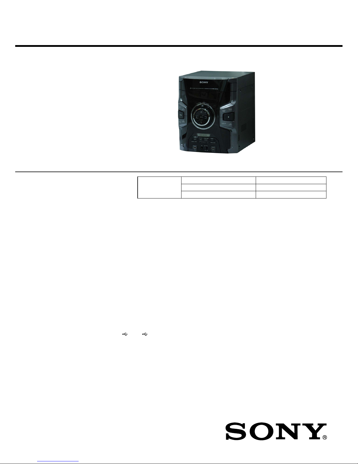
section in MHC-GPX8. Photo: HCD-GPX8G (E2 Model)
“WALKMAN” and “WALKMAN” logo are registered
trademarks of Sony Corporation.
MPEG Layer-3 audio coding technology and patents licensed
from Fraunhofer IIS and Thomson.
Windows Media is either a registered trademark or trademark
of Microsoft Corporation in the United States and/or other
countries.
This product contains technology subject to certain
intellectual property rights of Microsoft.
Use or distribution of this technology outside of this product
is prohibited without the appropriate license(s) from
Microsoft.
CD Section
Model Name Using Similar Mechanism
NEW
CD Mechanism Type
CDM74I-DVBU201//M
Optical Pick-up Name CMS-ST6RFS3
COMPACT DISC RECEIVER
Amplifi er section
The following are measured at Mexican model:
AC 120 V – 240 V, 60 Hz
Other models:
AC 120 V – 240 V, 50/60 Hz
MHC-GPX8
Front/Satellite speaker
Power Output (rated):
300 W + 300 W (at 4 ohms, 1 kHz,
1% THD)
Front speaker
RMS output power (reference):
360 W + 360 W (per channel at 6 ohms,
1 kHz)
Satellite speaker
RMS output power (reference):
180 W+ 180 W (per channel at 12 ohms,
1 kHz)
Subwoofer
RMS output power (reference):
260 W + 260 W (per channel at 8 ohms,
100 Hz)
MHC-GPX7
HIGH speakers
Power Output (rated):
300 W + 300 W (at 4 ohms, 1 kHz,
1% THD)
RMS output power (reference):
495 W + 495 W (per channel at 4 ohms,
1 kHz)
LOW speakers
RMS output power (reference):
180 W + 180 W (10 ohms, 100 Hz)
MHC-GPX5
Front speaker
Power Output (rated):
240 W + 240 W (at 5 ohms, 1 kHz,
1% THD)
RMS output power (reference):
370 W + 370 W (per channel at 5 ohms,
1 kHz)
Subwoofer
RMS output power (reference):
360 W (5 ohms, 100 Hz)
Inputs
TV (AUDIO IN) L/R
Voltage 1.2 V, impedance 47 kilohms
DVD/SAT (AUDIO IN) L/R
Voltage 1.2 V, impedance 47 kilohms
PC/GAME (AUDIO IN) L/R
Voltage 1.2 V, impedance 47 kilohms
MIC (MHC-GPX8/MHC-GPX7 only)
Sensitivity 1 mV, impedance
10 kilohms
A (USB), B (USB) port: Type A
USB section
Supported bit rate
MP3 (MPEG 1 Audio Layer-3):
32 kbps – 320 kbps, VBR
WMA: 48 kbps – 192 kbps
AAC: 48 kbps – 320 kbps
Sampling frequencies
MP3 (MPEG 1 Audio Layer-3):
32 kHz/44.1 kHz/48 kHz
WMA: 44.1 kHz
AAC: 44.1 kHz
Supported USB device
Mass Storage Class
Maximum current
500 mA
Disc player section
System
Compact disc and digital audio system
Laser Diode Properties
Emission Duration: Continuous
Laser Output*: Less than 44.6 μW
* This output is the value measurement
at a distance of 200 mm from the
objective lens surface on the Optical
Pick-up Block with 7 mm aperture.
Frequency response
20 Hz – 20 kHz
Signal-to-noise ratio
More than 90 dB
Dynamic range
More than 88 dB
Tuner section
FM stereo, FM/AM superheterodyne tuner
Antenna:
FM lead antenna
AM loop antenna
FM tuner section
Tuning range
87.5 MHz – 108.0 MHz (50 kHz step)
AM tuner section
Tuning range
Pan American models:
530 kHz – 1,710 kHz (10 kHz step)
531 kHz – 1,710 kHz (9 kHz step)
Other models:
530 kHz – 1,610 kHz (10 kHz step)
531 kHz – 1,602 kHz (9 kHz step)
General
Power requirements
Mexican model: AC 120 V – 240 V, 60 Hz
Other models: AC 120 V – 240 V, 50/60 Hz
Power consumption
MHC-GPX8: 250 W
MHC-GPX7: 230 W
MHC-GPX5: 200 W
Dimensions (w/h/d) (excl. speakers)
(Approx.)
280 mm × 355 mm × 440 mm
Mass (excl. speakers) (Approx.)
HCD-GPX8G/HCD-GPX7G/
HCD-GPX5G: 7.0 kg
Supplied accessories
Remote control (1)
R6 (Size AA) batteries (2)
FM lead/AM loop antenna (1)
Spacer A (MHC-GPX8 only) (2)
Spacer B (MHC-GPX8 only) (2)
Speaker pads (MHC-GPX7 only) (8)
Design and specifi cations are subject to change
without notice.
HCD-GPX5G/GPX7G/GPX8G
2
NOTES ON CHIP COMPONENT REPLACEMENT
• Never reuse a disconnected chip component.
• Notice that the minus side of a tantalum capacitor may be
damaged by heat.
FLEXIBLE CIRCUIT BOARD REPAIRING
• Keep the temperature of soldering iron around 270 °C during
repairing.
• Do not touch the soldering iron on the same conductor of the
circuit board (within 3 times).
• Be careful not to apply force on the conductor when soldering
or unsoldering.
SAFETY-RELATED COMPONENT WARNING!
COMPONENTS IDENTIFIED BY MARK 0 OR DOTTED LINE
WITH MARK 0 ON THE SCHEMATIC DIAGRAMS AND IN
THE PARTS LIST ARE CRITICAL TO SAFE OPERATION.
REPLACE THESE COMPONENTS WITH SONY PARTS
WHOSE PART NUMBERS APPEAR AS SHOWN IN THIS
MANUAL OR IN SUPPLEMENTS PUBLISHED BY SONY.
CAUTION
Use of controls or adjustments or performance of procedures
other than those specifi ed herein may result in hazardous
radiation exposure.
SAFETY CHECK-OUT
After correcting the original service problem, perform the following
safety check before releasing the set to the customer:
Check the antenna terminals, metal trim, “metallized” knobs,
screws, and all other exposed metal parts for AC leakage.
Check leakage as described below.
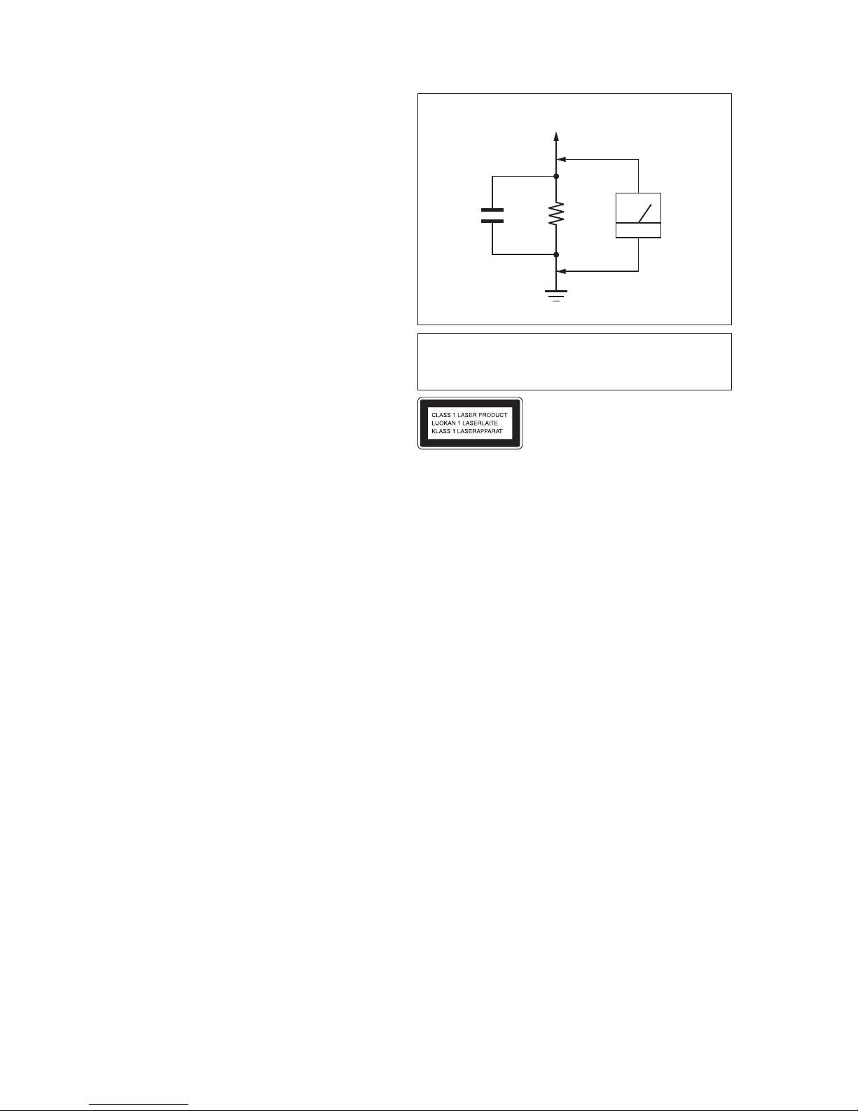
LEAKAGE TEST
The AC leakage from any exposed metal part to earth ground and
from all exposed metal parts to any exposed metal part having a
return to chassis, must not exceed 0.5 mA (500 microamperes.).
Leakage current can be measured by any one of three methods.
1. A commercial leakage tester, such as the Simpson 229 or RCA
WT-540A. Follow the manufacturers’ instructions to use these
instruments.
2. A battery-operated AC milliammeter. The Data Precision 245
digital multimeter is suitable for this job.
3. Measuring the voltage drop across a resistor by means of a
VOM or battery-operated AC voltmeter. The “limit” indication
is 0.75 V, so analog meters must have an accurate low-voltage
scale. The Simpson 250 and Sanwa SH-63Trd are examples
of a passive VOM that is suitable. Nearly all battery operated
digital multimeters that have a 2 V AC range are suitable. (See
Fig. A)
1.5 kΩ0.15 μF
AC
voltmeter
(0.75 V)
To Exposed Metal
Parts on Set
Earth Ground
Fig. A. Using an AC voltmeter to check AC leakage.
This appliance is classified as a CLASS 1
LASER product. This marking is located on
the rear exterior.

HCD-GPX5G/GPX7G/GPX8G
3
TABLE OF CONTENTS
1. SERVICING NOTES
................................................ 4
2. DISASSEMBLY
2-1. Disassembly Flow ........................................................... 8
2-2. Case ................................................................................. 9
2-3. Loading Panel ................................................................. 9
2-4. Front Panel Section ......................................................... 10
2-5. CD Mechanism Section (CDM741-DVBU201//M) ....... 10
2-6. TUNER1AM3R Board ................................................... 11
2-7. MAIN Board ................................................................... 11
2-8. Back Panel Section ......................................................... 12
2-9. 4CH DAMP board .......................................................... 13
2-10. Chassis Section ............................................................... 14
2-11. Cover Dust CDM ........................................................... 15
2-12. Optical Pick Up ............................................................... 15
2-13. DMB22 Board ................................................................. 16
2-14. DRIVER Board, SWITCH Board ................................... 16
2-15. SENSOR Board .............................................................. 17
2-16. MOTOR (TB) Board....................................................... 17
2-17. MOTOR (LD) Board ...................................................... 18
3. TEST MODE ............................................................. 19
4. ELECTRICAL CHECK .......................................... 22
5. DIAGRAMS
5-1. Block Diagram - CD/USB Section - ............................... 23
5-2. Block Diagram - MAIN Section - ................................... 24
5-3. Block Diagram - AMP Section - ..................................... 25
5-4. Block Diagram - PANEL/POWER SUPPLY Section - .. 26
5-5. Printed Wiring Board -
4CH DAMP Board (Component side) ............................ 28
5-6. Printed Wiring Board -
4CH DAMP Board (Conductor side) .............................. 29
5-7. Schematic Diagram - 4CH DAMP Board (1/3) - ............ 30
5-8. Schematic Diagram - 4CH DAMP Board (2/3) - ............ 31
5-9. Schematic Diagram - 4CH DAMP Board (3/3) - ............ 32
5-10. Printed Wiring Board - DISPLAY Board - ..................... 33
5-11. Schematic Diagram - DISPLAY Board - ........................ 34
5-12. Printed Wiring Board -
MAIN Board (Component side) ..................................... 35
5-13. Printed Wiring Board -
MAIN Board (Conductor side) ....................................... 36
5-14. Schematic Diagram - MAIN Board (1/4) - ..................... 37
5-15. Schematic Diagram - MAIN Board (2/4) - ..................... 38
5-16. Schematic Diagram - MAIN Board (3/4) - ..................... 39
5-17. Schematic Diagram - MAIN Board (4/4) - ..................... 40
5-18. Printed Wiring Board -
USB, VOLUME and MIC Board - ................................. 41
5-19. Schematic Diagram -
USB, VOLUME and MIC Board - ................................. 42
5-20. Printed Wiring Board - DRIVER, SENSOR, SWITCH,
MOTOR (LD) and MOTOR (TB) Board ....................... 43
5-21. Schematic Diagram - DRIVER, SENSOR, SWITCH,
MOTOR (LD) and MOTOR (TB) Board - ..................... 44
5-22. Printed Wiring Board - TUNER1AM3R Board ............. 45
5-23. Schematic Diagram - TUNER1AM3R Board - .............. 45
5-24. Printed Wiring Board - DMB22 Board - ........................ 46
5-25. Schematic Diagram - DMB22 Board (1/3) - .................. 47
5-26. Schematic Diagram - DMB22 Board (2/3) - .................. 48
5-27. Schematic Diagram - DMB22 Board (3/3) - .................. 49
6. EXPLODED VIEWS
6-1. Case Section ................................................................... 61
6-2. Front Panel Section ........................................................ 62
6-3. Back Panel Section ......................................................... 63
6-4. Chassis Section ............................................................... 64
6-5. CD Mechanism Section (1)
(CDM74I-DVBU201//M) ............................................... 65
6-6. CD Mechanism Section (2) ............................................. 66
7. ELECTRICAL PARTS LIST ............................... 67
HCD-GPX5G/GPX7G/GPX8G
4
SECTION 1
SERVICING NOTES
NOTES ON HANDLING THE OPTICAL PICK-UP
BLOCK OR BASE UNIT
The laser diode in the optical pick-up block may suffer electrostatic break-down because of the potential difference generated by
the charged electrostatic load, etc. on clothing and the human body.
During repair, pay attention to electrostatic break-down and also
use the procedure in the printed matter which is included in the
repair parts.
The fl exible board is easily damaged and should be handled with
care.
UNLEADED SOLDER
Boards requiring use of unleaded solder are printed with the leadfree mark (LF) indicating the solder contains no lead.
(Caution: Some printed circuit boards may not come printed with
the lead free mark due to their particular size)
: LEAD FREE MARK
Unleaded solder has the following characteristics.
• Unleaded solder melts at a temperature about 40 °C higher
than ordinary solder.
Ordinary soldering irons can be used but the iron tip has to be
applied to the solder joint for a slightly longer time.
Soldering irons using a temperature regulator should be set to
about 350 °C.
Caution: The printed pattern (copper foil) may peel away if
the heated tip is applied for too long, so be careful!
• Strong viscosity
Unleaded solder is more viscous (sticky, less prone to fl ow)
than ordinary solder so use caution not to let solder bridges
occur such as on IC pins, etc.
• Usable with ordinary solder
It is best to use only unleaded solder but unleaded solder may
also be added to ordinary solder.
NOTE OF REPLACING THE IC502 ON THE DMB22
BOARD
IC502 on the DMB22 board cannot exchange with single.
When these parts on the DMB22 board are damaged,
exchange the entire mounted board.
RELEASING THE DISC TRAY LOCK
The disc tray lock function for the antitheft of an demonstration
disc in the store is equipped.
Releasing Procedure:
1. Press [I/
1
STANDBY] button to turn the power on.
2. Press the [CD/DISC SKIP] button to select CD function.
3. While pressing the [x] button, press the [ENTER] button for
more 5 seconds).
4. The message “UNLOCKED” is displayed and the disc tray is
unlocked.
Note: When “LOCKED” is displayed, the slot lock is not released by
turning power on/off with the
[I/1 STANDBY] button.
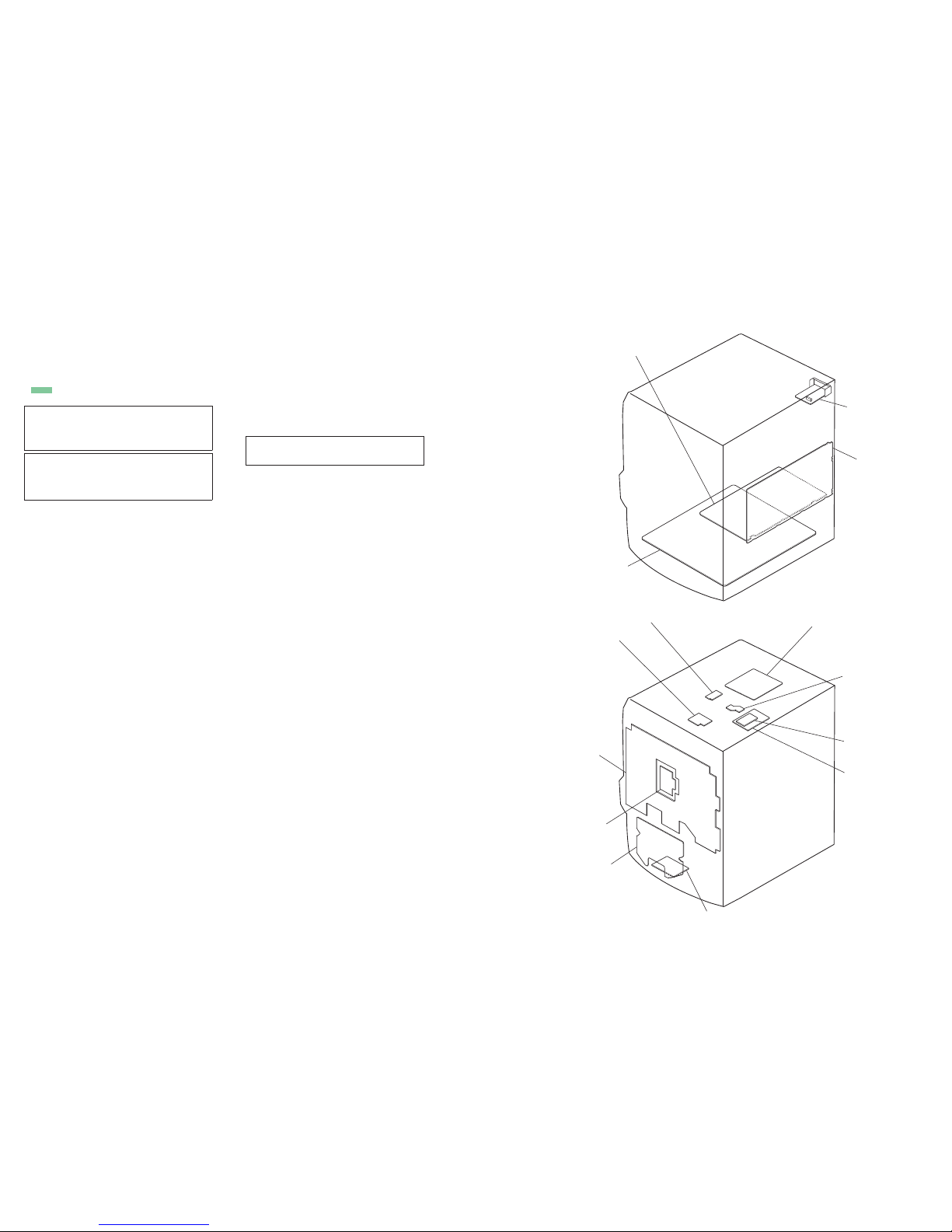
MODEL IDENTIFICATION
– Back Panel –
Model Part No.
HCD-GPX8G: E2, E51, E4
4-411-595-0[]
HCD-GPX7G: E2, E51
4-411-595-1[]
HCD-GPX5G: E2, E51
4-411-595-2[]
HCD-GPX8G: MX
4-411-595-3[]
HCD-GPX7G: MX
4-411-595-4[]
HCD-GPX5G: MX
4-411-595-5[]
NOTES ON LASER DIODE EMISSION CHECK
The laser beam on this model is concentrated so as to be focused
on the disc refl ective surface by the objective lens in the optical
pickup block. Therefore, when checking the laser diode emission,
observe from more than 30 cm away from the objective lens.
PART No.
Note : Refer to SUPPLEMENT-1 for adding SERVICING
NOTES (TROUBLESHOOTING)
Ver. 1.1
HCD-GPX5G/GPX7G/GPX8G
5
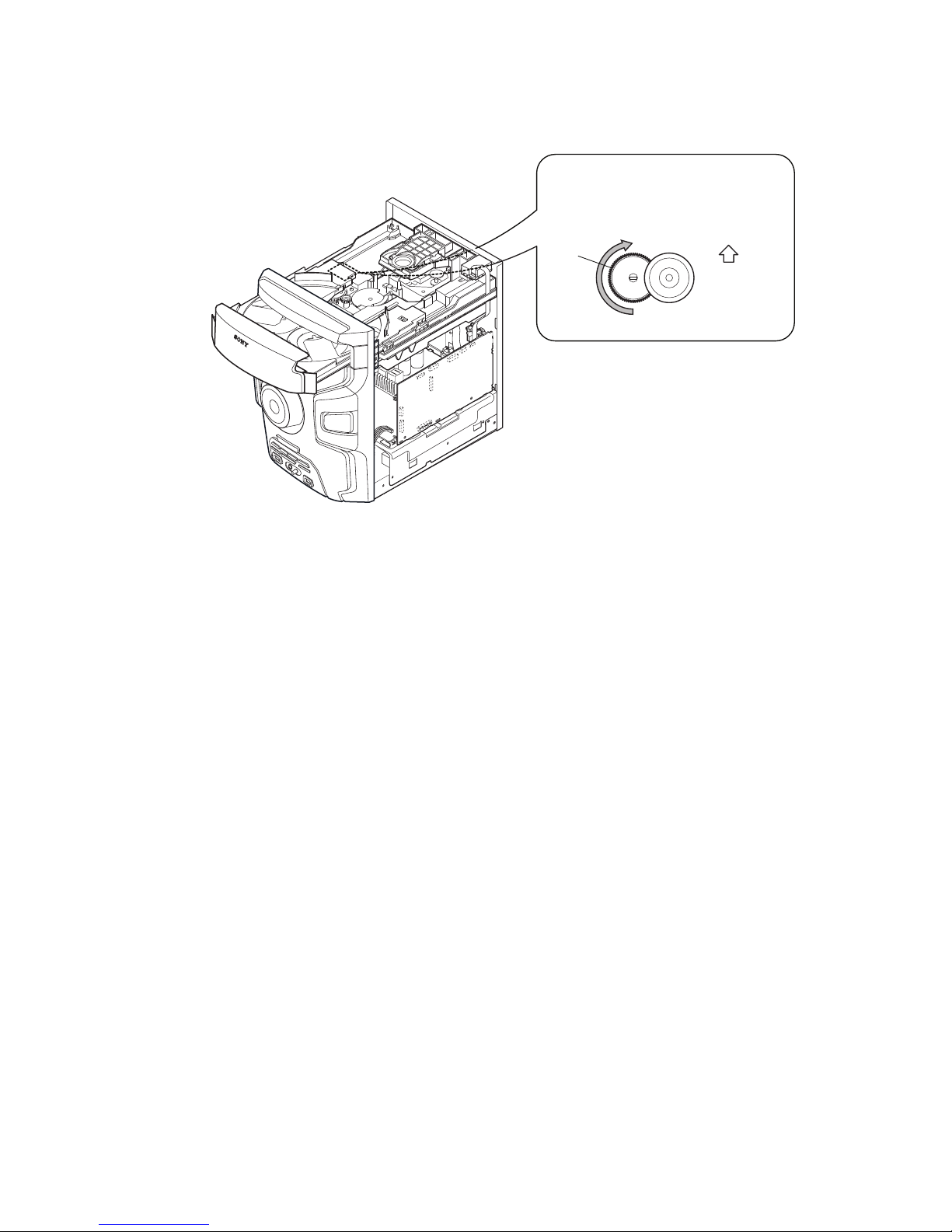
HOW TO OPEN THE TRAY WHEN POWER SWITCH TURN OFF
gear
chassis side
CD mechanism deck (CDM74I)
By using (-) screw driver
1 Turn the gear to the direction of the arrow.
(The location of this gear pulley is at the
bottom side of the CDM)
HCD-GPX5G/GPX7G/GPX8G
6
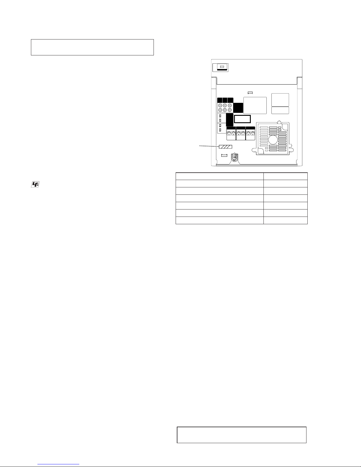
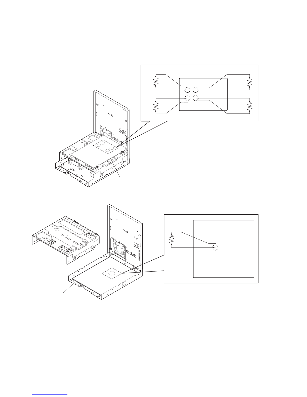
CAPACITOR DISCHARGE FOR ELECTRIC SHOCK PREVENTION
:
&
&
&
C1431
&
:
:
:
4CH DAMP board
in checking the DAMP 4CH board, make a capacitor
GLVFKDUJHRI&RU&RU&DQG&
for electrical shock prevention.
LQFKHFNLQJWKH5(*8/$7256:,7&+,1*ERDUGPDNH
DFDSDFLWRUGLVFKDUJHRI&IRUHOHFWULFDOVKRFNSUHYHQWLRQ
5(*8/$7256:,7&+,1* board
:
HCD-GPX5G/GPX7G/GPX8G
7
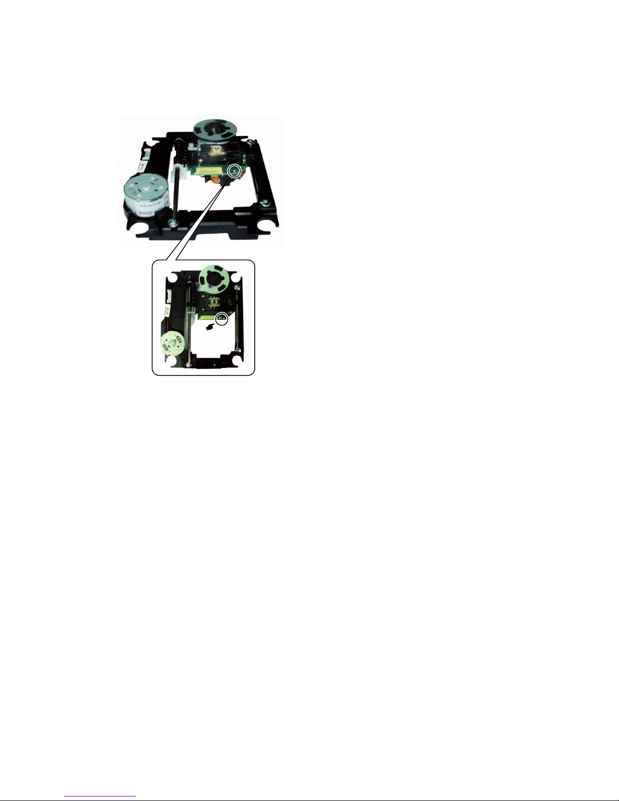
PRECAUTION WHEN INSTALLING A NEW OP UNIT/
PRECAUTION BEFORE UNSOLDERING THE STATIC
ELECTRICITY PREVENTION SOLDER BRIDGE
When installing a new OP unit, be sure to connect the fl exible
printed circuit board fi rst of all before removing the static electric-
ity prevention solder bridge by unsoldering.
Remove the static electricity prevention solder bridge by unsoldering after the fl exible printed circuit board has already been con-
nected.
(Do not remove nor unsolder the solder bridge as long as the OP
unit is kept standalone.)
HCD-GPX5G/GPX7G/GPX8G
8
SECTION 2
DISASSEMBLY
• This set can be disassembled in the order shown below.
2-1. DISASSEMBLY FLOW
2-2. CASE
(Page 9)
2-5. CD MECHANISM SECTION
(CDM74I-DVBU201/M)
(Page 10)
2-7. MAIN BOARD
(Page 11)
2-8. BACK PANEL SECTION
(Page 12)
2-9. 4CH DAMP BOARD
(Page 13)
2-10. CHASSIS SECTION
(Page 14)
2-11. COVER DUST CDM
(Page 15)
2-13. DMB22 BOARD
(Page 16)
2-12. OPTICAL PICK UP
(Page 15)
2-15. SENSOR BOARD
(Page 17)
2-14. DRIVER BOARD, SWITCH BOARD
(Page 16)
2-16. MOTOR (TB) BOARD
(Page 17)
2-17. MOTOR (LD) BOARD
(Page 18)
2-6. TUNER1AM3R BOARD
(Page 11)
2-4. FRONT PANEL SECTION
(Page 10)
SET
2-3. LOADING PANEL
(Page 9)
HCD-GPX5G/GPX7G/GPX8G
9
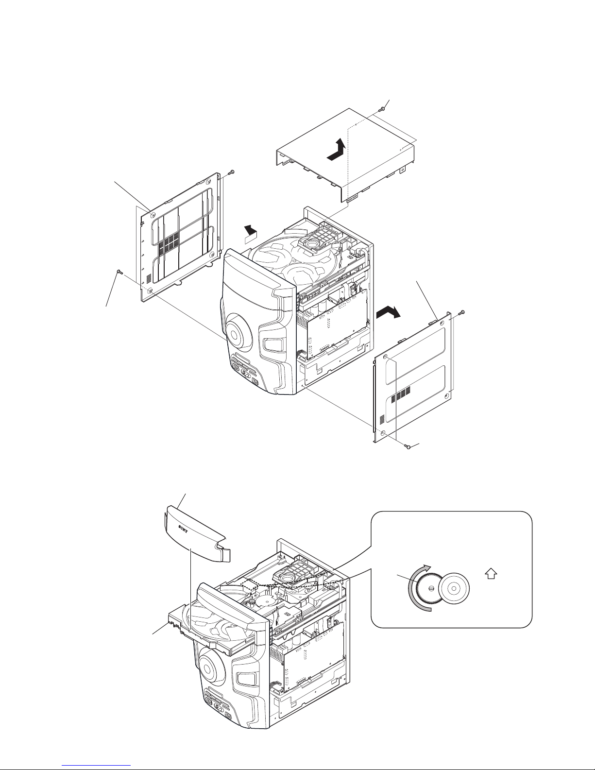
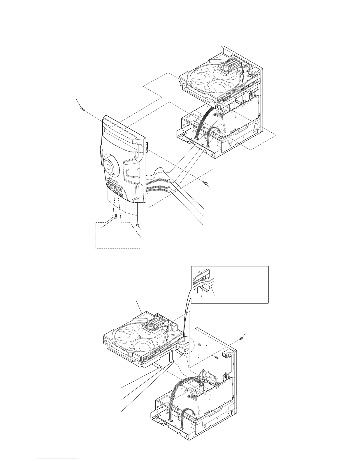
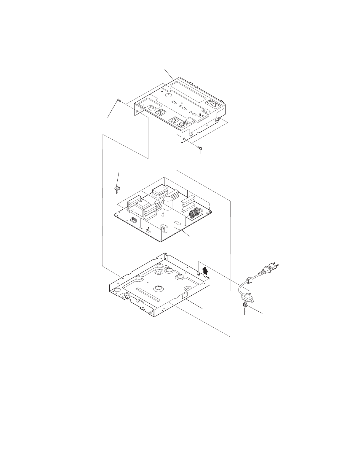
2-3. LOADING PANEL
Note: Follow the disassembly procedure in the numerical order given.
2-2. CASE
56 two screws
(+BVTP 3x14)
two screws
(+BVTP 3x14)
1
2 two screws
(+BVTP 3x14)
(+BVTP 3x14)
2
3
3
two screws
1 two screws
(+BVTP 3x14)
4 panel, side (R)
4 panel, side (L)
2 Pull-out the disc tray
3
panel, loading
gear
chassis side
CD mechanism deck (CDM74I)
By using (-) screw driver
1 Turn the gear to the direction of the arrow.
(The location of this gear pulley is at the
bottom side of the CDM)
HCD-GPX5G/GPX7G/GPX8G
10
2-5. CD MECHANISM SECTION (CDM74I-DVBU201//M)
2-4. FRONT PANEL SECTION
1 four screws
(+BVTP 3x8)
1
one screws
(+BVTP 3x8)
For GPX7G/
GPX8G
2 one screw
(+BVTP 3x8)
2 one screw
(+BVTP 3x8)
5
CN705 (10P)
4
CN707 (4P)
3
wire (flat type) (17core) CN601
CD mechanism section
( CDM74I-DVBU201//M)
Peel off the cushion
and tape on the wire
(flat type) from TUNER.
4 one screw
(BVTP 3x8)
2
wire (flat type) (19core) CN702
3
wire (flat type) (15core) CN703
1
wire (flat type) (13core) CN700
tape
cushion
HCD-GPX5G/GPX7G/GPX8G
11
2-6. TUNER1AM3R BOARD
2-7. MAIN BOARD
2
5
3
4
two screws
(BVTP 3x8)
1 wire (flat type) (9 core)
(CN513)
TUNER1AM3R board
shield plate bottom
shield plate top
1 two screws
(+BVTP 3x8)
2 two screws
(+BVTP 3x8)
3 MAIN board
HCD-GPX5G/GPX7G/GPX8G
12
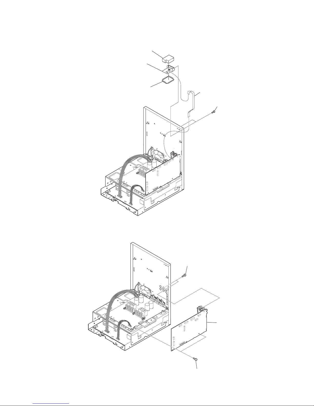
2-8. BACK PANEL SECTION
6 two screws
(BVTP 3x8)
7
8 one screws
(BVTP 3x8)
2 two screws
(BVTP 3x8)
3 two screws
(BVTP 3x8)
one screw
(+BVTP 3x8)
for GPX8G
1 CN1405 (3P)
5 fan, DC
4 cover, fan
9 back panel section
HCD-GPX5G/GPX7G/GPX8G
13
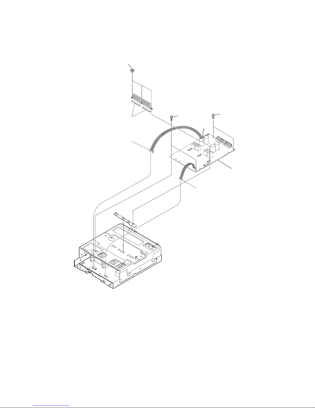
2-9. 4CH DAMP BOARD
3 two screws
(BVTT 3x8)
1 three screws
(PTPWH 2.6x12)
6 4CH DAMP board
42 CN2 (9P)
5 CN3 (5P)
sheet thermal
3 two screws
(BVTT 3x8)
HCD-GPX5G/GPX7G/GPX8G
14
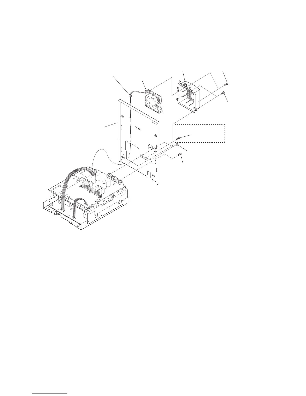
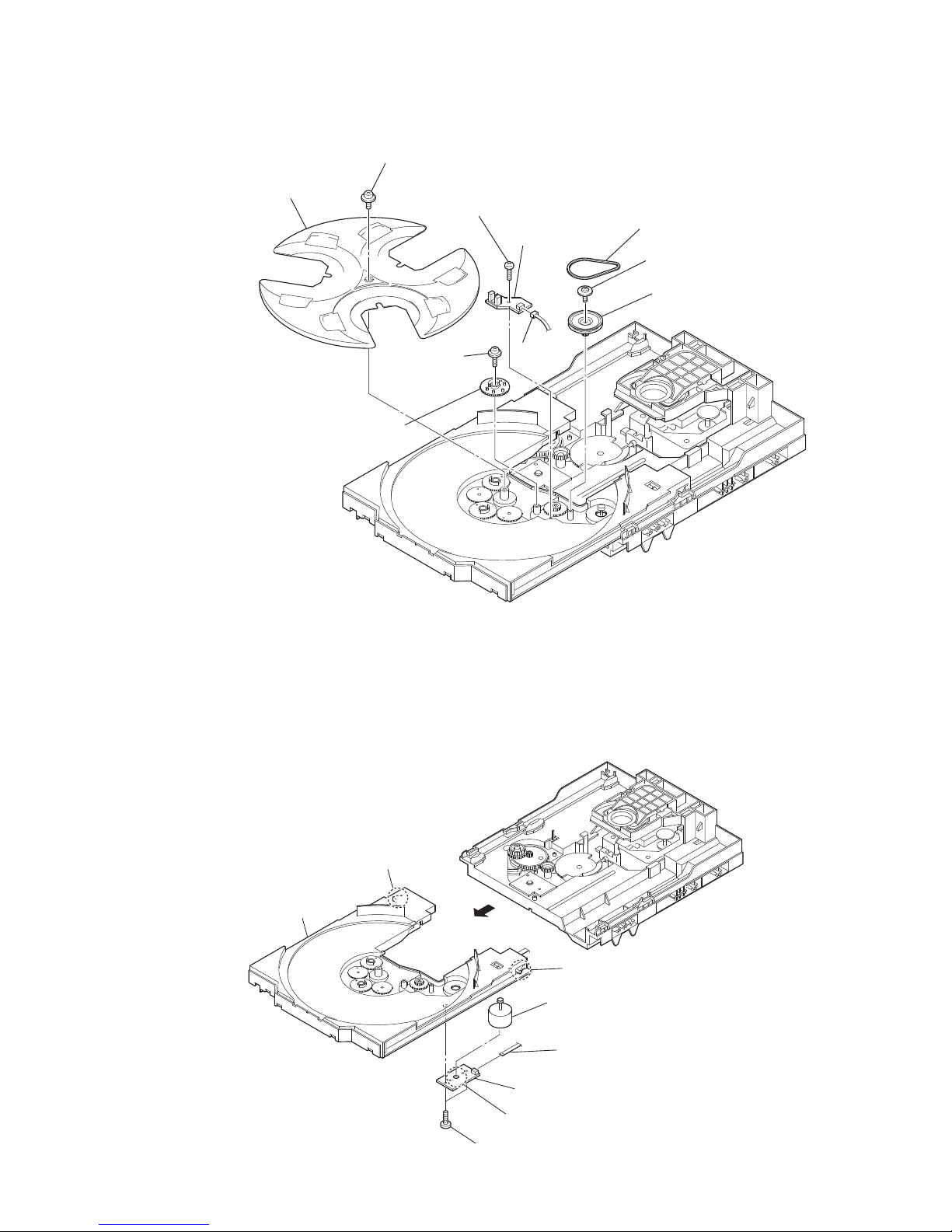
2-10. CHASSIS SECTION
6
REGULATOR,
SWITCHING
5 nine screws
(+PWH 3x8)
1 two screws
(+BVTP 3x8)
two screws
(+BVTP 3x8)
1
2 bracket, SMPS (shield)
4
7 chassis
3 CN1 (2P)
E
HCD-GPX5G/GPX7G/GPX8G
15
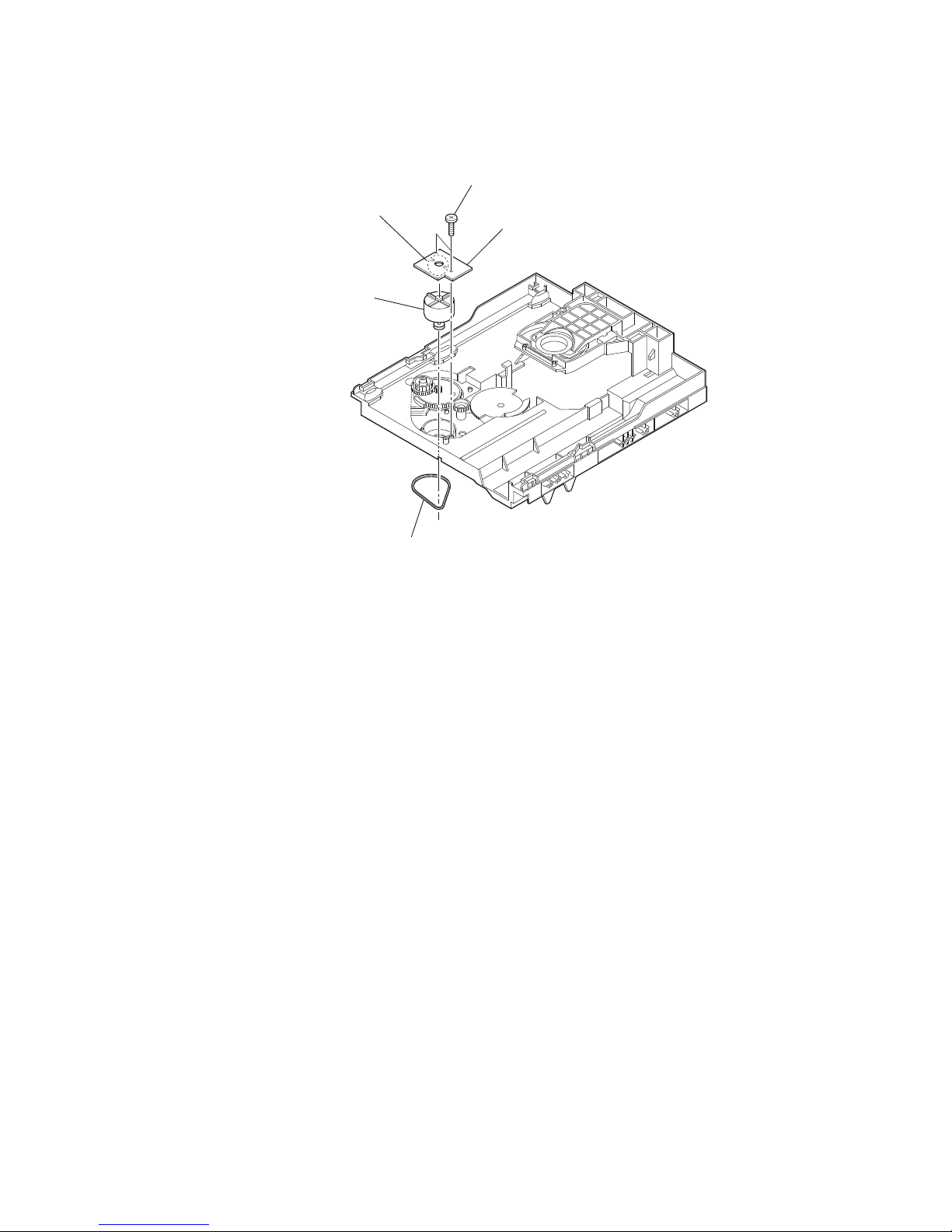
2-11. COVER DUST CDM
3 four screws
(+BVTP 3x10)
1 two screws
1 two screws
5 go through the
hole of cover dust
6 CDM74I
2 cover dust (CDM)
4 bracket, holder (DMB)
(+BVTP 3x10)
(+BVTP 3x10)
2-12. OPTICAL PICK UP
3 insulator screw
3 insulator screw
3 insulator screw
3 insulator screw
4 insulator
4 insulator
4 insulator
4 insulator
6
device, optical
(CMS-ST6RFS3)
5
solder the short land
1 floating screw
(
+PTPWH M2.6)
2 CDM74I assy
Solder the short-land
(Location of this point is at the bottom
side of optical device)
HCD-GPX5G/GPX7G/GPX8G
16
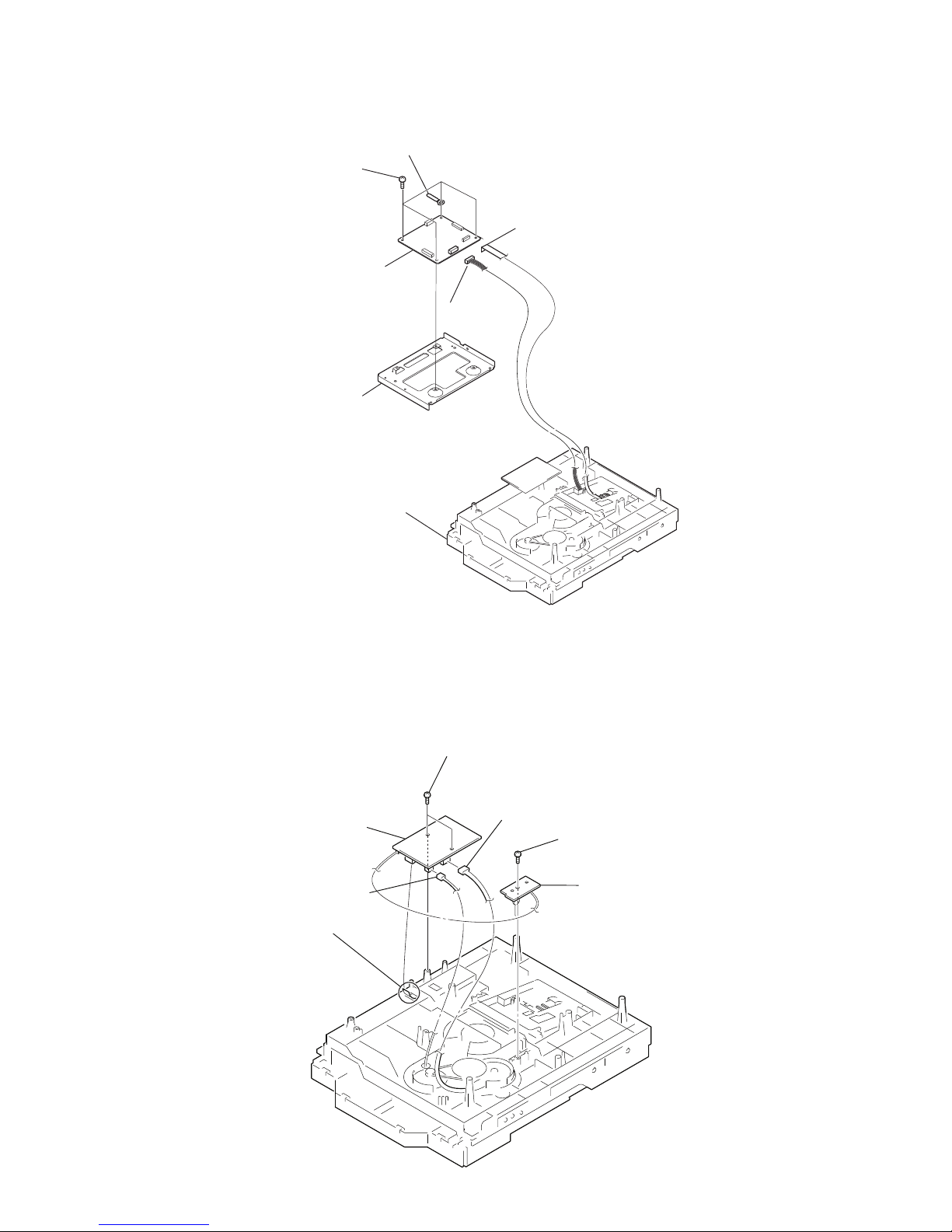
2-14. DRIVER BOARD, SWITCH BOARD
1 two screws
(+BTTP (M2.6))
6 one screw
(+BTTP (M2.6))
7 SWITCH board
2 CN703 (4P)
3 CN704 (2P)
4 wire (flat type) (5 core)
(CN702)
5 DRIVER board
2-13. DMB22 BOARD
7 CDM74I-DVBU201//M
5
DMB22 board
2 clamp
3 CN801 (6P)
6 bracket, holder (DMB)
1 four screws
(+BVTP 3x10)
4 wire (flat type)
(21core) (CN501)
HCD-GPX5G/GPX7G/GPX8G
17
2-15. SENSOR BOARD
3 wire (flat type) (5 core)
(CN742)
4 two screws
(+BTTP (M2.6))
5 motor assy, table (M741)
6 remove the two solderings of motor
7 MOTOR (TB) board
1 gear (stopper)
1 gear (stopper)
2
table
2-16. MOTOR (TB) BOARD
1 floating screw
(+PTPWH M2.6)
4 floating screw
(+PTPWH M2.6)
8 one screw
(+BTTP (M2.6))
6 floating screw
(+PTPWH M2.6)
7 gear (geneva)
2 tray
3 belt (table)
9 CN731
(3P)
0 SENSOR board
5 pulley (table)
HCD-GPX5G/GPX7G/GPX8G
18
2-17. MOTOR (LD) BOARD
1 belt (loading)
2 remove the two solderings of motor
4 motor assy, loading (M751)
5 MOTOR (LD) board
3 two screws
(+BTTP (M2.6))

HCD-GPX5G/GPX7G/GPX8G
19
SECTION 3
TEST MODE
[PANEL TEST MODE]
• This mode is used to check the fl uorescent indicator tube,
LEDs, keys, [MASTER VOLUME] jog, model, destination and software version.
• Procedure:
1. Press [CD/DISC SKIP] button and [TUNER/BAND]
button simultaneously and hold 3 seconds.
2. All LEDs and segments in fl uorescent indicator tube are
lighted up.
3. When you want to enter to the software version display
mode, press [
+
/ ] button.
The model information
appears on the fl uorescent indicator tube.
• “GPX 3S” is shown for MHC-GPX5.
• “GPX 4” is shown for MHC-GPX7.
• “GPX 7S” is shown for MHC-GPX8.
Press [
+
/ ] button again to view the destination
information.
4. During the destination information display, press [
+
/ ] button. Each time [
+
/ ] button is pressed, the
fl
uorescent indicator tube shows the version of each category
software in the following sequence: SC, MTK (DMB Board
fi rmware version), UI, PF, SYS, CD, CDMA, CDMB,
ST, TA, TAS, TM and return back to model information
display.
5. When [OPTION] button is pressed while the version
numbers are being displayed except model and destination,
the date of the software creation appears. When [OPTION]
button is pressed again, the display returns to the software
version display.
6. Press [
+
/ ↓] button, the key check mode is activated.
7. In the key check mode, the fl uorescent indicator tube
displays “K 0 V0”.
Each time a button is pressed, “K” value increases.
However, once a button has been pressed, it is no longer
taken into account.
“V” value increases in the manner of 0,1, 2, 3 ... if [MAS-
TER VOLUME] knob is turned clockwise, or it decreases
in the manner of 0, 9, 8,7 ... if [MASTER VOLUME] knob
is turned counterclockwise.
8. When [ENTER] button is pressed after all LEDs and
segments in fl uorescent indicator tube light up, alternate
segments in fl uorescent indicator tube and LEDs would
light up. If you press [ENTER] button again, another half
of alternate segments in fl uorescent indicator tube and
LEDs would light up. Pressing [ENTER] button again
would cause all segments in fl uorescent indicator tube and
LEDs light up.
9. To release from this mode, press three buttons in the same
manner as step 1, or disconnect the power cord.
[COMMON TEST MODE]
• This mode is used to check operations of the Amplifi er
section.
• Procedure:
• To enter Common Test Mode
1. Press [USB/USB SELECT] button and [BASS BAZUCA]
button simultaneously and hold for 3 seconds.
2. The function is changed to TV and the volume is changed
to VOLUME MIN.
• Check of Amplifi er
1. Press [MUSIC] button repeatedly until a message “GEQ
MAX” appears on the fl uorescent indicator tube. GEQ in-
creases to its maximum.
2. Press [MUSIC] button repeatedly until a message “GEQ
MIN” appears on the fl uorescent indicator tube. GEQ
decreases to its minimum.
3. Press [MUSIC] button repeatedly until a message “GEQ
FLAT” appears on the fl uorescent indicator tube. GEQ is
set to fl at.
4. When the [MASTER VOLUME] knob is turned clockwise
even slightly, the sound volume increases to its maximum
and a message “VOLUME MAX” appears on the fl uores-
cent indicator tube.
5. When the [MASTER VOLUME] knob is turned counterclockwise even slightly, the sound volume decreases to its
minimum and a message “VOLUME MIN” appears on the
fl uorescent indicator tube.
• To release from Common Test mode
1. To release from this mode, press [
I/1 STANDBY] button.
2. The cold reset is enforced at the same time.
[USER RESET]
• The user reset clears all data including preset data stored
in the data fl ash to initial conditions exclude history mode
data
• Procedure:
1. Press [
I/1 STANDBY] button to turn on the system.
2.
Press [x] button and [
I/1 STANDBY
] button simultane
ously for 3 seconds.
3.“RESET” appears on the fl uorescent indicator tube.
After that, the fl uorescent indicator tube becomes blank
for a while, and the system is reset.
[COLD RESET]
• The cold reset clears all data including preset data stored in
the data fl ash to initial conditions. Execute this mode when
returning the set to the customer.
• Procedure:
1. Press [
I/1 STANDBY] button to turn on the system.
2. Press [ENTER] button and [GAME] button
simultaneously for 3 seconds.
3. “COLD RESET” appears on the fl uorescent
indicator tube. After that, the fl uorescent indicator
tube becomes blank for a while, and the system is
reset.
[TUNER STEP CHANGE]
• The step interval of AM channels can be toggled between
9 kHz and 10 kHz. This mode is not available for Saudi
Arabian, European and Russian models.
• Procedure:
1. Press [
I/1 STANDBY] button to turn on the system.
2. Press [TUNER/BAND] button repeatedly to select
the “AM”.
3. Press [
I/1 STANDBY] button to turn off the system.
4. Press [LED EFFECT] button and [
I/1 STANDBY]
button simultaneously. The system turns on
automatically. The message “AM 9K STEP”
or “AM 10K STEP” appears on the fl uorescent
indicator tube and thus the channel step is changed.
[CD SHIP MODE (WITH MEMORY CLEAR)]
• This mode moves the optical pick-up to the position
durable to vibration and clears all data including preset
data stored in the EEPROM to initial conditions during the
next AC-In. Use this mode when returning the set to the
customer after repair.
• Procedure:
1. Press [
I/1 STANDBY] button to turn on the system.
2. Select CD function.
3. Press [ENTER] button and [MUSIC] button
simultaneously for 3 seconds. The system turns off
automatically.
4. A message
“MECHA LOCK” is displayed on the fl uorescent
indicator tube and the CD ship mode is set.
HCD-GPX5G/GPX7G/GPX8G
20
[CD SHIP MODE (WITHOUT MEMORY CLEAR)]
• This mode moves the optical pick-up to the position durable to vibration. Use this mode when returning the set to
the customer after repair.
• Procedure:
1. Press [
I/1 STANDBY] button to turn on the system.
2. Select CD function.
3. Press [BASS BAZUCA] button and [
I/1 STANDBY]
button simultaneously. The system turns off
automatically.
4. A message
“MECHA LOCK” is displayed on the fl uorescent
indicator tube and the CD ship mode is set.
[CD TRAY LOCK MODE]
• This mode let you lock the disc tray. When this mode is activated, the disc tray will not open when [
Z
OPEN/CLOSE]
button or [EX-CHANGE] button is pressed. The message
“LOCKED” will be displayed on the fl uorescent indicator
tube. This mode only applied when there is disc(s) on the
tray.
• Procedure:
1. Press [
I/1 STANDBY] button to turn on the system.
2. Select CD function.
3. Press [
x
] button and [ENTER] button simultaneously and hold down until “LOCKED” or “UNLOCKED” displayed on the fl uorescent indicator
tube (around 5 seconds).
[FACTORY PRESET]
• This mode is use to load all the factory use preset frequencies into FM 1-FM 20 and AM 1-AM 10. Originally, frequency of FM 1-FM 20 and AM 1-AM10 are set to the
minimum frequency.
• Procedure:
1. Press [
I/1 STANDBY] button to turn on the system.
2. Press [CD/DISC SKIP] button and [AUDIO IN]
button simultaneously and hold for 3 seconds,
message “FACTORY” appears on the fl uorescent
indicator tube. The function is changed to TUNER
automatically.
[CDM AGING MODE]
• This mode is used to display the total count of meter
pointer touch initial switch and max switch.
• Procedure:
1. Press [
I/1 STANDBY] button to turn on the system.
2. Select CD function and All DISC play mode.
3. Put discs on all trays and close the tray.
4. Press [
+
/ ] button and [
x
] button simultane-
ously for 3 seconds.
5. The fl uorescent indicator tube displays Aging
Display “AG xxxx/yyyy”.
“xxxx” represents the error counter
(Maximum Value of “xxxx” = 9999)
“yyyyy” represents the cycle counter
(Maximum Value of “yyyy” = 9999)
6. Press [<<] or [>>] to search for Aging History
Error Display.
The fl uorescent indicator tube displays
“Mx E1E2E3E4”.
x: error history number
E1: Loading sequence JCP high
E2: Loading sequence JCP low
E3: Loading operation JCP
E4: Cam position operation JCP
7. Press [ENTER] to Aging Display
• To release from Meter Aging Mode.
To release from this mode, press [
I/1 STANDBY] button or
perform COLD RESET operation.
[HISTORY MODE]
• This mode is used to check important data stored in the
system when PROTECTOR happen.
• Procedure:
1. During demo mode, press [
u] button and [BASS
BAZUCA] for 5 seconds to mode in to history
mode.
2. Press the [TUNING +] or [TUNING -] button to
check history data stored
Item Display
Protector Count P R O C O U N T
Protector Type P R O T Y P E
Single Power On Time T 1 H M
Total Power On Time T 2
H M
Input Function F U N C
Volume V O L
Actual Attenuation A T T
Low EQ Level E Q L O W
Mid EQ Level E Q M I D
High EQ Level E Q H I G H
VACS Level V A C S
AP VACS Level A P V A C S
Subwoofer Setting S W
Surround Setting S U R R
DJ Effect Setting D J
Bass Bazuca Setting B A Z U C A
• To release from History Mode.
To release from this mode, press [
I/1 STANDBY] button.
[PROTECT KIND CHECK TEST MODE]
• This mode is used to check types of protect occurred during
protector on.
• Procedure:
3. During protection on, fl uorescent indicator tube
shows blinking message “PROTECT EXX”.
“EXX” – represent the error code.
4. Press [
u] button & [
x
] button simultaneously.
5. Fluorescent indicator tube display will toggle
between “PROTECT” message & protector kind
message display.
Bellow table explains on protector kind.
Error Code Protector Message Description
E01 "AMP OCP"
The over current condition to MOSFET occurs by defect of MOSFET or
defect of PS output line.
E02 "MTK POWER" No power supply to DMB mount
E03 "POWER SUPPLY" Defect of power supply circuit to AMP
E04 "AMPLIFIER" Defect of AMP circuit
E06 "FAN BLOCK"
Defect of DC FAN and DC FAN
driver circuit
• To release from this mode.
Press [
u] button & [
x
] button simultaneously again or
unplug & re-plug in the power cord.
HCD-GPX5G/GPX7G/GPX8G
21
1. Defect of AMP circuit
1-1. If PROTECT mode is “AMPLIFIER”,
The following defect might be possible.
Defects Possible cause
OTP (Over Tempera-
ture Protection)
Unusual heat up of MOSFET by improper assembly of heatsink, destruction
of MOSFET etc..
DC Detection
DC appears in SP terminal by defect of
AMP IC and MOSFET or output is shortcircuit.
Unusual output of
Power mount
The power mount has unusual output.
1-2. If speaker does not have output even if the set status is not
in PROTECT mode
The following defect might be possible.
Defects Possible cause
Under Voltage IC1402 output is below 12V.
RESET defect Reset signal status from micom is not ‘H’.
2. Defect of power supply circuit to AMP
2-1. If the PROTECT mode is “POWER SUPPLY”,
There is possibility of unusual power supply of any of the
AMP IC or Pre-amplifi er.
• To release from this mode.
Press [
u] button and [
x
] button simultaneously
again or unplug and re-plug in the power cord.
HCD-GPX5G/GPX7G/GPX8G
22
CD SECTION
Note:
1. CD Block is basically constructed to operate without adjustment.
2. Use YEDS-18 disc (Part No. 3-702-101-01) unless otherwise indicated.
3. Use an oscilloscope with more than 10 MΩ impedance.
4. Clean the object lens by an applicator with neutral detergent when the
signal level is low than specifi ed value with the following checks.
5. Check the focus bias check when optical pick-up block is replaced.
FOCUS BIAS CHECK
Procedure :
1. Connect the oscilloscope to CN507 pin 6 (RFMON) and
CN507 pin 3 (GND) on the DMB22 board.
2. Press the [
?/1
STANDBY] button to turn the power on, and
press the [CD/DISC SKIP] button to select CD function.
3. Set disc (YEDS-18) and press the [u] button to playback.
4. Confi rm that oscilloscope waveform is as shown in the fi gure
below (eye pattern).
A good eye pattern means that the diamond shape () in the
center of the waveform can be clearly distinguished.
Checking Location:
-DMB22 Board (SideA)-
+
–
DMB22 board
oscilloscope
(DC range)
CN507 pin 6 (RFMON)
CN507 pin 3 (GND)
VOLT/DIV: 200 mV
TIME/DIV: 500 ns
level:
1.05 ± 0.45 Vp-p
SECTION 4
ELECTRICAL CHECK
FM AUTO STOP CHECK
Procedure:
1. Turn the power on.
2. Input the following signal from Signal Generator to FM antenna input directly.
Carrier frequency : A = 87.5 MHz, B = 98 MHz, C = 108 MHz
Deviation : 75 kHz
Modulation : 1 kHz
ANT input : 35 dBu (EMF)
Note: Please use 75 ohm “coaxial cable” to connect SG and the
set. You cannot use video cable for checking.
Please use SG whose output impedance is 75 ohm.
3. Set to FM tuner function and scan the input FM signal with
automatic scanning.
4. Confi rm that input Frequency of A, B and C detected and auto-
matic scanning stops.
The stop of automatic scanning means “The station signal is received in good condition”.
TUNER SECTION
0 dB = 1 μV
signal
generator
set
+
–
75
CN507
pin 3
(GND)
pin 6
(RFMON)
IC501
IC504
HCD-GPX5G/GPX7G/GPX8G
HCD-GPX5G/GPX7G/GPX8G
2323
SECTION 5
DIAGRAMS
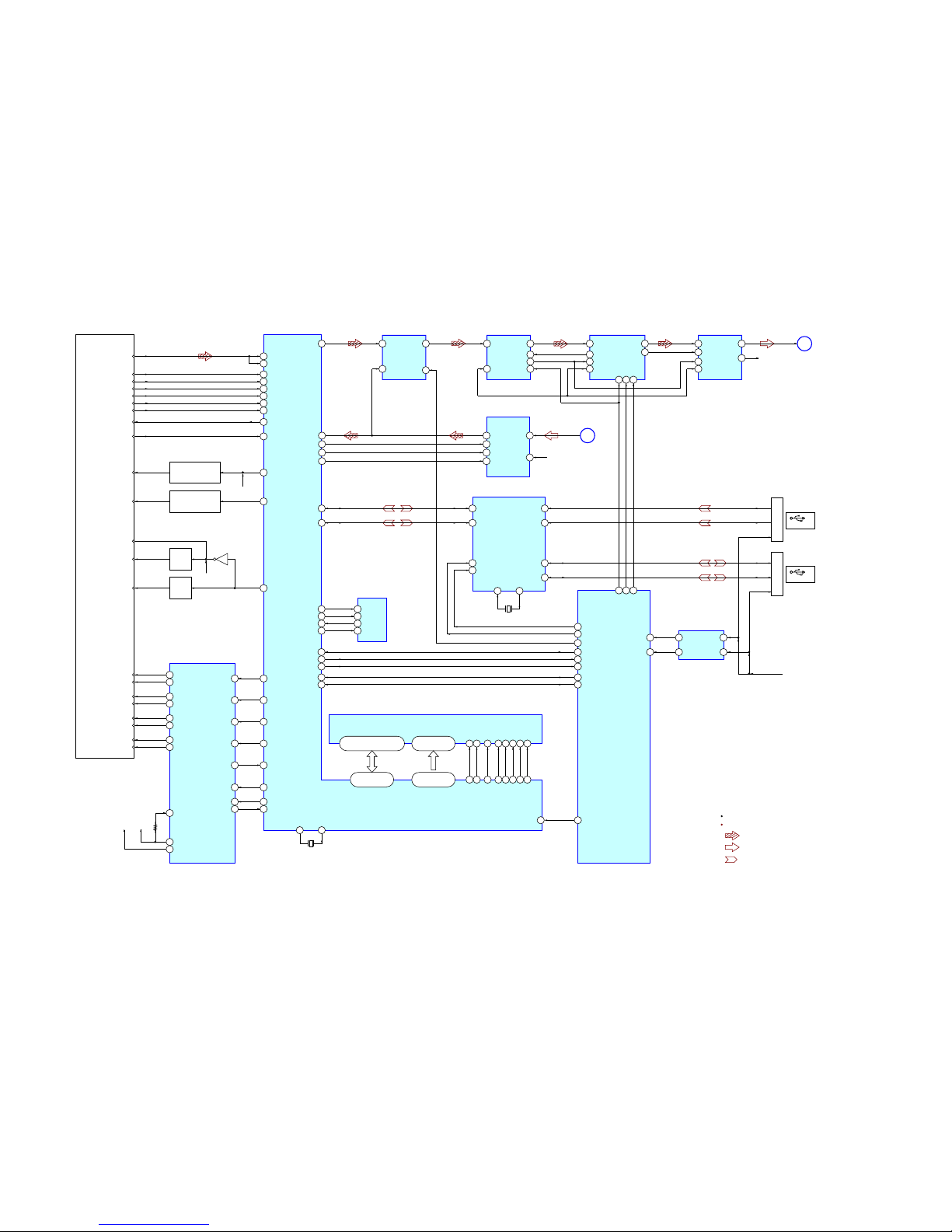
5-1. BLOCK DIAGRAM – CD/USB Section –
A
B
DEVICE, OPTICAL
RF AMP, SERVO DSP,
AUDIO PROCESSOR
IC501
SYSTEM
CONTROLLER
IC500 (1/4)
FOCUS/TRACKING COIL DRIVE,
SPINDLE/SLED MOTOR DRIVE
IC801
AUTOMATIC POWER
CONTROL
Q606
RF IP123
RF_C1
RF_B
128
RF_A
127
RF_D2
RF
VOA/A
VOB/B
VOC/C
VOD/D
RF_F4VOE/E+G
RF_E3VOF/F+H
V2O
10
VC
LDO114LD (780)
AUTOMATIC POWER
CONTROL
Q605
LDO215LD (650)
FOO22
CD ON
SWITCH
Q604-1
CD ON
SWITCH
Q604-2
VR (780)
MSW20VR (650)
FCS+
MSW
MDI113PD
Q603
64M SDRAM
IC504
X501
27MHz
6
FCS–
7
24
TRO21
TRK+
9
TRK–
8
23
FMO18
SL+ 10
SL– 11
22
DMO17
SP+ 12
SP– 13
39
2
29
21
SPFG/OPINN12627
DG0, DQ1 – DQ15
RD0 – RD15
PRST #
A0 – A11
RA0 – RA11
2, 4, 5, 7, 8, 10, 11, 13, 42,
44, 45, 47, 48, 50, 51, 53
52 – 55, 57 – 60,
69 - 62
90 - 92, 79 - 74,
88, 73
23 – 26,
29 – 34, 22, 35
XTALI
7
BA0 BA0
85
20
BA1 BA1
86
21
RCLK CLK
72
38
DQM0 LDQM
61
15
DQM1 UDQM
70
39
RAS# RAS
83
18
CAS# CAS
82
17
RWE# WE
80
16
MUTE1234533
MUTE41934
2335
38
REGO2
REGO1
REGO2
REGO1
(CMS-S76RFS3G)
XTALO
8
USB CONTROLLER
IC700
31
USBUP_DP
30
USBUP_DM
USB_DP 25
USB_DM 24
2USBDN1_DP
1USBDN1_DM
28HUB-OC2
CN1201
3
2
1
D+
D–
84
HUB-OC1
VBUS
USB
COMPARATOR
IC702
4USBDN2_DP
3USBDN2_DM
3
2
1
D+
D–
VBUS
MTK-RST40
MTK-OSD
35
MTK-SI
36
MTK-CLK
37
MTK-XIFCS
41
MTK-BUSY
38
IFSDI 40
IFSDO 35
IFSCK 34
IFCS# 42
IFBSY 41
HUB-RESET
83
HUB-VBUS-DETECT
82
VBUS_DET27
RESET_N26
X700
24MHz
XTAL1/
CLKIN
33
XTAL2
32
VBUS +5V
PLAY
CN1202
OPOUT124
1
7
3
5
SF_CS#
CS_
30
1
SF_CK
SCK
33
6
FLASH ROM
IC502
SO
2
SI
5
SF_DO
31
SF_DI
32
ACLK
ALRCK
ABCK
ADIN
118
L-OUT
ASDA
TA0
113
14
13
A/D CONVERTER
IC721
8
L-IN
R-CH
117
7
112
6
106
9
VOUT L
8
7
VOUT L
D/A CONVERTER
IC763
2
DATA
1
BCK
3
LRCK
16
SCK
23
27
DSP
IC762
11
22
19
21
25
23
24
13
ASYNCHRONOUS SAMPLE
RATE CONVERTER
IC761
4
14
7
MULTIPLEXER
IC741
6
5
R-CH
25
27 47 48
32 15 16
SDIN1
SDA1
SCL1
LRCK
MCLKO
SCLKOUT1
SCLKOUT2
SDOUT1
/RESET
2
RCKI
SDIN
/RST
SDOUT
LRCKO
BCKO
1C0
1C1
1Y
A
SCKI
LRCK
BCK
DOUT
VINL
VINR
ASEL
DSP-DATA
DSP-CLK
DSP-RESET
A
REC/PLAY
B
VO1+
VO1-
VO2-
VO2+
VO3+
VO3-
VO4+
VO4-
IN1
IN2
IN3
IN4
VSPDL
MUTE123
MUTE4
TSDM
OPIN-
REGVAR
REG5
TSD_M
(Page 24)
(Page 24)
: CD PLAY
: AUDIO
: USB
SIGNAL PATH
R-ch is omitted due to same as L-ch.
HCD-GPX5G/GPX7G/GPX8G
HCD-GPX5G/GPX7G/GPX8G
2424
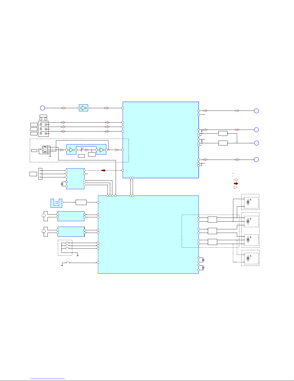
5-2. BLOCK DIAGRAM – MAIN Section –
TUNER (FM/AM)
IC101
FRF1
ARF1
LOUT
ROUTDAR-CH
CK
ANTENNA
FM/AM
RDSI
75
ST-RDS
42
ST-L15
14
21
DATA22CLK
46
MIC
26
OUTL
39 GAME_L
77
ST-DATA
78
ST-CLK
AUDIO DATA
86
AUDIO CLK
87
MIC DETECT
18
25
SWOUT
28
BB1L
38
INGAIN OUT L
27
BB2L
BASS AGC
Q900
INPUT SELECTOR,
ELECTRICAL VOLUME
IC806
SYSTEM CONTROLLER
IC500 (2/4)
: AUDIO
SIGNAL PATH
R-ch is omitted due to same as L-ch.
: TUNER (FM/AM)
J1300
MIC IN
RV1300
MIC LEVEL
MIN MAX
MIC AMP
IC1301
L-OUT
L-IN
OUTL
SW OUT L
BASS AGC
: MIC
1375
(Page 23)
13X-OUT
15X-IN
X701
8MHz
11XC-OUT
10XC-IN
X702
32.768kHz
(Page 23)
(Page 25)
(Page 25)
(Page 25)
13
OP AMP
IC901
4
6
13
10
8
A
E
D
C
B
MIC DRIVE
Q1302,Q1301
AUDIO IN
R-CH
43
GAME-LEFT
R
L
J500
PC/
GAME
R-CH
45
DVD LEFT
R-CH
DVD/
SAT
TV
40
TV LEFT
FRF2
7
CN103
R-CH
5
INGAIN OUT R
19
OUTR
18
BB1R
17
BB2R
BASS AGC
Q950
R-CH
20
AGCOUTR
23
R-CH
AGCOUTL
M
FIN
RIN
OUT2
OUT1
M751
(LOADING)
M
FIN
RIN
OUT2
OUT1
M741
(TABLE)
52
44
43
TABLE ADDRESS SENSOR
IC731
LD MOTOR DRIVER
IC701
3
7
9
2
4
TBL MOTOR DRIVER
IC712
RE701
ROTARY ENCORDER
7
9
2
4
LM-F
LM-R
46
45
TM-F
TM-R
49
50
E-1
E-2
51
E-3
53
ADDRESS SENSOR
SWITCH
Q731
TBL-SENS
(DISK TRAY ADDRESS DETECT)
S751
(OPEN/CLOSE DETECT)
22
FR-SPK-LED-RED
24
LED
DRIVER
Q707
D1800
(RED)
D1801
(BLUE)
3
4
LED
DRIVER
Q704
28
30
LED
DRIVER
Q709
D001
(R,G,B)
D001
(R,G,B)
FR-SPK-LED-BLUE
FR-SPK-LED-GREEN
SW-SPK-LED-GREEN
SW-SPK-LED-RED
SW-SPK-LED-BLUE
GPX7G/GPX8G
GPX7G
GPX7G
GPX8G
GPX7G/GPX8G
HIGH SPAKER (L,R)
FRONT SPAKER (L,R)
SUBWOOFER (L,R)
LOW SPAKER (L,R)
OPEN SW
19
X2
18
X1
X101
32.768kHz
D1800
(RED)
D1801
(BLUE)
HCD-GPX5G/GPX7G/GPX8G
HCD-GPX5G/GPX7G/GPX8G
2525
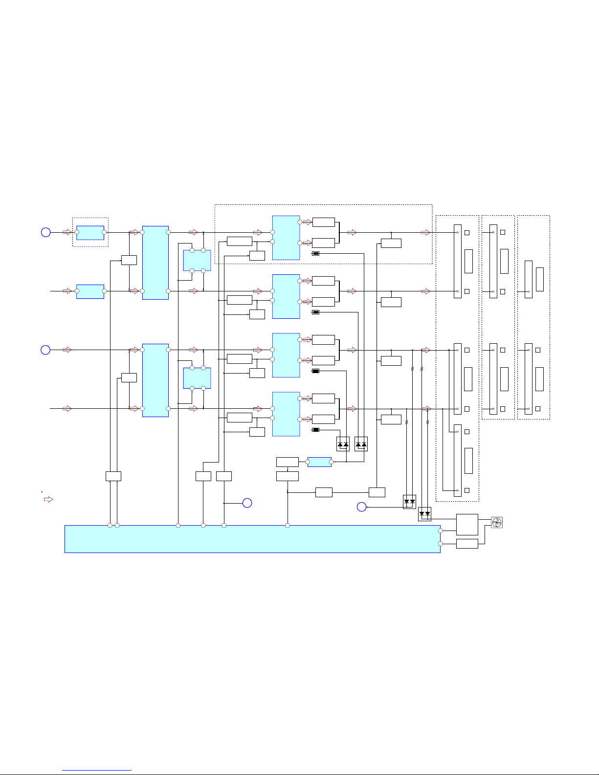
5-3. BLOCK DIAGRAM – AMP Section –
TB1400
FAN-LOCK
3
2
14
11
POWER AMP
IC1406
3
5
IN
HO
CSD
LO
PROTECTION
Q1443,1454
BOOSTER
Q1422
TH1400
RESET
SWITCH
Q1414
MUTE
SWITCH
Q954
CEC DATA SWITCH
Q1412
14
11
POWER AMP
IC1407
3
5
IN
HO
CSD
LO
PROTECTION
Q1444,1455
TH1401
SUBWOOFER
,03('$1&(86(ȍ
R
L
RESET
SWITCH
Q1415
CEC DA
TA SWITCH
Q1413
PREAMP
IC1403
CLOCK
IC1410
CLOCK
IC141
1
1
7
25AOUTINA-
INB+
BOUT
TB4002
3
2
14
11
POWER AMP
IC1408
3
5
IN
HO
CSD
LO
PROTECTION
Q1445,1456
TH1402
RESET
SWITCH
Q1416
MUTE
SWITCH
Q902
CEC DA
TA SWITCH
Q1411
14
11
POWER AMP
IC1409
3
5
IN
HO
CSD
LO
PROTECTION
Q1446,1457
TH1403
FRONT SPEAKERS
,03('$1&(86(ȍ
R
L
RESET
SWITCH
Q1417
CEC DA
TA SWITCH
Q1410
PREAMP
IC1404
1
7
25AOUTINA-
INB+
BOUT
DC FAN
FAN MOTOR LOCK
Q1447
F
AN MOTOR DRIVE
Q1439, Q1441,
Q1451, Q1453,
Q1458
SYSTEM CONTROLLER
IC500 (3/4)
D1435
D1403
69
61
PROTECTION
Q1448
PROTECTION
Q1449
OTP
DRIVE
Q1469, 1470
OTW DRIVE/
SD-SLOW DRIVE
Q1405
SWITCH
DRIVER
Q1407
MUTE
DRIVE
Q802
COMPARATOR
IC1405
21
7471
81
75
13
75
13
AOUT
INA+ INB+
BOUT
AOUT
INA+ INB+
BOUT
26
1
SW BPF-L
IC900
5
SW OUT L
R-CH
R-CH
OUTL
SW BPF-R
IC950
OUT IN
DAMP-CLK
FRONT-MUTE
DAMP-RESET
/SD-SLOW
FAN-DRIVE
OUTPUT
INPUT+
: AUDIO
SIGNAL
PATH
80
SW-MUTE
1
5
OUTPUT
INPUT+
70
DAMP-OCP
SWITCH
DRIVER
Q1474
BOOSTER
Q1423
BOOSTER
Q1418
BOOSTER
Q1419
BOOSTER
Q1420
BOOSTER
Q1421
BOOSTER
Q1424
BOOSTER
Q1425
D1417 D1419
TB4001
3
2
SATELLITE SPEAKERS
,03('$1&(86(ȍ
R
L
GPX8G
TB1400
3
2
SPEAKERS LOW
,03('$1&(86(ȍ
R
L
TB4002
3
2
SPEAKERS HIGH
,03('$1&(86(ȍ
R
L
TB1403
2
SUBWOOFER
,03('$1&(86(ȍ
TB4002
3
2
FRONT SPEAKERS
,03('$1&(86(ȍ
R
L
GPX7G
GPX5G
BASS AGC
GPX8G
GPX8G
(Page 24)
D
(Page 24)
C
(Page 26)
G
(Page 24)
E
HCD-GPX5G/GPX7G/GPX8G
HCD-GPX5G/GPX7G/GPX8G
2626
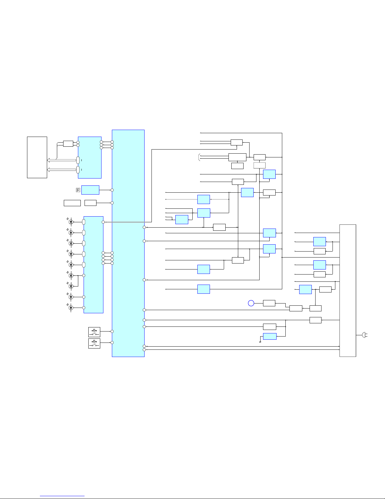
5-4. BLOCK DIAGRAM – PANEL/POWER SUPPLY Section –
REGULATOR,
SWITCHING
+5.0V REG
Q1477
+13V
+53V
+18V
+5.0 V
-18V
-5.0V
-53V
-40V
-VL
-VH
AC-DET
MAIN ON
SUB ON
+18V
REGULATOR
IC1414
-18V
REGULATOR
IC1415
-40V
REGULATOR
IC1402
DC-DC CONVERTER
T1001
OSC
Q1004, Q1005
SWITCH
Q716
+3.3V
REGULATOR
IC652
+5V
REGULATOR
IC701
M +9V
REGULATOR
IC802
A +9V
REGULATOR
IC803
VBUS +5V
REGULATOR
IC800
+1.8V
REGULATOR
IC651
D +3.3V
REGULATOR
IC801
AMP RESET
Q1402, Q1460
RESET
Q1475
μCOM RESET
Q506
μCOM RESET
IC508
SWITCH
Q702
SWITCH
Q701
SWITCHING
Q1401
BUFFER
Q507
SWITCH
DRIVER
Q703
SWITCH
Q806, Q807
-5.0V REG
Q1478
REGURATOR
Q1400
(AC IN)
DVDD +1.8V
DVDD +3.3V
D +3.3V
VBUS +5V
RF +3.3V
DVDD +5V
AVDD +5V
D +9V
VM +9V
M +9V
VACUUM
FLUORESCENT
DISPLAY
+13V
LED +13.5V (SEL A)
SYSTEM CONTROLLER
IC500 (4/4)
95
ROTARY
ENCODER
S1250
1
7
6
2
DJ CONTROL/
MASTER VOLUME
D1018 - D1021
(LEFT
TOP ILLUMINATION)
LED DRIVE
IC1002
14
19
65
63
12
79
25
43
68
4
5
6
8
VACUUM
FLUORESCENT
DISPLAY
FL1001
FLUORESCENT DISPLAY
DRIVER
IC1001
35 – 47
191
290
389
10 – 33
BUFFER
Q1001
48
49
REMOTE CONTROL
RECEIVER
IC1003
5 SIRCS
VBUS-OE
MTK-POWER-CTL
PCONT
-PSAVE-PROTECT
(SUB ON)
/SD-FAST
RESET
AC-CUT
PCONT-7V-13.5V (PCONT SUB)
PCONT-DAMP (MAIN ON)
FL-DATA
FL-CLK
MASTER-VOLUME
LED-LATCH
LED-DATA
LED-DRIVER-OE
LED-CLK
FL-CS
SG1/KS1
STB
DIN
CLK
SG24/KS24
GR2
GR14
GR15
GR16
GRIDS 1-16
SEGMENTS 1-24
DATA
/OE
LATCH
CLOCK
Q9, Q8
Q4, Q3
Q6, Q5
S1001 - S1005,
S1180 - S1184
67
AD-KEY0
S1006 - S1010,
S1210 - S1218
92
AD-KEY1
+VH
+VL
AVDD +3.3V
+4V
REGULATOR
IC804
EVER +4V
SWITCH
Q715
+3.3V
REGULATOR
IC103
TU +3.3V
DINAMIC LED
DRIVING
Q1006 - Q1009
SEL A :
DISPLAY BOARD
D1008, D1009, D1012, D1013, D1016, D1017,
D1018, D1019, D1022, D1023, D1027
USB BOARD
D1218, D1224
SEL B:
DISPLAY BOARD
D1006, D1007, D1010, D1011, D1014, D1015,
D1020, D1021, D1024, D1026
USB BOARD
D1216, D1221, D1223
GR15
GR16
23,24
D1006 - D1009
(RIGHT TOP ILLUMINATION)
D1022 - D1024, D1026, D1027
(CENTER ILLUMINATION)
21, 22
1, 2, 17
18, 1911, 12
15
16
D1014 - D1017
(LEFT BOTTOM ILLUMINATION)
D1010 - D1013
(RIGHT BOTTOM ILLUMINATION)
D1223
(USB B)
D1224
(USB A)
D1221
(DJ EFFECT)
D1216, D1218
(BASS BAZOOKA)
Q1, Q2, Q10
Q15, Q16
Q13
Q12
Q11
20
Q7
LED +13.5V (SEL B)
(Page 25)
G
HCD-GPX5G/GPX7G/GPX8G
HCD-GPX5G/GPX7G/GPX8G
2727
• Circuit Boards Location
TUNER1AM3R board
MAIN board
REGULATOR, SWITCHING board
4CH DAMP board
DMB22 board
SWITCH board
MOTOR (LD) board
MOTOR (TB) board
DRIVER board
SENSOR board
USB board
VOLUME board
DISPLAY board
MIC board (for GPX7G/GPX8G)
THIS NOTE IS COMMON FOR PRINTED WIRING BOARDS AND SCHEMATIC DIAGRAMS.
(In addition to this, the necessary note is printed in each block.)
For Schematic Diagrams.
Note:
• All capacitors are in μF unless otherwise noted. (p: pF) 50
WV or less are not indicated except for electrolytics and
tantalums.
• All resistors are in Ω and 1/4 W or less unless otherwise
specifi ed.
• f : Internal component.
• 2 : Nonfl ammable resistor.
• 5 : Fusible resistor.
• C : Panel designation.
• A
: B+ Line.
• B : B– Line.
• Voltages and waveforms are dc with respect to ground
under no-signal (detuned) conditions.
no mark : TUNER (FM)
* : Impossible to measure
• Voltages are taken with VOM (Input impedance 10 M).
Voltage variations may be noted due to normal production
tolerances.
• Waveforms are taken with a oscilloscope.
Voltage variations may be noted due to normal production
tolerances.
• Circled numbers refer to waveforms.
• Signal path.
F : AUDIO
f : TUNER (FM/AM)
N : MIC
J : CD PLAY
E : USB
• Abbreviation
E4 : African model
E2 : 120V AC area in E model
E51 : Chilean and Peruvian models
MX : Mexican model
For Printed Wiring Boards.
Note:
• X : Parts extracted from the component side.
• Y : Parts extracted from the conductor side.
• f : Internal component.
• : Pattern from the side which enables seeing.
(The other layers’ patterns are not indicated.)
Caution:
Pattern face side:
(SIDE B)
Parts face side:
(SIDE A)
Parts on the pattern face side seen
from the pattern face are indicated.
Parts on the parts face side seen from
the parts face are indicated.
Note: The components identifi ed by mark 0 or dotted
line with mark 0 are critical for safety.
Replace only with part number specifi ed.
Caution:
Pattern face side:
(Conductor Side)
Parts face side:
(Component Side)
Parts on the pattern face side seen
from the pattern face are indicated.
Parts on the parts face side seen from
the parts face are indicated.
• Abbreviation
E4 : African model
E2 : 120V AC area in E model
E51 : Chilean and Peruvian models
MX : Mexican model
HCD-GPX5G/GPX7G/GPX8G
HCD-GPX5G/GPX7G/GPX8G
2828
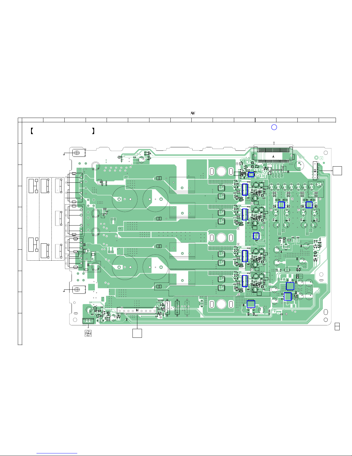
5-5. PRINTED WIRING BOARD –
4CH DAMP
Board (Component side) –
• See page 27 for Circuit Boards Location. • : Uses unleaded solder.
C1668
C1667
C1666
C1665
C1500
C1501
C1502
C1503
C1504
C1505
C1506
C1507
C1508
C1509
C1510
C1511
C1512
C1513
C1514
C1515
C1516
C1517
C1518 C1519
C1520
C1521
C1522
C1523
R1500
R1501
R1506
R1507
R1508
R1509
R1510
R1704
R1705
R1511
R1512
R1706
R1707
R1513
R1514
R1515
R1709
R1516
R1517
R1518
R1901
R1519
L1400
L1401
R1711
L1402
L1403
L1404
R1520
R1908
L1405
R1521
R1715
L1406
R1522
R1716
L1407
R1523
R1717
R1524
R1718
L1408
R1525
R1526
R1527
R1528
R1529
R1722
R1723
R1724
R1530
R1725
R1531
R1532
R1533
TB1400
R1728
R1534
R1535
R1729
R1536
R1537
R1538
R1539
ET1400
ET1401
R1731
R1540
R1541
1
9
R1542
R1543
16 3
R1544
R1545
R1546
R1547
R1548
R1549
C1572
C1574
R1550
R1551
R1746
R1747
R1554
R1555
R1556
R1557
R1558
R1559
C1584
R1560
R1561
R1562
R1563
R1564
R1565
R1566
R1567
R1568
R1569
R1570
R1571
R1572
R1573
R1960
R1777
R1780
R1785
1
3
CN1405
C1400
C1401C1402
B
E
Q1400
C1405
C1406
C1
B1
E1
C2
B2
E2
Q1402
C1407
C1408
C1409
C1
B1E1C2
B2E2
Q1405
C1
B1E1C2
B2E2
Q1407
C1410
C1411
C1605
C1412
C1606
C1413
C1607
C1414
Q1410
C1608
C1415
Q1411
C1416
Q1412
Q1413
C1
B1E1C2
B2E2
Q1414
C1B1
E1C2B2
E2
Q1415
C1
B1E1C2
B2E2
Q1416
C1
B1E1C2
B2E2
Q1417
Q1418
Q1419
C1614
Q1420
C1619
Q1421
Q1422
C1427
Q1423
Q1424
C1429
Q1425
C1620
D1408
D1409
C1430
O
I
IC1402
C1629
C1435
‚P
‚S
‚T ‚W
IC1405
C1436
1
16 9
8
IC1406
D1412
C1437
D1413
1
16 9
8
IC1407
D1414
1
16 9
8
IC1408
C1439
1
16 9
8
IC1409
D1415
R1607
R1608
Q1439
C1440
C1634
R1418
TH1400
C1441
R1419
14
58
IC1411
TH1401
C1442
TH1402
TH1403
OI
IC1414
B
E
Q1441
O
I
IC1415
R1420
R1421
R1422
Q1447
R1423
Q1448
R1619
Q1449
R1425
C1450
R1810
R1811
C1645C1646
C1647
D1430
C1648
R1621
Q1451
R1622
Q1453
C1457
R1430
C1458
D1435
C1459
Q1458
D1438
D1439
R1436
R1437
C1460
R1438
C1461
R1439
C1462
C1463
C1658
R1630
Q1460
D1442
D1443
C1468
D1444
R1440
C1469
R1441
R1442
R1443
R1638
C1660
D1448
R1444
BE
Q1469
D1449
R1445
R1446
R1447
C1470
TB4001
C1471
R1449
TB4002
C1473
Q1470
C1474
C1475
C1476
C1477
D1454
R1450
C1478
C1479
Q1475
D1455
D1456
R1647
B
E
Q1477
D1457
B
E
Q1478
R1457
C1480
R1458
C1481
R1459
C1482
C1483
C1484
C1485
C1486
C1487
R1654
C1488
R1460
C1489
R1461
R1462
R1657
R1463
R1464
R1465
R1467
C1490
R1468
C1491
R1469
C1492
C1493
C1494
C1495
R1662
C1496
C1497
R1663
C1498
R1470
R1664
C1499
R1471
R1665
R1667
R1473
R1474
JR1400
JR1401
JR1402
R1672
R1673
R1480
R1481
R1676
R1482
R1483
R1484
R1679
R1485
R1486
R1487
R1488
R1489
R1680
R1681
R1682
R1683
R1490
R1491
R1492
R1494 R1495
R1496
R1497
R1498
R1499
R1698
LP1400
LP1402
R1620
TB1403
Q1474
R1623
R1624
29
30
128
R1409
R1687
R1412
R1413
R1410
C1424
C1425
C1431
C1432
D1421
D1422
D1423
D1424
D1425
D1426
D1427
D1428
R1976
F1690
F1691
‚W
‚P ‚S
‚T
IC1403
‚W
‚P ‚S
‚T
IC1404
R1978
R1979
C1456
R1448
R1424
R1435
CN1400
C1615
GPX8G
GPX8G
GPX8G
GPX8G
GPX5G/7G
GPX8G
GPX5G/7G
GPX8G
GPX7G
GPX7G
GPX7G
GPX8G
GPX8G
GPX5G
GPX7G/8G
NO1403
NO1402
B
MAIN
BOARD
CN805
(Page 35)
DC FAN
4CH DAMP BOARD (Component Side)
1 2 3 4 5 6 7 8 9 10 11 14 1512 13
A
B
C
D
E
F
G
H
I
J
1-885-760-
21
(21)
+ –+ –
+ –+ –+ –
+ –
(CHASSIS)
(CHASSIS)
FRONT SPEAKERS
L R
SATELLITE SPEAKERS
L
R
SUBWOOFER
L
R
SUBWOOFER
,03('$1&(86(ȍ
R
L
FRONT SPEAKERS
,03('$1&(86(ȍ
R
L
GPX8G
GPX7G
GPX5G
SPEAKERS
,03('$1&(86(ȍ
,03('$1&(86(ȍ,03('$1&(86(ȍ
,03('$1&(86(ȍ
HIGH
L R
SPEAKERS
,03('$1&(86(ȍ
LOW
L R
CONNECT TO
SWITCHING
REGULATOR
BOARD
(NOT SUPPLIED)
CONNECT TO
SWITCHING
REGULATOR
BOARD
(NOT SUPPLIED)
Ver. 1.1
HCD-GPX5G/GPX7G/GPX8G
HCD-GPX5G/GPX7G/GPX8G
2929
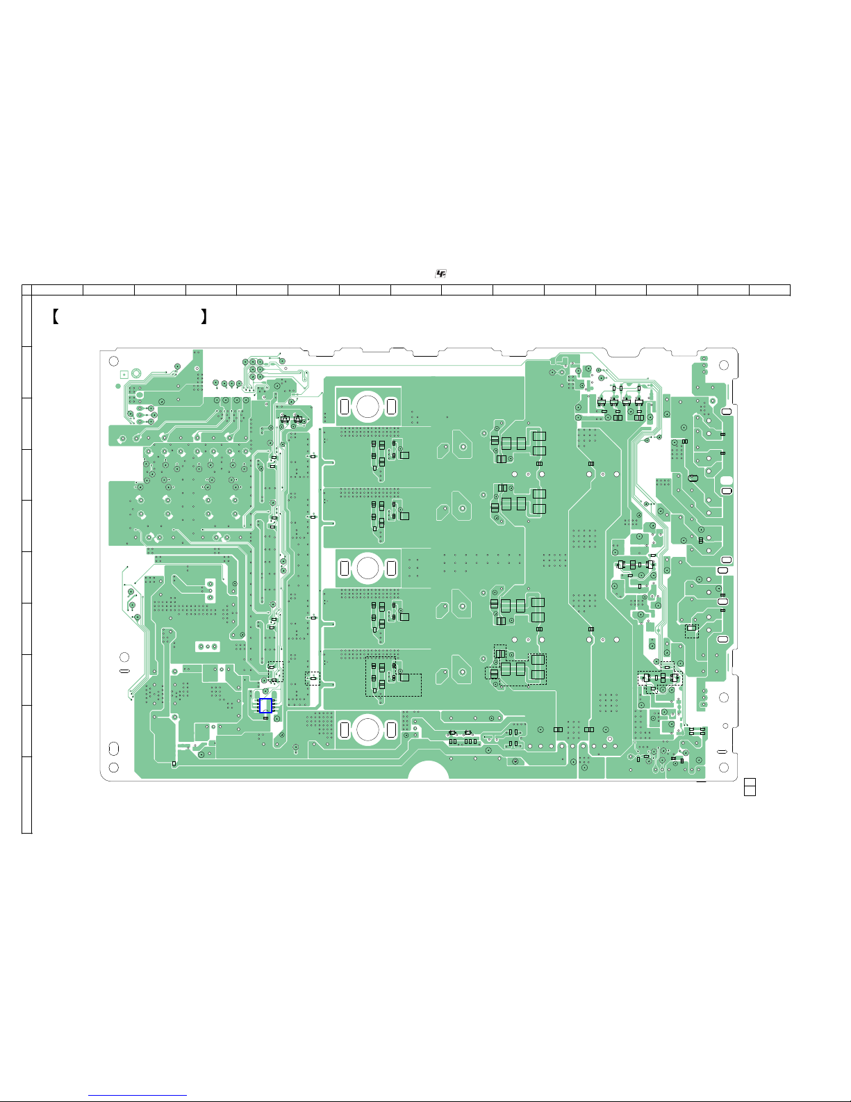
5-6. PRINTED WIRING BOARD –
4CH DAMP
Board (Conductor side) –
• See page 27 for Circuit Boards Location. • : Uses unleaded solder.
C1585
C1588
C1524
C1525
C1526 C1527
C1528
C1529
R1502
R1503
R1504
R1505
JL1563
JL1564
C1530
C1531
JL1565
JL1566
C1532
JL1567
C1533
C1534
C1535
R1701
C1536
C1537
C1538
C1539
R1708
C1540
C1541
C1542
C1543
C1544
R1710
C1545
C1546 C1547
R1910
R1911
R1912
R1913
C1578
R1744
C1579
R1745
C1580
C1581
C1582
R1750
R1751
R1758
R1759
R1760
R1954
R1761
R1955
R1762
R1956
R1763
R1957
R1764
R1765
R1574
R1575
R1576
R1577
R1578
R1579
R1772
R1580
R1775
R1581
R1781
R1782
R1783
R1784
R1592
R1594
JL1400
JL1401
JL1402
JL1403
JL1404
JL1405
JL1406
JL1407
JL1408
JL1409
JL1410
JL1411
JL1413
JL1414
JL1415
JL1416
JL1417
JL1418
JL1419
JL1420
JL1421
JL1422
JL1423
JL1424
JL1425
JL1426
JL1429
JL1430
JL1431
JL1432
JL1433
JL1434
JL1435
JL1436
JL1437
JL1440
JL1441
JL1442
JL1443
JL1444
JL1445
JL1446
JL1447
JL1448
JL1449
JL1450
JL1451
JL1452
JL1453
JL1454
JL1455
JL1456
C1616
JL1457
C1617
JL1458
C1618
JL1459
D1406
D1407
JL1460
JL1461
JL1462
JL1463
JL1464
JL1465
JL1466
JL1468
JL1470
JL1471
JL1472
JL1473
JL1474
1
4
58
IC1410
JL1476
R1803
R1806
Q1443
R1807
Q1444
R1808
Q1445
Q1446
R1618
JL1480
JL1481
C1643
JL1485
JL1487
JL1488
JL1489
Q1454
Q1455
Q1456
Q1457
JL1490
JL1491
JL1492
JL1493
JL1494
JL1495
JL1496
JL1498
C1662
C1664
R1642
R1643
R1653
R1655
R1660
R1661
R1668
R1669
R1475
R1476
R1477
R1478
R1670
R1671
JR1403
JL1502
JL1503
JL1506
JL1510
JL1514
JL1515
D1417D1419
JL1427
JL1399
R1625
C1567
C1569
C1568
C1566
C1627
C1626
C1625
C1628
JL1568
JL1569
JL1570
JL1571
JL1572
JL1573
JL1574
JL1575
JL1579
JL1585
JL1589
JL1594
JL1578
JL1586
JL1576
JL1595
JL1583
JL1588
JL1593
JL1580
JL1590
JL1596
JL1582
JL1592
JL1581
JL1591
JL1584
JL1577
JL1599
JL1603
JL1597
JL1606
JL1600
JL1604
JL1602
JL1601
JL1598
JL1605
JL1486
C1552
C1553
C1554
C1555
GPX8G
GPX8G
R1644
GPX7G
GPX8G
GPX8G
R1645
GPX8G
C1589
C1592
4CH DAMP BOARD
1 2 3 4 5 6 7 8 9 10 11 14 1512 13
A
B
C
D
E
F
G
H
I
J
1-885-760-
21
(21)
(Conductor Side)
Ver. 1.1
 Loading...