

Page 1
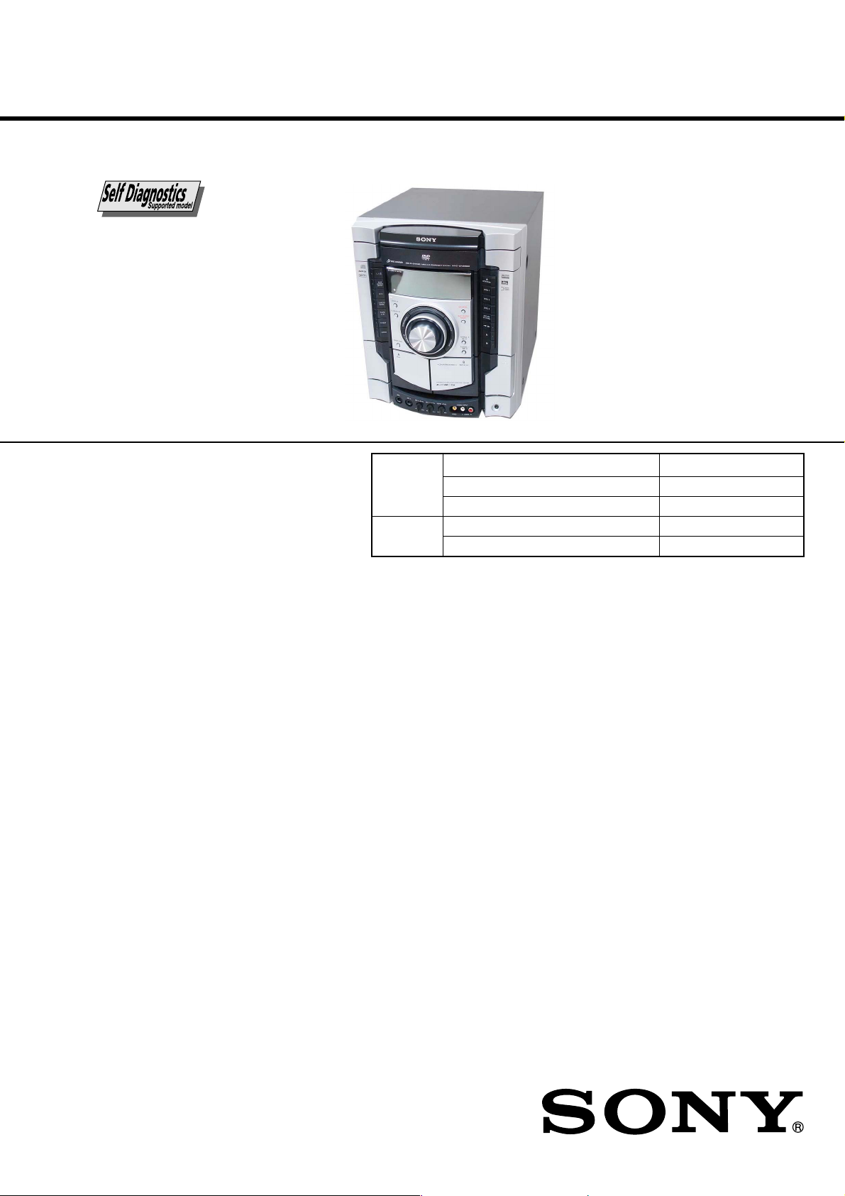
HCD-GN999D
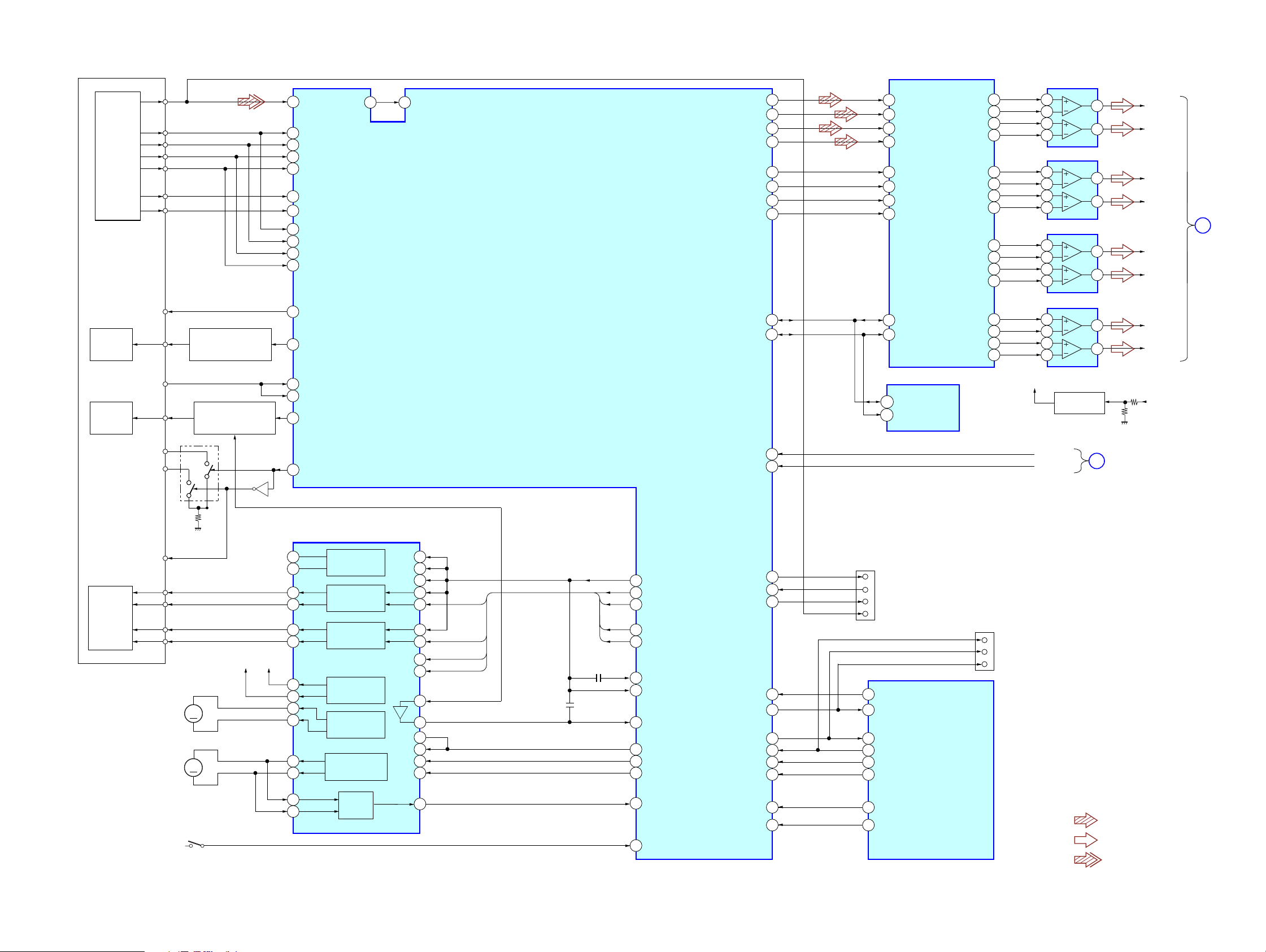
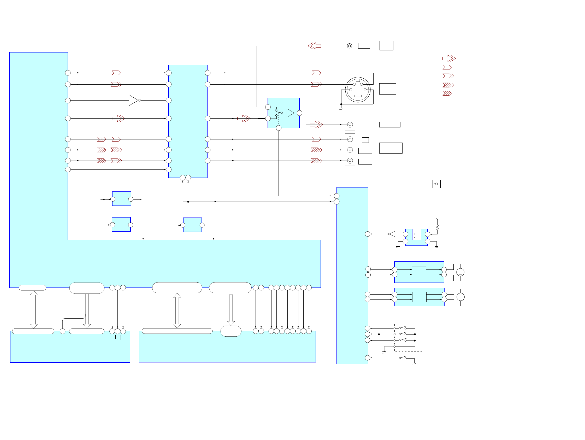
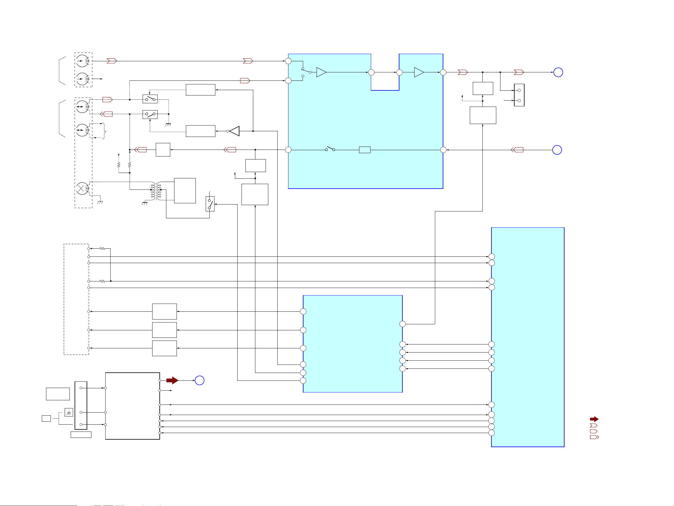
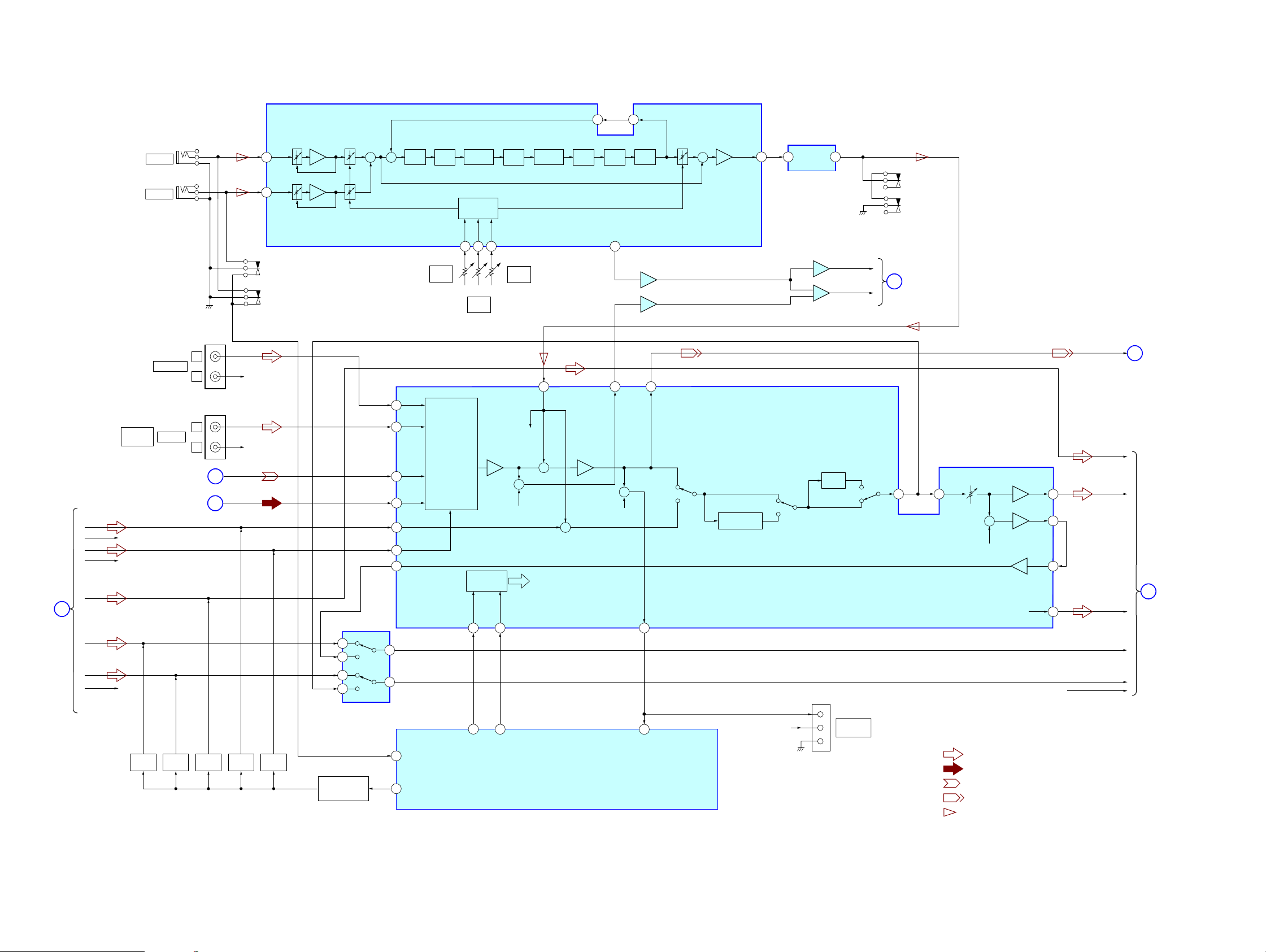
SERVICE MANUAL
Ver.1.0 2006.06
• HCD-GN999D is the Amplifier,
DVD player, tape deck and tuner
section in MHC-GN999D/GN999DS.
DVD
Section
TAPE Model Name Using Similar Mechanism NEW
Section Tape Transport Mechanism Type CWN42FR602
Model Name Using Similar Mechanism HCD-GNV99D
DVD Mechanism Type CDM74HF-DVBU101
Optical Pick-up Name KHM-310CAB/C2NP
E Model
SPECIFICATIONS
Amplifier section
The following are measured at AC 120, 127, 220,
240V, 50/60 Hz
DIN power output (rated) 135 W + 135 W
(6 ohms at 1 kHz, DIN)
Continuous RMS power output (reference)
Front speaker: 160 W + 160 W
(6 ohms at 1 kHz, 10% THD)
Center speaker: 50 W
(16 ohms at 1 kHz, 10% THD)
Surround speaker: 50 W + 50 W
(16 ohms at 1 kHz, 10% THD)
Subwoofer: 160 W (6 ohms at 100 Hz, 10% THD)
Inputs
VIDEO INPUT (phono jacks) VIDEO: 1 Vp-p, 75 ohms
AUDIO L/R: Voltage 250 mV,
impedance 47 kilohms
TV/SAT AUDIO IN L/R (phono jacks)
Voltage 250 mV/450 mV,
impedance 47 kilohms
MIC 1/MIC 2
(phone jack):
Sensitivity 1 mV,
impedance 10 kilohms
Outputs
VIDEO OUT (phono jack): Max. output level 1 Vp-p,
unbalanced, Sync.
negative load impedance
75 ohms
COMPONENT VIDEO OUT Y: 1 Vp-p, 75 ohms
PB/CB: 0.7 Vp-p, 75 ohms
PR/CR: 0.7 Vp-p, 75 ohms
S VIDEO OUT (4-pin/mini-DIN jack)
Y: 1 Vp-p, unbalanced,
Sync. negative
C: 0.286 Vp-p, load
impedance 75 ohms
PHONES (stereo mini jack): Accepts headphones of
8 ohms or more
FRONT SPEAKER: Use only the supplied speakers
SURROUND SPEAKER Use only the supplied speakers
CENTER SPEAKER Use only the supplied speakers
SUB WOOFER Use only the supplied subwoofer
Disc player section
System Compact disc and digital audio and
video system
Laser Semiconductor laser
(DVD: λ = 650 nm, CD: λ = 790 nm)
Emission duration: continuous
Frequency response DVD (PCM 48 kHz):
2 Hz – 22 kHz (±1dB)
CD: 2 Hz – 20 kHz (±0.5 dB)
Video color system format
Latin American models: NTSC
Other models: NTSC and PAL
Tape deck section
Recording system 4-track 2-channel stereo
Frequency response 50 – 13,000 Hz (±3 dB),
using Sony TYPE I tape
– Continued on next page –
MINI HI-FI COMPONENT SYSTEM
9-887-269-01
2006F02-1
© 2006.06
Sony Corporation
Home Audio Division
Published by Sony Techno Create Corporation
Page 2

HCD-GN999D
Tuner section
FM stereo, FM/AM superheterodyne tuner
FM tuner section
Tuning range 87.5 – 108.0 MHz (50 kHz step)
Antenna FM lead antenna
Antenna terminals 75 ohms unbalanced
Intermediate frequency 10.7 MHz
AM tuner section
Tuning range
Latin American models: 530 – 1,710 kHz
(with the interval set at 10 kHz)
531 – 1,710 kHz
(with the interval set at 9 kHz)
Saudi Arabian and Russian models:
531– 1,602 kHz
(with the interval set at 9 kHz)
Other models: 531 – 1,602 kHz
(with the interval set at 9 kHz)
530 – 1,710 kHz
(with the interval set at 10 kHz)
Antenna AM loop antenna
Antenna terminals External antenna terminal
Intermediate frequency 450 kHz
General
Power requirements
Mexican model: 127 V AC, 60 Hz
Saudi Arabian model: 120 – 127 V, 120 – 220 V or 220 –
240 V AC, 50/60 Hz
Adjustable with voltage selector
Thai model: 220 V AC, 50/60 Hz
Other models: 120 V or 220 – 240 V AC, 50/60 Hz
Adjustable with voltage selector
Power consumption 160 W
Dimensions (w/h/d) (Approx.) 280 × 326 x 385.5 mm
Mass (Approx.) 6.5 kg
Design and specifications are subject to change without notice.
Self-diagnosis Function
(When letters/numbers appear in the
display)
When the self-diagnosis function is activated to
prevent the system from malfunctioning, a
5-character service number (e.g. C 13 50) with a
combination of a letter and 4 digits appears on
the TV screen and the front panel display. In this
case, check the following table.
First 3
characters of
the service
number
C 13 This disc is dirty.
C 31 The disc is not inserted correctly.
E XX
(XX is a
number)
UNLEADED SOLDER
Boards requiring use of unleaded solder are printed with the leadfree mark (LF) indicating the solder contains no lead.
(Caution: Some printed circuit boards may not come printed with
the lead free mark due to their particular size)
Cause and corrective action
Clean the disc with a soft cloth
Restart the system, then re-insert
the disc correctly.
To prevent a malfunction, the system
has performed the self-diagnosis
function.
Contact your nearest Sony dealer or
local authorized Sony service
facility and give the 5-character
service number.
Example: E 61 10
.
: LEAD FREE MARK
Unleaded solder has the following characteristics.
• Unleaded solder melts at a temperature about 40 °C higher
than ordinary solder.
Ordinary soldering irons can be used but the iron tip has to be
applied to the solder joint for a slightly longer time.
Soldering irons using a temperature regulator should be set to
about 350 °C.
Caution: The printed pattern (copper foil) may peel away if
the heated tip is applied for too long, so be careful!
• Strong viscosity
Unleaded solder is more viscou-s (sticky, less prone to flow)
than ordinary solder so use caution not to let solder bridges
occur such as on IC pins, etc.
• Usable with ordinary solder
It is best to use only unleaded solder but unleaded solder may
also be added to ordinary solder.
2
Page 3

TABLE OF CONTENTS
HCD-GN999D
1. SERVICING NOTES ................................................ 4
2. GENERAL ................................................................... 5
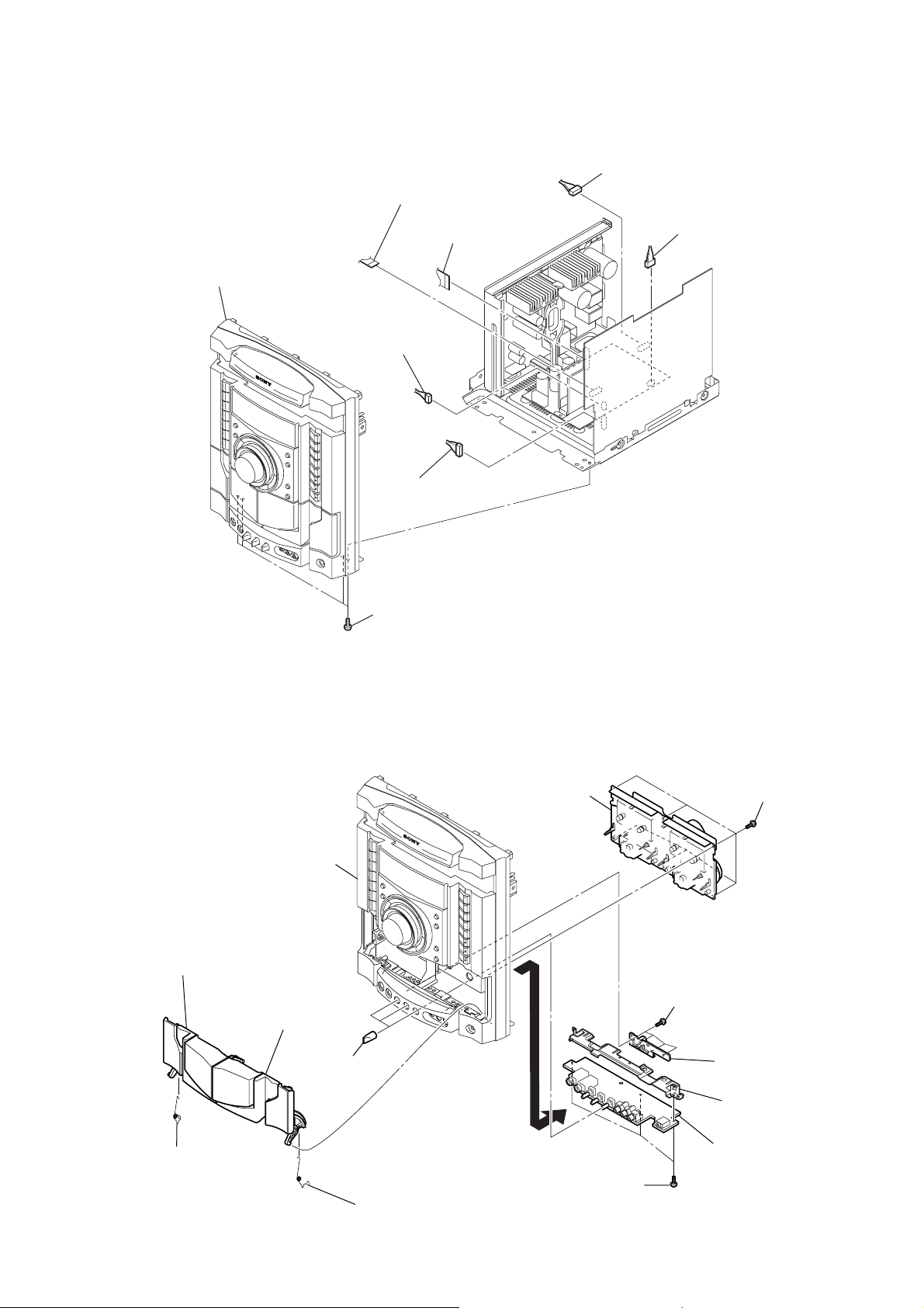
3. DISASSEMBLY
3-1. Disassembly Flow ........................................................... 7
3-2. Cabinet Steel case............................................................ 8
3-3. Loading Panel.................................................................. 8
3-4. Tuner Pack ....................................................................... 9
3-5. Back Panel, DC Fan (M891) ........................................... 9
3-6. DVD Mechanism Deck ................................................... 10
3-7. KARAOKE Board, VIDEO Board, DMB15 Board ........ 10
3-8. Front Panel Assy.............................................................. 11
3-9. Tape Mechanism Deck, MIC Board ................................ 11
3-10. PANEL Board, IR Board, VOL Board ............................ 12
3-11. MAIN Board, ADC Board ............................................... 12
3-12. POWER Board ................................................................ 13
3-13. SPEAKER Board, SMASTER Board ............................. 13
3-14. DRIVER Board, SW Board ............................................. 14
3-15. DVD Assy ........................................................................ 14
3-16. Optical pick-up ................................................................ 15
3-17. SENSOR Board ............................................................... 15
3-18. MOTOR (TB) Board ....................................................... 16
3-19. MOTOR (LD) Board ....................................................... 16
4. TEST MODE ............................................................... 17
5. MECHANICAL ADJUSTMENTS ......................... 21
6. ELECTRICAL ADJUSTMENTS .......................... 22
7. DIAGRAMS .......................................................... 25
7-1. Block Diagram – RF Section – ....................................... 27
7-2. Block Diagram – Video Section – ................................... 28
7-3. Block Diagram – Tape/Tuner Section – .......................... 29
7-4. Block Diagram – Main Section – .................................... 30
7-5. Block Diagram – AMP Section – .................................... 31
7-6. Block Diagram – Display/Power Section – ..................... 32
7-7. Printed Wiring Board – DMB15 Board (Side A) – ......... 33
7-8. Printed Wiring Board – DMB15 Board (Side B) – ........ 34
7-9. Schematic Diagram – DMB15 Board (1/4) – ................ 35
7-10. Schematic Diagram – DMB15 Board (2/4) – ................ 36
7-11. Schematic Diagram – DMB15 Board (3/4) – ................ 37
7-12. Schematic Diagram – DMB15 Board (4/4) – ................ 38
7-13. Printed Wiring Boards – CD Mechanism Section – ....... 39
7-14. Schematic Diagram – CD Mechanism Section – .......... 40
7-15. Printed Wiring Board – MAIN Board – .......................... 41
7-16. Schematic Diagram – MAIN Board (1/3) – ................... 42
7-17. Schematic Diagram – MAIN Board (2/3) – ................... 43
7-18. Schematic Diagram – MAIN Board (3/3) – ................... 44
7-19. Printed Wiring Board – Panel Section –.......................... 45
7-20. Schematic Diagram – Panel Section – ........................... 46
7-21. Printed Wiring Boards – MIC, VOL
And SPEAKER Boards – ................................................ 47
7-22. Schematic Diagram – MIC, VOL
And SPEAKER Boards – ................................................ 48
7-23. Printed Wiring Board – ADC Board – ............................. 49
7-24. Schematic Diagram – ADC Board – .............................. 50
7-25. Printed Wiring Board – SMASTER Board (Side A) – .... 51
7-26. Printed Wiring Board – SMASTER Board (Side B) – .... 52
7-27. Schematic Diagram – SMASTER Board (1/3) – ........... 53
7-28. Schematic Diagram – SMASTER Board (2/3) – ........... 54
7-29. Schematic Diagram – SMASTER Board (3/3) – ........... 55
7-30. Printed Wiring Board – VIDEO Board – ........................ 56
7-31. Schematic Diagram – VIDEO Board – .......................... 57
7-32. Printed Wiring Boards – POWER Board – ..................... 58
7-33. Schematic Diagram – POWER Board – ......................... 59
7-34. Printed Wiring Board – KARAOKE Board – ................. 60
7-35. Schematic Diagram – KARAOKE Board – ................... 61
7-36. IC Pin Function Description ............................................ 63
8. EXPLODED VIEWS
8-1. Case, Back Panel Section ................................................ 73
8-2. Front Panel Section ......................................................... 74
8-3. Chassis Section ................................................................ 75
8-4. DVD Mechanism Section-1 (CDM74HF-DVBU101) .... 76
8-5. DVD Mechanism Section-2 (CDM74HF-DVBU101) .... 77
9. ELECTRICAL PARTS LIST ....................... 78
3
Page 4
HCD-GN999D
SECTION 1
SERVICING NOTES
NOTES ON HANDLING THE OPTICAL PICK-UP BLOCK
OR BASE UNIT
The laser diode in the optical pick-up block may suffer electrostatic
break-down because of the potential difference generated by the
charged electrostatic load, etc. on clothing and the human body.
During repair, pay attention to electrostatic break-down and also
use the procedure in the printed matter which is included in the
repair parts.
The flexible board is easily damaged and should be handled with
care.
NOTES ON LASER DIODE EMISSION CHECK
The laser beam on this model is concentrated so as to be focused on
the disc reflective surface by the objective lens in the optical pickup block. Therefore, when checking the laser diode emission,
observe from more than 30 cm away from the objective lens.
LASER DIODE AND FOCUS SEARCH OPERATION
CHECK
Carry out the “S curve check” in “CD section adjustment” and check
that the S curve waveform is output several times.
CAUTION
Use of controls or adjustments or performance of procedures
other than those specified herein may result in hazardous
radiation exposure.
This appliance is classified as
a CLASS 1 LASER product.
This label is located on the rear
exterior.
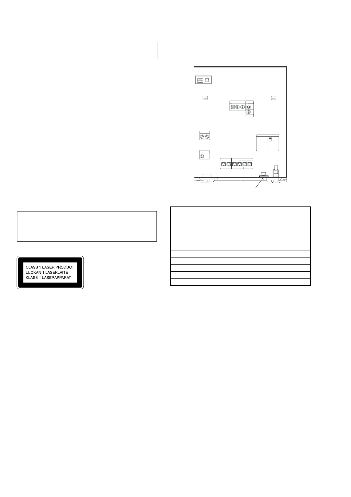
• MODEL IDENTIFICATION
– Back Panel –
PAR T No.
MODEL PART No.
E3, E15 models 2-658-971-0[]
E2 model 2-658-971-1[]
EA model 2-658-971-2[]
MY,SP models 2-658-971-3[]
E12 model 2-658-971-4[]
E13 model 2-658-971-5[]
PH model 2-658-971-6[]
MX model 2-658-971-7[]
E51 model 2-658-971-8[]
TH model 2-658-971-9[]
Notes on chip component replacement
• Never reuse a disconnected chip component.
• Notice that the minus side of a tantalum capacitor may be
damaged by heat.
Flexible Circuit Board Repairing
• Keep the temperature of soldering iron around 270˚C
during repairing.
• Do not touch the soldering iron on the same conductor of the
circuit board (within 3 times).
• Be careful not to apply force on the conductor when soldering
or unsoldering.
NOTE ON REPLACEMENT OF DMB15 BOARD
New part of EEPROM (IC103) on the DMB15 board cannot be
used. Therefore, if the mounted DMB15 board (A-1167-802-A or
A-1167-915-A or A-1188-872-A) is replaced, exchange new
EEPROM with that used before the replacement.
SAFETY-RELATED COMPONENT WARNING!!
COMPONENTS IDENTIFIED BY MARK 0 OR DOTTED LINE WITH
MARK 0 ON THE SCHEMATIC DIAGRAMS AND IN THE PARTS
LIST ARE CRITICAL TO SAFE OPERATION. REPLACE THESE
COMPONENTS WITH SONY PARTS WHOSE PART NUMBERS
APPEAR AS SHOWN IN THIS MANUAL OR IN SUPPLEMENTS
PUBLISHED BY SONY.
• Abbreviation
E2 : 120V AC Area in E model
E3 : 240V AC Area in E model
E12 : 220V-240V AC Area in E model
E13 : 220V-230V AC area in E model
E15 : Iran model
E51 : Chilean and Perurian model
EA : Saudi Arabia model
MX : Mexican model
MY : Malaysia model
PH : Philippines model
SP : Singapore model
TH : Thai model
4
Page 5
LOCATING THE CONTROLS
SECTION 2
GENERAL
HCD-GN999D
This section is extracted
from instruction manual.
ALPHABETICAL ORDER
A - D
CD SYNC 8
Deck A wk
Deck B qj
DIRECTION ea
DISC 1 ~ 3 q;
DISC SKIP/EX-CHANGE qa
Disc tray 7
DISPLAY r;
Display 4
DVD eh
E - O
ECHO LEVEL ws
EQ BAND/MEMORY 3
GROOVE qk
ILLUMINATION el
IR Receptor 2
MASTER VOLUME ql
MIC 1 (jack) wh
MIC 2 (jack) wg
MIC 1 LEVEL wf
MIC 2 LEVEL wd
Top view
P - Z
PHONES (jack) w;
Power illuminator wj
PRESET EQ wl
REC PAUSE/START 6
SOUND FIELD 5
SUB WOOFER ON/OFF ej
TAPE A/B ef
Tape lid qj wk
TUNER/BAND eg
TUNING +/– qh
TV/SAT ed
VIDEO es
VIDEO INPUT (jacks) wa
SYMBOLS
?/1 (on/standby) ek
Z OPEN/CLOSE 9
nN (play) qs
. OPERATION DIAL >
(go backward/forward) 1
mM (rewind/fast forward)
qh
qh
X (pause) qd
x (stop) qf
Z PUSH (Eject A) e;
Z PUSH (Eject B) qg
Front vi ew
r;
el
ek
ej
eh
eg
ef
ed
es
ea
e;
wl
wk
wj
34 5 6
2
1
7
8
9
q;
qa
qs
qd
qf
qg
qh
qj
qk
ql
w;
wh
wg
wf
wd
ws
wa
5
Page 6
HCD-GN999D
Remote control
ALPHABETICAL ORDER
A - L
ADVANCE wf
ALBUM +/– qa
ANGLE q;
AUDIO 8
CLEAR wk
DISC SKIP 3
DISPLAY ed
ENTER wh
FM MODE 7
FUNCTION +/– 4
KARAOKE MODE ea
KARAOKE PON e;
KEY CONTROL #/2 es
M - S
MENU qs
Numeric Buttons
PICTURE NAVI 6
PRESET + qh
PRESET – wd
REPEAT 7
REPLAY wf
SCORE 5
SLEEP eg
SLOW qj
SLOW ws
SOUND FIELD 5qd
STEP C wf
SUBTITLE 9
T - Z
THEATRE SYNC 1
TIMER MENU eh
TIME/TEXT ef
TOP MENU wj
TUNING + qj
TUNING – ws
TV2) w;
TV CH +
TV CH –2) wd
TV/VIDEO
TV VOL +/–
TV &/1 (on/standby)2) 2
VOLUME +/–
1)2)
wl
2)
qh
2)
eg
1)2)
qf
1)
qf
NUMBERS AND SYMBOLS
?/1 (on/standby) 2
x (stop) qk
X (pause) ql
1)
(play) wa
H
> (go forward) qh
. (go backward) wd
M (fast forward) qj
m (rewind) ws
V/v/B/b
10/0
-/--
O RETURN wg
c STEP wf
1)
2)
wh
2)
wl
2)
wk
DISPLAY qg
The numeric button 5, TV VOL +, VOLUME + and
H buttons have a tactile dot. Use the tactile dot as
a reference when operating the system.
This button is used to operate a Sony TV. For
details, see “Operating a Sony TV with the remote”
on page 17.
eh
eg
ef
ed
es
ea
e;
wl
wk
wj
wh
wg
wf
wd
ws
wa
w;
1
2
3
4
5
6
7
8
9
q;
qa
qs
qd
qf
qg
qh
qj
qk
ql
Setting the clock
1
Press ?/1 to turn on the system.
2
Press TIMER MENU.
The hour indication flashes in the display.
3
Press V or v repeatedly to set the
hour.
4
Press ENTER.
The minute indication flashes in the
display.
5
Press V or v repeatedly to set the
minute.
6
Press ENTER.
The clock starts functioning.
To adjust the clock
1
Press TIMER MENU.
“PLAY SET” flashes in the display.
2
Press V or v repeatedly to select "CLOCK
SET", then press ENTER.
The hour indication flashes in the display.
3
Do the same procedures as step 3 to 6
above.
Notes
The clock settings are canceled when you disconnect
the power cord or if a power failure occurs.
You cannot set the clock in Power Saving Mode
.
6
Page 7
• This set can be disassembled in the order shown below.
3-1. DISASSEMBLY FLOW
SET
HCD-GN999D
SECTION 3
DISASSEMBLY
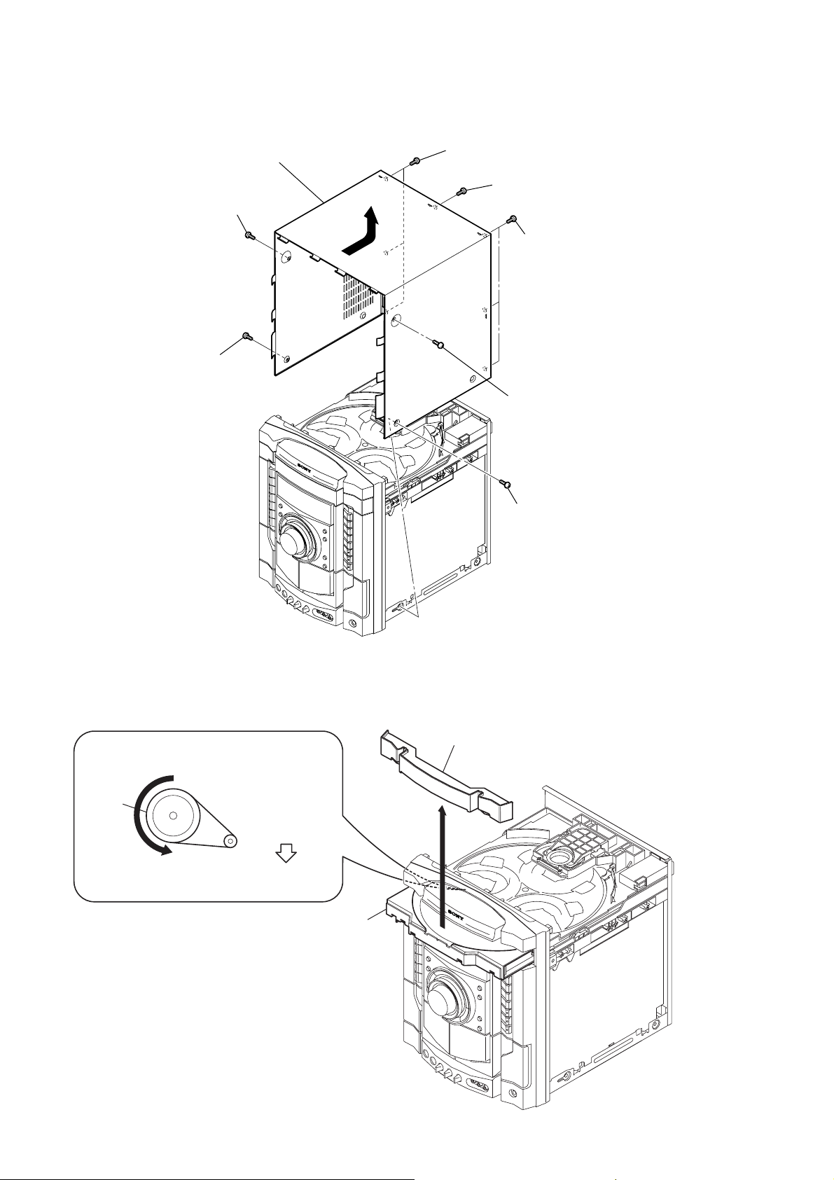
3-2. CABINET STEEL CASE
(Page 8)
3-3. LOADING PANEL
(Page 8)
3-4. TUNER PACK
(Page 9)
3-5. BACK PANEL,
DC FAN (M891)
(Page 9)
3-6. DVD MECHANISM DECK
(Page 10)
3-7. KARAOKE BOARD,
VIDEO BOARD,
DMB15 BOARD,
(Page 10)
3-8. FRONT PANEL ASSY
(Page 11)
3-11. MAIN BOARD,
ADC BOARD
(Page 12)
3-14. DRIVER BOARD,
SW BOARD
(Page 14)
3-9. TAPE MECHANISM DECK,
MIC BOARD
(Page 11)
3-12. POWER BOARD
(Page 13)
3-13. SPEAKER BOARD,
SMASTER BOARD
(Page 13)
3-15. DVD ASSY
(Page 14)
3-16. OPTICAL PICK-UP
(Page 15)
3-10. PANEL BOARD,
IR BOARD,
VOL BOARD
(Page 12)
3-17. SENSOR BOARD
(Page 15)
3-18. MOTOR (TB) BOARD
(Page 16)
3-19. MOTOR (LD) BOARD
(Page 16)
7
Page 8
HCD-GN999D
)
3-2. CABINET STEEL CASE
4
screw
(case 3 TP2)
(3×12)
3
screw
(case 3 TP2)
(3×8)
9
cabinet steel case
8
5
three screws
(+BVTP 3×8)
7
screw
(+BVTP 3×8)
2
(case 3 TP2)
(3×12)
6
three screws
(+BVTP 3×8
screw
3-3. LOADING PANEL
DVD mechanism deck (CDM74HF-DVBU101)
1
Turn the pulley to the arrow direction.
Pulley
Front side
3
loading panel
4
1
screw
(case 3 TP2)
(3×8)
2
Pull out disc tray.
8
Page 9
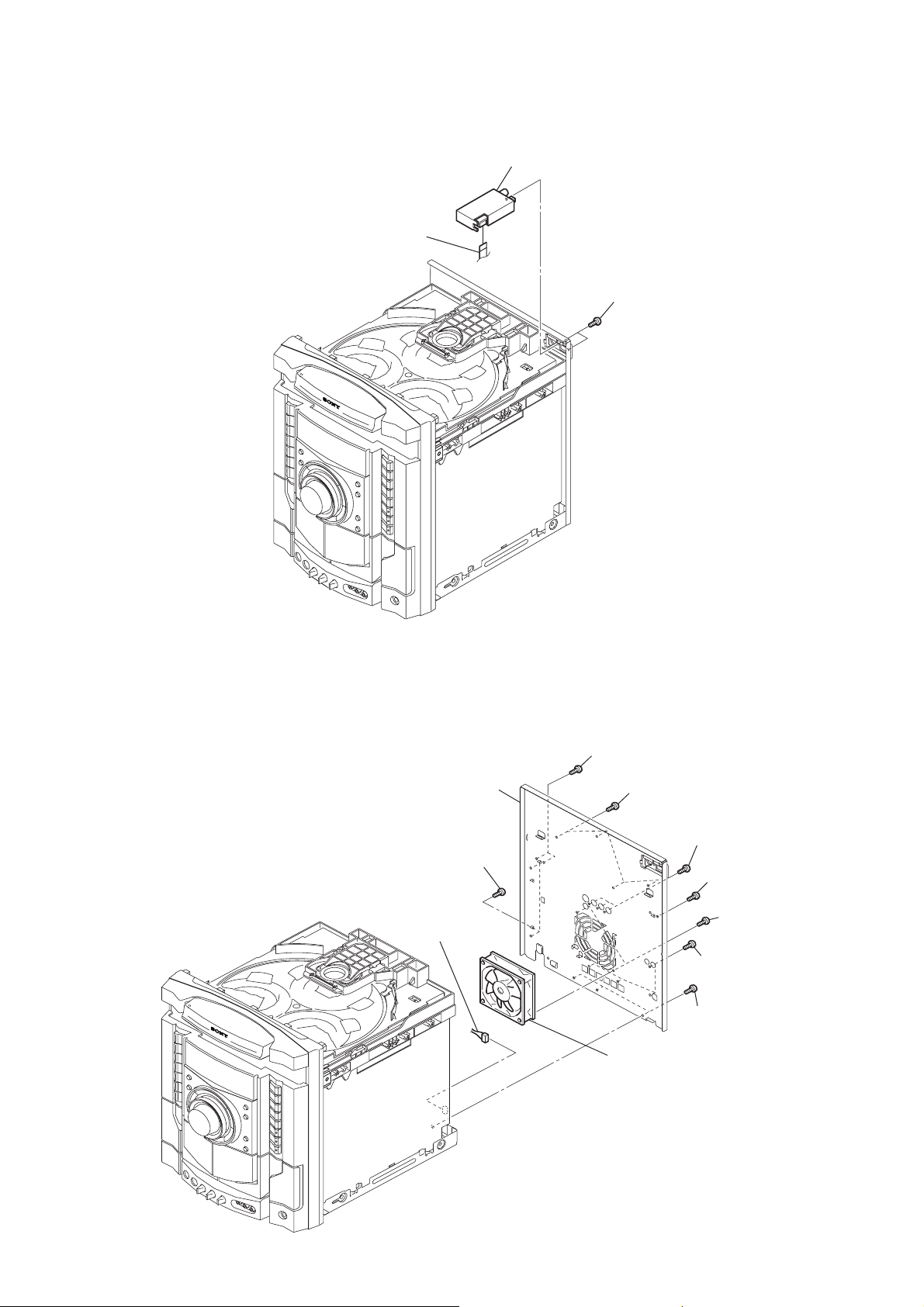
3-4. TUNER PACK
)
2
wire (flat type)
(CN1)
3
tuner pack
1
two screws
(+BVTT 3×6
HCD-GN999D
3-5. BACK PANEL, DC FAN (M891)
8
back panel
6
two screws
(+BVTP 3×8)
9
connector
(CN580)
7
two screws
(+BVTP 3
1
four screws
(+BVTP 3
qa
DC fan
(M891)
×
8)
×
2
(+BVTP 3
4
(+BVTP 3×8)
5
(+BVTP 3×8)
8)
three screws
3
screw
(+BVTP 3
0
two screws
(+BVTP 3
four screws
three screws
×
8)
×
8)
×
8)
9
Page 10
HCD-GN999D
)
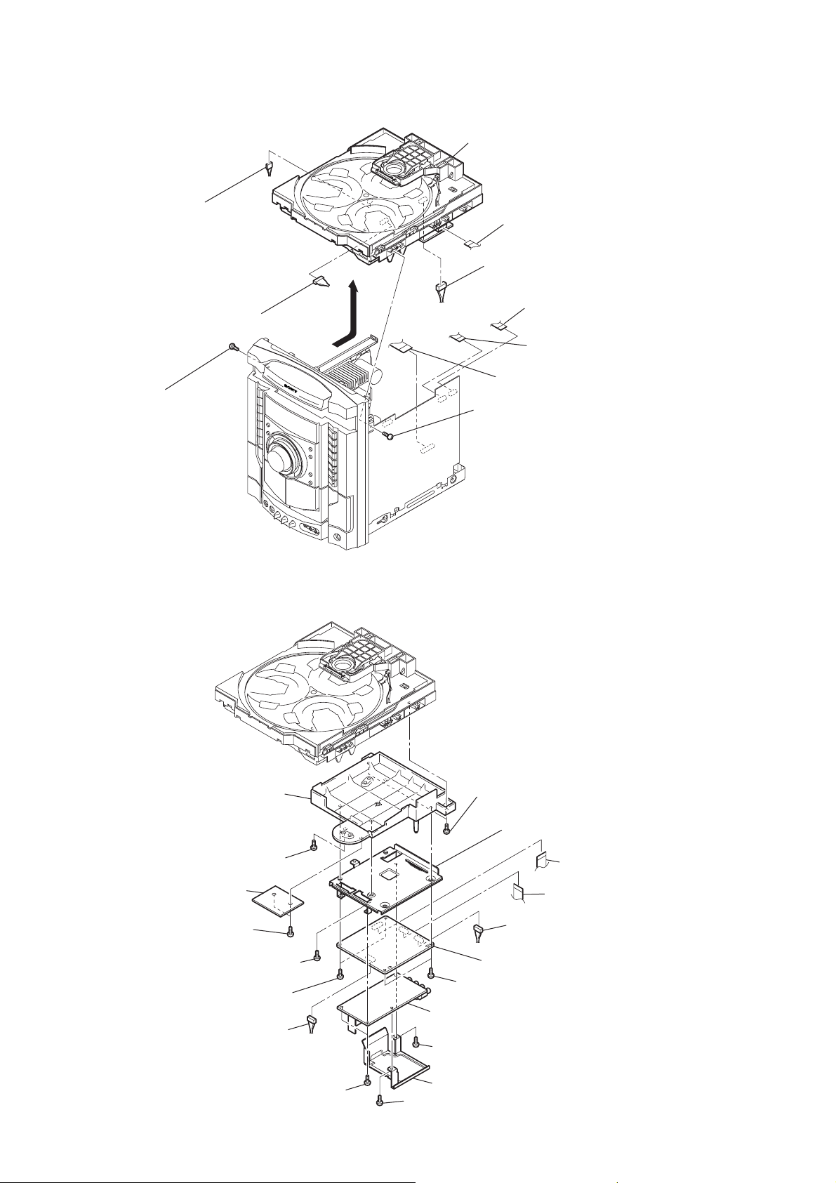
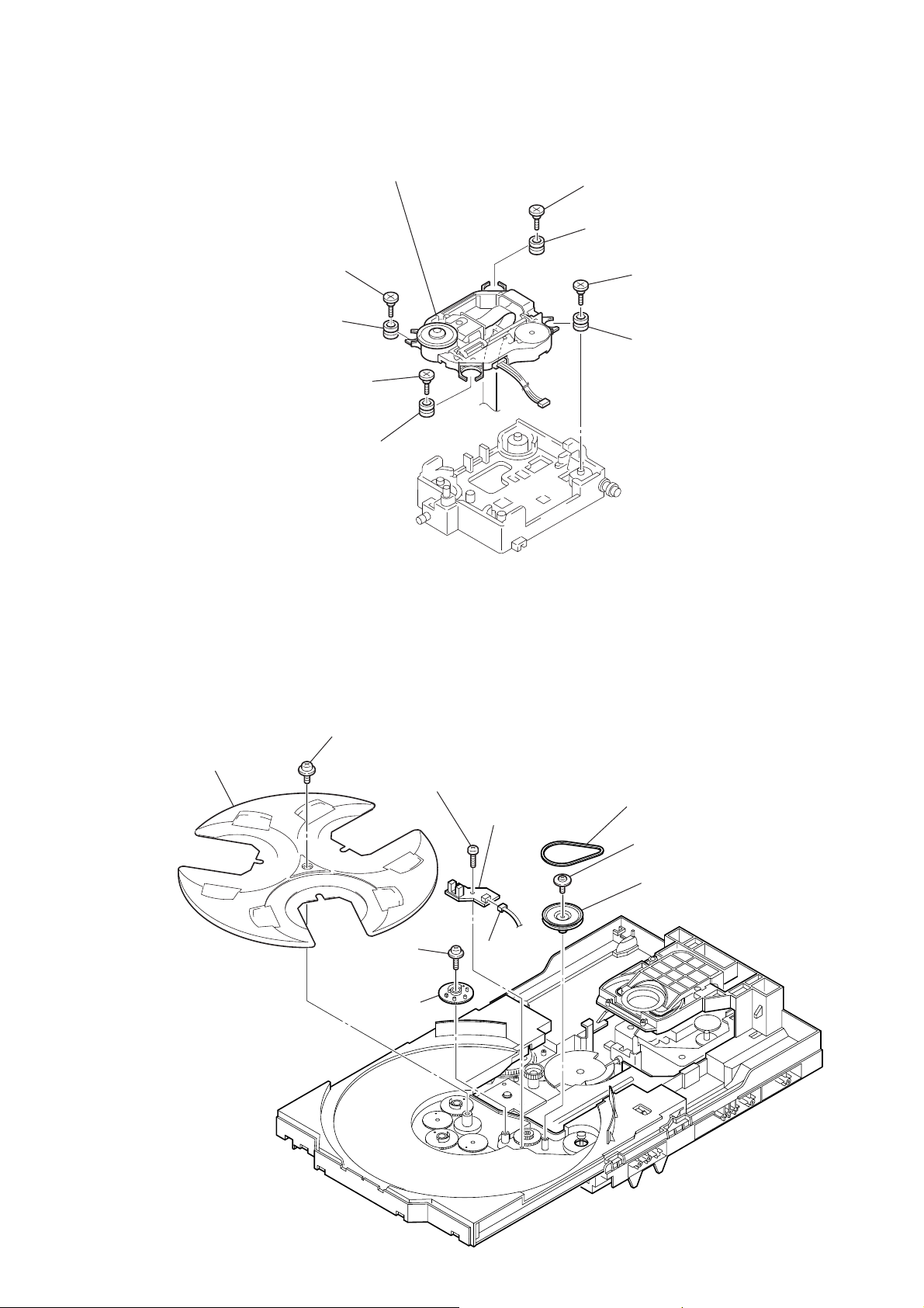
3-6. DVD MECHANISM DECK
0
connector
(CN1967)
1
tapping screw
6
connector
(CN2000)
4
qa
DVD mechanism deck
3
wire (flat type)
(CN701)
5
connector
(CN1880)
7
wire (flat type)
(CN406)
8
wire (flat type)
(CN301)
9
wire (flat type)
(CN521)
2
tapping screw
3-7. KARAOKE BOARD, VIDEO BOARD, DMB15 BOARD
ql
cover (CDM)
qj
screw
(+BVTP 3
2
KARAOKE board
1
two screws
(+BVTP 3
qg
(+BVTP 3
qd
(+BVTP 3
9
(CN401)
×
8)
×
8)
screw
two screws
connector
7
(+BVTP 3
×
8)
×
8)
two screws
×
8)
3
(+BVTP 3
qk
(+BVTP 3
qs
two screws
(+BVTP 3
8
VIDEO board
4
screw
(+BVTP 3
5
shield plate (video)
screw
×
8)
two screws
qh
bracket mediatec
0
connector
(CN401)
qf
DMB15 board
×
×
8)
×
8)
qa
(CN201)
8)
6
wire (flat type
(CN301)
wire (flat type)
10
Page 11
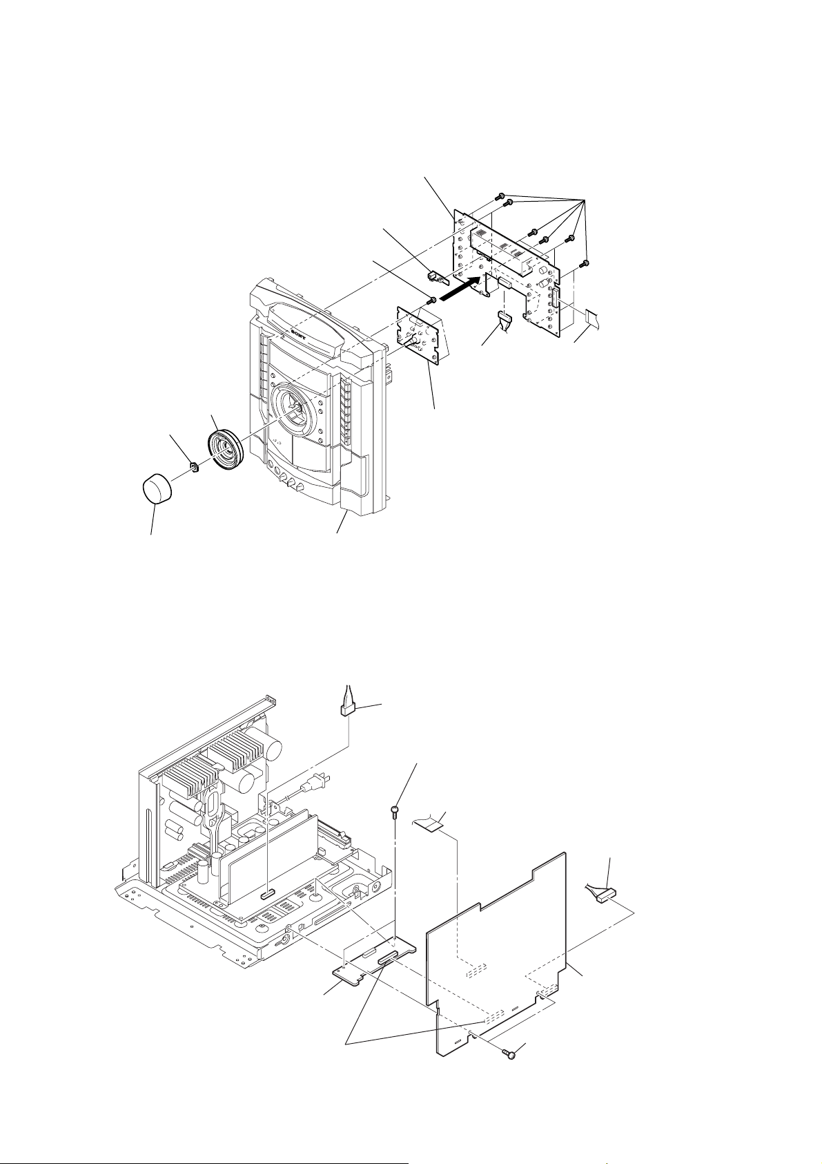
3-8. FRONT PANEL ASSY
r
8
front panel assy
6
connector
(CN121)
5
wire (flat type)
(CN101)
7
connector
(CN131)
4
wire (flat type)
(CN201)
3
connector
(CN205)
2
connecto
(CN503)
HCD-GN999D
1
four screws
(+BVTP 3
3-9. TAPE MECHANISM DECK, MIC BOARD
front panel
6
holder (TC-L)
5
holder (TC-R)
7
three
mic knobs
×
8)
2
tape mechanism deck
0
8
four screws
(+BVTP2.6)
9
(pivot)
qs
(TC)
1
(+BVTP2.6)
bracket
bracket
six screws
4
splring (L)
3
spring (R)
qa
three screws
(+BVTP3
qd
MIC board
×
8)
11
Page 12
HCD-GN999D
r
3-10. PANEL BOARD, IR BOARD, VOL BOARD
0
four screws
(+BVTP2.6)
9
knob jog assy
8
accessory nut
6
IR board
5
PANEL board
2
qa
VOL board
4
connector
(CN1452)
1
eighteen screws
(+BVTP2.6)
3
wire (flat type)
(CN1402)
7
knob (vol)
3-11. MAIN BOARD, ADC BOARD
front panel
2
connector
(CN501)
3
(+BVTT 3
two screws
1
wire (flat type)
(CN105)
×
6)
6
connecto
(CN590)
12
8
ADC board
7
board to board connector
(CN381,CN01)
4
two screws
(+BVTP 3
5
MAIN board
×
8)
Page 13
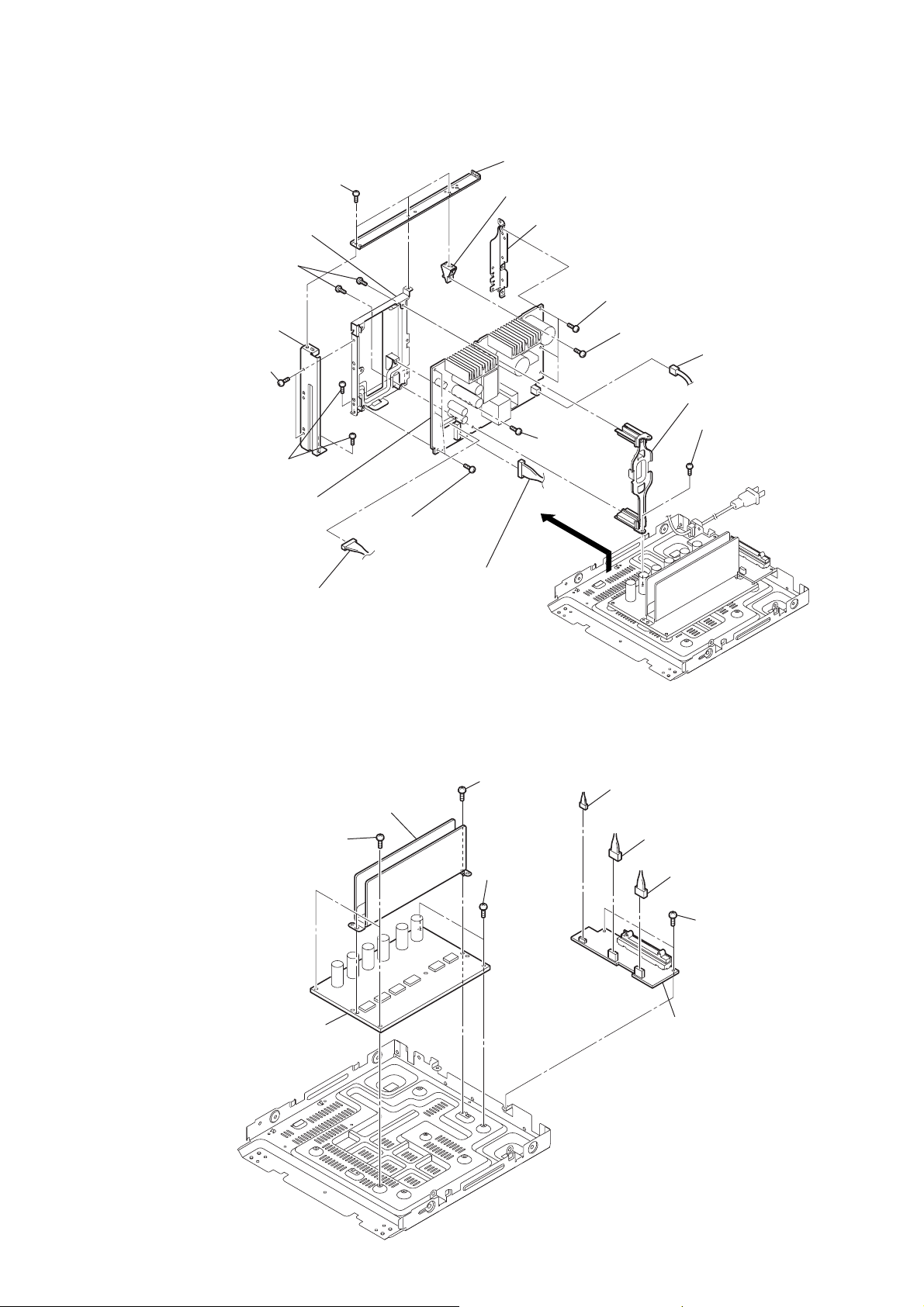
3-12. POWER BOARD
7
(+BVTP 3
qj
bracket (SMPS 5ch)
qd
two tapping screws
q;
bracket
(support front)
9
two screws
(+BVTP 3
2
(+BVTT 3
×
three screws
w;
POWER board
three screws
8)
×
6)
HCD-GN999D
8
bracket (support top)
×
8)
qh
three screws
(+BVTP 3
qs
bracket (support pwb)
ql
bracket (SMPS -B5)
qk
three screws (+BVTP 3×8)
qa
tapping screw
4
connector
(CNP1100)
qf
bracket (trans 5ch)
1
qg
screw
(+BVTP 3
×
8)
3
×
8)
screw
(+BVTT 3
×
6)
5
connector
(CN1101)
3-13. SPEAKER BOARD, SMASTER BOARD
7
heat sink (SMAS)
9
three screws
(+BVTT 3
0
SMASTER board
×
6)
6
connector
(CN1200)
6
screw
(+BVTT 3
8
two screws
(+BVTT 3
3
×
6)
×
6)
connector
(CN1700)
2
connector
(CN1700)
1
connector
(CN1700)
4
two screws
(+BVTP 3
5
SPEAKER board
×
8)
13
Page 14
HCD-GN999D
3-14. DRIVER BOARD, SW BOARD
1
two
screws
(+BTTP (M2.6))
5
DRIVER
board
3
connector (CN704)
2
wire (flat type)
(CN702)
4
connector (CN703)
6
screw
(+BTTP (M2.6))
7
SW board
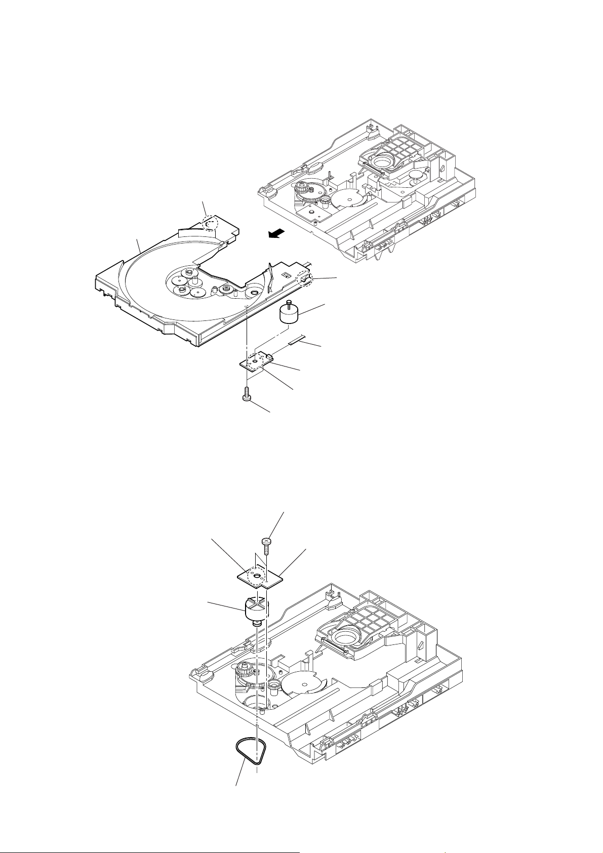
3-15. DVD ASSY
1
floating
(+PTPWH M2.6)
screw
2
DVD
assy
14
Page 15
3-16. OPTICAL PICK-UP
w
3
insulator screw
4
8
insulator
insulator screw
9
insulator
5
optical pick-up
(KHM-310CAB/C2NP)
2
insulator screw
7
insulator
1
6
HCD-GN999D
insulator scre
insulator
3-17. SENSOR BOARD
2
t
ray
1
floating
(+PTPWH M2.6)
6
floating
(+PTPWH M2.6)
7
g
screw
8
(+BTTP (M2.6))
screw
ear (geneva)
s
crew
0
SENSOR board
9
connector
(
CN731)
3
b
elt (table)
4
floating
(+PTPWH M2.6)
5
screw
p
ulley (table)
15
Page 16
HCD-GN999D
3-18. MOTOR (TB) BOARD
2
stopper
table
3-19. MOTOR (LD) BOARD
2
Remove the two solderings of motor.
4
8
6
Remove the two solderings of motor.
5
two
screws
(+BTTP (M2.6))
3
two
screws
(+BTTP (M2.6))
4
1
stopper
7
t
able motor assy (M741)
wire (flat type) (CN742)
3
MOTOR (TB) board
MOTOR (LD) board
16
5
l
oading motor assy (M751)
1
b
elt (loading)
Page 17

SECTION 4
TEST MODE
HCD-GN999D
[PANEL TEST MODE]
•This mode is used to check the fluorescent indicator tube, LEDs,
keys, VOLUME jog, model, destination, software version and
VACS level.
Procedure:
1. Press
2. All LEDs and segments in fluorescent indicator tube are lighted
3. When you want to enter to the software version dispaly mode,
4. Each time [DISC 1] button is pressed, the display changes from
5. When [DISC 3] button is pressed while the version numbers are
6. Press [DISC 2] button, the key check mode is activated.
7. In the key check mode, the fluorescent indicator tube displays
8. When [DISC 3] button is pressed after all LEDs and segments in
9. When [DISC SKIP/EX-CHANGE] button is pressed after all LEDs
10. To release from this mode, press three buttons in the same
x
button, [ILLUMINATION] button and [DISC 2] button
simultaneously.
up.
press [DISC 1] button. The model information appears on the
fluorescent indicator tube. Press [DISC 1] button again to view
the destination information.
MC version, SYS version, UI version, DVD version, CDMA
version, CDMB version, ST version, TA version, TM version,
TC version in this order, and returns to the model version display.
being displayed except model and destination, the date of the
software creation appears. When [DISC 3] button is pressed
again, the display returns to the software version display. When
[DISC 1] button is pressed while the date of the software creation
is being displayed, the date of the software creation is displayed
in the same order of software version display.
“K 0 V0”.
Turn the [OPERATION DIAL] clockwise; “K” value increases by
one. Turn the [OPERATION DIAL] counterclockwise; “K” value
decreases by one. Each time a button is pressed, “K” value
increases. Press other keys on main unit to check whether the
key is detected. However, once a button has been pressed, it is
no longer taken into account.
“V” value increases in the manner of 0, 1, 2, 3 ... if [VOLUME]
knob is turned clockwise, or it decreases in the manner of 0, 9,
8, 7 ... if [VOLUME] knob is turned counterclockwise.
fluorescent indicator tube light up, the fluorescent indicator tube
displays “VACS A”. A is VACS level which is triggered by signal
level.
and segments in fluorescent indicator tube light up, alternate
segments in fluorescent indicator tube would light up. If you
press [DISC SKIP/EX-CHANGE] button again, another half of
alternate segments in fluorescent indicator tube would light up.
When [DISC SKIP/EX-CHANGE] button is pressed again, all
segments lights off. Press [DISC SKIP/EX-CHANGE] button again
would cause all segments lights up.
manner as step 1, or disconnect the power cord.
• Check of Amplifier
1. Press [EQ BAND/MEMORY] button repeatedly until a message
“GEQ MAX” appears on the fluorescent indicator tube. GEQ
increases to its maximum.
2. Press [EQ BAND/MEMORY] button repeatedly until a message
“GEQ MIN” appears on the fluorescent indicator tube. GEQ
decreases to its minimum.
3. Press [EQ BAND/MEMORY] button repeatedly until a message
“GEQ FLAT” appears on the fluorescent indicator tube. GEQ
is set to flat.
4. When the [VOLUME] knob is turned clockwise even slightly,
the sound volume increases to its maximum and a message
“VOLUME MAX” appears on the fluorescent indicator tube.
5. When the [VOLUME] knob is turned counterclockwise even
slightly, the sound volume decreases to its minimum and a
message “VOLUME MIN” appears on the fluorescent indicator
tube.
•Tape function
1. When a tape is inserted in Deck B and recording is started, the
function is changed to TV automatically. When [CD SYNC] button
is pressed during recording in function, ALC (Automatic Level
Control) is turned on.
2. During recording, press
and the function is changed to TAPE B and rewind the tape in
Deck B until the recording start position and playback of the
tape in Deck B is started. If the [REC PAUSE/START] button is
pressed for a pause and pressed again to resume recording during
recording time, when the tape is rewind, the tape will be rewind
until the position where the pause is applied.
•To release from Common Test mode
1. To release from this mode, press
2. The cold reset is enforced at the same time.
[COLD RESET]
• The cold reset clears all data including preset data stored in the
RAM to initial conditions. Execute this mode when returning
the set to the customer.
Procedure:
1. Press
2. Press
3. The message “COLD RESET” appears on the fluorescent
[VACS ON/OFF]
• This mode is used to switch on and off the VACS (Variable
^/1
button to turn on the system.
button, [ILLUMINATION] button, and
x
simultaneously.
indicator tube. Then, the fluorescent indicator tube becomes
blank for a while, and the system is reset.
Attenuation Control System).
button will stop the recording
m
^/1
button.
^/1
button
[COMMON TEST MODE]
• This mode is used to check operations of the respective sections
of Amplifier and Tape.
Procedure:
•To enter Common Test Mode
1. Press
2. The DVD ring indicators and the line below DVD ring indicator
x
button, [ILLUMINATION] button and [DISC 3] button
simultaneously.
flash synchronously on the fluorescent indicator tube. The
function is changed to TV where the function is changed to
DVD.
Procedure:
1. Press
2. Press
[TUNER STEP CHANGE]
• The step interval of AM channels can be toggled between 9 kHz
^/1
button to turn on the system.
button, [DIRECTION] button and [DISC 1]
x
simultaneously. The message “VACS OFF” or “VACS ON”
appears on the fluorescent indicator tube.
and 10 kHz. This mode is not available for Saudi Arabia and
Russia models.
17
Page 18

HCD-GN999D
Procedure:
1. Press ?/1 button to turn on the system.
2. Press [TUNER/BAND] button repeatedly to select the “AM”.
3. Press ?/1 button to turn off the system.
4. Press [ILLUMINATION] button and ?/1 button simultaneously.
The system will turn on automatically. The message “AM 9K
STEP” or “AM 10K STEP” appears on the fluorescent indicator
tube and thus the channel step is changed.
[DVD SHIP MODE (WITH MEMORY CLEAR)]
• This mode moves the optical pick-up to the position durable to
vibration and clears all data including preset data stored in the
RAM to initial conditions. Use this mode when returning the
set to the customer after repair.
Procedure:
1. Press ?/1 button to turn on the system.
2. Select DVD function.
3. Press x button, [DIRECTION] button and ?/1 button
simultaneously during “DVD NO DISC” condition. The system
will turn off automatically.
4. After the “STANDBY” blinking display finishes, a message
“MECHA LOCK” appears on the fluorescent indicator tube and
the DVD ship mode is set.
[DVD SHIP MODE (WITHOUT MEMORY CLEAR)]
• This mode moves the optical pick-up to the position durable to
vibration. Use this mode when returning the set to the customer
after repair.
Procedure:
1. Press ?/1 button to turn on the system.
2. Select DVD function.
3. Press [DVD] button and ?/1 button simultaneously during “DVD
NO DISC” condition. The system will turn off automatically.
4. After the “STANDBY” blinking display finishes, a message
“MECHA LOCK” appears on the fluorescent indicator tube and
the DVD ship mode is set.
[DVD TRAY LOCK MODE]
• This mode let you lock the disc tray. When this mode is
activated, the disc tray will not open when [OPEN/CLOSE]
button or [DISC SKIP/EX-CHANGE] button is pressed. The
message “LOCKED” will appears on the fluorescent indicator
tube.
Procedure:
1. Press ?/1 button to turn on the system.
2. Select DVD function.
3. Press x button and [OPEN/CLOSE] button simultaneously and
hold down until “LOCKED” or “UNLOCKED” appears on the
fluorescent indicator tube (around 5 seconds).
[TCM OFFLINE MODE]
• This mode prevents the system from turning off automatically
when TCM is not connected. Therefore, measurements can be
done even when TCM is not connected during production.
Procedure:
1. When the system is turned off, press [EQ BAND/MEMORY]
button, [TAPE A/B] button and ?/1 button simultaneously. The
system will turn on automatically.
2. The message “TCM OFFLINE” will appears on the fluorescent
indicator tube.
•To release from TCM Offline Mode
To release from this mode, perform “COLD RESET” or turn off
the power supply.
[TV/SAT SWITCHING]
• This mode let you switch from TV to SAT and vice-versa.
Procedure:
1. Press ?/1 button to turn on the system.
2. Select TV function.
3. Press [TV/SAT] button and ?/1 button simultaneously. The
function will change to SAT. Press the same buttons again to
change from SAT to TV.
[DVD COLOR SYSTEM]
• This mode let you change the color system of the video output
from PAL to NTSC or vice-versa. This mode is not available for
Latin American and Russian models.
Procedure:
1. Press ?/1 button to turn on the system.
2. Select DVD function.
3. Press ?/1 button again to turn off the system.
4. Press X button and ?/1 button simultaneously. The system
will turn on automatically.
The message “COLOR PAL” or “COLOR NTSC” appears on
the fluorescent indicator tube.
[REMOTE DISABLE MODE]
• This mode let you disable the remote commander reception.
When this mode is activated, the system will not response if the
button on the remote commander is pressed. The message “RM
DISABLE” appears on the fluorescent indicator tube.
This mode is essential for conducting test and repairing when
no interruption from the other remote commander is expected.
This mode is cancelled automatically when the system is turned
off.
Procedure:
1. Press ?/1 button to turn on the system.
2. Press x button, [DIRECTION] button and [DISC 3] button
simultaneously until “SIRCS ON” or “SIRCS OFF” appears on
the fluorescent indicator tube.
[PROGRESSIVE]
• This mode let you change the format of the video output from
the COMPONENT OUT jacks among PROGRESSIVE AUTO,
PROGRESSIVE VIDEO and INTERLACE.
Procedure:
1. Press ?/1 button to turn on the system.
2. Press [DVD] button and [DISPLAY] button simultaneously. “P
AUTO” or “P VIDEO” or “INTERLACE” appears on the
fluorescent indicator tube.
[MTK FIRMWARE DISPLAY]
• This mode is used to display the MTK firmware version.
Procedure:
1. Press ?/1 button to turn on the system.
2. Press [DVD] button to switch to DVD function.
3. Press ?/1 button again to turn off the system.
4. Press x button and ?/1 button. The system turns on
automatically.
5. The version of MTK firmware appears on the TV screen.
[DVD SERVICE MODE]
• This mode let you make diagnosis and adjustment easily by
using the remote commander and the TV. The instructions,
diagnostic results, etc. are given on the on-screen display.
18
Page 19
HCD-GN999D
[DVD SERVICE MODE]
•This mode let you make diagnosis and adjustment easily by
using the remote commander and the TV. The instructions,
diagnostic results, etc. are given on the on-screen display.
• TEST DISC LIST
Be sure to use the DVD disc that matches the signal standards of
your region.
• CD
YEDS-18 (Part No.: 3-702-101-01)
PATD-012 (Part No.: 4-225-203-01)
• DVD SL (Single Layer)
NTSC : HLX-503 (Part No.: J-6090-069-A)
HLX-504 (Part No.: J-6090-088-A)
PA L:HLX-506 (Part No.: J-6090-077-A)
• DVD DL (Dual Layer)
NTSC : HLX-501 (Part No.: J-6090-071-A)
HLX-505 (Part No.: J-6090-089-A)
PA L:HLX-507 (Part No.: J-6090-078-A)
• Procedure to enter to DVD Service Mode:
^/1
1. Press
button to turn on the system.
2. Select DVD function.
3. Press
button and [OPEN/CLOSE] button simultaneously and
x
then turn the [VOLUME] knob clockwise.
4. The message “SERVICE IN” appears on the fluorescent
indicator tube and the Top Menu of Remocon Diagnosis Menu
appears on the on-screen display on the TV. The model name
and revision number is displayed at the bottom of the on-screen
display.
Remocon Diagnosis Menu
0. External Chip Check
1. Servo Parameter Check
2. Drive Manual Operation
3. Emergency History
4. Version Information
Model Name : GML6DS_ME
IF-con : V
Syscon : Ver.
er. 01.00 (0000)
0.302
5. To execute each function, press its number by using numeric
button on the remote commander.
6. To release from this mode, press
^/1
button to turn off the
system.
• Execute IOP Measurement
In order to execute mirror time adjustment, the following
standard procedures must be followed.
1. From the Top Menu of Remocon Diagnosis Menu, select “2.
Drive Manual Operation” by pressing the [2] button on the
remote commander. The following screen appears on the onscreen display.
Drive Manual Operation
1. Servo Control
2. Track/Layer Jump
3. Manual Adjustment
4. Mecha test Mode
5. MIRR time Adjust
0. Return to Top Menu
2. Select “3. Manual Adjustment” by pressing the [3] button on
the remote commander. The following screen appears on the
on-screen display.
Manual Adjust
1. Track Balance Adjust:
2. Track Gain Adjust:
3. Focus Balance Adjust:
4. Focus Gain Adjust:
5. Eg Boost Adjust:
6. Iop:
7. TRV. Level:
8. S curve(FE) Level:
9. RFL(PI) Level:
0. MIRR Time:
O o Change Value
RETURN Return to previous menu
3. Select “6. Iop:” by pressing [6] button on the remote commander.
4. Wait until a hexadecimal number appears in the on-screen
display as below:
Manual Adjust
1. Track Balance Adjust:
2. Track Gain Adjust:
3. Focus Balance Adjust:
4. Focus Gain Adjust:
5. Eg Boost Adjust:
6. Iop. ED:
7. TRV. Level:
8. S curve(FE) Level:
9. RFL(PI) Level:
0. MIRR Time:
O o Change Value
RETURN Return to previous menu
5. Convert data from hexadecimal to decimal by using conversion
table.
6. Press [RETURN] button on the remote commander to return to
previous menu.
7. Press [0] button on the remote commander to return to the Top
Menu of Remocon Diagnosis Menu.
8. Press
^/1
button to turn off the system.
• Check Emergency History
To check the emergency history, please follow the following
procedure.
1. From the Top Menu of Remocon Diagnosis Menu, select “3.
Emergency History” by pressing the [3] button on the remote
commander. The following screen appears on the on-screen
display.
Emg.History Check
Laser Hours CD 999h 59min
1. 01 05 04 04
00 00 00 00 00 00 23 45
2. 02 02 01 01 00 A9 4B 00
00 00 00 00 00 00 23 45
Next Next Page Prev Prev Page
O Return to Top Menu
DVD 999h 59min
00 92 46 00
19
Page 20
HCD-GN999D
2. You can check the total time when the laser is turned on during
playback of DVD and CD from the above menu. The maximum
time, which can be displayed are 999h 59min.
3. You can check the error code of latest 10 emergency history
from the above menu. To view the previous or next page of
emergency history, press . or > on the remote
commander. The error code consists of
• Error Code
Example of Error code
1. 01 05 04 04 00 92 46 00
00 00 00 00 00 00 23 45
The meaning of error code is as below:
01: Communication error (No reply from syscon)
02: Syscon hung up
03: Power OFF request when syscon hung up
19: Thermal shutdown
24: MoveSledHome error
25: Mechanical move error (5 Changer)
26: Mechanical move stack error
30: DC motor adjustment error
31: DPD offset adjustment error
32: TE balance adjustment error
33: TE sensor adjustment error
34: TE loop gain adjustment error
35: FE loop gain adjustment error
36: Bad jitter after adjustment
40: Focus NG
42: Focus layer jump NG
52: Open kick spindle error
51: Spindle stop error
60: Focus on error
61: Seek fail error
62: Read Q data/ID error
70: Lead in data read fail
71: TOC read time out (CD)
80: Can’t buffering
81: Unknown media type
• Parameter of error code
This is the detail of error code.
To clear the Laser Hour
Press [DISPLAY] button and then press [CLEAR] button. The data
for both CD and DVD data are reset.
Emg.History Check
Laser Hours CD 0h 0min
1. 01 05 04 04
00 00 00 00 00 00 23 45
2. 02 02 01 01 00 A9 4B 00
00 00 00 00 00 00 23 45
Next Next Page Prev Prev Page
O Return to Top Menu
DVD 0h 0min
00 92 46 00
To clear the Emergency History
Press [MENU] button and then press [CLEAR] button. The error code
for all emergency history would be reset.
Emg.History Check
Laser Hours CD 999h 59min
1. 00 00 00 00
00 00 00 00 00 00 00 00
2. 00 00 00 00 00 00 00 00
00 00 00 00 00 00 00 00
Next Next Page Prev Prev Page
O Return to Top Menu
DVD 999h 59min
00 00 00 00
To return to the Top Menu of Remocon Diagnosis Menu
Press [0] button on the remote commander.
• Check Version Information
To check the version information, please follow the following
procedure.
1. From the Top Menu of Remocon Diagnosis Menu, select “4.
Version Information” by pressing the [4] button on the remote
commander. The following screen appears on the on-screen
display.
Example of Error code
1. 01 05 04 04 00 92 46 00
00 00 00 00 00 00 23 45
•Time of error code
This is the laser time when an error occurred.
Example of Error code
1. 01 05 04 04 00 92 46 00
00 00 00 00 00 00 23 45
20
Version information
Firm (Main) : Ver. xxxxx
Firm (Sub) : xxxxx
RISC : xxxxx
8032 : xxxxx
Audio DSP : xxxxx
Servo DSP : xxxxx
O Return to Top Menu
To return to the Top Menu of Remocon Diagnosis Menu, press
[0] on the remote commander.
Page 21

SECTION 5
MECHANICAL ADJUSTMENTS
Precaution
1. Clean the following parts with a denatured alcohol-moistened
swab:
record/playback heads pinch rollers
erase head rubber belts
capstan idlers
2. Demagnetize the record/playback head with a head
demagnetizer.
3. Do not use a magnetized screwdriver for the adjustments.
4. After the adjustments, apply suitable locking compound to the
parts adjusted.
5. The adjustments should be performed with the rated power
supply voltage unless otherwise noted.
Torque Measurement
Mode Torque meter Meter reading
2.9m N • m to 6.9m N • m
FWD CQ-102C 30 to 70 g • cm
(0.42 – 0.97 oz • inch)
FWD
back tension
REV CQ-102RC 30 to 70 g • cm
REV
back tension
FF/REW CQ-201B 49 to 170 g • cm
CQ-102C 2 to 6 g • cm
CQ-102RC 2 to 6 g • cm
0.15m N • m to 0.59m N • m
(0.03 – 0.08 oz • inch)
2.9m N • m to 6.9m N • m
(0.42 – 0.97 oz • inch)
0.15m N • m to 0.59m N • m
(0.03 – 0.08 oz • inch)
4.8m N • m to 16.7m N • m
(0.68 – 2.36 oz • inch)
HCD-GN999D
21
Page 22
HCD-GN999D
)
SECTION 6
ELECTRICAL ADJUSTMENTS
DVD SECTION
When the base unit is replaced, perform the adjustment and the
measurement as shown below in this order.
1) MIRROR TIME ADJUSTMENT
2) EXECUTING IOP MEASUREMENT (See page 19)
[TEST DISC LIST]
Be sure to use the DVD disc that matches the signal standards of
your region.
• CD
YEDS-18 (Part No.: 3-702-101-01)
PATD-012 (Part No.: 4-225-203-01)
• DVD SL (Single Layer)
NTSC : HLX-503 (Part No.: J-6090-069-A)
HLX-504 (Part No.: J-6090-088-A)
PAL : HLX-506 (Part No.: J-6090-077-A)
• DVD DL (Dual Layer)
NTSC : HLX-501 (Part No.: J-6090-071-A)
HLX-505 (Part No.: J-6090-089-A)
PAL : HLX-507 (Part No.: J-6090-078-A)
[RFMON Level Check]
Connection:
oscilloscope
DMB15 board
CN105 pin 6 (RFMON)
CN105 pin
3
(GND)
+
–
Checking Location: DMB15 board (Side A)
IC102
(SIDE A)
IC104
CN105
IC201
6
1
CN105 pin 3 (GND
DMB15 BOARD
IC101
CN106
CN105 pin 6 (RFMON)
VIDEO SECTION
Video Level Check (VIDEO BOARD)
Purpose
This adjustment is made to satisfy the NTSC standard, and if not
adjusted correctly, the brightness will be too large or small.
Procedure:
1. Connect an oscilloscope to CN105 pin 6 (RFMON) and
CN105 pin 3 (GND) on the DMB15 board.
2. Turn the power on.
3. Set the test disc (refer to the TEST DISC LIST) on the tray
and press H button to playback.
4. Confirm that oscilloscope waveform is clear and check
RFMON signal level is correct or not.
Note: A clear RFMON signal waveform means that the shape “◊” can be
clearly distinguished at the center of the waveform.
RFMON signal waveform
VOLT/DIV: 200 mV
TIME/DIV: 500 ns
level: 0.58 ± 1.23 Vp-p (DVD)
0.57 ± 1.1 Vp-p (CD)
oscilloscope
Ω
75
set
J1902
VIDEO OUTPUT
Procedure:
1. Connect oscilloscope to VIDEO output.
2. Load a DVD reference disc playback.
3. Check the video signal level is 1.00±0.07Vp-p.
(WHITE 100%)
1.00 ± 0.07 Vp-p
22
Page 23
HCD-GN999D
r
e
DECK SECTION
0 dB=0.775 V
1. Demagnetize the record/playback head with a head
demagnetizer.
2. Do not use a magnetized screwdriver for the adjustments.
3. After the adjustments, apply suitable locking compound to the
parts adjust.
4. The adjustments should be performed with the rated power
supply voltage unless otherwise noted.
5. The adjustments should be performed in the order given in this
service manual. (As a general rule, playback circuit adjustment
should be completed before performing recording circuit
adjustment.)
6. The adjustments should be performed for both L-CH and RCH.
7. Switches and controls should be set as follows unless otherwise
specified.
•Test Tape
Tape Signal Used for
P-4-A063 6.3 kHz, –10 dB Azimuth Adjustment
Record/Playback Head Azimuth Adjustment
DECK A DECK B
Note: Perform this adjustments for both decks
Procedure:
1. Mode: Playback
3. Mode: Playback
pin 1
L
R
pin 2
good
MAIN
board
CN111
pin 3
oscilloscop
V
wrong
H
°
test tape
P-4-A063
(6.3 kHz, –10 dB)
L-CH
set
R-CH
waveform of oscilloscope
in phase 45°90°135°180
4. After the adjustments, apply suitable locking compound to the
pats adjusted.
Adjustment Location: Playback Head (Deck A).
Record/Playback/Erase Head (Deck B).
test tape
P-4-A063
(6.3 kHz, –10 dB)
set
MAIN board
CN111
Pin 1 (L-CH)
Pin 3 (R-CH)
MAIN board
CN111
Pin 2 (GND)
level mete
+
–
2. Turn the adjustment screw and check output peaks. If the peaks
do not match for L-CH and R-CH, turn the adjustment screw
so that outputs match within 1dB of peak.
output
level
within
1dB
L-CH
peak
R-CH
peak
within
1dB
screw
position
L-CH
peak
screw
position
R-CH
peak
forward
reverse
23
Page 24

HCD-GN999D
MEMO
24
Page 25
SECTION 7
d
DIAGRAMS
HCD-GN999D
For Schematic Diagrams.
Note:
• All capacitors are in µF unless otherwise noted. (p: pF)
50 V or less are not indicated except for electrolytics and
tantalums.
• All resistors are in Ω and 1/
specified.
•%: indicates tolerance.
• f : internal component.
• 2 : nonflammable resistor.
• 5 : fusible resistor.
Note:
The components identified by mark 0 or dotted line
with mark 0 are critical for safety.
Replace only with part number specified.
• C : panel designation.
• A : B+ Line.
• B : B– Line.
•Voltages and waveforms are dc with respect to ground under no-signal (detuned) conditions.
DMB15 and VIDEO boards
no mark : DVD PLAY
Other board
no mark : TUNER (FM/AM)
( ) : DVD PLAY
< > : TAPE PLAY
[ ] : TAPE REC
* : Impossible to measure
•Voltages are taken with a VOM (Input impedance 10 MΩ).
Voltage variations may be noted due to normal production
tolerances.
•Waveforms are taken with a oscilloscope.
Voltage variations may be noted due to normal production
tolerances.
• Circled numbers refer to waveforms.
• Signal path.
F : AUDIO
e : TUNER
k : TAPE PLAY (DECK A)
d : TAPE PLAY (DECK B)
G : REC (DECK B)
J : DIGITAL
N : MIC
c : DVD/CD (RF)
L : VIDEO
E : Y
a : CHROMA
r : COMPONENT VIDEO
q : R, G, B
4
W or less unless otherwise
Note on Printed Wiring Boards.
Note:
• X : parts extracted from the component side.
• : Pattern from the side which enables seeing.
(The other layers' patterns are not indicated.)
Caution:
Pattern face side: Parts on the pattern face side seen from
(SIDE A) the pattern face are indicated.
Parts face side: Parts on the parts face side seen from
(SIDE B) the parts face are indicated.
• Indication of transistor.
C
Q
B
E
Q
B
CE
Q
B
CE
• Abbreviation
E2 : 120V AC Area in E model
E3 : 240V AC Area in E model
E12 : 220V-240V AC Area in E model
E13 : 220-230V AC area in E model
E15 : Iran model
E51 : Chilean and Perurian model
EA : Saudi Arabia model
MX : Mexican model
MY : Malaysia model
PH : Philippines model
SP : Singapore model
TH : Thai model
These are omitted.
These are omitted.
These are omitted.
• Circuit Boards Location
MOTOR (LD) board
KARAOKE board
POWER board
PANEL board
IR board
VOL board
MIC board
SENSOR board
SW board
DMB15 board
VIDEO board
TUNER pack
DRIVER board
MOTOR (TB) board
SPEAKER board
MAIN board
SMASTER boar
ADC board
NOTE ON REPLACEMENT OF DMB15 BOARD
New part of EEPROM (IC103) on the DMB15 board cannot be used. Therefore, if
the mounted DMB15 board (A-1167-802-A or A-1167-915-A or A-1188-872-A) is
replaced, exchange new EEPROM with that used before the replacement.
HCD-GN999D
2525
Page 26
HCD-GN999D
1.0 Vp-p
H
0.5 V/DIV, 20 µsec/DIV
1.3 Vp-p
H
0.5 V/DIV, 20 µsec/DIV
1.6 Vp-p
H
0.5 V/DIV, 20 µsec/DIV
1.6 Vp-p
H
0.5 V/DIV, 20 µsec/DIV
0.8 Vp-p
H
0.5 V/DIV, 20 µsec/DIV
2.0 Vp-p
H
1 V/DIV, 20 µsec/DIV
2.6 Vp-p
H
1 V/DIV, 20 µsec/DIV
1 V/DIV, 20
µ
sec/DIV
0.8 Vp-p
H
0.5 V/DIV, 20 µsec/DIV
1.5 Vp-p
H
1 V/DIV, 20 µsec/DIV
1 V/DIV, 20
µ
sec/DIV
2.0 Vp-p
H
1 V/DIV, 20 µsec/DIV
1 V/DIV, 20
µ
sec/DIV
2.0 Vp-p
H
1.5 Vp-p
H
2.6 Vp-p
H
1
IC1801 2
CIN
2
IC1801 4
CVBSIN
3
IC1801 6
YIN
qa
IC1801 wd
CVBSOUT
qs
IC1801 wh
C OUT
qd
IC1805 7
VOUT
4
IC1801 0
CYIN
5
IC1801 qs
CBIN
6
IC1801 qf
CRIN
7
IC1801 qh
CROUT
8
IC1801 qk
CBOUT
9
IC1801 w;
CYOUT
0
IC1801 wa
YOUT
•Waveforms
– DMB15 Board –
1
2V/DIV, 0.1 msec/DIV
2
2V/DIV, 20 nsec/DIV
3
IC301 9
IC301 0
41 nsec
IC102 6
BICK
0.33
m
sec
MCLK
DVDRFIP
3.3 Vp-p
4.0 Vp-p
4
0.1V/DIV, 0.5 msec/DIV
5
0.1 V/DIV, 0.5 msec/DIV
6
IC102 ea
IC102 es
IC102
XTALO
228
FED
TEO
0.1 Vp-p
0.1 Vp-p
– MAIN Board –
1
IC401 qa
1V/DIV, 10 µsec/DIV
2
IC401 qd
1V/DIV, 1
3
T101 5
XC-OUT
30.5
µsec
X-OUT
2 µsec
µ
sec/DIV
TAPE REC only
– VIDEO Board –
2.7 Vp-p
3.3 Vp-p
– SMASTER Board –
0.2V/DIV, 50 nsec/DIV
1
IC800 2
0.5V/DIV, 20 nsec/DIV
20.3 nsec
0.6 Vp-p
0.8 Vp-p
40 nsec
0.5V/DIV, 20 nsec/DIV
1.1 Vp-p
10.5 µsec
50V/DIV, 10 µsec/DIV
4
T101 4
50V/DIV, 10
TAPE REC only
10.5 µsec
µ
sec/DIV
67 Vp-p
82 Vp-p
– ADC Board –
1
IC03 1
HCD-GN999D
2V/DIV, 50 nsec/DIV
81.3 nsec
4 Vp-p
2626
Page 27
7-1. BLOCK DIAGRAM – RF SECTION –
RF
A
CD LD
PD
DVD LD
WR650
VR780
B
C
D
F
E
VC
Q102 (1/2)
AUTOMATIC POWER
CONTROL (FOR CD)
Q102 (2/2)
AUTOMATIC POWER
CONTROL (FOR DVD)
Q101
Q103
DETECTOR
OPTICAL PICK-UP
BLOCK
(KHM-310CAB)
LASER
DIODE
(FOR CD)
LASER
DIODE
(FOR DVD)
6
2
3
4
5
19
18
8
9
10
11
29
23
20
21
22
50
DVDRFIP
DVDA
DVDB
DVDC
DVDD
TPI
TNI
NA
NB
MC
MD
V2O
LD01
MDI2
MDI1
LD02
MSW
OSP
252 253
OSN
IC102 (1/2)
CD/DVD RF AMP,
FOCUS/TRACKING ERROR AMP
DVD SYSTEM PROCESSOR
DIGITAL SERVO PROCESSOR
ASDATA0
ASDATA1
ASDATA2
ASDATQ3
ACLK
ABCK
ALRCK
XRST
SDA
SCL
VOICE/YUV7
SMSCK
217
218
219
222
215
214
213
220
103
102
206
208
14
SDTI1
15
SDTI2
16
SDTI3
13
SDTI4
10
MCLK
9
BICK
17
LRCK
8
PDN
CONVERTER
20
SDA
19
CSL
SDA
5
SCL
6
IC301
D/A
IC103
EEPROM
LOUT4+
LOUT4-
ROUT4+
ROUT4-
LOUT1+
LOUT1ROUT1+
ROUT1-
LOUT3+
LOUT3-
ROUT3+
ROUT3-
LOUT2+
LOUT2-
ROUT2+
ROUT2-
IC3771
38
37
33
32
3
2
5
6
IC3711
2
1
48
47
3
2
5
6
IC3751
42
41
40
39
3
2
5
6
IC3731
46
45
44
43
(IC3711,3731,3751,3771)
3
2
5
6
BIAS
XVOICE
SCORE
AMP
AMP
AMP
AMP
Q3801
BIAS
B
1
7
1
7
1
7
1
7
MAIN
SECTION
(Page 30)
HCD-GN999D
LT
RT
FL
FR
MAIN
SECTION
A
(Page 30)
FC
SW(LEE)
SL
SR
AU+5V
2AXIS
DEVICE
FOCUS/
TRACKING
COIL
MSW
FCS+
FCS–
TRK+
TRK–
(SLED)
M1
(SPINDLE)
S1
(LIMIT)
M2
MM
MM
REG02
SP+
SP–
FOCUS/TRACKING COIL DRIVER,
IC201
SPINDLE, SLED MOTOR DRIVER
42
NC
41
NC
36 48
37 1
35 3
34 4
REG01
32
31
SL–
30
SL+
29
27
28
46
47
BUFFER
FOCUS COIL
DRIVE
TRACKING COIL
DRIVE
SLED MOTOR
DRIVE
SLED MOTOR
DRIVE
SPINDLE MOTOR
DRIVE
BUFFER
9
12
43
10
13
42
40
21
19
20
22
45
VREFO
FOO
TRO
FMO
DMO
IOP
IOPMON
VREFO
FMO
FOO
DMO
TRO
30
38
42
37
41
245
246
40
211
210
170
47
176
VREFO
FMO
FOO
DND
TRO
RFRPDC
RFRPAC
IOPMON
MUTE123
MUTE
TSD M
SPFG
LIMSW
TXD
RXD
V2 REF0
PRST
IFCK
IFSDO
IFSDI
XIFCS
IFBSY
MIC/VSYNC
KRMOD/HSYNC
107
106
28
110
99
98
101
100
105
205
207
CN105
1
2
5
6
26
33
32
31
27
28
25
24
TXD
RXD
V2REF0
RFMON
MTK-RESET
MTK-CLK
MTK-SOD
MTK-SIO
MTK-XIFCS
MTK-BUSY
MIC STATUS
KRMOD
(FOR CHECK)
IC401 (1/6)
SYSTEM
CONTROLLER
CN402
(1/3)
TXD1
RXD1
CLK1
(FOR CHECK)
• Signal Path
: DIGITAL
: AUDIO
: DVD/CD(RF)
HCD-GN999D
2727
Page 28
HCD-GN999D
7-2. BLOCK DIAGRAM – VIDEO SECTION –
YUV1
YUV2
DISC/X
YUY3
YUY4
YUY5
YUV6
WODE
194
196
168
198
200
202
203
49
SW+5V
IC107
5
+3.3V
REG.
Q800
4
RF+3.3V
IC1801
VIDEO AMP, 75 DRIVER
6
2
9
4
10
12
14
25
YIN
CIN
I/P
CVBSIN
CYIN
CBIN
CRIN
SI
MUTE1
3 13
YOUT
COUT
VOUT
CYOUT
CBOUT
CROUT
MUTE2
21
26
23
20
18
16
AV SEL1
VOUT
CYOUT
CBOUT
CROUT
IC1805
VIDEO SELECT
3
1
2
7
VIDEO OUT SW
V MUTE
J1402(1/2)
J1902(1/2)
C
J1902(2/2)
J1900
IC401(2/6)
SYSTEM CONTROL
22
VIDEO-OUT-SW
VIDEO-MUTE
21
VIDEO
21
PB/C
PR/C
VIDEO
INPUT
• Signal Path
: VIDEO
: Y
Y
S VIDEO
43
Y
B
R
OUT
VIDEO OUT
COMPONENT
VIDEO OUT
CN402
(2/3)
: CHROMA
: COMPONENT VIDEO
: R, G, B
(FOR CHECK)
RTS1
HIGHA0-7
IOA0-7, IOA18-IOA20
AB0 – AB7
81-84,86-88,91
HD0 – HD7
29,31,33,35,38,40,42,44 25-16, 10-1, 40,12,48
DQ0 – DQ7
A16, A17
53-61, 67-72, 74-76,
78, 89, 92, 93
A0
A0 – A21
A1-A21
A0 – A21DQ15/A-1
IC101
FLASH ROM
IC105
+3.3V
5
REG.
4
IC102(2/2)
DVD SYSTEM PROCESSOR
IOCS
IOWA
IOUE
77
79
66
2645
28OE11
CE
WE
IC106
+3.3V
VDD
SW+3.3V
125-123, 121, 120, 118,
117, 115, 135, 133-128, 126
2,4,5,7,8,10,11,13,42,44,45,47,48,50,51,53
1 3
RD0 – RD15
RD0 – RD15
+1.8V
REG.
RF1.8V
DVDD18
RA0 – RA11
146, 147, 149-151,
158-160, 162, 164-166
22-26,
29-35
RA0 – RA11
IC104
SDRAM
RCLK
RCS
RWE
RAS
138
16
140
18
RWE
139
17
RAS
CAS
CAS
BA0
BA1
143
20
BS0
142
145 156 113 137 157
38
19
21
BS1
RCS
DRCLK
KDQM0
15
DQM0
KDQM1
39
DQM1
CLE
37
DRCKLE
TBL ADDRESS-SW
LM-F
LM-R
TM-F
TM-R
E-1
E-2
E-3
OPEN-SW
M+9V
IC731
Q731
42
TABLE SENSOR
3
4
1
2
IC701
LD MOTOR DRIVER
48
49
46
47
FIN
7
9
7
9
RIN
FIN
RIN
MOTOR
DRIVE
MOTOR
DRIVE
OUT2
OUT1
OUT2
OUT1
2
M
4
2
4
M751
(TABLE LOADING)
M741
M
(TABLE)
IC712
TBL MOTOR DRIVER
45
44
43
41
ENCODER
S751
(OPEN)
S711
ROTARY
HCD-GN999D
2828
Page 29
7-3. BLOCK DIAGRAM – TAPE/TUNER SECTION –
DECK-A
L – CH
PB
HEAD
R – CH
DECK-B
L – CH
REC/PB
HEAD
R – CH
ERASE
HEAD
R-CH
R-CH
R-CH
Q166
Q154, 155
C174, L104
BIAS
TRAP
T101
BIAS OSC
Q101
SWITCH DRIVE
Q110, 111
SWITCH DRIVE
Q107, 108
BIAS+9V
Q113,114
Q109
R-CH
MUTING
Q175
TC REC
MUTING
CONTROL
Q301, 302
AIN1
75
76
BIN1
REC-OUT1
17
HCD-GN999D
A
B
EQ OUT1
78
IC101(1/2)
DECK A/B SELECT,
PB/REC EQUALIZER AMP
EQ
1
L
R
3
REC-OUT-L
TC-PB-L
TEST
CONNECTOR
C
D
MAIN
SECTION
(Page 30)
MAIN
SECTION
30
(Page
)
TAI1
79
PB OUT1
REC IN1
80
MUTING
R-CH
15
Q103
TC MUTING
CONTROL
Q303, 304
R-CH
CN111
AM
FM 75
COAXIAL
TAPE
MECHANISM
DECK
REC(FWD)
B SHUT
A SHUT
BHALF
AHALF
ATRGM+
BTRGM+
CAP M+
CN101
ANTENNA
FM/AM TUNER UNIT
FM ANT
AM ANT
AM ANT
ST-L
ST-R
TUNED
MC-DIN
MC-DOUT
ST-CLK
ST-CE
A TRIG
DRIVE
Q122, 123
B TRIG
DRIVE
Q118, 119
CAP MOTOR
DRIVE
Q120, 121
R-CH
ST-L
E
MAIN
SECTION
(Page
IC401(3/6)
SYSTEM CONTROL
(CD/TAPE MECHANISM CONTROL)
90
B SHUT
A SHUT
89
B-HALF
91
A-HALF
63
IC403(1/2)
17
A-TRIG
19
B-TRIG
CAPM-CNT
18
21
TC-RELAY
7
REC-MUTE
20
REC BIAS
30
)
SIGNAL IN/OUT CONTROL
TC-MUTE
LATCH
CLK
RESET
DI1
5
4
3
2
26
70 IO-EXP-LAT
69 IO-EXP-CLK
68 IO-EXP-RST
66 IO-EXP-DATA-OUT
TUNED
40
MC-DIN
37
MC-DOUT
39
38
ST-CLK
ST-CE
36
• R-CH is omitted due to same as L-CH.
• SIGNAL PATH
: TUNER (FM/AM)
: PLAYBACK (DECK A)
: PLAYBACK (DECK B)
: RECORD
HCD-GN999D
2929
Page 30
HCD-GN999D
7-4. BLOCK DIAGRAM – MAIN SECTION –
J1450(1/3)
MIC 2
J1400(1/3)
MIC 1
IC1400
DIGTAL ECHO
AD IN
23
ALC
MC1P
15
ALC
MC2P
16
MIC VOL
MIC
VOL
+ ++
PRE
ADC DAC S/HDELAY
LPF
ADPCM
ENCODE
VOLUME
CONTROL
ADPCM
DECODE
25
DA OUT
POST
LPF
ECHO
VOL
POOUT
IC1401
MIC AMP
3
29
7
MIC OUT
J1400(3/3)
J1450(3/3)
RF
SECTION
(Page 27)
D+4V
IC2002
LIMIT VOICE
COMPARATOR
J506
L+R
2
1
SCORE
XVOICE
IC2001
DETECT
COMPARATOR
TONE
3
D-LIGHT
SYNC OUT
RF
B
SECTION
(Page 27)
23 24
REC-OUT-L
CENTER
FRONT-L
FRONT-R
SUBWOOFER
SURROUND-L
SURROUND-R
+
R-CH
R-CH
28
31
30
37
R-CH
• R-CH is omitted due to same as L-CH.
• SIGNAL PATH
: AUDIO
: TUNER (FM/AM)
: TAPE PLAY
: RECORD
D
TAPE/TUNER
SECTION
(Page 29)
AMP
F
SECTION
(Page 31)
VOL1
VOL2
VOL3
5 6 7
J1400(2/3)
J1450(2/3)
J501
TV/SAT IN
VIDEO
AUDIO
INPUT
TAPE/TUNER SECTION
(Page 29)
TAPE/TUNER SECTION
FL
FR
LT
RT
C
R-CH
R-CH
(Page 29)
L
R
J1402(2/2)
L
R
C
R-CH
5
2
R-CH
TC-PB-L
ST-L
E
TONE-L
1
3
57
4
29
A
SW
SL
SR
R-CH
MUTING
Q235
MUTING
Q236
MUTING
Q285
MUTING
Q238
MUTING
Q237
3
5
13
12
IC205
SELECTOR
DVD/CD MUTING
CONTROL
Q307,308
4
14
23
34
RV1401
MIC 2
LEVEL
VRSW
MIC DETECT
DVD-A-MUTE
INPUT
SELECT
SWITCH
RV1400
MIC 1
LEVEL
INTERFACE
DATA
83
RV1402
MCU
CLK
3435
84
M61537-CLK
M61537-DATA
ECHO
LEVEL
+
R-CH
R-CH
IC2000(1/2)
CONVERTER
IC2000(2/2)
MUSIC L+R AC/DC
CONVERTER
59
MIC
+
+
COMMAND
IC401(4/6)
SYSTEM CONTROL
MIC AC/DC
MCO
21
+
R-CH
147
L + R
53
88
VACS IN
IC101(2/2)
INPUT SELECT SWITCH,
GRAPHIC EQUALIZER CONTROL,
ELECTRICAL VOLUME
SURROUND
: MIC
HCD-GN999D
3030
Page 31

7-5. BLOCK DIAGRAM – AMP SECTION –
• Signal Path
: AUDIO
: DIGITAL
SURROUND-L
SURROUND-R
CENTER
MAIN
F
SECTION
(Page 30)
SUBWOOFER
FRONT-L
FRONT-R
FEED BACK
SWITCH
Q151
FEED BACK
SWITCH
Q101
IC03
CLOCK GENERATOR
1 7
2 6
3 5
IC13
A/D CONVERTER
DOUT
1
LIN
2
RIN
LRCK
BCK
15
SCKI
PDWN
IC12
A/D CONVERTER
LIN
1
DOUT
RIN
2
LRCK
BCK
PDWN
15
SCKI
IC11
A/D CONVERTER
1
LIN
DOUT
2
RIN
LRCK
BCK
15
SCKI
PDWN
X001
12.288MHz
IC802
2 4
IC403 (2/2)
SIGNAL IN/OUT CONTROL
SM-NSP-MUTING
SM-SOFT-MUTING
IC401 (5/6)
SYSTEM CONTROL
12
10
11
7
12
10
11
7
12
10
11
7
ADC-RESET
SM-INIT
FAN CTRL
SM-DATA
SM-CLK
SM-LATCH-1
SM-LATCH-2
SM RESET
SM-SD
22
9
12
10
24
78
77
76
79
65
72
DOUT_3
LRCK
BCK
DOUT_2
LRCK
BCK
DOUT_1
LRCK
BCK
XFSIIN
NSPMUTE
INIT
SOFTMUTE
SCDT
SCSHIFT
SCLATCH1
SCLATCH2
DOUT_3
XFSIIN
BCK1
LRCK1
SCDT
SCSHIFT
SCLATCH2
INIT
NSPMUTE
SOFTMUTE
DOUT_2
XFSIIN
BCK1
LRCK1
SCDT
SCSHIFT
SCLATCH2
INIT
NSPMUTE
SOFTMUTE
DOUT_1
XFSIIN
BCK1
LRCK1
SCDT
SCSHIFT
SCLATCH 1
INIT
NSPMUTE
SOFTMUTE
IC700
STREAM PROCESSOR
31
DATA
36
XFSIIN
30
BCK
29
LRCK
21
SCDT
22
SCSHIFT
23
SCLATCH
27
INIT
18
NSPMUTE
SOFTMUTE
19
IC600
STREAM PROCESSOR
31
DATA
36
XFSIIN
30
BCK
29
LRCK
21
SCDT
22
SCSHIFT
23
SCLATCH
27
INIT
18
NSPMUTE
SOFTMUTE
19
IC500
STREAM PROCESSOR
31
DATA
36
XFSIIN
30
BCK
29
LRCK
21
SCDT
22
SCSHIFT
23
SCLATCH
27
INIT
18
NSPMUTE
19
SOFTMUTE
HPOUTL2
43 39
OUTR1
OUTR2
OUTR1
OUTR2
FS0I
XFS0IN
OUTR1
OUTR2
OUTR1
OUTR2
OUTR2
FS0I
XFS0IN
OUTR1
OUTR2
OUTL1
OUTL2
XFS0OUT
FSOCKO
FS0I
XFS0IN
HPOUTR2
6
4
11
9
38
48
6
4
11
9
14
38
48
6
4
11
9
14
37
38
48
IC880
5 7
3 1
SW
SW
C
C
FR
FR
FL
FL
IC800
OSC
X800
49.152MHz
IC750
POWER DRIVER
14
PWM-B
PWM-A
6
RESET
5
IC730
POWER DRIVER
6
PWM-A
14
PWM-B
RESET
5
IC650
POWER DRIVER
14
PWM-B
6
PWM-A
RESET
5
IC630
POWER DRIVER
6
PWM-A
14
PWM-B
RESET
5
IC550
POWER DRIVER
14
PWM-B
6
PWM-A
5
RESET
IC530
POWER DRIVER
6
PWM-A
14
PWM-B
RESET
5
PROTECT DETECT
Q840
OUTB
OUTA
OUTB
OUTA
OUTB
OUTA
OUTB
OUTA
OUTB
OUTA
OUTA
OUTB
HCD-GN999D
25
LPF
27
28
LPF
30
SD
4
25
27
28
30
SD
4
25
27
28
30
SDSD
4
25
27
28
30
4
25
27
28
30
SD
4
28
30
25
27
SD
4
LPF
LPF
LPF
LPF
LPF
LPF
LPF
LPF
LPF
LPF
DC DETECT
Q875, 876
DC DETECT
Q870, 871
DC DETECT
Q865, 866
DC DETECT
Q860, 861
DC DETECT
Q855, 856
DC DETECT
Q850, 851
HP MUTE
Q1450,1451
MUTE SWITCH
Q486
HP MUTE
Q1400,1401
UNREG
+12V
FAN DRIVE
Q580,582,
Q584,585
TM1500
(+)
(–)
(+)
(–)
(+)
(–)
(+)
(–)
(+)
(–)
(+)
(–)
R
SURROUND
SPEAKER
L
SUB
WOOFER
CENTER
SPEAKER
R
FRONT
SPEAKER
L
J1401
PHONES
M891
DC FAN
HCD-GN999D
HP-MUTE
HP-DET
86
85
3131
Page 32

HCD-GN999D
7-6. BLOCK DIAGRAM – DISPLAY/POWER SECTION –
LED +9V
OSC
Q1300
T1300
DC/DC
CONVERTER
Q1304
D1310-1312
LED+9V
FL1300
FLUORESCENT
INDICATOR TUBE
F1 F2
RECT
D1300-1303
Q1308
Q1303
D1307-1309
MASTER
VOLUME
EVER +4V
1G,
12G-16G
D1313
SUB WOOFER
ON/OFF
P1 – 20
2G-11G
Q1310
ROTARY
ENCODER
S1305
BUFFER
Q1311-1316
LED DRIVE
Q1305-1307
LED DRIVE
Q1309
D1304
DR17-35
16–38
DR0-4,15
2-6,18
DR5-14
7-13,15-17
IC1300
FL DRIVER
VFDP
40
53 LED-ILLUMINATION-CTRL
LED-ILLUMINATION-1
50-52
54 VOL-A
55 VOL-B
|
LED-ILLUMINATION-3
SCK
RSTb
CSb
52
51
58
59
60
FL-DRIVER-CS
FL-DRIVER-CLK
FL-DRIVER-RESET
IC401 (6/6)
SYSTEM CONTROL
61
SW-LED
56 STBY-LED
49SI48
57
FL-DRIVER-DATA
AU+5V
MAIN ON/OFF
MTK-POWER
AD-KEY-1
|
AD-KEY-3
AU+5V REG
Q131
POWER CONTROL
Q132,133
+1.8V
100
35
S1302,1306-1328,1331
94,95,97
+1.8V REG
S1301
AUDIO A+9V
BIAS A+9V
ST A+9V
A+5V
IC810
IC01
+5V REG
IC02
+3.3V REG
MTK POWER
CONTROL
Q1970,1971
D+4V
D+3.3V(1)
FL+4V
D+3.3V(2)
EVER +3.3V
LED+9V
D594
M+9V
SW9V
D506
D394
D395
D393
D396
SMASTER G+12V
IC1802
DVD SW +9V
REG
SW+3.3V
IC562
+4V REG
IC551
+9V REG
IC552
+9V REG
SW+5V
2
IC1803
DVD SW +3.3V
REG
IC1804
DVD SW +5V
REG
IC1102
+12V REG
EVER +4V
+44V
1
IC1101
VOLTAGE
DETECT
+8V REG
Q1205, 1206
PHOTO
COUPLER
PC1100
MAIN ON/OFF
SWITCH
Q1100, 1101
+4V REG
Q1203, 1204
IC1201
VOLTAGE
D1103
D1114
DETECT
T1100
MAIN POWER
TRANSFORMER
PHOTO
COUPLER
PC1101
PHOTO
COUPLER
PC1102
D1212
D1213
PHOTO
COUPLER
PC1200
SW1100
VOLTAGE
SELECTOR
D1119
D1112
Q1102
SUB POWER
TRANSFORMER
EXCEPT MX,TH
120V
220-240V
7
4
3FB
TH
T1200
C
VCC
IC1100
POWER
SWITCHING
CONVERTER
VIN
C1112
C1113
EXCEPT TH
D1207
D1204
Q1200
D1211
6
D1101
D1102
D
5
VCC
4
F/B
2
1 Z/C
MX
D1100
AC IN
D1118
IC1200
PRIMARY
SWITCHING,
MAIN
CONVERTER
HCD-GN999D
IC1301
REMOTE CONTROL
RECEIVER
X402
5MHz
X401
32.768kHz
4 SIRCS
15 X-IN
13 X-OUT
10 XC-IN
11 XC-OUT
RESET
74POWER-KEY
73DISPLAY-KEY
12
20AC-CUT
S1300
DISPLAY
RESET
SWITCH
Q213
IC402
1 2
LEVEL
DETECT
3232
Page 33

HCD-GN999D
7-7. PRINTED WIRING BOARD – DMB15 BOARD (SIDE A) –
3 4 5 6 7
VIDEO
BOARD
B
CN1966
(Page 56 )
CN301
R4706
R4705
C135
C137
C138
X101
C132
C133
R136
C118
C117
C116
C119
R234
C129
R1544
A
B
C
D
E
F
G
1
(FOR TEST)
OPTICAL
PICK-UP
BLOCK
(KHM–310CAB)
2
DMB15 BOARD (SIDE A)
Q103
R116
C101
E
FL101
R101
R117
C112
C105
R1129
CN101
CN103
CN201
• See page 25 for Circuit Boards Location. :Uses unleaded solder.
MAIN
BOARD
CN521
C
(Page 41 )
R3761
*
IC103
CN302
R3752
C302
18
19
C306
C167
R193
R191
R1559
C152
R1543
R142
C153
R1168
R1550
R153
R155
R1549
R197
R1102
R195
R192
R190
R189
R1553
C3805
R1101
R1105
D3502
C170
D3501
R3805
C3802
Q3801
C3804
E
FL107
C3803
R3804
R3803
C178
C177
IC102
R1108
C181
D1001
IC104
C190
IC101
C108
FB112
FB113
CN106
R152
FB114
RB112
R1557
FB115
R161
C102
RB113
RB107
RB108
C218
C217
C220
C224
C222
C219
C221
C215
C180
C179
IC201
R233
R107
FB406
R219
R224
CN105
R3741
R3653
FB404
C210
C305
R208
C189
C402
R210
C403
C206
R215
R214
C205
1
C187
5
R216
R209
FL403
C208
R3651
IC106
FL401
FL402
R3802
FB402
FB403
FB401
FB405
8
C3801
C307
R319
CN401
R3801
9 10
C3707
C3784
C3773
R3786
R3775
R3784
R3782
C3764
C3705
R3766
C3753
R3755
R3764
R3762
R3778
C3774
R3777
C3772
R3776
R3774
R3772
R3758
R3757
C3754
R3756
R3754
C3771
C3752
C3751
R3773
R3771
R3753
R3751
R3788
R3787
C3783
R3785
C3782
R3783
R3768
R3767
C3763
R3765
C3762
R3763
C3781
R3781
C3761
D
VIDEO
BOARD
NO1960
(Page 56 )
R3728
R3727
C3723
R3725
C3722
R3723
R3748
R3747
C3743
R3745
C3742
R3743
C3721
C3741
C3701
C3724
R3726
R3722
R3724
R3721
C3703
C3744
R3746
R3742
R3744
C3713
R3715
C3733
R3735
C3711
R3712
R3714
C3731
R3732
R3734
R3718
C3714
R3717
R3716
C3712
R3738
R3737
C3734
R3736
R3713
R3711
C3732
R3733
R3731
• Semiconductor
Location
Ref. No.
D1001 D-7
D3501 A-6
D3502 A-6
IC101 G-4
IC102 D-4
IC103 D-6
IC104 E-6
IC106 E-8
IC201 F-7
Q103 D-2
Q3801 B-6
Location
H
HCD-GN999D
A
MAIN
BOARD
CN301
(Page 41 )
(FOR TEST)
1-869-463-
11
NOTE ON REPLACEMENT OF DMB15 BOARD
New part of EEPROM (IC103) on the DMB15 board cannot be used. Therefore, if
the mounted DMB15 board (A-1167-802-A or A-1167-915-A or A-1188-872-A) is
replaced, exchange new EEPROM with that used before the replacement.
3333
Page 34

HCD-GN999D
7-8. PRINTED WIRING BOARD – DMB15 BOARD (SIDE B) –
1
A
DMB15 BOARD (SIDE B)
B
2
R3719
C3702
IC3711
R3739
C3704
IC3731
C
C301
R314
R3652
D
E
R207
R212
C233
C211
R2504
C203
F
R204
G
H
3 4 5 6 7
C3708
R3779
R3729
IC3771
C3706
R3759
R3749
IC3751
IC301
FL104
R1134
RB106
RB105
R232
R205
R206
R221
R226
R220
R213
C213
C209
C212
FL108
C214
R223
R225
R230
R231
R1110
• See page 25 for Circuit Boards Location. :Uses unleaded solder.
R3503
R3502
R3789
R4703
R4704
R146
R1547
C154
C156
R1540
C155
R1152
R1150
R1542
R1524
R141
C148
C109
C146
C149
C144
FB111
C151
R1526
C147
C140
C136
R104
C124
R169
R138
IC107
C130
C128
R196
R105
R106
C139
C125
C131
C123
R127
C127
FL105
C192
3
4
C195
C122
C115
C126
C196
R1109
R1133
C121
C114
R1554
1
6
C120
R1161
R1126
R126
C193
R123
C113
IC105
C182
4
6
R124
R3769
FL106
C191
RB104
RB111
RB103
R1125
C171
C172
C173
R1124
C175
C176
C164
R1123
C163
C174
C162
R164
R1546
R1122
C161
R1502
R1121
R1120
R1551
R1552
R1504
R1103
R1530
C160
R151
R1104
R160
C159
C158
R1151
R1548
R1531
R4702
R111
E
B
C
R121
3
1
C188
R321
D
G
S
R113
R4701
Q101
R112
C
B
E
Q102
R120
C184
R115
R118
R187
R247
S
G
D
R110
R246
R114
R108
R109
C106
1-869-463-
8
• Semiconductor
Location
Ref. No.
IC105 F-7
IC107 C-7
IC301 C-3
IC3711 B-2
IC3731 C-2
IC3751 C-3
IC3771 B-3
Q101 D-7
11
Q102 E-7
Location
HCD-GN999D
3434
Page 35

HCD-GN999D
7-9. SCHEMATIC DIAGRAM – DMB15 BOARD (1/4) –
15
R3653
0
DMB15
BOARD
(Page 36)
(Page 37)
(Page 38)
DMB15
BOARD
(2/4)
(Page 36)
(Page 37)
(2/4)
(3/4)
(4/4)
DMB15
BOARD
(3/4)
21
19
DMB15
BOARD
(2/4)
(Page 36)
SW+5V
ABCK
ACLK
ASDATA0
ASDATA1
ASDATA2
ALRCK
SDA
XRST
ASDATA4
SCL
R3651
0
R3801
C3801
100
6.3V
R3652
0
0
C305
0.47
C306
100
6.3V
R3802
0
R3804
18k
• See page 26 for Waveforms. • See page 68 for IC Pin Function Description.
R314
100
IC301
AK4358VQ-L
R3803
10k
C3802
10
C301
0.01
ART-
ART+
LOUT1-
LOUT1+
R319
0
Q3801
2SC2712-YG
R3805
1k
BIAS
C302
0.47
C3805
47
4V
C3803
100
4V
C307
100
6.3V
C3804
47
6.3V
ROUT1+
ROUT1LOUT2+
LOUT2ROUT2+
ROUT2LOUT3+
LOUT3ROUT3+
ROUT3-
ALT+
ALT-
ART-
ART+
ALT+
ALT-
ROUT3-
ROUT3+
LOUT3+
LOUT3-
ROUT2-
ROUT2+
LOUT2+
LOUT2-
ROUT1-
ROUT1+
LOUT1+
LOUT1-
R3782
1.5k
0.0018
R3781
R3772
C3771
R3771
R3752
1.5k
R3751
1.5k
R3732
1.5k
R3731
1.5k
R3712
1.5k
R3711
1.5k
1.5k
1.5k
1.5k
R3741
1.5k
R3742
1.5k
R3721
R3722
1.5k
C3781
0.0018
R3774
R3773
R3762
C3751
0.0018
0.0018
C3731
0.0018
1.5k
C3711
0.0018
3.9k
3.9k
1.5k
C3741
R3754
3.9k
R3753
3.9k
R3734
R3733
R3784
3.9k
0.0022
R3761
3.9k
3.9k
R3714
3.9k
R3713
3.9k
C3772
1.5k
R3743
3.9k
R3744
3.9k
C3721
0.0018
R3783
3.9k
R3763
3.9k
R3764
3.9k
C3752
0.0022
C3732
0.0022
R3723
3.9k
R3724
3.9k
R3785
C3707
0.1
R3775
4.7k
C3761
0.0018
C3705
0.1
R3755
4.7k
R3745
4.7k
C3703
0.1
R3725
C3701
0.1
C3712
0.0022
C3782
0.0022
4.7k
R3735
4.7k
4.7k
C3783
R3765
4.7k
R3715
4.7k
330p
C3773
330p
C3753
330p
C3762
0.0022
C3742
0.0022
C3743
C3713
C3763
330p
330p
C3733
330p
C3722
0.0022
C3723
330p
R3786
1k
C3708
R3776
R3756
330p
1k
R3777
R3757
1k
R3737
1k
R3717
R3788
4.7k
R3789
IC3771
NJM3414AV
DM L/R AMP
C3774
330p
1k
C3744
330p
C3734
C3724
330p
C3764
330p
C3754
330p
330p
C3714
330p
R3778
4.7k
R3768
4.7k
IC3751
NJM3414AV
C/SB AMP
R3758
4.7k
R3748
4.7k
IC3731
NJM3414AV
SURR L/R AMP
R3738
4.7k
R3728
4.7k
IC3711
NJM3414AV
FRONT L/R AMP
R3718
4.7k
1k
R3767
1k
1k
1k
R3759
1k
R3749
1k
R3729
1k
R3779
R3769
R3739
R3719
RT
1k
1k
LT
GND
15
(2/4)
(Page 36)
SCORE
XVOICE
CN302
19P
XVOICE
SCORE
SPDIF
RT
LT
DMB15
BOARD
(Page 37)
DMB15
BOARD
(Page 36)
(LFE)
20
(2/4)
(3/4)
(4/4)
(Page 38)
MAIN
BOARD
(1/3)
CN521
(Page 42)
SW
1k
C3706
0.1
R3502
100
100
R3503
D3502
FC
SR
C3704
0.1
1k
SL
FR
C3702
0.1
1k
FL
1SS355TE-17
D3501
1SS355TE-17
RT
LT
SW
FC
SR
SL
FR
FL
1
2
R3787
C3784
330p
0.1
1k
R3766
1k
1k
R3747
R3746
1k
R3736
1k
R3727
R3726
1k
R3716
1k
HCD-GN999D
3535
Page 36

HCD-GN999D
7-10. SCHEMATIC DIAGRAM – DMB15 BOARD (2/4) –
15
DMB15
BOARD
14
(4/4)
(Page 38)
R126
0
R113
0.5%
R114
100k
R111
100
22
R109
0
C192
0.01
R116
1k
0.7
0.1
R115
22
0.5%
3.2 3.2
2.3
R1129
100k
3.3
1.3
R117
47k
0
22
118
R
IC107
TK11133CSCL-G
10 16V
C115
10 16V
C116
3.3
22
22
120
R
R121
2.62.6
2.3
Q102
QST8TR
C117
C118
DMB15
BOARD
(3/4) (4/4)
(Page 37) (Pagge 38)
DMB15
BOARD
(4/4)
(Page 38)
DMB15
BOARD
(Page 37)
DMB15
BOARD
(Page 38)
DMB15
BOARD
(Page 38)
DMB15
BOARD
(4/4)
(Page 38)
(3/4)
(4/4)
(4/4)
DMB15
BOARD
(4/4)
(Page 38)
13
FL101
5
CN101
24P
1
7
R101
6
8
0UH
C101
0.01
0.1 0.1
Q101
UM6K1N-TN
0
R108
100
R107
10k
1M
R112
22
0.5%
C105
R110
47
47k
6.3V
C106
0.01
9
• See page 26 for Waveforms. • See page 63 for IC Pin Function Description.
DMB15
BOARD
(Page 37)
16V
150
C
10
141
R
750k
0.5%
.001
0
51
1
C
3.3
1.7
3.3
0.9
1
2.6
2.7
1.2
3.3
1.5
3.3
0
0
3.2
3.1
2.1
1.7
3.3
1
1.4
0
1.5
3.3
3.3
2.4
C114
0.1
0.1
Q103
DTC124EKA-T146
C112
47
6.3V
4.9
3.3
0.1
C119
10
16V
R124
47k
R123
C113
0.01
DMB15
BOARD
21
(Page 35) (Page 37) (Pagge 38)
C193
0.22
1
C120
1
C121
1
C122
1
C123
1
C124
0
C195
0.22
C196
0.0047
(3/4)(1/4) (4/4)
C125
0.1
C126
0.1
10k
R1126
R1554
4.7k
R127
100
C127
0.01
C128
0.0015
22p
0.1
R138
100k
140
C139
C132C130
0.10.1
C133
0.1
15k
36
1
R
NC
NC
NC
NC
SPFG
DSEL
WIDE
MSW
1.7
1.7
1.7
1.7
1.7
2.1
2.1
2.1
2.1
2
2
0.1
C
0.1
0.001
0.033
37
5
13
C1
C138
C
0.1
2.6
3.3
3.3
NC
2.8
1.4
NC
NC
1.4
2.1
1.3
1.4
0.1
46
C1
C149
0.1
C147
C148
0.047
0.047
NCNCNC
1.3 0 1.4 0.2 1.8
1.4
1.2
3.3
3.3
3.3
0.2
0.6
3.3
1
0
0.5
3.3
2.7
1.3 1.3
1.8
2
2
3.3
2.5
2
2
1.7
0
1.6
0 1.8
2.1
2.1
2.3
0
1.5
3.3
2.2
DMB15 BOARD (1/4)
(Page 35)
10
(3/4)
z
H
7M
2
12p
12p
2
01
X1
C153
C15
70
100k
4
8
142
R
116
R
0.1
C154
IC102
CXD9849R
1.8
0.8
1
1.3
0.9
3.3
1.2
1.6
1.3
1.5
1.2
1.2
1.3
1.8
3.1
2.7
3.1
3
4
TA
A
T
S
ASD
XR
R146
6
47
C15
0.01
1547
R
4.7k
1540
R
3.3
2.5
1.4
1.6
0
0.7
1.9
2
1.6
1.8
3.3
1.6
1.9
0
0
0
DMB15
BOARD
(1/4)
2
(Page 35)
7
4
47
51
153
R
R1
1548
4.7k
R
0
4.7k
0
47
47
0
155
549
R
153
160
1531
R
R
R
R1
50
k
15
4.7k
4.7
R1551
R
4.7k
1.4
1.5
1.5
1.6
3.3
NC
3.3
NC
NC
1.8
NC
NC
3.3
0.01
C159
R1559
10k
MUTE
MUTE123
3.3
3.3
1.3
0
3.3
0.7
0
3.3
0.4
R1552
DMB15
BOARD
(3/4)
18
(Page 37)
D
O
M
IC
KR
M
R1524
R1526
0
0
10k
42
k
10
R15
10k
R1543
1.8
1.2
0
0
3.3
0
0
0
1.8
0
0.6
1.2
0.7
0.7
3.3
1.2
3.3
3.3
0
0.1
1.6
3.3
1.6
0
0
1.6
1.3
0
1.2
3.3
0.6
0
3.2
DMB15
BOARD
20
(1/4)
(Page 35)
SCORE
XVOICE
%
%
.5%
.5%
0
9
18
150
R
C163
0.01
161
C
.01
0
NC
NC
NC
NC
NC
NC
NC
NC
REW
NC
FWD
NC
NC
TSD M
NC
NC
3.3
0
0
1.3
0
0
0
0
0
3.3
.5
0.5%
0.5
0.5%
0
0
95
102
50
190
150
R
R192
150
150
150
1
R197
R1
R1108
0
R1553
0
R1120
R1
0
R1121
0
R1125
0
R1124
0
R1123
0
R1122
R1101
2.2k
0
C170
0.01
C171
0.01
C172
0.01
C173
0.01
C175
0.01
C176
0.01
RB108
22
R1103
R1105
C174
0.01
0
R4701
R4702
0
R4703
0
R4704
0
R4705
0
R4706
0
R321
0
10k
R1104
10k
R1161
10k
RB104
0
RB103
0
RB111
0
R1109
0
0
CN301
13P
15
DMB15
BOARD
(1/4) (3/4) (4/4)
(Page 35) (Page 37) (Page 38)
12
11
DMB15
BOARD
(4/4)
(Page 38)
DMB15
BOARD
(4/4)
(Page 38)
B
VIDEO
BOARD
CN1966
(Page 57)
HCD-GN999D
R196
FL105
0UH
C129
C131
10
2.2
16V
C136
0.01
C144
0.01
DMB15
BOARD
16
(3/4)
(Page 37)
C155
0.01
0
52
1
R
C158
0.01
0
10
100
7
R164
155
161
100
R
R
0uH
C160
0.01
504
1
R
RB112
22
RB113
C164
0.01
22
C177
C162
47
0.01
6.3V
RB107
0
22
FL106
0UH
17
DMB15
BOARD
(3/4)
(Page 37)
3636
Page 37

7-11. SCHEMATIC DIAGRAM – DMB15 BOARD (3/4) –
HCD-GN999D
A
MAIN
BOARD
(1/3)
CN301
(Page 42)
M-REQ
DGND
KRMOD
17
DMB15
BOARD
(2/4)
(Page 36)
R1133
0
R1134
C181
0.1
3.3
47 6.3V
TK11133CSCL-G
4.9
1.6
2.4
2.5
0.6
0
1.6
1.3
2.5
3.1
2.7
0
0
3.3
1.8
0.9
1
3.3
1
1.5
1.3
1.5
3.3
1.2
3.3
C179
0.1
FL108
0UH
C190
R187
0
IC105
RB106
47
C180
0.1
RB105
47
13
DMB15
BOARD
(2/4) (4/4)
(Page 36) (Page 38)
DMB15
BOARD
(1/4) (2/4) (4/4)
(Page 35) (Page 36) (Page 38)
21
1.6
0
1.7
1.4
0
0
0
1.9
1.6
1.2
0.9
3.3
0
0
0.9
R169
10k
1.4
3.3
0.9
1.3
1.5
A2V64S40CTP-G75
C184
0.01
C182 C188
0.22 0.22
IC104
C191
0.1
10
IC106
PQ018EN01ZPH
0
C189
0.33
D1001
RB501V-40TE-17
C187
47
4V
DMB15
BOARD
(2/4)
(Page 36)
DMB15
BOARD
(1/4) (2/4)
(Page 35) (Page 36) (Page 38)
15
(4/4)
DMB15
BOARD
(2/4)
16
(Page 36)
15
IC101
MX29LV320CBTC70-CBA3-0604UC
MX29LV320CBTC70-CBA3-0601CE
MX29LV320CBTC70-CBA3-0601GA
0
0.9
0.5
0.6
2.9
1.6
2
1.8
0
R104
R106
10k
CN106
13P
MIC
NC
CN105
6P
0
0
3.3
3.3
R105
10k
3.3
3.3
0
0
1.3
2.3
2.1
1.6
1.7
2
2
(E2,E51,MX)
(E3,E12,E13,E15,EA)
(PH,MY,SP,TH)
2.8
2
1.3
1.2
1.6
1.2
3.3
1
0.9
1.6
0
0
0
0
R1544
0
0.001
C108
C109
0.001
C102
1
FL104
0UH
FB115
FB111
FB112
FB113
FB114
0UH
R1502
*
IC103
BR24L64F-WE2
R1546
3.3k
0UH
0UH
0UH
0UH
0
R1150
R1152
3.3k
R1151
3.3k
3.3k
R193
R191
1k
1k
C167
0.01
FL107
0UH
C178
47
4V
HCD-GN999D
FOR TEST
KRMOD
18
DMB15
BOARD
(2/4)
(Page 36)
2.7k
R1110
7
DMB15
BOARD
(2/4)
MIC
SCL
SDA
(Page 36)
19
DMB15
BOARD
(1/4)
(Page 35)
NOTE ON REPLACEMENT OF DMB15 BOARD
New part of EEPROM (IC103) on the DMB15 board cannot be used. Therefore, if
the mounted DMB15 board (A-1167-802-A or A-1167-915-A or A-1188-872-A) is
replaced, exchange new EEPROM with that used before the replacement.
3737
Page 38

HCD-GN999D
7-12. SCHEMATIC DIAGRAM – DMB15 BOARD (4/4) –
15
DMB15
BOARD
8
(2/4)
(Page 36)
DMB15
BOARD
(2/4)
(Page 36)
14
DMB15
BOARD
(2/4)
(Page 36)
R231
15k
0.5%
R232
18k
0.5%
R234
10k
R233
C215
33k
0.01
0.5%
2.9
2.9
1.7
9
9
4.3
4.3
CN201
DMB15
BOARD
(2/4)
1
(Page 36)
6P
4.3
4.3
JL205
4.8
C218
C219
0.01
C224
0.01
C220
10
16V
10
16V
C221
0.1
R246
R247
1k
4.7k
11
DMB15
BOARD
(2/4)
(Page 36)
3.5
4.4
4.2
3.3
C222
5.3
3
3.3
3.3
9
3.3
0.1
R225
100k
0.5%
56k
C211
0.033
0.5%
R226
56k
2.1
2.1
0.3
4.9
R230
82k
0.5%
C212
0.01
C214
0.001
1.4
R212
10k
R206
R208
33k
10k
C205
220p
R214
15k
C233
0.0047
R223
100k
0.5%
R221
0.5%
C209
0.033
R220
10k
1.4
1.4
1.4
1.4
1.4
R209
33k
C206
220p
R215
12k
3.3
C203
R207
0.01
2.7k
R204
1.2k
9
R205
10k
3.3
2.2
1.4
1.4
R210
R213
6.8k
0.5%
47k
C208
0.01
R216
12k
1.4
1.4
0
1.4
1.1
IC201
FAN8036L
DMB15 BOARD (2/4)
(Page 36)
DMB15 BOARD (2/4)
(Page 36)
DMB15 BOARD (2/4)
(Page 36)
HCD-GN999D
VIDEO
BOARD
NO1960
(Page 57)
12
R219
R224
10k
27k
C210
0.01
R2504
C213
4.7k
0.01
C217
16V
47
6
DMB15
BOARD
5
CN401
5P
D
FB401
0uH
FB402
0uH
FL401
0uH
FL402
EMI
C402
16V
FB404
0uH
FB403
0uH
47
FB405
0uH
FL403
0uH
C403
6.3V
47
FB406
0uH
21
(Page35) (Page 36) (Page 37)
DMB15
BOARD
(2/4) (3/4)
13
(Page 36) (Page 37)
DMB15
BOARD
15
(Page35) (Page 36) (Page 37)
(2/4)(1/4) (3/4)
(2/4)(1/4) (3/4)
3838
Page 39

HCD-GN999D
7-13. PRINTED WIRING BOARDS – CD MECHANISM SECTION –
1
2
BOARDSENSOR
A
CN731
IC731
B
C
1
CN741
BOARDMOTOR(TB)
3
M741
(TABLE)
M
1-687-132-
1-687-134-
• See page 25 for Circuit Boards Location. :Uses unleaded solder.
3 4 5 6 7
BOARDDRIVER
Q731
E
C735
R751
JW711
JW710
R723
4
C752
R736
C741
R722
JW712
JW707
JW708
JW709
R721
CN703
1
JW706
CN742
12
(12)
12
(12)
2
1
2
CN702
C751
CN705
1
R733
R732
R734
R735
C737
CN704
C736
C715
JW705
R713
D711
R701
R702
R711
D701
CN701
IC712
1
R712
1
MAIN BOARD
G
(Page 41)
JW704
IC701
JW713
JW714
CN405
JW702
JW703
R731
9
9
1-866-201-
C731
JW701
12
(12)
2
1
CN751
BOARDSW
S751
(OPEN)
1-687-669-
12
(12)
D
E
HCD-GN999D
BOARDMOTOR(LD)
M
M751
(TABLE LOADING)
1-687-133-
1
CN721
12
(12)
2
S711
ROTARY
ENCODER
• Semiconductor
Location
Ref. No. Location
D701 C-5
D711 C-5
IC701 C-5
IC712 B-5
IC731 B-2
Q731 B-4
3939
Page 40

HCD-GN999D
7-14. SCHEMATIC DIAGRAM – CD MECHANISM SECTION –
(TABLE LOADING)
• See page 61 for IC Block Diagrams.
CN721
M751
2P
CN704
2P
C751
0.01
R702
100
D701
MTZJ-5.1A
R701
470
IC701
BA6956AN
IC731
RPI-576
CN731
3P
CN741
3P
E1
E2
E3
M741
(TABLE)
CN742
5P
CN711
4P
CN703
4P
CN702
5P
C741
0.01
R733
1k
R736
390
RD3.6ESB2
R734
12k
D711
R711
1k
R712
4.7k
R713
22k
R732
10k
Q731
DTC114ESA
INVERTER
IC712
BA6956AN
R723
4.7k
C737
0.1
R722
4.7k
C736
0.1
R721
4.7k
C735
0.1
C731
10
50V
C715
100
16V
R731
R751
4.7k
100
C752
0.1
CN701
13P
CN705
2P
CN751
2P
S751
(OPEN)
MAIN
BOARD
(1/3)
CN405
(Page 42)
HCD-GN999D
4040
Page 41

HCD-GN999D
7-15. PRINTED WIRING BOARD – MAIN BOARD –
3 4 5 6 7
JR001
2
40
N
JW001
R373
B
Q110
E
Q125
JW003
JW013
JW471
R465
R473
JW029
R186
JW049
JR055
E
C125
R591
E
C139
C464
JW135
R131
E
C
(FOR CHECK)
JW004
005
JW
JW006
JW007
R450
R451
R452
JW014
R374
R372
JR005
JR007
R196
C145
R197
D101
JW042
JW360
JR031
E
Q111
C123
FB102
FB151
FB104
056
JR
JW347
107
Q
C124
C175
R164
Q175
C126
C138
R143
JW343
JW019
R474
JW040
JW050
JW362
E
R590
R592
C174
E
R212
059
JR
R126
JW020
50
51
C462
JW028
JR006
R203
R210
IC403
JW041
R220
JW051
CN121
JW361
C173
1
8
CN131
R140
R141
R584
R585
R587
JW342
R433
JW027
R204
R221
JW078
1
3
C118
FB101
Q108
L104
T101
JW024
JW022
R202
JR008
R222
FB103
FB153
JW359
C
E
Q
E
R142
R175
C176
C303
R176
JW021
C203
C201
R224
FB152
119
C
R113
C103
JW356
127
C
104
109
C304
R308
R449
JW023
R438
31
JR480
JW475
R101
Q
JW354
JW352
JW351
R305
R302
R301
R303
C301
R448
JR002
R429
R430
R432
JW026
30
IC401
80
R480
R478
JR009
C204
JW039
132
C
C106
137
C
C156
R165
103
E
R304
JR032
Q
R147
R144
140
C
R447
R441
R440
R437
R428
JW025
81
R380
JW038
C228
JW037
JR027
C120
C130
Q303
E
304
E
C302
E
112
Q
R146
R446
R427
C202
R138
Q301
JW363
C
R189
C
C107
JW346
C141
R145
E
C
A
B
C
D
E
F
G
H
I
J
1
TAPE
MECHANISM
DECK
PANEL
BOARD
CN1402
(Page 45)
O
SMASTER
BOARD
CN500
(Page 51)
2
BOARDMAIN
(FOR CHECK)
1
40
N
C
4
N
CN201
F
C226
119
Q
JW043
CN
JW046
JR012
JW047
TAPE A
HEAD
TAPE B
HEAD
O
R456
R457
R458
R460
104
D
101
R125
401
N
JW016
R226
E
R179
C144
R107
1
011
O
JW389
JR467
R178
Q118
E
R130
R127
JW008
C
D
R120
C179
R463
JW017
JW018
B
102
JR011
R121
C178
JW009
R180
JR004
R330
R355
C199
R183
E
JW010
R354
R459
R472
Q
R184
R181
Q120
E
C
Q154
R177
JW002
JW011
JW015
121
B
R129
R115
R104
CLP07
Q106
R173
Q
L103
JW345
R329
R454
R455
R461
E
R128
E
Q
R174
R124
E
Q104
E
155
R431
JW012
123
Q
R182
E
JW048
166
R172
R114
R586
R453
JW251
C
Q122
JW045
CLP03
E
Q105
R123
R122
R593
C200
JW344
JW375
• See page 25 for Circuit Boards Location. :Uses unleaded solder.
8
DRIVER
BOARD
G
CN701
(Page 39)
JW070
R445
R426
JR228
R111
101
195
Q302
R312
142
R444
R341
R436
R425
R421
R417
JW035
JW036
JR030
JW364
R102
R118
R150
E
R443
R340
X402
JW034
C136
R103
C121
R195
R117
JW341
C307
B
Q
R442
R420
R413
R411
100
R477
R207
R110
R112
C148
C147
R310
JR047
C
113
E
D506
JW031
R205
JW368
C585
R159
R311
C308
E
JW373
JR318
X401
R397
C498
JW030
JW
JW367
C134
JW357
JW358
JR042
JW340
Q307
Q
R149
Q114
JR021
C499
R198
C122
JW327
308
L105
C496
032
R479
C170
R108
E
E
R148
JW353
R309
C411
R404
JW365
C135
C109
110
C
JW
JW374
R476
C169
R199
C184
C108
C112
275
JR028
R338
R337
JW060
JW059
C412
R412
C410
JR051
R209
C168
C111
R116
JW339
N
C
JW061
JW052
R393
JW033
CN105
R152
R153
R160
C185
405
R435
JW062
Q213
C414
C416
JW053
JR487
JR013
R151
IC101
113
C
101
Q
R439
394
D
3
4
IC402
JW054
R392
JW055
R485
C172
R161
C171
JW366
R106
E
R105
R492
R489
C114
D
E
1
R109
JR003
395
5
JW056
R493
JR014
R162
R119
JW063
JW057
R490
C
115
C
R194
C
C504
R424
D214
JW058
R403
JW131
C180
R188
151
116
JW071
213
C
R394
R491
JW132
JR057
JW064
R423
R216
R214
R402
R395
R494
R225
R385
Q
C191
JW378
JW065
R422
216
D
D231
R281
E
153
JW369
C188
R193
C
C
R215
R401
R495
JW134
C157
194
JW066
215
C216
C230
R230
R227
JR481
CLP06
R163
JW325
C193
D
JR050
R500
D230
JW383
R190
C187
C190
C189
JR033
JW337
JW067
215
214
C
213
D
R497
JR015
JR016
JW136
C161
JW324
C163
192
C
JW336
D232
JW137
C
C186
R168
C159
JW338
JR018
JW370
CN
177
C
JW326
JW069
D393
D396
JW079
JW080
JW130
JR017
R484
N
JW138
JW139
JW140
(FOR CHECK)
1
111
JR022
R139
C158
R158
R166
C162
R169
164
R192
R191
JW272
JW331
JW335
CN381
P
JW081
JW133
JR019
013
O
3
165
C
R
R155
JW328
JW396
JW330
JW334
BOARD
(Page 49)
D486
C486
JW376
153
C
R167
157
E
166
C
JW273
JW333
ADC
CN01
JW074
JW072
JW082
JW323
JW320
R156
Q151
R133
JR029
JR153
JW302
C150
160
C
C198
JW274
JW073
JW083
JW084
R486
JR026
JW142
JW377
JW319
C197
JW329
JW332
JW085
R488
JR152
JW068
JW372
321
JW
JR043
C133
JW271
JW307
JW322
JW125
11
Q
JW143
154
C
C102
R200
JW276
JW086
R231
486
R483
JW144
JW309
C152
C105
JW395
N
JW075
R323
E
JW145
JW283
JW282
JW281
JR049
JW279
JW
JW278
JW270
JW394
BOARD
NO1401
(Page 47)
JW076
JW128
CN205
JW355
JW303
JW304
JW305
JW308
JW310
JW311
JW285
280
JW380
MIC
JW077
JW087
JW127
JW146
JW148
JW149
JW150
JW151
JW306
JW312
JW313
JW314
JW315
JW316
JW317
JW318
JW266
JW269
JW268
JW088
JW277
JW267
JW147
JW089
JW090
JW126
JR020
JW286
JR267
272
C
JW152
E
JW091
JW124
1
JW153
JW300
JW
R
Q260
C
Q
JW093
JW092
297
JW296
C
287
285
Q
269
R
270
261
JW094
JW284
JW379
JW155
N
C
Q131
R
JW295
JW294
C239
286
R
E
1
521
154
D
Q132
286
R
237
C
E
R267
IC205
260
JW095
JW
JW158
JW157
JW156
1
136
248
R
JW265
JW096
111
JW
JW113
JW114
JW115
JW116
JW117
JW118
JW119
JW120
JW129
2
E
R
E
260
JR
R
JW226
Q133
R
249
Q238
R
JW097
112
136
C267
273
272
JW301
E
E
JW291
JW290
241
R
236
Q
240
R
C
C234
C
JW098
403
N
287
Q
250
R
E
R
C
JW099
6
JW229
JW299
JR
JW292
286
292
C289
JR037
242
R
C261
273
C238
JW
R
262
C
JW298
175
293
237
Q
JR036
C236
R
R290
R
298
R
288
JW264
JW259
JW100
JW106
JW
JW108
JW
JW110
JW121
JW122
JR
R244
R245
291
E
297
E
R
262
R
263
R
JR010
JW101
JW105
107
109
JR044
JW159
125
E
Q235
R
JW289
299
R
300
265
R
261
R
JW263
JW
9 10 11 12 13
DMB15
BOARD
A
CN106
(Page 33)
KARAOKE
BOARD
R
CN2000
(Page 60)
18
238
19
R246
Q288
JW287
C
260
JW262
JW102
JW220
R296
263
JW103
JW123
JW160
C288
E
R295
236
R
237
R
JW
JR
JW261
JW161
JW219
R294
Q287
JW371
288
040
C
JW104
JW218
134
D
135
D
JW388
264
JW162
JW217
JW258
JW256
JW181
JW163
JW216
CLP04
JW233
JW240
274
C
JW176
O
N
JW234
JW235
JW182
JW381
012
JW232
JW164
JW224
JW227
JW231
JW238
JW
JW169
JW168
JW215
NO361
582
C
JW257
JR048
JW
170
JW384
JW165
JW214
8
1
JW239
JR
171
JW166
JW236
JW237
023
JW175
JW213
JW398
JW244
JW245
JR
CLP05
JW212
JW222
JW223
JW241
D
JW243
JW246
EP
052
JW211
JW230
594
501
JW172
JW167
JW210
JW185
1
2
JW
179
JW178
JW242
JW
JW173
C552
C555
JW183
177
JW174
JW044
JW200
JW209
JW228
JW208
JW221
C551
C554
C556
550
C
JW385
JW184
JW180
JW195
IC551
C553
JW592
1
0
JR
13
12
CLP01
1
IC562
JW207
JW393
53
N301
C
JR
C235
JW192
JW193
C568
JW196
JW206
JW205
JR381
IC552
JW247
JW255
C
054
3
1
3
1
N
JW191
3
JW204
JW254
590
E
JW186
N
C
581
R
JW187
C566
JW
(Page 58)
406
582
R
C567
199
JW202
JW201
D582
C583
580
Q
JW248
JW253
1-868-829-
POWER
BOARD
CN1200
JW198
JW203
E
R577
JW250
JW391
532
R
531
R
JW390
JW189
R578
JW252
9
JW190
R574
JR550
R524
FB505
R580
JW249
JW399
C
R576
R579
Q585
539
E
C521
D580
C571
R506
JW188
C570
D583
E
R583
JW382
FB514
CLP02
(11)
R575
R525
C580
11
D581
JW194
C520
Q582
C581
FB513
2
1
R509
FB555
E
3
1
CN580
R508
JW500
JW501
JW
B502
C531
Q
4
3
502
584
5
TUNER
C
Q
M891
DC FAN
J506
D-LIGHT
SYNC OUT
PACK
B501
DMB15
BOARD
CN302
(Page 33)
J501
TV/SAT IN
R
L
VIDEO
BOARD
CN1880
(Page 56)
• Semiconductor Location
Ref. No. Location
D101 E-3
D102 E-2
D104 E-2
D134 G-9
D135 G-9
D136 F-8
D213 C-6
D214 C-5
D215 C-6
D216 C-5
D230 D-6
D231 D-5
D232 D-6
D393 C-6
D394 B-5
D395 C-5
D396 C-6
D486 D-6
D506 B-4
D580 G-12
D581 G-12
D582 G-11
D583 G-12
D594 G-10
IC101 G-5
IC205 H-8
IC401 C-4
IC402 C-5
IC403 E-3
IC551 G-11
IC552 G-11
IC562 D-11
Q101 H-5
Q103 G-3
Q104 H-2
Q105 H-3
Q106 G-2
Q107 H-3
Q108 H-3
Q109 H-3
Q110 F-3
Ref. No. Location
Q111 G-3
Q112 I-4
Q113 I-4
Q114 I-4
Q118 D-2
Q119 D-2
Q120 D-2
Q121 D-2
Q122 E-3
Q123 D-2
Q125 I-3
Q131 F-8
Q132 G-8
Q133 F-8
Q151 G-6
Q153 F-5
Q154 G-2
Q155 H-2
Q166 G-2
Q175 I-3
Q213 C-5
Q235 G-9
Q236 H-8
Q237 G-8
Q238 G-8
Q260 I-8
Q261 I-8
Q285 H-8
Q286 G-8
Q287 F-9
Q288 H-9
Q301 H-4
Q302 I-4
Q303 H-4
Q304 H-4
Q307 H-4
Q308 I-4
Q486 D-7
Q580 G-11
Q582 G-12
Q584 G-12
Q585 G-12
HCD-GN999D
4141
Page 42

HCD-GN999D
7-16. SCHEMATIC DIAGRAM – MAIN BOARD (1/3) –
DRIVER
BOARD
CN701
(Page 40)
(FOR CHECK)
(FOR CHECK)
P
ADC
BOARD
CN01
(Page 50)
CN405
13P
NO401
CN402
10P
CN381
17P
DMB15
BOARD
(1/4)
C
CN302
(Page 35)
CN521
19P
Q131-133
POWER CONTROL
D135
10EDB40
C504
1000
10V
49
48
47
46
45
44
43
42
41
D506
1SS355W
4P
29
30
31
34
33
32
12
JW226
D594
10EDB40
DTC114EKA
R246
10k
9
10EDB40
Q133
R244
R245
47k
Q237
2SC3661
MUTING
D134
1k
-3.5
JR267
LT
0
DTC114EKA
C238
10
50V
R296
R267
0
Q132
R136
10k
Q287
2SC3661
MUTING
10k
C267
50V
R295
10
R294
47k
AU+5V REG
.4
7
R154
10k
5
1k
-3.5
Q131
2SC5053
.6
C288
10
50V
R250
RT
R265 47k
R263 47k
AGND
1
Q238
2SC3661
MUTING
10k
D136
R249
47k
R262 47k
JR260 0
FL
AU+5V
UDZSTE-175.6B
C239
10
50V
R248
1k
-3.5
R300
10k
FL
C263
10
50V
R261 47k
VRSW
AGND
R298
R299
47k
Q288
2SC3661
MUTING
C261
50V
C262
0.022
TONE-R
FR
1k
-3.5
10
AGND
FR
4.4
4.4
4.4
4.4
4.4
C289
10
50V
SL
R288
10k
SR
R286
1k
R287
47k
Q285
2SC3661
MUTING
-3.5
IC205
1
Y1
Y0
2
3
Z1
4
Z
5
Z0
6
INT
7
VEE
8
VSS
BU4053BCF-E2
FC
C286
C
SELECTOR
IC205
SW(LFE)
10
50V
2SC3661
MUTING
R238
10k
VDD
X-X1
Y-Y1
Z-Z1
AGND
R237
Q235
Y
X
X1
X0
R236
47k
-3.5
16
15
14
13
12
11
10
LT
JR175
0
1k
SW
8.8
4.4
4.4
4.4
4.4
0(8.8)<8.8> [0]
9
0(8.8)<0>[0]
AGND
C236
10
50V
RT
JR125
2SC3661
MUTING
R292
10k
C272
0.022
0
R290
1k
R291
47k
Q286
-3.5
R272 47k
TONE-L
DGND
SPDIF
C287
10
50V
SR
C264
50V
R273 47k
DGND
R242
10k
C274
10 50V
10
C270
DTC114EKA
SCORE
R240
R241
47k
Q236
2SC3661
MUTING
0.1
Q260
SWITCH
CN403
XVOICE
19
1k
-3.5
SCORE
6P
6
C237
10
50V
SL
C273
10
50V
R260
10k
R269
10k
0(8.8)
<8.8>[0]
0(8.8)
<0>[0]
R
XVOICE
MUSIC L+R
Q261
DTC114EKA
SWITCH
3.1(0)
<0>[3.1]
3.1(0)
3.1>[3.1]
<
KARAOKE
BOARD
CN2000
(Page 60)
MIC SIGNAL
AGND
A+9V
1
NO361
8P
I/O 22
1
2D
1D
MTK POWER
DVD D-GND
35D
23D
C566
1
50V
D486
1SS355W
86
C486
470
16V
85
I/O 24
C552
470
10V
C554
470
10V
100
Q
DVD M-GND
UNREG 12V
IC562
TA7804LS
IC562
+4V REG
C567
0.1
R486
2.2k
R488
IC551
TA7809LS
IC551
+9V REG
IC552
TA7809LS
IC552
+9V REG
VIDEO
BOARD
CN1880
(Page 57)
DVD A-GND
2.2k
C555
0.1
C556
0.1
VIDEO OUT SW
UNREG +8V
22D
C568
1000
6.3V
Q486
DTC114EKA
HP MUTING
C551
1
50V
C553
V MUTE
21D
1
50V
8
CN301
13P
13
OCSW1
26
SYSRST
11
3.3VMNT
XIFCS
27
IFBSY
9
28
31
MUSIC L+R
A
SID
7
32
DMB15
BOARD
(3/4)
CN106
(Page 37)
M-REQ
SOD
5
C235
0
33
VIDEO-L
VIDEO-R
MIC
TV/SAT-L
TV/SAT-R
L+R_LIGHTING
1SS355W
SCO
D582
C583
4.7
50V
DGND
JR550
0
1SS355W
C582
6800
16V
MIC
3
25
D580
EP501
VOICE
C520
10
50V
C570
10
50V
Q584
DTC114EKA
BUFFER
R578
4.7k
R576
1
24
47k
KRMOD
C521
220p
C571
220p
R509
R583
3.3k
JW592
JW385
3.3k
36
37
R525
100k
R575
100k
R508
5.6k
R579
3.3k
R577
100k
Q580
2SC2412K
Q580,582,585
FAN MOTOR
R506
10
DRIVE
38
R580
3.3k
*
R532
39
ST-L
R524
1k
R574
1k
FB513
FB514
0uH
D581
UDZSTE-176.2B
Q582
2SC2412K
390
JW
FB505
FB555
0
0
0uH
Q585
2SD2525
D583
C550
6800
16V
C539
0.1
R582
*
ST-R
C531
0.1
C580
0.1
UTZ-TT11-6.8B
JW391
CN406
R581 10k
R531 10k
40
C581
0.1
9P
E2
R532, 582
*
E2
3.3k
EXCEPT E2
0
CN205
11P
1
VIDEO (A) L
VIDEO (A) GND
VIDEO (A) R
VIDEO (A) GND
MIC SCORE
11
MIC DET
MIC GND
MIC SIGNAL
MIC A+9V
HP MUTE
HP DET
CN580
3P
CN590
7P
L
R
J501
TV/SAT IN
M891
DC FAN
N
MIC
BOARD
NO1401
(Page 48)
J506
D-LIGHT
SYNC OUT
POWER
BOARD
CN1200
(Page 59)
HCD-GN999D
GND
FRONT-R
FRONT-L
AUDIO+9V
B
A
MAIN
BOARD
(3/3)
(Page 44)
UTE
C
A+4.5V
DVD/CD M
E
D+3.3V
G
FL+4V
MAIN
BOARD
(2/3)
(Page 43)
+9V
M
GND
BD M
F
+4V
D
GND
ET
FAN D
EVER+4V
4242
Page 43

HCD-GN999D
7-17. SCHEMATIC DIAGRAM – MAIN BOARD (2/3) –
Q118,119
B TRIG
DRIVE
R178
Q120
Q122
2SB1132-P
2.2k
R107
680
R179
2.2k
R181
R183
3.3k
4.7k
680
R197
R186
2.2k
R120
R121
R129
R130
R131
Q118
2SB1132-P
Q119
DTC114EKA
Q
CAP M
R182
3.3k
680
4.7k
3.3k
4.7k
47k
3.3k
120,121
DRIVE
Q122,123
A TRIG
DRIVE
I/O 19
OTOR
I/O 18
I/O 17
PANEL
BOARD
CN1402
(Page 46)
D104
1SS355W
D101
1SS355W
CN101
11P
CN201
25P
1SS355W
R104
C144
0.0047
D102
Q121
DTC114EKA
C145
0.0047
DTC114EKA
47k
R115
R128
94
95
97
10k
22k
4
R180
2.2k
2SB1132-P
R184
3.3k
Q123
50
51
53
54
55
59
60
73
74
61
R196
• See page 49 and 72 for IC Pin Function Description. • See page 26 for Waveform.
35D
28
29
30
R329
10k
R330
10k
100
100
100
R428
R430
R429
3.4
2.5
3.4
IIC-CLK
MTK-SIO
MTK-SOD
MTK-CLK
DVD-A-MUTE
MTK-POWER
ST-CE
MC-DIN
ST-CLK
MC-DOUT
TUNED
OPEN-SW
TBL-ADDRESS-SW
E-3
E-2
E-1
TM-F
TM-R
LM-F
LM-R
LEDILLUMINATION-1
IIC-DATA
LED-ILLUMINATION-2
LED-ILLUMINATION-3
0(3.3)<3.3>[0]
0[0.9]
0.4
0.1
3.3
0
3.3
0
0.1
0
3.4
3.3
3.2
3.2
0
0
0
0
0
0
R431
R450
100
R432
100
R433
100
R435
100
R436
100
R437
100
R438
100
R439
100
R440
100
R441
100
R442
100
R443
100
R444
100
R445
100
R446
100
R447
100
R448
100
R449
100
100
31
32
33
34
36
R337
37
10k
38
R338
39
10k
40
R340
41
10k
42
R341
10k
43
44
45
91
90
63
89
46
47
48
49
JW135
100
100
100
R452
R451
R453
50
JR228
53
51
0
27
100
R427
3.3
MTK-BUSY
MTK-XIFCS
LED-ILLUMINATION-CTRL
VOL-A
3.4
100
R454
10k
R354
54
26
100
R426
3.2
MTK-RESET
VOL-B
3.4
100
R455
55
0
25
100
R425
180
R456
C464
24
100
R424
0
MIC-STATUS
STBY-LED
0.1
100
R457
10k
R355
23D
100
R423
3.4
0(3.3)<0>[0]
KRMOD
MIC-DETECT
FL-DRIVER-DATA
FL-DRIVER-CLK
3.1
3.3
100
R458
0.1
SIGNAL IN/OUT
R226
100
22D
21D
20
1k
100
100
R422
R421
R420
3.6
3.6
AC-CUT
VIDEO-MUTE
VIDEO-OUT-SWITCH
FL-DRIVER-RESET
FL-DRIVER-CS
SW-LED
0
100
100
100
R460
R459
R461
60
59
61
C462
100
10V
IC403
BH2210FV-E2
IC403
CONTROL
0
JR318
10k
R417
3.3
3.6
NMI
NO-USE
NO-USE
IC401
30622MEP-A50FPU0
M
IC401
SYSTEM
VCC
A-HALF
VSS
SM-RESET
3.3
3.4
3.3
100
R465
100
R463
63
65
C204
100p
C203
100p
C202
0.01
C201
100p
C228
100p
C226
100p
X402
Hz
5M
1.4
3.3
VCC
X-IN
CONTROL
IO-EXP-DATA-OUT
0
0
JR467
R202
100
R203
100
R412
100k
C412
0.1
VSS
NO-USE
0
R413
3.3
1.7
X-OUT
IO-EXP-RST
3.3
3.3
12
C411
18p
330k
R411
1.4
RESET
XC-OUT
IO-EXP-CLK
IO-EXP-LAT
3.3
R204
100
R224
100
0.6
XC-IN
NO-USE
0
JW471
I/O 5
R222
I/O 24
9
R309
10k
22p
C410
32.768kHz
X401
CNVss
SM-SD
3.4
100
R472
10k
R372
72
100
100
R205
100
3.4
100
R473
10k
R373
73
I/O 7
R207
I/O 22
BYTE
DISPLAY-KEY
34D
R209
100
I/O 21
NO-USE
POWER-KEY
3.4
100
R474
10k
R374
74
0
JW475
I/O 9
100
R221
I/O 20
NO-USE
NO-USE
NO-USE
SM-LATCH-1
100
R476
76
I/O 10
100
R220
I/O 19
100
R403
100
R477
4
SIRCS
SM-CLK
77
100
R210
I/O 18
2D
100
R402
3.3
3.3(0)<0>[3.3]
SM-LATCH-3
SM-DATA
100
100
R479
R478
78
79
I/O 12
R212
100
I/O 17
1D
100
R401
3.3(0)<3.3>[3.3]
MAIN ON/OFF
SW-CHANNEL-SELECT
AVCC
SURR-CHANNEL-SELECT
VREF
AD-KEY-1
Avss
AD-KEY-2
AD-KEY-3
DEST-IN
MODEL-IN
B-HALF
B-SHUT
A-SHUT
VACS-IN
NO-USE
HP-MUTE
HP DET
M61537-CLK
M61537-DATA
PWMMODE_SEL
NO-USE
SM-LATCH-2
NO-USE
R480
100
R380
100
80
3.3
3.3
3.4
3.4
3.4
3.4
0.2
2.6
0
3.4<0.2-3.3>[0.2-3.3]
3.4<0.2-3>[0.2-3]
3.4<0.4>[0.1]
3.3
R500
100
JR480
12
0
100
R491
100
R490
100
R489
JR487
R484
R483
JR381
Q213
DTC124EKA
RESET
ITCH
SW
*
2 R493
4.7K
0
100
100
0
0
330
680
1k
1SS355W
PH,MY,SP,TH
E3,E15
E12
EA
E2,E13,E51,M
91
90
89
84
83
R214
0
D213
R493
R281
C416
3300
6.3V
C414
C499
0.1
X
*
R492
4.7k
0
D395
1SS355W
C213
0.1
C214
0.1
2
0.1
R393
*
R392
1.5k
20
C498
0.1
C496
10
50V
R397
3.3k
R395
R394
3.3k
1
1SS355W
C230
2.2
50V
1SS355W
D394
1SS355W
D396
1SS355W
R215
D214
1SS355W
IC402
PST3629NR
IC402
LEVEL DETECT
C216
D230
R485
1SS355W
R225
33k
D393
1k
3.3k
100
D231
1SS355W
0.1
D232
1 R393
*
4.7K
R216
220
C215
50V
150
10
R497
220
R495
220
R494
220
1K
R227
0
E13
E2,E51,MX
E3,E12,E15,EA
R385
10k
R230
100
R231
47k
D215
1SS355W
D216
1SS355W
100
97
95
94
86
85
CN105
19P
80
79
78
77
76
65
72
I/O 9
I/O 10
O
SMASTER
BOARD(1/3)
CN500
(Page 53)
I/O 12
D
DBFB FEEDBACK
VACSIN
GND
VP
AIN
M
BOARD
(3/3)
(Page 44)
HCD-GN999D
FL+4V
M+9V
BD MGND
D+3.3V
G
F
AIN
M
BOARD
(1/3)
(Page 42)
GND
E
EVER+4V
D+4V
FAN DET
4343
Page 44

HCD-GN999D
7-18. SCHEMATIC DIAGRAM – MAIN BOARD (3/3) –
CN111
3P
1
TC-L
(FOR CHECK)
CN131
8P
3
CN121
TC-R
FB152
FB151
Q154
2SC3661
SWITCH
Q155
2SC3661
SWITCH
Q105
2SC3661
SWITCH
Q104
2SC3661
SWITCH
R175
27k
C176
0.001
R176
4.7k
C140
47
35V
C106
680p
C156
680p
0uH
Q166
2SC3661
R174
R145
C141
0.01
R173
10k
C125
330p
MUTING
Q106
2SC3661
MUTING
R172
2.2k
R140
2.2k
R123
2.2k
R122
2.2k
R177
5.6k
R590
10k
C199
0.0022
C178
0.01
R127
5.6k
C200
0.0022
RT1P137P-TP-1
Q112
2SD596DV345
BIAS OSC
2.2k
Q107
2SA1162-G
SWITCH DRIVE
10k
Q108
DTC114EKA
SWITCH DRIVE
R592
100k
R591
10k
C179
0.01
Q113
SWITCH
R146
10
R124
2.2k
R141
10k
R593
100k
R148
R149
4.7k
47k
0
L104
27mH
C174
120p
R144
C175
330p
R147
47
C173
220p
C123
220p
L103
27mH
C124
120p
33
0.0068
C142
R114
R125
C126
0.001
R126
4.7k
C139
0.01
FB101
FB102
FB104
0
27k
R143
3.3k
C138
0.0047
FB103
0
FB153
0
0
0uH
0uH
R164
0
T101
3P
• See page 26 for Waveform.
GND
VP
R198
0uH
R165
0uH
DTC114EKA
SWITCH DRIVE
R585
47k
R587
47k
Q111
R159
0uH
R199
0uH
R584
5.6k
R142
10k
DTC114EKA
BUFFER
REC MUTING
R586
5.6k
2SC3661
REC MUTING
100uH
Q114
DTC114EKA
SWITCH
Q110
DTA114EKA
MUTING
SWITCH
Q109
Q175
2SC3661
Q125
L105
MAIN
BOARD
(2/3)
(Page 43)
D
VACSIN
DBFB FEEDBACK
LT
VIDEO-L
C301
22
50V
C302
22
50V
TC-R
TC-L
R113
10k
Q301
DTA124EKA
R303
100k
C137
470
16V
C136
C119
100
16V
50V
C169
50V
10
MAIN
BOARD
(1/3)
(Page 42)
B
A
FRONT-R
A+4.5V
RT
MIC
FL-IN
10
10
C104
10
50V
TV/SAT-L
C307
2.2
50V
C308
2.2
50V
FR-IN
C102 10 50V
0.47
C177
C127
10
50V
C147
0.0047
MUSIC L+R
R310
R311
C152
10
50V
C105
10
50V
10k
R190
C195
1
50V
R150
47k
Q307
DTA124EKA
15k
R312
470k
68k
L+R_LIGHTING
R167
2.2k
0.068
R168
15k
C186
R118
15k
R195
1M
R117
2.2k
Q307,308
DVD/CD MUTING
CONTROL
Q308
DTC114EKA
C148
2.2
50V
0.1
C157
0.1
C107
C198
50V
2.2
C160
10
50V
IC101
R158
0.027
C158
2.2k
R108
0.027
C108
2.2k
0.027
C159
C109
0.027
R166
10k
C110
50V
0.033
C162
0.0047
C161
C111
0.033
R116
10k
10
M61537FP-RFOG
IC101
INPUT SELECT SWITCH,
PB/REC EQUALIZER AMP,
GRAPHIC EQUALIZER CONTROL,
ELECTRICAL VOLUME
C163
10
50V
R157
18k
C164
0.68
C165
0.56
R193
C115
0.56
C114
0.68
R109
C113
50V
C112
0.0047
18k
10
Q151
2SC2412K
SWITCH
C190
4.7k
Q101
2SC2412K
SWITCH
A+4.5V
C193
220p
R156
5.6k
R169
470
R194
0.18
C189
4.7k
R119
470
R106
5.6k
220p
R192
1
C166
C192
C116
50V
50V
4.7
4.7
R155
47k
50V
R105
47k
R133
C133
470
ST-R
VIDEO-R
TV/SAT-R
C197
R200
47k
C153
10
50V
R139
C151
10
50V
330k
1
50V
C122
10
50V
R111
1k
C101
10
50V
R138
47k
Q303
DTA124EKA
R304
15k
R308
470k
R305
68k
0
C103
10
50V
R189 0
ST-L
Q303,304
TC MUTING
CONTROL
Q304
DTC114EKA
C150
50V
C154
50V
R153
10k
R112
10k
R188
47k
R160
C185
C135
R103
0.0047
R161
1k
C172
10
50V
C171
1
50V
330k
100p
100p
R110
10k
C121
C303
2.2
50V
C304
2.2
50V
Q153
2SC3661
MUTING
R163
10k
C180
0.0056
R162
10k
C168
470p
10
C184
C585
C118
470p
R301
10k
R302
22k
R151
C132
180
R101
180
100p
R152
C170
2.2k
0.01
100
16V
C134
100p
0.1
C120
0.01
C130
0.0056
Q103
2SC3661
MUTING
Q301,302
TC REC MUTING
CONTROL
Q302
DTC114EKA
R102
2.2k
1M
50V
1
R191
C191
0.18
C194
50V
GND
AUDIO+9V
FRONT-L
83
470
84
10
C187
100
10V
C188
0.1
DVD/CD MUTE
TONE-R
VRSW
TONE-L
C
HCD-GN999D
I/O 20
I/O 21
I/O 7
I/O 5
34D
4444
Page 45

HCD-GN999D
7-19. PRINTED WIRING BOARD – PANEL SECTION –
3 4 5 6 7
JW1392
JW1395
JW1393
JW1394
A
B
C
D
E
F
F
MAIN
BOARD
CN201
(Page 41)
1
2
BOARDPANEL
S1316
Z
OPEN/CLOSE
S1315
DISC 1
R1324
CN1402
JR1305
R1318
R1320
R1319
EX-CHANGE
R1323
R1322
DISC SKIP
S1314
DISC 2
S1312
JW1386
JW1351
S1313
DISC 3
JW1372
S1311
Y
S1310
X
S1317
x
1377
JW
JW1352
JW1388
1376
JW
R1321
1374
JW
1375
JW
JW1387
JW1384
• See page 25 for Circuit Boards Location. :Uses unleaded solder.
1
FL1300
JW1354
JW1355
JW1356
JW1390
R1328
R1327
R1326
R1325
JW1391
JW1371
TUNING +
M T
TUNING-
JW1369
S1326
S1325
REC PAUSE/
t
M
C1307
S1324
CD SYNC
S1327
START
C1311
JW1360
JW1370
D1314
JW1359
JW1344
JW1357
C1305
C1313
JW1343
JW1368
R1352
C1312
39
40
R1353
R1355
R1351
JW1362
JW1381
C1310
R1307
Q1303
C
Q1308
R1346
CN1452
BOARD
NO1402
(Page 47)
FLUORESCENT
INDICATOR
27 26
IC1300
52 1
C1314
C1315
E
B
R1345
E
JW1363
JW1358
JW1361
VOL
TUBE
R1347
Q1310
R1348
I
E
Q1316
E
R1361
14
13
JW1342
JW1383
B
C
E
E
Q1304
JW1378
Q1305
JW1366
JW1364
JW1365
1331
JW
CN1403
C1316
C1317
JW1333
JW1334
JW1335
Q1306
C1302
BOARDIR
C1318
JW1310
Q1315
JW1380
JW1379
E
E
C1319
JW1311
E
JW1320
JW1367
Q1307
3
C1320
JW1312
R1360
1336
JW
C1300
R1305
C1321
JW1313
1
C1308
C1322
C1323
JW1314
JW1315
Q1314
R1359
JW1337
JW1382
R1302
R1301
C1324
JW1316
Q1313
E
L1300
C1304
D1302
C1325
C1326
JW1317
JW1318
E
1338
JW
CN1453
3
JW1348
D1303
D1300
C1306
R1306
IC1301
3
1-868-934-
C1327
JW1321
R1358
JW1339
D1301
C1328
JW1319
Q1312
R1357
1340
JW
JW1347
C1301
D1305
1
C1329
C1330
JW1324
JW1323
1
11
(11)
C1331
JW1328
E
Q1311
JW1341
C1309
Q1300
1
2
T1300
JW1308
JW1330
5
3
R1300
JW1349
R1304
C1357
R1356
JW1346
JW1350
R1303
DIRECTION
8
JW1345
S1320
JW1302
JW1322
1329
JW
JW1353
ILLUMINATION
R1332
S1300
DISPLAY
S1321
1300
JW
9 10
D1304
R1308
R1314
JW1304
JW1309
JW1301
JW1303
Q1309
E
JW1305
JW1306
JW1307
D1306
D1313
R1311
R1313
R1330
R1331
R1317
R1316
S1301
S1302
SUB
WOOFER
ON/OFF
S1323
DVD
S1322
TUNER/
BAND
S1309
TAPE
A/B
S1307
TV/SAT
S1308
VIDEO
1-868-830-
11
(11)
• Semiconductor
Location
Ref. No. Location
D1300 D-7
D1301 D-7
D1302 D-7
D1303 D-7
D1304 A-10
D1305 D-7
D1306 B-10
D1313 B-10
D1314 B-4
HCD-GN999D
IC1300 B-5
IC1301 E-7
Q1300 C-8
Q1303 C-5
Q1304 C-6
Q1305 C-6
Q1306 C-6
Q1307 D-6
Q1308 C-5
Q1309 B-10
Q1310 C-5
Q1311 B-8
Q1312 B-7
Q1313 B-7
Q1314 B-7
Q1315 B-6
Q1316 A-6
4545
Page 46

HCD-GN999D
7-20. SCHEMATIC DIAGRAM – PANEL SECTION –
MAIN
BOARD(2/3)
CN201
(Page 43)
IC1301
RPM7240-H9
IC1301
REMOTE CONTROL
RECEIVER
C1308
0.001
47
R1306
CN1403
3P
CN1402
25P
CN1453
3P
C1309
JR1305 0
16V
L1300
47uH
R1300
Q1300(1/2)
3.3k
CPH5504
OSC
C1300
22
50V
D1306
R1314
47
1SS355WTE-17
0
SELU5420E-STP15
SUB WOOFER
D1313
ON/OFF
5
3
Q1300(2/2)
CPH5504
OSC
1
C1301
0.022
4
2
R1313
270
T1300
(DC/DC
CONVERTER)
D1300
1SS355WTE-17
D1301
1SS355WTE-17
D1302
1SS355WTE-17
D1303
1SS355WTE-17
DTC123JKA-T146
LED DRIVER
S1300
Q1309
C1302
0.01
C1304
50V
S1301
I/
220
R1301
22k
R1302
22k
D1305
RD6.2FM
C1306
0.01
R1304
100
R1303
100
100
R1351
100
R1352
D1304
SELU5223C-STP15
I/
R1308
1k
R1305
2.2k
1W
D1314
1SS355WTE-17
R1353
100
R1355
100
C1313
C1311
16V
C1310
100p
0.001
FL1300
FLUORESCENT
DISPLAY
TUBE
18
17
16
15
14
13
12
11
10
C1307
0.1
C1305
10
50V
10
C1312
0.001
C1314
0.001
C1315
0.001
JW1322
JW1300
R1307
4.7k
23
22
21
20
19
48
24
27
26
25
10
11
12
47
29
28
15
16
13
14
IC1300
NJU3427FA2
IC1300
DISPLAY CONTROL
43
42
46
33
100p
100p
100p
100p
100p
100p
100p
100p
100p
100p
100p
100p
100p
100p
100p
C1330
C1329
C1328
C1327
C1326
C1325
C1323
C1321
C1324
C1322
C1320
C1319
C1318
C1317
C1316
17
18
19
20
21
22
23
24
25
26
27
28
33
29
34
35
36
38
37
40
39
41
45
44
100p
C1331
Q1316
DTC143TKA
FL DRIVER
R1361
4.7k
C1357
0.1
48
47
46
45
44
43
42
41
40
39
38
37
36
35
34
HCD-GN999D
VOL
BOARD
NO1402
(Page 48)
CN1452
11P
R1311
2.2k
S1302
SUB WOOFER
ON/OFF
Q1307
DTC123JKA-T146
LED DRIVER
LED2
LED1
Q1306
DTC123JKA-T146
LED DRIVER
Q1305
DTC123JKA-T146
LED DRIVER
Q1303
2SB1132-P
LED DRIVER
R1347
470
Q1304
2SB1132-P
LED DRIVER
R1345
100
R1348
R1320
R1330
330
R1326
470
1.5k
S1311
S1323
S1325
R1360
DVD
TUNING
4.7k
Q1315
DTC143TKA
FL DRIVER
R1319
2.2k
S1310
R1325
330
S1317
R1318
4.7k
S1309
TAPE A/B
R1317
10k
S1307
TV/SAT
R1316
33k
S1308
VIDEO
R1331
470
R1327
680
S1326
R1321
1k
S1312
DISC SKIP
EX-CHANGE
S1322
TUNER/BAND
TUNING
R1359
4.7k
Q1314
DTC143TKA
FL DRIVER
470
680
S1321
ILLUMINATION
R1322
680
S1313
R1358
4.7k
Q1313
DTC143TKA
FL DRIVER
/
Q1311
R1324
330
S1324
S1315
R1357
4.7k
Q1312
DTC143TKA
FL DRIVER
R1323
S1314
R1332
R1328
1k
S1327
R1356
4.7k
Q1310
DTC114EKA
LED CONTROL
R1346
1k
Q1308
DTC114EKA
LED DRIVER
1k
S1316
OPEN/CLOSE
DTC143TKA
FL DRIVER
S1320
DIRECTION
4646
Page 47

HCD-GN999D
7-21. PRINTED WIRING BOARDS – MIC, VOL AND SPEAKER BOARDS –
1
A
2
J1400
MIC 1
B
BOARDMIC
EPT1402
C1401
R1411
C1411
JW1437
C
D
BOARDVOL
NO1402
11
E
SOUND FIELD
F
G
S1319
S1331
GROOVE
R1329
PL1300
JW1431
D1311
(LED 5)
R1374
R1375
R1376
JW1397
D1310
(LED 6)
R1379
D1312
(LED 4)
R1371
R1372
R1373
JW1396
C1334
R1377
JR1300
R1378
MASTER
VOLUME
OPERATION DIAL
>
JW1399
JW1427
3 4 5 6 7
J1450
MIC 2
RV1400
MIC 1 LEVEL MIC 2 LEVEL ECHO LEVEL
R1417
C1408
IC1400
R1457
S1318
R1333
R1335
S1328
PRESET EQ
JW1404
C1413
R1413
R1414
C1419
C1457
JW1432
R1336
R1337
R1402
C1407
C1403
1
30
R1438
R1412
R1334
R1410
R1409
JW1389
JR1301
S1305
S1306
JW1430
JW1429
I
(Page 45)
JR1302
R1460
R1459
JW1401
PANEL
BOARD
CN1452
D1309
(LED 3)
>
D1307
(LED 1)
C1410
C1409
C1460
1
R1369
R1368
JW1398
R1461
C1461
R1370
R1363
R1364
R1362
15
JW1402
16
R1407
JR1427
C1459
EQ BAND/MEMORY
D1308
(LED 2)
R1365
R1366
R1367
1-868-832-
• See page 25 for Circuit Boards Location. :Uses unleaded solder.
2
NO1400
JW1730
C1732
J1402
VIDEO INPUT
R1419
JR1400
C1415
C1421
N
JW1600
AUDIO
LR
R1469
C1426
C1422
JR1402
1
JW1440
JW1423
MAIN
BOARD
CN205
(Page 41)
1
JW1610
C1712
+
-
Q1450
R1492
Q1451
C1486
JW1424
C1476
R1493
R1486
R1484
R1483
M
CN1600
+
SMASTER
BOARD
(Page 51)
R1401
R1415
JW1405
JW1407
C1406
C1458
C1427
PL1402
JW1403
JW1410
C1412
C1400
11
(11)
RV1401
R1416
JW1408
JW1409
JW1411
JW1412
C1435
R1403
JR1417
C1404
C1416
JW1700
R1404
JW1413
C1405
JW1414
C1430
R1424
R1425
JW1415
IC1401
R1477
C1479
R1441
BOARDSPEAKER
1
JW1710
LP1701
R1418
C1418
C1468
R1476
RV1402
R1405
D1400
R1406
R1427
R1426
R1439
C1434
CN1700
C1433
R1440
EPT1400
T
4
JW1720
VIDEO
BOARD
CN1967
(Page 56)
S
JW1416
C1429
JW1400
R1437
SMASTER
BOARD
NO780
(Page 51)
EP1500
JW1417
JW1418
JW1420
JW1421
PL1400
VIDEO
1
R1431
JW1419
NO1401
11
C1722
PL1700
C1702
E
E
JR1483
R1485
R1482
NO680
4
-
JR1403
C1487
C1602
8
JW1425
JW1439
NO1404
3
WOOFER
Q1400
R1443
R1442
Q1401
C1436
1
SMASTER
J
JW1620
+
SUB
R1436
R1435
R1433
BOARD
CN503
(Page 51)
C1612
TM1500
-
R1432
JW1630
E
E
R1434
C1622
JW1438
C1424
C1437
JR1433
1-868-831-
C1632
+
-
CENTER
SPEAKER
9 10 11
J1401
PHONES
EPT1403
R1422
11
(11)
SMASTER
BOARD
L
NO580
(Page 51)
CN1500
JW1530
JW1510
JW1500
C1502
PL1500
C1512
JW1520
C1532
JW1521
C1522
EP1501
1-869-011-
+
LRLR
FRONT SPEAKERSURROUND SPEAKER
+
-
-
• Semiconductor Location
Ref. No. Location
D1307 G-3
D1308 F-4
D1309 E-3
D1310 G-2
D1311 F-2
D1312 E-2
D1400 B-6
IC1400 C-4
IC1401 C-5
Q1400 C-8
Q1401 C-8
Q1450 C-8
Q1451 C-8
11
(11)
HCD-GN999D
4747
Page 48

HCD-GN999D
7-22. SCHEMATIC DIAGRAM – MIC, VOL AND SPEAKER BOARDS –
R1417
R1418
10k
RV1402
C1429
Q1401
2SC3661
MUTING
Q1451
2SC3661
MUTING
1k
50k
ECHO
LEVEL
R1413
6.8k
0.5%
R1414
12k
IC1401
0.1
50V
R1402
100
R1404
100
C1413
0.0012
R1412
3.9k
C1427
1
R1415
15k
MIC AMP
JW1400
C1435
220
10V
C1436 0.0047
R1435
R1484
R1485
C1486 0.0047
R1477
15k
R1434
10
K
J1450
J1400
J1401
R1431
0
C1415
0.1
EPT1400
EPT1403
R1461
10k
R1411
10k
R1424
R1425
R1422
C1424
0.1
10k
10k
EPT1402
0
R1460
R1459
10k
C1461
0.01
C1411
0.01
C1416
1k
R1409
R1410
22
50V
R1427
C1401
0.1
C1406
16V
10k
1k
22k
47
C1410
1
50V
C1460
1
50V
NJM4565M-D
C1430
0.1
50V
JW1400
C1409
1
50V
IC1401(1/2)
R1407
1.5k
R1457
1.5k
C1459
50V
R1426
C1418
390p
C1407
47
16V
C1408
C1458
1
56k
JR1433
C1437
0.01
R1436
4.7k
R1486
4.7k
C1487
0.01
JR1483
4.7
50V
4.7
50V
C1457
10 50V
C1418
390p
0
0
10
R1442
1k
R1492
1k
10
10
• See page 61 for IC Block Diagrams.
R1416
C1400
0.1
10k
RV1401
50k
MIC 2
LEVEL
C1412
0.1
IC1400
TC9488FG
C1405
0.01
UDZSTE-175.1B
RV1400
50k
MIC 1
LEVEL
JR1417
0
R1401
4.7k
R1403
100
C1403
68p
IC1400
DIGITAL ECHO
R1406
330
R1405
C1419
0.0047
JR1427
0
R1439
2.2k
R1440
2.7k
R1438
C1468
0.001
0
Q1400
2SC3661
MUTING
Q1450
2SC3661
MUTING
IC1401(2/2)
NJM4565M-D
R1476
22k
R1443
R1433
R1432
1k
R1482
R1483
C1433
47p
10
10
10
10
JR1401
R1493
1k
330
R1441
0
C1479
4.7
50V
R1437
100k
C1434
10
50V
0
D1400
C1404
47
35V
R1469
1k
C1476
JR1402 0
10
50V
R1419
1k
C1426
10
50V
NO1400
2P
VIDEO-GND
VIDEO-SIG
J1402
VIDEO
L
R
NO1401
11P
VIDEO (A) L
VIDEO (A) GND
VIDEO (A) R
VIDEO (A) GND
MIC SCORE
MIC DET
MIC GND
MIC SIG
MIC A+9V
HP MUTE
H/P DET
NO1404
3P
PL1300
AUDIO
BOARD(1/3)
S1305
MASTER
VOLUME
BOARD(1/3)
SMASTER
CN503
(Page 53)
C1334
0.1
BOARD
S
CN1967
(Page 57)
VIDEO
INPUT
N
MAIN
CN205
(Page 42)
VIDEO
S1331
SMASTER
BOARD(3/3)
NO780
(Page 55)
SMASTER
BOARD(2/3)
NO680
(Page 54)
SMASTER
BOARD(2/3)
NO580
(Page 54)
T
R1337
R1336
10k
4.7k
D1307
SELU5223C-STP15
D1308
SELU5223C-STP15
D1309
SELU5223C-STP15
D1310
SELU5223C-STP15
D1311
SELU5223C-STP15
D1312
SELU5223C-STP15
CN1700
4P
SL
SL
SR
SR
CN1600
4P
SW
SW
C
C
CN1500
4P
FL
FL
FR
FR
R1335
2.2k
JR1301
S1306
0
JR1302
0
JW1700
JW1710
JW1720
JW1730
JW1600
JW1610
JW1620
JW1630
JW1500
JW1510
JW1520
JW1530
S1318
R1363
R1366
R1369
R1372
R1375
R1378
R1334
1.5k
1k
1k
1k
1k
1k
1k
C1702
C1712
C1722
C1732
C1602
C1612
C1622
C1532
C1502
C1512
C1522
C1532
EP1500
S1328
1000p
1000p
1000p
1000p
1000p
1000p
1000p
1000p
1000p
1000p
1000p
1000p
S1319
R1362
R1364
R1365
R1367
R1368
R1370
R1371
R1373
R1374
R1376
R1377
R1379
R1333
1k
1k
1k
1k
1k
1k
1k
1k
1k
1k
1k
1k
1k
EP1501
R1329
1.5k
TM1500
NO1402
11P
L
R
SUB
WOOFER
CENTER
SPEAKER
L
SPEAKER
R
PANEL
BOARD
CN1452
(Page 46)
SURROUND
SPEAKER
FRONT
HCD-GN999D
4848
Page 49

HCD-GN999D
7-23. PRINTED WIRING BOARD – ADC BOARD –
1
(SIDE A)BOARDADC
A
D13
EP01
D14
C25
C24
B
C22
C40
D12
D11
C42
C27
• See page 25 for Circuit Boards Location. :Uses unleaded solder.
3 4 5
SMASTER
BOARD
NO05
C65
C63
10
C66
R67
C67
H
R64
C93
C64
JR21
CN501
(Page 51)
R58
R59
C92
C70
C60
2
C53
C57
C55
C20
D52
C58
C56
C91
C90
C59
C41
C50
C51
D51
R32
CN01
D61
R57
C69
1
D62
R23
R66
R56
C62
C77
C73
C74
JR18
C76
C75
C32
C94
C79
C95
D72
C71
D71
EP02
C72
LP01
C81
C80
C
D
C23
BOARDADC
L0 1
IC02
1
3
C28
C29
(SIDE B)
FL01
1
3
FL02
L02
X001
IC01
L03
R40
R41
C26
R38
IC03
R27
R53
C54
R25
R55
Q07
R52
IC11
1-868-834-
MAIN
BOARD
P
E
R28
Q08
E
R29
R31
R50
CN381
(Page 41)
R63
R65
R62
C68
IC12
R24
JR17
Q06
E
R60
R21
C78
R19
R71
IC13
R75
E
Q05
R72
R17
R20
JR20
Q34
R70
R13
R16
E
R15
11
(11)
• Semiconductor
Location
Ref. No. Location
D11 A-2
D12 A-2
D13 A-1
D14 A-1
D51 B-3
D52 B-2
D61 B-4
D62 B-4
D71 B-5
D72 B-5
IC01 C-2
IC02 D-1
IC03 D-2
IC11 D-2
IC12 D-4
IC13 D-5
HCD-GN999D
R36
JR51
JR52
1-868-834-
11
(11)
Q05 D-5
Q06 D-4
Q07 C-2
Q08 D-3
Q34 D-5
4949
Page 50

HCD-GN999D
7-24. SCHEMATIC DIAGRAM – ADC BOARD –
CN01
17P
C41
0.1
MAIN
BOARD(1/3)
CN381
(Page 42)
IC01
uPC2905T-E1
+5V REG
C20
0.1
50V
• See page 26 for Waveform. • See page 61 for IC Block Diagrams.
R17
2.2k
Q05
JR21
FL01
0uH
2SC5938
MUTING
Q34
2SC5938
MUTING
0
Q06
2SC5938
MUTING
Q07
2SC5938
MUTING
Q08
2SC5938
MUTING
C26
0.1
C27
4.7
50V
L02
10uH
R20
R38
1k
R16
1k
JR17
0
R24
1k
R28
1k
R32
1k
0
R41
1M
TC7WU04F(TE12R)
CLOCK GENERATOR
R36
0
R19
100k
R13
2.2k
R15
100k
R21
2.2k
R23
100k
R25
2.2k
R27
100k
R29
2.2k
R31
100k
C22
100
10V
IC02
uPC2933T-E2
+3.3V REG
L01
1uH
C23
0.1
0.1
C40
C24
100
10V
1SS355TE-17
1SS355TE-17
D14
D13
EP01
C25
0.01
R40
JR20
0
JR18
0
PCM1803DBR
A/D CONVERTER
IC12
PCM1803DBR
A/D CONVERTER
C28
10p
1k
Hz
X001
12.288M
C29
10p
IC03
JR51
0
IC13
C69
1
50V
C60
1
50V
IC11
PCM1803DBR
A/D CONVERTER
C59
50V
JR52
D72
1SS355TE
C80
1
50V
C79
1
50V
R72
100
R71
100
C70
1
50V
R63
R62
100
100
1SS355TE-17
1
R52
R53
100
100
C51
10
50V
56
D62
1SS355TE
D52
C50
R50
0.1
R70
R60
0
0
0
D71
1SS355TE
C73
C74
C75
C76
C77
C95
C94
C78
D61
1SS355TE
C63
C64
C65
C66
C67
C93
C92
C68
50V
10
0.1
50V
10
0.1
100
10V
470p
470p
0.1
R75
0
C71
0.1
50V
10
0.1
50V
10
0.1
100
10V
470p
470p
0.1
R65
0
C61
0.1
D51
1SS355TE-17
50V
10
C55
0.1
C56
50V
10
C57
0.1
C58
100
C53
0.001
C91
0.001
C90
0.1
C54
R55
0
EP02
C81
0.01
C32
0.01
C72
10
50V
R66
0
NO05
R56
0
R57
L03
10uH
0.1
C42
0
FL02
0uH
1SS355TE-17
D11
R59
0
1SS355TE-17
D12
R67
0
C62
10
50V
10V
R64
0
R58
0
12P
SMASTER
BOARD(1/3)
CN501
(Page 53)
HCD-GN999D
5050
Page 51

HCD-GN999D
7-25. PRINTED WIRING BOARD – SMASTER BOARD (SIDE A) –
1
(SIDE A)BOARDSMASTER
2
SPEAKER
BOARD
L
CN1500
(Page 47)
A
R858
EP885
D890
D891
B
R821
R823
R820
C876
R822
D820
C594
C568
L591
4
R591
C590
L590
C593
C592
C569
C591
NO580
1
C585
C586
C587
C584
L581
R583
C548
R856
R859
R855
C549
C580
L580
• See page 25 for Circuit Boards Location. :Uses unleaded solder.
3 4 5 6 7
T
NO780
SPEAKER
BOARD
CN1700
(Page 47)
1
C787
C786
R857
R850
R852
R851
R865
R866
R867
R860
R861
R862
C694
L691
R868
R869
C668
NO680
R691
C669
C690
L690
4
C693
C691
C692
M
SPEAKER
BOARD
CN1600
(Page 47)
C685
C686
C687
1
C684
C648
L681
C649
C680
R840
E
Q840
C840
L680
R875
R841
R877
R870
R876
R871
R872
C794
C768
L791
R879
R878
R791
C769
C790
L790
4
C791
C793
C792
C785
C784
R783
C748
L781
C830
C749
C780
L780
CN502
8
EP884
K
POWER
BOARD
CN1101
(Page 58)
C
C886
D896
D895
EP886
C879
D553
C558
C565
D554
C538
D533
C545
D534
C658
D653
C665
D654
D633
C638
C645
D634
C758
D753
C765
D754
D733
C738
C745
D734
D
R747
C735
C733
R712
R749
C805
C731
R748
5
1
R811
C747
R730
C810
4
IC810
3
C811
1-868-959-
EP882
C871
EP880
D880
D881
11
(11)
• Semiconductor
Location
Ref. No. Location
D533 D-2
D534 D-3
D553 D-1
D554 D-2
D633 D-5
D634 D-5
D653 D-4
D654 D-4
D733 D-7
D734 D-8
D753 D-6
D754 D-7
D820 B-1
D880 E-8
D881 E-8
D882 E-1
D883 E-1
D890 B-1
D891 B-1
D895 D-1
D896 D-1
C633
R612
R647
C635
C631
R649
C609
10
R648
R630
C647
L802
C756
R762
CN501
H
C755
C753
ADC
BOARD
NO05
(Page 49)
R767
1
R769
C751
C709
C708
C706
R768
C767
R750
C707
C704
C710
R702
C736
R742
C712
C711
R669
C651
C608
C606
R668
R650
C667
C607
C604
R602
C610
C636
R642
C612
C611
MIC
R549
C531
R510
R548
C509
C547
R530
C656
CN500
O
R662
C653
MAIN
BOARD
CN105
(Page 41)
R667
C655
R568
C556
R562
C890
E
F
D883
EP881
D882
C872
C800
C888
C889
C555
C553
R895
C892
C804
C802
C803
L801
R894
C881
R567
C891
R884
C567
R569
C551
C508
C507
C506
C504
C887
R892
R550
C510
R502
C883
C536
R542
C512
C511
FB881
3
C535
C533
R512
J
R547
R886
CN503
1
BOARD
NO1404
(Page 47)
HCD-GN999D
IC810 E-8
Q840 B-6
5151
Page 52

HCD-GN999D
7-26. PRINTED WIRING BOARD – SMASTER BOARD (SIDE B) –
C781
2
C796
R797
C797
C795
1
BOARDSMASTER
A
C877
D889
D888
(SIDE B)
C783
C782
R781
B
• See page 25 for Circuit Boards Location. :Uses unleaded solder.
3 4 5 6 7
Q866
C870
E
E
Q871
Q870
C875
E
E
Q876
Q875
LP801
C683
R681
C682
C681
C697
C695
C696
R693
E
E
C860
Q861
Q860
C865
E
E
Q865
Q850
E
E
Q851
C850
Q856
E
E
Q855
C855
R581
C581
C582
C583
C597
C596
C595
8
LP800
R593
• Semiconductor
Location
C
D636
R809
C644
C678
R632
C675
R631
FL801
C674
IC630
C632
C634
C688
R633
R635
R615
FL810
R617
R616
C637
R641
R620
R619
C624
C613
R621
R600
D635
C625
R629
R601
R659
C622
R658
R626
R603
C629
R623
R606
R605
D656
C664
C623
R624
IC600
R607
C677
R651
R652
R610
R609
C605
C676
IC650
C652
C654
C626
R653
R655
D892
D893
C657
R661
C878
D655
C620
C621
R657
R560
C579
D536
C544
C578
C528
C575
R531
R532
C574
IC530
C532
C534
C527
R533
R535
R515
R516
R517
R541
R519
R520
C537
R521
C525
R529
C513
R500
R501
D535
C524
C522
R559
R558
R526
R523
IC500
R503
R505
R506
D556
C529
R507
C564
C523
R551
FB801
R524
FB800
L800
C505
C577
R802
C801
FL800
R511
R509
C880
R882
IC550
C552
C554
R552
C526
R553
R555
R801
R800
4
3
1
5
IC800
R881
R880
R883
C882
C557
R561
R887
C884
R885
C576
C520
C521
X800
IC880
R888
R889
R891
D555
R557
R893
R890
1-868-959-
C885
(11)
C777
IC750
C752
R753
R755
R752
R710
R805
R806
C776
C754
C726
R803
R804
C757
R761
R807
D755
R757
R660
C720
C721
IC802
1
3
C679
C628
C809
5
4
D736
C744
C737
D735
D756
C764
C774
C775
IC730
D
C873
R760
D884
D885
C779
C728
C778
R731
R732
C806
C732
R733
R735
C734
C727
R741
E
R716
R719
R717
R720
C724
C713
R721
C725
R729
R700
R701
R759
C722
R758
R726
R703
R705
R706
C723
R751
C729
R723
R724
IC700
C705
R709
R707
Ref. No. Location
D535 C-7
D536 C-6
D555 C-8
D556 C-7
D635 C-4
D636 C-3
D655 C-5
D656 C-4
D735 C-2
D736 C-1
D755 C-3
D756 C-2
D884 D-1
D885 D-1
D888 A-1
D889 A-1
D892 E-5
D893 E-5
IC500 E-7
IC530 D-6
IC550 D-7
IC600 E-5
IC630 D-4
IC650 D-5
IC700 E-2
IC730 D-2
IC750 D-3
IC800 E-7
IC802 E-3
IC880 E-8
11
Q850 A-6
Q851 A-6
Q855 A-6
Q856 A-6
Q860 A-5
Q861 A-5
Q865 A-6
Q866 A-5
Q870 A-3
Q871 A-3
Q875 A-3
Q876 A-3
HCD-GN999D
5252
Page 53

HCD-GN999D
7-27. SCHEMATIC DIAGRAM – SMASTER BOARD (1/3) –
CN501
12P
1
ADC
BOARD
NO05
(Page 50)
BOARD(2/3)
(Page 43)
O
MAIN
CN105
D-GND
DOUT_3
D-GND
DOUT_2
D-GND
LRCK
BCK
DOUT_1
D-GND
XFSIN
D-GND
D+3.3V
CN500
R803
R804
R805
R806
R807
12
19P
0
0
0
0
0
DATA_3
DATA_2
LRCK_1
BCK_1
DATA_1
OVF(SW)
SCLATCH_2
FAN DET
DBFB F/B
SCDT
SCSHIFT
SCLATCH_1
/RST
/OTW
NSPMUTE
SOFTMUTE
INIT
OVF
/SD
XFSIIN
MC74VHC1GU04DFT1
IC802
IC802
INVERTER
R809
56
• See page 26 for Waveform. • See page 62 for IC Block Diagrams.
C809
0.1
FL801
0uH
L802
NSPMUTE
SOFTMUTE
SCDT
SCSHIFT
SCLATCH_2
OVF(SW)
OVF
INIT
LRCK_1
BCK_1
DATA_2
XFSIIN
0
NSPMUTE
SOFTMUTE
SCDT
SCSHIFT
SCLATCH_1
NSPMUTE
SOFTMUTE
SCDT
SCSHIFT
SCLATCH_2
OVF
INIT
LRCK_2
BCK_2
DATA_2
C878
D892
D893
NSPMUTE
SOFTMUTE
SCDT
SCSHIFT
SCLATCH_1
0.1
1SS355TE
1SS355TE
R605
R606
R607
R616
R617
R619
R620
R621
R516
R517
R519
R520
R521
100
100
1k
1k
1k
R602
R603
10k
470
470
470
C604
0.1
100
100
1k
1k
1k
BUS1
12
13
R612
10k
C613
0.1
R600
0
R601
0
100
IC600
CXD9843AR
IC600
STREAM
C605
0.1
R609
0
R610
0
PROCESSOR
C606
0.1
R512
10k
C607
0.1
R615
R515
0
C608
C612
0.1
IC B/D
R629
0
R626
0
R624
0
R623
0
C611
0.1
C610
0.1
C609
100
10V
0.1
0
0
C871
EP880
0
D880
0
D881
0
C873
EP882
0
D884
0
D885
0
C877
EP884
0
D888
0
D889
14
15
16
BUS1
10
11
1
2
SMASTER
BOARD
(3/3)
(Page 55)
MIC
BOARD
NO1404
(Page 48)
CN503
3P
C872
C810
100
10V
IC810
NJM2870F18
IC810
0.01
C889
+1.8V REG
R811
100k
C805
100
10V
C806
0.01
C888
R882
100
0.1
16V
22k
R883
22k
C881
R884
100p
22k
R895
22k
R894
2.2k
C892
100p
R889
22k
R890
22k
C884
100p
C880
100p
C891
0.1
R887
22k
R888
22k
R893
2.7k
C890
100
16V
R880
22k
R881
22k
FL810
0uH
C811
D882
D883
0
0
EP881
0
R886
0
FB881
NJM4580V
IC880
HP AMP
0
R892
0
C887
470
10V
IC880
C883
470
10V
R891
33k
C882
100p
C885
100p
R885
33k
OVF
INIT
LRCK_1
BCK_1
DATA_1
XFSIIN
DBFB F/B
OVF
INIT
LRCK_1
BCK_1
DATA_1
R503
FB800
R500
R502
10k
C504
0.1
100
470
R505
470
R506
470
R507
C505
0.1
R509
0
FL800
L800
0
0uH
0
R501
R510
0
0
R511
0
0
C513
IC500
CXD9843AR
IC500
STREAM
PROCESSOR
0.1
C512
0.1
IC B/D
R529
C509
100
10V
C507
0.1
C511
C510
C508
C506
0
R526
0
R524
0
R523
0
0.1
0.1
0.1
C800
22
0.1
25V
FB801
IC800
MC74VHC1GU04DFT1
IC800
C801
0.01
0
OSC
R802
C803
C804
10p
0.001
R801
L801
100
R800
1M
0
X800
49.152MHz
1uH
C802
3
4
5
6
5p
7
9
8
SMASTER
BOARD
(2/3)
(Page 54)
HCD-GN999D
5353
Page 54

HCD-GN999D
7-28. SCHEMATIC DIAGRAM – SMASTER BOARD (2/3) –
FAN DET
C830
10
50V
R862
100k
Q861
2SA1602
DC DETECT
C860
10
Q860
2SA1602
DC DETECT
R861
100k
R860
100k
C682
0.0022
C683
0.0022
C681
0.22
C680
1 63V
R681
2.7
R683
2.7
C686
0.0022
C685
0.22
C684
1 63V
C687
0.0022
Q866
2SA1602
DC DETECT
C865
10
Q865
2SA1602
DC DETECT
R867
100k
R866
100k
R865
100k
C692
0.0022
C693
0.0022
C691
0.22
C690
1 63V
R691
2.7
R693
2.7
C696
0.0022
C695
0.22
C694
1 63V
C697
0.0022
Q851
2SA1602
DC DETECT
C850
10
Q850
2SA1602
DC DETECT
R851
100k
R850
100k
R869
47k
C582
0.0022
C583
0.0022
C581
0.22
C580
1 63V
R868
R581
2.7
680
NO
4P
1
C+
C-
SPEAKER
-
SW
BOARD
+
SW
NO580
4P
FL+
FLFRFR+
17
18
19
20
CN1600
(Page 48)
SPEAKER
BOARD
CN1500
(Page 48)
ASTER
SM
BOARD
(3/3)
(Page 55)
R859
47k
R823
22k
4
47k
R858
47k
10
Q855
R856
100k
R857
100k
R855
100k
C592
0.0022
C591
0.22
C590
1 63V
C593
0.0022
R591
2.7
R593
2.7
C597
0.0022
1 63V
0.0022
C595
0.22
C594
C596
R822
22k
R852
100k
R583
2.7
C586
0.0022
C585
0.22
C584
1 63V
C587
0.0022
Q856
2SA1602
DC DETECT
C855
2SA1602
DC DETECT
R841
0
/SD
Q840
2SC1623
PROTECT DETECT
D895 0
D896 0
C879 0
EP886
/OTW
/SD
/RST
C840
2.2
R840
100k
C678
0.001
C647
0.033
IC630
CXD9878M
IC630
ER DRIVER
POW
R630
10
1 100V
C679
0.001
C644
0.1 100V
C631
0.1
C645
120
63V
C675
R660
4.7
C628
0.01
100
R631
L680
10uH
100
R632
C648
0.1
100V
D634
P6SMB62AT3
R648
1.5
100
R633
D636
EC10UA20
47k
R635
C649
2200
63V
R649
120
63V
4.7
0.01
L580
10uH
C548
0.1
100V
100
R532
D536
100
R533
R548
1.5
D534
P6SMB62AT3
EC10UA20
33k
R535
R549
3.3
1
100
R531
L681
10uH
C638
120
63V
D635
EC10UA20
10
R641
C674
1 100V
R659
4.7
0.001
C637
0.1 100V
C633
22
25V
C635
0.1
R642
C625
10
C624
0.001
C636
0.033
C623
0.001
C667
0.033
IC650
CXD9878M
IC650
ER DRIVER
POW
R650
10
C622
0.001
0.1 100V
C651
D633
P6SMB62AT3
R647
1.5
C634
0.1
C632
0.1
C688
470p
3.3
1 100V
C664
0.1
C665
120
63V
C677
R658
4.7
C629
0.01
100
R651
L690
10uH
100
R652
R668
C668
0.1
100V
D654
P6SMB62AT3
1.5
100
R653
D656
EC10UA20
33k
R655
C669
2200
63V
R669
L691
10uH
C658
120
63V
D655
EC10UA20
10
R661
C676
1 100V
R657
4.7
C621
0.001
C657
0.1 100V
C653
22
25V
C655
0.1
R662
C620
0.001
C656
0.033
10
D653
P6SMB62AT3
R667
1.5
C654
0.1
C652
0.1
C626
470p
3.3
C578
0.001
C547
0.033
IC530
CXD9878M
IC530
ER DRIVER
POW
R530
10
C545
C575
R560
C579
0.001
C544
0.1 100V
C531
0.1
100V
C528
L581
10uH
C549
2200
63V
D533
P6SMB62AT3
R547
1.5
C534
0.1
C532
0.1
C527
470p
D535
EC10UA20
10
R541
C538
120
63V
C574
1 100V
R559
4.7
C525
0.001
C537
0.1 100V
C533
22
25V
R542
C536
0.033
10
C535
0.1
C524
0.001
C523
0.001
C567
0.033
IC550
CXD9878M
IC550
ER DRIVER
POW
R550
10
C522
0.001
0.1 100V
C551
0.1
C565
120
63V
C577
100V
R558
C564
C529
0.01
L590
10uH
C568
0.1
100V
100
R552
D556
EC10UA20
R568
1.5
100
R553
D554
P6SMB62AT3
33k
R555
1
4.7
100
R551
R569
3.3
C569
2200
63V
D553
P6SMB62AT3
R567
1.5
C554
0.1
C552
0.1
C526
470p
L591
10uH
D555
EC10UA20
C886
C558
120
63V
C576
1 100V
R557
4.7
C557
0.1 100V
10
R561
470
16V
0.001
C553
22
25V
C521
10
R562
C520
0.001
C556
0.033
C555
0.1
D820
1SS355TE-17
R820
22k
R821
1.5k
CN502
6P
ER
POW
BOARD
CN1101
(Page 59)
BUS1
HCD-GN999D
10
11
2
1
ASTER
SM
BOARD
(1/3)
(Page 53)
3
4
6
5
7
8
9
5454
Page 55

HCD-GN999D
7-29. SCHEMATIC DIAGRAM – SMASTER BOARD (3/3) –
S1
BU
14
SMASTER
BOARD
(1/3)
(Page 53)
NSPMUTE
SOFTMUTE
SCDT
SCSHIFT
SCLATCH_3
15
16
12
13
OVF
INIT
LRCK_1
BCK_1
DATA_3
XFSIIN
NSPMUTE
SOFTMUTE
SCDT
SCSHIFT
SCLATCH_2
OVF
R702
INIT
LRCK_3
BCK_3
DATA_3
C704
10k
0.1
R707
R703
100
R705
R706
R700
R709
R716
100
R717
100
R719
1k
R720
1k
R721
1k
C713
0.1
0
R701
0
470
470
470
C705
0.1
0
R710
0
• See page 62 for IC Block Diagrams.
R712
10k
C712
0.1
IC B/D
IC700
CXD9843AR
IC700
STREAM
PROCESSOR
C711
0.1
C710
0.1
C709
100
10V
C708
C707
C706
0.1
0.1
0.1
C876 0
D890 0
D891 0
EP885
R729
R726
R724
R723
Q871
2SA1602
DC DETECT
/SD
/RST
/OTW
R730
IC730
10
CXD9878M
C731
IC730
0.1
R755
R735
C727
470p
R741
R742
R750
C751
R751
R752
R753
C726
470p
R761
R762
10
0.1
R731
R732
R733
47k
C732
0.1
10
10
100
100
100
47k
C752
10
10
POWER DRIVER
100
100
100
C733
22
25V
C735
0.1
IC750
CXD9878M
IC750
POWER DRIVER
C753
0.1
22
25V
C755
0.1
C734
0.1
C754
0.1
C728
0.01
R749
3.3
0
0
0
0
C729
0.01
R769
3.3
C744
100V
C737
0.1
100V
C757
100V
0.033
0.1
C736
0.033
0.033
C764
100V
0.1
0.033
C747
R748
R747
C767
0.1
R768
1.5
R767
C756
C778
0.001
C779
0.001
R760
4.7
736
D
EC10UA20
1.5
1.5
D735
EC10U
R759
4.7
C725
0.001
C724
0.001
C723
0.001
C722
0.001
R758
4.7
D756
EC10UA20
1.5
D755
EC10U
R757
4.7
C721
0.001
C720
0.001
A20
A20
P6SM
P6SM
P6SM
P6SM
C775
100V
C774
100V
C777
100V
C776
100V
1
D734
B62AT3
733
D
B62AT3
1
1
D754
B62AT3
D753
B62AT3
1
C745
120
63V
C738
C765
C758
120
63V
120
63V
120
63V
C748
0.1
100V
C749
2200
63V
C768
0.1
100V
C769
2200
63V
L780
10uH
L781
10uH
L790
10uH
L791
10uH
C780
63V
C784
63V
1
1
Q870
2SA1602
DC DETECT
Q875
2SA1602
DC DETECT
C790
1
63V
C794
1
63V
C781
0.22
C785
0.22
Q876
2SA1602
DC DETECT
C791
0.22
C795
0.22
R870
100k
C783
0.0022
C787
0.0022
C793
0.0022
0.0022
R875
100k
C797
C870
10
R871
100k
C782
0.0022
R781
2.7
R783
2.7
C786
0.0022
C875
R876
100k
C792
0.0022
R791
2.7
R797
2.7
C796
0.0022
R872
100k
SPEAKER
NO780
BOARD
4P
CN1700
SL+
(Page 48)
SL-
T
SR-
10
R879
R878
47k
R877
100k
SR+
47k
HCD-GN999D
20
18
19
SMASTER
BOARD
(2/3)
(Page 54)
17
5555
Page 56

HCD-GN999D
7-30. PRINTED WIRING BOARD – VIDEO BOARD –
1
A
2
BOARDVIDEO
C1871
C1870
FB1973
FB1972
C1869
JR1913
R1941
R1942
J1900
COMPONENT OUT
Y
B
PB/C
B
C
PR/C
R
J1902
• See page 25 for Circuit Boards Location. :Uses unleaded solder.
3 4 5 6 7
R1933
FB1971
JW1929
C1868
C1888
FB1979
JW2000
R1934
JW2020
R1932
JW2001
C1864
FB1974
R1929
JW2003
JW2002
C1891
JW1915
IC1805
R1939
R1935
C1889
C1866
C1863
R1938
JW2024
D1888
R1931
C1859
C1867
IC1801
JW2004
C1856
C1865
JW2012
C1862
C1861
R1888
R1889
JW2005
R1940
L1888
C1883
8
MAIN
BOARD
NO361
Q
(Page 41)
8
JW2015
JW2013
JW2014
JW2016
C1885
1
CN1880
Q1971
E
C1886
JW1931
JW2018
JW2017
9 10
NO1960
C1887
5
1
DMB15
BOARD
CN401
(Page 33)
D
D
E
F
S VIDEO OUT
VIDEO OUT
Q1970
JW2019
IC1803
JW1886
E
R1947
IC1804
4
JW1885
1
JW2022
FB1980
JR1910
4
MIC
1-869-012-
11
(11)
CN1967
1
S
2
BOARD
NO1400
(Page 47)
B
C1892
CN1966
DMB15
BOARD
CN301
(Page 33)
C1860
JW2007
C1857
C1858
JW2008
JW2009
C1854
C1855
C1853
JW2010
JW2011
C1882
IC1802
1
L1950
C1884
4
JW2023
JW1887
1
C
Y
G
G
C1875
EPT1970
C1874
C1873
FB1975
C1876
JW2006
R1937
JW2021
C1893
R1936
C1850
FB1976
R1930
• Semiconductor
Location
Ref. No. Location
D1888 D-4
HCD-GN999D
IC1801 C-5
IC1802 D-7
IC1803 D-8
IC1804 D-9
IC1805 C-4
Q1970 D-8
Q1971 C-8
5656
Page 57

HCD-GN999D
FB1979
IC1801
IC1805
C1871
C1875
EPT1970
NO1960
FB1976
FB1971
FB1975
JR1913
R1931
C1867
C1866
R1932
R1933
R1934
C1864
C1865
FB1972
FB1973
FB1974
R1935
R1937
C1863
R1938
JW2001
R1941
C1888
R1942
C1850
JW1929
R1889
R1888
L1888
10uH
D1888
C1889
C1892
C1873
C1874
R1929
L1950
10uH
C1893
R1940
R1939
C1891
JR1910
CN1967
CN1880
Q1971
Q1970
R1947
JW1885
JW1886
JW1887
C1884
C1885
C1886
C1887
C1882
C1883
JW1931
J1902
C1870
C1869
C1868
C1876
C1862
CN1966
R1930
R1936
C1853
C1854
C1855
C1856
C1857
C1858
C1859
C1860
C1861
FB1980
J1900
IC1802
IC1804
IC1803
0
MM1623BFBE
NJM2244M-TE2
0
0
0
0
0
0
75
1000
6.3V
1000
6.3V
75
75
75
1000
6.3V
1000
6.3V
0
0
0
0
75
0.1
10k
68
22p
100k
1000
6.3V
330
330
UDZSTE-175.1B
100
10V
0.01
22p
22p
100
10
50V
10k
1M
10
50V
0
2P
8P
DTC114EK
MTK
POWER SWITCH
DTC114EKA
MTK
POWER CONTROL
10k
1
50V
1000
6.3V
1
50V
1000
6.3V
1
50V
1000
10V
22p
22p
22p
0
0.1
13P
100
100
1
50V
1
50V
1
50V
22
50V
0.1
1
50V
1
50V
1
50V
100
10V
0
PQ09RD21J00H
PQ05RD11J00H
PQ3RD13J000H
VIDEO AMP,75 OHM DRIVER
VIDEO SELECTOR
(Page 36)
DMB15
BOARD(2/4)
CN301
BOARD
(1/3)
MAIN
(Page 42)
NO361
(Page 48)
BOARD
MIC
NO1400
(Page 38)
DMB15
CN401
BOARD(4/4)
5
5
1.3
0.3
0.3
0
0
0.8
1.2
1.2
3.2
2.4
1.1
1.1
2.5
0
0
0
0
2.5
2.1
0
2.1
3.2
0
2.8
2.8
5
8
2.8
3.3
8
2.8
9
12
5
5
2.5
7-31. SCHEMATIC DIAGRAM – VIDEO BOARD –
• See page 26 for Waveforms.
HCD-GN999D
5757
Page 58

HCD-GN999D
7-32. PRINTED WIRING BOARDS – POWER BOARD –
C1113
JW1168
JW1167
JW1109
2
D1100
JW1164
JW1110
(TH)
D1102
C1107
JW1100
JW1103
(EXCEPT TH)
LF1101
LF1100
FH1100
TH1100
C1101
(EA)
JW1163
F1100
(EXCEPT EA)
A
B
C
D
E
F
G
1
(EXCEPT MX,TH)
SW1100
VOLTAGE
SELECTOR
220-240V
120V
EP1102
JW1178
EP1100
AC IN
BOARDPOWER
EP1101
C1103
JW1171
1172
JW
C1110
C1109
C1104
CNP1100
JW1169
JW1170
(MX)
(EXCEPT EA)
2
1
• See page 25 for Circuit Boards Location. :Uses unleaded solder.
3 4 5 6 7
PC1100
C
E
C
E
PC1101
JW1173
C1220
EP1105
A
K
A
K
R1146
D1212
EP1200
C1147
R1126
R1140
R1117
D1120
R1145
R1121
JR1105
TRANSFORMER
C1213
D1213
JW1144
C1216
JR1107
T1100
MAIN
POWER
EP1103
R1105
R1106
D1101
1165
JW
JW1166
1112
JW
FH1101
1111
JW
VD1100
1179
JW
R1120
C1117
D1118
R1137
R1138
D1103
K
R1234
R1233
R1202
D1207
R1211
C1208
R1209
JW1157
A
C1112
JW1159
JW1158
R1203
JW1160
R1212
C1207
D1203
C1209
JW1156
Q1200
R1210
C1203
7
E
C1206
IC1200
D1106
C1118
D1208
R1208
R1207
D1211
R1214
D1204
IC1100
6
C1119
JW1162
JW1161
R1201
D1205
D1206
D1202
5
4
3
R1103
R1200
C1200
C1202
C1210
1
2
R1108
R1109
D1107
1152
JW
C1121
PC1200
JW1155
Q1102
R1111
JW1154
JW1150
1151
JW
D1119
R1113
D1214
D1200
C
E
C1212
K
A
PC1102
C1149
E
R1142
R1112
D1111
JW1176
JW1148
T1200
SUB POWER
TRANSFORMER
R1216
A
K
R1215
R1218
R1217
E
C
R1223
D1122
D1112
R1110
D1108
C1120
C1115
R1219
C1214
R1221
R1141
R1116
C1122
D1110
D1109
JW1149
JW1147
JW1146
R1220
IC1201
R1114
R1115
C1130
C1116
C1131
R1127
JW1145
IC1101
R1122
R1124
R1123
JR1103
L1200
JW1143
JR1106
JW1133
L1201
JW1142
D1113
JW1137
JW1138
R1139
C1123
1141
JW
JW1139
JW1104
JW1185
E
R1228
JW1136
R1224
JW1132
JW1131
JW1140
JW1101
Q1100
R1128
R1232
E
Q1205
R1226
JW1130
R1227
R1118
JR1101
R1129
E
C1222
Q1203
C1124
JW1106
R1132
D1115
R1229
Q1204
S
S
Q1206
8
D1114
C1126
L1100
C1129
R1133
R1130
D1215
C1125
E
JW1134
R1225
R1230
C1218
Q1101
R1131
C1217
CN1200
R1144
1
7
C1127
JW1128
JW1127
JW1135
C1219
IC1102
2
4
5
C1135
C1136
C1137
9 10
C1148
1
L1102
D1116
JW1129
C1140
JW1184
JW1120
C1221
R1136
JW1124
JW1123
JW1122
JW1121
C1139
R1135
C1134
D1117
C1138
CN1101
EP1106
JW1126
JW1125
EP1104
1-868-958-
• Semiconductor
Location
Ref. No. Location
D1100 C-2
D1101 C-3
D1102 C-2
D1103 A-4
D1106 B-4
D1107 A-5
D1108 B-6
D1109 B-6
D1110 B-6
K
SMASTER
BOARD
CN502
(Page 51)
E
MAIN
BOARD
CN590
(Page 41)
11
(11)
D1111 B-6
D1112 B-6
D1113 A-7
D1114 A-8
D1115 E-8
D1116 A-6
D1117 C-9
D1118 E-4
D1119 D-5
D1120 B-7
D1122 A-6
D1200 E-5
D1202 F-5
D1203 F-4
D1204 D-4
D1205 D-4
D1206 E-5
D1207 E-4
D1208 E-4
D1211 F-4
D1212 F-6
D1213 F-7
D1214 D-5
D1215 F-8
IC1100 A-5
IC1101 B-7
IC1102 A-5
IC1200 E-4
IC1201 G-6
Q1100 E-8
Q1101 E-8
Q1102 A-5
Q1200 D-4
Q1203 F-8
Q1204 F-8
Q1205 E-8
Q1206 G-8
HCD-GN999D
5858
Page 59

7-33. SCHEMATIC DIAGRAM – POWER BOARD –
HCD-GN999D
AC IN
C1101
F1100
T6.3AL/250V
CNP1100
2P
POWER SWITCHING CONVERTER
PRIMARY SWITCHING,
MAIN CONVERTER
0.22
275V
R1120
3.3M
1/2W
IC1100
MR5060
D1118
10EDB60-TA2B5
IC1200
MR1722
EA
VD1100
EXCEPT
EA
D1107
MTZJ-T-72-22D
R1137
470k
MTZJ-T-72-22D
EXCEPT
EA
JW1112
JW1111
LF1100
JW1109
JW1110
D1106
EG01CV1
R1109
0.05
D1203
5W
C1104
330p
125V
LF1101
C1103
330p
125V
C1118
820p 1.5kV
R1108
0.33
1W
D1110
D1NL20U-TR2
D1109
MTZJ-T-72-22D
R1138
470k
C1203
0.1
D1206
MTZJ-T-72-22D
MTZJ-T-72-22D
C1119
0.1
C1120
C1202
100p
2kV
68p
C1109
220p
125V
TH1100
C1107
0.22
275V
JW1179
D1108
R1110
15k
D1NL20U-TR2
Q1200
2SC2713-G
SWITCH
C1110
220p
125V
D1100
D5SBA60F01
R1111
27k
Q1102
2SC2713-G
SWITCH
R1203
10
D1202
D1NL20U-TR2
R1202
D1204
D1205
MTZJ-T-72-22D
MX
TH
R1112
47k
D1111
UDZSTE-1716B
C1149
33
25V
33k
R1207
4.7k
R1234
47k
JW1171
JW1172
JW1103
JW1100
1
*
390/450V
680/220V
D1112
D1NL20U-TR2
HRU0103ATRF
R1142
47k
R1141
6.8k 0.5%
R1233
10k
C1206
47p
R1210
R1209
C1121
D1122
15k
2.2k
C1112
TH
EXCEPT TH
D1214
MTZJ-4.7C
220
35V
R1208
D1NL20U-TR2
SW1100
VOLTAGE
SELECTOR
120V
220-240V
C1112
1
*
C1113
680
220V
12k
D1207
C1207
1000p
R1106
100k
3W
D1103
SARS03
R1113
4.7
R1114
C1122
0.0033
R1115
4.7k
0.0068
22k
R1212
C1208
EXCEPT MX,TH
2
D1101,1102
*
ERC04-06SE
R4KLB-LF015-303
R1103
D1101
2
*
D1102
2
*
EXCEPT TH
C1117
0.0033
R1105
100k
3W
D1119
D1NL20U-TR2
C1212
UDZSTE-1711B
10k
R1211
1k
0.1
1W
400V
R1116
220p
125V
D1208
0
JW1178
MX
EXCEPT MX,TH
JW1185
C1115
220p
125V
T1100
MAIN POWER
TRANSFORMER
PC1100
TLP421F(D4-GR)
PC1101
TLP421F(D4-GR)
PC1102
TLP421F(D4-GR)
C1209
100
25V
JR1108
0
C1210
22
50V
EP1102
JW1104
D1113
FCH20A20
C1124
0.1
100V
R1200
100k
2W
D1200
ERA22-08KFLB
R1214
1
R1118
1
2W
C1123
0.01
630V
C1125
1200
63V
R1145
JR1103
R1140
1k
R1201
2.2
1/2W
C1200
3300p
500V
D1211
D1NL20U-TR2
C1126
1200
100
C1116
10
JR1105
0
0
TLP421F(D4-GR)
JW1106
JW1101
D1114
SF20NC15M
63V
T1200
SUB POWER
TRANSFORMER
PC1200
JR1101
0
C1127
1200
35V
D1120
UDZSTE-175.1B
IC1101
TA76L431S
VOLTAGE DET
L1100
10.8uH
R1121
6.8k
0.5%
R1146
6.8k
0.5%
JW1173
R1126
0
D1213
RK36LF-B3
C1147
C1131
470p
R1127
C1220
0.0022
500V
D1212
SF5S6
C1216
2200
16V
47k
0.0022
22
63V
R1122
2.2k
0.5%
C1130
C1213
470
10V
R1216
R1215
C1136
C1135
470
63V
D1117
MTZJ-T72-22D
C1218
0.1
C1217
R1229
10k
C1148
0.0033
D1116
Q1204
+4V REG
IC1102
SI-8120JF
+12V REG
L1102
100uH
Q1205
2SC2713-G
+8V REG
R1135
R1136
C1134
820
25V
D1215
MTZJ-T-72-22D
Q1206
RSR25P03TL
+8V REG
R1227
100k
R1228
0
0
330
R1232
10k
R1123
R1130
3.9k
6.8k
0.5%
0.5%
R1124
R1129
56k
6.8k
0.5%
0.5%
MAIN ON/OFF
R1218
6.8k
0.5%
IC1201
TA76L431S
VOLTAGE DET
Q1100
2SC2713-G
SWITCHI
C1214
0.1
R1217
47k
EP1103
R1117
3.3k
0.5%
R1128
1.8k
0.5%
220
1k
UDZSTE-175.1B
R1132
R1139
10k
MAIN ON/OFF
R1230
1k
L1201
100uH
R1220
0.5%
R1219
2.2k
0.5%
R1221
3.9k
0.5%
JW1184
D1115
10k
Q1101
2SC2713-G
SWITCHI
R1223
10k
220
EP1200
R1131
C1222
10
50V
10k
R1133
10k
L1200
10uH
R1226
1M
C1140
C1129
R1224
68k
0.1
0.1
RK36LF-B3
R1144
10k
Q1203
RSR25P03TL
+4V REG
R1225
100
2SC2713-G
470
63V
C1138
470
16V
C1221
0.1
470
16V
C1137
0.1
100V
C1139
0.1
C1219
CN1101
6P
SMASTER
BOARD(2/3)
CN502
(Page 54)
CN1200
0.1
7P
MAIN
BOARD(1/3)
CN590
(Page 42)
HCD-GN999D
5959
Page 60

HCD-GN999D
7-34. PRINTED WIRING BOARD – KARAOKE BOARD –
• See page 25 for Circuit Boards Location. :Uses unleaded solder.
1
2
3 4 5
BOARDKARAOKE
A
R2028
B
C
R
MAIN
BOARD
CN403
(Page 41)
NO2000
6
1
JW2001
JW2004
JW2003
C2001
R2000
C2015
R2031
R2034
R2032
R2035
R2001
R2029
C2000
JW2002
IC2002
C2016
R2002
IC2000
C2007
R2030
R2004
C2002
R2005
R2036
C2004
R2007
D2000
JW2008
R2011
D2001
R2008
JW2005
JW2012
R2017
C2013
JW2007
JW2006
R2022
C2005
JW2009
R2024
D2008
D2006
D2007
R2019
IC2001
R2025
JW2010
R2020
R2026
R2037
JW2011
R2021
7-35. SCHEMATIC DIAGRAM – KARAOKE BOARD –
R2028
1.5k
R2029
R2000
4.7k
C2000
100
6.3V
R2002
R2004
2.2k
C2002
16V
R2010
100k
22k
47
IC2000(1/2)
NJM3414AMP(TE2)
MIC
R2005
47k
C2004
2.2
50V
D2000
ISS355W
AC/DC CONVERTER
R2007
4.7k
D2001
ISS355W
C2005
47
16V
R2008
R
MAIN
BOARD
(1/3)
CN403
(Page 42)
CN2000
6P
AGND
C2001
16V
R2001
C2006
50V
4.7k
C2016
0.01
R2009
1k
1
47
22k
R2014
C2009
47k
C2015
2.2k
R2017
47k
4.7k
R2032
1.2k
COMPARATOR
R2019
4.7k
R2021
R2022
10k
0.1
C2013
0.1
0
IC2002(1/2)
NJM2903M
HI LIMIT VOICE
R2031
22k
C2007
0.1
IC2000(2/2)
NJM3414AMP(TE2)
MUSIC L+R
R2012
100k
R2011
0
C2008
470p
D2002
ISS355W
C2010
8.2k
47
16V
R2034
2.2
50V
R2015
2.2k
D2003
ISS355W
C2011
R2016
47
16V
R2035
2.2k
R2037
0
IC2002(2/2)
NJM2903M
LO LIMIT VOECE
IC2001(1/2)
NJM2903M
UPPER DETECT
D2006
ISS355W
D2007
ISS355W
R2020
R2036
R2030
0
D2008
ISS355W
0
0
COMPARATOR
R2024
4.7k
R2025
4.7k
IC2001(2/2)
NJM2903M
LOWER DETECT
R2026
0
R2009
R2010
D
C2006
C2008
C2009
R2012
R2014
R2015
C2010
R2038
R2016
D2002
C2011
D2003
11
1-869-677-
(11)
HCD-GN999D
• Semiconductor
Location
Ref. No.
D2000 C-3
D2001 B-3
D2002 D-3
D2003 D-3
D2006 B-4
D2007 C-4
D2008 B-4
IC2000 C-3
IC2001 A-4
IC2002 A-3
Location
6060
Page 61

• IC Block Diagrams
- DRIVER Board -
IC701, 712 BA6956AN
1 2 3 4 5 6 7 8 9
OUT2
29
RNF
POOUT
28
VREF
VREF
- MIC Board -
IC1400 TC9488FG
VSS
30
TEST
OUT1
TSD
27
HCD-GN999D
CONTROL LOGIC
VCC
VOLST
25
FIN
DA OUT
RIN
GND
MC2P
MC2N
ALC1
NC
VSA
MCO
PRIN
ADIN
NC
23
24
21
22
19
20
ALC
17
18
16
VREF
VM
NC
26
DAC
ADPCM
DECODE
OSC
2
1
VDD
OSCC
3
OSCR
DELAY
DRAM
– ADC Board –
IC11, 12, 13 PCM1803DBR
L IN
1
R IN
2
V_REF_1
3
V_REF_2
REFERENCE
4
S/H
4NC5
POST
LPF
ADPCM
ENCODE
6
VOL1 (CS)
VOL2 (SCL)
DELTA-SIGMA
MODULATOR
DELTA-SIGMA
MODULATOR
ADC
7
8NC9
VOL3 (SDA)
x1/64, x1/128
DECIMATION
HIGH-PASS FILTER
FILTER
WITH
VREF
VRO
VREF
VREF
MODE/
FORMAT
CONTROL
SERIAL
INTERFACE
VDA
VREF
ALCVOLUME CONTROL
15
1413121110
NC
ALC1
20
19
18
17
MC1N
MODE 1
MODE 0
FMT 1
FMT 0
MC1P
VCC
AGND
PDWN
BYPASS
FSYNC
LRCK
TEST
5
POWER SUPPLY
6
7
8
9
10
CLOCK AND TIMING CONTROL
16
SCKI
15
VDD
14
13
DGND
12
DOUT
BCK
11
61
Page 62

HCD-GN999D
– SMASTER Board –
IC500, 600, 700 CXD9843AR
FSOCKO
FSOI
HPOUTR2
HPVSSR
HPOUTR1
HPVDDR
HPOUTL2
HPVSSL
HPOUTL1
HPVDDL
XVDD
XFSOIN
35
DVDD
34
LINER
TEST
33
BFVSS
32
BFVDD
XFSIIN
36
37
38
39
40
41
42
43
44
45
46
47
48
1
XVSS
2
VSUBC
PWM
CLOCK GENERATOR
(SECONDARY CLOCK SYSTEM)
3
567
4
VSSR
VDDR
OUTR1
OUTR2
CLOCK GENERATOR
(PRIMARY CLOCK SYSTTEM)
∆ ∑ CONVERTER
9
8
10 11
12
VSSL
VDDL
VSSR
OUTL2
OUTL1
INTERPOLATOR
VSSL
DATA
31
30
S P
GAIN
CONTROL
BCK
29
LRCK
MCKSEL
28
INIT
27
SFLAG
OVF FLAGL
25
26
SAMPLING RATE
CONVERTER
DF1
LOW CUT FILTER
FILTER
&
SERIAL
CONTROL
INIT/MUTE
DF2
24
23
22
21
20
19
18
17
16
15
14
13
OVF FLAGR
SCLATCH
SCSHIFT
SCDT
PGMUTE
SOFTMUTE
NSPMUTE
DVSS
DVDD
XOVDD
XFSOOUT
XOVSS
62
Page 63

HCD-GN999D
7-36. IC PIN FUNCTION DESCRIPTION IC102 CXD9849R (CD/DVD RF AMP, FOCUS/TRACKING ERROR AMP, DVD SYSTEM PROCESSOR, DIGGITAL SERVO PROCESSOR) (DMB15 BOARD)
Pin No. Pin Name I/O Description
1 AGND – Ground terminal
2 DVDA I AC coupled RF signal input A
3 DVDB I AC coupled RF signal input B
4 DVDC I AC coupled RF signal input C
5 DVDD I AC coupled Rf signal input D
6 DVDRFIP I AC coupled DVD RF signal input
7 DVDRFIN I AC coupled DVD RF signal input (Not used)
8NAIRF signal input A
9NBIRF signal input B
10 MC I RF signal input C
11 MD I RF signal input D
12 SA I Sub-beam RF signal input A (Not used)
13 SB I Sub-beam RF signal input B (Not used)
14 SC I Sub-beam RF signal input C (Not used)
15 SD I Sub-beam RF signal input D (Not used)
16 CDFON I CD focusing error negative input (Not used)
17 CDFOP I CD focusing error positive input (Not used)
18 TNI I RF signal input E
19 TPI I RF signal input F
20 MDI1 I Laser power PD monitor input
21 MDI2 I Laser power PD monitor input
22 LDO2 O Laser drive signal output
23 LDO1 O Laser drive signal output
24 SVDD3 – Power Supply terminal (+3.3V)
25 CSD O Not used (Open)
26 RFLVL O Positive main beam summing output
27 SGND O Ground terminal
28 V2REFO O Reference voltage output
29 V2O O Center voltage output
30 VREFO O Reference voltage output
31 FEO O Focus error signal output
32 TEO O Tracking error signal output
33 TEZISLV O TE Slicing Level (Not used)
34 OPOUT – Not used (Open)
35 OPIN – Not used (Open)
36 OPIN – Not used (Open)
37 DMO O Spindle motor control PWM signal output
38 FMO O Sled motor PWM signal output
39 TROPENPWM O Tray PWM output/Tray open output (Not used)
40 IOPMON O General PWM signal output
41 TRO O Tracking servo signal output
42 FOO O Focus servo signal output
43 DVSS – Ground terminal
44 NO USE – Not used (Open)
45 NO USE – Not used (Open)
46 DVDD3 – Power Supply terminal (+3.3V)
47 SPFG I Spindle FG signal input
63
Page 64

HCD-GN999D
Pin No. Pin Name I/O Description
48 DSEL O DSEL signal output to MM1623BFBE
49 WIDE O WIDE signal output to MM1623BFBE
50 MSW O Optical pick-up volume control signal output to MM1623BFBE
51 MAMUTE O MAMUTE signal output (Not used)
52 DVDD18 – Power Supply terminal (+1.8V)
53 to 58 IOA 2 to 7 O Address bus 2 to 7 output to FLASH PROM
59 HIGHA0 O Address bus 8 output to FLASH PROM
60, 61 IOA18, 19 O Address bus 18, 19 output to FLASH PROM
62 DVSS – Ground terminal
63 APLLCAP I APLL External Capacitance connection
64 APLLVSS – Ground terminal
65 VDD3 – Power Supply terminal (+3.3V)
66 I OWR O Write signal output to FLASH PROM
67 A16 O Address bus 16 output to FLASH PROM
68 to 72 HIGHA 7 to 3 O Address bus 15 to 11 output to FLASH PROM
73 DVDD3 – Power Supply terminal (+3.3V)
74, 75 HIGHA 2, 1 O Address bus 10, 9 output to FLASH PROM
76 IOA20 O Address bus 20 output to FLASH PROM
77 IOCS O Chip select signal output to FLASH PROM
78 IOA1 O Address bus 1 output to FLASH PROM
79 IOOE O Out enable signal output to FLASH PROM
80 DVDD3 – Power Supply terminal (+3.3V)
81 to 84 AD 0 to 3 I/O Data bus 0 to 3 input/output to FLASH PROM
85 DVSS – Ground terminal
86 to 88 AD 4 to 6 I/O Data bus 4 to 6 input/output to FLASH PROM
89 IOA21 O Address bus 21 output to FLASH PROM
90 ALE O Not used (Open)
91 AD7 I/O Data bus 7 input/output to FLASH RAM
92 A17 O Address bus 17 output to FLASH PROM
93 IOA0 I/O Address bus 0 input/output to FLASH RAM
94 DVSS – Ground terminal
95 UWA – Not used (Open)
96 URB – Not used (Open)
97 DVDD18 – Power Supply terminal (+1.8V)
98 IFSDO O Serial data output to M30620MCP
99 IFCK O Serial clock data output to M30620MCP
100 XIFCS O XIFCS signal output to M30620MCP
101 IFSDI I Serial data input from M30620MCP
102 SCL O SCL signal output to EEPROM
103 SDA O SDA signal output to EEPROM
104 TRG-SW O Not used (Open)
105 IFBSY I IFBSY signal input from M30620MCP
106 RXD I RD232 RXD signal input
107 TXD O RD232 TXD signal output
108 DVDD3 – Power Supply terminal (+3.3V)
109 IEC – Not used (Open)
110 PRST I System reset signal input from M30620MCP
111 IR – Not used (Open)
112INT0 – Not used (Open)
113 DQMO O DQM0 signal output to SDRAM
64
Page 65

Pin No. Pin Name I/O Description
114 MREQ I DQM signal input
115 RD7 I/O Data bus 7 input/output to SDRAM
116 DVSS – Ground terminal
117, 118 RD 6, 5 I/O Data bus 6, 5 input/output to SDRAM
119 DVSS – Ground terminal
120, 121 RD 4, 3 I/O Data bus 4, 3 input/output to SDRAM
122 DVDD18 – Power Supply terminal (+1.8V)
123 to 125 RD 2 to 0 I/O Data bus 2 to 0 input/output to SDRAM
126 RD15 I/O Data bus 15 innput/output to SDRAM
127 DVDD3 – Power Supply terminal (+3.3V)
128 RD 14 I/O Data bus 14 input/output to SDRAM
129 to 133 RD 13 to 9 I/O Data bus 13 to 9 input/output to SDRAM
134 DVSS – Ground terminal
135 RD8 I/O Data bus 8 input/output to SDRAM
136 GPI0 – Not used (Open)
137 DQM1 O DQM1 signal output to SDRAM
138 RWE O Write signal output to SDRAM
139 CAS O CAS signal output to SDRAM
140 RAS O RAS signal output to SDRAM
141 DVDD3 – Power Supply terminal (+3.3V)
142 RCS O Chip select signal output to SDRAM
143 BAO O BAO signal output to SDRAM
144 DVSS – Ground terminal
145 BA1 O BA1 signal output to SDRAM
146 RA10 O Address bus 10 output to SDRAM
147 RA0 O Address bus 0 output to SDRAM
148 DVSS – Ground terminal
149 to 151 RA 1 to 3 O Address bus 1 to 3 output to SDRAM
152 DVDD18 – Power Supply terminal (+1.8V)
153 NO USE – Not used (Open)
154 NO USE – Not used (Open)
155 DVDD3 – Power Supply terminal (+3.3V)
156 RCLK O Clock output to SDRAM
157 CKE O Clock enable output to SDRAM
158 to 160 RA 11, 9, 8 O Address bus 11, 9, 8 output to SDRAM
161 DVSS – Ground terminal
162 RA7 O Address bus 7 output to SDRAM
163 DVSS – Ground terminal
164 to 166 RA 6 to 4 O Address bus 6 to 4 output to SDRAM
167 DVDD3 – Power Supply terminal (+3.3V)
168 DISC/X – Not used (Open)
169 RGB – Not used (Open)
170 TSD_M O TSDM signal output to FAN8036M
171 NO USE – Not used (Open)
172 NO USE – Not used
173 DVDD18 – Power Supply terminal (+1.8V)
174 FWD – Not used (Open)
175 NO USE – Not used (Open)
176 LIMSW I Optical pick-up limit switch signal input
177 OCSW – Not used (Open)
HCD-GN999D
65
Page 66

HCD-GN999D
Pin No. Pin Name I/O Description
178 REW – Not used (Open)
179 CKSW – Not used (Open)
180 NO USE – Not used (Open)
181 NO USE – Not used (Open)
182 DVDD3 – Power Supply terminal (+3.3V)
183 NO USE O Not used (Open)
184 NO USE O Not used (Open)
185 NO USE – Not used (Open)
186 NO USE – Not used (Open)
187 NO USE – Not used (Open)
188 NO USE – Not used (Open)
189 DAVCC – Power Supply terminal (+3.3V)
190 VREF – Not used (Open)
191 FS I Full scale adjustment (pull down)
192 YUV0 – Not used (Open)
193 DAVSS – Ground terminal
194 YUV1 O Y signal output to MM1623BFBE
195 DAVDD – Power Supply terminal (+3.3V)
196 YUV2 O CHROMA signal output to MM1623BFBE
197 DAVSS – Ground terminal
198 YUV3 O VIDEO signal output to MM1623BFBE
199 DAVDD – Power Supply terminal (+3.3V)
200 YUV4 O G signal output to MM1623BFBE
201 DAVSS – Ground terminal
202 YUV5 O B signal output to MM1623BFBE
203 YUV6 O R signal output to MM1623BFBE
204 DVDD3 – Power Supply terminal (+3.3V)
205 MIC/VSYNC I Mic status signal input from M30620MCP
206 VOICE/YUV7 I VOICE signal input
207 KRMOD/HSYNC O KRMOD signal output to M30620MCP
208 SMSCK I SCORE signal input
209 SPDATA/SMSDI I Audio data of SPDIF input (Not used)
210 MUTE O MUTE signal output to FAM8036L
211 MUTE123 O MUTE signal output to FAM8036L
212 DVDD3 – Power Supply terminal (+3.3V)
213 ALRCK I Audio left/right channel clock input
214 ABCK O Audio bit clock output
215 ACLK I Audio DAC master clock input
216 DVSS – Ground terminal
217 ASDATA0 O Auido serial data output to AK4358VQ
218 ASDATA1 O Auido serial data output to AK4358VQ
219 ASDATA2 O Auido serial data output to AK4358VQ
220 XRST I Reset signal input
221 DVDD18 – Power Supply terminal (+1.8V)
222 ASDATA4 O Auido serial data output to AK4358VQ
223 DVSS – Ground terminal
224 DWIDE – Not used (Open)
225 SDPIF – Not used (Open)
226 RFGND18 – Ground terminal
227 RFVDD18 – Power Supply terminal (+1.8V)
66
Page 67

Pin No. Pin Name I/O Description
228 XTALO O Oscillator output terminal
229 XTALI I Oscillator input terminal
230 JITFO O RF jitter meter output
231 JITFN I RF jigger meter input
232 PLLVSS – Ground terminal
233 IDAC – Not used
234 PLLVDD3 – Power Supply terminal (+3.3V)
235 LPFON O Negative output of loop filter amplifier
236 LPFIP I Positive input of loop filter amplifier
237 LPFIN I Negative input of loop filter amplifier
238 LPFOP O Positive output of loop filter amplifier
239 VDD3 – Power Supply terminal (+3.3V)
240 NO USE – Not used (Open)
241 VSS – Ground terminal
242 NO USE – Not used (Open)
243 NO USE – Not used (Open)
244 RFVDD3 – Power Supply terminal (+3.3V)
245 RFRPDC I RFRP signal input
246 RFRPAC I RFRP signal input
247 HRFZC I High frequency RF ripple zero crossing
248 CRTPLP O Defect level filter capacitor connecting
249 RFGND – Ground terminal
250 NO USE O Not used (Open)
251 NO USE I Not used (Open)
252 OSP O RF offset cancellation capacitor connecting
253 OSN I RF offset cancellation capacitor connecting
254 RFGC O RF offset loop capacitor connecting
255 IREF I Current reference input
256 AVDD3 – Power Supply terminal (+3.3V)
HCD-GN999D
67
Page 68

HCD-GN999D
IC301 AK4358VQ-L (D/A CONVERTER) (DMB15 BOARD)
Pin No. Pin Name I/O Desciption
1 LOUT1- O DAC1 Lch negative analog output
2 LOUT1+ O DAC1 Lch positive analog output
3 DZF3 (L) O Zero input detect 3 terminal (Connected to ground)
4 DZF2 (R) O Zero input detect 2 terminal (Connected to ground)
5 DZF1 (SUR) O Zero input detect 1 terminal (Connected to ground)
6 CAD0 I Chip address 0 input (Connected to ground)
7 ACKSN I Auto setting mode disable terminal (Pull-down terminal)
("L":auto settingmode"H": manual setting mode ) (Connected to ground)
8 PDN I Power-down mode terminal When at "L", the AK4358 is in the power-down mode and is
held in reset.The AK4358 should always be reset upon power-up.
9BICK I Audio serial data clock input
10 MCLK I Master clock input
11 DVDD — Digital power supply terminal (+4.75 to +5.25V)
12 DVSS — Digital ground terminal
13 SDTI4 I DAC4 audio serial data input
14 SDTI1 I DAC1 audio serial data input
15 SDTI2 I DAC2 audio serial data input
16 SDTI3 I DAC3 audio serial data input
17 LRCK I L/R clock input
18 I2C I Control mode select input ("L": 3-wire serial "H": IIC bus)
19 SCL I Control data clock input (IIC="L": CCLK (3-wire serial), IIC="H": SCL (IIC bus))
20 SDA I Control data input (IIC="L": CDTI (3-wire serial), IIC="H": SDA (IIC bus))
21 CAD1 I Chip select input (IIC="L": CSN (3-wire serial), IIC="H": CAD1 (IIC bus))
(Connected toground)
22 DCLK I DSD clock input (Connected to ground)
23 DSDL4 I DAC4 DSD Lch data input (Connected to ground)
24 DSDR4 I DAC4 DSD Rch data input (Connected to ground)
25 DSDL1 I DAC1 DSD Lch data input (Connected to ground)
26 DSDR1 I DAC1 DSD Rch data input (Connected to ground)
27 DSDL2 I DAC2DSD Lch data input (Connected to ground)
28 DSDR2 I DAC2 DSD Rch data input (Connected to ground)
29 DSDL3 I DAC3 DSD Lch data input (Connected to ground)
30 DSDR3 I DAC3 DSD Rch data input (Connected to ground)
31 DIF0 I Audio data interface format 0 terminal (Connected to ground)
32 ROUT4- O DAC4 Rch negative analog output
33 ROUT4+ O DAC4 Rch positive analog output
34 VREFH I Positive voltage reference input
35 AVDD — Analog power supply terminal (+4.75 to +5.25V)
36 AVSS — Analog ground terminal
37 LOUT4- O DAC4 Lch negative analog output
38 LOUT4+ O DAC4 Lch positive analog output
39 ROUT3- O DAC3 Rch negative analog output
40 ROUT3+ O DAC3 Rch positive analog output
41 LOUT3- O DAC3 Lch negative analog output
42 LOUT3+ O DAC3 Lch positive analog output
43 ROUT2- O DAC2 Rch negative analog output
44 ROUT2+ O DAC2 Rch positive analog output
45 LOUT2- O DAC2 Lch negative analog output
46 LOUT2+ O DAC2 Lch positive analog output
47 ROUT1- O DAC1 Rch negative analog output
48 ROUT1+ O DAC1 Rch positive analog output
68
Page 69

HCD-GN999D
IC401 M30622MEP-A50FPU0 (SYSTEM CONTROL) (MAIN BOARD)
Pin No. Pin Name I/O Pin Description
1 SW CHANNEL O Signal path selection signal for sub woofer channel
SELECT (“L”: LFE, “H”: Subwoofer out from M61537)
2 SURR CHANNEL O Signal path selection signal for surround channel
SELECT (“L”: SL/FR (MTK), “H”: Tone out from M61537)
3 SM LATCH 3 O Serial data latch pulse output to the S-Master Processor
4 SIRCS I Remote control signal input
5 NO USE I Not used (Open)
6 NO USE I Not used (Open)
7 NO USE I Not used (Open)
8 BYTE — Ground terminal
9 CNVSS — Ground terminal
10 XC IN I Sub system clock input (32.768 kHz)
11 XC OUT O Sub system clock output (32.768 kHz)
12 RESET I System reset signal input from the reset signal IC “L”: reset After the power
supply rises, “L” is input for several hundreds msec and then change to “H”.
13 X OUT O Main system clock output (5 MHz)
14 VSS — Ground terminal
15 X IN I Main system clock input (5 MHz)
16 VCC — Power supply terminal (+3.3 V)
17 NMI I Non-maskable interrupt input
18 NO USE I Not used (Connect to ground)
19 NO USE I Not used (Open)
20 AC CUT I AC off detection signal input from the reset signal IC (“L”: AC Cut detected)
21 VIDEO MUTE O Video muting on/off control signal output (“L”: muting on)
22 VIDEO OUT SW O Composite video output switching output control
(“L”: DVD VIDEO output, “H”: VIDEO VIDEO input)
23 MIC DETECT I Microphone connection detection signal input (“L”: headphone connected)
24 KRMOD I Karaoke Mode detection signal input
25 MIC STATUS O Microphone status output to DVD Motherboard
(“L”: Microphone is not connected, “H”: Microphone is connected)
26 MTK RESET O Reset signal output to DVD Motherboard (“L”: reset)
27 MTK XIFCS I Communication Initialization Request Acknowledgement Signal from DVD
Motherboard
28 MTK BUSY O Communication Initialization Request Signal to DVD Motherboard
29 IIC CLK I/O Clock signal for IIC communication between the microcomputer and the IIC checker
30 IIC DATA I/O Data signal for IIC communication between the microcomputer and the IIC checker
31 MTK SIO O Serial data output signal to DVD Motherboard
32 MTK SOD I Serial data input signal from DVD Motherboard
33 MTK CLK I Serial data clock signal from DVD Motherboard
34 DVD A MUTE O DVD analog signal muting on/off control signal output (“H”: muting on)
35 MTK POWER O Power supply control signal to DVD Motherboard (“H”: Power supply on)
36 ST CE O PLL chip enable signal output to the tuner unit
37 MC DIN I PLL serial data input from the tuner unit
38 ST CLK O PLL serial data transfer clock signal output to the tuner unit
39 MC DOUT O PLL serial data output to the tuner unit
40 TUNED I Tuning detection signal input from the tuner unit (“L”: tuned)
41 OPEN SW I Eject detection signal input from CDM
42 TBL ADDRESS SW I Disc tray position detection signal input from CDM
43 E3 I Disc tray status detection signal input from CDM
44 E2 I Disc tray status detection signal input from CDM
69
Page 70

HCD-GN999D
Pin No. Pin Name I/O Pin Description
45 E1 I Disc tray status detection signal input from CDM
46 TM F O CDM turning motor control signal output
47 TM R O CDM turning motor control signal output
48 LM F O CDM loading motor control signal output
49 LM R O CDM loading motor control signal output
50 LED ILLUMINATION 1 O Dynamic LED drive signal output to the ILLUMINATION 1st indicator and
2nd indicator (“H”: LED on)
51 LED ILLUMINATION 2 O Dynamic LED drive signal output to the ILLUMINATION 3rd indicator and
4th indicator (“H”: LED on)
52 LED ILLUMINATION 3 O Dynamic LED drive signal output to the ILLUMINATION 5th indicator and
6th indicator (“H”: LED on)
53
LED ILLUMINATION CTRL
54 VOL A I Jog dial pulse input from the VOLUME rotary encoder (A phase input)
55 VOL B I Jog dial pulse input from the VOLUME rotary encoder (B phase input)
56 STBY LED O LED drive signal output of POWER indicator “H”: LED is turned on
57 FL DRIVER DATA O Serial data output signal to FL Driver, NJU3427
58 FL DRIVER CLK O Serial data clock signal to FL Driver, NJU3427
59 FL DRIVER RESET O Serial data reset signal to FL Driver, NJU3427
60 FL DRIVER CS O Serial data chip select signal to FL Driver, NJU3427
61 SW LED O LED drive signal output of SUB WOOFER ON indicator (“H”: LED ON)
62 VCC — Power supply terminal (+3.3 V)
63 A HALF I Deck A cassette detection signal input “H”: cassette detected
64 VSS — Ground terminal
65 SM RESET O Reset signal output to the S-Master Power IC
66 IO EXP DATA OUT O Serial data output signal to I/O expander, BH2210V
67 NO USE I Not used (Connect to ground)
68 IO EXP RST O Reset signal output to the I/O expander, BH2210V
69 IO EXP CLK O Serial data latch signal to I/O expander, BH2210V
70 IO EXP LAT O Serial data clock signal to I/O expander, BH2210V
71 NO USE I Not used (Connect to ground)
72 SM SD I Shutdown (protector) detection signal from the S-Master power IC
73 DISPLAY KEY I DISPLAY key press detection signal (Interrupt input)
74 POWER KEY I POWER key press detection signal (Interrupt input)
75 NO USE I Not used (Connect to ground)
76 SM LATCH 1 O Serial data latch pulse output to the S-Master Processor
77 SM CLK O Serial data transfer clock signal to the S-Master Processor IC (CXD9843)
78 SM DATA O Serial data output signal to the S-Master Processor IC (CXD9843)
79 SM LATCH 2 O Serial data latch pulse output to the S-Master Processor
80 NO USE I Not used (Connect to ground)
81 NO USE I Not used (Connect to ground)
82 PWMMODE SEL I PWM Mode selection signal ( “L”: PWM Mode 3, “H”: PWM Mode 4)
83 M61537 DATA O Serial data output to audio signal processor, M61537FP
84 M61537 CLK O Serial data transfer clock signal output to audio signal processor, M61537FP
85 HP DET I Headphone connection detection signal input (“H”: headphone connected)
86 HP MUTE O Headphone muting on/off control signal (“H”: muting on)
87 NO USE I Not used (Connect to ground)
88 VACS IN I VACS level detection signal
89 A SHUT I Shut off detection signal input from deck A side reel pulse detector (A/D input)
90 B SHUT I Shut off detection signal input from deck B side reel pulse detector (A/D input)
O Dynamic LED drive select signal output
70
Page 71

HCD-GN999D
Pin No. Pin Name I/O Pin Description
91 B HALF I Deck B cassette detection and forward side recording tab detection signal input
(A/D input)
92 MODEL IN I Model setting (A/D input)
93 DEST IN I Destination setting (A/D input)
94 AD KEY 3 I Key signal input (A/D input)
95 AD KEY 2 I Key signal input (A/D input)
96 AVSS — Ground terminal (for A/D conversion)
97 AD KEY 1 I Key signal input (A/D input)
98 VREF I A/D Converter reference voltage input terminal (+3.3 V)
99 AVCC — Power supply terminal (+3.3 V) (for A/D conversion)
100 MAIN ON/OFF O Main power on/off control signal output “H”: power on
71
Page 72

HCD-GN999D
• IC403 BH2210FV-E2 (SIGNAL IN/OUT CONTROL) (MAIN BOARD)
Pin No. Pin Name I/O Description
1 CTLIO I Input/output mode select port (Fixed at "H")
2 RESET I Reset signal input
3 CLK I Serial data clock input
4LATCH I Serial data latch input
5 TC-MUTE O Tape playback muting on/off control signal output ( "H":muting on)
6 NO-USE O Not used (Open)
7 REC-MUTE O Recording muting on/off control signal output ("H":muting on)
8 NO-USE O Not used (Open)
9 SM-NSP-MUTING O S-Master Processor IC PWM 50% duty muting on/off control signal output
("L":muting on)
10 SM-SOFT-MUTING O S-Master Processor IC Soft muting on/off control signal output ("L":muting on)
11 NO-USE O Not used (Open)
12 SM-INIT O Initialization signal output to the S-Master Processor IC
13 LATCHO O Serial data latch output signal (Not used) (Open)
14 CLKO O Serial data clock output signal (Not used) (Open)
15 DO1 O Serial data output signal 1 (Not used) (Open)
16 DI2 I Serial data input signal 2 (Not used) (Open)
17 A-TRIG O Deck A side trigger plunger drive signal output ("H":plunger on)
18 CAPM-CNT O Capstan motor drive signal output
19 B-TRIG O Deck B side trigger plunger drive signal output ("H":plunger on)
20 REC-BIAS O Recording bias on/off control signal output ("H":bias on)
21 TC-RELAY O Recording/playback selection signal output ("H":recording "L":playback)
22 ADC-RESET O Power down control signal to Analog to Digital converter, PCM1803 ("L": Power down)
23 NO-USE O Not used (Open)
24 FAN-CTRL O Fan driving signal output ("L": Fan on)
25 DO2 O Serial data output signal 2 (Not used) (Open)
26 DI1 I Serial data input signal 1
27 VSS — Ground terminal
28 VDD — Power supply terminal (+3.3V)
72
Page 73

NOTE:
• The illustration depicts HCD-GNV111D.
• -XX, -X mean standardized parts, so they may
have some differences from the original one.
• Items marked “*” are not stocked since they
are seldom required for routine service. Some
delay should be anticipated when ordering these
items.
• The mechanical parts with no reference number
in the exploded views are not supplied.
8-1. CASE, BACK PANEL SECTION
SECTION 8
EXPLODED VIEWS
• Hardware (# mark) list and accessories are
given in the last of this parts list.
• Abbreviation
E2 : 120V AC Area in E model
E3 : 240V AC Area in E model
E12 : 220V-240V AC Area in E model
E13 : 220-230V AC area in E model
E15 : Iran model
E51 : Chilean and Perurian model
HCD-GN999D
The components identified by mark 0 or
dotted line with mark 0 are critical for
safety.
Replace only with part number specified.
EA : Saudi Arabia model
MX : Mexican model
MY : Malaysia model
PH : Philippines model
SP : Singapore model
TH : Thai model
3
4
#1
#1
#1
15
1
#1
#1
#1
12
5
not supplied
not supplied
14
13
9
8
a
#1
#1
not supplied
M891
2
not
supplied
#1
2
b
#1
#1
#1
#1
not supplied
#1
#1
not supplied
4
5
7
7
not supplied
#1
6
#1
#1
#1
#1
#1
not supplied
11
10
Ref. No. Part No. Description Remarks
1 2-658-345-51 PANEL, LOADING (EXCEPT E2, E51, MX)
1 2-658-345-81 PANEL, LOADING (E2, E51, MX)
2 3-703-136-12 SCREW, TAPPING
3 4-248-760-43 CASE, CABINET STEEL
4 3-363-099-32 SCREW (CASE 3 TP2)
5 3-363-099-02 SCREW (CASE 3 TP2)
6 2-630-050-01 +BVTT 3X6 (SUMITITE)
7 1-693-702-11 TUNER (FM/AM) (TM10SE)
8 1-828-589-11 WIRE (FLAT TYPE) (13 CORE) (130mm)
9 1-828-624-11 WIRE (FLAT TYPE) (19 CORE)
a
b
Ref. No. Part No. Description Remarks
10 1-827-720-11 WIRE (FLAT TYPE) (11 CORE)
11 1-829-030-11 WIRE (FLAT TYPE) (25 CORE)
12 A-1164-027-A VIDEO BOARD, COMPLETE
13 A-1167-802-A DMB15 BOARD, COMPLETE (E2, E51, MX)
13 A-1167-915-A DMB15 BOARD, COMPLETE
(E3, E12, E13, E15, EA)
13 A-1188-872-A DMB15 BOARD, COMPLETE (PH, SP, MY, TH)
14 1-828-326-11 WIRE (FLAT TYPE) (13 CORE) (65mm)
15 3-378-109-12 CUSHION, SARANET
M891 1-763-372-11 FAN, DC
#1 7-685-646-79 SCREW +BVTP 3X8 TYPE2 IT-3
73
Page 74

HCD-GN999D
8-2. FRONT PANEL SECTION
65
52
53
57
supplied
with S1305
54
59
60
58
53
55
56
61
69
62
74
75
70
not
supplied
not
supplied
73
72
71
76
59
63
65
65
64
66
65
65
not
supplied
68
51
Ref. No. Part No. Description Remarks
51 2-658-356-21 HOLDER (TC-R)
52 2-658-355-01 HOLDER (TC-L)
53 2-669-613-01 DETENT SPRING
54 2-590-671-01 KNOB (VOL)
55 X-2103-595-1 KNOB JOG ASSY
56 4-238-628-03 MIC KNOB
57 2-658-350-01 WINDOW (FL)
58 4-231-841-01 SPRING (HEART CAM-B)
59 4-224-104-41 DAMPER
60 4-231-825-01 CAM (B), HEART
61 2-658-343-41 PANEL, FRONT
62 X-2103-446-A BUTTON (FUNCTION) ASSY
63 A-1167-773-A PANEL BOARD, COMPLETE
64 2-658-347-11 BUTTON (DISC)
67
#1
Ref. No. Part No. Description Remarks
65 3-087-053-01 +BVTP2.6 (3CR)
66 1-417-657-11 MECHA DECK (CWN42FR602)
67 A-1167-763-A MIC BOARD, COMPLETE
68 4-233-980-01 RUBBER FOOT
69 2-658-367-01 SPRING (L)
70 4-231-836-01 SPRING (HEART CAM-A)
71 2-658-368-01 SPRING (R)
72 4-231-824-01 CAM (A), HEART
73 2-659-548-11 BUTTON (EQ2)
74 2-658-354-01 BUTTON (EQ)
75 2-658-349-01 BUTTON (DISPLAY)
76 2-658-348-01 BUTTON (REC)
#1 7-685-646-79 SCREW +BVTP 3X8 TYPE2 IT-3
74
Page 75

8-3. CHASSIS SECTION
#1
not supplied
101
HCD-GN999D
101
not supplied
104
101
#1
102
101
101
not supplied
not
supplied
103
#1
not supplied
#1
101
F1100
#1
102
not
supplied
111
112
108
107
105
106
#1
not supplied
111
101
109
Ref. No. Part No. Description Remarks
101 2-630-050-01 +BVTT 3X6 (SUMITITE)
102 3-703-136-12 SCREW, TAPPING
103 A-1167-603-A POWER BOARD, COMPLETE (EXCEPT EA, MX, TH)
103 A-1189-367-A POWER BOARD, COMPLETE (MX)
103 A-1189-384-A POWER BOARD, COMPLETE (EA)
103 A-1189-399-A POWER BOARD, COMPLETE (TH)
104 2-597-972-31 SHEET, RADIATION
105 A-1164-106-A SMASTER BOARD, COMPLETE
106 1-500-497-11 FILTER, CLAMP (FERRITE CORE)
107 3-703-244-00 BUSHING (2104), CORD (EXCEPT MX)
* 107 3-703-571-12 BUSHING (S) (4516), CORD (MX)
0 108 1-777-071-23 CORD, POWER (EA)
0 108 1-824-818-11 CORD, POWER (WITH CONNECTOR) (TH)
0 108 1-827-226-31 CORD, POWER (MX)
0 108 1-830-188-11 CORD, POWER (EXCEPT EA, MX, TH)
110
Ref. No. Part No. Description Remarks
109 A-1164-109-A ADC BOARD, COMPLETE
110 A-1159-580-A MAIN BOARD, COMPLETE (E2)
110 A-1167-897-A MAIN BOARD, COMPLETE (E3)
110 A-1189-358-A MAIN BOARD, COMPLETE (MX)
110 A-1189-370-A MAIN BOARD, COMPLETE (E51)
110 A-1189-373-A MAIN BOARD, COMPLETE (PH)
110 A-1189-378-A MAIN BOARD, COMPLETE (SP, MY)
110 A-1189-381-A MAIN BOARD, COMPLETE (EA)
110 A-1189-387-A MAIN BOARD, COMPLETE (E12)
110 A-1189-390-A MAIN BOARD, COMPLETE (E15)
110 A-1189-393-A MAIN BOARD, COMPLETE (E13)
110 A-1189-396-A MAIN BOARD, COMPLETE (TH)
111 4-225-252-01 CUSHION (FOOT)
112 3-701-748-00 CLAMP
0 F1100 1-532-506-33 FUSE (T6.3AL/250V)
#1 7-685-646-79 SCREW +BVTP 3X8 TYPE2 IT-3
#1
75
Page 76

HCD-GN999D
2
8-4. DVD MECHANISM SECTION-1
(CDM74HF-DVBU101)
156
162
155
156
157
158
154
155
156
157
158
153
151
161
151
159
164
160
166
163
164
165
M741
152
DVD mechanism section-
Ref. No. Part No. Description Remarks
151 4-218-253-62 SCREW (M2.6), +BTTP
152 1-776-182-11 WIRE (FLAT TYPE) (5 CORE)
153 1-687-134-12 MOTOR (TB) BOARD
154 4-243-815-11 TABLE (LOADING)
155 4-245-571-02 GEAR (STOPPER)
156 4-218-252-61 SCREW (+PTPWH M2.6), FLOATING
157 4-245-570-01 GEAR (JOINT)
158 4-245-572-01 BUSHING (GEAR)
159 1-687-132-12 SENSOR BOARD
76
Ref. No. Part No. Description Remarks
160 4-243-820-01 GEAR (TABLE)
161 4-243-819-01 GEAR (GENEVA)
162 4-243-816-21 TRAY
163 4-243-823-01 BELT (TABLE)
164 4-985-672-01 SCREW (+PTPWH M2.6), FLOATING
165 4-243-821-01 PULLEY (TABLE)
166 3-231-598-01 SHEET (BA)
M741 A-1108-965-A MOTOR ASSY, TABLE
Page 77

8-5. DVD MECHANISM SECTION-2
(CDM74HF-DVBU101)
HCD-GN999D
208
M751
211
212
210
S711
202
207
213
206
214
205
204
205
216
215
203
202
205
205
217
not supplied
201
209
202
218
221
220
219
221
220
not supplied
222
220
221
221
220
205
Ref. No. Part No. Description Remarks
201 4-251-923-01 YOKE (310)
202 4-218-253-52 SCREW (M2.6), +BTTP
203 1-687-669-12 SW BOARD
204 4-244-034-01 BELT (LOADING)
205 4-985-672-01 SCREW (+PTPWH M2.6), FLOATING
206 4-225-844-01 GEAR (LOADING A)
207 4-224-613-01 GEAR (SHAFT)
208 1-687-133-12 MOTOR (LD) BOARD
209 A-1103-756-B DRIVER BOARD, COMPLETE
210 4-244-108-01 GEAR, SWING
211 4-224-609-01 GEAR (LOADING C)
212 4-224-608-01 COLLAR, SWING
Ref. No. Part No. Description Remarks
213 3-016-533-11 WASHER (FR), STOPPER
214 4-224-611-01 GEAR (LOADING B)
215 4-224-606-01 GEAR (RV)
216 4-243-818-01 GEAR (U/D)
217 2-541-918-01 LEVER (LIFTER (H))
218 2-345-982-01 PULLEY A (310), CHUCKING
219 2-345-983-01 PULLEY B (310), CHUCKING
220 2-634-618-01 INSULATOR
221 3-087-599-01 INSULATOR SCREW
0 222 8-820-291-02 OPTICAL PICK-UP KHM-310CAB/C2RP
M751 A-1108-966-A MOTOR ASSY, LOADING
S711 1-477-680-12 ENCODER, ROTARY
77
Page 78

HCD-GN999D
SECTION 9
ADC
NOTE:
• Due to standardization, replacements in the
parts list may be different from the parts
specified in the diagrams or the components
used on the set.
• -XX, -X mean standardized parts, so they
may have some difference from the original
one.
• Items marked “*” are not stocked since they
are seldom required for routine service.
Some delay should be anticipated when
ordering these items.
• CAPACITORS:
uF: µF
• RESISTORS
All resistors are in ohms.
METAL: metal-film resistor
METAL OXIDE: Metal Oxide-film resistor
F: nonflammable
Ref. No. Part No. Description Remarks Ref. No. Part No. Description Remarks
A-1164-109-A ADC BOARD, COMPLETE
*******************
< CAPACITOR >
C20 1-126-956-91 ELECT 0.1uF 20% 50V
C22 1-104-658-91 ELECT 100uF 20% 10V
C23 1-107-826-11 CERAMIC CHIP 0.1uF 10% 16V
C24 1-104-658-91 ELECT 100uF 20% 10V
C25 1-107-726-91 CERAMIC CHIP 0.01uF 10% 16V
C26 1-107-826-11 CERAMIC CHIP 0.1uF 10% 16V
C27 1-126-963-11 ELECT 4.7uF 20% 50V
C28 1-162-915-11 CERAMIC CHIP 10PF 0.5PF 50V
C29 1-162-915-11 CERAMIC CHIP 10PF 0.5PF 50V
C32 1-107-726-91 CERAMIC CHIP 0.01uF 10% 16V
C40 1-164-156-11 CERAMIC CHIP 0.1uF 25V
C41 1-164-156-11 CERAMIC CHIP 0.1uF 25V
C42 1-164-156-11 CERAMIC CHIP 0.1uF 25V
C50 1-164-156-11 CERAMIC CHIP 0.1uF 25V
C51 1-126-964-11 ELECT 10uF 20% 50V
C53 1-104-658-91 ELECT 100uF 20% 10V
C54 1-164-156-11 CERAMIC CHIP 0.1uF 25V
C55 1-126-964-11 ELECT 10uF 20% 50V
C56 1-164-156-11 CERAMIC CHIP 0.1uF 25V
C57 1-126-964-11 ELECT 10uF 20% 50V
C58 1-164-156-11 CERAMIC CHIP 0.1uF 25V
C59 1-126-960-11 ELECT 1uF 20% 50V
C60 1-126-960-11 ELECT 1uF 20% 50V
C61 1-164-156-11 CERAMIC CHIP 0.1uF 25V
C62 1-126-964-11 ELECT 10uF 20% 50V
C63 1-126-964-11 ELECT 10uF 20% 50V
C64 1-164-156-11 CERAMIC CHIP 0.1uF 25V
C65 1-126-964-11 ELECT 10uF 20% 50V
C66 1-164-156-11 CERAMIC CHIP 0.1uF 25V
C67 1-104-658-91 ELECT 100uF 20% 10V
ELECTRICAL PARTS LIST
• COILS
uH: µH
•SEMICONDUCTORS
In each case, u: µ, for example:
uA...: µA... , uPA... , µPA... ,
uPB... , µPB... , uPC... , µPC... ,
uPD..., µPD...
• Abbreviation
E2 : 120V AC Area in E model
E3 : 240V AC Area in E model
E12 : 220V-240V AC Area in E model
E13 : 220-230V AC area in E model
E15 : Iran model
E51 : Chilean and Perurian model
EA : Saudi Arabia model
C75 1-126-964-11 ELECT 10uF 20% 50V
C76 1-164-156-11 CERAMIC CHIP 0.1uF 25V
C77 1-104-658-91 ELECT 100uF 20% 10V
C78 1-164-156-11 CERAMIC CHIP 0.1uF 25V
C79 1-126-160-11 ELECT 1uF 20% 50V
C80 1-126-160-11 ELECT 1uF 20% 50V
C81 1-107-726-91 CERAMIC CHIP 0.01uF 10% 16V
C90 1-162-964-11 CERAMIC CHIP 0.001uF 10% 50V
C91 1-162-964-11 CERAMIC CHIP 0.001uF 10% 50V
C92 1-162-962-11 CERAMIC CHIP 470PF 10% 50V
C93 1-162-962-11 CERAMIC CHIP 470PF 10% 50V
C94 1-162-962-11 CERAMIC CHIP 470PF 10% 50V
C95 1-162-962-11 CERAMIC CHIP 470PF 10% 50V
CN01 1-766-720-41 CONNECTOR, BOARD TO BOARD 17P
D11 8-719-988-61 DIODE 1SS355TE-17
D12 8-719-988-61 DIODE 1SS355TE-17
D13 8-719-988-61 DIODE 1SS355TE-17
D14 8-719-988-61 DIODE 1SS355TE-17
D51 8-719-988-61 DIODE 1SS355TE-17
D52 8-719-988-61 DIODE 1SS355TE-17
D61 8-719-988-61 DIODE 1SS355TE-17
D62 8-719-988-61 DIODE 1SS355TE-17
D71 8-719-988-61 DIODE 1SS355TE-17
D72 8-719-988-61 DIODE 1SS355TE-17
EP01 1-537-738-21 TERMINAL, GROUND
EP02 1-537-738-21 TERMINAL, GROUND
The components identified by mark 0
or dotted line with mark 0 are critical
for safety.
Replace only with part number specified.
When indicating parts by reference
number, please include the board.
MX : Mexican model
MY : Malaysia model
PH : Philippines model
SP : Singapore model
TH : Thai model
< CONNECTOR >
< DIODE >
< EARTH TERMINAL >
< FILTER >
C68 1-164-156-11 CERAMIC CHIP 0.1uF 25V
C69 1-126-960-11 ELECT 1uF 20% 50V
C70 1-126-960-11 ELECT 1uF 20% 50V
C71 1-164-156-11 CERAMIC CHIP 0.1uF 25V
C72 1-126-964-11 ELECT 10uF 20% 50V
C73 1-126-964-11 ELECT 10uF 20% 50V
C74 1-164-156-11 CERAMIC CHIP 0.1uF 25V
78
FL01 1-234-177-21 FILTER, CHIP EMI
FL02 1-234-177-21 FILTER, CHIP EMI
< IC >
IC01 8-759-473-95 IC uPC2905T-E1
IC02 8-759-583-47 IC uPC2933T-E2
IC03 8-759-387-77 IC TC7WU04F (TE12R)
IC11 6-707-608-01 IC PCM1803DBR
Page 79

HCD-GN999D
ADC DMB15
Ref. No. Part No. Description Remarks Ref. No. Part No. Description Remarks
IC12 6-707-608-01 IC PCM1803DBR
IC13 6-707-608-01 IC PCM1803DBR
< JUMPER RESISTOR >
JR17 1-216-864-11 SHORT CHIP 0
JR18 1-216-864-11 SHORT CHIP 0
JR20 1-216-864-11 SHORT CHIP 0
JR21 1-216-864-11 SHORT CHIP 0
JR51 1-216-806-11 METAL CHIP 56 5% 1/10W
JR52 1-216-806-11 METAL CHIP 56 5% 1/10W
R65 1-216-864-11 SHORT CHIP 0
R66 1-216-864-11 SHORT CHIP 0
R67 1-216-864-11 SHORT CHIP 0
R70 1-216-864-11 SHORT CHIP 0
R71 1-216-809-11 METAL CHIP 100 5% 1/10W
R72 1-216-809-11 METAL CHIP 100 5% 1/10W
R75 1-216-864-11 SHORT CHIP 0
< VIBRATOR >
X001 1-795-843-11 VIBRATOR, CRYSTAL (12.288MHz )
*************************************************************
< COIL >
L01 1-412-939-11 INDUCTOR 1uH
L02 1-412-951-11 INDUCTOR 10uH
L03 1-412-951-11 INDUCTOR 10uH
< TRANSISTOR >
Q05 6-550-889-01 TRANSISTOR 2SC5938-T112-1B
Q06 6-550-889-01 TRANSISTOR 2SC5938-T112-1B
Q07 6-550-889-01 TRANSISTOR 2SC5938-T112-1B
Q08 6-550-889-01 TRANSISTOR 2SC5938-T112-1B
Q34 6-550-889-01 TRANSISTOR 2SC5938-T112-1B
< RESISTOR >
R13 1-216-825-11 METAL CHIP 2.2K 5% 1/10W
R15 1-216-845-11 METAL CHIP 100K 5% 1/10W
R16 1-216-821-11 METAL CHIP 1K 5% 1/10W
R17 1-216-825-11 METAL CHIP 2.2K 5% 1/10W
R19 1-216-845-11 METAL CHIP 100K 5% 1/10W
R20 1-216-821-11 METAL CHIP 1K 5% 1/10W
R21 1-216-825-11 METAL CHIP 2.2K 5% 1/10W
R23 1-216-845-11 METAL CHIP 100K 5% 1/10W
R24 1-216-821-11 METAL CHIP 1K 5% 1/10W
R25 1-216-825-11 METAL CHIP 2.2K 5% 1/10W
R27 1-216-845-11 METAL CHIP 100K 5% 1/10W
R28 1-216-821-11 METAL CHIP 1K 5% 1/10W
R29 1-216-825-11 METAL CHIP 2.2K 5% 1/10W
R31 1-216-845-11 METAL CHIP 100K 5% 1/10W
R32 1-216-821-11 METAL CHIP 1K 5% 1/10W
R36 1-216-864-11 SHORT CHIP 0
R38 1-216-864-11 SHORT CHIP 0
R40 1-216-821-11 METAL CHIP 1K 5% 1/10W
R41 1-216-857-11 METAL CHIP 1M 5% 1/10W
R50 1-216-864-11 SHORT CHIP 0
R52 1-216-809-11 METAL CHIP 100 5% 1/10W
R53 1-216-809-11 METAL CHIP 100 5% 1/10W
R55 1-216-864-11 SHORT CHIP 0
R56 1-216-864-11 SHORT CHIP 0
R57 1-216-864-11 SHORT CHIP 0
R58 1-216-864-11 SHORT CHIP 0
R59 1-216-864-11 SHORT CHIP 0
R60 1-216-864-11 SHORT CHIP 0
R62 1-216-809-11 METAL CHIP 100 5% 1/10W
R63 1-216-809-11 METAL CHIP 100 5% 1/10W
R64 1-216-864-11 SHORT CHIP 0
A-1167-802-A DMB15 BOARD, COMPLETE (E2, E51, MX)
A-1167-915-A DMB15 BOARD, COMPLETE
(E3, E12, E13, E15, EA)
A-1188-872-A DMB15 BOARD, COMPLETE (PH, SP, MY, TH)
***********************
< CAPACITOR >
C101 1-162-970-11 CERAMIC CHIP 0.01uF 10% 25V
C102 1-125-837-91 CERAMIC CHIP 1uF 10% 6.3V
C105 1-126-205-11 ELECT CHIP 47uF 20% 6.3V
C106 1-162-970-11 CERAMIC CHIP 0.01uF 10% 25V
C108 1-162-964-11 CERAMIC CHIP 0.001uF 10% 50V
C109 1-162-964-11 CERAMIC CHIP 0.001uF 10% 50V
C112 1-126-205-11 ELECT CHIP 47uF 20% 6.3V
C113 1-162-970-11 CERAMIC CHIP 0.01uF 10% 25V
C114 1-107-826-11 CERAMIC CHIP 0.1uF 10% 16V
C115 1-107-826-11 CERAMIC CHIP 0.1uF 10% 16V
C116 1-107-826-11 CERAMIC CHIP 0.1uF 10% 16V
C117 1-124-779-00 ELECT CHIP 10uF 20% 16V
C118 1-124-779-00 ELECT CHIP 10uF 20% 16V
C119 1-124-779-00 ELECT CHIP 10uF 20% 16V
C120 1-165-908-11 CERAMIC CHIP 1uF 10% 10V
C121 1-165-908-11 CERAMIC CHIP 1uF 10% 10V
C122 1-165-908-11 CERAMIC CHIP 1uF 10% 10V
C123 1-165-908-11 CERAMIC CHIP 1uF 10% 10V
C124 1-165-908-11 CERAMIC CHIP 1uF 10% 10V
C125 1-107-826-11 CERAMIC CHIP 0.1uF 10% 16V
C126 1-107-826-11 CERAMIC CHIP 0.1uF 10% 16V
C127 1-162-970-11 CERAMIC CHIP 0.01uF 10% 25V
C128 1-162-965-11 CERAMIC CHIP 0.0015uF 10% 50V
C129 1-124-779-00 ELECT CHIP 10uF 20% 16V
C130 1-107-826-11 CERAMIC CHIP 0.1uF 10% 16V
C131 1-125-838-11 CERAMIC CHIP 2.2uF 10% 6.3V
C132 1-107-826-11 CERAMIC CHIP 0.1uF 10% 16V
C133 1-107-826-11 CERAMIC CHIP 0.1uF 10% 16V
C135 1-164-677-11 CERAMIC CHIP 0.033uF 10% 16V
C136 1-162-970-11 CERAMIC CHIP 0.01uF 10% 25V
C137 1-107-826-11 CERAMIC CHIP 0.1uF 10% 16V
C138 1-162-964-11 CERAMIC CHIP 0.001uF 10% 50V
C139 1-162-919-11 CERAMIC CHIP 22PF 5% 50V
C140 1-107-826-11 CERAMIC CHIP 0.1uF 10% 16V
C144 1-162-970-11 CERAMIC CHIP 0.01uF 10% 25V
C146 1-107-826-11 CERAMIC CHIP 0.1uF 10% 16V
C147 1-165-176-11 CERAMIC CHIP 0.047uF 10% 16V
C148 1-165-176-11 CERAMIC CHIP 0.047uF 10% 16V
C149 1-107-826-11 CERAMIC CHIP 0.1uF 10% 16V
79
Page 80

HCD-GN999D
DMB15
Ref. No. Part No. Description Remarks Ref. No. Part No. Description Remarks
C150 1-124-779-00 ELECT CHIP 10uF 20% 16V
C151 1-115-416-11 CERAMIC CHIP 0.001uF 5% 25V
C152 1-162-916-11 CERAMIC CHIP 12PF 5% 50V
C153 1-162-916-11 CERAMIC CHIP 12PF 5% 50V
C154 1-107-826-11 CERAMIC CHIP 0.1uF 10% 16V
C155 1-162-970-11 CERAMIC CHIP 0.01uF 10% 25V
C156 1-162-970-11 CERAMIC CHIP 0.01uF 10% 25V
C158 1-162-970-11 CERAMIC CHIP 0.01uF 10% 25V
C159 1-162-970-11 CERAMIC CHIP 0.01uF 10% 25V
C160 1-162-970-11 CERAMIC CHIP 0.01uF 10% 25V
C161 1-162-970-11 CERAMIC CHIP 0.01uF 10% 25V
C162 1-162-970-11 CERAMIC CHIP 0.01uF 10% 25V
C163 1-162-970-11 CERAMIC CHIP 0.01uF 10% 25V
C164 1-162-970-11 CERAMIC CHIP 0.01uF 10% 25V
C167 1-162-970-11 CERAMIC CHIP 0.01uF 10% 25V
C170 1-162-970-11 CERAMIC CHIP 0.01uF 10% 25V
C171 1-162-970-11 CERAMIC CHIP 0.01uF 10% 25V
C172 1-162-970-11 CERAMIC CHIP 0.01uF 10% 25V
C173 1-162-970-11 CERAMIC CHIP 0.01uF 10% 25V
C174 1-162-970-11 CERAMIC CHIP 0.01uF 10% 25V
C175 1-162-970-11 CERAMIC CHIP 0.01uF 10% 25V
C176 1-162-970-11 CERAMIC CHIP 0.01uF 10% 25V
C177 1-126-205-11 ELECT CHIP 47uF 20% 6.3V
C178 1-126-208-21 ELECT CHIP 47uF 20% 4V
C179 1-107-826-11 CERAMIC CHIP 0.1uF 10% 16V
C180 1-107-826-11 CERAMIC CHIP 0.1uF 10% 16V
C181 1-107-826-11 CERAMIC CHIP 0.1uF 10% 16V
C182 1-127-715-91 CERAMIC CHIP 0.22uF 10% 16V
C184 1-162-970-11 CERAMIC CHIP 0.01uF 10% 25V
C187 1-126-208-21 ELECT CHIP 47uF 20% 4V
C188 1-127-715-91 CERAMIC CHIP 0.22uF 10% 16V
C189 1-128-934-91 CERAMIC CHIP 0.33uF 20% 10V
C190 1-126-205-11 ELECT CHIP 47uF 20% 6.3V
C191 1-107-826-11 CERAMIC CHIP 0.1uF 10% 16V
C192 1-162-970-11 CERAMIC CHIP 0.01uF 10% 25V
C193 1-127-715-91 CERAMIC CHIP 0.22uF 10% 16V
C195 1-127-715-91 CERAMIC CHIP 0.22uF 10% 16V
C196 1-162-968-11 CERAMIC CHIP 0.0047uF 10% 50V
C203 1-162-970-11 CERAMIC CHIP 0.01uF 10% 25V
C205 1-164-230-11 CERAMIC CHIP 220PF 5% 50V
C206 1-164-230-11 CERAMIC CHIP 220PF 5% 50V
C208 1-162-970-11 CERAMIC CHIP 0.01uF 10% 25V
C209 1-164-677-11 CERAMIC CHIP 0.033uF 10% 16V
C210 1-162-970-11 CERAMIC CHIP 0.01uF 10% 25V
C211 1-164-677-11 CERAMIC CHIP 0.033uF 10% 16V
C212 1-162-970-11 CERAMIC CHIP 0.01uF 10% 25V
C213 1-162-970-11 CERAMIC CHIP 0.01uF 10% 25V
C214 1-162-964-11 CERAMIC CHIP 0.001uF 10% 50V
C215 1-162-970-11 CERAMIC CHIP 0.01uF 10% 25V
C217 1-126-204-11 ELECT CHIP 47uF 20% 16V
C218 1-124-779-00 ELECT CHIP 10uF 20% 16V
C219 1-162-970-11 CERAMIC CHIP 0.01uF 10% 25V
C220 1-124-779-00 ELECT CHIP 10uF 20% 16V
C221 1-107-826-11 CERAMIC CHIP 0.1uF 10% 16V
C222 1-107-826-11 CERAMIC CHIP 0.1uF 10% 16V
C224 1-162-970-11 CERAMIC CHIP 0.01uF 10% 25V
C233 1-162-968-11 CERAMIC CHIP 0.0047uF 10% 50V
C301 1-162-970-11 CERAMIC CHIP 0.01uF 10% 25V
C302 1-125-891-11 CERAMIC CHIP 0.47uF 10% 10V
C305 1-125-891-11 CERAMIC CHIP 0.47uF 10% 10V
C306 1-126-206-11 ELECT CHIP 100uF 20% 6.3V
C307 1-126-206-11 ELECT CHIP 100uF 20% 6.3V
C402 1-126-204-11 ELECT CHIP 47uF 20% 16V
C403 1-126-205-11 ELECT CHIP 47uF 20% 6.3V
C3701 1-107-826-11 CERAMIC CHIP 0.1uF 10% 16V
C3702 1-107-826-11 CERAMIC CHIP 0.1uF 10% 16V
C3703 1-107-826-11 CERAMIC CHIP 0.1uF 10% 16V
C3704 1-107-826-11 CERAMIC CHIP 0.1uF 10% 16V
C3705 1-107-826-11 CERAMIC CHIP 0.1uF 10% 16V
C3706 1-107-826-11 CERAMIC CHIP 0.1uF 10% 16V
C3707 1-107-826-11 CERAMIC CHIP 0.1uF 10% 16V
C3708 1-107-826-11 CERAMIC CHIP 0.1uF 10% 16V
C3711 1-162-977-11 CERAMIC CHIP 0.0018uF 10% 50V
C3712 1-162-966-11 CERAMIC CHIP 0.0022uF 10% 50V
C3713 1-162-961-11 CERAMIC CHIP 330PF 10% 50V
C3714 1-162-961-11 CERAMIC CHIP 330PF 10% 50V
C3721 1-162-977-11 CERAMIC CHIP 0.0018uF 10% 50V
C3722 1-162-966-11 CERAMIC CHIP 0.0022uF 10% 50V
C3723 1-162-961-11 CERAMIC CHIP 330PF 10% 50V
C3724 1-162-961-11 CERAMIC CHIP 330PF 10% 50V
C3731 1-162-977-11 CERAMIC CHIP 0.0018uF 10% 50V
C3732 1-162-966-11 CERAMIC CHIP 0.0022uF 10% 50V
C3733 1-162-961-11 CERAMIC CHIP 330PF 10% 50V
C3734 1-162-961-11 CERAMIC CHIP 330PF 10% 50V
C3741 1-162-977-11 CERAMIC CHIP 0.0018uF 10% 50V
C3742 1-162-966-11 CERAMIC CHIP 0.0022uF 10% 50V
C3743 1-162-961-11 CERAMIC CHIP 330PF 10% 50V
C3744 1-162-961-11 CERAMIC CHIP 330PF 10% 50V
C3751 1-162-977-11 CERAMIC CHIP 0.0018uF 10% 50V
C3752 1-162-966-11 CERAMIC CHIP 0.0022uF 10% 50V
C3753 1-162-961-11 CERAMIC CHIP 330PF 10% 50V
C3754 1-162-961-11 CERAMIC CHIP 330PF 10% 50V
C3761 1-162-977-11 CERAMIC CHIP 0.0018uF 10% 50V
C3762 1-162-966-11 CERAMIC CHIP 0.0022uF 10% 50V
C3763 1-162-961-11 CERAMIC CHIP 330PF 10% 50V
C3764 1-162-961-11 CERAMIC CHIP 330PF 10% 50V
C3771 1-162-977-11 CERAMIC CHIP 0.0018uF 10% 50V
C3772 1-162-966-11 CERAMIC CHIP 0.0022uF 10% 50V
C3773 1-162-961-11 CERAMIC CHIP 330PF 10% 50V
C3774 1-162-961-11 CERAMIC CHIP 330PF 10% 50V
C3781 1-162-977-11 CERAMIC CHIP 0.0018uF 10% 50V
C3782 1-162-966-11 CERAMIC CHIP 0.0022uF 10% 50V
C3783 1-162-961-11 CERAMIC CHIP 330PF 10% 50V
C3784 1-162-961-11 CERAMIC CHIP 330PF 10% 50V
C3801 1-126-206-11 ELECT CHIP 100uF 20% 6.3V
C3802 1-117-370-11 CERAMIC CHIP 10uF 10V
C3803 1-126-209-11 ELECT CHIP 100uF 20% 4V
C3804 1-126-205-11 ELECT CHIP 47uF 20% 6.3V
C3805 1-126-208-21 ELECT CHIP 47uF 20% 4V
< CONNECTOR >
CN101 1-815-763-32 CONNECTOR, FFC/FPC 24P
* CN105 1-770-470-21 PIN, CONNECTOR (PC BOARD) 6P
CN106 1-793-989-21 FFC/CONNECTOR, FPC (LIF (NON-ZIF)) 13P
* CN201 1-770-470-21 PIN, CONNECTOR (PC BOARD) 6P
80
Page 81

HCD-GN999D
DMB15
Ref. No. Part No. Description Remarks Ref. No. Part No. Description Remarks
CN301 1-793-989-21 FFC/CONNECTOR, FPC (LIF (NON-ZIF)) 13P
CN302 1-778-691-11 CONNECTOR, FFC/FPC 19P
CN401 1-779-993-11 PIN, CONNECTOR (PWB) 5P
< DIODE >
D1001 8-719-058-24 DIODE RB501V-40TE-17
D3501 8-719-988-61 DIODE 1SS355TE-17
D3502 8-719-988-61 DIODE 1SS355TE-17
< FERRITE BEAD >
FB111 1-414-226-21 INDUCTOR, FERRITE BEAD
FB112 1-414-226-21 INDUCTOR, FERRITE BEAD
FB113 1-414-226-21 INDUCTOR, FERRITE BEAD
FB114 1-414-226-21 INDUCTOR, FERRITE BEAD
FB115 1-414-226-21 INDUCTOR, FERRITE BEAD
FB401 1-469-324-21 FERRITE, EMI (SMD) (2012)
FB402 1-469-324-21 FERRITE, EMI (SMD) (2012)
FB403 1-469-324-21 FERRITE, EMI (SMD) (2012)
FB404 1-469-324-21 FERRITE, EMI (SMD) (2012)
FB405 1-469-324-21 FERRITE, EMI (SMD) (2012)
FB406 1-469-324-21 FERRITE, EMI (SMD) (2012)
< FILTER >
FL101 1-234-177-21 FILTER, CHIP EMI
FL104 1-234-177-21 FILTER, CHIP EMI
FL105 1-234-177-21 FILTER, CHIP EMI
FL106 1-234-177-21 FILTER, CHIP EMI
FL107 1-234-177-21 FILTER, CHIP EMI
FL108 1-234-177-21 FILTER, CHIP EMI
FL401 1-234-177-21 FILTER, CHIP EMI
FL402 1-233-893-21 FILTER, CHIP EMI
FL403 1-234-177-21 FILTER, CHIP EMI
< IC >
IC101 6-806-820-01 IC MX29LV320CBTC70-CBA3-0604UC
(E2, E51, MX)
IC101 6-806-338-01 IC MX29LV320CBTC70-CBA3-0601CE
(E3, E12, E13, E15, EA)
IC101 6-806-339-01 IC MX29LV320CBTC70-CBA3-0601GA
(PH, SP, MY, TH)
IC102 6-707-535-01 IC CXD9849R
@ IC103 (Not Supplied) IC BR24L64F-WE2
IC104 6-709-370-01 IC A2V64S40CTP-G75
IC105 6-702-302-01 IC TK11133CSCL-G
IC106 6-708-153-01 IC PQ018EN01ZPH
IC107 6-702-302-01 IC TK11133CSCL-G
IC201 6-704-524-01 IC FAN8036L
IC301 6-704-222-01 IC AK4358VQ-L
IC3711 8-759-359-49 IC NJM3414AV (TE2)
IC3731 8-759-359-49 IC NJM3414AV (TE2)
IC3751 8-759-359-49 IC NJM3414AV (TE2)
IC3771 8-759-359-49 IC NJM3414AV (TE2)
< TRANSISTOR >
Q101 6-550-008-01 TRANSISTOR UM6K1N-TN
Q102 6-550-653-01 TRANSISTOR QST8TR
Q103 8-729-027-52 TRANSISTOR DTC124EKA-T146
Q3801 8-729-230-49 TRANSISTOR 2SC2712-YG
Ref. No. Part No. Description Remarks
< RESISTOR >
R101 1-216-809-11 METAL CHIP 100 5% 1/10W
R104 1-216-864-11 SHORT CHIP 0
R105 1-216-833-11 METAL CHIP 10K 5% 1/10W
R106 1-216-833-11 METAL CHIP 10K 5% 1/10W
R107 1-216-833-11 METAL CHIP 10K 5% 1/10W
R108 1-216-857-11 METAL CHIP 1M 5% 1/10W
R109 1-216-864-11 SHORT CHIP 0
R110 1-216-841-11 METAL CHIP 47K 5% 1/10W
R111 1-216-809-11 METAL CHIP 100 5% 1/10W
R112 1-211-977-11 METAL CHIP 22 0.5% 1/10W
R113 1-211-977-11 METAL CHIP 22 0.5% 1/10W
R114 1-216-845-11 METAL CHIP 100K 5% 1/10W
R115 1-211-977-11 METAL CHIP 22 0.5% 1/10W
R116 1-216-821-11 METAL CHIP 1K 5% 1/10W
R117 1-216-841-11 METAL CHIP 47K 5% 1/10W
R118 1-216-801-11 METAL CHIP 22 5% 1/10W
R120 1-216-801-11 METAL CHIP 22 5% 1/10W
R121 1-216-801-11 METAL CHIP 22 5% 1/10W
R123 1-216-864-11 SHORT CHIP 0
R124 1-216-841-11 METAL CHIP 47K 5% 1/10W
R126 1-216-864-11 SHORT CHIP 0
R127 1-216-809-11 METAL CHIP 100 5% 1/10W
R136 1-216-835-11 METAL CHIP 15K 5% 1/10W
R138 1-216-845-11 METAL CHIP 100K 5% 1/10W
R141 1-218-916-11 METAL CHIP 750K 0.5% 1/10W
R142 1-216-845-11 METAL CHIP 100K 5% 1/10W
R146 1-216-805-11 METAL CHIP 47 5% 1/10W
R151 1-216-805-11 METAL CHIP 47 5% 1/10W
R152 1-216-864-11 SHORT CHIP 0
R153 1-216-805-11 METAL CHIP 47 5% 1/10W
R155 1-216-805-11 METAL CHIP 47 5% 1/10W
R160 1-216-805-11 METAL CHIP 47 5% 1/10W
R161 1-216-809-11 METAL CHIP 100 5% 1/10W
R164 1-216-809-11 METAL CHIP 100 5% 1/10W
R169 1-216-833-11 METAL CHIP 10K 5% 1/10W
R187 1-216-864-11 SHORT CHIP 0
R189 1-218-827-11 METAL CHIP 150 0.5% 1/10W
R190 1-218-827-11 METAL CHIP 150 0.5% 1/10W
R191 1-216-821-11 METAL CHIP 1K 5% 1/10W
R192 1-218-827-11 METAL CHIP 150 0.5% 1/10W
R193 1-216-821-11 METAL CHIP 1K 5% 1/10W
R195 1-218-827-11 METAL CHIP 150 0.5% 1/10W
R196 1-216-864-11 SHORT CHIP 0
R197 1-218-827-11 METAL CHIP 150 0.5% 1/10W
R204 1-216-822-11 METAL CHIP 1.2K 5% 1/10W
R205 1-216-833-11 METAL CHIP 10K 5% 1/10W
R206 1-216-833-11 METAL CHIP 10K 5% 1/10W
R207 1-216-826-11 METAL CHIP 2.7K 5% 1/10W
R208 1-216-839-11 METAL CHIP 33K 5% 1/10W
R209 1-216-839-11 METAL CHIP 33K 5% 1/10W
R210 1-216-841-11 METAL CHIP 47K 5% 1/10W
R212 1-216-833-11 METAL CHIP 10K 5% 1/10W
R213 1-218-867-11 METAL CHIP 6.8K 0.5% 1/10W
R214 1-216-835-11 METAL CHIP 15K 5% 1/10W
R215 1-216-834-11 METAL CHIP 12K 5% 1/10W
R216 1-216-834-11 METAL CHIP 12K 5% 1/10W
@ NOTE ON REPLACEMENT OF DMB15 BOARD
New part of EEPROM (IC103) on the DMB15 board cannot be used. Therefore, if the mounted DMB15
board (A-1167-802-A or A-1167-915-A or A-1188-872-A) is replaced, exchange new EEPROM with
that used before the replacement.
81
Page 82

HCD-GN999D
DMB15
Ref. No. Part No. Description Remarks Ref. No. Part No. Description Remarks
R219 1-216-838-11 METAL CHIP 27K 5% 1/10W
R220 1-216-833-11 METAL CHIP 10K 5% 1/10W
R221 1-218-889-11 METAL CHIP 56K 0.5% 1/10W
R223 1-218-895-11 METAL CHIP 100K 0.5% 1/10W
R224 1-216-833-11 METAL CHIP 10K 5% 1/10W
R225 1-218-895-11 METAL CHIP 100K 0.5% 1/10W
R226 1-218-889-11 METAL CHIP 56K 0.5% 1/10W
R230 1-218-893-11 METAL CHIP 82K 0.5% 1/10W
R231 1-218-875-11 METAL CHIP 15K 0.5% 1/10W
R232 1-218-877-11 METAL CHIP 18K 0.5% 1/10W
R233 1-218-883-11 METAL CHIP 33K 0.5% 1/10W
R234 1-216-833-11 METAL CHIP 10K 5% 1/10W
R246 1-216-829-11 METAL CHIP 4.7K 5% 1/10W
R247 1-216-821-11 METAL CHIP 1K 5% 1/10W
R314 1-216-809-11 METAL CHIP 100 5% 1/10W
R319 1-216-864-11 SHORT CHIP 0
R321 1-216-864-11 SHORT CHIP 0
R1101 1-216-825-11 METAL CHIP 2.2K 5% 1/10W
R1102 1-218-827-11 METAL CHIP 150 0.5% 1/10W
R1103 1-216-833-11 METAL CHIP 10K 5% 1/10W
R1104 1-216-833-11 METAL CHIP 10K 5% 1/10W
R1105 1-216-833-11 METAL CHIP 10K 5% 1/10W
R1108 1-216-864-11 SHORT CHIP 0
R1109 1-216-864-11 SHORT CHIP 0
R1110 1-216-826-11 METAL CHIP 2.7K 5% 1/10W
R1120 1-216-864-11 SHORT CHIP 0
R1121 1-216-864-11 SHORT CHIP 0
R1122 1-216-864-11 SHORT CHIP 0
R1123 1-216-864-11 SHORT CHIP 0
R1124 1-216-864-11 SHORT CHIP 0
R1125 1-216-864-11 SHORT CHIP 0
R1126 1-216-833-11 METAL CHIP 10K 5% 1/10W
R1129 1-216-845-11 METAL CHIP 100K 5% 1/10W
R1133 1-216-864-11 SHORT CHIP 0
R1134 1-216-864-11 SHORT CHIP 0
R1150 1-216-827-11 METAL CHIP 3.3K 5% 1/10W
R1151 1-216-827-11 METAL CHIP 3.3K 5% 1/10W
R1152 1-216-827-11 METAL CHIP 3.3K 5% 1/10W
R1161 1-216-864-11 SHORT CHIP 0
R1168 1-216-817-11 METAL CHIP 470 5% 1/10W
R1502 1-216-864-11 SHORT CHIP 0
R1504 1-400-244-11 BEAD, FERRITE (CHIP) (1608)
R1524 1-216-864-11 SHORT CHIP 0
R1526 1-216-864-11 SHORT CHIP 0
R1530 1-216-864-11 SHORT CHIP 0
R1531 1-216-864-11 SHORT CHIP 0
R1540 1-216-829-11 METAL CHIP 4.7K 5% 1/10W
R1542 1-216-833-11 METAL CHIP 10K 5% 1/10W
R1543 1-216-833-11 METAL CHIP 10K 5% 1/10W
R1544 1-216-864-11 SHORT CHIP 0
R1546 1-216-827-11 METAL CHIP 3.3K 5% 1/10W
R1547 1-216-829-11 METAL CHIP 4.7K 5% 1/10W
R1548 1-216-829-11 METAL CHIP 4.7K 5% 1/10W
R1549 1-216-829-11 METAL CHIP 4.7K 5% 1/10W
R1550 1-216-829-11 METAL CHIP 4.7K 5% 1/10W
R1551 1-216-829-11 METAL CHIP 4.7K 5% 1/10W
R1552 1-216-833-11 METAL CHIP 10K 5% 1/10W
R1553 1-216-864-11 SHORT CHIP 0
R1554 1-216-829-11 METAL CHIP 4.7K 5% 1/10W
R1557 1-216-809-11 METAL CHIP 100 5% 1/10W
R1559 1-216-833-11 METAL CHIP 10K 5% 1/10W
R2504 1-216-829-11 METAL CHIP 4.7K 5% 1/10W
R3502 1-216-809-11 METAL CHIP 100 5% 1/10W
R3503 1-216-809-11 METAL CHIP 100 5% 1/10W
R3651 1-216-864-11 SHORT CHIP 0
R3652 1-216-864-11 SHORT CHIP 0
R3653 1-216-864-11 SHORT CHIP 0
R3711 1-216-823-11 METAL CHIP 1.5K 5% 1/10W
R3712 1-216-823-11 METAL CHIP 1.5K 5% 1/10W
R3713 1-216-828-11 METAL CHIP 3.9K 5% 1/10W
R3714 1-216-828-11 METAL CHIP 3.9K 5% 1/10W
R3715 1-216-829-11 METAL CHIP 4.7K 5% 1/10W
R3716 1-216-821-11 METAL CHIP 1K 5% 1/10W
R3717 1-216-821-11 METAL CHIP 1K 5% 1/10W
R3718 1-216-829-11 METAL CHIP 4.7K 5% 1/10W
R3719 1-216-821-11 METAL CHIP 1K 5% 1/10W
R3721 1-216-823-11 METAL CHIP 1.5K 5% 1/10W
R3722 1-216-823-11 METAL CHIP 1.5K 5% 1/10W
R3723 1-216-828-11 METAL CHIP 3.9K 5% 1/10W
R3724 1-216-828-11 METAL CHIP 3.9K 5% 1/10W
R3725 1-216-829-11 METAL CHIP 4.7K 5% 1/10W
R3726 1-216-821-11 METAL CHIP 1K 5% 1/10W
R3727 1-216-821-11 METAL CHIP 1K 5% 1/10W
R3728 1-216-829-11 METAL CHIP 4.7K 5% 1/10W
R3729 1-216-821-11 METAL CHIP 1K 5% 1/10W
R3731 1-216-823-11 METAL CHIP 1.5K 5% 1/10W
R3732 1-216-823-11 METAL CHIP 1.5K 5% 1/10W
R3733 1-216-828-11 METAL CHIP 3.9K 5% 1/10W
R3734 1-216-828-11 METAL CHIP 3.9K 5% 1/10W
R3735 1-216-829-11 METAL CHIP 4.7K 5% 1/10W
R3736 1-216-821-11 METAL CHIP 1K 5% 1/10W
R3737 1-216-821-11 METAL CHIP 1K 5% 1/10W
R3738 1-216-829-11 METAL CHIP 4.7K 5% 1/10W
R3739 1-216-821-11 METAL CHIP 1K 5% 1/10W
R3741 1-216-823-11 METAL CHIP 1.5K 5% 1/10W
R3742 1-216-823-11 METAL CHIP 1.5K 5% 1/10W
R3743 1-216-828-11 METAL CHIP 3.9K 5% 1/10W
R3744 1-216-828-11 METAL CHIP 3.9K 5% 1/10W
R3745 1-216-829-11 METAL CHIP 4.7K 5% 1/10W
R3746 1-216-821-11 METAL CHIP 1K 5% 1/10W
R3747 1-216-821-11 METAL CHIP 1K 5% 1/10W
R3748 1-216-829-11 METAL CHIP 4.7K 5% 1/10W
R3749 1-216-821-11 METAL CHIP 1K 5% 1/10W
R3751 1-216-823-11 METAL CHIP 1.5K 5% 1/10W
R3752 1-216-823-11 METAL CHIP 1.5K 5% 1/10W
R3753 1-216-828-11 METAL CHIP 3.9K 5% 1/10W
R3754 1-216-828-11 METAL CHIP 3.9K 5% 1/10W
R3755 1-216-829-11 METAL CHIP 4.7K 5% 1/10W
R3756 1-216-821-11 METAL CHIP 1K 5% 1/10W
R3757 1-216-821-11 METAL CHIP 1K 5% 1/10W
R3758 1-216-829-11 METAL CHIP 4.7K 5% 1/10W
R3759 1-216-821-11 METAL CHIP 1K 5% 1/10W
R3761 1-216-823-11 METAL CHIP 1.5K 5% 1/10W
R3762 1-216-823-11 METAL CHIP 1.5K 5% 1/10W
R3763 1-216-828-11 METAL CHIP 3.9K 5% 1/10W
82
Page 83

HCD-GN999D
DMB15 IR
Ref. No. Part No. Description Remarks Ref. No. Part No. Description Remarks
R3764 1-216-828-11 METAL CHIP 3.9K 5% 1/10W
R3765 1-216-829-11 METAL CHIP 4.7K 5% 1/10W
R3766 1-216-821-11 METAL CHIP 1K 5% 1/10W
R3767 1-216-821-11 METAL CHIP 1K 5% 1/10W
R3768 1-216-829-11 METAL CHIP 4.7K 5% 1/10W
R3769 1-216-821-11 METAL CHIP 1K 5% 1/10W
R3771 1-216-823-11 METAL CHIP 1.5K 5% 1/10W
R3772 1-216-823-11 METAL CHIP 1.5K 5% 1/10W
R3773 1-216-828-11 METAL CHIP 3.9K 5% 1/10W
R3774 1-216-828-11 METAL CHIP 3.9K 5% 1/10W
R3775 1-216-829-11 METAL CHIP 4.7K 5% 1/10W
R3776 1-216-821-11 METAL CHIP 1K 5% 1/10W
R3777 1-216-821-11 METAL CHIP 1K 5% 1/10W
R3778 1-216-829-11 METAL CHIP 4.7K 5% 1/10W
R3779 1-216-821-11 METAL CHIP 1K 5% 1/10W
R3781 1-216-823-11 METAL CHIP 1.5K 5% 1/10W
R3782 1-216-823-11 METAL CHIP 1.5K 5% 1/10W
R3783 1-216-828-11 METAL CHIP 3.9K 5% 1/10W
R3784 1-216-828-11 METAL CHIP 3.9K 5% 1/10W
R3785 1-216-829-11 METAL CHIP 4.7K 5% 1/10W
R3786 1-216-821-11 METAL CHIP 1K 5% 1/10W
R3787 1-216-821-11 METAL CHIP 1K 5% 1/10W
R3788 1-216-829-11 METAL CHIP 4.7K 5% 1/10W
R3789 1-216-821-11 METAL CHIP 1K 5% 1/10W
R3801 1-216-864-11 SHORT CHIP 0
R3802 1-216-864-11 SHORT CHIP 0
R3803 1-216-833-11 METAL CHIP 10K 5% 1/10W
R3804 1-216-836-11 METAL CHIP 18K 5% 1/10W
R3805 1-216-821-11 METAL CHIP 1K 5% 1/10W
R4701 1-216-864-11 SHORT CHIP 0
R4702 1-216-864-11 SHORT CHIP 0
R4703 1-216-864-11 SHORT CHIP 0
R4704 1-216-864-11 SHORT CHIP 0
R4705 1-216-864-11 SHORT CHIP 0
R4706 1-216-864-11 SHORT CHIP 0
< COMPOSITION CIRCUIT BLOCK >
RB103 1-234-795-21 RES, NETWORK 0X4 (2010)
RB104 1-234-795-21 RES, NETWORK 0X4 (2010)
RB105 1-234-371-21 RES, NETWORK 47 (1005X4)
RB106 1-234-371-21 RES, NETWORK 47 (1005X4)
RB107 1-234-370-21 RES, NETWORK 22 (1005X4)
C736 1-164-159-21 CERAMIC 0.1uF 50V
C737 1-164-159-21 CERAMIC 0.1uF 50V
C741 1-162-306-11 CERAMIC 0.01uF 20% 16V
C751 1-162-306-11 CERAMIC 0.01uF 20% 16V
C752 1-164-159-21 CERAMIC 0.1uF 50V
< CONNECTOR >
CN701 1-784-735-11 CONNECTOR, FFC 13P
CN702 1-784-766-11 CONNECTOR, FFC 5P
* CN703 1-564-720-11 PIN, CONNECTOR (SMALL TYPE) 4P
CN704 1-785-328-11 PIN, CONNECTOR (LIGHT ANGRE) 2P
< DIODE >
D701 8-719-921-42 DIODE MTZJ-5.1A
D711 8-719-109-69 DIODE RD3.6ESB2
< IC >
IC701 8-759-598-69 IC BA6956AN
IC712 8-759-598-69 IC BA6956AN
< TRANSISTOR >
Q731 8-729-029-66 TRANSISTOR DTC114ESA
< RESISTOR >
R701 1-249-413-11 CARBON 470 5% 1/4W
R702 1-247-807-31 CARBON 100 5% 1/4W
R711 1-249-417-11 CARBON 1K 5% 1/4W
R712 1-249-425-11 CARBON 4.7K 5% 1/4W
R713 1-249-433-11 CARBON 22K 5% 1/4W
R721 1-249-425-11 CARBON 4.7K 5% 1/4W
R722 1-249-425-11 CARBON 4.7K 5% 1/4W
R723 1-249-425-11 CARBON 4.7K 5% 1/4W
R731 1-247-807-31 CARBON 100 5% 1/4W
R732 1-249-429-11 CARBON 10K 5% 1/4W
R733 1-249-417-11 CARBON 1K 5% 1/4W
R734 1-249-430-11 CARBON 12K 5% 1/4W
R736 1-249-412-11 CARBON 390 5% 1/4W
R751 1-249-425-11 CARBON 4.7K 5% 1/4W
************************************************************
IR BOARD
********
DRIVER
RB108 1-234-370-21 RES, NETWORK 22 (1005X4)
RB111 1-234-795-21 RES, NETWORK 0X4 (2010)
RB112 1-234-370-21 RES, NETWORK 22 (1005X4)
RB113 1-234-370-21 RES, NETWORK 22 (1005X4)
< VIBRATOR >
X101 1-781-867-21 VIBRATOR, CRYSTAL (27MHz)
************************************************************
A-1103-756-B DRIVER BOARD, COMPLETE
****************
< CAPACITOR >
C715 1-126-933-11 ELECT 100uF 20% 16V
C731 1-126-964-11 ELECT 10uF 20% 50V
C735 1-164-159-21 CERAMIC 0.1uF 50V
< CAPACITOR >
C1308 1-115-416-11 CERAMIC CHIP 0.001uF 5% 25V
< CONNECTOR >
CN1403 1-816-423-11 SOCKET, CONNECTOR 3P
< IC >
IC1301 6-600-309-01 IC RPM7240-H9 ( )
< RESISTOR >
R1306 1-216-805-11 METAL CHIP 47 5% 1/10W
************************************************************
83
Page 84

HCD-GN999D
KARAOKE
Ref. No. Part No. Description Remarks Ref. No. Part No. Description Remarks
C2000 1-124-584-00 ELECT 100uF 20% 6.3V
C2001 1-124-589-11 ELECT 47uF 20% 16V
C2002 1-124-589-11 ELECT 47uF 20% 16V
C2004 1-124-257-00 ELECT 2.2uF 20% 50V
C2005 1-124-589-11 ELECT 47uF 20% 16V
C2006 1-126-160-11 ELECT 1uF 20% 50V
C2007 1-164-156-11 CERAMIC CHIP 0.1uF 25V
C2008 1-162-962-11 CERAMIC CHIP 470PF 10% 50V
C2009 1-124-589-11 ELECT 47uF 20% 16V
C2010 1-124-257-00 ELECT 2.2uF 20% 50V
C2011 1-124-589-11 ELECT 47uF 20% 16V
C2013 1-164-156-11 CERAMIC CHIP 0.1uF 25V
C2015 1-164-156-11 CERAMIC CHIP 0.1uF 25V
C2016 1-162-970-11 CERAMIC CHIP 0.01uF 10% 25V
D2000 6-501-193-01 DIODE 1SS355WTE-17
D2001 6-501-193-01 DIODE 1SS355WTE-17
D2002 6-501-193-01 DIODE 1SS355WTE-17
D2003 6-501-193-01 DIODE 1SS355WTE-17
D2006 6-501-193-01 DIODE 1SS355WTE-17
D2007 6-501-193-01 DIODE 1SS355WTE-17
D2008 6-501-193-01 DIODE 1SS355WTE-17
IC2000 8-759-545-66 IC NJM3414AMP (TE2)
IC2001 8-759-700-07 IC NJM2903M
IC2002 8-759-700-07 IC NJM2903M
R2000 1-216-829-11 METAL CHIP 4.7K 5% 1/10W
R2001 1-216-829-11 METAL CHIP 4.7K 5% 1/10W
R2002 1-216-837-11 METAL CHIP 22K 5% 1/10W
R2004 1-216-825-11 METAL CHIP 2.2K 5% 1/10W
R2005 1-216-841-11 METAL CHIP 47K 5% 1/10W
R2007 1-216-829-11 METAL CHIP 4.7K 5% 1/10W
R2008 1-216-841-11 METAL CHIP 47K 5% 1/10W
R2009 1-216-821-11 METAL CHIP 1K 5% 1/10W
R2010 1-216-845-11 METAL CHIP 100K 5% 1/10W
R2011 1-216-864-11 SHORT CHIP 0
R2012 1-216-845-11 METAL CHIP 100K 5% 1/10W
R2014 1-216-832-11 METAL CHIP 8.2K 5% 1/10W
R2015 1-216-825-11 METAL CHIP 2.2K 5% 1/10W
R2016 1-216-841-11 METAL CHIP 47K 5% 1/10W
R2017 1-216-829-11 METAL CHIP 4.7K 5% 1/10W
R2019 1-216-829-11 METAL CHIP 4.7K 5% 1/10W
R2020 1-216-864-11 SHORT CHIP 0
R2021 1-216-864-11 SHORT CHIP 0
R2022 1-216-833-11 METAL CHIP 10K 5% 1/10W
R2024 1-216-829-11 METAL CHIP 4.7K 5% 1/10W
R2025 1-216-829-11 METAL CHIP 4.7K 5% 1/10W
R2026 1-216-864-11 SHORT CHIP 0
R2028 1-216-823-11 METAL CHIP 1.5K 5% 1/10W
R2029 1-216-837-11 METAL CHIP 22K 5% 1/10W
MAIN
KARAOKE BOARD
**************
< CAPACITOR >
< DIODE >
< IC >
< RESISTOR >
R2030 1-216-864-11 SHORT CHIP 0
R2031 1-216-837-11 METAL CHIP 22K 5% 1/10W
R2032 1-216-822-11 METAL CHIP 1.2K 5% 1/10W
R2034 1-216-825-11 METAL CHIP 2.2K 5% 1/10W
R2035 1-216-825-11 METAL CHIP 2.2K 5% 1/10W
R2036 1-216-864-11 SHORT CHIP 0
R2037 1-216-864-11 SHORT CHIP 0
************************************************************
A-1159-580-A MAIN BOARD, COMPLETE (E2)
A-1167-897-A MAIN BOARD, COMPLETE (E3)
A-1189-358-A MAIN BOARD, COMPLETE (MX)
A-1189-370-A MAIN BOARD, COMPLETE (E51)
A-1189-373-A MAIN BOARD, COMPLETE (PH)
A-1189-378-A MAIN BOARD, COMPLETE (SP, MY)
A-1189-381-A MAIN BOARD, COMPLETE (EA)
A-1189-387-A MAIN BOARD, COMPLETE (E12)
A-1189-390-A MAIN BOARD, COMPLETE (E15)
A-1189-393-A MAIN BOARD, COMPLETE (E13)
A-1189-396-A MAIN BOARD, COMPLETE (TH)
*********************
7-685-646-79 SCREW +BVTP 3X8 TYPE2 IT-3
< CAPACITOR >
C101 1-126-964-11 ELECT 10uF 20% 50V
C102 1-126-964-11 ELECT 10uF 20% 50V
C103 1-126-964-11 ELECT 10uF 20% 50V
C104 1-126-964-11 ELECT 10uF 20% 50V
C105 1-126-964-11 ELECT 10uF 20% 50V
C106 1-115-412-11 CERAMIC CHIP 680PF 5% 25V
C107 1-136-497-81 FILM 0.1uF 5% 50V
C108 1-104-700-11 CERAMIC CHIP 0.027uF 10% 16V
C109 1-104-700-11 CERAMIC CHIP 0.027uF 10% 16V
C110 1-126-964-11 ELECT 10uF 20% 50V
C111 1-100-436-91 CERAMIC CHIP 0.033uF 10% 25V
C112 1-162-968-11 CERAMIC CHIP 0.0047uF 10% 50V
C113 1-126-964-11 ELECT 10uF 20% 50V
C114 1-136-175-00 FILM 0.68uF 5% 50V
C115 1-137-195-11 FILM 0.56uF 5% 50V
C116 1-126-963-11 ELECT 4.7uF 20% 50V
C118 1-162-962-11 CERAMIC CHIP 470PF 10% 50V
C119 1-126-964-11 ELECT 10uF 20% 50V
C120 1-162-970-11 CERAMIC CHIP 0.01uF 10% 25V
C121 1-126-960-11 ELECT 1uF 20% 50V
C122 1-126-964-11 ELECT 10uF 20% 50V
C123 1-162-957-11 CERAMIC CHIP 220PF 5% 50V
C124 1-162-928-11 CERAMIC CHIP 120PF 5% 50V
C125 1-162-959-11 CERAMIC CHIP 330PF 5% 50V
C126 1-162-964-11 CERAMIC CHIP 0.001uF 10% 50V
C127 1-126-964-11 ELECT 10uF 20% 50V
C130 1-164-172-11 CERAMIC CHIP 0.0056uF 10% 25V
C132 1-126-933-11 ELECT 100uF 20% 16V
C133 1-126-960-11 ELECT 1uF 20% 50V
C134 1-162-927-11 CERAMIC CHIP 100PF 5% 50V
C135 1-162-927-11 CERAMIC CHIP 100PF 5% 50V
C136 1-126-933-11 ELECT 100uF 20% 16V
C137 1-126-935-11 ELECT 470uF 20% 16V
C138 1-162-968-11 CERAMIC CHIP 0.0047uF 10% 50V
C139 1-137-150-11 FILM 0.01uF 5% 100V
84
Page 85

HCD-GN999D
MAIN
Ref. No. Part No. Description Remarks Ref. No. Part No. Description Remarks
C140 1-126-947-11 ELECT 47uF 20% 35V
C141 1-162-970-11 CERAMIC CHIP 0.01uF 10% 25V
C142 1-130-481-00 MYLAR 0.0068uF 5% 50V
C144 1-162-968-11 CERAMIC CHIP 0.0047uF 10% 50V
C145 1-162-968-11 CERAMIC CHIP 0.0047uF 10% 50V
C147 1-162-968-11 CERAMIC CHIP 0.0047uF 10% 50V
C148 1-126-961-11 ELECT 2.2uF 20% 50V
C150 1-126-964-11 ELECT 10uF 20% 50V
C151 1-126-964-11 ELECT 10uF 20% 50V
C152 1-126-964-11 ELECT 10uF 20% 50V
C153 1-126-964-11 ELECT 10uF 20% 50V
C154 1-126-964-11 ELECT 10uF 20% 50V
C156 1-115-412-11 CERAMIC CHIP 680PF 5% 25V
C157 1-136-497-81 FILM 0.1uF 5% 50V
C158 1-104-700-11 CERAMIC CHIP 0.027uF 10% 16V
C159 1-104-700-11 CERAMIC CHIP 0.027uF 10% 16V
C160 1-126-964-11 ELECT 10uF 20% 50V
C161 1-100-436-91 CERAMIC CHIP 0.033uF 10% 25V
C162 1-162-968-11 CERAMIC CHIP 0.0047uF 10% 50V
C163 1-126-964-11 ELECT 10uF 20% 50V
C164 1-136-175-00 FILM 0.68uF 5% 50V
C165 1-137-195-11 FILM 0.56uF 5% 50V
C166 1-126-963-11 ELECT 4.7uF 20% 50V
C168 1-162-962-11 CERAMIC CHIP 470PF 10% 50V
C169 1-126-964-11 ELECT 10uF 20% 50V
C170 1-162-970-11 CERAMIC CHIP 0.01uF 10% 25V
C171 1-126-960-11 ELECT 1uF 20% 50V
C172 1-126-964-11 ELECT 10uF 20% 50V
C173 1-162-957-11 CERAMIC CHIP 220PF 5% 50V
C174 1-162-928-11 CERAMIC CHIP 120PF 5% 50V
C175 1-162-959-11 CERAMIC CHIP 330PF 5% 50V
C176 1-162-964-11 CERAMIC CHIP 0.001uF 10% 50V
C177 1-137-194-81 FILM 0.47uF 5% 50V
C178 1-162-970-11 CERAMIC CHIP 0.01uF 10% 25V
C179 1-162-970-11 CERAMIC CHIP 0.01uF 10% 25V
C180 1-164-172-11 CERAMIC CHIP 0.0056uF 10% 25V
C184 1-162-927-11 CERAMIC CHIP 100PF 5% 50V
C185 1-162-927-11 CERAMIC CHIP 100PF 5% 50V
C186 1-110-563-11 CERAMIC CHIP 0.068uF 10% 16V
C187 1-104-658-91 ELECT 100uF 20% 10V
C188 1-163-077-00 CERAMIC CHIP 0.1uF 10% 25V
C189 1-162-957-11 CERAMIC CHIP 220PF 5% 50V
C190 1-162-957-11 CERAMIC CHIP 220PF 5% 50V
C191 1-137-189-11 FILM 0.18uF 5% 50V
C192 1-126-960-11 ELECT 1uF 20% 50V
C193 1-137-189-11 FILM 0.18uF 5% 50V
C194 1-126-964-11 ELECT 10uF 20% 50V
C195 1-126-960-11 ELECT 1uF 20% 50V
C197 1-162-968-11 CERAMIC CHIP 0.0047uF 10% 50V
C198 1-126-961-11 ELECT 2.2uF 20% 50V
C199 1-162-966-11 CERAMIC CHIP 0.0022uF 10% 50V
C200 1-162-966-11 CERAMIC CHIP 0.0022uF 10% 50V
C201 1-162-953-11 CERAMIC CHIP 100PF 5% 50V
C202 1-162-970-11 CERAMIC CHIP 0.01uF 10% 25V
C203 1-162-953-11 CERAMIC CHIP 100PF 5% 50V
C204 1-162-953-11 CERAMIC CHIP 100PF 5% 50V
C213 1-136-497-81 FILM 0.1uF 5% 50V
C214 1-136-497-81 FILM 0.1uF 5% 50V
C215 1-126-964-11 ELECT 10uF 20% 50V
C216 1-136-497-81 FILM 0.1uF 5% 50V
C226 1-162-953-11 CERAMIC CHIP 100PF 5% 50V
C228 1-162-953-11 CERAMIC CHIP 100PF 5% 50V
C230 1-126-961-11 ELECT 2.2uF 20% 50V
C234 1-126-926-11 ELECT 1000uF 20% 10V
C235 1-216-864-11 SHORT CHIP 0
C236 1-126-964-11 ELECT 10uF 20% 50V
C237 1-126-964-11 ELECT 10uF 20% 50V
C238 1-126-964-11 ELECT 10uF 20% 50V
C239 1-126-964-11 ELECT 10uF 20% 50V
C261 1-126-964-11 ELECT 10uF 20% 50V
C262 1-164-227-11 CERAMIC CHIP 0.022uF 10% 25V
C263 1-126-964-11 ELECT 10uF 20% 50V
C264 1-126-964-11 ELECT 10uF 20% 50V
C267 1-126-964-11 ELECT 10uF 20% 50V
C270 1-164-156-11 CERAMIC CHIP 0.1uF 25V
C272 1-164-227-11 CERAMIC CHIP 0.022uF 10% 25V
C273 1-126-964-11 ELECT 10uF 20% 50V
C274 1-126-964-11 ELECT 10uF 20% 50V
C286 1-126-964-11 ELECT 10uF 20% 50V
C287 1-126-964-11 ELECT 10uF 20% 50V
C288 1-126-964-11 ELECT 10uF 20% 50V
C289 1-126-964-11 ELECT 10uF 20% 50V
C301 1-126-965-91 ELECT 22uF 20% 50V
C302 1-126-965-91 ELECT 22uF 20% 50V
C303 1-126-961-11 ELECT 2.2uF 20% 50V
C304 1-126-961-11 ELECT 2.2uF 20% 50V
C307 1-126-961-11 ELECT 2.2uF 20% 50V
C308 1-126-961-11 ELECT 2.2uF 20% 50V
C410 1-162-919-11 CERAMIC CHIP 22PF 5% 50V
C411 1-162-918-11 CERAMIC CHIP 18PF 5% 50V
C412 1-164-156-11 CERAMIC CHIP 0.1uF 25V
C414 1-164-156-11 CERAMIC CHIP 0.1uF 25V
C416 1-126-917-11 ELECT 3300uF 20% 6.3V
C462 1-104-658-91 ELECT 100uF 20% 10V
C464 1-164-156-11 CERAMIC CHIP 0.1uF 25V
C486 1-126-935-11 ELECT 470uF 20% 16V
C496 1-126-964-11 ELECT 10uF 20% 50V
C498 1-164-156-11 CERAMIC CHIP 0.1uF 25V
C499 1-164-156-11 CERAMIC CHIP 0.1uF 25V
C504 1-126-926-11 ELECT 1000uF 20% 10V
C520 1-126-964-11 ELECT 10uF 20% 50V
C521 1-162-960-11 CERAMIC CHIP 220PF 10% 50V
C531 1-113-619-11 CERAMIC CHIP 0.47uF 10V
C539 1-164-156-11 CERAMIC CHIP 0.1uF 25V
C550 1-128-547-11 ELECT 6800uF 20% 16V
C551 1-126-960-11 ELECT 1uF 20% 50V
C552 1-126-925-91 ELECT 470uF 20% 10V
C553 1-126-960-11 ELECT 1uF 20% 50V
C554 1-126-925-91 ELECT 470uF 20% 10V
C555 1-107-826-11 CERAMIC CHIP 0.1uF 10% 16V
C556 1-107-826-11 CERAMIC CHIP 0.1uF 10% 16V
C566 1-126-960-11 ELECT 1uF 20% 50V
C567 1-107-826-11 CERAMIC CHIP 0.1uF 10% 16V
C568 1-126-916-11 ELECT 1000uF 20% 6.3V
C570 1-126-964-11 ELECT 10uF 20% 50V
85
Page 86

HCD-GN999D
MAIN
Ref. No. Part No. Description Remarks Ref. No. Part No. Description Remarks
C571 1-162-960-11 CERAMIC CHIP 220PF 10% 50V
C580 1-164-156-11 CERAMIC CHIP 0.1uF 25V
C581 1-164-156-11 CERAMIC CHIP 0.1uF 25V
C582 1-128-547-11 ELECT 6800uF 20% 16V
C583 1-126-963-11 ELECT 4.7uF 20% 50V
FB505 1-216-864-11 SHORT CHIP 0
FB513 1-414-235-22 INDUCTOR, FERRITE BEAD
FB514 1-414-235-22 INDUCTOR, FERRITE BEAD
FB555 1-216-864-11 SHORT CHIP 0
C585 1-164-156-11 CERAMIC CHIP 0.1uF 25V
< CONNECTOR >
CN101 1-568-830-11 CONNECTOR, FFC 11P
CN105 1-784-780-11 CONNECTOR, FFC 19P
* CN111 1-568-449-11 HOUSING, CONNECTOR (PC BOARD) 3P
CN121 1-564-705-11 PIN, CONNECTOR (SMALL TYPE) 3P
* CN131 1-564-710-11 PIN, CONNECTOR (SMALL TYPE) 8P
CN201 1-784-786-11 CONNECTOR, FFC 25P
CN205 1-785-323-11 PIN, CONNECTOR (STRAIGHT) 11P
CN301 1-779-281-11 CONNECTOR, FFC (LIF (NON-ZIF)) 13P
* CN381 1-766-718-21 CONNECTOR, BOARD TO BOARD 17P
* CN403 1-564-708-11 PIN, CONNECTOR (SMALL TYPE) 6P
CN405 1-784-774-11 CONNECTOR, FFC 13P
CN406 1-568-828-11 CONNECTOR, FFC 9P
CN521 1-779-287-11 CONNECTOR, FFC (LIF (NON-ZIF)) 19P
CN580 1-564-506-11 PLUG, CONNECTOR 3P
* CN590 1-564-510-11 PLUG, CONNECTOR 7P
< DIODE >
D101 6-501-193-01 DIODE 1SS355WTE-17
D102 6-501-193-01 DIODE 1SS355WTE-17
D104 6-501-193-01 DIODE 1SS355WTE-17
D134 6-500-522-21 DIODE 10EDB40-TB3
D135 6-500-522-21 DIODE 10EDB40-TB3
D136 8-719-069-55 DIODE UDZSTE-175.6B
D213 6-501-193-01 DIODE 1SS355WTE-17
D214 6-501-193-01 DIODE 1SS355WTE-17
D215 6-501-193-01 DIODE 1SS355WTE-17
D216 6-501-193-01 DIODE 1SS355WTE-17
D230 6-501-193-01 DIODE 1SS355WTE-17
D231 6-501-193-01 DIODE 1SS355WTE-17
D232 6-501-193-01 DIODE 1SS355WTE-17
D393 6-501-193-01 DIODE 1SS355WTE-17
D394 6-501-193-01 DIODE 1SS355WTE-17
D395 6-501-193-01 DIODE 1SS355WTE-17
D396 6-501-193-01 DIODE 1SS355WTE-17
D486 6-501-193-01 DIODE 1SS355WTE-17
D506 6-501-193-01 DIODE 1SS355WTE-17
D580 6-501-193-01 DIODE 1SS355WTE-17
D581 8-719-069-56 DIODE UDZSTE-176.2B
D582 6-501-193-01 DIODE 1SS355WTE-17
D583 8-719-978-33 DIODE DTZ-TT11-6.8B
D594 6-500-522-21 DIODE 10EDB40-TB3
< FERRITE BEAD >
< IC >
IC101 6-705-667-01 IC M61537FP-RF0G
IC205 8-759-677-02 IC BU4053BCF-E2
IC401 6-806-202-01 IC M30622MEP-A50FPU0
IC402 6-701-680-01 IC PST3629NR
IC403 6-707-095-01 IC BH2210FV-E2
IC551 6-703-550-01 IC TA7809LS
IC552 6-703-550-01 IC TA7809LS
IC562 6-703-546-01 IC TA7804LS
< JACK >
J501 1-815-045-11 JACK, PIN 2P (TV/SAT IN)
J506 1-820-048-11 CONNECTOR (D-LIGHT SYNC OUT)
< JUMPER RESISTOR >
JR001 1-216-296-11 SHORT CHIP 0
JR002 1-216-864-11 SHORT CHIP 0
JR003 1-216-864-11 SHORT CHIP 0
JR004 1-216-864-11 SHORT CHIP 0
JR005 1-216-864-11 SHORT CHIP 0
JR006 1-216-864-11 SHORT CHIP 0
JR007 1-216-864-11 SHORT CHIP 0
JR008 1-216-864-11 SHORT CHIP 0
JR009 1-216-864-11 SHORT CHIP 0
JR010 1-216-864-11 SHORT CHIP 0
JR011 1-216-864-11 SHORT CHIP 0
JR012 1-216-864-11 SHORT CHIP 0
JR013 1-216-296-11 SHORT CHIP 0
JR014 1-216-296-11 SHORT CHIP 0
JR015 1-216-864-11 SHORT CHIP 0
JR016 1-216-864-11 SHORT CHIP 0
JR017 1-216-864-11 SHORT CHIP 0
JR018 1-216-864-11 SHORT CHIP 0
JR019 1-216-864-11 SHORT CHIP 0
JR020 1-216-864-11 SHORT CHIP 0
JR021 1-216-296-11 SHORT CHIP 0
JR022 1-216-864-11 SHORT CHIP 0
JR023 1-216-864-11 SHORT CHIP 0
JR026 1-216-864-11 SHORT CHIP 0
JR027 1-216-864-11 SHORT CHIP 0
JR028 1-216-864-11 SHORT CHIP 0
JR029 1-216-864-11 SHORT CHIP 0
JR030 1-216-864-11 SHORT CHIP 0
JR031 1-216-864-11 SHORT CHIP 0
JR032 1-216-864-11 SHORT CHIP 0
FB101 1-216-864-11 SHORT CHIP 0
FB102 1-469-125-21 FERRITE, EMI (SMD) (1608)
FB103 1-216-864-11 SHORT CHIP 0
FB104 1-469-125-21 FERRITE, EMI (SMD) (1608)
FB151 1-216-864-11 SHORT CHIP 0
FB152 1-469-125-21 FERRITE, EMI (SMD) (1608)
FB153 1-216-864-11 SHORT CHIP 0
86
JR033 1-216-864-11 SHORT CHIP 0
JR036 1-216-864-11 SHORT CHIP 0
JR037 1-216-864-11 SHORT CHIP 0
JR040 1-216-864-11 SHORT CHIP 0
JR042 1-216-864-11 SHORT CHIP 0
JR043 1-216-864-11 SHORT CHIP 0
JR044 1-216-864-11 SHORT CHIP 0
Page 87

HCD-GN999D
MAIN
Ref. No. Part No. Description Remarks Ref. No. Part No. Description Remarks
JR047 1-216-864-11 SHORT CHIP 0
JR049 1-216-864-11 SHORT CHIP 0
JR050 1-216-864-11 SHORT CHIP 0
JR051 1-216-864-11 SHORT CHIP 0
JR052 1-216-864-11 SHORT CHIP 0
JR053 1-216-864-11 SHORT CHIP 0
JR054 1-216-864-11 SHORT CHIP 0
JR055 1-216-296-11 SHORT CHIP 0
JR056 1-216-296-11 SHORT CHIP 0
JR057 1-216-296-11 SHORT CHIP 0
JR059 1-216-296-11 SHORT CHIP 0
JR125 1-216-864-11 SHORT CHIP 0
JR152 1-216-296-11 SHORT CHIP 0
JR153 1-216-296-11 SHORT CHIP 0
JR175 1-216-864-11 SHORT CHIP 0
JR228 1-216-864-11 SHORT CHIP 0
JR260 1-216-864-11 SHORT CHIP 0
JR267 1-216-864-11 SHORT CHIP 0
JR318 1-216-864-11 SHORT CHIP 0
JR381 1-216-864-11 SHORT CHIP 0
JR467 1-216-864-11 SHORT CHIP 0
JR480 1-216-864-11 SHORT CHIP 0
JR481 1-216-864-11 SHORT CHIP 0
JR487 1-216-864-11 SHORT CHIP 0
JR550 1-216-864-11 SHORT CHIP 0
< COIL >
L103 1-410-780-11 INDUCTOR 27mH
L104 1-410-780-11 INDUCTOR 27mH
L105 1-414-189-31 INDUCTOR 100uH
< TRANSISTOR >
Q101 8-729-901-81 TRANSISTOR 2SC2412K-T-146-R
Q103 8-729-802-80 TRANSISTOR 2SC3661
Q104 8-729-802-80 TRANSISTOR 2SC3661
Q105 8-729-802-80 TRANSISTOR 2SC3661
Q106 8-729-802-80 TRANSISTOR 2SC3661
Q107 8-729-216-22 TRANSISTOR 2SA1162-G
Q108 8-729-027-43 TRANSISTOR DTC114EKA-T146
Q109 8-729-027-43 TRANSISTOR DTC114EKA-T146
Q110 8-729-027-23 TRANSISTOR DTA114EKA-T146
Q111 8-729-027-43 TRANSISTOR DTC114EKA-T146
Q112 8-729-141-75 TRANSISTOR 2SD596DV345
Q113 6-550-185-01 TRANSISTOR RT1P137P-TP-1
Q114 8-729-027-43 TRANSISTOR DTC114EKA-T146
Q118 8-729-903-46 TRANSISTOR 2SB1132-P
Q119 8-729-027-43 TRANSISTOR DTC114EKA-T146
Q120 8-729-903-46 TRANSISTOR 2SB1132-P
Q121 8-729-027-43 TRANSISTOR DTC114EKA-T146
Q122 8-729-903-46 TRANSISTOR 2SB1132-P
Q123 8-729-027-43 TRANSISTOR DTC114EKA-T146
Q125 8-729-802-80 TRANSISTOR 2SC3661
Q131 8-729-056-46 TRANSISTOR 2SC5053T100Q
Q132 8-729-027-43 TRANSISTOR DTC114EKA-T146
Q133 8-729-027-43 TRANSISTOR DTC114EKA-T146
Q151 8-729-901-81 TRANSISTOR 2SC2412K-T-146-R
Q153 8-729-802-80 TRANSISTOR 2SC3661
Q154 8-729-802-80 TRANSISTOR 2SC3661
Q155 8-729-802-80 TRANSISTOR 2SC3661
Q166 8-729-802-80 TRANSISTOR 2SC3661
Q175 8-729-802-80 TRANSISTOR 2SC3661
Q213 8-729-901-00 TRANSISTOR DTC124EK
Q235 8-729-802-80 TRANSISTOR 2SC3661
Q236 8-729-802-80 TRANSISTOR 2SC3661
Q237 8-729-802-80 TRANSISTOR 2SC3661
Q238 8-729-802-80 TRANSISTOR 2SC3661
Q260 8-729-027-43 TRANSISTOR DTC114EKA-T146
Q261 8-729-027-43 TRANSISTOR DTC114EKA-T146
Q285 8-729-802-80 TRANSISTOR 2SC3661
Q286 8-729-802-80 TRANSISTOR 2SC3661
Q287 8-729-802-80 TRANSISTOR 2SC3661
Q288 8-729-802-80 TRANSISTOR 2SC3661
Q301 8-729-027-31 TRANSISTOR DTA124EKA-T146
Q302 8-729-027-43 TRANSISTOR DTC114EKA-T146
Q303 8-729-027-31 TRANSISTOR DTA124EKA-T146
Q304 8-729-027-43 TRANSISTOR DTC114EKA-T146
Q307 8-729-027-31 TRANSISTOR DTA124EKA-T146
Q308 8-729-027-43 TRANSISTOR DTC114EKA-T146
Q486 8-729-027-43 TRANSISTOR DTC114EKA-T146
Q580 8-729-901-81 TRANSISTOR 2SC2412K-T-146-R
Q582 8-729-901-81 TRANSISTOR 2SC2412K-T-146-R
Q584 8-729-027-43 TRANSISTOR DTC114EKA-T146
Q585 8-729-026-68 TRANSISTOR 2SD2525 (TP)
< RESISTOR >
R101 1-216-812-11 METAL CHIP 180 5% 1/10W
R102 1-216-825-11 METAL CHIP 2.2K 5% 1/10W
R103 1-216-833-11 METAL CHIP 10K 5% 1/10W
R104 1-216-841-11 METAL CHIP 47K 5% 1/10W
R105 1-216-841-11 METAL CHIP 47K 5% 1/10W
R106 1-216-830-11 METAL CHIP 5.6K 5% 1/10W
R107 1-216-829-11 METAL CHIP 4.7K 5% 1/10W
R108 1-216-825-11 METAL CHIP 2.2K 5% 1/10W
R109 1-216-836-11 METAL CHIP 18K 5% 1/10W
R110 1-216-851-11 METAL CHIP 330K 5% 1/10W
R111 1-216-821-11 METAL CHIP 1K 5% 1/10W
R112 1-216-833-11 METAL CHIP 10K 5% 1/10W
R113 1-216-833-11 METAL CHIP 10K 5% 1/10W
R114 1-216-864-11 SHORT CHIP 0
R115 1-216-833-11 METAL CHIP 10K 5% 1/10W
R116 1-216-833-11 METAL CHIP 10K 5% 1/10W
R117 1-216-825-11 METAL CHIP 2.2K 5% 1/10W
R118 1-216-835-11 METAL CHIP 15K 5% 1/10W
R119 1-216-817-11 METAL CHIP 470 5% 1/10W
R120 1-216-829-11 METAL CHIP 4.7K 5% 1/10W
R121 1-216-827-11 METAL CHIP 3.3K 5% 1/10W
R122 1-216-825-11 METAL CHIP 2.2K 5% 1/10W
R123 1-216-825-11 METAL CHIP 2.2K 5% 1/10W
R124 1-216-825-11 METAL CHIP 2.2K 5% 1/10W
R125 1-216-838-11 METAL CHIP 27K 5% 1/10W
R126 1-216-829-11 METAL CHIP 4.7K 5% 1/10W
R127 1-216-830-11 METAL CHIP 5.6K 5% 1/10W
R128 1-216-837-11 METAL CHIP 22K 5% 1/10W
R129 1-216-829-11 METAL CHIP 4.7K 5% 1/10W
R130 1-216-841-11 METAL CHIP 47K 5% 1/10W
87
Page 88

HCD-GN999D
MAIN
Ref. No. Part No. Description Remarks Ref. No. Part No. Description Remarks
R131 1-216-827-11 METAL CHIP 3.3K 5% 1/10W
R133 1-216-857-11 METAL CHIP 1M 5% 1/10W
R136 1-216-833-11 METAL CHIP 10K 5% 1/10W
R138 1-216-841-11 METAL CHIP 47K 5% 1/10W
R139 1-216-864-11 SHORT CHIP 0
R140 1-216-833-11 METAL CHIP 10K 5% 1/10W
R141 1-216-833-11 METAL CHIP 10K 5% 1/10W
R142 1-216-833-11 METAL CHIP 10K 5% 1/10W
R143 1-216-827-11 METAL CHIP 3.3K 5% 1/10W
R144 1-216-805-11 METAL CHIP 47 5% 1/10W
R145 1-216-833-11 METAL CHIP 10K 5% 1/10W
R146 1-216-797-11 METAL CHIP 10 5% 1/10W
R147 1-216-803-11 METAL CHIP 33 5% 1/10W
R148 1-216-841-11 METAL CHIP 47K 5% 1/10W
R149 1-216-829-11 METAL CHIP 4.7K 5% 1/10W
R150 1-216-841-11 METAL CHIP 47K 5% 1/10W
R151 1-216-812-11 METAL CHIP 180 5% 1/10W
R152 1-216-825-11 METAL CHIP 2.2K 5% 1/10W
R153 1-216-833-11 METAL CHIP 10K 5% 1/10W
R154 1-216-823-11 METAL CHIP 1.5K 5% 1/10W
R155 1-216-841-11 METAL CHIP 47K 5% 1/10W
R156 1-216-830-11 METAL CHIP 5.6K 5% 1/10W
R157 1-216-836-11 METAL CHIP 18K 5% 1/10W
R158 1-216-825-11 METAL CHIP 2.2K 5% 1/10W
R159 1-469-125-21 FERRITE, EMI (SMD) (1608)
R160 1-216-851-11 METAL CHIP 330K 5% 1/10W
R161 1-216-821-11 METAL CHIP 1K 5% 1/10W
R162 1-216-833-11 METAL CHIP 10K 5% 1/10W
R163 1-216-833-11 METAL CHIP 10K 5% 1/10W
R164 1-216-864-11 SHORT CHIP 0
R165 1-469-125-21 FERRITE, EMI (SMD) (1608)
R166 1-216-833-11 METAL CHIP 10K 5% 1/10W
R167 1-216-825-11 METAL CHIP 2.2K 5% 1/10W
R168 1-216-835-11 METAL CHIP 15K 5% 1/10W
R169 1-216-817-11 METAL CHIP 470 5% 1/10W
R172 1-216-825-11 METAL CHIP 2.2K 5% 1/10W
R173 1-216-825-11 METAL CHIP 2.2K 5% 1/10W
R174 1-216-825-11 METAL CHIP 2.2K 5% 1/10W
R175 1-216-838-11 METAL CHIP 27K 5% 1/10W
R176 1-216-829-11 METAL CHIP 4.7K 5% 1/10W
R177 1-216-830-11 METAL CHIP 5.6K 5% 1/10W
R178 1-216-819-11 METAL CHIP 680 5% 1/10W
R179 1-216-825-11 METAL CHIP 2.2K 5% 1/10W
R180 1-216-825-11 METAL CHIP 2.2K 5% 1/10W
R181 1-216-819-11 METAL CHIP 680 5% 1/10W
R182 1-216-827-11 METAL CHIP 3.3K 5% 1/10W
R183 1-216-827-11 METAL CHIP 3.3K 5% 1/10W
R184 1-216-827-11 METAL CHIP 3.3K 5% 1/10W
R186 1-216-825-11 METAL CHIP 2.2K 5% 1/10W
R188 1-216-841-11 METAL CHIP 47K 5% 1/10W
R189 1-216-864-11 SHORT CHIP 0
R190 1-216-833-11 METAL CHIP 10K 5% 1/10W
R191 1-216-817-11 METAL CHIP 470 5% 1/10W
R192 1-216-817-11 METAL CHIP 470 5% 1/10W
R193 1-216-829-11 METAL CHIP 4.7K 5% 1/10W
R194 1-216-829-11 METAL CHIP 4.7K 5% 1/10W
R195 1-216-857-11 METAL CHIP 1M 5% 1/10W
R196 1-216-825-11 METAL CHIP 2.2K 5% 1/10W
R197 1-216-819-11 METAL CHIP 680 5% 1/10W
R198 1-469-125-21 FERRITE, EMI (SMD) (1608)
R199 1-469-125-21 FERRITE, EMI (SMD) (1608)
R200 1-216-841-11 METAL CHIP 47K 5% 1/10W
R202 1-216-809-11 METAL CHIP 100 5% 1/10W
R203 1-216-809-11 METAL CHIP 100 5% 1/10W
R204 1-216-809-11 METAL CHIP 100 5% 1/10W
R205 1-216-809-11 METAL CHIP 100 5% 1/10W
R207 1-216-809-11 METAL CHIP 100 5% 1/10W
R209 1-216-809-11 METAL CHIP 100 5% 1/10W
R210 1-216-809-11 METAL CHIP 100 5% 1/10W
R212 1-216-809-11 METAL CHIP 100 5% 1/10W
R214 1-216-864-11 SHORT CHIP 0
R215 1-216-821-11 METAL CHIP 1K 5% 1/10W
R216 1-216-813-11 METAL CHIP 220 5% 1/10W
R220 1-216-809-11 METAL CHIP 100 5% 1/10W
R221 1-216-809-11 METAL CHIP 100 5% 1/10W
R222 1-216-809-11 METAL CHIP 100 5% 1/10W
R224 1-216-809-11 METAL CHIP 100 5% 1/10W
R225 1-216-839-11 METAL CHIP 33K 5% 1/10W
R226 1-216-809-11 METAL CHIP 100 5% 1/10W
R227 1-216-864-11 SHORT CHIP 0
R230 1-216-809-11 METAL CHIP 100 5% 1/10W
R231 1-216-841-11 METAL CHIP 47K 5% 1/10W
R236 1-216-821-11 METAL CHIP 1K 5% 1/10W
R237 1-216-841-11 METAL CHIP 47K 5% 1/10W
R238 1-216-833-11 METAL CHIP 10K 5% 1/10W
R240 1-216-821-11 METAL CHIP 1K 5% 1/10W
R241 1-216-841-11 METAL CHIP 47K 5% 1/10W
R242 1-216-833-11 METAL CHIP 10K 5% 1/10W
R244 1-216-821-11 METAL CHIP 1K 5% 1/10W
R245 1-216-841-11 METAL CHIP 47K 5% 1/10W
R246 1-216-833-11 METAL CHIP 10K 5% 1/10W
R248 1-216-821-11 METAL CHIP 1K 5% 1/10W
R249 1-216-841-11 METAL CHIP 47K 5% 1/10W
R250 1-216-833-11 METAL CHIP 10K 5% 1/10W
R260 1-216-833-11 METAL CHIP 10K 5% 1/10W
R261 1-216-841-11 METAL CHIP 47K 5% 1/10W
R262 1-216-841-11 METAL CHIP 47K 5% 1/10W
R263 1-216-841-11 METAL CHIP 47K 5% 1/10W
R265 1-216-841-11 METAL CHIP 47K 5% 1/10W
R267 1-216-864-11 SHORT CHIP 0
R269 1-216-833-11 METAL CHIP 10K 5% 1/10W
R272 1-216-841-11 METAL CHIP 47K 5% 1/10W
R273 1-216-841-11 METAL CHIP 47K 5% 1/10W
R281 1-216-864-11 SHORT CHIP 0
R286 1-216-821-11 METAL CHIP 1K 5% 1/10W
R287 1-216-841-11 METAL CHIP 47K 5% 1/10W
R288 1-216-833-11 METAL CHIP 10K 5% 1/10W
R290 1-216-821-11 METAL CHIP 1K 5% 1/10W
R291 1-216-841-11 METAL CHIP 47K 5% 1/10W
R292 1-216-833-11 METAL CHIP 10K 5% 1/10W
R294 1-216-821-11 METAL CHIP 1K 5% 1/10W
R295 1-216-841-11 METAL CHIP 47K 5% 1/10W
R296 1-216-833-11 METAL CHIP 10K 5% 1/10W
R298 1-216-821-11 METAL CHIP 1K 5% 1/10W
R299 1-216-841-11 METAL CHIP 47K 5% 1/10W
88
Page 89

HCD-GN999D
MAIN
Ref. No. Part No. Description Remarks Ref. No. Part No. Description Remarks
R300 1-216-833-11 METAL CHIP 10K 5% 1/10W
R301 1-216-833-11 METAL CHIP 10K 5% 1/10W
R302 1-216-837-11 METAL CHIP 22K 5% 1/10W
R303 1-216-845-11 METAL CHIP 100K 5% 1/10W
R304 1-216-835-11 METAL CHIP 15K 5% 1/10W
R436 1-216-809-11 METAL CHIP 100 5% 1/10W
R437 1-216-809-11 METAL CHIP 100 5% 1/10W
R438 1-216-809-11 METAL CHIP 100 5% 1/10W
R439 1-216-809-11 METAL CHIP 100 5% 1/10W
R440 1-216-809-11 METAL CHIP 100 5% 1/10W
R305 1-216-843-11 METAL CHIP 68K 5% 1/10W
R308 1-216-853-11 METAL CHIP 470K 5% 1/10W
R309 1-216-833-11 METAL CHIP 10K 5% 1/10W
R310 1-216-835-11 METAL CHIP 15K 5% 1/10W
R311 1-216-843-11 METAL CHIP 68K 5% 1/10W
R312 1-216-853-11 METAL CHIP 470K 5% 1/10W
R323 1-216-833-11 METAL CHIP 10K 5% 1/10W
R329 1-216-833-11 METAL CHIP 10K 5% 1/10W
R330 1-216-833-11 METAL CHIP 10K 5% 1/10W
R337 1-216-833-11 METAL CHIP 10K 5% 1/10W
R338 1-216-833-11 METAL CHIP 10K 5% 1/10W
R340 1-216-833-11 METAL CHIP 10K 5% 1/10W
R341 1-216-833-11 METAL CHIP 10K 5% 1/10W
R354 1-216-833-11 METAL CHIP 10K 5% 1/10W
R355 1-216-833-11 METAL CHIP 10K 5% 1/10W
R372 1-216-833-11 METAL CHIP 10K 5% 1/10W
R373 1-216-833-11 METAL CHIP 10K 5% 1/10W
R374 1-216-833-11 METAL CHIP 10K 5% 1/10W
R380 1-216-833-11 METAL CHIP 10K 5% 1/10W
R385 1-216-833-11 METAL CHIP 10K 5% 1/10W
R392 1-216-823-11 METAL CHIP 1.5K 5% 1/10W
R393 1-216-811-11 METAL CHIP 150 5% 1/10W
(E13)
R393 1-216-821-11 METAL CHIP 1K 5% 1/10W
(E2, E51, MX)
R393 1-216-829-11 METAL CHIP 4.7K 5% 1/10W
(E3, E12, E15, EA)
R394 1-216-827-11 METAL CHIP 3.3K 5% 1/10W
R395 1-216-827-11 METAL CHIP 3.3K 5% 1/10W
R397 1-216-827-11 METAL CHIP 3.3K 5% 1/10W
R401 1-216-809-11 METAL CHIP 100 5% 1/10W
R402 1-216-809-11 METAL CHIP 100 5% 1/10W
R403 1-216-809-11 METAL CHIP 100 5% 1/10W
R404 1-216-809-11 METAL CHIP 100 5% 1/10W
R411 1-216-851-11 METAL CHIP 330K 5% 1/10W
R412 1-216-845-11 METAL CHIP 100K 5% 1/10W
R413 1-216-864-11 SHORT CHIP 0
R417 1-216-833-11 METAL CHIP 10K 5% 1/10W
R420 1-216-821-11 METAL CHIP 1K 5% 1/10W
R421 1-216-809-11 METAL CHIP 100 5% 1/10W
R422 1-216-809-11 METAL CHIP 100 5% 1/10W
R423 1-216-809-11 METAL CHIP 100 5% 1/10W
R424 1-216-809-11 METAL CHIP 100 5% 1/10W
R425 1-216-809-11 METAL CHIP 100 5% 1/10W
R426 1-216-809-11 METAL CHIP 100 5% 1/10W
R427 1-216-809-11 METAL CHIP 100 5% 1/10W
R428 1-216-809-11 METAL CHIP 100 5% 1/10W
R429 1-216-809-11 METAL CHIP 100 5% 1/10W
R430 1-216-809-11 METAL CHIP 100 5% 1/10W
R431 1-216-809-11 METAL CHIP 100 5% 1/10W
R432 1-216-809-11 METAL CHIP 100 5% 1/10W
R433 1-216-809-11 METAL CHIP 100 5% 1/10W
R435 1-216-809-11 METAL CHIP 100 5% 1/10W
R441 1-216-809-11 METAL CHIP 100 5% 1/10W
R442 1-216-809-11 METAL CHIP 100 5% 1/10W
R443 1-216-809-11 METAL CHIP 100 5% 1/10W
R444 1-216-809-11 METAL CHIP 100 5% 1/10W
R445 1-216-809-11 METAL CHIP 100 5% 1/10W
R446 1-216-809-11 METAL CHIP 100 5% 1/10W
R447 1-216-809-11 METAL CHIP 100 5% 1/10W
R448 1-216-809-11 METAL CHIP 100 5% 1/10W
R449 1-216-809-11 METAL CHIP 100 5% 1/10W
R450 1-216-809-11 METAL CHIP 100 5% 1/10W
R451 1-216-809-11 METAL CHIP 100 5% 1/10W
R452 1-216-809-11 METAL CHIP 100 5% 1/10W
R453 1-216-809-11 METAL CHIP 100 5% 1/10W
R454 1-216-809-11 METAL CHIP 100 5% 1/10W
R455 1-216-809-11 METAL CHIP 100 5% 1/10W
R456 1-216-812-11 METAL CHIP 180 5% 1/10W
R457 1-216-809-11 METAL CHIP 100 5% 1/10W
R458 1-216-809-11 METAL CHIP 100 5% 1/10W
R459 1-216-809-11 METAL CHIP 100 5% 1/10W
R460 1-216-809-11 METAL CHIP 100 5% 1/10W
R461 1-216-809-11 METAL CHIP 100 5% 1/10W
R463 1-216-809-11 METAL CHIP 100 5% 1/10W
R465 1-216-809-11 METAL CHIP 100 5% 1/10W
R472 1-216-809-11 METAL CHIP 100 5% 1/10W
R473 1-216-809-11 METAL CHIP 100 5% 1/10W
R474 1-216-809-11 METAL CHIP 100 5% 1/10W
R476 1-216-809-11 METAL CHIP 100 5% 1/10W
R477 1-216-809-11 METAL CHIP 100 5% 1/10W
R478 1-216-809-11 METAL CHIP 100 5% 1/10W
R479 1-216-809-11 METAL CHIP 100 5% 1/10W
R480 1-216-809-11 METAL CHIP 100 5% 1/10W
R483 1-216-809-11 METAL CHIP 100 5% 1/10W
R484 1-216-809-11 METAL CHIP 100 5% 1/10W
R485 1-216-809-11 METAL CHIP 100 5% 1/10W
R486 1-216-825-11 METAL CHIP 2.2K 5% 1/10W
R488 1-216-825-11 METAL CHIP 2.2K 5% 1/10W
R489 1-216-809-11 METAL CHIP 100 5% 1/10W
R490 1-216-809-11 METAL CHIP 100 5% 1/10W
R491 1-216-809-11 METAL CHIP 100 5% 1/10W
R492 1-216-829-11 METAL CHIP 4.7K 5% 1/10W
R493 1-216-815-11 METAL CHIP 330 5% 1/10W
(E3, E15)
R493 1-216-819-11 METAL CHIP 680 5% 1/10W
(E12)
R493 1-216-821-11 METAL CHIP 1K 5% 1/10W
(EA)
R493 1-216-829-11 METAL CHIP 4.7K 5% 1/10W
(E2, E13, E51, MX)
R493 1-216-864-11 SHORT CHIP 0 (PH, SP, MY, TH)
R494 1-216-813-11 METAL CHIP 220 5% 1/10W
R495 1-216-813-11 METAL CHIP 220 5% 1/10W
R497 1-216-813-11 METAL CHIP 220 5% 1/10W
R500 1-216-809-11 METAL CHIP 100 5% 1/10W
0 R506 1-219-153-11 FUSIBLE 10 5% 1/4W
89
Page 90

HCD-GN999D
MAIN
Ref. No. Part No. Description Remarks Ref. No. Part No. Description Remarks
R508 1-216-830-11 METAL CHIP 5.6K 5% 1/10W
R509 1-216-827-11 METAL CHIP 3.3K 5% 1/10W
R524 1-216-821-11 METAL CHIP 1K 5% 1/10W
R525 1-216-845-11 METAL CHIP 100K 5% 1/10W
R531 1-216-833-11 METAL CHIP 10K 5% 1/10W
R532 1-216-827-11 METAL CHIP 3.3K 5% 1/10W
R532 1-216-864-11 SHORT CHIP 0 (EXCEPT E2)
R574 1-216-821-11 METAL CHIP 1K 5% 1/10W
R575 1-216-845-11 METAL CHIP 100K 5% 1/10W
R576 1-216-841-11 METAL CHIP 47K 5% 1/10W
R577 1-216-845-11 METAL CHIP 100K 5% 1/10W
R578 1-216-829-11 METAL CHIP 4.7K 5% 1/10W
R579 1-216-827-11 METAL CHIP 3.3K 5% 1/10W
R580 1-216-827-11 METAL CHIP 3.3K 5% 1/10W
R581 1-216-833-11 METAL CHIP 10K 5% 1/10W
R582 1-216-827-11 METAL CHIP 3.3K 5% 1/10W
R582 1-216-864-11 SHORT CHIP 0 (EXCEPT E2)
R583 1-216-827-11 METAL CHIP 3.3K 5% 1/10W
R584 1-216-830-11 METAL CHIP 5.6K 5% 1/10W
R585 1-216-841-11 METAL CHIP 47K 5% 1/10W
MIC
(E2)
(E2)
(E2)
(E2)
C1418 1-164-392-11 CERAMIC CHIP 390PF 5% 50V
C1419 1-162-968-11 CERAMIC CHIP 0.0047uF 10% 50V
C1422 1-100-597-91 CERAMIC CHIP 0.1uF 10% 25V
C1424 1-100-597-91 CERAMIC CHIP 0.1uF 10% 25V
C1426 1-124-261-00 ELECT 10uF 20% 50V
C1427 1-165-908-11 CERAMIC CHIP 1uF 10% 10V
C1429 1-124-463-00 ELECT 0.1uF 20% 50V
C1430 1-124-463-00 ELECT 0.1uF 20% 50V
C1433 1-162-923-11 CERAMIC CHIP 47PF 5% 50V
C1434 1-124-261-00 ELECT 10uF 20% 50V
C1435 1-126-176-11 ELECT 220uF 20% 10V
C1436 1-162-968-11 CERAMIC CHIP 0.0047uF 10% 50V
C1437 1-162-970-11 CERAMIC CHIP 0.01uF 10% 25V
C1457 1-124-261-00 ELECT 10uF 20% 50V
C1458 1-126-163-11 ELECT 4.7uF 20% 50V
C1459 1-126-160-11 ELECT 1uF 20% 50V
C1460 1-126-160-11 ELECT 1uF 20% 50V
C1461 1-162-970-11 CERAMIC CHIP 0.01uF 10% 25V
C1468 1-115-416-11 CERAMIC CHIP 0.001uF 5% 25V
C1476 1-124-261-00 ELECT 10uF 20% 50V
C1479 1-126-163-11 ELECT 4.7uF 20% 50V
C1486 1-162-968-11 CERAMIC CHIP 0.0047uF 10% 50V
C1487 1-162-970-11 CERAMIC CHIP 0.01uF 10% 25V
R586 1-216-830-11 METAL CHIP 5.6K 5% 1/10W
R587 1-216-841-11 METAL CHIP 47K 5% 1/10W
R590 1-216-833-11 METAL CHIP 10K 5% 1/10W
R591 1-216-833-11 METAL CHIP 10K 5% 1/10W
R592 1-216-845-11 METAL CHIP 100K 5% 1/10W
R593 1-216-845-11 METAL CHIP 100K 5% 1/10W
< TRANSFORMER >
T101 1-433-372-11 TRANSFORMER, BIAS OSCILLATION
< VIBRATOR >
X401 1-760-252-12 VIBRATOR, CRYSTAL (32.768kHz)
X402 1-795-058-21 VIBRATOR, CERAMIC (5MHz)
*************************************************************
A-1167-763-A MIC BOARD, COMPLETE
*******************
< CAPACITOR >
C1400 1-107-826-11 CERAMIC CHIP 0.1uF 10% 16V
C1401 1-100-597-91 CERAMIC CHIP 0.1uF 10% 25V
C1403 1-109-864-91 CERAMIC CHIP 68PF 2% 50V
C1404 1-119-772-11 ELECT 47uF 20% 35V
C1405 1-162-970-11 CERAMIC CHIP 0.01uF 10% 25V
C1406 1-124-589-11 ELECT 47uF 20% 16V
C1407 1-124-589-11 ELECT 47uF 20% 16V
C1408 1-126-163-11 ELECT 4.7uF 20% 50V
C1409 1-126-160-11 ELECT 1uF 20% 50V
C1410 1-126-160-11 ELECT 1uF 20% 50V
< DIODE >
D1400 8-719-069-54 DIODE UDZSTE-175.1B
< IC >
IC1400 6-709-116-01 IC TC9488FG
IC1401 8-759-710-97 IC NJM4565M-D
< JACK >
J1400 1-817-630-11 JACK (LARGE TYPE) (MIC 1)
J1401 1-794-702-11 JACK, HEADPHONE (PHONES)
J1402 1-764-592-11 JACK 3P (VIDEO INPUT)
J1450 1-817-630-11 JACK (LARGE TYPE) (MIC 3)
< JUMPER RESISTOR >
JR1400 1-216-864-11 SHORT CHIP 0
JR1401 1-216-864-11 SHORT CHIP 0
JR1402 1-216-864-11 SHORT CHIP 0
JR1403 1-216-296-11 SHORT CHIP 0
JR1417 1-216-864-11 SHORT CHIP 0
JR1427 1-216-864-11 SHORT CHIP 0
JR1433 1-216-864-11 SHORT CHIP 0
JR1483 1-216-864-11 SHORT CHIP 0
< CONNECTOR >
NO1400 1-785-328-11 PIN, CONNECTOR (LIGHT ANGRE) 2P
NO1404 1-564-719-11 PIN, CONNECTOR (SMALL TYPE) 3P
< TRANSISTOR >
C1411 1-162-970-11 CERAMIC CHIP 0.01uF 10% 25V
C1412 1-107-826-11 CERAMIC CHIP 0.1uF 10% 16V
C1413 1-164-730-11 CERAMIC CHIP 0.0012uF 10% 50V
C1415 1-100-597-91 CERAMIC CHIP 0.1uF 10% 25V
C1416 1-128-131-11 ELECT 22uF 20% 50V
90
Q1400 8-729-802-80 TRANSISTOR 2SC3661
Q1401 8-729-802-80 TRANSISTOR 2SC3661
Q1450 8-729-802-80 TRANSISTOR 2SC3661
Q1451 8-729-802-80 TRANSISTOR 2SC3661
Page 91

HCD-GN999D
MIC MOTOR (LD) MOTOR (TB) PANEL
Ref. No. Part No. Description Remarks Ref. No. Part No. Description Remarks
< RESISTOR >
R1401 1-216-829-11 METAL CHIP 4.7K 5% 1/10W
R1402 1-216-809-11 METAL CHIP 100 5% 1/10W
R1403 1-216-809-11 METAL CHIP 100 5% 1/10W
R1404 1-216-809-11 METAL CHIP 100 5% 1/10W
R1405 1-216-815-11 METAL CHIP 330 5% 1/10W
*************************************************************
1-687-133-12 MOTOR (LD)
**********
1-687-134-12 MOTOR (TB) BOARD
****************
R1406 1-216-815-11 METAL CHIP 330 5% 1/10W
R1407 1-216-823-11 METAL CHIP 1.5K 5% 1/10W
R1409 1-216-833-11 METAL CHIP 10K 5% 1/10W
R1410 1-216-821-11 METAL CHIP 1K 5% 1/10W
R1411 1-216-833-11 METAL CHIP 10K 5% 1/10W
R1412 1-216-828-11 METAL CHIP 3.9K 5% 1/10W
R1413 1-218-867-11 METAL CHIP 6.8K 0.5% 1/10W
R1414 1-216-834-11 METAL CHIP 12K 5% 1/10W
R1415 1-216-835-11 METAL CHIP 15K 5% 1/10W
R1416 1-216-833-11 METAL CHIP 10K 5% 1/10W
R1417 1-216-833-11 METAL CHIP 10K 5% 1/10W
R1418 1-216-821-11 METAL CHIP 1K 5% 1/10W
R1419 1-216-821-11 METAL CHIP 1K 5% 1/10W
R1422 1-216-864-11 SHORT CHIP 0
R1424 1-216-833-11 METAL CHIP 10K 5% 1/10W
R1425 1-216-833-11 METAL CHIP 10K 5% 1/10W
R1426 1-216-842-11 METAL CHIP 56K 5% 1/10W
R1427 1-216-837-11 METAL CHIP 22K 5% 1/10W
R1431 1-216-864-11 SHORT CHIP 0
R1432 1-216-797-11 METAL CHIP 10 5% 1/10W
R1433 1-216-797-11 METAL CHIP 10 5% 1/10W
R1434 1-216-797-11 METAL CHIP 10 5% 1/10W
R1435 1-216-797-11 METAL CHIP 10 5% 1/10W
R1436 1-216-829-11 METAL CHIP 4.7K 5% 1/10W
R1437 1-216-845-11 METAL CHIP 100K 5% 1/10W
R1438 1-216-864-11 SHORT CHIP 0
R1439 1-216-825-11 METAL CHIP 2.2K 5% 1/10W
R1440 1-216-826-11 METAL CHIP 2.7K 5% 1/10W
R1441 1-216-864-11 SHORT CHIP 0
R1442 1-216-821-11 METAL CHIP 1K 5% 1/10W
R1443 1-216-821-11 METAL CHIP 1K 5% 1/10W
R1457 1-216-823-11 METAL CHIP 1.5K 5% 1/10W
R1459 1-216-833-11 METAL CHIP 10K 5% 1/10W
R1460 1-216-821-11 METAL CHIP 1K 5% 1/10W
R1461 1-216-833-11 METAL CHIP 10K 5% 1/10W
R1469 1-216-821-11 METAL CHIP 1K 5% 1/10W
R1476 1-216-837-11 METAL CHIP 22K 5% 1/10W
R1477 1-216-835-11 METAL CHIP 15K 5% 1/10W
R1482 1-216-797-11 METAL CHIP 10 5% 1/10W
R1483 1-216-797-11 METAL CHIP 10 5% 1/10W
< CONNECTOR >
CN742 1-784-727-11 CONNECTOR, FFC 5P
*************************************************************
A-1167-773-A PANEL BOARD, COMPLETE
**********************
< CAPACITOR >
C1300 1-128-131-11 ELECT 22uF 20% 50V
C1301 1-162-995-11 CERAMIC CHIP 0.022uF 50V
C1302 1-162-974-11 CERAMIC CHIP 0.01uF 50V
C1304 1-126-969-11 ELECT 220uF 20% 50V
C1305 1-124-261-00 ELECT 10uF 20% 50V
C1306 1-162-974-11 CERAMIC CHIP 0.01uF 50V
C1307 1-107-826-11 CERAMIC CHIP 0.1uF 10% 16V
C1309 1-124-589-11 ELECT 47uF 20% 16V
C1310 1-162-927-11 CERAMIC CHIP 100PF 5% 50V
C1311 1-126-157-11 ELECT 10uF 20% 16V
C1312 1-115-416-11 CERAMIC CHIP 0.001uF 5% 25V
C1313 1-115-416-11 CERAMIC CHIP 0.001uF 5% 25V
C1314 1-115-416-11 CERAMIC CHIP 0.001uF 5% 25V
C1315 1-115-416-11 CERAMIC CHIP 0.001uF 5% 25V
C1316 1-162-927-11 CERAMIC CHIP 100PF 5% 50V
C1317 1-162-927-11 CERAMIC CHIP 100PF 5% 50V
C1318 1-162-927-11 CERAMIC CHIP 100PF 5% 50V
C1319 1-162-927-11 CERAMIC CHIP 100PF 5% 50V
C1320 1-162-927-11 CERAMIC CHIP 100PF 5% 50V
C1321 1-162-927-11 CERAMIC CHIP 100PF 5% 50V
C1322 1-162-927-11 CERAMIC CHIP 100PF 5% 50V
C1323 1-162-927-11 CERAMIC CHIP 100PF 5% 50V
C1324 1-162-927-11 CERAMIC CHIP 100PF 5% 50V
C1325 1-162-927-11 CERAMIC CHIP 100PF 5% 50V
C1326 1-162-927-11 CERAMIC CHIP 100PF 5% 50V
C1327 1-162-927-11 CERAMIC CHIP 100PF 5% 50V
C1328 1-162-927-11 CERAMIC CHIP 100PF 5% 50V
C1329 1-162-927-11 CERAMIC CHIP 100PF 5% 50V
C1330 1-162-927-11 CERAMIC CHIP 100PF 5% 50V
C1331 1-162-927-11 CERAMIC CHIP 100PF 5% 50V
C1357 1-107-826-11 CERAMIC CHIP 0.1uF 10% 16V
R1484 1-216-797-11 METAL CHIP 10 5% 1/10W
R1485 1-216-797-11 METAL CHIP 10 5% 1/10W
R1486 1-216-829-11 METAL CHIP 4.7K 5% 1/10W
R1492 1-216-821-11 METAL CHIP 1K 5% 1/10W
R1493 1-216-821-11 METAL CHIP 1K 5% 1/10W
< VARIABLE RESISTOR >
RV1400 1-223-983-11 RES, VAR, CARBON 50K (MIC 1 LEVEL)
RV1401 1-223-983-11 RES, VAR, CARBON 50K (MIC 2 LEVEL)
RV1402 1-223-983-11 RES, VAR, CARBON 50K (ECHO LEVEL)
************************************************************
< CONNECTOR >
CN1402 1-784-747-11 CONNECTOR, FFC 25P
CN1452 1-785-337-11 PIN, CONNECTOR (LIGHT ANGLE) 11P
CN1453 1-818-282-11 PIN, CONNECTOR (FOR PWB) 3P
< DIODE >
D1300 6-501-193-01 DIODE 1SS355WTE-17
D1301 6-501-193-01 DIODE 1SS355WTE-17
D1302 6-501-193-01 DIODE 1SS355WTE-17
91
Page 92

HCD-GN999D
PANEL
Ref. No. Part No. Description Remarks Ref. No. Part No. Description Remarks
D1303 6-501-193-01 DIODE 1SS355WTE-17
D1304 6-500-809-01 DIODE SELU5223C-STP15 (|/1)
D1305 8-719-059-18 DIODE RD6.2FM-T1
D1306 6-501-193-01 DIODE 1SS355WTE-17
D1313 6-501-228-01 DIODE SELU5420E-STP15
(SUB WOOFER ON/OFF)
D1314 6-501-193-01 DIODE 1SS355WTE-17
< FLUORESCENT INDICATOR >
FL1300 1-519-859-11 VACUUM FLUORESCENT DISPLAYS
< IC >
IC1300 6-709-115-11 IC NJU3427FA2
< JUMPER RESISTOR >
JR1305 1-216-864-11 SHORT CHIP 0
< COIL >
L1300 1-410-671-31 INDUCTOR 47uH
< TRANSISTOR >
Q1300 6-550-065-01 TRANSISTOR CPH5504-TL-E
Q1303 8-729-903-46 TRANSISTOR 2SB1132-P
Q1304 8-729-903-46 TRANSISTOR 2SB1132-P
Q1305 8-729-027-50 TRANSISTOR DTC123JKA-T146
Q1306 8-729-027-50 TRANSISTOR DTC123JKA-T146
Q1307 8-729-027-50 TRANSISTOR DTC123JKA-T146
Q1308 8-729-027-43 TRANSISTOR DTC114EKA-T146
Q1309 8-729-027-50 TRANSISTOR DTC123JKA-T146
Q1310 8-729-027-43 TRANSISTOR DTC114EKA-T146
Q1311 8-729-027-56 TRANSISTOR DTC143TKA-T146
Q1312 8-729-027-56 TRANSISTOR DTC143TKA-T146
Q1313 8-729-027-56 TRANSISTOR DTC143TKA-T146
Q1314 8-729-027-56 TRANSISTOR DTC143TKA-T146
Q1315 8-729-027-56 TRANSISTOR DTC143TKA-T146
Q1316 8-729-027-56 TRANSISTOR DTC143TKA-T146
< RESISTOR >
R1300 1-216-827-11 METAL CHIP 3.3K 5% 1/10W
R1301 1-216-837-11 METAL CHIP 22K 5% 1/10W
R1302 1-216-837-11 METAL CHIP 22K 5% 1/10W
R1303 1-216-809-11 METAL CHIP 100 5% 1/10W
R1304 1-216-809-11 METAL CHIP 100 5% 1/10W
R1305 1-215-871-11 METAL OXIDE 2.2K 5% 1W
R1307 1-216-829-11 METAL CHIP 4.7K 5% 1/10W
R1308 1-216-821-11 METAL CHIP 1K 5% 1/10W
R1311 1-216-825-11 METAL CHIP 2.2K 5% 1/10W
R1313 1-216-814-11 METAL CHIP 270 5% 1/10W
R1324 1-216-815-11 METAL CHIP 330 5% 1/10W
R1325 1-216-815-11 METAL CHIP 330 5% 1/10W
R1326 1-216-817-11 METAL CHIP 470 5% 1/10W
R1327 1-216-819-11 METAL CHIP 680 5% 1/10W
R1328 1-216-821-11 METAL CHIP 1K 5% 1/10W
R1330 1-216-815-11 METAL CHIP 330 5% 1/10W
R1331 1-216-817-11 METAL CHIP 470 5% 1/10W
R1332 1-216-819-11 METAL CHIP 680 5% 1/10W
R1345 1-216-809-11 METAL CHIP 100 5% 1/10W
R1346 1-216-821-11 METAL CHIP 1K 5% 1/10W
R1347 1-216-817-11 METAL CHIP 470 5% 1/10W
R1348 1-216-821-11 METAL CHIP 1K 5% 1/10W
R1351 1-216-809-11 METAL CHIP 100 5% 1/10W
R1352 1-216-809-11 METAL CHIP 100 5% 1/10W
R1353 1-216-809-11 METAL CHIP 100 5% 1/10W
R1355 1-216-809-11 METAL CHIP 100 5% 1/10W
R1356 1-216-829-11 METAL CHIP 4.7K 5% 1/10W
R1357 1-216-829-11 METAL CHIP 4.7K 5% 1/10W
R1358 1-216-829-11 METAL CHIP 4.7K 5% 1/10W
R1359 1-216-829-11 METAL CHIP 4.7K 5% 1/10W
R1360 1-216-829-11 METAL CHIP 4.7K 5% 1/10W
R1361 1-216-829-11 METAL CHIP 4.7K 5% 1/10W
< SWITCH >
S1300 1-762-875-21 SWITCH, KEYBOARD (DISPLAY)
S1301 1-762-875-21 SWITCH, KEYBOARD (|/1)
S1302 1-762-875-21 SWITCH, KEYBOARD (SUB WOOFER ON/OFF)
S1307 1-762-875-21 SWITCH, KEYBOARD (TV/SAT)
S1308 1-762-875-21 SWITCH, KEYBOARD (VIDEO)
S1309 1-762-875-21 SWITCH, KEYBOARD (TAPE A/B)
S1310 1-762-875-21 SWITCH, KEYBOARD (X)
S1311 1-762-875-21 SWITCH, KEYBOARD (bB )
S1312 1-762-875-21 SWITCH, KEYBOARD (DISC SKIP/EX-CHANGE)
S1313 1-762-875-21 SWITCH, KEYBOARD (DISC 3)
S1314 1-762-875-21 SWITCH, KEYBOARD (DISC 2)
S1315 1-762-875-21 SWITCH, KEYBOARD (DISC 1)
S1316 1-762-875-21 SWITCH, KEYBOARD (Z OPEN/CLOSE)
S1317 1-762-875-21 SWITCH, KEYBOARD (x )
S1320 1-762-875-21 SWITCH, KEYBOARD (DIRECTION)
S1321 1-762-875-21 SWITCH, KEYBOARD (ILLUMINATION)
S1322 1-762-875-21 SWITCH, KEYBOARD (TUNER/BAND)
S1323 1-762-875-21 SWITCH, KEYBOARD (DVD)
S1324 1-762-875-21 SWITCH, KEYBOARD (CD SYNC)
S1325 1-762-875-21 SWITCH, KEYBOARD (TUNING – mt )
S1326 1-762-875-21 SWITCH, KEYBOARD (TUNING + MT)
S1327 1-762-875-21 SWITCH, KEYBOARD (REC PAUSE/START)
< TRANSFORMER >
R1314 1-216-864-11 SHORT CHIP 0
R1316 1-216-839-11 METAL CHIP 33K 5% 1/10W
R1317 1-216-833-11 METAL CHIP 10K 5% 1/10W
R1318 1-216-829-11 METAL CHIP 4.7K 5% 1/10W
R1319 1-216-825-11 METAL CHIP 2.2K 5% 1/10W
R1320 1-216-823-11 METAL CHIP 1.5K 5% 1/10W
R1321 1-216-821-11 METAL CHIP 1K 5% 1/10W
R1322 1-216-819-11 METAL CHIP 680 5% 1/10W
R1323 1-216-817-11 METAL CHIP 470 5% 1/10W
92
T1300 1-443-894-11 DC/DC CONVERTER TRANSFORMER
************************************************************
Page 93

HCD-GN999D
POWER
Ref. No. Part No. Description Remarks Ref. No. Part No. Description Remarks
A-1167-603-A POWER BOARD, COMPLETE (EXCEPT EA, MX, TH)
A-1189-367-A POWER BOARD, COMPLETE (MX)
A-1189-384-A POWER BOARD, COMPLETE (EA)
A-1189-399-A POWER BOARD, COMPLETE (TH)
**********************
1-533-217-41 HOLDER, FUSE
C1217 1-100-566-91 CERAMIC CHIP 0.1uF 10% 25V
C1218 1-100-566-91 CERAMIC CHIP 0.1uF 10% 25V
C1219 1-100-566-91 CERAMIC CHIP 0.1uF 10% 25V
C1220 1-112-474-11 CERAMIC 0.0022uF 10% 500V
C1221 1-126-935-11 ELECT 470uF 20% 16V
C1222 1-126-964-11 ELECT 10uF 20% 50V
< CAPACITOR >
0 C1101 1-165-529-11 MYLAR 0.22uF 10 275V
0 C1103 1-112-868-11 CERAMIC 330PF 10% 125V
0 C1104 1-112-868-11 CERAMIC 330PF 10% 125V
0 C1107 1-165-529-11 MYLAR 0.22uF 10 275V
0 C1109 1-112-867-11 CERAMIC 220PF 10% 125V
0 C1110 1-112-867-11 CERAMIC 220PF 10% 125V
0 C1112 1-112-529-11 ELECT (BLOCK) 390uF 20% 450V
0 C1112 1-114-206-11 ELECT (BLOCK) 680uF 20% 220V
(EXCEPT TH)
0 C1113 1-114-206-11 ELECT (BLOCK) 680uF 20% 220V
(EXCEPT TH)
0 C1115 1-112-867-11 CERAMIC 220PF 10% 125V
C1116 1-117-370-11 CERAMIC CHIP 10uF 10V
0 C1117 1-112-335-91 FILM 0.0033uF 5% 400V
0 C1118 1-112-841-11 FILM 820PF 3% 1.5KV
0 C1119 1-100-566-91 CERAMIC CHIP 0.1uF 10% 25V
0 C1120 1-162-925-11 CERAMIC CHIP 68PF 5% 50V
0 C1121 1-126-949-11 ELECT 220uF 20% 35V
0 C1122 1-162-967-11 CERAMIC CHIP 0.0033uF 10% 50V
C1123 1-136-203-11 MYLAR 0.01uF 5% 630V
C1124 1-100-623-91 CERAMIC CHIP 0.1uF 10% 100V
C1125 1-165-761-21 ELECT 1200uF 20% 63V
C1126 1-165-761-21 ELECT 1200uF 20% 63V
C1127 1-165-744-11 ELECT 1200uF 20% 35V
C1129 1-100-566-91 CERAMIC CHIP 0.1uF 10% 25V
C1130 1-162-966-11 CERAMIC CHIP 0.0022uF 10% 50V
C1131 1-164-362-11 CERAMIC CHIP 470PF 5% 50V
C1134 1-131-976-11 ELECT 820uF 20% 25V
C1135 1-128-555-11 ELECT 470uF 20% 63V
C1136 1-128-555-11 ELECT 470uF 20% 63V
C1137 1-100-623-91 CERAMIC CHIP 0.1uF 10% 100V
C1138 1-126-935-11 ELECT 470uF 20% 16V
C1139 1-100-566-91 CERAMIC CHIP 0.1uF 10% 25V
C1140 1-115-339-11 CERAMIC CHIP 0.1uF 10% 50V
C1147 1-128-551-11 ELECT 22uF 20% 63V
C1148 1-162-967-11 CERAMIC CHIP 0.0033uF 10% 50V
0 C1149 1-104-663-11 ELECT 33uF 20% 25V
0 C1200 1-165-136-11 CERAMIC 3300PF 10% 500V
0 C1202 1-107-444-11 CERAMIC 100PF 5% 2KV
0 C1203 1-100-566-91 CERAMIC CHIP 0.1uF 10% 25V
0 C1206 1-162-923-11 CERAMIC CHIP 47PF 5% 50V
0 C1207 1-162-964-11 CERAMIC CHIP 0.001uF 10% 50V
0 C1208 1-162-969-11 CERAMIC CHIP 0.0068uF 10% 25V
0 C1209 1-104-665-11 ELECT 100uF 20% 25V
0 C1210 1-126-965-11 ELECT 22uF 20% 50V
0 C1212 1-112-867-11 CERAMIC 220PF 10% 125V
C1213 1-135-372-11 ELECT 470uF 20% 10V
C1214 1-100-566-91 CERAMIC CHIP 0.1uF 10% 25V
C1216 1-128-951-21 ELECT 2200uF 20% 16V
< CONNECTOR >
* CN1101 1-564-243-11 PIN, CONNECTOR (3.96mm PITCH) 6P
* CN1200 1-564-510-11 PLUG, CONNECTOR 7P
CNP1100 1-564-321-00 PIN, CONNECTOR (3.96mm PITCH) 2P
< DIODE >
0 D1100 8-719-082-57 DIODE D5SBA60F01
0 D1101 6-501-496-01 DIODE R4KLB-LF015-303 (EXCEPT MX, TH)
(TH)
0 D1101 8-719-068-00 DIODE ERC04-06SE (MX)
0 D1102 6-501-496-01 DIODE R4KLB-LF015-303 (EXCEPT MX, TH)
0 D1102 8-719-068-00 DIODE ERC04-06SE (MX)
0 D1103 6-500-241-01 DIODE SARS03
0 D1106 8-719-030-33 DIODE EG01CV1
0 D1107 8-719-947-79 DIODE MTZJ-T-72-22D
0 D1108 8-719-947-79 DIODE MTZJ-T-72-22D
0 D1109 8-719-947-79 DIODE MTZJ-T-72-22D
0 D1110 8-719-063-74 DIODE D1NL20U-TR2
0 D1111 8-719-083-52 DIODE UDZSTE-1716B
0 D1112 8-719-063-74 DIODE D1NL20U-TR2
D1113 6-501-398-01 DIODE FCH20A20
D1114 6-501-411-01 DIODE SF20NC15M
D1115 8-719-069-54 DIODE UDZSTE-175.1B
D1116 8-719-080-53 DIODE RK36LF-B3
D1117 8-719-947-79 DIODE MTZJ-T-72-22D
0 D1118 6-500-593-41 DIODE 10EDB60-TA2B5
0 D1119 8-719-063-74 DIODE D1NL20U-TR2
D1120 8-719-069-54 DIODE UDZSTE-175.1B
0 D1122 8-719-071-94 DIODE HRU0103ATRF
0 D1200 6-500-849-01 DIODE ERA22-08KFLB
0 D1202 8-719-063-74 DIODE D1NL20U-TR2
0 D1203 8-719-947-79 DIODE MTZJ-T-72-22D
0 D1204 8-719-063-74 DIODE D1NL20U-TR2
0 D1205 8-719-947-79 DIODE MTZJ-T-72-22D
0 D1206 8-719-947-79 DIODE MTZJ-T-72-22D
0 D1207 8-719-063-74 DIODE D1NL20U-TR2
0 D1208 8-719-083-61 DIODE UDZSTE-1711B
0 D1211 8-719-063-74 DIODE D1NL20U-TR2
D1212 6-501-412-01 DIODE SF5S6
D1213 8-719-080-53 DIODE RK36LF-B3
0 D1214 8-719-921-40 DIODE MTZJ-4.7C
D1215 8-719-947-79 DIODE MTZJ-T-72-22D
< EARTH TERMINAL >
* EP1100 1-537-738-21 TERMINAL, EARTH
* EP1101 1-537-738-21 TERMINAL, EARTH
* EP1102 1-537-738-21 TERMINAL, EARTH
* EP1103 1-537-738-21 TERMINAL, EARTH
* EP1104 1-537-738-21 TERMINAL, EARTH
* EP1105 1-537-738-21 TERMINAL, EARTH
* EP1106 1-537-738-21 TERMINAL, EARTH
* EP1200 1-537-738-21 TERMINAL, EARTH
93
Page 94

HCD-GN999D
POWER
Ref. No. Part No. Description Remarks Ref. No. Part No. Description Remarks
< IC >
0 IC1100 6-709-168-01 IC MR5060
IC1101 6-707-743-01 IC TA76L431S (TPE6, Q)
IC1102 6-701-021-01 IC SI-8120JF
0 IC1200 6-707-962-01 IC MR1722
IC1201 6-707-743-01 IC TA76L431S (TPE6, Q)
< JUMPER RESISTOR >
JR1101 1-216-864-11 SHORT CHIP 0
JR1103 1-216-864-11 SHORT CHIP 0
JR1105 1-216-864-11 SHORT CHIP 0
JR1106 1-216-296-11 SHORT CHIP 0
JR1107 1-216-296-11 SHORT CHIP 0
0 JR1108 1-216-296-11 SHORT CHIP 0
R1121 1-218-867-11 METAL CHIP 6.8K 0.5% 1/10W
R1122 1-218-855-11 METAL CHIP 2.2K 0.5% 1/10W
R1123 1-218-861-11 METAL CHIP 3.9K 0.5% 1/10W
R1124 1-218-889-11 METAL CHIP 56K 0.5% 1/10W
R1126 1-216-864-11 SHORT CHIP 0
R1127 1-216-841-11 METAL CHIP 47K 5% 1/10W
R1128 1-218-853-11 METAL CHIP 1.8K 0.5% 1/10W
R1129 1-218-867-11 METAL CHIP 6.8K 0.5% 1/10W
R1130 1-218-867-11 METAL CHIP 6.8K 0.5% 1/10W
R1131 1-216-833-11 METAL CHIP 10K 5% 1/10W
R1132 1-216-833-11 METAL CHIP 10K 5% 1/10W
R1133 1-216-833-11 METAL CHIP 10K 5% 1/10W
R1135 1-216-864-11 SHORT CHIP 0
R1136 1-216-864-11 SHORT CHIP 0
0 R1137 1-247-895-00 CARBON 470K 5% 1/4W
< COIL >
L1100 1-457-058-21 INDUCTOR 10.8uH
L1102 1-456-545-11 INDUCTOR 100uH
L1200 1-410-470-11 INDUCTOR 10uH
L1201 1-456-545-11 INDUCTOR 100uH
< LINE FILTER >
0 LF1100 1-457-268-11 LINE FILTER COIL (EA)
0 LF1101 1-457-268-11 LINE FILTER COIL
< PHOTO COUPLER >
0 PC1100 6-600-438-01 IC TLP421F (D4-GR)
0 PC1101 6-600-438-01 IC TLP421F (D4-GR)
0 PC1102 6-600-438-01 IC TLP421F (D4-GR)
0 PC1200 6-600-438-01 IC TLP421F (D4-GR)
< TRANSISTOR >
Q1100 8-729-271-31 TRANSISTOR 2SC2713-G
Q1101 8-729-271-31 TRANSISTOR 2SC2713-G
0 Q1102 8-729-271-31 TRANSISTOR 2SC2713-G
0 Q1200 8-729-271-31 TRANSISTOR 2SC2713-G
Q1203 6-551-460-01 TRANSISTOR RSR25P03TL
Q1204 8-729-271-31 TRANSISTOR 2SC2713-G
Q1205 8-729-271-31 TRANSISTOR 2SC2713-G
Q1206 6-551-460-01 TRANSISTOR RSR25P03TL
< RESISTOR >
0 R1103 1-220-886-11 FUSIBLE 0.1 10% 1W
0 R1105 1-215-929-11 METAL OXIDE 100K 5% 3W
0 R1106 1-215-929-11 METAL OXIDE 100K 5% 3W
0 R1108 1-216-343-00 METAL OXIDE 0.33 5% 1W
0 R1109 1-243-665-11 METAL 0.05 5% 5W
0 R1110 1-216-835-11 METAL CHIP 15K 5% 1/10W
0 R1111 1-216-838-11 METAL CHIP 27K 5% 1/10W
0 R1112 1-216-841-11 METAL CHIP 47K 5% 1/10W
0 R1113 1-249-389-11 CARBON 4.7 5% 1/4W
0 R1114 1-216-837-11 METAL CHIP 22K 5% 1/10W
0 R1138 1-247-895-00 CARBON 470K 5% 1/4W
R1139 1-216-833-11 METAL CHIP 10K 5% 1/10W
R1140 1-216-821-11 METAL CHIP 1K 5% 1/10W
0 R1141 1-218-867-11 METAL CHIP 6.8K 0.5% 1/10W
0 R1142 1-216-841-11 METAL CHIP 47K 5% 1/10W
R1144 1-216-833-11 METAL CHIP 10K 5% 1/10W
R1145 1-216-809-11 METAL CHIP 100 5% 1/10W
R1146 1-218-867-11 METAL CHIP 6.8K 0.5% 1/10W
0 R1200 1-215-904-61 METAL OXIDE 100K 5% 2W
0 R1201 1-249-478-11 CARBON 2.2 5% 1/2W
0 R1202 1-216-839-11 METAL CHIP 33K 5% 1/10W
0 R1203 1-249-393-11 CARBON 10 5% 1/4W
0 R1207 1-216-829-11 METAL CHIP 4.7K 5% 1/10W
0 R1208 1-216-834-11 METAL CHIP 12K 5% 1/10W
0 R1209 1-216-825-11 METAL CHIP 2.2K 5% 1/10W
0 R1210 1-216-835-11 METAL CHIP 15K 5% 1/10W
0 R1211 1-216-821-11 METAL CHIP 1K 5% 1/10W
0 R1212 1-216-833-11 METAL CHIP 10K 5% 1/10W
0 R1214 1-249-381-11 CARBON 1 5% 1/4W
R1215 1-216-821-11 METAL CHIP 1K 5% 1/10W
R1216 1-216-813-11 METAL CHIP 220 5% 1/10W
R1217 1-216-841-11 METAL CHIP 47K 5% 1/10W
R1218 1-218-867-11 METAL CHIP 6.8K 0.5% 1/10W
R1219 1-218-855-11 METAL CHIP 2.2K 0.5% 1/10W
R1220 1-218-831-11 METAL CHIP 220 0.5% 1/10W
R1221 1-218-861-11 METAL CHIP 3.9K 0.5% 1/10W
R1223 1-216-833-11 METAL CHIP 10K 5% 1/10W
R1224 1-216-843-11 METAL CHIP 68K 5% 1/10W
R1225 1-216-809-11 METAL CHIP 100 5% 1/10W
R1226 1-216-857-11 METAL CHIP 1M 5% 1/10W
R1227 1-216-845-11 METAL CHIP 100K 5% 1/10W
R1228 1-216-815-11 METAL CHIP 330 5% 1/10W
R1229 1-216-833-11 METAL CHIP 10K 5% 1/10W
R1230 1-216-821-11 METAL CHIP 1K 5% 1/10W
R1232 1-216-833-11 METAL CHIP 10K 5% 1/10W
0 R1233 1-216-833-11 METAL CHIP 10K 5% 1/10W
0 R1234 1-216-841-11 METAL CHIP 47K 5% 1/10W
0 R1115 1-216-829-11 METAL CHIP 4.7K 5% 1/10W
0 R1116 1-216-864-11 SHORT CHIP 0
R1117 1-218-859-11 METAL CHIP 3.3K 0.5% 1/10W
R1118 1-246-097-31 METAL OXIDE 1 5% 2W
0 R1120 1-219-769-11 METAL 3.3M 5% 1/2W
94
< SWITCH >
0 SW1100 1-762-753-11 SWITCH, VOLTAGE SELECTION
(EXCEPT MX, TH)
Page 95

HCD-GN999D
POWER
Ref. No. Part No. Description Remarks Ref. No. Part No. Description Remarks
< TRANSFORMER >
0 T1100 1-443-893-11 CONVERTER TRANSFORMER
0 T1200 1-443-895-11 CONVERTER TRANSFORMER
< THERMISTOR >
0 TH1100 1-805-841-21 THERMISTOR, NTC 3.0
< VARISTOR >
0 VD1100 1-805-482-11 VARISTOR
************************************************************
1-687-132-12 SENSOR BOARD
*************
< CONNECTOR >
CN731 1-785-329-21 PIN, CONNECTOR (LIGHT ANGLE) 3P
< IC >
IC731 6-600-022-01 IC RPI-576
************************************************************
A-1164-106-A SMASTER BOARD, COMPLETE
************************
< CAPACITOR >
C504 1-107-826-11 CERAMIC CHIP 0.1uF 10% 16V
C505 1-107-826-11 CERAMIC CHIP 0.1uF 10% 16V
C506 1-107-826-11 CERAMIC CHIP 0.1uF 10% 16V
C507 1-107-826-11 CERAMIC CHIP 0.1uF 10% 16V
C508 1-107-826-11 CERAMIC CHIP 0.1uF 10% 16V
C509 1-104-658-91 ELECT 100uF 20% 10V
C510 1-107-826-11 CERAMIC CHIP 0.1uF 10% 16V
C511 1-107-826-11 CERAMIC CHIP 0.1uF 10% 16V
C512 1-107-826-11 CERAMIC CHIP 0.1uF 10% 16V
C513 1-107-826-11 CERAMIC CHIP 0.1uF 10% 16V
C520 1-162-964-11 CERAMIC CHIP 0.001uF 10% 50V
C521 1-162-964-11 CERAMIC CHIP 0.001uF 10% 50V
C522 1-162-964-11 CERAMIC CHIP 0.001uF 10% 50V
C523 1-162-964-11 CERAMIC CHIP 0.001uF 10% 50V
C524 1-162-964-11 CERAMIC CHIP 0.001uF 10% 50V
C525 1-162-964-11 CERAMIC CHIP 0.001uF 10% 50V
C526 1-162-962-11 CERAMIC CHIP 470PF 10% 50V
C527 1-162-962-11 CERAMIC CHIP 470PF 10% 50V
C528 1-162-970-11 CERAMIC CHIP 0.01uF 10% 25V
C529 1-162-970-11 CERAMIC CHIP 0.01uF 10% 25V
C531 1-107-826-11 CERAMIC CHIP 0.1uF 10% 16V
C532 1-107-826-11 CERAMIC CHIP 0.1uF 10% 16V
C533 1-104-662-91 ELECT 22uF 20% 25V
C534 1-107-826-11 CERAMIC CHIP 0.1uF 10% 16V
C535 1-107-826-11 CERAMIC CHIP 0.1uF 10% 16V
C536 1-100-436-91 CERAMIC CHIP 0.033uF 10% 25V
C537 1-100-623-91 CERAMIC CHIP 0.1uF 10% 100V
C538 1-114-119-31 ELECT 120uF 20% 63V
C544 1-100-623-91 CERAMIC CHIP 0.1uF 10% 100V
C545 1-114-119-31 ELECT 120uF 20% 63V
C547 1-100-436-91 CERAMIC CHIP 0.033uF 10% 25V
C548 1-100-623-91 CERAMIC CHIP 0.1uF 10% 100V
C549 1-135-632-51 ELECT 2200uF 20% 63V
C551 1-107-826-11 CERAMIC CHIP 0.1uF 10% 16V
C552 1-107-826-11 CERAMIC CHIP 0.1uF 10% 16V
C553 1-124-248-00 ELECT 22uF 20% 25V
C554 1-107-826-11 CERAMIC CHIP 0.1uF 10% 16V
C555 1-107-826-11 CERAMIC CHIP 0.1uF 10% 16V
C556 1-100-436-91 CERAMIC CHIP 0.033uF 10% 25V
C557 1-100-623-91 CERAMIC CHIP 0.1uF 10% 100V
C558 1-114-119-31 ELECT 120uF 20% 63V
C564 1-100-623-91 CERAMIC CHIP 0.1uF 10% 100V
C565 1-114-119-31 ELECT 120uF 20% 63V
C567 1-100-436-91 CERAMIC CHIP 0.033uF 10% 25V
C568 1-100-623-91 CERAMIC CHIP 0.1uF 10% 100V
C569 1-135-632-51 ELECT 2200uF 20% 63V
C574 1-114-160-91 CERAMIC CHIP 1uF 10% 100V
C575 1-114-160-91 CERAMIC CHIP 1uF 10% 100V
C576 1-114-160-91 CERAMIC CHIP 1uF 10% 100V
C577 1-114-160-91 CERAMIC CHIP 1uF 10% 100V
C578 1-162-964-11 CERAMIC CHIP 0.001uF 10% 50V
C579 1-162-964-11 CERAMIC CHIP 0.001uF 10% 50V
C580 1-135-618-11 MYLAR 1uF 5% 63V
C581 1-125-898-91 CERAMIC CHIP 0.22uF 10% 50V
C582 1-162-966-11 CERAMIC CHIP 0.0022uF 10% 50V
C583 1-162-966-11 CERAMIC CHIP 0.0022uF 10% 50V
C584 1-135-618-11 MYLAR 1uF 5% 63V
C585 1-125-898-91 CERAMIC CHIP 0.22uF 10% 50V
C586 1-162-966-11 CERAMIC CHIP 0.0022uF 10% 50V
C587 1-162-966-11 CERAMIC CHIP 0.0022uF 10% 50V
C590 1-135-618-11 MYLAR 1uF 5% 63V
C591 1-125-898-91 CERAMIC CHIP 0.22uF 10% 50V
C592 1-162-966-11 CERAMIC CHIP 0.0022uF 10% 50V
C593 1-162-966-11 CERAMIC CHIP 0.0022uF 10% 50V
C594 1-135-618-11 MYLAR 1uF 5% 63V
C595 1-125-898-91 CERAMIC CHIP 0.22uF 10% 50V
C596 1-162-966-11 CERAMIC CHIP 0.0022uF 10% 50V
C597 1-162-966-11 CERAMIC CHIP 0.0022uF 10% 50V
C604 1-107-826-11 CERAMIC CHIP 0.1uF 10% 16V
C605 1-107-826-11 CERAMIC CHIP 0.1uF 10% 16V
C606 1-107-826-11 CERAMIC CHIP 0.1uF 10% 16V
C607 1-107-826-11 CERAMIC CHIP 0.1uF 10% 16V
C608 1-107-826-11 CERAMIC CHIP 0.1uF 10% 16V
C609 1-104-658-91 ELECT 100uF 20% 10V
C610 1-107-826-11 CERAMIC CHIP 0.1uF 10% 16V
C611 1-107-826-11 CERAMIC CHIP 0.1uF 10% 16V
C612 1-107-826-11 CERAMIC CHIP 0.1uF 10% 16V
C613 1-107-826-11 CERAMIC CHIP 0.1uF 10% 16V
C620 1-162-964-11 CERAMIC CHIP 0.001uF 10% 50V
C621 1-162-964-11 CERAMIC CHIP 0.001uF 10% 50V
C622 1-162-964-11 CERAMIC CHIP 0.001uF 10% 50V
C623 1-162-964-11 CERAMIC CHIP 0.001uF 10% 50V
C624 1-162-964-11 CERAMIC CHIP 0.001uF 10% 50V
C625 1-162-964-11 CERAMIC CHIP 0.001uF 10% 50V
C626 1-162-962-11 CERAMIC CHIP 470PF 10% 50V
C628 1-162-970-11 CERAMIC CHIP 0.01uF 10% 25V
C629 1-162-970-11 CERAMIC CHIP 0.01uF 10% 25V
C631 1-107-826-11 CERAMIC CHIP 0.1uF 10% 16V
C632 1-107-826-11 CERAMIC CHIP 0.1uF 10% 16V
SENSOR
SMASTER
95
Page 96

HCD-GN999D
SMASTER
Ref. No. Part No. Description Remarks Ref. No. Part No. Description Remarks
C633 1-104-662-91 ELECT 22uF 20% 25V
C634 1-107-826-11 CERAMIC CHIP 0.1uF 10% 16V
C635 1-107-826-11 CERAMIC CHIP 0.1uF 10% 16V
C636 1-100-436-91 CERAMIC CHIP 0.033uF 10% 25V
C637 1-100-623-91 CERAMIC CHIP 0.1uF 10% 100V
C638 1-114-119-31 ELECT 120uF 20% 63V
C644 1-100-623-91 CERAMIC CHIP 0.1uF 10% 100V
C645 1-114-119-31 ELECT 120uF 20% 63V
C647 1-100-436-91 CERAMIC CHIP 0.033uF 10% 25V
C648 1-100-623-91 CERAMIC CHIP 0.1uF 10% 100V
C649 1-135-632-11 ELECT 2200uF 20% 63V
C651 1-107-826-11 CERAMIC CHIP 0.1uF 10% 16V
C652 1-107-826-11 CERAMIC CHIP 0.1uF 10% 16V
C653 1-104-662-91 ELECT 22uF 20% 25V
C654 1-107-826-11 CERAMIC CHIP 0.1uF 10% 16V
C655 1-107-826-11 CERAMIC CHIP 0.1uF 10% 16V
C656 1-100-436-91 CERAMIC CHIP 0.033uF 10% 25V
C657 1-100-623-91 CERAMIC CHIP 0.1uF 10% 100V
C658 1-114-119-31 ELECT 120uF 20% 63V
C664 1-100-623-91 CERAMIC CHIP 0.1uF 10% 100V
C665 1-114-119-31 ELECT 120uF 20% 63V
C667 1-100-436-91 CERAMIC CHIP 0.033uF 10% 25V
C668 1-100-623-91 CERAMIC CHIP 0.1uF 10% 100V
C669 1-135-632-51 ELECT 2200uF 20% 63V
C674 1-114-160-91 CERAMIC CHIP 1uF 10% 100V
C675 1-114-160-91 CERAMIC CHIP 1uF 10% 100V
C676 1-114-160-91 CERAMIC CHIP 1uF 10% 100V
C677 1-114-160-91 CERAMIC CHIP 1uF 10% 100V
C678 1-162-964-11 CERAMIC CHIP 0.001uF 10% 50V
C679 1-162-964-11 CERAMIC CHIP 0.001uF 10% 50V
C680 1-135-618-11 MYLAR 1uF 5% 63V
C681 1-125-898-91 CERAMIC CHIP 0.22uF 10% 50V
C682 1-162-966-11 CERAMIC CHIP 0.0022uF 10% 50V
C683 1-162-966-11 CERAMIC CHIP 0.0022uF 10% 50V
C684 1-135-618-11 MYLAR 1uF 5% 63V
C685 1-125-898-91 CERAMIC CHIP 0.22uF 10% 50V
C686 1-162-966-11 CERAMIC CHIP 0.0022uF 10% 50V
C687 1-162-966-11 CERAMIC CHIP 0.0022uF 10% 50V
C688 1-162-962-11 CERAMIC CHIP 470PF 10% 50V
C690 1-135-618-11 MYLAR 1uF 5% 63V
C691 1-125-898-91 CERAMIC CHIP 0.22uF 10% 50V
C692 1-162-966-11 CERAMIC CHIP 0.0022uF 10% 50V
C693 1-162-966-11 CERAMIC CHIP 0.0022uF 10% 50V
C694 1-135-618-11 MYLAR 1uF 5% 63V
C695 1-125-898-91 CERAMIC CHIP 0.22uF 10% 50V
C696 1-162-966-11 CERAMIC CHIP 0.0022uF 10% 50V
C697 1-162-966-11 CERAMIC CHIP 0.0022uF 10% 50V
C704 1-107-826-11 CERAMIC CHIP 0.1uF 10% 16V
C705 1-107-826-11 CERAMIC CHIP 0.1uF 10% 16V
C706 1-107-826-11 CERAMIC CHIP 0.1uF 10% 16V
C707 1-107-826-11 CERAMIC CHIP 0.1uF 10% 16V
C708 1-107-826-11 CERAMIC CHIP 0.1uF 10% 16V
C709 1-104-658-91 ELECT 100uF 20% 10V
C710 1-107-826-11 CERAMIC CHIP 0.1uF 10% 16V
C711 1-107-826-11 CERAMIC CHIP 0.1uF 10% 16V
C712 1-107-826-11 CERAMIC CHIP 0.1uF 10% 16V
C713 1-107-826-11 CERAMIC CHIP 0.1uF 10% 16V
C720 1-162-964-11 CERAMIC CHIP 0.001uF 10% 50V
C721 1-162-964-11 CERAMIC CHIP 0.001uF 10% 50V
C722 1-162-964-11 CERAMIC CHIP 0.001uF 10% 50V
C723 1-162-964-11 CERAMIC CHIP 0.001uF 10% 50V
C724 1-162-964-11 CERAMIC CHIP 0.001uF 10% 50V
C725 1-162-964-11 CERAMIC CHIP 0.001uF 10% 50V
C726 1-162-962-11 CERAMIC CHIP 470PF 10% 50V
C727 1-162-962-11 CERAMIC CHIP 470PF 10% 50V
C728 1-162-970-11 CERAMIC CHIP 0.01uF 10% 25V
C729 1-162-970-11 CERAMIC CHIP 0.01uF 10% 25V
C731 1-107-826-11 CERAMIC CHIP 0.1uF 10% 16V
C732 1-107-826-11 CERAMIC CHIP 0.1uF 10% 16V
C733 1-104-662-91 ELECT 22uF 20% 25V
C734 1-107-826-11 CERAMIC CHIP 0.1uF 10% 16V
C735 1-107-826-11 CERAMIC CHIP 0.1uF 10% 16V
C736 1-100-436-91 CERAMIC CHIP 0.033uF 10% 25V
C737 1-100-623-91 CERAMIC CHIP 0.1uF 10% 100V
C738 1-114-119-31 ELECT 120uF 20% 63V
C744 1-100-623-91 CERAMIC CHIP 0.1uF 10% 100V
C745 1-114-119-31 ELECT 120uF 20% 63V
C747 1-100-436-91 CERAMIC CHIP 0.033uF 10% 25V
C748 1-100-623-91 CERAMIC CHIP 0.1uF 10% 100V
C749 1-135-632-11 ELECT 2200uF 20% 63V
C751 1-107-826-11 CERAMIC CHIP 0.1uF 10% 16V
C752 1-107-826-11 CERAMIC CHIP 0.1uF 10% 16V
C753 1-104-662-91 ELECT 22uF 20% 25V
C754 1-107-826-11 CERAMIC CHIP 0.1uF 10% 16V
C755 1-107-826-11 CERAMIC CHIP 0.1uF 10% 16V
C756 1-100-436-91 CERAMIC CHIP 0.033uF 10% 25V
C757 1-100-623-91 CERAMIC CHIP 0.1uF 10% 100V
C758 1-114-119-31 ELECT 120uF 20% 63V
C764 1-100-623-91 CERAMIC CHIP 0.1uF 10% 100V
C765 1-114-119-31 ELECT 120uF 20% 63V
C767 1-100-436-91 CERAMIC CHIP 0.033uF 10% 25V
C768 1-100-623-91 CERAMIC CHIP 0.1uF 10% 100V
C769 1-135-632-11 ELECT 2200uF 20% 63V
C774 1-114-160-91 CERAMIC CHIP 1uF 10% 100V
C775 1-114-160-91 CERAMIC CHIP 1uF 10% 100V
C776 1-114-160-91 CERAMIC CHIP 1uF 10% 100V
C777 1-114-160-91 CERAMIC CHIP 1uF 10% 100V
C778 1-162-964-11 CERAMIC CHIP 0.001uF 10% 50V
C779 1-162-964-11 CERAMIC CHIP 0.001uF 10% 50V
C780 1-135-618-11 MYLAR 1uF 5% 63V
C781 1-125-898-91 CERAMIC CHIP 0.22uF 10% 50V
C782 1-162-966-11 CERAMIC CHIP 0.0022uF 10% 50V
C783 1-162-966-11 CERAMIC CHIP 0.0022uF 10% 50V
C784 1-135-618-11 MYLAR 1uF 5% 63V
C785 1-125-898-91 CERAMIC CHIP 0.22uF 10% 50V
C786 1-162-966-11 CERAMIC CHIP 0.0022uF 10% 50V
C787 1-162-966-11 CERAMIC CHIP 0.0022uF 10% 50V
C790 1-135-618-11 MYLAR 1uF 5% 63V
C791 1-125-898-91 CERAMIC CHIP 0.22uF 10% 50V
C792 1-162-966-11 CERAMIC CHIP 0.0022uF 10% 50V
C793 1-162-966-11 CERAMIC CHIP 0.0022uF 10% 50V
C794 1-135-618-11 MYLAR 1uF 5% 63V
C795 1-125-898-91 CERAMIC CHIP 0.22uF 10% 50V
C796 1-162-966-11 CERAMIC CHIP 0.0022uF 10% 50V
C797 1-162-966-11 CERAMIC CHIP 0.0022uF 10% 50V
96
Page 97

HCD-GN999D
SMASTER
Ref. No. Part No. Description Remarks Ref. No. Part No. Description Remarks
C800 1-124-248-00 ELECT 22uF 20% 25V
C801 1-162-970-11 CERAMIC CHIP 0.01uF 10% 25V
C802 1-162-910-11 CERAMIC CHIP 5PF 0.25PF 50V
C803 1-162-964-11 CERAMIC CHIP 0.001uF 10% 50V
C804 1-162-915-11 CERAMIC CHIP 10PF 0.5PF 50V
C805 1-104-658-91 ELECT 100uF 20% 10V
C806 1-162-970-11 CERAMIC CHIP 0.01uF 10% 25V
C809 1-107-826-11 CERAMIC CHIP 0.1uF 10% 16V
C810 1-104-658-91 ELECT 100uF 20% 10V
C811 1-162-970-11 CERAMIC CHIP 0.01uF 10% 25V
C830 1-126-964-11 ELECT 10uF 20% 50V
C840 1-164-337-11 CERAMIC CHIP 2.2uF 16V
C850 1-117-370-11 CERAMIC CHIP 10uF 10V
C855 1-117-370-11 CERAMIC CHIP 10uF 10V
C860 1-117-370-11 CERAMIC CHIP 10uF 10V
C865 1-117-370-11 CERAMIC CHIP 10uF 10V
C870 1-117-370-11 CERAMIC CHIP 10uF 10V
C871 1-216-864-11 SHORT CHIP 0
C872 1-216-864-11 SHORT CHIP 0
C873 1-216-864-11 SHORT CHIP 0
C875 1-117-370-11 CERAMIC CHIP 10uF 10V
C876 1-216-864-11 SHORT CHIP 0
C877 1-216-864-11 SHORT CHIP 0
C878 1-107-826-11 CERAMIC CHIP 0.1uF 10% 16V
C879 1-216-864-11 SHORT CHIP 0
C880 1-162-927-11 CERAMIC CHIP 100PF 5% 50V
C881 1-162-927-11 CERAMIC CHIP 100PF 5% 50V
C882 1-162-927-11 CERAMIC CHIP 100PF 5% 50V
C883 1-126-925-91 ELECT 470uF 20% 10V
C884 1-162-927-11 CERAMIC CHIP 100PF 5% 50V
C885 1-162-927-11 CERAMIC CHIP 100PF 5% 50V
C886 1-126-935-11 ELECT 470uF 20% 16V
C887 1-126-925-91 ELECT 470uF 20% 10V
C888 1-119-774-11 ELECT 100uF 20% 16V
C889 1-107-826-11 CERAMIC CHIP 0.1uF 10% 16V
C890 1-119-774-11 ELECT 100uF 20% 16V
D636 6-501-485-01 DIODE EC10UA20
D653 6-501-484-01 DIODE P6SMB62AT3
D654 6-501-484-01 DIODE P6SMB62AT3
D655 6-501-485-01 DIODE EC10UA20
D656 6-501-485-01 DIODE EC10UA20
D733 6-501-484-01 DIODE P6SMB62AT3
D734 6-501-484-01 DIODE P6SMB62AT3
D735 6-501-485-01 DIODE EC10UA20
D736 6-501-485-01 DIODE EC10UA20
D753 6-501-484-01 DIODE P6SMB62AT3
D754 6-501-484-01 DIODE P6SMB62AT3
D755 6-501-485-01 DIODE EC10UA20
D756 6-501-485-01 DIODE EC10UA20
D820 8-719-988-61 DIODE 1SS355TE-17
D880 1-216-295-91 SHORT CHIP 0
D881 1-216-295-91 SHORT CHIP 0
D882 1-216-295-91 SHORT CHIP 0
D883 1-216-295-91 SHORT CHIP 0
D884 1-216-295-91 SHORT CHIP 0
D885 1-216-295-91 SHORT CHIP 0
D888 1-216-295-91 SHORT CHIP 0
D889 1-216-295-91 SHORT CHIP 0
D890 1-216-295-91 SHORT CHIP 0
D891 1-216-295-91 SHORT CHIP 0
D892 8-719-988-61 DIODE 1SS355TE-17
D893 8-719-988-61 DIODE 1SS355TE-17
D895 1-216-295-91 SHORT CHIP 0
D896 1-216-295-91 SHORT CHIP 0
< EARTH TERMINAL >
EP880 1-537-738-21 TERMINAL, GROUND
EP881 1-537-738-21 TERMINAL, GROUND
EP882 1-537-738-21 TERMINAL, GROUND
EP884 1-537-738-21 TERMINAL, GROUND
EP885 1-537-738-21 TERMINAL, GROUND
EP886 1-537-738-21 TERMINAL, GROUND
C891 1-107-826-11 CERAMIC CHIP 0.1uF 10% 16V
C892 1-162-927-11 CERAMIC CHIP 100PF 5% 50V
< CONNECTOR >
CN500 1-784-780-11 CONNECTOR, FFC 19P
* CN501 1-564-714-11 PIN, CONNECTOR (SMALL TYPE) 12P
* CN502 1-564-243-11 PIN, CONNECTOR (3.96mm PITCH) 6P
CN503 1-564-705-11 PIN, CONNECTOR (SMALL TYPE) 3P
< DIODE >
D533 6-501-484-01 DIODE P6SMB62AT3
D534 6-501-484-01 DIODE P6SMB62AT3
D535 6-501-485-01 DIODE EC10UA20
D536 6-501-485-01 DIODE EC10UA20
D553 6-501-484-01 DIODE P6SMB62AT3
D554 6-501-484-01 DIODE P6SMB62AT3
D555 6-501-485-01 DIODE EC10UA20
D556 6-501-485-01 DIODE EC10UA20
D633 6-501-484-01 DIODE P6SMB62AT3
D634 6-501-484-01 DIODE P6SMB62AT3
D635 6-501-485-01 DIODE EC10UA20
< FERRITE BEAD >
FB800 1-216-864-11 SHORT CHIP 0
FB801 1-216-864-11 SHORT CHIP 0
FB881 1-216-295-91 SHORT CHIP 0
< FLUORESCENT INDICATOR >
FL800 1-234-177-21 FILTER, CHIP EMI
FL801 1-234-177-21 FILTER, CHIP EMI
FL810 1-234-177-21 FILTER, CHIP EMI
< IC >
IC500 6-707-939-01 IC CXD9843AR
IC530 6-709-088-01 IC CXD9878M
IC550 6-709-088-01 IC CXD9878M
IC600 6-707-939-01 IC CXD9843AR
IC630 6-709-088-01 IC CXD9878M
IC650 6-709-088-01 IC CXD9878M
IC700 6-707-939-01 IC CXD9843AR
IC730 6-709-088-01 IC CXD9878M
IC750 6-709-088-01 IC CXD9878M
IC800 6-701-189-01 IC MC74VHC1GU04DFT1
97
Page 98

HCD-GN999D
SMASTER
Ref. No. Part No. Description Remarks Ref. No. Part No. Description Remarks
IC802 6-701-189-01 IC MC74VHC1GU04DFT1
IC810 6-700-263-01 IC NJM2870F18 (TE2)
IC880 8-759-422-21 IC NJM4580V (TE2)
< COIL >
L580 1-457-237-11 INDUCTOR 10uH
L581 1-457-237-11 INDUCTOR 10uH
L590 1-457-237-11 INDUCTOR 10uH
L591 1-457-237-11 INDUCTOR 10uH
L680 1-457-237-11 INDUCTOR 10uH
L681 1-457-237-11 INDUCTOR 10uH
L690 1-457-237-11 INDUCTOR 10uH
L691 1-457-237-11 INDUCTOR 10uH
L780 1-457-237-11 INDUCTOR 10uH
L781 1-457-237-11 INDUCTOR 10uH
L790 1-457-237-11 INDUCTOR 10uH
L791 1-457-237-11 INDUCTOR 10uH
L800 1-216-295-91 SHORT CHIP 0
L801 1-412-939-11 INDUCTOR 1uH
L802 1-216-295-91 SHORT CHIP 0
< TRANSISTOR >
Q840 8-729-120-28 TRANSISTOR 2SC1623-L5L6
Q850 8-729-602-36 TRANSISTOR 2SA1602-F
Q851 8-729-602-36 TRANSISTOR 2SA1602-F
Q855 8-729-602-36 TRANSISTOR 2SA1602-F
Q856 8-729-602-36 TRANSISTOR 2SA1602-F
Q860 8-729-602-36 TRANSISTOR 2SA1602-F
Q861 8-729-602-36 TRANSISTOR 2SA1602-F
Q865 8-729-602-36 TRANSISTOR 2SA1602-F
Q866 8-729-602-36 TRANSISTOR 2SA1602-F
Q870 8-729-602-36 TRANSISTOR 2SA1602-F
Q871 8-729-602-36 TRANSISTOR 2SA1602-F
Q875 8-729-602-36 TRANSISTOR 2SA1602-F
Q876 8-729-602-36 TRANSISTOR 2SA1602-F
< RESISTOR >
R500 1-216-864-11 SHORT CHIP 0
R501 1-216-864-11 SHORT CHIP 0
R502 1-216-833-11 METAL CHIP 10K 5% 1/10W
R503 1-216-809-11 METAL CHIP 100 5% 1/10W
R505 1-216-817-11 METAL CHIP 470 5% 1/10W
R506 1-216-817-11 METAL CHIP 470 5% 1/10W
R507 1-216-817-11 METAL CHIP 470 5% 1/10W
R509 1-216-864-11 SHORT CHIP 0
R510 1-216-864-11 SHORT CHIP 0
R511 1-216-864-11 SHORT CHIP 0
R512 1-216-833-11 METAL CHIP 10K 5% 1/10W
R515 1-216-864-11 SHORT CHIP 0
R516 1-216-809-11 METAL CHIP 100 5% 1/10W
R517 1-216-809-11 METAL CHIP 100 5% 1/10W
R519 1-216-821-11 METAL CHIP 1K 5% 1/10W
R520 1-216-821-11 METAL CHIP 1K 5% 1/10W
R521 1-216-821-11 METAL CHIP 1K 5% 1/10W
R523 1-216-864-11 SHORT CHIP 0
R524 1-216-864-11 SHORT CHIP 0
R526 1-216-864-11 SHORT CHIP 0
R529 1-216-864-11 SHORT CHIP 0
R530 1-216-797-11 METAL CHIP 10 5% 1/10W
R531 1-216-809-11 METAL CHIP 100 5% 1/10W
R532 1-216-809-11 METAL CHIP 100 5% 1/10W
R533 1-216-809-11 METAL CHIP 100 5% 1/10W
R535 1-216-839-11 METAL CHIP 33K 5% 1/10W
R541 1-216-797-11 METAL CHIP 10 5% 1/10W
R542 1-216-797-11 METAL CHIP 10 5% 1/10W
R547 1-219-107-91 RES-CHIP 1.5 5% 1/8W
R548 1-219-107-91 RES-CHIP 1.5 5% 1/8W
R549 1-216-791-11 METAL CHIP 3.3 5% 1/10W
R550 1-216-797-11 METAL CHIP 10 5% 1/10W
R551 1-216-809-11 METAL CHIP 100 5% 1/10W
R552 1-216-809-11 METAL CHIP 100 5% 1/10W
R553 1-216-809-11 METAL CHIP 100 5% 1/10W
R555 1-216-839-11 METAL CHIP 33K 5% 1/10W
R557 1-216-142-00 RES-CHIP 4.7 5% 1/8W
R558 1-216-142-00 RES-CHIP 4.7 5% 1/8W
R559 1-216-142-00 RES-CHIP 4.7 5% 1/8W
R560 1-216-142-00 RES-CHIP 4.7 5% 1/8W
R561 1-216-797-11 METAL CHIP 10 5% 1/10W
R562 1-216-797-11 METAL CHIP 10 5% 1/10W
R567 1-219-107-91 RES-CHIP 1.5 5% 1/8W
R568 1-219-107-91 RES-CHIP 1.5 5% 1/8W
R569 1-216-791-11 METAL CHIP 3.3 5% 1/10W
R581 1-216-790-11 METAL CHIP 2.7 5% 1/10W
R583 1-216-790-11 METAL CHIP 2.7 5% 1/10W
R591 1-216-790-11 METAL CHIP 2.7 5% 1/10W
R593 1-216-790-11 METAL CHIP 2.7 5% 1/10W
R600 1-216-864-11 SHORT CHIP 0
R601 1-216-864-11 SHORT CHIP 0
R602 1-216-833-11 METAL CHIP 10K 5% 1/10W
R603 1-216-809-11 METAL CHIP 100 5% 1/10W
R605 1-216-817-11 METAL CHIP 470 5% 1/10W
R606 1-216-817-11 METAL CHIP 470 5% 1/10W
R607 1-216-817-11 METAL CHIP 470 5% 1/10W
R609 1-216-864-11 SHORT CHIP 0
R610 1-216-864-11 SHORT CHIP 0
R612 1-216-833-11 METAL CHIP 10K 5% 1/10W
R615 1-216-864-11 SHORT CHIP 0
R616 1-216-809-11 METAL CHIP 100 5% 1/10W
R617 1-216-809-11 METAL CHIP 100 5% 1/10W
R619 1-216-821-11 METAL CHIP 1K 5% 1/10W
R620 1-216-821-11 METAL CHIP 1K 5% 1/10W
R621 1-216-821-11 METAL CHIP 1K 5% 1/10W
R623 1-216-864-11 SHORT CHIP 0
R624 1-216-864-11 SHORT CHIP 0
R626 1-216-864-11 SHORT CHIP 0
R629 1-216-864-11 SHORT CHIP 0
R630 1-216-797-11 METAL CHIP 10 5% 1/10W
R631 1-216-809-11 METAL CHIP 100 5% 1/10W
R632 1-216-809-11 METAL CHIP 100 5% 1/10W
R633 1-216-809-11 METAL CHIP 100 5% 1/10W
R635 1-216-841-11 METAL CHIP 47K 5% 1/10W
R641 1-216-797-11 METAL CHIP 10 5% 1/10W
R642 1-216-797-11 METAL CHIP 10 5% 1/10W
R647 1-219-107-91 RES-CHIP 1.5 5% 1/8W
R648 1-219-107-91 RES-CHIP 1.5 5% 1/8W
R649 1-216-791-11 METAL CHIP 3.3 5% 1/10W
98
Page 99

HCD-GN999D
SMASTER
Ref. No. Part No. Description Remarks Ref. No. Part No. Description Remarks
R650 1-216-797-11 METAL CHIP 10 5% 1/10W
R651 1-216-809-11 METAL CHIP 100 5% 1/10W
R652 1-216-809-11 METAL CHIP 100 5% 1/10W
R653 1-216-809-11 METAL CHIP 100 5% 1/10W
R655 1-216-839-11 METAL CHIP 33K 5% 1/10W
R657 1-216-142-00 RES-CHIP 4.7 5% 1/8W
R658 1-216-142-00 RES-CHIP 4.7 5% 1/8W
R659 1-216-142-00 RES-CHIP 4.7 5% 1/8W
R660 1-216-142-00 RES-CHIP 4.7 5% 1/8W
R661 1-216-797-11 METAL CHIP 10 5% 1/10W
R662 1-216-797-11 METAL CHIP 10 5% 1/10W
R667 1-219-107-91 RES-CHIP 1.5 5% 1/8W
R668 1-219-107-91 RES-CHIP 1.5 5% 1/8W
R669 1-216-791-11 METAL CHIP 3.3 5% 1/10W
R681 1-216-790-11 METAL CHIP 2.7 5% 1/10W
R683 1-216-790-11 METAL CHIP 2.7 5% 1/10W
R691 1-216-790-11 METAL CHIP 2.7 5% 1/10W
R693 1-216-790-11 METAL CHIP 2.7 5% 1/10W
R700 1-216-864-11 SHORT CHIP 0
R701 1-216-864-11 SHORT CHIP 0
R702 1-216-833-11 METAL CHIP 10K 5% 1/10W
R703 1-216-809-11 METAL CHIP 100 5% 1/10W
R705 1-216-817-11 METAL CHIP 470 5% 1/10W
R706 1-216-817-11 METAL CHIP 470 5% 1/10W
R707 1-216-817-11 METAL CHIP 470 5% 1/10W
R709 1-216-864-11 SHORT CHIP 0
R710 1-216-864-11 SHORT CHIP 0
R712 1-216-833-11 METAL CHIP 10K 5% 1/10W
R716 1-216-809-11 METAL CHIP 100 5% 1/10W
R717 1-216-809-11 METAL CHIP 100 5% 1/10W
R719 1-216-821-11 METAL CHIP 1K 5% 1/10W
R720 1-216-821-11 METAL CHIP 1K 5% 1/10W
R721 1-216-821-11 METAL CHIP 1K 5% 1/10W
R723 1-216-864-11 SHORT CHIP 0
R724 1-216-864-11 SHORT CHIP 0
R726 1-216-864-11 SHORT CHIP 0
R729 1-216-864-11 SHORT CHIP 0
R730 1-216-797-11 METAL CHIP 10 5% 1/10W
R731 1-216-809-11 METAL CHIP 100 5% 1/10W
R732 1-216-809-11 METAL CHIP 100 5% 1/10W
R733 1-216-809-11 METAL CHIP 100 5% 1/10W
R735 1-216-841-11 METAL CHIP 47K 5% 1/10W
R741 1-216-797-11 METAL CHIP 10 5% 1/10W
R742 1-216-797-11 METAL CHIP 10 5% 1/10W
R747 1-219-107-91 RES-CHIP 1.5 5% 1/8W
R748 1-219-107-91 RES-CHIP 1.5 5% 1/8W
R749 1-216-791-11 METAL CHIP 3.3 5% 1/10W
R750 1-216-797-11 METAL CHIP 10 5% 1/10W
R751 1-216-809-11 METAL CHIP 100 5% 1/10W
R752 1-216-809-11 METAL CHIP 100 5% 1/10W
R753 1-216-809-11 METAL CHIP 100 5% 1/10W
R755 1-216-841-11 METAL CHIP 47K 5% 1/10W
R757 1-216-142-00 RES-CHIP 4.7 5% 1/8W
R758 1-216-142-00 RES-CHIP 4.7 5% 1/8W
R759 1-216-142-00 RES-CHIP 4.7 5% 1/8W
R760 1-216-142-00 RES-CHIP 4.7 5% 1/8W
R761 1-216-797-11 METAL CHIP 10 5% 1/10W
R762 1-216-797-11 METAL CHIP 10 5% 1/10W
R767 1-219-107-91 RES-CHIP 1.5 5% 1/8W
R768 1-219-107-91 RES-CHIP 1.5 5% 1/8W
R769 1-216-791-11 METAL CHIP 3.3 5% 1/10W
R781 1-216-790-11 METAL CHIP 2.7 5% 1/10W
R783 1-216-790-11 METAL CHIP 2.7 5% 1/10W
R791 1-216-790-11 METAL CHIP 2.7 5% 1/10W
R797 1-216-790-11 METAL CHIP 2.7 5% 1/10W
R800 1-216-857-11 METAL CHIP 1M 5% 1/10W
R801 1-216-809-11 METAL CHIP 100 5% 1/10W
R802 1-216-864-11 SHORT CHIP 0
R803 1-216-864-11 SHORT CHIP 0
R804 1-216-864-11 SHORT CHIP 0
R805 1-216-864-11 SHORT CHIP 0
R806 1-216-864-11 SHORT CHIP 0
R807 1-216-864-11 SHORT CHIP 0
R809 1-216-806-11 METAL CHIP 56 5% 1/10W
R811 1-216-845-11 METAL CHIP 100K 5% 1/10W
R820 1-216-837-11 METAL CHIP 22K 5% 1/10W
R821 1-216-823-11 METAL CHIP 1.5K 5% 1/10W
R822 1-216-837-11 METAL CHIP 22K 5% 1/10W
R823 1-216-837-11 METAL CHIP 22K 5% 1/10W
R840 1-216-845-11 METAL CHIP 100K 5% 1/10W
R841 1-216-864-11 SHORT CHIP 0
R850 1-216-845-11 METAL CHIP 100K 5% 1/10W
R851 1-216-845-11 METAL CHIP 100K 5% 1/10W
R852 1-216-845-11 METAL CHIP 100K 5% 1/10W
R855 1-216-845-11 METAL CHIP 100K 5% 1/10W
R856 1-216-845-11 METAL CHIP 100K 5% 1/10W
R857 1-216-845-11 METAL CHIP 100K 5% 1/10W
R858 1-216-841-11 METAL CHIP 47K 5% 1/10W
R859 1-216-841-11 METAL CHIP 47K 5% 1/10W
R860 1-216-845-11 METAL CHIP 100K 5% 1/10W
R861 1-216-845-11 METAL CHIP 100K 5% 1/10W
R862 1-216-845-11 METAL CHIP 100K 5% 1/10W
R865 1-216-845-11 METAL CHIP 100K 5% 1/10W
R866 1-216-845-11 METAL CHIP 100K 5% 1/10W
R867 1-216-845-11 METAL CHIP 100K 5% 1/10W
R868 1-216-841-11 METAL CHIP 47K 5% 1/10W
R869 1-216-841-11 METAL CHIP 47K 5% 1/10W
R870 1-216-845-11 METAL CHIP 100K 5% 1/10W
R871 1-216-845-11 METAL CHIP 100K 5% 1/10W
R872 1-216-845-11 METAL CHIP 100K 5% 1/10W
R875 1-216-845-11 METAL CHIP 100K 5% 1/10W
R876 1-216-845-11 METAL CHIP 100K 5% 1/10W
R877 1-216-845-11 METAL CHIP 100K 5% 1/10W
R878 1-216-841-11 METAL CHIP 47K 5% 1/10W
R879 1-216-841-11 METAL CHIP 47K 5% 1/10W
R880 1-216-837-11 METAL CHIP 22K 5% 1/10W
R881 1-216-837-11 METAL CHIP 22K 5% 1/10W
R882 1-216-837-11 METAL CHIP 22K 5% 1/10W
R883 1-216-837-11 METAL CHIP 22K 5% 1/10W
R884 1-216-837-11 METAL CHIP 22K 5% 1/10W
R885 1-216-839-11 METAL CHIP 33K 5% 1/10W
R886 1-216-864-11 SHORT CHIP 0
R887 1-216-837-11 METAL CHIP 22K 5% 1/10W
R888 1-216-837-11 METAL CHIP 22K 5% 1/10W
R889 1-216-837-11 METAL CHIP 22K 5% 1/10W
99
Page 100

HCD-GN999D
SMASTER SPEAKER SW VIDEO
Ref. No. Part No. Description Remarks Ref. No. Part No. Description Remarks
R890 1-216-837-11 METAL CHIP 22K 5% 1/10W
R891 1-216-839-11 METAL CHIP 33K 5% 1/10W
R892 1-216-864-11 SHORT CHIP 0
R893 1-216-826-11 METAL CHIP 2.7K 5% 1/10W
R894 1-216-825-11 METAL CHIP 2.2K 5% 1/10W
R895 1-216-837-11 METAL CHIP 22K 5% 1/10W
< VIBRATOR >
X800 1-795-660-21 QUARTZ CRYSTAL UNIT (49.152MHz)
*************************************************************
SPEAKER BOARD
**************
< CAPACITOR >
C1857 1-164-156-11 CERAMIC CHIP 0.1uF 25V
C1858 1-126-960-11 ELECT 1uF 20% 50V
C1859 1-126-960-11 ELECT 1uF 20% 50V
C1860 1-126-960-11 ELECT 1uF 20% 50V
C1861 1-104-658-91 ELECT 100uF 20% 10V
C1862 1-164-156-11 CERAMIC CHIP 0.1uF 25V
C1863 1-107-826-11 CERAMIC CHIP 0.1uF 10% 16V
C1864 1-126-916-11 ELECT 1000uF 20% 6.3V
C1865 1-126-916-11 ELECT 1000uF 20% 6.3V
C1866 1-126-916-11 ELECT 1000uF 20% 6.3V
C1867 1-126-916-11 ELECT 1000uF 20% 6.3V
C1868 1-162-919-11 CERAMIC CHIP 22PF 5% 50V
C1869 1-162-919-11 CERAMIC CHIP 22PF 5% 50V
C1870 1-162-919-11 CERAMIC CHIP 22PF 5% 50V
C1871 1-216-864-11 SHORT CHIP 0
C1502 1-162-964-11 CERAMIC CHIP 0.001uF 10% 50V
C1512 1-162-964-11 CERAMIC CHIP 0.001uF 10% 50V
C1522 1-162-964-11 CERAMIC CHIP 0.001uF 10% 50V
C1532 1-162-964-11 CERAMIC CHIP 0.001uF 10% 50V
C1602 1-162-964-11 CERAMIC CHIP 0.001uF 10% 50V
C1612 1-162-964-11 CERAMIC CHIP 0.001uF 10% 50V
C1622 1-162-964-11 CERAMIC CHIP 0.001uF 10% 50V
C1632 1-162-964-11 CERAMIC CHIP 0.001uF 10% 50V
C1702 1-162-964-11 CERAMIC CHIP 0.001uF 10% 50V
C1712 1-162-964-11 CERAMIC CHIP 0.001uF 10% 50V
C1722 1-162-964-11 CERAMIC CHIP 0.001uF 10% 50V
C1732 1-162-964-11 CERAMIC CHIP 0.001uF 10% 50V
< CONNECTOR >
* CN1500 1-564-241-11 PIN, CONNECTOR (3.96mm PITCH) 4P
* CN1600 1-564-241-11 PIN, CONNECTOR (3.96mm PITCH) 4P
CN1700 1-564-507-11 PLUG, CONNECTOR 4P
< EARTH TERMINAL >
* EP1500 1-537-738-21 TERMINAL, EARTH
* EP1501 1-537-738-21 TERMINAL, EARTH
< TERMINAL >
TM1500 1-820-068-11 TERMINAL BOARD (SPEAKER)
************************************************************
1-687-669-12 SW BOARD
********
C1872 1-216-864-11 SHORT CHIP 0
C1873 1-162-919-11 CERAMIC CHIP 22PF 5% 50V
C1874 1-162-919-11 CERAMIC CHIP 22PF 5% 50V
C1875 1-216-864-11 SHORT CHIP 0
C1876 1-216-864-11 SHORT CHIP 0
C1882 1-126-960-11 ELECT 1uF 20% 50V
C1883 1-126-926-11 ELECT 1000uF 20% 10V
C1884 1-126-960-11 ELECT 1uF 20% 50V
C1885 1-126-916-11 ELECT 1000uF 20% 6.3V
C1886 1-126-960-11 ELECT 1uF 20% 50V
C1887 1-126-916-11 ELECT 1000uF 20% 6.3V
C1888 1-162-919-11 CERAMIC CHIP 22PF 5% 50V
C1889 1-104-658-91 ELECT 100uF 20% 10V
C1891 1-126-964-11 ELECT 10uF 20% 50V
C1892 1-162-970-11 CERAMIC CHIP 0.01uF 10% 25V
C1893 1-126-964-11 ELECT 10uF 20% 50V
< CONNECTOR >
* CN1880 1-564-710-11 PIN, CONNECTOR (SMALL TYPE) 8P
CN1966 1-779-281-11 CONNECTOR, FFC (LIF (NON-ZIF)) 13P
CN1967 1-785-314-11 PIN, CONNECTOR (STRAIGHT) 2P
< DIODE >
D1888 8-719-069-54 DIODE UDZSTE-175.1B
< EARTH TERMINAL >
EPT1970 1-537-738-21 TERMINAL, GROUND
< SWITCH >
S751 1-786-514-11 SWITCH, LEVER (SLIDE) (OPEN)
************************************************************
A-1164-027-A VIDEO BOARD, COMPLETE
********************
7-685-646-79 SCREW +BVTP 3X8 TYPE2 IT-3
< CAPACITOR >
C1850 1-126-916-11 ELECT 1000uF 20% 6.3V
C1853 1-126-960-11 ELECT 1uF 20% 50V
C1854 1-126-960-11 ELECT 1uF 20% 50V
C1855 1-126-960-11 ELECT 1uF 20% 50V
C1856 1-126-965-91 ELECT 22uF 20% 50V
100
< FERRITE BEAD >
FB1971 1-216-864-11 SHORT CHIP 0
FB1972 1-216-864-11 SHORT CHIP 0
FB1973 1-216-864-11 SHORT CHIP 0
FB1974 1-216-864-11 SHORT CHIP 0
FB1975 1-216-864-11 SHORT CHIP 0
FB1976 1-216-864-11 SHORT CHIP 0
FB1979 1-216-864-11 SHORT CHIP 0
FB1980 1-216-864-11 SHORT CHIP 0
< IC >
IC1801 6-705-602-01 IC MM1623BFBE
IC1802 8-759-653-07 IC PQ09RD21J00H
IC1803 6-707-921-01 IC PQ3RD13J000H
 Loading...