

Page 1
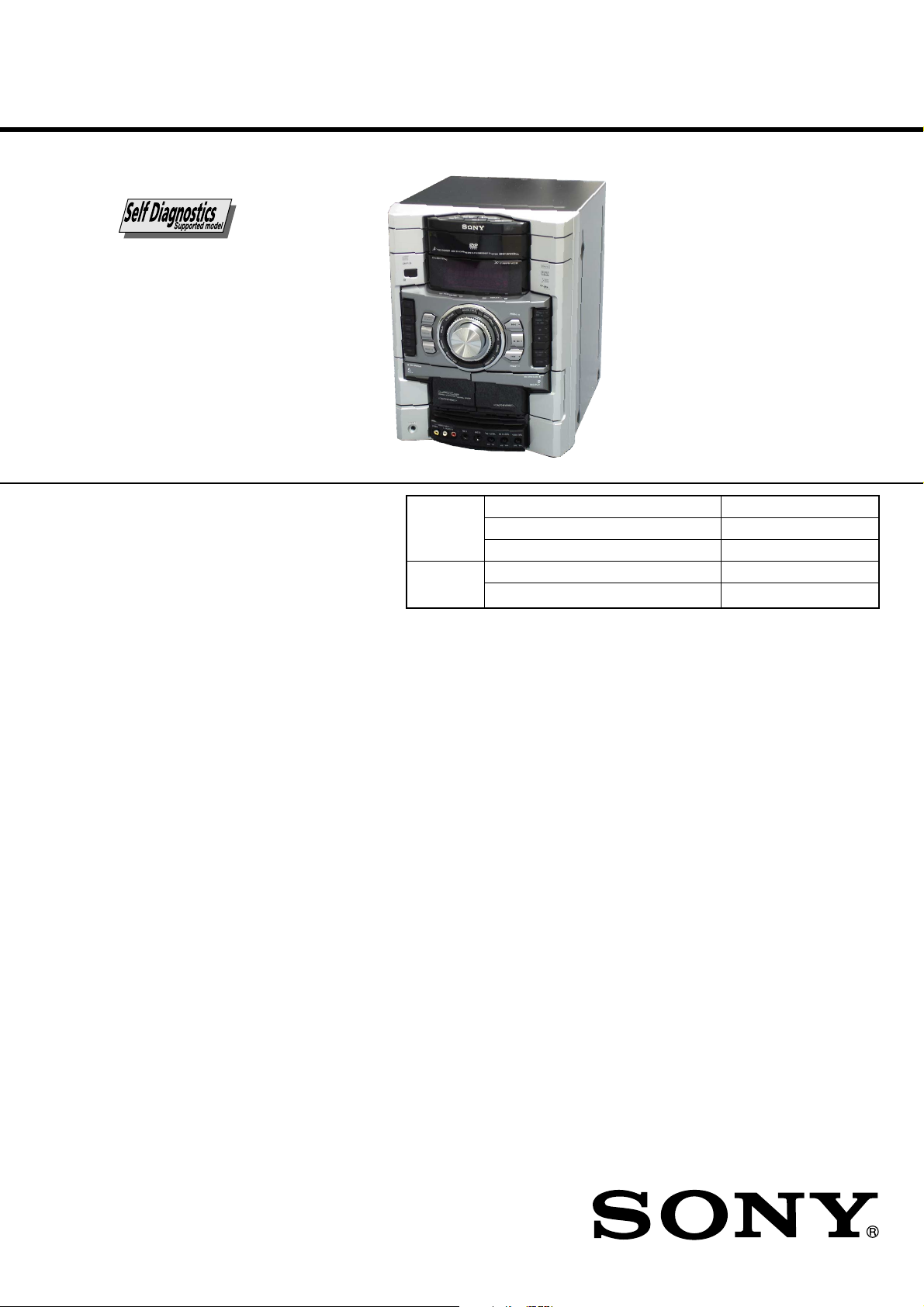
HCD-GN1100D
SERVICE MANUAL
Ver. 1.2 2007.10
• HCD-GN1100D is the Amplifier,
DVD player, tape deck and tuner
section in MHC-GN1100D.
DVD
Section
TAPE
Section
Model Name Using Similar Mechanism HCD-GN1000D
DVD Mechanism Type CDM74HF-DVBU101
Optical Pick-up Name KHM-313CAB/C2NP
Model Name Using Similar Mechanism HCD-GN1000D
Tape Transport Mechanism Type CWN42RR603
E Model
SPECIFICATIONS
Amplifier section
The following are measured at AC 120, 127, 220,
240V 50/60 Hz
Power output (rated): 130 W + 130 W
(6 Ω , 1 kHz, 1% THD)
RMS output power (reference)
Front speaker: 215 W + 215 W
(per channel at 6 Ω , 1 kHz, 10%
THD)
Center speaker: 85 W
(per channel at 6 Ω , 1 kHz, 10%
THD)
Surround speaker: 90 W + 90 W
(per channel at 6 Ω , 1 kHz, 10%
THD)
Subwoofer: 210 W (per channel at 8 Ω , at 100 Hz,
10% THD)
Inputs
VIDEO INPUT:
VIDEO: 1 Vp-p, 75 ohms
AUDIO L/R: Voltage 250 mV,
impedance 47 kilohms
TV/SAT AUDIO IN L/R:
Voltage 250 mV/450 mV, impedance
47 kilohms
MIC 1 or 2:
Sensitivity 1 mV, impedance
10 kilohms
Outputs
AUDIO OUT:
Voltage 250 mV, impedance 1 kilohm
VIDEO OUT:
Max. output level 1 Vp-p, unbalanced,
Sync. negative load impedance
75 ohms
COMPONENT VIDEO OUT:
Y: 1 Vp-p, 75 ohms
PB/CB: 0.7 Vp-p, 75 ohms
PR/CR: 0.7 Vp-p, 75 ohms
S VIDEO OUT:
Y: 1 Vp-p, unbalanced, Sync. negative
C: 0.286 Vp-p, load impedance
75 ohms
PHONES:
accepts headphones of 8 ohms or more
Disc player section
System
Compact disc and digital audio and
video system
Laser
Semiconductor laser (DVD: λ =650 nm,
CD: λ = 790 nm)
Emission duration: continuous
Frequency response
DVD (PCM 48 kHz): 2 Hz – 22 kHz
(±1 dB)
CD: 2 Hz – 20 kHz (±0.5 dB)
Video color system format
Latin American models: NTSC
Russian models: PAL
Other models: NTSC and PAL
– Continued on next page –
MINI HI-FI COMPONENT SYSTEM
9-887-683-03
2007J02-1
© 2007.10
Sony Corporation
Personal Audio Division
Published by Sony Techno Create Corporation
Page 2
HCD-GN1100D
Tape deck section
Recording system
4-track 2-channel stereo
Frequency response
50 – 13,000 Hz (±3 dB),
using Sony TYPE I tape
Tuner section
FM stereo, FM/AM superheterodyne tuner
FM tuner section
Tuning range
87.5 – 108.0 MHz (50 kHz step)
Antenna
FM lead antenna
Antenna terminals
75 ohms unbalanced
Intermediate frequency
10.7 MHz
AM tuner section
Tuning range
Saudi Arabian:
531 – 1,602 kHz (with the interval set
at 9 kHz)
Other models:
531 – 1,602 kHz (with the interval set
at 9 kHz)
530 – 1,710 kHz (with the interval set
at 10 kHz)
Antenna
AM loop antenna
Antenna terminals
External antenna terminal
Intermediate frequency
450 kHz
General
Power requirements
Saudi Arabian model: 120 – 127 V,
220 V or 230 – 240 V AC, 50/60 Hz,
adjustable with voltage selector
Thai model: 220 V AC, 50/60 Hz
Other models: 120 V, 220 V or
230 – 240 V AC, 50/60 Hz, adjustable
with voltage selector
Power consumption
350 W
Dimensions (w/h/d) (Approx.)
281 × 361 × 417 mm
Mass (Approx.)
16.0 kg
Self-diagnosis Function
(When letters/numbers appear in the
display)
When the self-diagnosis function is activated to
prevent the system from malfunctioning, a
5-character service number (e.g. C 13 50) with a
combination of a letter and 4 digits appears on
the TV screen and the front panel display. In this
case, check the following table.
First 3
characters of
the service
number
C 13 This disc is dirty.
C 31 The disc is not inserted correctly.
E XX
(XX is a
number)
When displaying the version number on the
TV screen
When you turn on the system, the version
number [VER.X.XX] (X is a number) may
appear on the TV screen. Although this is not a
malfunction and for Sony service use only,
normal system operation will not be possible.
Turn off the system, and then turn on the system
again to operate.
Cause and corrective action
Clean the disc with a soft cloth
Restart the system, then re-insert
the disc correctly.
To prevent a malfunction, the system
has performed the self-diagnosis
function.
Contact your nearest Sony dealer or
local authorized Sony service
facility and give the 5-character
service number.
Example: E 61 10
VER.X.XX
Design and specifications are subject to change without notice.
2
Page 3

TABLE OF CONTENTS
HCD-GN1100D
1. SERVICING NOTES ................................................ 4
2. GENERAL ................................................................... 5
3. DISASSEMBLY
3-1. Disassembly Flow ........................................................... 7
3-2. Case ................................................................................. 8
3-3. Loading Panel.................................................................. 8
3-4. Tuner Pack....................................................................... 9
3-5. DVD Mechanism Deck ................................................... 9
3-6. Front Panel Assy.............................................................. 10
3-7. Tape Mechanism Deck, MIC Board ................................ 10
3-8. CD-SW Board ................................................................. 11
3-9. PANEL Board, FUNCTION Board, JOG Board............. 11
3-10. KARAOKE Board, VIDEO Board, DMB16 Board ........ 12
3-11. Back Panel ....................................................................... 12
3-12. PRIMARY Board, EFFECTOR Board............................ 13
3-13. Power AMP PC Board Assy, MAIN Board ..................... 13
3-14. SURROUND Board, PA Board ....................................... 14
3-15. Power Transformer (T1200) ........................................... 14
3-16. DRIVER Board, SW Board ............................................. 15
3-17. DVD Assy ........................................................................ 15
3-18. Optical Pick-up ................................................................ 16
3-19. SENSOR Board ............................................................... 16
3-20. MOTOR (TB) Board ....................................................... 17
3-21. MOTOR (LD) Board ....................................................... 17
4. TEST MODE ............................................................... 18
5. MECHANICAL ADJUSTMENTS......................... 23
6. ELECTRICAL ADJUSTMENTS .......................... 23
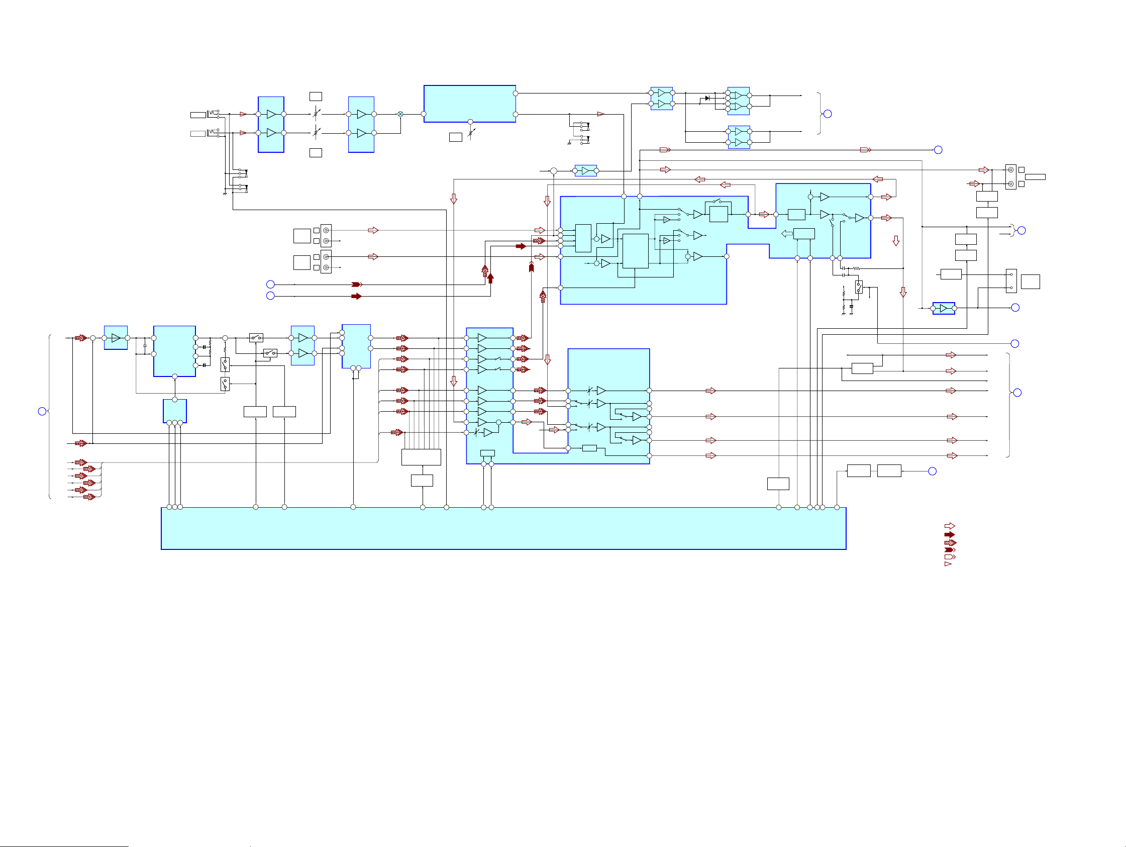
7. DIAGRAMS .......................................................... 25
7-1. Block Diagram – RF Section –....................................... 27
7-2. Block Diagram – Video Section – ................................... 28
7-3. Block Diagram – Tape/Tuner Section – .......................... 29
7-4. Block Diagram – Main Section – .................................... 30
7-5. Block Diagram – AMP Section – .................................... 31
7-6. Block Diagram – Display/Power Section –..................... 32
7-7. Printed Wiring Board – DMB16 Board (Side A) – ......... 33
7-8. Printed Wiring Board – DMB16 Board (Side B) – ........ 34
7-9. Schematic Diagram – DMB16 Board (1/4) –................ 35
7-10. Schematic Diagram – DMB16 Board (2/4) – ................ 36
7-11. Schematic Diagram – DMB16 Board (3/4) – ................ 37
7-12. Schematic Diagram – DMB16 Board (4/4) – ................ 38
7-13. Printed Wiring Boards – CD Mechanism Boards – ....... 39
7-14. Schematic Diagram – CD Mechanism Boards – ........... 40
7-15. Printed Wiring Board – MAIN Board – .......................... 41
7-16. Schematic Diagram – MAIN Board (1/5) – ................... 42
7-17. Schematic Diagram – MAIN Board (2/5) – ................... 43
7-18. Schematic Diagram – MAIN Board (3/5) – ................... 44
7-19. Schematic Diagram – MAIN Board (4/5) – ................... 45
7-20. Schematic Diagram – MAIN Board (5/5) – ................... 46
7-21. Printed Wiring Board – PANEL Board – ........................ 47
7-22. Schematic Diagram – PANEL Board – .......................... 48
7-23. Printed Wiring Boards – CD-SW, JOG, FUNCTION
And MIC Boards – .......................................................... 49
7-24. Schematic Diagram – CD-SW, JOG, FUNCTION
And MIC Boards – .......................................................... 50
7-25. Printed Wiring Board – PA Board – ................................ 51
7-26. Schematic Diagram – PA Board – .................................. 52
7-27. Printed Wiring Board – SURROUND Board – ............... 53
7-28. Schematic Diagram – SURROUND Board (1/2) – ........ 54
7-29. Schematic Diagram – SURROUND Board (2/2) – ....... 55
7-30. Printed Wiring Board – EFFECTOR Board – ................. 56
7-31. Schematic Diagram – EFFECTOR Board – ................... 57
7-32. Printed Wiring Board – VIDEO Board – ........................ 58
7-33. Schematic Diagram – VIDEO Board – .......................... 59
7-34. Printed Wiring Boards – Power Section – ....................... 60
7-35. Schematic Diagram – Power Section – .......................... 61
7-36. Printed Wiring Board – KARAOKE Board – ................. 62
7-37. Schematic Diagram – KARAOKE Board – ................... 62
7-38. IC Pin Function Description ............................................ 65
8. EXPLODED VIEWS
8-1. Case, Back Panel Section ................................................ 75
8-2. Front Panel Section-1 ...................................................... 76
8-3. Front Panel Section-2 ...................................................... 77
8-4. Chassis Section................................................................ 78
8-5. DVD Mechanism Section-1 (CDM74HF-DVBU101).... 79
8-6. DVD Mechanism Section-2 (CDM74HF-DVBU101).... 80
9. ELECTRICAL PARTS LIST .................................. 81
3
Page 4

HCD-GN1100D
Ver. 1.2
SECTION 1
SERVICING NOTES
NOTES ON HANDLING THE OPTICAL PICK-UP BLOCK
OR BASE UNIT
The laser diode in the optical pick-up block may suffer electrostatic
break-down because of the potential difference generated by the
charged electrostatic load, etc. on clothing and the human body.
During repair, pay attention to electrostatic break-down and also
use the procedure in the printed matter which is included in the
repair parts.
The flexible board is easily damaged and should be handled with
care.
NOTES ON LASER DIODE EMISSION CHECK
The laser beam on this model is concentrated so as to be focused on
the disc reflective surface by the objective lens in the optical pickup block. Therefore, when checking the laser diode emission,
observe from more than 30 cm away from the objective lens.
LASER DIODE AND FOCUS SEARCH OPERATION
CHECK
Carry out the “S curve check” in “CD section adjustment” and check
that the S curve waveform is output several times.
CAUTION
Use of controls or adjustments or performance of procedures
other than those specified herein may result in hazardous
radiation exposure.
UNLEADED SOLDER
Boards requiring use of unleaded solder are printed with the leadfree mark (LF) indicating the solder contains no lead.
(Caution: Some printed circuit boards may not come printed with
the lead free mark due to their particular size)
: LEAD FREE MARK
Unleaded solder has the following characteristics.
• Unleaded solder melts at a temperature about 40 °C higher
than ordinary solder.
Ordinary soldering irons can be used but the iron tip has to be
applied to the solder joint for a slightly longer time.
Soldering irons using a temperature regulator should be set to
about 350 °C.
Caution: The printed pattern (copper foil) may peel away if
the heated tip is applied for too long, so be careful!
• Strong viscosity
Unleaded solder is more viscou-s (sticky, less prone to flow)
than ordinary solder so use caution not to let solder bridges
occur such as on IC pins, etc.
• Usable with ordinary solder
It is best to use only unleaded solder but unleaded solder may
also be added to ordinary solder.
• MODEL IDENTIFICATION
– Back Panel –
PART No.
This appliance is classified as
a CLASS 1 LASER product.
This label is located on the rear
exterior.
Notes on chip component replacement
• Never reuse a disconnected chip component.
• Notice that the minus side of a tantalum capacitor may be
damaged by heat.
Flexible Circuit Board Repairing
• Keep the temperature of soldering iron around 270˚C
during repairing.
• Do not touch the soldering iron on the same conductor of the
circuit board (within 3 times).
• Be careful not to apply force on the conductor when soldering
or unsoldering.
SAFETY-RELATED COMPONENT WARNING!!
COMPONENTS IDENTIFIED BY MARK 0 OR DOTTED LINE WITH
MARK 0 ON THE SCHEMATIC DIAGRAMS AND IN THE PARTS
LIST ARE CRITICAL TO SAFE OPERATION. REPLACE THESE
COMPONENTS WITH SONY PARTS WHOSE PART NUMBERS
APPEAR AS SHOWN IN THIS MANUAL OR IN SUPPLEMENTS
PUBLISHED BY SONY .
MODEL PART No.
E3, E15 models 3-197-993-0[]
EA model 3-197-994-0[]
E12 model 3-197-995-0[]
MY, SP models 3-197-996-0[]
TH model 3-197-998-0[]
PH model 3-197-999-0[]
• Abbreviation
E3 : 240V AC Area in E model
E12 : 220V-240V AC Area in E model
E15 : Iran model
EA : Saudi Arabia model
MY : Malaysia model
PH : Philippines model
SP : Singapore model
TH : Thai model
4
Page 5
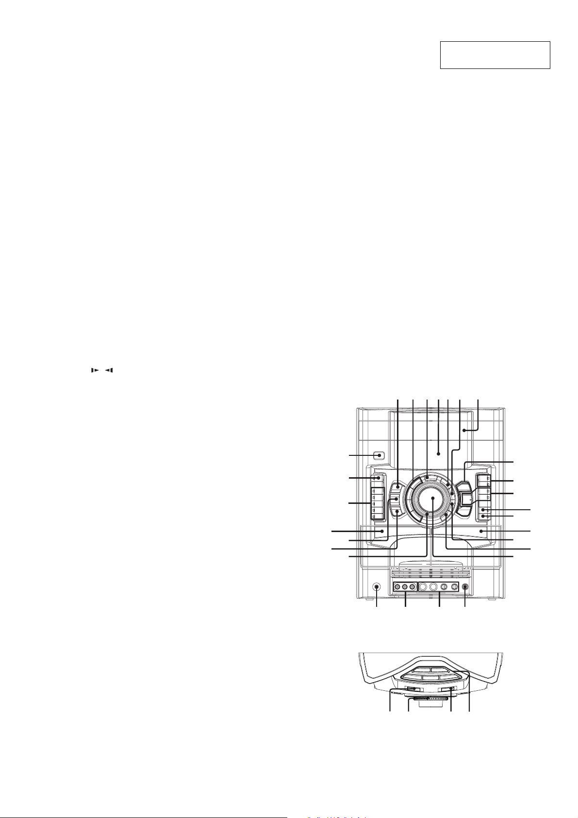
LOCA TING THE CONTROLS
q
q
q
w
SECTION 2
GENERAL
HCD-GN1100D
This section is extracted
from instruction manual.
1 EQ BAND/MEMORY
Press to select a frequency band
when adjusting the graphic
equalizer.
B FLANGER
DELAY
CHORUS
SOUND FLASH
Press to create a party atmosphere.
C SOUND FIELD
Press to select a sound field.
D Display
E AMP MENU
Press to change the spectrum
analyser display or to adjust the
brightness of the display.
F PROGRESSIVE
Press to select the format of the video
signals output from the
COMPONENT VIDEO OUT jacks.
G Disc tray
H PRESET +/–
Press to select a preset station.
>/. (go forward/go
backward)
Press to go forward or go backward.
I TUNING +/–
Press to tune in a radio station.
M/m (fast forward/
rewind)
Press to fast forward or rewind.
J nN (play)
x (stop)
X (pause)
Press to start, stop or pause playback.
K REC PAUSE/START
Press to start recording.
L CD SYNC
Press to select CD Synchro
Recording.
M B PUSH OPEN/CLOSE Z
(Eject B)
Press to insert or eject tape B.
Deck B
N ENTER
Press to select or enter the selection.
O DIRECTION
Press to select the tape playback
option.
P MASTER VOLUME
Turn to adjust the volume.
Q ECHO LEVEL
Turn to adjust the microphone echo
effect.
R MIC 1/2 (jack)
Connect the microphones.
MIC 1/2 LEVEL
Turn to adjust the microphone
volume.
S VIDEO INPUT (jacks)
Connect an audio or video
component.
T PHONES (jack)
Connect the headphones.
U Power illuminator
V PRESET EQ
Press to select a preset effect.
W GROOVE
Press to reinforce the bass.
X A Z PUSH OPEN/CLOSE
(Eject A)
Press to insert or eject tape A.
Deck A
Y DVD
TUNER/BAND
TAPE A/B
TV/SAT
VIDEO
Press to select a function.
Z "/1 (on/standby)
Press to turn the unit on or off.
wj IR Receptor
wk ILLUMINATION
Press to change the power
illuminator.
wl OPERATION DIAL
Turn to select a setting.
e; DISPLAY
Press to display disc information in
the front panel display or to change
the front panel display during Power
Saving Mode.
ea DISC SKIP/EX-CHANGE
Press to exchange other discs during
playback.
Z OPEN/CLOSE
Press to load or eject a disc.
DISC 1 ~ 3
Press to select a disc.
Front panel
wj
wh
wg
wf
wd
ws
2
413
5
6
7
8
9
q;
qs
qf
qhwa
qa
qd
qg
j
l
;
k
Top panel
wk wl e; ea
5
Page 6
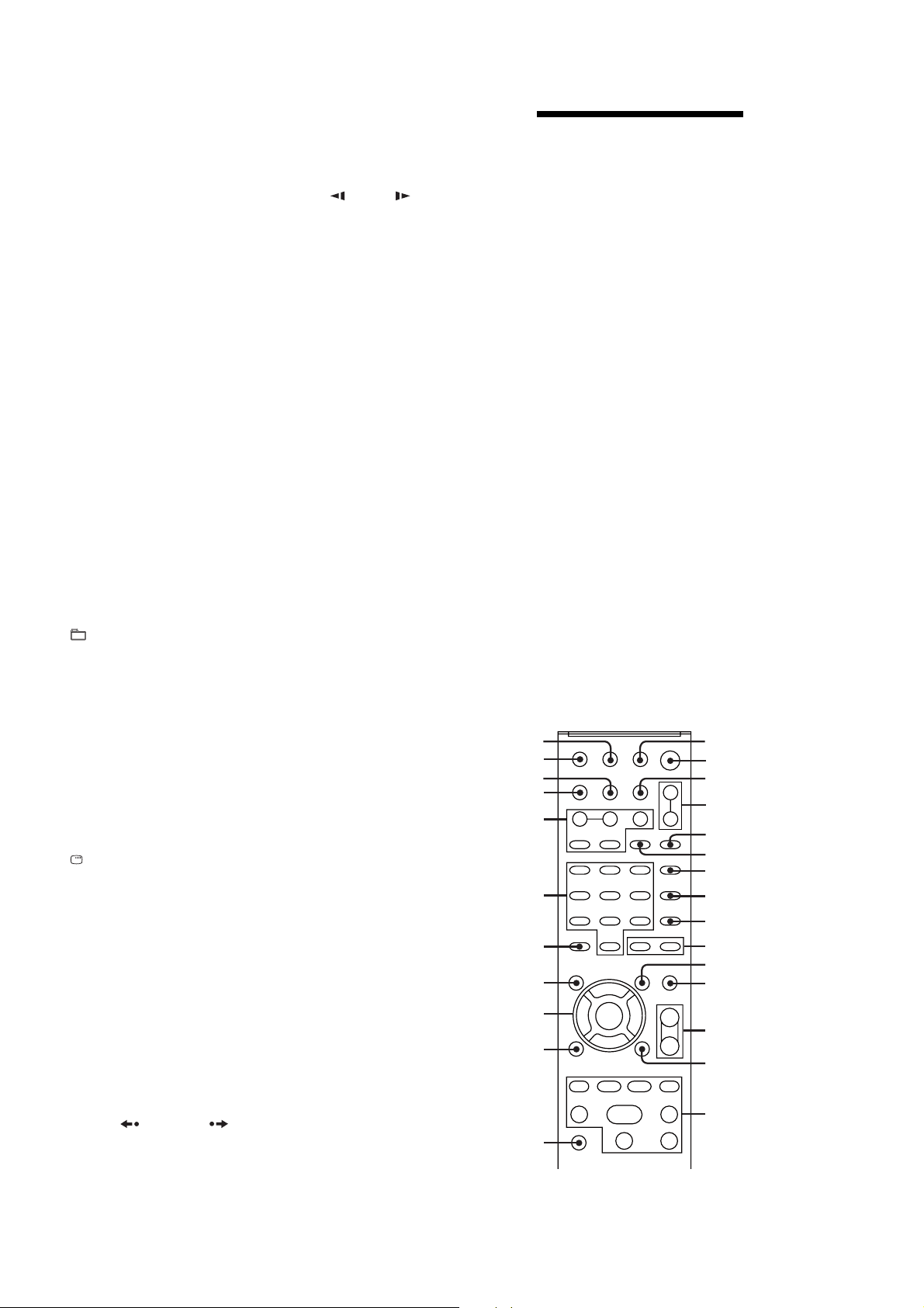
HCD-GN1100D
REMOTE CONTROL
1 THEATRE SYNC
Press to operate the THEATRE
SYNC function.
B TV "/1 (on/standby)
Press to turn the TV on or off.
"/1 (on/standby)
Press to turn the unit on or off.
C DISC SKIP
Press to skip a disc.
D FUNCTION +/–
Press to select a function.
E PICTURE NAVI
Press to search for a scene or a file.
F REPEAT/FM MODE
Press to change the Repeat Play
setting.
Press to select the FM monaural or
stereo reception.
G AUDIO
Press to select the audio format.
H SUBTITLE/D.TUNING
Press to turn off or change the
language of the subtitle.
Press to enter direct tuning mode.
I ANGLE
Press to change the angle.
J
Press to select an album.
K DVD/TUNER MENU
Press to display the menu of the
DVD player.
Press to preset a radio station.
L SOUND FIELD
Press to select a sound field.
M TV VOL +/–*
Press to adjust the TV volume.
VOLUME +/–*
Press to adjust the volume.
N DISPLAY
Press to turn on or off or change the
Control Menu display on the TV
screen.
O TV CH +/–
Press to select a TV channel.
PRESET +/–
Press to select a preset station.
./> (go backward/go
forward)
Press to go backward or go forward.
c STEP C
Press to watch one frame at a time.
REPLAY /ADVANCE
Press to replay the previous scene or
fast forward the current scene.
TUNING +/–
Press to tune in a radio station.
SLOW /SLOW
Press to watch frame by frame.
m/M (rewind/fast forward
Press to rewind or fast forward.
H* (play)
X (pause)
x (stop)
Press to start, pause or stop playback.
P TV
Hold down TV and press the button
you want to operate the TV.
Q O RETURN
Press to return to the previous
display.
R V/v/B/b
Press to select the settings.
ENTER
Press to enter the selection.
S DVD TOP MENU
Press to display the DVD title.
T -/--
Press to enter a double digit channel
number for TV.
CLEAR
Press to cancel the play mode or clear
a mistake when you press the
incorrect numeric button.
U Numeric buttons*
Press to tune or preset a radio station,
enter a track or file number, etc.
V KEY CONTROL 2/#
SCORE
KARAOKE MODE
KARAOKE PON
Press to enjoy the karaoke function.
W DISPLAY
Press to display disc information in
the front panel display or to change
the front panel display during Power
Saving Mode.
wf TIME/TEXT
Press to check the elapsed playing
time, remaining time, etc.
wg TV INPUT
Press to switch the TV’s input
source.
SLEEP
Press to activate the sleep timer.
wh TIMER MENU
Press to set the time and timer.
*The numeric button 5, TV VOL +, VOLUME
+ and H buttons have a tactile dot. Use the
tactile dot as a reference when operating the
system.
Setting the clock
Press "/1 to turn on the system.
1
2
Press TIMER MENU.
The hour indication flashes in the
display.
If “PLAY SET?” flashes in the
display, press
select “CLOCK SET?”, then press
ENTER.
3
Press V or v repeatedly to set
the hour.
4
Press ENTER.
The minute indication flashes in the
display.
5
Press V or v repeatedly to set
the minute.
6
Press ENTER.
The clock starts functioning.
Note
The clock settings are canceled when you
disconnect the power cord or if a power failure
occurs.
wh
wg
wf
wd
ws
wa
w;
ql
qk
qj
qh
V
or v repeatedly to
1
2
3
4
5
6
7
8
9
q;
qa
qs
qd
qf
qg
6
Page 7
Note:
• This set can be disassembled in the order shown below.
3-1. DISASSEMBLY FLOW
SET
3-2. CASE
(Page 8)
3-3. LOADING PANEL
(Page 8)
3-4. TUNER P A CK
(Page 9)
HCD-GN1100D
SECTION 3
DISASSEMBLY
3-5. DVD MECHANISM DECK
(Page 9)
3-6. FRONT PANEL ASSY
(Page 10)
3-11. BACK PANEL
(Page 12)
3-10. KARAOKE BOARD,
VIDEO BOARD,
DMB16 BOARD,
(Page 12)
3-16. DRIVER BOARD,
SW BOARD
(Page 15)
3-7. TAPE MECHANISM DECK,
MIC BOARD
(Page 10)
3-17. DVD ASSY
(Page 15)
3-18. OPTICAL PICK-UP
(Page 16)
3-8. CD-SW BOARD
(Page 11)
3-19. SENSOR BOARD
(Page 16)
3-20. MOTOR (TB) BOARD
(Page 17)
3-21. MOTOR (LD) BOARD
(Page 17)
3-13. POWER AMP PC BOARD ASSY,
MAIN BOARD
(Page 13)
3-14. SURROUND BOARD,
PA BOARD
(Page 14)
3-12. PRIMARY BOARD
EFFECTOR BOARD
(Page 13)
3-9. PANEL BOARD,
FUNCTION BOARD,
JOG BOARD
(Page 11)
3-15. POWER TRANSFORMER
(T1200)
(Page 14)
7
Page 8
HCD-GN1100D
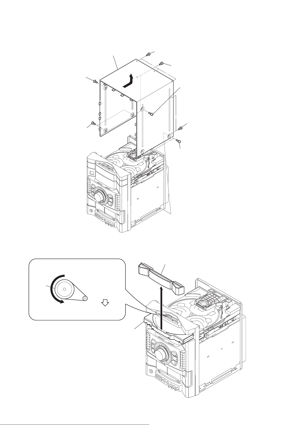
3-2. CASE
4
screw
(case 3 TP2)
(3
×
12)
two screws
3
(case 3 TP2)
(3
×
8)
9
case
8
7
three screws
(+BVTP 3
6
(+BVTP 3
×
10)
two screws
1
(case 3 TP2)
(3
×
10)
2
screw (case 3 TP2)
×
12)
(3
5
two screws
(+BVTP 3
two screws
×
8)
×
10)
3-3. LOADING PANEL
DVD mechanism deck (CDM74HF-DVBU101)
1
Turn the pulley to the arrow direction.
Pulley
Front side
2
Pull out disc tray.
3
4
loading panel
8
Page 9
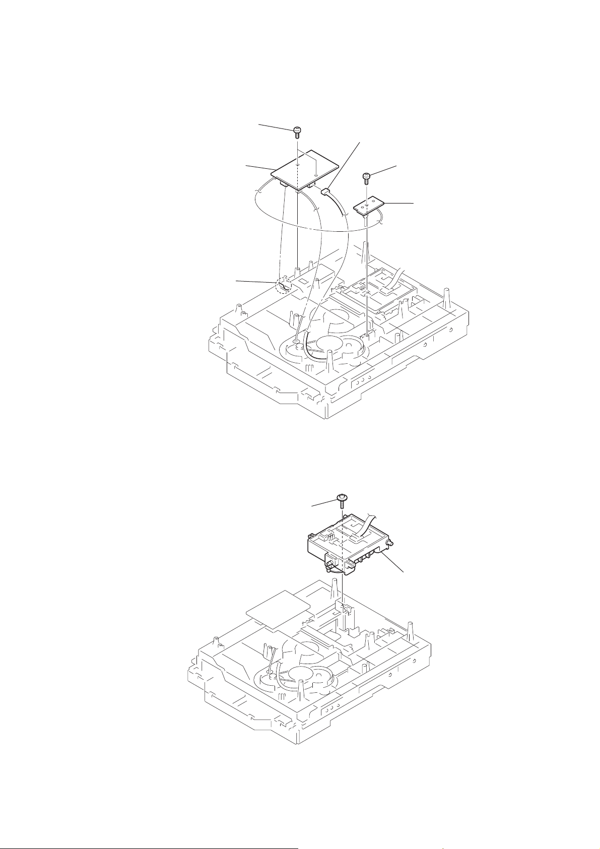
3-4. TUNER PACK
)
2
wire (flat type)
(CN1)
3
tuner pack
1
two screws
(+BVTP 3×8
HCD-GN1100D
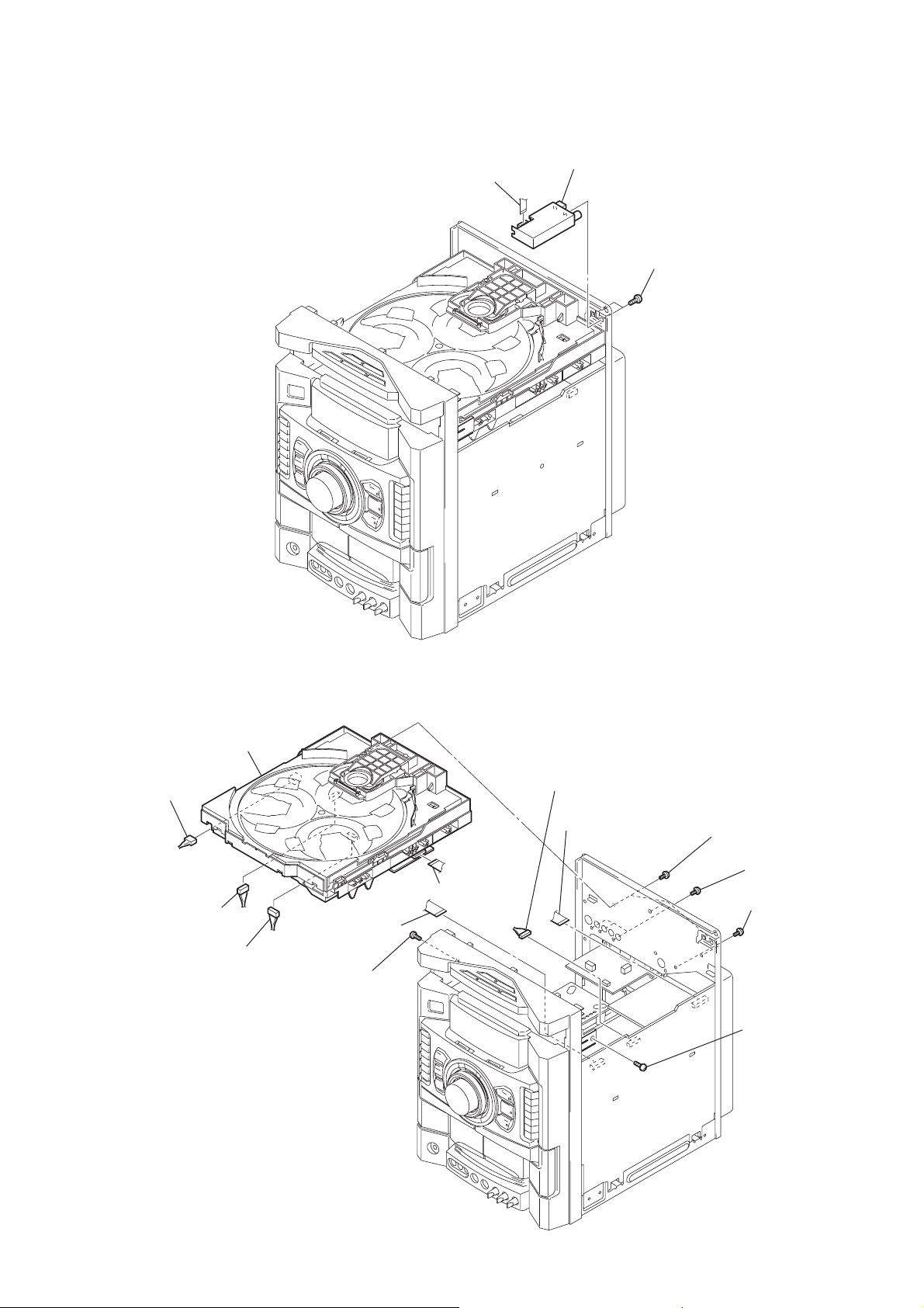
3-5. DVD MECHANISM DECK
6
DVD mechanism deck
qd
connector
(CN802)
qs
connector
(CN800)
qa
connector
(CN401)
0
(CN520)
wire (flat type)
5
screw
×
(+P 3
12)
7
wire (flat type)
(CN701)
9
connector
(CN505)
8
wire (flat type)
(CN521)
3
three screws
(+BVTP 3
1
three screws
(+BVTP 3
2
screw
(+BVTP 3
4
screw
(+P 3
×
10)
×
10)
×
10)
×
12)
9
Page 10
HCD-GN1100D
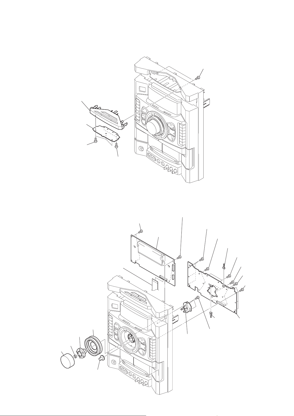
3-6. FRONT PANEL ASSY
3
front panel assy
6
wire (flat type)
(CN509)
5
wire (flat type)
(CN508)
8
(CN907)
connector
4
connector
(CN100)
1
three screws
(+BVTP 3×8)
3-7. TAPE MECHANISM DECK, MIC BOARD
2
three screws
(+BVTP 3×8)
7
connector
(CN504)
9
connector
(CN503)
1
three screws
(+BVTP2.6 (3CR))
4
2
screw
(+BVTP2.6 (3CR))
3
two screws
(+BVTP2.6 (3CR))
tape mechanism deck
10
5
knob (MIC)
6
two screws
(+BVTP2.6 (3CR))
7
bracket (MIC SHIELD)
9
MIC board
8
two screws
(+BVTP2.6 (3CR))
Page 11
3-8. CD-SW BOARD
)
)
5
CD-SW board
3
three screws
(+BTTP (M2.6))
2
escutcheon (CD)
HCD-GN1100D
1
two screws
(+BVTP2.6 (3CR)
4
two screws
(+BTTP (M2.6))
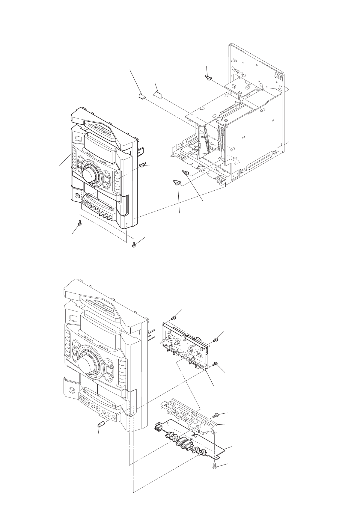
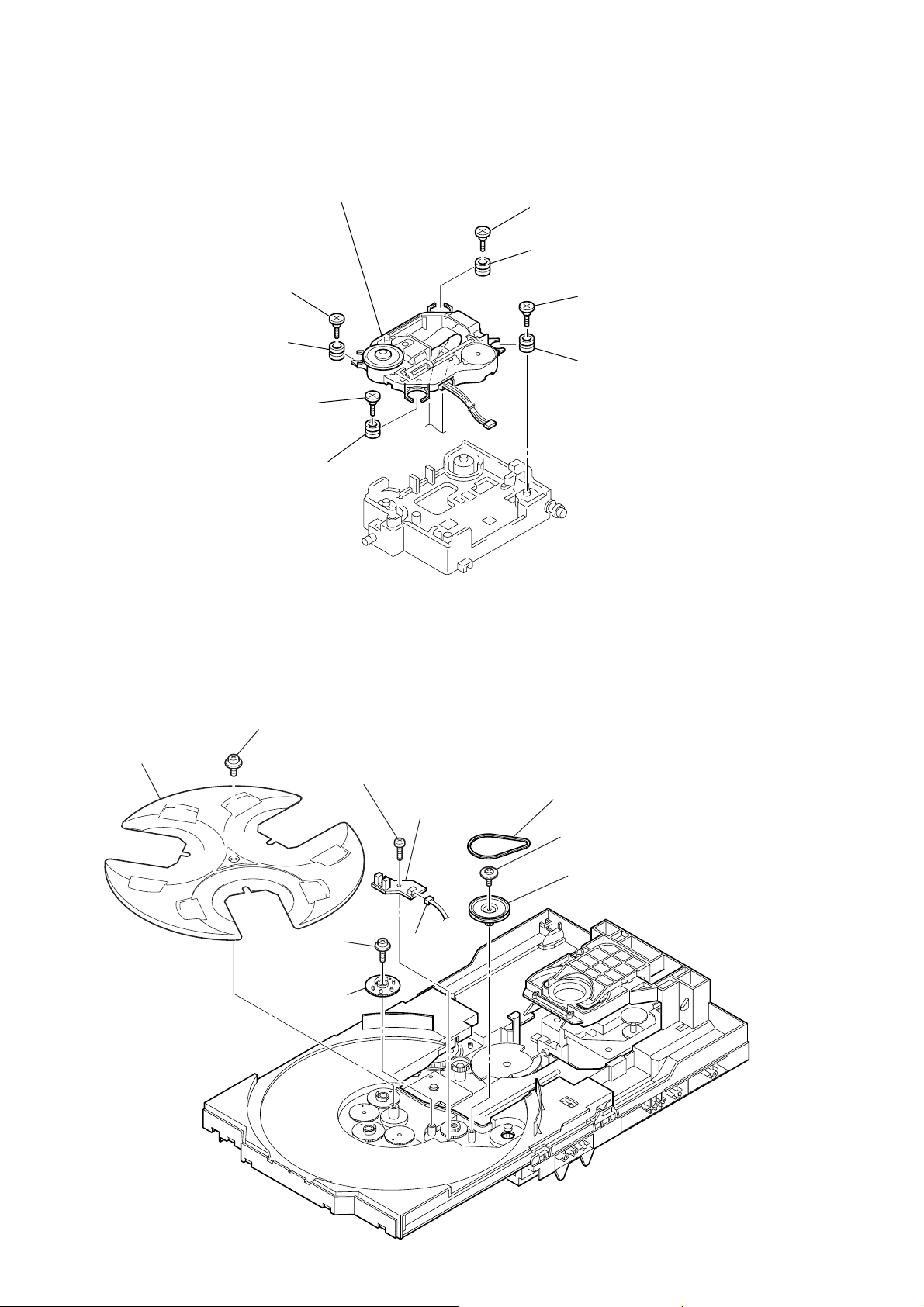
3-9. PANEL BOARD, FUNCTION BOARD, JOG BOARD
6
two screws
(+BVTP2.6 (3CR))
9
PANEL board
8
wire (flat type)
(CN900)
7
two screws
(+BVTP2.6 (3CR))
qg
four screws
(+BVTP2.6 (3CR))
qf
three screws
(+BVTP2.6 (3CR))
qk
connector
(CN905)
qd
two screws
(+BVTP2.6 (3CR))
qs
two screws
(+BVTP2.6 (3CR))
qa
four screws
(+BVTP2.6 (3CR))
0
(+BVTP2.6 (3CR)
four screws
1
Knob (VOLUME)
3
holder (JOG)
2
nut
4
knob jog assy
5
gear (ENCODER)
w;
JOG board
qj
connector
(CN904)
ql
three screws
(+BVTP2.6 (3CR))
qh
FUNCTION board
11
Page 12
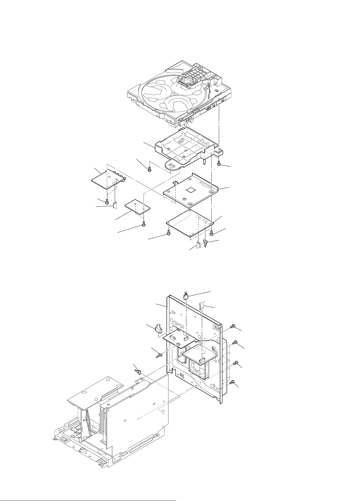
HCD-GN1100D
)
3-10. KARAOKE BOARD, VIDEO BOARD,
DMB16 BOARD
8
CDM cover
6
5
VIDEO board
screw
(+BVTP 3
×
10)
7
two screws
(+BVTP 3
×
10)
4
(+BVTP 3
3
wire (flat type)
(CN801)
3-11. BACK PANEL
two screws
×
2
KARAOKE board
1
two screws
(+BVTP 3
10)
×
10)
qs
two screws
(+BVTP 3
9
back panel
2
connector
(CN1204) : except TH
(CN1205) : TH
1
connector
(CN1200)
0
connector
(CN580)
×
10)
0
(CN101)
wire (flat type)
qf
qd
DMB16 board
qa
two screws
(+BVTP 3
9
connector
(CN201)
3
connector
(CN1202)
4
wire (flat type)
(CN1502)
bracket (mediatec)
×
10)
6
two screws
(+BVTP 3
5
seven screws
(+BVTP 3×10)
8
two screws
(+BVTP 3×10)
×
10)
12
7
screw (+BVTP 3×10
Page 13
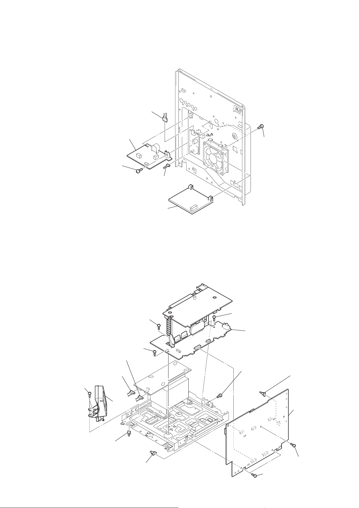
3-12. PRIMARY BOARD, EFFECTOR BOARD
)
1
connector
(CN101)
4
PRIMARY board
3
screw
(+BVTP 3
×
8)
2
(CN201)
connector
5
two screws
(+BVTP 3
HCD-GN1100D
×
10)
6
EFFECTOR board
3-13. POWER AMP PC BOARD ASSY, MAIN BOARD
8
two screws
(+BV3 (3-CR))
7
screw
(+BV3 (3-CR))
5
connector
(CN1216)
2
two screws
(+BV3 (3-CR))
4
connector
(CN1213)
9
screw
(+BV3 (3-CR))
qa
power AMP PC board assy
0
screw
(+BVTP 3×10)
qs
connector
(CN105)
3
DC fan
6
connector
(CN1215)
1
connector
(CN582)
qd
two screws
(+BVTP 3×8)
qg
MAIN board
qf
screw
(+BVTP 3×8
13
Page 14
HCD-GN1100D
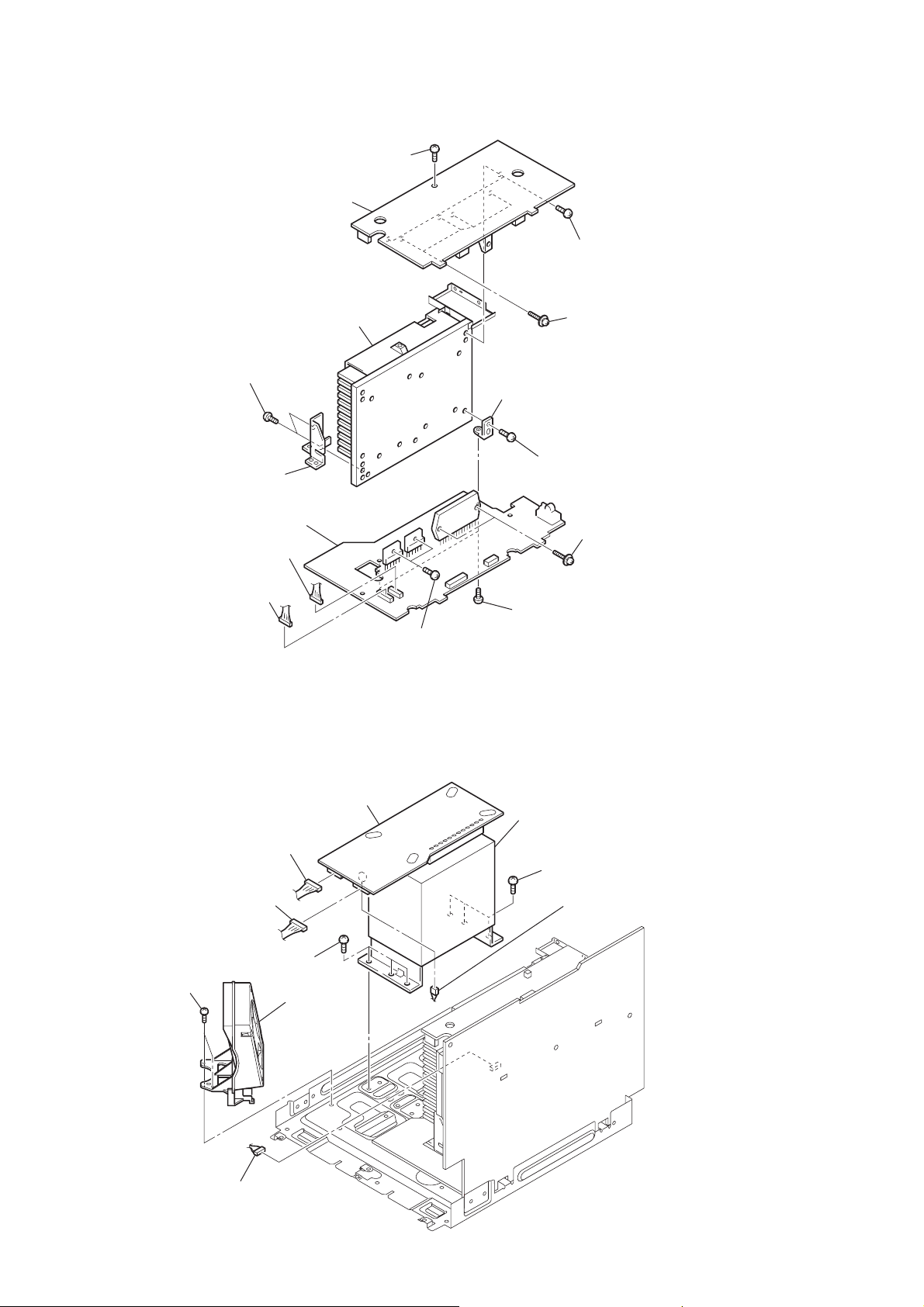
3-14. SURROUND BOARD, PA BOARD
3
screw (+BV3 (3-CR))
4
SURROUND board
qs
7
two screws
(+BVTP 3
8
holder
×
10)
heat sink
qf
bracket
2
two screws
(+BVTP 3
1
four screws
(transistor)
qd
screw
(+BVTP 3
×
10)
×
10)
qg
PA board
6
connector
(CN607)
5
connector
(CN602)
3-15. POWER TRANSFORMER (T1200)
4
connector
(CN1213)
5
connector
(CN1216)
7
2
two screws
(+BV3 (3-CR))
three screws
3
DC fan
(M892)
TRANS board
qa
two screws
(+BVTP 3
9
(+BVTP 3
×
10)
9
0
two screws
(transistor)
two screws
power transfomer (T1200)
×
8
three screws
6
connector
(CN1215)
10)
14
1
connector
(CN582)
Page 15
3-16. DRIVER BOARD, SW BOARD
1
two
screws
(+BTTP (M2.6))
4
DRIVER
2
(CN702)
board
wire (flat type)
3
connector (CN703)
5
screw
(+BTTP (M2.6))
6
SW board
HCD-GN1100D
3-17. DVD ASSY
1
floating
(+PTPWH M2.6)
screw
2
DVD
assy
15
Page 16
HCD-GN1100D
w
3-18. OPTICAL PICK-UP
3
insulator screw
8
insulator
4
insulator screw
9
insulator
5
optical pick-up
(KHM-313CAB/C2NP)
2
insulator screw
7
insulator
1
6
insulator scre
insulator
3-19. SENSOR BOARD
2
t
ray
1
floating
(+PTPWH M2.6)
6
floating
(+PTPWH M2.6)
7
g
screw
8
(+BTTP (M2.6))
screw
ear (geneva)
s
crew
0
SENSOR board
9
connector
(
CN731)
3
b
elt (table)
4
floating
(+PTPWH M2.6)
5
screw
p
ulley (table)
16
Page 17
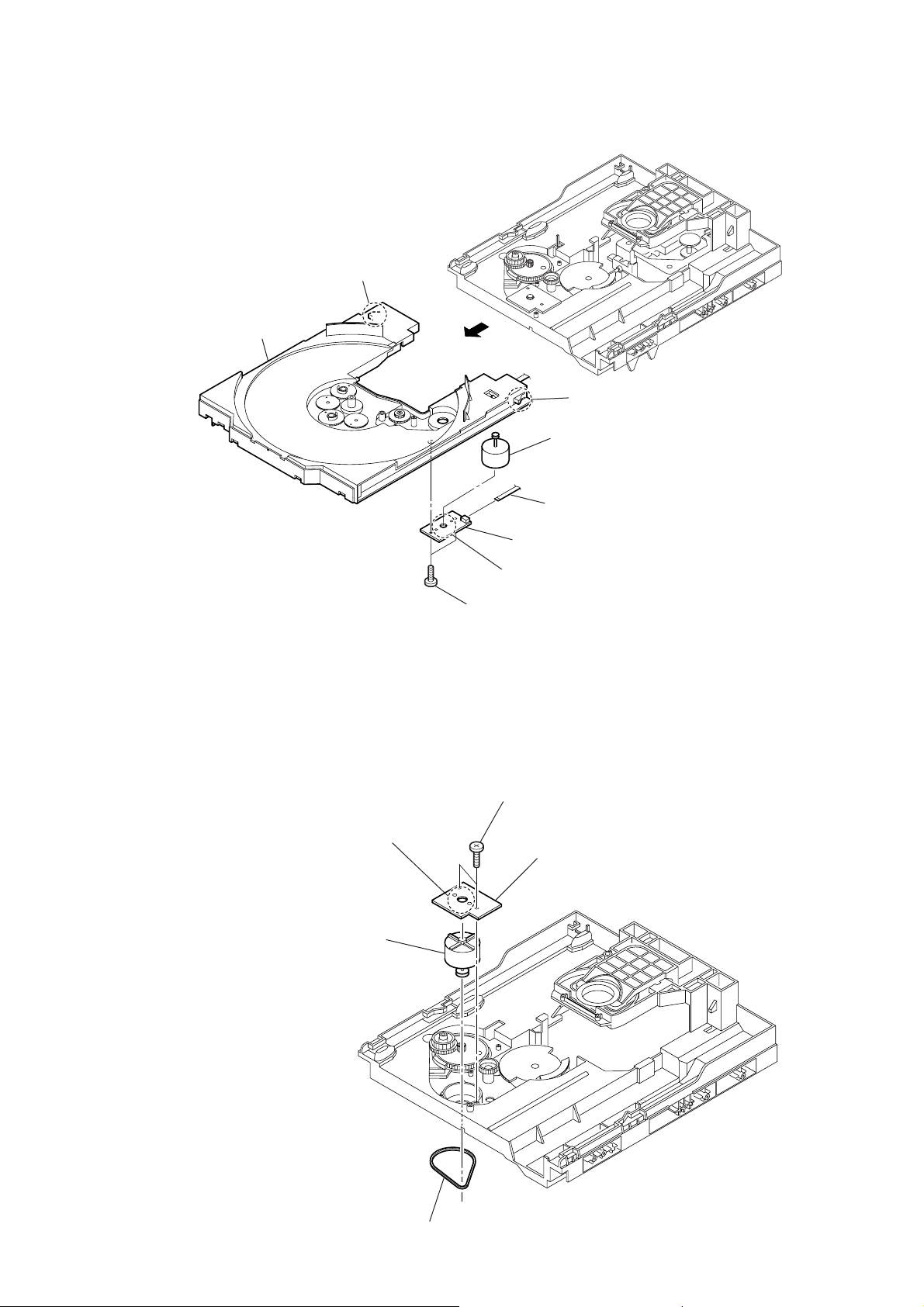
3-20. MOTOR (TB) BOARD
2
HCD-GN1100D
stopper
table
3-21. MOTOR (LD) BOARD
4
8
6
Remove the two solderings of motor.
5
two
screws
(+BTTP (M2.6))
1
stopper
7
t
able motor assy (M741)
wire (flat type) (CN742)
3
MOTOR (TB) board
2
Remove the two solderings of motor.
5
l
oading motor assy (M751)
1
b
elt (loading)
3
two
screws
(+BTTP (M2.6))
4
MOTOR (LD) board
17
Page 18

HCD-GN1100D
SECTION 4
TEST MODE
[P ANEL TEST MODE]
• This mode is used to check the fluorescent indicator tube, LEDs,
buttons, MASTER VOLUME knob, OPERATION DIAL knob,
model, destination, software version.
Procedure:
1. Press
2. All LEDs and segments in fluorescent indicator tube are lighted up.
3. When you want to enter to the software version display mode,
4. Each time
5. Press
6. In the key check mode, the fluorescent indicator tube displays
7. When
8. To release from this mode, press three buttons in the same
x
button, [ENTER] button and [DISC 2] button
simultaneously.
All LEDs are lighted up in red color except for
the LED is lighted up in green color.
press [DISC 1] button. The model information appears on the
fluorescent indicator tube.
b B
LED where
[DISC 1] button is pressed, the display changes from
MC version, GC version, SYS version, DVD version, ST
version, TC version, TA version, TM version in this order, and
returns to the model information display.
[DISC 2] button, the key check mode is activated.
“K 0 J0 V0”.
Turn the [OPERATIONAL DIAL] clockwise; “J” value increases
by one. Turn the [OPERATIONAL DIAL] counterclockwise; “J”
value decreases by one. Each time a button is pressed, “K” value
increases. Press other keys on main unit to check whether the
key is detected. However, once a button has been pressed, it is
no longer taken into account.
“V” value increases in the manner of 0,1, 2, 3 ... if [MASTER
VOLUME] knob is turned clockwise, or it decreases in the manner
of 0, 9, 8,7 ... if [MASTER VOLUME] knob is turned
counterclockwise.
[EX-CHANGE/DISC SKIP] button is pressed after all
LEDs and segments in fluorescent indicator tube light up,
alternate segments in fluorescent indicator tube and LED would
light up. If you press
another half of alternate segments in fluorescent indicator tube
and LEDs would light up. Pressing
button again would cause all LED and segments lights up.
manner as step 1, or disconnect the power cord.
[EX-CHANGE/DISC SKIP] button again,
[EX-CHANGE/DISC SKIP]
[COMMON TEST MODE]
• This mode is used to check operations of the respective sections
of Amplifier and T ape.
Procedure:
•To enter Common Test Mode
1. Press
2. The DVD ring indicators, the line below DVD ring indicators
Check of Amplifier
*
1. Press [EQ BAND] button repeatedly until a message “GEQ MAX”
2. Press [EQ BAND] button repeatedly until a message “GEQ MIN”
3. Press [EQ BAND] button repeatedly until a message “GEQ
4. When the [MASTER VOLUME] knob is turned clockwise even
x
button, [ENTER] button and [DISC 3] button
simultaneously.
and TAPE A and B indicators flash synchronously on the
fluorescent indicator tube. The function is changed to TV.
appears on the fluorescent indicator tube. GEQ increases to its
maximum.
appears on the fluorescent indicator tube. GEQ decreases to its
minimum.
FLAT” appears on the fluorescent indicator tube. GEQ set to
flat.
slightly, the sound volume increases to its maximum and a
message “VOLUME MAX” appears on the fluorescent indicator
tube.
5. When the [MASTER VOLUME] knob is turned counter -clockwise
even slightly, the sound volume decreases to its minimum and
a message “VOLUME MIN” appears on the fluorescent
indicator tube.
Tape function
*
1. When a tape is inserted in Deck B and recording is started, the
function is changed to TV automatically. When [CD SYNC]
button is pressed during recording in function, ALC (Automatic
Logic Control) is turned on.
2. During recording, press m button will stop the recording
and the function is changed to TAPE B and rewind the tape in
Deck B until the recording start position and playback of the
tape in Deck B is started. If [REC PAUSE/ START] button is
pressed for a pause and pressed again to resume recording during
recording time, when the tape is rewind, the tape will be rewind
until the position where the pause is applied.
To release from Common Test mode
*
1. To release from this mode, press
2. The cold reset is enforced at the same time.
?/1
button.
[COLD RESET]
• The cold reset clears all data including preset data stored in the
RAM to initial conditions. Execute this mode when returning
the set to the customer.
Procedure:
1. Press
2. Press
simultaneously.
3. The message “COLD RESET” appears on the fluorescent
indicator tube. Then, the fluorescent indicator tube becomes
blank for while, and the set is reset.
button to turn on the system.
?/1
x
button, [ENTER] button and
?/1
button
[VACS ON/OFF]
• This mode is used to switch ON and OFF the VACS (Variable
Attenuation Control System).
Procedure:
1. Press
2. Press
The message “VACS OFF” or “VACS ON” appears on the
fluorescent indicator tube.
button to turn on the system.
?/1
x
button and [ILLUMINATION] button simultaneously.
[TUNER STEP CHANGE]
• The step interval of AM channels can be toggled between 9 kHz
and 10 kHz.
This mode is not available for Saudi Arabia model.
Procedure:
1. Press
2. Press [TUNER/BAND] button repeatedly to select the “AM”.
3. Press
4. Press [ENTER] button and
system will turn on automatically. The message “AM 9K STEP”
or “AM 10K STEP” appears on the fluorescent indicator tube
and thus the channel step is changed.
button to turn on the system.
?/1
button to turn off the system.
?/1
button simultaneously. The
?/1
[DVD SHIP MODE (WITH MEMORY CLEAR)]
• This mode moves the optical pick-up to the position durable to
vibration and clears all data including preset data stored in the
RAM to initial conditions. Use this mode when returning the
set to the customer after repair.
18
Page 19

HCD-GN1100D
Procedure:
1. Press
button to turn on the system.
?/1
2. Select DVD function.
3. Press
x
button, [SOUND FLASH] button and
?/1
button
simultaneously during “DVD NO DISC” condition. The
system will turn off automatically.
4. After the “STANDBY” blinking display finishes, a message
“MECHA LOCK” appears on the fluorescent indicator tube and
the DVD ship mode is set.
5. The Memory is clear after AC Power OFF.
[DVD SHIP MODE (WITHOUT MEMORY CLEAR)]
• This mode moves the optical pick-up to the position durable to
vibration. Use this mode when returning the set to the customer
after repair.
Procedure:
1. Press
button to turn on the system.
?/1
2. Select DVD function.
3. Press [DVD] button and
button simultaneously during
?/1
“DVD NO DISC” condition. The system will turn off
automatically.
4. After the “STANDBY” blinking display finishes, a message
“MECHA LOCK” appears on the fluorescent indicator tube and
the DVD ship mode is set.
[DVD TRAY LOCK MODE]
• This mode is used to lock the disc tray. When this mode is
activated, the disc tray will not open when [OPEN/CLOSE]
button or [EX-CHANGE/DISC SKIP] button is pressed. The
message “LOCKED” appears on the fluorescent indicator tube.
Procedure:
1. Press
button to turn on the system.
?/1
2. Select DVD function.
3. Press
x
button and [OPEN/CLOSE] button simultaneously
and hold down until “LOCKED” or “UNLOCKED” appears
on the fluorescent indicator tube (around 5 seconds).
[TV/SAT SWITCHING]
• This mode let you switch from TV to SAT and vice-versa.
Procedure:
1. Press
button to turn on the system.
?/1
2. Select TV function.
3. Press [TV/SAT] button and
button simultaneously. The
?/1
function will change to SAT. Press the same buttons again to
change from SAT to TV.
[DVD COLOR SYSTEM]
• This mode let you change the color system of the video output
from PAL to NTSC or vice-versa.
Procedure:
1. Press
button to turn on the system.
?/1
2. Select DVD function.
3. Press
4. Press X button and
button again to turn off the system.
?/1
button simultaneously . The system
?/1
will turn on automatically.
5. The message “COLOR PAL” or “COLOR NTSC” appears on
the fluorescent indicator tube.
[REMOTE COMMANDER DISABLE MODE]
• This mode let you disable the remote commander reception. When
this mode is activated, the system will not response if the button
on the remote commander is pressed. The message “Remote
Disable” appears on the fluorescent indicator tube. This mode is
essential for conducting test and repairing when no interruption
from the other remote commander is expected. This mode is
cancelled automatically when the AC power supply is turned off.
Procedure:
1. Press
2. Press
button to turn on the system.
?/1
x
button, [FLANGER] button and [DISC 2] button
simultaneousl untill“RemoteDisable” or “RemoteEnable”
appears on the fluorescent indicator tube.
[TCM OFFLINE MODE]
• This mode is used to prevent the system from turning off automatically when TCM is not connected. Therefore, measurements
can be done even when TCM is not connected during production.
• Procedure:
1. When the system is turned off, press [EQ BAND] button, [TAPE
A/B] button and
button simultaneously. The system will
?/1
turn on automatically.
2. The message “TCM OFFLINE” will appears on the fluorescent
indicator tube.
•To release from TCM Offline Mode, perform “COLD RESET”
or turn off the power supply.
[DVD FIRMWARE DISPLAY]
• This mode is used to display the DVD firmware version.
• Procedure:
1. Press
button to turn on the system.
?/1
2. Press [DVD] button to switch to DVD function.
3. Press
4. Press
button again to turn off the system.
?/1
x
button and
?/1
button.
The system turns on automatically.
5. The version of DVD firmware appears on the TV screen.
[DVD OFFLINE]
• This mode is used to enable audio output from the function other
than DVD function in order to check the audio output from the
system without connecting DVD.
This model is also used to prevent system enter protector mode
when DVD is not connected.
• Procedure:
1. When the system is turnd off, press
x
button, [FLANGER]
button and [DISC 1] button simultaneously and the message
“DVD OFFLINE” appears on the fluorescent indicator tube.
•To release from DVD Offline Mode
To release from this mode, perform “COLD RESET” or turn off
the power supply.
[VACS DISPLAY]
• This mode is used to check the VACS level.
• Procedure:
1. Press
2. Press
simultaneously.
3. The VACS Level Display , the fluorescent indicator tube displays
“VA TB F APC”. “V” represent VACS , A represent VACS level
which is triggered by signal level, “T” represent Thermal VACS
NEO, B represent V ACS level which is triggered by temperature,
“F” represent FAN is triggered by software to turn in to high
button to turn on the system.
?/1
x
button, [SOUND FIELD] button and [DISC 2] button
19
Page 20
HCD-GN1100D
Ver. 1.1
speed, “AP” represent APVACS (Abuse Protection V ACS) and
“C” represent APVACS level which is triggered.
[DVD SERVICE MODE]
• This mode let you make diagnosis and adjustment easily by using the remote commander and TV. The instructions, diagnostic
results, etc. are given on the on-screen display (OSD).
Procedure:
1. Press
2. Select DVD function.
3. Press
and then turn [MASTER VOLUME] knob clockwise.
4. The message “SERVICE IN” appears on the fluorescent
indicator tube and the T op Menu of Remocon Diagnosis Menu
appears on the on-screen display on the TV. The model name
and revision number is displayed at the bottom of the on-screen
display.
button to turn on the system.
?/1
x
button and [OPEN/CLOSE] button simultaneously
Remocon Diagnosis Menu
0. External Chip Check
1. Servo Parameter Check
2. Drive Manual Operation
3. Emergency History Check
4. Version information
Model name : XXXXX-XX
IF-con : Ver.XX.XX(XXXX)
Syscon : Ver.X.XXX
Drive Manual Operation
1. Servo Control
2. Track/Layer Jump
3. Manual Adjustment
4. Mecha test mode
5. MIRR time adjust
0. Return to top Menu
3. Select “3. Manual Adjustment” by pressing [3] button on the
remote commander. The screen will appear as follows.
Manual Adjust
1. Track Balance Adjust:
2. Track Gain Adjust:
3. Focus Balance Adjust:
4. Focus Gain Adjust:
5. Eq boost Adjust:
6. Iop:
7. TRV. Level:
8. S curve(FE) Level:
9. RFL(PI) Level:
0. MIRR Time:
$ 4 Change Value
[RETURN] Return to previous menu
5. To execute each function, press its number by using numeric
button on the remote commander.
6. To release from this mode, press
system.
button to turn off the
?/1
[EXECUTE IOP MEASUREMENT]
In order to execute IOP measurement, the following standard
procedures must be followed.
1. Enter DVD Service Mode.
Remocon Diagnosis Menu
0. External Chip Check
1. Servo Parameter Check
2. Drive Manual Operation
3. Emergency History Check
4. Version information
Model name : XXXXX-XX
IF-con : Ver.XX.XX(XXXX)
Syscon : Ver.X.XXX
2. Select “2. Drive Manual Operation” by pressing [2] button on
the remote commander. The screen will appear as follows.
4. Select “6.Iop” by pressing [6] button on the remote commander
5. Wait until a hexadecimal number appear as follows.
Manual Adjust
1. Track Balance Adjust:
2. Track Gain Adjust:
3. Focus Balance Adjust:
4. Focus Gain Adjust:
5. Eq Boost Adjust:
6. Iop. ED:
7. TRV. Level:
8. S curve(FE) Level:
9. RFL(PI) Level:
0. MIRR Time:
$ 4 Change Value
[RETURN] Return to previous menu
6. Convert data from hexadecimal to decimal using conversion
table.
7. Please find the label on the rear of the BU (Base Unit).
The default IOP value is written in the label.
8. Subtract between these two values.
20
9. If the remainder is smaller than 93 (decimal), then it is OK.
However if the value is higher than 93, then the BU is defective
and need to be change.
10. Press
O RETURN
to previous menu.
button on the remote commander to return
Page 21
HCD-GN1100D
Ver. 1.1
11. Press [0] button on the remote commander to return to the Top
Menu of Remocon Diagnosis Menu.
12. Press
button to turn off the set.
?/1
[EMERGENCY HISTORY CHECK]
Information of Emergency History.
1. Enter DVD Service Mode.
2. Select “3. Emergency History” by pressing [3] button on the
remote commander. The screen will appear as follows.
Emg. History Check
Laser Hours CD 999h 59min
DVD 999h 59min
1. 01 05 04 04 00 92 46 00
00 00 00 00 00 00 23 45
2. 02 02 01 01 00 A9 4B 00
00 00 00 00 00 00 23 45
[Next] Next Page [Prev] Prev Page
[0] Return to Top Menu
3. Y ou can check the total time when the laser is turned on during
playback of DVD and CD from the above menu. The maximum
time, which can be displayed are 999h 59min.
52. Open kick spindle error
51: Spindle stop error
60: Focus on error
61: Seek fail error
62: Read Qdata/ID error
70: Lead in data read fail
71: TOC read time out (CD)
80: Can’t buffering
81: Unknown media type
(b)Parameter of error code
Example of Error code
1. 01 05 04 04 00 92 46 00
00 00 00 00 00 00 23 45
This is the detail of error code.
(c) Time of error code
Example of Error code
1. 01 05 04 04 00 92 46 00
00 00 00 00 00 00 23 45
This is the laser time when an error occured.
5. How to clean laser hours
Press
Both CD and DVD data are cleared.
DISPLAY
button and then press [CLEAR] button.
Emg. History Check
4. You can check the error code of latest 10 emergency history
from the above menu. To view the previous or next page of
emergency history, press . or > on the remote
commander. “Error code” consists of the following (a), (b) and
(c).
(a) Error code
Example of Error code
1. 01 05 04 04 00 92 46 00
00 00 00 00 00 00 23 45
The meaning off error code is as follows.
01: Communication error (No reply from syscon)
02: Syscon hung up
03: Power OFF request when syscon hung up
19: Thermal shutdown
24: MoveSledHome error
25: Mechanical move error (5 Changer)
26: Mechanical move stack error
30: DC motor adjustment error
31: DPD offset adjustment error
32: TE balance adjustment error
33. TE sensor adjustment error
34. TE loop gain adjustment error
35. FE loop gain adjustment error
36. Bad jitter after adjustment
40. Focus NG
42. Focus layer Jump NG
Laser Hours CD 0h 0min
DVD 0h 0min
1. 01 05 04 04 00 92 46 00
00 00 00 00 00 00 23 45
2. 02 02 01 01 00 A9 4B 00
00 00 00 00 00 00 23 45
[Next] Next Page [Prev] Prev Page
[0] Return to Top Menu
6. How to clean Emergency History
Press [DVD TOP MENU] button and then press [CLEAR] button.
The error code for all emergency history would be reset.
Emg. History Check
Laser Hours CD 999h 59min
DVD 999h 59min
1. 00 00 00 00 00 00 00 00
00 00 00 00 00 00 00 00
2. 00 00 00 00 00 00 00 00
00 00 00 00 00 00 00 00
[Next] Next Page [Prev] Prev Page
[0]Return to top Menu
7. T o return to the Top Menu of Remocon Diagnosis Menu, press
[0] button on the remote commander.
21
Page 22

HCD-GN1100D
Ver. 1.1
[CLEAR THE INITIALIZE SETUP DATA]
Press [DVD MENU] button and then press [CLEAR] button on the
remote commander.
Emg. History Check
Laser Hours CD 999h 59min
DVD 999h 59min
Initialize setup data...
[Next] Next Page [Prev] Prev Page
[0]Return to top Menu
[VERSION INFORMATION CHECK]
Information of firmware version.
1. Enter DVD service Mode.
2. Select “4. Version Information” by pressing [4] button on the
remote commander. The screen will appears follows.
Version information
Firm (Main) : Ver. xxxxx
Firm (Sub) : xxxxx
RISC : xxxxx
8032 : xxxxx
Audio DSP : xxxxx
Servo DSP : xxxxx
[0] Return to Top Menu
3. To return to the Top Menu of Remocon Diagnosis Menu, press
[0] button on the remote commander.
[ERROR MESSAGE]
1. GC error message
• Display
Display on fluorescent indicator tube,
GC ERR01
When “GC ERR01” message appears, all LEDs lights up and
set becomes hang.
Set does not respond to any main unit keys or remote controller
keys.
• What to do
1. Please check the model resistor value and replace with correct
parts.
2. Plug in the set. The error message shall not be appear.
22
Page 23
SECTION 5
MECHANICAL ADJUSTMENTS
HCD-GN1100D
Precaution
1. Clean the following parts with a denatured alcohol-moistened
swab:
record/playback heads pinch rollers
erase head rubber belts
capstan idlers
2. Demagnetize the record/playback head with a head
demagnetizer.
3. Do not use a magnetized screwdriver for the adjustments.
4. After the adjustments, apply suitable locking compound to
the parts adjusted.
5. The adjustments should be performed with the rated power
supply voltage unless otherwise noted.
Torque Measurement
Mode Torque meter Meter reading
2.9m N • m to 6.9m N • m
FWD CQ-102C 30 to 70 g • cm
(0.42 – 0.97 oz • inch)
FWD
back tension
REV CQ-102RC 30 to 70 g • cm
REV
back tension
FF/REW CQ-201B 49 to 170 g • cm
CQ-102C 2 to 6 g • cm
CQ-102RC 2 to 6 g • cm
0.15m N • m to 0.59m N • m
(0.03 – 0.08 oz • inch)
2.9m N • m to 6.9m N • m
(0.42 – 0.97 oz • inch)
0.15m N • m to 0.59m N • m
(0.03 – 0.08 oz • inch)
4.8m N • m to 16.7m N • m
(0.68 – 2.36 oz • inch)
SECTION 6
ELECTRICAL ADJUSTMENTS
TUNER SECTION 0dB = 1µV
[FM Tune Level Check]
SET
FM signal generator
Ω
OUT (75
)
DECK SECTION
0 dB=0.775 V
1. Demagnetize the record/playback head with a head
demagnetizer.
2. Do not use a magnetized screwdriver for the adjustments.
3. After the adjustments, apply suitable locking compound to the
parts adjust.
4. The adjustments should be performed with the rated power
supply voltage unless otherwise noted.
5. The adjustments should be performed in the order given in
this service manual. (As a general rule, playback circuit
adjustment should be completed before performing recording
circuit adjustment.)
6. The adjustments should be performed for both L-CH and RCH.
7. Switches and controls should be set as follows unless otherwise
specified.
•Test Tape
Tape Signal Used for
P-4-A100 10 kHz, –10 dB Azimuth Adjustment
RECORD/PLAYBACK HEAD AZIMUTH ADJUST-MENT
DECK A DECK B
Note: Perform this adjustments for both decks
Procedure:
1. Mode: Playback
test tape
P-4-A100
(10 kHz, –10 dB)
2. Turn the adjustment screw and check output peaks. If the peaks
do not match for L-CH and R-CH, turn the adjustment screw
so that outputs match within 1dB of peak.
set
MAIN board
CN510
Pin
1
(L-CH)
3
(R-CH)
Pin
MAIN board
CN510
2
(GND)
Pin
level meter
+
–
Procedure:
1. Turn the power on.
2. Input the following signal from Signal Generator to FM
antenna input directly.
* Carrier Freq: A = 87.5 MHz, B = 98 MHz, C = 108 MHz
Deviation : 75 kHz
Modulation : 1 kHz
ANT input : 35 dBu (EMF)
Note: Please use 75 ohm “coaxial cable” to connect SG and the set. You
cannot use video cable for checking.
Please use SG whose output impedance is 75 ohm.
3. Set to FM tuner function and tune A, B and C signals.
4. Confirm “TUNED” is lit on the display for A, B and C signals.
The mark of “TUNED” means “The selected station signal is
received in good condition.”
L-CH
peak
Screw
position
R-CH
peak
Output
level
within
1dB
L-CH
peak
R-CH
peak
within
1dB
Screw
position
23
Page 24
HCD-GN1100D
e
)
Ver. 1.1
3. Mode: Playback
test tape
P-4-A100
(10 kHz, –10 dB)
R-CH
in phase
MAIN
board
CN510
pin
L
R
pin
45
good
3
°
1
pin
90
2
°
L-CH
set
waveform of oscilloscope
135
°
wrong
oscilloscop
H
V
180
°
4. After the adjustments, apply suitable locking compound to
the pats adjusted.
Adjustment Location: Playback Head (Deck A).
Record/Playback/Erase Head (Deck B).
Note: When the BASE UNIT is replaced, perform the IOP measurement
(Refer to page 20 of the TEST MODE).
[RFMON Level Check]
Connection:
oscilloscope
DMB16 board
CN105 pin 6 (RFMON)
CN105 pin
3
(GND)
+
–
Procedure:
1. Connect an oscilloscope to CN105 pin 6 (RFMON) and
CN105 pin 3 (GND) on the DMB16 board.
2. Turn the power on.
3. Set the test disc (DVD: HLX-503 (NTSC) or HLX-504 (PAL),
CD: YEDS-18) on the tray and press Y button to playback.
4. Confirm that oscilloscope waveform is clear and check
RFMON signal level is correct or not.
Note: A clear RFMON signal waveform means that the shape “◊” can be
clearly distinguished at the center of the waveform.
RFMON signal waveform
VOLT/DIV: 200 mV
TIME/DIV: 500 ns
forward
reverse
DVD SECTION
[TEST DISC LIST]
Use the following test disc on test mode.
• CD: YEDS-18 (PART No. 3-702-101-01)
or
PATD-012 (PART No. 4-225-203-01)
• DVD (SL)
NTSC HLX-503 (PART No. J-6090-069-A)
HLX-504 (PART No. J-6090-088-A)
PAL HLX-506 (PART No. J-6090-077-A)
• DVD (DL)
NTSC HLX-501 (PART No. J-6090-071-A)
HLX-505 (PART No. J-6090-089-A)
PAL HLX-507 (PART No. J-6090-078-A)
or
or
level: 0.58 to 1.23 Vp-p (DVDSL)
0.57 to 1.1 Vp-p (CD)
Checking Location: DMB16 board (Side A)
DMB16 BOARD (SIDE A)
IC104
IC102
IC101
IC201
CN109
CN105 pin 6 (RFMON)
6
1
CN105
CN105 pin 3 (GND
24
Page 25
SECTION 7
d
d
DIAGRAMS
HCD-GN1100D
Ver. 1.2
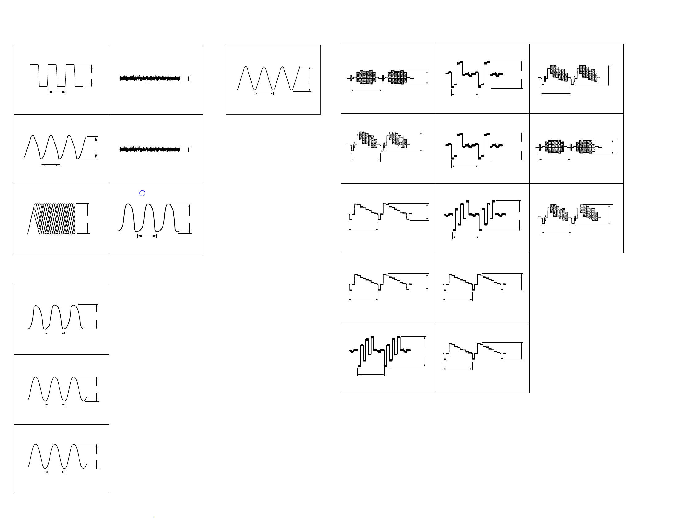
For Schematic Diagrams.
Note:
• All capacitors are in µF unless otherwise noted. (p: pF)
50 V or less are not indicated except for electrolytics and
tantalums.
• All resistors are in Ω and 1/
specified.
•%: indicates tolerance.
• f : internal component.
• 2 : nonflammable resistor.
• 5 : fusible resistor.
Note:
The components identified by mark 0 or dotted line
with mark 0 are critical for safety .
Replace only with part number specified.
• C : panel designation.
• A : B+ Line.
• B : B– Line.
•Voltages and waveforms are dc with respect to ground under no-signal (detuned) conditions.
DMB16 and VIDEO boards
no mark : DVD PLAY
Other board
no mark : TUNER (FM/AM)
( ) : DVD PLAY
< > : TAPE PLAY
[ ] : TAPE REC
* : Impossible to measure
•Voltages are taken with a VOM (Input impedance 10 MΩ).
Voltage variations may be noted due to normal production
tolerances.
•Waveforms are taken with a oscilloscope.
Voltage variations may be noted due to normal production
tolerances.
• Circled numbers refer to waveforms.
• Signal path.
F : AUDIO
e : TUNER
k : TAPE PLA Y (DECK A)
d : T APE PLAY (DECK B)
G : REC (DECK B)
J : CD PLAY
N : MIC
c : DVD PLAY
L : VIDEO
E : Y
a : CHROMA
r : COMPONENT VIDEO
q : R, G, B
4
W or less unless otherwise
Note on Printed Wiring Boards.
Note:
• X : parts extracted from the component side.
• : Pattern from the side which enables seeing.
(The other layers' patterns are not indicated.)
Caution:
Pattern face side: Parts on the pattern face side seen from
(SIDE A) the pattern face are indicated.
Parts face side: Parts on the parts face side seen from
(SIDE B) the parts face are indicated.
• Indication of transistor.
C
Q
B
E
Q
B
CE
Q
B
CE
• Abbreviation
E3 : 240V AC Area in E model
E12 : 220V-240V AC Area in E model
E15 : Iran model
EA : Saudi Arabia model
MY : Malaysia model
PH : Philippines model
SP : Singapore model
TH : Thai model
These are omitted.
These are omitted.
These are omitted.
• Circuit Boards Location
KARAOKE board
CD-SW board
TRANS board
MOTOR (LD) board
VIDEO board
PA board
SW board
DMB16 board
PRIMARY board
TUNER PACK
EFFECTOR board
SWITCHING POWER
SURROUND board
SENSOR board
MOTOR (TB) boar
DRIVER boar
HCD-GN1100D
PANEL board
FUNCTION board
JOG board
MAIN board
MIC board
2525
Page 26
HCD-GN1100D
•Waveforms
– DMB16 Board –
1
IC301 9
2V/DIV, 0.1 µsec/DIV
2
IC301 0
2V/DIV, 20 nsec/DIV
3
IC102 6
BICK
0.33
MCLK
41 nsec
DVDRFIP
µ
sec
3.3 Vp-p
4.0 Vp-p
4
IC102 ea
0.1V/DIV, 0.5 msec/DIV
5
IC102 es
0.1 V/DIV, 0.5 msec/DIV
6
IC102
FED
TEO
228
XTALO
0.1 Vp-p
0.1 Vp-p
– PANEL Board –
1
IC900 is
1V/DIV, 0.2 µsec/DIV
XO
250nsec
3.1 Vp-p
– VIDEO Board –
1
IC801 2
0.5 V/DIV, 20 µsec/DIV
2
IC801 4
0.5 V/DIV, 20 µsec/DIV
3
IC801 6
CIN
H
CVBSIN
H
YIN
1.0 Vp-p
1.3 Vp-p
6
IC801 qf
0.5 V/DIV, 20 µsec/DIV
7
IC801 qh
1 V/DIV, 20 µsec/DIV
8
IC801 qk
CRIN
H
CROUT
H
CBOUT
0.8 Vp-p
1.5 Vp-p
qa
IC801 wd
1 V/DIV, 20 µsec/DIV
qs
IC801 wh
1 V/DIV, 20 µsec/DIV
qd
IC800 7
CVBSOUT
H
C OUT
H
VOUT
2.6 Vp-p
2.0 Vp-p
0.2V/DIV, 500 nsec/DIV
– MAIN Board –
1
IC401 qa
32 µsec
0.5 V/DIV, 10 µsec/DIV
2
IC401 qd
XC OUT
X-OUT
0.6 Vp-p
1.7 Vp-p
3.3 Vp-p
40 nsec
0.5V/DIV, 20 nsec/DIV
1.1 Vp-p
H
0.5 V/DIV, 20 µsec/DIV
4
IC801 0
0.5 V/DIV, 20 µsec/DIV
5
IC801 qs
0.5 V/DIV, 20 µsec/DIV
CYIN
H
CBIN
H
1.6 Vp-p
1.6 Vp-p
0.8 Vp-p
H
1 V/DIV, 20
9
1 V/DIV, 20 µsec/DIV
0
1 V/DIV, 20
IC801 w;
H
IC801 wa
H
µ
sec/DIV
CYOUT
YOUT
µ
sec/DIV
1.5 Vp-p
2.0 Vp-p
2.0 Vp-p
H
1 V/DIV, 20
µ
sec/DIV
2.6 Vp-p
200 nsec
1V/DIV, 50 nsec/DIV
3
CN503 2
20V/DIV, 5 µsec/DIV
E-HOT
11 µsec
HCD-GN1100D
60 Vp-p
2626
Page 27
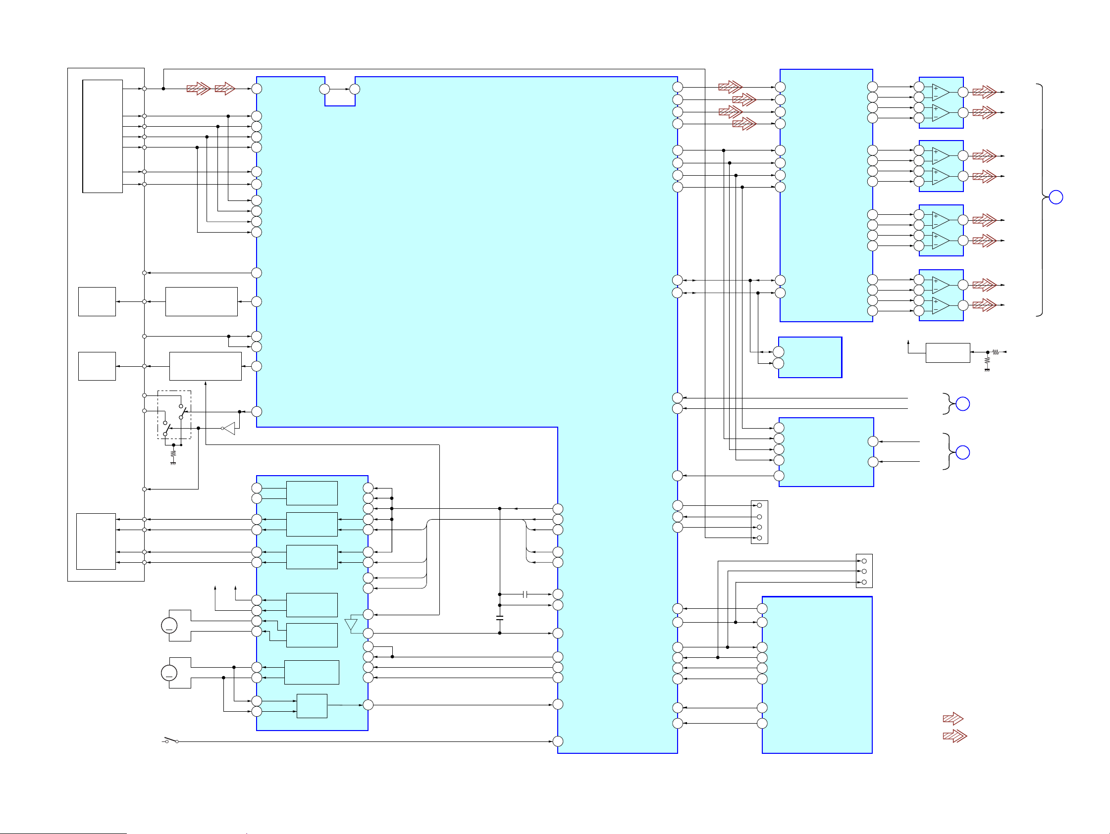
7-1. BLOCK DIAGRAM – RF SECTION –
RF
A
CD LD
PD
DVD LD
WR650
VR780
MSW
FCS+
FCS–
TRK+
TRK–
(SPINDLE)
B
C
D
F
E
VC
M2
(SLED)
M1
Q102 (1/2)
AUTOMATIC POWER
CONTROL (FOR CD)
Q102 (2/2)
AUTOMATIC POWER
CONTROL (FOR DVD)
Q101
MM
MM
REG02
Q103
NC
NC
REG01
SL–
SL+
SP+
SP–
DETECTOR
OPTICAL PICK-UP
BLOCK
(KHM-313CAB)
LASER
DIODE
(FOR CD)
LASER
DIODE
(FOR DVD)
2AXIS
DEVICE
FOCUS/
TRACKING
COIL
6
2
3
4
5
19
18
8
9
10
11
29
23
20
21
22
50
DVDRFIP
DVDA
DVDB
DVDC
DVDD
TPI
TNI
NA
NB
MC
MD
V2O
LD01
MDI2
MDI1
LD02
MSW
OSP
252 253
OSN
IC201
FOCUS/TRACKING COIL DRIVER,
SPINDLE, SLED MOTOR DRIVER
42
41
36 48
37 1
35 3
34 4
32
31
30
29
27
28
BUFFER
FOCUS COIL
DRIVE
TRACKING COIL
DRIVE
SLED MOTOR
DRIVE
SLED MOTOR
DRIVE
SPINDLE MOTOR
DRIVE
HCD-GN1100D
IC3771
AMP
ASDATA0
ASDATA1
ASDATA2
ASDATQ3
ACLK
ABCK
ALRCK
XRST
217
218
219
222
215
214
213
220
14
SDTI1
15
SDTI2
16
SDTI3
13
SDTI4
10
MCLK
9
BICK
17
LRCK
8
PDN
ROUT4+
IC102 (1/2)
CD/DVD RF AMP,
FOCUS/TRACKING ERROR AMP
DVD SYSTEM PROCESSOR
DIGITAL SERVO PROCESSOR
SDA
103
102
SCL
SMSCK
TXD
RXD
V2 REF0
PRST
IFCK
IFSDO
IFSDI
XIFCS
IFBSY
206
208
209
107
106
28
110
99
98
101
100
105
CN105
1
2
5
6
25
33
32
31
24
23
VOICE/YUV7
SPDATA/SMSDI
9
12
43
10
13
42
40
21
19
20
22
VREFO
FOO
TRO
FMO
DMO
IOP
IOPMON
VREFO
FMO
FOO
DMO
TRO
30
38
42
37
41
245
246
40
211
210
170
VREFO
FMO
FOO
DND
TRO
RFRPDC
RFRPAC
IOPMON
MUTE123
MUTE
TSD M
IC301
CONVERTER
20
SDA
19
CSL
SDA
5
SCL
6
13
PDN
11
MCLK
12
SCLK
10
LRCK
9
SDTO
TXD
RXD
V2REF0
RFMON
MTK-RESET
MTK-SCO
MTK-SOD
MTK-SIO
MTK-XIFCS
MTK-BUSY
D/A
IC103
EEPROM
IC3601
D/A
CONVERTER
(FOR CHECK)
ROUT3+
ROUT2+
LOUT4+
LOUT4-
ROUT4-
LOUT1+
LOUT1ROUT1+
ROUT1-
LOUT3+
LOUT3-
ROUT3-
LOUT2+
LOUT2-
ROUT2-
AINR
AINL
CN402
38
37
33
32
2
1
48
47
42
41
40
39
46
45
44
43
(IC3711,3731,3751,3771)
1
2
(1/3)
TXD1
RXD1
CLK1
3
2
5
6
IC3711
3
2
5
6
IC3751
3
2
5
6
IC3731
3
2
5
6
BIAS
XVOICE
SCORE
RIN
LIN
(FOR CHECK)
AMP
AMP
AMP
Q3801
BIAS
B
F
1
7
1
7
1
7
1
7
MAIN
SECTION
(Page 30)
MAIN
SECTION
(Page 30)
DM_L
DM_R
MB_FL
MB_FR
FC
SW(LEE)
MB_SL
MB_SR
AU+5V
A
MAIN
SECTION
(Page 30)
HCD-GN1100D
S1
(LIMIT)
46
47
BUFFER
45
176
47
SPFG
LIMSW
MIC/VSYNC
KRMOD/HSYNC
205
207
21
MIC STATUS
22
MTK-KRMOD
IC401 (1/6)
SYSTEM
CONTROLLER
• Signal Path
: CD PLAY
: DVD PLAY
2727
Page 28
HCD-GN1100D
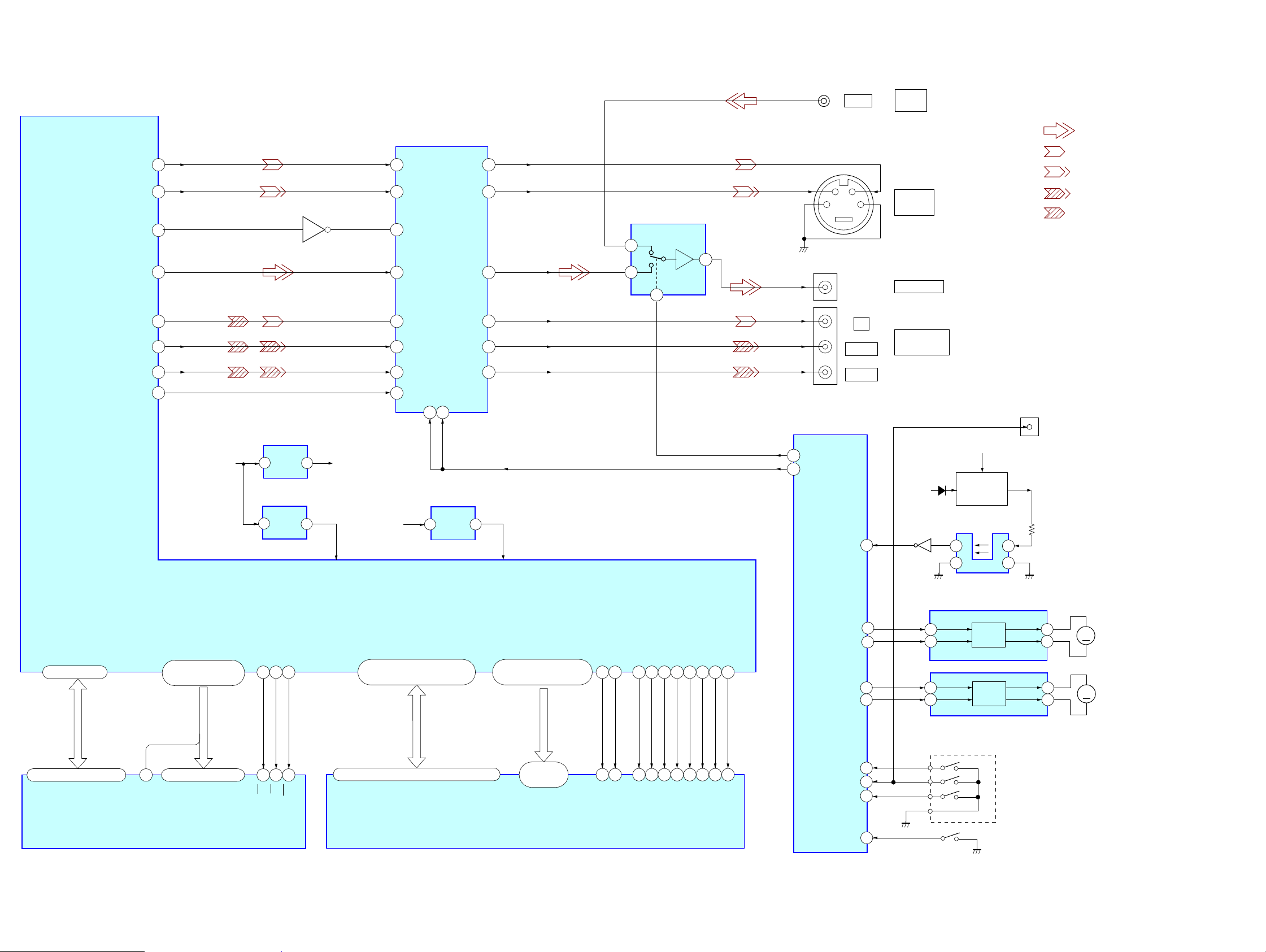
7-2. BLOCK DIAGRAM – VIDEO SECTION –
YUV1
YUV2
DISC/X
YUY3
YUY4
YUY5
YUV6
WODE
194
196
168
198
200
202
203
49
SW+5V
IC107
5
5
+3.3V
REG.
IC105
+3.3V
REG.
Q800
4
4
+3.3V
RF+3.3V
VDD
VIDEO AMP, 75 OHM DRIVER
6
YIN
2
CIN
I/P
9
4
CVBSIN
10
CYIN
12
CBIN
14
CRIN
25
SI
MUTE1
MUTE2
3 13
IC106
+1.8V
IC801
SW+3.3V
1 3
REG.
YOUT
COUT
VOUT
CYOUT
CBOUT
CROUT
21
26
23
20
18
16
AV SEL1
RF1.8V
DVDD18
VOUT
CYOUT
CBOUT
CROUT
IC800
VIDEO SELECT
3
1
2
7
VIDEO OUT SW
V MUTE
J1102(1/2)
J801
C
J802
J800
IC401(2/6)
SYSTEM CONTROL
87
VIDEO-OUT-SW
VIDEO MUTE
88
TBL SENS
VIDEO
21
Y
PB/C
PR/C
VIDEO
INPUT
• Signal Path
: VIDEO
: Y
: CHROMA
Y
S VIDEO
43
OUT
VIDEO OUT
COMPONENT
VIDEO OUT
B
R
CN402
(2/3)
RTS1
M+9V
D505
EVER 4V
+3.3V
REG.
Q523,524
D+3.3V
: COMPONENT VIDEO
: R, G, B
(FOR CHECK)
IC731
Q731
27
TABLE SENSOR
3
4
1
2
HIGHA0-7
IOA0-7, IOA18-IOA20
AD0 – AD7
81-84,86-88,91
A16, A17
53-61, 67-72, 74-76,
78, 89, 92, 93
A0 – A21
HD0 – HD7
A0
A1-A21
29,31,33,35,38,40,42,44 25-16, 10-1, 40,12,48
DQ0 – DQ7
A0 – A21DQ15/A-1
IC101
FLASH ROM
HCD-GN1100D
IC102(2/2)
DVD SYSTEM PROCESSOR
IOCS
IOWA
IOOE
77
79
66
2645
28OE11
CE
WE
RD0 – RD15
125-123, 121, 120, 118,
117, 115, 135, 133-128, 126
2,4,5,7,8,10,11,13,42,44,45,47,48,50,51,53
RD0 – RD15
RA0 – RA11
146, 147, 149-151,
158-160, 162, 164-166
22-26,
29-35
RA0 – RA11
IC104
SDRAM
RCLK
RCS
RWE
RAS
16
140
18
RWE
139
17
RAS
CAS
CAS
BA0
BA1
142
143
145 156 113 137 157
20
21
BS0
BS1
138
38
19
RCS
DRCLK
2828
15
DQM0
DQM1
39
DQM0
DQM1
IC701
LD MOTOR DRIVER
LM-F
LM-R
38
39
FIN
7
RIN
9
MOTOR
DRIVE
OUT2
OUT1
2
4
M
M751
(TABLE LOADING)
CLE
TM-F
TM-R
FIN
36
37
7
RIN
9
MOTOR
DRIVE
OUT2
OUT1
2
4
M
M741
(TABLE)
IC712
TBL MOTOR DRIVER
E-1
37
CKE
OPENSW
E-2
E-3
35
34
28
26
S711
ROTARY
ENCODER
S751
(OPEN)
Page 29
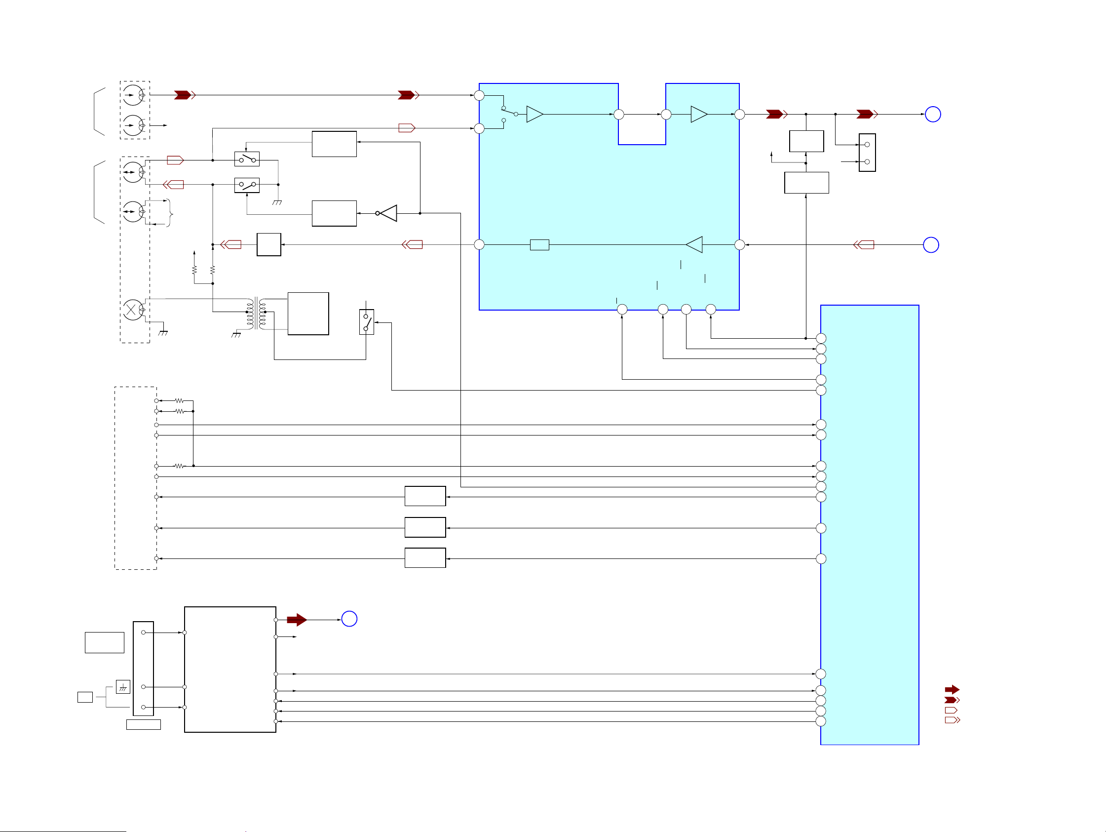
7-3. BLOCK DIAGRAM – TAPE/TUNER SECTION –
DECK-A
L – CH
PB
HEAD
R – CH
DECK-B
L – CH
REC/PB
HEAD
R – CH
R-CH
Q325, Q375
Q321, 322
R-CH
SWITCH
DRIVE
Q382, 383
SWITCH
DRIVE
Q377, 379
Q381
HCD-GN1100D
AIN1
32
A
B
34
BIN1
EQ OUT1
28 27 26
DECK A/B SELECT
PB/REC EQUALIZER AMP
IC301
TAI1
PB OUT1
R-CH
MUTE
Q106
MUTE DRIVE
Q509, 510
R-CH
CN510
TC-PB-L
L
TEST
CONNECTOR
R
C
MAIN
SECTION
(Page 30)
ERASE
HEAD
TAPE
MECHANISM
BLOCK
REC(REV)
REC(FWD)
B PULSE
A PULSE
BHALF
AHALF
ATRGM+
BTRGM+
CAP M+
CN509
R-CH
T301
BIAS
TRAP
BIAS OSC
Q370
BIAS+9V
Q378,380
Q340, 343
A TRIG
DRIVE
Q342, 345
B TRIG
DRIVE
Q341,344
CAP MOTOR
DRIVE
REC-OUT1
21
EQ
A/B
13 11 15 14
ALC ON/OFF
REC MUTE ON/OFF
REC IN1
MUTE ON/OFF
24
SYSTEM CONTROL
(DVD/TAPE MECHANISM CONTROL)
REC-OUT-L
D
MAIN
SECTION
(Page 30)
IC401(3/6)
71
TC-MUTE
54
REC-MUTE
56
ALC
55
PB-A/B
REC BIAS
52
90
B-SHUT
A-SHUT
89
B-HALF
91
A-HALF
47
53
TC-RELAY
48
A-TRIG
49
B-TRIG
CAPM-CONT
50
AM
HCD-GN1100D
FM 75
COAXIAL
ANTENNA
FM/AM TUNER UNIT
FM ANT
AM ANT
ST-DIN/MC-DOUT
AM ANT
ST-L
ST-R
TUNED
ST-DOUT
ST-CLK
ST-CE
R-CH
ST-L
E
MAIN
SECTION
(Page 30)
TUNED
1
ST-DOUT
2
MC-DIN (ST)
5
3
ST-CLK
ST-CE
6
• R-CH is omitted due to same as L-CH.
• Signal Path
: TUNER
: TAPE PLAY (DECK A)
: TAPE PLAY (DECK B)
: RECORD (DECK B)
2929
Page 30
HCD-GN1100D
7-4. BLOCK DIAGRAM – MAIN SECTION –
RF
SECTION
(Page 27)
IC1101
SCL/ECHO VOL
RV1501
ECHO
LEVEL
MIC DETECT
DIGITAL ECHO
16
37
40
41
2
13
6
10
15
14
DATA CLOCK
I/F
17 18
81 82
VOL IC DATA
MIC VOL IN
MIC OUT
+
VOL IC CLK
8
28
R-CH
38
39
R-CH
34
32
R-CH
12
5
9
24
R-CH
IC401(4/6)
SYSTEM CONTROL
MIC OUT
IC304 (1/2)
MUSIC L+R
21
+
INPUT SELECT SWITCH,
GRAPHIC EQUALIZER CONTROL,
ELECTRICAL VOLUME
SAT-L
4
DVD1
INPUT
5
TC-L
SELECT
3
ST-L
SWITCH
6
VIDEO-L
7
R-CH
SUR-L
42
11
4
3
8
7
23
AMP
IC101
LPF
J1100(3/3)
J1150(3/3)
+
+
SURROUND
VOL CONTROL
IC201
2
MIC
IC1100
MIC AMP
J1100(1/3)
MIC 2
J1150(1/3)
MIC 1
IC1500
MIXER
DM-L
+
1
3
A
DM-R
MB_FL
MB_FR
FC
MB_SL
MB_SR
SW (LFE)
2
3
IC1503
MULTIPLEXER
IC1501
DIGITAL DELAY
LPF1OUT
19
LPF2OUTLPF1IN
OP2OUT
A
CLOCK
14
3
COM
AB
C
10 911
44
EFFECTOR S143EFFECTOR S2
EFFECTOR S0
LPF2IN
OP2IN
9
+
10
11
12
Q1500
Q1502
3
5
J1100(2/3)
J1150(2/3)
TAPE/TUNER
SECTION
(Page 29)
TAPE/TUNER
SECTION
(Page 29)
Q1508
BUFFER
Q1509
57 70
EFFECTOR-CTR1
Q1506
TC-PB-L
C
ST-L
E
BUFFER
Q1513
1
7
TV/SAT
AUDIO
AUDIO
IC1505
MIXER L/R
5
3
EFFECTOR-CTR3
VIDEO
INPUT
RV1150
MIC 2
LEVEL
RV1100
MIC 1
LEVEL
J201
L
IN
R
L
R
J1102(2/2)
7
13
MIC AMP
3
5
R-CH
R-CH
IC1506
SELECTOR CCT
1
0Y
12
OX
11
3X
18
IC1102
34
Y COM3Y
13
X COM
BA
9 10
EFFECTOR SELECT
5
1
7
DM_L
DM_R
MB_FL
MB_FR
FC
MB_SL
MB_SR
SW (LFE)
MIC IN
MUTE
Q200,202-204,
250,252-254
MUTE DRIVE
Q507,508
77 85 79 80
DVD A MUTE
8
RECB1
SURROUND OR
DPL BUFFER
IC2000
MIC/MUSIC AMP
31
57
25
31
30
29
28
27
26
22
IC2001
COMPARATOR
3
1
2
5
D2004
-2008
C
A
B
C
A
B
MID/
BASS &
TREBLE
R-CH
SAOUT
+
7
6
IC2002
COMPARATOR
31
67
LINK-L
TOUT1
14 15
19
COMMAND
MUTE DRIVE
Q505,506
VOLIN1
VOLUME
CONTROL
SCORE
XVOICE
CPU
INTERFACE
DATA
RF
SECTION
B
(Page 27)
REC-OUT-L
R-CH
+
CLK
22 1621
46
8376
BB-A1
SWOUT
24
OUT1
18
BB-B1
17
Q101
A+9V
R-CH
R-CH
MUTE
Q514, 564
MUTE DRIVE
Q511
75
MUTE DRIVE
Q519,512,515
R-CH
AC DETECT
TAPE/TUNER
D
SECTION
A +9V
IC304 (2/2)
SPEANA IN
6
J
(Page 29)
4V REG.
Q323
AMP
7
DISPLAY/POWER
SECTION
(Page 32)
R-CH
MUTE
Q117
MUTE DRIVE
Q516, 517
MUTE
Q206
MUTE DRIVE
Q521, 522
R-CH
D +4V
L+R
(SPEANA)
SPEANA
DBFB F/B
F-R
F-L
LINE-MUTE
CENTER
SL
SR
SW OUT
J202
L
R
LIN
RIN
F
J103
DISPLAY/POWER
G
SECTION
I
(Page 31)
H
• R-CH is omitted due to same as L-CH.
AUDIO OUT
SECTION
(Page 27)
D-LIGHT
SYNC
OUT
SECTION
(Page 32)
AMP
AMP
SECTION
(Page 31)
RF
• Signal Path
LINE MUTE
AUDIO IC CLK
AUDIO IC DATA
ANALOG IN MUTE
AUDIO-OUT-MUTE
SW MUTE
: AUDIO
: TUNER
: DVD PLAY
: TAPE PLAY
: REC (DECK B)
: MIC
HCD-GN1100D
3030
Page 31

7-5. BLOCK DIAGRAM – AMP SECTION –
HCD-GN1100D
F-R
MAIN
SECTION
(Page 30)
IC600
POWER AMP
F-L
STK MUTE
18 11
14
Q604, 606, 610
CT
4
OUT
3
10
12
MUTING
IC550
OVER CURRENT
PROTECTOR
8
9
DC DET
OVER
LOAD
TH629
VP
OCP
+ +
THERMAL
DETECT
Q628, 630
2
1
I
D550
DBFB F/B
OVER LOAD
DETECT
Q668, 618
D624
MUTING
Q640, 641
MUTING
CONTROL
Q634,682
HP-MUTE
RY646
RELAY DRIVE
Q644, 647
F-RELAY
FAN CONTROL
SWITCH
Q578
Q648
HI SPEED
SWITCH
Q581, 582
+
FAN CONTROL
H/P DET
FAN DET
HI SPEED
FAN MOTOR
DRIVE
Q587 - 589
FAN MOTOR
DRIVE
Q579, 585
TM600
+
-
+
-
L
R
M
M
J1103
PHONES
FRONT SPEAKER
M892
DC FAN
M891
DC FAN
MAIN
SECTION
(Page 30)
H
IC800
POWER AMP
Q730, 770. 780, 800, 850
SW OUT
SL
SR
CENTER
LINEMUTE
SW MUTE
Q812
MUTE
Q810
MUTE
Q750
MUTE
Q700
MUTE
Q740
13
14
11
POWER AMP
18
6
7
4
5
IC801
+
11
10
+
14
19
8
9
21
22
D812
OVER LOAD
DETECT
RELAY DRIVE
Q814, 815
RELAY DRIVE
Q763
RELAY DRIVE
Q762
RY862
RY760
RY761
D780
D765
-
+
TM700
+
-
+
-
+
-
TM701
VL(AC)
K
TM101
SUB WOOFER
L
SPEAKER
R
CENTER
SPEAKER
DISPLAY/POWER
SECTION
(Page 32)
OUT
REAR
HCD-GN1100D
STK MUTE
60 67
STK-MUTE
PROTECTOR
IC401 (5/6)
SYSTEM CONTROLLER
61
51
SURR-RELAY
SW-SPK RELAY
65
CENTER-RELAY
HP-DET
F-RELAY
HP-MUTE
42
FAN-CONTROL
58
FAN HI SPEED
72
HP-MUTE
66 84
HP-DETECT
FRONT-RELAY
• SIGNAL PATH
: AUDIO
3131
Page 32

HCD-GN1100D
7-6. BLOCK DIAGRAM – DISPLAY/POWER SECTION –
MAIN
SECTION
(Page 30)
Q902
LED+9V
Q903
D906, 908, 910, 913, 915, 917,
919, 921, 929, 923, 925, 927
+VL
–VL
+VH
–VH
– VG
(-32V)
TO FLUORESCENT
INDICATOR TUBE
D672
RECT
D658
RECT
D656
– 33V
REGULATOR
Q1264
FL901
RECT
D560
F1261
F1271
F1241
F1251
VF1
VF2
R1292
F1281
TRANSFORMER
VL
VL
GND
VH
VH
VP
D1292
RECT
VF
VF
AC3
AC3
T1200
POWER
VL(AC)
X
K
UNREG
EXCEPT TH
AMP
SECTION
(Page 31)
VOLTAGE
CHECK
Q504, 550
M +9V
LED +9V
A +9V
ST +9V
BIAS +9V
R480
IC561
+9V REG
IC560
+9V REG
SW +9V
68OVER VOLTAGE DET
AU +5V
+5V REG.
Q103
AUDIO +9V
LED SELECTOR
IC900
KEY2
|
KEY0
64 – 66
80
52– 59,
75,76,78,79
60I2C DATA
61I2C CLK
77RESET
S900 – 905, 907 - 914,
916 - 928, 934, 937
Q900
LED DRIVE
Q906-916, 921
30 IIC-DATA
29 IIC-CLK
40 GC-RESET
NO.402
IIC-DATA
IIC-CLK
IC401 (6/6)
SYSTEM CONTROL
Q901
D905, 907, 909, 912, 914,
916, 918, 922, 924, 926
(FOR CHECK)
X900
4MHz
P1 – 36
ND900
FLUORESCENT
INDICATOR TUBE
VF1
VF2
-VG
(-32V)
SPEANA
X
G
D900
OPERATION
2
1
DIAL
MASTER
VOLUME
G1,22,23
G2-21
IC902
SPECTRUM
ANALYZER
IN2
IN1
Q917, 918, 919
ROTARY
ENCODER
S936
ROTARY
ENCODER
S935
BUFFER
16
15
14
13
17
83 XIN
82 XOUT
P1 – 36
9, 10, 12 – 22,
24 – 41, 43 – 47
DISPLAY CONTROL,
KEY CONTROL
G1,22,23
7, 8, 86
G2 – 21
1 – 6, 87-100
48
VKK
68
BF4
69
BF3
BF2
70
BF1
71
ALL BAND
67
72 OPERATION DIAL
74 VOLUME
D904
(R)
D930
(G)
LED DRIVE
Q904,905
S934
S900
DISPLAY
IC901
REMOTE CONTROL
RECEIVER
X402
5MHz
X401
32.768kHz
41 STBY-LED
74 POWER-KEY
73 DISPLAY-KEY
4 SIRCS
15 X-IN
13 X-OUT
10 XC-IN
11 XC-OUT
IC559
+3.3V REG
IC558
+5V REG
M+9V
EVER +4V
D501
IC507
+9V REG
D505
+B SWITCH
Q513,520
MAIN
SECTION
(Page 30)
X
J
POWER
SWITCHING
AC CUT
DETECT
RECT
D561
D506
POWER ON/OFF
RELAY DRIVE
Q1200
F1291
AC4
AC4
RY1200
EXCEPT TH
TH
S1200
S1200
VOLTAGE
SELECTOR
230 – 240V
|
220V
|
120V
AC IN
MB +9V
REG. SWITCH
Q104
CN402
(3/3)
RESET
SWITCH
Q501
REG. SWITCH
Q518, 503
RESET
+SW3.3V
V +5V
AU+5V
+SW5V
(ZIVA)
D3.3V
(FOR CHECK)
IC501
1 2
LEVEL
DETECT
B+ SWITCH
Q523, 524
78MTK-POWER
7STBY-RELAY
12RESET
20AC-CUT
HCD-GN1100D
3232
Page 33

7-7. PRINTED WIRING BOARD – DMB16 BOARD (SIDE A) –
HCD-GN1100D
Ver. 1.1
• See page 25 for Circuit Boards Location. :Uses unleaded solder.
1
A
DMB16 BOARD (SIDE A)
2
B
C
R121
R118
R120
E2
C2
B1
B2
Q102
C1
E1
Q101
C106
FL101
D2
G1
S1
1
5
25
R116
R108
Q103
E
CN107
24
R107
R109
R1161
R1109
2
6
R1129
1
224
OPTICAL
PICK-UP
BLOCK
D
(KHM–313CAB)
CN101
23
C101
G2
R117
R101
S2
D1
E
C221
F
IC201
36
37
C212
G
3 4 5 6 7 8
IC3771
C3702
R126
C214
IC107
C192
C114
R225
R3779
C124
C3772
C3752
C132
R136
C130
C3774
R3776
C3754
R3756
R3508
1
1
45
R3782
R3781
R3759
1
45
IC3751
R3507
C137
C135
C138
C133
R3784
C3781
C3704
R3788
R3789
8
R3787
C3784
C3782
R3783
R3786
R3769
8
C3764
R3766
R3764
R142
R3768
R3767
C3762
R143
R3762
R1168
R3763
R1540
R1547
C153
R3761
C3761
R146
R1561
R314
R151
R1531
R1543
R153
C301
R155
R160
R1530
EXCEPT EA
193256
192
C305
1
IC301
12
13
FB1502
R1526
FB1501
EAEA
R1524
EXCEPT EA
R1542
R1553
C170
3748
24
R1101
36
C302
25
C309
R319
EA
R3801
FL107
27
R3718
R3717
R3737
R3738
C3802
C3712
C3734
C3732
R3802
R3803
IC3711
R3719
C3714
1
45
R3716
R3722
R3721
R3739
1
45
R3736
R3742
R3741
Q3801
E
R3804
R3805
C3708
8
R3724
C3721
C3706
8
R3744
C3741
IC3731
R3778
R3777
R3758
R3757
C193
C195
IC102
IC104
RB104
RB103
RB111
64
R127
R219
13
12
1
48
R223
R212
65 128
R1557
R152
1
FL105
24
IC101
C108
R1544
R161
R131
48
25
RB112
C102
C109
129
RB113
FL106
RB108
RB107
FL104
FL108
RB105 RB106
154
5
IC106
1
D1001
IC105
R187
C188
SP, MY, TH, PH
R3729
C3724
R3726
C3744
R3746
R5001
R5016E3, E12, E15, EA
R5017
EXCEPTEAEA
R3504 FB3504
EXCEPT
EA
R3728
R3727
C3722
R3723
R3749
R3748
R3747
C3742
R3743
FL401
R1139
R1138
R3505
L3602
C189
FB3503
EA
R3606
R3609
R3610
FB403
FL403
C3605
C3603
IC3601
8
9
R3607
R3608
1
16
R3605
C3607
D3601
R4509
FB401
FB405
1-871-691-
R3611
R3631
FL402
R3621
R3602
12
(12)21(21)
• Semiconductor
Location
Ref. No.
D1001 E-6
D3601 C-7
IC101 F-4
IC102 D-4
IC104 E-5
IC105 F-6
IC106 E-6
IC107 C-3
IC201 F-3
IC301 B-5
IC3601 C-7
IC3711 B-6
IC3731 C-6
IC3751 B-4
IC3771 B-4
Q101 D-2
Q102 C-2
Q103 D-2
Q3801 C-6
Location
HCD-GN1100D
3333
Page 34

HCD-GN1100D
Ver. 1.1
7-8. PRINTED WIRING BOARD – DMB16 BOARD (SIDE B) –
• See page 25 for Circuit Boards Location. :Uses unleaded solder.
1
2
DMB16 BOARD (SIDE B)
3 4 5 6 7 8
C
MAIN
BOARD
CN521
(Page 41)
B
VIDEO
BOARD
CN801
(Page 58)
A
EA
C308
R3633
C3601
C3604
C3804
D3501
C3723
R3725
C3743
R3745
C3803
ET002
C3606
B
R3601
D3602
C3602
R3604
C
D
15
FB402
C402
C403
FB404
FB406
E
MAIN
BOARD
NO523
(Page 41)
D
CN401
F
ET001
G
C3805
2
1
C3713
R3715
C3701
R3733
C3733
C3703
C187
C184
C182
R1134
CN315
R3713
R3711
R3712
C3711
R3714
C307
R3731
R3732
C3731
R3734R3735
C3801
C181
C190
C179 C180
R169
R1133
R1110
CN105
16
(FOR TEST)
R3636
R3635
R3634
20
21
R1102
C178
R196
C177
C111EAC110
EA
R3652
R3653
R1124
R1125
R189
R190
C191
R1502
FB115
1
2
R3506
R1123
R1122
R192
R195
C163
R1105
C164
CN109
R1121
R197
A
R1120
R1559
C171
C172
C173
C174
C175
FB113
FB114
BOARD
(Page 41)
R1551
C161
C159
C176
C160
FB112
MAIN
CN520
C306
R1550
R1548
R1549
R1104
C162
R1504
12
13
R1527
R1103
C158
R164
C167
FB111
R1546
R3651
C154
C156
C155
R191
R193
8
1
IC103
R141
C146
R1151
R1150
5
4
CN202
C3783
R3785
C3763
R3765
C152
C139
C151
R1152
C144
R106
C149
C148
R104
C3773
R3775
C3707
C3753
R3755
C3705
X101
R138
C140
C125
C147
C126
R1126
R1554
C127
C136
R105
5
4
(FOR TEST)
R3773
R3753
C196
C128
R1171
1
2
R3754
C131
C3771
R3772
R3774
C3751
C123
C116
R214
C205
R3751
R3752
C150
C122
C115
C129
R210
R208
R3771
C121
C119
C210
R207
R204
C203
R209
C120
C208
C206
R224
R216
R215
R220
R4704
C118
C117
C233
R206
C209
2
1
R4705
R123
C213
R2504
R213
R205
R221
R226
C211
R4706
R231
CN302
C112
C113
R230
R234
R232
R233
R4702
R4703
R124
R115
R114
R111
R247
R246
C215
C217
12
13
R4701
R113
R321
R112
C105
R110
CN103
1
5
6
CN201
1
C222
C219
C218
C224
1-871-691-
2
4
ET003
C220
(FOR TEST)
(KHM–313CAB)
12
(12)21(21)
OPTICAL
PICK-UP
BLOCK
• Semiconductor
Location
Ref. No.
D3501 B-2
D3602 B-2
IC103 F-5
Location
HCD-GN1100D
3434
Page 35

7-9. SCHEMATIC DIAGRAM – DMB16 BOARD (1/4) –
16
DMB16
BOARD
(Page 36)
(Page 37)
(Page 38)
DMB16
BOARD
(2/4)
(Page 36)
(Page 37)
DMB16
BOARD
(2/4)
(Page 36)
(3/4)
(Page 37)
(4/4)
(Page 38)
(2/4)
(3/4)
(4/4)
DMB16
BOARD
(3/4)
(Page 36)
DMB16
BOARD
(2/4)
(Page 36)
DMB16
BOARD
(2/4)
19
15
GND
SPDATA
SW+5V
ABCK
ACLK
ASDATA0
ASDATA1
ASDATA2
ALRCK
SCL
SDA
XRST
ASDATA4
D3601
100R3606
0
R3635
R3651
EXCEPT EA
MC2837
0
R3634
0
C3607
0.01
R3610
EA
R3603
10k
100
0
R3636
R3801
FERRITE
BEAD
C3801
10V
0R3607
0R3608
0R3609
0
100
R3653
R3652
0
AK5358AET-E2
R3602
0
10k
R3605
10k
0
C305
0.47
C306
100
10V
R3802
R3604
0
CSK0
161514131211109
3.3
CSK2
10k
DIF
0
PDN
3.2
SCLK
1.6
MCLK
1.6
LRCK
1.6
1.2
R3804
18k
• See page 26 for Waveforms. • See page 64 for IC Block Diagrams. • See page 72 for IC Pin Function Description.
0
R3621
R3611
IC3601
AINR
AINL
CSK1
VCOM
AGND
DGNDSDTO
R3631
0
R314
100
IC301
AK4358VQ-L
R3803
10k
C3802
0
2.4
2.4
0
C3605
2.4
0.1
4.9
VA
C3603
3.2
C309
0.1
C301
0.01
ART-
87654321
EA
ART+
0.1
C3601
0.1
R319
R3805
VD
10
C3602
10
50V
LOUT1-
LOUT1+
FERRITE BEAD
Q3801
2SC2712-YG
BIAS
1k
C3606
10
50V
C3604
47
35V
C302
0.47
0
0R3601
EXCEPT EA
EA
C3805
47
16V
C3803
100
10V
L3602
10uH
R3633
100
D3602
UDZW-TE17-3.3B
C307
100
10V
C3804
47
16V
ROUT1+
ROUT1LOUT2+
LOUT2ROUT2+
ROUT2LOUT3+
LOUT3ROUT3+
ROUT3-
ALT+
ALT-
ART-
ART+
ALT+
ALT-
ROUT3-
ROUT3+
LOUT3+
LOUT3-
ROUT2-
ROUT2+
LOUT2+
LOUT2-
ROUT1-
ROUT1+
LOUT1+
LOUT1-
R3782
1.5k
0.0018
R3781
R3772
C3771
R3771
R3752
1.5k
R3751
1.5k
R3732
1.5k
R3731
1.5k
R3712
1.5k
R3711
1.5k
1.5k
1.5k
1.5k
R3741
1.5k
R3742
1.5k
R3721
1.5k
R3722
1.5k
C3781
0.0018
R3774
3.9k
R3773
3.9k
R3762
1.5k
C3751
0.0018
C3741
0.0018
C3731
0.0018
C3711
0.0018
R3754
3.9k
R3753
3.9k
R3734
R3733
R3714
R3713
R3784
3.9k
0.0022
R3761
1.5k
3.9k
3.9k
3.9k
3.9k
C3772
R3743
3.9k
R3744
3.9k
C3721
0.0018
R3783
3.9k
R3763
3.9k
0.0018
R3764
3.9k
C3752
0.0022
C3732
0.0022
R3723
3.9k
R3724
3.9k
R3785
4.7k
C3707
0.1
R3775
4.7k
C3761
C3705
0.1
R3755
4.7k
R3745
4.7k
C3703
0.1
R3735
R3725
C3701
0.1
C3712
0.0022
0.0022
4.7k
4.7k
C3782
C3783
R3765
4.7k
R3715
4.7k
330p
C3773
330p
C3753
330p
0.0022
C3742
0.0022
C3743
C3713
C3762
C3763
330p
330p
C3733
330p
C3722
0.0022
C3723
330p
R3786
1k
C3708
R3776
R3756
330p
1k
R3777
R3757
1k
R3737
1k
R3717
R3788
4.7k
IC3771
NJM3414AV
DM L/R AMP
C3774
330p
1k
C3744
330p
C3724
330p
C3764
330p
C3754
330p
C3734
330p
C3714
330p
R3778
4.7k
R3768
4.7k
IC3751
NJM3414AV
C/SB AMP
R3758
4.7k
R3748
4.7k
IC3731
NJM3414AV
SURR L/R AMP
R3738
4.7k
R3728
4.7k
IC3711
NJM3414AV
FRONT L/R AMP
R3718
4.7k
R3759
1k
R3749
1k
R3729
1k
1k
R3767
1k
1k
1k
R3787
C3784
330p
0.1
1k
R3766
1k
1k
R3747
R3746
1k
R3736
1k
R3727
R3726
1k
R3716
1k
R3789
R3779
R3769
1k
R3739
1k
R3719
1k
HCD-GN1100D
Ver. 1.1
RT
1k
1k
LT
SW
C3706
0.1
RT
LT
SW
FC
SR
SL
FR
FL
EA
FB3504
D3501
MC2387
C308
R3504
0
EXCEPT
EA
ET002
CN315
FB3505
R3508
100
R3507
100
21P
RT
LT
(LFE)
MAIN
BOARD
(3/5)
CN521
(Page 44)
XVOICE
2
SCORE
1
EA
SCORE
20
XVOICE
DMB16
BOARD
(2/4)
(Page 36)
R3506
0
0.1
EA
R3505
0
C3704
0.1
C3702
0.1
FC
SR
SL
FR
FL
HCD-GN1100D
3535
Page 36

HCD-GN1100D
Ver. 1.1
7-10. SCHEMATIC DIAGRAM – DMB16 BOARD (2/4) –
• See page 26 for Waveforms. • See page 65 for IC Pin Function Description.
(1/4)
(Page 35)
(Pagge 38)
DMB16 BOARD
(3/4)
(Page 37)
(3/4)
(Page 37)
(4/4)
(Pagge 38)
(4/4)
DMB16
BOARD
(4/4)
(Page 38)
(Page 37)
(Page 38)
DMB16
BOARD
DMB16
BOARD
(4/4)
(Page 38)
DMB16
BOARD
(3/4)
DMB16
BOARD
(4/4)
(Page 38)
DMB16
BOARD
(4/4)
(Page 38)
DMB16
BOARD
(Page 38)
DMB16
BOARD
14
21
(4/4)
DMB16 BOARD (1/4)
DMB16
BOARD
(3/4)
(Page 37)
(4/4)
13
5
CN101
24P
1
7
R101
6
8
16
C132C130
0.10.1
R126
0
3.3
1.3
FL101
0UH
C101
0.01
Q101
UM6K1N-TN
0
R108
100
R107
10k
1M
R110
47k
0.1 0.1
R113
R112
22
0.5%
C105
47
16V
R114
C106
100k
0.01
R111
100
22
0.5%
R109
R116
0.1
R115
0.5%
3.2 3.2
R1129
100k
0
C192
TK11133CSCL-G
0.01
1k
R117
0.7
47k
0
22
22
22
120
118
R
R
2.3
2.3
Q102
QST8TR
IC107
3.3
22
R121
2.62.6
10 50V
C115
10 50V
C116
C117
0.1
C118
0.1
DTC124EKA-T146
C112
47
16V
4.9
3.3
C193
C195
0.22
0.22
1
C120
1
C121
1
C122
1
C123
1
C124
C114
0.1
C119
10
50V
Q103
R124
47k
R123
0
C113
0.01
C125
0.1
C126
0.1
C196
0.0047
NC
NC
R1126
R1554
10k
4.7k
R127
100
C127
0.01
SPFG
DSEL
WIDE
MSW
C133
0.1
15k
R136
NC
NC
1.7
1.7
1.7
1.7
1.7
2.1
2.1
2.1
2.1
9
2
2
0.0015
C128
0.1
2p
2
0.1
R138
100k
40
139
C
C1
3
0.1
0.001
0.03
137
135
C
C138
C
0.1
2.6
3.3
3.3
NC
2.8
1.4
NC
NC
1.4
2.1
1.3
1.4
.1
0
6
14
C
C149
0.1
C147
C148
0.047
0.047
NCNCNC
1.3 0 1.4 0.2 1.8
1.4
3.3
0.2
3.3
0
3.3
1.8
2
2
1.7
1.6
2.1
2.3
1.5
2.2
1.2
3.3
3.3
0.6
1
0.5
2.7
1.3 1.3
2
3.3
2.5
2
0
0 1.8
2.1
0
3.3
1.7
0.9
1
1.2
1.5
0
0
3.1
2.1
0
3.3
3.3
p
10
50V
150
52
C
10
C1
141
R
750k
0.5%
0.001
C151
3.3
3.3
2.6
2.7
3.3
3.3
3.2
1.7
3.3
1
1.4
1.5
2.4
(Page 35)
10
z
H
M
27
15p
153
X101
C
30
100k
3
42
68
R1
11
R
470P
4
C15
IC102
CXD9849R
1.8
0.8
1
1.3
0.9
3.3
1.2
1.6
1.3
1.5
1.2
1.2
1.3
1.8
3.1
2.7
3.1
R1547
3
4
T
ATA
S
D
R
S
X
A
R146
56
10
1
C
0.01
4.7k
1540
R
3.3
2.5
1.4
1.6
0
0.7
1.9
2
1.6
1.8
3.3
1.6
1.9
0
0
0
DMB16
BOARD
DMB16
(1/4)
BOARD
2
(Page 35)
k
.7
7
4
47
4
47
47
151
R
4.7k
R1561
47
0
155
153
531
R
1549
16
R
R
R1
R
1550
4.7k
R
548
1
4.7k
R
0
1.4
1.5
1.5
1.6
3.3
NC
3.3
NC
NC
1.8
NC
NC
3.3
4
(1/4)
(Page 35)
7
4
R1527
0
1530
R
4.7k
R1551
0.01
C159
R1559
10k
MUTE
MUTE123
3.3
3.3
1.3
0
3.3
0.7
0
3.3
0.4
DMB16
BOARD
(3/4)
18
(Page 37)
D
O
M
IC
M
KR
1542
10k
R
10k
R1543
1.8
1.2
0
0
3.3
0
0
0
1.8
0
0.6
1.2
0.7
0.7
3.3
1.2
3.3
3.3
0
0.1
1.6
3.3
1.6
0
0
1.6
1.3
0
1.2
3.3
0.6
0
3.2
DMB16
20
BOARD
(1/4)
(Page 35)
SCORE
XVOICE
0.5%
0.5%
2
19
190
189
150
150
R
R
R
C163
0.01
161
C
0.01
NC
NC
NC
NC
NC
NC
NC
NC
REW
NC
FWD
NC
NC
TSD M
NC
NC
3.3
0
0
1.3
0
0
0
0
0
3.3
%
0.5
0.5%
0.5%
0.5%
2
150
150
150
R1120
R1553
0
R110
R1121
0
R1125
0
R1124
0
R1123
0
R1122
0
R1101
2.2k
0
C170
0.01
C171
0.01
0.01
C172
C173
0.01
C175
0.01
0.01
C176
100
RB108
R1103
C174
0.01
R1105
0
R4701
R4702
0
R4703
0
R4704
0
R4705
0
R4706
0
R321
ET003
0
10k
R1104
10k
R1161
10k
RB104
47
RB103
47
RB111
47
R1109
0
0
150
R197
R195
CN302
13P
15
DMB16
BOARD
(1/4) (3/4) (4/4)
(Page 35) (Page 37) (Page 38)
12
11
DMB16
BOARD
(4/4)
(Page 38)
DMB16
BOARD
(4/4)
(Page 38)
B
VIDEO
BOARD
CN801
(Page 59)
HCD-GN1100D
R196
FL105
0UH
C129
C131
10
2.2
50V
C136
0.01
C144
0.01
DMB16
BOARD
16
(3/4)
(Page 37)
C155
0.01
0
152
R
100
R1557
C158
0.01
uH
100
R164
161
100
R
0
C160
0.01
1504
R
RB112
22
RB113
C164
0.01
22
C177
C162
47
0.01
16V
RB107
0
47
FL106
0UH
17
DMB16
BOARD
(3/4)
(Page 37)
3636
Page 37

7-11. SCHEMATIC DIAGRAM – DMB16 BOARD (3/4) –
HCD-GN1100D
Ver. 1.1
A
MAIN
BOARD
(1/5)
CN520
(Page 42)
M-REQ
DGND
KRMOD
16
R106
10k
CN109
13P
MIC
NC
EXCEPT EA EA
R1526
100
CN105
6P
R104
R1524
100
0
R105
10k
IC101
MX29LV320CBTC70-CBA3-0604CE
MX29LV320CBTC70-CBA3-0604GA
0
0.9
0.5
0.6
2.9
1.6
2
1.8
0
0
3.3
3.3
3.3
3.3
0
0
1.3
2.3
2.1
1.6
1.7
2
2
R1171
100
FB1502 FB1501
(E3,E12,E15,EA)
(PH,MY,SP,TH)
2.8
2
1.3
1.2
1.6
1.2
3.3
1
0.9
1.6
0
0
0
0
R1544
0
C108
C109
17
DMB16
BOARD
(2/4)
(Page 36)
R1133
C181
0.001
3.3
TK11133CSCL-G
4.9
C190
47 6.3V
IC105
1.6
2.4
2.5
0.6
0
1.6
1.3
2.5
3.1
2.7
0
0
3.3
1.8
0.9
1
3.3
1
1.5
1.3
1.5
3.3
1.2
3.3
C179
0.1
FL108
0UH
R187
0
RB106
22
C180
0.1
RB105
22
21
DMB16
BOARD
(2/4) (4/4)
(Page 36) (Page 38)
DMB16
BOARD
(1/4) (2/4) (4/4)
(Page 35) (Page 36) (Page 38)
13
1.6
0
1.7
1.4
0
0
0
1.9
1.6
1.2
0.9
3.3
0
0
0.9
0.001
C191
1.4
3.3
0.9
1.3
1.5
IC104
A2V64S40CTP-G75
R169
10k
C184
0.01
0
C182 C188
0.22 0.22
DMB16
BOARD
(2/4)
16
(Page 36)
C102
1
FL104
0UH
R193
R191
1k
R1546
3.3k
IC103
BR24L64F-WE2
1k
C167
0.01
FL107
0UH
C178
47
16V
10
0.001
0.001
C110
100p
C111
100p
EA
FB111
FB112
FB113
FB114
FB115
0UH
R1502
*
FERRITE BEAD
R1502
0
0UH
0UH
0UH
0UH
*
EXCEPT EA
EA
R1150
R1152
3.3k
R1151
3.3k
3.3k
R1134
0
IC106
NJM2387ADL3
R1139
1k
R1138 470
C189
0.33
D1001
RB501V-40TE-17
C187
47
16V
DMB16
BOARD
(2/4)
(Page 36)
DMB16
BOARD
(1/4) (2/4)
(Page 35) (Page 36) (Page 38)
15
(4/4)
HCD-GN1100D
FOR TEST
KRMOD
18
DMB16
BOARD
(2/4)
(Page 36)
2.7k
R1110
7
DMB16
BOARD
(2/4)
MIC
SCL
SDA
(Page 36)
19
DMB16
BOARD
(1/4)
(Page 35)
3737
Page 38

HCD-GN1100D
7-12. SCHEMATIC DIAGRAM – DMB16 BOARD (4/4) –
16
DMB16
BOARD
8
(2/4)
(Page 36)
DMB16
BOARD
(2/4)
(Page 36)
14
DMB16
BOARD
(2/4)
(Page 36)
R231
0.5%
R232
18k
0.5%
R234
15k
2.9
10k
R233
C215
33k
0.01
0.5%
2.9
1.7
9
9
4.3
4.3
CN201
DMB16
BOARD
(2/4)
1
(Page 36)
6P
4.3
4.3
JL205
4.8
C218
C219
0.01
C224
0.01
C220
10
16V
10
50V
C221
0.1
R246
R247
1k
4.7k
11
DMB16
BOARD
(2/4)
(Page 36)
3.5
4.4
4.2
3.3
C222
5.3
3
3.3
3.3
9
3.3
0.1
R225
100k
0.5%
56k
C211
0.033
0.5%
R226
56k
2.1
2.1
0.3
4.9
R230
82k
0.5%
C212
0.01
C214
0.001
1.4
R212
10k
R206
R208
33k
10k
C205
220p
R214
R223
100k
0.5%
R221
0.5%
C209
C233
0.033
0.0047
R220
10k
1.4
1.4
15k
1.4
1.4
1.4
R209
33k
C206
220p
R215
12k
3.3
C203
R207
0.01
2.7k
R204
1.2k
9
R205
10k
3.3
2.2
1.4
1.4
R210
47k
R213
6.8k
0.5%
C208
0.01
R216
12k
1.4
1.4
0
1.4
1.1
IC201
FAN8036L
DMB16 BOARD (2/4)
(Page 36)
DMB16 BOARD (2/4)
(Page 36)
DMB16 BOARD (2/4)
(Page 36)
HCD-GN1100D
MAIN
BOARD
(5/5)
NO523
(Page 46)
12
R219
27k
R224
10k
C210
0.01
R2504
C213
4.7k
0.01
C217
47
16V
6
5
CN401
5P
D
FB402
0UH
FL401
0UH
C402
16V
FB404
0UH
FB403
0UH
47
FL403
0UH
C403
6.3V
47
FB406
0UH
15
FB401
0UH
FL402
EMI
FB405
0UH
ET001
DMB16
BOARD
21
(2/4) (3/4)
(Page 36) (Page 37)
DMB16
BOARD
13
(Page 35) (Page 36) (Page 37)
(2/4)(1/4) (3/4)
(Page 35) (Page 36) (Page 37)
DMB16
BOARD
(2/4)(1/4) (3/4)
3838
Page 39

HCD-GN1100D
7-13. PRINTED WIRING BOARDS – CD MECHANISM BOARDS –
1
2
BOARDSENSOR
A
CN731
IC731
B
C
1
CN741
BOARDMOTOR(TB)
3
M741
(TABLE)
M
1-687-132-
CN742
1-687-134-
• See page 25 for Circuit Boards Location. :Uses unleaded solder.
3 4 5 6 7
BOARDDRIVER
Q731
E
JW707
JW708
CN703
C715
JW706
JW705
R713
D711
R701
R702
2
1
CN705
R751
C752
JW712
12
(12)
CN702
C751
12
(12)
2
1
R733
R732
R734
R735
C737
CN704
C736
C735
JW710
R723
4
JW711
R736
C741
R722
JW709
R721
1
R711
D701
CN701
IC712
1
R712
1
MAIN BOARD
E
(Page 41)
JW704
IC701
JW713
JW714
CN511
JW702
JW703
R731
9
9
C731
JW701
1-866-201-
12
(12)
2
1
CN751
BOARDSW
S751
(OPEN)
1-687-669-
12
(12)
D
E
HCD-GN1100D
BOARDMOTOR(LD)
M
M751
(TABLE LOADING)
1-687-133-
1
CN721
12
(12)
2
S711
ROTARY
ENCODER
• Semiconductor
Location
Ref. No.
D701 C-5
D711 C-5
IC701 C-5
IC712 B-5
IC731 B-2
Q731 B-4
Location
3939
Page 40

HCD-GN1100D
7-14. SCHEMATIC DIAGRAM – CD MECHANISM BOARDS –
M751
(TABLE LOADING)
• See page 63 for IC Block Diagrams.
CN721
2P
CN704
2P
C751
0.01
R702
100
D701
MTZJ-T-72-5.1A
R701
470
IC701
BA6956AN
IC712
BA6956AN
IC731
RPI-576
CN731
3P
CN741
3P
E1
E2
E3
M741
(TABLE)
CN742
5P
CN711
CN702
5P
CN703
4P
4P
C741
0.01
R733
1k
R736
390
D711
MTZJ-T-72-3.6B
R734
12k
R711
1k
R712
4.7k
R713
22k
R732
10k
DTC114ESA
INVERTER
Q731
R723
4.7k
C737
0.1
R722
4.7k
C736
0.1
R721
4.7k
C735
0.1
C731
10
50V
C715
100
16V
R731
R751
4.7k
100
C752
0.1
CN701
13P
CN705
2P
CN751
2P
S751
(OPEN)
E
MAIN
BOARD
(1/5)
CN511
(Page 42)
HCD-GN1100D
4040
Page 41

HCD-GN1100D
7-15. PRINTED WIRING BOARD – MAIN BOARD –
3 4 5 6 7
DMB16
BOARD
A E
81
R472
JW388
4
4
3
JW
R363
T301
10
R424
R423
R526
E3, E12, E15, EA
E
D342
CN509
2
3
4
3
34
JW
JW
JR304
JW332
R328
JW309
1
E
Q373
JW304
JR305
R417
JW380
R346
699
JW
E
Q341
R313
R385
R373
Q344
JW384
X401
E
1
4
3
JW
CN503
CN504
3
1
R372
R413
100
JW452
JW411
1
JW137
JW386
Q372
R377
JR435
R494
0
4
3
JW
C331
C376
CN109
(Page 34)
R421
413
JW
JW417
JW414
JW416
X402
R411
R493
R593
R585
Q343
E
C342
R341
D340
JR340
2
JW383
8
9
3
3
3
3
W
W
J
J
C343
C326
R323
JW336
C382
C332
JW311
JW310
C327
JW307
E
R336
R387
JR301
JW303
R371
C377
R378
C374
R422
1
212
CN520
222
R522
JR
R419
R512
C412
C411
C410
R410
434
R402
JW
C413
3
7
JW443
4
JW
JW437
R584
382
JW
438
JW
R490
R489
R491
JW456
R340
R344
R343
JW475
E
Q340
R345
R349
JR310
JW474
JW385
JW337
JW331
R355
JR303
C330
IC301
JR302
C333
JW312
R318
8
E
Q325
E
Q322
JW305
R337
L370
R375
R376
C372
C373
R374
R379
E
Q370
(FOR CHECK)(FOR CHECK)
CN402
JR508
1
R427
R426
409
R429
R425
JW
R529
R428
R430
JW410
30
31
50
51
C464
80
C414
C462
JW453
R567
R465
R568
JW454
R471
JW455
R574
JR400
JW457
R470
R573
JW458
469
R
JW466
R467
R520
EXCEPT TH
C512
JW464
TH
Q345
R521
E
R342
R348
R538
R347
E
Q342
C341
389
R381
R382
JW
JW348
JW678
JW328
JW329
JW616
JW617
JW430
JW387
R365
R366
10
11 1
R300
R331
R350
7
4
3
JW
5
6
4
4
3
3
JW
JW
JW335
CLP102
CLP101
R370
C371
333
JW
C328
C370
R332
R316
A
B
C
D
E
F
G
H
I
J
K
1
PANEL
BOARD
(Page 47)
TAPE
MECHANISM
DECK
I
CN906
2
MAIN BOARD
R439
R438
NO402
14
JW402
JR430
JW403
R435
1
JW404
2
JW405
R440
R540
R441
406
CN508
JR431
JW
JR432
JW407
16
17
JR433
R444
JW463
JW462
JW460
R443
R447
R451
EXCEPT TH
JW467
JW468
JW469
JW470
JW471
JW492
JR
JW324
M892
DC FAN
TAPE A
HEAD
TAPE B
HEAD
JW400
R431
R434
R437
JW401
R433
R432
R530
R436
IC401
408
JW
R460
R461
R474
R457
R473
R468
Q504
R541
R466
361
• See page 25 for Circuit Boards Location. :Uses unleaded solder.
8
PRIMARY
BOARD
L
CN1200
(Page 60)
R558
418
JW
13
R557
1
D597
JW420
JR510
426
JW425
JW
R418
JW427
C416
JW486
C415
R406
R404
R501
R500
JW433
497
R
JR409
JR597
R487
R485
R484
441
JW440
JW
JW442
E
Q589
R589
JW390
JW391
R357
R356
JW300
9
0
0
2
397
6
6
JW
JW
JW
R314
C324
R324
30
31
40
C340
JR359
C301
R368
Q375
368
E
JW
E
Q321
L320
E
R395
Q378
L372
R386
C379
Q501
JW421
420
JW422
R
JW423
JW429
IC501
JW424
JW428
R407
JW432
R505
R405
1
JW431
9
4
W
J
R403
JR401
JR403
R503
436
JR405
9
R595
JW392
8
4
R495
JW
444
445
JW
JW
0
9
4
415
R594
JW
JW
JR518
CN582
C584
9
6
6
R570
JW
Q588
E
JR585
JR584
JW711
R590
JR583
E
Q587
C583
IC304
5
C325
JR201
C360
476
395
JW
JW394
JW393
JW
JW582
R354
C321
C318
R317
R319
2021
C317
11
R315
10
1
R310
R305
JW313
C303
R352
E
Q383
Q381
E
E
R396
E
Q379
R390
JW306
E
Q377
R394
C329
E
JW302
Q380
JW
404
JR
R488
696
JW
R566
JR517
JW148
JW396
R303
Q382
C378
DRIVER
BOARD
CN701
(Page 39)
CLP103
139
CN511
JW
212
E
D503
D502
446
JW
NO401
D401
D584
14
8
R359
477
JW
L302
C310
C305
R380
C383
R399
13
Q523
E
C503
C518
R545
Q524
E
C502
JW472
1
3
JW450
R358
C352
R384
JW478
JW668
JW326
R312
R311
JW314
R364
R388
C385
C334
407
R502
D505
JR406
JR
R546
JW140
C501
D501
JW624
R401
JW448
JW128
JW449
JW447
JW484
JW485
JW129
JW451
JW672
D403
482
JW483
JW
JW693
JW480
JW481
JW363
JW349
R326
C314
R369
315
JW
JW316
R392
R338
JR300
JW618
R383
JW317
R333
JR544
JW695
JW487
C358
364
R361
JW
C357
R360
365
JW366
JW
CN510
1
3
3
8
5
JW
323
JW325
JW
R362
C344
JW321
JW322
C364
R353
R308
R307
C307
C361
C335
619
JW
N
KARAOKE
BOARD
W
CN2000
(Page 62)
CN505
16
R560
C431
621
JW
623
JW622
JW
JW132
JW134
JW131
JW130
JW673
JW124
JW674
JW123
JW149
JR545
113
694
JW
JW361
JW360
JW359
JW358
JW357
369
JW
6
0
3
JR
D506
R543
C365
TRANS
BOARD
CN1213
(Page 60)
R559
143
JW
127
JW
362
JW
JW330
JW320
JW515
R536
C525
13
JW356
JW712
JW355
JW701
JW353
JW352
JW351
JW350
JW367
JW608
JW516
R131
587
JW
JW518
CN513
E
C130
JR104
Q151
R155
JW126
JR513
JW602
JW603
JW604
JW605
JW606
JW607
R535
JW514
Q515
141
JW
JW142
135
JW
120
C
R132
R124
R133
133
JW
C156
R156
E
C157
R180
136
122
JW
JW
586
JW
JW600
JW601
512
R534
JW
511
JW
EEE
Q512
G
C128
R130
E
Q101
C131
465
JW
R533
Q519
CN501
138
JW
C158
121
JW
588
JW
5
5
2
JW
517
JW
JW513
510
JW
Q511
K
C115
JR100
R123
R121
R152
C160
C173
592
JW
591
JW
IC559
8
1
519
JW
R518
509
508
JW
R519
JW
JW507
R517
PA
BOARD
CN600
(Page 51)
SURROUND
BOARD
CN700
(Page 53)
C117
R116
C116
IC101
R165
C162
C163
118
R173
JW
R162
C164
117
JW
119
JW
R321
JW120
30
7
W
J
632
JW
98
5
W
J
JW700
3
C569
C519
NO603
557
JW
C517
R516
1
R511
JR504
JR505
R320
JW631
C507
JR506
R513
Q507
1
JW100
JW104
C113
R111
C111
121
4222
C168
R166
C166
C167
R167
JR105
113
2
116
6
JW
3
JW
C
JW115
3
C363
0
1
JW
630
JW
595
JW
JW629
IC558
1
3
JW580
C516
C570
D561
R552
Q516
R554
C511
R553
C524
JW506
Q508
R544
E
C508
Q522
E
505
E
JW
R537
MIC
BOARD
F
NO902
(Page 49)
CN100
9
691
JW
110
JW692
R
C127
101
C110
R108
JR
105
JW
C102
R102
C170
R158
106
JW
JW107
R159
111
112
JW
JW
109
252
108
JW110
JW
JW
JW
596
JW
JW667
JW628
E
1
R547
C568
JW579
JW581
C571
C557
C558
D560
JW521
C506
E
Q517
C505
JR501
C523
R556
R555
JW504
R510
Q505
E
R508
R509
E
Q521
JR503
JW675
C103
JW627
E
9 10 11 12 13 14
151
R
JW238
251
JW
JW597
R506
JW522
503
JW
Q506
TUNER
PACK
VIDEO
BOARD
M
CN800
(Page 58)
CN506
1
9
2
5
4
1
W
J
1
R107
C109
C106
JR102
R104
C101
R150
161
168
R
R
JW237
JR208
JW250
JW723
Q520
R539
R523
R548
Q513
523
524
JW
JW
502
542
JW
JW
JR507
8
NO503
249
JW
JW253
JW589
E
R582
JW530
5
JW144
R581
JW225
JW226
JW227
JW228
JW229
C107
C105
JW232
172
R
247
JW
JW705
JW248
JW245
JW246
703
704
JW
JW
JW567
JR543
JR514
JW671
1
NO523
5
C567
JW547
C566
JW544
JW543
C554
C504
E
R578
E
Q564
R542
R525
R575
R576
R528
JW683
R577
R527
CN502
1
8
JW643
JW644
1
R531
R532
R117
244
JW
JW566
JW670
JW565
JW688
JW546
JW545
JW610
514
Q
JW625
JW233
JW234
JW555
JW243
626
JW
CLP108
JW558
JW556
JW689
JW242
JW500
JW690
JW599
JW687
JR500
2
JW271
R113
R163
JW230
JW231
241
JW240
JW
1
CN514
JW569
568
JW
JW664
525
JW
EPT560
JW645
R160
E
239
JW
CLP105
570
JW
JW561
02
7
W
J
JR502
286
R
JW684
Q167
5
JW560
JW646
JW548
526
JW
236
JW
JW686
C165
R265
JW549
JW680
Q117
JW554
JW650
JW527
E
C559
CN512
R287
JW571
V
R164
C202
223
JW
JW665
JW550
JW682
JW653
528
JW
EFFECTOR
CN1501
(Page 56)
6
4
1
JW
JR532
JW147
C118
R170
R112
224
JW
C225
235
C265
JW
R204
R203
JW218
573
JW574
JW
JW531
681
JW
698
JW540
JW
BOARD
JW710
JR531
17
16
C174
R114
R304
C203
JW697
JW219
JW562
C563
551
JW
JW676
C514
JW652
E
529
JW
Q550
JW152
JW663
JW662
JW647
CN521
JR509
JW638
JW639
JW640
JW641
C114
R115
C260
21
22
JW533
JW666
JW553
C562
JW685
IC507
C515
JW541
CLP106
EXCEPT TH
D551
R549
532
JW
JW637
C274
R262
R274
C264
C282
IC201
C223
538
488
JW
JW
JW576
JW575
JW614
C564
552
JW
EE
Q518
C513
JR541
Q250
E
C272
R212
3
1
JW534
1
2
7
W
J
R551
C
C262
3
4
C551
R263
C270
JR202
R223
577
JW
4
1
C552
JW593
211
202
Q200
JW211
R271
R273
JW642
R260
C241
R214
IC560
2
2
7
W
J
Q503
R524
JW651
JR520
D550
1
6
IC550
C550
JW537
JW535
DMB16BOARD
CN315(Page 34)
202
JW
R285
R268
R301
R284
C273
E
R269
C256
R272
C263
R225
C565
JW370
42
C231
R507
Q582
JW371
E
R302
JR205
JR204
JW203
JW204
R278
C276
R270
R299
C269
R266
C259
R254
R267
R257
R258
C258
JW217
R264
C254
C255
R259
1
R255
216
C251
C252
JW
R252
257
JW
C222
R221
R216
C243
JW215
R220
C220
200
JR
C215
C216
JW635
R217
JW212
C217
JW590
JW613
JW559
JW563
JW615
CLP110
JW578
1
3
IC561
CLP104
E
E
Q581
Q585
E
R588
D582
JW539
E
D581
R586
D580
C553
R292
C250
C277
R281
R280
R283
R298
E
Q203
R282
JW648
Q253
Q202
JW201
R227
C228
R234
R279
R235
E
E
207
R277
Q252
JW
C237
205
JW
JW208
C281
C257
R256
C275
R261
R251
C271
R275
R253
JW636
R276
R215
C221
R211
R209
JW210
214
R208
JW
C242
R218
C238
C236
R226
R207
R213
R224
JW222
E
Q103
JW101
CN105
JW649
JR218
R239
R247
R238
R246
C239
E
Q206
R245
JW660
JW612
JW720
1
C580
CN580
C581
3
Q578
JW611
E
Q579
C227
R231
E
R290
R233
FB260
Q204
C244
C253
Q104
136
D
CLP109
JW102
R295
R294
JW256
R244
R243
9
7
5
R
JW150
D101
D102
M891
DC FAN
JW209
R288
FB204
JW661
D325
R242
R228
R229
R230
C247
R249
E
Q254
R232
JW200
C521
JW259
JW258
R291
C279
R241
C229
R240
C235
FB261
C520
CN102
R481
R482
R480
D585
D586
R135
E
C240
R297
R296
R289
E
Q256
R293
FB254
C530
4
1
R334
5
J103
2
3
R329
R330
JR542
R325
E
Q323
111-872-272-
H
PA
BOARD
CN601
(Page 51)
D
DMB16
BOARD
CN401
(Page 34)
J201
R
L
CN102
SYSTEM
CONTROL
SUBW
J202
R
L
J103
D-LIGHT
SYNC OUT
TV/SAT
AUDIO IN
SURROUND
J
(Page 53)
SURROUND
O
(Page 53)
TM101
OOFER
OUT
AUDIO OUT
BOARD
CN701
BOARD
NO801
• Semiconductor Location
Ref. No.
Location
D101 I-12
D102 J-12
D136 F-12
D325 I-13
D340 E-4
D342 E-3
D401 D-5
D403 E-5
D501 C-5
D502 C-5
D503 C-5
D505 C-5
D506 J-6
D550 I-11
D551 I-11
D560 H-8
D561 H-8
D580 I-12
D581 I-12
D582 I-12
D584 E-5
D585 E-13
D586 E-13
D597 B-5
IC101 D-7
IC201 D-11
IC301 H-4
IC304 F-5
IC401 C-3
IC501 C-5
IC507 H-11
IC550 I-11
IC558 G-8
IC559 G-7
IC560 G-11
IC561 H-11
Q101 C-7
Q103 F-12
Q104 F-12
Q117 C-10
Q151 D-6
Q167 C-10
Q200 B-11
Q202 B-12
Q203 B-12
Q204 C-12
Q206 H-12
Q250 C-11
Q252 C-12
Q253 B-12
Q254 B-13
Ref. No.
Q256 H-13
Q321 I-4
Q322 I-4
Q323 J-13
Q325 I-4
Q340 E-3
Q341 E-3
Q342 E-3
Q343 E-4
Q344 E-3
Q345 E-3
Q370 J-4
Q372 I-3
Q373 I-3
Q375 I-4
Q377 I-5
Q378 J-4
Q379 I-5
Q380 J-5
Q381 I-5
Q382 I-4
Q383 I-5
Q501 B-5
Q503 H-11
Q504 E-2
Q505 J-8
Q506 J-8
Q507 J-7
Q508 J-8
Q511 J-7
Q512 J-6
Q513 G-9
Q514 J-9
Q515 J-6
Q516 I-8
Q517 I-8
Q518 H-11
Q519 J-7
Q520 G-9
Q521 J-8
Q522 J-8
Q523 B-5
Q524 C-5
Q550 I-11
Q564 J-9
Q578 I-12
Q579 I-12
Q581 I-11
Q582 I-11
Q585 I-12
Q587 E-5
Q588 E-5
Q589 E-4
Location
HCD-GN1100D
4141
Page 42

HCD-GN1100D
7-16. SCHEMATIC DIAGRAM – MAIN BOARD (1/5) –
M+9V
MAIN
BOARD
(2/5)
(Page 43)
(5/5)
(Page 46)
CN511
13P
TBL ADDRESS SENS
DRIVER
BOARD
CN701
(Page 40)
CN402
10P
CN508
17P
PANEL
BOARD
CN906
(Page 48)
NO USE
-VG
M
NO402
26
27
28
34
35
36
37
38
39
4P
29
30
31
34
33
32
9
12
-VG
VF 1
VF 2
BUS7
AC CUT DETECT
MAIN
BOARD
(5/5)
(Page 46)
C414
0.1
C413
0.1
MA111-TX
D403
OVER VOLTAGE
D403
R440
100
40
41
40
4
73
74
41
R468
100
• See page 70 for IC Pin Function Description. • See page 26 for Waveform.
Q523
DTA114EKA-T146
B+ SWITCH
D505
MA111-TX
C518
1000
10V
22p
C410
100
R471
R410
10k
32.768kHz
X401
BYTE
CNVSS
100
100
R472
R473
72
73
R545
D503
MA111-TX
6
100
R406
100
R474
75
74
Q524
DTC124EK
B+ SWITCH
9
12
47k
10k
25
100
R424
MTK-XIFCS
MTK-RESET
100
R457
57
24
100
R423
MTK-BUSY
58
23
100
R422
KRMOD
NO USE
22
100
R421
100
R460
60
C462
100
10V
R522
21
1k
R420
SURR-RELAY
100
R461
61
R529
R530
10k
29
30
32
31
33
R431
42
46
3.3V
R436
R437
R438
R439
R540
R443
R444
47
48
49
50
EXCEPT TH
R541
BUS8
TC MUTE
BOARD
(Page 43)
100
100
100
100
R447
10k
MAIN
(2/5)
10k
R520
10k
R538
5.6k
100
100
100
R432
R433
R434
R435
100
DTC143TKA
100
100
100
100
Q504
BUFFER
31
32
33
34
35
36
37
38
39
R441
100
43
44
C512
10
16V
R430
100
MTK-SIO
MTK-SOD
MTK-CLK
TM-F
TM-R
LM-F
LM-R
NO USE
A-HALF
A-TRIG
B-TRIG
CAPMCONT
R451
100
R521
0
IIC-DATA
SW-SPK-RELAY
51
100
R429
52
TH
10k
28
100
R428
IIC-CLK
53
27
100
R427
TBL SENSE
54
26
100
R426
OPEN-SW
55
R526
100
R425
56
RESET SWITCH
18
19
100
100
10k
R419
R417
R418
M30622MEP
-B30FPU0
MASTER CONTROL
NO USE
100
R465
65
R567
10k
Q501
DTC124EK
C416
2200
R512
6.3V
100k
C415
0.1
C412
0.1
X402
5MHz
R413
IC401
CENTER-RELAY
FRONT-RELAY
PROTECTOR
100
R466
66
67
C464
0.01
22p
C411
330k
0
R411
OVER VOLTAGE DET
UNDER VOLTAGE DET
100
100
R470
R467
70
R568
10k
R469
100
C503
0.1
0
4
3
5
100
100
R403
R405
100
R404
MC-DIN(ST)
AUDIO-OUT-MUTE
DVD-A-MUTE
78
77
76
C502
0.1
1
2
R402
R401
TUNED
SW-ON LED
3.3VMNT
ON/OFF-KEY
NO USE
NO USE
VOLUME-IC
-CLK
VOLUME-IC-DATA
MTK-POWER
AUDIO-
IC-DATA
AUDIO-
IC-CLK
79
80
BD4929G-TR
100
100
R501
10k
R503
10k
R505
10k
R407
100
R497
3.4 <3.4> [0]
3.4 <0.2-3.1> [0.2-3.1]
3.4 <0.2-3.1> [0.2-3.1]
R574
10k
R573
10k
IC501
RESET
100
R494
100
R502
1k
R491
81
82
MAIN
BOARD
(3/5)
(Page 44)
NO401
3P
D501
MC2837
R546
220
D502
MA111-TX
R482
97
R557
4.7k
JW598
D597
UDZWTE-173.6B
R358
33k
R560
5.6k
1.5k
R599
XVOICE
MUSIC L+R
MIC SCORE
KARAOKE
BOARD
W
CN2000
(Page 62)
C362
4.7
50V
C363
4.7
50V
6
SCORE
95
100
R481
IC304(1/2)
NJM4558M
R320
R321
R361
R383
33k
33k
16
VREF
C501
10
50V
D401
MC2836
R558
3.3k
0
95
(4/5)
JR597
R488
100
94
R487
100
R485
100
R484
100
1
CN505
6P
A+9V
AGND
1
R493
*
MY,SP,PH,TH
0
E3,E15
330
E12
680
EA
1k
100
R500
R495
10k
R595
E3, E12,
E15, EA
R595
100
R490
R489
100
R585
10k
83
BUS6
DGND
15
MAIN
BOARD
(Page 44)
(3/5)
100
100
R593
4.7k
R493
1
*
1k
91
100
90
89
R584
10k
BUS9
BUS4
MAIN
BOARD
18
(Page 45)
100
100
C358
4.7
50V
27k
4.7k
SCORE
JR222
0
C431
10
50V
XVOICE
MAIN
BOARD
(3/5)
(Page 44)
R480
!
1
NJM4558M
25
97
24
23
31
32
33
21
22
SPEANA
AMP
IC304(2/2)
NO503
CN100
R359
33k
5P
9P
CN102
4P
+9V
DGND
SW-VOL
SW-LED
GND/OCSW1
NC
CN520
13P
NC
V +5V
3.3VMNT
MIC SCORE
MIC ECHO
MIC ECHO
VIDEO R
VIDEO L
BUS1
L+R
REC-OUT-R
REC-OUT-L
DOWNMIX-L
DOWNMIX-R
R356
4.7k
C360
33p
_
SYSTEM
COMTROL
14
(Page 46)
-
-
-
17
PRIMARY
BOARD
CN1200
(Page 61)
DMB16
BOARD
(3/4)
CN106
(Page 37)
MAIN
BOARD
(5/5)
(Page 44)
(Page 45)
C357
4.7
50V
R360
27k
R384
4.7k
MAIN
BOARD
(3/5)
MAIN
BOARD
(4/5)
(Page 59)
BOARD
NO0902
(Page 50)
C352
47
35V
R357
4.7k
C325
10
50V
VIDEO
BOARD
CN800
MIC
+9V
GND
MAIN
BOARD
(2/5)
(Page 43)
(3/5)
(Page 44)
(4/5)
(Page 45)
(5/5)
(Page 46)
HCD-GN1100D
4242
Page 43

HCD-GN1100D
7-17. SCHEMATIC DIAGRAM – MAIN BOARD (2/5) –
TAPE A
HEAD
TAPE B
HEAD
CN504
3P
CN503
8P
C327
680p
C376
680p
C370
0.01
100V
TCM MGND
R370
3.3k
C371
0.0047
BTRG M+
REC(REV)
BHALF
B SHUT
TC DGND
REC(FWD)
CAPM+
AHALF
A SHUT
ATRG M+
C382
1200p
C332
1200p
Q325
2SD2704K
SWITCH
Q375
2SD2704K
SWITCH
Q322
2SD2704K
SWITCH
Q321
2SD2704K
SWITCH
Q372
2SD2704K
SWITCH
Q373
2SD2704K
SWITCH
R373
4.7k
R372
6.8k
C372
0.001
R371
4.7k
CN509
11P
4.7k
R381
R376
4.7k
R375
6.8k
C373
0.001
R374
4.7k
4.7k
R300
4.7k
R350
R382
R366
R331
T301
C374
47k
10k
22k
35V
47
47k
R316
R377
3.3k
R332
47
L320
27mH
C329
120p
C378
120p
L370
27mH
3.3k
R365
• See page 26 for Waveform.
R151
4.7k
R150
5.6k
R158
5.6k
R159
4.7k
+9V
GND
TC MUTE
3.3V
BUS8
M+9V
REC-OUT-L
REC-OUT-R
BOARD
(Page 42)
(Page 42)
(Page 46)
MAIN
(1/5)
MAIN
BOARD
(1/5)
(5/5)
(3/5)
(Page 44)
MAIN
BOARD
(1/5)
(Page 42)
BUS5
TC L
TC R
CN510
3P
(4/5)
(Page 45)
MAIN
BOARD
(3/5)
(Page 44)
MAIN
BOARD
(3/5)
(Page 44)
(5/5)
(Page 46)
R326
10k
C321
2.2
50V
C310
2.2
50V
2SB1132-P
A TRIG DRIVE
R340
2.2k
R310
Q340
R362
47k
R324
R369
2.2k
1k
2.2k
C364
0.0022
C344
0.0022
R317
R315
R313
R323
2.2k
C326
C305
R305
10k
50V
50V
10
C324
50V
10
C307
50V
1
1
C342
0.0047
D340
MA111-TX
DTC114EKA-T146
A TRIG DRIVE
R308
2.2k
Q343
R363
4.7k
C328
R348
10k
C330
0.012
C301
0.012
100V
0.1
R328
1.5k
R303
1.5k
C303
0.1
R352
4.7k
49
IC301
HA12237F
DECK A/B SELECT,
PB/REC EQUALIZER AMP
C331
47
Q345
10
50V
C340
35V
2SB1132-P
B TRIG DRIVE
R342
2.2k
35V
47
Q342
R347
2.2k
Q382
DTA114EKA-T146
SWITCH DRIVE
R318
2.2k
R368
2.2k
Q377
2SA1162-G
R336
2.2k
R337
2.2k
R387
2.2k
R385
2.2k
R378
10k
C377
0.01
91
90
47
89
SWITCH DRIVE
Q379
DTC114EKA-T146
SWITCH DRIVE
R392
6.8k
0.5%
C334
330p
C383
330p
R380
6.8k
0.5%
C379
0.0068
R399
10k
R386
33
R379
R390
10k
DTC114EKA-T146
R338
C335
0.022
C385
0.022
R388
Q370
2SD596DV345
BIAS OSC
10
DTC114EKA-T146
CAP MOTOR DRIVE
BUFFER
10k
10k
Q344
R396
10k
Q381
CAP MOTOR DRIVE
R341
3.3k
Q383
DTC114EKA-T146
SWITCH DRIVE
R333
2.2k
R364
2.2k
Q378
RT1P137P-TP-1
SWITCH
Q380
DTC114EKA-T146
SWITCH
Q341
2SB1132-P
R345
3.3k
R395
47k
R394
4.7k
R346
10k
R349
3.3k
L372
100uH
50
53
52
MA111-TX
DTC114EKA-T146
C333
C341
0.0047
D342
B TRIG DRIVE
R312
R311
R353
R344
1k
10k
R343
2.2k
R355
C343
15k
10
50V
R354
47k
C318
470
R319
10V
22k
1M
C317
10
50V
100
100
100
100
R307
15k
48
L302
µH
100
54
R314
4.7k
55
C314
10
50V
56
C361
10
50V
HCD-GN1100D
4343
Page 44

HCD-GN1100D
7-18. SCHEMATIC DIAGRAM – MAIN BOARD (3/5) –
16
MAIN
BOARD
(1/5)
(Page 42)
MAIN
BOARD
(1/5)
(Page 42)
(Page 43)
(Page 45)
(Page 46)
MAIN
BOARD
(1/5)
(Page 42)
MAIN
BOARD
(4/5)
(Page 45)
MAIN
BOARD
(5/5)
(Page 46)
MAIN
BOARD
(5/5)
(Page 46)
(2/5)
(4/5)
(5/5)
MAIN
BOARD
(1/5)
(Page 42)
DMB16
BOARD
(1/4)
CN302
(Page 35)
XVOICE
SCORE
CN506
9P
TUNER
PACK
REC-OUT-R
VIDEO R
MIC ECHO
VIDEO L
REC-OUT-L
IIC CLK
IIC DATA
L+R(SPEANA)
D+4V
DGND
TC R
TC L
BUS1
L+R
BUS5
MAIN
BOARD
(2/5)
(Page 43)
MAIN
BOARD
(1/5)
(Page 42)
MAIN
BOARD
(2/5)
(Page 43)
J
J103
D-LIGHT
SYNC OUT
K
1
2
3
5
6
R330
1k
R334
0
R329
100k
UDZW-TE17-4.7B
D325
C166
10
50V
R166
1k
R532
3.3k
R582
R531
6.8k
GRAPHIC EQUALIZER CONTROL,
Q323
2SC5053
+4V SWITCH
7.84.7
R325
4.7
1k
R581
3.3k
6.8k
IC101
M61529FP-D60G
INPUT SELECT SWITCH,
ELECTRICAL VOLUME
R102
2.2k
C106
10
50V
R107
C107
1k
10
50V
D101
MA111-TX
C167
10
50V
C170
10
50V
C102
10
50V
R104
1k
C103
10
50V
MA111-TX
R167
D102
C101
100
10V
70
CN521
21P
BUS3
BUS2
1
21
AU+5V
MUTE 4
DBFB
BUS4
GND
+9V
DGND
BUS6
SCORE
XVOICE
1k
FL
FR
SAT-R
SAT-L
IX-R
NM
DOW
IX-L
NM
DOW
50V
10
C168
C105
50V
LINK-R
C173
0.022
C110
C127
50V
0.022
C163
1
R162
10k
C162
0.033
C111
0.033
R111
10k
50V
C160
0.015
100V
1
C158
10
50V
C157
0.15
C116
C115
0.15
10
50V
C113
0.015
LINK-L
REC-OUT-R
REC-OUT-R
R173
2.2k
R165
100
C164
0.022
0.022
C109
R110
R108
2.2k
100
10
REC-OUT-L
REC-OUT-L
R180
820
C156
0.27
C117
0.27
R116
SW
R123
C128
330
10V
R156
10k
R-OUT
80
R152
10k
R170
C165
R172
79
R121
10k
L-OUT
10k
C120
0.1
57
18
CN512
17P
0
JR104
820
C174
10
50V
Q167
2SD2114K
MUTE
R163
R160
47k
1k
R164
10k
10
50V
0
Q101
2SC1623
SWITCH
JR509
10k
Q151
2SC1623
SWITCH
0
R112
47k
R115
1k
R114
10k
C114
10
50V
R117
0
R124
47k
R155
47k
C118
10
50V
R113
10k
Q117
2SD2114K
MUTE
C131
0.47
50V
R132
1M
R
TOR
EFFEC
R130
2.2k
C559
1000
10V
R L
EFFECTO
19
MB_FL
MB_FR
MB_SL
MB_SR
FC
LFE
DM_L
DM_R
JR502
R133
100k
C130
50V
43
0
10
R131
2.2k
44
HCD-GN1100D
BUS10
MAIN
BOARD
(5/5)
(Page 46)
A+9V
DGND
CTRL1
AGND
SELECTOR
INPUT L
AGND
INPUT R
D
AGN
EFFECTOR
BOARD
CN1502
(Page 57)
AGND
OUTPUT R
UTPUT L
O
D
AGN
1
L3
S2
S
S0
CTR
4444
Page 45

7-19. SCHEMATIC DIAGRAM – MAIN BOARD (4/5) –
J201
M
M
M
FC
LFE
B_FR
B_SL
B_SR
R
L
C277
C250
C276
C273
C274
50V
50V
50V
50V
1
50V
FB260
0
FB261
C235
0.47
10k
10k
R282
10k
R298
R302
10k
R278
R279
R301
10k
R262
1k
R271
1k
1k
1
R283
1
R285
R299
1
10k
R249
10k
1
R273
10k
R291
R290
33k
15k
R241
R240
R280
10k
10k
1k
15k
2SD2114K
Q202
2SD2114K
M
2SD2114K
R268
1k
Q250
2SD2114K
UTE
M
33k
UTE
Q252
M
Q253
UTE
M
UTE
0
C279
220p
C229
220p
R281
47k
R284
47k
Q200
2SD2114K
UTE
M
R274
47k
C521
10
50V
520
C
10
50V
C281
0.001
81
82
C271
220p
R277
47k
R270
47k
C264
50V
R286
10
10k
SAT-R
SAT-L
LINK-L
LINK-R
HCD-GN1100D
206
Q
2114K
2SD
TE
U
R246
47k
R296
47k
R217
2.2k
R220
2.2k
C216
R204
10k
R221
10k
2SD2114K
C222
220p
0.0022
C236
0.0022
100
R214
10k
R212
10k
M
Q256
M
C241
U
TE
R216
470
C217
10V
R207
0.001
R225
22k
R245
10k
R295
10k
C243
220p
R211
C220
2.2k
2.2k
R215
47k
R209
47k
0.001
R208
47k
R223
22k
R244
100k
R294
100k
C244
10
C215
100
10V
10
50V
C238
C221
10
50V
50V
10
R243
R293
C242
C237
50V
W
DO
DOW
BUS2
BUS3
CN514
5P
J202
L
R
AIN
17
(Page 42)
AIN
M
BOARD
(3/5)
(Page 44)
M
BOARD
(1/5)
SURROUND
BOARD
(2/2)
CN701
(Page 55)
IX-R
NM
IX-L
NM
FB204
0
1k
FB254
0
1k
C530
EXCEPT EA
C227
10k
R242
10k
R232
10k
R249
10k
C231
50V
1
50V
C247
1
50V
EFFECTOR_R
DOW
DOW
EFFECTOR_L
C228
50V
R235
10k
10
R230
1k
R231
47k
R229
47k
50V
R233
10
47k
R218
3.3k
R226
3.3k
Q203
2SD2114K
UTE
M
Q254
2SD2114K
UTE
M
R224
R213
Q204
2SD2114K
UTE
M
6.8k
C223
50V
R292
10k
R228
1k
6.8k
0.5%
0.5%
R234
1k
R227
10
100p
EA
0.1
B_FL
M
IX-R
M
N
IX-L
NM
1
FL
FR
UT-L
REC-O
R238
C239
0
10
R288
0
IC201
-D60G
50V
C240
10
50V
R252
10k
R256
4.7k
R263
4.7k
R265
6.8k
R253
R304
R276
8.2k
C272
0.001
R257
0
0
R260
4.7k
8.2k
JR218
0
C270
0.001
R264
8.2k
REC-OUT-R
61530FP
M
SURROUND VOL CONTROL
258
JW
50V
R275
47k
10
C253
10
50V
R259
10k
R261
2.2k
C257
10
50V
R258
47k
R267
R266
2.2k
R254
R272
2.2k
10k
10k
R255
47k
R287
10k
R251
470
10
C265
C258
10
50V
50V
C254
10
C255
0.001
C262
C263
0.001
C251
220p
10
50V
50V
C259
0.001
C252
C275
10
50V
C269
10
50V
C256
10
50V
SW
R239
10k
R289
10k
R247
1k
R297
1k
HCD-GN1100D
MUTE
AIN
M
BOARD
(5/5)
(Page 46)
DVD MUTE
AIN
M
BOARD
(1/5)
(Page 42)
BUS9
C282
C260
+9V
AIN
M
BOAR
(1/5)
(Page 42)
220
10V
0.1
GND
D
(2/5)
(Page 43)
(3/5)
(Page 44)
C225
1
50V
(Page 46)
(5/5)
101
TM
C203
0.1
R203
10k
C202
0.1
SW OUT
M
BOARD
(5/5)
(Page 46)
AIN
101
JW
JW
102
+
–
CN105
3P
-
SW
SURROUND
+
SW
BOARD
(1/2)
NO801
(Page 54)
4545
Page 46

HCD-GN1100D
7-20. SCHEMATIC DIAGRAM – MAIN BOARD (5/5) –
PA
BOARD
CN600
(Page 52)
BOARD
(Page 42)
SURROUND
BOARD
(1/2)
CN700
(Page 54)
PA
BOARD
CN601
(Page 52)
BOARD
(Page 42)
(Page 43)
TRANS
BOARD
CN1213
(Page 61)
MAIN
(1/5)
CENTER-SPK-SW (NC)
MAIN
(1/5)
(2/5)
AC CUT DETECT
OVER VOLTAGE
SW A-GND
SW LINE MUTE
SW SPK RY
STK MUTE
DC DETECT
DVD LINE MUTE
REAR RELAY
CENTER RELAY
SW OUT
UNREG
UNREG
OVELOAD
CN501
13P
/
M+9V
NO603
VF 1
VF 2
D403
BUS7
CN502
UTE
TE
D M
U
M
DV
DTC114EKA-T146
MUTE DRIVE
83
DTA124EKA-T146
C568
0.1
R539
4.7k
C569
0.1
2SD2525
Q579
2SC1623
MAIN
BOARD
(4/5)
(Page 45)
Q521
Q522
MUTE DRIVE
Q520
2SB1565F
B+ SWITCH
R523
4.7k
Q585
UDZW-TE17-6.2B
UDZW-TE17-6.8B
HZU2.0BTRF
R556
15k
D585
10EDB40
Q104
DTC114EKA-T146
REG SWITCH
R548
4.7k
R506
4.7k
Q513
DTC114EKA-T146
B+ SWITCH
C580
0.1
D582
D581
D580
C524
2.2
50V
R555
68k
C523
2.2
50V
R537
470k
D586
10EDB40
R547
2.7k
R135
1.5k
78
DTC114EKA-T146
76
MUTE DRIVE
DTA124EKA-T146
MUTE DRIVE
Q103
2SC5053T100Q
AU +5V REG
D136
UDZW-TE17-5.6B
C581
0.1
R590
10k
R589
1k
FAN MOTOR DRIVE
Q506
Q505
CN580
3P
2SC1623
Q587-589
Q589
R570
4.7k
JR585
+9V
GND
C506
2.2
50V
R509
68k
C505
R510
2.2
8.2k
50V
R508
470k
JR514
0
0
Q587
2SC1623
M891
DC FAN
R566
4.7k
D584
UDZSTE-1713B
2S
JR584
JR583
AU +5V
V +5V
3.3VMNT
Q
0
0
NO523
588
2525
D
C583
0.1
MAIN
BOARD
(1/5)
(Page 42)
(2/5)
(Page 43)
(3/5)
(Page 44)
(4/5)
(Page 45)
C584
MAIN
BOARD
(Page 44)
MAIN
BOARD
(Page 42)
0.1
DMB16
BOARD
(4/4)
CN401
(Page 38)
(3/5)
(1/5)
FAN+
FAN-
CN582
3P
M892
DC FAN
MAIN
BOARD
(3/5)
(Page 44)
UTE 4
BFB
M
D
Q519
MUTE DRIVE
C365
1
50V
IC550
PROTECTOR
R525
10k
R575
10k
C566
4700
25V
C525
1000
C504
50V
C554
50V
Q510
R534
10k
DTC114EKA-T146
DTC143TKA-T146
C553
220
25V
L-OUT
R-OUT
DTC114EKA-T146
Q512
MUTE DRIVE
Q515
MUTE DRIVE
C514
1000
16V
C515
0.1
R551
56k
MUTE DRIVE
DTA124EKA-T146
IC507
PQ09RD21J00H
MB+9V REG.
DTC114EKA-T146
C513
0.1
D551
MA111-TX
R549
1.8k
Q509
MUTE DRIVE
Q518
REG SWITCH
C570
0.01
C571
0.01
R588
42
R524
10k
1k
R507
10k
DTC114EKA-T146
D561
D5SBA20
Q550
DTC143TKA-T146
OVER VOLTAGE DETECT
EXCEPT TH
Q578
DTC143TKA
10V
R533
10k
10
10
DTC114EKA-T146
MUTE DRIVE
77
Q507
DTA124EKA-T146
MUTE DRIVE
Q503
REG SWITCH
C567
4700
25V
R591
10k
Q582
2SC1623
Q578,581,582,585
FAN MOTOR DRIVE
Q508
R513
15k
R579
330
2W
Q581
2SC1623
C516
1000
10V
TA78033LS
C519
1000
C507
2.2
50V
R544
68k
C508
2.2
50V
R511
470k
SW +5V REG.
IC558
SW +3.3V REG.
IC559
10V
R586
2.2k
58
TA7805LS
HI SPEED SWITCH
Q517
DTC114EKA-T146
MUTE DRIVE
46
R518
10k
C517
R552
2.2
68k
50V
C511
2.2
R554
50V
15k
R536
10k
R553
470k
R528
10k
R578
10k
C563
470
16V
D550
MA111-TX
C550
100
16V
C562
470
16V
Q516
DTA124EKA-T146
MUTE DRIVE
10k
MC2838-T112-1
67
D506
66
R535
C558
0.01
C557
0.01
D560
D5SBA20
VG
EPT560
CN513
13P
0
JR513
8P
51
60
61
65
72
60
94
75
Q514
2SD2114K
MUTE
Q564
2SD2114K
MUTE
Q511
DTA124EKA-T146
MUTE DRIVE
R519
1k
R517
47k
IC561
BA09T
M+9V REG.
IC560
BA09T
A+9V REG.
C552
2.2
50V
C551
0.1
R527
47k
R577
47k
DTA124EKA-T146
R543
4.7k
C565
0.1
C564
0.1
RT8H015C-T112-1
OVER CURRENT
R524
1k
R576
1k
HCD-GN1100D
OUT
SW
MAIN
BOARD
(4/5)
(Page 45)
S10
BU
MAIN
BOARD
(3/5)
(Page 44)
4646
Page 47

HCD-GN1100D
7-21. PRINTED WIRING BOARD – PANEL BOARD –
1
2
BOARDPANEL
A
IC901
B
C931
R951
C932
C
D
JW976
JW974
JW973
E
R1014
JW910
R1012
R1013
JW979
JW907
Q903
E
1
CN956
JW902
R952
R949
2
Q901
E
R946
R948
Q902
E
E
Q900
• See page 25 for Circuit Boards Location. :Uses unleaded solder.
3 4 5 6 7
C921
C922
C979
ND900
80
81
JW912
R979
JW969
30
31
JW909
C964
R974
R975
JW951
C960
R967
R976
50
51
R962
R966
R977
R971
R972
R973
C958
JW913
JW956
C959
C954
R963
R968
JR900
R969
R970
R983
JW903
JW957
JW914
JR903
1
2
C923
C924
R1074
Q917
C930
1
D903
D901
JW981
JW952
Q919
C900
C901
6
R1076
Q918
JW950
C902
7
R1075
EEE
C903
C904
C905
JW937
JW938
JW908
JW949
C928
C906
C907
C908
C909
C927
C910
C911
C912
C913
C914
C915
C926
C916
C917
JW961
C925
R1073
C918
C919
C920
IC900
1
100
R1072
X900
R953
C953
JW935
JW930
64
C951
R982
JW942
JW922
JR909
JW978
65
C965
C952
JW921
JR902
CN900
C974
C966
JW970
R981
JW924
JW926
D902
70
JW915
JR907
JW928
JW944
D900
R929
JW920
JW919
JR904
24
25
8
R930
JW900
JR906
JR908
JW927
JW964
R931
JW904
JW901
JW925
JW911
JW967
JW948
JW947
JW946
JW945
JW954
JW940
C935
C957
R944
JW923
JW931
R935
C933
C956
R943
JW939
JW968
JW955
JW953
R933
1
20
IC902
JW929
9 10
JW966
JW965
Q920
E
C946
JW917
JW975
R939
C941
R938
R937
C940
JW905
JW960
JW933
JW934
JW932
JW943
JW963
JW958
JW962
R934
C934
C961
C962
C939
C936
10
11
R945
R942
C937
C938
C985
C944
C963
C984
R940
C942
17
16
CN906
2
1
JR901
8
CN957
1
JW980
1-872-593-
I
MAIN
BOARD
CN508
(Page 41)
11
(11)
F
HCD-GN1100D
X
FUNCTION
BOARD
CN950
(Page 49)
• Semiconductor
Location
Ref. No.
D900 C-8
D901 D-3
Location
D902 B-8
D903 D-3
IC900 D-5
IC901 B-1
IC902 D-9
Q900 E-3
Q901 E-2
Q902 E-3
Q903 E-2
Q917 D-3
Q918 D-3
Q919 D-3
Q920 B-9
4747
Page 48

HCD-GN1100D
7-22. SCHEMATIC DIAGRAM – PANEL BOARD –
PANEL BOARD
17891011 1261419181713 16 2015 23 24 2721 28262522 31 33 3530 32 363429 42 44434037 3938 41 46 52484745 5149 50 53 54 55 5956 57 58 6361 62 64 6560 70
JL1017
LED +9V
DTC123JKA-T146
1.6
C924
JL1018
JL1019
JL1020
JL1021
JL1022
JL1023
JL1024
JL1025
JL1026
JL1027
JL1028
JL1029
JL1030
JL1031
JL1032
JL1033
JL1034
10
50V
CH
C900
100p
LED DRIVE
9.1
5.4
Q901
2SB115A
R946
8.5
220
R948
1.5k
Q900
2.7
R1014
680
R1013
470
R1012
470
0.3
CH
CH
CH
CH
C901
C902
C904
C903
100p
100p
100p
100p
87
8990919293949596979899
88
Q901-903
9.1
R949
220
R952
1.5k
Q902
DTC123JKA-T146
2.7
Q920
DTC123JKA-T146
USB ACCESS LED
0.1-0.5
C905
Q903
2SB115A
8.7
CH
CH
CH
CH
C907
C908
C906
100p
100p
100p
100p
4.9
SEL A
SEL B
4.7
80
CH
CH
CH
CH
C912
C911
C910
C909
100p
100p
100p
100p
31
32
33
34
35
36
37
38
39
40
41
43
44
45
46
47
C965
4.7 50V
C951
0.1
R981
10k
C952
0.1
R982
10k
CH
C914
C913
100p
100
-20.6
-29.3
-30.8
-27.7
-26.4
-22
-32.2
-32.2
-39.2
-23.5
-29.2
-22
-20.7
-22.2
-23.6
-30.7
-32.6
3.3
3.3
49
JL1035
CH
CH
CH
C915
C916
100p
100p
100p
12345
31
P16
32
P15
33
P14
34
P13
35
P12
36
P11
37
P10
38
P9
39
P8
40
P7
41
P6
42
VSS-IO
43
P5
44
P4
45
P3
46
P2
47
P1
48
VKK
F
49
MD0
50
MD1/VDD-VFT
F
C953
0.1
F
51
56
C923
0.01
• See page 73 for IC Pin Function Description. • See page 62 for IC Block Diagrams.
ND900
JL1036
JL1038
JL1039
JL1040
JL1037
CH
CH
C917
C918
100p
100p
30
-26.4
51 52 53 54 55 56 57 58 59 60 61 62 63 64 65 66 67 68 69 70 71 72 73 74 75 76 77 78 79 80
0
R953
10k
53
54
CH
CH
CH
CH
C919
C922
C921
C920
100p
330p
100p
100p
6
-26.3
-25
-25
-24.9
P20
P19
P18
P17
MD2
LED-VIDEO/MD(TV),USB(VIDEO)
LED-TAPE(Tuner),TV/SAT(Tape)
LED-CD(Dummy), TUNER(DVD)
0
0.6
1.9
0.3
525354
5555
51
52
49
JL1041
2526272829
-27.8
P22
P21
LED-VOL1,2
LED-VOL3,4
0
C958 220p B
5656
JL1042
JL1043
JL1044
JL1045
C959
R983
0.01
-24.8
B
220p
C954
0
24
-24.8
-30.6
-22.2
3.3
P25
P24
P23
VDD-FIP
LED-VOL5,6
LED FF,FR
LED-USB ACCESS(DUMMY), toUSB(CD SYNC)
I2C DATA
0
3.1
0.5
3.4
3.4
R962
R963
100
100
C960 220p B
60
5757
61
58
JL1046
JL1047
JL1048
JL1049
JL1050
JL1051
JL1052
JL1053
JL1054
JL1055
JL1056
2221201918171615141312109
+3.3V
-23.6
-23.6
-23.6
-23.6
-32.1
-27.8
-24.8
P33
P32
P31
P30
P29
P28
P27
P26
IC900
MB90M407PF-G-150E1
IC900
DISPLAY CONTROL,
KEY CONTROL
I2C CLOCK
AVCC
AVSS
KEY0
KEY1
KEY2
ALL-BAND
BPF4
3.4
C964
0.1
F
00000
3.3
3.3
3.3
R969
R970
100
100
15kR967
15kR968
15kR966
646566676869707172737576777879
JL1057
2425262728293031323334
9
1213141516171819202122
10
0
-23.7
-23.7
P36
P35
P34
VSS-IO
BPF3
BPF2
BPF1
OPERATION DIAL
R974
0
100
R971
R972
R973
100
100
100
R976
JL1058
-30.8
G23
VOLUME
R975
4.7k
JL1059
JL1060
65432
-30.8
0
G22
No USE
LED-STOP,Pause
00000
4.5
100
R977
10k
JL1061
-30.9
G20
G21
LED-toTAPE, Rec
R979
100
-30.9
JL1062
G19
RESET
JL1063
-30.9
JL1064
JL1065
35
1
-30
-30.9
123456789101112131415161718192021222324252627282930
G16
G17
G18
VCC-CPU
VSS-CPU
LED-AMS+,AMS-
LED-PLAY green, PLAY red
LED SELECTOR
0
80
JL1066
36
NO USE
JL1067
JL1068
37
38
G15
100
G14
99
G13
98
G12
97
G11
96
G10
95
G9
94
G8
93
G7
92
G6
91
G5
90
G4
89
G3
88
G2
87
G1
86
85
84
X1
83
X0
82
81
C979
0.1
JL1069
JL1070
JL1071
JL1072
JL1073
100
99
98
97
96
95
94
93
92
91
90
89
88
87
JL1074
DTC143TKA-T146
39404143444546
-31
-31
-31
-31
-31
-31
-31
-31
-31
-31
-31
-31
-31
-31
0
0
1.3
1.3
1
JL1075
JL1076
47
Q917
-30.6
R1072
1M
3.8
-30.6
Q918
DTC143TKA-T146
R1074
100k
R1073
0
X900
4MHz
71
• See page 26 for Waveform.
R930
R929
100
100
JL1077
C966
C974
10
50V
3.8
0
-30.6
Q919
DTC143TKA-T146
-30.9
R1075
100k
C926
C925
470
0.1
6.3V
F
69
70
R931
0.01
10k
Q917-919
FL DRIVE
3.8
-31
R1076
100k
C928
C927
470
470
6.3V
6.3V
68
67
-36.0V
C930
0.01
B
MA111-TX
D901
MA111-TX
D902
MA111-TX
R951
47
D903
D900
UDZS-TE17-6.8B
IC901
OTE
REM
CONTROL
RECEIVER
IC901
NJL24H400A
VCC
OUT
3.3
3.3
C931
1000p
B
C932
47
106V
GND
CN906
17P
WHT
JL915
JL916
JL917
JL901
JL902
JL903
JL904
JL905
JL908
JL909
JL910
JL912
JL913
JL914
GC RESET
17
IIC CLOCK
16
IIC DATA
15
SIRCS
14
13
KEY INT DISPLAY
12
KEY INT POWER
11
POWER LED
10
GC GND
9
LED +9V
8
LED GND
7
BPM LOW
6
EVER +4V
5
VF(2)
4
VF(1)
3
VG
2
SPEANA GND
1
SPEANA
AIN
M
BOARD
(1/5)
CN508
(Page 42)
I
77
61
60
C946
0.1
F
JL952
JL951
12
CN956
SEL A
USB LED
(NOT USE)
HCD-GN1100D
CN957
JL950
8P
GC DGND
JL949
VCC-CPU
SO0
(NOT USE)
JW901
525354
58
75767879646566
JL940
JL941
JL939
JL942
12345678
SI0
MD0
MD2
INT0
INT1
123456789101112131415161718192021222324
JL938
JL937
LED -FF,FR
LED -STOP,PAUSE
LED - CD DUMMY1,TUNER[DVD]
LED -TAPE[TUNER],TV/SAT[TAPE]
LED -VIDEO/MD(TV),USB(TV/VIDEO)
LED -USB ACCESS, to USB
JL934
JL935
LED - AMS+,AMS-
LED- toTAPE, toUSB
JL931
KEY0
KEY1
EQ -PLAY GREEN/RED
JL924
KEY2
FUNCTION
BOARD
CN950
(Page 50)
JL925
JL927
JL929
JL930
SELA
SELB
GC-GND
POWER LED
X
JL926
JL928
LED-GND
EVER +4V
KEY INT DISPLAY
5756557273
JL921
JL922
JL923
LED VOL 5,6.
LED VOL 3,4.
KEY INT POWER
JL919
JL920
LED - VOL1,2.
OPERATIONAL DIAL
JL918
25
CN900
VOLUME
25P
WHT
C956
C985
1
1
F
F
C944
1
F
0
R942
BPF1OUT
BPF4IN1
C939
0.022
R944
R943
1k
1k
1k
JL1080
BPF2OUT
BPF3OUT
BPF3IN1
BPF3IN2
1.5
1.5
C937
C938
4700p
0.022
B
B
B
R938
5.6k
R940
1k
JL1078
1.503.300
NC
VCC
IC B/D
C942
0.1
F
IC902
BPF, RECT
BPF4IN2
GND
10 987654321
1.5
C941
C940
0.047
0.047
B
B
R939
10k
R937
6.8k
JL1082
0
1.5
C957
1
F
R945
1k
BPF4OUT
BPF2IN2
C936
4700p
B
JL1081
0
1.5
C963
1
F
RECOUT
BPF2IN1
C962
470p
1.5
BUF1OUT
1.5
B
BPF1IN2
C934
1
F
R934
56k
1.5
1.5
C961
470p
BPF1IN1
IN2
JW900
C984
10
50V
B
1.5
20191817161514131211
BUF2OUT
IC902
NJM2760V-TE2
IN1
1.5
C933
1
F
C935
R933
10
33k
50V
R935
2.7k
SPEANA
5.5
4848
Page 49

HCD-GN1100D
7-23. PRINTED WIRING BOARDS – CD-SW, JOG,FUNCTION AND MIC BOARDS –
1
A
BOARDCD-SW BOARDFUNCTION
S931
R957
DISC 1
2
S930
EX-CHANGE/
DISC SKIP
R958
B
C
BOARDJOG
S936
OPERATION DIAL
C980
R1070
D
JR1099
3
R1071
NO954
1
MASTER VOLUME
R1068
R1069
S935
C986
E
3 4 5 6 7
S932
DISC 2
Z OPEN/CLOSE
R956
S929
R955
S933
DISC 3
JW993
JW991
R959
2
NO955
1
1-872-595-
11
(11)
• See page 25 for Circuit Boards Location. :Uses unleaded solder.
8
S900
S919
TUNING
M y
S917
x
S916
X
S914
REC PAUSE/
START
S937
CD SYNC
PHONES
TUNING
J1101
+
S918
R917
R916
R915
R1052
y
R918
m
R914
-
D912
JW1048
D913
D914
D915
D916
R961
R964
D929
R1024
R1025
R1019
R1027
R1015
R1016
R1017
R1020
R1021
R1022
R1023
R1026
R1032
R1033
R1034
R1028
R1029
R1030
E
JW1045
Q911
E
E
E
Q921
Q909
PRESET
Q910
Q913
E
S920
>
S921
JW1041
JW1042
JW1043
JW1044
JW1036
JW1037
R919
+
JW1039
JW1040
Y
R920
R1047
R1048
R1049
S922
–
PRESET
.
VIDEO L
D918
R921
D919
JW1038
D921
JW1049
VIDEO INPUT
E
25
R1040
R1039
R1038
R1037
R1036
R1035
Q912
R922
24
J1151
JW1021
2
1
JW1029
JW1028
JW1027
JW1025
JW1020
AUDIO
CN905
JW1026
CN950
DISPLAY
E
JW1018
JW1017
JW1016
X
R
JW1034
JW1033
JW1032
JW1031
JW1030
JW1024
JW1023
JW1022
Q916
JW1019
JW1015
PANEL
BOARD
CN900
(Page 47)
R900
AMP MENU
R923
PROGRESSIVE
R1065
R1064
S911
ENTER
R910
JW1035
S924
S923
D926
R1066
R911
S912
DIRECTION
JW1014
2
1
JW1013
J1150 J1100
MIC1 MIC2
D925
D927
R925
R924
S925
SOUND FIELD
CN904
9 10 11 12
S907
C947
3
JW1012
1
R1057
R1056
E
D924
D922
E
R1062
R1061
Q915
R1060
R1058
SOUND FLASH
R913
Q914
S908
FLANGER
S913
ILLUMINATION
JW1011
JW1010
JW1009
S909
DELAY
D923
S910
CHORUS
JW1046
R912
R907
JW1008
R908
R909
S926
EQ BAND/
MEMORY
R928
JW1050
JW1051
JW1052
JW1053
GROOVE
R927
R926
D928
R990
JW1047
S927
JW1005
JW1007
JW1006
S928
PRESET EQ
E
Q905
Q904
JW1000
Q906
R984
E
R991
R992
E
R995
R996
R997
R999
R998
E
Q907
R1003
R1004
R1005
R1006
R1007
E
Q908
R1010
R1011
D904
R987
R993
R1000
R1002
R1009
D930
D906
D907
R1001
D908
D909
D910
R1178
R906
R905
R904
R903
R902
R901
S934
S905
DVD
S904
TUNER/BAND
S903
TAPE A/B
S902
TV/SAT
S901
VIDEO
1-872-594-
11
(11)
R1137
R1195
5
C1194
IC1102
C1128
R1105
RV1100
MIC 1 LEVEL
JW1001
JW1115
C1193
14
8
C1143
JW1112
R1194
R1198
C1114
R1136
R1186
JW1113
JW1107
R1161
C1177
R1193
C1169
D1151
R1192
C1167
R1171
MIC 2 LEVEL
C1164
14
15
C1176
C1165
R1170
RV1150
R1199
C1166
R1191
R1163
C1168
R1166
IC1101
C1119
C1121
C1120
R1164
R1165
C1170
R1160
C1118
C1171
C1117
R1158
C1172
R1167
28
C1123
R1159
C1174
1
C1115
RV1501
ECHO LEVEL
JW1124
C1192
R1168
R1169
C1173
R1156
R1157
C1195
C1175
C1156
JW1100
C1122
R1189
JW1122
JW1108
JW1123
A1100
CLP900
C1191
D1152 D1153
CLP904
1-872-596-
A1102
11
(11)
BOARDMIC
1-872-597-
F
• Semiconductor
Location
Ref. No.
Location
D904 B-11
D906 B-12
D907 C-12
D908 C-12
Ref. No.
D1102 F-7
D1151 G-9
D1152 G-11
D1153 F-11
D909 C-12
G
D910 D-12
D912 B-6
D913 B-6
IC1100 G-8
IC1101 G-10
IC1102 G-9
D914 B-6
D915 C-6
D916 C-6
D918 B-7
D919 D-7
D921 C-6
D922 D-9
H
D923 C-9
D924 B-9
D925 B-8
D926 C-8
D927 D-8
D928 B-11
D929 D-6
D930 B-12
Q904 B-11
Q905 B-11
Q906 B-11
Q907 C-11
Q908 C-11
Q909 B-6
Q910 B-6
Q911 D-6
Q912 B-7
Q913 C-6
Q914 D-9
Q915 B-9
Q916 C-7
Q921 D-6
Location
11
(11)
R1104
A1101
R1154
C1106
CLP901
PA
BOARD
NO601
(Page 51)
C1102
R1100
D1101
D1102
C1104
JW1121
JW1117
NO901
CN907
3
2
1
1
VIDEO
Q
BOARD
CN802
(Page 58)
R
R1101
JW1127
R1151
JW1119
R1150
C1107
R1172
C1108
JW1114
JW1120
R1174
C1109
JR1194
R1182
R1183
JW1102
10 1
C1190
JW1105
NO902
F
R1190
(Page 41)
C1162
JW1116
MAIN
BOARD
CN100
R1176
R1188
R1181
4
5
C1160
C1163
R1177
C1116
C1111
C1110
R1138
1
IC1100
8
C1161
R1187
C1158
R1175
C1113
JW1110
R1173
R1180
JW1111
JW1125
JW1002
C1157
JW1104
CLP902
C1112
JW1003
C1178
JW1118
D1101 F-7
HCD-GN1100D
4949
Page 50

HCD-GN1100D
7-24. SCHEMATIC DIAGRAM – CD-SW, JOG, FUNCTION AND MIC BOARDS –
FUNCTION BOARD
Q904
D930
R987
SELU5223C-STP15
470
SELU5223C-STP15
470
SELU5223C-STP15
470
SELU5223C-STP15
470
SELU5223C-STP15
470
SELU5223C-STP15
470
R984
22
82
-0.1
DTA123JKA-T146
D922
D923
D924
D925
D926
D927
DTC123JKA-T146
0.2
D928
1SS355WTE-17
3.2
Q905
R990
100
3
3.2
POWER LED
Q906
DTC123JKA-T146
0.3
54
Q907
DTC123JKA-T146
1.8
53
Q908
DTC123JKA-T146
0.7
52
Q909
DTC123JKA-T146
3.1
58
Q910
DTC123JKA-T146
75
76
78
79
59
3.1
Q911
DTC123JKA-T146
0.5
Q912
DTC123JKA-T146
0.9
Q913
DTC123JKA-T146
1.6
Q921
DTC123JKA-T146
0.5
1kR995
3.1
3.2
6.1
0.1
0.1
R1025
R1026
R1027
R1028
R1029
R1030
3.1
R1032
R1033
R1034
R1035
R1036
R1037
5.4
R1039
R1040
3.8
R964
3
R961
1kR996
SELU5223C-STP15
1kR997
1kR998
1kR999
1kR1000
TUNER/BAND
D907
SELU5223C-STP15
D908
1kR1002
SELU5223C-STP15
1kR1003
TAPE A/B
1kR1004
1kR1005
1kR1006
1kR1007
TV/SAT
D909
SELU5223C-STP15
D910
SELU5223C-STP15
1kR1009
VIDEO
1kR1010
1kR1011
1kR1015
TUNING
1kR1016
M y
D912
1kR1017
SELU5223C-STP15
D913
1kR1019
SELU5223C-STP15
TUNING
1kR1020
1kR1021
1kR1022
1kR1023
1kR1024
D914
SELU5223C-STP15
D915
1k
SELU5223C-STP15
1k
1k
1k
1k
1k
D916
SELU5223C-STP15
REC PAUSE/
1k
START
1k
1k
1k
1k
1k
SELU5223C-STP15
1kR1038
1k
1k
SELU5223C-STP15
820R1047
820R1048
820R1049
SELU5420E-STP15
680
680
CD SYNC
SEL5223S-TP15
D906
DVD
m
y
x
X
PRESET
>
D918
PRESET
.
D919
Y
D921
D929
SELU5420E-STP15
(GREEN)
D904
SELU5223C-STP15
(RED)
+
-
Q914
0
Q915
0
Q916
0.5
D922-D927
(ILLUMINATION)
R1056
470
R1057
7.6
R1058
VOL 1,2
R1060
470
R1061
7.6
R1062
VOL 3,4
R1064
470
R1065
3
R1066
VOL 5,6
+
DTC123JKA-T146
–
DTC123JKA-T146
DTC123JKA-T146
S918
EVER +4V
S919
S920
S922
SEL A
SEL B
S937
CD SYNC
S914
REC PAUSE/START
S916
X
S917
x
-
TUNING
m
y
+
TUNING
M y
+
PRESET
>
S921
Y
–
PRESET
.
S923
AMP MENU
S924
PROGRESSIVE
S925
SURROUND FIELD
S926
EQ BAND/MEMORY
S927
GROOVE
S928
PRESET EQ
R1052
R914
R915
R916
R917
R918
4.7k
R919
R920
R921
R922
R923
R924
R925
R926
R927
R928
KEY 2
15k
10k
6.8k
3.3k
2.2k
1.5k
1.5k
680
470
680
470
• See page 62 for IC Block Diagrams.
CD-SW BOARD
CN905
2P
JL976
JL977
JL978
JL979
JL980
JL951
JL952
JL953
JL954
JL955
JL956
JL957
JL958
JL959
JL960
JL961
JL962
JL963
JL964
JL965
JL966
JL967
JL968
JL969
JL970
JL971
JL972
JL973
JL974
JL975
C947
100p
S934
R900
R1178
270
270
R901
22k
R902
15k
R903
10k
R904
6.8k
R905
4.7k
R906
0k
R907
3.3k
R908
2.2k
R909
1.5k
R910
1.5k
R911
1k
R912
680
R913
470
CH
KEY 1
79
78
76
75
59
58
54
53
52
S900
DISPLAY
S901
VIDEO
S902
TV/SAT
22k
S903
TAPE A/B
0
S904
TUNER/BAND
S905
DVD
S907
ILLUMINATION
S908
FLANGER
S909
DELAY
S910
CHORUS
S911
ENTER
S912
DIRECTION
1k
S913
SOUND FLASH
1k
KEY 0
WHT
1
KEY2
2
GC GND
CN904
3P
WHT
3
Operational Dial
2
LED GND
1
Volume
J1150
MIC1
J1100
MIC2
CN950
25P
WHT
25
VOLUME
24
OPERATION DIAL
23
LED VOL1,2
22
LED VOL3,4
21
LED VOL5,6
20
KEY INT POWER
19
LED-GND
18
EVER+4V
17
KEY INT DISPLAY
GC-GND
16
POWER LED
15
SELB
14
SELA
13
KEY2
12
KEY1
11
KEY0
10
LED -PLAY RED/GREEN
9
LED -AMS+,AMS-
8
LED -toTAPE,toUSB
7
LED -STOP, Pause
6
LED USB ACCESS, toUSB
5
LED- FF,FR
4
LED -CD(Dummy),TUNER(DVD)
3
LED -TAPE(Tuner),TV/SAT(Tape)
2
LED- VIDEO/MD(TV),USB(VIDEO)
1
NO955
2P
WHT
KEY2
1
GC GND
2
NO954
3P
WHT
LED GND
Volume
1
2
3
Operational Dial
MIC BOARD
C1107
R1172
0.01
10k
JW1003
5
C1158
C1157
R1173
0.01
B
X
PANEL
BOARD
CN900
(Page 48)
R955
1.5k
JL981
JL982
S929
Z OPEN/CLOSE
JOG BOARD
R1070
1k
JL983
JL984
JL985
R1068
1k
VOLUME ENCODER
C1112
10
50V
R1174
1k
C1109
C1108
10k
2.2
50V
2.2
50V
D1152
MA111-TA
D1153
MA111-TA
C1191
0.1
J1151
VIDEO INPUT
B
PHONE
R1175
J1101
0.001
C1116
1000p
CH
1k
JR1194
0
C1190
47
16V
(CHASSIS)
V
L
R
R956
1.5k
R1176
100k
R1177
100k
R1182
47k
R958
3.3k
GND
R1138
A OUT
V+
47k
R1164
2.5
NC/FB VOL
GND
C1113
0.1
50V
47k
IC1100
IC B/D
C1163
0.1
50V
JW1001
7.5
22k
0.001
C1167
LPF1 OUT
OP1 IN
2.5
C1121
C1106
0.1
S931
DISC2
2.5
0.1
IC AM
M
R1165
2.5
C1120
R1071
R1137
100
R1187
100
22k
2.6
LPF1 IN
OP1 OUT
0.1
1k
R959
4.7k
P
7.5
JW1002
C1192
1
50
C1169
0.0068
22k
R1166
2.5
MIX OUT
CC1
0.6
C1104
0.1
D1101
MA111-TX
D1102
MA111-TX
(CHASSIS)
C1168
S931
DISC3
1
2.5
MICVOL IN
CC2
21201615 17 18 19
0.6
C1117
C1102
R1104
R1154
C1119
R957
2.2k
S931
S930
EX-CHANGE/
DISC SKIP
MASTER
VOLUME
R1180
3.3k
IC1100
C1162
10 50V
R1183
47k
DISC1
S936
OPERATIPN
DIAL
S985
NJM4565M-D
RV1501
2B
C980
2A
1000p
B
R1069
1k
2B
2A
GND
C986
1000p
B
C1111
220p
C1110
47p CH
4321
V-
4.5
4.5
4.5
A- IN
A+ IN
4.5
4.5
4.5
9
B+ IN
B- IN
B OUT
5678
C1160
R1188
47p CH
R1181
C1161
3.3k
220p
CH
R1163
47k
R1191
47k
10kR1161
C1166
0.1
13
13 12 11 10 8914
MCLK
BUS/DC
SDA/MIC VOL
SCL/ECHO VOL
5 2.5 2.5 2.5
0
C1165
0.1
1
3
50k
ECHO
2
LEVEL
C1114
2.2
50V
2
RV1100
3
50k
1
R1105
IC1102
M
100k
MIC 1
R1198
LEVEL
0
IC B/D
R1155
C1194
100k
0
3
2.5
MIC IN
LPF2 IN
R1159
C1123
22k
R1151
R1169
C1174
33k
C1164
47k
0.01
1.7
ALC_LC
LPF2 OUT
0.001
50V
2.2
C1173
2.5
C1156
4.7
16V
R1168
2.5
4.7 50V
ALC_TC
ECHO VOL IN
C1115
1
R1157
47k
0.1
50V
R1101
33k
10k
5
VCC
MIX NFIN
MIC 2
R1199
LEVEL
1
RV1150
50k
2
0R1189
C1172
0.22
R1167
4.7k
1
100p
C1170
C1171
2.5
2.6
7654321
MIC OUT
MIC NFIN
OP2 IN
OP2 OUT
0.1
R1160
22k
22k
0.1
R1158
C1118
0.0068
0R1190
R1100
15k
R1150
0.1
15k
0
0
P
IC AM
C1195
0.1
C1175
10
50V
2.5
VREF
MIX OUT
28272625242322
2.5
R1156
47k
C1122
2.2
50V
C1128
R1194
47p
0
4.5
4.5
4.5
B-INPUT
B OUTPUT
4.5
4.594.5
V- B+INPUT
A+INPUT
A-INPUT
4321
R1195
C1178
47p
0
C1176
47
16V
D1151
UDZW-TE17-5.1B
C1177
0.01
330
R1170
R1171
330
330R1192
R1193
330
IC1101
R2A15906SP
IC1101
DIGITAL ECHO
C1143
8765
V+
A OUTPUT
C1193
22
50V
IC1102
2.2
50V
R1136
10k
NJM4565M-D
R1186
10k
JL1001
JL1002
JL1003
JL1004
JL1005
JL1006
JL1007
JL1008
JL1009
JL1010
JL1011
JL1012
JL1013
JL1014
NO901 2P
VIDEO-SIGNAL
1
VIDEO GND
2
NO902
VIDEO L
10
VIDEO GND
9
VIDEO R
8
KARAOKE SCORING
7
MIC DETECT
6
MIC AGND
5
MIC SIGNAL
4
A+9V
3
HP DETECT
1
CN907 3P
3
HP L
HP GND
2
HP R
1
Q
VIDEO BOARD
9P
CN802
(Page 59)
F
MAIN BOARD(1/5)
CN100
(Page 42)
R
PA BOARD
NO601
(Page 52)
HCD-GN1100D
5050
Page 51

HCD-GN1100D
7-25. PRINTED WIRING BOARD – PA BOARD –
1
A
2
SURROUND
BOARD
NO800
(Page 53)
U
BOARDPA
JL006
LP602
B
JW657
C
D
E
F
T
SURROUND
BOARD
NO700
(Page 53)
LP601
JL005
EP660
R644
LP600
JW667
C649
JL004
JW659
C648
R645
Q644
E
JW658
C660
JW665
E
JW675
Q648
R649
R648
E
Q647
JW674
CN602
JW664
D672
R647
9
1
JW669
3
R685
JW668
R660
R661
JW1283
JW698
JW660
NO604
1
CN607
JW1285
JW662
JW663
5
JW1282
1
JW601
R656
R657
JW1284
JW670
JW671
1
5
NO600
• See page 25 for Circuit Boards Location. :Uses unleaded solder.
3 4 5 6 7
G
JW684
R658
MIC
BOARD
CN907
(Page 49)
JW678
JW679
JW682
JW683
R678
JW642
JW643
JW651
D658
NO601
R636
13
3
1
Q641
E
R
JW637
R639
JW641
R663
R637
R638
JW640
JW644
JW636
Q634
R640
R643
JW638
E
R641
JW639
R682
R634
R697
R683
JW650
Q640
E
C635
R635
C637
JW645
JW648
R699
C634
C609
E
JW646
JW647
Q682
R642
R662
C636
R613
C608
JW634
R612
R611
JW633
R694
JW692
R614
R609
E
JW631
D609
Q606
JW635
JW630
JW649
R610
R607
R693
Q610
R672
R622
JW629
(Page 41)
R698
R608
E
R606
E
MAIN
BOARD
CN502
1
R605
Q604
R692
JW632
JW625
C610
1
D611
R604
R671
R670
D673
R621
C676
JW672
JW673
C656
R676
R677
JW654
JW656
JW653
D656
JW655
JW652
1
JW700
MAIN
BOARD
CN501
(Page 41)
CN600
JW680
C678
C658
JW699
R620
E
R619
C667
R616
R615
D612
H
CN601
JW617
JW618
JW619
JW620
R669
Q618
JW624
C616 C617
R618
IC600
8
8
JR602
JR603
Q668
E
JW623
JW622
JW621
C666
JW628
JW627
R668
R601
C603
JW696
C601
JWH603
C602
R602
JW702
C604
JW626
R603
R652
R600
R617
R695
R696
C600
R651
JW693
JW701
C654
R650
C652
C651
C655
C650
JWH600
JWH601
JWH602
R653
C653
R625
R623
R673
JW694
R624
D624
9 10 11 12
22
JW608
JW607
22
R674
JW695
JW687
R630
R628
D671
JW606
JW614
R631
E
JW605
JW604
JW616
C606
JL687
Q630
R654
E
RY646
JW613
R629
Q628
JW688
TH629
JW603
TH630
R646
D646
R655
R690
C605
R633
JR612
JW676
L690
C691
C692
C682
C681
L680
JW677
EP690
R680
R691
R681
JW602
JW681
JW600
JW691
C683
C693
C684
C694
TM600
L
FRONT
SPEAKER
R
• Semiconductor
Location
1-872-557-
11
(11)
Ref. No.
D609 A-6
D611 D-7
D612 D-7
D624 E-9
D646 B-10
D656 D-4
D658 D-5
D671 B-9
D672 E-2
D673 B-7
Location
G
HCD-GN1100D
TRANS
BOARD
CN1216
(Page 60)
S
Y
TRANS
BOARD
CN1215
(Page 60)
IC600 D-7
Q604 B-7
Q606 B-6
Q610 B-7
Q618 B-7
Q628 E-9
Q630 E-9
Q634 B-6
Q640 B-6
Q641 B-5
Q644 F-2
Q647 F-2
Q648 E-2
Q668 B-7
Q682 B-6
5151
Page 52

HCD-GN1100D
7-26. SCHEMATIC DIAGRAM – PA BOARD –
IC600
STK412-240M-E
POWER AMP
SURROUND
(Page 55)
SURROUND
BOARD
(1/2)
NO800
(Page 54)
(Page 61)
BOARD
(2/2)
NO700
TRANS
BOARD
CN1215
(Page 61)
S
TRANS
BOARD
CN1216
Y
SURR POWER GND
REAR R GND
REAR L GND
CENTER GND
FAN DETECT
VIRTUAL GND
NO600
NO604
+VH
+VL
CN602
CN607
38.8
M3Z18VST1
M
D611
1W
1k
R613
R610
Q604
2SC3906K-T146
R605
10k
1W
1k
R614
R694
68k
R625
4.3k
38.8
M3Z18VST1
M
D612
100
R615
68k
C608
50V
22
C610
100V
R616
10
1
2SC3906K-T146
R611
33k
R604
10k
R612
R618
0.22
100
38.8
R619
1k
C666
C653
0.068
C606
R695
100k
R617
100k
0.1
R603
47k
R674
22k
R624
22k
R602
R652
10p
C667
R653
0.068
47k
R672
1/2W
C602
390
220
10V
C652
220
10V
390
C603
10p
R673
56k
R623
68k
R668
0.22
5W
5W
C654
100p
Q610
C609
100V
C604
100p
10
-PRE
C601
0.0022
R601
47k
R600
1k
TH630
C600
4.7
50V
JR612
0
R633
0
C651
0.0022
R651
47k
R650
C650
R696
100k
1k
4.7
50V
38.8
7P
D656
2P
-VL
-VH
9P
5P
R660
4.7k
R661
4.7k
D671
MC2383
D15XB60
R656
220k
R676
220k
D658
D15XB60
R658
100k
R678
100k
Q606
2SA988TP-PAFAEA
R607
2.2k
R657
220k
R677
220k
R608
C658
4700
63V
C678
4700
63V
100k
R606
47k
R692
47k
R693
100k
R698
100k
C656
3300
100V
C676
3300
100V
C660
0.1
EP660
Q604,606,610
R609
68k
MUTING
D609
MA111-TX
R669
C616
0.068
C617
0.068
1k
10
Q618
2SC3906K-T146
OVER LOAD DET
R621
150k
R622
10
1/2W
CONTROL SWITCH
R683
R682
1k
Q634
DTA124EKA
MUTING
4.7k
CONTROL SWITCH
R620
22k
Q682
2SC2712-YG
MUTING
Q668
2SC3906K-T146
OVER LOAD DET
D673
MC2386
R635
10k
C635
100
25V
R697
2.2k
C634
R634
100
2.2k
25V
R638
100k
R671
150k
R639
100k
R640
R641
1k
1k
R670
Q640
2SD2114K
HEADPHONE
MUTING
Q641
2SD2114K
HEADPHONE
MUTING
R663
150
22k
C693
C683
0.1
C691
C681
0.1
C692
0.1
0.1
TM600
2P
+
C682
0.1
0.1
-
+
-
R643
C605
0.1
R690
1/2W
L690
L680
R680
1/2W
EP690
R691
10
10
1/2W
R681
10
1/2W
10
C655
10
50V
D672
MC2383
RY646
C637
4.7
100V
R637
820
2W
R662
150
R642
150
C636
4.7
100V
R636
820
2W
150
R646
1/2W
D646
MA111-TX
100
2SC2712-YG
FRONT SPEAKER
RELAY DRIVE
R645
10k
R644
2.2k
Q647
2SC2712-YG
FRONT SPEAKER
RELAY DRIVE
R685
10k
C648
100
10V
DETECT SWITCH
R655
47k
Q644
Q648
2SC2712-YG
OVER LOAD
C649
50V
R648
10
R654
47k
22k
R647
1k
R649
22k
HCD-GN1100D
CN600
13P
D624
MA111-TX
POWER GND
POWER GND
MAIN BOARD(5/5)
CN501
(Page 46)
MAIN BOARD(5/5)
CN502
(Page 46)
CN601
R631
100k
R630
100k
2SC2712-YG
Q628
THERMAL
DETECT
MIC
BOARD
CN907
(Page 50)
NO601
3P
TH629
R628
R629
22k
5.6k
8P
Q630
2SC2712-YG
THERMAL
DETECT
5252
Page 53

HCD-GN1100D
7-27. PRINTED WIRING BOARD – SURROUND BOARD –
1
2
3 4 5 6 7
BOARDSURROUND
A
JW801
LP701
C800
R850
C850
R800
C802
JW800
R802
C806
B791
C805
R812
R817
R818
B
E
JW802
C804
C
D810
Q812
JW811
C820
R851
C852
C851
JW816
R864
R801
R852
R814
R805
R804
C843
C801
JW803
R843
RY862
R863
JW759
JW813
JW828
C803
C853
R858
C858
R808
C808
JW804
JW806
JW807
NO801
1
3
4
R861
Q814
E
C
B
D811
JW810
R866
R860
R865
E
C
B
Q815
R862
JW812
MAIN
BOARD
K
CN513
(Page 41)
B
C
D
E
F
U
PA
BOARD
CN607
(Page 51)
O
MAIN
BOARD
CN105
(Page 41)
C807
R807
NO800
R803
Q810
LP700
6
3
1
B
C
E
R806
• See page 25 for Circuit Boards Location. :Uses unleaded solder.
EP700
R750
C753
D770
R772
Q770
R751
C751
R761
C
JR700
R701
C701
C703
R711
C711
R762
R792
JW747
JW748
C730
C796
C731
R794
R735
C795
EB
R773
JW726
C888
C889
R892
CN700
R888
Q850
R890
IC800
B
E
JW809
113
JW805
JW815
R889
C
C
R891
R841
D800
JW819
R839
Q800
R840
E
B
JW814
R838
C838
JW808
C839
R842
JW818
115
C825
LP702
R828
JW826
JW754
R827
JW753
JW797
C826
R700
C702
C700
C704
JW752
R702
R703
R755
R706
E
JW751
C740
C
Q750
R753
B
C
B790
C750
E
B
Q700
R705
C791
C792
Q740
C
JW738
EB
R743
R756
R742
R746
C754
C710
R710
C742
JW750
R745
JW736
JW737
R771
C744
C752
R740
C741
R741
C743
18
C712
R752
R712
JW749
C770
R770
C771
JW739
R775
R731
R730
JW741
JW755
JW725
CN701
JW745
JW742
D730
JW722
JW756
R732
R781
Q730
JW757
JW733
R782
B
E
J
IC801
R780
C
R795
JW732
JW731
(Page 41)
1
JW743
Q780
E
B
C
R733
15
MAIN
BOARD
CN514
R785
R783
JW729
R793
C780
C781
JW723
JW728
JW740
JW718
C794
JW720
JW721
JW727
JW716
JW724
JW744
JW796
JW792
JW712
R768
R764
JW790
JW793
JW717
JW799
JW789
JW719
JW706
R798
JW794
JW715
C793
JW703
103
1
R774
Q765
R797
JW795
JW704
JW707
8
NO700
JW701
R769
E
B792
JW702
B
C
JW708
Q762
R767
R766
JW709
JW705
C
B
E
EB
JR791
Q763
RY760
C
L780
R779
JR792
R734
D761
JW780
R784
D762
9 10
PA BOARD
CN602
T
(Page 51)
JW791
R788
D765
R776
R765
RY761
L770
JW770
JW700
R736
D780
R778
L730
R786
JW730
JW773
1-872-477-
11
(11)
TM701
TM700
CENTER
SPEAKER
L
SURR
SPEAKER
R
• Semiconductor
Location
Ref. No.
D730 C-6
D761 D-9
D762 E-9
D765 C-9
D770 C-6
D780 E-9
D800 D-3
D810 C-2
D811 E-3
Location
HCD-GN1100D
IC800 B-3
IC801 B-7
Q700 D-5
Q730 D-7
Q740 C-5
Q750 C-5
Q762 C-8
Q763 E-8
Q765 E-8
Q770 D-6
Q780 C-7
Q800 D-3
Q810 C-1
Q812 C-2
Q814 D-3
Q815 D-3
Q850 D-3
5353
Page 54

HCD-GN1100D
7-28. SCHEMATIC DIAGRAM – SURROUND BOARD (1/2) –
PA
BOARD
CN607
(Page 52)
IC800
STK433-100-E
POWER AMP
MAIN
BOARD(4/5)
CN105
(Page 45)
NO801
5P
RY862
D811
MA111-TX
Q814
2SC2712-YG
RELAY DRIVE
R866
22k
Q815
2SC2712-YG
RELAY DRIVE
R862
100
1/2W
R863
2.2k
R864
22k
R865
1k
R861
47k
R860
56k
NO800
5P
C838
0.068
C839
0.068
R842
10
1/2W
R892
10
1/2W
C889
0.068
C888
0.068
Q800
2SC3906K
OVERLOAD
DETECT
Q850
2SC3906K
OVERLOAD
DETECT
R841
100k
R891
100k
R838
0.22
5W
R840
D800
MC2838
22k
R858
47k
R839
1k
R890
22k
R827
100
R843
47k
C843
4.7
50V
C858
8.2p
R889
1k
R828
C826
100
50V
-38.8
100
38.8
R888
0.22
5W
37.8
C825
100
50V
R804
1
R805
C803
100p
C808
8.2p
R808
47k
1
C804
0.1
C853
100p
R852
180
C852
100
10V
R801
47k
R802
180
R800
1k
Q810
2SD2114
MUTING
C801
1
C800
4.7
50V
B791
C805
0.1
R803
2.2k
C802
100
10V
R850
1k
R806
C807
1k
1
C851
0.01
R851
47k
R807
47k
C806
2.2
50V
C850
4.7
50V
MAIN
BOARD(5/5)
CN513
(Page 46)
HCD-GN1100D
SW
CENTER SPK SW
CN700
SPK RY
(NC)
13P
C820
10
50V
R818
1k
R812
2.2k
R817
10k
UNREG
AC CUT DETECT
OVERLOAD DETECT
DC DETECT
DVD LINE MUTE
REAR RELAY
CENTER RELAY
D810
MA111-TX
SURROUND
BOARD
(2/2)
(Page 55)
Q812
2SC3906K
MUTING
R814
10k
B790
5454
Page 55

7-29. SCHEMATIC DIAGRAM – SURROUND BOARD (2/2) –
IC801
STK443-090-E
IC801
POWER AMP
PA
BOARD
CN602
(Page 52)
NO700
9P
HCD-GN1100D
R740
1k
C740
4.7
50V
2SD2114K
MUTING
R745
R743
1k
C744
4.7
50V
JW798
JW710
R741
47k
C741
220p
Q740
47k
R746
1k
R750
1k
C750
4.7
50V
R756
1k
Q750
2SD2114K
MUTING
R753
1k
C754
4.7
50V
R751
C751
220p
R755
C791
0.01
47k
47k
C742
220
10V
JR700
0
R706
1k
2SD2114K
MUTING
R705
47k
R742
Q700
C752
220
10V
C792
0.01
560
R701
47k
C701
220p
C704
4.7
50V
R700
1k
C700
4.7
50V
R703
1k
R752
470
C743
100p
C753
100p
R762
100k
C702
220
10V
R710
47k
C710
18p
100k
R761
R792
100k
R702
470
C712
18p
R712
47k
C796
22
100V
100p
C703
-36.8
C795
22
100V
R731
R730
0.22
5W
R777
10
1/2W
C773
100000p
C772
100000p
R787
10
1/2W
100000p
100000p
JW791
JW746
C783
C782
EP700
B792
TM701
+
CENTER
SPEAKER
-
+
-
+
-
L
R
TM700
SURR
SPEAKER
38.8
-38.8
JW799
R794
100
R793
1
R711
47k
C711
1k
18p
R782
27k
R732
27k
R771
1k
R772
27k
D770
MA111-TX
R781
1k
D730
MC2836
R795
100
JW732
R780
0.22
5W
Q780
2SC3906K
OVERLOAD DETECT
Q730
2SC3906K
OVERLOAD DETECT
R770
0.22
5W
Q770
2SC3906K
OVERLOAD DETECT
R783
100k
R733
100k
JW789
R773
100k
C780
0.068
C781
0.068
C731
0.068
C730
0.068
C793
100
100V
C794
100
100V
C770
0.068
C771
0.068
R775
10
1/2W
R785
10
1/2W
R735
10
1/2W
R774
68k
R734
56k
JW792
R784
47k
D765
MA111-TX
R788
47k
RY761
D761
MA111-TX
R765
100
1/2W
JR792
0
R764
100
1/2W
Q763
2SC2712-YG
RELAY DRIVE
R769
22k
R768
2.2k
RY760
D762
MA111-TX
R797
22k
R798
1k
D780
MC2838
R779
47k
R778
47k
JR791
0
Q765
2SD2114K
RELAY DRIVE
CONTROL
L770
R776
10
1/2W
L780
R786
1/2W
R736
1/2W
L730
2SC2712-YG
RELAY DRIVE
10
10
Q762
R767
22k
R737
10
1/2W
C732
100000p
C733
100000p
R766
2.2k
HCD-GN1100D
MAIN
BOARD
(4/5)
CN514
(Page 45)
CN701
5P
DVD LINE MUTE
OVERLOAD DETECT
5555
DC DETECT
UNREG
REAR RELAY
SURROUND
BOARD
(Page 54)
AC CUT DETECT
(1/2)
CENTER RELAY
Page 56

HCD-GN1100D
7-30. PRINTED WIRING BOARD – EFFECTOR BOARD –
1
2
BOARDEFFECTOR
A
JR1501
Q1509
E
R1605
JW1537
R1586
JW1555
JW1539
C1600
B
C
JW1542
D
R1533
R1530
R1531
R1532
E
G
Q1500
R1519
R1520
IC1503
R1536
C1530
R1592
R1522
R1538
F
EP1501
R1584
C1529
Q1502
G
JW1536
R1585
R1534
JW1532
C1528
JW1534
R1535
R1537
JW1544
JW1531
JW1511
JW1533
C1517
R1546
R1511
JW1526
JW1546
C1515
JW1527
JW1515
R1512
C1518
• See page 25 for Circuit Boards Location. :Uses unleaded solder.
3 4 5 6 7
R1606
Q1513
JW1518
JW1538
C1520
JW1545
R1604
E
JW1556
JW1523
R1552
C1514
JW1524
JW1525
IC1500
JW1535
IC1501
C1526
R1598
C1513
JW1570
JW1522
R1513
R1528
C1509
R1508
C1521
C1522
R1526
R1529
JW1504
C1525
R1515
R1514
C1507
R1505
C1506
JW1502
JW1507
C1527
C1512
JR1503
JW1528
JW1500
C1562
C1508
JW1505
R1510
R1516
C1561
JW1529
C1524
JW1547
JW1571
R1595
R1565
C1519
JW1503
R1581
JW1521
R1582
G
R1580
R1591
R1579
R1574
R1575
R1566
JW1519
R1603
Q1508
C1560
JW1510
C1542
C1578
R1602
C1544
C1555
R1576
C1559
R1607
JW1520
C1584
R1550
C1571
R1557
R1549
JW1560
IC1505
R1589
R1590
R1594
G
Q1506
JW1552
JW1551
R1558
JW1550
JW1549
JW1517
R1527
R1507
R1502
JW1513
R1547
JW1599
L1500
IC1506
R1571
C1548
R1570
R1568
JW1558
Q1507
JW1559
JW1553
JW1540
JW1548
R1504
E
D1502
R1572
R1573
JW1557
C1572
JW1514
C1576
R1559
C1554
C1552
JR1502
JW1512
CN1501
C1568
JW1561
17
16
2
1
R1500
C1602
JW1541
R1560
C1545
C1546
EP1500
1-868-596-
R1501
JW1530
C1601
C1569
R1601
JW1508
R1567
R1569
R1525
C1570
R1600
11
(13)
V
MAIN
BOARD
CN512
(Page 41)
• Semiconductor Location
Ref. No.
D1502 B-6
IC1500 D-3
IC1501 E-3
IC1503 D-2
IC1505 E-5
IC1506 D-6
Q1500 E-1
Q1502 E-2
Q1506 F-5
Q1507 B-6
Q1508 D-5
Q1509 A-1
Q1513 A-3
Location
HCD-GN1100D
5656
Page 57

HCD-GN1100D
7-31. SCHEMATIC DIAGRAM – EFFECTOR BOARD –
50V
C1515
C1513
0.1
35V
47
47
IC1500
NJM4565M-D
IC1501
M65850FP-E1
DIGITAL DELAY
C1528
• See page 63 for IC Block Diagrams.
Q1506
0.068
C1518
R1511
18k
R1512
18k
R1546
C1517
0.0015
18k
C1520
330p
JW1510
C1519
R1519
39k
R1520
R1538
R1592
C1530
0.033
50V
27k
2SK3378ENTL
C1542
0.0047
1
2.8
0
R1522
0
0
SWITCH
R1590
47k
Q1500
2SK3378ENTL
SWITCH
Q1502
2SK3378ENTL
SWITCH
R1604
IC1505(1/2)
NJM4565M-D
22k
R1605
22k
R1606
22k
R1566
2.2k
R1565
2.2k
C1554
R1607
22k
50V
C1545
R1569
100k
R1580
22k
50V
R1579
100k
C1561
50V
10
10
R1567
22k
R1568
22k
R1594
18k
10
Q1508
2SK3378ENTL
SWITCH
C1544
0.0047
R1591
47k
R1570
100k
R1595
18k
C1546
10
50V
R1571
100k
R1581
C1548
22k
47p
R1572
1k
R1582
100k
C1562
50V
MIXER R
C1555
47p
R1574
R1573
3.3k
C1552
10
50V
10
100k
R1575
1k
R1589
33
R1576
3.3k
NJM4565M-D
C1560
10
50V
IC1505(2/2)
MIXER L
C1559
50V
10
R1528
100k
C1509
1p
MIXER
R1529
100k
R1508
10k
JW1511
C1512
10
50V
BP
R1534
R1536
R1537
R1535
1.8k
3.9k
47k
2.7k
R1510
18k
C1521
330p
R1514
18k
C1522
0.0015
TC74LVX4051FT
MULTIPLEXER
IC1503
R1515
18k
C1527
0.068
C1524
0.22
50V
C1525
0.22
50V
C1529
0.01
R1532
R1531
R1530
R1533
R1526
R1505
820
470
330
1.2k
R1516
10k
C1526
0.1
R1549
C1506
0
R1586
0.068
C1507
0.068
0
R1585
0
R1584
10k
10k
10k
R1557
100k
R1558
100k
R1550
10k
S0
S1
S2
R1602
27k
C1578
C1576
50V
C1600
0.1
10
50V
10
Q1509
RT1N141C-TP-1
BUFFER
IC1506
TC74LVX4052FT
SELECTOR CCT
C1584
100
10V
C1569
10
50V
R1598
10k
JR1503
Q1513
RT1N141C-TP-1
BUFFER
R1559
100k
JR1501
C1570
10
50V
R1560
100k
R1507
100
C1571
0.1
R1600
27k
L1500
10uH
S2
S1
S0
C1602
10
50V
Q1507
2SC5053T100Q
B+ SWITCH
D1502
UDZW-TE17-6.2B
JR1502
R1504
R1525
R1502
R1501
JW1513
100
100
100
100
C1601
10
50V
R1547
10k
C1568
0.1
CN1502
17P
C1572
0.1
V
MAIN
BOARD
(3/5)
CN512
(Page 44)
HCD-GN1100D
R1500
100
R1527
100
5757
Page 58

HCD-GN1100D
7-32. PRINTED WIRING BOARD – VIDEO BOARD –
1
A
J800
COMPONENT
VIDEO OUT
Y
PB/CB
BOARDVIDEO
C825
C818
FB802
B
• See page 25 for Circuit Boards Location. :Uses unleaded solder.
3 4 5
C800
C801
C803
C817
FB801
2
FB800
JW810
C813
R802
FB806
R803
R807
C815
C814
R800
JW803
B
CN801
DMB16
BOARD
CN302
(Page 34)
CN800
JW806
1
C802
R814
JW805
M
C805
MAIN
BOARD
NO503
(Page 41)
5
EPT800
L801
C
D
PR/CR
J802
VIDEO
OUT
J801
S VIDEO
OUT
CY
G
C819
C816
C821
C824
G
JR803
JR804
R804
C822
JW809
C820
C823
R810
FB803
JW808
C812
JW800
R805
R813
C829
R812
R806
JW801
FB804
C811
R808
JW807
C810
R809
FB805
C826
C830
5
8
IC801
C831
IC800
4
1
JW802
C809
C808
C806
C804
JW804
C827
C807
JW811
JR802
JR800
CN802
1
2
1-865-440-
11
(13)
Q
MIC
BOARD
NO901
(Page 49 )
• Semiconductor
Location
Ref. No.
IC800 C-3
IC801 B-3
Location
HCD-GN1100D
5858
Page 59

HCD-GN1100D
7-33. SCHEMATIC DIAGRAM – VIDEO BOARD –
CN801
13P
C807
DMB16
BOARD
(2/4)
CN302
(Page 36)
TP803
R800
100
DTC114EKA-T146
• See page 26 for Waveforms.
C800
1
50V
C804
C806
C808
C805
Q800
BUFFER
50V
1
1
50V
C801
C802
C803
0.1
100
IC801
MM1758AFBE
J800
C815
1000
6.3V
50V
1
50V
1
22
50V
1
50V
10V
C809
0.1
C814
C813
C812
C811
C810
0.1
1000
1000
1000
1000
R809
10k
6.3V
6.3V
6.3V
6.3V
R802
R803
R804
R805
R806
R808
75
75
75
75
0
75
FB800
FB801
FB802
FB803
FB804
FB805
0
0
0
0
0
0
C816
22p
C818
JR804
0
C817
22p
22p
C819
0.01
J801
MAIN
BOARD
(1/5)
NO503
(Page 42)
MIC
BOARD
N0901
(Page 50)
CN800
5P
CN802
2P
JR800
0
R807
100
FB806
0
R814
10k
L801
10uH
C827
10
50V
R812
1M
JR802
0
C826
10
50V
IC800
NJM2244M-TE2
VIDEO SELECTOR
TP800
C830
100
10V
C831
0.01
C829
1000
6.3V
R813
100k
R810
68
JW800
C822
22p
C825
0.01
EPT800
C820
22p
C823
22p
JR803
0.01
C821
0.01
C824
0.01
J802
HCD-GN1100D
5959
Page 60

HCD-GN1100D
7-34. PRINTED WIRING BOARDS – POWER SECTION –
1
2
A
PRIMARY BOARD
L1201
B
L
MAIN
BOARD
NO401
(Page 41)
C
D
CL1205
C1201
LP1202
CL1204
LP1201
31
C1206
CN1200
R1201
R1200
3
E
TH
Q1200
C1202
D1200
RY1200
NO1203
1
JW1214
3 4 5 6 7
NO1201
3
CN1202
12
3
JR1202
1
• See page 25 for Circuit Boards Location. :Uses unleaded solder.
CL1200
EP1203
C1204
AC IN
TH
(EXCEPT TH)
JW1204
JW1213
S1200
VOLTAGE
SELECTOR
230-240V
220V
tt
120V
8
9
• Semiconductor
Location
Ref. No.
D1200 B-2
D1264 I-7
D1292 H-6
Q1200 B-2
Q1264 I-7
Location
CN1205
1
CN1204
JW1215
POWER
SWITCHING
E
17
CL1206
F
TRANS BOARD
G
JL001
17
JW1231
1
H
NO1212
3
TH
EXCEPT TH
LP1211
I
G1200
NO1211
CL1211
C1234
EXCEPT TH
JW1234
1-872-555-
T1200
LP1200
JW1209
JW1208
JW1220
JW1221
CL1203
EP1204
CL1202
CL1201
11
(11)
TP1
5
PA
BOARD
S
Y
N
NO600
(Page 51)
PA
BOARD
NO604
(Page 51)
MAIN
BOARD
NO603
(Page 41)
CN1216
1
TP5
TP6
TP1
CL1213
JL002
TP9
8
CN1213
1
LP1212
11
CL1212
(11)
F1261
F1271
FH1241
TP2
TP3
FH1252
CN1215
31
FH1261
LP1213
FH1271
TP10
C1262
D1264
TP11
FH1281
TP7
TP8
TP12
C1263
JW1211
F1281
BC
R1264
1-872-556-
FH1242
F1241
JW1207
JW1206
JW1202
JW1201
F1291
FH1292
D1292
*
NOT REPLACEABLE:
*
BUILT IN TRANSFORMER
JW1216
R1292
FH1251
FH1291
TP13
C1292
TP4
FH1262
FH1272
F1251
FH1282
R1263
Q1264
E
R1262
HCD-GN1100D
6060
Page 61

7-35. SCHEMATIC DIAGRAM – POWER SECTION –
CN1215
2P
Y
PA
BOARD
NO604
(Page 52)
CN1216
5P
F1241
T8AL 250V
F1251
T8AL 250V
F1261
T8AL 250V
T1200
POWER
TRANSFORMER
HCD-GN1100D
TH
JW1235
EXCEPT TH
CN1204
S
PA
BOARD
NO600
(Page 52)
N
MAIN
BOARD
(5/5)
NO603
(Page 46)
AC4
AC4
AC3
AC3
VF
VF
-VG
DGND
CN1213
8P
TH
F1271
Q1264
T8AL 250V
D1264
HZU36BTRF
R1263
8.2k
C1262
10
50V
R1262
8.2k
C1292
100 63V
R1292
0.68
D1292
10EDB40-TB3
*
*
NOT REPLACEABLE:
BUILT IN TRANSFORMER
C1234
0.1
F1281
T3.15AL 250V
F1291
JW1211
C1263
100
50V
T3.15AL 250V
R1264
1k
2SB1565E
-33V REGURATOR
8
1
JW1234
EXCEPT TH
MAIN
BOARD
(1/5)
NO401
(Page 42)
L
NO1212
CN1205
TH
CN1200
3P
JW1204
EXCEPT TH
S1200
VOLTAGE SELECTOR
R1200
2.2k
R1201
100k
C1206
6.3V
1000
C1201
0.1
D1200
MA111-TX
Q1200
2SC3052F-T1-LF
POWER ON/OFF
RELAY DRIVE
C1202
L1201
18uH
0.1
RY1200
EP1203
JR1202
0
C1204
0.1
CN1202
2P
NO1203
2P
NO1201
2P
AC IN
HCD-GN1100D
6161
Page 62

HCD-GN1100D
BPF1IN2
DET
IN1
1
IN2
2
BPF2IN1
4
BPF2IN2
5
18
BPF3OUT
15
BPF1IN1
19
BPF2OUT
20
BPF DET
BPF3IN1
6
BPF3IN2
7
BPF2OUT
14
BPF DET
BPF4IN1
8
BPF4IN2
9
BPF1OUT
13
BPF DET
GND
10
NC
12
BUF1OUT
3
VCC
11
RECOUT
17
BPF4OUT
16
BPF
DET
7-36. PRINTED WIRING BOARD – KARAOKE BOARD –
3 4 5
R2036
R2030
IC2002
JW2007
JW2008
D2000
D2003
R2016
R2011
D2001
R2008
JW2005
JW2012
JW2006
C2008
IC2000
R2012
R2014
R2015
R2004
C2002
R2005
C2010
C2004
R2007
D2002
R2038
A
B
C
D
W
MAIN
BOARD
CN505
(Page 41)
1
2
BOARDKARAOKE
C2000
JW2002
R2009
R2010
C2006
R2029
R2028
C2016
R2002
C2007
C2009
NO2000
6
1
JW2001
JW2004
JW2003
C2001
R2000
C2015
R2031
R2034
R2032
R2035
R2001
• See page 25 for Circuit Boards Location. :Uses unleaded solder.
R2022
R2017
C2013
C2011
JW2009
R2024
D2008
D2006
D2007
C2005
R2019
R2025
JW2010
IC2001
R2026
R2020
JW2011
R2037
1-869-677-
R2021
11
(11)
• Semiconductor
Location
Ref. No.
D2000 C-3
D2001 B-3
D2002 D-3
D2003 D-3
D2006 B-4
D2007 C-4
D2008 B-4
IC2000 C-3
IC2001 A-4
IC2002 A-3
Location
• IC Block Diagrams
- MIC Board -
IC1100, IC1102 NJM4565M-D
A OUTPUT
A -INPUT
A +INPUT
V-
1
A B
2
3
4
8
7
6
5
V+
B OUTPUT
B -INPUT
B +INPUT
7-37. SCHEMATIC DIAGRAM – KARAOKE BOARD –
R2000
4.7k
C2000
R2001
100
4.7k
6.3V
R2002
22k
C2016
0.01
1k
R2004
2.2k
C2002
47
16V
HCD-GN1100D
MAIN
BOARD
(1/5)
CN505
(Page 42)
C2001
CN2000
AGND
47
6P
16V
C2006
1
50V
R2009
R2010
100k
NJM3414AMP(TE2)
ISS355W
IC2000(1/2)
R2005
47k
D2000
MIC
C2004
2.2
50V
R2007
4.7k
MIC/MUSIC
AMP
D2001
ISS355W
C2005
47
16V
R2028
1.5k
R2029
22k
R2014
C2009
R2008
47k
8.2k
16V
- PANEL Board -
IC902 NJM2760V-TE2
C2015
0.1
COMPARATOR
C2013
0.1
R2019
4.7k
R2021
0
R2022
10k
R2035
2.2k
R2037
0
IC2002(1/2)
NJM2903M
HI LIMIT VOICE
R2031
22k
C2007
0.1
IC2000(2/2)
NJM3414AMP(TE2)
MUSIC L+R
R2012
100k
C2010
C2008
2.2
470p
D2002
ISS355W
50V
R2015
2.2k
ISS355W
C2011
47
16V
D2003
47
R2011
0
R2034
2.2k
R2017
R2016
47k
4.7k
R2032
1.2k
IC2002(2/2)
NJM2903M
LO LIMIT VOECE
IC2001(1/2)
NJM2903M
UPPER DETECT
D2006
ISS355W
D2007
ISS355W
R2020
0
R2036
0
R2030
0
D2008
ISS355W
COMPARATOR
R2024
4.7k
R2025
4.7k
IC2001(2/2)
NJM2903M
LOWER DETECT
R2026
0
6262
Page 63

- EFFECTOR Board
IC1503 TC74LVX4051FT
HCD-GN1100D
IC1506 TC74L VX4052FT
GND
8
9C10B11
6
7
A
INH
VEE
IC1501 M65850FP-E1
VCC
NC
16
1/2 VCC
AUTO
RESET
LPF1
2
1
NC
LPF1IN
CLOCK
OSCILLATOR
CLOCK
RESET
D1
3 456 7 8
LPF1OUT
D5
4D75
LOGIC LEVEL CONVERTER
REF
OP2IN
DO1
MAIN
CONTROL
D0
A/D
CC1
OP1IN
OP1OUT
3
D/A
MO
COM
MI
OUT
OUT
OUT
OUT
OUT
OUT
OUT
OUT
OP2OUT
CC2
C
C
C
C
C
C
C
C
LPF2IN
LPF2
20KBIT
SRAM
IN
IN
IN
IN
IN
IN
IN
IN
D6
1D42
12D313D014D115D216
LPF2OUT
9101115 14 13 12
GND
VCC
GND
8
7
9B10
6
A
INH
VEE
- DRIVER Board -
IC701,712 BA6956AN
1 2 3 4 5 6 7 8 9
VREF
OUT2
1Y
43Y5
LOGIC LEVEL CONVERTER
113X12
0X
TSD
RNF
OUT1
3
13
Y COM
OUT
OUT
OUT
OUT
OUT
OUT
OUT
OUT
X COM
VM
C
IN
C
IN
C
IN
C
IN
C
IN
C
IN
C
IN
C
IN
CONTROL LOGIC
FIN
VCC
141X152X16
GND
3Y
10Y2
VCC
RIN
63
Page 64

HCD-GN1100D
- DMB16 Board -
IC301 AK4358VQ-L
LOUT1–
LOUT1+
DZF3
DZF2
DZF1
CAD0
ACKSN
PDN
BICK
MCLK
DVDD
DVSS
ROUT2–
42
SCF
DAC
DATT
LOUT3–
LOUT3+
41
ROUT3+
40
SCF
DAC
DATT
39
LOUT2–
LOUT2+
45
Control
Register
ROUT2+
44
SCF
DAC
DATT
43
ROUT1–
ROUT1+
46
47
48
1
2
SCF
SCF
SCF
DAC
DAC
DAC
3
4
5
6
7
8
9
10
11
12
Audio
I/F
DATT
DATT
DATT
PCM DSD
ROUT3–
LOUT4+
38
SCF
DAC
DATT
LOUT4–
37
SCF
DAC
DATT
36
35
34
33
32
31
30
29
28
27
26
25
AVSS
AVDD
VREFH
ROUT4+
ROUT4–
DIF0
DSDR3
DSDL3
DSDR2
DSDL2
DSDR1
DSDL1
13
14
SDTI4
15
SDTI1
16
SDTI2
17
SDTI3
LRCK
18
19
20
I2C
CDTI/SDA
CCLK/SCL
21
CSN/CAD1
22
23
DCLK
24
DSDL4
DSDR4
64
Page 65

HCD-GN1100D
7-38. IC PIN FUNCTION DESCRIPTION
IC102 CXD9849R (CD/DVD RF AMP, FOCUS/TRACKING ERROR AMP, DVD SYSTEM PROCESSOR, DIGITAL SERVO
PROCESSOR) (DMB16 BOARD)
Pin No. Pin Name I/O Description
1 AGND – Ground terminal
2 DVDA I AC coupled RF signal input A
3 DVDB I AC coupled RF signal input B
4 DVDC I AC coupled RF signal input C
5 DVDD I AC coupled Rf signal input D
6 DVDRFIP I AC coupled DVD RF signal input
7 DVDRFIN I AC coupled DVD RF signal input (Not used)
8NAIRF signal input A
9NBIRF signal input B
10 MC I RF signal input C
11 MD I RF signal input D
12 SA I Sub-beam RF signal input A (Not used)
13 SB I Sub-beam RF signal input B (Not used)
14 SC I Sub-beam RF signal input C (Not used)
15 SD I Sub-beam RF signal input D (Not used)
16 CDFON I CD focusing error negative input (Not used)
17 CDFOP I CD focusing error positive input (Not used)
18 TNI I RF signal input E
19 TPI I RF signal input F
20 MDI1 I Laser power PD monitor input
21 MDI2 I Laser power PD monitor input
22 LDO2 O Laser drive signal output
23 LDO1 O Laser drive signal output
24 SVDD3 – Power Supply terminal (+3.3V)
25 CSD O Not used (Open)
26 RFLVL O Positive main beam summing output
27 SGND O Ground terminal
28 V2REFO O Reference voltage output
29 V2O O Center voltage output
30 VREFO O Reference voltage output
31 FEO O Focus error signal output
32 TEO O Tracking error signal output
33 TEZISLV O TE Slicing Level (Not used)
34 OPOUT – Not used (Open)
35 OPIN – Not used (Open)
36 OPIN – Not used (Open)
37 DMO O Spindle motor control PWM signal output
38 FMO O Sled motor PWM signal output
39 TROPENPWM O Tray PWM output/Tray open output (Not used)
40 IOPMON O General PWM signal output
41 TRO O Tracking servo signal output
42 FOO O Focus servo signal output
43 DVSS – Ground terminal
44 NO USE – Not used (Open)
45 NO USE – Not used (Open)
46 DVDD3 – Power Supply terminal (+3.3V)
47 SPFG I Spindle FG signal input
65
Page 66

HCD-GN1100D
Pin No. Pin Name I/O Description
48 DSEL O DSEL signal output to MM1623BFBE
49 WIDE O WIDE signal output to MM1623BFBE
50 MSW O Optical pick-up volume control signal output to MM1623BFBE
51 MAMUTE O MAMUTE signal output (Not used)
52 DVDD18 – Power Supply terminal (+1.8V)
53 to 58 IOA 2 to 7 O Address bus 2 to 7 output to FLASH PROM
59 HIGHA0 O Address bus 8 output to FLASH PROM
60, 61 IOA18, 19 O Address bus 18, 19 output to FLASH PROM
62 DVSS – Ground terminal
63 APLLCAP I APLL External Capacitance connection
64 APLLVSS – Ground terminal
65 VDD3 – Power Supply terminal (+3.3V)
66 I OWR O Write signal output to FLASH PROM
67 A16 O Address bus 16 output to FLASH PROM
68 to 72 HIGHA 7 to 3 O Address bus 15 to 11 output to FLASH PROM
73 DVDD3 – Power Supply terminal (+3.3V)
74, 75 HIGHA 2, 1 O Address bus 10, 9 output to FLASH PROM
76 IOA20 O Address bus 20 output to FLASH PROM
77 IOCS O Chip select signal output to FLASH PROM
78 IOA1 O Address bus 1 output to FLASH PROM
79 IOOE O Out enable signal output to FLASH PROM
80 DVDD3 – Power Supply terminal (+3.3V)
81 to 84 AD 0 to 3 I/O Data bus 0 to 3 input/output to FLASH PROM
85 DVSS – Ground terminal
86 to 88 AD 4 to 6 I/O Data bus 4 to 6 input/output to FLASH PROM
89 IOA21 O Address bus 21 output to FLASH PROM
90 ALE O Not used (Open)
91 AD7 I/O Data bus 7 input/output to FLASH RAM
92 A17 O Address bus 17 output to FLASH PROM
93 IOA0 I/O Address bus 0 input/output to FLASH RAM
94 DVSS – Ground terminal
95 UWA – Not used (Open)
96 URB – Not used (Open)
97 DVDD18 – Power Supply terminal (+1.8V)
98 IFSDO O Serial data output to M30620MCP
99 IFCK O Serial clock data output to M30620MCP
100 XIFCS O XIFCS signal output to M30620MCP
101 IFSDI I Serial data input from M30620MCP
102 SCL O SCL signal output to EEPROM
103 SDA O SDA signal output to EEPROM
104 TRG-SW O Not used (Open)
105 IFBSY I IFBSY signal input from M30620MCP
106 RXD I RD232 RXD signal input
107 TXD O RD232 TXD signal output
108 DVDD3 – Power Supply terminal (+3.3V)
109 IEC – Not used (Open)
110 PRST I System reset signal input from M30620MCP
111 IR – Not used (Open)
112 INT0 – Not used (Open)
113 DQMO O DQM0 signal output to SDRAM
66
Page 67

Pin No. Pin Name I/O Description
114 MREQ I DQM signal input
115 RD7 I/O Data bus 7 input/output to SDRAM
116 DVSS – Ground terminal
117, 118 RD 6, 5 I/O Data bus 6, 5 input/output to SDRAM
119 DVSS – Ground terminal
120, 121 RD 4, 3 I/O Data bus 4, 3 input/output to SDRAM
122 DVDD18 – Power Supply terminal (+1.8V)
123 to 125 RD 2 to 0 I/O Data bus 2 to 0 input/output to SDRAM
126 RD15 I/O Data bus 15 innput/output to SDRAM
127 DVDD3 – Power Supply terminal (+3.3V)
128 RD 14 I/O Data bus 14 input/output to SDRAM
129 to 133 RD 13 to 9 I/O Data bus 13 to 9 input/output to SDRAM
134 DVSS – Ground terminal
135 RD8 I/O Data bus 8 input/output to SDRAM
136 GPI0 – Not used (Open)
137 DQM1 O DQM1 signal output to SDRAM
138 RWE O Write signal output to SDRAM
139 CAS O CAS signal output to SDRAM
140 RAS O RAS signal output to SDRAM
141 DVDD3 – Power Supply terminal (+3.3V)
142 RCS O Chip select signal output to SDRAM
143 BAO O BAO signal output to SDRAM
144 DVSS – Ground terminal
145 BA1 O BA1 signal output to SDRAM
146 RA10 O Address bus 10 output to SDRAM
147 RA0 O Address bus 0 output to SDRAM
148 DVSS – Ground terminal
149 to 151 RA 1 to 3 O Address bus 1 to 3 output to SDRAM
152 DVDD18 – Power Supply terminal (+1.8V)
153 NO USE – Not used (Open)
154 NO USE – Not used (Open)
155 DVDD3 – Power Supply terminal (+3.3V)
156 RCLK O Clock output to SDRAM
157 CKE O Clock enable output to SDRAM
158 to 160 RA 11, 9, 8 O Address bus 11, 9, 8 output to SDRAM
161 DVSS – Ground terminal
162 RA7 O Address bus 7 output to SDRAM
163 DVSS – Ground terminal
164 to 166 RA 6 to 4 O Address bus 6 to 4 output to SDRAM
167 DVDD3 – Power Supply terminal (+3.3V)
168 DISC/X – Not used (Open)
169 RGB – Not used (Open)
170 TSD_M O TSDM signal output to FAN8036M
171 NO USE – Not used (Open)
172 NO USE – Not used
173 DVDD18 – Power Supply terminal (+1.8V)
174 FWD – Not used (Open)
175 NO USE – Not used (Open)
176 LIMSW I Optical pick-up limit switch signal input
177 OCSW – Not used (Open)
HCD-GN1100D
67
Page 68

HCD-GN1100D
Pin No. Pin Name I/O Description
178 REW – Not used (Open)
179 CKSW – Not used (Open)
180 NO USE – Not used (Open)
181 NO USE – Not used (Open)
182 DVDD3 – Power Supply terminal (+3.3V)
183 NO USE O Not used (Open)
184 NO USE O Not used (Open)
185 NO USE – Not used (Open)
186 NO USE – Not used (Open)
187 NO USE – Not used (Open)
188 NO USE – Not used (Open)
189 DAVCC – Power Supply terminal (+3.3V)
190 VREF – Not used (Open)
191 FS I Full scale adjustment (pull down)
192 YUV0 – Not used (Open)
193 DAVSS – Ground terminal
194 YUV1 O Y signal output to MM1623BFBE
195 DAVDD – Power Supply terminal (+3.3V)
196 YUV2 O CHROMA signal output to MM1623BFBE
197 DAVSS – Ground terminal
198 YUV3 O VIDEO signal output to MM1623BFBE
199 DAVDD – Power Supply terminal (+3.3V)
200 YUV4 O G signal output to MM1623BFBE
201 DAVSS – Ground terminal
202 YUV5 O B signal output to MM1623BFBE
203 YUV6 O R signal output to MM1623BFBE
204 DVDD3 – Power Supply terminal (+3.3V)
205 MIC/VSYNC I Mic status signal input from M30620MCP
206 VOICE/YUV7 I VOICE signal input
207 KRMOD/HSYNC O KRMOD signal output to M30620MCP
208 SMSCK I SCORE signal input
209 SPDATA/SMSDI I Audio data of SPDIF input
210 MUTE O MUTE signal output to FAM8036L
211 MUTE123 O MUTE signal output to FAM8036L
212 DVDD3 – Power Supply terminal (+3.3V)
213 ALRCK I Audio left/right channel clock input
214 ABCK O Audio bit clock output
215 ACLK I Audio DAC master clock input
216 DVSS – Ground terminal
217 ASDATA0 O Auido serial data output to AK4358VQ
218 ASDATA1 O Auido serial data output to AK4358VQ
219 ASDATA2 O Auido serial data output to AK4358VQ
220 XRST I Reset signal input
221 DVDD18 – Power Supply terminal (+1.8V)
222 ASDATA4 O Auido serial data output to AK4358VQ
223 DVSS – Ground terminal
224 DWIDE – Not used (Open)
225 SDPIF – Not used (Open)
226 RFGND18 – Ground terminal
227 RFVDD18 – Power Supply terminal (+1.8V)
68
Page 69

Pin No. Pin Name I/O Description
228 XTALO O Oscillator output terminal
229 XTALI I Oscillator input terminal
230 JITFO O RF jitter meter output
231 JITFN I RF jigger meter input
232 PLLVSS – Ground terminal
233 IDAC – Not used
234 PLLVDD3 – Power Supply terminal (+3.3V)
235 LPFON O Negative output of loop filter amplifier
236 LPFIP I Positive input of loop filter amplifier
237 LPFIN I Negative input of loop filter amplifier
238 LPFOP O Positive output of loop filter amplifier
239 VDD3 – Power Supply terminal (+3.3V)
240 NO USE – Not used (Open)
241 VSS – Ground terminal
242 NO USE – Not used (Open)
243 NO USE – Not used (Open)
244 RFVDD3 – Power Supply terminal (+3.3V)
245 RFRPDC I RFRP signal input
246 RFRPAC I RFRP signal input
247 HRFZC I High frequency RF ripple zero crossing
248 CRTPLP O Defect level filter capacitor connecting
249 RFGND – Ground terminal
250 NO USE O Not used (Open)
251 NO USE I Not used (Open)
252 OSP O RF offset cancellation capacitor connecting
253 OSN I RF offset cancellation capacitor connecting
254 RFGC O RF offset loop capacitor connecting
255 IREF I Current reference input
256 AVDD3 – Power Supply terminal (+3.3V)
HCD-GN1100D
69
Page 70

HCD-GN1100D
IC401 M30622MEP-B30FPU0 (SYSTEM CONTROL) (MAIN BOARD)
Pin No. Pin Name I/O Desciption
1 TUNED I Tuning detection signal input from the TUNER unit ( "L": tuned)
2ST-DOUT O PLL serial data output to the TUNER unit
3ST-CLK O PLL serial data transfer clock signal output to the TUNER unit
4 SIRCS I Remote control signal input
5 MC-DIN (ST) I PLL serial data input from the TUNER unit
6ST-CE O PLL chip enable signal output to the TUNER unit
7 STBY-RELAY O Main power on/off control signal output ( "H": power on)
8 BYTE - Ground terminal
9 CNVSS - Ground terminal
10 XC-IN I Sub system clock input (32.768kHz)
11 XC-OUT O Sub system clock output (32.768kHz)
12 RESET I System reset signal input from the reset signal IC ("L": reset) After the power supply
rises, "L" is input for several hundreds msec and then change to "H".
13 X-OUT O Main system clock output (5MHz)
14 VSS - Ground terminal
15 X-IN I Main system clock input (5MHz)
16 VCC - Power supply terminal (+3.3V)
17 NMI I Non-maskable interrupt input
18 EFFECTOR - SELEC O Effector circuity bypass control signal output ("L":bypass)
19 EFFECTOR - S0 O Effector circuitry delay time selection bit 0 output
20 AC-CUT I AC off detection signal input from the reset signal IC ("L": AC cut detected)
21 MIC STATUS O Mic status output to DVD motherboard
22 MTK-KRMOD I Karaoke mode detection input
23 MTK-BUSY O Communication initialization request signal to DVD motherboard
24 MTK-XIFCS I Communication initialization request acknowledgement signal from DVD motherboard
25 MTK-RESET O Reset signal output to DVD motherboard ("L": reset)
26 OPEN-SW I Eject detection signal input from CDM
27 TBL SENSE I Disc tray position detection signal input from CDM
28 E3 I Disc tray status detection signal input from CDM
29 IIC-CLK I/O Clock signal for IIC communcation between master control controller and display
control controller
30 IIC-DATA I/O Data signal for IIC communcation between master control controller and display control
controller
31 MTK-SIO O Serial data output signal to DVD motherboard
32 MTK-SOD I Serial data input signal from DVD motherboard
33 MTK-SCO I Serial data clock signal to DVD motherboard
34 E2 I Disc tray status detection signal input from CDM
35 E1 I Disc tray status detection signal input from CDM
36 TBL-TM-F O CDM turning motor control signal output
37 TBL-TM-R O CDM turning motor control signal output
38 LOG-LM-F O CDM loading motor control signal output
39 LOG-LM-R O CDM loading motor control signal output
40 GC-RESET O Reset signal output to display control IC ("L": reset)
41 STBY-LED O LED drive signal output of POWER indicator ("H": green color "L": red color)
42 FAN-CONTROL O Fan driving signal output ("L": fan on)
43 EFFECTOR - S1 O Effector circuitry delay time selection bit 1 output
44 EFFECTOR - S2 O Effector circuitry delay time selection bit 2 output
45 NO USE - Ground terminal
46 ANALOG-IN-MUTE O DVD Motherboard analog input signal muting on/off control signal output ("H": muting on)
70
Page 71

HCD-GN1100D
Pin No. Pin Name I/O Description
47 A-HALF I Deck A cassette detection signal input terminal ("H": cassette detected)
48 A-TRIG O Deck A side trigger plunger drive signal output ("H": plunger on)
49 B-TRIG O Deck B side trigger plunger drive signal output ("H": plunger on)
50 CAPM-CONT O Capstan motor drive signal output
51 SW-SPK RELAY O Relay drive signal output for the passive sub woofer ("H": relay on)
52 REC BIAS O Recording bias on/off control signal output ("H": bias on)
53 TC-RELAY O Recording/playback selection signal output ("H": recording "L": playback)
54 REC-MUTE O Recording muting on/off control signal output ("L":muting on)
55 PB-A/B O Deck A/B playback selection signal output ("H": deck A "L": deck B)
56 ALC O Automatic limiter control signal output ("H": limiter on)
57 EFFECTOR - CTR 1 O Effector circuity mode control 1 output ("L": Delay 1, Delay 2, Effector Off
"H": Flanger 1, Flanger 2, Chorus 1, Chorus 2)
58 FAN HI SPEED O Fan speed control signal use in Thermal VACS output ("L": high speed)
59 NO USE - Ground terminal
60 STK-MUTE O Power amplifier and sub woofer amplifier on/off control signal output
("H": amplifier on)
61 SURR-RELAY O Relay drive signal output for the surround speakers ("H": relay on)
62 VCC - Power supply terminal (+3.3V)
63 NO USE - Ground terminal
64 VSS - Ground terminal
65 CENTER-RELAY O Relay drive signal output for the center speaker ("H": relay on)
66 FRONT-RELAY O Relay drive signal output for the front speakers ("H": relay on)
67 PROTECTOR I Speaker protect detection signal input from speaker protect circuit ("L": protector on)
68 OVER VOLTAGE DET I Over-voltage protection detection input ("L": over-voltage detected)
69 UNDER VOL TAGE DET I "Under-voltage protection detection input ("L": under-voltage detected)
70 EFFECTOR - CTR 3 O Effector circuity mode control 3 output ("L": Chorus 1, Chorus 2, Effector Off
"H": Flanger 1, Flanger 2, Delay 1, Delay 2)
71 TC-MUTE O Tape playback muting on/off control signal output ("H": muting on)
72 HP-MUTE O Headphone muting on/off control signal ("H": muting on)
73 DISPLAY-KEY I DISPLAY key press detection signal (Interrupt input)
74 POWER-KEY I POWER key press detection signal (Interrupt input)
75 SW-MUTE O Subwoofer muting on/off control signal output ("L": muting on)
76 LINE-MUTE O Line muting on/off control signal ("H": muting on)
77 DVD-A-MUTE O DVD motherboard analog output signal muting on/off control signal output
("H": muting on)
78 MTK-POWER O Power supply control signal to DVD motherboard ("H": power supply on)
79 AUDIO-IC-DATA O Serial data output to audio signal processor, M61529FP
80 AUDIO-IC-CLK O Serial data transfer clock signal output to audio signal processor, M61529FP
81 VOLUME-IC-DATA O Serial data output to 4-ch volume IC, M61530FP
82 VOLUME-IC-CLK O Serial data transfer clock signal output to 4-ch volume IC, M61530FP
83 AUDIO-OUT-MUTE O Audio out muting on/off control signal ("H": muting on)
84 HP-DETECT I Headphone connection detection signal input ("H": headphone connected)
85 MIC-DETECT I Microphone connection detection signal input ("L": headphone connected)
86 NO USE - Ground terminal
87 VIDEO-OUT-SW O Composite video output switching output control ("L": DVD VIDEO output
"H": VIDEO VIDEO input)
88 VIDEO MUTE O Video muting on/off control signal output ("L": muting on)
89 A-SHUT I Shut off detection signal input from deck A side reeel pulse detector (A/D input)
90 B-SHUT I Shut off detection signal input from deck A side reeel pulse detector (A/D input)
71
Page 72

HCD-GN1100D
Pin No. Pin Name I/O Description
91 B-HALF I Deck B cassette detection, forward side recording tab detection and reverse side
recording tab detection signal input (A/D input)
92 NO USE - Ground terminal
93 DEST-IN I Destination setting terminal (A/D input)
94 THERMAL VACS I Thermal VACS detection input from thermal sensor (A/D input)
95 SW-ON/OFF-KEY I Subwoofer volume level detection signal input from subwoofer volume rotary switch
(A/D input)
96 AVSS - Ground terminal (for A/D conversion)
97 3.3V MNT - DVD board power supply monitoring input
98 VREF I A/D Converter reference voltage input terminal (+3.3V)
99 AVCC - Power supply terminal (+3.3V) (for A/D conversion)
100 SW-ON LED O LED drive signal output of SUB WOOFER ON indicator on sub woofer ("H": LED on)
IC301 AK4358VQ-L (D/A CONVERTER) (DMB16 BOARD)
Pin No. Pin Name I/O Desciption
1 LOUT1- O DAC1 Lch negative analog output
2 LOUT1+ O DAC1 Lch positive analog output
3 DZF3 (L) O Zero input detect 3 terminal (Connected to ground)
4 DZF2 (R) O Zero input detect 2 terminal (Connected to ground)
5 DZF1 (SUR) O Zero input detect 1 terminal (Connected to ground)
6 CAD0 I Chip address 0 input (Connected to ground)
7 ACKSN I Auto setting mode disable terminal (Pull-down terminal)
("L":auto settingmode"H": manual setting mode ) (Connected to ground)
8 PDN I Power-down mode terminal When at "L", the AK4358 is in the power-down mode and is
held in reset.The AK4358 should always be reset upon power-up.
9BICK I Audio serial data clock input
10 MCLK I Master clock input
11 DVDD - Digital power supply terminal (+4.75 to +5.25V)
12 DVSS - Digital ground terminal
13 SDTI4 I DAC4 audio serial data input
14 SDTI1 I DAC1 audio serial data input
15 SDTI2 I DAC2 audio serial data input
16 SDTI3 I DAC3 audio serial data input
17 LRCK I L/R clock input
18 I2C I Control mode select input ("L": 3-wire serial "H": IIC bus)
19 SCL I Control data clock input (IIC="L": CCLK (3-wire serial), IIC="H": SCL (IIC bus))
20 SDA I Control data input (IIC="L": CDTI (3-wire serial), IIC="H": SDA (IIC bus))
21 CAD1 I Chip select input (IIC="L": CSN (3-wire serial), IIC="H": CAD1 (IIC bus))
(Connected toground)
22 DCLK I DSD clock input (Connected to ground)
23 DSDL4 I DAC4 DSD Lch data input (Connected to ground)
24 DSDR4 I DAC4 DSD Rch data input (Connected to ground)
25 DSDL1 I DAC1 DSD Lch data input (Connected to ground)
26 DSDR1 I DAC1 DSD Rch data input (Connected to ground)
27 DSDL2 I DAC2DSD Lch data input (Connected to ground)
28 DSDR2 I DAC2 DSD Rch data input (Connected to ground)
29 DSDL3 I DAC3 DSD Lch data input (Connected to ground)
30 DSDR3 I DAC3 DSD Rch data input (Connected to ground)
31 DIF0 I Audio data interface format 0 terminal (Connected to ground)
32 ROUT4- O DAC4 Rch negative analog output
72
Page 73

Pin No. Pin Name I/O Desciption
33 ROUT4+ O DAC4 Rch positive analog output
34 VREFH I Positive voltage reference input
35 AVDD - Analog power supply terminal (+4.75 to +5.25V)
36 AVSS - Analog ground terminal
37 LOUT4- O DAC4 Lch negative analog output
38 LOUT4+ O DAC4 Lch positive analog output
39 ROUT3- O DAC3 Rch negative analog output
40 ROUT3+ O DAC3 Rch positive analog output
41 LOUT3- O DAC3 Lch negative analog output
42 LOUT3+ O DAC3 Lch positive analog output
43 ROUT2- O DAC2 Rch negative analog output
44 ROUT2+ O DAC2 Rch positive analog output
45 LOUT2- O DAC2 Lch negative analog output
46 LOUT2+ O DAC2 Lch positive analog output
47 ROUT1- O DAC1 Rch negative analog output
48 ROUT1+ O DAC1 Rch positive analog output
HCD-GN1100D
IC900 MB90M407PF-G-150E1 (DISPLAY CONTROL) (PANEL BOARD)
Pin No. Pin Name I/O Desciption
1 to 8 G16 to G23 O Grid drive signal output to the fluorescent indicator tube
9,10 P35,P36 O Segment drive signal output to the fluorescent indicator tube
11 VSS-IO - Ground terminal (for I/O port)
12 to 22 P34 to P24 O Segment drive signal output to the fluorescent indicator tube
23 VDD-FIP - Power supply terminal (+3.3V) (for fluorescent indicator tube)
24 to 41 P23 to P6 O Segment drive signal output to the fluorescent indicator tube
42 VSS-IO - Ground terminal (for I/O port)
43 to 47 P5 to P1 O Segment drive signal output to the fluorescent indicator tube
48 VKK - Power supply terminal (+33V) (for fluorescent indicator tube)
49 to 51 MD0 to MD2 I Setting terminal for the CPU operational mode
52
LED-VIDEO, MD (TV), USB (VIDEO)ODynamic LED drive signal output of the VIDEO, MD (TV) and USB (VIDEO) indicator (“H”: LEDon)
53 LED-TAPE, TV/SAT O Dynamic LED drive signal output of the TAPE and TV/SAT indicator (“H”: LED on)
54 LED-CD/TUNER (DVD) O Dynamic LED drive signal output of the CD/DVD and TUNER indicator (“H”: LED on)
55 LED-VOL1,2 O Dynamic LED drive signal output of the (VOL1) and (VOL2) indicator (“H”: LED on)
56 LED-VOL3,4 O Dynamic LED drive signal output of the VOL3 1st and VOL4 indicator (“H”: LED on)
57 LED-VOL5,6 O Dynamic LED drive signal output of the VOL5 3rd and VOL6 indicator (“H”: LED on)
58 LED-FF, FR O Dynamic LED drive signal output of the FF and FR indicator (“H”: LED on)
LED-USB ACCESS (DUMMY),
59
to USB (CD, SYNC)
60 I2C-DATA I/O Clock signal for IIC communcation between Master Control controller and Display
61 I2C-CLOCK I/O Data signal for IIC communcation between Master Control controller and Display
62 AVCC - Power supply terminal (+3.3V) (for A/D conversion)
63 AVSS - Ground terminal (for A/D conversion)
64 to 66 KEY0 to KEY2 I Key input terminal (A/D input)
67 ALL-BAND I Spectrum analyzer drive signal input from the spectrum analyzer band-pass filter (A/D input)
68 to 71 BPF4 to BPF1 I Spectrum analyzer drive signal input from the spectrum analyzer band-pass filter (A/D input)
72 OPERATION DIAL I Jog dial pulse input from OPERATION DIAL encoder
73 VOLUME I Jog dial pulse input from the VOLUME encoder
O Dynamic LED drive signal output of the USB ACCESS and USB (CD, SYNC) (“H”: LED on)
Control controller
Control controller
73
Page 74

HCD-GN1100D
Pin No. Pin Name I/O Desciption
74 NO USE - Not used (open)
75 LED-STOP , Pause O Dynamic LED drive signal output of the STOP and PAUSE indicator
(“H”: LED on)
76
77 RESET I System reset signal input from the Master Control controller (“L”: reset)
78
79 LED - PLAY O Dynamic LED drive signal output of PLAY indicator (“H”: LED on)
80 LED Selector O Dynamic LED drive select signal output
81 VSS-CPU - Ground terminal (for CPU)
82 XO O System clock output (4 MHz)
83 XI I System clock input (4 MHz)
84 VCC-CPU - Power supply terminal (+3.3V) (for CPU)
85 to 100 G1 to 15 O Grid drive signal output to the fluorescent indicator tube
LED-to T APE, REC
LED-AMS +, AMS
O Dynamic LED drive signal output of the TAPE and REC indicator (“H”: LED on)
–
O Dynamic LED drive signal output of
AMS + and
AMS – indicator (“H”: LED on)
74
Page 75

NOTE:
d
• -XX, -X mean standardized parts, so they may
have some differences from the original one.
• Items marked “*” are not stocked since they
are seldom required for routine service. Some
delay should be anticipated when ordering these
items.
• The mechanical parts with no reference number
in the exploded views are not supplied.
8-1. CASE, BACK PANEL SECTION
not supplied
1
14
12
14
#1
9
b
#2
#2
8
#1
16
SECTION 8
EXPLODED VIEWS
• Hardware (# mark) list and accessories are
given in the last of this parts list.
• Abbreviation
E3 : 240V AC Area in E model
E12 : 220V-240V AC Area in E model
E15 : Iran model
EA : Saudi Arabia model
MY : Malaysia model
PH : Philippines model
SP : Singapore model
TH : Thai model
2
4
3
#1
#1
17
13
11
not supplied
#1
not supplied
not supplied
#1
not supplied
not supplied
18
15
#2
#2
a
#4
7
not supplied
#1
HCD-GN1100D
The components identified by mark 0 or
dotted line with mark 0 are critical for
safety.
Replace only with part number specified.
#1
4
3
#1
M891
10
#1
#1
20
5
not supplied
#1
#1
#1
#1
#1
#1
not supplie
#1
Ver. 1.2
#2
#3
#1
19
b
Ref. No. Part No. Description Remarks
1 2-895-478-01 PANEL, LOADING
2 2-342-137-71 CASE
3 3-363-099-02 SCREW (CASE 3 TP2)
4 3-363-099-32 SCREW (CASE 3 TP2)
5 1-693-702-11 TUNER (FM/AM) (TM10SE)
6 A-1231-082-A EFFECTOR BOARD, COMPLETE
0 7 1-468-737-51 POWER SWITCHING
8 1-828-326-11 WIRE (FLAT TYPE) (13 CORE) (65mm)
9 A-1193-305-A KARAOKE BOARD, COMPLETE
10 1-823-718-11 WIRE (FLAT TYPE) (17 CORE) (100mm)
11 3-378-109-12 CUSHION, SARANET
12 A-1231-086-A VIDEO BOARD, COMPLETE
13 A-1258-013-A DMB16 BOARD, COMPLETE (E3, E15)
13 A-1258-397-A DMB16 BOARD, COMPLETE (SP, MY, TH, PH)
13 A-1258-398-A DMB16 BOARD, COMPLETE (E12)
6
a
Ref. No. Part No. Description Remarks
13 A-1317-113-A DMB16 BOARD, COMPLETE (EA)
14 3-703-136-12 SCREW, TAPPING
15 A-1231-519-A PRIMARY BOARD, COMPLETE (EXCEPT TH)
15 A-1258-295-A PRIMARY BOARD, COMPLETE (TH)
16 1-828-333-11 WIRE (FLAT TYPE) (13 CORE) (320mm)
17 1-828-973-11 WIRE (FLAT TYPE) (13 CORE) (160mm)
18 1-828-632-11 WIRE (FLAT TYPE) (21 CORE) (250mm)
19 1-827-720-11 WIRE (FLAT TYPE) (11 CORE) (130mm)
20 1-828-957-11 WIRE (FLAT TYPE) (9 CORE) (200mm)
M891 1-787-400-11 D.C. FAN
#1 7-685-647-79 SCREW +BVTP 3X10 TYPE2 IT-3
#2 7-685-646-79 SCREW +BVTP 3X8 TYPE2 IT-3
#3 7-685-648-79 SCREW +BVTP 3X12 TYPE2 IT-3
#4 7-685-651-79 SCREW +BVTP 3X20 TYPE2 N-S
75
Page 76

HCD-GN1100D
d
8-2. FRONT PANEL SECTION-1
54
not supplied
supplied with
S935
61
not supplied
62
57
58
63
64
53
60
54
65
54
59
53
54
66
not supplied
69
70
71
67
54
54
54
54
74
not supplie
54
#5
54
54
68
72
54
64
54
not supplied
73
56
55
52
51
Ref. No. Part No. Description Remarks
51 2-897-474-01 SPRING (R)
52 2-895-503-01 HOLDER (TC-R)
53 2-669-613-01 DETENT SPRING
54 3-087-053-01 +BVTP2.6 (3CR)
55 2-895-505-01 ESCUTCHEON (TC-B)
56 2-895-504-01 ESCUTCHEON (TC-A)
57 2-897-473-01 SPRING (L)
58 2-895-502-01 HOLDER (TC-L)
59 2-895-507-01 KNOB (MIC)
60 2-895-494-01 REFLECTOR (VOLUME)
61 2-895-490-01 KNOB (VOLUME)
62 2-895-491-01 KNOB (JOG-P)
63 2-895-492-01 INDICATOR (JOG)
54
Ref. No. Part No. Description Remarks
64 4-224-104-11 DAMPER
65 A-1226-299-A PANEL BOARD, COMPLETE
66 1-828-992-11 WIRE (FLAT TYPE) (17 CORE) (130mm)
67 A-1226-302-A FUNCTION BOARD, COMPLETE
68 1-417-658-11 MECHA DECK (CWN42RR603)
69 4-231-824-01 CAM (A), HEART
70 4-231-836-01 SPRING (HEART CAM-A)
71 4-231-841-01 SPRING (HEART CAM-B)
72 4-231-825-01 CAM (B), HEART
73 A-1226-306-A MIC BOARD, COMPLETE
74 1-829-032-11 WIRE (FLAT TYPE) (25 CORE)
#5 7-685-853-04 SCREW +BVTT 2X6 (S)
76
Page 77

8-3. FRONT PANEL SECTION-2
112
HCD-GN1100D
107
108
not supplied
109
111
110
106
110
103
113
114
115
115
116
115
117
101
104
105
Ref. No. Part No. Description Remarks
101 2-895-487-01 INDICATOR (PLAY)
102 2-895-486-01 BUTTON (PLAY)
103 2-895-484-01 BUTTON (STOP)
104 2-895-482-01 ESCUTCHEON (STR)
105 2-895-489-01 RING (VOLUME)
106 2-895-485-01 BUTTON (GROOVE)
107 2-895-483-01 BUTTON (POWER)
108 2-895-488-01 BUTTON (ILLUMINATION)
109 2-895-497-01 WINDOW (FL)
110 4-218-253-42 SCREW (M2.6), +BTTP
102
118
Ref. No. Part No. Description Remarks
111 2-895-481-01 BUTTON (DISC)
112 2-895-479-01 ESCUTCHEON (CD)
113 2-895-499-01 WINDOW (REMOTE)
114 2-895-498-01 FILTER (FL)
115 3-087-053-01 +BVTP2.6 (3CR)
116 2-895-496-01 BUTTON (EQ)
117 2-895-476-01 PANEL, FRONT
118 2-895-506-01 ESCUTCHEON (MIC)
77
Page 78

HCD-GN1100D
8-4. CHASSIS SECTION
153
F1281
F1271
F1261
F1251
T1200
153
F1241
151
M892
156
F1291
151
153
153
not supplied
not supplied
153
#1
not supplied
153
#1
152
160
154
#1
not supplied
#2
#1
#1
155
157
158
153
155
#2
#1
not supplied
153
160
not supplied
Ref. No. Part No. Description Remarks Ref. No. Part No. Description Remarks
151 4-900-386-01 SCREW
152 A-1231-513-A PA BOARD, COMPLETE
153 3-077-331-21 +BV3 (3-CR)
154 A-1226-313-A SURROUND BOARD, COMPLETE
155 3-905-609-31 SCREW (TRANSISTOR)
156 A-1231-516-A TRANS BOARD, COMPLETE (EXCEPT TH)
156 A-1231-516-A TRANS BOARD, COMPLETE (EXCEPT TH)
156 A-1258-293-A TRANS BOARD, COMPLETE (TH)
156 A-1258-293-A TRANS BOARD, COMPLETE (TH)
0 157 1-777-071-83 CORD, POWER
158 3-703-244-21 CORD BUSH (2104)
159 A-1226-292-A MAIN BOARD, COMPLETE (E3, E15)
159 A-1258-279-A MAIN BOARD, COMPLETE (EA)
159 A-1258-283-A MAIN BOARD, COMPLETE (E12)
159 A-1258-286-A MAIN BOARD, COMPLETE (SP, MY, PH)
not supplied
not supplied
159 A-1258-289-A MAIN BOARD, COMPLETE (TH)
160 4-225-252-01 CUSHION (FOOT)
161 4-225-252-21 CUSHION (FOOT)
0 F1241 1-533-949-33 FUSE, CYLINDRICAL (TIME LAG) (T8AL/250V)
0 F1251 1-533-949-33 FUSE, CYLINDRICAL (TIME LAG) (T8AL/250V)
0 F1261 1-533-949-33 FUSE, CYLINDRICAL (TIME LAG) (T8AL/250V)
0 F1271 1-533-949-33 FUSE, CYLINDRICAL (TIME LAG) (T8AL/250V)
0 F1281 1-532-465-33 FUSE (T3.15AL/250V)
0 F1291 1-532-465-33 FUSE (T3.15AL/250V)
M892 1-787-400-11 D.C. FAN
0 T1200 1-445-223-11 POWER TRANSFORMER (EXCEPT EA)
0 T1200 1-445-252-11 POWER TRANSFORMER (EA)
#1 7-685-647-79 SCREW +BVTP 3X10 TYPE2 IT-3
#2 7-685-646-79 SCREW +BVTP 3X8 TYPE2 IT-3
161
#2
159
#2
78
Page 79

8-5. DVD MECHANISM SECTION-1
2
(CDM74HF-DVBU101)
206
HCD-GN1100D
212
205
206
207
208
204
205
206
207
208
203
201
211
201
209
214
210
216
213
214
215
M741
202
DVD mechanism section-
Ref. No. Part No. Description Remarks Ref. No. Part No. Description Remarks
201 4-218-253-42 SCREW (M2.6), +BTTP
202 1-776-182-11 WIRE (FLAT TYPE) (5 CORE)
203 1-687-134-12 MOTOR (TB) BOARD
204 4-243-815-11 TABLE (LOADING)
205 4-245-571-02 GEAR (STOPPER)
206 4-218-252-61 SCREW (+PTPWH M2.6), FLOATING
207 4-245-570-01 GEAR (JOINT)
208 4-245-572-01 BUSHING (GEAR)
209 1-687-132-12 SENSOR BOARD
210 4-243-820-01 GEAR (TABLE)
211 4-243-819-01 GEAR (GENEVA)
212 4-243-816-21 TRAY
213 4-243-823-01 BELT (TABLE)
214 4-985-672-01 SCREW (+PTPWH M2.6), FLOATING
215 4-243-821-01 PULLEY (TABLE)
216 3-231-598-01 SHEET (BA)
M741 A-1108-965-A MOTOR ASSY, TABLE
79
Page 80

HCD-GN1100D
8-6. DVD MECHANISM SECTION-2
(CDM74HF-DVBU101)
258
M751
261
262
260
S711
252
257
263
256
264
255
254
255
266
265
253
252
255
255
267
251
252
276
275
272
268
not supplied
269
275
272
not supplied
279
272
275
275
272
255
Ref. No. Part No. Description Remarks Ref. No. Part No. Description Remarks
251 4-251-923-01 YOKE (310)
252 4-218-253-32 SCREW (M2.6), +BTTP
253 1-687-669-12 SW BOARD
254 4-244-034-01 BELT (LOADING)
255 4-218-252-52 SCREW (+PTPWH M2.6), FLOATING
256 4-225-844-01 GEAR (LOADING A)
257 4-224-613-11 GEAR (SHAFT)
258 1-687-133-12 MOTOR (LD) BOARD
260 4-244-108-01 GEAR, SWING
261 4-224-609-01 GEAR (LOADING C)
262 4-224-608-01 COLLAR, SWING
263 3-016-533-11 WASHER (FR), STOPPER
264 4-224-611-01 GEAR (LOADING B)
265 4-224-606-01 GEAR (RV)
266 4-243-818-01 GEAR (U/D)
267 2-541-918-01 LEVER (LIFTER (H))
268 2-345-982-01 PULLEY A (310), CHUCKING
269 2-345-983-01 PULLEY B (310), CHUCKING
272 2-634-618-01 INSULATOR
275 3-087-599-01 INSULATOR SCREW
276 4-243-817-22 CHASSIS
0 279 8-820-322-04 OPTICAL PICK-UP KHM-313CAB/C2NP
M751 A-4737-553-A MOTOR ASSY, LOADING
S711 1-477-680-12 ENCODER, ROTARY
80
Page 81

HCD-GN1100D
SECTION 9
ELECTRICAL PARTS LIST
NOTE:
• Due to standardization, replacements in the
parts list may be different from the parts
specified in the diagrams or the components
used on the set.
• -XX, -X mean standardized parts, so they
may have some difference from the original
one.
• Items marked “*” are not stocked since they
are seldom required for routine service.
Some delay should be anticipated when
ordering these items.
• CAPACITORS:
uF: µF
• RESISTORS
All resistors are in ohms.
METAL: metal-film resistor
METAL OXIDE: Metal Oxide-film resistor
F: nonflammable
Ref. No. Part No. Description Remarks Ref. No. Part No. Description Remarks
CD-SW BOARD
************
< RESISTOR >
R955 1-216-823-11 METAL CHIP 1.5K 5% 1/10W
R956 1-216-823-11 METAL CHIP 1.5K 5% 1/10W
R957 1-216-825-11 METAL CHIP 2.2K 5% 1/10W
R958 1-216-827-11 METAL CHIP 3.3K 5% 1/10W
R959 1-216-829-11 METAL CHIP 4.7K 5% 1/10W
< SWITCH >
• COILS
uH: µH
•SEMICONDUCTORS
In each case, u: µ, for example:
uA...: µA... , uPA... , µPA... ,
uPB... , µPB... , uPC... , µPC... ,
uPD..., µPD...
• Abbreviation
E3 : 240V AC Area in E model
E12 : 220V-240V AC Area in E model
E15 : Iran model
EA : Saudi Arabia model
MY : Malaysia model
PH : Philippines model
SP : Singapore model
TH : Thai model
C123 1-165-908-11 CERAMIC CHIP 1uF 10% 10V
C124 1-165-908-11 CERAMIC CHIP 1uF 10% 10V
C125 1-107-826-11 CERAMIC CHIP 0.1uF 10% 16V
C126 1-107-826-11 CERAMIC CHIP 0.1uF 10% 16V
C127 1-162-970-11 CERAMIC CHIP 0.01uF 10% 25V
C128 1-162-965-11 CERAMIC CHIP 0.0015uF 10% 50V
C129 1-126-964-11 ELECT 10uF 20% 50V
C130 1-107-826-11 CERAMIC CHIP 0.1uF 10% 16V
C131 1-125-838-11 CERAMIC CHIP 2.2uF 10% 6.3V
C132 1-107-826-11 CERAMIC CHIP 0.1uF 10% 16V
C133 1-107-826-11 CERAMIC CHIP 0.1uF 10% 16V
The components identified by mark 0
or dotted line with mark 0 are critical
for safety.
Replace only with part number specified.
When indicating parts by reference
number, please include the board.
CD-SW
Ver. 1.2
DMB16
S929 1-762-875-21 SWITCH, KEYBOARD ( Z OPEN/CLOSE)
S930 1-762-875-21 SWITCH, KEYBOARD (EX-CHANGE/DISC SKIP)
S931 1-762-875-21 SWITCH, KEYBOARD (DISC 1)
S932 1-762-875-21 SWITCH, KEYBOARD (DISC 2)
S933 1-762-875-21 SWITCH, KEYBOARD (DISC 3)
************************************************************
A-1258-013-A DMB16 BOARD, COMPLETE (E3, E15)
A-1258-397-A DMB16 BOARD, COMPLETE (SP, MY, TH, PH)
A-1258-398-A DMB16 BOARD, COMPLETE (E12)
A-1317-113-A DMB16 BOARD, COMPLETE (EA)
**********************
< CAPACITOR >
C101 1-162-970-11 CERAMIC CHIP 0.01uF 10% 25V
C102 1-125-837-91 CERAMIC CHIP 1uF 10% 6.3V
C105 1-126-947-11 ELECT 47uF 20% 35V
C106 1-162-970-11 CERAMIC CHIP 0.01uF 10% 25V
C108 1-162-964-11 CERAMIC CHIP 0.001uF 10% 50V
C109 1-162-964-11 CERAMIC CHIP 0.001uF 10% 50V
C110 1-162-953-11 CERAMIC CHIP 100PF 5% 50V (EA)
C111 1-162-953-11 CERAMIC CHIP 100PF 5% 50V (EA)
C112 1-126-947-11 ELECT 47uF 20% 35V
C113 1-162-970-11 CERAMIC CHIP 0.01uF 10% 25V
C114 1-107-826-11 CERAMIC CHIP 0.1uF 10% 16V
C115 1-107-826-11 CERAMIC CHIP 0.1uF 10% 16V
C116 1-107-826-11 CERAMIC CHIP 0.1uF 10% 16V
C117 1-126-964-11 ELECT 10uF 20% 50V
C118 1-126-964-11 ELECT 10uF 20% 50V
C119 1-126-964-11 ELECT 10uF 20% 50V
C120 1-165-908-11 CERAMIC CHIP 1uF 10% 10V
C121 1-165-908-11 CERAMIC CHIP 1uF 10% 10V
C122 1-165-908-11 CERAMIC CHIP 1uF 10% 10V
C135 1-164-677-11 CERAMIC CHIP 0.033uF 10% 16V
C136 1-162-970-11 CERAMIC CHIP 0.01uF 10% 25V
C137 1-107-826-11 CERAMIC CHIP 0.1uF 10% 16V
C138 1-162-964-11 CERAMIC CHIP 0.001uF 10% 50V
C139 1-162-919-11 CERAMIC CHIP 22PF 5% 50V
C140 1-107-826-11 CERAMIC CHIP 0.1uF 10% 16V
C144 1-162-970-11 CERAMIC CHIP 0.01uF 10% 25V
C146 1-107-826-11 CERAMIC CHIP 0.1uF 10% 16V
C147 1-165-176-11 CERAMIC CHIP 0.047uF 10% 16V
C148 1-165-176-11 CERAMIC CHIP 0.047uF 10% 16V
C149 1-107-826-11 CERAMIC CHIP 0.1uF 10% 16V
C150 1-126-964-11 ELECT 10uF 20% 50V
C151 1-115-416-11 CERAMIC CHIP 0.001uF 5% 25V
C152 1-162-915-11 CERAMIC CHIP 10PF 0.5PF 50V
C153 1-162-917-11 CERAMIC CHIP 15PF 5% 50V
C154 1-164-315-11 CERAMIC CHIP 470PF 5% 50V
C155 1-162-970-11 CERAMIC CHIP 0.01uF 10% 25V
C156 1-162-970-11 CERAMIC CHIP 0.01uF 10% 25V
C158 1-162-970-11 CERAMIC CHIP 0.01uF 10% 25V
C159 1-162-970-11 CERAMIC CHIP 0.01uF 10% 25V
C160 1-162-970-11 CERAMIC CHIP 0.01uF 10% 25V
C161 1-162-970-11 CERAMIC CHIP 0.01uF 10% 25V
C162 1-162-970-11 CERAMIC CHIP 0.01uF 10% 25V
C163 1-162-970-11 CERAMIC CHIP 0.01uF 10% 25V
C164 1-162-970-11 CERAMIC CHIP 0.01uF 10% 25V
C167 1-162-970-11 CERAMIC CHIP 0.01uF 10% 25V
C170 1-162-970-11 CERAMIC CHIP 0.01uF 10% 25V
C171 1-162-970-11 CERAMIC CHIP 0.01uF 10% 25V
C172 1-162-970-11 CERAMIC CHIP 0.01uF 10% 25V
C173 1-162-970-11 CERAMIC CHIP 0.01uF 10% 25V
C174 1-162-970-11 CERAMIC CHIP 0.01uF 10% 25V
81
Page 82

HCD-GN1100D
Ver. 1.1
DMB16
Ref. No. Part No. Description Remarks Ref. No. Part No. Description Remarks
C175 1-162-970-11 CERAMIC CHIP 0.01uF 10% 25V
C176 1-162-970-11 CERAMIC CHIP 0.01uF 10% 25V
C177 1-126-947-11 ELECT 47uF 20% 35V
C178 1-126-947-11 ELECT 47uF 20% 35V
C179 1-107-826-11 CERAMIC CHIP 0.1uF 10% 16V
C180 1-107-826-11 CERAMIC CHIP 0.1uF 10% 16V
C181 1-162-964-11 CERAMIC CHIP 0.001uF 10% 50V
C182 1-127-715-91 CERAMIC CHIP 0.22uF 10% 16V
C184 1-162-970-11 CERAMIC CHIP 0.01uF 10% 25V
C187 1-126-947-11 ELECT 47uF 20% 35V
C188 1-127-715-91 CERAMIC CHIP 0.22uF 10% 16V
C189 1-128-934-91 CERAMIC CHIP 0.33uF 20% 10V
C190 1-126-947-11 ELECT 47uF 20% 35V
C191 1-162-964-11 CERAMIC CHIP 0.001uF 10% 50V
C192 1-162-970-11 CERAMIC CHIP 0.01uF 10% 25V
C193 1-127-715-91 CERAMIC CHIP 0.22uF 10% 16V
C195 1-127-715-91 CERAMIC CHIP 0.22uF 10% 16V
C196 1-162-968-11 CERAMIC CHIP 0.0047uF 10% 50V
C203 1-162-970-11 CERAMIC CHIP 0.01uF 10% 25V
C205 1-164-230-11 CERAMIC CHIP 220PF 5% 50V
C206 1-164-230-11 CERAMIC CHIP 220PF 5% 50V
C208 1-162-970-11 CERAMIC CHIP 0.01uF 10% 25V
C209 1-164-677-11 CERAMIC CHIP 0.033uF 10% 16V
C210 1-162-970-11 CERAMIC CHIP 0.01uF 10% 25V
C211 1-164-677-11 CERAMIC CHIP 0.033uF 10% 16V
C212 1-162-970-11 CERAMIC CHIP 0.01uF 10% 25V
C213 1-162-970-11 CERAMIC CHIP 0.01uF 10% 25V
C214 1-162-964-11 CERAMIC CHIP 0.001uF 10% 50V
C215 1-162-970-11 CERAMIC CHIP 0.01uF 10% 25V
C217 1-126-947-11 ELECT 47uF 20% 35V
C218 1-126-964-11 ELECT 10uF 20% 50V
C219 1-162-970-11 CERAMIC CHIP 0.01uF 10% 25V
C220 1-126-964-11 ELECT 10uF 20% 50V
C221 1-107-826-11 CERAMIC CHIP 0.1uF 10% 16V
C222 1-107-826-11 CERAMIC CHIP 0.1uF 10% 16V
C224 1-162-970-11 CERAMIC CHIP 0.01uF 10% 25V
C233 1-162-968-11 CERAMIC CHIP 0.0047uF 10% 50V
C301 1-162-970-11 CERAMIC CHIP 0.01uF 10% 25V
C302 1-125-891-11 CERAMIC CHIP 0.47uF 10% 10V
C3707 1-107-826-11 CERAMIC CHIP 0.1uF 10% 16V
C3708 1-107-826-11 CERAMIC CHIP 0.1uF 10% 16V
C3711 1-162-977-11 CERAMIC CHIP 0.0018uF 10% 50V
C3712 1-162-966-11 CERAMIC CHIP 0.0022uF 10% 50V
C3713 1-162-961-11 CERAMIC CHIP 330PF 10% 50V
C3714 1-162-961-11 CERAMIC CHIP 330PF 10% 50V
C3721 1-162-977-11 CERAMIC CHIP 0.0018uF 10% 50V
C3722 1-162-966-11 CERAMIC CHIP 0.0022uF 10% 50V
C3723 1-162-961-11 CERAMIC CHIP 330PF 10% 50V
C3724 1-162-961-11 CERAMIC CHIP 330PF 10% 50V
C3731 1-162-977-11 CERAMIC CHIP 0.0018uF 10% 50V
C3732 1-162-966-11 CERAMIC CHIP 0.0022uF 10% 50V
C3733 1-162-961-11 CERAMIC CHIP 330PF 10% 50V
C3734 1-162-961-11 CERAMIC CHIP 330PF 10% 50V
C3741 1-162-977-11 CERAMIC CHIP 0.0018uF 10% 50V
C3742 1-162-966-11 CERAMIC CHIP 0.0022uF 10% 50V
C3743 1-162-961-11 CERAMIC CHIP 330PF 10% 50V
C3744 1-162-961-11 CERAMIC CHIP 330PF 10% 50V
C3751 1-162-977-11 CERAMIC CHIP 0.0018uF 10% 50V
C3752 1-162-966-11 CERAMIC CHIP 0.0022uF 10% 50V
C3753 1-162-961-11 CERAMIC CHIP 330PF 10% 50V
C3754 1-162-961-11 CERAMIC CHIP 330PF 10% 50V
C3761 1-162-977-11 CERAMIC CHIP 0.0018uF 10% 50V
C3762 1-162-966-11 CERAMIC CHIP 0.0022uF 10% 50V
C3763 1-162-961-11 CERAMIC CHIP 330PF 10% 50V
C3764 1-162-961-11 CERAMIC CHIP 330PF 10% 50V
C3771 1-162-977-11 CERAMIC CHIP 0.0018uF 10% 50V
C3772 1-162-966-11 CERAMIC CHIP 0.0022uF 10% 50V
C3773 1-162-961-11 CERAMIC CHIP 330PF 10% 50V
C3774 1-162-961-11 CERAMIC CHIP 330PF 10% 50V
C3781 1-162-977-11 CERAMIC CHIP 0.0018uF 10% 50V
C3782 1-162-966-11 CERAMIC CHIP 0.0022uF 10% 50V
C3783 1-162-961-11 CERAMIC CHIP 330PF 10% 50V
C3784 1-162-961-11 CERAMIC CHIP 330PF 10% 50V
C3801 1-104-658-91 ELECT 100uF 20% 10V
C3802 1-117-370-11 CERAMIC CHIP 10uF 10V
C3803 1-104-658-91 ELECT 100uF 20% 10V
C3804 1-126-947-11 ELECT 47uF 20% 35V
C3805 1-126-947-11 ELECT 47uF 20% 35V
C305 1-125-891-11 CERAMIC CHIP 0.47uF 10% 10V
C306 1-104-658-91 ELECT 100uF 20% 10V
C307 1-104-658-91 ELECT 100uF 20% 10V
C308 1-100-597-91 CERAMIC CHIP 0.1uF 10% 25V (EA)
C309 1-100-597-91 CERAMIC CHIP 0.1uF 10% 25V (EA)
C402 1-126-947-11 ELECT 47uF 20% 35V
C403 1-126-947-11 ELECT 47uF 20% 35V
C3601 1-107-826-11 CERAMIC CHIP 0.1uF 10% 16V
C3602 1-126-964-11 ELECT 10uF 20% 50V
C3603 1-107-826-11 CERAMIC CHIP 0.1uF 10% 16V
C3604 1-126-947-11 ELECT 47uF 20% 35V
C3605 1-107-826-11 CERAMIC CHIP 0.1uF 10% 16V
C3606 1-126-964-11 ELECT 10uF 20% 50V
C3607 1-162-970-11 CERAMIC CHIP 0.01uF 10% 25V
C3701 1-107-826-11 CERAMIC CHIP 0.1uF 10% 16V
C3702 1-107-826-11 CERAMIC CHIP 0.1uF 10% 16V
C3703 1-107-826-11 CERAMIC CHIP 0.1uF 10% 16V
C3704 1-107-826-11 CERAMIC CHIP 0.1uF 10% 16V
C3705 1-107-826-11 CERAMIC CHIP 0.1uF 10% 16V
C3706 1-107-826-11 CERAMIC CHIP 0.1uF 10% 16V
82
< CONNECTOR >
CN101 1-815-763-32 CONNECTOR, FFC/FPC 24P
* CN105 1-564-708-11 PIN, CONNECTOR (SMALL TYPE) 6P
CN109 1-779-281-11 CONNECTOR, FFC (LIF (NON-ZIF)) 13P
* CN201 1-564-708-11 PIN, CONNECTOR (SMALL TYPE) 6P
CN302 1-779-281-11 CONNECTOR, FFC (LIF (NON-ZIF)) 13P
CN315 1-779-289-11 CONNECTOR, FFC (LIF (NON-ZIF)) 21P
CN401 1-564-707-11 PIN, CONNECTOR (SMALL TYPE) 5P
< DIODE >
D1001 8-719-058-24 DIODE RB501V-40TE-17
D3501 6-501-579-01 DIODE MC2837
D3601 6-501-579-01 DIODE MC2837
D3602 6-500-697-01 DIODE UDZSTE-173.3B
< TERMINAL BOARD >
ET001 1-537-771-21 TERMINAL BOARD, GROUND
ET002 1-537-771-21 TERMINAL BOARD, GROUND
ET003 1-537-771-21 TERMINAL BOARD, GROUND
Page 83

HCD-GN1100D
Ver. 1.2
DMB16
Ref. No. Part No. Description Remarks Ref. No. Part No. Description Remarks
< FERRITE BEAD >
< RESISTOR >
FB111 1-414-226-21 INDUCTOR, FERRITE BEAD
FB112 1-414-226-21 INDUCTOR, FERRITE BEAD
FB113 1-414-226-21 INDUCTOR, FERRITE BEAD
FB114 1-414-226-21 INDUCTOR, FERRITE BEAD (EXCEPT EA)
FB114 1-414-227-11 INDUCTOR, FERRITE BEAD BEAD (EA)
FB115 1-414-226-21 INDUCTOR, FERRITE BEAD (EXCEPT EA)
FB115 1-414-227-11 INDUCTOR, FERRITE BEAD BEAD (EA)
FB401 1-469-324-21 FERRITE, EMI (SMD) (2012)
FB402 1-469-324-21 FERRITE, EMI (SMD) (2012)
FB403 1-469-324-21 FERRITE, EMI (SMD) (2012)
FB404 1-469-324-21 FERRITE, EMI (SMD) (2012)
FB405 1-469-324-21 FERRITE, EMI (SMD) (2012)
FB406 1-469-324-21 FERRITE, EMI (SMD) (2012)
FB1501 1-400-330-21 INDUCTOR, FERRITE BEAD (1608) (EA)
FB1502 1-400-330-21 INDUCTOR, FERRITE BEAD (1608) (EA)
FB3504 1-414-229-11 INDUCTOR, FERRITE BEAD (EA)
FB3505 1-414-229-11 INDUCTOR, FERRITE BEAD (EA)
< FILTER >
FL101 1-234-177-21 FILTER, CHIP EMI
FL104 1-234-177-21 FILTER, CHIP EMI
FL105 1-234-177-21 FILTER, CHIP EMI
FL106 1-234-177-21 FILTER, CHIP EMI
FL107 1-234-177-21 FILTER, CHIP EMI
FL108 1-234-177-21 FILTER, CHIP EMI
FL401 1-234-177-21 FILTER, CHIP EMI
FL402 1-233-893-21 FILTER, CHIP EMI
FL403 1-234-177-21 FILTER, CHIP EMI
< IC >
IC101 6-807-239-01 IC MX29LV320CBTC70-CBA3-0701CE
(E3, E12, E15, EA)
IC101 6-807-240-01 IC MX29LV320CBTC70-CBA3-0701GA
(SP, MY, TH, PH)
IC102 6-707-535-01 IC CXD9849R
IC103 (not supplied) IC BR24L64F-WE2
IC104 6-709-370-01 IC A2V64S40CTP-G75
IC105 6-702-302-01 IC TK11133CSCL-G
IC106 6-709-213-01 IC NJM2387ADL3 (TE2)
IC107 6-702-302-01 IC TK11133CSCL-G
IC201 6-704-524-01 IC FAN8036L
IC301 6-704-222-01 IC AK4358VQ-L
IC3601 6-710-840-01 IC AK5358AET-E2
IC3711 8-759-359-49 IC NJM3414AV (TE2)
IC3731 8-759-359-49 IC NJM3414AV (TE2)
IC3751 8-759-359-49 IC NJM3414AV (TE2)
IC3771 8-759-359-49 IC NJM3414AV (TE2)
< COIL >
L3602 1-469-555-21 INDUCTOR 10uH
< TRANSISTOR >
Q101 6-550-008-01 TRANSISTOR UM6K1N-TN
Q102 6-550-653-01 TRANSISTOR QST8TR
Q103 8-729-027-52 TRANSISTOR DTC124EKA-T146
Q3801 8-729-230-49 TRANSISTOR 2SC2712-YG
R101 1-216-809-11 METAL CHIP 100 5% 1/10W
R104 1-216-864-11 SHORT CHIP 0
R105 1-216-833-11 METAL CHIP 10K 5% 1/10W
R106 1-216-833-11 METAL CHIP 10K 5% 1/10W
R107 1-216-833-11 METAL CHIP 10K 5% 1/10W
R108 1-216-857-11 METAL CHIP 1M 5% 1/10W
R109 1-216-864-11 SHORT CHIP 0
R110 1-216-841-11 METAL CHIP 47K 5% 1/10W
R111 1-216-809-11 METAL CHIP 100 5% 1/10W
R112 1-211-977-11 METAL CHIP 22 0.5% 1/10W
R113 1-211-977-11 METAL CHIP 22 0.5% 1/10W
R114 1-216-845-11 METAL CHIP 100K 5% 1/10W
R115 1-211-977-11 METAL CHIP 22 0.5% 1/10W
R116 1-216-821-11 METAL CHIP 1K 5% 1/10W
R117 1-216-841-11 METAL CHIP 47K 5% 1/10W
R118 1-216-801-11 METAL CHIP 22 5% 1/10W
R120 1-216-801-11 METAL CHIP 22 5% 1/10W
R121 1-216-801-11 METAL CHIP 22 5% 1/10W
R123 1-216-864-11 SHORT CHIP 0
R124 1-216-841-11 METAL CHIP 47K 5% 1/10W
R126 1-216-864-11 SHORT CHIP 0
R127 1-216-809-11 METAL CHIP 100 5% 1/10W
R136 1-216-835-11 METAL CHIP 15K 5% 1/10W
R138 1-216-845-11 METAL CHIP 100K 5% 1/10W
R141 1-218-916-11 METAL CHIP 750K 0.5% 1/10W
R142 1-216-845-11 METAL CHIP 100K 5% 1/10W
R146 1-216-805-11 METAL CHIP 47 5% 1/10W
R151 1-216-805-11 METAL CHIP 47 5% 1/10W
R152 1-216-864-11 SHORT CHIP 0
R153 1-216-805-11 METAL CHIP 47 5% 1/10W
R155 1-216-805-11 METAL CHIP 47 5% 1/10W
R160 1-216-805-11 METAL CHIP 47 5% 1/10W
R161 1-216-809-11 METAL CHIP 100 5% 1/10W
R164 1-216-809-11 METAL CHIP 100 5% 1/10W
R169 1-216-833-11 METAL CHIP 10K 5% 1/10W
R187 1-216-864-11 SHORT CHIP 0
R189 1-218-827-11 METAL CHIP 150 0.5% 1/10W
R190 1-218-827-11 METAL CHIP 150 0.5% 1/10W
R191 1-216-821-11 METAL CHIP 1K 5% 1/10W
R192 1-218-827-11 METAL CHIP 150 0.5% 1/10W
R193 1-216-821-11 METAL CHIP 1K 5% 1/10W
R195 1-218-827-11 METAL CHIP 150 0.5% 1/10W
R196 1-216-864-11 SHORT CHIP 0
R197 1-218-827-11 METAL CHIP 150 0.5% 1/10W
R204 1-216-822-11 METAL CHIP 1.2K 5% 1/10W
R205 1-216-833-11 METAL CHIP 10K 5% 1/10W
R206 1-216-833-11 METAL CHIP 10K 5% 1/10W
R207 1-216-826-11 METAL CHIP 2.7K 5% 1/10W
R208 1-216-839-11 METAL CHIP 33K 5% 1/10W
R209 1-216-839-11 METAL CHIP 33K 5% 1/10W
R210 1-216-841-11 METAL CHIP 47K 5% 1/10W
R212 1-216-833-11 METAL CHIP 10K 5% 1/10W
R213 1-218-867-11 METAL CHIP 6.8K 0.5% 1/10W
R214 1-216-835-11 METAL CHIP 15K 5% 1/10W
R215 1-216-834-11 METAL CHIP 12K 5% 1/10W
R216 1-216-834-11 METAL CHIP 12K 5% 1/10W
83
Page 84

HCD-GN1100D
Ver. 1.1
DMB16
Ref. No. Part No. Description Remarks Ref. No. Part No. Description Remarks
R219 1-216-838-11 METAL CHIP 27K 5% 1/10W
R220 1-216-833-11 METAL CHIP 10K 5% 1/10W
R221 1-218-889-11 METAL CHIP 56K 0.5% 1/10W
R223 1-218-895-11 METAL CHIP 100K 0.5% 1/10W
R224 1-216-833-11 METAL CHIP 10K 5% 1/10W
R225 1-218-895-11 METAL CHIP 100K 0.5% 1/10W
R226 1-218-889-11 METAL CHIP 56K 0.5% 1/10W
R230 1-218-893-11 METAL CHIP 82K 0.5% 1/10W
R231 1-218-875-11 METAL CHIP 15K 0.5% 1/10W
R232 1-218-877-11 METAL CHIP 18K 0.5% 1/10W
R233 1-218-883-11 METAL CHIP 33K 0.5% 1/10W
R234 1-216-833-11 METAL CHIP 10K 5% 1/10W
R246 1-216-829-11 METAL CHIP 4.7K 5% 1/10W
R247 1-216-821-11 METAL CHIP 1K 5% 1/10W
R314 1-216-809-11 METAL CHIP 100 5% 1/10W
R319 1-216-864-11 SHORT CHIP 0 (EXCEPT EA)
R319 1-400-330-21 INDUCTOR, FERRITE BEAD (1608) (EA)
R321 1-216-864-11 SHORT CHIP 0
R1101 1-216-825-11 METAL CHIP 2.2K 5% 1/10W
R1102 1-218-827-11 METAL CHIP 150 0.5% 1/10W
R1103 1-216-833-11 METAL CHIP 10K 5% 1/10W
R1104 1-216-833-11 METAL CHIP 10K 5% 1/10W
R1105 1-216-833-11 METAL CHIP 10K 5% 1/10W
R1109 1-216-864-11 SHORT CHIP 0
R1110 1-216-826-11 METAL CHIP 2.7K 5% 1/10W
R1120 1-216-864-11 SHORT CHIP 0
R1121 1-216-864-11 SHORT CHIP 0
R1122 1-216-864-11 SHORT CHIP 0
R1123 1-216-864-11 SHORT CHIP 0
R1124 1-216-864-11 SHORT CHIP 0
R1125 1-216-864-11 SHORT CHIP 0
R1126 1-216-833-11 METAL CHIP 10K 5% 1/10W
R1129 1-216-845-11 METAL CHIP 100K 5% 1/10W
R1133 1-216-864-11 SHORT CHIP 0
R1134 1-216-864-11 SHORT CHIP 0
R1138 1-216-817-11 METAL CHIP 470 5% 1/10W
R1139 1-216-821-11 METAL CHIP 1K 5% 1/10W
R1150 1-216-827-11 METAL CHIP 3.3K 5% 1/10W
R1151 1-216-827-11 METAL CHIP 3.3K 5% 1/10W
R1152 1-216-827-11 METAL CHIP 3.3K 5% 1/10W
R1161 1-216-864-11 SHORT CHIP 0
R1168 1-216-815-11 METAL CHIP 330 5% 1/10W
R1171 1-216-809-11 METAL CHIP 100 5% 1/10W
R1502 1-216-864-11 SHORT CHIP 0
R1504 1-400-244-11 BEAD, FERRITE (CHIP) (1608)
R1524 1-216-809-11 METAL CHIP 100 5% 1/10W
(EXCEPT EA)
R1526 1-216-809-11 METAL CHIP 100 5% 1/10W
(EXCEPT EA)
R1527 1-216-864-11 SHORT CHIP 0
R1530 1-216-805-11 METAL CHIP 47 5% 1/10W
Ref. No. Part No. Description Remarks
R1551 1-216-829-11 METAL CHIP 4.7K 5% 1/10W
R1553 1-216-864-11 SHORT CHIP 0
R1554 1-216-829-11 METAL CHIP 4.7K 5% 1/10W
R1557 1-216-809-11 METAL CHIP 100 5% 1/10W
R1559 1-216-833-11 METAL CHIP 10K 5% 1/10W
R1561 1-216-864-11 SHORT CHIP 0
R2504 1-216-829-11 METAL CHIP 4.7K 5% 1/10W
R3504 1-216-864-11 SHORT CHIP 0 (EXCEPT EA)
R3505 1-216-864-11 SHORT CHIP 0 (EXCEPT EA)
R3506 1-216-864-11 SHORT CHIP 0
R3507 1-216-809-11 METAL CHIP 100 5% 1/10W
R3508 1-216-809-11 METAL CHIP 100 5% 1/10W
R3601 1-216-864-11 SHORT CHIP 0
R3602 1-216-833-11 METAL CHIP 10K 5% 1/10W
R3604 1-216-833-11 METAL CHIP 10K 5% 1/10W
R3605 1-216-833-11 METAL CHIP 10K 5% 1/10W
R3606 1-216-809-11 METAL CHIP 100 5% 1/10W
R3607 1-216-864-11 SHORT CHIP 0
R3608 1-216-864-11 SHORT CHIP 0
R3609 1-216-864-11 SHORT CHIP 0
R3610 1-216-809-11 METAL CHIP 100 5% 1/10W
R3611 1-216-864-11 SHORT CHIP 0
R3621 1-216-864-11 SHORT CHIP 0
R3631 1-216-864-11 SHORT CHIP 0
R3633 1-216-809-11 METAL CHIP 100 5% 1/10W
R3634 1-216-864-11 SHORT CHIP 0
R3635 1-216-864-11 SHORT CHIP 0
R3636 1-216-864-11 SHORT CHIP 0
R3651 1-216-864-11 SHORT CHIP 0
R3652 1-216-864-11 SHORT CHIP 0
R3653 1-216-864-11 SHORT CHIP 0
R3711 1-216-823-11 METAL CHIP 1.5K 5% 1/10W
R3712 1-216-823-11 METAL CHIP 1.5K 5% 1/10W
R3713 1-216-828-11 METAL CHIP 3.9K 5% 1/10W
R3714 1-216-828-11 METAL CHIP 3.9K 5% 1/10W
R3715 1-216-829-11 METAL CHIP 4.7K 5% 1/10W
R3716 1-216-821-11 METAL CHIP 1K 5% 1/10W
R3717 1-216-821-11 METAL CHIP 1K 5% 1/10W
R3718 1-216-829-11 METAL CHIP 4.7K 5% 1/10W
R3719 1-216-821-11 METAL CHIP 1K 5% 1/10W
R3721 1-216-823-11 METAL CHIP 1.5K 5% 1/10W
R3722 1-216-823-11 METAL CHIP 1.5K 5% 1/10W
R3723 1-216-828-11 METAL CHIP 3.9K 5% 1/10W
R3724 1-216-828-11 METAL CHIP 3.9K 5% 1/10W
R3725 1-216-829-11 METAL CHIP 4.7K 5% 1/10W
R3726 1-216-821-11 METAL CHIP 1K 5% 1/10W
R3727 1-216-821-11 METAL CHIP 1K 5% 1/10W
R3728 1-216-829-11 METAL CHIP 4.7K 5% 1/10W
R3729 1-216-821-11 METAL CHIP 1K 5% 1/10W
R3731 1-216-823-11 METAL CHIP 1.5K 5% 1/10W
R1531 1-216-805-11 METAL CHIP 47 5% 1/10W
R1540 1-216-829-11 METAL CHIP 4.7K 5% 1/10W
R1542 1-216-833-11 METAL CHIP 10K 5% 1/10W
R1543 1-216-833-11 METAL CHIP 10K 5% 1/10W
R1544 1-216-864-11 SHORT CHIP 0
R1546 1-216-827-11 METAL CHIP 3.3K 5% 1/10W
R1547 1-216-829-11 METAL CHIP 4.7K 5% 1/10W
R1548 1-216-829-11 METAL CHIP 4.7K 5% 1/10W
R1549 1-216-829-11 METAL CHIP 4.7K 5% 1/10W
R1550 1-216-829-11 METAL CHIP 4.7K 5% 1/10W
84
R3732 1-216-823-11 METAL CHIP 1.5K 5% 1/10W
R3733 1-216-828-11 METAL CHIP 3.9K 5% 1/10W
R3734 1-216-828-11 METAL CHIP 3.9K 5% 1/10W
R3735 1-216-829-11 METAL CHIP 4.7K 5% 1/10W
R3736 1-216-821-11 METAL CHIP 1K 5% 1/10W
R3737 1-216-821-11 METAL CHIP 1K 5% 1/10W
R3738 1-216-829-11 METAL CHIP 4.7K 5% 1/10W
R3739 1-216-821-11 METAL CHIP 1K 5% 1/10W
R3741 1-216-823-11 METAL CHIP 1.5K 5% 1/10W
R3742 1-216-823-11 METAL CHIP 1.5K 5% 1/10W
Page 85

HCD-GN1100D
Ver. 1.1
DRIVERDMB16
Ref. No. Part No. Description Remarks Ref. No. Part No. Description Remarks
R3743 1-216-828-11 METAL CHIP 3.9K 5% 1/10W
R3744 1-216-828-11 METAL CHIP 3.9K 5% 1/10W
R3745 1-216-829-11 METAL CHIP 4.7K 5% 1/10W
R3746 1-216-821-11 METAL CHIP 1K 5% 1/10W
R3747 1-216-821-11 METAL CHIP 1K 5% 1/10W
R3748 1-216-829-11 METAL CHIP 4.7K 5% 1/10W
R3749 1-216-821-11 METAL CHIP 1K 5% 1/10W
R3751 1-216-823-11 METAL CHIP 1.5K 5% 1/10W
R3752 1-216-823-11 METAL CHIP 1.5K 5% 1/10W
R3753 1-216-828-11 METAL CHIP 3.9K 5% 1/10W
R3754 1-216-828-11 METAL CHIP 3.9K 5% 1/10W
R3755 1-216-829-11 METAL CHIP 4.7K 5% 1/10W
R3756 1-216-821-11 METAL CHIP 1K 5% 1/10W
R3757 1-216-821-11 METAL CHIP 1K 5% 1/10W
R3758 1-216-829-11 METAL CHIP 4.7K 5% 1/10W
RB103 1-234-371-21 RES, NETWORK 47 (1005X4)
RB104 1-234-371-21 RES, NETWORK 47 (1005X4)
RB105 1-234-370-21 RES, NETWORK 22 (1005X4)
RB106 1-234-370-21 RES, NETWORK 22 (1005X4)
RB107 1-234-371-21 RES, NETWORK 47 (1005X4)
RB108 1-234-372-11 RES, NETWORK 100 (1005X4)
RB111 1-234-371-21 RES, NETWORK 47 (1005X4)
RB112 1-234-370-21 RES, NETWORK 22 (1005X4)
RB113 1-234-370-21 RES, NETWORK 22 (1005X4)
X101 1-813-539-11 QUARTZ CRYSTAL UNIT (27 MHz)
************************************************************
< COMPOSITION CIRCUIT BLOCK >
< VIBRATOR >
R3759 1-216-821-11 METAL CHIP 1K 5% 1/10W
R3761 1-216-823-11 METAL CHIP 1.5K 5% 1/10W
R3762 1-216-823-11 METAL CHIP 1.5K 5% 1/10W
R3763 1-216-828-11 METAL CHIP 3.9K 5% 1/10W
R3764 1-216-828-11 METAL CHIP 3.9K 5% 1/10W
R3765 1-216-829-11 METAL CHIP 4.7K 5% 1/10W
R3766 1-216-821-11 METAL CHIP 1K 5% 1/10W
R3767 1-216-821-11 METAL CHIP 1K 5% 1/10W
R3768 1-216-829-11 METAL CHIP 4.7K 5% 1/10W
R3769 1-216-821-11 METAL CHIP 1K 5% 1/10W
R3771 1-216-823-11 METAL CHIP 1.5K 5% 1/10W
R3772 1-216-823-11 METAL CHIP 1.5K 5% 1/10W
R3773 1-216-828-11 METAL CHIP 3.9K 5% 1/10W
R3774 1-216-828-11 METAL CHIP 3.9K 5% 1/10W
R3775 1-216-829-11 METAL CHIP 4.7K 5% 1/10W
R3776 1-216-821-11 METAL CHIP 1K 5% 1/10W
R3777 1-216-821-11 METAL CHIP 1K 5% 1/10W
R3778 1-216-829-11 METAL CHIP 4.7K 5% 1/10W
R3779 1-216-821-11 METAL CHIP 1K 5% 1/10W
R3781 1-216-823-11 METAL CHIP 1.5K 5% 1/10W
R3782 1-216-823-11 METAL CHIP 1.5K 5% 1/10W
R3783 1-216-828-11 METAL CHIP 3.9K 5% 1/10W
R3784 1-216-828-11 METAL CHIP 3.9K 5% 1/10W
R3785 1-216-829-11 METAL CHIP 4.7K 5% 1/10W
R3786 1-216-821-11 METAL CHIP 1K 5% 1/10W
R3787 1-216-821-11 METAL CHIP 1K 5% 1/10W
R3788 1-216-829-11 METAL CHIP 4.7K 5% 1/10W
R3789 1-216-821-11 METAL CHIP 1K 5% 1/10W
R3801 1-216-864-11 SHORT CHIP 0 (EXCEPT EA)
R3801 1-400-330-21 INDUCTOR, FERRITE BEAD (1608) (EA)
R3802 1-216-864-11 SHORT CHIP 0
R3803 1-216-833-11 METAL CHIP 10K 5% 1/10W
R3804 1-216-836-11 METAL CHIP 18K 5% 1/10W
R3805 1-216-821-11 METAL CHIP 1K 5% 1/10W
R4701 1-216-864-11 SHORT CHIP 0
R4702 1-216-864-11 SHORT CHIP 0
R4703 1-216-864-11 SHORT CHIP 0
R4704 1-216-864-11 SHORT CHIP 0
R4705 1-216-864-11 SHORT CHIP 0
R4706 1-216-864-11 SHORT CHIP 0
R5001 1-216-864-11 SHORT CHIP 0
R5016 1-216-864-11 SHORT CHIP 0 (E3, E12, E15, EA)
R5017 1-216-864-11 SHORT CHIP 0 (SP, MY, TH, PH)
DRIVER BOARD
*************
< CAPACITOR >
C715 1-126-933-11 ELECT 100uF 20% 16V
C731 1-126-964-11 ELECT 10uF 20% 50V
C735 1-164-159-11 CERAMIC 0.1uF 50V
C736 1-164-159-11 CERAMIC 0.1uF 50V
C737 1-164-159-11 CERAMIC 0.1uF 50V
C741 1-162-306-11 CERAMIC 0.01uF 20% 16V
C751 1-162-306-11 CERAMIC 0.01uF 20% 16V
C752 1-164-159-11 CERAMIC 0.1uF 50V
< CONNECTOR >
CN701 1-784-735-11 CONNECTOR, FFC 13P
CN702 1-784-766-11 CONNECTOR, FFC 5P
* CN703 1-564-720-11 PIN, CONNECTOR (SMALL TYPE) 4P
CN704 1-785-328-11 PIN, CONNECTOR (LIGHT ANGRE) 2P
< DIODE >
D701 8-719-947-16 DIODE MTZJ-T-72-5.1A
D711 8-719-983-66 DIODE MTZJ-T-72-3.6B
< IC >
IC701 8-759-598-69 IC BA6956AN
IC712 8-759-598-69 IC BA6956AN
< TRANSISTOR >
Q731 8-729-029-66 TRANSISTOR DTC114ESA
< RESISTOR >
R701 1-249-413-11 CARBON 470 5% 1/4W
R702 1-247-807-31 CARBON 100 5% 1/4W
R711 1-247-831-91 CARBON 1K 5% 1/4W
R712 1-247-847-91 CARBON 4.7K 5% 1/4W
R713 1-247-863-91 CARBON 22K 5% 1/4W
R721 1-247-847-91 CARBON 4.7K 5% 1/4W
R722 1-247-847-91 CARBON 4.7K 5% 1/4W
R723 1-247-847-91 CARBON 4.7K 5% 1/4W
R731 1-247-807-31 CARBON 100 5% 1/4W
R732 1-249-429-11 CARBON 10K 5% 1/4W
R733 1-247-831-91 CARBON 1K 5% 1/4W
85
Page 86

HCD-GN1100D
DRIVER
Ref. No. Part No. Description Remarks Ref. No. Part No. Description Remarks
R733 1-247-831-91 CARBON 1K 5% 1/4W
R734 1-249-430-11 CARBON 12K 5% 1/4W
R736 1-249-412-11 CARBON 390 5% 1/4W
R751 1-247-847-91 CARBON 4.7K 5% 1/4W
************************************************************
C1506 1-136-495-11 FILM 0.068uF 5% 50V
C1507 1-136-495-11 FILM 0.068uF 5% 50V
C1509 1-162-905-11 CERAMIC CHIP 1PF 0.25PF 50V
C1512 1-107-714-11 ELECT 10uF 20% 50V
C1513 1-164-156-11 CERAMIC CHIP 0.1uF 25V
C1515 1-126-947-11 ELECT 47uF 20% 35V
C1517 1-162-965-11 CERAMIC CHIP 0.0015uF 10% 50V
C1518 1-110-563-11 CERAMIC CHIP 0.068uF 10% 16V
C1519 1-126-960-11 ELECT 1uF 20% 50V
C1520 1-162-961-11 CERAMIC CHIP 330PF 10% 50V
C1521 1-162-961-11 CERAMIC CHIP 330PF 10% 50V
C1522 1-162-965-11 CERAMIC CHIP 0.0015uF 10% 50V
C1524 1-126-957-11 ELECT 0.22uF 20% 50V
C1525 1-126-957-11 ELECT 0.22uF 20% 50V
C1526 1-136-497-81 FILM 0.1uF 5% 50V
EFFECTOR
A-1231-082-A EFFECTOR BOARD, COMPLETE
*************************
< CAPACITOR >
< IC >
IC1500 8-759-710-97 IC NJM4565M-D
IC1501 8-759-496-41 IC M65850FP-E1
IC1503 6-709-217-01 IC TC74LVX4051FT
IC1505 8-759-710-97 IC NJM4565M-D
IC1506 6-709-218-01 IC TC74LVX4052FT
< JUMPER RESISTOR >
JR1501 1-216-864-11 SHORT CHIP 0
JR1502 1-216-864-11 SHORT CHIP 0
JR1503 1-216-864-11 SHORT CHIP 0
< COIL >
L1500 1-414-183-41 INDUCTOR 10uH
< TRANSISTOR >
Q1500 8-729-055-10 TRANSISTOR 2SK3378ENTL
Q1502 8-729-055-10 TRANSISTOR 2SK3378ENTL
Q1506 8-729-055-10 TRANSISTOR 2SK3378ENTL
Q1507 8-729-056-46 TRANSISTOR 2SC5053T100Q
Q1508 8-729-055-10 TRANSISTOR 2SK3378ENTL
Q1509 8-729-027-43 TRANSISTOR DTC114EKA-T146
Q1513 8-729-027-43 TRANSISTOR DTC114EKA-T146
C1527 1-110-563-11 CERAMIC CHIP 0.068uF 10% 16V
C1528 1-126-967-11 ELECT 47uF 20% 50V
C1529 1-107-726-91 CERAMIC CHIP 0.01uF 10% 16V
C1530 1-136-159-00 FILM 0.033uF 5% 50V
C1542 1-130-479-00 MYLAR 0.0047uF 5% 50V
C1544 1-130-479-00 MYLAR 0.0047uF 5% 50V
C1545 1-126-964-11 ELECT 10uF 20% 50V
C1546 1-126-964-11 ELECT 10uF 20% 50V
C1548 1-162-923-11 CERAMIC CHIP 47PF 5% 50V
C1552 1-126-964-11 ELECT 10uF 20% 50V
C1554 1-126-964-11 ELECT 10uF 20% 50V
C1555 1-162-923-11 CERAMIC CHIP 47PF 5% 50V
C1559 1-126-964-11 ELECT 10uF 20% 50V
C1560 1-126-964-11 ELECT 10uF 20% 50V
C1561 1-126-964-11 ELECT 10uF 20% 50V
C1562 1-126-964-11 ELECT 10uF 20% 50V
C1568 1-164-156-11 CERAMIC CHIP 0.1uF 25V
C1569 1-126-964-11 ELECT 10uF 20% 50V
C1570 1-126-964-11 ELECT 10uF 20% 50V
C1571 1-164-156-11 CERAMIC CHIP 0.1uF 25V
C1572 1-164-156-11 CERAMIC CHIP 0.1uF 25V
C1576 1-126-964-11 ELECT 10uF 20% 50V
C1578 1-126-964-11 ELECT 10uF 20% 50V
C1584 1-104-658-91 ELECT 100uF 20% 10V
C1600 1-164-156-11 CERAMIC CHIP 0.1uF 25V
C1601 1-126-964-11 ELECT 10uF 20% 50V
C1602 1-126-964-11 ELECT 10uF 20% 50V
< CONNECTOR >
CN1502 1-779-285-11 CONNECTOR, FFC (LIF (NON-ZIF)) 17P
< DIODE >
D1502 6-501-169-01 DIODE UDZW-TE17-6.2B
< RESISTOR >
R1500 1-216-809-11 METAL CHIP 100 5% 1/10W
R1501 1-216-809-11 METAL CHIP 100 5% 1/10W
R1502 1-216-809-11 METAL CHIP 100 5% 1/10W
R1504 1-216-809-11 METAL CHIP 100 5% 1/10W
R1505 1-216-833-11 METAL CHIP 10K 5% 1/10W
R1507 1-216-809-11 METAL CHIP 100 5% 1/10W
R1508 1-216-833-11 METAL CHIP 10K 5% 1/10W
R1510 1-216-836-11 METAL CHIP 18K 5% 1/10W
R1511 1-216-836-11 METAL CHIP 18K 5% 1/10W
R1512 1-216-836-11 METAL CHIP 18K 5% 1/10W
R1514 1-216-836-11 METAL CHIP 18K 5% 1/10W
R1515 1-216-836-11 METAL CHIP 18K 5% 1/10W
R1516 1-216-833-11 METAL CHIP 10K 5% 1/10W
R1519 1-216-840-11 METAL CHIP 39K 5% 1/10W
R1520 1-216-864-11 SHORT CHIP 0
R1522 1-216-864-11 SHORT CHIP 0
R1525 1-216-809-11 METAL CHIP 100 5% 1/10W
R1526 1-216-833-11 METAL CHIP 10K 5% 1/10W
R1527 1-216-809-11 METAL CHIP 100 5% 1/10W
R1528 1-216-845-11 METAL CHIP 100K 5% 1/10W
R1529 1-216-845-11 METAL CHIP 100K 5% 1/10W
R1530 1-216-815-11 METAL CHIP 330 5% 1/10W
R1531 1-216-817-11 METAL CHIP 470 5% 1/10W
R1532 1-216-820-11 METAL CHIP 820 5% 1/10W
R1533 1-216-822-11 METAL CHIP 1.2K 5% 1/10W
R1534 1-216-824-11 METAL CHIP 1.8K 5% 1/10W
R1535 1-216-826-11 METAL CHIP 2.7K 5% 1/10W
R1536 1-216-828-11 METAL CHIP 3.9K 5% 1/10W
R1537 1-216-841-11 METAL CHIP 47K 5% 1/10W
R1538 1-216-838-11 METAL CHIP 27K 5% 1/10W
R1546 1-216-836-11 METAL CHIP 18K 5% 1/10W
R1547 1-216-833-11 METAL CHIP 10K 5% 1/10W
86
Page 87

HCD-GN1100D
FUNCTIONEFFECTOR
Ref. No. Part No. Description Remarks Ref. No. Part No. Description Remarks
R1549 1-216-833-11 METAL CHIP 10K 5% 1/10W
R1550 1-216-833-11 METAL CHIP 10K 5% 1/10W
R1557 1-216-845-11 METAL CHIP 100K 5% 1/10W
R1558 1-216-845-11 METAL CHIP 100K 5% 1/10W
R1559 1-216-845-11 METAL CHIP 100K 5% 1/10W
R1560 1-216-845-11 METAL CHIP 100K 5% 1/10W
R1565 1-216-825-11 METAL CHIP 2.2K 5% 1/10W
R1566 1-216-825-11 METAL CHIP 2.2K 5% 1/10W
R1567 1-216-837-11 METAL CHIP 22K 5% 1/10W
R1568 1-216-837-11 METAL CHIP 22K 5% 1/10W
R1569 1-216-845-11 METAL CHIP 100K 5% 1/10W
R1570 1-216-845-11 METAL CHIP 100K 5% 1/10W
R1571 1-216-845-11 METAL CHIP 100K 5% 1/10W
R1572 1-216-821-11 METAL CHIP 1K 5% 1/10W
R1573 1-216-827-11 METAL CHIP 3.3K 5% 1/10W
R1574 1-216-845-11 METAL CHIP 100K 5% 1/10W
R1575 1-216-821-11 METAL CHIP 1K 5% 1/10W
R1576 1-216-827-11 METAL CHIP 3.3K 5% 1/10W
R1579 1-216-845-11 METAL CHIP 100K 5% 1/10W
R1580 1-216-837-11 METAL CHIP 22K 5% 1/10W
R1581 1-216-837-11 METAL CHIP 22K 5% 1/10W
R1582 1-216-845-11 METAL CHIP 100K 5% 1/10W
R1584 1-216-864-11 SHORT CHIP 0
R1585 1-216-864-11 SHORT CHIP 0
R1586 1-216-864-11 SHORT CHIP 0
R1589 1-216-803-11 METAL CHIP 33 5% 1/10W
R1590 1-216-841-11 METAL CHIP 47K 5% 1/10W
R1591 1-216-841-11 METAL CHIP 47K 5% 1/10W
R1592 1-216-864-11 SHORT CHIP 0
R1594 1-216-836-11 METAL CHIP 18K 5% 1/10W
R1595 1-216-836-11 METAL CHIP 18K 5% 1/10W
R1598 1-216-833-11 METAL CHIP 10K 5% 1/10W
R1600 1-216-838-11 METAL CHIP 27K 5% 1/10W
R1601 1-216-845-11 METAL CHIP 100K 5% 1/10W
R1602 1-216-838-11 METAL CHIP 27K 5% 1/10W
R1603 1-216-845-11 METAL CHIP 100K 5% 1/10W
R1604 1-216-837-11 METAL CHIP 22K 5% 1/10W
R1605 1-216-837-11 METAL CHIP 22K 5% 1/10W
R1606 1-216-837-11 METAL CHIP 22K 5% 1/10W
R1607 1-216-837-11 METAL CHIP 22K 5% 1/10W
************************************************************
A-1226-302-A FUNCTION BOARD, COMPLETE
*************************
< CAPACITOR >
C947 1-162-927-11 CERAMIC CHIP 100PF 5% 50V
D909 6-500-809-01 DIODE SELU5223C-STP15 (TV/SAT)
D910 6-500-809-01 DIODE SELU5223C-STP15 (VIDEO)
D912 6-500-809-01 DIODE SELU5223C-STP15 (TUNING + / M T )
D913 6-500-809-01 DIODE SELU5223C-STP15 (TUNING –/ t m )
D914 6-500-809-01 DIODE SELU5223C-STP15 ( x )
D915 6-500-809-01 DIODE SELU5223C-STP15 ( X )
D916 6-500-809-01 DIODE SELU5223C-STP15 (REC PAUSE/START)
D918 6-500-809-01 DIODE SELU5223C-STP15 (PRESET +/ > )
D919 6-500-809-01 DIODE SELU5223C-STP15 (PRESET –/ . )
D921 6-501-228-01 DIODE SELU5420E-STP15 ( Y )
D922 6-500-809-01 DIODE SELU5223C-STP15 (ILLUMINATION)
D923 6-500-809-01 DIODE SELU5223C-STP15 (ILLUMINATION)
D924 6-500-809-01 DIODE SELU5223C-STP15 (ILLUMINATION)
D925 6-500-809-01 DIODE SELU5223C-STP15 (ILLUMINATION)
D926 6-500-809-01 DIODE SELU5223C-STP15 (ILLUMINATION)
D927 6-500-809-01 DIODE SELU5223C-STP15 (ILLUMINATION)
D928 8-719-404-50 DIODE MA111-TX
D929 6-500-809-01 DIODE SELU5223C-STP15 (CD SYNC)
D930 6-501-228-01 DIODE SELU5420E-STP15 ( ?/1 (GREEN))
< TRANSISTOR >
Q904 8-729-027-50 TRANSISTOR DTC123JKA-T146
Q905 8-729-027-29 TRANSISTOR DTA123JKA-T146
Q906 8-729-027-50 TRANSISTOR DTC123JKA-T146
Q907 8-729-027-50 TRANSISTOR DTC123JKA-T146
Q908 8-729-027-50 TRANSISTOR DTC123JKA-T146
Q909 8-729-027-50 TRANSISTOR DTC123JKA-T146
Q910 8-729-027-50 TRANSISTOR DTC123JKA-T146
Q911 8-729-027-50 TRANSISTOR DTC123JKA-T146
Q912 8-729-027-50 TRANSISTOR DTC123JKA-T146
Q913 8-729-027-50 TRANSISTOR DTC123JKA-T146
Q914 8-729-027-50 TRANSISTOR DTC123JKA-T146
Q915 8-729-027-50 TRANSISTOR DTC123JKA-T146
Q916 8-729-027-50 TRANSISTOR DTC123JKA-T146
Q921 8-729-027-50 TRANSISTOR DTC123JKA-T146
< RESISTOR >
R900 1-216-814-11 METAL CHIP 270 5% 1/10W
R901 1-216-837-11 METAL CHIP 22K 5% 1/10W
R902 1-216-835-11 METAL CHIP 15K 5% 1/10W
R903 1-216-833-11 METAL CHIP 10K 5% 1/10W
R904 1-218-867-11 METAL CHIP 6.8K 0.5% 1/10W
R905 1-216-829-11 METAL CHIP 4.7K 5% 1/10W
R906 1-216-864-11 SHORT CHIP 0
R907 1-216-827-11 METAL CHIP 3.3K 5% 1/10W
R908 1-216-825-11 METAL CHIP 2.2K 5% 1/10W
R909 1-216-823-11 METAL CHIP 1.5K 5% 1/10W
< CONNECTOR >
CN904 1-785-329-11 PIN, CONNECTOR (LIGHT ANGLE) 3P
CN905 1-785-328-11 PIN, CONNECTOR (LIGHT ANGRE) 2P
CN950 1-784-747-11 CONNECTOR, FFC 25P
< DIODE >
D904 6-500-809-01 DIODE SELU5223C-STP15 ( ?/1 (LED))
D906 6-500-809-01 DIODE SELU5223C-STP15 (DVD)
D907 6-500-809-01 DIODE SELU5223C-STP15 (TUNER/BAND)
D908 6-500-809-01 DIODE SELU5223C-STP15 (TAPE A/B)
R910 1-216-823-11 METAL CHIP 1.5K 5% 1/10W
R911 1-216-821-11 METAL CHIP 1K 5% 1/10W
R912 1-216-819-11 METAL CHIP 680 5% 1/10W
R913 1-216-817-11 METAL CHIP 470 5% 1/10W
R914 1-216-835-11 METAL CHIP 15K 5% 1/10W
R915 1-216-864-11 SHORT CHIP 0
R916 1-216-833-11 METAL CHIP 10K 5% 1/10W
R917 1-218-867-11 METAL CHIP 6.8K 0.5% 1/10W
R918 1-216-829-11 METAL CHIP 4.7K 5% 1/10W
R919 1-216-827-11 METAL CHIP 3.3K 5% 1/10W
87
Page 88

HCD-GN1100D
FUNCTION
Ref. No. Part No. Description Remarks Ref. No. Part No. Description Remarks
R920 1-216-825-11 METAL CHIP 2.2K 5% 1/10W
R921 1-216-823-11 METAL CHIP 1.5K 5% 1/10W
R922 1-216-823-11 METAL CHIP 1.5K 5% 1/10W
R923 1-216-821-11 METAL CHIP 1K 5% 1/10W
R924 1-216-819-11 METAL CHIP 680 5% 1/10W
R925 1-216-817-11 METAL CHIP 470 5% 1/10W
R926 1-216-821-11 METAL CHIP 1K 5% 1/10W
R927 1-216-819-11 METAL CHIP 680 5% 1/10W
R928 1-216-817-11 METAL CHIP 470 5% 1/10W
R961 1-216-819-11 METAL CHIP 680 5% 1/10W
R964 1-216-819-11 METAL CHIP 680 5% 1/10W
R984 1-216-801-11 METAL CHIP 22 5% 1/10W
R987 1-216-808-11 METAL CHIP 82 5% 1/10W
R990 1-216-809-11 METAL CHIP 100 5% 1/10W
R991 1-216-821-11 METAL CHIP 1K 5% 1/10W
R992 1-216-821-11 METAL CHIP 1K 5% 1/10W
R993 1-216-821-11 METAL CHIP 1K 5% 1/10W
R995 1-216-821-11 METAL CHIP 1K 5% 1/10W
R996 1-216-821-11 METAL CHIP 1K 5% 1/10W
R997 1-216-821-11 METAL CHIP 1K 5% 1/10W
R998 1-216-821-11 METAL CHIP 1K 5% 1/10W
R999 1-216-821-11 METAL CHIP 1K 5% 1/10W
R1000 1-216-821-11 METAL CHIP 1K 5% 1/10W
R1002 1-216-821-11 METAL CHIP 1K 5% 1/10W
R1003 1-216-821-11 METAL CHIP 1K 5% 1/10W
R1004 1-216-821-11 METAL CHIP 1K 5% 1/10W
R1005 1-216-821-11 METAL CHIP 1K 5% 1/10W
R1006 1-216-821-11 METAL CHIP 1K 5% 1/10W
R1007 1-216-821-11 METAL CHIP 1K 5% 1/10W
R1009 1-216-821-11 METAL CHIP 1K 5% 1/10W
R1010 1-216-821-11 METAL CHIP 1K 5% 1/10W
R1011 1-216-821-11 METAL CHIP 1K 5% 1/10W
R1015 1-216-821-11 METAL CHIP 1K 5% 1/10W
R1016 1-216-821-11 METAL CHIP 1K 5% 1/10W
R1017 1-216-821-11 METAL CHIP 1K 5% 1/10W
R1019 1-216-821-11 METAL CHIP 1K 5% 1/10W
R1020 1-216-821-11 METAL CHIP 1K 5% 1/10W
R1021 1-216-821-11 METAL CHIP 1K 5% 1/10W
R1022 1-216-821-11 METAL CHIP 1K 5% 1/10W
R1023 1-216-821-11 METAL CHIP 1K 5% 1/10W
R1024 1-216-821-11 METAL CHIP 1K 5% 1/10W
R1025 1-216-821-11 METAL CHIP 1K 5% 1/10W
R1026 1-216-821-11 METAL CHIP 1K 5% 1/10W
R1027 1-216-821-11 METAL CHIP 1K 5% 1/10W
R1028 1-216-821-11 METAL CHIP 1K 5% 1/10W
R1029 1-216-821-11 METAL CHIP 1K 5% 1/10W
R1030 1-216-821-11 METAL CHIP 1K 5% 1/10W
R1032 1-216-821-11 METAL CHIP 1K 5% 1/10W
R1033 1-216-821-11 METAL CHIP 1K 5% 1/10W
R1034 1-216-821-11 METAL CHIP 1K 5% 1/10W
R1035 1-216-821-11 METAL CHIP 1K 5% 1/10W
R1036 1-216-821-11 METAL CHIP 1K 5% 1/10W
R1037 1-216-821-11 METAL CHIP 1K 5% 1/10W
R1038 1-216-821-11 METAL CHIP 1K 5% 1/10W
R1039 1-216-821-11 METAL CHIP 1K 5% 1/10W
R1040 1-216-821-11 METAL CHIP 1K 5% 1/10W
R1047 1-216-820-11 METAL CHIP 820 5% 1/10W
R1048 1-216-820-11 METAL CHIP 820 5% 1/10W
JOG
R1049 1-216-820-11 METAL CHIP 820 5% 1/10W
R1052 1-216-837-11 METAL CHIP 22K 5% 1/10W
R1056 1-216-817-11 METAL CHIP 470 5% 1/10W
R1057 1-216-817-11 METAL CHIP 470 5% 1/10W
R1058 1-216-817-11 METAL CHIP 470 5% 1/10W
R1060 1-216-817-11 METAL CHIP 470 5% 1/10W
R1061 1-216-817-11 METAL CHIP 470 5% 1/10W
R1062 1-216-817-11 METAL CHIP 470 5% 1/10W
R1064 1-216-817-11 METAL CHIP 470 5% 1/10W
R1065 1-216-817-11 METAL CHIP 470 5% 1/10W
R1066 1-216-817-11 METAL CHIP 470 5% 1/10W
R1178 1-216-814-11 METAL CHIP 270 5% 1/10W
< SWITCH >
S900 1-762-875-21 SWITCH, KEYBOARD (DISPLAY)
S901 1-762-875-21 SWITCH, KEYBOARD (VIDEO)
S902 1-762-875-21 SWITCH, KEYBOARD (TV/SAT)
S903 1-762-875-21 SWITCH, KEYBOARD (TAPE A/B)
S904 1-762-875-21 SWITCH, KEYBOARD (TUNER/BAND)
S905 1-762-875-21 SWITCH, KEYBOARD (DVD)
S907 1-762-875-21 SWITCH, KEYBOARD (ILLUMINATION)
S908 1-762-875-21 SWITCH, KEYBOARD (FLANGER)
S909 1-762-875-21 SWITCH, KEYBOARD (DELAY)
S910 1-762-875-21 SWITCH, KEYBOARD (CHORUS)
S911 1-762-875-21 SWITCH, KEYBOARD (ENTER)
S912 1-762-875-21 SWITCH, KEYBOARD (DIRECTION)
S913 1-762-875-21 SWITCH, KEYBOARD (SOUND FLASH)
S914 1-762-875-21 SWITCH, KEYBOARD (REC PAUSE/START)
S916 1-762-875-21 SWITCH, KEYBOARD ( X )
S917 1-762-875-21 SWITCH, KEYBOARD ( x )
S918 1-762-875-21 SWITCH, KEYBOARD (TUNING – / t m )
S919 1-762-875-21 SWITCH, KEYBOARD (TUNING + / M T )
S920 1-762-875-21 SWITCH, KEYBOARD (PRESET + / > )
S921 1-762-875-21 SWITCH, KEYBOARD ( Y )
S922 1-762-875-21 SWITCH, KEYBOARD (PRESET – / . )
S923 1-762-875-21 SWITCH, KEYBOARD (PROGRESSIVE)
S924 1-762-875-21 SWITCH, KEYBOARD (AMP MENU)
S925 1-762-875-21 SWITCH, KEYBOARD (SOUND FIELD)
S926 1-762-875-21 SWITCH, KEYBOARD (EQ BAND/MEMORY)
S927 1-762-875-21 SWITCH, KEYBOARD (GROOVE)
S928 1-762-875-21 SWITCH, KEYBOARD (PRESET EQ)
S934 1-762-875-21 SWITCH, KEYBOARD (?/1 )
S937 1-762-875-21 SWITCH, KEYBOARD (CD SYNC)
************************************************************
JOG BOARD
**********
< CAPACITOR >
C980 1-162-964-11 CERAMIC CHIP 0.001uF 10% 50V
C986 1-162-964-11 CERAMIC CHIP 0.001uF 10% 50V
< JUMPER RESISTOR >
JR1099 1-216-864-11 SHORT CHIP 0
< RESISTOR >
R1068 1-216-821-11 METAL CHIP 1K 5% 1/10W
R1069 1-218-867-11 METAL CHIP 6.8K 0.5% 1/10W
88
Page 89

HCD-GN1100D
KARAOKEJOG
Ref. No. Part No. Description Remarks Ref. No. Part No. Description Remarks
R1070 1-216-821-11 METAL CHIP 1K 5% 1/10W
R1071 1-218-867-11 METAL CHIP 6.8K 0.5% 1/10W
< SWITCH >
S935 1-418-725-51 ENCODER, ROTARY (12 TYPE)
(MASTER VOLUME)
S936 1-478-133-11 ENCODER, ROTARY (OPERATION DIAL)
************************************************************
A-1193-305-A KARAOKE BOARD, COMPLETE
************************
< CAPACITOR >
C2000 1-104-658-91 ELECT 100uF 20% 10V
C2001 1-126-947-11 ELECT 47uF 20% 35V
C2002 1-126-947-11 ELECT 47uF 20% 35V
C2004 1-126-961-11 ELECT 2.2uF 20% 50V
C2005 1-126-947-11 ELECT 47uF 20% 35V
C2006 1-126-960-11 ELECT 1uF 20% 50V
C2007 1-164-156-11 CERAMIC CHIP 0.1uF 25V
C2008 1-162-962-11 CERAMIC CHIP 470PF 10% 50V
C2009 1-126-947-11 ELECT 47uF 20% 35V
C2010 1-126-961-11 ELECT 2.2uF 20% 50V
C2011 1-126-947-11 ELECT 47uF 20% 35V
C2013 1-164-156-11 CERAMIC CHIP 0.1uF 25V
C2015 1-164-156-11 CERAMIC CHIP 0.1uF 25V
C2016 1-162-970-11 CERAMIC CHIP 0.01uF 10% 25V
< DIODE >
D2000 8-719-404-50 DIODE MA111-TX
D2001 8-719-404-50 DIODE MA111-TX
D2002 8-719-404-50 DIODE MA111-TX
D2003 8-719-404-50 DIODE MA111-TX
D2006 8-719-404-50 DIODE MA111-TX
D2007 8-719-404-50 DIODE MA111-TX
D2008 8-719-404-50 DIODE MA111-TX
< IC >
IC2000 8-759-545-66 IC NJM3414AMP (TE2)
IC2001 8-759-700-07 IC NJM2903M
IC2002 8-759-700-07 IC NJM2903M
< RESISTOR >
R2000 1-216-829-11 METAL CHIP 4.7K 5% 1/10W
R2001 1-216-829-11 METAL CHIP 4.7K 5% 1/10W
R2002 1-216-837-11 METAL CHIP 22K 5% 1/10W
R2004 1-216-825-11 METAL CHIP 2.2K 5% 1/10W
R2005 1-216-841-11 METAL CHIP 47K 5% 1/10W
R2007 1-216-829-11 METAL CHIP 4.7K 5% 1/10W
R2008 1-216-841-11 METAL CHIP 47K 5% 1/10W
R2009 1-216-821-11 METAL CHIP 1K 5% 1/10W
R2010 1-216-845-11 METAL CHIP 100K 5% 1/10W
R2011 1-216-864-11 SHORT CHIP 0
R2012 1-216-845-11 METAL CHIP 100K 5% 1/10W
R2014 1-216-832-11 METAL CHIP 8.2K 5% 1/10W
R2015 1-216-825-11 METAL CHIP 2.2K 5% 1/10W
R2016 1-216-841-11 METAL CHIP 47K 5% 1/10W
R2017 1-216-829-11 METAL CHIP 4.7K 5% 1/10W
R2019 1-216-829-11 METAL CHIP 4.7K 5% 1/10W
R2020 1-216-864-11 SHORT CHIP 0
R2021 1-216-864-11 SHORT CHIP 0
R2022 1-216-833-11 METAL CHIP 10K 5% 1/10W
R2024 1-216-829-11 METAL CHIP 4.7K 5% 1/10W
R2025 1-216-829-11 METAL CHIP 4.7K 5% 1/10W
R2026 1-216-864-11 SHORT CHIP 0
R2028 1-216-823-11 METAL CHIP 1.5K 5% 1/10W
R2029 1-216-837-11 METAL CHIP 22K 5% 1/10W
R2030 1-216-864-11 SHORT CHIP 0
R2031 1-216-837-11 METAL CHIP 22K 5% 1/10W
R2032 1-216-822-11 METAL CHIP 1.2K 5% 1/10W
R2034 1-216-825-11 METAL CHIP 2.2K 5% 1/10W
R2035 1-216-825-11 METAL CHIP 2.2K 5% 1/10W
R2036 1-216-864-11 SHORT CHIP 0
R2037 1-216-864-11 SHORT CHIP 0
************************************************************
A-1226-292-A MAIN BOARD, COMPLETE (E3, E15)
A-1258-279-A MAIN BOARD, COMPLETE (EA)
A-1258-283-A MAIN BOARD, COMPLETE (E12)
A-1258-286-A MAIN BOARD, COMPLETE (SP, MY, PH)
A-1258-289-A MAIN BOARD, COMPLETE (TH)
*********************
< CAPACITOR >
C101 1-104-658-91 ELECT 100uF 20% 10V
C102 1-126-964-11 ELECT 10uF 20% 50V
C103 1-126-964-11 ELECT 10uF 20% 50V
C105 1-126-964-11 ELECT 10uF 20% 50V
C106 1-126-964-11 ELECT 10uF 20% 50V
C107 1-126-964-11 ELECT 10uF 20% 50V
C109 1-130-487-00 MYLAR 0.022uF 5% 50V
C110 1-130-487-00 MYLAR 0.022uF 5% 50V
C111 1-130-489-00 MYLAR 0.033uF 5% 50V
C113 1-137-350-11 FILM 0.015uF 5% 100V
C114 1-126-964-11 ELECT 10uF 20% 50V
C115 1-126-964-11 ELECT 10uF 20% 50V
C116 1-136-167-00 FILM 0.15uF 5% 50V
C117 1-136-170-00 FILM 0.27uF 5% 50V
C118 1-126-964-11 ELECT 10uF 20% 50V
C120 1-164-156-11 CERAMIC CHIP 0.1uF 25V
C127 1-126-960-11 ELECT 1uF 20% 50V
C128 1-126-924-11 ELECT 330uF 20% 10V
C130 1-126-964-11 ELECT 10uF 20% 50V
C131 1-126-959-11 ELECT 0.47uF 20% 50V
C156 1-136-170-00 FILM 0.27uF 5% 50V
C157 1-136-167-00 FILM 0.15uF 5% 50V
C158 1-126-964-11 ELECT 10uF 20% 50V
C160 1-137-350-11 FILM 0.015uF 5% 100V
C162 1-130-489-00 MYLAR 0.033uF 5% 50V
C163 1-130-487-00 MYLAR 0.022uF 5% 50V
C164 1-130-487-00 MYLAR 0.022uF 5% 50V
C165 1-126-964-11 ELECT 10uF 20% 50V
C166 1-126-964-11 ELECT 10uF 20% 50V
C167 1-126-964-11 ELECT 10uF 20% 50V
C168 1-126-964-11 ELECT 10uF 20% 50V
C170 1-126-964-11 ELECT 10uF 20% 50V
C173 1-126-960-11 ELECT 1uF 20% 50V
MAIN
89
Page 90

HCD-GN1100D
MAIN
Ref. No. Part No. Description Remarks Ref. No. Part No. Description Remarks
C174 1-126-964-11 ELECT 10uF 20% 50V
C202 1-136-497-81 FILM 0.1uF 5% 50V
C203 1-136-497-81 FILM 0.1uF 5% 50V
C215 1-104-658-91 ELECT 100uF 20% 10V
C216 1-104-658-91 ELECT 100uF 20% 10V
C217 1-162-964-11 CERAMIC CHIP 0.001uF 10% 50V
C220 1-162-964-11 CERAMIC CHIP 0.001uF 10% 50V
C221 1-126-964-11 ELECT 10uF 20% 50V
C222 1-162-960-11 CERAMIC CHIP 220PF 10% 50V
C223 1-126-964-11 ELECT 10uF 20% 50V
C225 1-126-960-11 ELECT 1uF 20% 50V
C227 1-126-960-11 ELECT 1uF 20% 50V
C228 1-126-960-11 ELECT 1uF 20% 50V
C229 1-162-960-11 CERAMIC CHIP 220PF 10% 50V
C231 1-126-964-11 ELECT 10uF 20% 50V
C235 1-100-385-91 CERAMIC CHIP 0.47uF 25V
C236 1-162-966-11 CERAMIC CHIP 0.0022uF 10% 50V
C237 1-126-964-11 ELECT 10uF 20% 50V
C238 1-126-964-11 ELECT 10uF 20% 50V
C239 1-126-964-11 ELECT 10uF 20% 50V
C240 1-126-964-11 ELECT 10uF 20% 50V
C241 1-162-966-11 CERAMIC CHIP 0.0022uF 10% 50V
C242 1-126-964-11 ELECT 10uF 20% 50V
C243 1-162-960-11 CERAMIC CHIP 220PF 10% 50V
C244 1-126-964-11 ELECT 10uF 20% 50V
C247 1-126-960-11 ELECT 1uF 20% 50V
C250 1-126-960-11 ELECT 1uF 20% 50V
C251 1-162-960-11 CERAMIC CHIP 220PF 10% 50V
C252 1-126-964-11 ELECT 10uF 20% 50V
C253 1-126-964-11 ELECT 10uF 20% 50V
C254 1-126-964-11 ELECT 10uF 20% 50V
C255 1-162-964-11 CERAMIC CHIP 0.001uF 10% 50V
C256 1-126-964-11 ELECT 10uF 20% 50V
C257 1-126-964-11 ELECT 10uF 20% 50V
C258 1-126-964-11 ELECT 10uF 20% 50V
C259 1-162-964-11 CERAMIC CHIP 0.001uF 10% 50V
C260 1-164-156-11 CERAMIC CHIP 0.1uF 25V
C262 1-126-964-11 ELECT 10uF 20% 50V
C263 1-162-964-11 CERAMIC CHIP 0.001uF 10% 50V
C264 1-126-964-11 ELECT 10uF 20% 50V
C265 1-126-964-11 ELECT 10uF 20% 50V
C269 1-126-964-11 ELECT 10uF 20% 50V
C270 1-162-964-11 CERAMIC CHIP 0.001uF 10% 50V
C271 1-162-960-11 CERAMIC CHIP 220PF 10% 50V
C272 1-162-964-11 CERAMIC CHIP 0.001uF 10% 50V
C273 1-126-960-11 ELECT 1uF 20% 50V
C274 1-126-960-11 ELECT 1uF 20% 50V
C275 1-126-964-11 ELECT 10uF 20% 50V
C276 1-126-960-11 ELECT 1uF 20% 50V
C277 1-126-960-11 ELECT 1uF 20% 50V
C279 1-162-960-11 CERAMIC CHIP 220PF 10% 50V
C281 1-162-964-11 CERAMIC CHIP 0.001uF 10% 50V
C282 1-126-923-91 ELECT 220uF 20% 10V
C301 1-136-967-11 FILM 0.012uF 5% 100V
C303 1-136-497-81 FILM 0.1uF 5% 50V
C305 1-126-964-11 ELECT 10uF 20% 50V
C307 1-126-960-11 ELECT 1uF 20% 50V
C310 1-126-961-11 ELECT 2.2uF 20% 50V
C314 1-126-964-11 ELECT 10uF 20% 50V
C317 1-126-964-11 ELECT 10uF 20% 50V
C318 1-126-925-91 ELECT 470uF 20% 10V
C321 1-126-961-11 ELECT 2.2uF 20% 50V
C324 1-126-960-11 ELECT 1uF 20% 50V
C325 1-126-964-11 ELECT 10uF 20% 50V
C326 1-126-964-11 ELECT 10uF 20% 50V
C327 1-115-412-11 CERAMIC CHIP 680PF 5% 25V
C328 1-136-497-81 FILM 0.1uF 5% 50V
C329 1-137-427-11 MYLAR 120PF 5% 50V
C330 1-136-967-11 FILM 0.012uF 5% 100V
C331 1-126-947-11 ELECT 47uF 20% 35V
C332 1-164-670-11 CERAMIC CHIP 1200PF 5% 16V
C333 1-126-964-11 ELECT 10uF 20% 50V
C334 1-162-959-11 CERAMIC CHIP 330PF 5% 50V
C335 1-164-227-11 CERAMIC CHIP 0.022uF 10% 25V
C340 1-126-947-11 ELECT 47uF 20% 35V
C341 1-162-968-11 CERAMIC CHIP 0.0047uF 10% 50V
C342 1-162-968-11 CERAMIC CHIP 0.0047uF 10% 50V
C343 1-126-964-11 ELECT 10uF 20% 50V
C344 1-162-966-11 CERAMIC CHIP 0.0022uF 10% 50V
C352 1-126-947-11 ELECT 47uF 20% 35V
C357 1-126-963-11 ELECT 4.7uF 20% 50V
C358 1-126-963-11 ELECT 4.7uF 20% 50V
C360 1-162-921-11 CERAMIC CHIP 33PF 5% 50V
C361 1-126-964-11 ELECT 10uF 20% 50V
C362 1-126-963-11 ELECT 4.7uF 20% 50V
C363 1-126-963-11 ELECT 4.7uF 20% 50V
C364 1-162-966-11 CERAMIC CHIP 0.0022uF 10% 50V
C365 1-126-960-11 ELECT 1uF 20% 50V
C370 1-137-150-11 FILM 0.01uF 5% 100V
C371 1-162-968-11 CERAMIC CHIP 0.0047uF 10% 50V
C372 1-162-964-11 CERAMIC CHIP 0.001uF 10% 50V
C373 1-162-964-11 CERAMIC CHIP 0.001uF 10% 50V
C374 1-126-947-11 ELECT 47uF 20% 35V
C376 1-115-412-11 CERAMIC CHIP 680PF 5% 25V
C377 1-162-970-11 CERAMIC CHIP 0.01uF 10% 25V
C378 1-137-427-11 MYLAR 120PF 5% 50V
C379 1-130-481-00 MYLAR 0.0068uF 5% 50V
C382 1-164-670-11 CERAMIC CHIP 1200PF 5% 16V
C383 1-162-959-11 CERAMIC CHIP 330PF 5% 50V
C385 1-164-227-11 CERAMIC CHIP 0.022uF 10% 25V
C410 1-162-919-11 CERAMIC CHIP 22PF 5% 50V
C411 1-162-919-11 CERAMIC CHIP 22PF 5% 50V
C412 1-100-566-91 CERAMIC CHIP 0.1uF 10% 25V
C413 1-100-566-91 CERAMIC CHIP 0.1uF 10% 25V
C414 1-100-566-91 CERAMIC CHIP 0.1uF 10% 25V
C415 1-100-566-91 CERAMIC CHIP 0.1uF 10% 25V
C416 1-104-656-11 ELECT 2200uF 20% 6.3V
C431 1-126-964-11 ELECT 10uF 20% 50V
C462 1-104-658-91 ELECT 100uF 20% 10V
C464 1-162-970-11 CERAMIC CHIP 0.01uF 10% 25V
C501 1-126-964-11 ELECT 10uF 20% 50V
C502 1-136-497-81 FILM 0.1uF 5% 50V
C503 1-136-497-81 FILM 0.1uF 5% 50V
C504 1-126-964-11 ELECT 10uF 20% 50V
C505 1-126-961-11 ELECT 2.2uF 20% 50V
90
Page 91

HCD-GN1100D
MAIN
Ref. No. Part No. Description Remarks Ref. No. Part No. Description Remarks
C506 1-126-961-11 ELECT 2.2uF 20% 50V
C507 1-126-961-11 ELECT 2.2uF 20% 50V
C508 1-126-961-11 ELECT 2.2uF 20% 50V
C511 1-126-961-11 ELECT 2.2uF 20% 50V
C512 1-126-964-11 ELECT 10uF 20% 50V
(EXCEPT TH)
C513 1-100-566-91 CERAMIC CHIP 0.1uF 10% 25V
C514 1-126-767-11 ELECT 1000uF 20% 16V
* CN510 1-568-449-11 HOUSING, CONNECTOR (PC BOARD) 3P
* CN511 1-569-930-11 SOCKET, CONNECTOR 13P
CN512 1-779-285-11 CONNECTOR, FFC (LIF (NON-ZIF)) 17P
CN513 1-573-845-11 CONNECTOR, BOARD TO BOARD 13P
CN514 1-770-594-21 CONNECTOR, BOARD TO BOARD 5P
CN520 1-779-281-11 CONNECTOR, FFC (LIF (NON-ZIF)) 13P
CN521 1-779-289-11 CONNECTOR, FFC (LIF (NON-ZIF)) 21P
CN580 1-564-506-11 PLUG, CONNECTOR 3P
C515 1-100-566-91 CERAMIC CHIP 0.1uF 10% 25V
C516 1-126-926-11 ELECT 1000uF 20% 10V
C517 1-126-961-11 ELECT 2.2uF 20% 50V
C518 1-126-926-11 ELECT 1000uF 20% 10V
C519 1-126-926-11 ELECT 1000uF 20% 10V
C520 1-126-964-11 ELECT 10uF 20% 50V
C521 1-126-964-11 ELECT 10uF 20% 50V
C523 1-126-961-11 ELECT 2.2uF 20% 50V
C524 1-126-961-11 ELECT 2.2uF 20% 50V
C525 1-126-926-11 ELECT 1000uF 20% 10V
C530 1-100-566-91 CERAMIC CHIP 0.1uF 10% 25V (EA)
C530 1-162-953-11 CERAMIC CHIP 100PF 5% 50V
(EXCEPT EA)
C550 1-126-933-11 ELECT 100uF 20% 16V
C551 1-100-566-91 CERAMIC CHIP 0.1uF 10% 25V
C552 1-126-961-11 ELECT 2.2uF 20% 50V
C553 1-104-666-11 ELECT 220uF 20% 25V
C554 1-126-964-11 ELECT 10uF 20% 50V
C557 1-130-483-00 MYLAR 0.01uF 5% 50V
C558 1-130-483-00 MYLAR 0.01uF 5% 50V
C559 1-126-926-11 ELECT 1000uF 20% 10V
C562 1-126-935-11 ELECT 470uF 20% 16V
C563 1-126-935-11 ELECT 470uF 20% 16V
C564 1-100-566-91 CERAMIC CHIP 0.1uF 10% 25V
C565 1-100-566-91 CERAMIC CHIP 0.1uF 10% 25V
C566 1-128-548-11 ELECT 4700uF 20% 25V
C567 1-128-548-11 ELECT 4700uF 20% 25V
C568 1-100-566-91 CERAMIC CHIP 0.1uF 10% 25V
C569 1-100-566-91 CERAMIC CHIP 0.1uF 10% 25V
C570 1-130-483-00 MYLAR 0.01uF 5% 50V
C571 1-130-483-00 MYLAR 0.01uF 5% 50V
C580 1-100-566-91 CERAMIC CHIP 0.1uF 10% 25V
C581 1-100-566-91 CERAMIC CHIP 0.1uF 10% 25V
C583 1-164-156-11 CERAMIC CHIP 0.1uF 25V
C584 1-164-156-11 CERAMIC CHIP 0.1uF 25V
CN582 1-564-506-11 PLUG, CONNECTOR 3P
< DIODE >
D101 8-719-404-50 DIODE MA111-TX
D102 8-719-404-50 DIODE MA111-TX
D136 6-501-168-01 DIODE UDZW-TE17-5.6B
D325 6-501-166-01 DIODE UDZW-TE17-4.7B
D340 8-719-404-50 DIODE MA111-TX
D342 8-719-404-50 DIODE MA111-TX
D401 6-500-334-01 DIODE MC2836-T112-1
D403 8-719-404-50 DIODE MA111-TX
D501 6-501-579-01 DIODE MC2837
D502 8-719-404-50 DIODE MA111-TX
D503 8-719-404-50 DIODE MA111-TX
D505 8-719-404-50 DIODE MA111-TX
D506 6-500-335-01 DIODE MC2838-T112-1
D550 8-719-404-50 DIODE MA111-TX
D551 8-719-404-50 DIODE MA111-TX (EXCEPT TH)
D560 8-719-500-60 DIODE D5SBA20
D561 8-719-500-60 DIODE D5SBA20
D580 8-719-071-54 DIODE HZU2.0BTRF
D581 6-501-170-01 DIODE UDZW-TE17-6.8B
D582 6-501-169-01 DIODE UDZW-TE17-6.2B
D584 6-501-177-01 DIODE UDZW-TE17-13B
D585 6-500-522-21 DIODE 10EDB40-TB3
D586 6-500-522-21 DIODE 10EDB40-TB3
D597 6-501-163-01 DIODE UDZW-TE17-3.6B
< FERRITE BEAD >
FB204 1-216-864-11 SHORT CHIP 0
FB254 1-216-864-11 SHORT CHIP 0
FB260 1-216-864-11 SHORT CHIP 0
FB261 1-216-864-11 SHORT CHIP 0
< IC >
< CONNECTOR >
* CN100 1-564-711-11 PIN, CONNECTOR (SMALL TYPE) 9P
CN102 1-820-049-11 CONNECTOR (SUBWOOFER)
(SYSTEM CONTROL)
CN105 1-691-765-11 PLUG (MICRO CONNECTOR) 3P
CN402 1-785-336-11 PIN, CONNECTOR (LIGHT ANGLE) 10P
CN501 1-573-845-11 CONNECTOR, BOARD TO BOARD 13P
* CN502 1-774-876-21 CONNECTOR, BOARD TO BOARD 8P
* CN503 1-564-710-11 PIN, CONNECTOR (SMALL TYPE) 8P
CN504 1-564-705-11 PIN, CONNECTOR (SMALL TYPE) 3P
* CN505 1-564-708-11 PIN, CONNECTOR (SMALL TYPE) 6P
CN506 1-784-731-11 CONNECTOR, FFC 9P
* CN508 1-569-934-11 SOCKET, CONNECTOR 17P
CN509 1-569-928-11 SOCKET, CONNECTOR 11P
IC101 6-703-650-11 IC M61529FP-D60G
IC201 6-703-651-11 IC M61530FP-D60G
IC301 6-702-130-01 IC HA12237F
IC304 8-759-710-97 IC NJM4565M-D
IC401 6-807-540-01 IC M30622MEP-B30FPU0
IC501 6-705-809-01 IC BD4929G-TR
IC507 8-759-653-07 IC PQ09RD21J00H
IC550 6-703-610-01 IC RT8H015C-T112-1
IC558 6-703-547-01 IC TA7805LS
IC559 6-702-771-01 IC TA78033LS
IC560 8-759-394-36 IC BA09T
IC561 8-759-394-36 IC BA09T
91
Page 92

HCD-GN1100D
MAIN
Ref. No. Part No. Description Remarks Ref. No. Part No. Description Remarks
< JACK >
J103 1-820-048-11 CONNECTOR (LIGHTING) (D-LIGHT SYNC OUT)
J201 1-770-272-11 JACK, PIN 2P (TV/SAT AUDIO IN)
J202 1-770-272-11 JACK, PIN 2P (AUDIO OUT)
< JUMPER RESISTOR >
JR100 1-216-296-11 SHORT CHIP 0
JR101 1-216-864-11 SHORT CHIP 0
JR102 1-216-864-11 SHORT CHIP 0
JR104 1-216-864-11 SHORT CHIP 0
JR105 1-216-864-11 SHORT CHIP 0
JR200 1-216-864-11 SHORT CHIP 0
JR201 1-216-864-11 SHORT CHIP 0
JR202 1-216-864-11 SHORT CHIP 0
JR204 1-216-296-11 SHORT CHIP 0
JR205 1-216-296-11 SHORT CHIP 0
JR208 1-216-864-11 SHORT CHIP 0
JR218 1-216-864-11 SHORT CHIP 0
JR222 1-216-864-11 SHORT CHIP 0
JR300 1-216-296-11 SHORT CHIP 0
JR301 1-216-864-11 SHORT CHIP 0
JR302 1-216-864-11 SHORT CHIP 0
JR303 1-216-864-11 SHORT CHIP 0
JR304 1-216-864-11 SHORT CHIP 0
JR305 1-216-296-11 SHORT CHIP 0
JR306 1-216-296-11 SHORT CHIP 0
JR310 1-216-296-11 SHORT CHIP 0
JR340 1-216-864-11 SHORT CHIP 0
JR359 1-216-864-11 SHORT CHIP 0
JR361 1-216-864-11 SHORT CHIP 0
JR400 1-216-296-11 SHORT CHIP 0
JR401 1-216-864-11 SHORT CHIP 0
JR403 1-216-864-11 SHORT CHIP 0
JR404 1-216-864-11 SHORT CHIP 0
JR405 1-216-864-11 SHORT CHIP 0
JR406 1-216-864-11 SHORT CHIP 0
JR407 1-216-864-11 SHORT CHIP 0
JR409 1-216-864-11 SHORT CHIP 0
JR430 1-216-864-11 SHORT CHIP 0
JR431 1-216-296-11 SHORT CHIP 0
JR432 1-216-296-11 SHORT CHIP 0
JR433 1-216-864-11 SHORT CHIP 0
JR435 1-216-864-11 SHORT CHIP 0
JR500 1-216-864-11 SHORT CHIP 0
JR501 1-216-296-11 SHORT CHIP 0
JR502 1-216-864-11 SHORT CHIP 0
JR503 1-216-864-11 SHORT CHIP 0
JR504 1-216-864-11 SHORT CHIP 0
JR505 1-216-864-11 SHORT CHIP 0
JR506 1-216-864-11 SHORT CHIP 0
JR507 1-216-296-11 SHORT CHIP 0
JR508 1-216-864-11 SHORT CHIP 0
JR509 1-216-864-11 SHORT CHIP 0
JR510 1-216-864-11 SHORT CHIP 0
JR513 1-216-864-11 SHORT CHIP 0
JR514 1-216-864-11 SHORT CHIP 0
JR517 1-216-864-11 SHORT CHIP 0
JR518 1-216-296-11 SHORT CHIP 0
JR520 1-216-864-11 SHORT CHIP 0
JR531 1-216-296-11 SHORT CHIP 0
JR532 1-216-296-11 SHORT CHIP 0
JR541 1-216-296-11 SHORT CHIP 0
JR542 1-216-864-11 SHORT CHIP 0
JR543 1-216-296-11 SHORT CHIP 0
JR544 1-216-296-11 SHORT CHIP 0
JR545 1-216-864-11 SHORT CHIP 0
JR583 1-216-864-11 SHORT CHIP 0
JR584 1-216-864-11 SHORT CHIP 0
JR585 1-216-864-11 SHORT CHIP 0
JR597 1-216-864-11 SHORT CHIP 0
< COIL >
L302 1-414-189-31 INDUCTOR 100uH
L320 1-410-780-11 INDUCTOR 27mH
L370 1-410-780-11 INDUCTOR 27mH
L372 1-414-189-31 INDUCTOR 100uH
< TRANSISTOR >
Q101 8-729-120-28 TRANSISTOR 2SC1623-L5L6
Q103 8-729-056-46 TRANSISTOR 2SC5053T100Q
Q104 8-729-027-43 TRANSISTOR DTC114EKA-T146
Q117 8-729-023-22 TRANSISTOR 2SD2114K
Q151 8-729-120-28 TRANSISTOR 2SC1623-L5L6
Q167 8-729-023-22 TRANSISTOR 2SD2114K
Q200 8-729-023-22 TRANSISTOR 2SD2114K
Q202 8-729-023-22 TRANSISTOR 2SD2114K
Q203 8-729-023-22 TRANSISTOR 2SD2114K
Q204 8-729-023-22 TRANSISTOR 2SD2114K
Q206 8-729-023-22 TRANSISTOR 2SD2114K
Q250 8-729-023-22 TRANSISTOR 2SD2114K
Q252 8-729-023-22 TRANSISTOR 2SD2114K
Q253 8-729-023-22 TRANSISTOR 2SD2114K
Q254 8-729-023-22 TRANSISTOR 2SD2114K
Q256 8-729-023-22 TRANSISTOR 2SD2114K
Q321 6-551-287-01 TRANSISTOR 2SD2704K-T146
Q322 6-551-287-01 TRANSISTOR 2SD2704K-T146
Q323 8-729-056-46 TRANSISTOR 2SC5053T100Q
Q325 6-551-287-01 TRANSISTOR 2SD2704K-T146
Q340 8-729-920-79 TRANSISTOR 2SB1132-T100-QR
Q341 8-729-920-79 TRANSISTOR 2SB1132-T100-QR
Q342 8-729-920-79 TRANSISTOR 2SB1132-T100-QR
Q343 8-729-027-43 TRANSISTOR DTC114EKA-T146
Q344 8-729-027-43 TRANSISTOR DTC114EKA-T146
Q345 8-729-027-43 TRANSISTOR DTC114EKA-T146
Q370 8-729-141-75 TRANSISTOR 2SD596DV345
Q372 6-551-287-01 TRANSISTOR 2SD2704K-T146
Q373 6-551-287-01 TRANSISTOR 2SD2704K-T146
Q375 6-551-287-01 TRANSISTOR 2SD2704K-T146
Q377 8-729-216-22 TRANSISTOR 2SA1162-G
Q378 6-550-185-01 TRANSISTOR RT1P137P-TP-1
Q379 8-729-027-43 TRANSISTOR DTC114EKA-T146
Q380 8-729-027-43 TRANSISTOR DTC114EKA-T146
Q381 8-729-027-43 TRANSISTOR DTC114EKA-T146
Q382 8-729-027-23 TRANSISTOR DTA114EKA-T146
Q383 8-729-027-43 TRANSISTOR DTC114EKA-T146
92
Page 93

HCD-GN1100D
MAIN
Ref. No. Part No. Description Remarks Ref. No. Part No. Description Remarks
Q501 8-729-027-52 TRANSISTOR DTC124EKA-T146
Q503 8-729-027-43 TRANSISTOR DTC114EKA-T146
Q504 8-729-027-56 TRANSISTOR DTC143TKA-T146 (EXCEPT TH)
Q505 8-729-027-31 TRANSISTOR DTA124EKA-T146
Q506 8-729-027-43 TRANSISTOR DTC114EKA-T146
Q507 8-729-027-31 TRANSISTOR DTA124EKA-T146
Q508 8-729-027-43 TRANSISTOR DTC114EKA-T146
Q511 8-729-027-31 TRANSISTOR DTA124EKA-T146
Q512 8-729-027-43 TRANSISTOR DTC114EKA-T146
Q513 8-729-027-43 TRANSISTOR DTC114EKA-T146
Q514 6-550-889-01 TRANSISTOR 2SC5938-T112-1B
Q515 8-729-027-56 TRANSISTOR DTC143TKA-T146
Q516 8-729-027-31 TRANSISTOR DTA124EKA-T146
Q517 8-729-027-43 TRANSISTOR DTC114EKA-T146
Q518 8-729-027-43 TRANSISTOR DTC114EKA-T146
Q519 8-729-027-31 TRANSISTOR DTA124EKA-T146
Q520 8-729-024-94 TRANSISTOR 2SB1565F
Q521 8-729-027-43 TRANSISTOR DTC114EKA-T146
Q522 8-729-027-31 TRANSISTOR DTA124EKA-T146
Q523 8-729-027-23 TRANSISTOR DTA114EKA-T146
Q524 8-729-027-52 TRANSISTOR DTC124EKA-T146
Q550 8-729-027-56 TRANSISTOR DTC143TKA-T146 (EXCEPT TH)
Q564 6-550-889-01 TRANSISTOR 2SC5938-T112-1B
Q578 8-729-027-56 TRANSISTOR DTC143TKA-T146
Q579 8-729-120-28 TRANSISTOR 2SC1623-L5L6
Q581 8-729-120-28 TRANSISTOR 2SC1623-L5L6
Q582 8-729-120-28 TRANSISTOR 2SC1623-L5L6
Q585 8-729-026-68 TRANSISTOR 2SD2525 (TP)
Q587 8-729-120-28 TRANSISTOR 2SC1623-L5L6
Q588 8-729-026-68 TRANSISTOR 2SD2525 (TP)
Q589 8-729-120-28 TRANSISTOR 2SC1623-L5L6
< RESISTOR >
R102 1-216-825-11 METAL CHIP 2.2K 5% 1/10W
R104 1-216-821-11 METAL CHIP 1K 5% 1/10W
R107 1-216-821-11 METAL CHIP 1K 5% 1/10W
R108 1-216-809-11 METAL CHIP 100 5% 1/10W
R110 1-216-825-11 METAL CHIP 2.2K 5% 1/10W
R111 1-216-833-11 METAL CHIP 10K 5% 1/10W
R112 1-216-841-11 METAL CHIP 47K 5% 1/10W
R113 1-216-833-11 METAL CHIP 10K 5% 1/10W
R114 1-216-833-11 METAL CHIP 10K 5% 1/10W
R115 1-216-821-11 METAL CHIP 1K 5% 1/10W
R116 1-216-820-11 METAL CHIP 820 5% 1/10W
R117 1-216-864-11 SHORT CHIP 0
R121 1-216-833-11 METAL CHIP 10K 5% 1/10W
R123 1-216-833-11 METAL CHIP 10K 5% 1/10W
R124 1-216-841-11 METAL CHIP 47K 5% 1/10W
R130 1-216-825-11 METAL CHIP 2.2K 5% 1/10W
R131 1-216-825-11 METAL CHIP 2.2K 5% 1/10W
R132 1-216-857-11 METAL CHIP 1M 5% 1/10W
R133 1-216-845-11 METAL CHIP 100K 5% 1/10W
R135 1-216-823-11 METAL CHIP 1.5K 5% 1/10W
R150 1-216-830-11 METAL CHIP 5.6K 5% 1/10W
R151 1-216-829-11 METAL CHIP 4.7K 5% 1/10W
R152 1-216-833-11 METAL CHIP 10K 5% 1/10W
R155 1-216-841-11 METAL CHIP 47K 5% 1/10W
R156 1-216-833-11 METAL CHIP 10K 5% 1/10W
R158 1-216-830-11 METAL CHIP 5.6K 5% 1/10W
R159 1-216-829-11 METAL CHIP 4.7K 5% 1/10W
R160 1-216-841-11 METAL CHIP 47K 5% 1/10W
R162 1-216-833-11 METAL CHIP 10K 5% 1/10W
R163 1-216-833-11 METAL CHIP 10K 5% 1/10W
R164 1-216-833-11 METAL CHIP 10K 5% 1/10W
R165 1-216-809-11 METAL CHIP 100 5% 1/10W
R166 1-216-821-11 METAL CHIP 1K 5% 1/10W
R167 1-216-821-11 METAL CHIP 1K 5% 1/10W
R170 1-216-821-11 METAL CHIP 1K 5% 1/10W
R172 1-216-864-11 SHORT CHIP 0
R173 1-216-825-11 METAL CHIP 2.2K 5% 1/10W
R180 1-216-820-11 METAL CHIP 820 5% 1/10W
R203 1-216-833-11 METAL CHIP 10K 5% 1/10W
R204 1-216-833-11 METAL CHIP 10K 5% 1/10W
R207 1-216-825-11 METAL CHIP 2.2K 5% 1/10W
R208 1-216-841-11 METAL CHIP 47K 5% 1/10W
R209 1-216-841-11 METAL CHIP 47K 5% 1/10W
R211 1-216-825-11 METAL CHIP 2.2K 5% 1/10W
R212 1-216-833-11 METAL CHIP 10K 5% 1/10W
R213 1-218-867-11 METAL CHIP 6.8K 0.5% 1/10W
R214 1-216-833-11 METAL CHIP 10K 5% 1/10W
R215 1-216-841-11 METAL CHIP 47K 5% 1/10W
R216 1-216-817-11 METAL CHIP 470 5% 1/10W
R217 1-216-825-11 METAL CHIP 2.2K 5% 1/10W
R218 1-216-827-11 METAL CHIP 3.3K 5% 1/10W
R220 1-216-825-11 METAL CHIP 2.2K 5% 1/10W
R221 1-216-833-11 METAL CHIP 10K 5% 1/10W
R223 1-216-837-11 METAL CHIP 22K 5% 1/10W
R224 1-218-867-11 METAL CHIP 6.8K 0.5% 1/10W
R225 1-216-837-11 METAL CHIP 22K 5% 1/10W
R226 1-216-827-11 METAL CHIP 3.3K 5% 1/10W
R227 1-216-833-11 METAL CHIP 10K 5% 1/10W
R228 1-216-821-11 METAL CHIP 1K 5% 1/10W
R229 1-216-841-11 METAL CHIP 47K 5% 1/10W
R230 1-216-821-11 METAL CHIP 1K 5% 1/10W
R231 1-216-841-11 METAL CHIP 47K 5% 1/10W
R232 1-216-833-11 METAL CHIP 10K 5% 1/10W
R233 1-216-841-11 METAL CHIP 47K 5% 1/10W
R234 1-216-821-11 METAL CHIP 1K 5% 1/10W
R235 1-216-833-11 METAL CHIP 10K 5% 1/10W
R238 1-216-864-11 SHORT CHIP 0
R239 1-216-833-11 METAL CHIP 10K 5% 1/10W
R240 1-216-835-11 METAL CHIP 15K 5% 1/10W
R241 1-216-839-11 METAL CHIP 33K 5% 1/10W
R242 1-216-833-11 METAL CHIP 10K 5% 1/10W
R243 1-216-821-11 METAL CHIP 1K 5% 1/10W
R244 1-216-845-11 METAL CHIP 100K 5% 1/10W
R245 1-216-833-11 METAL CHIP 10K 5% 1/10W
R246 1-216-841-11 METAL CHIP 47K 5% 1/10W
R247 1-216-821-11 METAL CHIP 1K 5% 1/10W
R249 1-216-833-11 METAL CHIP 10K 5% 1/10W
R251 1-216-817-11 METAL CHIP 470 5% 1/10W
R252 1-216-833-11 METAL CHIP 10K 5% 1/10W
R253 1-216-864-11 SHORT CHIP 0
R254 1-216-833-11 METAL CHIP 10K 5% 1/10W
R255 1-216-841-11 METAL CHIP 47K 5% 1/10W
R256 1-216-829-11 METAL CHIP 4.7K 5% 1/10W
93
Page 94

HCD-GN1100D
MAIN
Ref. No. Part No. Description Remarks Ref. No. Part No. Description Remarks
R257 1-216-864-11 SHORT CHIP 0
R258 1-216-841-11 METAL CHIP 47K 5% 1/10W
R259 1-216-833-11 METAL CHIP 10K 5% 1/10W
R260 1-216-829-11 METAL CHIP 4.7K 5% 1/10W
R261 1-216-825-11 METAL CHIP 2.2K 5% 1/10W
R262 1-216-821-11 METAL CHIP 1K 5% 1/10W
R263 1-216-829-11 METAL CHIP 4.7K 5% 1/10W
R264 1-216-832-11 METAL CHIP 8.2K 5% 1/10W
R265 1-218-867-11 METAL CHIP 6.8K 0.5% 1/10W
R266 1-216-825-11 METAL CHIP 2.2K 5% 1/10W
R267 1-216-833-11 METAL CHIP 10K 5% 1/10W
R268 1-216-821-11 METAL CHIP 1K 5% 1/10W
R269 1-216-833-11 METAL CHIP 10K 5% 1/10W
R270 1-216-841-11 METAL CHIP 47K 5% 1/10W
R271 1-216-833-11 METAL CHIP 10K 5% 1/10W
R272 1-216-825-11 METAL CHIP 2.2K 5% 1/10W
R273 1-216-833-11 METAL CHIP 10K 5% 1/10W
R274 1-216-841-11 METAL CHIP 47K 5% 1/10W
R275 1-216-841-11 METAL CHIP 47K 5% 1/10W
R276 1-216-832-11 METAL CHIP 8.2K 5% 1/10W
R277 1-216-841-11 METAL CHIP 47K 5% 1/10W
R278 1-216-821-11 METAL CHIP 1K 5% 1/10W
R279 1-216-833-11 METAL CHIP 10K 5% 1/10W
R280 1-216-821-11 METAL CHIP 1K 5% 1/10W
R281 1-216-841-11 METAL CHIP 47K 5% 1/10W
R282 1-216-833-11 METAL CHIP 10K 5% 1/10W
R283 1-216-833-11 METAL CHIP 10K 5% 1/10W
R284 1-216-841-11 METAL CHIP 47K 5% 1/10W
R285 1-216-833-11 METAL CHIP 10K 5% 1/10W
R286 1-216-833-11 METAL CHIP 10K 5% 1/10W
R287 1-216-833-11 METAL CHIP 10K 5% 1/10W
R288 1-216-864-11 SHORT CHIP 0
R289 1-216-833-11 METAL CHIP 10K 5% 1/10W
R290 1-216-835-11 METAL CHIP 15K 5% 1/10W
R291 1-216-839-11 METAL CHIP 33K 5% 1/10W
R292 1-216-833-11 METAL CHIP 10K 5% 1/10W
R293 1-216-821-11 METAL CHIP 1K 5% 1/10W
R294 1-216-845-11 METAL CHIP 100K 5% 1/10W
R295 1-216-833-11 METAL CHIP 10K 5% 1/10W
R296 1-216-841-11 METAL CHIP 47K 5% 1/10W
R297 1-216-821-11 METAL CHIP 1K 5% 1/10W
R298 1-216-821-11 METAL CHIP 1K 5% 1/10W
R299 1-216-833-11 METAL CHIP 10K 5% 1/10W
R300 1-216-829-11 METAL CHIP 4.7K 5% 1/10W
R301 1-216-833-11 METAL CHIP 10K 5% 1/10W
R302 1-216-833-11 METAL CHIP 10K 5% 1/10W
R303 1-216-823-11 METAL CHIP 1.5K 5% 1/10W
R304 1-216-832-11 METAL CHIP 8.2K 5% 1/10W
R305 1-216-833-11 METAL CHIP 10K 5% 1/10W
R307 1-216-835-11 METAL CHIP 15K 5% 1/10W
R308 1-216-825-11 METAL CHIP 2.2K 5% 1/10W
R310 1-216-841-11 METAL CHIP 47K 5% 1/10W
R311 1-216-809-11 METAL CHIP 100 5% 1/10W
R312 1-216-809-11 METAL CHIP 100 5% 1/10W
R313 1-216-809-11 METAL CHIP 100 5% 1/10W
R314 1-216-829-11 METAL CHIP 4.7K 5% 1/10W
R315 1-216-809-11 METAL CHIP 100 5% 1/10W
R316 1-216-841-11 METAL CHIP 47K 5% 1/10W
R317 1-216-857-11 METAL CHIP 1M 5% 1/10W
R318 1-216-825-11 METAL CHIP 2.2K 5% 1/10W
R319 1-216-837-11 METAL CHIP 22K 5% 1/10W
R320 1-216-839-11 METAL CHIP 33K 5% 1/10W
R321 1-216-839-11 METAL CHIP 33K 5% 1/10W
R323 1-216-825-11 METAL CHIP 2.2K 5% 1/10W
R324 1-216-821-11 METAL CHIP 1K 5% 1/10W
R325 1-216-821-11 METAL CHIP 1K 5% 1/10W
R326 1-216-833-11 METAL CHIP 10K 5% 1/10W
R328 1-216-823-11 METAL CHIP 1.5K 5% 1/10W
R329 1-216-845-11 METAL CHIP 100K 5% 1/10W
R330 1-216-821-11 METAL CHIP 1K 5% 1/10W
R331 1-216-837-11 METAL CHIP 22K 5% 1/10W
R332 1-216-827-11 METAL CHIP 3.3K 5% 1/10W
R333 1-216-825-11 METAL CHIP 2.2K 5% 1/10W
R334 1-216-864-11 SHORT CHIP 0
R336 1-216-825-11 METAL CHIP 2.2K 5% 1/10W
R337 1-216-825-11 METAL CHIP 2.2K 5% 1/10W
R338 1-216-833-11 METAL CHIP 10K 5% 1/10W
R340 1-216-825-11 METAL CHIP 2.2K 5% 1/10W
R341 1-216-827-11 METAL CHIP 3.3K 5% 1/10W
R342 1-216-825-11 METAL CHIP 2.2K 5% 1/10W
R343 1-216-825-11 METAL CHIP 2.2K 5% 1/10W
R344 1-216-833-11 METAL CHIP 10K 5% 1/10W
R345 1-216-827-11 METAL CHIP 3.3K 5% 1/10W
R346 1-216-833-11 METAL CHIP 10K 5% 1/10W
R347 1-216-825-11 METAL CHIP 2.2K 5% 1/10W
R348 1-216-833-11 METAL CHIP 10K 5% 1/10W
R349 1-216-827-11 METAL CHIP 3.3K 5% 1/10W
R350 1-216-829-11 METAL CHIP 4.7K 5% 1/10W
R352 1-216-829-11 METAL CHIP 4.7K 5% 1/10W
R353 1-216-821-11 METAL CHIP 1K 5% 1/10W
R354 1-216-841-11 METAL CHIP 47K 5% 1/10W
R355 1-216-835-11 METAL CHIP 15K 5% 1/10W
R356 1-216-829-11 METAL CHIP 4.7K 5% 1/10W
R357 1-216-829-11 METAL CHIP 4.7K 5% 1/10W
R358 1-216-839-11 METAL CHIP 33K 5% 1/10W
R359 1-216-839-11 METAL CHIP 33K 5% 1/10W
R360 1-216-838-11 METAL CHIP 27K 5% 1/10W
R361 1-216-838-11 METAL CHIP 27K 5% 1/10W
R362 1-216-825-11 METAL CHIP 2.2K 5% 1/10W
R363 1-216-829-11 METAL CHIP 4.7K 5% 1/10W
R364 1-216-825-11 METAL CHIP 2.2K 5% 1/10W
R365 1-216-827-11 METAL CHIP 3.3K 5% 1/10W
R366 1-216-833-11 METAL CHIP 10K 5% 1/10W
R368 1-216-825-11 METAL CHIP 2.2K 5% 1/10W
R369 1-216-825-11 METAL CHIP 2.2K 5% 1/10W
R370 1-216-827-11 METAL CHIP 3.3K 5% 1/10W
R371 1-216-829-11 METAL CHIP 4.7K 5% 1/10W
R372 1-218-867-11 METAL CHIP 6.8K 0.5% 1/10W
R373 1-216-829-11 METAL CHIP 4.7K 5% 1/10W
R374 1-216-829-11 METAL CHIP 4.7K 5% 1/10W
R375 1-218-867-11 METAL CHIP 6.8K 0.5% 1/10W
R376 1-216-829-11 METAL CHIP 4.7K 5% 1/10W
R377 1-216-805-11 METAL CHIP 47 5% 1/10W
R378 1-216-833-11 METAL CHIP 10K 5% 1/10W
R379 1-216-797-11 METAL CHIP 10 5% 1/10W
94
Page 95

HCD-GN1100D
MAIN
Ref. No. Part No. Description Remarks Ref. No. Part No. Description Remarks
R380 1-218-867-11 METAL CHIP 6.8K 0.5% 1/10W
R381 1-216-829-11 METAL CHIP 4.7K 5% 1/10W
R382 1-216-841-11 METAL CHIP 47K 5% 1/10W
R383 1-216-829-11 METAL CHIP 4.7K 5% 1/10W
R384 1-216-829-11 METAL CHIP 4.7K 5% 1/10W
R385 1-216-825-11 METAL CHIP 2.2K 5% 1/10W
R386 1-216-803-11 METAL CHIP 33 5% 1/10W
R387 1-216-825-11 METAL CHIP 2.2K 5% 1/10W
R388 1-216-833-11 METAL CHIP 10K 5% 1/10W
R390 1-216-833-11 METAL CHIP 10K 5% 1/10W
R392 1-218-867-11 METAL CHIP 6.8K 0.5% 1/10W
R394 1-216-829-11 METAL CHIP 4.7K 5% 1/10W
R395 1-216-841-11 METAL CHIP 47K 5% 1/10W
R396 1-216-833-11 METAL CHIP 10K 5% 1/10W
R399 1-216-833-11 METAL CHIP 10K 5% 1/10W
R401 1-216-809-11 METAL CHIP 100 5% 1/10W
R402 1-216-809-11 METAL CHIP 100 5% 1/10W
R403 1-216-809-11 METAL CHIP 100 5% 1/10W
R404 1-216-809-11 METAL CHIP 100 5% 1/10W
R405 1-216-809-11 METAL CHIP 100 5% 1/10W
R406 1-216-809-11 METAL CHIP 100 5% 1/10W
R407 1-216-809-11 METAL CHIP 100 5% 1/10W
R410 1-216-833-11 METAL CHIP 10K 5% 1/10W
R411 1-216-851-11 METAL CHIP 330K 5% 1/10W
R413 1-216-864-11 SHORT CHIP 0
R417 1-216-833-11 METAL CHIP 10K 5% 1/10W
R418 1-216-809-11 METAL CHIP 100 5% 1/10W
R465 1-216-809-11 METAL CHIP 100 5% 1/10W
R466 1-216-809-11 METAL CHIP 100 5% 1/10W
R467 1-216-809-11 METAL CHIP 100 5% 1/10W
R468 1-216-809-11 METAL CHIP 100 5% 1/10W
R469 1-216-809-11 METAL CHIP 100 5% 1/10W
R470 1-216-809-11 METAL CHIP 100 5% 1/10W
R471 1-216-809-11 METAL CHIP 100 5% 1/10W
R472 1-216-809-11 METAL CHIP 100 5% 1/10W
R473 1-216-809-11 METAL CHIP 100 5% 1/10W
R474 1-216-809-11 METAL CHIP 100 5% 1/10W
0 R480 1-217-637-00 FUSIBLE 1 5% 1/4W
R481 1-216-809-11 METAL CHIP 100 5% 1/10W
R482 1-216-809-11 METAL CHIP 100 5% 1/10W
R484 1-216-809-11 METAL CHIP 100 5% 1/10W
R485 1-216-809-11 METAL CHIP 100 5% 1/10W
R487 1-216-809-11 METAL CHIP 100 5% 1/10W
R488 1-216-809-11 METAL CHIP 100 5% 1/10W
R489 1-216-809-11 METAL CHIP 100 5% 1/10W
R490 1-216-809-11 METAL CHIP 100 5% 1/10W
R491 1-216-809-11 METAL CHIP 100 5% 1/10W
R493 1-216-815-11 METAL CHIP 330 5% 1/10W
(E3, E15)
R493 1-216-819-11 METAL CHIP 680 5% 1/10W
(E12)
R493 1-216-821-11 METAL CHIP 1K 5% 1/10W
(EA)
R493 1-216-864-11 SHORT CHIP 0 (SP, MY, TH, PH)
R494 1-216-809-11 METAL CHIP 100 5% 1/10W
R419 1-216-809-11 METAL CHIP 100 5% 1/10W
R420 1-216-821-11 METAL CHIP 1K 5% 1/10W
R421 1-216-809-11 METAL CHIP 100 5% 1/10W
R422 1-216-809-11 METAL CHIP 100 5% 1/10W
R423 1-216-809-11 METAL CHIP 100 5% 1/10W
R424 1-216-809-11 METAL CHIP 100 5% 1/10W
R425 1-216-809-11 METAL CHIP 100 5% 1/10W
R426 1-216-809-11 METAL CHIP 100 5% 1/10W
R427 1-216-809-11 METAL CHIP 100 5% 1/10W
R428 1-216-809-11 METAL CHIP 100 5% 1/10W
R429 1-216-809-11 METAL CHIP 100 5% 1/10W
R430 1-216-809-11 METAL CHIP 100 5% 1/10W
R431 1-216-809-11 METAL CHIP 100 5% 1/10W
R432 1-216-809-11 METAL CHIP 100 5% 1/10W
R433 1-216-809-11 METAL CHIP 100 5% 1/10W
R434 1-216-809-11 METAL CHIP 100 5% 1/10W
R435 1-216-809-11 METAL CHIP 100 5% 1/10W
R436 1-216-809-11 METAL CHIP 100 5% 1/10W
R437 1-216-809-11 METAL CHIP 100 5% 1/10W
R438 1-216-809-11 METAL CHIP 100 5% 1/10W
R439 1-216-809-11 METAL CHIP 100 5% 1/10W
R440 1-216-809-11 METAL CHIP 100 5% 1/10W
R441 1-216-809-11 METAL CHIP 100 5% 1/10W
R443 1-216-809-11 METAL CHIP 100 5% 1/10W
R444 1-216-809-11 METAL CHIP 100 5% 1/10W
R447 1-216-809-11 METAL CHIP 100 5% 1/10W
R451 1-216-809-11 METAL CHIP 100 5% 1/10W
R457 1-216-809-11 METAL CHIP 100 5% 1/10W
R460 1-216-809-11 METAL CHIP 100 5% 1/10W
R461 1-216-809-11 METAL CHIP 100 5% 1/10W
R495 1-216-809-11 METAL CHIP 100 5% 1/10W
R497 1-216-809-11 METAL CHIP 100 5% 1/10W
R500 1-216-809-11 METAL CHIP 100 5% 1/10W
R501 1-216-833-11 METAL CHIP 10K 5% 1/10W
R502 1-216-821-11 METAL CHIP 1K 5% 1/10W
R503 1-216-833-11 METAL CHIP 10K 5% 1/10W
R505 1-216-833-11 METAL CHIP 10K 5% 1/10W
R506 1-216-829-11 METAL CHIP 4.7K 5% 1/10W
R507 1-216-833-11 METAL CHIP 10K 5% 1/10W
R508 1-216-853-11 METAL CHIP 470K 5% 1/10W
R509 1-216-843-11 METAL CHIP 68K 5% 1/10W
R510 1-216-832-11 METAL CHIP 8.2K 5% 1/10W
R511 1-216-853-11 METAL CHIP 470K 5% 1/10W
R512 1-216-845-11 METAL CHIP 100K 5% 1/10W
R513 1-216-835-11 METAL CHIP 15K 5% 1/10W
R517 1-216-841-11 METAL CHIP 47K 5% 1/10W
R518 1-216-833-11 METAL CHIP 10K 5% 1/10W
R519 1-216-821-11 METAL CHIP 1K 5% 1/10W
R520 1-216-833-11 METAL CHIP 10K 5% 1/10W
(EXCEPT TH)
R521 1-216-864-11 SHORT CHIP 0 (TH)
R522 1-216-841-11 METAL CHIP 47K 5% 1/10W
R523 1-216-829-11 METAL CHIP 4.7K 5% 1/10W
R524 1-216-833-11 METAL CHIP 10K 5% 1/10W
R525 1-216-833-11 METAL CHIP 10K 5% 1/10W
R526 1-216-833-11 METAL CHIP 10K 5% 1/10W
R527 1-216-841-11 METAL CHIP 47K 5% 1/10W
R528 1-216-833-11 METAL CHIP 10K 5% 1/10W
R529 1-216-833-11 METAL CHIP 10K 5% 1/10W
R530 1-216-833-11 METAL CHIP 10K 5% 1/10W
R531 1-218-867-11 METAL CHIP 6.8K 0.5% 1/10W
95
Page 96

HCD-GN1100D
MICMAIN
Ref. No. Part No. Description Remarks Ref. No. Part No. Description Remarks
R532 1-216-827-11 METAL CHIP 3.3K 5% 1/10W
R533 1-216-833-11 METAL CHIP 10K 5% 1/10W
R534 1-216-833-11 METAL CHIP 10K 5% 1/10W
R535 1-216-833-11 METAL CHIP 10K 5% 1/10W
R536 1-216-833-11 METAL CHIP 10K 5% 1/10W
T301 1-433-372-11 TRANSFORMER, BIAS OSCILLATION
< TRANSFORMER >
< TERMINAL >
R537 1-216-853-11 METAL CHIP 470K 5% 1/10W
R538 1-216-830-11 METAL CHIP 5.6K 5% 1/10W
(EXCEPT TH)
R539 1-216-829-11 METAL CHIP 4.7K 5% 1/10W
R540 1-216-833-11 METAL CHIP 10K 5% 1/10W
R541 1-216-833-11 METAL CHIP 10K 5% 1/10W
(EXCEPT TH)
R542 1-216-821-11 METAL CHIP 1K 5% 1/10W
R543 1-216-829-11 METAL CHIP 4.7K 5% 1/10W
R544 1-216-843-11 METAL CHIP 68K 5% 1/10W
R545 1-216-864-11 SHORT CHIP 0
R546 1-216-813-11 METAL CHIP 220 5% 1/10W
R547 1-216-826-11 METAL CHIP 2.7K 5% 1/10W
R548 1-216-829-11 METAL CHIP 4.7K 5% 1/10W
R549 1-216-824-11 METAL CHIP 1.8K 5% 1/10W
(EXCEPT TH)
R551 1-216-842-11 METAL CHIP 56K 5% 1/10W
(EXCEPT TH)
R552 1-216-843-11 METAL CHIP 68K 5% 1/10W
R553 1-216-853-11 METAL CHIP 470K 5% 1/10W
R554 1-216-835-11 METAL CHIP 15K 5% 1/10W
R555 1-216-843-11 METAL CHIP 68K 5% 1/10W
R556 1-216-835-11 METAL CHIP 15K 5% 1/10W
R557 1-216-829-11 METAL CHIP 4.7K 5% 1/10W
R558 1-216-827-11 METAL CHIP 3.3K 5% 1/10W
R559 1-216-823-11 METAL CHIP 1.5K 5% 1/10W
R560 1-216-830-11 METAL CHIP 5.6K 5% 1/10W
R566 1-216-829-11 METAL CHIP 4.7K 5% 1/10W
R567 1-216-833-11 METAL CHIP 10K 5% 1/10W
R568 1-216-833-11 METAL CHIP 10K 5% 1/10W
R570 1-216-829-11 METAL CHIP 4.7K 5% 1/10W
R573 1-216-833-11 METAL CHIP 10K 5% 1/10W
R574 1-216-833-11 METAL CHIP 10K 5% 1/10W
R575 1-216-833-11 METAL CHIP 10K 5% 1/10W
R576 1-216-821-11 METAL CHIP 1K 5% 1/10W
R577 1-216-841-11 METAL CHIP 47K 5% 1/10W
R578 1-216-833-11 METAL CHIP 10K 5% 1/10W
R579 1-215-889-61 METAL OXIDE 330 5% 2W
R581 1-218-867-11 METAL CHIP 6.8K 0.5% 1/10W
R582 1-216-827-11 METAL CHIP 3.3K 5% 1/10W
R584 1-216-833-11 METAL CHIP 10K 5% 1/10W
R585 1-216-833-11 METAL CHIP 10K 5% 1/10W
R586 1-216-825-11 METAL CHIP 2.2K 5% 1/10W
R588 1-216-821-11 METAL CHIP 1K 5% 1/10W
R589 1-216-821-11 METAL CHIP 1K 5% 1/10W
R590 1-216-833-11 METAL CHIP 10K 5% 1/10W
R591 1-216-833-11 METAL CHIP 10K 5% 1/10W
R593 1-216-829-11 METAL CHIP 4.7K 5% 1/10W
(E3, E12, E15, EA)
R594 1-216-821-11 METAL CHIP 1K 5% 1/10W
R595 1-216-833-11 METAL CHIP 10K 5% 1/10W
TM101 1-780-473-11 TERMINAL BOARD (SPEAKER) 1P
(SUBWOOFER OUT)
< VIBRATOR >
X401 1-760-252-12 VIBRATOR, CRYSTAL (32.768 kHz)
X402 1-795-058-21 VIBRATOR, CERAMIC (5 MHz)
************************************************************
A-1226-306-A MIC BOARD, COMPLETE
********************
< CAPACITOR >
C1102 1-100-597-91 CERAMIC CHIP 0.1uF 10% 25V
C1104 1-100-566-91 CERAMIC CHIP 0.1uF 10% 25V
C1106 1-164-156-11 CERAMIC CHIP 0.1uF 25V
C1107 1-162-970-11 CERAMIC CHIP 0.01uF 10% 25V
C1108 1-124-257-00 ELECT 2.2uF 20% 50V
C1109 1-115-416-11 CERAMIC CHIP 0.001uF 5% 25V
C1110 1-162-923-11 CERAMIC CHIP 47PF 5% 50V
C1111 1-162-960-11 CERAMIC CHIP 220PF 10% 50V
C1112 1-124-261-00 ELECT 10uF 20% 50V
C1113 1-124-463-00 ELECT 0.1uF 20% 50V
C1114 1-124-257-00 ELECT 2.2uF 20% 50V
C1115 1-136-177-00 FILM 1uF 5% 50V
C1116 1-115-416-11 CERAMIC CHIP 0.001uF 5% 25V
C1117 1-100-597-91 CERAMIC CHIP 0.1uF 10% 25V
C1118 1-162-969-11 CERAMIC CHIP 0.0068uF 10% 25V
C1119 1-100-597-91 CERAMIC CHIP 0.1uF 10% 25V
C1120 1-100-597-91 CERAMIC CHIP 0.1uF 10% 25V
C1121 1-136-165-00 FILM 0.1uF 5% 50V
C1122 1-124-257-00 ELECT 2.2uF 20% 50V
C1123 1-162-964-11 CERAMIC CHIP 0.001uF 10% 50V
C1128 1-162-923-11 CERAMIC CHIP 47PF 5% 50V
C1143 1-124-257-00 ELECT 2.2uF 20% 50V
C1156 1-124-463-00 ELECT 0.1uF 20% 50V
C1157 1-162-970-11 CERAMIC CHIP 0.01uF 10% 25V
C1158 1-124-257-00 ELECT 2.2uF 20% 50V
C1160 1-162-923-11 CERAMIC CHIP 47PF 5% 50V
C1161 1-162-960-11 CERAMIC CHIP 220PF 10% 50V
C1162 1-124-261-00 ELECT 10uF 20% 50V
C1163 1-124-463-00 ELECT 0.1uF 20% 50V
C1164 1-124-257-00 ELECT 2.2uF 20% 50V
C1165 1-100-597-91 CERAMIC CHIP 0.1uF 10% 25V
C1166 1-100-597-91 CERAMIC CHIP 0.1uF 10% 25V
C1167 1-162-964-11 CERAMIC CHIP 0.001uF 10% 50V
C1168 1-136-177-00 FILM 1uF 5% 50V
C1169 1-162-969-11 CERAMIC CHIP 0.0068uF 10% 25V
C1170 1-136-177-00 FILM 1uF 5% 50V
C1171 1-162-927-11 CERAMIC CHIP 100PF 5% 50V
C1172 1-136-169-00 FILM 0.22uF 5% 50V
C1173 1-126-163-11 ELECT 4.7uF 20% 50V
C1174 1-162-970-11 CERAMIC CHIP 0.01uF 10% 25V
96
C1175 1-124-261-00 ELECT 10uF 20% 50V
Page 97

HCD-GN1100D
MIC
Ref. No. Part No. Description Remarks Ref. No. Part No. Description Remarks
C1176 1-124-589-11 ELECT 47uF 20% 16V
C1177 1-162-970-11 CERAMIC CHIP 0.01uF 10% 25V
C1178 1-162-923-11 CERAMIC CHIP 47PF 5% 50V
C1190 1-124-589-11 ELECT 47uF 20% 16V
C1191 1-100-566-91 CERAMIC CHIP 0.1uF 10% 25V
C1192 1-126-160-11 ELECT 1uF 20% 50V
C1193 1-124-257-00 ELECT 2.2uF 20% 50V
C1194 1-124-589-11 ELECT 47uF 20% 16V
C1195 1-164-156-11 CERAMIC CHIP 0.1uF 25V
< CONNECTOR >
CN907 1-785-329-11 PIN, CONNECTOR (LIGHT ANGLE) 3P
< DIODE >
D1101 8-719-404-50 DIODE MA111-TX
D1102 8-719-404-50 DIODE MA111-TX
D1151 6-501-167-01 DIODE UDZW-TE17-5.1B
D1152 8-719-404-50 DIODE MA111-TX
D1153 8-719-404-50 DIODE MA111-TX
< IC >
IC1100 8-759-710-97 IC NJM4565M-D
IC1101 6-710-879-01 IC R2A15906SP
IC1102 8-759-710-97 IC NJM4565M-D
< JACK >
R1169 1-216-841-11 METAL CHIP 47K 5% 1/10W
R1170 1-216-815-11 METAL CHIP 330 5% 1/10W
R1171 1-216-815-11 METAL CHIP 330 5% 1/10W
R1172 1-216-833-11 METAL CHIP 10K 5% 1/10W
R1173 1-216-833-11 METAL CHIP 10K 5% 1/10W
R1174 1-216-821-11 METAL CHIP 1K 5% 1/10W
R1175 1-216-821-11 METAL CHIP 1K 5% 1/10W
R1176 1-216-845-11 METAL CHIP 100K 5% 1/10W
R1177 1-216-845-11 METAL CHIP 100K 5% 1/10W
R1180 1-216-827-11 METAL CHIP 3.3K 5% 1/10W
R1181 1-216-827-11 METAL CHIP 3.3K 5% 1/10W
R1182 1-216-841-11 METAL CHIP 47K 5% 1/10W
R1183 1-216-841-11 METAL CHIP 47K 5% 1/10W
R1186 1-216-833-11 METAL CHIP 10K 5% 1/10W
R1187 1-216-809-11 METAL CHIP 100 5% 1/10W
R1188 1-216-841-11 METAL CHIP 47K 5% 1/10W
R1189 1-216-864-11 SHORT CHIP 0
R1190 1-216-864-11 SHORT CHIP 0
R1191 1-216-841-11 METAL CHIP 47K 5% 1/10W
R1192 1-216-815-11 METAL CHIP 330 5% 1/10W
R1193 1-216-815-11 METAL CHIP 330 5% 1/10W
R1194 1-216-864-11 SHORT CHIP 0
R1195 1-216-864-11 SHORT CHIP 0
R1198 1-216-864-11 SHORT CHIP 0
R1199 1-216-864-11 SHORT CHIP 0
MOTOR (LD)
MOTOR (TB)
PA
J1100 1-817-630-11 JACK (LARGE TYPE) (MIC 2)
J1101 1-794-702-11 JACK, HEADPHONE (PHONES)
J1150 1-817-630-11 JACK (LARGE TYPE) (MIC 1)
J1151 1-764-592-11 JACK 3P (VIDEO INPUT)
< JUMPER RESISTOR >
JR1194 1-216-864-11 SHORT CHIP 0
< RESISTOR >
R1100 1-216-835-11 METAL CHIP 15K 5% 1/10W
R1101 1-216-839-11 METAL CHIP 33K 5% 1/10W
R1104 1-216-864-11 SHORT CHIP 0
R1105 1-216-845-11 METAL CHIP 100K 5% 1/10W
R1136 1-216-833-11 METAL CHIP 10K 5% 1/10W
R1137 1-216-809-11 METAL CHIP 100 5% 1/10W
R1138 1-216-841-11 METAL CHIP 47K 5% 1/10W
R1150 1-216-835-11 METAL CHIP 15K 5% 1/10W
R1151 1-216-839-11 METAL CHIP 33K 5% 1/10W
R1154 1-216-864-11 SHORT CHIP 0
R1155 1-216-845-11 METAL CHIP 100K 5% 1/10W
R1156 1-216-841-11 METAL CHIP 47K 5% 1/10W
R1157 1-216-841-11 METAL CHIP 47K 5% 1/10W
R1158 1-216-837-11 METAL CHIP 22K 5% 1/10W
R1159 1-216-837-11 METAL CHIP 22K 5% 1/10W
R1160 1-216-837-11 METAL CHIP 22K 5% 1/10W
R1161 1-216-833-11 METAL CHIP 10K 5% 1/10W
R1163 1-216-841-11 METAL CHIP 47K 5% 1/10W
R1164 1-216-837-11 METAL CHIP 22K 5% 1/10W
R1165 1-216-837-11 METAL CHIP 22K 5% 1/10W
R1166 1-216-837-11 METAL CHIP 22K 5% 1/10W
R1167 1-216-829-11 METAL CHIP 4.7K 5% 1/10W
R1168 1-216-833-11 METAL CHIP 10K 5% 1/10W
< VARIABLE RESISTOR >
RV1100 1-227-452-11 RES, VAR, CARBON 50K (MIC 1 LEVEL)
RV1150 1-227-452-11 RES, VAR, CARBON 50K (MIC 2 LEVEL)
RV1501 1-227-452-11 RES, VAR, CARBON 50K (ECHO LEVEL)
************************************************************
1-687-133-12 MOTOR (LD) BOARD
*****************
************************************************************
1-687-134-12 MOTOR (TB) BOARD
*****************
< CONNECTOR >
CN742 1-784-727-11 CONNECTOR, FFC 5P
************************************************************
A-1231-513-A PA BOARD, COMPLETE
*******************
< CAPACITOR >
C600 1-126-963-11 ELECT 4.7uF 20% 50V
C601 1-162-966-11 CERAMIC CHIP 0.0022uF 10% 50V
C602 1-126-923-91 ELECT 220uF 20% 10V
C603 1-162-915-11 CERAMIC CHIP 10PF 0.5PF 50V
C604 1-162-927-11 CERAMIC CHIP 100PF 5% 50V
C605 1-164-156-11 CERAMIC CHIP 0.1uF 25V
C606 1-164-156-11 CERAMIC CHIP 0.1uF 25V
C608 1-126-965-91 ELECT 22uF 20% 50V
C609 1-128-582-11 ELECT 10uF 20% 100V
C610 1-128-582-11 ELECT 10uF 20% 100V
C616 1-136-495-11 FILM 0.068uF 5% 50V
97
Page 98

HCD-GN1100D
PA
Ref. No. Part No. Description Remarks Ref. No. Part No. Description Remarks
C617 1-136-495-11 FILM 0.068uF 5% 50V
C634 1-104-665-11 ELECT 100uF 20% 25V
C635 1-104-665-11 ELECT 100uF 20% 25V
C636 1-107-721-11 ELECT 4.7uF 20% 100V
C637 1-107-721-11 ELECT 4.7uF 20% 100V
C648 1-104-658-91 ELECT 100uF 20% 10V
C649 1-126-964-11 ELECT 10uF 20% 50V
C650 1-126-963-11 ELECT 4.7uF 20% 50V
C651 1-162-966-11 CERAMIC CHIP 0.0022uF 10% 50V
C652 1-126-923-91 ELECT 220uF 20% 10V
C653 1-162-915-11 CERAMIC CHIP 10PF 0.5PF 50V
C654 1-162-927-11 CERAMIC CHIP 100PF 5% 50V
C655 1-126-964-11 ELECT 10uF 20% 50V
C656 1-127-815-11 ELECT (BLOCK) 3300uF 20% 100V
C658 1-112-032-11 ELECT (BLOCK) 4700uF 20% 63V
C660 1-164-156-11 CERAMIC CHIP 0.1uF 25V
C666 1-136-495-11 FILM 0.068uF 5% 50V
C667 1-136-495-11 FILM 0.068uF 5% 50V
C676 1-127-815-11 ELECT (BLOCK) 3300uF 20% 100V
C678 1-112-032-11 ELECT (BLOCK) 4700uF 20% 63V
C681 1-131-992-91 CERAMIC CHIP 100000PF 35V
C682 1-131-992-91 CERAMIC CHIP 100000PF 35V
C683 1-164-156-11 CERAMIC CHIP 0.1uF 25V
C691 1-131-992-91 CERAMIC CHIP 100000PF 35V
C692 1-131-992-91 CERAMIC CHIP 100000PF 35V
C693 1-164-156-11 CERAMIC CHIP 0.1uF 25V
< CONNECTOR >
CN600 1-764-865-41 CONNECTOR, BOARD TO BOARD 13P
CN601 1-784-031-41 CONNECTOR, BOARD TO BOARD 8P
* CN602 1-564-512-11 PLUG, CONNECTOR 9P
* CN607 1-564-508-11 PLUG, CONNECTOR 5P
Q604 8-729-924-99 TRANSISTOR 2SC3722K-E
Q606 8-729-140-82 TRANSISTOR 2SA988-PAFAEA
Q610 8-729-924-99 TRANSISTOR 2SC3722K-E
Q618 8-729-924-99 TRANSISTOR 2SC3722K-E
Q628 8-729-120-28 TRANSISTOR 2SC1623-L5L6
Q630 8-729-120-28 TRANSISTOR 2SC1623-L5L6
Q634 8-729-027-31 TRANSISTOR DTA124EKA-T146
Q640 8-729-023-22 TRANSISTOR 2SD2114K
Q641 8-729-023-22 TRANSISTOR 2SD2114K
Q644 8-729-120-28 TRANSISTOR 2SC1623-L5L6
Q647 8-729-120-28 TRANSISTOR 2SC1623-L5L6
Q648 8-729-120-28 TRANSISTOR 2SC1623-L5L6
Q668 8-729-924-99 TRANSISTOR 2SC3722K-E
Q682 8-729-120-28 TRANSISTOR 2SC1623-L5L6
R600 1-216-821-11 METAL CHIP 1K 5% 1/10W
R601 1-216-841-11 METAL CHIP 47K 5% 1/10W
R602 1-216-816-11 METAL CHIP 390 5% 1/10W
R603 1-216-841-11 METAL CHIP 47K 5% 1/10W
R604 1-216-833-11 METAL CHIP 10K 5% 1/10W
R605 1-216-833-11 METAL CHIP 10K 5% 1/10W
R606 1-216-841-11 METAL CHIP 47K 5% 1/10W
R607 1-216-825-11 METAL CHIP 2.2K 5% 1/10W
R608 1-216-845-11 METAL CHIP 100K 5% 1/10W
R609 1-216-843-11 METAL CHIP 68K 5% 1/10W
R610 1-216-843-11 METAL CHIP 68K 5% 1/10W
R611 1-216-839-11 METAL CHIP 33K 5% 1/10W
0 R612 1-245-605-51 FUSIBLE 100 5% 1/4W
R613 1-215-869-11 METAL OXIDE 1K 5% 1W
R614 1-215-869-11 METAL OXIDE 1K 5% 1W
< TRANSISTOR >
< RESISTOR >
< DIODE >
D609 8-719-404-50 DIODE MA111-TX
D611 8-719-056-93 DIODE UDZ-TE-17-18B
D612 8-719-056-93 DIODE UDZ-TE-17-18B
D624 8-719-404-50 DIODE MA111-TX
D646 8-719-404-50 DIODE MA111-TX
D656 8-719-073-32 DIODE D25XB60
D658 8-719-073-32 DIODE D25XB60
D671 6-500-335-01 DIODE MC2838-T112-1
D672 6-500-335-01 DIODE MC2838-T112-1
D673 6-500-334-01 DIODE MC2836-T112-1
< IC >
IC600 6-600-169-01 IC STK412-240M-E
< JUMPER RESISTOR >
JR602 1-216-296-11 SHORT CHIP 0
JR603 1-216-296-11 SHORT CHIP 0
JR612 1-216-864-11 SHORT CHIP 0
< COIL >
L680 1-420-872-52 COIL, AIR-CORE
L690 1-420-872-52 COIL, AIR-CORE
0 R615 1-245-605-51 FUSIBLE 100 5% 1/4W
0 R616 1-217-637-00 FUSIBLE 1 5% 1/4W
R617 1-216-845-11 METAL CHIP 100K 5% 1/10W
0 R618 1-234-499-21 ENCAPSULATED COMPONENT
R619 1-216-821-11 METAL CHIP 1K 5% 1/10W
R620 1-216-837-11 METAL CHIP 22K 5% 1/10W
R621 1-216-847-11 METAL CHIP 150K 5% 1/10W
R622 1-245-711-31 CARBON 10 5% 1/2W
R623 1-216-843-11 METAL CHIP 68K 5% 1/10W
R624 1-216-837-11 METAL CHIP 22K 5% 1/10W
R625 1-216-827-11 METAL CHIP 3.3K 5% 1/10W
R628 1-216-837-11 METAL CHIP 22K 5% 1/10W
R629 1-216-830-11 METAL CHIP 5.6K 5% 1/10W
R630 1-216-845-11 METAL CHIP 100K 5% 1/10W
R631 1-216-845-11 METAL CHIP 100K 5% 1/10W
R633 1-216-864-11 SHORT CHIP 0
R634 1-216-825-11 METAL CHIP 2.2K 5% 1/10W
R635 1-216-833-11 METAL CHIP 10K 5% 1/10W
R636 1-216-456-00 METAL OXIDE 820 5% 2W
R637 1-216-456-00 METAL OXIDE 820 5% 2W
R638 1-216-845-11 METAL CHIP 100K 5% 1/10W
R639 1-216-845-11 METAL CHIP 100K 5% 1/10W
R640 1-216-821-11 METAL CHIP 1K 5% 1/10W
R641 1-216-821-11 METAL CHIP 1K 5% 1/10W
R642 1-216-811-11 METAL CHIP 150 5% 1/10W
98
Page 99

HCD-GN1100D
PANEL
PA
Ref. No. Part No. Description Remarks Ref. No. Part No. Description Remarks
R643 1-216-811-11 METAL CHIP 150 5% 1/10W
R644 1-216-825-11 METAL CHIP 2.2K 5% 1/10W
R645 1-216-833-11 METAL CHIP 10K 5% 1/10W
R646 1-260-087-11 CARBON 100 5% 1/2W
R647 1-216-821-11 METAL CHIP 1K 5% 1/10W
R648 1-216-837-11 METAL CHIP 22K 5% 1/10W
R649 1-216-837-11 METAL CHIP 22K 5% 1/10W
R650 1-216-821-11 METAL CHIP 1K 5% 1/10W
R651 1-216-841-11 METAL CHIP 47K 5% 1/10W
R652 1-216-816-11 METAL CHIP 390 5% 1/10W
R653 1-216-841-11 METAL CHIP 47K 5% 1/10W
R654 1-216-841-11 METAL CHIP 47K 5% 1/10W
R655 1-216-841-11 METAL CHIP 47K 5% 1/10W
R656 1-216-849-11 METAL CHIP 220K 5% 1/10W
R657 1-216-849-11 METAL CHIP 220K 5% 1/10W
R658 1-216-845-11 METAL CHIP 100K 5% 1/10W
R660 1-216-829-11 METAL CHIP 4.7K 5% 1/10W
R661 1-216-829-11 METAL CHIP 4.7K 5% 1/10W
R662 1-216-811-11 METAL CHIP 150 5% 1/10W
R663 1-216-811-11 METAL CHIP 150 5% 1/10W
0 R668 1-234-499-21 ENCAPSULATED COMPONENT
R669 1-216-821-11 METAL CHIP 1K 5% 1/10W
R670 1-216-837-11 METAL CHIP 22K 5% 1/10W
R671 1-216-847-11 METAL CHIP 150K 5% 1/10W
R672 1-245-711-31 CARBON 10 5% 1/2W
R673 1-216-842-11 METAL CHIP 56K 5% 1/10W
R674 1-216-837-11 METAL CHIP 22K 5% 1/10W
R676 1-216-849-11 METAL CHIP 220K 5% 1/10W
R677 1-216-849-11 METAL CHIP 220K 5% 1/10W
R678 1-216-845-11 METAL CHIP 100K 5% 1/10W
R680 1-245-711-31 CARBON 10 5% 1/2W
R681 1-245-711-31 CARBON 10 5% 1/2W
R682 1-216-821-11 METAL CHIP 1K 5% 1/10W
R683 1-216-829-11 METAL CHIP 4.7K 5% 1/10W
R685 1-216-833-11 METAL CHIP 10K 5% 1/10W
R690 1-245-711-31 CARBON 10 5% 1/2W
R691 1-245-711-31 CARBON 10 5% 1/2W
R692 1-216-841-11 METAL CHIP 47K 5% 1/10W
R693 1-216-845-11 METAL CHIP 100K 5% 1/10W
R694 1-216-843-11 METAL CHIP 68K 5% 1/10W
R695 1-216-845-11 METAL CHIP 100K 5% 1/10W
R696 1-216-845-11 METAL CHIP 100K 5% 1/10W
R697 1-216-825-11 METAL CHIP 2.2K 5% 1/10W
R698 1-216-845-11 METAL CHIP 100K 5% 1/10W
R699 1-216-864-11 SHORT CHIP 0
< RELAY >
RY646 1-755-500-11 RELAY
< THERMISTOR >
TH629 1-807-796-11 THERMISTOR
TH630 1-807-796-11 THERMISTOR
< TERMINAL >
C900 1-162-927-11 CERAMIC CHIP 100PF 5% 50V
C901 1-162-927-11 CERAMIC CHIP 100PF 5% 50V
C902 1-162-927-11 CERAMIC CHIP 100PF 5% 50V
C903 1-162-927-11 CERAMIC CHIP 100PF 5% 50V
C904 1-162-927-11 CERAMIC CHIP 100PF 5% 50V
C905 1-162-927-11 CERAMIC CHIP 100PF 5% 50V
C906 1-162-927-11 CERAMIC CHIP 100PF 5% 50V
C907 1-162-927-11 CERAMIC CHIP 100PF 5% 50V
C908 1-162-927-11 CERAMIC CHIP 100PF 5% 50V
C909 1-162-927-11 CERAMIC CHIP 100PF 5% 50V
C910 1-162-927-11 CERAMIC CHIP 100PF 5% 50V
C911 1-162-927-11 CERAMIC CHIP 100PF 5% 50V
C912 1-162-927-11 CERAMIC CHIP 100PF 5% 50V
C913 1-162-927-11 CERAMIC CHIP 100PF 5% 50V
C914 1-162-927-11 CERAMIC CHIP 100PF 5% 50V
C915 1-162-927-11 CERAMIC CHIP 100PF 5% 50V
C916 1-162-927-11 CERAMIC CHIP 100PF 5% 50V
C917 1-162-927-11 CERAMIC CHIP 100PF 5% 50V
C918 1-162-927-11 CERAMIC CHIP 100PF 5% 50V
C919 1-162-927-11 CERAMIC CHIP 100PF 5% 50V
C920 1-162-927-11 CERAMIC CHIP 100PF 5% 50V
C921 1-162-961-11 CERAMIC CHIP 330PF 10% 50V
C922 1-162-927-11 CERAMIC CHIP 100PF 5% 50V
C923 1-162-974-11 CERAMIC CHIP 0.01uF 50V
C924 1-124-261-00 ELECT 10uF 20% 50V
C925 1-164-156-11 CERAMIC CHIP 0.1uF 25V
C926 1-119-941-91 ELECT 470uF 20% 6.3V
C927 1-119-941-91 ELECT 470uF 20% 6.3V
C928 1-119-941-91 ELECT 470uF 20% 6.3V
C930 1-162-970-11 CERAMIC CHIP 0.01uF 10% 25V
C931 1-162-964-11 CERAMIC CHIP 0.001uF 10% 50V
C932 1-124-589-11 ELECT 47uF 20% 16V
C933 1-115-156-11 CERAMIC CHIP 1uF 10V
C934 1-115-156-11 CERAMIC CHIP 1uF 10V
C935 1-124-261-00 ELECT 10uF 20% 50V
C936 1-162-968-11 CERAMIC CHIP 0.0047uF 10% 50V
C937 1-162-968-11 CERAMIC CHIP 0.0047uF 10% 50V
C938 1-164-227-11 CERAMIC CHIP 0.022uF 10% 25V
C939 1-164-227-11 CERAMIC CHIP 0.022uF 10% 25V
C940 1-165-176-11 CERAMIC CHIP 0.047uF 10% 16V
C941 1-165-176-11 CERAMIC CHIP 0.047uF 10% 16V
C942 1-164-156-11 CERAMIC CHIP 0.1uF 25V
C944 1-115-156-11 CERAMIC CHIP 1uF 10V
C946 1-164-156-11 CERAMIC CHIP 0.1uF 25V
C951 1-164-156-11 CERAMIC CHIP 0.1uF 25V
C952 1-164-156-11 CERAMIC CHIP 0.1uF 25V
C953 1-164-156-11 CERAMIC CHIP 0.1uF 25V
C954 1-162-960-11 CERAMIC CHIP 220PF 10% 50V
C956 1-115-156-11 CERAMIC CHIP 1uF 10V
C957 1-115-156-11 CERAMIC CHIP 1uF 10V
A-1226-299-A PANEL BOARD, COMPLETE
*********************
< CAPACITOR >
TM600 1-820-067-11 TERMINAL BOARD (SPEAKER) (FRONT SPEAKER)
************************************************************
C958 1-162-960-11 CERAMIC CHIP 220PF 10% 50V
C959 1-162-970-11 CERAMIC CHIP 0.01uF 10% 25V
C960 1-162-960-11 CERAMIC CHIP 220PF 10% 50V
C961 1-162-962-11 CERAMIC CHIP 470PF 10% 50V
99
Page 100

HCD-GN1100D
PANEL
Ref. No. Part No. Description Remarks Ref. No. Part No. Description Remarks
C962 1-162-962-11 CERAMIC CHIP 470PF 10% 50V
C963 1-115-156-11 CERAMIC CHIP 1uF 10V
C964 1-164-156-11 CERAMIC CHIP 0.1uF 25V
C965 1-126-163-11 ELECT 4.7uF 20% 50V
C966 1-124-261-00 ELECT 10uF 20% 50V
C974 1-162-974-11 CERAMIC CHIP 0.01uF 50V
C979 1-164-156-11 CERAMIC CHIP 0.1uF 25V
C984 1-124-261-00 ELECT 10uF 20% 50V
C985 1-115-156-11 CERAMIC CHIP 1uF 10V
CN900 1-784-747-11 CONNECTOR, FFC 25P
CN906 1-784-739-11 CONNECTOR, FFC 17P
CN957 1-770-401-11 HOUSING, CONNECTOR (PC BOARD) 8P
D900 6-501-170-01 DIODE UDZW-TE17-6.8B
D901 8-719-404-50 DIODE MA111-TX
D902 8-719-404-50 DIODE MA111-TX
D903 8-719-404-50 DIODE MA111-TX
IC900 6-807-326-01 IC MB90M407PF-G-150E1
IC901 6-600-349-31 IC NJL24H400A
IC902 6-705-678-01 IC NJM2760V-TE2
JR900 1-216-864-11 SHORT CHIP 0
JR901 1-216-864-11 SHORT CHIP 0
JR903 1-216-864-11 SHORT CHIP 0
ND900 1-519-947-11 VACUUM FLUORESCENT DISPLAY
Q900 8-729-027-50 TRANSISTOR DTC123JKA-T146
Q901 8-729-106-60 TRANSISTOR 2SB1115A-YQ
Q902 8-729-027-50 TRANSISTOR DTC123JKA-T146
Q903 8-729-106-60 TRANSISTOR 2SB1115A-YQ
Q917 8-729-027-56 TRANSISTOR DTC143TKA-T146
Q918 8-729-027-56 TRANSISTOR DTC143TKA-T146
Q919 8-729-027-56 TRANSISTOR DTC143TKA-T146
Q920 8-729-027-50 TRANSISTOR DTC123JKA-T146
PRIMARY
< CONNECTOR >
< DIODE >
< IC >
< JUMPER RESISTOR >
< FLUORESCENT INDICATOR TUBE >
< TRANSISTOR >
R944 1-216-821-11 METAL CHIP 1K 5% 1/10W
R945 1-216-821-11 METAL CHIP 1K 5% 1/10W
R946 1-216-813-11 METAL CHIP 220 5% 1/10W
R948 1-216-823-11 METAL CHIP 1.5K 5% 1/10W
R949 1-216-813-11 METAL CHIP 220 5% 1/10W
R951 1-216-805-11 METAL CHIP 47 5% 1/10W
R952 1-216-823-11 METAL CHIP 1.5K 5% 1/10W
R953 1-216-833-11 METAL CHIP 10K 5% 1/10W
R962 1-216-809-11 METAL CHIP 100 5% 1/10W
R963 1-216-809-11 METAL CHIP 100 5% 1/10W
R966 1-216-835-11 METAL CHIP 15K 5% 1/10W
R967 1-216-835-11 METAL CHIP 15K 5% 1/10W
R968 1-216-835-11 METAL CHIP 15K 5% 1/10W
R969 1-216-809-11 METAL CHIP 100 5% 1/10W
R970 1-216-809-11 METAL CHIP 100 5% 1/10W
R971 1-216-809-11 METAL CHIP 100 5% 1/10W
R972 1-216-809-11 METAL CHIP 100 5% 1/10W
R973 1-216-809-11 METAL CHIP 100 5% 1/10W
R974 1-216-809-11 METAL CHIP 100 5% 1/10W
R975 1-216-809-11 METAL CHIP 100 5% 1/10W
R976 1-216-829-11 METAL CHIP 4.7K 5% 1/10W
R977 1-216-833-11 METAL CHIP 10K 5% 1/10W
R979 1-216-809-11 METAL CHIP 100 5% 1/10W
R981 1-216-833-11 METAL CHIP 10K 5% 1/10W
R982 1-216-833-11 METAL CHIP 10K 5% 1/10W
R983 1-216-864-11 SHORT CHIP 0
R1012 1-216-817-11 METAL CHIP 470 5% 1/10W
R1013 1-216-817-11 METAL CHIP 470 5% 1/10W
R1014 1-216-819-11 METAL CHIP 680 5% 1/10W
R1072 1-216-857-11 METAL CHIP 1M 5% 1/10W
R1073 1-216-864-11 SHORT CHIP 0
R1074 1-216-845-11 METAL CHIP 100K 5% 1/10W
R1075 1-216-845-11 METAL CHIP 100K 5% 1/10W
R1076 1-216-845-11 METAL CHIP 100K 5% 1/10W
< VIBRATOR >
X900 1-781-282-51 VIBRATOR, CERAMIC (4 MHz)
************************************************************
A-1231-519-A PRIMARY BOARD, COMPLETE (EXCEPT TH)
A-1258-295-A PRIMARY BOARD, COMPLETE (TH)
************************
< CAPACITOR >
< RESISTOR >
R929 1-216-809-11 METAL CHIP 100 5% 1/10W
R930 1-216-809-11 METAL CHIP 100 5% 1/10W
R931 1-216-833-11 METAL CHIP 10K 5% 1/10W
R933 1-216-839-11 METAL CHIP 33K 5% 1/10W
R934 1-216-842-11 METAL CHIP 56K 5% 1/10W
R935 1-216-826-11 METAL CHIP 2.7K 5% 1/10W
R937 1-218-867-11 METAL CHIP 6.8K 0.5% 1/10W
R938 1-216-830-11 METAL CHIP 5.6K 5% 1/10W
R939 1-216-833-11 METAL CHIP 10K 5% 1/10W
R940 1-216-821-11 METAL CHIP 1K 5% 1/10W
R942 1-216-821-11 METAL CHIP 1K 5% 1/10W
R943 1-216-821-11 METAL CHIP 1K 5% 1/10W
100
C1201 1-164-156-11 CERAMIC CHIP 0.1uF 25V
C1202 1-164-156-11 CERAMIC CHIP 0.1uF 25V
C1204 1-164-156-11 CERAMIC CHIP 0.1uF 25V
C1206 1-126-916-11 ELECT 1000uF 20% 6.3V
< CONNECTOR >
CN1200 1-785-329-11 PIN, CONNECTOR (LIGHT ANGLE) 3P
CN1202 1-564-321-00 PIN, CONNECTOR (3.96mm PITCH) 2P
CN1204 1-568-106-11 PIN, CONNECTOR (3.96mm PITCH) 4P
(EXCEPT TH)
CN1205 1-564-321-00 PIN, CONNECTOR (3.96mm PITCH) 2P (TH)
< DIODE >
D1200 8-719-404-50 DIODE MA111-TX
 Loading...