

Page 1
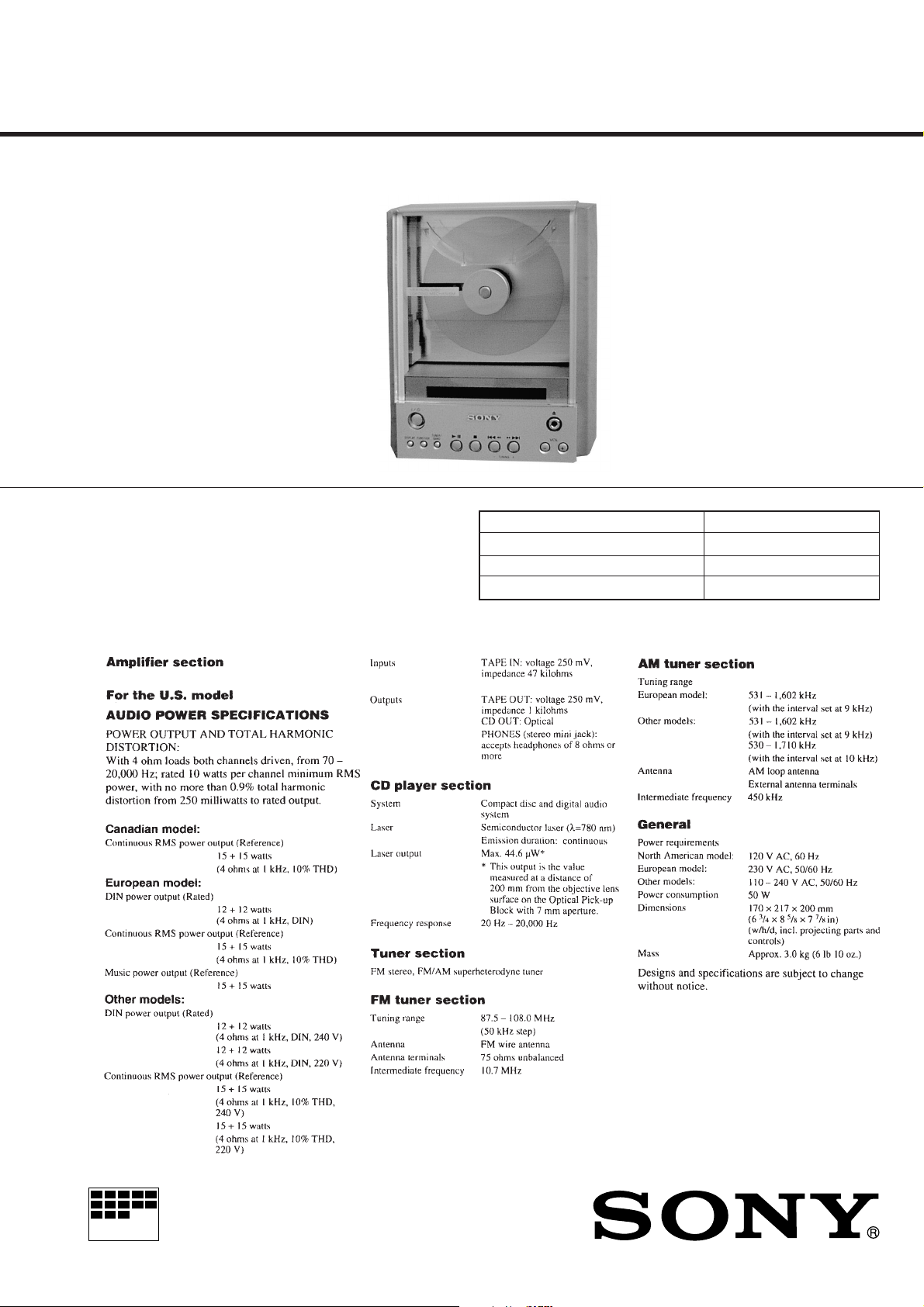
HCD-EX1
SERVICE MANUAL
HCD-EX1 is the amplifier, CD and
tuner section in CMT-EX1.
Model Name Using Similar Mechanism NEW
Mechanism Type CDM-60
Base Unit Type KSM-770ACA/S-NP
Optical Pick-up Type KSS-770A/S-N1
SPECIFICATIONS
US Model
Canadian Model
AEP Model
UK Model
E Model
Australian Model
Tourist Model
MICROFILM
COMPACT COMPONENT SYSTEM
1
Page 2

Laser component in this product is capable of emitting radiation
exceeding the limit for Class 1.
This appliance is classified as
a CLASS 1 LASER product.
The CLASS 1 LASER PRODUCT MARKING is located on
the rear exterior.
This caution
label is located
inside the unit.
CAUTION
Use of controls or adjustments or performance of procedures
other than those specified herein may result in hazardous radiation exposure.
SAFETY CHECK-OUT
After correcting the original service problem, perform the following safety checks before releasing the set to the customer:
Check the antenna terminals, metal trim, “metallized” knobs, screws,
and all other exposed metal parts for AC leakage. Check leakage as
described below.
LEAKAGE
The AC leakage from any exposed metal part to earth Ground and
from all exposed metal parts to any exposed metal part having a
return to chassis, must not exceed 0.5 mA (500 microampers). Leakage current can be measured by any one of three methods.
1. A commercial leakage tester, such as the Simpson 229 or RCA
WT-540A. Follow the manufacturers’ instructions to use these
instruments.
2. A battery-operated AC milliammeter. The Data Precision 245
digital multimeter is suitable for this job.
3. Measuring the voltage drop across a resistor by means of a VOM
or battery-operated AC voltmeter. The “limit” indication is 0.75
V, so analog meters must have an accurate low-voltage scale.
The Simpson 250 and Sanwa SH-63Trd are examples of a passive VOM that is suitable. Nearly all battery operated digital
multimeters that have a 2V AC range are suitable. (See Fig. A)
To Exposed Metal
Parts on Set
Notes on chip component replacement
• Never reuse a disconnected chip component.
• Notice that the minus side of a tantalum capacitor may be
damaged by heat.
Flexible Circuit Board Repairing
• Keep the temperature of soldering iron around 270˚C
during repairing.
• Do not touch the soldering iron on the same conductor of the
circuit board (within 3 times).
• Be careful not to apply force on the conductor when soldering
or unsoldering.
0.15µF
Ω
1.5k
Earth Ground
AC
voltmeter
(0.75V)
Fig. A. Using an AC voltmeter to check AC leakage.
SAFETY-RELATED COMPONENT WARNING !!
COMPONENTS IDENTIFIED BY MARK ! OR DO TTED LINE
WITH MARK ! ON THE SCHEMATIC DIAGRAMS AND IN
THE PARTS LIST ARE CRITICAL TO SAFE OPERATION.
REPLACE THESE COMPONENTS WITH SONY PARTS
WHOSE PART NUMBERS APPEAR AS SHOWN IN THIS
MANUAL OR IN SUPPLEMENTS PUBLISHED BY SONY.
2
ATTENTION AU COMPOSANT AYANT RAPPORT
À LA SÉCURITÉ!!
LES COMPOSANTS IDENTIFIÉS P AR UNE MARQUE ! SUR
LES DIAGRAMMES SCHÉMATIQUES ET LA LISTE DES
PIÈCES SONT CRITIQUES POUR LA SÉCURITÉ DE
FONCTIONNEMENT. NE REMPLA CER CES COMPOSANTS
QUE PAR DES PIÈCES SONY DONT LES NUMÉROS
SONT DONNÉS DANS CE MANUEL OU DANS LES
SUPPLÉMENTS PUBLIÉS PAR SONY.
Page 3

TABLE OF CONTENTS
1. SERVICING NOTE .......................................................... 4
2. GENERAL ..........................................................................7
3. DISASSEMBLY
3-1. Back Cover and Case ............................................................ 9
3-2. Panel Board and Stabilizer....................................................9
3-3. AMP Block ......................................................................... 10
3-4. CD Block ............................................................................ 10
3-5. Motor ASSY and CAM....................................................... 11
3-6. Base Unit.............................................................................11
3-7. Main Board and Power Board ............................................ 12
4. ELECTRICAL ADJUSTMENT ..............................13
5. DIAGRAMS
5-1. Circuit Boards Location ...................................................... 14
5-2. Printed Wiring Board – Main Section –.............................. 16
5-3. Schematic Diagram – Main (1/3) Section –........................ 18
5-4. Schematic Diagram – Main (2/3) Section –........................ 19
5-5. Schematic Diagram – Main (3/3) Section – ........................ 20
5-6. Printed Wiring Board – LED/Loading/SW Section –.........21
5-7. Schematic Diagram
– LED/Loading/SW Section Section – ............................... 21
5-8. Printed Wiring Board – AMP Section –..............................22
5-9. Schematic Diagram – AMP Section –.................................23
5-10. Printed Wiring Board – Panel Section –........................... 24
5-11. Schematic Diagram – Panel Section – ............................. 25
5-12. Printed Wiring Board – Power Section – ......................... 26
5-13. Printed Wiring Board – Power Section – ......................... 27
5-14. Printed Wiring Board – REG Section –............................ 28
5-15. Schematic Diagram – REG Section – .............................. 29
5-16. IC Block Diagrams ........................................................... 30
5-17. IC Pin Functions ............................................................... 32
NOTES ON HANDLING THE OPTICAL PICK-UP BLOCK
OR BASE UNIT
The laser diode in the optical pick-up block may suffer electrostatic
break-down because of the potential difference generated by the
charged electrostatic load, etc. on clothing and the human body.
During repair, pay attention to electrostatic break-down and also
use the procedure in the printed matter which is included in the
repair parts.
The flexible board is easily damaged and should be handled with
care.
NOTES ON LASER DIODE EMISSION CHECK
The laser beam on this model is concentrated so as to be focused on
the disc reflective surface by the objective lens in the optical pickup block. Therefore, when checking the laser diode emission, observe from more than 30 cm away from the objective lens.
LASER DIODE AND FOCUS SEARCH OPERATION
CHECK
Carry out the “S curve check” in “CD section adjustment” and check
that the S curve waveform is output four times.
6. EXPLODED VIEWS
6-1. Front and Case Section ....................................................... 36
6-2. Chassis Section ................................................................... 37
6-3. Mechanism Section ............................................................. 38
6-4. Base Unit Section................................................................ 39
7. ELECTRICAL PARTS LIST .................................40
3
Page 4
ADJUSTMENT OF CAM PHASE
Cam
Boss
SECTION 1
SERVICING NOTE
Absorber Absorber
Cam
SW lever
Insert the cam so that the boss touches the SW lever
at the left shown in the figure.
With the phase adjusted, attach the parts using the following procedure.
STEP1
Insert the boss of the slider (3) in the groove of
the cam.
Boss
Slider (3)
Cam
STEP3
Insert the boss of the lever (1) in the hole of the
slider (3) and attach.
Lever (1)
SW lever
Rotate the cam in the arrow direction, and adjust the
phase until the boss touches the SW lever shown in
the figure.
Boss
Boss
Lever (1)
Boss
Screw
(PTTWH2.6x8)
Mecha cover
4
STEP2
Set the mecha cover to the groove
on the slider (3) and attach.
Screw
(BVTP2.6x8)
Groove of slider (3)
Screw
(BVTP2.6x8)
Hole of slider (3)
STEP4
While bending the slider (2) slightly in the arrow
direction, insert it in the groove of the guides (L)
and (R) and attach.
Boss (Four point)
Slider (2)
Guide (L)
Guide (R)
Page 5
Shipment Mode
• Mode for setting the state of the unit to the state at shipment. When returning the unit to the customer after completing servicing, set to the
shipment mode.
Procedure :
Connect the power plug to the outlet while pressing the 1/u button.
Change-over of AM tuner Step between 9kHz and 10kHz.
• A step of AM channels can be changed over between 9kHz and 10kHz.
Procedure:
1. Press 1/u button to turn on the set ON.
2. Select the function “TUNER”, and press the TUNER/BAND button to select the BAND “AM”.
3. Press the 1/u button to turn on the set OFF.
4. Press 1/u button while pressing the )+/TUNING + button, and the display of liquid crystal indicator tube changes to “AM 9k
STEP” or “AM 10k STEP”, and thus the channel step is changed over.
Switching the TAPE IN input level attenuate function ON/OFF
• The attenuate function of the line input level (TAPE IN) of this unit can be turned ON/OFF.
Procedure:
1. Press the 1/u button to turn ON the power.
2. Press the FUNCTION button and set the function to “TAPE”.
3. Press the 1/u button to turn OFF the power.
4. While pressing the p button, press the 1/u button to turn ON the power.
5. After “POWER ON” is displayed, “ATT ON” and “ATT OFF” are displayed, and the attenuate function can be switched ON/OFF.
LCD All Lit and Key Check Mode
Procedure:
1. While pressing the FUNCTION button and ^ button, connect the power plug to the outlet.
2. When the test mode is set, the characters “STEP” are displayed on the LCD.
3. While pressing the DISPLAY button, press the ^ button. The whole LCD lights up.
4. Each time the FUNCTION button is pressed, the display switches between all lit n partial lighting 1 n partial lighting 2 n all lit.
5. When the p button is pressed, “KEY 0” is displayed and the key check mode is set.
6. Each time the button is pressed, the counter counts up. Buttons once pressed will not be counted when pressed again.
When all buttons have been pressed, “KEY OK” is displayed.
7. To end, press the 1/u button to turn OFF the power, and disconnect the power plug from the outlet.
Note:
Pressing buttons other than those specified in steps 4 and 5 displays modes not used in servicing. In such cases, press the 1/u button to exit
the mode, and repeat from step 3 again.
All lit
Partial lighting 1
Partial lighting 2
5
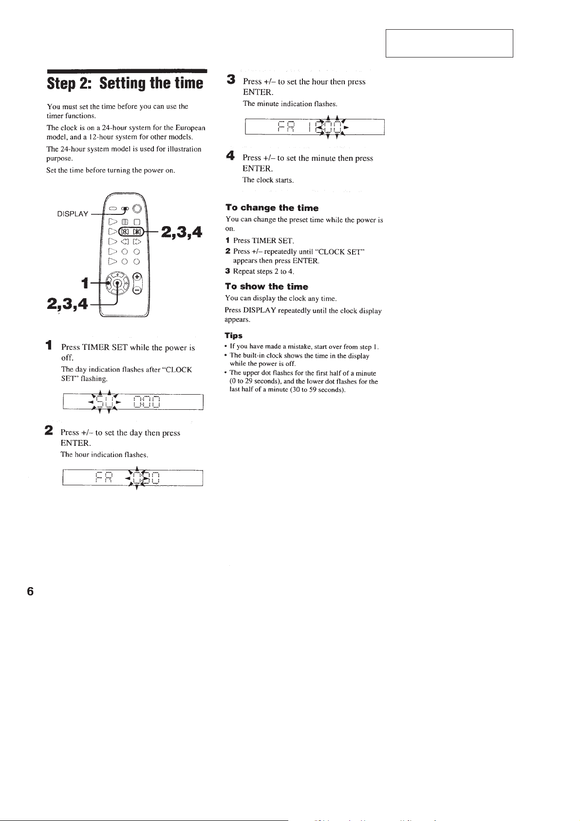
Page 6
Displaying the CD Text
• This unit is equipped with a simple CD text display function.
The text is displayed only for the first 20 songs. As it will not be displayed from the 21st song, do not suspect a fault.
In some cases, special characters may not be displayed or may be substituted by other characters. This is not a fault.
Aging Mode
• The aging mode automatically repeats the operations of the CD.
When an error occurs:
Aging stops
When no error occurs:
Aging is performed repeatedly.
Procedure:
1. Set any CD. (One with a short playback time of the final track is recommended.)
2. While pressing the FUNCTION button and ^ button, connect the power plug to the outlet.
3. When the test mode is set, the characters “STEP” is displayed on the LCD.
4. When the ^ button is pressed while pressing the DISPLAY button, “AGING” will be displayed, and aging is performed in the
following sequence. While aging is performed, “REP” will be displayed blinking.
5. Pressing the DISPLAY button during aging displays the cycle number (@ CY where @ is the number of agings).
6. To end aging, press the 1/u button, turn OFF the power, and disconnect the power plug from the outlet.
Sequence during aging
Reads the TOC
Pauses
Accesses first track
Accesses last track
Plays last track
Eject disc (“OPEN” displayed)
Load disc (“CLOSE” displayed)
Displays number of cycles
Power OFF
Power ON
6
Page 7
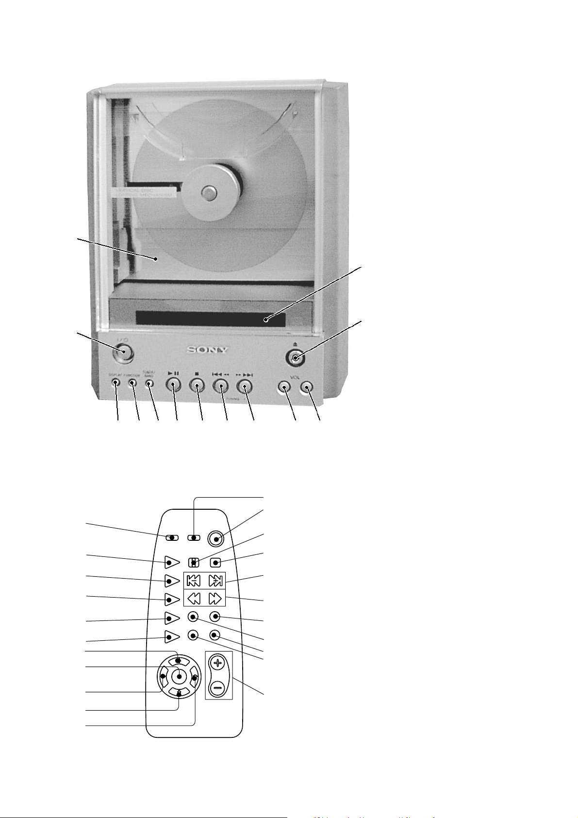
SECTION 2
GENERAL
Front Panel
2
1
LOCATION OF PARTS AND CONTROLS
1 1/u (power) button
2 DISC tray
3 Display window
4 6 button
5 VOLUME + button
6 VOLUME – button
7 )+/TUNING + button
8 =0/TUNING – button
9 p (stop) button
10 ^ button
11 TUNER/BAND button
12 FUNCTION button
13 DISPLAY button
3
4
Remote
1
2
3
4
5
6
7
8
9
10
11
1112
913 8 56
10
7
12
13
14
15
16
17
18
19
20
21
22
1 OPEN/CLOSE button
2 CD · button
3 TUNER/BAND button
4 FUNCTION button
5 CD PLAY MODE button
6 TUNING MODE button
7 MEMORY button
8 ENTER button
9 TIMER SET button
10 SLEEP button
11 TIMER SELECT button
12 DISPLAY button
13 1/u (power) button
14 ∏ button
15 π button
16 ≠/± (AMS) TUNING +/– button
17 º/‚ button
18 REPEAT button
19 DSG button
20 SURROUND button
21 STEREO/MONO button
22 VOLUME +/– button
• AMS is the abbreviation for Automatic Music Sensor.
7
Page 8
This section is extracted from
instruction manual.
8
Page 9

SECTION 3
DISASSEMBLY
Note: Follow the disassembly procedure in the numerical order given.
3-1. BACK COVER AND CASE
Case
5
4
Two screws (KTP3x8)
Two screws (BVTT3x5)
6
Top panel
7
Side ornamental
9
3
Two screws (KTP3x8)
2
Rear cover
Screw (KTP3x8)
8
3-2. PANEL BOARD AND STABILIZER
6
Remove the stabilizer
in the direction arrow.
Stabilizer
Stabiholder
Five screws (BVTP2.6x8)
Side ornamental
!¡
0
Screw (KTP3x8)
1
Two claws
3
Two screws (BVTT3x5)
2
Claw
4
Front panel assy
5
Flat type wire
(7 core)
7
PANEL board
1
Remove the Earth clip
9
Page 10

3-3. AMP BLOCK
Connector
1
AMP board: CN801
Connector
2
AMP board: CN810
Screw (BVTT3x5)
4
AMP block
7
Connector
3
AMP board: CN802
Screw (BVTT3x5)
5
Screw (BVTT3x5)
6
3-4. CD BLOCK
6
Connector
MAIN board: CN351
5
Flat type wire (16 core)
4
Connector
MAIN board: CN301
3
Screw (BVTT3x5)
CD block
7
2
Screw (BVTT3x5)
1
Two screws (BVTT3x5)
10
Page 11
3-5. MOTOR ASSY AND CAM
(
)
)
Note: Adjustment of the phase is required in assembly.Refer to
"Section 1. Servicing Note" for details.
4
Two screws (2.4x6)
Diskholder
6
Slider (2)
8
5
Two screws (2.4x6)
Slider (3)
!£
!¢
Cam
!∞
Screws (BTP2.6x8)
Two screws (BVTP2.6x8)
0
Lever (1)
9
Two screws (BVTP2.6x8)
!¡
Mecha cover
!™
7
Screws (PTPWH2.6x?)
3-6. BASE UNIT
8
Coil spring
1
9
Two screws
(PTPWH2.6)
SW cam
!§
1
Two screws (BVTP2.6x8)
Two screws (BVTP2.6x8)
Guide (L)
2
5
0
Coil spring
Two screws (PTPWH2.6)
!¡
Slider (4)
7
2
Two screws
Slider (1)
3
Motor assy
BVTP2.6x8
Slider (4)
6
3
Two screws
(BVTP2.6x8
Guide (R)
4
!™
BU holder
!£
Screws (PTPWH2.6)
!¢
Two screws (PTPWH2.6)
Pick up assy
!∞
11
Page 12
3-7. MAIN BOARD AND POWER BOARD
)
Main board
4
Flat type wire (7 core)
6
Spacer
5
7
8
Two screws
(BVTT3x5)
Screw (PTPWH2.6)
3
Flat type wire
(13 core)
9
Two screws
(BVTT3x5)
Back panel
!¶
1
Screw (BVTT3x5)
!¢
Two screws
(BVTP3x8)
2
Two screws
(BVTP3x8)
!¡
Screw (BVTT3x5
!§
Three screws
(BVTT3x5)
Power cord
@º
Screw (BVTT3x5)
!•
Power board
@¡
0
Screw (BVTT3x5)
Two screws
!ª
(BVTT3x5)
Sealed case
!™
REG board
!∞
Connector
!£
POWER board: CN903
12
Page 13
SECTION 4
TP
(VC)
TP
(FEI)
TP
(RF)
TP
(FE)
TP
(TE)
IC303
IC301
ELECTRICAL ADJUSTMENT
Note:
1. CD Block is basically constructed to operate without adjustment.
Therefore, check each item in order given.
2. Use YEDS-18 disc (3-702-101-01) unless otherwise indicated.
3. Use an oscilloscope with more than 10MΩ impedance.
4. Clean the object lens by an applicator with neutral detergent when
the signal level is low than specified value with the following
checks.
S Curve Check
oscilloscope
MAIN board
TP (FE)
TP (VC)
+
–
Procedure :
1. Connect the oscilloscope to test points TP (FE) and TP (VC).
2. Connect TP (FEI) and TP (VC) of the MAIN board with lead
wires.
3. Press the 1/u button to turn the set ON.
4. Press the ^ button, load and eject the disc (YEDS-18) to
perform focus search.
5. Check the symmetry and peak to peak level of the oscilloscope
waveform (S curve) at this time.
S-curve waveform
symmetry
Note: Clear RF signal waveform means that the shape “◊” can be
clearly distinguished at the center of the waveform.
RF signal waveform
VOLT/DIV : 200mV
TIME/DIV : 500ns
level : 1.2 ± 0.2 Vp-p
Checking Location : MAIN board
E-F Balance (1 Track Jump) check
oscilloscope
MAIN board
TP (TE)
TP (VC)
+
–
Procedure:
1. Connect oscilloscope to test point TP (TE) and TP (VC) on MAIN
board.
2. Press the 1/u button to turn the unit ON.
3. Put disc (YEDS-18) in to play the number five track.
4. Press the ^ button, to pause.
5. Check the level (B) of the oscilloscope's waveform and the DC
voltage (A) of the center of the Traverse waveform.
Confirm the following:
A
Within 3.8
B
±
1 Vp-p
6. After check, remove the lead wire connected in step 2.
Note: • T ry to measure several times to make sure than the ratio of
A : B or B : A is more than 10 : 7.
• Take sweep time as long as possible and light up the brightness to obtain best waveform.
Checking Location : MAIN board
RF Level Check
oscilloscope
MAIN board
TP (RF)
TP (VC)
+
–
Procedure :
1. Connect oscilloscope to test point TP (RF) and TP (VC) on MAIN
board.
2. Press the 1/u button to turn the set ON.
3. Put disc (YEDS-18) in and playback 5track.
4. Confirm that oscilloscope waveform is clear and check RF signal level is correct or not.
• A/B x 100 = less then ± 22 (%)
• B = 1.3 ± Vp-p
1 track jump waveform
0V
+0.6
–0.7
level : 1.3
+0.6
±
Vp-p
–0.7
Checking Location : MAIN board
[ MAIN BOARD ] — SIDE A —
Center of the waveform
B
A (DC voitage)
Symmetry
13
Page 14
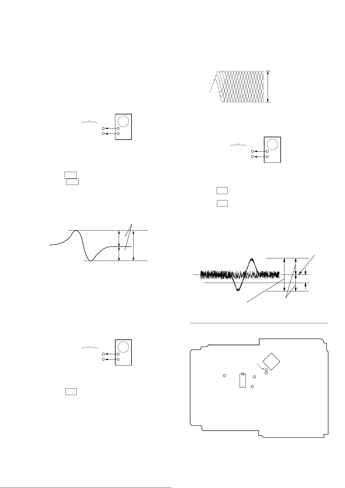
5-1. CIRCUIT BOARDS LOCATION
LED BOARD
SECTION 5
DIAGRAMS
MAIN BOARD
AMP BOARD
PANEL BOARD
REG BOARD
SW BOARD
POWER BOARD
LOADING BOARD
14
Page 15

HCD-EX1
2.5V
APPROX 500mVp-p (PLAY)
2.5V
APPROX 200m Vp-p (PLAY)
THIS NOTE IS COMMON FOR PRINTED WIRING
BOARDS AND SCHEMATIC DIAGRAMS.
(In addition to this, the necessary note is printed
in each block.)
For schematic diagrams.
Note:
• All capacitors are in µF unless otherwise noted. pF: µµF
50 WV or less are not indicated except for electrolytics
and tantalums.
• All resistors are in Ω and 1/
specified.
¢
•
: internal component.
4
W or less unless otherwise
• 2 : nonflammable resistor.
• 5 : fusible resistor.
• C : panel designation.
Note:
The components identified by mark ! or dotted
line with mark ! are critical for safety.
Replace only with part
number specified.
Note:
Les composants identifiés par
une marque ! sont critiques
pour la sécurité.
Ne les remplacer que par une
piéce portant le numéro
spécifié.
• U : B+ Line.
• V : B– Line.
• H : adjustment for repair.
• Voltages and waveforms are dc with respect to ground
under no-signal (detuned) conditions.
• Voltages and waveforms are dc with respect to ground in
service mode.
• Waveforms are taken with a oscilloscope.
Voltage variations may be noted due to normal production tolerances.
no mark : STOP
• Circled numbers refer to waveforms.
• Signal path.
J : CD
c : digital out
• Abbreviation
CND : Canadian model.
For printed wiring boards.
Note:
• X : parts extracted from the component side.
®
•
: Through hole.
• b : Pattern from the side which enables seeing.
(The other layers' patterns are not indicated.)
• Indication of transistor
C
Q
C
EB
These are omitted
These are omitted
EB
WAVEFORMS
– MAIN (1/3) SECTION –
1
3.1Vp-p
16.9MHz
IC304 6 XTO
2
1.2Vp-p
(PLAY)
IC303 %º RF AC
3
IC303 $¡ TE
4
IC303 #ª FE
5
2.4Vp-p
7.5µsec
IC303 @∞ MDP
– MAIN (3/3) SECTION –
6
5Vp-p
32.768kHz
IC701 !£ XT2
7
5.5Vp-p
5MHz
IC701 0 X2
15 15
Page 16

HCD-EX1
• Semiconductor
Location
Ref. No. Location
D139 E-4
D701 D-3
D751 D-3
D752 D-3
D753 D-3
D754 D-4
IC11 1 C-5
IC301 C-3
IC302 B-3
IC303 B-4
IC304 A-5
IC391 B-6
IC451 A-1
IC501 A-6
IC701 D-1
IC751 C-4
5-2. PRINTED WIRING BOARD – MAIN SECTION –
• See page 14 for Circuit Boards Location.
Q113 D-4
Q131 D-4
Q163 D-4
Q301 C-2
Q401 D-6
Q751 D-4
Q771 D-1
Q772 D-1
Q781 C-4
Q782 C-3
(Page 24) (Page 28) (Page 16) (Page 22)
16 16
Page 17

HCD-EX1
17 17
Page 18

HCD-EX1
5-3. SCHEMATIC DIAGRAM – MAIN (1/3) SECTION –
• See page 15 for Waveforms.
• See page 16 for Printed Wiring Board.
• See page 30 for IC Block Diagrams.
• See page 32 for IC Pin Functions.
(Page 21)
(Page 19) (Page 20)
18 18
Page 19

5-4. SCHEMATIC DIAGRAM – MAIN (2/3) SECTION –
• See page 16 for Printed Wiring Board.
HCD-EX1
(Page 18)
(Page 20)
MICON
INTERFACE
(Page 20)
(Page 20)
(Page 20)
(Page 20)
19 19
(Page 25)
Page 20

HCD-EX1
5-5. SCHEMATIC DIAGRAM – MAIN (3/3) SECTION –
• See page 15 for Waveforms.
• See page 16 for Printed Wiring Board.
• See page 34 for IC Pin Functions.
(Page 19)
(Page 19) (Page 19)
(Page 19) (Page 19)
(Page 18)
20 20
(Page 29)
(Page 23)
Page 21

HCD-EX1
5-6. SCHEMATIC DIAGRAM – LED/LOADING/SW SECTION –
• See page 31 for IC Block Diagrams.
5-7. PRINTED WIRING BOARD – LED/LOADING/SW SECTION –
• See page 14 for Circuit Boards Location.
(Page 18)
(Page 28)
21 21
Page 22

HCD-EX1
5-8. PRINTED WIRING BOARD – AMP SECTION –
• See page 14 for Circuit Boards Location.
(Page 28)
22 22
(Page 28)(Page 16)
Page 23

5-9. SCHEMATIC DIAGRAM – AMP SECTION –
(Page 20)
HCD-EX1
(Page 29)
(Page 29)
23 23
Page 24

HCD-EX1
5-10. PRINTED WIRING BOARD – PANEL SECTION –
• See page 14 for Circuit Boards Location.
(Page 16)
24 24
Page 25

5-11. SCHEMATIC DIAGRAM – PANEL SECTION –
HCD-EX1
(Page 19)
25 25
Page 26

HCD-EX1
5-12. PRINTED WIRING BOARD – POWER SECTION –
• See page 14 for Circuit Boards Location.
• Semiconductor
Location
Ref. No. Location
D2 C-3
D3 C-3
D4 B-3
D6 B-3
D7 C-4
D10 E-3
D11 E-3
D12 D-3
D13 D-3
D21 D-2
D22 C-2
D901 B-2
D911 B-2
D931 A-3
D941 A-2
IC1 C-4
IC933 A-1
IC951 B-1
Q21 D-2
Q22 D-2
Q23 D-2
Q951 D-1
(Page 28)
26 26
Page 27

5-13. SCHEMATIC DIAGRAM – POWER SECTION –
HCD-EX1
(Page 29)
27 27
Page 28

HCD-EX1
(Page 22)
5-14. PRINTED WIRING BOARD – REG SECTION –
• See page 14 for Circuit Boards Location.
(Page 22)
(Page 26)
(Page 16)
28 28
Page 29

5-15. SCHEMATIC DIAGRAM – REG SECTION –
HCD-EX1
(Page 23)
(Page 27)
(Page 20)
29 29
Page 30

HCD-EX1
5-16. IC BLOCK DIAGRAMS
• MAIN Board (1/3)
IC301 CXA2568M-T6
APC PD AMP
VEE
1
HOLD
AGCVTH
LD
PD
VEE
VC
LRCIN
DIN
BCKIN
CLKO
XTI
XTO
DGND
VEE
2
3
4
A
5
B
6
C
7
D
8
9
F
10
E
11
12
VREF
VEE
VC
VC
VC BUFFER
VC
IC304 PCM1710U-B/1K
1
2
3
4
5
6
7
INPUT
INTERFACE DIGITAL
TIMING
CONTROL
VC
RF SUMMING AMP RF_EQ_AMP
VC
VC
VC
VCC
VEE
VCC
VEE
VC
FILTER
NOISE
SHAPER
APC LD AMP
VC
ERROR AMP
FOCUS
TRACKING
ERROR AMP
VC
VCC
IC303 CXD2585Q
XTSL
SQCK
76
SQSO
SERVO
Interface
XOLT
7475 73
SOCK
SOUT
D/A
Interface
Sub Code
Processor
Sequencer
Servo
Auto
MIRR
DFCT
FOK
Error
Corrector
EXCK
SCSY
SBSO
80
79 77
78
VCC
24
VCC
23
LC/PD
LD_ON
22
HOLD_SW
21
AGCCONT
20
(50%/30%
OFF)
RF_BOT
19
VC
RFTC
18
RF_1
17
RFO
16
RFE
15
FE
14
TE
13
28
ML/DSD
MC/DM2
MODE
CONTROL
27
26
25
24
23
22
MD/DM1
MUTE
MODE
CKSL
DGND
DVDD0
XRST
MUTE
DATA
XLAT
CLOCK
SENS
SCLK
ATSK
WFCK
XUGF
XPCK
GFS
V2PO
SCOR
C4M
WDCK
DVSS0
COUT
MIRR
1
2
3
4
5
6
7
8
9
10
11
12
13
14
15
16
17
18
19
20
CPU
Interface
XTAO
72
Digital
XTAI
71
Clock
Generator
EFM
demodurator
CLV
70
DVSS2
69
32K
RAM
PWM GENERATOR
FORCUS PWM
GENERATOR
TRACKING PWM
GENERATOR
SLED PWM
GENERATOR
LRCK
BCK
EMPH
PCMD
67
68
66 65
SIGNAL PROCESSOR BLOCK
A/D
Converter
Digital
PLL
Asymmetry
Corrector
SERVO BLOCK
SERVO DSP
FOCUS SERVO
TRACKING
SLED SERVO
OPAmp
Analog SW
64
Digital
SERVO
DOUT
OUT
63
MD2
ASYE
62 61
DVDD2
60
59
58
57
56
55
54
53
52
51
50
49
48
47
46
45
44
43
42
41
VPCO
V16M
VCTL
BIAS
AVDD1
PCO
FILI
FILO
CLTV
AVSS1
RFAC
ASYI
ASYO
AVDD0
IGEN
AVSSO
ADIO
RFDC
CE
TE
V
VCC2R
GND2R
EXT1R
EXT2R
VOUTR
GND1
8
DD
9
10
11
12
13
14
5-LEVEL DAC
RIGHT
LOW-PASS FILTER
RIGHT
3-STAGE AMP
RIGHT
5-LEVEL DAC
LEFT
LOW-PASS FILTER
LEFT
3-STAGE AMP
LEFT
21
DD
V
20
VCC2L
19
GND2L
18
EXT1L
EXT2L
17
16
VOUTL
V
CC1
15
21
22
FOK
DFCT
2423
PWMI
25 26
LOCK
MDP
27
SSTP
28
FETO
29
SFDR
DVDD1
30
31
11
SRDR
32
11
TFDR
33 34
TRDR
FFDR
FRDR
35 36 37
TEST
DVSS1
TES1
38 39 40
FE
VC
SE
30 30
Page 31

• LOADING Board
IC351 LB1641
T.S.D O.C.P
MOTOR
DRIVE
FWD/REV/STOP
CONTROL LOGIC
MOTOR
DRIVE
2 3
1
GND
DRIVE
MOTOR
NOISE
FILTER
5 6 7 8 9 10
4
VCC 1
FWD.IN
REV.IN
CLAMP
VCC 2
NOISE
FILTER
DRIVE
MOTOR
31
Page 32

5-17. IC PIN FUNCTIONS
• IC303 DIGITAL SERVO & DIGITAL SIGNAL PROCESSOR (CXA2585Q) (MAIN Board (1/3))
Pin No.
1
2
3
4
5
6
7
8
9
10
11
12
13
14
15
16
17
18
19
20
21
22
23
24
25
26
27
28
29
30
31
32
33
34
35
36
37
38
39
40
Pin Name I/O Function
–
DVDD
XRST
MUTE
DATA
XLAT
CLOK
SENS
SCLK
ATSK
WFCK
XUGF
XPCK
GFS
C2PO
SCOR
CM4
WDCK
DVSS
COUT
MIRR
DFCT
FOK
PWMI
LOCK
MDP
SSTP
FSTO
DVDD1
SFDR
SRDR
TFDR
TRDR
FFDR
FRDR
DVSS1
TEST
TES1
VC
FE
SE
Digital power supply
I
System reset “L” : reset
I
Muting input “H” : mute
I
Serial data input, supplied from CPU
I
Latch input, supplied from CPU
I
Serial data transfer clock input, supplied from CPU
O
SENS signal output to CPU
I
SENS serial data read-out clock input
I/O
Input pin for anti-shock (Connected to ground)
O
WFCK output (Not used)
O
Not used
O
Not used
O
Not used
O
Not used
O
Sub-code sync output
O
4.2336 MHz output (Not used)
O
Word clock output (ƒ = 2Fs)
–
Digital ground
I/O
Numbers of track counted signal input/output (Not used)
I/O
Mirror signal input/output
I/O
Defect signal input/output
I/O
Focus OK input/output
I
Spindle motor external control input (Connected to ground)
I/O
GFS is sampled by 460 Hz. H when GFS is H (Not used)
O
Output to control spindle motor servo
I
Input signal to detect disc inner most track
O
2/3 divider output of pin 71
–
Digital power supply
O
Sled drive output
O
Sled drive output
O
Tracking drive output
O
Tracking drive output
O
Focus drive output
O
Focus drive output
–
Digital ground
I
TEST pin connected normally to ground
I
TEST pin connected normally to ground
I
Center voltage input pin
I
Focus error signal input
I
Sled error signal input
• Abbreviation
GFS : Guarded Frame Sync
32
Page 33

Pin No. Pin Name
41
42
43
44
45
46
47
48
49
50
51
52
53
54
55
56
57
58
59
60
61
62
63
64
65
66
67
68
69
70
71
72
73
74
75
76
77
78
79
80
TE
CE
RFDC
ADIO
AVSS0
IGEN
AVDD0
ASYO
ASYI
RFAC
AVSS1
CLTV
FILO
FILI
PCO
AVDD1
BIAS
VCTL
V16M
VPCO
DVDD2
ASYE
MD2
DOUT
LRCK
PCMD
BCLK
EMPH
XTSL
DVSS2
XTAI
XTAO
SOUT
SOCK
XOLT
SQSO
SQCK
SCSY
SBSO
EXCK
I/O Function
Tracking error signal input
I
Center servo analog input
I
RF signal input
I
Test pin (Not used)
O
Analog ground
–
Stabilized current input for operational amplifiers
I
Analog power supply
–
EFM full swing output
O
Asymmetry comparate voltage input
I
EFM signal input
I
Analog ground
–
Control voltage input for master VCO1
I
Filter output for master PLL
O
Filter input for master PLL
I
Charge-pump output for master PLL
O
Analog power supply
–
Asymmetry circuit constant current input
I
VCO2 control voltage input for wide band EFM PLL (Connected to VDD)
I
VCO2 oscillator input/output for wide band EFM PLL (Not used)
I/O
Charge-pump output for wide band EFM PLL (Not used)
O
Digital power supply
–
Asymmetry circuit ON/OFF input “L” OFF, “H” : ON (Connected to VDD)
I
Digital-out ON/OFF control input (Connected to VDD)
I
Digital-out output pin
O
D/A interface LR clock output (ƒ = Fs)
O
D/A interface serial data output
O
D/A interface bit clock output
O
Playback disc output in emphasis mode (Not used)
O
X'tal selection input (Connected to ground)
I
Digital ground
–
X'tal oscillator circuit input
I
X'tal oscillator circuit output (Not used)
O
Serial data output in servo block (Not used)
O
Serial data read clock output in servo block (Not used)
O
Serial data latch output in servo block (Not used)
O
Sub-Q 80-bit and PCM peak level data output (CD text data output)
O
Clock input for SQSO read-out
I
Connected to ground
I
Sub-P through Sub-W serial output (Not used)
O
Clock input for SBSO read-out (Connected to ground)
I
• Abbreviation
EFM : Eight to Fourteen Modulation
PLL : Phase Locked Loop
33
Page 34

• IC701 uCOM (UPD780306GF-024-3BA) (MAIN Board (3/3))
Pin No. Pin Name I/O
1 TUNED I ST tuning
2 PLL_CE O ST PLL CE
3 PLL_DATAI I ST PLL IN data
4 PLL_DAT AO O ST PLL OUT data
5 PLL_CLK O ST PLL CLK
6 GND – Ground (Programing)
7 XOUT –
8 XIN –
9 VDD1 – Ground
10 XT1 –
11 XT2 –
12 RESET I uCOM reset in
13 REMOTE I SIRCS IN
14 RDS_CLK I ST RDS clock
15 POWDET I AC power down detect
16 SCOR I CD SCOR
17 RDS_DATA I ST RDS data
18 SENSE I CD SENS
19 SUB Q I CD SUBQ IN data
20 BACKLIGHT O LCD back light
21 SERVO_CK O CD SQCK/SCLK (for serial in)
22 XLAT O CD data latch
23 XRST O CD (BC) reset
24 SCLK O CD CLOCK/PCM1710 CLK
25 MUTE_D O CD digital mute
26 CD_POWER O CD (BD) power
27 AVSS – Ground
28 KEYIO_1 I
29 KEYIO_2 I
30 BAND_AREA I Destination setting
31 DA_LAT O PCM1710 latch
32 LPH O CD LPH
33 LDON O CD LASER ON
34 OPEN_SW I OPEN SW
35 CLOSE_SW I CLOSE SW
36 VDD0 –
37 AVREF –
38 AMP_MUTE O POWER AMP MUTE
39 DATA O CD CMD/PCM1710 OUT DATA
40 VSS1 – Ground
41 OPEN O CD loading motor open
42 CLOSE O CD loading motor close
43 POWER O System power
44 TA_MUTE O TA MUTE
45 SP_RELAY O Speaker relay
46 ST_MUTE O ST MUTE
47 SLEEP O Power supply sleep control
48 VOL_CLK O VOL CLK
49 VOL_DATA O VOL OUT data
50 VOL_STB O VOL STB
5MHz (Main clock)
32KHz (Sub clock)
KEY
+5V
Function
34
Page 35

Pin No.
51 to 54 COM0 to COM3 O LCD COMMON
55 BIAS O LCD DRIVE POWER
56 to 58 VLC0 to VLC2 O LCD DRIVER POWER
59 VSS0 O Ground
60 to 99 SEG0 to SEG39 O FL segment signal output
100 STEREO I ST STEREO
Pin Name
I/O
Function
35
Page 36

SECTION 6
EXPLODED VIEWS
NOTE:
• -XX, -X mean standardized parts, so they may have
some difference from the original one.
• Items marked “*” are not stocked since they are
seldom required for routine service. Some delay
should be anticipated when ordering these items.
• Color Indication of Appearance Parts Example:
KNOB, BALANCE (WHITE)
Â
Parts color
6-1. FRONT PANEL AND CASE SECTION
not supplied
not supplied
14
13
10
23
11
• The mechanical parts with no reference number in
the exploded views are not supplied.
• Hardware (# mark) list and accessories and packing materials are given in the last of this parts list.
• Abbreviation
CND : Canadian model
19
18
#1
#2
17
The components identified by
mark ! or dotted line with mark
! are critical for safety.
Replace only with part number
specified.
Les composants identifiés par une
marque ! sont critiques pour la
sécurité.
Ne les remplacer que par une
piéce portant le numéro spécifié.
21
#2
20
12
15
22
#2
#2
5
22
7
6
4
1
Ref. No. Part No. Description Remark
1 4-969-961-11 EMBLEM(NO.4), SONY
2 4-222-620-01 RING (EJECT)
3 4-222-713-01 PANEL(BASE), FRONT
4 4-222-720-01 BUTTON(PLAY)
5 4-222-719-01 BUTTON(POWER)
6 4-222-742-01 SPRING(EJECT)
7 4-222-743-01 SPRING(EARTH)
8 A-4426-743-A PANEL MOUNTED PC BOARD
9 1-769-889-11 WIRE(FLAT TYPE) (7 CORE)
10 X-4952-306-1 WINDOW (GLASS) ASSY (US,CND)
10 X-4952-307-1 WINDOW (GLASS) ASSY (EXCEPT US,CND)
11 4-222-707-01 YOKE(MG)
12 4-222-703-01 MAGNET
#1
2
3
17
not supplied
16
9
22
8
#2
Ref. No. Part No. Description Remark
13 4-222-709-01 YOKE(ST)
14 4-222-704-01 STABILIZER
15 4-222-711-01 PLATE(L), SIDE
16 4-222-710-01 PLATE(R), SIDE
17 4-985-672-01 SCREW(+PTPWHM2.6), FLOATING
18 4-222-712-01 PLATE, TOP
19 4-222-716-01 CASE
20 4-222-718-01 COVER(PIN JACK)
21 4-222-717-01 COVER(BACK)
22 4-951-620-01 SCREW (2.6x8), +BVTP
23 3-927-664-01 SCREW (2x3)
36
Page 37

6-2. CHASSIS SECTION
not supplied
#1
#1
not supplied
53
#3
#3
not supplied
not supplied
not supplied
#1
#1
67
#3
#1
61
not supplied
56
62
63
#3
66
64
#3
not supplied
59
66
55
not supplied
54
#3
not supplied
58
(US/CND)
60
60
#1
#3
#1
#3
#1
#1
#1
57
(E)
#1
#1
52
#1
51
#1
51
Ref. No. Part No. Description Remark
51 4-220-455-01 FOOT(FELT)
52 4-222-715-01 PLATE, BOTTOM
53 A-4426-745-A AMP MOUNTED PC BOARD (US,CND)
53 A-4426-754-A AMP MOUNTED PC BOARD (EXCEPT US,CND)
54 A-4426-744-A POWER MOUNTED PC BOARD (US,CND)
54 A-4426-753-A POWER MOUNTED PC BOARD (EXCEPT US,CND)
* 55 1-675-407-11 REG BOARD
56 4-985-672-01 SCREW(+PTPWHM2.6), FLOATING
57 3-703-244-00 BUSHING (2104), CORD
58 4-222-730-01 PANEL, BACK
59 A-4426-742-A MAIN MOUNTED PC BOARD (US,CND)
(UK)
65
(AEP/UK)
#1
not supplied
The components identified by
mark ! or dotted line with mark
! are critical for safety.
Replace only with part number
specified.
Ref. No. Part No. Description Remark
59 A-4426-752-A MAIN MOUNTED PC BOARD (EXCEPT US,CND)
! 60 1-575-651-21 CORD,POWER (AEP,UK)
! 60 1-783-531-31 CORD,POWER (US,CND)
61 1-674-910-11 LED BOARD
62 1-791-698-11 WIRE (FLAT TYPE) (16 CORE)
63 1-769-973-11 WIRE (FLAT TYPE) (13 CORE)
64 1-693-407-13 TUNER (US,CND)
64 1-693-408-12 TUNER (EXCEPT US,CND)
! 65 1-770-019-11 ADAPTOR, CONVERSION PLUG 3P (UK)
66 3-314-903-01 CUSHION
67 4-222-714-01 HOUSE, LAMP
60
(HK)
60
(AUS)
60
Les composants identifiés par une
marque ! sont critiques pour la
sécurité.
Ne les remplacer que par une
piéce portant le numéro spécifié.
37
Page 38

6-3. MECHANISM SECTION
102
105
124
107
106
105
114
104
105
105
#5
107
113
109
108
104
104 124
116
104
115
110
#4
#5
117
104
111
not supplied
119
113
125
104
120
122
124
112
118
126
121
124
124
123
104
123
124
103
128
127
101
Ref. No. Part No. Description Remark
101 4-222-746-01 PLATE (CD) (LOWER), ORNAMENTAL
102 4-222-745-01 PLATE (CD) (UPPER), ORNAMENTAL
103 4-222-701-01 PANEL, MECHANICAL
104 4-985-672-31 SCREW (+PTPWHM2.6), FLOATING
105 4-222-697-01 RUBBER, FLOATING
106 4-222-692-01 HOLDER, BU
107 4-222-702-01 SPRING, TENSION
108 4-222-685-01 SLIDER (1)
109 4-222-694-01 GEAR(1)
110 4-999-513-01 GEAR, PULLEY
111 4-999-537-01 BELT(LOADING)
112 4-222-695-01 GUIDE (R)
113 4-222-693-01 SLIDER (4)
114 4-222-700-01 GUIDE (L)
115 4-222-687-01 BASE, MECHANICAL
124
Ref. No. Part No. Description Remark
116 4-222-688-01 HOLDER, DISC
117 4-222-813-01 SLIDER (2)
118 4-225-227-01 SPRING (ABSORBER),TENSION COIL
119 4-225-228-01 CAM(A)
120 4-225-226-01 ABSORBER
121 4-222-689-01 SLIDER (3)
122 4-222-690-01 COVER, MECHANICAL
123 4-222-691-01 LEVER (1)
124 4-951-620-01 SCREW (2.6X8), +BVTP
* 125 1-674-908-11 LOADING BOARD
* 126 1-674-909-11 SW BOARD
127 1-791-698-11 WIRE (FLAT TYPE) (16 CORE)
128 3-831-441-99 CUSHION
38
Page 39

6-4. BASE UNIT SECTION
160
159
162
161
155
154
not supplied
156
157
Ref. No. Part No. Description Remark
151 X-2646-555-1 SCREW ASSY, SLED
152 2-647-505-01 SPRING, RACK
! 153 8-820-087-11 OPTICAL PICK-UP KSS-770A/S-N1
154 2-647-506-01 GEAR, MOTOR
155 1-763-381-11 MOTOR, DC
156 2-647-504-01 HOLDER
153
158
151
The components identified by
mark ! or dotted line with mark
! are critical for safety.
Replace only with part number
specified.
Ref. No. Part No. Description Remark
157 2-646-352-01 SCREW, BTP2x8
158 1-960-065-11 HARNESS
159 2-646-358-11 SCREW, BTP1.7x4
160 1-791-698-11 WIRE (FLAT TYPE) (16 CORE)
161 2-647-507-01 TURN TABLE (HIFI)
162 2-627-669-11 SCREW M1.7x2
152
not supplied
Les composants identifiés par une
marque ! sont critiques pour la
sécurité.
Ne les remplacer que par une
piéce portant le numéro spécifié.
39
Page 40

SECTION 7
AMP
Note:
The components identified by
mark ! or dotted line with mark
! are critical for safety.
Replace only with part number
specified.
Les composants identifiés par une
marque ! sont critiques pour la
sécurité.
Ne les remplacer que par une
piéce portant le numéro spécifié.
When indicating parts by reference
number, please include the board
name.
Ref. No. Part No. Description Remark Ref. No. Part No. Description Remark
C801 1-126-047-71 ELECT 4.7uF 20% 50V
C803 1-126-022-11 ELECT 47uF 20% 25V
C804 1-162-219-31 CERAMIC 68PF 5% 50V
C805 1-164-159-21 CERAMIC 0.1uF 50V
C806 1-164-159-21 CERAMIC 0.1uF 50V
C807 1-163-038-91 CERAMIC CHIP 0.1uF 25V
C811 1-126-027-11 ELECT 1000uF 20% 25V
C812 1-126-027-11 ELECT 1000uF 20% 25V
C813 1-164-159-21 CERAMIC 0.1uF 50V
C814 1-164-159-21 CERAMIC 0.1uF 50V
C821 1-126-933-11 ELECT 100uF 20% 16V
C822 1-126-967-11 ELECT 47uF 20% 50V
C851 1-126-047-71 ELECT 4.7uF 20% 50V
C853 1-126-022-11 ELECT 47uF 20% 25V
C854 1-162-219-31 CERAMIC 68PF 5% 50V
C855 1-164-159-21 CERAMIC 0.1uF 50V
C856 1-164-159-21 CERAMIC 0.1uF 50V
LED
A-4426-754-A AMP BOARD, COMPLETE (EXCEPT US,CND)
********************
A-4426-745-A AMP BOARD, COMPLETE (US,CND)
********************
< CAPACITOR >
ELECTRICAL PARTS LIST
• Due to standardization, replacements in the parts list
may be different from the parts specified in the
diagrams or the components used on the set.
• -XX, -X mean standardized parts, so they may have
some difference from the original one.
• Items marked “*” are not stocked since they are
seldom required for routine service. Some delay
should be anticipated when ordering these items.
• RESISTORS
All resistors are in ohms
METAL: Metal-film resistor
METAL OXIDE: Metal Oxide-film resistor
F : nonflammable
• SEMICONDUCTORS
In each case, u: µ , for example:
uA...: µ A..., uPA...: µ PA..., uPB...: µ PB...,
uPC...: µ PC..., uPD...: µ PD...
• CAPACITORS
uF : µ F
• COILS
uH : µ H
• Abbreviation
CND : Canadian model
< RESISTOR >
R801 1-249-417-11 CARBON 1K 5% 1/4W F
R802 1-216-088-00 METAL CHIP 43K 5% 1/10W
R803 1-249-417-11 CARBON 1K 5% 1/4W F
R804 1-249-436-11 CARBON 39K 5% 1/4W
R805 1-249-754-11 CARBON 10 5% 1/2W
(EXCEPT US,CND)
R806 1-249-393-11 CARBON 10 5% 1/4W F
R807 1-216-089-91 RES,CHIP 47K 5% 1/10W
R821 1-216-085-00 METAL CHIP 33K 5% 1/10W
R822 1-216-091-00 METAL CHIP 56K 5% 1/10W
! R823 1-247-739-11 CARBON 100 5% 1/2W F
R851 1-249-417-11 CARBON 1K 5% 1/4W F
R852 1-216-088-00 METAL CHIP 43K 5% 1/10W
R853 1-249-417-11 CARBON 1K 5% 1/4W F
R854 1-249-436-11 CARBON 39K 5% 1/4W
R855 1-249-754-11 CARBON 10 5% 1/2W
(EXCEPT US,CND)
R856 1-249-393-11 CARBON 10 5% 1/4W F
R857 1-216-091-00 METAL CHIP 56K 5% 1/10W
< RELAY >
RY801 1-515-921-11 RELAY (12V)
< CONNECTOR >
* CN801 1-568-943-11 PIN, CONNECTOR 5P
CN802 1-691-766-11 PLUG (MICRO CONNECTOR) 4P
* CN810 1-564-518-11 PLUG, CONNECTOR 3P
< DIODE >
D821 8-719-988-61 DIODE 1SS355TE-17
< IC >
IC801 8-759-333-24 IC LM1876TF
< COIL >
L801 1-420-872-00 COIL, AIR-CORE (EXCEPT US,CND)
L851 1-420-872-00 COIL, AIR-CORE (EXCEPT US,CND)
< TRANSISTOR >
Q821 8-729-900-53 TRANSISTOR DTC114EKA-T146
Q822 8-729-120-28 TRANSISTOR 2SC3052EF-T1-LEF
Q823 8-729-120-28 TRANSISTOR 2SC3052EF-T1-LEF
Q824 8-729-120-28 TRANSISTOR 2SC3052EF-T1-LEF
40
*************************************************************
1-674-910-11 LED BOARD
**********
< CAPACITOR >
C781 1-163-251-11 CERAMIC CHIP 100PF 5% 50V
C782 1-163-251-11 CERAMIC CHIP 100PF 5% 50V
C783 1-163-251-11 CERAMIC CHIP 100PF 5% 50V
< DIODE >
D781 8-719-076-07 DIODE SELU2E10CRW1TP6
D782 8-719-076-07 DIODE SELU2E10CRW1TP6
D783 8-719-076-07 DIODE SELU2E10CRW1TP6
< RESISTOR >
R781 1-216-029-00 METAL CHIP 150 5% 1/10W
R782 1-216-029-00 METAL CHIP 150 5% 1/10W
R783 1-216-029-00 METAL CHIP 150 5% 1/10W
*************************************************************
Page 41

LOADING
Ref. No. Part No. Description Remark Ref. No. Part No. Description Remark
1-674-908-11 LOADING BOARD
**************
< CAPACITOR >
C351 1-104-665-11 ELECT 100uF 20% 16V
C352 1-163-031-11 CERAMIC CHIP 0.01uF 50V
C353 1-163-031-11 CERAMIC CHIP 0.01uF 50V
C354 1-163-031-11 CERAMIC CHIP 0.01uF 50V
< DIODE >
C167 1-126-964-11 ELECT 10uF 20% 50V
C168 1-126-964-11 ELECT 10uF 20% 50V
C169 1-163-006-11 CERAMIC CHIP 560PF 10% 50V
C170 1-136-165-00 MYLAR 0.1uF 5% 50V
C171 1-136-165-00 MYLAR 0.1uF 5% 50V
C176 1-164-344-11 CERAMIC CHIP 0.068uF 10% 25V
C177 1-163-021-91 CERAMIC CHIP 0.01uF 10% 50V
C301 1-163-038-91 CERAMIC CHIP 0.1uF 25V
C302 1-163-038-91 CERAMIC CHIP 0.1uF 25V
C303 1-104-664-11 ELECT 47uF 20% 10V
MAIN
D351 8-719-056-78 DIODE UDZ-TE-17-4.3B
< IC >
IC351 8-759-822-09 IC LB1641
< RESISTOR >
R351 1-216-025-91 RES,CHIP 100 5% 1/10W
**************************************************************
A-4426-742-A MAIN BOARD, COMPLETE (US,CND)
*********************
A-4426-752-A MAIN BOARD, COMPLETE (EXCEPT US,CND)
*********************
< CAPACITOR >
C101 1-163-251-11 CERAMIC CHIP 100PF 5% 50V
C102 1-163-251-11 CERAMIC CHIP 100PF 5% 50V
C111 1-136-173-00 MYLAR 0.47uF 5% 50V
C112 1-163-022-00 CERAMIC CHIP 0.012uF 10% 50V
C113 1-163-989-11 CERAMIC CHIP 0.033uF 10% 25V
C114 1-163-011-11 CERAMIC CHIP 0.0015uF 10% 50V
C115 1-163-017-00 CERAMIC CHIP 0.0047uF 5% 50V
C116 1-164-182-11 CERAMIC CHIP 0.0033uF 10% 50V
C117 1-126-964-11 ELECT 10uF 20% 50V
C118 1-126-964-11 ELECT 10uF 20% 50V
C119 1-163-006-11 CERAMIC CHIP 560PF 10% 50V
C120 1-136-165-00 MYLAR 0.1uF 5% 50V
C121 1-136-165-00 MYLAR 0.1uF 5% 50V
C131 1-128-834-11 ELECT 470uF 20% 10V
C132 1-128-834-11 ELECT 470uF 20% 10V
C133 1-163-038-91 CERAMIC CHIP 0.1uF 25V
C134 1-163-038-91 CERAMIC CHIP 0.1uF 25V
C135 1-126-964-11 ELECT 10uF 20% 50V
C136 1-163-038-91 CERAMIC CHIP 0.1uF 25V
C137 1-163-038-91 CERAMIC CHIP 0.1uF 25V
C138 1-163-009-11 CERAMIC CHIP 0.001uF 10% 50V
C139 1-164-346-11 CERAMIC CHIP 1uF 16V
C151 1-163-251-11 CERAMIC CHIP 100PF 5% 50V
C152 1-163-251-11 CERAMIC CHIP 100PF 5% 50V
C161 1-136-173-00 MYLAR 0.47uF 5% 50V
C162 1-163-022-00 CERAMIC CHIP 0.012uF 10% 50V
C163 1-163-989-11 CERAMIC CHIP 0.033uF 10% 25V
C164 1-163-011-11 CERAMIC CHIP 0.0015uF 10% 50V
C165 1-163-017-00 CERAMIC CHIP 0.0047uF 5% 50V
C166 1-164-182-11 CERAMIC CHIP 0.0033uF 10% 50V
C304 1-163-009-11 CERAMIC CHIP 0.001uF 10% 50V
C305 1-104-665-11 ELECT 100uF 20% 10V
C306 1-126-964-11 ELECT 10uF 20% 50V
C307 1-163-097-00 CERAMIC CHIP 15PF 5% 50V
C308 1-163-217-11 CERAMIC CHIP 1PF 0.25PF 50V
C309 1-163-031-11 CERAMIC CHIP 0.01uF 50V
C311 1-164-346-11 CERAMIC CHIP 1uF 16V
C312 1-163-038-91 CERAMIC CHIP 0.1uF 25V
C313 1-163-038-91 CERAMIC CHIP 0.1uF 25V
C314 1-104-664-11 ELECT 47uF 20% 10V
C321 1-110-501-11 CERAMIC CHIP 0.33uF 10% 16V
C322 1-163-235-11 CERAMIC CHIP 22PF 5% 50V
C323 1-163-235-11 CERAMIC CHIP 22PF 5% 50V
C324 1-163-038-91 CERAMIC CHIP 0.1uF 25V
C325 1-163-009-11 CERAMIC CHIP 0.001uF 10% 50V
C326 1-163-017-00 CERAMIC CHIP 0.0047uF 5% 50V
C327 1-163-038-91 CERAMIC CHIP 0.1uF 25V
C328 1-126-927-11 ELECT 2200uF 20% 10V
C331 1-164-346-11 CERAMIC CHIP 1uF 16V
C332 1-164-346-11 CERAMIC CHIP 1uF 16V
C333 1-163-017-00 CERAMIC CHIP 0.0047uF 5% 50V
C334 1-163-005-11 CERAMIC CHIP 470PF 10% 50V
C335 1-163-038-91 CERAMIC CHIP 0.1uF 25V
C336 1-163-005-11 CERAMIC CHIP 470PF 10% 50V
C337 1-163-031-11 CERAMIC CHIP 0.01uF 50V
C338 1-164-005-11 CERAMIC CHIP 0.47uF 25V
C339 1-163-011-11 CERAMIC CHIP 0.0015uF 10% 50V
C340 1-163-035-00 CERAMIC CHIP 0.047uF 50V
C341 1-163-117-00 CERAMIC CHIP 100PF 5% 50V
C342 1-163-038-91 CERAMIC CHIP 0.1uF 25V
C343 1-163-038-91 CERAMIC CHIP 0.1uF 25V
C344 1-163-038-91 CERAMIC CHIP 0.1uF 25V
C345 1-163-009-11 CERAMIC CHIP 0.001uF 10% 50V
C346 1-128-834-11 ELECT 470uF 20% 10V
C361 1-163-101-00 CERAMIC CHIP 22PF 5% 50V
C362 1-163-101-00 CERAMIC CHIP 22PF 5% 50V
C363 1-163-038-91 CERAMIC CHIP 0.1uF 25V
C364 1-128-834-11 ELECT 470uF 20% 10V
C365 1-163-009-11 CERAMIC CHIP 0.001uF 10% 50V
C366 1-163-009-11 CERAMIC CHIP 0.001uF 10% 50V
C367 1-164-346-11 CERAMIC CHIP 1uF 16V
C368 1-128-834-11 ELECT 470uF 20% 10V
C371 1-163-038-91 CERAMIC CHIP 0.1uF 25V
C372 1-163-009-11 CERAMIC CHIP 0.001uF 10% 50V
C381 1-126-964-11 ELECT 10uF 20% 50V
C382 1-126-964-11 ELECT 10uF 20% 50V
C383 1-163-011-11 CERAMIC CHIP 0.0015uF 10% 50V
41
Page 42

MAIN
Ref. No. Part No. Description Remark Ref. No. Part No. Description Remark
C384 1-163-011-11 CERAMIC CHIP 0.0015uF 10% 50V
C391 1-104-665-11 ELECT 100uF 20% 10V
C392 1-163-038-91 CERAMIC CHIP 0.1uF 25V
C401 1-163-009-11 CERAMIC CHIP 0.001uF 10% 50V
C402 1-163-009-11 CERAMIC CHIP 0.001uF 10% 50V
C403 1-163-117-00 CERAMIC CHIP 100PF 5% 50V
C404 1-163-031-11 CERAMIC CHIP 0.01uF 50V
(EXCEPT US,CND)
C405 1-163-031-11 CERAMIC CHIP 0.01uF 50V
(EXCEPT US,CND)
CN301 1-770-168-11 CONNECTOR,FFC(LIF(NON-ZIF))16P
CN302 1-779-977-11 PIN, CONNECTOR 6P
CN303 1-564-707-11 PIN, CONNECTOR (SMALL TYPE) 5P
* CN351 1-568-955-11 PIN, CONNECTOR 6P
CN401 1-774-289-11 PIN, CONNECTOR (PC BOARD) 15P
* CN601 1-568-850-11 SOCKET, CONNECTOR 7P
* CN701 1-568-850-11 SOCKET, CONNECTOR 7P
CN702 1-691-647-11 SOCKET, CONNECTOR 13P
< CONNECTOR >
C406 1-126-933-11 ELECT 100uF 20% 16V
C407 1-104-665-11 ELECT 100uF 20% 10V
(US,CND)
C407 1-126-964-11 ELECT 10uF 20% 50V
(EXCEPT US,CND)
C408 1-163-038-91 CERAMIC CHIP 0.1uF 25V
C409 1-163-038-91 CERAMIC CHIP 0.1uF 25V
C451 1-164-346-11 CERAMIC CHIP 1uF 16V
(EXCEPT US,CND)
C452 1-163-031-11 CERAMIC CHIP 0.01uF 50V
(EXCEPT US,CND)
C453 1-163-006-11 CERAMIC CHIP 560PF 10% 50V
(EXCEPT US,CND)
C455 1-163-031-11 CERAMIC CHIP 0.01uF 50V
(EXCEPT US,CND)
C456 1-163-239-11 CERAMIC CHIP 33PF 5% 50V
(EXCEPT US,CND)
C457 1-163-239-11 CERAMIC CHIP 33PF 5% 50V
(EXCEPT US,CND)
C458 1-164-346-11 CERAMIC CHIP 1uF 16V
(EXCEPT US,CND)
C501 1-126-960-11 ELECT 1uF 20% 50V
C502 1-163-117-00 CERAMIC CHIP 100PF 5% 50V
C503 1-163-001-11 CERAMIC CHIP 220PF 10% 50V
C511 1-126-934-11 ELECT 220uF 20% 10V
C512 1-126-934-11 ELECT 220uF 20% 10V
C551 1-126-960-11 ELECT 1uF 20% 50V
C552 1-163-117-00 CERAMIC CHIP 100PF 5% 50V
C553 1-163-001-11 CERAMIC CHIP 220PF 10% 50V
< DIODE >
D139 8-719-056-72 DIODE UDZ-TE-17-2.4B
D701 8-719-914-43 DIODE DAN202K-T-146
D751 8-719-075-77 DIODE EC10DA40-TE12
D752 8-719-075-77 DIODE EC10DA40-TE12
D753 8-719-988-61 DIODE 1SS355TE-17
D754 8-719-988-61 DIODE 1SS355TE-17
< FERRITE BEAD >
FB331 1-500-245-11 FERRITE 0UH
< IC >
IC111 8-759-495-85 IC M62442FP-A
IC301 8-752-085-51 IC CXA2568M-T6
IC302 8-759-549-28 IC BA5974FP-E2
IC303 8-752-389-34 IC CXD2585Q
IC304 8-759-569-28 IC PCM1710U-B/1K
IC391 8-749-923-04 IC TOTX178A
IC451 8-759-560-51 IC BU1924F (EXCEPT US,CND)
IC501 8-759-331-72 IC NJM4558E-D(TE2)
IC701 8-759-643-70 IC uPD780306GF-024-3BA
IC751 8-759-635-63 IC M51943BSL-TP
< JACK >
J101 1-695-188-31 JACK, PIN 4P (TAPE IN/OUT)
J501 1-779-050-11 JACK (PHONES)
C701 1-163-231-11 CERAMIC CHIP 15PF 5% 50V
C702 1-163-231-11 CERAMIC CHIP 15PF 5% 50V
C703 1-163-038-91 CERAMIC CHIP 0.1uF 25V
C704 1-163-038-91 CERAMIC CHIP 0.1uF 25V
C705 1-163-038-91 CERAMIC CHIP 0.1uF 25V
C751 1-104-905-11 CAPACITOR 0.22F 5.5V
C754 1-126-786-11 ELECT 47uF 20% 16V
C755 1-163-038-91 CERAMIC CHIP 0.1uF 25V
C756 1-126-786-11 ELECT 47uF 20% 16V
C757 1-163-038-91 CERAMIC CHIP 0.1uF 25V
C758 1-110-501-11 CERAMIC CHIP 0.33uF 10% 16V
C759 1-163-031-11 CERAMIC CHIP 0.01uF 50V
C784 1-128-834-11 ELECT 470uF 20% 10V
C785 1-164-346-11 CERAMIC CHIP 1uF 16V
C791 1-163-031-11 CERAMIC CHIP 0.01uF 50V
C792 1-163-031-11 CERAMIC CHIP 0.01uF 50V
C793 1-163-031-11 CERAMIC CHIP 0.01uF 50V
C798 1-163-251-11 CERAMIC CHIP 100PF 5% 50V
C799 1-163-251-11 CERAMIC CHIP 100PF 5% 50V
42
< COIL >
L391 1-410-322-11 INDUCTOR 3.3uH
L401 1-410-393-11 INDUCTOR CHIP 100uH
L402 1-410-393-11 INDUCTOR CHIP 100uH
L403 1-410-393-11 INDUCTOR CHIP 100uH
L404 1-410-393-11 INDUCTOR CHIP 100uH
L405 1-410-393-11 INDUCTOR CHIP 100uH
< LIQUID CRYSTAL DISPLAY >
LCD701 1-803-778-11 DISPLAY PANEL, LIQUID CRYSTAL
< TRANSISTOR >
Q113 8-729-107-46 TRANSISTOR 2SC3624A-T1L15L16
Q131 8-729-027-23 TRANSISTOR DTA114EKA-T146
Q163 8-729-107-46 TRANSISTOR 2SC3624A-T1L15L16
Q301 8-729-049-31 TRANSISTOR 2SB710-RTX
Q401 8-729-120-28 TRANSISTOR 2SC3052EF-T1-LEF
(EXCEPT US,CND)
Q501 8-729-107-46 TRANSISTOR 2SC3624A-T1L15L16
Page 43

MAIN
Ref. No. Part No. Description Remark Ref. No. Part No. Description Remark
Q551 8-729-107-46 TRANSISTOR 2SC3624A-T1L15L16
Q751 8-729-120-28 TRANSISTOR 2SC3052EF-T1-LEF
Q771 8-729-900-53 TRANSISTOR DTC114EKA-T146
Q772 8-729-600-22 TRANSISTOR 2SA1235TP-1EF
R334 1-216-077-91 RES,CHIP 15K 5% 1/10W
R335 1-216-085-00 METAL CHIP 33K 5% 1/10W
R336 1-216-073-00 METAL CHIP 10K 5% 1/10W
R337 1-216-097-91 RES,CHIP 100K 5% 1/10W
Q773 8-729-900-53 TRANSISTOR DTC114EKA-T146
Q774 8-729-600-22 TRANSISTOR 2SA1235TP-1EF
Q781 8-729-040-20 TRANSISTOR RT1P137L-TP
Q782 8-729-900-53 TRANSISTOR DTC114EKA-T146
< RESISTOR >
R101 1-216-049-91 RES,CHIP 1K 5% 1/10W
R102 1-216-097-91 RES,CHIP 100K 5% 1/10W
R103 1-216-049-91 RES,CHIP 1K 5% 1/10W
R111 1-216-057-00 METAL CHIP 2.2K 5% 1/10W
R112 1-216-073-00 METAL CHIP 10K 5% 1/10W
R113 1-216-057-00 METAL CHIP 2.2K 5% 1/10W
R114 1-216-097-91 RES,CHIP 100K 5% 1/10W
R115 1-216-073-00 METAL CHIP 10K 5% 1/10W
R116 1-216-094-00 RES,CHIP 75K 5% 1/10W
R117 1-216-085-00 METAL CHIP 33K 5% 1/10W
R131 1-216-025-91 RES,CHIP 100 5% 1/10W
R132 1-216-025-91 RES,CHIP 100 5% 1/10W
R133 1-216-025-91 RES,CHIP 100 5% 1/10W
R134 1-216-097-91 RES,CHIP 100K 5% 1/10W
R135 1-216-049-91 RES,CHIP 1K 5% 1/10W
R139 1-216-057-00 METAL CHIP 2.2K 5% 1/10W
(US,CND)
R151 1-216-049-91 RES,CHIP 1K 5% 1/10W
R152 1-216-097-91 RES,CHIP 100K 5% 1/10W
R153 1-216-049-91 RES,CHIP 1K 5% 1/10W
R161 1-216-057-00 METAL CHIP 2.2K 5% 1/10W
R162 1-216-073-00 METAL CHIP 10K 5% 1/10W
R163 1-216-057-00 METAL CHIP 2.2K 5% 1/10W
R164 1-216-097-91 RES,CHIP 100K 5% 1/10W
R165 1-216-073-00 METAL CHIP 10K 5% 1/10W
R166 1-216-094-00 RES,CHIP 75K 5% 1/10W
R167 1-216-085-00 METAL CHIP 33K 5% 1/10W
R301 1-216-295-91 SHORT 0
R302 1-216-295-91 SHORT 0
R303 1-216-295-91 SHORT 0
R304 1-216-295-91 SHORT 0
R305 1-216-103-00 METAL CHIP 180K 5% 1/10W
R306 1-216-103-00 METAL CHIP 180K 5% 1/10W
R307 1-216-001-00 METAL CHIP 10 5% 1/10W
R308 1-216-003-11 RES,CHIP 12 5% 1/10W
R310 1-216-089-91 RES,CHIP 47K 5% 1/10W
R311 1-216-081-00 METAL CHIP 22K 5% 1/10W
R312 1-216-121-91 RES,CHIP 1M 5% 1/10W
R313 1-216-295-91 SHORT 0
R315 1-216-121-91 RES,CHIP 1M 5% 1/10W
R321 1-216-308-00 METAL CHIP 4.7 5% 1/10W
R322 1-216-101-00 METAL CHIP 150K 5% 1/10W
R323 1-216-089-91 RES,CHIP 47K 5% 1/10W
R324 1-216-111-00 METAL CHIP 390K 5% 1/10W
R331 1-216-025-91 RES,CHIP 100 5% 1/10W
R332 1-216-077-91 RES,CHIP 15K 5% 1/10W
R333 1-216-097-91 RES,CHIP 100K 5% 1/10W
R338 1-216-073-00 METAL CHIP 10K 5% 1/10W
R339 1-216-061-00 METAL CHIP 3.3K 5% 1/10W
R340 1-216-061-00 METAL CHIP 3.3K 5% 1/10W
R341 1-216-121-91 RES,CHIP 1M 5% 1/10W
R342 1-216-037-00 METAL CHIP 330 5% 1/10W
R343 1-216-037-00 METAL CHIP 330 5% 1/10W
R344 1-216-037-00 METAL CHIP 330 5% 1/10W
R345 1-216-037-00 METAL CHIP 330 5% 1/10W
R346 1-216-077-91 RES,CHIP 15K 5% 1/10W
R347 1-216-049-91 RES,CHIP 1K 5% 1/10W
R348 1-216-025-91 RES,CHIP 100 5% 1/10W
R349 1-216-097-91 RES,CHIP 100K 5% 1/10W
R361 1-216-037-00 METAL CHIP 330 5% 1/10W
R362 1-216-037-00 METAL CHIP 330 5% 1/10W
R363 1-216-037-00 METAL CHIP 330 5% 1/10W
R364 1-216-025-91 RES,CHIP 100 5% 1/10W
R365 1-216-025-91 RES,CHIP 100 5% 1/10W
R381 1-216-061-00 METAL CHIP 3.3K 5% 1/10W
R382 1-216-061-00 METAL CHIP 3.3K 5% 1/10W
R383 1-216-073-00 METAL CHIP 10K 5% 1/10W
R384 1-216-073-00 METAL CHIP 10K 5% 1/10W
R401 1-216-025-91 RES,CHIP 100 5% 1/10W
R402 1-216-025-91 RES,CHIP 100 5% 1/10W
R403 1-216-025-91 RES,CHIP 100 5% 1/10W
R404 1-216-025-91 RES,CHIP 100 5% 1/10W
R405 1-216-073-00 METAL CHIP 10K 5% 1/10W
R406 1-216-073-00 METAL CHIP 10K 5% 1/10W
R407 1-216-049-91 RES,CHIP 1K 5% 1/10W
R408 1-216-073-00 METAL CHIP 10K 5% 1/10W
! R409 1-212-881-11 FUSIBLE 100 5% 1/4W F
R411 1-216-049-91 RES,CHIP 1K 5% 1/10W
R412 1-216-057-00 METAL CHIP 2.2K 5% 1/10W
R413 1-216-049-91 RES,CHIP 1K 5% 1/10W
R414 1-216-057-00 METAL CHIP 2.2K 5% 1/10W
R452 1-216-129-00 METAL CHIP 2.2M 5% 1/10W
R453 1-216-049-91 RES,CHIP 1K 5% 1/10W
R454 1-216-033-00 METAL CHIP 220 5% 1/10W
R455 1-216-033-00 METAL CHIP 220 5% 1/10W
R501 1-216-097-91 RES,CHIP 100K 5% 1/10W
R502 1-216-073-00 METAL CHIP 10K 5% 1/10W
R503 1-216-089-91 RES,CHIP 47K 5% 1/10W
R504 1-216-025-91 RES,CHIP 100 5% 1/10W
R505 1-216-049-91 RES,CHIP 1K 5% 1/10W
R511 1-216-017-91 RES,CHIP 47 5% 1/10W
R512 1-216-017-91 RES,CHIP 47 5% 1/10W
R551 1-216-097-91 RES,CHIP 100K 5% 1/10W
The components identified by
mark ! or dotted line with mark
! are critical for safety.
Replace only with part number
specified.
Les composants identifiés par une
marque ! sont critiques pour la
sécurité.
Ne les remplacer que par une
piéce portant le numéro spécifié.
(EXCEPT US,CND)
(EXCEPT US,CND)
(EXCEPT US,CND)
(EXCEPT US,CND)
(EXCEPT US,CND)
(EXCEPT US,CND)
(EXCEPT US,CND)
43
Page 44

MAIN PANEL
Ref. No. Part No. Description Remark
R552 1-216-073-00 METAL CHIP 10K 5% 1/10W
R553 1-216-089-91 RES,CHIP 47K 5% 1/10W
R554 1-216-025-91 RES,CHIP 100 5% 1/10W
R555 1-216-049-91 RES,CHIP 1K 5% 1/10W
R701 1-216-109-00 METAL CHIP 330K 5% 1/10W
R702 1-216-097-91 RES,CHIP 100K 5% 1/10W
R703 1-216-097-91 RES,CHIP 100K 5% 1/10W
R704 1-216-041-00 METAL CHIP 470 5% 1/10W
(US,CND)
R704 1-216-081-00 METAL CHIP 22K 5% 1/10W
(EXCEPT US,CND)
R705 1-216-061-00 METAL CHIP 3.3K 5% 1/10W
R706 1-216-073-00 METAL CHIP 10K 5% 1/10W
R707 1-216-073-00 METAL CHIP 10K 5% 1/10W
R708 1-216-073-00 METAL CHIP 10K 5% 1/10W
R709 1-216-073-00 METAL CHIP 10K 5% 1/10W
R710 1-216-065-91 RES,CHIP 4.7K 5% 1/10W
R751 1-216-025-91 RES,CHIP 100 5% 1/10W
R752 1-216-049-91 RES,CHIP 1K 5% 1/10W
R753 1-216-065-91 RES,CHIP 4.7K 5% 1/10W
R754 1-216-089-91 RES,CHIP 47K 5% 1/10W
R755 1-216-089-91 RES,CHIP 47K 5% 1/10W
R756 1-216-073-00 METAL CHIP 10K 5% 1/10W
R757 1-216-065-91 RES,CHIP 4.7K 5% 1/10W
R771 1-216-073-00 METAL CHIP 10K 5% 1/10W
R772 1-216-057-00 METAL CHIP 2.2K 5% 1/10W
Ref. No. Part No. Description Remark
< DIODE >
D604 8-719-069-45 DIODE SELU5E23C-TP15
D605 8-719-069-45 DIODE SELU5E23C-TP15
D650 8-719-069-56 DIODE UDZS-TE17-6.2B
D651 8-719-069-56 DIODE UDZS-TE17-6.2B
< IC >
IC601 8-742-129-00 HYB IC SBX1971-51
IC651 8-759-925-80 IC SN74HC14ANS-E05
IC652 8-759-925-90 IC SN74HC74ANS-E05
< TRANSISTOR >
Q651 8-729-900-53 TRANSISTOR DTC114EKA-T146
< RESISTOR >
R601 1-216-041-00 METAL CHIP 470 5% 1/10W
R602 1-216-045-00 METAL CHIP 680 5% 1/10W
R603 1-216-049-91 RES,CHIP 1K 5% 1/10W
R606 1-216-017-91 RES,CHIP 47 5% 1/10W
R607 1-216-037-00 METAL CHIP 330 5% 1/10W
R608 1-216-037-00 METAL CHIP 330 5% 1/10W
R609 1-216-061-00 METAL CHIP 3.3K 5% 1/10W
R611 1-216-041-00 METAL CHIP 470 5% 1/10W
R612 1-216-045-00 METAL CHIP 680 5% 1/10W
R613 1-216-049-91 RES,CHIP 1K 5% 1/10W
R773 1-216-037-00 METAL CHIP 330 5% 1/10W
R774 1-216-073-00 METAL CHIP 10K 5% 1/10W
R775 1-216-057-00 METAL CHIP 2.2K 5% 1/10W
R776 1-216-073-00 METAL CHIP 10K 5% 1/10W
R777 1-216-057-00 METAL CHIP 2.2K 5% 1/10W
(US,CND)
R778 1-216-037-00 METAL CHIP 330 5% 1/10W
R785 1-216-049-91 RES,CHIP 1K 5% 1/10W
R792 1-216-097-91 RES,CHIP 100K 5% 1/10W
R793 1-216-097-91 RES,CHIP 100K 5% 1/10W
R794 1-216-097-91 RES,CHIP 100K 5% 1/10W
< VIBRATOR >
X361 1-579-280-11 VIBRATOR, CRYSTAL (16.9344MHz)
X601 1-579-900-21 VIBRATOR, CRYSTAL (4.332MHz)
(EXCEPT US,CND)
X701 1-579-233-11 VIBRATOR, CERAMIC (5MHz)
X702 1-567-098-41 VIBRATOR, CRYSTAL (32kHz)
**************************************************************
A-4426-743-A PANEL BOARD, COMPLETE
**********************
< CAPACITOR >
C604 1-163-251-11 CERAMIC CHIP 100PF 5% 50V
C605 1-163-251-11 CERAMIC CHIP 100PF 5% 50V
C612 1-124-589-11 ELECT 47uF 20% 16V
C613 1-163-038-91 CERAMIC CHIP 0.1uF 25V
C650 1-163-101-00 CERAMIC CHIP 22PF 5% 50V
R614 1-216-053-00 METAL CHIP 1.5K 5% 1/10W
R615 1-216-057-00 METAL CHIP 2.2K 5% 1/10W
R616 1-216-065-91 RES,CHIP 4.7K 5% 1/10W
R619 1-216-061-00 METAL CHIP 3.3K 5% 1/10W
R650 1-216-689-11 METAL CHIP 39K 0.5% 1/10W
R651 1-216-091-00 METAL CHIP 56K 5% 1/10W
R652 1-216-025-91 RES,CHIP 100 5% 1/10W
R653 1-216-073-00 METAL CHIP 10K 5% 1/10W
R656 1-216-097-91 RES,CHIP 100K 5% 1/10W
< SWITCH >
S601 1-762-196-21 SWITCH, TACT (1/u)
S602 1-762-196-21 SWITCH, TACT (DISPLAY)
S603 1-762-196-21 SWITCH, TACT (SOUND MENU)
S604 1-762-196-21 SWITCH, TACT (TUNER/BAND)
S611 1-762-196-21 SWITCH, TACT (^)
S612 1-762-196-21 SWITCH, TACT (p)
S613 1-762-196-21 SWITCH, TACT (=)
S614 1-762-196-21 SWITCH, TACT (+)
S615 1-762-196-21 SWITCH, TACT (– (VOL))
S616 1-762-196-21 SWITCH, TACT (+ (VOL))
< TEST PIN >
TP603 1-690-880-51 LEAD (WITH CONNECTOR)
**************************************************************
C652 1-163-017-00 CERAMIC CHIP 0.0047uF 5% 50V
C653 1-163-038-91 CERAMIC CHIP 0.1uF 25V
C654 1-163-038-91 CERAMIC CHIP 0.1uF 25V
C655 1-124-589-11 ELECT 47uF 20% 16V
44
Page 45

POWER
Ref. No. Part No. Description Remark
A-4426-744-A POWER BOARD, COMPLETE (US,CND)
***********************
A-4426-753-A POWER BOARD, COMPLETE (EXCEPT US,CND)
***********************
1-533-293-11 FUSE HOLDER
< CAPACITOR >
C1 1-107-956-11 ELECT 220uF 20% 200V
(US,CND)
C1 1-131-714-11 ELECT 100uF 20% 400V
(EXCEPT US,CND)
C2 1-107-888-11 ELECT 47uF 20% 25V
C3 1-130-477-00 MYLAR 0.0033uF 5% 50V
C4 1-107-429-11 CERAMIC 0.0022uF 10% 1KV
C5 1-162-290-31 CERAMIC 470PF 10% 50V
C6 1-131-983-11 FILM 0.1uF 275V
C7 1-131-983-11 FILM 0.1uF 275V
C9 1-113-907-51 CERAMIC 0.0022uF 99% 250V
C10 1-131-984-51 CERAMIC 330PF 2KV
C11 1-113-920-11 CERAMIC 0.0022uF 20% 250V
C12 1-113-920-11 CERAMIC 0.0022uF 20% 250V
C13 1-131-714-11 ELECT 100uF 20% 400V
(EXCEPT US,CND)
C14 1-113-920-11 CERAMIC 0.0022uF 20% 250V
C21 1-164-159-21 CERAMIC 0.1uF 50V
C901 1-107-425-11 CERAMIC 470PF 10% 1KV
C902 1-131-969-31 ELECT 1800uF 25V
C903 1-131-970-31 ELECT 1500uF 25V
C911 1-107-425-11 CERAMIC 470PF 10% 1KV
C912 1-131-969-31 ELECT 1800uF 25V
Ref. No. Part No. Description Remark
D901 8-719-043-52 DIODE F5KQ60
D911 8-719-043-52 DIODE F5KQ60
D931 8-719-210-21 DIODE 11EQS04-NTA2B
D941 8-719-210-21 DIODE 11EQS04-NTA2B
< GROUND TERMINAL >
EPT1 1-537-770-21 TERMINAL BOARD, GROUND
EPT2 1-537-770-21 TERMINAL BOARD, GROUND (US,CND)
EPT901 1-537-770-21 TERMINAL BOARD, GROUND
< FUSE >
! F1 1-532-465-31 FUSE (T3.15AL/250V)(EXCEPT US,CND)
! F1 1-533-690-11 FUSE GLASS (3.15AL/125V)(US,CND)
< FERRITE BEAD >
FB1 1-412-473-21 INDUCTOR 0UH
< IC >
IC1 8-749-016-64 IC STR-F6674-LF1352
IC933 8-759-288-53 IC LA5617
IC951 8-749-016-65 IC SE015N
< COIL >
L1 1-419-341-11 COIL, COMMON MODE CHOKE
L901 1-419-281-11 INDUCTOR 10uH
L911 1-419-281-11 INDUCTOR 10uH
< ISOLATER >
PC1 8-749-013-68 IC PS2561-1-D
PC2 8-749-013-68 IC PS2561-1-D
C913 1-131-970-31 ELECT 1500uF 25V
C931 1-107-425-11 CERAMIC 470PF 10% 1KV
C932 1-126-768-11 ELECT 2200uF 20% 16V
C939 1-124-995-11 ELECT 220uF 20% 10V
C941 1-107-425-11 CERAMIC 470PF 10% 1KV
C942 1-126-012-11 ELECT 470uF 20% 16V
C949 1-124-995-11 ELECT 220uF 20% 10V
C951 1-136-153-00 FILM 0.01uF 5% 50V
C952 1-162-292-31 CERAMIC 680PF 10% 50V
< CONNECTOR >
* CN1 1-580-230-11 PIN, CONNECTOR (PC BOARD) 2P
CN903 1-764-334-11 PLUG, CONNECTOR 11P
< DIODE >
D2 8-719-200-93 DIODE 11EQS10-TA2
D3 8-719-200-93 DIODE 11EQS10-TA2
D4 8-719-210-21 DIODE 11EQS04-NTA2B
D6 8-719-109-97 DIODE MTZJ-T-77-6.8B
D7 8-719-911-19 DIODE 1SS133T-72
D10 8-719-077-64 DIODE 11E4N-TA1B2
D11 8-719-077-64 DIODE 11E4N-TA1B2
D12 8-719-077-64 DIODE 11E4N-TA1B2
D13 8-719-077-64 DIODE 11E4N-TA1B2
D21 8-719-048-55 DIODE MTZJ-T-77-10C
D22 8-719-110-53 DIODE MTZJ-T-77-20C
< TRANSISTOR >
Q21 8-729-111-29 TRANSISTOR 2SD1616-TP-LK
Q22 8-729-118-00 TRANSISTOR 2SB1116-TP-LK
Q23 8-729-119-76 TRANSISTOR 2SA1115TP-EF
Q951 8-729-620-05 TRANSISTOR 2SC2603TP-EF
< RESISTOR >
! R1 1-202-725-00 SOLID 3.3M 10% 1/2W
R2 1-249-426-11 CARBON 5.6K 5% 1/4W
R3 1-249-421-11 CARBON 2.2K 5% 1/4W F
R4 1-249-415-11 CARBON 680 5% 1/4W F
! R5 1-217-151-00 METAL 0.22 10% 2W
R8 1-249-393-11 CARBON 10 5% 1/4W F
! R9 1-215-903-11 METAL OXIDE 68K 5% 2W F
R10 1-247-895-91 CARBON 470K 5% 1/4W
R11 1-247-863-91 CARBON 22K 5% 1/4W
R21 1-249-425-11 CARBON 4.7K 5% 1/4W F
R22 1-249-424-11 CARBON 3.9K 5% 1/4W F
R23 1-247-881-00 CARBON 120K 5% 1/4W
R24 1-249-439-11 CARBON 68K 5% 1/4W
! R939 1-219-119-81 FUSIBLE 0.1 5% 1/4W F
! R949 1-219-119-81 FUSIBLE 0.1 5% 1/4W F
R951 1-249-419-11 CARBON 1.5K 5% 1/4W F
R952 1-249-401-11 CARBON 47 5% 1/4W F
The components identified by
mark ! or dotted line with mark
! are critical for safety.
Replace only with part number
specified.
Les composants identifiés par une
marque ! sont critiques pour la
sécurité.
Ne les remplacer que par une
piéce portant le numéro spécifié.
(US,CND)
45
Page 46

HCD-EX1
POWER
Ref. No. Part No. Description Remark
R953 1-249-420-11 CARBON 1.8K 5% 1/4W F
R954 1-249-437-11 CARBON 47K 5% 1/4W
R955 1-249-425-11 CARBON 4.7K 5% 1/4W F
R956 1-249-415-11 CARBON 680 5% 1/4W F
! T901 1-435-130-11 TRANSFORMER, POWER
! TH1 1-803-806-31 THERMISTOR, NTC
**************************************************************
1-675-407-11 REG BOARD
C933 1-164-346-11 CERAMIC CHIP 1uF 16V
C934 1-126-926-11 ELECT 1000uF 20% 10V
C935 1-163-038-91 CERAMIC CHIP 0.1uF 25V
C936 1-126-964-11 ELECT 10uF 20% 50V
C937 1-126-926-11 ELECT 1000uF 20% 10V
REG
< TRANSFORMER >
< THERMISTOR >
**********
< CAPACITOR >
SW
Ref. No. Part No. Description Remark
1-674-909-11 SW BOARD
**********
< SWITCH >
S351 1-571-300-21 SWITCH, ROTARY
**************************************************************
MISCELLANEOUS
*************
9 1-769-889-11 WIRE(FLAT TYPE) (7 CORE)
! 60 1-575-651-21 CORD,POWER (AEP,UK)
! 60 1-783-531-31 CORD,POWER (US,CND)
62 1-791-698-11 WIRE (FLAT TYPE) (16 CORE)
63 1-769-973-11 WIRE (FLAT TYPE) (13 CORE)
64 1-693-407-13 TUNER (US,CND)
64 1-693-408-12 TUNER (EXCEPT US,CND)
! 65 1-770-019-11 ADAPTOR, CONVERSION PLUG 3P (UK)
! 153 8-820-087-11 OPTICAL PICK-UP KSS-770A/S-N1
155 1-763-381-11 MOTOR, DC
158 1-960-065-11 HARNESS
160 1-791-698-11 WIRE (FLAT TYPE) (16 CORE)
**************************************************************
C961 1-126-967-11 ELECT 47uF 20% 50V
C962 1-164-159-21 CERAMIC 0.1uF 50V
C963 1-136-153-00 FILM 0.01uF 5% 50V
< CONNECTOR >
* CN901 1-568-832-11 SOCKET, CONNECTOR 13P
< DIODE >
D933 8-719-988-61 DIODE 1SS355TE-17
D934 8-719-200-82 DIODE 11ES2-TA2B
D961 8-719-986-26 DIODE HZS12A3LTA
< IC >
IC931 8-759-460-76 IC BA07FP-E2
IC932 8-759-231-53 IC M5F7805L
< TRANSISTOR >
Q961 8-729-026-68 TRANSISTOR 2SD2525(TP)
Q962 8-729-202-67 TRANSISTOR 2SK246GR3-TPE2
Q964 8-729-120-28 TRANSISTOR 2SC3052EF-T1-LEF
< RESISTOR >
R961 1-216-073-00 METAL CHIP 10K 5% 1/10W
R962 1-216-049-91 RES,CHIP 1K 5% 1/10W
*************
HARDWARE LIST
*************
#1 7-685-870-01 SCREW +BVTT 3X5 (S)
#2 7-685-246-14 SCREW +KTP 3X8 TYPE2 NON-SLIT
#3 7-685-646-79 SCREW +BVTP 3X8 TYPE2 N-S
#4 7-621-775-08 SCREW +B 2.6X3
#5 7-685-534-14 SCREW +BTP 2.6X8 TYPE2 N-S
#6 7-685-132-19 SCREW +P 2.6X5 TYPE2 NON-SLIT
#7 7-624-105-04 STOP RING 2.3, TYPE -E
< TERMINAL >
TM801 1-537-238-11 TERMINAL BOARD
**************************************************************
9-929-017-11
Sony Corporation
Home Audio Company
46
The components identified by
mark ! or dotted line with mark
! are critical for safety.
Replace only with part number
specified.
Published by Quality Assurance Dept.
Les composants identifiés par une
marque ! sont critiques pour la
sécurité.
Ne les remplacer que par une
piéce portant le numéro spécifié.
99H0988-1
Printed in Japan © 1999. 8
 Loading...