

Sony HCD-EP315 Service Manual
HCD-EP315
Q
Q
3
7
6
3
1
5
1
5
0
SERVICE MANUAL
Ver 1.2 2003. 08
TEL 13942296513 QQ 376315150 892498299
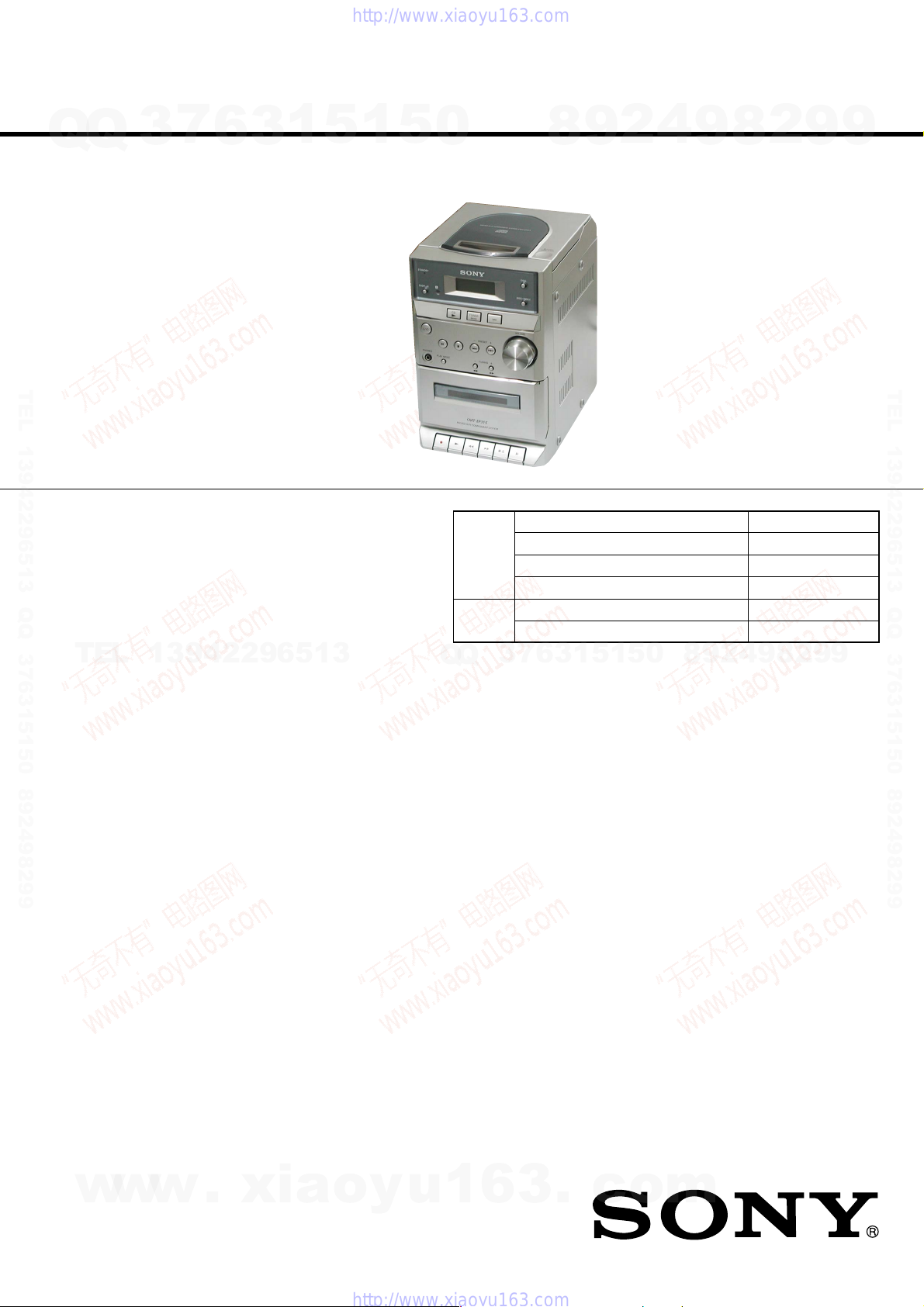
HCD-EP315 is the Amplifier, CD player, Tape
Deck and Tuner section in CMT-EP315.
Model Name Using Similar Mechanism HCD-EP313
CD
Section
TAPE
Section
CD Mechanism Type KSM-213EDP
Base Unit Name BU-K7BD44B
Optical Pick-up Name KSS-213E/C2N
Model Name Using Similar Mechanism HCD-EP313
Tape Transport Mechanism Type ADR2080FR4
8
9
2
4
9
2
8
9
AEP Model
9
TEL 13942296513 QQ 376315150 892498299
TEL
13942296513
Amplifier section
DIN power output (rated): 7 + 7 W
Continuous RMS power output (reference):
Music power output (reference):
Inputs
MD IN (phono jacks):
Outputs
PHONES (stereo minijack):
SPEAKER: Accepts impedance of 6 to
CD player section
System Compact disc and digital
LaserSemiconductor laser
Frequency response 2 Hz – 20 kHz (±0.5 dB)
(6 ohms at 1 kHz, DIN)
10 + 10 W
(6 ohms at 1 kHz, 10%
THD)
20 + 20 W
Sensitivity 500 mV,
impedance 47 kilohms
Accepts headphones with
an impedance of 8 ohms or
more
16 ohms.
audio system
(
λ
=780 nm)
Emission duration:
continuous
5
1
3
6
7
3
Q
Q
SPECIFICATIONS
Tape deck section
Recording system 4-track 2-channel stereo
Frequency response 50 – 13,000 Hz (±3 dB),
Tuner section
FM stereo, FM/AM superheterodyne tuner
FM tuner section
Tuning range 87.5 – 108.0 MHz (50-kHz
Antenna FM lead antenna
Antenna terminals 75 ohms balanced
Intermediate frequency 10.7 MHz
AM tuner section
Tuning range 531 – 1,602 kHz
Antenna AM loop antenna, exter nal
Intermediate frequency 450 kHz
using Sony TYPE I
cassettes
step)
(with the tuning interval
set at 9 kHz)
antenna terminal
8
9
4
2
9
8
0
5
1
General
Power requirements 230 V AC, 50/60 Hz
Power consumption 32 watts
Dimensions (w/h/d) Approx. 148 × 233 × 208
Mass Approx. 2.9 kg
Supplied accessories Remote (1)
Design and specifications are subject to change
witho ut notice.
0.3 watts (in the standby
mode)
mm
R6 (size AA) batteries (2)
AM loop antenna (1)
FM lead antenna (1)
2
9
9
w
w
9-877-443-03
2003H16-1
© 2003.08
w
.
xia
Sony Corporation
Home Audio Company
Published by Sony Engineering Corporation
o
y
u
MICRO HI-FI COMPONENT SYSTEM
1
6
3
.
c
o
m

HCD-EP315
TABLE OF CONTENTS
1. SERVICING NOTES ······················································· 3
Q
Q
2. GENERAL ·········································································· 5
3. DISASSEMBLY
3-1. Rear Cabinet ··································································· 7
3-2. CD Cabinet Section ························································ 8
3-3. Front Panel Section ························································· 8
3-4. CONTROL Board, BACK LIGHT Board ······················ 9
3-5. Tape Mechanism Deck (ADR2080FR4) ························· 9
3-6. Cassette Door Assy ······················································· 10
3-7. MAIN Board, POWER Board ······································ 10
3-8. CD Mechanism Deck (KSM-213EDP)························· 11
3-9. Optical Pick-up (KSS-213E/C2N) ································11
TEL 13942296513 QQ 376315150 892498299
4. MECHANICAL ADJUSTMENTS ····························· 12
5. ELECTRICAL ADJUSTMENTS ······························· 13
6. DIAGRAMS······································································ 16
6-1. Block Diagram ······························································ 17
6-2. Printed Wiring Board – CD Section – ························· 18
6-3. Schematic Diagram – CD Section – ···························· 19
6-4. Printed Wiring Board – MAIN Section
6-5. Printed Wiring Board – MAIN Section
6-6. Schematic Diagram – MAIN Section – ······················· 22
6-7. Printed Wiring Board – CONTROL Section
6-8. Printed Wiring Board – CONTROL Section
TEL
6-9. Schematic Diagram – CONTROL Section – ··············· 25
6-10. Printed Wiring Board – POWER Section – ··············· 26
6-11. Schematic Diagram – POWER Section – ·················· 27
6-12. IC Pin Function Description ······································· 30
7
3
13942296513
6
(COMPONENT SIDE) – ······· 20
(CONDUCTOR SIDE) – ······· 21
(COMPONENT SIDE) – ······· 23
(CONDUCTOR SIDE) – ······· 24
3
1
5
1
5
7. EXPLODED VIEWS
0
7-1. Overall Section ····························································· 32
7-2. Front Panel Section ······················································· 33
7-3. CD Cabinet Section ······················································ 34
7-4. Optical Pick-up Block (KSM-213EDP) ······················· 35
8. ELECTRICAL PARTS LIST······································· 36
7
3
Q
Q
8
6
3
9
1
5
2
1
5
4
0
9
8
9
8
2
4
2
9
8
9
2
9
9
TEL 13942296513 QQ 376315150 892498299
9
SAFETY-RELATED COMPONENT WARNING!!
COMPONENTS IDENTIFIED BY MARK 0 OR DOTTED LINE WITH
MARK 0 ON THE SCHEMATIC DIAGRAMS AND IN THE PARTS
LIST ARE CRITICAL TO SAFE OPERATION. REPLACE THESE
COMPONENTS WITH SONY PARTS WHOSE PART NUMBERS
w
w
APPEAR AS SHOWN IN THIS MANUAL OR IN SUPPLEMENTS
PUBLISHED BY SONY .
2
w
.
xia
o
y
u
1
6
3
.
c
o
m
SECTION 1
SERVICING NOTES
HCD-EP315
Q
TEL 13942296513 QQ 376315150 892498299
Notes on chip component replacement
Q
•Never reuse a disconnected chip component.
• Notice that the minus side of a tantalum capacitor may be damaged by heat.
Flexible Circuit Board Repairing
•Keep the temperature of the soldering iron around 270 ˚C during
repairing.
• Do not touch the soldering iron on the same conductor of the
circuit board (within 3 times).
• Be careful not to apply force on the conductor when soldering or
unsoldering.
TEL
7
3
13942296513
6
3
1
5
1
5
0
Q
Q
CAUTION
Use of controls or adjustments or performance of procedures
other than those specified herein may result in hazardous
radiation exposure.
This appliance is classified as a CLASS 1 LASER product.
The CLASS 1 LASER PRODUCT MARKING is located on
the exterior.
Laser component in this product is capable of emitting radiation
exceeding the limit for Class 1.
NOTES ON HANDLING THE OPTICAL PICK-UP
BLOCK OR BASE UNIT
The laser diode in the optical pick-up block may suffer electrostatic
break-down because of the potential difference generated by the
charged electrostatic load, etc. on clothing and the human body.
During repair, pay attention to electrostatic break-down and also
use the procedure in the printed matter which is included in the
repair parts.
The flexible board is easily damaged and should be handled with
care.
7
3
8
6
3
9
1
5
2
1
5
4
0
9
8
9
8
2
4
2
9
8
9
2
9
9
TEL 13942296513 QQ 376315150 892498299
9
NOTES ON LASER DIODE EMISSION CHECK
The laser beam on this model is concentrated so as to be focused on
the disc reflective surface by the objective lens in the optical pickup block. Therefore, when checking the laser diode emission,
observe from more than 30 cm away from the objective lens.
LASER DIODE AND FOCUS SEARCH OPERATION
CHECK
Carry out the “S curve check” in “CD section adjustment” and check
that the S curve waveforms is output three times.
w
w
w
.
xia
o
y
u
1
6
3
.
c
o
m
3
HCD-EP315
Service Position of the CD Mechanism Deck
Q
Q
3
7
6
3
1
5
1
5
0
8
9
2
4
9
8
2
9
9
TEL 13942296513 QQ 376315150 892498299
CD mechanism deck
(KSM-213EDP)
Service Position of the Tape Cassette Mechanism Deck
TEL
13942296513
Q
Q
3
7
6
3
1
5
1
5
0
8
9
2
4
9
8
2
9
TEL 13942296513 QQ 376315150 892498299
9
4
w
w
w
Tape cassette mechanism deck
(ADR2080FR4)
.
xia
o
y
u
1
6
3
.
c
o
m
Illustrati
12 3
qsq
q
qgq
SECTION 2
GENERAL
HCD-EP315
This section is extracted
from instruction manual.
7
Q
Q
TEL 13942296513 QQ 376315150 892498299
3
6
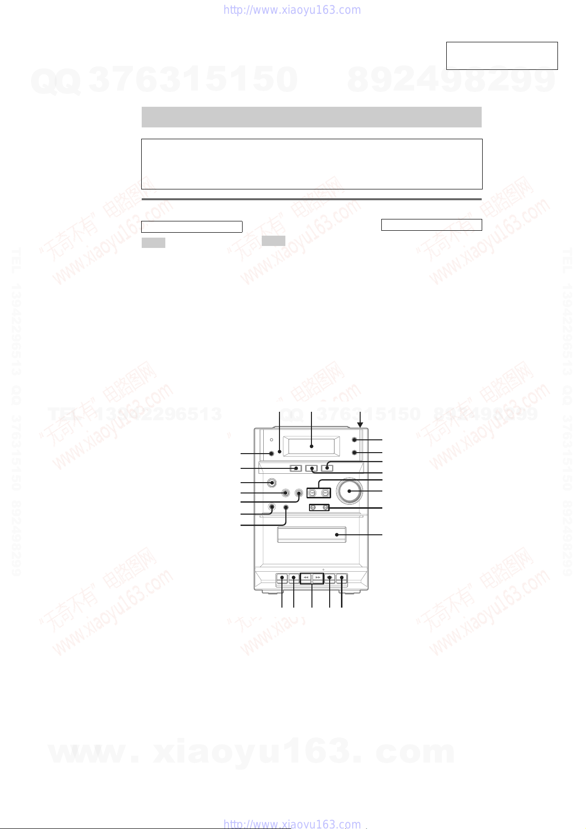
List of button locations and reference pages
How to use this page
Use this page to find the location of buttons and other
parts of the system that are mentioned in the text.
Main unit
ALPHABETICAL ORDER
A – M
BASS/TREBLE 5 (12)
Cassette compartment qa
DISPLAY wd (9, 14)
Display window 2
DSG 4 (12)
MD 6 (15)
3
1
5
1
5
0
P – Z
PHONES jack qk
PLAY MODE qj (6, 7)
PRESET +/– 8 (9)
Remote sensor 1
TUNER BAND 7 (8, 9)
TUNING +/– 0 (8, 9)
VOLUME 9 (13)
4
2
9
8
on number
r
DISPLAY wd
Name of button/part Reference page
RR
BUTTON DESCRIPTIONS
?/1 (power) wa (5, 9, 13)
m/M (fast forward/rewind)
0 (6)
./> (go back/go forward)
8 (5, 6, 7, 12, 13)
x (stop) ql (6, 7, 11, 17)
X (pause) w; (6)
CD N (play) ws (6, 7, 11)
Z PUSH OPEN/CLOSE (open/
close) 3 (6)
TAPE
m/M (fast forward/rewind)
qf (10)
xZ (stop/eject) qd (10, 11)
X (pause) qs (10, 11)
N (play) qg (10)
z (record) qh (11)
9
(9, 14)
8
2
9
9
TEL 13942296513 QQ 376315150 892498299
TEL
13942296513
wd
ws
wa
w;
ql
qk
qj
Q
h
Q
9
9
2
8
9
4
2
9
8
0
5
1
5
1
3
6
7
3
4
5
6
7
8
9
q;
qa
d
f
w
w
w
.
xia
o
y
u
1
6
3
.
c
o
m
5
HCD-EP315
Q
Q
3
Remote control
7
6
ALPHABETICAL ORDER
A – M
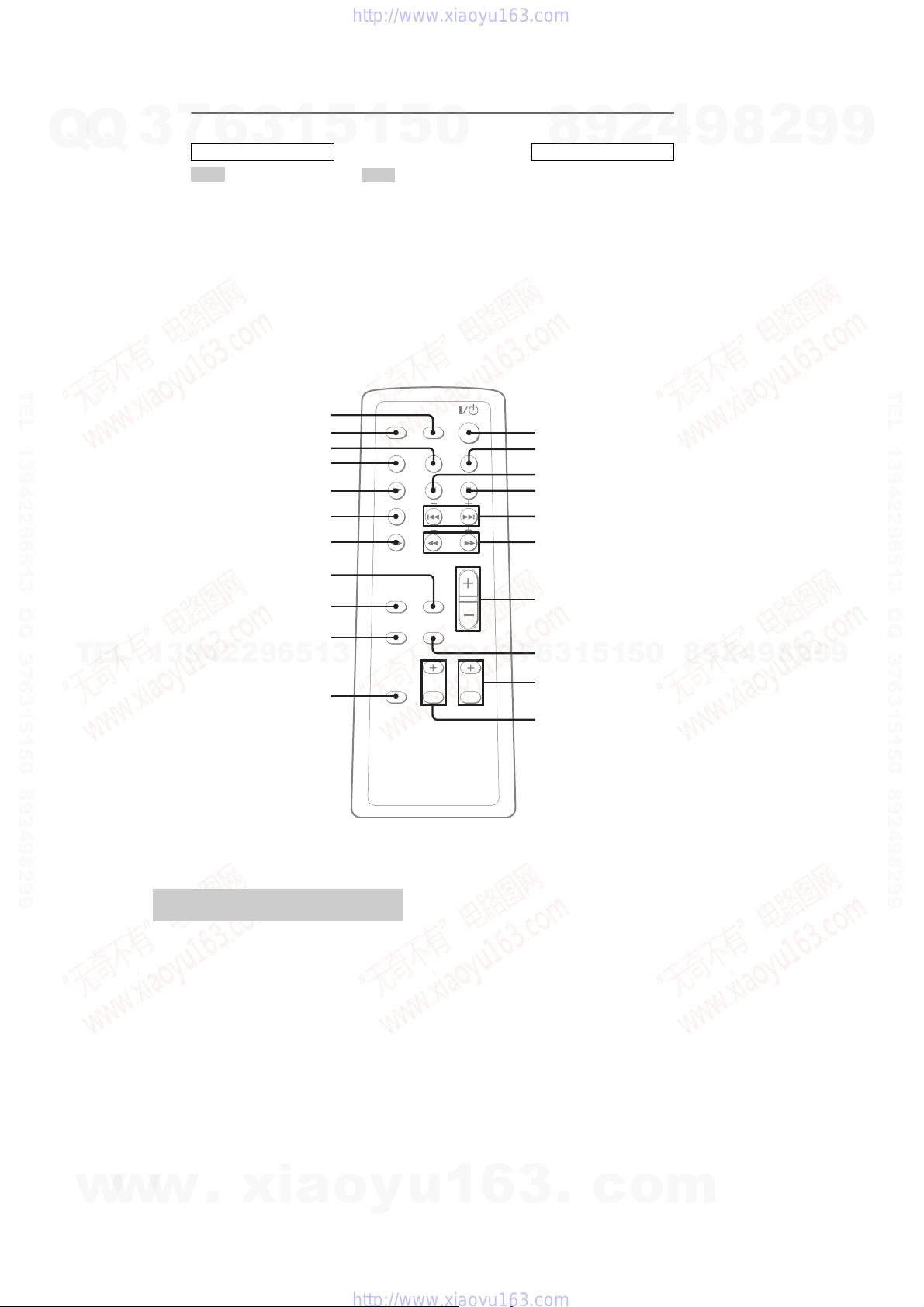
BASS +/– 0 (12)
CLEAR 8 (8, 9)
CLOCK/TIMER SELECT w;
CLOCK/TIMER SET wa (5, 13)
DISPLAY 2 (9, 14)
DSG qa (12)
MD qk (15)
3
(13)
1
5
1
5
0
P – Z
PLAY MODE/DIRECTION qd
(6, 7)
PRESET +/– 5 (9)
REPEAT/FM MODE qf (7, 9)
SLEEP ql (12)
TREBLE +/– 9 (12)
TUNER BAND qh (8, 9)
TUNER MEMORY qs (8)
TUNING +/– 6 (8, 9)
VOL +/– 7 (13)
4
2
9
8
BUTTON DESCRIPTIONS
?/1 (power) 1 (5, 9, 13)
m/M (fast forward/rewind)
6 (6)
./> (go back/go forward)
5 (5, 6, 7, 13)
x (stop) 4 (6, 7, 11, 17)
X (pause) 3 (6)
CD N (play) qj (6, 7, 11)
TAPE nN qg (10)
9
8
2
9
9
TEL 13942296513 QQ 376315150 892498299
wa
w;
ql
qk
qj
qh
qg
qf
qd
qs
TEL
13942296513
qa
Q
Q
3
7
1
2
3
4
5
6
7
8
6
9
0
3
1
5
1
5
0
8
9
2
4
9
8
2
9
TEL 13942296513 QQ 376315150 892498299
9
6
w
w
Setting the clock
Press ?/1 to turn on the system.
1
Press CLOCK/TIMER SET.
2
Press ./> repeatedly to set the
3
hour.
Press CLOCK/TIMER SET.
4
Press ./> repeatedly to set the
5
minute.
Press CLOCK/TIMER SET.
6
The clock starts working.
To adjust the clock
Press CLOCK/TIMER SET.
1
Press ./> to select the clock display,
2
then press CLOCK/TIMER SET.
w
3
.
xia
Do the same procedures as step 3 to 6
above.
o
y
u
1
6
3
.
c
o
m
)
Q
• This set can be disassembled in the order shown below.
Q
7
3
CD CABINET SECTION
6
SET
REAR CABINET
3
1
5
1
SECTION 3
DISASSEMBLY
5
0
8
9
2
4
8
9
CD MECHANISM DECK
(KSM-213EDP)
HCD-EP315
2
9
9
TEL 13942296513 QQ 376315150 892498299
Note: Follow the disassembly procedure in the numerical order given.
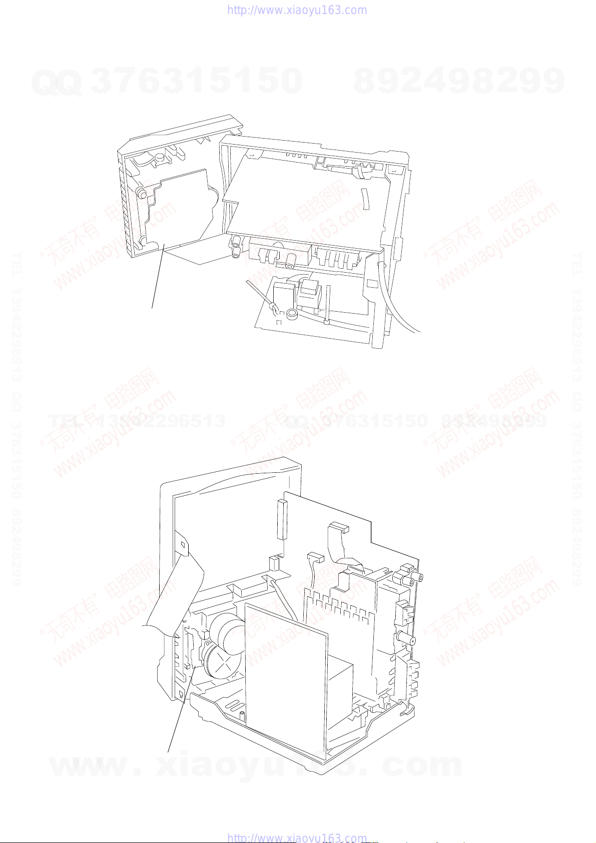
3-1. Rear Cabinet
TEL
FRONT PANEL SECTION
CONTROL BOARD,
BACK LIGHT BOARD
13942296513
TA PE MECHANISM DECK
(ADR2080FR4)
CASSETTE DOOR ASSY
3
Q
Q
7
6
1
3
6
rear cabinet
MAIN BOARD,
POWER BOARD
0
5
1
5
OPTICAL PICK-UP
(KSS-213E/C2N)
9
4
2
9
8
3
five screws
(+BVTP 3
2
9
2
8
×
8)
three screws
(+BTP 3
1
×
two screws
(+BVTP 3
9
8)
TEL 13942296513 QQ 376315150 892498299
×
8
w
w
w
.
xia
5
four screws
(+KTP 3
o
y
×
12)
u
1
6
3
.
c
o
4
four screws
(+KTP 3
m
×
12)
7
HCD-EP315
)
3-2. CD Cabinet Section
7
Q
Q
3
6
3
1
screw
1
6
connector
(+BVTP 3
5
1
5
0
7
CD cabinet section
2p (CN101)
×
8)
5
8
9
2
4
9
8
2
9
9
TEL 13942296513 QQ 376315150 892498299
4
two claws
3
two claws
TEL
3-3. Front Panel Section
13942296513
4
connector 30p
(CN202) (board to board)
3
8
front panel section
screw
(+BTP 3
×
5
8)
connector
7p (CN502)
Q
Q
3
7
6
3
2
w
21p (CN101)
5
1
ire (flat type)
0
5
1
8
2
9
1
two screws
8
9
4
(+BVTP 3
×
2
10
9
TEL 13942296513 QQ 376315150 892498299
9
8
w
w
w
2
two claws
.
xia
7
6
connector
8p (CN501)
o
y
u
1
6
3
.
c
o
m
Q
3-4. CONTROL Board, BACK LIGHT Board
Q
3
7
6
3
1
5
1
5
0
3
8
nine screws
(+BVTP 3 × 8)
2
9
5
CONTROL board
4
4
9
w
ire (flat type)
21p (CN301)
HCD-EP315
2
8
9
9
TEL 13942296513 QQ 376315150 892498299
2
1
volume knob
TEL
13942296513
3-5. Tape Mechanism Deck (ADR2080FR4)
screw
(+BVTP 3 × 10)
Q
Q
3
7
6
3
1
5
8
BACK LIGHT
board
5
1
3
6
two claws
7
9
8
0
two screws
(+BVTP 3 × 10)
connector
2p (CN305)
9
4
2
8
2
9
TEL 13942296513 QQ 376315150 892498299
9
w
w
1
w
Open the cassette door.
.
xia
4
tape mechanism deck
(ADR2080FR4)
o
y
u
1
6
3
.
c
o
2
screw
(+BVTP 3 × 10)
m
9
HCD-EP315
3-6. Cassette Door Assy
7
Q
Q
3
6
1
3
2
cassette door assy
5
1
5
0
8
9
2
4
9
8
2
9
9
TEL 13942296513 QQ 376315150 892498299
1
two claws
3-7. MAIN Board, POWER Board
TEL
2
13942296513
screw
(+BVTP 3
3
×
8)
MAIN board
6
shield plate trans
Q
Q
5
7
3
four screws
(+BVTP 4 × 12)
6
3
1
5
1
5
0
8
9
2
4
9
8
2
9
TEL 13942296513 QQ 376315150 892498299
9
10
w
w
w
.
xia
1
connector
6p (CN901)
7
o
y
u
1
6
3
two cushions
.
8
c
4
PT PWB cover
POWER board
o
m
Q
3-8. CD Mechanism Deck (KSM-213EDP)
Q
3
7
6
3
1
5
1
5
0
6
two cushion
rubbers
8
9
2
4
three claws
4
5
panel CD
9
HCD-EP315
2
8
3
two screws
(+PWH 2.6
q;
w
ire (flat type)
16p (CN102)
9
×
10)
9
TEL 13942296513 QQ 376315150 892498299
qs
CD mechanism deck
(KSM-213EDP)
2
TEL
13942296513
3-9. Optical Pick-up (KSS-213E/C2N)
6
optical pick-up
(KSS-213E/C2N)
two screws
(+PWH 2.6
8
four remove soldrings.
qa
CD board
×
10)
Q
Q
3
7
6
3
1
5
1
5
2
9
1
0
gear (A)
screw
×
5)
(+P 2
CD deck cover
4
2
9
8
9
7
8
two cushion
rubbers
9
9
2
TEL 13942296513 QQ 376315150 892498299
w
w
w
5
.
xia
sled shaft
o
y
u
1
6
3
.
1
c
claw
o
4
3
m
11
HCD-EP315
SECTION 4
MECHANICAL ADJUSTMENTS
Precaution
1. Clean the following parts with a denatured alcohol-moistened
Q
Q
swab:
record/playback heads pinch rollers
erase head rubber belts
capstan idlers
2. Demagnetize the record/playback head with a head demagnetizer.
3. Do not use a magnetized screwdriver for the adjustments.
4. After the adjustments, apply suitable locking compound to the
parts adjusted.
5. The adjustments should be performed with the rated power
supply voltage unless otherwise noted.
Torque Measurement
3
7
6
3
1
5
1
5
0
8
9
2
4
9
8
2
9
9
TEL 13942296513 QQ 376315150 892498299
Mode
FWD
FWD
back tension
REV
REV
back tension
FF/REW
FWD tension
TEL
REV tension
Torque meter Meter reading
2.94 – 7.84 mN • m
CQ-102C
CQ-102C
CQ-102RC
CQ-102RC
CQ-201B
CQ-403A
13942296513
CQ-403R
(30 to 79 g • cm)
(0.42 – 1.11 oz • inch)
0.15 – 0.59 mN • m
(2 to 6 g • cm)
(0.03 – 0.08 oz • inch)
0.15 – 0.59 mN • m
(2 to 6 g • cm)
(0.03 – 0.08 oz • inch)
0.15 – 0.59 mN • m
(2 to 6 g • cm)
(0.03 – 0.08 oz • inch)
6.86 – 17.64 mN • m
(70 to 179 g • cm)
(0.98 – 2.49 oz • inch)
9.8 mN • m or more
(100 g • cm or more)
(1.4 oz • inch or more)
9.8 mN • m or more
(100 g • cm or more)
(1.4 oz • inch or more)
Q
Q
3
7
6
3
1
5
1
5
0
8
9
2
4
9
8
2
9
TEL 13942296513 QQ 376315150 892498299
9
12
w
w
w
.
xia
o
y
u
1
6
3
.
c
o
m
)
SECTION 5
ELECTRICAL ADJUSTMENTS
HCD-EP315
DECK SECTION 0 dB=0.775V
7
Q
Q
TEL 13942296513 QQ 376315150 892498299
TEL
3
1. Demagnetize the record/playback head with a head demagnetizer.
2. Do not use a magnetized screwdriver for the adjustments.
3. After the adjustments, apply suitable locking compound to the
parts adjusted.
4. The adjustments should be performed with the rated power
supply voltage unless otherwise noted.
5. The adjustments should be performed in the order given in this
service manual. (As a general rule, playback circuit adjustment
should be completed before performing recording circuit
adjustment.)
6. The adjustments should be performed for both L-CH and RCH.
7. Switches and controls should be set as follows unless otherwise
specified.
P-4-A100
WS-48B
[Record/Playback Head Azimuth Adjustment]
Procedure:
1. Mode : Playback
test tape
P-4-A100
(10kHz, –10dB)
13942296513
2. Turn the adjustment screw and check output peaks. If the peaks
do not match for L-CH and R-CH, turn the adjustment screw
so that outputs match within 1 dB of peak.
6
10 kHz, –10 dB
set
1
3
Signal Used forTape
3 kHz, 0 dB
MAIN board
J203
speaker terminal
5
1
5
Azimuth Adjustment
Tape Speed Adjustment
level meter
+
–
0
Q
Q
3. Mode: Playback
test tape
P-4-A100
(10kHz, –10dB)
4. After the adjustments, apply suitable locking compound to the
Adjustment Location: Record/Playback/Erase Head
[Tape Speed Check]
Procedure:
1. Turn the power on.
2. Insert the WS-48B into deck.
3. Press the N button of deck.
4. Check the reading of frequency counter becomes 3000 ± 90 Hz.
7
3
Sample Value of Wow and flutter
Adjustment Location: Record/Playback Head.
4
2
9
8
set
Waveform of oscilloscope
5
°
good
0
in phase 45
parts adjusted.
1
5
1
3
6
W.RMS (JIS) less than 0.3%
(test tape: WS-48B)
8
9
MAIN board
J203
speaker terminal
L
R
135
90
°
4
2
9
8
2
°
9
9
oscilloscope
180
wrong
2
8
°
9
9
TEL 13942296513 QQ 376315150 892498299
9
L-CH
peak
w
w
screw
position
R-CH
peak
w
output
level
.
xia
within
1 dB
L-CH
peak
within 1dB
u
screw
position
1
6
3
R-CH
peak
o
y
adjustment screw
.
c
o
m
Note: Refer to “3-6. Cassette Door Assy” (see page 10
13
HCD-EP315
+
–
CD board
TP (RFAC)
TP (VC)
oscilloscope
CD SECTION
Q
Q
Note:
1. CD Block is basically designed to operate without adjustment. Therefore, check each item in order given.
2. Use YEDS-18 disc (3-702-101-01) unless otherwise indicated.
3. Use an oscilloscope with more than 10MΩ impedance.
4. Clean the object lens by an applicator with neutral detergent when the
signal level is low than specified value with the following checks.
S-curve Check
Connection:
TEL 13942296513 QQ 376315150 892498299
Procedure:
1. Connect an oscilloscope to test point TP (FE) and TP (DVC)
on the CD board.
2. Turn the power on.
3. Put the disc (YEDS-18) in and turned power switch on again
and actuate the focus search. (actuate the focus search when
disc table is moving in and out)
4. Check the oscilloscope waveform (S-curve) is symmetrical
between A and B. And confirm peak to peak level within 2 ± 1
Vp-p.
S-curve waveform
TEL
7
3
CD board
TP (FE)
TP (DVC)
6
1
3
oscilloscope
+
–
symmetry
13942296513
A
B
within 2
5
1
±
1 Vp-p
5
RFDC signal waveform
0
Checking Location: CD board (Conductor side)
RFAC Level Check
Connection:
Procedure:
1. Connect an oscilloscope to test point TP (RFAC) and TP (VC)
on the CD board.
2. Turn the power on.
3. Put the disc (YEDS-18) in to playback the number five track.
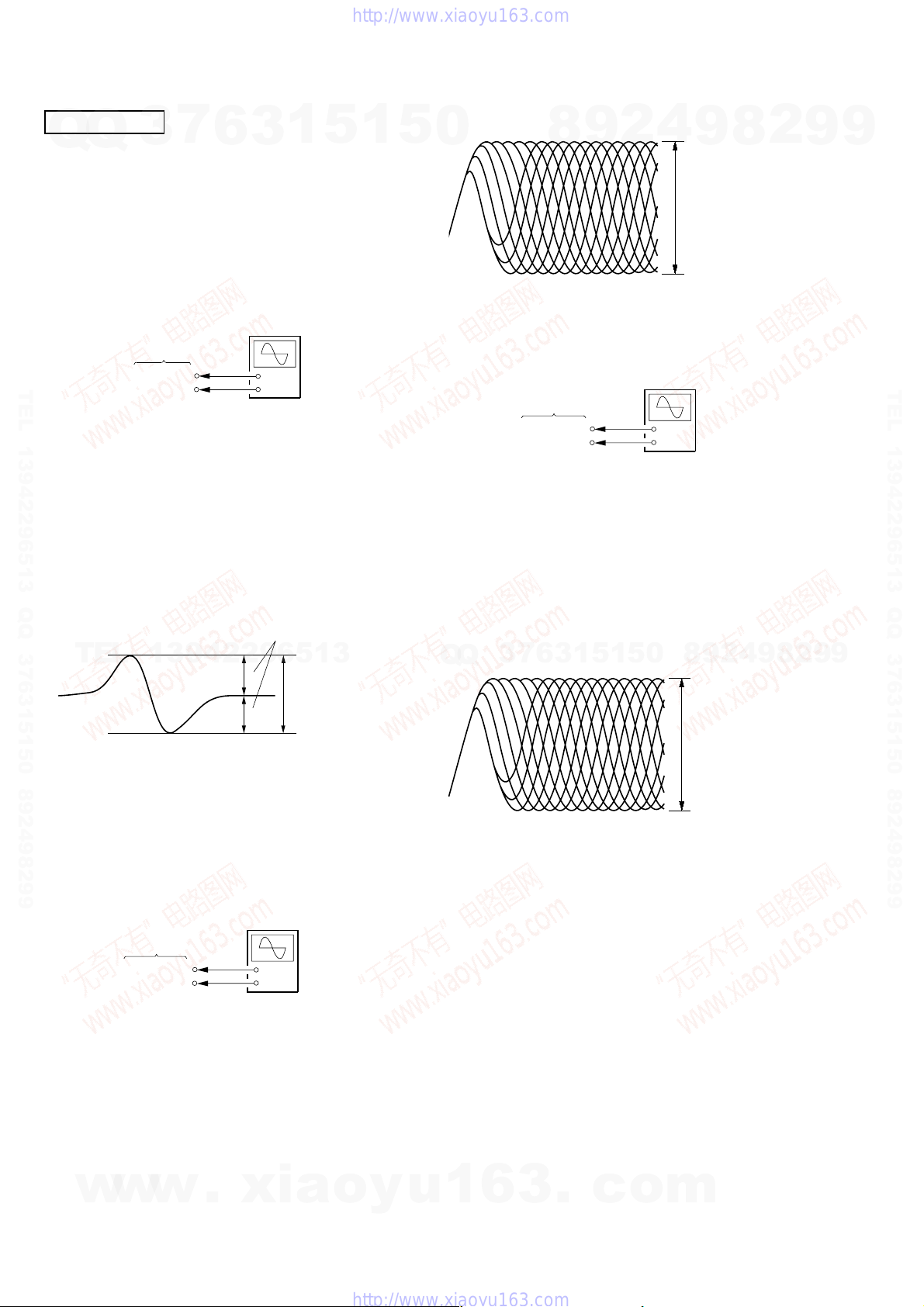
4. Confirm that oscilloscope waveform is clear and check RFAC
signal level is correct or not.
Note: A clear RFAC signal waveform means that the shape “◊” can be
clearly distinguished at the center of the waveform.
RFAC signal waveform
Q
Q
3
7
8
6
3
9
1
5
2
1
5
VOLT/DIV: 200 mV
4
9
TIME/DIV: 500 ns
level: 0.7
8
0
2
8
±
0.2 Vp-p
8
9
4
2
9
VOLT/DIV: 200 mV
TIME/DIV: 500 ns
9
2
9
9
TEL 13942296513 QQ 376315150 892498299
9
Note: •Try to measure several times to make sure than the ratio of A : B
Checking Location: CD board (Conductor side)
RFDC Level Check
Connection:
Procedure:
1. Connect an oscilloscope to test point TP (RFDC) and TP (DVC)
2. Turn the power on.
3. Put the disc (YEDS-18) in to playback the number five track.
4. Confirm that oscilloscope waveform is clear and check RFDC
Note: A clear RFDC signal waveform means that the shape “◊” can be
or B : A is more than 10 : 7.
•Take sweep time as long as possible and light up the
brightness to obtain best waveform.
oscilloscope
CD board
TP (RFDC)
TP (DVC)
on the CD board.
signal level is correct or not.
clearly distinguished at the center of the waveform.
+
–
level: 0.9
Checking Location: CD board (Conductor side)
±
0.4 Vp-p
w
14
w
w
.
xia
o
y
u
1
6
3
.
c
o
m
 Loading...