

Page 1
HCD-ED1
SERVICE MANUAL
Ver 1.1 2001. 06
With SUPPLEMENT-1
(9-922-706-81)
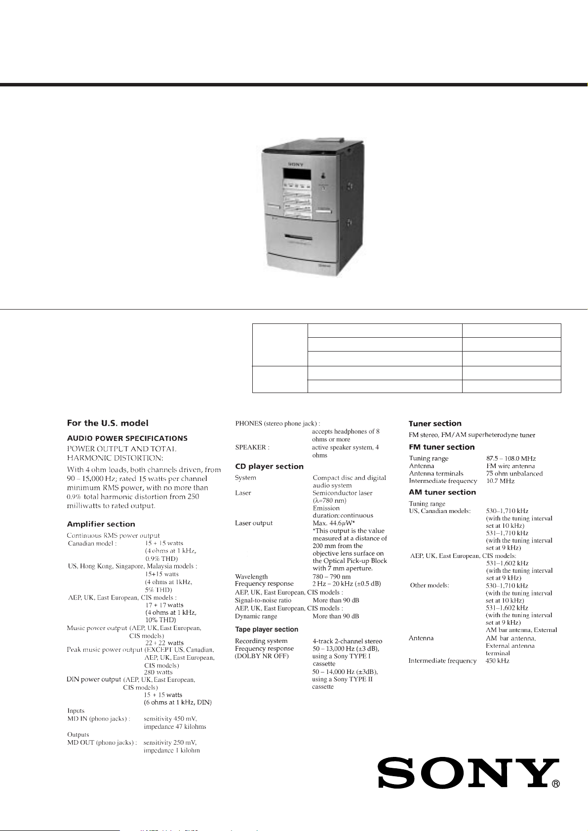
HCD-ED1 is the tuner, deck, CD and
amplifier section in CMT-ED1.
This stereo system is equipped with the Dolby* Btype noise reduction system.
*Dolby noise reduction manufactured under license
from Dolby Laboratories Licensing Corporation.
“DOLBY” and the double-D symbol a are trademarks of Dolby Laboratories Licensing Corporation.
CD
SECTION
T APE
DECK
SECTION
Model Name Using Similar Mechanism NEW
Base Unit Type BU17-BD19
Optical Pick-up Type KSS-213BA/S-N
Model Name Using Similar Mechanism NEW
T ape T r ansport Mechanism T ype CMAL2Z076A
US Model
Canadian Model
AEP Model
UK Model
E Model
SPECIFICA TIONS
— Continued on next page —
9-922-706-12
2001F0200-1
© 2001.6
COMPACT DISC DECK RECEIVER
Sony Corporation
Home Audio Company
Shinagawa Tec Service Manual Production Group
– 1 –
Page 2
CAUTION
AC
voltmeter
(0.75V)
1.5k
Ω
0.15µF
Parts on Set
Earth Ground
Use of controls or adjustments or performance of procedures
other than those specified herein may result in hazardous radiation exposure.
Notes on chip component replacement
• Never reuse a disconnected chip component.
• Notice that the minus side of a tantalum capacitor may be
damaged by heat.
SAFETY CHECK-OUT
After correcting the original service problem, perform the following safety checks before releasing the set to the customer:
Check the antenna terminals, metal trim, “metallized” knobs, screws,
and all other exposed metal parts for A C leakage. Check leakage as
described below.
LEAKAGE
The AC leakage fr om any exposed metal part to earth Ground and
from all exposed metal parts to any exposed metal part having a
return to chassis, must not exceed 0.5 mA (500 microampers). Leakage current can be measured by any one of three methods.
1. A commercial leakage tester, such as the Simpson 229 or RCA
WT-540A. Follow the manufacturers’ instructions to use these
instruments.
2. A battery-operated AC milliammeter. The Data Precision 245
digital multimeter is suitable for this job.
3. Measuring the voltage drop across a resistor by means of a VOM
or battery-operated AC voltmeter. The “limit” indication is 0.75
V, so analog meters must have an accurate low-voltage scale.
The Simpson 250 and Sanwa SH-63Trd are examples of a passive VOM that is suitable. Nearly all battery operated digital
multimeters that have a 2V AC range are suitable. (See Fig. A)
Flexible Circuit Board Repairing
• Keep the temperature of soldering iron around 270˚C
during repairing.
• Do not touch the soldering iron on the same conductor of the
circuit board (within 3 times).
• Be careful not to apply force on the conductor when soldering
or unsoldering.
Laser component in this product is capable of emitting radiation
exceeding the limit for Class 1.
This appliance is classified as
a CLASS 1 LASER product.
The CLASS 1 LASER PRODUCT MARKING is located on
the rear exterior.
This caution
label is located
inside the unit.
Fig. A. Using an AC voltmeter to check AC leakage.
SAFETY-RELATED COMPONENT WARNING !!
COMPONENTS IDENTIFIED BY MARK ! OR DOTTED LINE
WITH MARK ! ON THE SCHEMATIC DIAGRAMS AND IN
THE PARTS LIST ARE CRITICAL TO SAFE OPERATION.
REPLACE THESE COMPONENTS WITH SONY PARTS
WHOSE PART NUMBERS APPEAR AS SHOWN IN THIS
MANUAL OR IN SUPPLEMENTS PUBLISHED BY SONY.
ATTENTION AU COMPOSANT AYANT RAPPORT
À LA SÉCURITÉ!!
LES COMPOSANTS IDENTIFIÉS PAR UNE MARQUE ! SUR
LES DIAGRAMMES SCHÉMATIQUES ET LA LISTE DES
PIÈCES SONT CRITIQUES POUR LA SÉCURITÉ DE
FONCTIONNEMENT. NE REMPLA CER CES COMPOSANTS
QUE PAR DES PIÈCES SONY DONT LES NUMÉROS
SONT DONNÉS DANS CE MANUEL OU DANS LES
SUPPLÉMENTS PUBLIÉS PAR SONY.
– 2 –
Page 3
SERVICING NOTE
TABLE OF CONTENTS
NOTES ON HANDLING THE OPTICAL PICK-UP BLOCK
OR BASE UNIT
The laser diode in the optical pick-up block may suffer electrostatic
break-down because of the potential difference g enerated by the
charged electrostatic load, etc. on clothing and the human body.
During repair, pay attention to electrostatic break-down and also
use the procedure in the printed matter which is included in the
repair parts.
The flexible board is easily damaged and should be handled with
care.
NOTES ON LASER DIODE EMISSION CHECK
The laser beam on this model is concentrated so as to be focused on
the disc reflective surface by the objective lens in the optical pickup block. Therefore, when checking the laser diode emission, observe from more than 30 cm away from the objective lens.
1. GENERAL .......................................................................... 4
2. DISASSEMBLY
2-1. CD Door, CD Base and Base Unit........................................ 6
2-2. Rear Panel ........................................................................... 6
2-3. Bottom Cover and Front Panel Block ................................... 7
2-4. Door Cover Assy and Mechanical Deck (Cassette) .............. 7
3. MECHANICAL ADJUSTMENTS ............................... 8
4. ELECTRICAL ADJUSTMENTS ................................. 8
5. DIAGRAMS
5-1. Circuit Boards Location...................................................... 13
5-2. IC Pin Function ...................................................................14
5-3. Schematic Diagram — CD Section — ............................... 16
5-4. Printed Wiring Board — CD Section — ............................. 19
5-5. Schematic Diagram — Input/Output Section — ................ 21
5-6. Printed Wiring Board — Input/Output Section — .............. 23
5-7. Printed Wiring Board — Deck Section — .......................... 25
5-8. Schematic Diagram — Deck Section — ............................ 27
5-9. Schematic Diagram — Display Section — ........................ 30
5-10. Printed Wiring Board — Display Section — ................... 33
5-11. Schematic Diagram — Power Section — ........................ 36
5-12. Printed Wiring Board — Power Section — ..................... 39
5-13. IC Block Diagrams ........................................................... 41
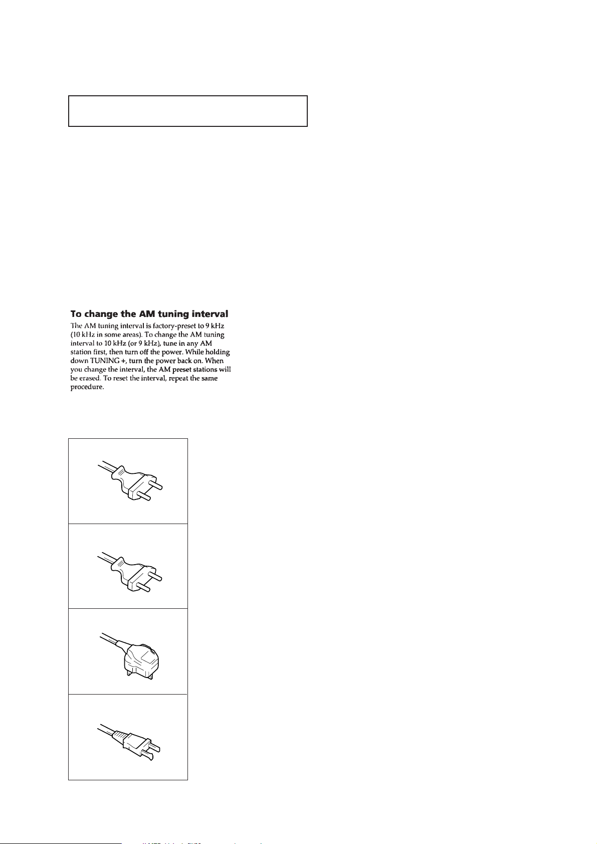
MODEL IDENTIFICATION
— AC POWER SUPPLY CODE —
AEP, East European, CIS model
(Without voltage selector)
Singapore, Malaysia,
Hong Kong model
(With voltage selector)
UK model
6. EXPLODED VIEWS
6-1. CD Section ......................................................................... 45
6-2. Rear Panl Section................................................................ 46
6-3. Front Panel Section ............................................................. 47
6-4. Mechanism Deck Section (Cassette) .................................. 48
6-5. Base Unit Section (BU17-BD19)........................................ 49
7. ELECTRICAL PARTS LIST ........................................ 50
US, Canadian model
– 3 –
Page 4
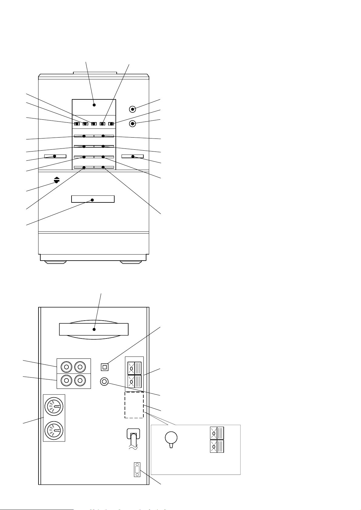
Location of Parts and Controls
FRONT PANEL
1
2
3
4
5
6
7
8
9
20
SECTION 1
GENERAL
19
18
17
16
15
14
13
1 Displa y windo w
2 DBFB lamp
3 CD SYNC lamp
4 REC lamp
5 ª button
6 BAND FM ∏ button
7 POWER b utton
8 TUNING ≠ º – button
9 § button (Push open)
1 0 V OLUME – b utton
1 1 DECK Lid
1 2 VOLUME + button
1 3 TUNING ‚± + button
14 FUNCTON b utton
1 5 BAND AM π button
16 · button
17 SOUND MODE b utton
1 8 WIDE lamp
19 Remote sensor
2 0 NEAR F. lamp
10
11
REAR PANEL
2
3
12
1
1 AM ANTENNA
2 MD IN jacks
9
8
3 MD OUT jacks
4 SPEAKER jacks
5 V OLT AGE SELECT OR s witc h
(Malaysia, Singapore , Hong K ong models onl y)
6 FM ANTENNA terminal
7 PHONES jack
8 AM ANTENNA terminals
9 OPTICAL terminal
7
6
4
AEP,UK,
East European
,CIS model
US,Canadian,
Singapore,Malaysia,
Hong Kong model
5
– 4 –
Page 5
REMOTE
1
10
20
2
19
3
4
5
6
18
17
16
15
14
7
8
13
12
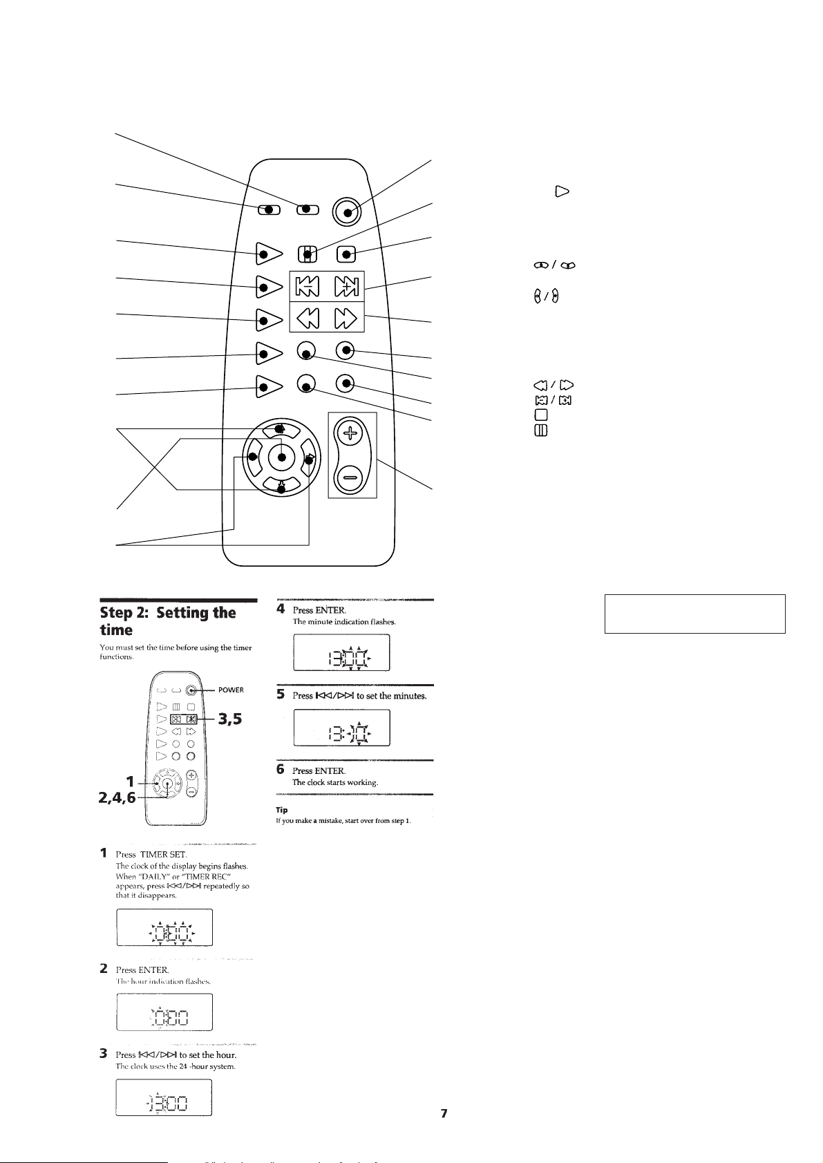
1 DISPLAY button
2 DBFB b utton
3 CD b utton
4 TUNER/BAND button
5 TAPE œ button
6 DIR MODE button
7 CD REPEA T button
8 b uttons
9 ON/OFF b utton
1 0 b uttons
1 1 VOL (+/–) b utton
12 STEREO/MONO b utton
1 3 TUNING/PLAY MODE button
14 DOLBY NR b utton
15 r REC b utton
1 6 (re wind/fast f orwar d) b uttons
1 7 AMS* b uttons
18 (stop) b utton
19 (pause) b utton
20 POWER s witc h
*AMS=Auto Music Sensor
11
9
This section is extracted from
instruction manual.
– 5 –
Page 6

DISASSEMBLY
Note: Follo w the disassemb ly pr ocedure in the n umerical or der given.
2-1. CD DOOR, CD BASE AND BASE UNIT
5
Two hook screws
7
Three screws (K3x8)
!¡
CD base
6
Three screws (K3x8)
SECTION 2
2
Bar rubber
1
4
Hinge spring
9
Three screws (K3x8)
8
Two hook screws
Open the CD door.
3
Hinge pin
2-2. REAR PANEL
5
!∞
Side bracket
Two springs
(compression)
!£
!¢
Two washers
!º
Three screws (K3x8)
!ª
Base unit
!•
Two springs (compression)
!¶
Two washers
!§
Two screws (TPG P2x8)
!™
Wire (Flat type)
Two screws (TPG P2x8)
7
Rear panel
1
Two screws
(BVTP 3x10)
2
Screw
(BVTP 3x8)
3
Two screws
(BVTP 3x8)
– 6 –
6
Side bracket
4
Three screws
(BVTP 3x8)
Page 7
2-3. BOTTOM COVER AND FRONT PANEL BLOCK
r
k
5
Front panel block
4
Two claws
1
Two screws
(BVTP 3x8)
3
2
Two screws
(BVTP 3x8)
Bottom cove
2-4. DOOR COVER ASSY AND MECHANICAL DECK (CASSETTE)
A
3
Door spring
1
Open the Door cover ASSY. (Push the A portion.)
2
Door cover assy
4
Four screws
(BVTP 3x10)
5
Mechanical dec
(cassette)
– 7 –
Page 8
SECTION 3
MECHANICAL ADJUSTMENTS
SECTION 4
ELECTRICAL ADJUSTMENTS
PRECAUTION
1. Clean the following parts with a denatured alcohol-moistened
swab :
record/playback heads pinch rollers
erase head rubber belts
capstan idlers
2. Demagnetize the record/playback head with a head demagnetizer.
3. Do not use a magnetized screwdriver for the adjustments.
4. After the adjustments, apply suitable locking compound to the
parts adjusted.
5. The adjustments should be performed with the rated power supply voltage unless otherwise noted.
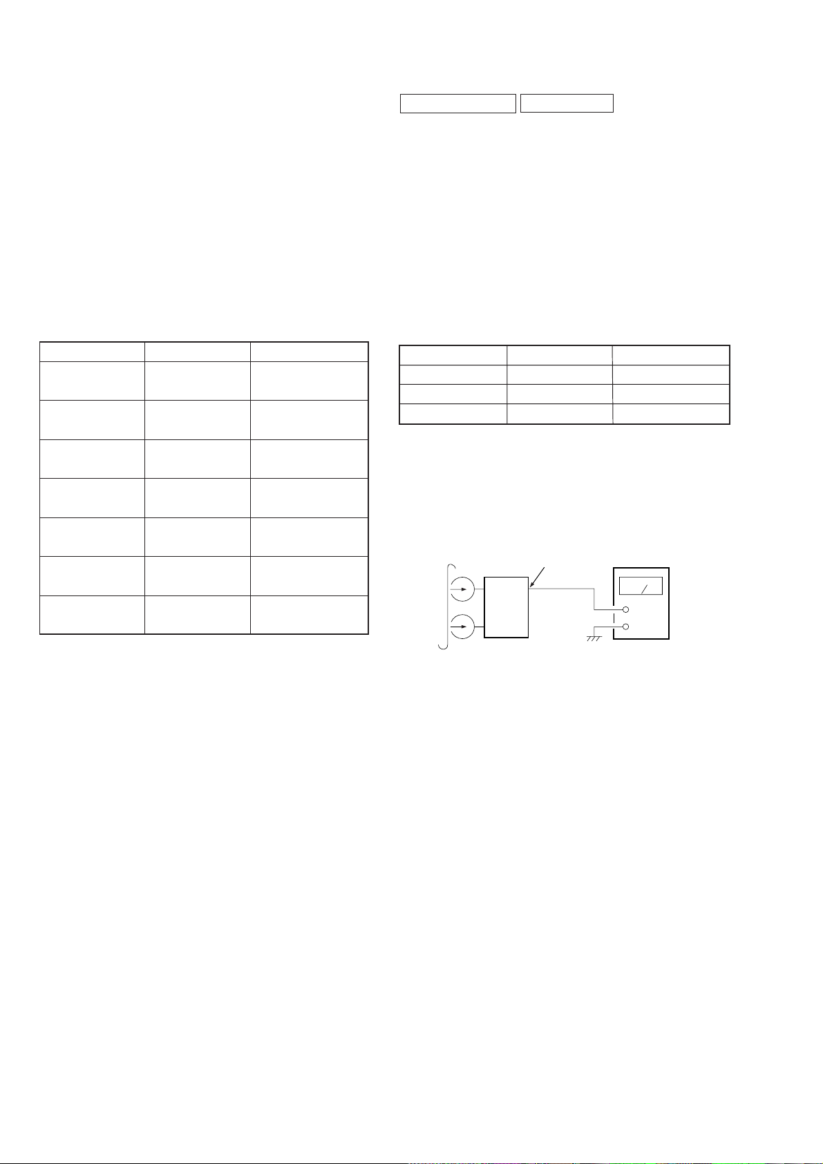
Torque Measurement
Torque Torque meter
FWD
FWD
back tension
REV
REV
back tension
FF/REW
FWD tension
CQ-102C
CQ-102C
CQ-102RC
CQ-102RC
CQ-201B
CQ-403A
Meter reading
28 to 71g • cm
(0.39 – 0.99 oz • inch)
1 to 7g • cm
(0.01 – 0.10 oz • inch)
28 to 71g • cm
(0.39 – 0.99 oz • inch)
1 to 7g • cm
(0.01 – 0.10 oz • inch)
56 to 122g • cm
(0.78 – 1.69 oz • inch)
100g or more
(3.53 oz or more)
DECK SECTION 0 dB=0.775V
1. Demagnetize the record/playback head with a head damagnetizer.
(Do not bring the head demagnetizer close to the erase head.)
2. Do not use a magnetized screwdriver for the adjustments.
3. After the adjustments, apply suitable locking compound to the
parts adjusted.
4. The adjustments should be performed with the rated power supply voltage unless otherwise noted.
5. The adjustments should be performed in the order given in this
service manual. (As a general rule, playback circuit adjustment
should be completed before performing recording circuit adjustment.)
6. The adjustments should be performed for both L-CH and R-ch.
7. Switches and controls should be set as follows unless otherwise
specified.
Tape
P-4-A100
WS-48B
P-4-L300
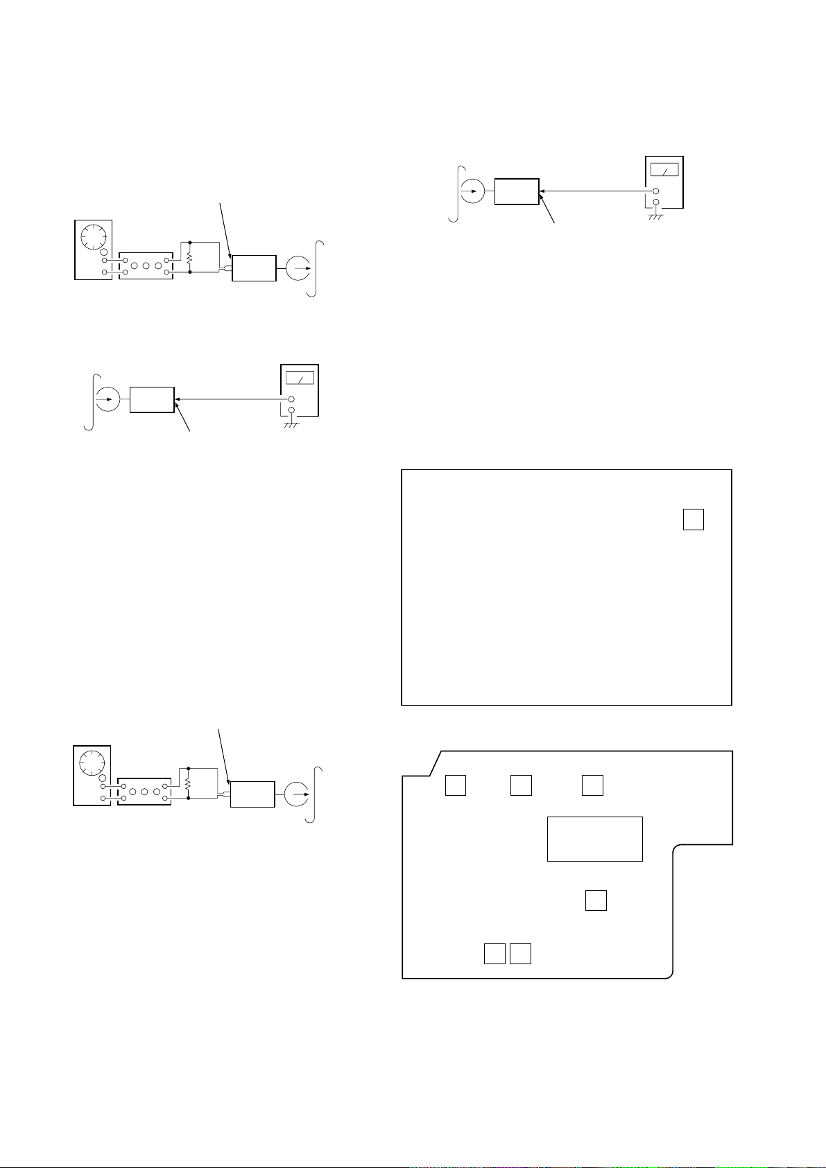
Record/Playback Head Azimuth Adjustment
Procedure :
1. Mode : Playback
test tape
P-4-A100
(10kHz, –10dB)
Signal
10 kHz, –10 dB
3 kHz, 0 dB
315 Hz, 0 dB
MD OUT (JK301)
Used for
Azimuth Adjustment
Tape Speed Adjustment
Level Adjustment
level meter
REV tension
CQ-403R
100g or more
(3.53 oz or more)
set
+
–
– 8 –
Page 9
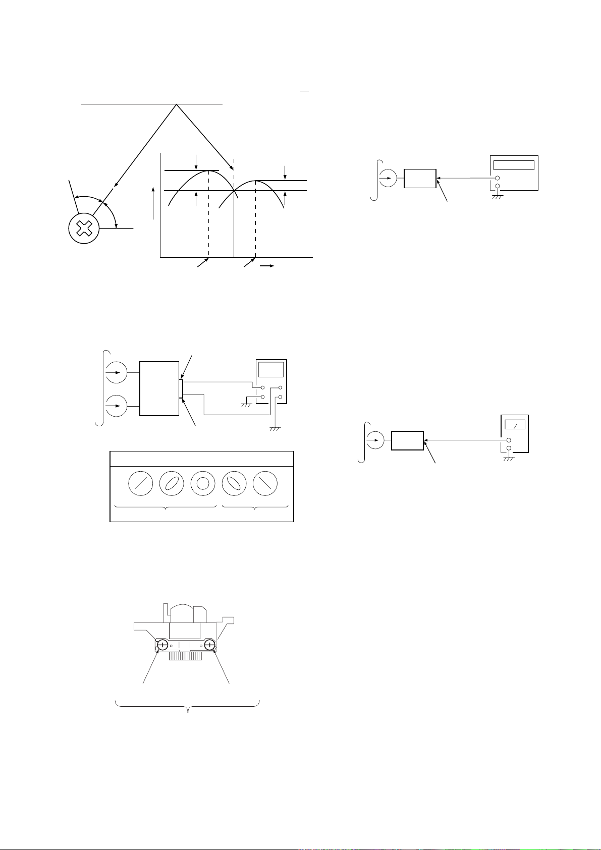
2. Turn the adjustment scre w and check output peaks. If the peaks
r
r
do not match for L-CH and R-CH, turn the adjustment screw so
that outputs match within 1 dB of peak.
L-CH
peak
output
level
within
1dB
within 1dB
Tape Speed Adjustment
Procedure :
Mode : Playback
test tape
WS-48B
(3kHz, 0dB)
set
frequency counte
+
–
MD OUT (JK301)
R-CH
screw
position
peak
L-CH
peak
R-CH
peak
screw
position
3. Mode : Playback
test tape
P-4-A100
(10kHz, –10dB)
in phase
MD OUT (JK301)
L
set
R
MD OUT (JK301)
Waveform of oscilloscope
45
°
90
°
good
135
oscilloscope
°
180
wrong
°
4. After the adjustments, apply suitable locking compound to the
parts adjusted.
1. Insert the WS-48B into the deck, and playback.
2. Adjust the VR770/RELAY board so that the frequency counter
reading becomes 3000 ± 90 Hz.
Adjustment Location : RELAY board
Sample Value of Wow and flutter
W.RMS (JIS) less than 0.3%
(test tape: WS-48B)
Playback Level Adjustment
Procedure :
Mode : Playback
test tape
P-4-L300
(315Hz, 0dB)
set
MD OUT (JK301)
level mete
Deck is VR703 (L-CH) and VR704 (R-CH)
so that adjustment within the following adjustment level.
Adjustment level :
Playback level: 301.5 to 338.3 mV (–8.2 to –7.2 dB) level difference between the channels: within ±0.5 dB
Adjustment Location : TAPE PREAMP board
Adjustment Location :
FWD side
Adjustment screw
REV side
– 9 –
Page 10
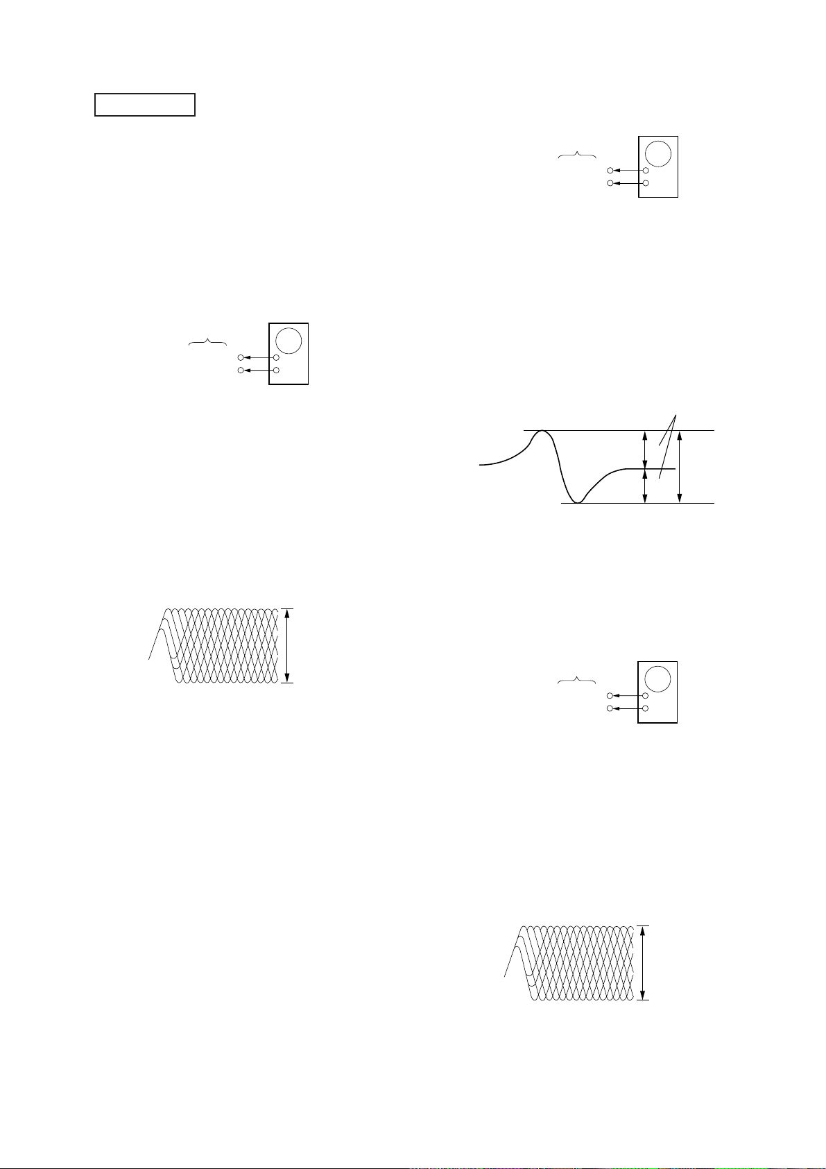
Record Bias Adjustment
r
r
2. Mode: Playback
Procedure :
1. Mode : Record
MD IN (JK301)
1) 315Hz
2) 10kHz
AF OSC
600
attenuator
}
50 mV (–23.8 dB)
Ω
blank tape
CS-123
set
2. Mode : Playback
recorded
position
set
MD OUT (JK301)
level mete
Confirm playback the signal recorded in step 1 become adjustment
level as follows.
If these levels do not adjustment level, adjustment the VR701 (LCH) and VR702 (R-CH) on the TAPE PREAMP board to repeat
steps 1 and 2.
recorded
position
set
MD OUT (JK301)
level mete
Confirm playback the signal recorded in step 1 become adjustment
level as follows.
If these levels do not adjustment level, adjustment the VR705 (LCH) and VR706 (R-CH) on the TAPE PREAMP board to repeat
steps 1 and 2.
Adjustment level :
Playback level : 47.2 to 53.0 mV (–24.3 to –23.3 dB)
Adjustment Location : TAPE PREAMP board
Adjustment Location
[RELAY BOARD] (Component Side)
VR770
Adjustment level : Playback output of 10kHz level diffrence
against 315Hz reference should be ±0.5 dB.
Adjustment Location : TAPE PREAMP board
Record Level Adjustment
Procedure :
1. Mode: Record
MD IN (JK301)
315Hz 50 mV (–23.8 dB)
AF OSC
attenuator
600
Ω
set
blank tape
CS-123
[TAPE PREAMP BOARD] (Component Side)
VR704
VR703 VR706
VR702
VR701
42
1
IC703
VR705
22
21
– 10 –
Page 11
CD SECTION
symmetry
A
B
within 2.4
±
0.7 Vp-p
Note:
1. CD Block is basically designed to operate without adjustment.
Therefore, check each item in order given.
2. Use YEDS-18 disc (3-702-101-01) unless otherwise indicated.
3. Use an oscilloscope with more than 10MΩ impedance.
4. Clean the object lens by an applicator with lens cleaning liquid
when the signal level is low than specified value with the following checks.
5. Adjust the focus bias adjustment when optical block is replaced.
Focus Bias Adjustment
oscilloscope
BD board
TP (RF)
TP (VC)
Procedure:
1. Connect oscilloscope to test point TP (RF).
2. Turned Power switch on.
3. Put disc (YEDS-18) in and playback.
4. Adjust RV101 so that the waveform is clear.
(Clear RF signal waveform means that the shape “◊” can be
clearly distinguished at the center of the waveform.)
5. After adjustment, check the RF signal level.
• RF signal
VOLT/DIV: 200 mV
TIME/DIV: 500 nS
+
–
S Curve Check
oscilloscope
BD board
TP (FEO)
TP (VC)
+
–
Procedure :
1. Connect oscilloscope to test point TP (FEO).
2. Connect between test point TP (FOK) and Ground by lead wire.
3. Turn Power switch on.
4. Put disc (YEDS-18) in and turned Power switch on again and
actuate the focus search. (actuate the focus search when disc
table is moving in and out.)
5. Check the oscilloscope waveform (S-curve) is symmetrical between A and B. And confirm peak to peak level within 2.4 ± 0.7
Vp-p.
S-curve waveform
6. After check, remove the lead wire connected in step 2.
Note: • Try to measure several times to make sure than the ratio of
A : B or B : A is more than 10 : 7.
• Tak e sweep time as long as possible and light up the brightness to obtain best waveform.
level : 1.3 ± 0.3 Vp-p
RF Level Check
oscilloscope
BD board
TP (RF)
TP (VC)
+
–
Procedure :
1. Connect oscilloscope to test point TP (RF) on BD board.
2. Turned Power switch on.
3. Put disc (YEDS-18) in and playback.
4. Confirm that oscilloscope waveform is clear and check RF signal level is correct or not.
Note: Clear RF signal waveform means that the shape “◊” can be
clearly distinguished at the center of the waveform.
RF signal waveform
VOLT/DIV : 200 mV
TIME/DIV : 500 nS
level : 1.3 ± 0.3 Vp-p
– 11 –
Page 12
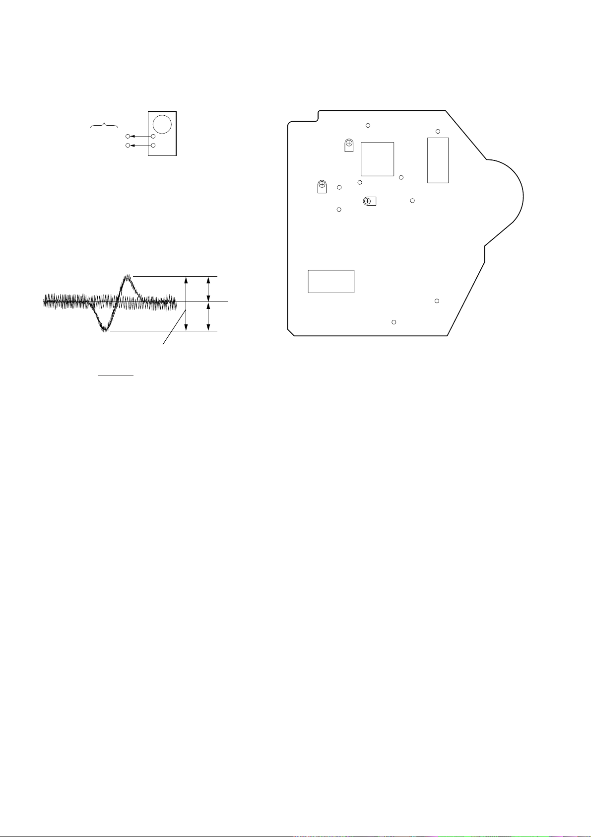
E-F Balance (1 Track Jump) Check
V
(Without remote commander)
oscilloscope
BD board
TP (TE)
TP (VC)
+
–
Procedure :
1. Connect oscilloscpe to test point TP (TE) on BD board.
2. Turn Power switch on.
3. Put disc (YEDS-18) in to play the number five track.
4. Press the “P (Pause)” button. (Becomes the 1 track jump mode)
5. Confirm that the oscilloscope waveform is symmetrical on the
top and bottom in relation to 0Vdc, and check this level.
1 track jump waveform
Adjustment Location:
[BD BOARD] — Component Side —
RF
RV101
IC101
RV103
TEO
VC
FEO
RV102
TEI
FEI
FOK
IC102
A
0
B
LEVEL : 300 ± 100 mVp-p
Specified level: • x 100 = less than ± 7%
A – B
2 (A + B)
• A + B = 300 ± 100 mVp-p
6. Remove the lead wire connected in step 1.
Focus/Tracking Gain Adjustment (RV102, RV103)
This gain has a margin, so even if it is slightly off.
There is no problem.
Therfore, do not perform this adjustment.
Please note that it should be fixed to mechanical center position
when you moved and do not know original position.
IC104
PCK
GND
– 12 –
Page 13
5-1. CIRCUIT BOARDS LOCATION
d
FM/AM TUNER
THIS BLOCK IS SUPPLIED
AS THE ASSEMBLED BLOCK
TAPE PREAMP board
SECTION 5
DIAGRAMS
FUN/SURROUND boar
VOL/POWER board
DISPLAY board
CONTROL BLK ASSY
THIS BLOCK IS SUPPLIED
AS THE ASSEMBLED BLOCK
BD board
CD DOOR SW board
RELAY board
– 13 –
Page 14

5-2. IC PIN FUNCTION
• IC201 MASTER CONTROL (TC9613)
Pin No. Pin Name I/O Function
1
2
3
4
5
6
7
8
9
10
11
12
13
14
15
16
17
18
19
20
21
22
23
24
25
26
27
28
29
30
31
32
33
34
35
36
37
38
39
40
41
42
43
44
45
46
47
48
49
50
GND
XOUT
XIN
RESET
TUNED
STEREO
TEST
POWDEC
REMOTE
PLL CE
PLL CLK
PLL DATAI
PLL DATAO
SERVO CK
SUB Q
DATA
MUTE D
CDPOWER
CLOSESW
FSW
SENSE
MLAT
XLAT
XRST
SCOR
PLAYSW
MTRSNS
TAPEIN
MOTOR
SOL
AMS
PLYMUTE
REC/PB
DOLBYNR
RECMUTE
BIAS
REC LED
CD SYNC
WIDE
KEYIO 1
KEYIO 2
BANDAREA
N.C
LOUDSEL
N.C
FRECSW
RRECSW
AREF
AGND
GND
—
Ground
O
8 MHz Oscillator output
I
8 MHz Oscillator input
I
CPU reset input
I
Station detector input
I
Stereo signal input
I
Test pin (Connected to ground)
I
Power down detect input
I
Remote signal input
O
Chip enable output
O
Clock output
I
Data input
O
Data output
O
Servo clock output
I
Servo subq data & status input
O
Servo command data output
O
Digital mute control output
O
CD power supply output
I
Top loading close switch input
O
Servo focus down output
I
Servo status SENSE input
O
D/A MLAT output
O
Servo command latch output
O
Servo chip reset output
I
Servo SUBQ sync input
I
Tape play switch input
I
Tape motor reel sense input
I
Tape in switch input
O
Tape control output
O
Tape control output
I
Tape music search input
O
Tape play back mute signal output
O
Tape control output
O
Tape control output
O
Tape recording mute signal output
O
Tape control output
O
Record LED output
O
CD SYNC LED output
O
Wide LED output
I
AD key input (16 keys)
I
AD key input (16 keys)
—
Band area option (Not used)
—
Not used
I
Loudness initial select input
—
Not used
I
Tape forward record switch input
I
Tape reverse record switch input
I
A/D convert refrence input (+5V)
I
A/D convert Input ground input
—
Ground
– 14 –
Page 15

Pin No. Pin Name I/O Function
51
52
53
54
55
56
57
58
59
60
61
62
63
64-91
92
93
94
95
96
97
98
99
100
VDD
NARROW
NORMAL
LOUD
DBFB
VOL CLK
VOL DATA
VOL STB
FUNC A
FUNC B
MDMUTE
POWER
MUTE A
SEG27-SEG0
COM3
COM2
COM1
COM0
VLC
N.C
N.C
N.C
VDD
—
+5V power supply
O
Narrow LED output
O
Normal LED output
O
Loudness on/off control output
—
Not used (Connected to ground)
O
Volume control clock output
O
Volume control data output
O
Volume control strobe output
O
TAPE/TUNER control signal output (00: TAPE/01: TUNER)
O
CD/MD control signal output (10: CD/11: MD)
O
MD/REC ON mute output
O
System power output
O
Audio mute control output
O
LCD segment output
O
LCD common 3 output
O
LCD common 2 output
O
LCD common 1 output
O
LCD common 0 output
O
LCD drive power supply output
—
Not used (Connected to ground)
—
Not used (Connected to ground)
—
Not used (Connected to ground)
—
+5V power supply
– 15 –
Page 16

Page 17

Page 18

Page 19

Page 20

Page 21

Page 22

Page 23

Page 24

Page 25

Page 26

5-13. IC BLOCK DIAGRAMS
1
2
3
4
5
6
7
8
9
10
11
12
13
14
15
16
17
18
51
50
49
48
47
46
45
44
43
42
41
40
39
38
37
36
35
34
33
32313029282726252423222120
52535455565758596061626364
19
FOK
MON
MDP
MDS
LOCK
TEST
FILO
FILI
PCO
VSS
AVSS
CLTV
AVDD
RF
BIAS
ASYI
ASYO
ASYE
WDCK
DATA
XRST
SENS
MUTE
SQCK
SQSO
EXCK
SBSO
SCOR
V
SS
WFCK
EMPH
DOUT
C4M
FSTT
XTSL
XTAO
XTAI
MNTO
SERVO AUTO
SEQUENCER
CPU
INTERFACE
DIGITAL
CLV
SUB CODE
PROCESSOR
EFM
DEMODULATOR
DIGITAL
PLL
ASYMMETRY
CORRECTOR
D/A
INTERFACE
ERROR
CORRECTOR
16K
RAM
DIGITAL
OUT
CLOCK
GENERATOR
LRCK
BCLK
GTOP
XUGF
XPCK
V
DD
GFS
RFCK
CZPO
XROF
MNT3
MNT1
XLON
SPOD
SPOC
SPOB
SPOA
CLKO
V
DD
XLTO
DATO
CNIN
SEIN
CLOK
XLAT
3
5
14
4
5
3
6
CD SECTION
IC102 BA6397FP
IC101 CXA1782BQ
BUFFER
PHD2
PHD1
36
35 34
37FE BIAS
38F
39E
40EI
41VEE
42TEO
43LPFI
44TEI
45ATSC
46TZC
47TDFCT
48VC
F IV AMP
BAL1
BAL2
TOG1
TOG2
• WINDOW COMP
PHD
–
+
–
+
APC
–
+
RF IV AMP1
+
RF IV AMP2
–
+
–
+
E IV AMP
BAL3
TOG3
ATSC
–
+
–
TE AMP
33
+
–
FE AMP
+
1
FEO
LD
–
2
FEI
–
+
32
DFCT
3
FDFCT
RF M
–
+
FOK
+
LEVELS
–
TTL
IIL
–
+
FZC COMP
TZC COMP
DFCT
FS4
RF O
31
–
+
–
+
• IIL DATA RESISTOR • INPUT SHIFT RESISTOR
RF I
30
–
+
+
–
MIRR
TOG1-3 FS1-4 TG1-2 TM1-7 PS1-4
BAL1-3
–
–
+
+
–
• ADDRESS DECODER
+
• OUTPUT DECODER
CB
29CP28
DFCT
CC126CC225FOK
27
OUT1A
–
+
24 SENS
IIL
+
–
TTL
TTL
23 C. OUT
22 XRST
21 DATA
20 XLT
IIL
19 CLK
18 VCC
OUT1B
IN1A
IN1B
TR-B
REG 0
XRST
GND
IN2A
IN2B
OUT2A
OUT2B
GND
OP-OUT
–
+
HPF COMP LPF COMP
–
+
+
–
TM1
4
FGD
• FCS PHASE
COMPENSATION
5
FLB
FS2
+
–
6
FE O
TG1
FS1
7
FE M
• TRACKING
• PHASE
COMPENSATION
9
8
TGU
SRCH
TM7
TG2
TM6
TM5
TM4
TM3
• ISET
TM2
• F SET
TG2
11
FSET
10
17 ISET
–
16 SL 0
+
15 SL M
14 SL P
+
1312TA O
–
TA M
DRIVE
1
2
BUFFER
DRIVE
3
4
5
6
7
8
9
BUFFER
10
11
12
13
14
DRIVE
BUFFER
DRIVE
LEVEL
SHIFT
LEVEL
SHIFT
IC103 CXD2507AQ
THERMAL
SHUT DOWN
REGULATOR
DRIVER MUTE
LEVEL
SHIFT
LEVEL
SHIFT
BUFFER
DRIVE
BUFFER
DRIVE
BUFFER
DRIVE
BUFFER
DRIVE
28
GND
27
OUT4A
26
OUT4B
25
IN4A
24
IN4B
23
VC
VCC VCC
22
CC
V
21
VCC
20
IN3B
19
IN3A
18
OUT3B
17
OUT3A
16
OP+
15
OP–
– 41 –
– 42 –
Page 27

IC104 PCM1710U-B
LRCIN
DIN
BCKIN
CLKO
XTI
XTO
DGND
V
VCC2R
GND2R
EXT1R
EXT2R
VOUTR
GND1
1
2
3
4
5
6
7
8
DD
9
10
11
12
13
14
INPUT
INTERFACE DIGITAL
TIMING
CONTROL
5-LEVEL DAC
RIGHT
LOW-PASS FILTER
RIGHT
3-STAGE AMP
RIGHT
FILTER
NOISE
SHAPER
MODE
CONTROL
5-LEVEL DAC
LEFT
LOW-PASS FILTER
LEFT
3-STAGE AMP
LEFT
28
27
26
25
24
23
22
21
20
19
18
17
16
15
ML/DSD
MC/DM2
MD/DM1
MUTE
MODE
CKSL
DGND
DD
V
VCC2L
GND2L
EXT1L
EXT2L
VOUTL
VCC1
DECK SECTION
IC701 BA3126N
1
2 3
GND
REC SW1
POWER SECTION
IC461 TC9260P
1VSS
2
OUT
3
IN
L-CH
VOLUME
LD1
LD2
4
5
PB SW1
4
CONT
INPUT/OUTPUT SECTION
IC301 MC14052BCP
VDD
2
1
141516 13 12 11 10 9
5
GND
L-CH
LATCH
6
7
VCC
PB SW2
R-CH
LATCH
9
8
GND
REC SW2
12 3 456 78
0
2
16
VDD
15
OUT
14
IN
LD1
LD2
R-CH
VOLUME
13
12
COMMON30
COMMON
SEL.A
SEL.B
DECODER
3
1
INHIBIT
EE
V
VSS
AGND
11
6
CS
7
8
CK
DATA DECODER,
STB GENERATOR
INPUT REGISTER
AGND
10
STB
9
DATA
– 43 –
Page 28

IC351 TA2041F
13
GND
VREF
14
OUT1
15
BIAS
12
CC
V
EXT IN
PS4
PS3
HF1
LF IN1
VCC
VCC
16
SWITCH
abc
VCC
17
LF5
18
19
VCC
20
LF4
21
LF3
VCC
22
23
IN1
24
VCC
VCC
SWITCH
V
CC
VCC
11
SW
c
a
b
VCC
VCC
VCC
VCC
SWB
10
SWA
9
OUT2
MIX
8
LEVEL
SW C
7
6
LF2
PS2
5
PS1
4
3
LF1
LF IN2
2
1
IN2
– 44 –
Page 29

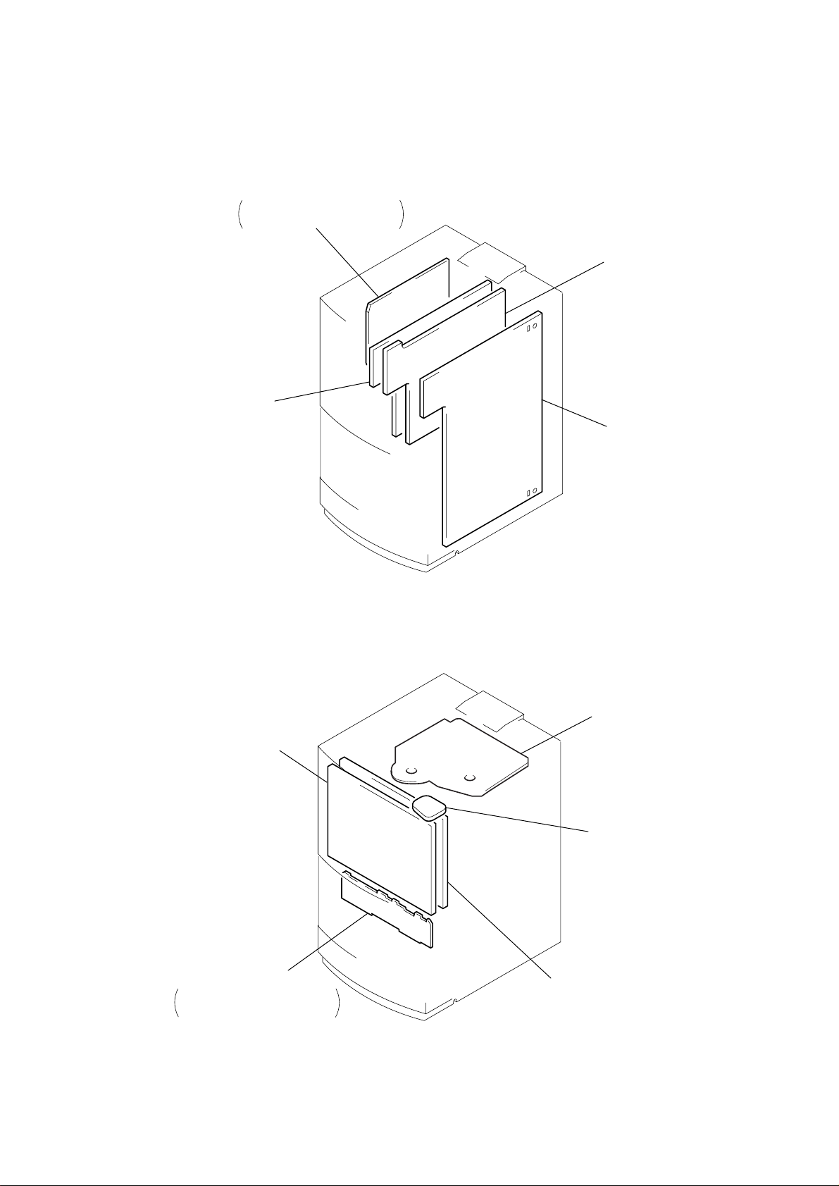
SECTION 6
t
EXPLODED VIEWS
NOTE:
• -XX, -X mean standardized parts, so they may have
some difference from the original one.
• Items marked “*” are not stocked since they are
seldom required for routine service. Some delay
should be anticipated when ordering these items.
• The mechanical parts with no reference number in
the exploded views are not supplied.
6-1. CD SECTION
18
#3
10
#2
9
• Hardware (# mark) list and accessories and packing materials are given in the last of this parts list.
• Abbreviation
CND : Canadian model
EE : East European model
HK : Hong Kong model
SP : Singapore model
MY : Malaysia model
2
4
5
7
8
17
#1
The components identified by
mark ! or dotted line with mark
! are critical for safety.
Replace only with part number
specified.
Les composants identifiés par une
marque ! sont critiques pour la
sécurité.
Ne les remplacer que par une
piéce portant le numéro spécifié.
1
3
6
4
#2
16
#4
#2
#3
14
#2
10
11
12
18
#3
13
#5
#5
15
#5
Base uni
11
12
#3
Ref. No. Part No. Description Remark Ref. No. Part No. Description Remark
1 4-997-375-01 GLASS DOOR W/PRINGING
2 4-997-373-01 HINGE PLATE
3 4-997-355-01 DOOR HINGE
4 4-997-365-01 HINGE PIN
5 4-997-370-01 BAR RUBBER
6 4-997-356-01 HINGE SPRING
7 4-997-349-01 CD BASE
8 4-997-367-01 PUSH BUTTON
9 4-997-369-01 CUSHION
10 4-997-345-01 HOOK SCREW
11 4-948-503-01 SPRING (BU), COMPRESSION
12 4-997-372-01 WASHER
13 1-783-091-11 WIRE (FLAT TYPE)
* 14 4-997-350-01 BACK COVER (US,CND,MY,SP,HK)
* 14 4-997-350-11 BACK COVER (AEP,UK,EE,CIS)
15 4-997-353-01 PICK UP COVER
* 16 A-4407-244-A CD DOOR SW BOARD, COMPLETE
17 4-977-376-01 STOP SPRING
18 4-977-371-01 STOPPER
– 45 –
Page 30

6-2. REAR PANEL SECTION
d
65
66
64
54
(UK)
54
(EXCEPT
US,CND,UK)
not supplied
51
#8
62
#7
56
#8
T501
57
52
62
58
#7
53
#7
62
#6
S501 (MY,
SP,HK)
62
#7
#7
#6
#13
#7
#6
#7
55
51
63
(HK)
54
(US,CND)
not supplie
59
FRONT PANEL
#7
61
Ref. No. Part No. Description Remark Ref. No. Part No. Description Remark
* 51 4-997-363-01 SIDE BRACKET
52 1-693-400-21 FM/AM TUNER (AEP,UK,EE,CIS)
52 1-693-400-31 FM/AM TUNER (US,CND)
52 1-693-400-41 FM/AM TUNER (MY,SP,HK)
* 53 4-997-368-11 REAR PANEL (AEP)
* 53 4-997-368-21 REAR PANEL (UK)
* 53 4-997-368-31 REAR PANEL (EE,CIS)
* 53 4-997-368-41 REAR PANEL (US,CND)
* 53 4-997-368-51 REAR PANEL (MY,SP)
* 53 4-997-368-61 REAR PANEL (HK)
! 54 1-551-478-00 CORD, POWER (POLAR.SPT-2)(US,CND)
! 54 1-555-750-00 CORD, POWER (AEP,EE,CIS,MY,SP,HK)
! 54 1-751-535-11 CORD, POWER (UK)
55 4-997-358-01 AC CORD BUSHING
* 56 A-4407-243-A TAPE PREAMP BOARD, COMPLETE
60
The components identified by
61
mark ! or dotted line with mark
! are critical for safety.
Replace only with part number
specified.
* 58 A-4407-239-A VOL/POWER BOARD, COMPLETE
* 58 A-4407-240-A VOL/POWER BOARD, COMPLETE (US,CND)
* 58 A-4407-241-A VOL/POWER BOARD, COMPLETE (MY,SP,HK)
* 59 4-997-364-01 BOTTOM BOARD
60 4-997-352-01 BOTTOM COVER
61 4-997-366-01 RUBBER FOOT
* 62 4-997-378-01 PC BOARD BRACKET
! 63 1-770-019-11 ADAPTOR, CONVERSION PLUG 3P (HK)
64 X-4949-451-1 AM ANT SUB ASSY
65 1-501-659-11 ANTENNA (FM) (US,CND,MY,SP,HK)
66 1-501-985-11 LEAD, ANTENNA (AEP,UK,EE,CIS)
! S501 1-771-308-11 SELECTOR, POWER (MY,SP,HK)
! T501 1-431-697-21 TRANSFORMER, POWER (AEP,UK,EE,CIS)
! T501 1-431-697-31 TRANSFORMER, POWER (US,CND)
Les composants identifiés par
une marque ! sont critiques pour
la sécurité.
Ne les remplacer que par une
piéce portant le numéro spécifié.
(AEP,UK,EE,CIS)
* 57 A-4407-242-A FUN/SURROUND BOARD, COMPLETE
! T501 1-431-697-41 TRANSFORMER, POWER (MY,SP,HK)
– 46 –
Page 31

6-3. FRONT PANEL SECTION
Z201
102
114
113
103
112
105
104
#7
106
#7
109
#6
107
111
#9
#6
110
#5
115
108
101
Ref. No. Part No. Description Remark Ref. No. Part No. Description Remark
101 4-997-351-01 DOOR COVER
102 4-997-354-01 DOOR SPRING
103 X-4949-450-1 CASS DOOR SUB ASSY
104 1-773-009-11 WIRE (FLAT TYPE) (15 CORE) (AEP,UK,EE,CIS)
104 1-751-688-11 WIRE (FLAT TYPE) (13 CORE)
(US,CND,MY,SP,HK)
* 105 A-4407-247-A DISPLAY BOARD, COMPLETE (AEP,UK,EE,CIS)
* 105 A-4407-248-A DISPLAY BOARD, COMPLETE (US,CND)
* 105 A-4407-249-A DISPLAY BOARD, COMPLETE (MY,SP,HK)
* 106 A-4407-245-A RELAY BOARD, COMPLETE
107 4-997-361-01 GEAR DAMPER
108 X-4949-449-1 FRONT PANEL SUB ASSY
109 4-997-362-01 DOOR LATCH
110 1-759-548-11 DECK, MECHANICAL
111 4-997-357-01 GEAR HOLDER
112 4-997-381-01 LCD HOLDER
113 4-997-382-01 LIGHT BAR
114 4-997-383-01 DISPLAY FILTER
115 4-997-374-01 SOLDER LUG
Z201 1-803-020-11 DISPLAY PANEL, LIQUID CRYSTAL
– 47 –
Page 32

Ver 1.1 2001.06
6-4. MECHANISM DECK SECTION (CASSETTE)
152
not supplied
not supplied
not supplied
not
not supplied
not supplied
not supplied
supplied
not supplied
M901
not supplied
not supplied
155
153
157
not supplied
not supplied
#11
#11
not
supplied
(including )
154
not supplied
A
A
not
supplied
#12
156
151
159
not
supplied
not supplied
not supplied
158
Ref. No. Part No. Description Remark
151 1-759-548-11 DECK, MECHANICAL
152 X-4949-565-1 CONTROL BLK ASSY
153 X-4949-566-1 CLUTCH BLK ASSY
154 X-4949-563-1 PLA TE HD BLK ASSY
155 4-997-983-01 BEL T MAIN
156 X-4949-568-1 ROLLER PINCH BLK R ASSY
157 X-4949-569-1 ROLLER PINCH BLK L ASSY
158 4-997-984-01 F/R BEL T
159 X-4949-567-1 CLUTCH BLK2 ASSY
M901 X-4949-564-1 MTR MAIN BLK ASSY (CAPST AN/REEL)
– 48 –
Page 33

6-5. BASE UNIT SECTION (BU17-BD19)
Ver 1.1 2001.06
201
202
#10
203
205
204
M101
M102
207
208
The components identified by
mark ! or dotted line with mark
! are critical for safety.
Replace only with part number
specified.
204
206
Les composants identifiés par
une marque ! sont critiques pour
la sécurité.
Ne les remplacer que par une
piéce portant le numéro spécifié.
Ref. No. Part No. Description Remark Ref. No. Part No. Description Remark
! 201 8-848-387-01 OPTICAL PICK-UP KSS-213BA/S-N
202 1-769-069-11 WIRE (FLAT TYPE) (16 CORE)
203 4-917-567-01 GEAR (M)
204 4-951-940-01 INSULATOR (BU)
205 4-917-565-01 SHAFT, SLED
206 4-917-564-01 GEAR (P), FLATNESS
* 207 A-4673-402-B BD BOARD, COMPLETE
208 4-951-620-01 SCREW (2.6X8), +BVTP
M101X-4950-066-1 MOTOR ASSY (SPINDLE)
M102 X-4917-504-1 MOTOR ASSY (SLED)
– 49 –
Page 34

BD
Note:
The components identified by
mark ! or dotted line with mark
! are critical for safety.
Replace only with part number
specified.
Les composants identifiés par une
marque ! sont critiques pour la
sécurité.
Ne les remplacer que par une
piéce portant le numéro spécifié.
When indicating parts by reference
number, please include the boar d
name.
Ref. No. Part No. Description Remark Ref. No. Part No. Description Remark
* A-4673-402-B BD BOARD, COMPLETE
******************
< CAPACITOR >
ELECTRICAL PARTS LIST
• Due to standardization, replacements in the parts list
may be different from the parts specified in the
diagrams or the components used on the set.
• -XX, -X mean standardized parts, so they may have
some difference from the original one.
• Items marked “*” are not stocked since they are
seldom required for routine service. Some delay
should be anticipated when ordering these items.
• RESISTORS
All resistors are in ohms
METAL: Metal-film resistor
METAL OXIDE: Metal Oxide-film resistor
F : nonflammable
C146 1-135-201-11 TANTALUM CHIP 10uF 20% 4V
C147 1-163-275-11 CERAMIC CHIP 0.001uF 5% 50V
C148 1-163-275-11 CERAMIC CHIP 0.001uF 5% 50V
C149 1-164-346-11 CERAMIC CHIP 1uF 16V
• SEMICONDUCTORS
In each case, u: µ, for example:
uA...: µA..., uPA...: µPA..., uPB...: µ PB ...,
uPC...: µPC..., uPD...: µ PD...
• CAPACITORS
uF : µF
• COILS
uH : µH
• Abbreviation
CND : Canadian model
EE : East European model
HK : Hong Kong model
SP : Singapore model
MY : Malaysia model
SECTION 7
C101 1-126-607-11 ELECT CHIP 47uF 20% 4V
C102 1-163-275-11 CERAMIC CHIP 0.001uF 5% 50V
C103 1-164-346-11 CERAMIC CHIP 1uF 16V
C105 1-163-038-91 CERAMIC CHIP 0.1uF 25V
C106 1-164-695-11 CERAMIC CHIP 0.0022uF 5% 50V
C107 1-164-695-11 CERAMIC CHIP 0.0022uF 5% 50V
C108 1-164-232-11 CERAMIC CHIP 0.01uF 50V
C109 1-164-232-11 CERAMIC CHIP 0.01uF 50V
C110 1-163-989-11 CERAMIC CHIP 0.033uF 10% 25V
C111 1-163-038-91 CERAMIC CHIP 0.1uF 25V
C112 1-163-038-91 CERAMIC CHIP 0.1uF 25V
C113 1-164-695-11 CERAMIC CHIP 0.0022uF 5% 50V
C114 1-164-005-11 CERAMIC CHIP 0.47uF 25V
C115 1-126-607-11 ELECT CHIP 47uF 20% 4V
C116 1-163-016-00 CERAMIC CHIP 0.0039uF 10% 50V
C117 1-164-005-11 CERAMIC CHIP 0.47uF 25V
C118 1-107-823-11 CERAMIC CHIP 0.47uF 10% 16V
C119 1-163-038-91 CERAMIC CHIP 0.1uF 25V
C120 1-135-201-11 TANTALUM CHIP 10uF 20% 4V
C121 1-163-038-91 CERAMIC CHIP 0.1uF 25V
C122 1-164-232-11 CERAMIC CHIP 0.01uF 50V
C123 1-163-038-91 CERAMIC CHIP 0.1uF 25V
C124 1-126-607-11 ELECT CHIP 47uF 20% 4V
C125 1-164-232-11 CERAMIC CHIP 0.01uF 50V
C126 1-163-038-91 CERAMIC CHIP 0.1uF 25V
C127 1-164-695-11 CERAMIC CHIP 0.0022uF 5% 50V
C128 1-163-135-00 CERAMIC CHIP 560PF 5% 50V
C129 1-163-038-91 CERAMIC CHIP 0.1uF 25V
C130 1-164-336-11 CERAMIC CHIP 0.33uF 25V
C131 1-163-038-91 CERAMIC CHIP 0.1uF 25V
C132 1-163-037-11 CERAMIC CHIP 0.022uF 10% 25V
C133 1-163-145-00 CERAMIC CHIP 0.0015uF 5% 50V
C134 1-164-346-11 CERAMIC CHIP 1uF 16V
C135 1-163-251-11 CERAMIC CHIP 100PF 5% 50V
C136 1-164-005-11 CERAMIC CHIP 0.47uF 25V
C137 1-164-232-11 CERAMIC CHIP 0.01uF 50V
C139 1-163-235-11 CERAMIC CHIP 22PF 5% 50V
C140 1-163-235-11 CERAMIC CHIP 22PF 5% 50V
C141 1-163-038-91 CERAMIC CHIP 0.1uF 25V
C142 1-163-038-91 CERAMIC CHIP 0.1uF 25V
C145 1-135-201-11 TANTALUM CHIP 10uF 20% 4V
C153 1-135-259-11 TANTAL. CHIP 10uF 20% 6.3V
C154 1-163-235-11 CERAMIC CHIP 22PF 5% 50V
< CONNECTOR >
CNU101 1-770-014-11 CONNECTOR, FFC/FPC 16P
CNU102 1-770-013-11 CONNECTOR, FFC/FPC 19P
< IC >
IC101 8-752-074-34 IC CXA1782CQ
IC102 8-759-291-06 IC BA6397FP
IC103 8-752-372-94 IC CXD2507AQ
IC104 8-759-185-29 IC PCM1710U-B
< MOTOR >
M101 X-4917-523-4 MOTOR ASSY (SPINDLE)
M102 X-4917-504-1 MOTOR ASSY (SLED)
< TRANSISTOR >
Q101 8-729-010-08 TRANSISTOR MSB710-R
Q102 8-729-424-08 TRANSISTOR UN2111
Q103 8-729-421-22 TRANSISTOR UN2211
< RESISTOR >
R102 1-216-001-00 METAL CHIP 10 5% 1/10W
R103 1-216-049-91 METAL GLAZE 1K 5% 1/10W
R104 1-216-097-91 METAL GLAZE 100K 5% 1/10W
R105 1-216-093-00 METAL CHIP 68K 5% 1/10W
R106 1-216-093-00 METAL CHIP 68K 5% 1/10W
R107 1-216-093-00 METAL CHIP 68K 5% 1/10W
R108 1-216-093-00 METAL CHIP 68K 5% 1/10W
R109 1-216-097-91 METAL GLAZE 100K 5% 1/10W
R112 1-216-083-00 METAL CHIP 27K 5% 1/10W
R113 1-216-083-00 METAL CHIP 27K 5% 1/10W
R114 1-216-101-00 METAL CHIP 150K 5% 1/10W
R115 1-216-101-00 METAL CHIP 150K 5% 1/10W
R116 1-216-061-00 METAL CHIP 3.3K 5% 1/10W
R117 1-216-069-00 METAL CHIP 6.8K 5% 1/10W
R118 1-216-049-91 METAL GLAZE 1K 5% 1/10W
R119 1-216-089-91 METAL GLAZE 47K 5% 1/10W
R120 1-216-089-91 METAL GLAZE 47K 5% 1/10W
R121 1-216-114-00 METAL GLAZE 510K 5% 1/10W
– 50 –
Page 35

DISPLAYCD DOOR SWBD
Ref. No. Part No. Description Remark Ref. No. Part No. Description Remark
R122 1-216-097-91 METAL GLAZE 100K 5% 1/10W
R123 1-216-099-00 METAL CHIP 120K 5% 1/10W
* A-4407-244-A CD DOOR SW BOARD, COMPLETE
***************************
R124 1-216-091-00 METAL CHIP 56K 5% 1/10W
R125 1-216-069-00 METAL CHIP 6.8K 5% 1/10W
R126 1-216-063-91 METAL GLAZE 3.9K 5% 1/10W
R127 1-216-089-91 METAL GLAZE 47K 5% 1/10W
R128 1-216-105-91 METAL GLAZE 220K 5% 1/10W
R129 1-216-049-91 METAL GLAZE 1K 5% 1/10W
R130 1-216-079-00 METAL CHIP 18K 5% 1/10W
R131 1-216-079-00 METAL CHIP 18K 5% 1/10W
R132 1-216-061-00 METAL CHIP 3.3K 5% 1/10W
R133 1-216-061-00 METAL CHIP 3.3K 5% 1/10W
R134 1-216-065-00 METAL CHIP 4.7K 5% 1/10W
R135 1-216-065-00 METAL CHIP 4.7K 5% 1/10W
R136 1-216-073-00 METAL CHIP 10K 5% 1/10W
R137 1-216-065-00 METAL CHIP 4.7K 5% 1/10W
R138 1-216-049-91 METAL GLAZE 1K 5% 1/10W
R139 1-216-033-00 METAL CHIP 220 5% 1/10W
R140 1-216-081-00 METAL CHIP 22K 5% 1/10W
R141 1-216-061-00 METAL CHIP 3.3K 5% 1/10W
R142 1-216-061-00 METAL CHIP 3.3K 5% 1/10W
R143 1-216-121-91 METAL GLAZE 1M 5% 1/10W
R144 1-216-073-00 METAL CHIP 10K 5% 1/10W
R145 1-216-097-91 METAL GLAZE 100K 5% 1/10W
R146 1-216-097-91 METAL GLAZE 100K 5% 1/10W
R147 1-216-049-91 METAL GLAZE 1K 5% 1/10W
R148 1-216-049-91 METAL GLAZE 1K 5% 1/10W
R149 1-216-049-91 METAL GLAZE 1K 5% 1/10W
R150 1-216-037-00 METAL CHIP 330 5% 1/10W
R151 1-216-037-00 METAL CHIP 330 5% 1/10W
R152 1-216-037-00 METAL CHIP 330 5% 1/10W
R153 1-216-082-00 METAL GLAZE 24K 5% 1/10W
R154 1-216-065-00 METAL CHIP 4.7K 5% 1/10W
R156 1-216-085-00 METAL CHIP 33K 5% 1/10W
R157 1-216-069-00 METAL CHIP 6.8K 5% 1/10W
R158 1-216-001-00 METAL CHIP 10 5% 1/10W
< SWITCH >
S211 1-771-298-11 SWITCH, PUSH (CD DOOR)
**************************************************************
* A-4407-247-A DISPLAY BOARD, COMPLETE (AEP,UK,EE,CIS)
*************************************
* A-4407-248-A DISPLAY BOARD, COMPLETE (US,CND)
*********************************
* A-4407-249-A DISPLAY BOARD, COMPLETE (MY,SP,HK)
***********************************
4-997-381-01 LCD HOLDER
4-997-382-01 LIGHT BAR
4-997-383-01 DISPLAY FILTER
< CAPACITOR >
C200 1-126-514-11 ELECT 22uF 20% 16V
C201 1-102-962-00 CERAMIC 30PF 5% 50V
C202 1-102-953-00 CERAMIC 18PF 5% 50V
C203 1-136-165-00 FILM 0.1uF 5% 50V
C204 1-136-165-00 FILM 0.1uF 5% 50V
C205 1-126-916-11 ELECT 1000uF 20% 6.3V
C206 1-136-165-00 FILM 0.1uF 5% 50V
C207 1-136-165-00 FILM 0.1uF 5% 50V
C208 1-136-165-00 FILM 0.1uF 5% 50V
C209 1-136-165-00 FILM 0.1uF 5% 50V
C212 1-136-165-00 FILM 0.1uF 5% 50V
C213 1-126-177-11 ELECT 100uF 20% 10V
C220 1-136-165-00 FILM 0.1uF 5% 50V
C230 1-102-934-00 CERAMIC 1.0PF +-0.25PF 50V
C232 1-126-177-11 ELECT 100uF 20% 10V
< CONNECTOR >
< VARIABLE RESISTOR >
RV101 1-241-396-11 RES, ADJ, METAL GLAZE 22K
RV102 1-241-396-11 RES, ADJ, METAL GLAZE 22K
RV103 1-241-396-11 RES, ADJ, METAL GLAZE 22K
< SWITCH >
S101 1-572-085-11 SWITCH, LEAF (LIMIT)
< VIBRATOR >
X101 1-579-280-11 VIBRATOR, CRYSTAL (16.9344MHz)
**************************************************************
* CN1 1-568-858-11 SOCKET, CONNECTOR 15P (AEP,UK,EE,CIS)
* CN1 1-784-568-11 CONNECTOR, FFC 13P (US,CND,SP,MY,HK)
< DIODE >
D201 8-719-920-76 DIODE 1S2076
D202 8-719-920-76 DIODE 1S2076
D203 8-719-920-76 DIODE 1S2076
D210 8-719-920-76 DIODE 1S2076
D211 8-719-920-76 DIODE 1S2076
D212 8-719-920-76 DIODE 1S2076
< IC >
IC201 8-759-497-90 IC TC9613
IC202 8-749-014-39 IC PIC-21041TH2
IC203 8-759-165-80 IC PST600C-T
< COIL >
L201 1-410-521-11 INDUCTOR 100uH
– 51 –
Page 36

DISPLAY FUN/SURROUND
Ref. No. Part No. Description Remark Ref. No. Part No. Description Remark
< DIODE >
LD201 8-719-989-30 DIODE EL204HD (WIDE)
LD202 8-719-989-30 DIODE EL204HD (NEAR F)
LD203 8-719-989-30 DIODE EL204HD (DBFB)
LD204 8-719-989-30 DIODE EL204HD (CD SYNC)
LD205 8-719-989-30 DIODE EL204HD (REC)
< CONNECTOR >
M201 1-784-348-11 CONNECTOR 12P
M202 1-784-347-11 CONNECTOR 10P
M203 1-784-349-11 CONNECTOR 25P
< LAMP >
R260 1-247-828-11 CARBON 750 5% 1/4W
R261 1-249-416-11 CARBON 820 5% 1/4W F
R262 1-249-418-11 CARBON 1.2K 5% 1/4W F
(US,CND)
R263 1-249-419-11 CARBON 1.5K 5% 1/4W F
R264 1-247-838-00 CARBON 2K 5% 1/4W
R270 1-249-393-11 CARBON 10 5% 1/4W F
R278 1-249-413-11 CARBON 470 5% 1/4W F
R279 1-249-413-11 CARBON 470 5% 1/4W F
R280 1-249-413-11 CARBON 470 5% 1/4W F
R281 1-249-413-11 CARBON 470 5% 1/4W F
R282 1-249-413-11 CARBON 470 5% 1/4W F
R290 1-249-429-11 CARBON 10K 5% 1/4W
PL201 1-517-743-11 LAMP
< TRANSISTOR >
Q201 8-729-119-78 TRANSISTOR 2SC2785-HFE
Q204 8-729-900-63 TRANSISTOR DTA124ES
Q205 8-729-900-63 TRANSISTOR DTA124ES
Q206 8-729-900-63 TRANSISTOR DTA124ES
Q207 8-729-900-63 TRANSISTOR DTA124ES
Q208 8-729-900-63 TRANSISTOR DTA124ES
< RESISTOR >
R200 1-249-429-11 CARBON 10K 5% 1/4W
R201 1-249-435-11 CARBON 33K 5% 1/4W
R202 1-249-424-11 CARBON 3.9K 5% 1/4W F
R203 1-249-429-11 CARBON 10K 5% 1/4W
R204 1-249-437-11 CARBON 47K 5% 1/4W
R205 1-249-429-11 CARBON 10K 5% 1/4W
R208 1-249-437-11 CARBON 47K 5% 1/4W
R209 1-249-429-11 CARBON 10K 5% 1/4W
R210 1-249-429-11 CARBON 10K 5% 1/4W
R222 1-249-429-11 CARBON 10K 5% 1/4W
R223 1-249-429-11 CARBON 10K 5% 1/4W
R225 1-249-429-11 CARBON 10K 5% 1/4W
R226 1-249-429-11 CARBON 10K 5% 1/4W
R227 1-249-429-11 CARBON 10K 5% 1/4W
R229 1-249-429-11 CARBON 10K 5% 1/4W
< SWITCH >
S200 1-571-760-11 SWITCH, KEY BOARD (POWER)
S201 1-571-760-11 SWITCH, KEY BOARD (VOLUME +)
S202 1-571-760-11 SWITCH, KEY BOARD (VOLUME –)
S203 1-571-760-11 SWITCH, KEY BOARD (TUNING +/) +)
S204 1-571-760-11 SWITCH, KEY BOARD (TUNING = 0/–)
S205 1-571-760-11 SWITCH, KEY BOARD (BAND P/FM)
S206 1-571-760-11 SWITCH, KEY BOARD (BAND AM/p)
S207 1-571-760-11 SWITCH, KEY BOARD (PLAY ª TC)
S208 1-571-760-11 SWITCH, KEY BOARD (PLAY CD/TC ·)
S209 1-571-760-11 SWITCH, KEY BOARD (FUNCTION)
S210 1-571-760-11 SWITCH, KEY BOARD (SOUND MODE)
< VIBRATOR >
X201 1-767-791-11 VIBRATOR, CRYSTAL (8MHz)
< LIQUID CRYSTAL DISPLAY >
Z201 1-803-020-11 DISPLAY PANEL, LIQUID CRYSTAL
**************************************************************
* A-4407-242-A FUN/SURROUND BOARD, COMPLETE
*****************************
* 4-997-378-01 PC BOARD BRACKET
7-685-646-79 SCREW +BVTP 3X8 TYPE2 N-S
R230 1-249-429-11 CARBON 10K 5% 1/4W
R239 1-249-425-11 CARBON 4.7K 5% 1/4W F
R240 1-249-425-11 CARBON 4.7K 5% 1/4W F
R246 1-249-429-11 CARBON 10K 5% 1/4W
R247 1-249-429-11 CARBON 10K 5% 1/4W
R248 1-249-429-11 CARBON 10K 5% 1/4W
R250 1-247-807-31 CARBON 100 5% 1/4W
R253 1-249-425-11 CARBON 4.7K 5% 1/4W F
(US,CND,AEP,UK,EE,CIS)
R254 1-249-420-11 CARBON 1.8K 5% 1/4W F
(US,CND)
R254 1-249-418-11 CARBON 1.2K 5% 1/4W F
(AEP,UK,EE,CIS)
R255 1-249-413-11 CARBON 470 5% 1/4W F
R256 1-249-412-11 CARBON 390 5% 1/4W F
R257 1-249-412-11 CARBON 390 5% 1/4W F
R258 1-249-414-11 CARBON 560 5% 1/4W F
R259 1-249-415-11 CARBON 680 5% 1/4W F
– 52 –
< CAPACITOR >
C307 1-102-074-00 CERAMIC 0.001uF 10% 50V
C308 1-102-074-00 CERAMIC 0.001uF 10% 50V
C309 1-124-907-11 ELECT 10uF 20% 50V
C310 1-126-963-11 ELECT 4.7uF 20% 50V
C311 1-161-772-11 CERAMIC 0.1uF 10% 25V
C312 1-161-772-11 CERAMIC 0.1uF 10% 25V
C313 1-126-963-11 ELECT 4.7uF 20% 50V
C314 1-126-963-11 ELECT 4.7uF 20% 50V
C315 1-124-907-11 ELECT 10uF 20% 50V
C316 1-124-907-11 ELECT 10uF 20% 50V
C317 1-124-443-00 ELECT 100uF 20% 10V
C318 1-124-443-00 ELECT 100uF 20% 10V
C319 1-102-114-00 CERAMIC 470PF 10% 50V
C320 1-102-114-00 CERAMIC 470PF 10% 50V
C351 1-137-378-11 FILM 0.22uF 5% 50V
C352 1-137-378-11 FILM 0.22uF 5% 50V
Page 37

FUN/SURROUND
Ref. No. Part No. Description Remark Ref. No. Part No. Description Remark
C353 1-137-378-11 FILM 0.22uF 5% 50V
C354 1-137-378-11 FILM 0.22uF 5% 50V
C355 1-137-371-11 FILM 0.015uF 5% 50V
C356 1-137-365-11 FILM 0.0015uF 5% 50V
R317 1-249-425-11 CARBON 4.7K 5% 1/4W F
R318 1-249-425-11 CARBON 4.7K 5% 1/4W F
R319 1-249-441-11 CARBON 100K 5% 1/4W
R320 1-249-441-11 CARBON 100K 5% 1/4W
RELAY
C357 1-130-489-00 MYLAR 0.033uF 5% 50V
C358 1-137-367-11 FILM 0.0033uF 5% 50V
C359 1-130-481-00 MYLAR 0.0068uF 5% 50V
C360 1-137-367-11 FILM 0.0033uF 5% 50V
C361 1-130-481-00 MYLAR 0.0068uF 5% 50V
C362 1-137-365-11 FILM 0.0015uF 5% 50V
C363 1-137-365-11 FILM 0.0015uF 5% 50V
C365 1-124-907-11 ELECT 10uF 20% 50V
C366 1-124-907-11 ELECT 10uF 20% 50V
C367 1-104-664-11 ELECT 47uF 20% 16V
C368 1-124-443-00 ELECT 100uF 20% 10V
C369 1-124-907-11 ELECT 10uF 20% 50V
C370 1-124-907-11 ELECT 10uF 20% 50V
C398 1-161-772-11 CERAMIC 0.1uF 10% 25V
< DIODE >
D351 8-719-920-76 DIODE 1S2076
D352 8-719-920-76 DIODE 1S2076
D353 8-719-920-76 DIODE 1S2076
< IC >
IC301 8-759-000-48 IC MC14052BCP
IC302 8-759-505-55 IC NJM4558L
IC351 8-759-497-89 IC TA-2041F
< JACK >
JK301 1-784-362-11 JACK, PIN 4P (MD IN/OUT)
< CONNECTOR >
M301 1-573-834-11 CONNECTOR, BOARD TO BOARD 20P
< TRANSISTOR >
Q301 8-729-231-55 TRANSISTOR 2SC2878-AB
Q302 8-729-231-55 TRANSISTOR 2SC2878-AB
Q303 8-729-201-53 TRANSISTOR 2SA1015-GR
< RESISTOR >
R301 1-249-417-11 CARBON 1K 5% 1/4W F
R302 1-249-417-11 CARBON 1K 5% 1/4W F
R303 1-249-417-11 CARBON 1K 5% 1/4W F
R304 1-249-417-11 CARBON 1K 5% 1/4W F
R305 1-249-417-11 CARBON 1K 5% 1/4W F
R306 1-249-417-11 CARBON 1K 5% 1/4W F
R307 1-249-425-11 CARBON 4.7K 5% 1/4W F
R308 1-249-425-11 CARBON 4.7K 5% 1/4W F
R309 1-249-421-11 CARBON 2.2K 5% 1/4W F
R310 1-249-421-11 CARBON 2.2K 5% 1/4W F
R311 1-249-441-11 CARBON 100K 5% 1/4W
R312 1-249-441-11 CARBON 100K 5% 1/4W
R313 1-249-441-11 CARBON 100K 5% 1/4W
R314 1-249-441-11 CARBON 100K 5% 1/4W
R315 1-249-441-11 CARBON 100K 5% 1/4W
R316 1-249-441-11 CARBON 100K 5% 1/4W
– 53 –
R321 1-247-903-00 CARBON 1M 5% 1/4W
R322 1-247-903-00 CARBON 1M 5% 1/4W
R323 1-249-417-11 CARBON 1K 5% 1/4W F
R324 1-249-417-11 CARBON 1K 5% 1/4W F
R329 1-247-815-91 CARBON 220 5% 1/4W
R330 1-247-815-91 CARBON 220 5% 1/4W
R335 1-249-425-11 CARBON 4.7K 5% 1/4W F
R336 1-249-425-11 CARBON 4.7K 5% 1/4W F
R337 1-249-417-11 CARBON 1K 5% 1/4W F
R338 1-249-417-11 CARBON 1K 5% 1/4W F
R339 1-249-441-11 CARBON 100K 5% 1/4W
R340 1-249-441-11 CARBON 100K 5% 1/4W
R341 1-249-437-11 CARBON 47K 5% 1/4W
R342 1-249-437-11 CARBON 47K 5% 1/4W
R343 1-249-425-11 CARBON 4.7K 5% 1/4W F
R344 1-249-425-11 CARBON 4.7K 5% 1/4W F
R345 1-249-437-11 CARBON 47K 5% 1/4W
R346 1-249-437-11 CARBON 47K 5% 1/4W
R347 1-249-425-11 CARBON 4.7K 5% 1/4W F
R348 1-249-421-11 CARBON 2.2K 5% 1/4W F
R351 1-249-430-11 CARBON 12K 5% 1/4W
R352 1-249-430-11 CARBON 12K 5% 1/4W
R353 1-249-431-11 CARBON 15K 5% 1/4W
R354 1-249-431-11 CARBON 15K 5% 1/4W
R355 1-249-429-11 CARBON 10K 5% 1/4W
R356 1-249-432-11 CARBON 18K 5% 1/4W
R357 1-249-425-11 CARBON 4.7K 5% 1/4W F
R358 1-249-425-11 CARBON 4.7K 5% 1/4W F
R359 1-249-437-11 CARBON 47K 5% 1/4W
R360 1-249-437-11 CARBON 47K 5% 1/4W
R361 1-249-417-11 CARBON 1K 5% 1/4W F
R362 1-249-417-11 CARBON 1K 5% 1/4W F
R363 1-249-429-11 CARBON 10K 5% 1/4W
R364 1-249-429-11 CARBON 10K 5% 1/4W
R367 1-249-417-11 CARBON 1K 5% 1/4W F
R368 1-249-417-11 CARBON 1K 5% 1/4W F
R369 1-249-421-11 CARBON 2.2K 5% 1/4W F
R370 1-249-421-11 CARBON 2.2K 5% 1/4W F
! R551 1-202-725-00 SOLID 3.3M 10% 1/2W
(US,CND)
**************************************************************
* A-4407-245-A RELAY BOARD, COMPLETE
**********************
< CAPACITOR >
C210 1-161-051-00 CERAMIC 0.01uF 10% 50V
C211 1-126-941-11 ELECT 470uF 20% 16V
C214 1-124-472-11 ELECT 470uF 20% 10V
C215 1-102-106-00 CERAMIC 100PF 10% 50V
C216 1-102-106-00 CERAMIC 100PF 10% 50V
C217 1-161-051-00 CERAMIC 0.01uF 10% 50V
C218 1-124-472-11 ELECT 470uF 20% 10V
The components identified by
mark ! or dotted line with mark
! are critical for safety.
Replace only with part number
specified.
Les composants identifiés par
une marque ! sont critiques pour
la sécurité.
Ne les remplacer que par une
piéce portant le numéro spécifié.
Page 38

RELAY
Ref. No. Part No. Description Remark Ref. No. Part No. Description Remark
C229 1-102-074-00 CERAMIC 0.001uF 10% 50V
C235 1-126-233-11 ELECT 22uF 20% 50V
C236 1-126-233-11 ELECT 22uF 20% 50V
C241 1-102-125-00 CERAMIC 4700PF 10% 50V
C242 1-102-125-00 CERAMIC 4700PF 10% 50V
C245 1-161-772-11 CERAMIC 0.1uF 10% 25V
C246 1-126-942-61 ELECT 1000uF 20% 16V
C789 1-161-051-00 CERAMIC 0.01uF 10% 50V
C797 1-161-051-00 CERAMIC 0.01uF 10% 50V
C799 1-161-051-00 CERAMIC 0.01uF 10% 50V
CNU102 1-770-067-11 CONNECTOR, FFC/FPC 19P
D200 8-719-911-55 DIODE U05G
D206 8-719-911-55 DIODE U05G
D207 8-719-911-55 DIODE U05G
D208 8-719-920-76 DIODE 1S2076
D209 8-719-920-76 DIODE 1S2076
D770 8-719-911-55 DIODE U05G
D771 8-719-911-55 DIODE U05G
TAPE PREAMP
< CONNECTOR >
< DIODE >
R235 1-249-429-11 CARBON 10K 5% 1/4W
R236 1-249-429-11 CARBON 10K 5% 1/4W
! R237 1-212-966-00 FUSIBLE 22 5% 1/2W F
R245 1-249-429-11 CARBON 10K 5% 1/4W
R265 1-249-429-11 CARBON 10K 5% 1/4W
R266 1-249-429-11 CARBON 10K 5% 1/4W
R267 1-249-429-11 CARBON 10K 5% 1/4W
R268 1-249-429-11 CARBON 10K 5% 1/4W
R271 1-249-429-11 CARBON 10K 5% 1/4W
R288 1-249-429-11 CARBON 10K 5% 1/4W
R289 1-249-429-11 CARBON 10K 5% 1/4W
R291 1-249-429-11 CARBON 10K 5% 1/4W
R295 1-249-415-11 CARBON 680 5% 1/4W F
R296 1-249-415-11 CARBON 680 5% 1/4W F
R298 1-249-435-11 CARBON 33K 5% 1/4W
R299 1-249-435-11 CARBON 33K 5% 1/4W
R771 1-249-425-11 CARBON 4.7K 5% 1/4W F
R772 1-249-434-11 CARBON 27K 5% 1/4W
R773 1-247-856-00 CARBON 11K 5% 1/4W
R774 1-249-430-11 CARBON 12K 5% 1/4W
R775 1-249-430-11 CARBON 12K 5% 1/4W
R776 1-249-418-11 CARBON 1.2K 5% 1/4W F
R777 1-249-418-11 CARBON 1.2K 5% 1/4W F
< COIL >
L203 1-408-096-00 INDUCTOR 470uH
< CONNECTOR >
* M704 1-564-715-11 PIN, CONNECTOR (SMALL TYPE)13P
< TRANSISTOR >
Q202 8-729-029-86 TRANSISTOR DTC124ESA
Q203 8-729-200-36 TRANSISTOR 2SA966-Y
Q213 8-729-029-86 TRANSISTOR DTC124ESA
Q214 8-729-029-86 TRANSISTOR DTC124ESA
Q215 8-729-029-86 TRANSISTOR DTC124ESA
Q770 8-729-200-36 TRANSISTOR 2SA966-Y
Q771 8-729-200-36 TRANSISTOR 2SA966-Y
Q772 8-729-029-86 TRANSISTOR DTC124ESA
Q773 8-729-029-86 TRANSISTOR DTC124ESA
< RESISTOR >
R206 1-249-430-11 CARBON 12K 5% 1/4W
R207 1-249-418-11 CARBON 1.2K 5% 1/4W F
R213 1-247-807-31 CARBON 100 5% 1/4W
R214 1-247-807-31 CARBON 100 5% 1/4W
R215 1-247-807-31 CARBON 100 5% 1/4W
R217 1-247-807-31 CARBON 100 5% 1/4W
R218 1-247-807-31 CARBON 100 5% 1/4W
R219 1-247-807-31 CARBON 100 5% 1/4W
R220 1-247-807-31 CARBON 100 5% 1/4W
R221 1-247-807-31 CARBON 100 5% 1/4W
R224 1-247-843-11 CARBON 3.3K 5% 1/4W
R231 1-249-429-11 CARBON 10K 5% 1/4W
R232 1-249-439-11 CARBON 68K 5% 1/4W
R233 1-249-429-11 CARBON 10K 5% 1/4W
R234 1-249-429-11 CARBON 10K 5% 1/4W
< VARIABLE RESISTOR >
VR770 1-230-497-11 RES, ADJ, CARBON 22K
< CONNECTOR >
* W103 1-564-704-11 PIN, CONNECTOR (SMALL TYPE) 2P
W201 1-784-351-11 CONNECTOR 12P
W202 1-784-350-11 CONNECTOR 10P
W203 1-784-352-11 CONNECTOR 25P
W301 1-573-852-11 CONNECTOR, BOARD TO BOARD 20P
W703 1-766-718-11 CONNECTOR, BOARD TO BOARD 17P
W901 1-766-718-11 CONNECTOR, BOARD TO BOARD 17P
**************************************************************
* A-4407-243-A TAPE PREAMP BOARD, COMPLETE
****************************
* 4-997-378-01 PC BOARD BRACKET
7-685-646-79 SCREW +BVTP 3X8 TYPE2 N-S
< CAPACITOR >
C483 1-161-051-00 CERAMIC 0.01uF 10% 50V
C484 1-161-051-00 CERAMIC 0.01uF 10% 50V
C700 1-161-051-00 CERAMIC 0.01uF 10% 50V
C703 1-102-113-00 CERAMIC 390PF 10% 50V
C704 1-102-113-00 CERAMIC 390PF 10% 50V
C705 1-104-666-11 ELECT 220uF 20% 10V
C706 1-104-666-11 ELECT 220uF 20% 10V
C707 1-102-106-00 CERAMIC 100PF 10% 50V
C708 1-102-106-00 CERAMIC 100PF 10% 50V
C709 1-137-372-11 FILM 0.022uF 5% 50V
C710 1-137-372-11 FILM 0.022uF 5% 50V
C711 1-124-907-11 ELECT 10uF 20% 50V
C712 1-124-907-11 ELECT 10uF 20% 50V
– 54 –
The components identified by
mark ! or dotted line with mark
! are critical for safety.
Replace only with part number
specified.
Les composants identifiés par
une marque ! sont critiques pour
la sécurité.
Ne les remplacer que par une
piéce portant le numéro spécifié.
Page 39

TAPE PREAMP
Ref. No. Part No. Description Remark Ref. No. Part No. Description Remark
C713 1-124-443-00 ELECT 100uF 20% 10V
C714 1-104-665-11 ELECT 100uF 20% 16V
C715 1-124-443-00 ELECT 100uF 20% 10V
C716 1-137-399-11 FILM 0.1uF 5% 50V
C717 1-124-907-11 ELECT 10uF 20% 50V
C719 1-161-051-00 CERAMIC 0.01uF 10% 50V
C720 1-161-051-00 CERAMIC 0.01uF 10% 50V
C721 1-102-981-00 CERAMIC 300PF 5% 50V
C722 1-102-981-00 CERAMIC 300PF 5% 50V
C723 1-102-112-00 CERAMIC 330PF 10% 50V
C724 1-102-112-00 CERAMIC 330PF 10% 50V
C725 1-102-112-00 CERAMIC 330PF 10% 50V
* M701 1-564-709-11 PIN, CONNECTOR (SMALL TYPE) 7P
* M703 1-766-720-21 CONNECTOR, BOARD TO BOARD 17P
Q702 8-729-194-57 TRANSISTOR 2SC945-P
Q704 8-729-194-57 TRANSISTOR 2SC945-P
Q705 8-729-194-57 TRANSISTOR 2SC945-P
Q706 8-729-141-83 TRANSISTOR 2SB1094-LK
Q707 8-729-194-57 TRANSISTOR 2SC945-P
< CONNECTOR >
< TRANSISTOR >
< RESISTOR >
C726 1-102-112-00 CERAMIC 330PF 10% 50V
C727 1-104-993-91 FILM 0.01uF 5% 200V
C728 1-124-907-11 ELECT 10uF 20% 50V
C729 1-137-371-11 FILM 0.015uF 5% 50V
C730 1-137-367-11 FILM 0.0033uF 5% 50V
C731 1-137-367-11 FILM 0.0033uF 5% 50V
C732 1-137-367-11 FILM 0.0033uF 5% 50V
C741 1-124-907-11 ELECT 10uF 20% 50V
C742 1-124-907-11 ELECT 10uF 20% 50V
C743 1-137-368-11 FILM 0.0047uF 5% 50V
C744 1-137-368-11 FILM 0.0047uF 5% 50V
C745 1-102-125-00 CERAMIC 4700PF 10% 50V
C746 1-102-125-00 CERAMIC 4700PF 10% 50V
C747 1-137-399-11 FILM 0.1uF 5% 50V
C748 1-137-399-11 FILM 0.1uF 5% 50V
C749 1-124-907-11 ELECT 10uF 20% 50V
C750 1-124-907-11 ELECT 10uF 20% 50V
C751 1-124-903-11 ELECT 1uF 20% 50V
C752 1-124-903-11 ELECT 1uF 20% 50V
C753 1-124-907-11 ELECT 10uF 20% 50V
C754 1-124-907-11 ELECT 10uF 20% 50V
C756 1-161-051-00 CERAMIC 0.01uF 10% 50V
C758 1-126-962-11 ELECT 3.3uF 20% 50V
C761 1-124-443-00 ELECT 100uF 20% 10V
C762 1-124-443-00 ELECT 100uF 20% 10V
R485 1-249-395-11 CARBON 15 5% 1/4W F
R486 1-249-395-11 CARBON 15 5% 1/4W F
R701 1-247-807-31 CARBON 100 5% 1/4W
R702 1-247-807-31 CARBON 100 5% 1/4W
R703 1-247-889-00 CARBON 270K 5% 1/4W
R704 1-247-889-00 CARBON 270K 5% 1/4W
R705 1-249-404-00 CARBON 82 5% 1/4W F
R706 1-249-404-00 CARBON 82 5% 1/4W F
R707 1-247-863-91 CARBON 22K 5% 1/4W
R708 1-247-863-91 CARBON 22K 5% 1/4W
R709 1-247-882-11 CARBON 130K 5% 1/4W
R710 1-247-882-11 CARBON 130K 5% 1/4W
R711 1-247-850-11 CARBON 6.2K 5% 1/4W
R712 1-247-850-11 CARBON 6.2K 5% 1/4W
R713 1-247-815-91 CARBON 220 5% 1/4W
R714 1-247-815-91 CARBON 220 5% 1/4W
R715 1-249-437-11 CARBON 47K 5% 1/4W
R716 1-247-815-91 CARBON 220 5% 1/4W
R717 1-249-430-11 CARBON 12K 5% 1/4W
R718 1-249-430-11 CARBON 12K 5% 1/4W
R719 1-249-389-11 CARBON 4.7 5% 1/4W F
R720 1-249-389-11 CARBON 4.7 5% 1/4W F
R721 1-247-863-91 CARBON 22K 5% 1/4W
R722 1-247-863-91 CARBON 22K 5% 1/4W
R723 1-249-381-11 CARBON 1 5% 1/4W F
C798 1-161-772-11 CERAMIC 0.1uF 10% 25V
C799 1-102-074-00 CERAMIC 0.001uF 10% 50V
C801 1-124-907-11 ELECT 10uF 20% 50V
C802 1-161-772-11 CERAMIC 0.1uF 10% 25V
< IC >
IC701 8-759-508-69 IC BA3126N
IC702 8-759-261-93 IC NJM4580LD
IC703 8-759-363-21 IC HA12203NT
JK800 8-749-923-04 IC TOTX178 (OPTICAL)
< JACK >
JK900 1-784-361-11 JACK (SMALL TYPE)(2)
< COIL >
L701 1-410-774-11 INDUCTOR 8.2mH
L702 1-410-774-11 INDUCTOR 8.2mH
L703 1-431-707-11 TRANSFORMER, BIAS OSCILLATION
L704 1-410-521-11 INDUCTOR 100uH
R724 1-247-863-91 CARBON 22K 5% 1/4W
R725 1-249-429-11 CARBON 10K 5% 1/4W
R741 1-249-435-11 CARBON 33K 5% 1/4W
R742 1-247-863-91 CARBON 22K 5% 1/4W
R743 1-249-417-11 CARBON 1K 5% 1/4W F
R744 1-249-417-11 CARBON 1K 5% 1/4W F
R745 1-249-426-11 CARBON 5.6K 5% 1/4W
R746 1-249-426-11 CARBON 5.6K 5% 1/4W
R749 1-249-441-11 CARBON 100K 5% 1/4W
R750 1-247-891-00 CARBON 330K 5% 1/4W
R751 1-249-429-11 CARBON 10K 5% 1/4W
R752 1-249-434-11 CARBON 27K 5% 1/4W
R753 1-249-429-11 CARBON 10K 5% 1/4W
R754 1-249-426-11 CARBON 5.6K 5% 1/4W
R757 1-249-429-11 CARBON 10K 5% 1/4W
R758 1-247-840-00 CARBON 2.4K 5% 1/4W
R759 1-249-432-11 CARBON 18K 5% 1/4W
R760 1-247-840-00 CARBON 2.4K 5% 1/4W
R761 1-247-866-11 CARBON 30K 5% 1/4W
R762 1-247-866-11 CARBON 30K 5% 1/4W
– 55 –
Page 40

Ver 1.1 2001.06
TAPE PREAMP VOL/POWER
Ref. No. Part No. Description Remark Ref. No. Part No. Description Remark
R763 1-249-437-11 CARBON 47K 5% 1/4W
R765 1-249-437-11 CARBON 47K 5% 1/4W
R766 1-249-437-11 CARBON 47K 5% 1/4W
< VARIABLE RESISTOR >
C510 1-126-943-11 ELECT 2200uF 20% 25V
C511 1-126-951-11 ELECT 470uF 20% 35V
C512 1-126-924-11 ELECT 330uF 20% 10V
C513 1-126-924-11 ELECT 330uF 20% 10V
C514 1-126-933-11 ELECT 100uF 20% 16V
VR701 1-230-499-11 RES, ADJ, CARBON 100K
VR702 1-230-499-11 RES, ADJ, CARBON 100K
VR703 1-230-497-11 RES, ADJ, CARBON 22K
VR704 1-230-497-11 RES, ADJ, CARBON 22K
VR705 1-230-495-11 RES, ADJ, CARBON 2K
VR706 1-230-495-11 RES, ADJ, CARBON 2K
**************************************************************
* A-4407-239-A VOL/POWER BOARD, COMPLETE
**************************
(AEP,UK,EE,CIS)
* A-4407-240-A VOL/POWER BOARD, COMPLETE (US,CND)
***********************************
* A-4407-241-A VOL/POWER BOARD, COMPLETE (MY,SP,HK)
*************************************
1-533-293-11 FUSE HOLDER
* 4-997-378-01 PC BOARD BRACKET
7-685-646-79 SCREW +BVTP 3X8 TYPE2 N-S
7-685-647-79 SCREW +BVTP 3X10 TYPE2 N-S
< CAPACITOR >
C403 1-136-173-00 FILM 0.47uF 5% 50V
C404 1-136-173-00 FILM 0.47uF 5% 50V
C461 1-126-960-11 ELECT 1uF 20% 50V
C462 1-126-960-11 ELECT 1uF 20% 50V
C463 1-137-364-11 FILM 0.001uF 5% 50V
C464 1-137-364-11 FILM 0.001uF 5% 50V
C465 1-137-378-11 FILM 0.22uF 5% 50V
C466 1-137-378-11 FILM 0.22uF 5% 50V
C469 1-126-933-11 ELECT 100uF 20% 16V
C470 1-126-925-11 ELECT 470uF 20% 10V
C515 1-126-933-11 ELECT 100uF 20% 16V
C516 1-162-851-11 CERAMIC 0.1uF 10% 16V
C517 1-162-851-11 CERAMIC 0.1uF 10% 16V
C518 1-162-851-11 CERAMIC 0.1uF 10% 16V
C519 1-126-923-11 ELECT 220uF 20% 10V
C520 1-126-923-11 ELECT 220uF 20% 10V
C521 1-162-851-11 CERAMIC 0.1uF 10% 16V
C522 1-126-924-11 ELECT 330uF 20% 10V
C523 1-126-924-11 ELECT 330uF 20% 10V
C525 1-126-924-11 ELECT 330uF 20% 10V
C526 1-126-924-11 ELECT 330uF 20% 10V
C527 1-162-851-11 CERAMIC 0.1uF 10% 16V
C528 1-126-924-11 ELECT 330uF 20% 10V
C529 1-126-933-11 ELECT 100uF 20% 16V
C530 1-162-851-11 CERAMIC 0.1uF 10% 16V
C531 1-162-851-11 CERAMIC 0.1uF 10% 16V
C532 1-126-933-11 ELECT 100uF 20% 16V
C999 1-161-772-11 CERAMIC 0.1uF 10% 25V
< DIODE >
D401 8-719-920-76 DIODE 1S2076
D402 8-719-920-76 DIODE 1S2076
D487 8-719-200-02 DIODE 10E2
D502 8-719-067-67 DIODE W02G
D503 8-719-001-64 DIODE UZL-12L2
D504 8-719-910-25 DIODE HZ12B2L
D506 8-719-001-85 DIODE UZL-12H3
D507 8-719-001-76 DIODE UZL-12M3
D508 8-719-001-42 DIODE UZL-11M1
D5098-719-935-81DIODE UZL-7L2
D510 8-719-200-02 DIODE 10E2
D511 8-719-920-76 DIODE 1S2076
C471 1-162-851-11 CERAMIC 0.1uF 10% 16V
C475 1-126-964-11 ELECT 10uF 20% 50V
C476 1-126-964-11 ELECT 10uF 20% 50V
C477 1-137-399-11 FILM 0.1uF 5% 50V
C478 1-137-399-11 FILM 0.1uF 5% 50V
C479 1-126-948-11 ELECT 100uF 20% 35V
C480 1-126-948-11 ELECT 100uF 20% 35V
C481 1-102-106-00 CERAMIC 100PF 10% 50V
C482 1-102-106-00 CERAMIC 100PF 10% 50V
C483A 1-124-443-00 ELECT 100uF 20% 10V
C485 1-102-106-00 CERAMIC 100PF 10% 50V
C486 1-102-106-00 CERAMIC 100PF 10% 50V
C488 1-126-924-11 ELECT 330uF 20% 10V
C489 1-161-063-00 CERAMIC 0.1uF 10% 50V
C490 1-126-963-11 ELECT 4.7uF 20% 50V
C491 1-126-963-11 ELECT 4.7uF 20% 50V
C502 1-102-129-00 CERAMIC 0.01uF 10% 50V
C503 1-102-129-00 CERAMIC 0.01uF 10% 50V
C508 1-126-964-11 ELECT 10uF 20% 50V
C509 1-126-947-11 ELECT 47uF 20% 35V
< FUSE >
! F501 1-532-350-11 FUSE, TIME-LAG (T4AL 250V)
(AEP,UK,EE,CIS,MY,SP,HK)
! F501 1-532-746-11 FUSE, GLASS TUBE (4A 125V)(US,CND)
! F502 1-532-259-11 FUSE, TIME-LAG (T1.6AL 250V)
(AEP,UK,EE,CIS,MY,SP,HK)
! F502 1-532-742-11 FUSE, GLASS TUBE (1.6A 125V)(US,CND)
! F503 1-532-259-11 FUSE, TIME-LAG (T1.6AL 250V)
(AEP,UK,EE,CIS,MY,SP,HK)
! F503 1-532-742-11 FUSE, GLASS TUBE (1.6A 125V)(US,CND)
! F504 1-532-350-11 FUSE, TIME-LAG (T4AL 250V)
(AEP,UK,EE,CIS,MY,SP,HK)
! F504 1-532-746-11 FUSE, GLASS TUBE (4A 125V)(US,CND)
< IC >
IC461 8-759-497-88 IC TC9260P
IC472 8-759-261-93 IC NJM4580LD
IC501 8-759-701-57 IC NJM78M06FA
The components identified by
mark ! or dotted line with mark
! are critical for safety.
Replace only with part number
specified.
Les composants identifiés par
une marque ! sont critiques pour
la sécurité.
Ne les remplacer que par une
piéce portant le numéro spécifié.
– 56 –
Page 41

VOL/POWER
Ref. No. Part No. Description Remark Ref. No. Part No. Description Remark
< JACK >
JK901 1-784-353-11 JACK (DIN)(SPEAKER L)
JK902 1-784-353-11 JACK (DIN)(SPEAKER R)
< CONNECTOR >
M501 1-564-234-11 PLUG, CONNECTOR (PIN CONTACT)8P
* M901 1-766-720-21 CONNECTOR, BOARD TO BOARD 17P
M902 1-564-707-11 PIN, CONNECTOR (SMALL TYPE) 5P
< TRANSISTOR >
Q486 8-729-201-53 TRANSISTOR 2SA1015-GR
Q487 8-729-231-55 TRANSISTOR 2SC2878-AB
Q488 8-729-231-55 TRANSISTOR 2SC2878-AB
Q501 8-729-281-53 TRANSISTOR 2SC1815-GR
Q502 8-729-201-53 TRANSISTOR 2SA1015-GR
Q503 8-729-201-53 TRANSISTOR 2SA1015-GR
Q504 8-729-209-15 TRANSISTOR 2SD2012
Q505 4-997-377-01 ISOLATION FILM
Q505 8-729-017-51 TRANSISTOR 2SB632K-E
Q506 8-729-281-53 TRANSISTOR 2SC1815-GR
Q507 4-997-377-01 ISOLATION FILM
Q507 8-729-188-23 TRANSISTOR 2SD882-P
Q508 4-997-377-01 ISOLATION FILM
Q508 8-729-188-23 TRANSISTOR 2SD882-P
Q509 4-997-377-01 ISOLATION FILM
Q509 8-729-188-23 TRANSISTOR 2SD882-P
Q510 8-729-017-51 TRANSISTOR 2SB632K-E
Q511 8-729-201-53 TRANSISTOR 2SA1015-GR
Q512 8-729-265-52 TRANSISTOR 2SC2655
R492 1-247-843-11 CARBON 3.3K 5% 1/4W
R493 1-249-437-11 CARBON 47K 5% 1/4W
R494 1-249-437-11 CARBON 47K 5% 1/4W
R495 1-249-425-11 CARBON 4.7K 5% 1/4W F
R496 1-249-425-11 CARBON 4.7K 5% 1/4W F
R497 1-249-441-11 CARBON 100K 5% 1/4W
R498 1-249-441-11 CARBON 100K 5% 1/4W
R499 1-247-895-91 CARBON 470K 5% 1/4W
! R501 1-213-044-51 FUSIBLE 2.2 5% 1W F
! R502 1-212-946-11 FUSIBLE 3.3 5% 1/2W F
R503 1-249-429-11 CARBON 10K 5% 1/4W
R504 1-249-421-11 CARBON 2.2K 5% 1/4W F
R505 1-247-863-91 CARBON 22K 5% 1/4W
R506 1-249-429-11 CARBON 10K 5% 1/4W
R507 1-249-437-11 CARBON 47K 5% 1/4W
R508 1-249-437-11 CARBON 47K 5% 1/4W
R509 1-247-807-31 CARBON 100 5% 1/4W
! R510 1-215-869-11 METAL OXIDE 1K 5% 1W F
R511 1-247-863-91 CARBON 22K 5% 1/4W
R512 1-249-431-11 CARBON 15K 5% 1/4W
! R514 1-212-853-00 FUSIBLE 6.8 5% 1/4W F
! R515 1-213-048-00 FUSIBLE 3.3 5% 1W F
R516 1-249-413-11 CARBON 470 5% 1/4W F
! R517 1-213-064-51 FUSIBLE 15 5% 1W F
R518 1-249-413-11 CARBON 470 5% 1/4W F
! R519 1-212-946-11 FUSIBLE 3.3 5% 1/2W F
R520 1-249-413-11 CARBON 470 5% 1/4W F
R521 1-249-413-11 CARBON 470 5% 1/4W F
R524 1-249-381-11 CARBON 1 5% 1/4W F
R525 1-247-887-00 CARBON 220K 5% 1/4W
< RESISTOR >
R457 1-247-863-91 CARBON 22K 5% 1/4W
R458 1-247-863-91 CARBON 22K 5% 1/4W
R461 1-249-429-11 CARBON 10K 5% 1/4W
R462 1-249-429-11 CARBON 10K 5% 1/4W
R463 1-247-895-91 CARBON 470K 5% 1/4W
R464 1-247-895-91 CARBON 470K 5% 1/4W
R465 1-249-425-11 CARBON 4.7K 5% 1/4W F
R466 1-247-815-91 CARBON 220 5% 1/4W
R467 1-249-429-11 CARBON 10K 5% 1/4W
R468 1-249-429-11 CARBON 10K 5% 1/4W
R469 1-249-429-11 CARBON 10K 5% 1/4W
R470 1-249-425-11 CARBON 4.7K 5% 1/4W F
R471 1-249-417-11 CARBON 1K 5% 1/4W F
R472 1-249-417-11 CARBON 1K 5% 1/4W F
R477 1-249-441-11 CARBON 100K 5% 1/4W
R478 1-249-441-11 CARBON 100K 5% 1/4W
R479 1-249-426-11 CARBON 5.6K 5% 1/4W
R480 1-249-426-11 CARBON 5.6K 5% 1/4W
R481 1-249-430-11 CARBON 12K 5% 1/4W
R482 1-249-430-11 CARBON 12K 5% 1/4W
R483 1-249-417-11 CARBON 1K 5% 1/4W F
R484 1-249-417-11 CARBON 1K 5% 1/4W F
R485A 1-249-429-11 CARBON 10K 5% 1/4W
R486A 1-249-429-11 CARBON 10K 5% 1/4W
R491 1-247-843-11 CARBON 3.3K 5% 1/4W
R526 1-249-441-11 CARBON 100K 5% 1/4W
R527 1-249-441-11 CARBON 100K 5% 1/4W
R528 1-249-425-11 CARBON 4.7K 5% 1/4W F
R529 1-249-437-11 CARBON 47K 5% 1/4W
< RELAY >
RL501 1-755-242-11 RELAY
**************************************************************
MISCELLANEOUS
*************
13 1-783-091-11 WIRE (FLAT TYPE)
52 1-693-400-21 FM/AM TUNER (AEP,UK,EE,CIS)
52 1-693-400-31 FM/AM TUNER (US,CND)
52 1-693-400-41 FM/AM TUNER (MY,SP,HK)
! 54 1-551-478-00 CORD, POWER (POLAR.SPT-2)(US,CND)
! 54 1-555-750-00 CORD, POWER (AEP,EE,CIS,MY,SP,HK)
! 54 1-751-535-11 CORD, POWER (UK)
! 63 1-770-019-11 ADAPTOR, CONVERSION PLUG 3P (HK)
65 1-501-659-11 ANTTENA (FM) (US,CND,MY,SP,HK)
66 1-501-985-11 LEAD, ANTTENA (AEP,UK,EE,CIS)
104 1-773-009-11 WIRE (FLAT TYPE) (15 CORE) (AEP,UK,EE,CIS)
104 1-751-688-11 WIRE (FLAT TYPE) (13 CORE)
(US,CND,MY,SP,HK)
110 1-759-548-11 DECK, MECHANICAL
151 1-759-548-11 DECK, MECHANICAL
! 201 8-848-387-01 OPTICAL PICK-UP KSS-213BA/S-N
– 57 –
The components identified by
mark ! or dotted line with mark
! are critical for safety.
Replace only with part number
specified.
Les composants identifiés par
une marque ! sont critiques pour
la sécurité.
Ne les remplacer que par une
piéce portant le numéro spécifié.
Page 42

HCD-ED1
Ref. No. Part No. Description Remark
202 1-769-069-11 WIRE (FLAT TYPE) (16 CORE)
M101 X-4917-523-4 MOTOR ASSY (SPINDLE)
M102 X-4917-504-1 MOTOR ASSY (SLED)
M901 X-4949-564-1 MTR MAIN BLK ASSY (CAPSTAN/REEL)
! S501 1-771-308-11 SELECTOR, POWER (MY,SP,HK)
! T501 1-431-697-21 TRANSFORMER, POWER (AEP,UK,EE,CIS)
! T501 1-431-697-31 TRANSFORMER, POWER (US,CND)
! T501 1-431-697-41 TRANSFORMER, POWER (MY,SP,HK)
Z201 1-803-020-11 DISPLAY PANEL, LIQUID CRYSTAL
**************************************************************
*************
HARDWARE LIST
*************
* #1 7-683-254-08 SET-SCT, HEX. 5X5 FLAT POINT
#2 7-682-248-09 SCREW +K 3X8
#3 7-685-105-19 TPG +P 2X8, TYPE 2, NON-SLIT
#4 7-685-134-19 SCREW +BTP 2.6X8 TYPE2 N-S
#5 7-685-131-19 SCREW +BTP 2.6X4 TYPE2 N-S
#6 7-685-647-79 SCREW +BVTP 3X10 TYPE2 N-S
#7 7-685-646-79 SCREW +BVTP 3X8 TYPE2 N-S
#8 7-685-880-09 SCREW +BVTT 4X6 (S)
* #9 7-627-000-02 SCREW,PRECISION+P M1.7X10 TYPE1
#10 7-621-255-15 SCREW +P 2X3
#11 7-627-553-88 SCREW,PRECISION+P 2X7
#12 7-627-554-28 SCREW,PRECISION+P M2X5 TYPE1
#13 7-682-546-09 SCREW +B 3X5
– 58 –
The components identified by
mark ! or dotted line with mark
! are critical for safety.
Replace only with part number
specified.
Les composants identifiés par
une marque ! sont critiques pour
la sécurité.
Ne les remplacer que par une
piéce portant le numéro spécifié.
Page 43

SERVICE MANUAL
HCD-ED1
US Model
Canadian Model
AEP Model
UK Model
1998. 04
SUPPLEMENT-1
File this supplement with the service manual.
• CHANGES OF LAMP
• The lamp on the DISPLAY board was changed to a type which use LED from following
serial numbers.
MODEL : Serial numbers
US, CND Model : 8107801 onward
AEP Model : 5155844 onward
UK Model : 6107951 onward
EE, CIS Model : 7104797 onward
MY, SP Model : 3153682 onward
HK Model : 3105301 onward
DIFFERENCE T ABLE
: Indicates changed portion.
Page
Ref. No. Part No. Description Remark
FORMER TYPE (use lamp)
*** EXPLODED VIEWS ***
E Model
(ENG-98003)
: 4107801 onward
NEW TYPE (use LED)
Ref. No. Part No. Description Remark
*** EXPLODED VIEWS ***
• Abbreviation
CND : Canadian model
EE : East European model
MY : Malaysia model
SP : Singapore model
HK : Hong Kong model
(SP)
47
52
PL201 1-517-743-11 LAMP
113
114
Z201
*** ELECTRICAL PARTS LIST ***
*** DISPLAY BOARD ***
105
112
104
Sony Corporation
Home A&V Products Company9-922-706-81
– 1 –
*116 1-670-517-11 LED BOARD
106
#7
#7
116
*** ELECTRICAL PARTS LIST ***
*** DISPLAY BOARD ***
98D091686-1
Printed in Japan © 1998. 4
Published by General Engineering Dept.
(Shibaura)
Page 44

FORMER TYPE (use lamp)Page
Ref. No. Part No. Description Remark
*** LED BOARD ***
NEW TYPE (use LED)
Ref. No. Part No. Description Remark
*** LED BOARD ***
–
SCHEMATIC DIAGRAM -DISPLAY SECTION- Page 31
Location: D-E, 9-10
* 1-670-517-11 LED BOARD
D1 8-719-064-63 DIODE SELU5823A-TP15
D2 8-719-064-63 DIODE SELU5823A-TP15
R1 1-247-807-11 CARBON 100 5% 1/4W
R2 1-249-404-00 CARBON 82 5% 1/4W
PRINTED WIRING BOARD -DISPLAY SECTION- Page 33
Location: C-E, 1-3
Note: Pattern of the rear side is not mentioned.
– 2 –
Page 45

MEMO
HCD-ED1
– 3 –
Page 46

HCD-ED1
REVISION HISTORY
Clicking the version allows you to jump to the revised page.
Also, clicking the version at the upper right on the revised page allows you to jump to the next revised
page.
Ver. Date Description of Revision
1.1
PDF registration. (including : 9-922-706-91)
1998.04 SUPPLEMENT-1
1.0
2001.06 Correction of clectrical parts list (D509). (SFD-01007)
1997.06 New
 Loading...