

Sony HCD-101 Service manual
HCD-101
SERVICE MANUAL
• HCD-101 is the CD PLAYER,
TUNER and AMPLIFIER
sections in CMT-101.
SPECIFICATIONS
AEP Model
UK Model
E Model
Tourist Model
Model Name Using Similar Mechanism NEW
CD Mechanism Type CDM50
Optical Pick-Up Type KSS-313A
Tuner section
T uning range
2 band model
European model: FM : 87.5-108MHz
(50kHz step)
AM : 522–1,611kHz
Other models: FM : 87.5–108MHz
(50kHz step)
AM : 531–1,602kHz
(at 9kHz interval)
530–1,710kHz
(at 10kHz interval)
3 band model FM : 87.5–108MHz
(50kHz step)
MW : 522–1,611kHz
(at 9kHz interval)
LW : 144–288kHz
(at 3kHz interval)
Intermediate frequency FM : 10.7MHz
AM : 450kHz
Aerial terminals FM : 75Ω unbalanced
AM : External aerial
terminal
Timer Quartz lock system
Timer setting One-minute step
Sleep timer 10–minute step, max.
90minutes
CD player section
System Compact disc digital
audio system
Laser Semiconductor laser
(λ=780nm)
Laser output power Less than 44.6µW*
* This output is the value measured at a distance of 200mm from
the objective lens surface on the optical pick-up block with 7mm
aperture.
Frequency response 5Hz–20kHz
Signal to noise ratio More than 90dB
Harmonic distortion Less than 0.05%
Amplifier section
European model:
DIN power output 15+15 W (4Ω at 1kHz, DIN
Continuous RMS power output
21+21 W (4Ω at 1kHz, 10%
THD)
Music power output 26+26 W
Other model
Rated RMS power output16+16 W (4Ω at 1kHz, 1% THD,
AC240V/AC120V)
Reference RMS power output
22+22 W (4Ω at 1kHz, 10% THD,
AC240V/AC120V)
Inputs VIDEO/PC IN jack : Stereo
phone jack, sensitivity 500mV,
impedance 47kΩ
— Continued on next page —
COMPACT COMPONENT SYSTEM
MICROFILM

TABLE OF CONTENTS
Outputs VIDEO/PC OUT jack : Stereo phone
jack, 250mV, 1kΩ
DIGIT AL OUT (CD OPTICAL OUT):
Square optical connector jack, –18dBm,
wave jength 660nm
PHONES (headphones) jack :
Stereo mini jack, accepts head phones of
8Ω or more.
General
Power requirements
European model 220–230V AC, 50/60Hz
Other models 110–120V or 220–240V
AC, 50/60Hz adjustable
with voltage selector
Power consumption 66W (when connected to TC-TX101,
MDS-MX101)
Dimensions Approx. 142×125×260mm (w/h/d) incl.
projecting parts and controls
Mass Approx. 4.1kg
SERVICE NOTE
NOTES ON HANDLING THE OPTICAL PICK-UP
BLOCK OR BASE UNIT
The laser diode in the optical pick-up block may suffer electrostatic
break-down because of the potential difference generated by the
charged electrostatic load, etc. on clothing and the human body.
During repair, pay attention to electrostatic break-down and also
use the procedure in the printed matter which is included in the
repair parts.
The flexible board is easily damaged and should be handled with
care.
1. GENERAL
······································································ 3
2. DISASSEMBLY
2-1. Case ····················································································4
2-2. Front Panel Section ···························································· 4
2-3. PRE Board ·········································································· 5
2-4. Function board, Relay board, SP TM board, Trans board,
Power board········································································ 5
2-5. Mechanism Deck ································································ 6
2-6. Chassis (T2) Assy······························································· 6
2-7. BD Board············································································ 7
2-8. Roller Arm Block Assy······················································· 7
2-9. Chassis (OPT), Chucking Arm Assy ·································· 8
2-10. Motor (SL) Assy (M102), Optical Pick-Up························ 8
3. TEST MODE ·································································· 9
4. ELECTRICAL ADJUSTMENT ······························ 11
5. DIAGRAMS
5-1. Circuit Boards Location ··················································· 14
5-2. Block Diagram ································································· 15
5-3. Schematic Diagram –BD Section– ··································· 18
5-4. Printed Wiring Board –BD Section–································ 21
5-5. Printed Wiring Board –Panel Section–····························· 23
5-6. Schematic Diagram –Panel Section – ······························ 25
5-7. Printed Wiring Board –PRE Section– ······························ 27
5-8. Schematic Diagram –PRE Section– ································· 29
5-9. Printed Wiring Board –Function Section– ······················· 31
5-10. Schematic Diagram –Function Section– ··························33
5-11. Printed Wiring Board –Power Section– ···························36
5-12. Schematic Diagram –Power Section– ······························39
5-13. IC Pin Function ································································ 42
5-14. IC Block Diagrams ··························································· 44
6. EXPLODED VIEWS
6-1. Front Panel Section ·························································· 47
6-2. Chassis Section································································· 48
6-3. Mechanism Deck Section-1 (CDM50)····························· 49
6-4. Mechanism Deck Section-2 (CDM50)····························· 50
7. ELECTRICAL PARTS LIST ···································51
NOTES ON LASER DIODE EMISSION CHECK
The laser beam on this model is concentrated so as to be focused on
the disc reflective surface by the objective lens in the optical pickup block. Therefore, when checking the laser diode emission,
observe from more than 30 cm away from the objective lens.
Notes on chip component replacement
• Never reuse a disconnected chip component.
• Notice that the minus side of a tantalum capacitor may be damaged
by heat.
Flexible Circuit Board Repairing
• Keep the temperature of soldering iron around 270 ˚C during
repairing.
• Do not touch the soldering iron on the same conductor of the
circuit board (within 3 times).
• Be careful not to apply force on the conductor when soldering or
unsoldering.
— 2 —
SAFETY-RELATED COMPONENT WARNING!!
COMPONENTS IDENTIFIED BY MARK ! OR DOTTED LINE WITH
MARK ! ON THE SCHEMATIC DIAGRAMS AND IN THE PARTS
LIST ARE CRITICAL TO SAFE OPERATION. REPLACE THESE
COMPONENTS WITH SONY PARTS WHOSE PART NUMBERS
APPEAR AS SHOWN IN THIS MANUAL OR IN SUPPLEMENTS
PUBLISHED BY SONY .
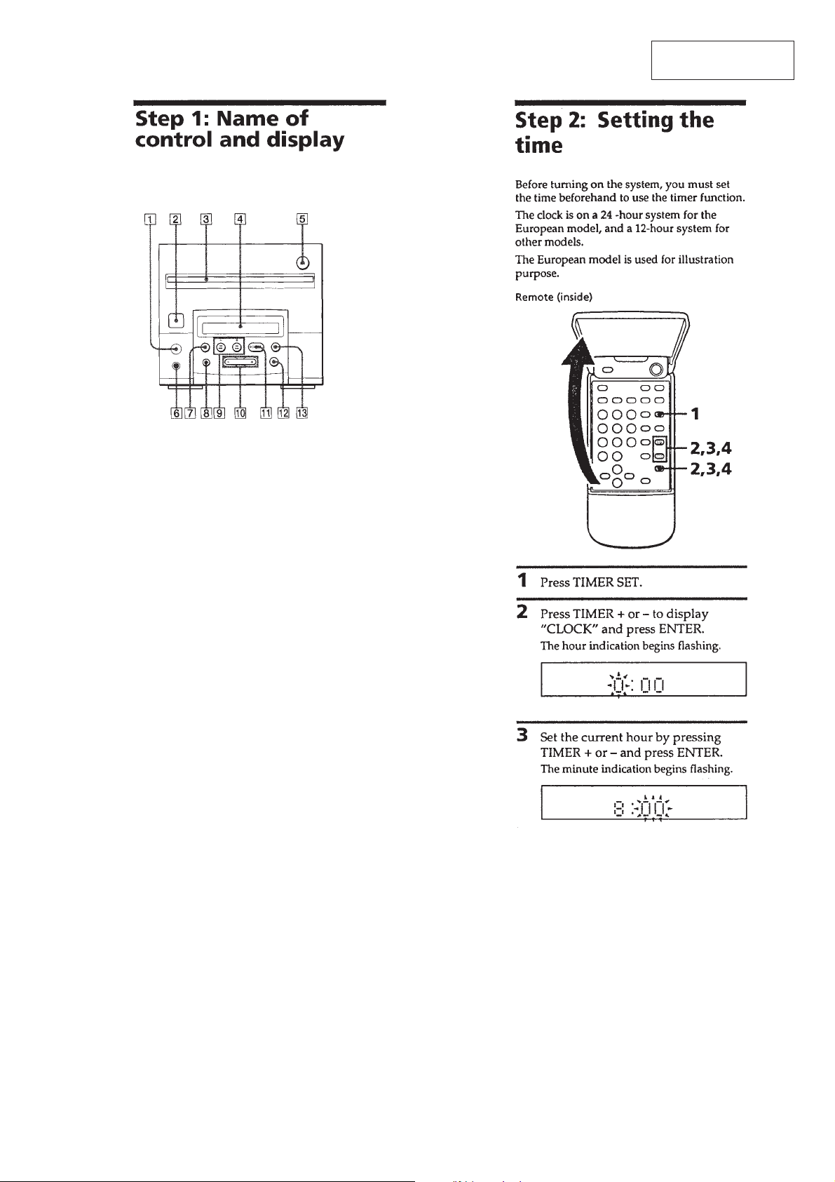
SECTION 1
GENERAL
1 Remote control signal sensor
2 Power switch
3 CD insertion slot
4 Display window
5 6 (CD EJECT) button
6 PHONES terminal
7 BAND button
8 DBFB button
9 =0/)+ (Cue-up musics, or fast rewind / fast
forward) button
0 VOL+/– button
!¡ ^ (CD playback or pause) button
!™ FUNCTION button
!£ p (CD stop) button
This section is extracted
from instruction manual.
— 3 —

2-1. CASE
1
Two screws (Case 3 TP2)
SECTION 2
DISASSEMBLY
2
Remove the case upward in the
direction of the arrow.
2-2. FRONT PANEL SECTION
claw
1
Two screws (Case 3 TP2)
3
Wire (Flat Type)
(27 Core)
2
Pull the front panel out.
4
Connector
(CN916)
1
Two screws
(BV/Ring S Tight)
— 4 —
5
Front panel section
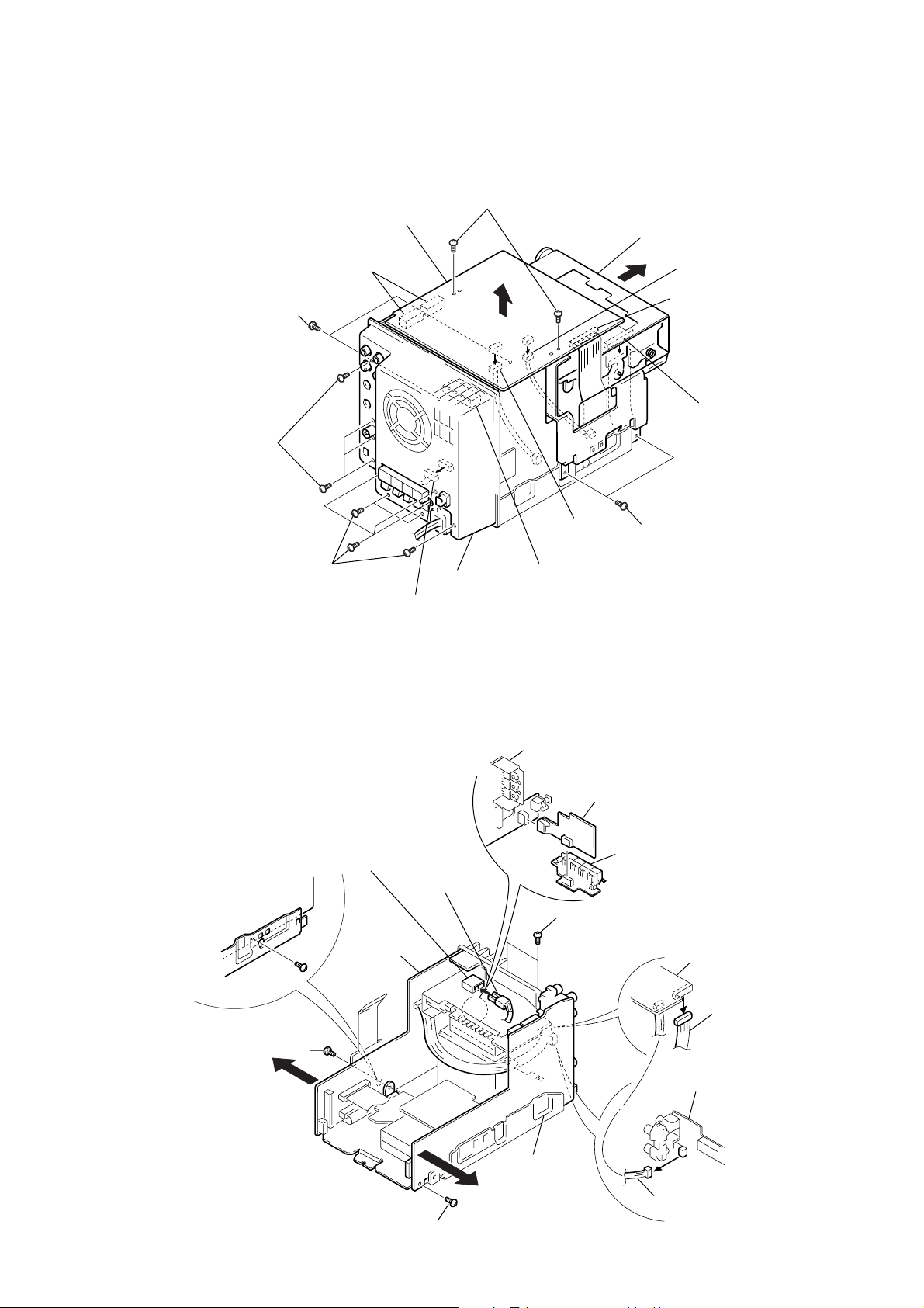
2-3. PRE board
1
Four screws
(BVTP 3
!¡
(CN420, CN422)
5
Two screws
(BVTT 3
×
8)
1
Six screws
(BVTP 3
!™
PRE board
Two Connectors
×
6)
×
8)
2
Connector
(CN814)
4
3
Back Panel
Two screws (BVTP 3×8)
!º
Connector
(CN423)
!£
Remove CN911
6-pin (Posistor board)
8
CDM50
5
Two screws
(BVTT 3
7
Connector (CN107)
9
Wire (Flat type) (21 Core)
(CN421)
6
Wire (Flat type)
(30 Core)
×
6)
2-4. FUNCTION board, RELAY board, SP TM board, TRANS board, POWER board
Power board
6
Relay board
7
SP TM board
Trans board
Function board
5
Screws
(BVTP 3
!º
Power cord (CN902)
×
8)
9
Power board
!¡
Trans board
8
Two screws (BVTT 3×6)
3
Connector (CN910)
1
Screws (BVTP 3×8)
— 5 —
4
Function board
2
Connector (CN404)
2-5. MECHANISM DECK (CDM50)
3
Mechanism Deck (CDM50)
1
Two screw (BVTT 2.6×6)
2
Bracket (CDM)
2-6. CHASSIS (T2) ASSY
3
Four screws
(BVTT 3
4
Sensor Flexible
board
1
Two screw (BVTT 2.6×6)
2
Bracket
5
Tension coil spring
1
×
6)
6
Chassis (T2) assy
Two screws
(BVTT 2.6
×
6)
— 6 —
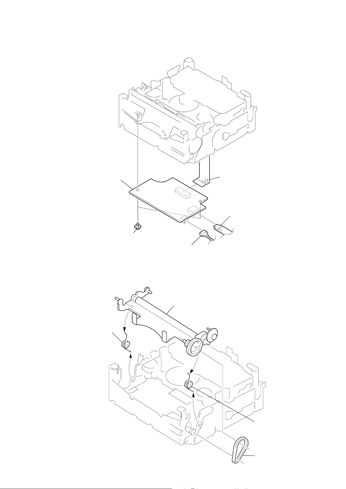
2-7. BD board
)
5
BD board
4
Flexible board
(CN101)
3
Flexible board
(CN106)
1
Two screws
(BVTT
2-8. ROLLER ARM BLOCK ASSY
1
Spring (press)
×
2)
2
Connectir (CN104)
3
Roller arm block assy
— 7 —
1
Spring (press)
2
BELT (L
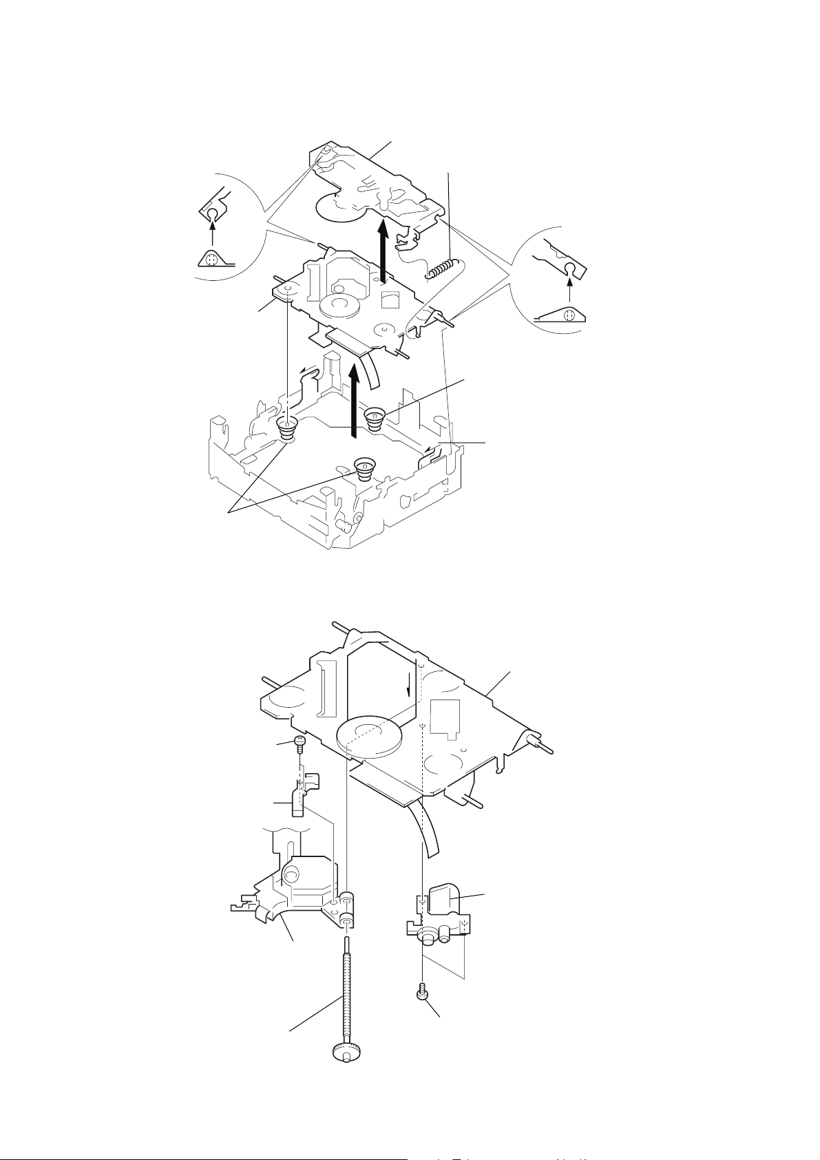
2-9. CHASSIS (OPT) ASSY, CHUCKING ARM ASSY
)
6
Move the Chucking arm assy
to the position shown in the
illustration and move it up.
2
Chassis (OPT)
assy
7
Chucking arm assy
5
Spring (CH)
6
Move the Chucking arm assy
to the position shown in the
illustration and move it up.
4
Spring (FL2)
A
Two Spring (FL)
3
2-10. MOTOR (SL) ASSY (M102), OPTICAL PICK-UP (KSS-313A)
A
4
Screws
(+P 1.7
5
Gear (SL Feed)
×
4)
1
Move the lever in the
direction of arrow (A).
7
Chassis (OPT) assy
6
Optical Pick-Up
(KSS-313A)
3
Move the shift (SL)
assy in the direction
of arrow
A
remove
it from chassis (OPT)
and optical Pick-up.
1
Two screws (+BVTT 3×6)
— 8 —
2
Motor (SL)assy (M102

SECTION 3
TEST MODE
There are two methods to enter the TEST mode.
• How to Enter the Test Mode - 1
Remove the AC power cord from wall outlet, and press [EJECT
6]. While pressing [EJECT 6], connect the AC power cord to
wall outlet.
• How to Enter the Test Mode - 2
(This method toggles between “Entering the TEST Mode” and
“Exiting the TEST Mode”.)
Turn on the main power. While pressing [TUNING +], press
[DBFB], release hand from [DBFB] then press [FUNCTION].
(Keep pressing [TUNING] all the way.)
Pressing these buttons again in the same order exits the TEST
mode.
* The small ATT segment lights in the center top of display during
the TEST mode.
* T o exit the TEST mode, disconnect the AC po wer cord from wall
outlet, or use “How to Enter the TEST Mode - 2”.
1. Audio volume control setting (Can be adjusted only during TEST
mode.)
Press [CD STOP p] and [VOL–] at the same time
→ VOL MINIMUM appears
Press [CD STOP p] and [VOL+] at the same time
→ VOL MAXIMUM appears
* The audio volume data is kept stored even after the main power
is turned off.
2. Audio balance setting (Can be adjusted only during TEST
mode.)
Press [CD STOP p] and [DBFB] at the same time
→ LEFT 10 appears
Press [CD STOP p] and [FUNCTION] at the same time
→ RIGHT 10 appears
Press [CD STOP p] and [CD EJECT 6] at the same time
→ CENTER appears
* The audio balance data is kept stored even after the main power
is turned off.
5. Watch operation check (Can be operated only while the main
power is off.)
Press [FUNCTION] and [BAND] at the same time. → Watch
starts counting.
Various CD tests
Pressing the two keys at the same time enables the various
adjustment and test as follows in the TEST mode, and “ATT”
segment is flashing.
1) Pressing [TUNING–] and [CD EJECT 6] at the same time :
The present normal tracking balance value (“31” to “36”) is
displayed when the above key operation is performed and
(TRBAL.) is displayed.
The tracking gain is fixed to “3F” (TOG1 to TOG2: all off)
2) Pressing [TUNING–] and [DBFB] at the same time :
(SHUFFLE) is displayed.
• ADJUSTMENT mode
When the above key operation is performed, the machine
enters the ADJUSTMENT mode. The “SHUFFLE” flashes
on display tube.
During the ADJUSTMENT mode:
The CLV gain is not switched to 8 cm. (The CLV gain is
fixed to 12 cm always.)
The machine is ready to enter the AF-ADJUSTMENT mode
as described below.
3) Pressing [TUNING–] and [FUNCTION] at the same time :
(SHUFFLE) and (PROGRAM) are displayed.
• AF-ADJUSTMENT mode
After the machine enters the ADJUSTMENT mode by the
key operation as described in step 2), the machine can enter
the AF-ADJUSTMENT mode by pressing the above key
operation. [TUNING – /FUNCTION]
The “SHUFFLE” and “PROGRAM” flash on display.
3. Key test and FL display tube test (Can be adjusted only during
TEST mode.)
• Press [VOL-] and [BAND] at the same time→All FL tubes
light. Pressing the following key in this status enables key
checks as follows.
• Display depending upon the pressed key
[FUNCTION] → KEY NO. 1
[VOL –] → KEY NO. 2
[VOL +] → KEY NO. 3
[BAND] → KEY NO. 4
[TUNING+] → KEY NO. 5
[EJECT 6] → KEY NO. 6
[TUNING –] → KEY NO. 7
[STOP p] → KEY NO. 8
[PLAY ^] → KEY NO. 9
[DBFB] → KEY NO. 10
• [POWER] → Returns to the TEST mode
* Note: After all keys are (KEY No.1 to KEY No.10) tested,
CHECK OK!! appears.
The following items have no relation with the TEST mode.
4. Initial setting (All clear of all memories)
Disconnect the AC power cord. While pressing [POWER],
connect the AC power cord to wall outlet.
During the AF-ADJUSTMENT mode, the tracking and sled
servos are turned off in addition to the ADJUSTMENT mode.
The machine stops the GFS error check which is normally
performed by software.
• Sled motor check
When disc is removed by pressing EJECT during the AFADJUSTMENT mode, the sled can be moved to inner
circumference or outer circumference by pressing [TUNING–
] or [TUNING+]. At this time, because the microprocessor
is not sensing the sled position, be careful when moving the
sled not to damage gears and other mechanism.
4) Pressing [TUNING–] and [VOL–] at the same time :
• No CDM mode
[1] is displayed.
When the above key operation is performed, the control on
the slot mechanism which takes in and ejects a CD disc is
stopped.
At this time “1” on the display flashes.
During the no CDM mode,
The TOC data is deleted by the [CD EJECT 6] key.
(When the TEST mode is cleared and a CD disc is inserted,
machine reads the TOC again.)
— 9 —

5) Pressing [TUNING–] and [VOL+] at the same time :
• Aging mode
The machine enters the aging mode by inserting a CD disc
and performing the above button
operation. The display starts counting the aging operation
with COUNT display, and “REPEAT” flashes.
Aging operation
1. Machine takes a disc into the machine.
2. Reads the TOC.
3. Accesses to the last track.
4. Plays back the last 2 seconds.
5. Ejects the disc.
The one complete operation from step 1 to step 5 is one count.
The cycle is repeated. However, steps 2 to 4 are skipped in all
modes other than the CD function.
Steps 1 and 5 are skipped in the no CDM mode.
The aging operation ends when an error occurs.
Aging error display
“Load Error” : Loading operation is not completed in four
seconds.
“Eject Error” : Eject operation is not completed in four
seconds.
“Q TOC Err” : The Q data could not be read during eight
seconds. (During TOC read)
“Q SRCH Err” : The Q data could not be read during eight
seconds. (During track search)
“Q PLAY Err” : The Q data could not be read during eight
seconds. (During PLAY)
“FOK UP Err” : Focus could not be locked in. (During
setup)
“FOK TOC Err” : Focus is un-locked many times. (During
TOC read)
“FOK SRCH Err” : Focus is un-locked many times. (During
track search)
“FOK PLAY Err” : Focus is un-locked several times. (During
play)
“GFS UP Err” : GFS error. (During setup)
“GFS TOC Err” : GFS error. (During TOC read)
“GFS PLAY Err” : GFS error. (During play)
** Other troubles
“TW*SW*”
TW : Numbers of times that the machine could not read
TOC.
SW : Numbers of times that the machine could not
complete the track search within 16 seconds.
To exit the aging mode and to return the TEST mode, press
[TUNING – ] and [VOL +] at the same time.
Display selection during aging
The display can be switched by pressing the [TUNING–] and
[FUNCTION] at the same time :
Example of display
Count display
Elapsed time display
Other errors
Normal display
" COUNT 723 " (Machine has repeated for 723 times.)
" 12 : 05 : 35 " (12 hours 5 minutes 35 seconds have elapsed.)
" TW 2 SW 1 "
— 10 —
V
A
B
symmetry
within 2.4
±
0.7 Vp-p
+
–
BD board
TP (RF)
TP (VC)
oscilloscope
V
SECTION 4
ELECTRICAL ADJUSTMENTS
CD SECTION
Note:
1. CD Block is basically constructed to operate without adjustment.
Therefore, check each item in order given.
2. Use YEDS-18 disc (3-702-101-01) unless otherwise indica ted.
3. Use the oscilloscope with more than 10MΩ impedance.
4. Clean an object lens by an applicator with neutral detergent
when the signal level is low than specified value with the
following checks.
5. When optical pickup is replaced during repair, perform the focus
bias adjustment.
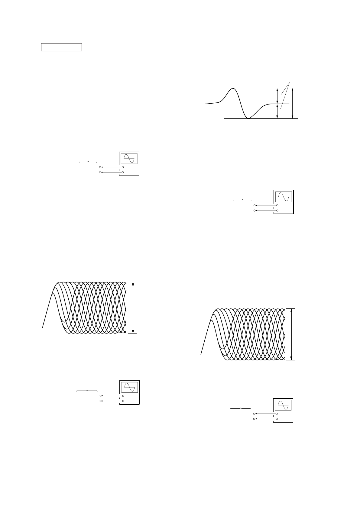
Focus Bias Adjustment
oscilloscope
(DC range)
BD board
TP (RF)
TP (VC)
+
–
This adjustment is to be done when the optical block is replaced.
Adjustment procedure:
1. Connect oscilloscope to test point TP (VC) and TP (RF) on BD
board.
2. Turned power switch ON. (Stop state)
3. Insert disc (YEDS-18) and press the ^ button.
4. Adjust R V101 so that the oscilloscope wav eform is as shown in
the figure below (eye pattern).
A good eye pattern means that the diamond shape (≈) in the
center of the waveform can be clearly distinguished.
• RF signal reference waveform (eye pattern)
VOLT/DIV: 200 m
TIME/DIV: 500 ns
5. Check the oscilloscope waveform (S-curve) is symmetrical
between A and B. And conf irm that peak to peak le vel is within
2.4 ± 0.7 Vp-p.
S-curve waveform
6. After check, remove the lead wire connected in step 2.
Note: • Try to measure several times to make sure that the ratio of
A:B or B:A is more than 10:7.
• Select a longer sweep time and increase the brightness to
obtain best waveform.
RF Level Check
Procedure:
1. Connect oscilloscope to test point TP (VC) and TP (RF) on BD
board.
2. Turned Power switch on.
3. Insert the disc (YEDS-18) and press the ^ button.
4. Confirm that oscilloscope waveform is clear and check RF signal
level is correct.
Note: Clear RF signal waveform means that the shape “≈” can be
clearly distinguished at the center of the waveform.
RF signal waveform
level:
1.3
±
0.3Vp-p
When observing the eye pattern, set the oscilloscope for AC
range and raise vertical sensitivity.
S-Curve Check
oscilloscope
BD board
TP (FEO)
TP (VC)
+
–
Procedure:
1. Connect as oscilloscope to test point TP (VC) and TP (FEO) on
BD board.
2. Connect a lead wire between test point TP (FOK) and Ground.
3. Turned Power switch on.
4. Insert disc (YEDS-18) and turned Power switch on again to
actuate the focus search. (actuate the focus search when disc
table is moving in and out.)
E-F Balance (Traverse) Check
Procedure:
1. Set up the TEST mode step 3) AF-ADJUSTMENT. (see page
2. Connect as oscilloscope to test point TP (TEO) on BD board.
3. Turned Power switch on.
4. Insert the disc (YEDS-18) in and press the ^ button.
5. Confirm that the oscilloscope waveform is symmetrical on the
— 11 —
VOLT/DIV: 200 m
TIME/DIV: 500 ns
level:
±
0.3Vp-p
1.3
oscilloscope
(DC range)
BD board
TP (TEO)
TP (VC)
+
–
9.)
top and bottom in relation to 0V dc, and check the amplitude.
Traverse waveform
y
symmetr
A
0 V
B
amplitude: 300 ± 100 mVp-p
specified value:
A-B
×
•
2 (A+B)
•
A+B = 300 ± 100 mVp-p
100 = less than ± 7%
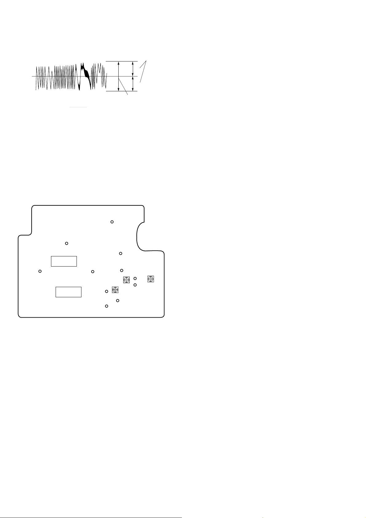
Focus/Tracking Gain Adjustment
This gain has a margin, so even if it is slightly off. There is no
problem.
Therefore, do not perform, RV102 and RV103 adjustment.
Please note that it should be fixed to mechanical center position
when you moved and do not know original position.
Adjustment Location:
[BD BOARD] — Component side —
(RF)
(PCK)
(VC)
IC102
IC104
(FOK)
(FEO)
(TAO)
(A.GND)
(D.GND)
RV103
RV102
(FEI)
(TEO)
RV101
(TEI)
— 12 —

— 13 —
 Loading...