

Page 1
DSR-PD100/PD100P
SERVICE MANUAL
Ver 1.5 2003. 05
RMT-811
US Model
Canadian Model
DSR-PD100
AEP Model
DSR-PD100P
C MECHANISM
NTSC model: DSR-PD100
PAL model: DSR-PD100P
Photo: DSR-PD100
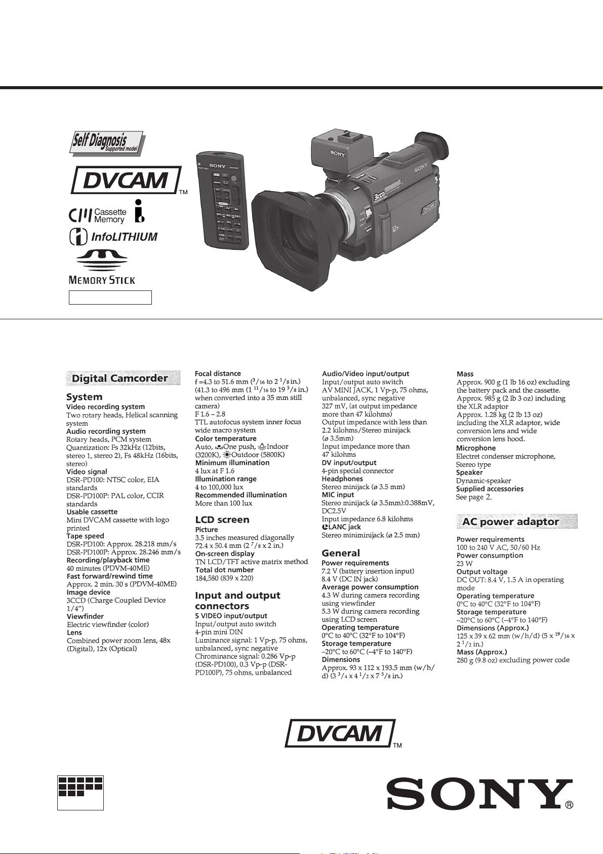
SPECIFICATIONS
MICROFILM
— Continued on next page —
DIGITAL CAMCORDER
Page 2
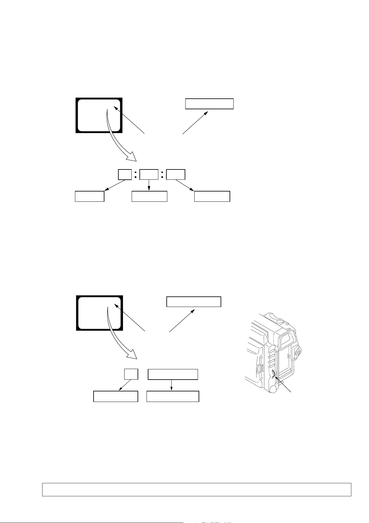
SELF-DIAGNOSIS FUNCTION
Control dial
1. SELF-DIAGNOSIS FUNCTION
When problems occur while the unit is operating, the self-diagnosis
function starts working, and displays on the viewf inder, LCD screen
or LCD window what to do. This function consists of two display;
self-diagnosis display and service mode display.
Details of the self-diagnosis functions are provided in the Instruction
manual.
Viewfinder or LCD screen LCD window
C : 3 1 : 1 1
Blinks at 3.2Hz
1 1
Repaired by:
C : Corrected by customer
H : Corrected by dealer
E : Corrected by service
engineer
C
Indicates the appropriate
step to be taken.
E.g.
31 ....Reload the tape.
32 ....Turn on power again.
3 1
Block
2. SELF-DIAGNOSIS DISPLAY
When problems occur while the unit is operating, the counter of the
viewfinder, LCD screen or LCD window consists of an alphabet
and 4-digit numbers, which blinks at 3.2 Hz. This 5-character display
indicates the “repaired by:”, “block” in which the problem occurred,
and “detailed code” of the problem.
C : 3 1 : 11
Detailed Code
Refer to page 8.
Self-diagnosis Code Table.
3. SERVICE MODE DISPLAY
The service mode display shows up to six self-diagnosis codes shown in the past.
3-1. Display Method
While pressing the “STOP” key, set the switch from OFF to “VTR or PLAYER”, and continue pressing the “STOP” key for 5 seconds
continuously. The service mode will be displayed, and the counter will show the backup No. and the 5-character self-diagnosis codes.
Viewfinder or LCD screen
[3] C : 3 1 : 1 1
Lights up
[3]
Backup No.
Order of previous errors
C : 3 1 : 1 1
Self-diagnosis Codes
3-2. Switching of Backup No.
By rotating the control dial, past self-diagnosis codes will be shown in order. The backup No. in the [] indicates the order in which the
problem occurred. (If the number of problems which occurred is less than 6, only the number of problems which occurred will be shown.)
[1] : Occurred first time [4] : Occurred fourth time
[2] : Occurred second time [5] : Occurred fifth time
[3] : Occurred third time [6] : Occurred the last time
LCD window
3 C : 3 1 : 11
3-3. End of Display
Turning OFF the power supply will end the service mode display.
Note: The “self-diagnosis display” data will be backed up by the coin-type lithium battery of CK-80 board BT7200. When this coin-type lithium battery
is removed, the “self-diagnosis display” data will be lost by initialization.
— 7 —
Page 3

4. SELF-DIAGNOSIS CODE TABLE
Self-diagnosis Code
Repaired by:
C
C
C
C
C
C
C
C
C
C
C
C
C
C
C
C
C
C
C
C
C
C
C
E
E
E
E
Block
Function
21
22
23
31
31
31
31
31
31
31
31
31
31
31
31
32
32
32
32
32
32
32
32
61
61
62
62
Detailed
Code
00
00
00
10
11
20
21
22
23
24
30
40
42
10
11
20
21
22
23
24
30
40
42
00
10
00
01
Symptom/State
Condensation.
Video head is dirty.
Non-standard battery is used.
LOAD direction. Loading does not
complete within specified time
UNLOAD direction. Loading does not
complete within specified time
T reel side tape slacking when unloading
Winding S reel fault when counting the
rest of tape.
T reel fault.
S reel fault.
T reel fault.
FG fault when starting capstan.
FG fault when starting drum.
FG fault during normal drum operations.
LOAD direction loading motor time-
out.
UNLOAD direction loading motor
time-out.
T reel side tape slacking when
unloading.
Winding S reel fault when counting the
rest of tape.
T reel fault.
S reel fault.
T reel fault.
FG fault when starting capstan.
FG fault when starting drum
FG fault during normal drum
operations
Difficult to adjust focus
(Cannot initialize focus.)
Zoom operations fault
(Cannot initialize zoom lens.)
Steadyshot function does not work well.
(With pitch angular velocity sensor output
stopped.)
Steadyshot function does not work well.
(With yaw angular v elocity sensor output
stopped.)
Correction
Remove the cassette, and insert it again after one hour.
Clean with the optional cleaning cassette.
Use the info LITHIUM battery.
Load the tape again, and perform operations from the beginning.
Load the tape again, and perform operations from the beginning.
.
Load the tape again, and perform operations from the beginning.
Load the tape again, and perform operations from the beginning.
Load the tape again, and perform operations from the beginning.
Load the tape again, and perform operations from the beginning.
Load the tape again, and perform operations from the beginning.
Load the tape again, and perform operations from the beginning.
Load the tape again, and perform operations from the beginning.
Load the tape again, and perform operations from the beginning.
Remove the battery or power cable, connect, and perform
operations from the beginning.
Remove the battery or power cable, connect, and perform
operations from the beginning.
Remove the battery or power cable, connect, and perform
operations from the beginning.
Remove the battery or power cable, connect, and perform
operations from the beginning.
Remove the battery or power cable, connect, and perform
operations from the beginning.
Remove the battery or power cable, connect, and perform
operations from the beginning.
Remove the battery or power cable, connect, and perform
operations from the beginning.
Remove the battery or power cable, connect, and perform
operations from the beginning.
Remove the battery or power cable, connect, and perform
operations from the beginning.
Remove the battery or power cable, connect, and perform
operations from the beginning.
Inspect the lens block focus reset sensor (Pin !º of CN500 of VC-
208 board) when focusing is performed when the control dial is
rotated in the focus manual mode, and the focus motor drive circuit
(IC500 of VC-208 board) when the focusing is not performed.
Inspect the lens block zoom reset sensor (Pin !™ of CN500 of VC208 board) when zooming is performed when the zoom lens is
operated and the zoom motor drive circuit (IC500 of VC-208 board)
when zooming is not performed.
Inspect pitch angular velocity sensor (SE451 of SE-75 board)
peripheral circuits.
Inspect yaw angular velocity sensor (SE450 of SE-75 board)
peripheral circuits.
— 8 —
Page 4
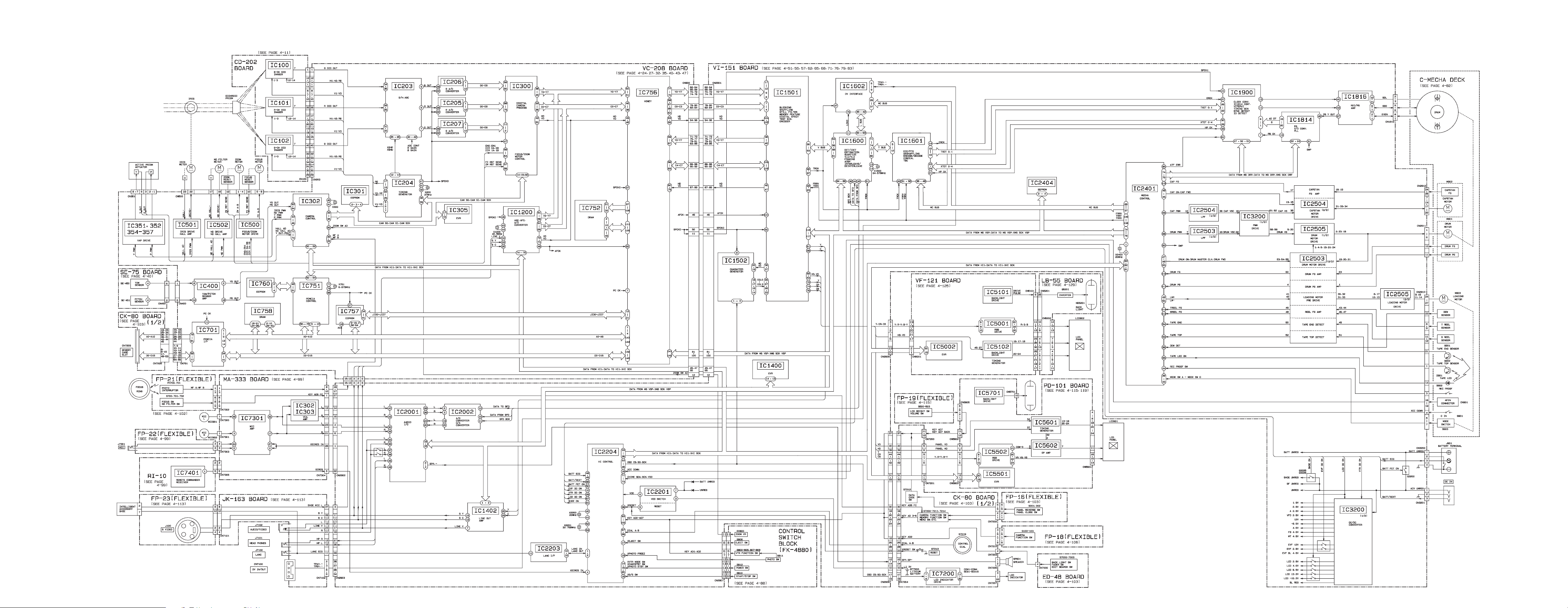
3-1. OVERALL BLOCK DIAGRAM
SECTION 3
DSR-PD100/PD100P
BLOCK DIAGRAMS
3-1 3-2 3-3 3-4
Page 5
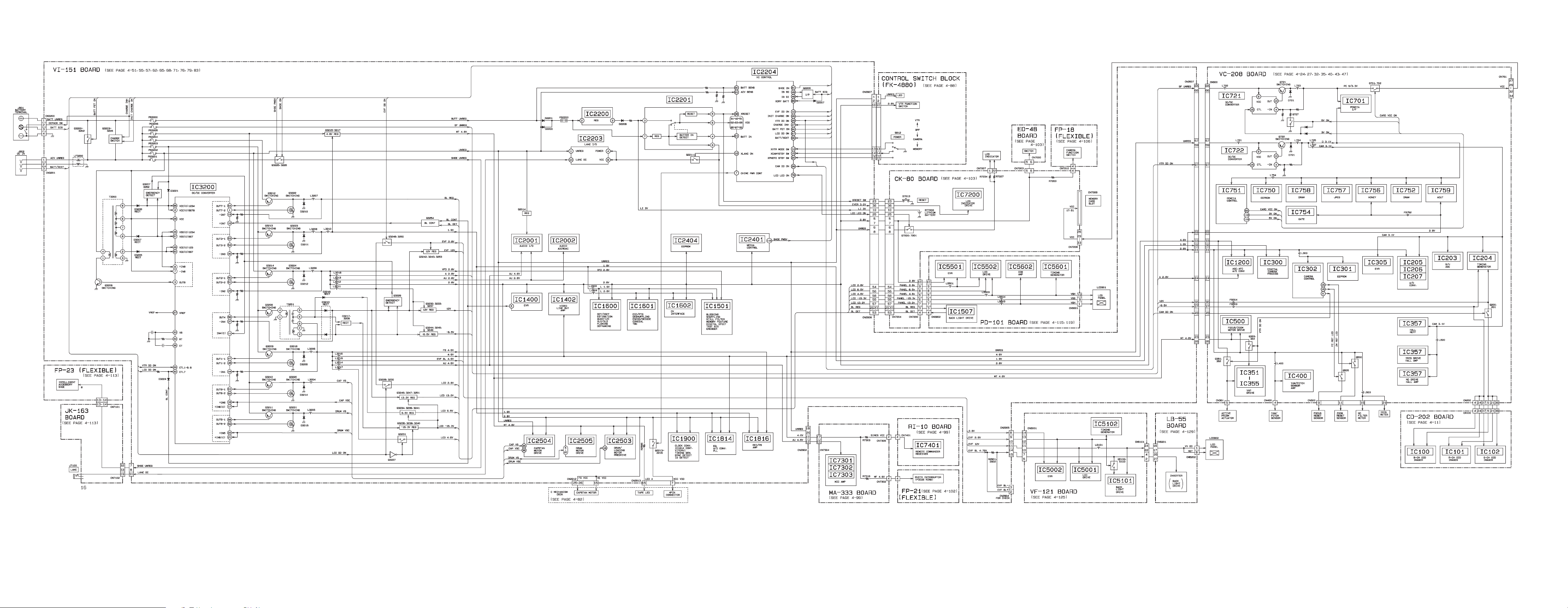
DSR-PD100/PD100P
3-2. POWER BLOCK DIAGRAM
3-5 3-6 3-7 3-8E
Page 6
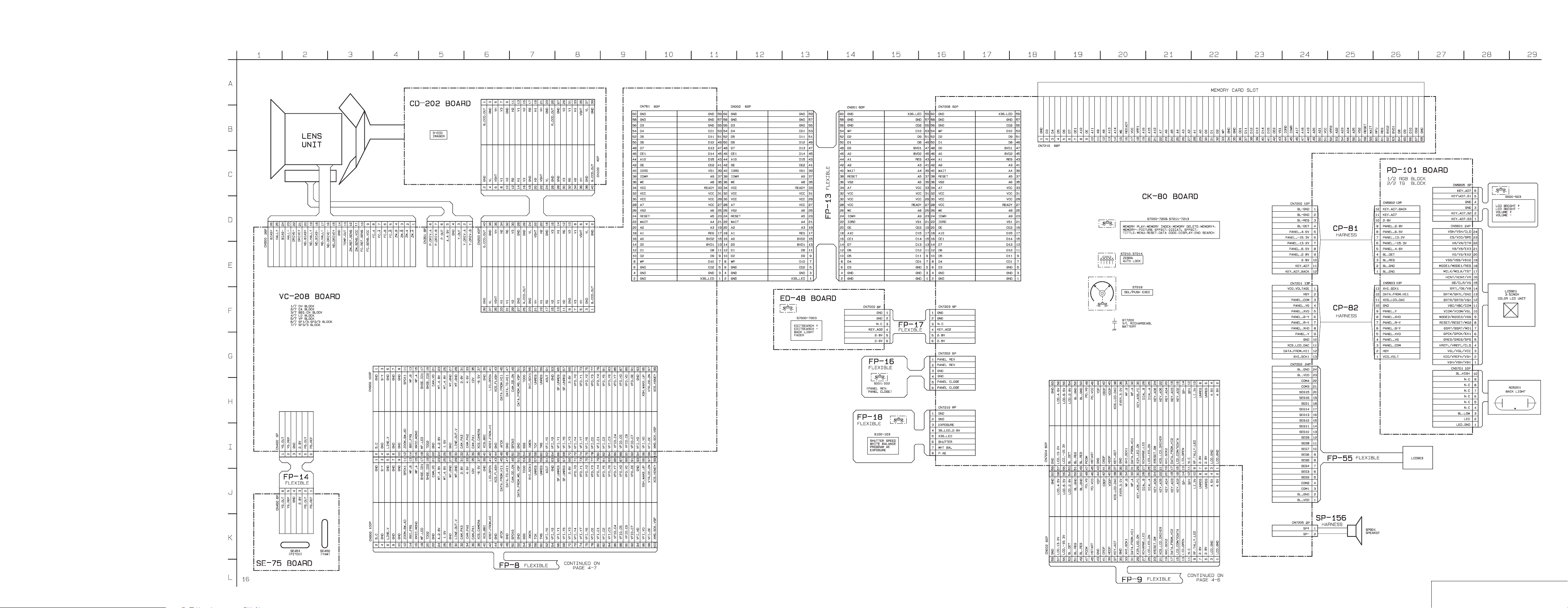
PRINTED WIRING BOARDS AND SCHEMATIC DIAGRAMS
4-1. FRAME SCHEMATIC DIAGRAM-1
SECTION 4
DSR-PD100/PD100P
4-1 4-2 4-3 4-4
FRAME SCHEMATIC DIAGRAM-1
Page 7
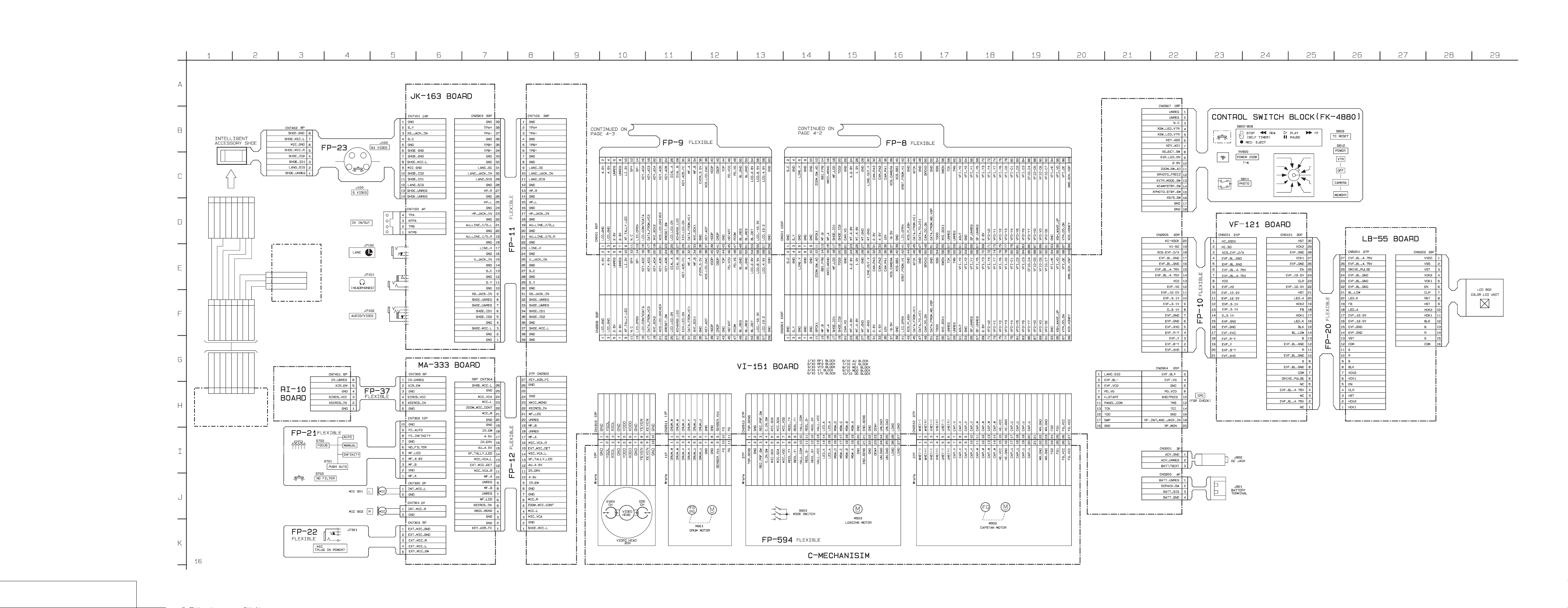
DSR-PD100/PD100P
FRAME SCHEMATIC DIAGRAM-2
8765432
XL-51 HARNESS
SHOE UNREG
LANC SIG
SHOE ID1
SHOE ID 2
8765432
SHOE UNREG
SHOE ID1
MIC GND
SHOE MIC L
SHOE UNREG
SHOE ID1
MIC GND
SHOE MIC L
8765432
CN101
8P
SHOE MIC R
MIC GND
SHOE MIC L
SHOE GND
DD GND
+46V
SHOE GND
DD GND
+46V
PLUG
1
CONNECTOR
SHOE GND
1
2
3
1
DD UNREG
DD UNREG
1
DD-120
BOARD
DD UNREG
+46V
DD GND
CN201
3P
FRAME SCHEMATIC DIAGRAM-2
XL-2 BOARD
4-5 4-6 4-7 4-8
Page 8
4-2. PRINTED WIRING BOARDS AND SCHEMATIC DIAGRAMS
THIS NOTE IS COMMON FOR WIRING BOARDS AND SCHEMATIC DIAGRAMS
(In addition to this, the necessary note is printed in each block)
DSR-PD100/PD100P
DSR-PD100/PD100P
(For printed wiring boards)
• b: Pattern from the side which enables seeing.
(The other layers' patterns are not indicated.)
• Through hole is omitted.
• Circled numbers refer to waveforms.
• There are few cases that the part printed on diagram
isn’t mounted in this model.
• Chip parts.
Transistor Diode
C
5
BE
64
2
13
5
46
2
31
45
2
31
12
4
53
3
21321321
(For schematic diagrams)
• All capacitors are in µF unless otherwise noted. pF : µµF.
50V or less are not indicated except for electrolytics and
tantalums.
• Chip resistors are 1/10W unless otherwise noted.
kΩ=1000Ω, MΩ=1000kΩ.
• Caution when replacing chip parts.
New parts must be attached after removal of chip.
Be careful not to heat the minus side of tantalum capacitor, Because it is damaged by the heat.
• Some chip part will be indicated as follows.
Example C541 L452
22U 10UH
TA A 2520
Kinds of capacitor
Temperature characteristics
External dimensions (mm)
• Constants of resistors, capacitors, ICs and etc with XX indicate
that they are not used.
In such cases, the unused circuits may be indicated.
• Parts with ★ differ according to the model/destination.
Refer to the mount table for each function.
• All variable and adjustable resistors have characteristic curve B,
unless otherwise noted.
• Signal name
XEDIT→ EDIT PB/XREC → PB/REC
• 2 : non flammable resistor
• 1 : fusible resistor
• C : panel designation
• A : B+ Line *
• B : B– Line *
• J : IN/OUT direction of (+,–) B LINE. *
• C : adjustment for repair. *
• Circled numbers refer to waveforms. *
*Indicated by the color red.
Note :
The components identified by
mark ! or dotted line with mark
! are critical for safety.
Replace only with part number
specified.
Note :
Les composants identifiés par
une marque ! sont critiques
pour la sécurité.
Ne les remplacer que par une
pièce portant le numéro spécifié.
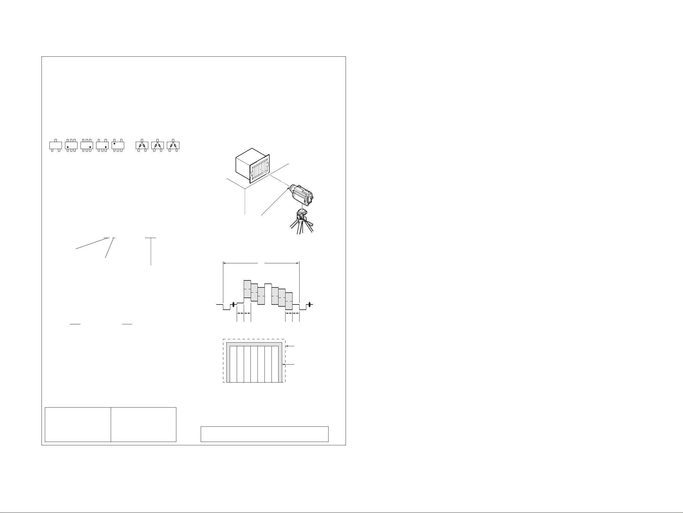
(Measuring conditions voltage and waveform)
• Voltages and waveforms are measured between the measurement points and ground when camera shoots color bar chart of
pattern box. They are reference values and reference waveforms. *
(VOM of DC 10 MW input impedance is used.).
• Voltage values change depending upon input impedance of VOM
used.)
1. Connection
Pattern box
95 cm
Front side of the lens
2. Adjust the distance so that the output waveform of Fig. a and
the Fig. b can be obtain.
H
Yellow
Cyan
White
Magenta
Green
AABBA=B
Fig. a (Video output terminal output waveform)
Cyan
White
Green
Yellow
Magenta
Fig.b (Picture on monitor TV)
3. • The LINE REC w avefo rm shows the wavef orm when the color
for signal (video signal) is input from a color bar pattern.
• The LINE OUT waveform shows the wavefor m when the
signals are connected to the S-VIDEO and VIDEO/AUDIO
jacks but not to other jacks.
When indicating parts by reference number, pleas include
the board name.
Red
Blue
Red
Blue
Electron beam
scanned frame
CRT picture frame
4-9
Page 9
DSR-PD100/PD100P
CD-202
CAMERA REC
IC100 1, 2
1
IC101 1, 2
IC102 1, 2
IC100 3, IC101 3
2
IC102 3
IC100 !£, !¢
3
IC101 !£, !¢
IC102 !£, !¢
13.5 MHz
IC100 !™, IC101 !™
4
IC102 !™
BOARD
H
V
8.4Vp-p
22Vp-p
3.0Vp-p
5
Q101 E
6
Q100 E
7
Q102 E
13.5 MHz
H
H
H
H
H
3.0Vp-p
0.6Vp-p
0.6Vp-p
0.5Vp-p
CCD IMAGER
CD-202
4-11 4-12
Page 10
DSR-PD100/PD100P
DSR-PD100/PD100P
For schematic diagram
• Refer to page 4-17 for printed wiring board.
VC-208
1
CAMERA REC
2
CAMERA REC
3
CAMERA REC
4
CAMERA REC
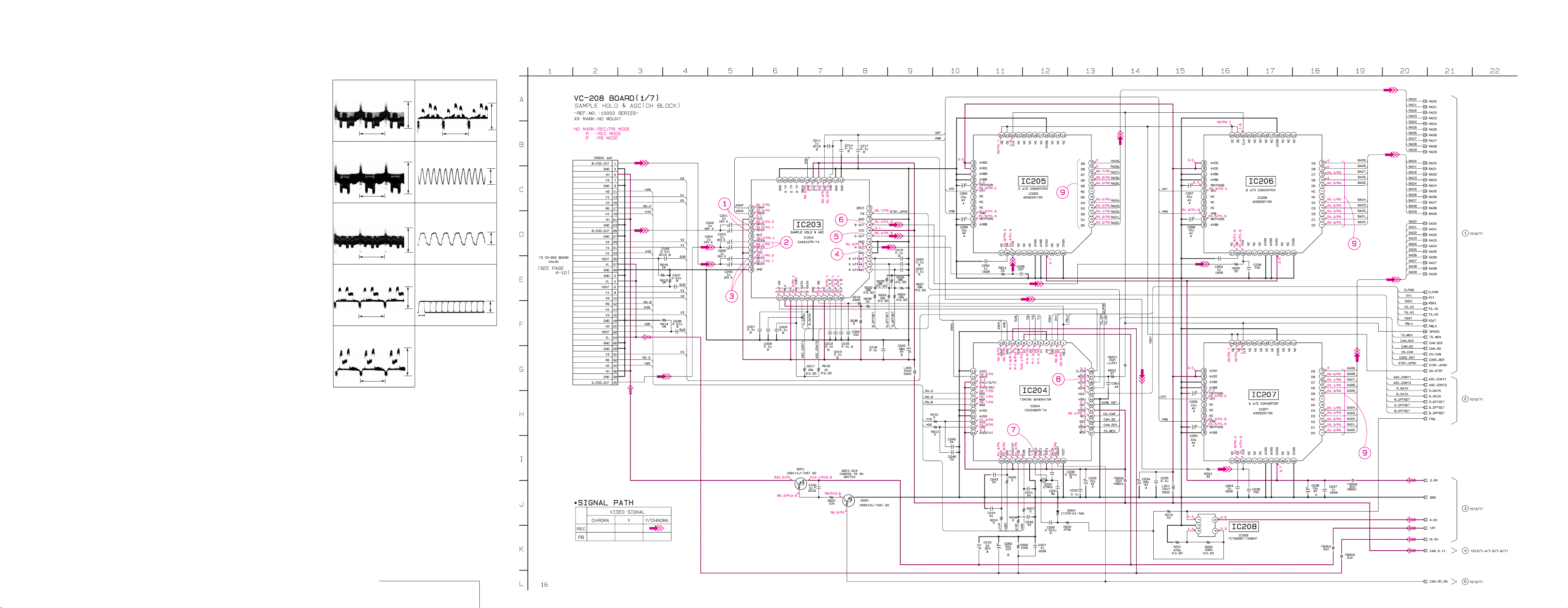
BOARD (1/7)
IC203 @•, @ª
H
IC203 #¡, #™
H
IC203 #¢, #∞
H
IC203 5
6
0.6Vp-p
0.5Vp-p
0.6Vp-p
IC203 9
CAMERA REC
7
IC204 #¡
CAMERA REC
8
IC204 $¶
CAMERA REC/PB
9
IC205 1 – 5 , 8 – !™
IC206 1 – 5 , 8 – !™
IC207 1 – 5 , 8 – !™
CAMERA REC
H
27.0 MHz
13.5 MHz
0.34Vp-p
3.4Vp-p
3.0Vp-p
H
5
IC203 7
CAMERA REC
H
0.28Vp-p
0.34Vp-p
74 nsec
2.8Vp-p
SAMPLE HOLD & AGC
VC-208 (1/7)
4-24 4-25 4-26
Page 11
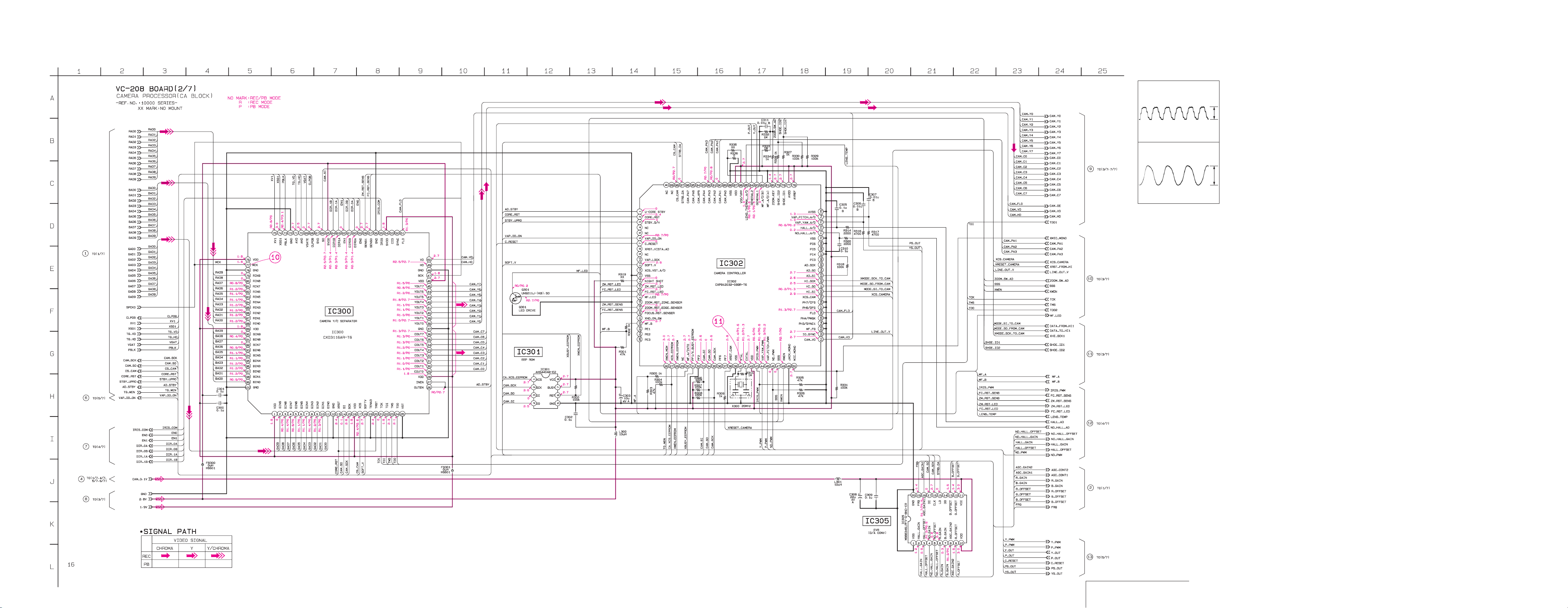
For schematic diagram
• Refer to page 4-17 for printed wiring board.
DSR-PD100/PD100P
DSR-PD100/PD100P
VC-208
!º
CAMERA REC/PB
!¡
CAMERA REC/PB
BOARD (2/7)
IC300 &¶
13.5MHz
IC302 $º
20.0MHz
3.0Vp-p
2.8Vp-p
4-27 4-28 4-29
CAMERA PROCESSOR
VC-208 (2/7)
Page 12

DSR-PD100/PD100P
DSR-PD100/PD100P
For schematic diagram
• Refer to page 4-17 for printed wiring board.
VC-208
BOARD (3/7)
!™ IC1200 @∞
LINE REC (NTSC)
H
!™ IC1200 @∞
CAMERA REC/PB
H
!£ IC1200 #£
LINE REC (NTSC)
H
!£ IC1200 #£
CAMERA REC/PB
0.44Vp-p
1.0Vp-p
0.5Vp-p
H
1.5Vp-p
!¢ IC1200 #¢
LINE REC (NTSC)
H
0.44Vp-p
!¢ IC1200 #¢
CAMERA REC/PB
2.0Vp-p
3.0Vp-p
IC1200 $¢
!∞
LINE REC
40.5MHz
H
!§ IC1200 ^¡ – ^•
CAMERA REC/PB,
LINE REC
4-31
74 nsec
2.8Vp-p
BASE BAND INPUT
VC-208 (3/7)
4-32 4-33 4-34
Page 13

For schematic diagram
• Refer to page 4-17 for printed wiring board.
DSR-PD100/PD100P
DSR-PD100/PD100P
4-35 4-36
4-37
MOTOR DRIVE
VC-208 (4/7)
Page 14

DSR-PD100/PD100P
)
SE-75 (YAW/PITCH SENSOR) PRINTED WIRING BOARD
— Ref. No. SE-75 Board; 10,000 Series —
SE-75 BOARD
C450 B-2
C451 A-2
CN450 A-2
L450 B-1
SE450 B-2
SE451 C-1
For schematic diagram
• Refer to page 4-17 for printed wiring board of VC-208.
For printed wiring boards
• This board is six-layer print board. However, the patterns of layers two to five have not been included in
the diagram.
There are few cases that the part printed on this
diagram isn’t mounted in this model.
LB-55
(EVF BACK-LIGHT)
VF-121
(COLOR EVF)
ED-48
(USER CONTROL)
SE-75
(YAW/PITCH SENSOR)
JK-163
(AUDIO/VIDEO IN/OUT)
RI-10
(SIRCS RECEIVER)
MA-333
(STEREO MIC AMP)
CK-80
USER CONTORL,
LCD DRIVE
PD-101
(RGB DRIVER, TIMING GENERATOR, BACK-LIGHT
1-670-999-
12
VAP DRIVER
VC-208 (5/7)
YAW/PITCH SENSOR
/
SE-75
4-39 4-40 4-41 4-42
Page 15

For schematic diagram
• Refer to page 4-17 for printed wiring board.
DSR-PD100/PD100P
VC-208 BOARD (6/7)
CAMERA REC/PB
!¶ IC722 !º
2.3µsec
0.8Vp-p
4-43 4-44 4-45 4-46
CARD CONTROL, PWM CONTROL
VC-208 (6/7)
Page 16

DSR-PD100/PD100P
For schematic diagram
• Refer to page 4-17 for printed wiring board.
HONEY, PCMCIA CONTROL
VC-208 (7/7)
4-47 4-48 4-49 4-50
VC-208
!•
CAMERA REC/PB
BOARD (7/7)
IC751 &¶
6.85MHz
3.8Vp-p
Page 17

For schematic diagram
• Refer to page 4-91 for printed wiring board.
DSR-PD100/PD100P
VI-151 BOARD (1/10)
1 IC1816 1, 2, 6, 7
CAMERA REC
6.8msec
3.5Vp-p
2 IC1816 !¡, !™
CAMERA REC
6.8msec
2.0Vp-p
3 IC1816 @¶ PB
0.35Vp-p
6.8msec
4 IC1816 $º
CAMERA REC/PB
41.7MHz
5 IC1816 $™
CAMERA REC
25nsec
6 IC1814 !£ PB
41.85MHz
7 IC1814 !∞ – @º PB
25nsec
2.3Vp-p
2.2Vp-p
2.0Vp-p
2.2Vp-p
4-51 4-52 4-53
8 IC1814 #¡
CAMERA REC/PB
6.8msec
2.6Vp-p
REC/PB AMP
VI-151 (1/10)
Page 18

DSR-PD100/PD100P
DSR-PD100/PD100P
For schematic diagram
• Refer to page 4-91 for printed wiring board.
VI-151
CAMERA REC
9
BOARD (2/10)
IC1900 $¡
13.5MHz
3.2Vp-p
TIMING GENERATOR
VI-151 (2/10)
4-55 4-56
Page 19

For schematic diagram
• Refer to page 4-91 for printed wiring board.
DSR-PD100/PD100P
DSR-PD100/PD100P
VI-151
!º
CAMERA REC
!º
(NTSC)
!¡
CAMERA REC
!¡
(NTSC)
BOARD (3/10)
Q1500 E
H
Q1500 E LINE REC
Q1501 E
H
Q1501 E LINE REC
0.22Vp-p
0.3Vp-p
H
0.2Vp-p
H
!™
Q1502 E
CAMERA REC
H
!™
Q1502 E LINE REC
(NTSC)
H
0.3Vp-p
0.34Vp-p
0.38Vp-p
4-57 4-58 4-59
VIDEO INTERFACE
VI-151 (3/10)
Page 20

DSR-PD100/PD100P
DSR-PD100/PD100P
For schematic diagram
• Refer to page 4-91 for printed wiring board.
VI-151 BOARD (4/10)
CAMERA REC/PB
!£ IC1600 !¢ (R1627)
24.58MHz
2.6Vp-p
DCT/IDCT
VI-151 (4/10)
4-62 4-63 4-64
Page 21

Ver 1.5 2003. 05
For schematic diagram
• Refer to page 4-91 for printed wiring board.
DSR-PD100/PD100P
DSR-PD100/PD100P
LINE OUT (I/O BLOCK)
VI-151
!§
CAMERA REC/PB
!¶
CAMERA REC/PB
!•
CAMERA REC/PB
!ª
CAMERA REC/PB
BOARD (5/10)
IC1402 @∞
H
IC1402 @ª
H
IC1402 7
H
IC1402 !™
0.4Vp-p
0.26Vp-p
2.0Vp-p
H
@º
IC1402 !§
CAMERA REC/PB
H
1.2Vp-p
1.7Vp-p
4-65 4-66
LINE OUT
VI-151 (5/10)
4-67
Page 22

DSR-PD100/PD100P
For schematic diagram
• Refer to page 4-91 for printed wiring board.
AUDIO PROCESSOR
VI-151 (6/10)
4-68 4-69 4-70
Page 23

For schematic diagram
• Refer to page 4-91 for printed wiring board.
DSR-PD100/PD100P
VI-151
CAMERA REC/PB
@¡
@™
(X2201, R2262)
BOARD (7/10)
IC2204 $º (R2300)
20.0MHz
IC2204 %£
32.767kHz
3.0Vp-p
3.0Vp-p
4-71 4-72 4-73 4-74
HI CONTROL
VI-151 (7/10)
Page 24

DSR-PD100/PD100P
DSR-PD100/PD100P
For schematic diagram
• Refer to page 4-91 for printed wiring board.
VI-151
CAMERA REC/PB
@£
BOARD (8/10)
IC2401 1 (X2400)
20.0MHz
2.5Vp-p
4-76
MECHANISM CONTROL
VI-151 (8/10)
4-77 4-78
Page 25

For schematic diagram
• Refer to page 4-91 for printed wiring board.
• Refer to page 4-87 for FP-594 flexible board.
DSR-PD100/PD100P
VI-151
CAMERA REC/PB
BOARD (9/10)
DSR-PD100/PD100P
@¢ IC2503 4
6.7msec
@∞ IC2503 @™, @£, @¢
1.1msec
@§ IC2503 @∞, @§, @¶
1.1msec
@¶ IC2503 $∞
#º IC2503 ^º
2.6Vp-p
#¡ IC2503 ^£
0.1Vp-p
1.1msec
#™ IC2504 !¶
2.3Vp-p
0.92msec : DV
0.63msec : DVCAM
#£ IC2504 #¡, #£, #¢
1.1msec
900kHz
2.8Vp-p
0.23Vp-p
2.8Vp-p
0.56sec : DV
0.3sec : DVCAM
@• IC2503 $•
0.76sec : DV
0.3 sec : DVCAM
@ª IC2503 %¢
3µsec
2.7Vp-p
2.7Vp-p
2.8Vp-p
80msec : DV
55msec : DVCAM
#¢ IC2505 2, !•, @£
0.6Vp-p
2.2Vp-p
1.1msec
4-79 4-80 4-81 4-82
VI-151 (9/10)
DRUM/CAPSTAN MOTOR DRIVE
Page 26

DSR-PD100/PD100P
For schematic diagram
• Refer to page 4-91 for printed wiring board.
VI-151
CAMERA REC/PB
#∞
#§
#¶
BOARD (10/10)
IC3200 %§
2.5µsec
IC3200 %•
2.5µsec
IC3200 ^¡
2.5µsec
4.7Vp-p
4.7Vp-p
4.7Vp-p
DC/DC CONVERTER
VI-151 (10/10)
4-83 4-84 4-85 4-86
Page 27

FP-594 (LOADING MOTOR, S/T REEL SENSOR) PRINTED WIRING BOARD
— Ref. No.: FP-594 Board; 9,000 Series —
FP-594
BOARD
DSR-PD100/PD100P
M
LOADING
Q901
TAPE END
M902
MOTOR
DEW
SENSOR
S903
MODE SW
Q902
TAP E TOP
H901
S REEL
SENSOR
For printed wiring boards
• Refer to page 4-82 for FP-594 board schematic diagram.
S901
C IN
H902
T REEL
SENSOR
D901
TAPE
LED
S902
REC.P
CN901
MIC SW
• CONTROL SWITCH BLOCK (FK-4880) is replaced as a block.
So that there PRINTED WIRING BOARD are omitted.
4-87 4-88 4-89
FP-594
LOADING MOTOR, S/T REEL SENSOR
USER CONTROL
FK-4880
Page 28

DSR-PD100/PD100P
DSR-PD100/PD100P
4-99 4-100 4-101
STEREO MIC AMP
MA-333
SIRCS RECEIVER
/
RI-10
Page 29

DSR-PD100/PD100P
)
FP-16 (PANEL SWITCH) FLEXIBLE BOARD
FP-16 FLEXIBLE BOARD
S002
(PANEL CLOSE)
S001
(PANEL REV)
FP-16 1-670-983-
16
FP-18 (USER CONTROL) FLEXIBLE BOARD
FP-18 FLEXIBLE BOARD
8
1
11
mk
0
FP-18
FK-4880
(USER CONTROL)
FP-17
FP-23
(S-Y/C IN/OUT)
FP-16
FP-11
FP-13
FP-8
FP-19
(USER CONTROL)
USER CONTROL
CK-80, ED-48, FP-16, FP-18
For LED
1-670-985-
FP-18
(USER CONTROL
4-103 4-104 4-105 4-106
Page 30

DSR-PD100/PD100P
)
)
FP-23 (S VIDEO) FLEXIBLE BOARD
FP-23 FLEXIBLE BOARD
INTELLIGENT
ACCESSORY
SHOE
18
C
Y
S VIDEO
J100
1- 670
-990 -
FP- 23
JK-163 (AUDIO/VIDEO IN/OUT) PRINTED WIRING BOARD
— Ref. No. JK-163 Board; 10,000 Series —
JK-163 BOARD
C7100 C-4
C7101 D-4
C7102 C-5
C7103 D-4
C7104 C-1
CN7100 B-2
CN7101 C-1
8
1
1
14
11
CN7102 B-5
D7100 B-4
D7102 B-1
D7103 C-5
D7104 D-5
D7105 C-5
D7106 C-5
FB710 B-4
FB711 C-4
FB712 B-1
FB713 D-1
FB714 C-1
FB715 C-5
FB716 C-1
FB717 C-1
FB718 C-1
J7100 C-2
J7101 C-2
J7102 D-2
L7100 C-4
L7101 C-5
L7102 C-5
L7103 D-4
L7104 C-1
R7102 C-4
VDR711 C-4
VDR714 C-5
VDR715 B-5
VDR717 D-4
VDR718 C-5
FK-4880
(USER CONTROL)
FP-17
FP-23
(S-Y/C IN/OUT)
FP-16
FP-11
FP-13
FP-8
FP-19
(USER CONTROL)
For LED
FP-18
(USER CONTROL
For printed wiring boards
• This board is six-layer print board. However, the patterns of layers two to five have not been included in
the diagram.
• Chip parts
Diode
3
21
There are few cases that the part printed on this
diagram isn’t mounted in this model.
LB-55
(EVF BACK-LIGHT)
VF-121
(COLOR EVF)
ED-48
(USER CONTROL)
SE-75
(YAW/PITCH SENSOR)
JK-163
(AUDIO/VIDEO IN/OUT)
RI-10
(SIRCS RECEIVER)
MA-333
(STEREO MIC AMP)
CK-80
USER CONTORL,
LCD DRIVE
PD-101
(RGB DRIVER, TIMING GENERATOR, BACK-LIGHT
12
S-Y/C IN/OUT
FP-23
AUDIO/VIDEO IN/OUT
/
JK-163
4-111 4-112 4-113 4-114
Page 31

For schematic diagram
• Refer to page 4-121 for PD-101 printed wiring board.
• Refer to page 4-121 for FP-19 flexible board.
DSR-PD100/PD100P
PD-101
CAMERA REC/PB
1
BOARD (1/2)
IC5502 8
2
3
4
5
H
IC5502 9
H
IC5502 !º
IC5502 @º
IC5502 @™
0.3Vp-p
0.2Vp-p
H
2H
0.22Vp-p
4.2Vp-p
4.2Vp-p
4-115 4-116 4-117
6
7
2H
IC5502 @¢
4.2Vp-p
2H
IC5502 $¡
1.4Vp-p
2H
RGB DRIVER
PD-101 (1/2)
Page 32

DSR-PD100/PD100P
DSR-PD100/PD100P
PD-101
CAMERA REC/PB
8
9
!º
!¡
BOARD (2/2)
IC5601 @§
16.7MHz
IC5601 #¢
V
IC5601 #¶
H
IC5602 7
3.5Vp-p
3.5Vp-p
2.8Vp-p
2H
5.6Vp-p
4-118
TIMING GENERATOR, BACK-LIGHT
PD-101 (2/2)
4-119 4-120
Page 33

DSR-PD100/PD100P
VF-121
CAMERA REC/PB
1
BOARD
IC5001 8
H
0.28Vp-p
2
IC5001 9
3
IC5001 !º
H
0.18Vp-p
H
0.2Vp-p
4
IC5001 @º
5
IC5001 @™
7.6Vp-p
2H
2H
7.6Vp-p
6
IC5001 @¢
7
IC5101 !∞
2H
7.6Vp-p
H
11.0Vp-p
8
IC5102 @¶
9
IC1502 #∞
H
2.7Vp-p
H
3.0Vp-p
!º
IC5102 $¡
16.4MHz
3.0Vp-p
!¡
IC1502 $∞
2.8Vp-p
V
COLOR EVF
4-125 4-126 4-127
VF-121
Page 34

DSR-PD100/PD100P
)
LB-55 (EVF BACK-LIGHT) PRINTED WIRING BOARD
— Ref. No. LB-55 Board; 10,000 Series —
LB-55 BOARD
C5201 B-1
C5202 B-2
C5203 B-2
C5204 B-1
C5206 B-1
C5207 B-1
C5208 B-1
CN5201 B-4
CN5202 B-4
D5201 C-1
L5201 B-2
L5202 C-2
ND5201 E-4
Q5201 B-1
R5201 B-1
R5202 C-1
T5201 E-1
SE-75
(YAW/PITCH SENSOR)
VF-121
(COLOR EVF)
ED-48
(USER CONTROL)
LB-55
(EVF BACK-LIGHT)
For printed wiring boards
• This board is six-layer print board. However, the patterns of layers two to five have not been included in
the diagram.
• Chip parts
Diode
3
JK-163
(AUDIO/VIDEO IN/OUT)
RI-10
(SIRCS RECEIVER)
MA-333
(STEREO MIC AMP)
PD-101
(RGB DRIVER, TIMING GENERATOR, BACK-LIGHT
EVF BACK-LIGHT
LB-55
CK-80
USER CONTORL,
LCD DRIVE
21
There are few cases that the part printed on this
diagram isn’t mounted in this model.
4-128 4-129 4-130
Page 35

XL-2 (MIC AMP) PRINTED WIRING BOARD
CD-202
(CCD IMAGER)
VI-151
REC/PB AMP, TIMING GENERATOR, VIDEO INTERFACE,
DCT/IDCT, LINE OUT, AUDIO PROCESSOR,
HI CONTROL, MECHANISM CONTROL,
DRUM/CAPSTAN MOTOR DRIVE, DC/DC CONVERTER
VC-208
SAMPLE HOLD & AGC,
CAMERA PROCESSOR,
BASE BAND INPUT,
MOTOR DRIVE, VAP DRIVER,
CARD CONTROL,
PWM CONTROL,
HONEY/PCMCIA CONTORL
XL-2
(MIC AMP)
DD-120
DC/DC
CONVERTER
— Ref. No. XL-2 Board; 9,000 Series —
XL-2 BOARD
C100 E-2
C102 E-4
C103 D-2
C104 E-2
C105 E-2
C106 E-3
C107 A-5
C108 A-5
C109 E-2
C110 B-5
C111 B-5
C112 E-4
C113 D-4
C114 A-4
C115 B-4
C116 A-4
C117 E-4
C118 D-4
C119 A-4
C120 B-4
C121 B-4
C122 D-3
C123 D-3
C124 D-3
C125 D-3
C126 D-3
C127 D-3
C128 E-3
C129 E-3
C130 D-3
C131 B-5
C132 E-2
C133 E-4
CN101 A-4
CN102 A-2
D101 E-4
D102 E-4
D103 E-4
D104 E-4
D105 D-4
D106 D-4
D107 A-5
D108 A-5
D109 A-3
D110 A-3
IC101 E-2
IC102 A-5
IC103 B-4
L101 E-3
L102 D-3
L103 E-3
L104 E-2
PS101 E-3
Q101 E-4
Q102 E-1
R101 A-3
R102 A-5
R103 E-4
R104 E-1
R105 A-5
R106 A-5
R107 E-4
R108 D-4
R109 B-5
R110 B-5
R111 B-4
R112 B-4
R113 B-4
R114 B-4
R115 A-4
R116 D-4
R117 E-4
R118 B-4
R119 B-3
R120 A-3
R121 B-5
R122 E-4
R123 E-3
S101 D-2
S102 D-4
DSR-PD100/PD100P
800mA
For printed wiring boards
• This board is four-layer print board. However, the patterns of layers two and three have not been included
in the diagram.
• Chip parts
Transistor
BE
There are few cases that the part printed on this
diagram isn’t mounted in this model.
C
(SEE PAGE
4-135)
4-131 4-132 4-133
MIC AMP
XL-2
Page 36

DSR-PD100/PD100P
DD-120 BOARD
C201 D-3
C202 E-3
C203 B-2
C204 A-1
C205 A-1
C206 B-2
C207 B-3
C208 A-2
C209 A-2
C210 D-2
C211 A-2
C212 A-3
C213 E-3
C214 B-3
C215 D-2
C216 B-2
CN201 E-3
D201 B-2
IC201 A-2
L201 E-3
L202 D-3
L203 A-2
Q201 B-2
Q202 D-2
Q203 B-2
Q204 B-3
Q205 B-2
Q206 D-3
Q207 D-3
Q208 D-3
R201 B-2
R202 B-1
R203 B-1
R204 B-2
R205 B-2
R206 D-2
R207 B-3
R208 B-2
R209 A-2
R210 A-2
R211 B-3
R212 D-2
R213 A-2
R214 B-2
R215 B-2
R216 B-3
R217 B-3
R218 D-3
R219 D-3
DD-120 (DC/DC CONVERTER) PRINTED WIRING BOARD
— Ref. No. DD-120 Board; 9,000 Series —
For printed wiring boards
• This board is four-layer print board. However, the patterns of layers two and three have not been included
in the diagram.
• Chip parts
Transistor Diode
C
BE321
There are few cases that the part printed on this
diagram isn’t mounted in this model.
DD-120
DC/DC
CONVERTER
XL-2
(MIC AMP)
CD-202
(CCD IMAGER)
VC-208
SAMPLE HOLD & AGC,
CAMERA PROCESSOR,
BASE BAND INPUT,
MOTOR DRIVE, VAP DRIVER,
CARD CONTROL,
PWM CONTROL,
HONEY/PCMCIA CONTORL
(SEE PAGE
4-132)
VI-151
REC/PB AMP, TIMING GENERATOR, VIDEO INTERFACE,
DCT/IDCT, LINE OUT, AUDIO PROCESSOR,
HI CONTROL, MECHANISM CONTROL,
DRUM/CAPSTAN MOTOR DRIVE, DC/DC CONVERTER
DC/DC CONVERTER
4-134 4-135 4-136E
DD-120
 Loading...