

Sony DSC-W50 Service Manual
DSC-W50
SERVICE MANUAL
Ver. 1.3 2008.09
Revision History
Revision History
How to use
How to use
Acrobat Reader
Acrobat Reader
Internal memory
Internal memory
ON BOARD
ON BOARD
Revised-1
Replace the previously issued
SERVICE MANUAL 9-876-936-31
with this manual.
Link
Link
Photo: Silver
LEVEL 2
US Model
Canadian Model
AEP Model
UK Model
E Model
Australian Model
Hong Kong Model
Chinese Model
Korea Model
Argentine Model
Japanese Model
Tourist Model
SPECIFICATIONS
SERVICE NOTE
DISASSEMBLY
• Precaution on Replacing the SY-144 Board
The components identified by
mark 0 or dotted line with
mark 0 are critical for safety.
Replace only with part number specified.
Les composants identifiés par une
marque 0 sont critiques pour la
sécurité.
Ne les remplacer que par une pièce
portant le numéro spécifié.
BLOCK DIAGRAMS
FRAME SCHEMATIC DIAGRAM
SCHEMATIC DIAGRAMS
PRINTED WIRING BOARDS
REPAIR PARTS LIST
DIGITAL STILL CAMERA
DSC-W50_L2
Sony EMCS Co.
2008I0500-1
© 2008.9
Published by Kohda TEC9-876-936-32

SPECIFICATIONS
Camera
[System]
Image device 7.18 mm (1/2.5 type) color
Total pixel number of camera
Effective pixel number of camera
Lens Carl Zeiss Vario-Tessar
Exposure control Automatic exposure, Scene
White balance Automatic, Daylight, Cloudy,
File format (DCF compliant)
Recording media Internal Memory (32 MB)
FlashRecommended distance (ISO
[Input and Output connectors]
Multi connector
CCD, Primary color filter
Approx. 6 183 000 pixels
Approx. 6 003 000 pixels
3× zoom lens
f = 6.3 – 18.9 mm (38 –
114 mm when converted to a
35 mm still camera)
F2.8 – 5.2
Selection (7 modes)
Fluorescent, Incandescent,
Flash
Still images: Exif Ver. 2.21
JPEG compliant, DPOF
compatible
Movies: MPEG1 compliant
(Monaural)
“Memory Stick Duo”
set to Auto): approx. 0.2 m to
4.2 m (7 7/8 inches to 13 feet
93/8 inches) (W)/approx.
0.3 m to 2.2 m (11 7/8 inches to
7 feet 2 5/8 inches) (T)
[LCD screen]
LCD panel 6.2 cm (2.5 type) TFT drive
Total number of dots
115 200 (480×240) dots
[Power, general]
Power Rechargeable battery pack NP-
Power consumption (during shooting with the
Operating temperature
Storage temperature
Dimensions 88.9×57.1×22.9 mm
Mass Approx. 157 g (5.5 oz)
Microphone Electret condenser microphone
Speaker Dynamic speaker
Exif Print Compatible
PRINT Image Matching III
PictBridge Compatible
BG1, 3.6 V
AC-LS5K AC Adaptor (not
supplied), 4.2 V
LCD screen on)
0.9 W
0 to 40°C (32 to 104°F)
–20 to +60°C (–4 to +140°F)
(3 1/2 inches × 2 1/4 inches ×
29/32 inches) (W/H/D,
excluding protrusions)
(including NP-BG1 battery
pack and wrist strap, etc.)
Compatible
BC-CSG battery charger
Power requirements
Output voltage DC 4.2 V, 0.25 A
Operating temperature
Storage temperature
Dimensions Approx. 62 × 24 × 91 mm
Mass Approx. 75 g (2.7 oz)
AC 100 to 240 V, 50/60 Hz,
2 W
0 to 40°C (32 to 104°F)
–20 to +60°C (–4 to +140°F)
(2 1/2 × 31/32 ×3 5/8 inches)
(W/H/D)
Rechargeable battery pack NP-BG1
Used battery Lithium-ion battery
Maximum voltage
Nominal voltage DC 3.6 V
Capacity 3.6 Wh (960 mAh)
Design and specifications are subject to change
without notice.
DC 4.2 V
DSC-W50_L2
— 2 —

Danger of explosion if battery is incorrectly replaced.
Replace only with the same or equivalent type.
CAUTION
COMPONENTS IDENTIFIED BY MARK 0 OR DOTTED LINE WITH
MARK 0 ON THE SCHEMATIC DIAGRAMS AND IN THE PARTS
LIST ARE CRITICAL TO SAFE OPERATION. REPLACE THESE
COMPONENTS WITH SONY PARTS WHOSE PART NUMBERS
APPEAR AS SHOWN IN THIS MANUAL OR IN SUPPLEMENTS
PUBLISHED BY SONY .
1. Check the area of your repair for unsoldered or poorly-soldered
2. Check the interboard wiring to ensure that no wires are
3. Look for unauthorized replacement parts, particularly
4. Look for parts which, through functioning, sho w obvious signs
5. Check the B+ voltage to see it is at the values specified.
6. FLEXIBLE Circuit Board Repairing
DSC-W50_L2
SAFETY-RELATED COMPONENT WARNING!!
SAFETY CHECK-OUT
After correcting the original service problem, perform the following
safety checks before releasing the set to the customer.
connections. Check the entire board surface for solder splashes
and bridges.
"pinched" or contact high-wattage resistors.
transistors, that were installed during a previous repair . Point
them out to the customer and recommend their replacement.
of deterioration. Point them out to the customer and
recommend their replacement.
• Keep the temperature of the soldering iron around 270°C
during repairing.
• Do not touch the soldering iron on the same conductor of the
circuit board (within 3 times).
• Be careful not to apply force on the conductor when soldering
or unsoldering.
ATTENTION AU COMPOSANT AYANT RAPPORT
À LA SÉCURITÉ!
LES COMPOSANTS IDENTIFÉS P AR UNE MARQUE 0 SUR LES
DIAGRAMMES SCHÉMA TIQUES ET LA LISTE DES PIÈCES SONT
CRITIQUES POUR LA SÉCURITÉ DE FONCTIONNEMENT. NE
REMPLACER CES COMPOSANTS QUE PAR DES PIÈSES SONY
DONT LES NUMÉROS SONT DONNÉS DANS CE MANUEL OU
DANS LES SUPPÉMENTS PUBLIÉS PAR SONY.
Unleaded solder
Boards requiring use of unleaded solder are printed with the leadfree mark (LF) indicating the solder contains no lead.
(Caution: Some printed circuit boards may not come printed with
the lead free mark due to their particular size.)
: LEAD FREE MARK
Unleaded solder has the following characteristics.
• Unleaded solder melts at a temperature about 40°C higher than
ordinary solder.
Ordinary soldering irons can be used but the iron tip has to be
applied to the solder joint for a slightly longer time.
Soldering irons using a temperature regulator should be set to
about 350°C.
Caution: The printed pattern (copper foil) may peel away if the
heated tip is applied for too long, so be careful!
• Strong viscosity
Unleaded solder is more viscous (sticky , less prone to flow) than
ordinary solder so use caution not to let solder bridges occur such
as on IC pins, etc.
• Usable with ordinary solder
It is best to use only unleaded solder but unleaded solder may
also be added to ordinary solder.
— 3 —

TABLE OF CONTENTS
Section Title Page
1. SERVICE NOTE
1-1. Description on Self-diagnosis Display ····························1-1
1-2. Process After Fixing Flash Error····································· 1-1
1-3. Method for Copying or Erasing the Data in Internal
Memory ···········································································1-2
1-4. Precaution on Replacing the SY-144 Board ····················1-3
2. DISASSEMBLY
2-1. Disassembly·····································································2-2
2-2. Exchange Method of Barrier Assy ··································2-6
2-3. Exchange Method of Zoom Motor Unit·························· 2-9
3. BLOCK DIAGRAMS
3-1. Overall Block Diagram (1/2)···········································3-1
3-2. Overall Block Diagram (2/2)···········································3-2
3-3. Power Block Diagram ·····················································3-3
4. PRINTED WIRING BOARDS AND
SCHEMATIC DIAGRAMS
4-1. Frame Schematic Diagram ·············································· 4-1
4-2. Schematic Diagrams························································ 4-3
4-3. Printed Wiring Boards ···················································4-17
4-4. Mounted Parts Location ················································4-26
5. REPAIR PARTS LIST
5-1. Exploded Vie ws ·······························································5-2
5-2. Electrical Parts List ························································· 5-6
DSC-W50_L2
— 4 —
1. SERVICE NOTE
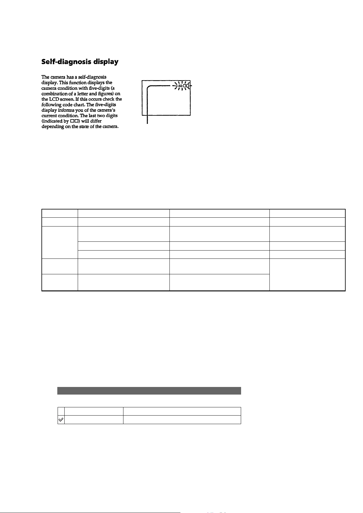
1-1. DESCRIPTION ON SELF-DIAGNOSIS DISPLAY
Self-diagnosis display
• C: ss: ss
You can reverse the camera
malfunction yourself. (However,
contact your Sony dealer or local
authorized Sony service facility
when you cannot recover from the
camera malfunction.)
• E: ss: ss
Contact your Sony dealer or local
authorized Sony service facility.
Display Code
C:32:ss
C:13:ss
E:61:ss
E:91:ss
Turn the power off and on again.
Format the “Memory Stick” or internal
memory.
Insert a new “Memory Stick”. “Memory Stick” is broken.
Turn the power off and on again. Trouble with internal memory.
Checking of lens drive circuit.
Checking of flash unit or replacement
of flash unit. (Note)
Countermeasure
Cause
Trouble with hardware.
“Memory Stick” or internal memory is
unformatted.
When failed in the focus and zoom
initialization.
Abnormality when flash is being
charged.
Caution Display During Error
SYSTEM ERROR
FORMAT ERROR
MEMORY STICK ERROR
INTERNAL MEMORY ERROR
—
Note: After repair, be sure to perfom “1-2. PROCESS AFTER FIXING FLASH ERROR”.
1-2. PROCESS AFTER FIXING FLASH ERROR
When “FLASH error” (Self-diagnosis Code E : 91 : ** ) occurs, to prevent any abnormal situation caused by high voltage, setting of the
flash is changed automatically to disabling charge and flash setting.
After fixing, this setting needs to be deactivated. Flash error code can be initialized by the operations on the Setup screen.
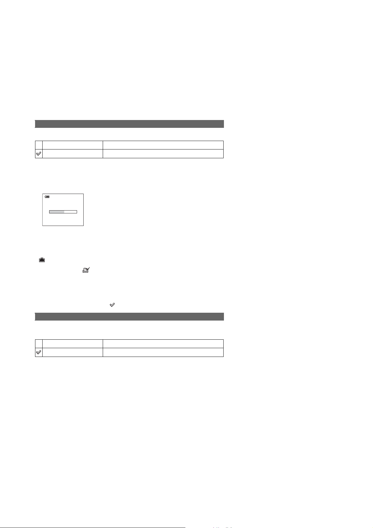
Method for Initializing the Flash Error Code
DSC-W50_L2
Initialize
Initializes the settin g to the default setting.
OK
Cancel
1 Select [OK] with v on the control button, then press z.
The message “Initialize all settings Ready?” appears.
2 Select [OK] with v, then press z.
The settings are reset to the default setting.
•Make sure that the power is not disconnected during resetting.
See the following procedure.
Cancels the resett in g .
1-1
1-3. METHOD FOR COPYING OR ERASING THE DATA IN INTERNAL MEMORY
The data can be copied/erased by the operations on the Setup screen. (When erasing the data, execute formatting the internal memory.)
Note 1: When replacing the SY-144 board, erase the data in internal memory of the board before replacement.
Note 2: When replacing the SY-144 board or the IC202 on the SY-144 board, execute formatting and initialize the internal memory after
replacement.
Method for Copying the Data in Internal Memory
Copy
Copies all images in the internal memory to a “Memory Stick Duo”.
OK
Cancel
1 Insert a “Memory Stick Duo” having 32 MB or larger capacity.
2 Select [OK] with v on the control button, then press z.
The message “All data in internal memory will be copied Ready?” appears.
3 Select [OK] with v, then press z.
Copying starts.
Copying
102_COPY
•Use a fully charged battery pack or the AC Adaptor (not supplied). If you attempt to copy image files
using a battery pack with little remaining charge, the battery pack may run out, causing copying to fail or
possibly corrupting the data.
•You cannot copy individual images.
•The original images in the internal memory are retained even after copying. To delete the contents of the
internal memory, remove the “Memory Stick Duo” after copying, then execute the [Format] command in
(Internal Memory Tool).
•You cannot select a folder copied on a “Memory Stick Duo”.
•Even if you copy data, a (Print order) mark is not copied.
See the following procedure .
Cancels the copying.
Method for Formatting the Internal Memory
This item does not appear when a “Memory Stick Duo” is inserted in the camera.
The default settings are marked with .
Format
Formats the internal memory.
•Note that formatting irrevocably erases all data in the internal memory, including even protected images.
OK
Cancel
1 Select [OK] with v on the control button, then press z.
The message “All data in internal memory will be erased Ready?” appears.
2 Select [OK] with v, then press z.
The format is complete.
See the following procedure .
Cancels the formatting.
DSC-W50_L2
1-2

1-4. PRECAUTION ON REPLACING THE SY-144 BOARD
VIDEO OUT Default Data Check
When you replace to the repairing board, the written data of repairing board also might be changed to original setting because of broadcast
system (NTSC/PAL).
When the data has changed because of board replacing etc., check the default data of VIDEO OUT if destination code is right. If not, rewrite
to the right value.
VIDEO OUT Default Data
Page
Writing Method:
1) Select page: 00, address: 01, and set data: 01.
2) Select page: 4F, address: 8D, and set data: 00 (NTSC) or data: 01 (PAL).
3) Select page: 40, address: 38, and set data: 00.
4) Click [Save] on the SEUS screen.
5) Select page: 80, address: 34, and check that the data is “00”.
6) Select page: 80, address: 30, and check that the data is “00”.
7) Select page: 00, address: 01, and set data: 00.
Address
NTSC PAL
Initial Language Data Check
Data
00 018D4F
If the SY-144 board was replaced, initial language setting may be changed. Accordingly, change the following data so as to set same initial
language as that of the set distributing in each region.
Initial language: Language displayed at the next starting if the setting of Setup menu was reset.
It is different from the language setting selectable with the menu.
Initial Language Data
Page Address Data Language GP2 GP3 GP4
00 English zzz
04 Spanish zz
4F 8C 08 Simplified Chinese z
0B Russian z
0D Korean z
Note: GP2 is fixed to English.
GP3 is either English, Spanish, or Russian.
GP4 is either English, Spanish, Simplified Chinese, or Korean.
Writing Method:
1) Select page: 00, address: 01 and set data: 01.
2) Select page: 4F, address: 8C, and set the Initial Language Data.
3) Select page: 40, address: 38, and set data: 00.
4) Click
5) Select page: 80, address: 34, and check that the data is “00”.
6) Select page: 80, address: 30, and check that the data is “00”.
7) Select page: 00, address: 01, and set data: 00.
8) Turn off the camera.
9) Turn on the camera. Execute “Initialize” of Setup screen.
10) Check the language displayed when the camera starts.
[Save] on the SEUS screen.
DSC-W50_L2
1-3E
NOTE FOR REPAIR
2. DISASSEMBLY
• Make sure that the flat cable and flexible board are not cracked of bent at the terminal.
Do not insert the cable insufficiently nor crookedly.
• When remove a connector, dont’ pull at wire of connector. It is possible that a wire is snapped.
• When installing a connector, dont’ press down at wire of connector.
It is possible that a wire is snapped.
• Do not apply excessive load to the gilded fle xible board.
Cut and remove the part of gilt
which comes off at the point.
(Be careful or some
pieces of gilt may be left inside)
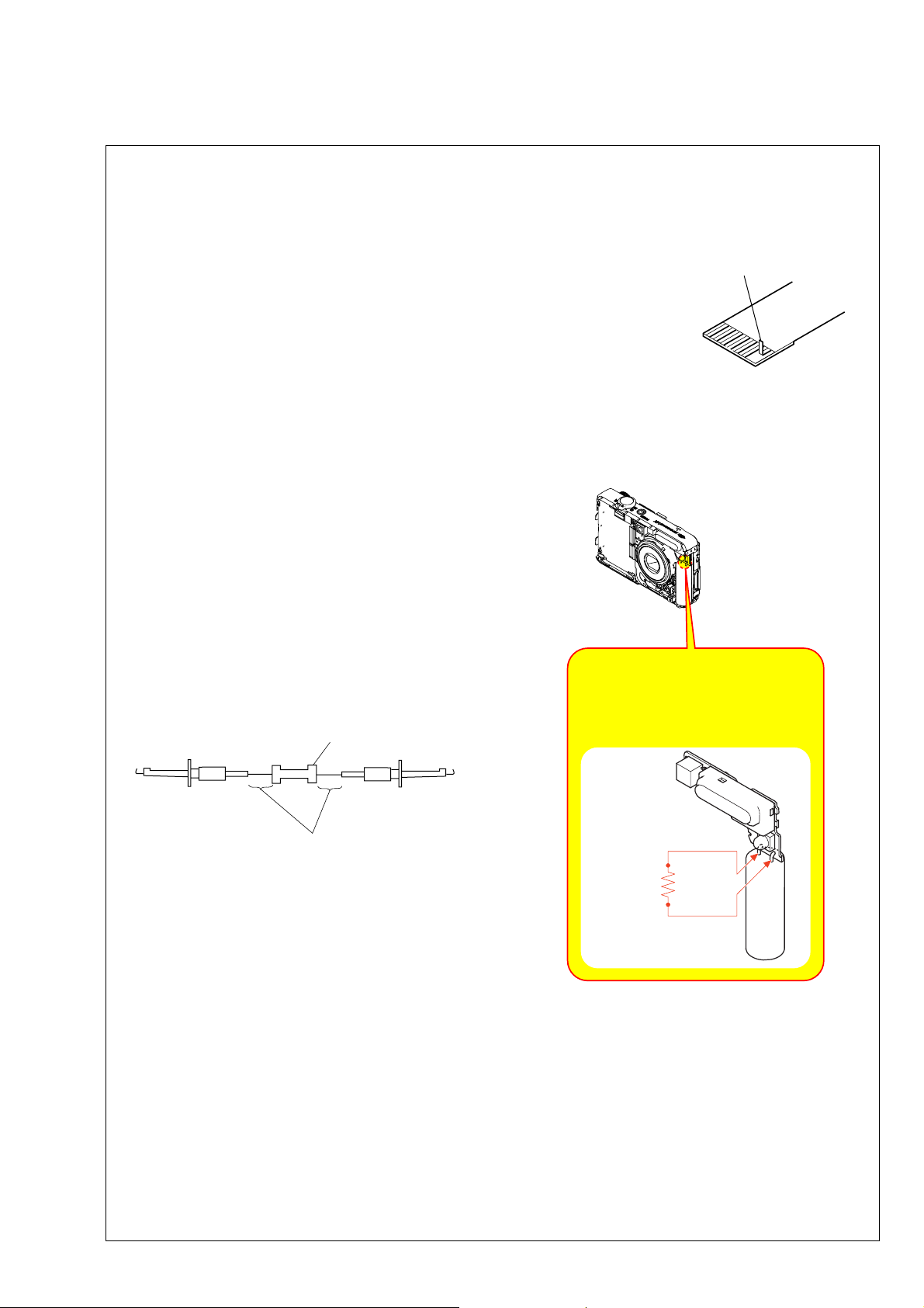
DISCHARGING OF THE ST-133 BOARD’S CHARGING CAPACIT OR (C901)
The charging capacitor (C901) of the ST-133 board is charged
up to the maximum 300 V potential.
There is a danger of electric shock by this high voltage when the
capacitor is handled by hand. The electric shock is caused by
the charged voltage which is kept without discharging when the
main power of the unit is simply turned off. Therefore, the
remaining voltage must be discharged as described below.
Preparing the Short Jig
To preparing the short jig, a small clip is attached to each end of
a resistor of 1 kΩ /1 W (1-215-869-11).
Wrap insulating tape fully around the leads of the resistor to
prevent electrical shock.
1 kΩ/1 W
Note: High-voltage cautions
Discharging the Capacitor
Short-circuit between the two points
with the short jig about 10 seconds.
DSC-W50_L2
Wrap insulating tape.
R:1 kΩ/1 W
(Part code: 1-215-869-11)
2-1
HELP
EXPLODED VIEW
HELP
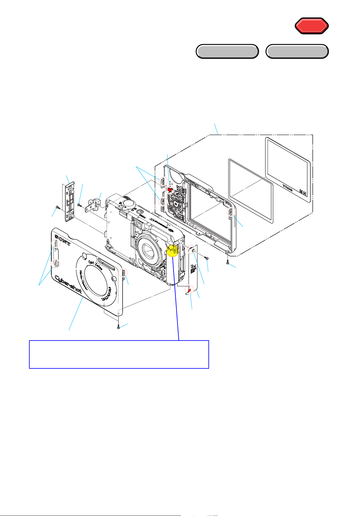
2-1. DISASSEMBLY
2-1-1. CABINET BLOCK
1-6
2-2 (#18)
1-5 (#18)
HARDWARE LIST
2 Cabinet (Rear) Block Assy
2-5 (Claw)
2-3 (Claw)
2-6
2-4 (Claw)
1-9 (Claw)1-8 (Claw)
1-3 (Claw)
1-7 (#18)
1 Cabinet (Front) Block Assy
Refer to page 2-1
" Discharging of the ST-133 board's charging capacitor (C901) ",
when discharging the capacitor.
2-1 (#18)
1-1 (#18)
1-2 (Claw)
1-4
DSC-W50_L2
2-2
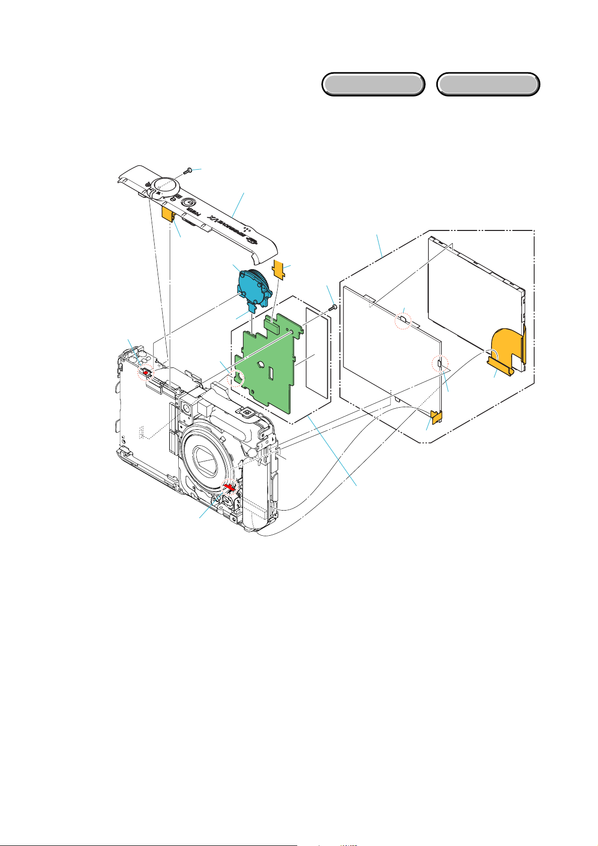
2-1-2. LCD BLOCK
EXPLODED VIEW
2-1 (Boss)
3-1 (#5)
3-2
2-3
2-2
2-5 (Claw)
HARDWARE LIST
3 Cabinet (Upper) Block Assy
1 LCD Block
2-6
2-4 (#5)
1-5
(Claw)
1-3 (Claw)
SW-464
1-2
1-4 (Claw)
1-1
2 SW-464 Board
DSC-W50_L2
2-3
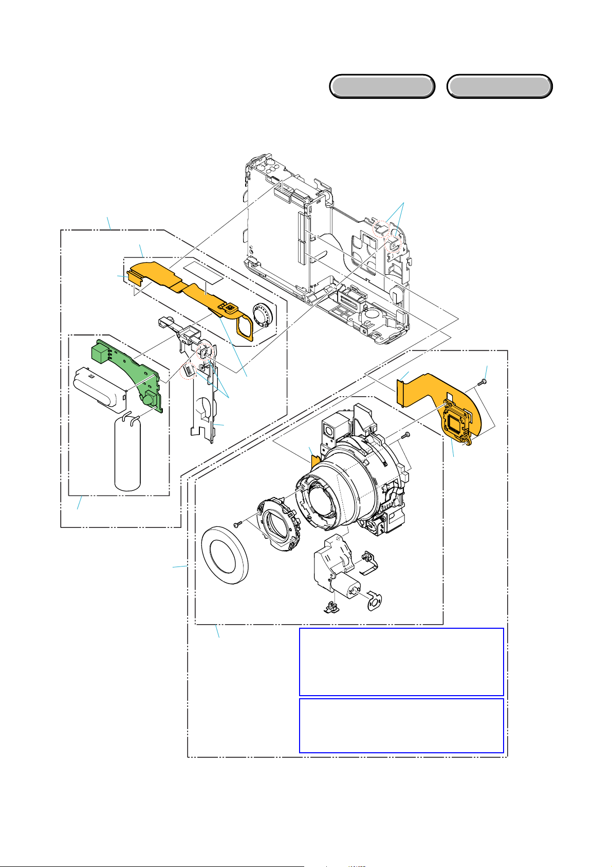
2-1-3. LENS BLOCK
EXPLODED VIEW
1-3
1-1
HARDWARE LIST
1-2 (Claw)
1-5
ST-134
ST-133
1 ST-133 Board
2-3
1-4
1-6 (Claw)
1-7
2 Lens Unit
2-1
2-2
Note 1:When you exchange barrier block
assembly and ornamental ring (A),
be sure to follow the procedure
carried on "2-2. Exchange Method
of Barrier Assembly" (2-6 page).
2-4 (#19)
CD-604
2-5
DSC-W50_L2
Note 2:When you exchange zoom motor
unit, be sure to follow the procedure
carried on "2-3. Exchange Method
of Zoom Motor Unit" (2-9 page).
2-4
2-1-4. BT HOLDER BLOCK
EXPLODED VIEW
3-6
HARDWARE LIST
3 DC-104 Flexible Board
3-1 (Claw)
3-5 (Claw)
DC-104
1 SW-144 Board
1-3
(Claw)
SY-144
1-1 (#5)
2-3 (#18)
1-5
1-4
2-1 (#18)
1-2
3-4
(Claw)
3-2
(Claw)
JK-303
2-2
2 JK-303 Flexible Board
2-4
HELP
3-3
DSC-W50_L2
2-5
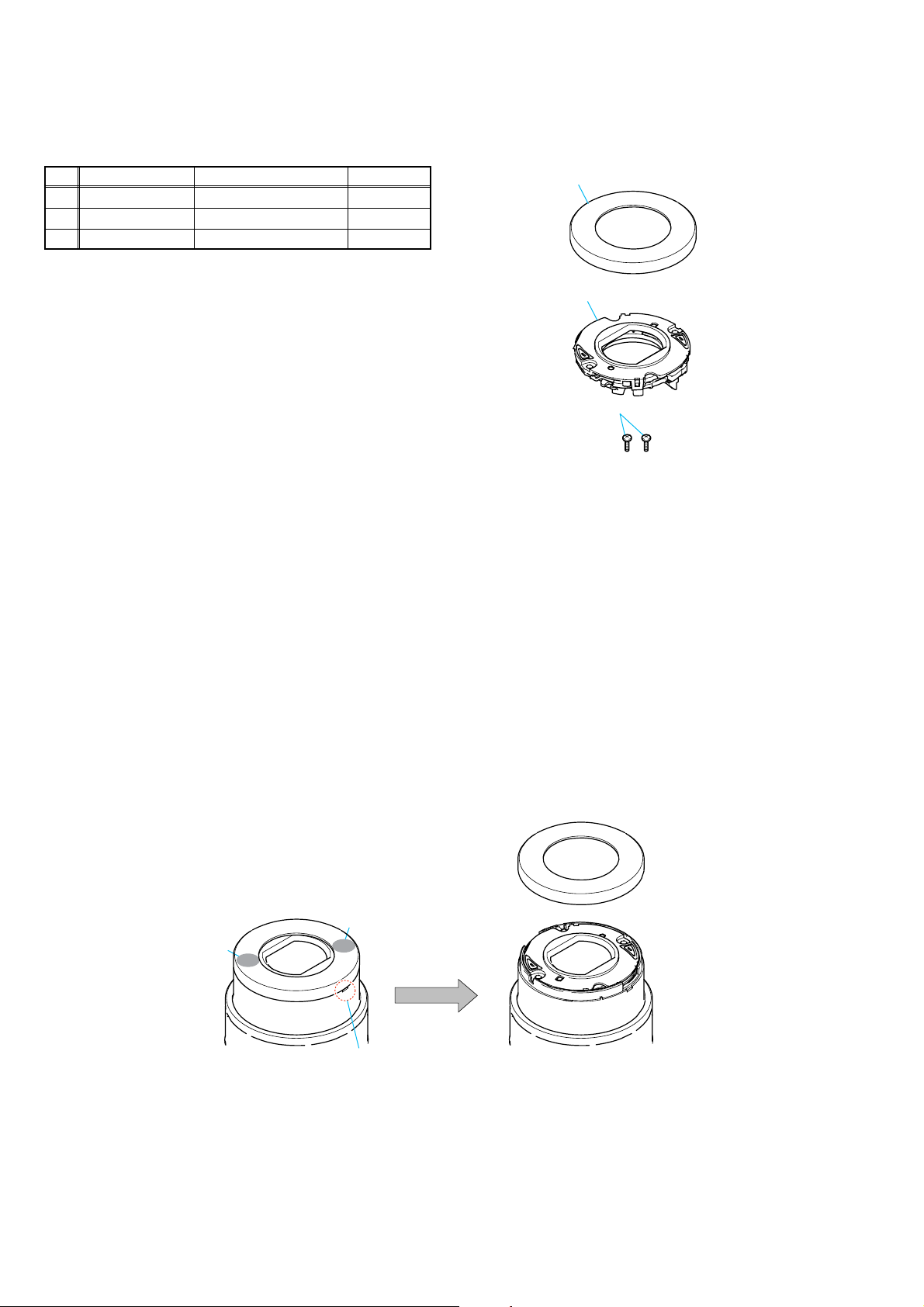
2-2. EXCHANGE METHOD OF BARRIER ASSY
Service parts
Part Number Part Name Quantity
1 2-673-650-01 Ring (A), Ornamental 1
2 2-673-652-01 Barrier Assy 1
3 2-673-651-01 Tapping screw (B1.2×4) 2
Tools used
Torque driver
Soldering iron
Weight about 60g
Adhesive tape (ornamental ring fixed) (2-677-885-01)
2-2-1. PEEL OFF OLD ORNAMENTAL RING A
The Ornamental Ring A has adhered to the Barrier Assy strongly and accordingly, use a soldering iron to weaken the adhesive force.
Heat four circled portions with the soldering iron.
Heating temperature is about 300ºC.
Beware of a burn since the entire Ornamental Ring becomes hot.
* As the adhesive force of Ornamental Ring A is considerably large, the forced peeling will damage the group-1 frame.
1
2
3
Insert the tip of tweezers, etc. into a notch of the group-1 frame and prize the ring.
* Take extreme care so as not to damage the coated surface of the group-1 frame.
In case of difficult peeling, heat the ring again with the soldering iron.
If this re-heating failed, it may be advisable that the ring be peeled while heating the portions 1 → 2 in the under figure one by one
sequentially.
* Discard the removed Ornamental Ring A.
1
2
Tip
DSC-W50_L2
2-6
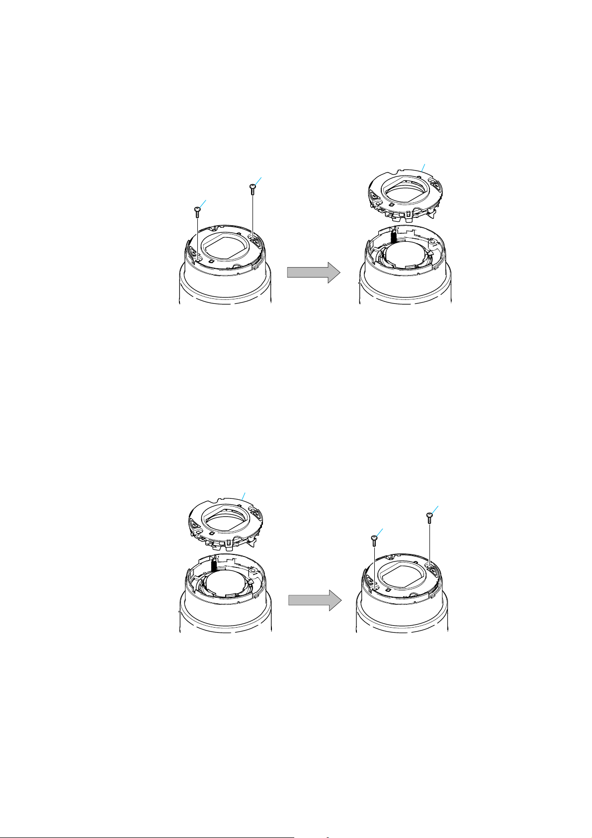
2-2-2. REMOVE OLD BARRIER ASSY
1 Remove two screws.
* Discard the removed screws.
2 Remove the Barrier Assy.
* Discard the removed Barrier Assy.
2
1
1
* After removing the Barrier Assy, if the “G1 Dust-Proof Ring” was removed, it must be returned to the home position.
In returning the ring, adjust the location of a projection to the lens direction.
This is an important part to prevent the dust and light from coming in.
* After removing the Barrier Assy, take extreme care not to drop dust or foreign substances in the lens barrel.
2-2-3. INSTALL NEW BARRIER ASSY
1 Install new Barrier Assy.
2 Tighten two screws.
* Tightening torque = 0.5 kgf
1
2
2
DSC-W50_L2
2-7
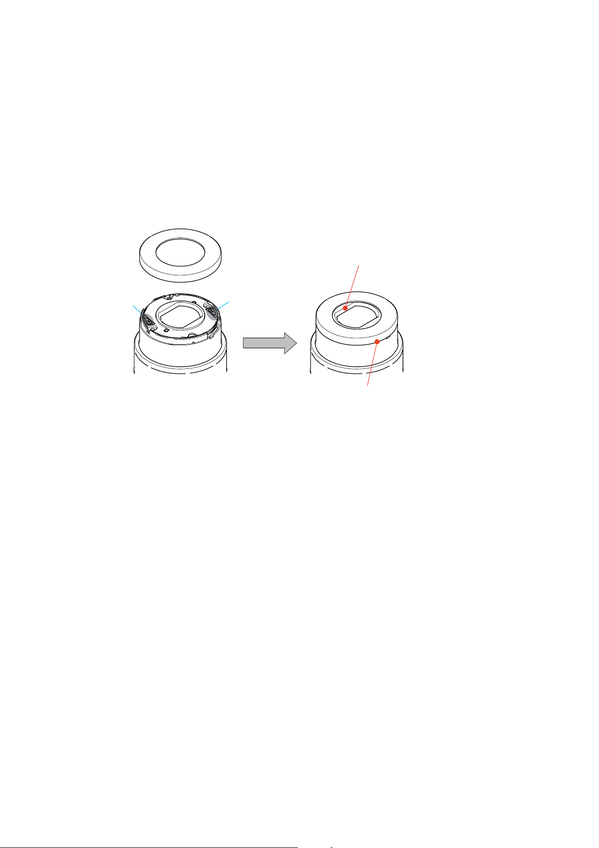
2-2-4. ADHERE THE ORNAMENTAL RING A
Apply an adhesive tape to two recesses on the top surface of the Barrier Assy.
Meeting a “notch” of the Ornamental Ring A with a “projection” of the group-1 frame, push the Ornamental Ring A into the group-1 frame.
* The projection of the spring for preventing static electricity must be tilted.
Put the 60g weight on the Ornamental Ring A so that the Ornamental Ring A does not float up until the adhesive hardens.
Note: Be careful not to give a shock.
* After the weight was put, no gap must be present in full circumference between Ornamental Ring A and group-1 frame.
A gap, if present, causes the crackle sound NG.
* The weight must push in the Ornamental Ring A only.
If the weight is put on the mold part of the Barrier Assy, the Ornamental Ring A will float up.
Do not put the weight on a black mold part.
Adhesive
tape
Completion after 30 minutes.
Adhesive
tape
Not gap in full circumference.
DSC-W50_L2
2-8
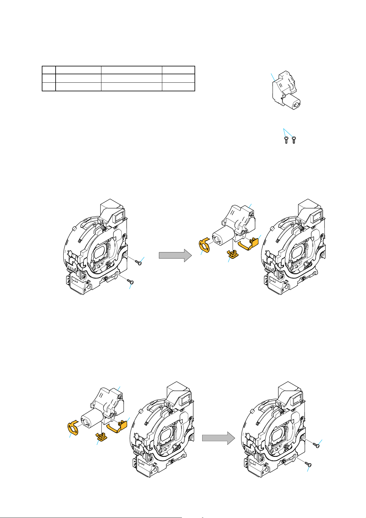
2-3. EXCHANGE METHOD OF ZOOM MOTOR UNIT
Service parts
Part Number Part Name Quantity
1 2-673-648-01 Zoom Motor Unit 1
2 2-673-649-01 BT2 P1.4×3 B3C 2
Tools used
Torque driver
1
2-3-1. REMOVE OLD ZOOM MOTOR UNIT
1 Remove two screws.
* Discard the removed screws.
2 Remove the Zoom Motor Unit.
3 Remove the Lens Flexible Board.
* Discard the removed Zoom Motor Unit.
1
1
2
2
3
3
3
2-3-2. INSTALL NEW ZOOM MOTOR UNIT
1 Install the Lens Flexible Board in new Zoom Motor Unit.
2 Install new Zoom Motor Unit in the Lens Block.
3 Tighten two screws.
* Tightening torque = 0.7 kgf
DSC-W50_L2
1
2
1
3
1
3
2-9E
HELP
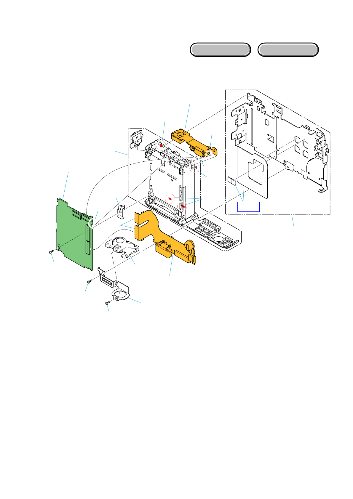
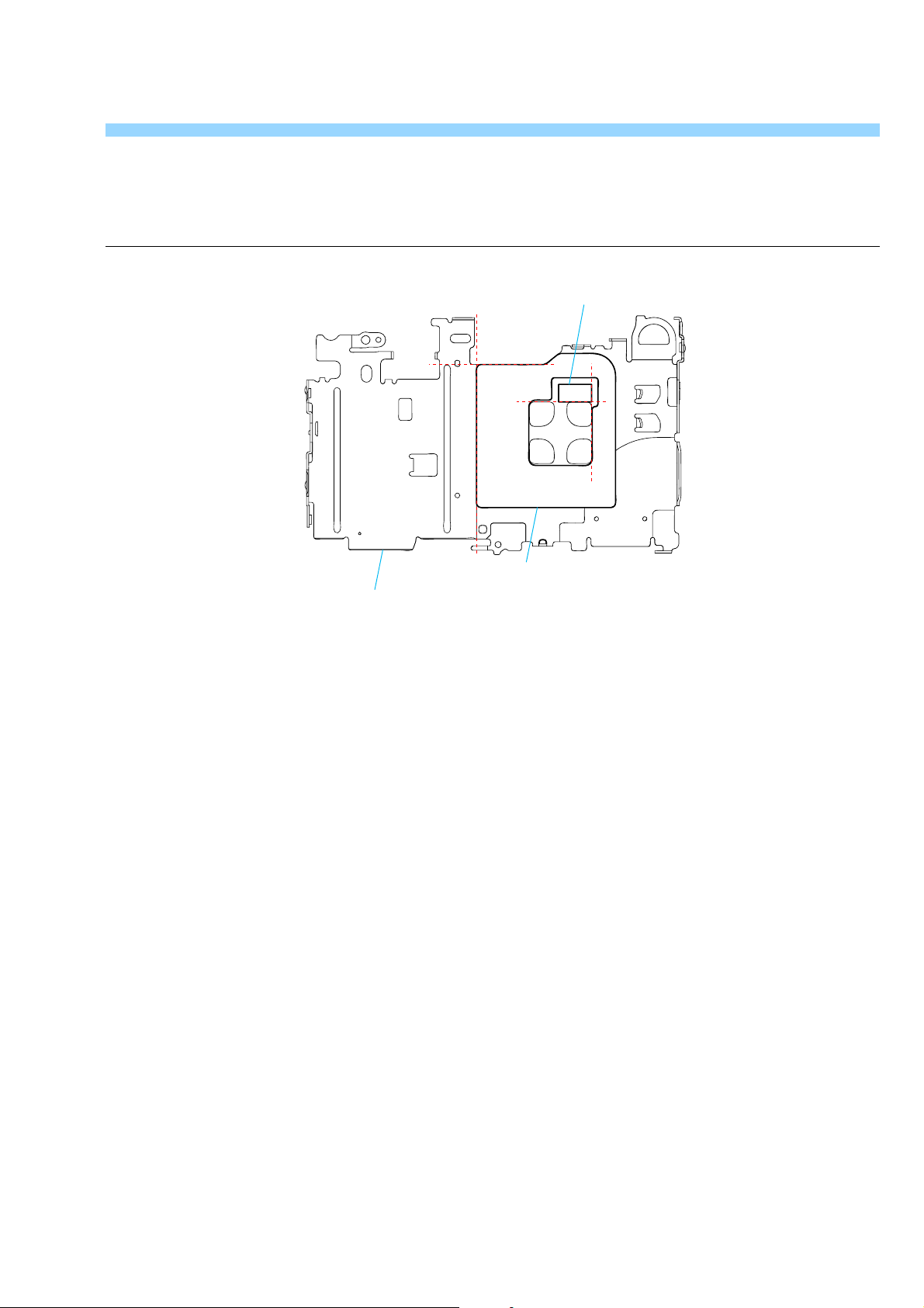
Sheet attachment positions and procedures of processing the flexible boards/harnesses are shown.
CD radiation cushion
Lens cushion (130)
LCD frame (130)
DSC-W50_L2
HELP

3. BLOCK DIAGRAMS
Link
Link
OVERALL BLOCK DIAGRAM (1/2) POWER BLOCK DIAGRAM
OVERALL BLOCK DIAGRAM (2/2)
DSC-W50_L2
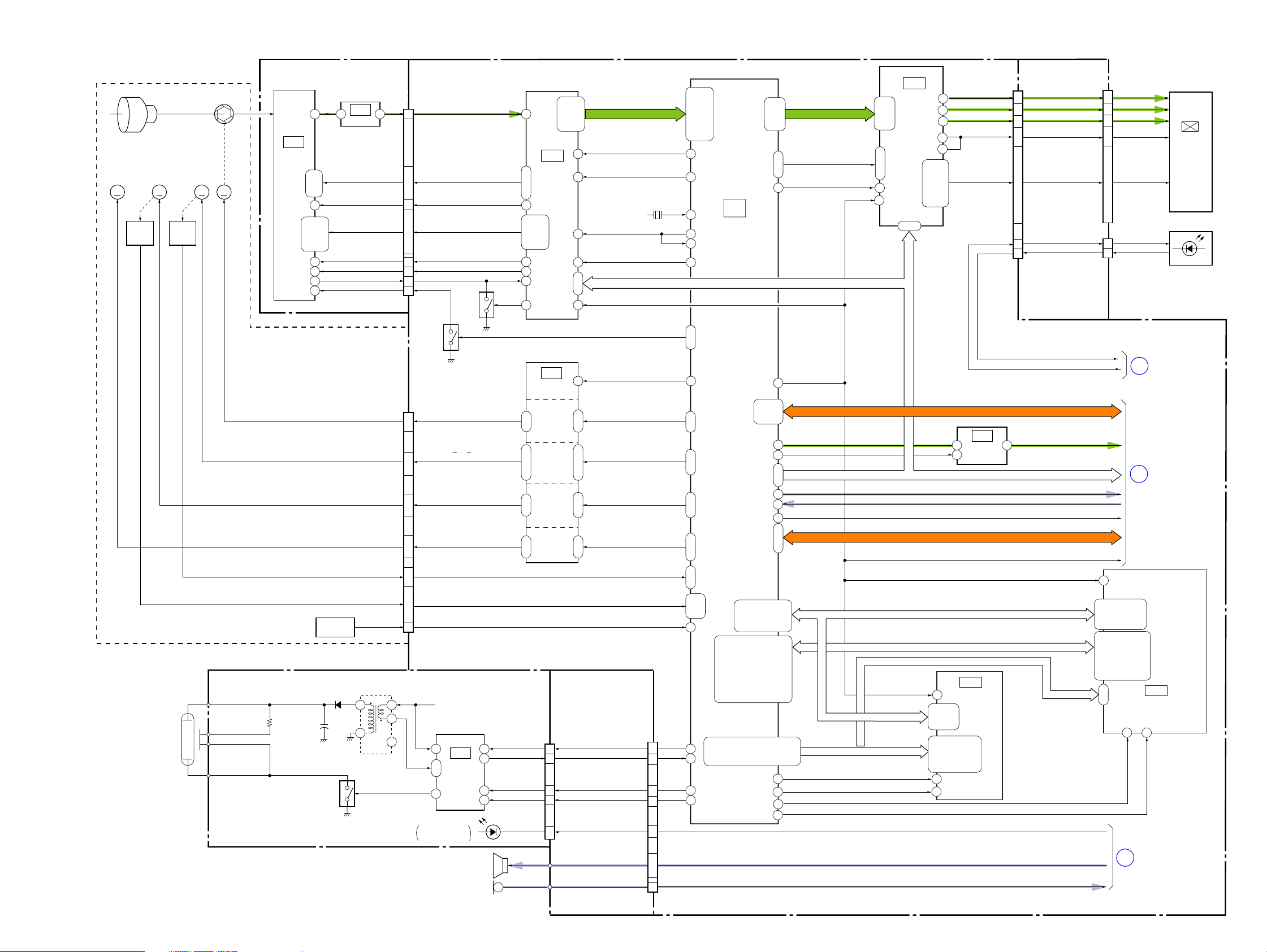
3. BLOCK DIAGRAMS
3-1. OVERALL BLOCK DIAGRAM (1/2)
LENS BLOCK
LENS
SHUTTER
MOTOR
M
ZOOM
SENSOR
1, 2
ZOOM
MOTOR
M
FLASH
UNIT
FOCUS
RESET
SENSOR
FOCUS
MOTOR
M
05
A : VIDEO SIGNAL
A : AUDIO SIGNAL
A : VIDEO/AUDIO SIGNAL
IRIS
(METER)
IRIS
MOTOR
M
ST-133 BOARD
XE_H
TRIGGER
TRIGGER_GND
XE_L
CD-604 FLEXIBLE BOARD
17 31
IC002
CCD
IMAGER
31, 32
21, 22,
19
1 - 3, 5, 6
8 - 10, 12
11
7
26 C4
27
Z_BOX2_PI_SENS_COL, Z_BOX1_PI_SENS_COL,
XZM_RST_LED, Z_BOX1, BOX2,
LENS TEMP
SENSOR
C901
+
CHARGING
CAPACITOR
Q001
FLASH
DRIVE
( ) : Number in parenthesis ( ) indicates the division number of schematic diagram where the component is located.
SY-144 BOARD (1/2)
1
2
CN301
16
2 - 4, 6
8
23 - 29, 31 - 35
22
30
39
38
CN401
20, 21
12 - 158 - 1116 - 19
24, 26
2, 3, 5, 6, 27. 29
30
CCD_OUT
H1A, H2A, H1B, H2B
RG
V1A,V1B,V2,V3A,V3B,V4
V5A,V5B,V6,V7A,V7B,V8
VHLD
VST
VSUB
VSUB_CONT
Q301
Q302
IRIS_ M_+, M_–
FOCUS_A, A, B, B
ZOOM_DC_+, DC_–
SHUTTER_+, –
ST_UNREG
15
IC001
FLASH
1, 2
CONTROL,
CHARGE
CONTROL
7
D003
SELF-TIMER/
AF ILLUMINATOR
SP901
SPEAKER
MIC901
H10
IC301
CCD SIGNAL
PROCESS,
TIMING
GENERATOR
K6, K5, J6, J5
(1/7)
K4
E4, D7, H7, D4
H5, H4, G4, F4,
G7, H6, G6, G5,
D5
D6
E7
IC401
LENS DRIVE
(3/7)
IRIS MOTOR
DRIVER
D2, B1
FOCUS
MOTOR
DRIVER
D6, E6, B7, C6
ZOOM
MOTOR
B4, B5F4, F3
DRIVER
SHUTTER
MOTOR
DRIVER
FC_SENS, XFC_RST_LED
ZM_DC_FG_1A, ZM_DC_FG_1B,
XZM_FG_LED, ZM_SENS_1ST,XZM_RST_LED
LENS_TEMP
H1 - H3, J1
D1, E1 - E3,
F1 - F3, G1 - G3,
A2
A3
A4
C2
B3, C3
C1
D4
D3, E3
D5, A6, B6, C5
B2, C4, A2
G1, E4
ST-134 FLEXIBLE BOARD
10
CN001
9
4
6
STRB_CHG
9
XSTRB_FULL
12
STRB_ON
10 15
STRB_CHG_CONT
11
XAF_LED
14
SP+, SP-
MIC_SIG
CA_AD00 – CA_AD13
CA_HD
CA_FD
X102
33.75MHz
CLKTGO
XCS_FE
IC_101_1_SO, XIC_101_1_SCK
XIC_101_RST_OUT
VSUB_CONT_PRE,
VSUB_CONT_POST
XCAM_DR_PS
IRIS_M_IN, IRIS_M_EN
FC_DIR_A,
FC_DIR_B,
FC_BRK_A
ZM_DIR_A,
ZM_BRK_A,
ZM_BRK_B
MSHUT_DIR,
MSHUT_EN
CN704
14
17
16
19
22, 23
21
B21, A21
B4, D5 - D8,
W25
AF4
AE4, AE5,
AB6, AC4,
H26
U23
K26
L26
Y26
AE6
AF9
A17
A18
K4,M6,K1, K2
H2, J1, J2, M5, J4,
K5, G4, H4, L5, H1,
H5
J5
IC101
C1
E1
F2
U22
T4, R23
P21
P4, N4
N5, L2, L4
P5, N2, N6
R5, R25U4, E5
J25
R22
V23
R4
AB22
(1/2)
CAMERA DSP, CPU,
LENS CONTROL,
MODE CONTROL
(2/7)
V5, W4
B3, D4, V4,
AB13, AA13, AE13, AF13,
AF12, AE12, AA12, AC12,
AC11, AB12, AE11, AF11,
AE10, AB11, AC10, AB10
D21, D22, D20, B22, A22, A23,
B23, E20, E21, B24, A24, A25,
B25, C25, C26, B26, E10, A10,
D10, E11, B10, A11, B11, E12,
D11, D12, F12, B12, A12, E13,
D13, D14, F13, B15, F14, E14,
D17, D18, D16, B18, A19, B19,
E16, D19, E19, E17, B20, A20,
AF21, AF20, AE20, AB18, AB19, AC19,AB16,
AE19, AF19, AF18, AE18, AA15, AC18, AC17,
AB15, AE17, AF17, AE16, AB14, AC16, AC15
LCD_D0 - LCD_D7
E6 - E8
LCD_HD, LCD_VD,LCD_CK
B8, D9, E9
XIC_101_RST_OUT
AC5,AF6
IC_101_VOUT
VIDEO_AMP_ON
IC_101_1_SO, XIC_101_1_SCK
R6, U2
AC1, AD1
XCPU_CS0
IC_101_27M_CLKO
DSP_QCLKE
DSP_QCLK
IC001
BUFFER
14 - 16
IRIS_ (+), (–)
F_MOTOR_A, A(–), B, B(–)
Z_DC_MOTOR (+), (–)
SHUTTER_(+), (–)
F_PI_SENS_OUT,
XFC_RST_LED
Z_PI_SENS_OUT
D002
T001
5 4
3
IC901
LCD DRIVE
(5/7)
B3 - B7
A3, A5, A7
XCS_ PANEL
XIC_101_RST_OUT
XIC_101_RST_OUT
DSP_AQ0 – DSP_AQ11, DSP_DQ0 – DSP_DQ31,
CPU_D00- CPU_ D15
CPU_A01- CPU_A21
A2, A9, C9
B10
C10
A10, B9
IC_101_1_SO, XIC_101_1_SCK
MS_BS, MS_D0 – MS_D3, MS_CLK
XIC_101_RST_OUT
CPU_D00- CPU_ D15
CN901
K2
K3
K1
K6
J6
RGT, PSIG,
HCK1, HCK2, REF,
HST, PCG, XSTBY,
DWN, EN, VCK, VST
J4, D1, E2, F2,
F1, G2, G1, H2
B1, K4, C2, D2,
VIDEO AMP
4
USB_DP, USB_DM
XIC_101_RST_OUT
CPU_D00 – CPU_D15
DSP_DQM0 – DSP_DQM3, DSP_QBA0, DSP_QBA1
CPU_A20, CPU_A21
IC201
BURST
B5
FLASH
(4/7)
E2 - E6, D5,
F2 - F7, G1,
G3, G5, G7
A1, A2, A6, A7, A8, B1,
B2, B3, B6, B7, B8, C1,
C2, C6, C7, C8, D1, D2,
D4, D8, E8
E7
B4
R
GG
B
CS, COM
IC602
53
(6/7)
JK-303 FLEXIBLE
BOARD(1/2)
8
9
7
CS, COM
27, 286, 10 - 12, 15 - 18, 23 - 26
RGT, PSIG,
HCK1, HCK2, REF,
HST, PCG, XSTBY,
DWN, EN, VCK, VST
1
3
IC_101_1_SO, XIC_101_1_SCK
XIC_101_RST_OUT
R
B
BL_H
BL_L
V_LINE_OUT
IC_101_AUOUT
IC_101_AUIN
XCS_AUDIO
DSP_QCLKE
DSP_QCLK
XAF_LED
SP+, SP-
MIC_SIG
CN102
CN101
21
20
22
1, 23 - 6, 11 - 14, 17 - 19, 23
6
1
BL_L
BL_H
B4
C9, C10, D9, D10, D11,
D12,E10, E11, J10, J11,
J12, K10,K11, K12, L11,
L12
C5 - C8, D5 - D8, E4, E5,
E8, E9, F3 - F9, G2 - G5,
G9, G10, H2, H3, H4, H8,
H9, H10, J3 - J9, K3, K4,
K8, K9, L4, L5, L9, L10,
M4, M5, M9, M10
M3, E3
1
2
IC202
128M SDRAM,
32M SUPER AND
M7
N7
OVERALL (2/2)
3
(PAGE 3-2)
OVERALL (2/2)
(PAGE 3-2)
OVERALL (2/2)
(PAGE 3-2)
(4/7)
LCD901
2.5 INCH
COLOR
LCD
MONITOR
D901
BACKLIGHT
DSC-W50_L2
3-1
 Loading...