

SONY DSC-T20, DSC- T25 L3 Service Manual V1.0
DSC-T20/T25
SERVICE MANUAL
Ver 1.0 2007.03
Revision History
Revision History
How to use
How to use
Acrobat Reader
Acrobat Reader
Internal memory
Internal memory
ON BOARD
ON BOARD
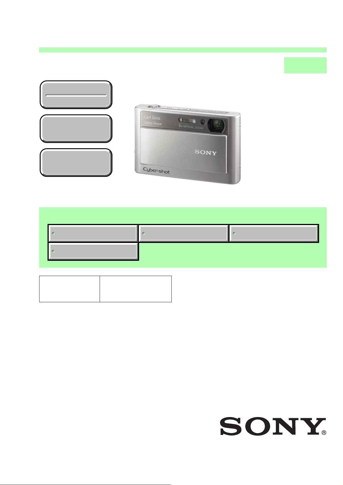
Photo: Silver
Link
Link
SERVICE NOTE
PRINTED WIRING BOARDS
LEVEL 3
US Model
Canadian Model
AEP Model
UK Model
E Model
Australian Model
Hong Kong Model
Chinese Model
Korea Model
Argentine Model
Brazillian Model
Japanese Model
Tourist Model
REPAIR PARTS LIST
SCHEMATIC DIAGRAMS
The components identified by
mark 0 or dotted line with
mark 0 are critical for safety.
Replace only with part number specified.
Les composants identifiés par une
marque 0 sont critiques pour la
sécurité.
Ne les remplacer que par une pièce
portant le numéro spécifié.
DIGITAL STILL CAMERA
DSC-T20/T25_L3
Sony EMCS Co.
2007C0800-1
© 2007.03
Published by Kohda TEC9-852-195-11
Model information table
Model
Destination
• Abbreviation
AR : Argentine model
AUS: Australian model
BR : Brazilian model
CH : Chinese model
CND: Canadian model
EE : East European model
HK : Hong Kong model
J : Japanese model
JE : Tourist model
KR : Korea model
NE : North European model
TW : Taiwan model
US, CND, AEP, UK, E, AUS,
HK, CH, KR, AR, BR, J, JE
DSC-T20
DSC-T25
AEP, E, AUS, HK
Danger of explosion if battery is incorrectly replaced.
CAUTION
Replace only with the same or equivalent type.
SAFETY-RELATED COMPONENT WARNING!!
COMPONENTS IDENTIFIED BY MARK 0 OR DOTTED LINE WITH
MARK 0 ON THE SCHEMATIC DIAGRAMS AND IN THE PARTS
LIST ARE CRITICAL TO SAFE OPERATION. REPLACE THESE
COMPONENTS WITH SONY PARTS WHOSE PART NUMBERS
APPEAR AS SHOWN IN THIS MANUAL OR IN SUPPLEMENTS
PUBLISHED BY SONY.
SAFETY CHECK-OUT
After correcting the original service problem, perform the following
safety checks before releasing the set to the customer.
1. Check the area of your repair for unsoldered or poorly-soldered
connections. Check the entire board surface for solder splashes
and bridges.
2. Check the interboard wiring to ensure that no wires are
"pinched" or contact high-wattage resistors.
3. Look for unauthorized replacement parts, particularly
transistors, that were installed during a previous repair. Point
them out to the customer and recommend their replacement.
4. Look for parts which, through functioning, show obvious signs
of deterioration. Point them out to the customer and
recommend their replacement.
5. Check the B+ voltage to see it is at the values specified.
6. FLEXIBLE Circuit Board Repairing
• Keep the temperature of the soldering iron around 270°C
during repairing.
• Do not touch the soldering iron on the same conductor of the
circuit board (within 3 times).
• Be careful not to apply force on the conductor when soldering
or unsoldering.
ATTENTION AU COMPOSANT AYANT RAPPORT
À LA SÉCURITÉ!
LES COMPOSANTS IDENTIFÉS PAR UNE MARQUE 0 SUR LES
DIAGRAMMES SCHÉMATIQUES ET LA LISTE DES PIÈCES SONT
CRITIQUES POUR LA SÉCURITÉ DE FONCTIONNEMENT. NE
REMPLACER CES COMPOSANTS QUE PAR DES PIÈSES SONY
DONT LES NUMÉROS SONT DONNÉS DANS CE MANUEL OU
DANS LES SUPPÉMENTS PUBLIÉS PAR SONY.
Unleaded solder
Boards requiring use of unleaded solder are printed with the leadfree mark (LF) indicating the solder contains no lead.
(Caution: Some printed circuit boards may not come printed with
the lead free mark due to their particular size.)
: LEAD FREE MARK
Unleaded solder has the following characteristics.
• Unleaded solder melts at a temperature about 40°C higher than
ordinary solder.
Ordinary soldering irons can be used but the iron tip has to be
applied to the solder joint for a slightly longer time.
Soldering irons using a temperature regulator should be set to
about 350°C.
Caution: The printed pattern (copper foil) may peel away if the
heated tip is applied for too long, so be careful!
• Strong viscosity
Unleaded solder is more viscous (sticky, less prone to flow) than
ordinary solder so use caution not to let solder bridges occur such
as on IC pins, etc.
• Usable with ordinary solder
It is best to use only unleaded solder but unleaded solder may
also be added to ordinary solder.
DSC-T20/T25_L3
— 2 —

TABLE OF CONTENTS
Section Title Page
1. SERVICE NOTE
1-3. Method for Copying or Erasing the Data in Internal
Memory (Internal Memory/Music) ································· 1-2
4. PRINTED WIRING BOARDS AND
SCHEMATIC DIAGRAMS
4-2. Schematic Diagrams ························································4-2
4-3. Printed Wiring Boards ··················································· 4-16
4-4. Mounted Parts Location ················································ 4-22
5. REPAIR PARTS LIST
5-2. Electrical Parts List ························································· 5-6
DSC-T20/T25_L3
— 3 —

1. SERVICE NOTE
1-4. METHOD FOR COPYING OR ERASING THE DATA IN INTERNAL MEMORY
(INTERNAL MEMORY/MUSIC)
The data can be copied/erased by the operations on the Setup screen. (When erasing the data, execute formatting the internal memory.)
Note 1: When replacing the SY-170 board, erase the data in internal memory of the board before replacement.
Note 2: When replacing the SY-170 board execute formatting and initialize the internal memory after replacement.
Method for Copying the Data in Internal Memory
Copy
Copies all images in the internal memory to a “Memory Stick Duo”.
1 Insert a “Memory Stick Duo” having 32 MB or larger capacity.
2 Select [Copy] with v/V/b/B on the control button, then press z.
The message “All data in internal memory will be copied” appears.
3 Select [OK] with v, then press z.
Copying starts.
To cancel the copying
Select [Cancel] in step 3, then press z.
•Use a fully charged battery pack. If you attempt to copy image files using a battery pack with little
remaining charge, the battery pack may run out, causing copying to fail or possibly corrupting the data.
•You cannot copy individual images.
•The original images in the internal memory are retained even after copying. To delete the contents of the
internal memory, remove the “Memory Stick Duo” after copying, then execute the [Format] command in
[ Internal Memory Tool ] .
•When you copy the data in the internal memory to the “Memory Stick Duo”, all the data will be copied.
Yo u cannot choose a specific folder on the “Memory Stick Duo” as the destination for the data to be
copied.
•Even if you copy data, a DPOF (Print order) mark is not copied.
Method for Formatting the Internal Memory
This item does not appear when a “Memory Stick Duo” is inserted in the camera.
Format
Formats the internal memory.
•Note that formatting irrevocably erases all data in the internal memory, including even protected images.
1 Select [OK] with v on the control button, then press z.
The message “All data in internal memory will be erased Ready?” appears.
2 Select [OK] with v, then press z.
The format is complete.
To canc el the formatting
Select [Cancel] in step 1 or 2, then press z.
Method for Formatting the Music
Format Music
If you cannot play back a Music file for the Slide Show, the Music file might be corrupted. If
this happens, perform [Format Music].
When [Format Music] is performed, all the Music files are erased. Use the supplied software
“Music Transfer” to activate [Download Music].
1 Select [OK] with v on the control button, then press z.
The message “All data will be erased Ready?” appears.
2 Select [OK] with v, then press z.
All the Music files are erased.
To canc el the formatting
Select [Cancel] in step 1 or 2, then press z.
DSC-T20/T25_L3
1-3

Link
Link
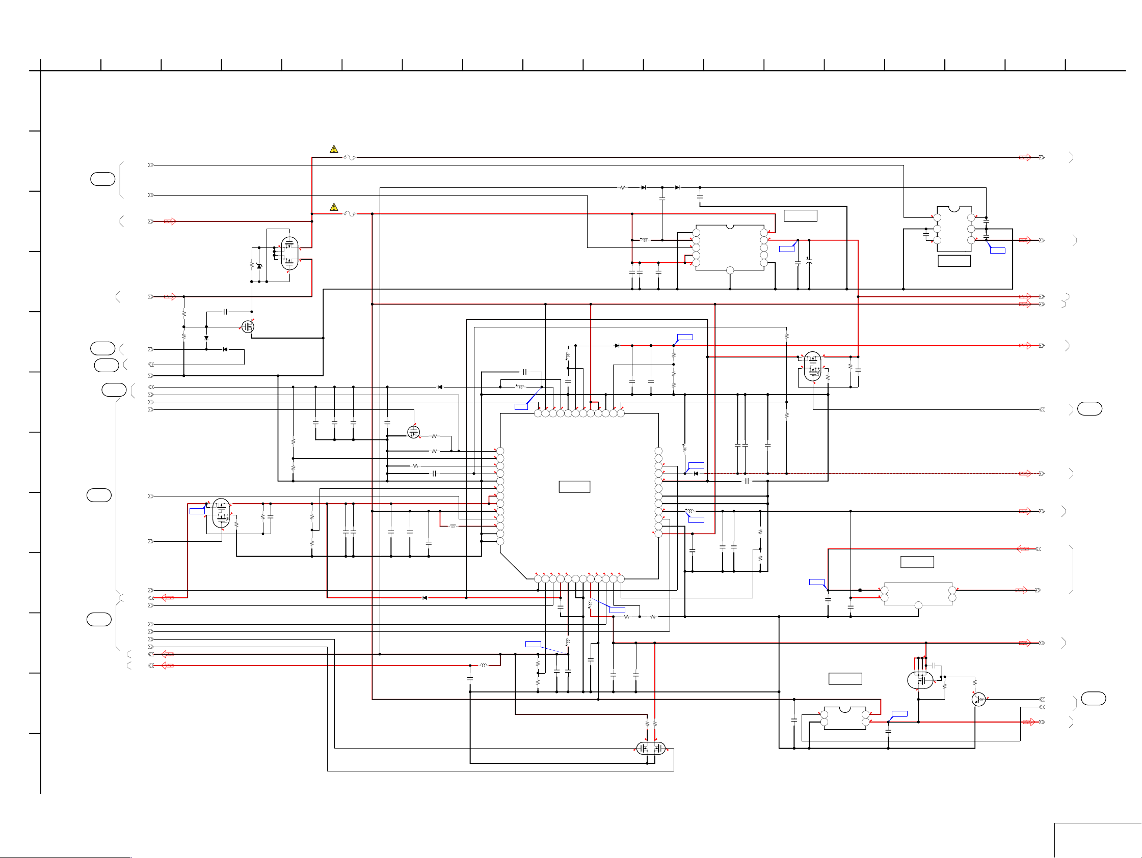
4-2. SCHEMATIC DIAGRAMS
SY-170 BOARD (1/8) (DC/DC CONVERTER)
SY-170 BOARD (2/8)
(POWER/ENABLE SIG CONTROLLER)
SY-170 BOARD (3/8)
(CAMERA DSP, MODE CONTROL)
SY-170 BOARD (4/8)
(CAMERA DSP, LENS CONTROL, FRONT CONTROL)
COMMON NOTE FOR SCHEMATIC DIAGRAMS
SY-170 BOARD (5/8)
SY-170 BOARD (6/8) (LENS DRIVER)
SY-170 BOARD (7/8)
SY-170 BOARD (8/8) (AUDIO, VIDEO AMP)
(CCD SIGNAL PROCESS)
(LENS DRIVE, OIS DRIVE)
DSC-T20/T25_L3

4-2. SCHEMATIC DIAGRAMS
4-2. SCHEMATIC DIAGRAMS
4. PRINTED WIRING BOARDS AND SCHEMATIC DIAGRAMS
4-2. SCHEMATIC DIAGRAMS
THIS NOTE IS COMMON FOR SCHEMATIC DIAGRAMS
(In addition to this, the necessary note is printed in each block)
(For schematic diagrams)
• All capacitors are in µF unless otherwise noted. pF : µ
µF. 50 V or less are not indicated except for electrolytics
and tantalums.
• Chip resistors are 1/10 W unless otherwise noted.
kΩ=1000 Ω, MΩ=1000 kΩ.
• Caution when replacing chip parts.
New parts must be attached after removal of chip.
Be careful not to heat the minus side of tantalum
capacitor, Because it is damaged by the heat.
• Some chip part will be indicated as follows.
Example C541 L452
22U 10UH
TA A 2520
Kinds of capacitor
External dimensions (mm)
Case size
• Constants of resistors, capacitors, ICs and etc with XX
indicate that they are not used.
In such cases, the unused circuits may be indicated.
• Parts with ★ differ according to the model/destination.
Refer to the mount table for each function.
• All variable and adjustable resistors have characteristic
curve B, unless otherwise noted.
• Signal name
XEDIT → EDIT PB/XREC → PB/REC
• 2: non flammable resistor
• 5: fusible resistor
• C: panel designation
• A: B+ Line
• B: B– Line
• J : IN/OUT direction of (+,–) B LINE.
• C: adjustment for repair.
• A: not use circuit
(Measuring conditions voltage and waveform)
• Voltages and waveforms are measured between the
measurement points and ground when camera shoots
color bar chart of pattern box. They are reference values
and reference waveforms.
(VOM of DC 10 MΩ input impedance is used)
• Voltage values change depending upon input
impedance of VOM used.)
1. Connection
Pattern box
Pattern box PTB-450
J-6082-200-A
or
Small pattern box
PTB-1450
J-6082-557-A
L = 24 cm (PTB-450)
L = 11 cm (PTB-1450)
Pattern box
Color bar chart
L
For PTB-450:
J-6020-250-A
For PTB-1450:
J-6082-559-A
Front of the lens
Camera
2. Adjust the distance so that the output waveform of
Fig. a and the Fig. b can be obtain.
H
Yellow
Cyan
White
Magenta
Green
AABBA=B
Fig. a (Video output terminal output waveform)
Fig.b (Picture on monitor TV)
Red
Blue
Electronic beam
scanning frame
CRT picture frame
Precautions for Replacement of Imager
• If the imager has been replaced, carry out all the adjustments
for the camera section.
• As the imager may be damaged by static electricity from
its structure, handle it carefully like for the MOS IC.
In addition, ensure that the receiver is not covered with
dusts nor exposed to strong light.
DSC-T20/T25_L3
When indicating parts by reference number, please
include the board name.
The components identified by mark 0 or dotted line with
mark 0 are critical for safety.
Replace only with part number specified.
Les composants identifiés par une marque 0 sont
critiques pour la sécurité.
Ne les remplacer que par une pièce portant le numéro
spécifie.
4-2
• Refer to page 4-3 for mark 0.
1
SY-170 BOARD(1/8)
A
DC/DC CONVERTER
XX MARK:NO MOUNT
NO MARK:REC/PB MODE
B
2
PANEL_EN
@001
(2/8)
C
(8/8)
EVER_PSB
ACV_UNREG
D
BATT_UNREG
(8/8)
E
F
(8/8)
(3/8)
@002
(4/8)
@003
@004
XACV_DET
XACV_IN
REG_GND
BL_H
BL_L
BL_EN1
BL_EN2
G
@005
(2/8)
VSU_EN
H
DDC5PSW_EN
I
(3/8) (6/8)
(7/8) (8/8)
@006
(2/8)
J
(2/8) (3/8) (4/8) (5/8)
(6/8) (7/8) (8/8)
(4/8) (7/8) (8/8)
CAMDD_EN
MAX_5.0V
DDC2P9_EN
DDC1P8_EN
DDC1P2_EN
DISW2P9_EN
DISW1P8_EN
D_3.0V
A_3.0V
K
L
R002
470k
R003
3
1M
5.0V
5.0
0.6
C004
1u
D002
MA2SD32008S0
D003
MA2SD32008S0
Q003
SSM6E01TU
5V LOAD SW
4
5
1
2
3.0
4
D011
MAZS120008SO
R043
470k
2.5
3
5.1
0.6
R008
6
470k
R005
47k
3.8
2
3
7
6
0
Q004
SSM3K03FE(TPL3)
ACV DETECT SW
C048
0.22u
Vcont
Vin
GND
GND
Np
Vout
IC006
IC006
TK70664HCL-G
3.03.0
1
2
R037
220k
16
7.2
6
5
6.4
4
R038
2200
0
1.8V SELECT SW
C040
1u
C041
1u
6.4V
3.0
Q012
UNR32A000LS0
17
ST_UNREG
PANEL_6.4V
TI_5.0V
UNREG
CAM_12V
DDCPV_EN
CAM_-7.5V
D_1.2V
EVER_3.0V
1.2V_INT
D_1.8V
SW_1P8_EN
LDO_1P8_EN
DDR_1.8V
VOLTAGE DETECTOR
VIN
4
VSEN
3
Q010
1.8V
C035
4.7u
15
3.0
C036
0.01u
IC004
IC004
XC6108C10BGR
VSS
5
1.8
1
256
1.8
4
1
2
3
1.3
VOUT
CD_NC
C037
XX
3
0
LCD POWER REG
C025
1u
P_GND
SW
PS
LBI
VBAT
C028
12
EN
VOUT
FB
LBO
P_PAD
GND
11
C027
C030
4.7u
4.7u
C026
1u
R028
24k
C043
10u
10u
3.8
1
5.0
2
3
4
5
R030
R031
120k
C044
4.7u
R029
100k
13
IC002
DC/DC CONVERTER
IC002
SN0510064DRCR
5.0V
C032
2.2u
20k
5.0
0.5
C031
1u
Q014
SSM6E01TU
SW
4
5
1
2
3.0V
C033
47u
10V
3
6
3.0
0
1
2
1411
5.0
R046
0.5
47k
R045
4700
C053
0.1u
IC003
1.8V REG
IC003
R1114Q181B-TR-FA
CE
VSS
Vout
CL001
C034
0.1u
Vin
C052
0.0047u
1.2
SCH1302-TL-E
1.8V SELECT SW
3.6
4
1.8
3
3.8
30
3.8
SWBST
1.9
4.7uH
L006
1u
C018
PVBST
10
D007
MA2SD32008S0
3.8
26
27
28GD29
FBBST
SEQCCD
3.8
3.0
1.0
1.8V
Q007
MCH6604-K-TL-E
1.8V/3.0V
DISCHARGE
MA2SD32008S0
R042
10
C047
2.2u
C021
10u
1.0
0
25
FBINV
1.0
R019
47k
C019
22u
0
D008
C022
10u
DRVAUX
ONAUX
R020
100
3.0
2
L007
4.7uH
CCAUX
FBAUX
ONBST
LXINV
PVINV
PGSD
LXSD
ONSD
PVSD
C042
22u
C020
10u
PG1
3.8
1
R022
56k
6
3
MA2SD32008S0
C023
1u
C046
10u
R023
680k
24
23
3.0
22
-7.5
21
5.0
20
19
18
17
3.0
16
3.0
15
14
13
R021
100
1.8
5
0
4
D009
3.7
1.0
3.8
12V
R024
51k
R044
2700
MA2SD32008S0
L009
L008
4.7uH
-7.5V
D010
1.2V
10
4.7uH
9
8
7
6
C024
10u
9
L004
4.7uH
1u
4.7uH
R017
68k
R018
33k
C016
1u
3.8
3.8
3.7
3.0
31
32
33
34
35
36
PG2
LXLED
LXBST
PVLED
ONLED
SWLED
IC001
DC/DC CONVERTER
IC001
MAX8611VETM+TG069
ONINV2FBM3ONM4PVM5LXM6PGM7PGAFE8LXAFE9PVAFE10ONAFE11FBAFE12FBSD
3.0
1.005.0
3.1
1
C015
1u
L005
4.7uH
3.0V
C017
10u
C014
10u
L001
22uH
8
C013
L003
BL_H
0.2
FBLLED
37
1.0
FBHLED
38
1.0
REXT
39
1.3
REF
40
GND
41
1.0
FBSU
42
5.1
SU
43
PVSU
44
3.7
BATT
45
0
ONSU
46
3.7
LXSU
47
PGSU
48
EP(PAD)
49
5
4
5
0
R010
R011
47k
R012
330k
R013
82k
1
3.8
8
3.8
1M
Q013
FDW2508PB
BATT/ACV
POWER SELECT
SW
C049
2.2u
C045
10u
C050
2.2u
F001
(0.8A/32V)
F002
(2A/32V)
C051
2.2u
C007
6
C008
2.2u
C009
47u
47u
R014
D012
C010
22u
3.0
7
MA2SD32008S0
Q006
3LN01SS-TL
SW
R015
8.2
0.5
R016
30
100k
C012
MA2SD32008S0
C011
22u
D006
0.22u
L002
2.4uH
C001
22u
18
(3/8)
(4/8)
(2/8) (3/8) (5/8)
(2/8)
(5/8)
@007
(2/8)
(5/8)
(3/8) (4/8)
(2/5)
(2/8) (4/8)
(5/8) (7/8)
@008
(2/8)
(4/8)
08
DSC-T20/T25_L3
4-4
SY-170 (1/8)
1
2
SY-170 BOARD(2/8)
A
POWER/ENABLE SIG CONTROLLER
XX MARK:NO MOUNT
NO MARK:REC/PB MODE
B
15
OUT
12
2.2
1
Vss
2
13
1411
3
4
5
6
7
:Voltage measurement of the CSP ICs
and the Transistors with mark,are
not possible.
8
9
10
IC104
2.2V REG
IC104
S-80822CNPF-B8HTFG
EVER_3.0V
C118
0.1u
Vdd
4
3.6
NC
3
16
(1/8) (5/8)
C
(1/8)
(1/8)
(1/8)
@001
@005
@008
D
E
F
(8/8)
@009
G
H
(3/8)
(3/8)
(4/8)
(5/8)
@010
@011
EVER_3.0V
EVER_PSB
PANEL_EN
(1/8)
CAMDD_EN
VSU_EN
BL_EN1
BL_EN2
DDC5PSW_EN
SW_1P8_EN
LDO_1P8_EN
REG_GND
XPWR_ON
DIRECT_PB
XDD_SYS_RST
XIC203_RST_REQ
UNREG
1
S101
LENS COVER
( )
DETECT
3
2
4
C120
XX
R103
1k
R104
1k
D102
MA2SD32008S0
C116
C119
0.0022u
CL117
R116
47k
RESET
CL110
CL112
VCH
VBAT
CS
RESETX
VOUT
IC103
VSS
VRO
A4
A3
A2
VIN
A1
C108
22u
10V
B4
R114
47k
L101
0
C110
C109
CL113
C107 0.1u
0.0047u
R112
10M
C115
R120
220k
0.5%
F8
F9
F7
D7
J1
H2
C117
XX
XX
XPOWER_ON0
B8
XPOWER_ON1
A8
XPOWER_ON2
B7
N.C.
A7
N.C.
B6
N.C.
A6
MS_IN
R122
1k
CL106
CL107
C6
B5
B4
C4
A3
B3
A4
A5
A2
A1
EXT_IN
XSYS_RST
XNAND_RST
TESTPIN
TESTPIN
GND
BACK_UP_VCC
N.C.
XRESET_REQ
SW1P8_EN
LDO1P8_EN
XRSTX
BL_EN2
DDC5PSW_EN
MB89083LGA-G-133-ERE1
0.1u
R121
220k
0.5%
H8
H9
G8
AVCCG9AVSS
BL_EN1
AF_LED0
BAAT_SENS
IC101
POWER/ENABLE SIG
CONTROLLER
IC101
J8
J9
EVER_PSB
H7
VSU_EN
C105
0.047u
CL109
G6
J7
TESTPIN
DDC1P8_AD
DDC2P9_AD
R109
100k
0.5%
D_3.0V
R110
100k
0.5%
CL111
H6
TESTPIN
TESTPIN
BACK_UP_VCC
32KHZ_IN
32KHZ_OUT
DDC2P9_EN
DDC1P8_EN
DDC1P2_EN
XUSB_JACK
DDC1P8_LVDET
D_1.8V
C106
0.1u
VSS
N.C.
N.C.
N.C.
N.C.
N.C.
N.C.
J6
H4
J4
J5
H5
H1
G2
G1
F1
F2
F3
E9
E8
D9
D8
C9
6.3V
C114
47u
0.0022u
12
R113
68k
0.5%
C112
9p
3
X102
32.768kHz
4
C113
15p
B3
B2
B1
IC103
BACKUP POWER REG
S-8425AADHC-H9D-TF
MA2SD32008S0
C111
0.1u
TI_5.0V
D101
R117
470
VL_3V
R118
33
VL_3V
TI_5.0V
D_3.0V
(3/8)
(1/8)
(1/8)
D_1.8V
DISW2P9_EN
DISW1P8_EN
DDC2P9_EN
DDC1P8_EN
DDC1P2_EN
DDCPV_EN
@007
@006
(1/8)
(1/8)
I
(8/8)
J
(3/8)
(7/8)
K
08
DSC-T20/T25_L3
@012
@013
(3/8)
(1/8)
XIC203_0_SCK
@014
D_3.0V
XMS_IN
USB_VBUS
IC203_0_SO
IC203_0_SI
XCS_FR
CL101
CL102
CL104
CAMDD_ENB1PANEL_ENC2DISW1P8_ENC1DISW2P9_END3N.C.D1FR_SID2FR_SOE1FR_SCKE2XCS_EXH3MOD0J3VCIJ2CPOG4MOD1A9CSB9XPOWER_OFF
B2
R102
R119
470k
0.5
470k
D_3.0V
Q101
UP04216008S0
0
0
6
3
MEMORY STICK
2
1
DETECT
5
0.5
4
R105
47k
CL108
0
R106
0.5%
1800
R107
0.1u
C103
8200
R108
0.01u
C104
C8
4-5
DDC1P2_RESET
CL115
CL116
1.2V_INT
XPWR_OFF
(1/8)
(3/8)
@015
SY-170 (2/8)

1
SY-170 BOARD(3/8)
A
CAMERA DSP, MODE CONTROL
XX MARK:NO MOUNT
NO MARK:REC/PB MODE
2
B
C
D
E
F
G
H
I
J
@016
(4/8)
@011
(2/8)
3
(1/8)
GEN_SYS_CLK
XIC203_RST_REQ
D_3.0V
D_1.2V
19 20 21 22
CN701
12P
XAF_LED
1
AF_ANODE
2
ST_UNREG
3
ST_UNREG
4
XSTRB_FULL
5
STRB_ON
6
STRB_CHG
7
STRB_CHG_CONT
8
TI_5V
9
REG_GND
10
REG_GND
11
REG_GND
12
ST-163
FLEXIBLE
LND001-LND012
PAGE 4-12
of LEVEL 2
FB201
FB202
FB203
FB204
FB205
CL215
CL216
CL205
CL206
CL207
CL208
CL209
CL210
CL211
CL212
16
R215
100
R216
120
R217
120
R218
120
R219
120
R220
120
USB_DP
USB_DM
MSX_BS
MSX_D3
MSX_D2
MSX_D1
MSX_D0
MSX_CLK
@031
(8/8)
17
@030
(8/8)
MS_BS
MS_B_3
MS_B_2
MS_B_1
MS_B_0
MS_CLK
MSX_BS
MSX_B_3
MSX_B_2
MSX_B_1
MSX_B_0
MSX_CLK
SD_CLKOUT
SD_CMD
SD_DAT_3
SD_DAT_2
SD_DAT_1
SD_DAT_0
SD_WP
SD_XCD
USB_ID
USB_VBUS_EN
SA_TDO
SA_TD1
NTRST
JTAG_SEL1
JTAG_SEL0
VBUS
RTCK
15
B10
A9
B11
A10
B9
A11
A14
A13
B14
B13
A15
B15
D11
E10
D10
E11
D9
E9
E12
D12
AA5
Y5
V2
Y1
DP
AA1
DM
U4
U5
D13
TDI
G11
TCK
E13
TMS
G12
TDO
G13
D14
E14
H12
CAM_3.5V
12
L201
10uH
13
C221
0.1u
C222
XX
R213
R214
620
100
0.5%
±±
0.5%
C218
C219
22u
0.1u
6.3V
C220
0.1u
R244
XX
1411
CAMERA DSP, MODE CONTROL
PRX515101A-MOUNT
MS_IOVDD
B12
L13
GND
A12
MSX_IOVDD
K13
GND
E8
SD_IOVDD
D8
GND
W1
RREF
V1
NC
AA4
GNDS
AB2
AVDD1
AA2
AGND1
AB4
AVDD2
AB1
AGND2
Y2
AVDD3
W4
AGND3
Y4
ADVDD
AB5
AGND
W2
DVDD
W5
DVSS
E22
BOOT_MODE_4
E23
BOOT_MODE_3
D23
BOOT_MODE_2
D22
BOOT_MODE_1
F22
BOOT_MODE_0
H13
TEST
AB15
EXT_CK_PLL2
AB16
EXT_CK_PLL3
A21
EXT_SEL_1
B21
EXT_SEL0
D15
PLL_BYPASS
H14
PCV
IC203 (2/5)
(4/8)
(2/8)
(1/8)
(2/8)
(8/8)
(4/8)
(8/8)
(8/8)
(8/8)
(6/8)
(8/8)
(5/8)
(3/8)
(7/8)
(4/8)
(8/8)
(5/8)
(6/8)
(7/8)
10
D706
SML-A12UTT86J
(MS ACCESS)
R723
1k
CAM_3.5V
(5/8)
GPS_14
GPS_13
GPS_12
GPS_11
GPS_10
GPS_09
GPS_08
GPS_07
GPS_06
GPS_05
GPS_04
GPS_03
GPS_02
GPS_01
GPS_00
GPE_15
GPE_14
GPE_13
GPE_12
GPE_11
GPE_10
GPE_09
GPE_08
GPE_07
GPE_06
GPE_05
GPE_04
GPE_03
GPE_02
GPE_01
GPE_00
UART0_TXD
UART0_RXD
UART0_CTS
UART0_RTS
UART1_TXD
UART1_RXD
UART1_CTS
UART1_RTS
SID0_SCK
SIO0_SCS
SIO0_TXD
SIO0_RXD
SIO1_SCK
SIO1_TXD
SIO1_RXD
SIO2_SCK
SIO2_TXD
SIO2_RXD
SIO3_SCK
SIO3_TXD
SIO3_RXD
TPU0_OUT
TPU1_OUT
TPU2_OUT
TPU3_OUT
TPU0_INA
TPU0_INB
7
Y19
W7
Y20
V7
W19
V8
V19
U8
U19
U7
W20
P19
T19
N19
R19
C214
0.047u
T7
R8
R7
T8
H11
P8
H10
N8
H9
G9
K8
M8
J8
L8
H8
G8
J19
D20
H19
C26
G19
D26
E20
D25
G17
A23
H17
A24
H18
B24
G18
B23
E18
B25
D19
C25
E19
E15
G14
G15
H15
R221
G16
10k
H16
4
56
:Voltage measurement of the CSP ICs
and the Transistors with mark,are
not possible.
IC203(1/5) IC203(2/5)
CAMERA DSP, MODE CONTROL
D_3.0V
C217
0.1u
C208
0.1u
C209
0.1u
D_1.2V
C210
0.1u
C211
0.1u
C212
0.1u
C213
0.1u
R290
0
C253
XX
V4
V5
R4
R5
B16
L14
AE24
AF24
AB22
AC23
AC4
Y7
AD1
AD2
AC1
AC2
T10
T11
U10
U11
P10
P11
R10
R11
T12
T13
U12
U13
K16
K17
L16
L17
K15
L15
M16
M17
N16
N17
A20
B20
D21
E21
A22
B22
Y12
AB18
W12
G10
K19
L19
IOVDD
IOVDD
GND
GND
IOVDD
GND
IOVDD
IOVDD
GND
GND
GND
GND
COREVDD
COREVDD
GND
GND
COREVDD
COREVDD
COREVDD
COREVDD
GND
GND
GND
GND
GND
GND
GND
GND
COREVDD
COREVDD
COREVDD
COREVDD
GND
GND
GND
GND
GND
GND
COREVDD
COREVDD
COREVDD
COREVDD
GND
GND
CLK_SYS_IN
XRESET
XRESET_REQ
SIR_RXD
SCLK
SDATA
PRX515101A-MOUNT
IC203 (1/5)
XCS_IC201
R211
R212
C215
0.047u
CL217
CL214
XIC203_1_SCK
IC203_1_SO
IC203_1_SI
C216
0.1u
8
1k
1k
XHD_EN
XCS_AUDIO
XCS_PANEL
XAE_LOCK_SW
XSHUT_SW
MS_PWR_ON
XCS_FE
VSUB_CONT_PRE
XLENS_DRIVER_PS
XCS_IC503
XIC203_IC503_RST
XAV_JACK_IN
XACV_IN
XFC_RST_LED
XZM_RST_LED
XPWR_OFF
IC203_1_UO
IC203_1_UI
XCS_FR
XIC203_0_SCK
IC203_0_SO
IC203_0_SI
XIC203_2_SCK
IC203_2_SO
XIC203_3_SCK
IC203_3_SO
9
Note: IC203 is not supplied, but this is
included in SY-170 complete board.
@017
@018
@019
@020
@021
@022
@023
@024
@025
@003
@026
@015
@027
@014
@013
@028
@029
(1/8)
(1/8)
18
ST_UNREG
TI_5.0V
K
L
M
N
08
DSC-T20/T25_L3
@032
(4/8)
@010
(2/8)
(4/8)
(5/8)
STRB_ON1
XDD_SYS_RST
REG_GND
D_3.0V
R701
220
D709
MA2SD32008S0
XCS_IC201
B1
C1
D1
E1
A2
A1
VDD
P121_X1
IC201
DSC CONTROL
IC201
P15
P120_INTP0
P122_X2_EXCLK
P142_XSCKA0
P144_SOA0
P143_SIA0
AVREF
TXRX
P30_INTP1
P17
E5
IC203_1_SI
D5
IC203_1_SO
C5
XIC203_1_SCK
B5
A5
E4
D4
D201
MAZS068008SO
P11
XRESET
B2
FLMD0
C2
VDD
D2
P14_RXD6
E2
ANIO_P20
A3
P10
B3
UPD79F0043FC-401-2N1-E2-A
REGCD3VSSE3P13_TXD6A4AVSSB4AVREFC4P16
C201
0.1u
C3
C205
1u
(1/8)
MAX_5.0V
R728
1200
±
0.5%
4-6
C726
100p
R733
1500
± 0.5%
MAX_5.0V
Q704
EMX1T2R
AF SW
R705
100k
5.0 5.1
0
5
R708
820
6
3
1
4
00
5.1
Q707
5.0
2SA2029T2LQ/R
AF SW
0.3
12P
2
0
R732
15
0.5%
±
R711
15
0.5%
±
(8/8)
(2/8)
VL_3V
BATT_UNREG
CN702
1
2
3
4
5
6
7
8
9
10
11
12
REG_GND
VL_3V
BATT_GND
BATT_GND
BATT_GND
BATT_GND
BATT_GND
BATT_SIG
BATT_UNREG
BATT_UNREG
BATT_UNREG
BATT_UNREG
BT-034
FLEXIBLE
LND001-LND012
PAGE 4-14
of LEVEL2
SY-170 (3/8)
 Loading...